1N4149-1,51-1,54-1 &
1N4446-1 – 1N4449-1
Available
Screening in
reference to
MIL-PRF-19500
available
Computer Switching Diode
DESCRIPTION
These popular 1N4149, 1N4151, 1N4154 and 1N4446 – 1N4449 series of JEDEC registered
switching/signal diodes are available with internal metallurgical bonded construction. These
small low capacitance diodes, with very fast switching speeds, are hermetically sealed and
bonded into a double-plug DO-35 package. They may be used in a variety of fast switching
applications including computers and peripheral equipment such as magnetic cores, thin-film
memories, plated-wire memories, as well as decoding or encoding applications, etc.
Microsemi also offers a variety of other switching/signal diodes.
DO-35 (DO-204AH)
Package
Important: For the latest information, visit our website http://www.microsemi.com.
FEATURES
•
Popular JEDEC registered 1N4149, 51, 54 and 1N4446 – 49 series.
•
Hermetically sealed glass construction.
•
Metallurgically bonded.
•
Double plug construction.
•
Very low capacitance.
•
Very fast switching speeds with minimal reverse recovery times.
•
Screening available in reference to MIL-PRF-19500.
(See part nomenclature for all available options.)
•
RoHS compliant versions available.
APPLICATIONS / BENEFITS
•
•
•
•
•
•
•
High frequency data lines.
Small size for high density mounting using flexible thru-hole leads (see package illustration).
RS-232 & RS–422 interface networks.
Ethernet 10 Base T.
Switching core drivers.
LAN.
Computers.
MAXIMUM RATINGS @ 25 ºC
Parameters/Test Conditions
Junction
Storage Temperature
Reverse Voltage, Maximum (Peak) Total Value
1N4154:
1N4149, 1N4151, 1N4446, 1N4447, 1N4448, 1N4449:
Average Rectified Current
Non-Repetitive Sinusoidal Surge Current (8.3 mS)
Symbol
TJ
TSTG
Value
-65 to +150
-65 to +200
Unit
o
C
o
C
VRM
35
75
200
500
V
IO
IFSM
mA
mA
MSC – Lawrence
6 Lake Street,
Lawrence, MA 01841
Tel: 1-800-446-1158 or
(978) 620-2600
Fax: (978) 689-0803
MSC – Ireland
Gort Road Business Park,
Ennis, Co. Clare, Ireland
Tel: +353 (0) 65 6840044
Fax: +353 (0) 65 6822298
Website:
www.microsemi.com
T4-LDS-0239, Rev. 1 (112021)
©2011 Microsemi Corporation
Page 1 of 3
�1N4149-1,51-1,54-1 &
1N4446-1 – 1N4449-1
MECHANICAL and PACKAGING
•
•
•
•
•
•
•
CASE: Hermetically sealed glass package.
TERMINALS: Tin/lead plated or RoHS compliant matte-tin over copper clad steel solderable per MIL-STD-750, method 2026.
POLARITY: Cathode indicated by band.
MARKING: Part number.
TAPE & REEL option: Standard per EIA-296. Consult factory for quantities.
WEIGHT: 0.2 grams.
See Package Dimensions on last page.
PART NOMENCLATURE
MQ 1N4149 -1
(e3)
Reliability Level
MQ (reference JAN)
MX (reference JANTX)
MV (reference JANTXV)
MSP (reference JANS)
Blank = Commercial grade
RoHS Compliance
e3 = RoHS compliant
Blank = non-RoHS compliant
Metallurgically Bonded
JEDEC type number
(see Electrical Characteristics
table)
SYMBOLS & DEFINITIONS
Definition
Symbol
IR
IO
trr
VF
VR
VRWM
Reverse Current: The maximum reverse (leakage) current that will flow at the specified voltage and temperature.
Average Rectified Forward Current: The output current averaged over a full cycle with a 50 Hz or 60 Hz sine-wave
input and a 180 degree conduction angle.
Reverse Recovery Time: The time interval between the instant the current passes through zero when changing from
the forward direction to the reverse direction and a specified decay point after a peak reverse current occurs.
Forward Voltage: The forward voltage the device will exhibit at a specified current (typically shown as maximum
value).
Reverse Voltage: The reverse voltage dc value, no alternating component.
Working Peak Reverse Voltage: The maximum peak voltage that can be applied over the operating temperature range
excluding all transient voltages (ref JESD282-B). Also sometimes known as PIV.
ELECTRICAL CHARACTERISTICS @ 25 ºC unless otherwise noted
Type
1N4149-1
1N4151-1
1N4154-1
1N4446-1
1N4447-1
1N4448-1
1N4449-1
Reverse
Current
Working
Peak
Reverse
Voltage
VRWM
@ 10 mA
@ 20 mA
@ 30 mA
@ 50 mA
@ 100 mA
75
75
35
75
75
75
75
1.0
-
1.0
1.0
-
1.0
1.0
1.0
-
1.0
-
Forward Voltage
VF
IR @ VR
T4-LDS-0239, Rev. 1 (112021)
©2011 Microsemi Corporation
Reverse
Current
@ 150 oC
IR @ VR
V
nA
V
µA
20
50
25
20
20
20
20
25
50
100
25
25
25
25
20
50
25
20
20
20
20
50
50
100
50
50
50
50
Junction
Capacitance
CJ
@0V
Reverse
Recovery
Time
trr
4 pF
4 pF
4 pF
4 pF
4 pF
4 pF
2 pF
4 ns
2 ns
2 ns
4 ns
4 ns
4 ns
4 ns
Page 2 of 3
�1N4149-1,51-1,54-1 &
1N4446-1 – 1N4449-1
PACKAGE DIMENSIONS
Ltr
BD
BL
LD
LL
LL1
Inch
Min
.055
.120
.018
1.000
Dimensions
Millimeters
Max
Min
Max
.090
1.40
2.29
.200
3.05
5.08
.022
0.46
0.56
1.500
25.40
38.10
.050
1.27
Notes
3
3
4
NOTES:
1. Dimensions are in inch.
2. Millimeters are given for general information only.
3. Package contour optional within BD and length BL. Heat slugs, if any, shall be included within this cylinder
but shall not be subject to minimum limit of BD. The BL dimension shall include the entire body including
slugs.
4. Within this zone lead, diameter may vary to allow for lead finishes and irregularities other than heat slugs.
5. In accordance with ASME Y14.5M, diameters are equivalent to Φx symbology.
T4-LDS-0239, Rev. 1 (112021)
©2011 Microsemi Corporation
Page 3 of 3
�
很抱歉,暂时无法提供与“1N4154-1E3/TR”相匹配的价格&库存,您可以联系我们找货
免费人工找货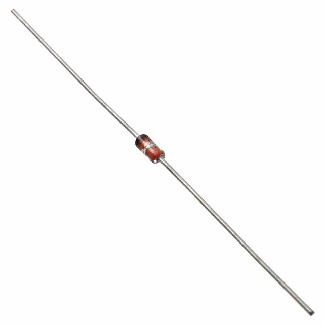


 工商网监
湘ICP备2023018690号
工商网监
湘ICP备2023018690号
