物料型号:1N5415至1N5420
器件简介:这些二极管是军用级别的快速恢复整流二极管,适用于高可靠性应用,工作峰值反向电压从50到600伏,采用无空洞玻璃封装和内部“Category 1”冶金键合。
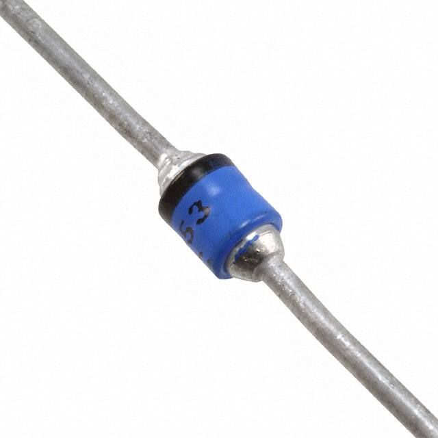
引脚分配:文档中没有明确提供引脚分配图,但提到了轴向引脚是锡/铅(Sn/Pb)覆盖铜,对于商业等级,提供符合RoHS标准的无铅焊锡。
参数特性:
- 工作峰值反向电压:1N5415为50V,1N5416为100V,1N5417为200V,1N5418为400V,1N5419为500V,1N5420为600V。
- 最大反向恢复时间:1N5415至1N5419为150ns至400ns,1N5420为250ns。
- 最大正向浪涌电流:未明确列出具体数值。
- 热阻:未提供具体数值。
功能详解:这些二极管具有快速恢复能力,适用于军事和其他高可靠性应用,包括整流桥、半桥、捕获二极管等。它们具有高正向浪涌电流能力、极低的热阻和控制的雪崩能力。
应用信息:适用于一般的整流器应用,包括整流桥、半桥、捕获二极管等。
封装信息:提供SQ-MELF(D-5B)表面贴装封装,重量为750毫克,符合EIA-296标准的胶带和卷轴选项。