1N5550US thru 1N5554US
Available on
commercial
versions
VOIDLESS HERMETICALLY SEALED SURFACE
MOUNT STANDARD RECOVERY GLASS RECTIFIERS
Qualified Levels:
JAN, JANTX, JANTXV
and JANS
Qualified to MIL-PRF-19500/420
DESCRIPTION
This “standard recovery” surface mount rectifier diode series is military qualified and is ideal
for high-reliability applications where a failure cannot be tolerated. These industry-recognized
5.0 amp rated rectifiers for working peak reverse voltages from 200 to 1000 volts are
hermetically sealed with voidless-glass construction using an internal “Category 1”
metallurgical bond. These devices are also available in axial-leaded packages for thru-hole
mounting. Microsemi also offers numerous other rectifier products to meet higher and lower
current ratings with various recovery time speeds.
Important: For the latest information, visit our website http://www.microsemi.com.
FEATURES
•
•
•
•
•
Surface mount equivalent of JEDEC registered 1N5550 thru 1N5554 series.
Voidless hermetically sealed glass package.
Extremely robust construction.
Quadruple-layer passivation.
Internal “Category 1” metallurgical bonds.
•
JAN, JANTX, JANTXV and JANS qualified versions available per MIL-PRF-19500/420.
•
RoHS compliant versions available (commercial grade only).
“B” SQ-MELF (D-5B)
Package
Also available in:
“B” Package
(axial-leaded)
1N5550 – 1N5554
APPLICATIONS / BENEFITS
•
•
•
•
•
•
•
•
Standard recovery 5 amp 200 to 1000 volts rectifiers series.
Military and other high-reliability applications.
General rectifier applications including bridges, half-bridges, catch diodes, etc.
High forward surge current capability.
Low thermal resistance.
Controlled avalanche with peak reverse power capability.
Extremely robust construction.
Inherently radiation hard as described in Microsemi “MicroNote 050”.
MAXIMUM RATINGS @ TA = 25 oC unless otherwise noted.
Parameters/Test Conditions
Junction and Storage Temperature
Thermal Resistance Junction-to-End Cap
(1)
Thermal Impedance @ 10 ms heating time
Maximum Forward Surge Current (8.3 ms half sine)
(2)
o
Average Rectified Forward Current
@ TEC = 130 C
(3)
o
Average Rectified Forward Current
@ TA = 55 C
o
@ TA = 100 C
Working Peak Reverse Voltage
1N5550US
1N5551US
1N5552US
1N5553US
1N5554US
Solder Temperature @ 10 s
Symbol
Value
TJ and TSTG
R ӨJEC
Z ӨJX
I FSM
I O(L)
(2)
I O2
(4)
I O3
V RWM
-65 to +175
6.5
1.5
100
5
3
2
200
400
600
800
1000
260
TSP
o
C
C/W
o
C/W
A
A
A
A
V
o
O
C
MSC – Lawrence
6 Lake Street,
Lawrence, MA 01841
Tel: 1-800-446-1158 or
(978) 620-2600
Fax: (978) 689-0803
MSC – Ireland
Gort Road Business Park,
Ennis, Co. Clare, Ireland
Tel: +353 (0) 65 6840044
Fax: +353 (0) 65 6822298
Website:
www.microsemi.com
See notes on next page.
T4-LDS-0230-1, Rev. 1 (111901)
Unit
©2011 Microsemi Corporation
Page 1 of 5
�1N5550US thru 1N5554US
MAXIMUM RATINGS
Notes: 1. Derate linearly at 66.6 mA/ºC above T EC = 100 ºC. An I O of up to 6 Amps is allowable provided that appropriate heat sinking or forced air
cooling maintains the junction temperature at or below +200 oC.
2. Derate linearly at 22.2 mA/ºC from +55 ºC to +100 oC.
3. These I O ratings are for a thermally (PC boards or other) mounting methods where the lead or end-cap temperatures cannot be maintained
and where thermal resistance from mounting point to ambient is still sufficiently controlled where T J(MAX) does not exceed 175 oC. This
equates to R θJX ≤ 47 ºC/W.
4. Derate linearly at 26.7 mA/°C above T A = +100 °C to +175 °C ambient.
MECHANICAL and PACKAGING
•
•
•
•
•
•
•
CASE: Hermetically sealed voidless hard glass with tungsten slugs.
TERMINALS: End caps are copper with tin/lead (Sn/Pb) finish. RoHS compliant matte-tin is available for commercial only.
MARKING: Cathode band only.
POLARITY: Cathode indicated by band.
TAPE & REEL option: Standard per EIA-481-B. Consult factory for quantities.
WEIGHT: 539 milligrams.
See Package Dimensions and recommended Pad Layout on last page.
PART NOMENCLATURE
JAN
1N5550
US
(e3)
Reliability Level
JAN = JAN Level
JANTX = JANTX Level
JANTXV = JANTXV Level
JANS = JANS Level
Blank = Commercial
RoHS Compliance
e3 = RoHS compliant (available
on commercial grade only)
Blank = non-RoHS compliant
MELF Package
JEDEC type number
See Electrical Characteristics
table
SYMBOLS & DEFINITIONS
Definition
Symbol
V BR
V RWM
IO
VF
IR
t rr
Minimum Breakdown Voltage: The minimum voltage the device will exhibit at a specified current.
Working Peak Reverse Voltage: The maximum peak voltage that can be applied over the operating temperature range
excluding all transient voltages (ref JESD282-B).
Average Rectified Output Current: The Output Current averaged over a full cycle with a 50 Hz or 60 Hz sine-wave
input and a 180 degree conduction angle.
Maximum Forward Voltage: The maximum forward voltage the device will exhibit at a specified current.
Maximum Reverse Current: The maximum reverse (leakage) current that will flow at the specified voltage and
temperature.
Reverse Recovery Time: The time interval between the instant the current passes through zero when changing from
the forward direction to the reverse direction and a specified decay point after a peak reverse current occurs.
T4-LDS-0230-1, Rev. 1 (111901)
©2011 Microsemi Corporation
Page 2 of 5
�1N5550US thru 1N5554US
ELECTRICAL CHARACTERISTICS @ TA = 25 oC unless otherwise noted.
TYPE
1N5550US
1N5551US
1N5552US
1N5553US
1N5554US
MINIMUM
BREAKDOWN
VOLTAGE
V BR
I R @ 50 µA
Volts
220
440
660
880
1100
FORWARD VOLTAGE
V F @ 9 A (pk)
MIN.
Volts
0.6 V (pk)
0.6 V (pk)
0.6 V (pk)
0.6 V (pk)
0.6 V (pk)
MAX.
Volts
1.2 V (pk)
1.2 V (pk)
1.2 V (pk)
1.3 V (pk)
1.3 V (pk)
MAXIMUM
REVERSE
CURRENT
I R @ V RWM
REVERSE
RECOVERY
t rr
(Note 1)
µA
µs
2.0
2.0
2.0
2.0
2.0
1.0
1.0
1.0
1.0
1.0
NOTE 1: I F = 0.5 A, I RM = 1.0 A, I R(REC) = .250 A.
T4-LDS-0230-1, Rev. 1 (111901)
©2011 Microsemi Corporation
Page 3 of 5
�1N5550US thru 1N5554US
o
ZӨJX ( C/Watt)
GRAPHS
t H Heating Time (seconds)
IF – Forward Current (A)
FIGURE 1
Maximum Thermal Impedance
V F – Forward Voltage (V)
FIGURE 4
Typical Forward Voltage vs. Forward Current
T4-LDS-0230-1, Rev. 1 (111901)
©2011 Microsemi Corporation
Page 4 of 5
�1N5550US thru 1N5554US
PACKAGE DIMENSIONS
Ltr
Inch
Millimeters
MIN
MAX
MIN
BL
.200
.275
5.08
MAX
6.99
BD
.137
.186
3.48
4.72
ECT
.019
.034
0.48
0.86
S
.003
---
0.08
---
NOTES:
1. Dimensions are in inches.
2. Millimeters are given for general information only.
3. Dimensions are pre-solder dip.
4. Minimum clearance of glass body to mounting surface on all orientations.
5. In accordance with ASME Y14.5M, diameters are equivalent to Φx symbology.
6. This package outline has also previously been identified as “D5B”.
PAD LAYOUT
Ltr
Inch
Millimeters
A
0.288
7.32
B
0.070
1.78
C
0.155
3.94
Note: If mounting requires
adhesive separate from the solder,
an additional 0.080 inch diameter
contact may be placed in the center
between the pads as an optional
spot for cement.
T4-LDS-0230-1, Rev. 1 (111901)
©2011 Microsemi Corporation
Page 5 of 5
�
很抱歉,暂时无法提供与“1N5553US/TR”相匹配的价格&库存,您可以联系我们找货
免费人工找货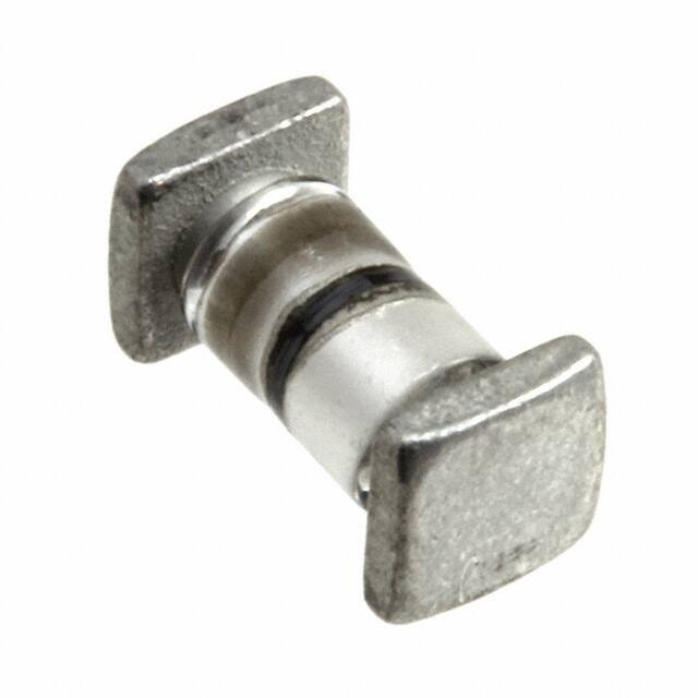


 工商网监
湘ICP备2023018690号
工商网监
湘ICP备2023018690号
