Obsolete Device
27C256
256K (32K x 8) CMOS EPROM
30
31
1
32
2
A7
A12
VPP
NU
Vcc
A14
A13
3
4
5
29
6
28
7
27
8
9
10
11
26
25
24
23
A8
A9
A11
NC
OE
A10
CE
O7
O6
20
19
18
17
21
16
22
13
15
12
14
A6
A5
A4
A3
A2
A1
A0
NC
O0
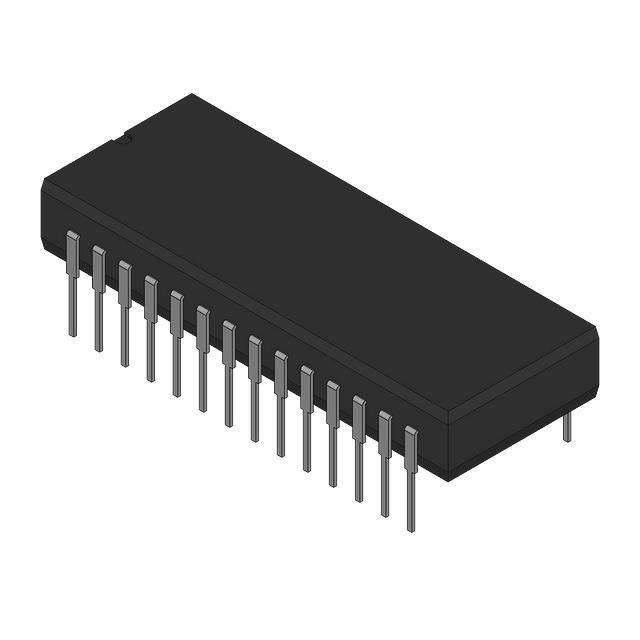
DIP/SOIC
VPP
A12
A7
A6
A5
A4
A3
A2
A1
A0
O0
O1
O2
VSS
1
2
3
4
5
6
7
8
9
10
11
12
13
14
27C256
DESCRIPTION
PLCC
27C256
• High speed performance
- 90 ns access time available
• CMOS Technology for low power consumption
- 20 mA Active current
- 100 µA Standby current
• Factory programming available
• Auto-insertion-compatible plastic packages
• Auto ID aids automated programming
• Separate chip enable and output enable controls
• High speed “express” programming algorithm
• Organized 32K x 8: JEDEC standard pinouts
- 28-pin Dual-in-line package
- 32-pin PLCC Package
- 28-pin SOIC package
- Tape and reel
• Data Retention > 200 years
• Available for the following temperature ranges:
- Commercial:
0°C to +70°C
- Industrial:
-40°C to +85°C
- Automotive:
-40°C to +125°C
PACKAGE TYPES
O1
O2
VSS
NU
O3
O4
O5
FEATURES
28
27
26
25
24
23
22
21
20
19
18
17
16
15
VCC
A14
A13
A8
A9
A11
OE
A10
CE
O7
O6
O5
O4
O3
The Microchip Technology Inc. 27C256 is a CMOS
256K bit electrically Programmable Read Only Memory
(EPROM). The device is organized as 32K words by 8
bits (32K bytes). Accessing individual bytes from an
address transition or from power-up (chip enable pin
going low) is accomplished in less than 90 ns. This very
high speed device allows the most sophisticated microprocessors to run at full speed without the need for
WAIT states. CMOS design and processing enables
this part to be used in systems where reduced power
consumption and reliability are requirements.
A complete family of packages is offered to provide the
most flexibility in applications. For surface mount applications, PLCC, or SOIC packaging is available. Tape
and reel packaging is also available for PLCC or SOIC
packages.
2004 Microchip Technology Inc.
DS11001N-page 1
�27C256
1.0
ELECTRICAL CHARACTERISTICS
1.1
Maximum Ratings*
TABLE 1-1:
PIN FUNCTION TABLE
Name
Function
VCC and input voltages w.r.t. VSS ........ -0.6V to +7.25V
A0-A14
VPP voltage w.r.t. VSS during
programming ....................................... -0.6V to +14.0V
CE
Chip Enable
OE
Output Enable
Output voltage w.r.t. VSS ................-0.6V to VCC +1.0V
VPP
Programming Voltage
Storage temperature ..........................-65°C to +150°C
O0 - O7
Ambient temp. with power applied .....-65°C to +125°C
VCC
+5V Power Supply
*Notice: Stresses above those listed under “Maximum Ratings”
may cause permanent damage to the device. This is a stress rating only and functional operation of the device at those or any
other conditions above those indicated in the operation listings of
this specification is not implied. Exposure to maximum rating conditions for extended periods may affect device reliability.
VSS
Ground
NC
No Connection; No Internal Connection
NU
Not Used; No External Connection Is
Allowed
Voltage on A9 w.r.t. VSS ...................... -0.6V to +13.5V
TABLE 1-2:
Address Inputs
Data Output
READ OPERATION DC CHARACTERISTICS
VCC = +5V (±10%)
Commercial:
Industrial:
Extended (Automotive):
Parameter
Tamb = 0°C to +70°C
Tamb = -40°C to +85°C
Tamb = -40°C to +125°C
Part*
Status
Symbol
Min.
Max.
Units
Conditions
Input Voltages
all
Logic "1"
Logic "0"
VIH
VIL
2.0
-0.5
VCC+1
0.8
V
V
Input Leakage
all
—
ILI
-10
10
µA
VIN = 0 to VCC
Output Voltages
all
Logic "1"
Logic "0"
VOH
VOL
2.4
0.45
V
V
IOH = -400 µA
IOL = 2.1 mA
Output Leakage
all
—
ILO
-10
10
µA
VOUT = 0V to VCC
Input Capacitance
all
—
CIN
—
6
pF
VIN = 0V; Tamb = 25°C;
f = 1 MHz
Output Capacitance
all
—
COUT
—
12
pF
VOUT = 0V; Tamb = 25°C;
f = 1 MHz
Power Supply Current,
Active
C
I,E
TTL input
TTL input
ICC1
ICC2
—
—
20
25
mA
mA
VCC = 5.5V; VPP = VCC
f = 1 MHz;
OE = CE = VIL;
IOUT = 0 mA;
VIL = -0.1 to 0.8V;
VIH = 2.0 to VCC;
Note 1
Power Supply Current,
Standby
C
I, E
all
TTL input
TTL input
CMOS input
ICC(S)
—
2
3
100
mA
mA
µA
all
all
Read Mode
Read Mode
IPP
VPP
100
VCC
µA
V
IPP Read Current
VPP Read Voltage
VCC-0.7
CE = VCC ± 0.2V
VPP = 5.5V
* Parts: C=Commercial Temperature Range; I, E=Industrial and Extended Temperature Ranges
Note 1: Typical active current increases .75 mA per MHz up to operating frequency for all temperature ranges.
DS11001N-page 2
2004 Microchip Technology Inc.
�27C256
TABLE 1-3:
READ OPERATION AC CHARACTERISTICS
AC Testing Waveform:
Output Load:
Input Rise and Fall Times:
Ambient Temperature:
VIH = 2.4V and VIL = 0.45V; VOH = 2.0V VOL = 0.8V
1 TTL Load + 100 pF
10 ns
Commercial:
Tamb = 0°C to +70°C
Industrial:
Tamb = -40°C to +85°C
Automotive:
Tamb = -40°C to +125°C
27C256-90* 27C256-10* 27C256-12 27C256-15 27C256-20
Parameter
Sym
Units Conditions
Min
Max
Min
Max
Min
Max
Min
Max Min
Max
Address to Output
Delay
tACC
—
90
—
100
—
120
—
150
—
200
ns
CE=OE =VIL
CE to Output Delay
tCE
—
90
—
100
—
120
—
150
—
200
ns
OE = VIL
OE to Output Delay
tOE
—
40
—
45
—
55
—
65
—
75
ns
CE = VIL
CE or OE to O/P
High Impedance
tOFF
0
30
0
30
0
35
0
50
0
55
ns
Output Hold from
Address CE or OE,
whichever goes first
tOH
0
—
0
—
0
—
0
—
0
—
ns
* -10, -90 AC Testing Waveform: VIH = 2.4V and VIL = .45V; VOH = 1.5V and VOL = 1.5V
Output Load: 1 TTL Load + 30pF
FIGURE 1-1:
READ WAVEFORMS
V IH
Address Valid
Address
V IL
V IH
CE
V IL
t CE(2)
V IH
OE
V IL
Outputs
O0 - O7
V OH
t OFF(1,3)
t OH
t OE(2)
High Z
High Z
Valid Output
V OL
t ACC
Notes: (1) t OFF is specified for OE or CE, whichever occurs first
(2) OE may be delayed up to t CE - t OE after the falling edge of CE without impact on t
(3) This parameter is sampled and is not 100% tested.
2004 Microchip Technology Inc.
CE
DS11001N-page 3
�27C256
TABLE 1-4:
PROGRAMMING DC CHARACTERISTICS
Ambient Temperature: Tamb = 25°C ± 5°C
VCC = 6.5V ± 0.25V, VPP = VH = 13.0V ± 0.25V
Parameter
Status
Symbol
Min
Max.
Units
Input Voltages
Logic”1”
Logic”0”
VIH
VIL
2.0
-0.1
VCC+1
0.8
V
V
Input Leakage
—
ILI
-10
10
µA
VIN = 0V to VCC
Logic”1”
Logic”0”
VOH
VOL
2.4
0.45
V
V
IOH = -400 µA
IOL = 2.1 mA
VCC Current, program & verify
—
ICC2
—
20
mA
Note 1
VPP Current, program
—
IPP2
—
25
mA
Note 1
A9 Product Identification
—
VH
11.5
12.5
V
Output Voltages
Conditions
Note 1: VCC must be applied simultaneously or before VPP and removed simultaneously or after VPP
TABLE 1-5:
PROGRAMMING AC CHARACTERISTICS
for Program, Program Verify
and Program Inhibit Modes
Parameter
AC Testing Waveform: VIH=2.4V and VIL=0.45V; VOH=2.0V; VOL=0.8V
Output Load:
1 TTL Load + 100pF
Ambient Temperature: Tamb=25°C ± 5°C
VCC= 6.5V ± 0.25V, VPP = VH = 13.0V ± 0.25V
Symbol
Min.
Max.
Units
Address Set-Up Time
tAS
2
—
µs
Data Set-Up Time
tDS
2
—
µs
Data Hold Time
tDH
2
—
µs
Address Hold Time
tAH
0
—
µs
Float Delay (2)
tDF
0
130
ns
VCC Set-Up Time
tVCS
2
—
µs
Program Pulse Width (1)
tPW
95
105
µs
CE Set-Up Time
tCES
2
—
µs
OE Set-Up Time
tOES
2
—
µs
VPP Set-Up Time
tVPS
2
—
µs
Data Valid from OE
tOE
—
100
ns
Remarks
100 µs typical
Note 1: For express algorithm, initial programming width tolerance is 100 µs ±5%.
2: This parameter is only sampled and not 100% tested. Output float is defined as the point where data is no
longer driven (see timing diagram).
DS11001N-page 4
2004 Microchip Technology Inc.
�27C256
FIGURE 1-2:
PROGRAMMING WAVEFORMS
Program
Verify
V IH
Address
Address Stable
V IL
t AS
t AH
V IH
High Z
Data
Data Stable
V IL
t DS
Data Out Valid
t DF
(1)
t DH
13.0V(2)
V PP
t VPS
5.0V
6.5V(2)
V CC
t VCS
5.0V
V IH
CE
V IL
t OES
t PW
V IH
OE
t OE
(1)
V IL
Notes:
TABLE 1-6:
(1) t DF and t OE are characteristics of the device but must be accommodated by the programmer
(2) V CC = 6.5 V ±0.25V, V PP = V H = 13.0V ±0.25V for express algorithm
MODES
Operation Mode
CE
OE
VPP
A9
O0 - O7
Read
VIL
VIL
VCC
X
DOUT
Program
VIL
VIH
VH
X
DIN
Program Verify
VIH
VIL
VH
X
DOUT
Program Inhibit
VIH
VIH
VH
X
High Z
Standby
VIH
X
VCC
X
High Z
Output Disable
VIL
VIH
VCC
X
High Z
Identity
VIL
VIL
VCC
VH
Identity Code
X = Don’t Care
1.2
Read Mode
(See Timing Diagrams and AC Characteristics)
Read Mode is accessed when:
a)
b)
For Read operations, if the addresses are stable, the
address access time (tACC) is equal to the delay from
CE to output (tCE). Data is transferred to the output
after a delay from the falling edge of OE (tOE).
the CE pin is low to power up (enable) the chip
the OE pin is low to gate the data to the output
pins
2004 Microchip Technology Inc.
DS11001N-page 5
�27C256
1.3
Standby Mode
The standby mode is defined when the CE pin is high
(VIH) and a program mode is not defined.
When these conditions are met, the supply current will
drop from 20 mA to 100 µA.
1.4
Output Enable
This feature eliminates bus contention in multiple bus
microprocessor systems and the outputs go to a high
impedance when the following condition is true:
• The OE pin is high and the program mode is not
defined.
1.5
Erase Mode (U.V. Windowed
Versions)
Windowed products offer the ability to erase the memory array. The memory matrix is erased to the all 1’s
state when exposed to ultraviolet light. To ensure complete erasure, a dose of 15 watt-second/cm2 is
required. This means that the device window must be
placed within one inch and directly underneath an ultraviolet lamp with a wavelength of 2537 Angstroms,
intensity of 12,000µW/cm2 for approximately 20 minutes.
1.6
Programming Mode
The Express Algorithm has been developed to improve
on the programming throughput times in a production
environment. Up to ten 100-microsecond pulses are
applied until the byte is verified. No overprogramming
is required. A flowchart of the express algorithm is
shown in Figure 1-3.
Programming takes place when:
a)
b)
c)
d)
VCC is brought to the proper voltage,
VPP is brought to the proper VH level,
the OE pin is high, and
the CE pin is low.
1.7
Verify
After the array has been programmed it must be verified to ensure all the bits have been correctly programmed. This mode is entered when all the following
conditions are met:
VCC is at the proper level,
VPP is at the proper VH level,
the CE line is high, and
the OE line is low.
a)
b)
c)
d)
1.8
Inhibit
When programming multiple devices in parallel with different data, only CE need be under separate control to
each device. By pulsing the CE line low on a particular
device, that device will be programmed; all other
devices with CE held high will not be programmed with
the data, although address and data will be available on
their input pins.
1.9
Identity Mode
In this mode specific data is output which identifies the
manufacturer as Microchip Technology Inc. and device
type. This mode is entered when Pin A9 is taken to VH
(11.5V to 12.5V). The CE and OE lines must be at VIL.
A0 is used to access any of the two non-erasable bytes
whose data appears on O0 through O7.
Pin
Identity
Manufacturer
Device Type*
Input
Output
H
e
x
A0
0 O O O O O O O
7 6 5 4 3 2 1 0
VIL
VIH
0 0 1 0 1 0 0 1 29
1 0 0 0 1 1 0 0 8C
* Code subject to change
Since the erased state is “1” in the array, programming
of “0” is required. The address to be programmed is set
via pins A0-A14 and the data to be programmed is presented to pins O0-O7. When data and address are stable, a low going pulse on the CE line programs that
location.
DS11001N-page 6
2004 Microchip Technology Inc.
�27C256
FIGURE 1-3:
PROGRAMMING EXPRESS ALGORITHM
Conditions:
Tamb = 25•C ±5•C
V CC = 6.5 ±0.25V
V PP = 13.0 ±0.25V
Start
ADDR = First Location
V CC = 6.5V
V PP = 13.0V
X=0
Program one 100 µs pulse
Increment X
Verify
Byte
Pass
Fail
No
Yes
X = 10 ?
Last
Address?
Device
Failed
Yes
No
Increment Address
V CC = V PP = 4.5V, 5.5V
Device
Passed
2004 Microchip Technology Inc.
Yes
All
bytes
= original
data?
No
Device
Failed
DS11001N-page 7
�27C256
27C256 Product Identification System
To order or to obtain information (e.g., on pricing or delivery), please use listed part numbers, and refer to factory or listed sales offices.
27C256
– 90 I
/TS
Package:
Temperature
Range:
Access
Time:
Device
DS11001N-page 8
L = Plastic Leaded Chip Carrier
P = Plastic DIP (Mil 600)
SO = Plastic SOIC (Mil 300)
Blank = 0°C to +70°C
I = -40°C to +85°C
E = -40°C to +125°C
90
10
12
15
20
27C256
=
=
=
=
=
90 ns
100 ns
120 ns
150 ns
200 ns
256K (32K x 8) CMOS EPROM
2004 Microchip Technology Inc.
�Note the following details of the code protection feature on Microchip devices:
•
Microchip products meet the specification contained in their particular Microchip Data Sheet.
•
Microchip believes that its family of products is one of the most secure families of its kind on the market today, when used in the
intended manner and under normal conditions.
•
There are dishonest and possibly illegal methods used to breach the code protection feature. All of these methods, to our
knowledge, require using the Microchip products in a manner outside the operating specifications contained in Microchip’s Data
Sheets. Most likely, the person doing so is engaged in theft of intellectual property.
•
Microchip is willing to work with the customer who is concerned about the integrity of their code.
•
Neither Microchip nor any other semiconductor manufacturer can guarantee the security of their code. Code protection does not
mean that we are guaranteeing the product as “unbreakable.”
Code protection is constantly evolving. We at Microchip are committed to continuously improving the code protection features of our
products. Attempts to break Microchip’s code protection feature may be a violation of the Digital Millennium Copyright Act. If such acts
allow unauthorized access to your software or other copyrighted work, you may have a right to sue for relief under that Act.
Information contained in this publication regarding device
applications and the like is intended through suggestion only
and may be superseded by updates. It is your responsibility to
ensure that your application meets with your specifications.
No representation or warranty is given and no liability is
assumed by Microchip Technology Incorporated with respect
to the accuracy or use of such information, or infringement of
patents or other intellectual property rights arising from such
use or otherwise. Use of Microchip’s products as critical
components in life support systems is not authorized except
with express written approval by Microchip. No licenses are
conveyed, implicitly or otherwise, under any intellectual
property rights.
Trademarks
The Microchip name and logo, the Microchip logo, Accuron,
dsPIC, KEELOQ, microID, MPLAB, PIC, PICmicro, PICSTART,
PRO MATE, PowerSmart, rfPIC, and SmartShunt are
registered trademarks of Microchip Technology Incorporated
in the U.S.A. and other countries.
AmpLab, FilterLab, MXDEV, MXLAB, PICMASTER, SEEVAL,
SmartSensor and The Embedded Control Solutions Company
are registered trademarks of Microchip Technology
Incorporated in the U.S.A.
Analog-for-the-Digital Age, Application Maestro, dsPICDEM,
dsPICDEM.net, dsPICworks, ECAN, ECONOMONITOR,
FanSense, FlexROM, fuzzyLAB, In-Circuit Serial
Programming, ICSP, ICEPIC, Migratable Memory, MPASM,
MPLIB, MPLINK, MPSIM, PICkit, PICDEM, PICDEM.net,
PICLAB, PICtail, PowerCal, PowerInfo, PowerMate,
PowerTool, rfLAB, rfPICDEM, Select Mode, Smart Serial,
SmartTel and Total Endurance are trademarks of Microchip
Technology Incorporated in the U.S.A. and other countries.
SQTP is a service mark of Microchip Technology Incorporated
in the U.S.A.
All other trademarks mentioned herein are property of their
respective companies.
© 2004, Microchip Technology Incorporated, Printed in the
U.S.A., All Rights Reserved.
Printed on recycled paper.
Microchip received ISO/TS-16949:2002 quality system certification for
its worldwide headquarters, design and wafer fabrication facilities in
Chandler and Tempe, Arizona and Mountain View, California in
October 2003. The Company’s quality system processes and
procedures are for its PICmicro® 8-bit MCUs, KEELOQ® code hopping
devices, Serial EEPROMs, microperipherals, nonvolatile memory and
analog products. In addition, Microchip’s quality system for the design
and manufacture of development systems is ISO 9001:2000 certified.
2004 Microchip Technology Inc.
DS11001N-page 9
�WORLDWIDE SALES AND SERVICE
AMERICAS
China - Beijing
Singapore
Corporate Office
Unit 706B
Wan Tai Bei Hai Bldg.
No. 6 Chaoyangmen Bei Str.
Beijing, 100027, China
Tel: 86-10-85282100
Fax: 86-10-85282104
200 Middle Road
#07-02 Prime Centre
Singapore, 188980
Tel: 65-6334-8870 Fax: 65-6334-8850
2355 West Chandler Blvd.
Chandler, AZ 85224-6199
Tel: 480-792-7200
Fax: 480-792-7277
Technical Support: 480-792-7627
Web Address: www.microchip.com
China - Chengdu
3780 Mansell Road, Suite 130
Alpharetta, GA 30022
Tel: 770-640-0034
Fax: 770-640-0307
Rm. 2401-2402, 24th Floor,
Ming Xing Financial Tower
No. 88 TIDU Street
Chengdu 610016, China
Tel: 86-28-86766200
Fax: 86-28-86766599
Boston
China - Fuzhou
2 Lan Drive, Suite 120
Westford, MA 01886
Tel: 978-692-3848
Fax: 978-692-3821
Unit 28F, World Trade Plaza
No. 71 Wusi Road
Fuzhou 350001, China
Tel: 86-591-7503506
Fax: 86-591-7503521
Atlanta
Chicago
333 Pierce Road, Suite 180
Itasca, IL 60143
Tel: 630-285-0071
Fax: 630-285-0075
Dallas
16200 Addison Road, Suite 255
Addison Plaza
Addison, TX 75001
Tel: 972-818-7423
Fax: 972-818-2924
Detroit
Tri-Atria Office Building
32255 Northwestern Highway, Suite 190
Farmington Hills, MI 48334
Tel: 248-538-2250
Fax: 248-538-2260
Kokomo
2767 S. Albright Road
Kokomo, IN 46902
Tel: 765-864-8360
Fax: 765-864-8387
Los Angeles
25950 Acero St., Suite 200
Mission Viejo, CA 92691
Tel: 949-462-9523
Fax: 949-462-9608
San Jose
1300 Terra Bella Avenue
Mountain View, CA 94043
Tel: 650-215-1444
Fax: 650-961-0286
Toronto
6285 Northam Drive, Suite 108
Mississauga, Ontario L4V 1X5, Canada
Tel: 905-673-0699
Fax: 905-673-6509
China - Hong Kong SAR
Unit 901-6, Tower 2, Metroplaza
223 Hing Fong Road
Kwai Fong, N.T., Hong Kong
Tel: 852-2401-1200
Fax: 852-2401-3431
Taiwan
Kaohsiung Branch
30F - 1 No. 8
Min Chuan 2nd Road
Kaohsiung 806, Taiwan
Tel: 886-7-536-4816
Fax: 886-7-536-4817
Taiwan
Taiwan Branch
11F-3, No. 207
Tung Hua North Road
Taipei, 105, Taiwan
Tel: 886-2-2717-7175 Fax: 886-2-2545-0139
Taiwan
Taiwan Branch
13F-3, No. 295, Sec. 2, Kung Fu Road
Hsinchu City 300, Taiwan
Tel: 886-3-572-9526
Fax: 886-3-572-6459
EUROPE
China - Shanghai
Austria
Room 701, Bldg. B
Far East International Plaza
No. 317 Xian Xia Road
Shanghai, 200051
Tel: 86-21-6275-5700
Fax: 86-21-6275-5060
Durisolstrasse 2
A-4600 Wels
Austria
Tel: 43-7242-2244-399
Fax: 43-7242-2244-393
China - Shenzhen
Regus Business Centre
Lautrup hoj 1-3
Ballerup DK-2750 Denmark
Tel: 45-4420-9895 Fax: 45-4420-9910
Rm. 1812, 18/F, Building A, United Plaza
No. 5022 Binhe Road, Futian District
Shenzhen 518033, China
Tel: 86-755-82901380
Fax: 86-755-8295-1393
China - Shunde
Room 401, Hongjian Building, No. 2
Fengxiangnan Road, Ronggui Town, Shunde
District, Foshan City, Guangdong 528303, China
Tel: 86-757-28395507 Fax: 86-757-28395571
China - Qingdao
Rm. B505A, Fullhope Plaza,
No. 12 Hong Kong Central Rd.
Qingdao 266071, China
Tel: 86-532-5027355 Fax: 86-532-5027205
India
Divyasree Chambers
1 Floor, Wing A (A3/A4)
No. 11, O’Shaugnessey Road
Bangalore, 560 025, India
Tel: 91-80-22290061 Fax: 91-80-22290062
Japan
ASIA/PACIFIC
Yusen Shin Yokohama Building 10F
3-17-2, Shin Yokohama, Kohoku-ku,
Yokohama, Kanagawa, 222-0033, Japan
Tel: 81-45-471- 6166 Fax: 81-45-471-6122
Australia
Korea
Microchip Technology Australia Pty Ltd
Unit 32 41 Rawson Street
Epping 2121, NSW
Sydney, Australia
Tel: 61-2-9868-6733
Fax: 61-2-9868-6755
168-1, Youngbo Bldg. 3 Floor
Samsung-Dong, Kangnam-Ku
Seoul, Korea 135-882
Tel: 82-2-554-7200 Fax: 82-2-558-5932 or
82-2-558-5934
Denmark
France
Parc d’Activite du Moulin de Massy
43 Rue du Saule Trapu
Batiment A - ler Etage
91300 Massy, France
Tel: 33-1-69-53-63-20
Fax: 33-1-69-30-90-79
Germany
Steinheilstrasse 10
D-85737 Ismaning, Germany
Tel: 49-89-627-144-0
Fax: 49-89-627-144-44
Italy
Via Salvatore Quasimodo, 12
20025 Legnano (MI)
Milan, Italy
Tel: 39-0331-742611
Fax: 39-0331-466781
Netherlands
Waegenburghtplein 4
NL-5152 JR, Drunen, Netherlands
Tel: 31-416-690399
Fax: 31-416-690340
United Kingdom
505 Eskdale Road
Winnersh Triangle
Wokingham
Berkshire, England RG41 5TU
Tel: 44-118-921-5869
Fax: 44-118-921-5820
07/12/04
2004 Microchip Technology Inc.
�