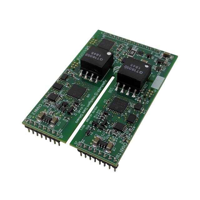
2ASC-12A1HP 1200V Dual-Channel Core Series
PRELIMINARY
2ASC-12A1HP – 1200V Dual-Channel
Augmented High Performance SiC Core 1
Optimized for Silicon Carbide (SiC) MOSFET Modules
Overview
The AgileSwitch 2ASC-12A1HP – 1200V Dual-Channel Augmented High Performance SiC Core 1 enables better
control and protection of most SiC MOSFET-based power systems. The 2ASC-12A1HP provides up to 10A of
peak current at an operating frequency of 100kHz. The high CMTI gate drive core includes an isolated DC/DC
converter and low capacitance isolation barrier for PWM signals and fault feedback. The Intelligent Configuration
Tool (ICT) will allow users to appropriately configure the Gate Driver Parameters to their application without
having to worry about changing hardware.
Software Programmable Features
Key Driver Features
•
•
•
•
•
•
•
•
•
•
•
•
•
•
•
•
•
TM
Augmented Turn-Off (ATOff) (Patented)
± VGS Gate Voltages
o Vgs Pos from +15V to +21V
o Vgs Neg from -5V to 0V
Power supply under-voltage lockout (UVLO)
Power supply over-voltage lockout (OVLO)
Desaturation detection settings
Dead time
Fault lockout settings
Automatic Reset settings
UL Compliant - 1200V SiC MOSFET Modules
Dual-Channel
Robust High-Noise-Immunity Design
Isolated Temperature Monitoring, PWM
Isolated High Voltage Monitoring, PWM
Compact 40x61mm form factor
2 X 3W output power
RoHS compliant
Up to 7 Unique Fault Conditions
Applications
•
•
•
•
•
•
Heavy Duty Vehicles
Induction Heating
Auxiliary Power Units
Battery Storage
Inverters
Wireless Charging
2ASC-12A1HP Spec Sheet V1.2
© 2019 AgileSwitch, LLC
Page 1 of 19
�2ASC-12A1HP 1200V Dual-Channel Core Series
PRELIMINARY
Contents
System Overview .................................................................................................................................................. 4
Absolute Maximum Ratings ................................................................................................................................. 4
Electrical Characteristics ....................................................................................................................................... 5
Interconnects ......................................................................................................................................................... 6
Module Adapter to Driver Core Connectors ..................................................................................................... 6
Core Programming Adapter .............................................................................................................................. 6
Core Assembly on Adapter Board ..................................................................................................................... 6
Method 1 - Soldering .................................................................................................................................... 6
Method 2 – Socket ........................................................................................................................................ 6
Pinout – Controller/Power to Driver Connection .............................................................................................. 7
14 PIN – J1 - Input ........................................................................................................................................ 7
8 PIN – J2 – Channel 2 (CH2) ...................................................................................................................... 7
8 PIN – J3 – Channel 1 (CH1) ...................................................................................................................... 7
Recommended Interface Circuitry ........................................................................................................................ 8
Primary ............................................................................................................................................................. 8
Block Diagram .............................................................................................................................................. 8
Buffer Schematic for Inputs on the Module Adapter Board .......................................................................... 8
Secondary ......................................................................................................................................................... 9
Drive Circuit ............................................................................................................................................... 10
Short Circuit Protection - DSAT Circuit ..................................................................................................... 11
DC Link monitor ......................................................................................................................................... 12
Timing Diagrams ................................................................................................................................................ 13
Timing Diagram Values .................................................................................................................................. 14
Temperature and High Voltage PWM Monitoring .......................................................................................... 15
Temperature Monitor .................................................................................................................................. 15
DC Link Voltage Monitor ........................................................................................................................... 16
Generic Sample Factory Settings ........................................................................................................................ 16
Performance & Interconnect Settings .............................................................................................................. 16
Fault and Monitoring Conditions .................................................................................................................... 16
Important Precautions ......................................................................................................................................... 17
Software Configurable Parameters ...................................................................................................................... 17
Reference Designs .............................................................................................................................................. 17
2ASC-12A1HP Spec Sheet V1.2
© 2019 AgileSwitch, LLC
Page 2 of 19
�2ASC-12A1HP 1200V Dual-Channel Core Series
PRELIMINARY
Mechanical Dimensions ...................................................................................................................................... 18
Revisions ............................................................................................................................................................ 18
Legal Disclaimer ................................................................................................................................................. 19
Patent Notices ..................................................................................................................................................... 19
Manufacturer ....................................................................................................................................................... 19
2ASC-12A1HP Spec Sheet V1.2
© 2019 AgileSwitch, LLC
Page 3 of 19
�2ASC-12A1HP 1200V Dual-Channel Core Series
PRELIMINARY
System Overview
The basic topology of the driver core is shown in Figure 1.
Figure 1: 2ASC-12A1HP Block Diagram
Absolute Maximum Ratings
Interaction of maximum ratings is dependent on operating conditions
Parameter
Supply Voltage
Peak Gate Current
Input Logic Levels
Output Power per Gate
Switching Frequency
Isolation Voltage
Working Voltage
Creepage Distance
𝑑𝑉/𝑑𝑡
Operating Temperature
Storage Temperature
2ASC-12A1HP Spec Sheet V1.2
Description
VCC to GND
Note 1
To GND
Min
0
-10
-0.5
Note 2
Primary to Secondary VAC RMS 1 min
Primary to Secondary, Secondary to Secondary
Primary to Secondary Side
Rate of change input to output
Ambient Operating Temperature
© 2019 AgileSwitch, LLC
8
100
-40
-40
Max
16.5
10
5
3
100
3750
1200
+85
+90
Unit
V
A
V
W
kHz
V
V
mm
kV/μs
°C
°C
Page 4 of 19
�2ASC-12A1HP 1200V Dual-Channel Core Series
PRELIMINARY
Electrical Characteristics
Conditions: VSUP = +15.0 V, VIN_LOGIC = 5V, MOSFET (Ciss = 11.7nF; Qg = 1025nC)
Power Supply
Description
Min
Supply Voltage
VCC to GND
14
Supply Current
Without Load
Supply Current
With Load, Note 3
UVLO Level-HI and LO*
Primary Side low voltage detect fault level
13.2
Secondary Side low voltage detect fault level,
UVLO Level-HI and LO*
13.5
Note 3
OVLO Level-HI and LO*
Primary Side high voltage detect fault level
Secondary Side high voltage fault detect level,
OVLO Level-HI & LO*
Note 3
Signal I/O
Input Impedance
VIN Low
VIN High
Gate Output Voltage Low*
Gate Output Voltage High*
Fault Output Voltage
Fault Output Current
Switching Frequency
DC Link & Temp Monitoring
DC Link & Temp Monitoring
DC Link & Temp Monitoring
DC Link Voltage Trip*
Temperature Trip*
MOSFET Short Protection
Desat Monitor Voltage*
TDSAT*
Response Time after Fault
Description
5V - Hi and Lo side input
5V - Turn-off threshold
5V – Turn-on Threshold
Note 5
Note 5
Fault lines are open collect with 5mA load
Note 4
Note 2
High Voltage (HV) & Temp Monitoring
Output
PWM Frequency
Output Impedance, User defined on Adapter
Board
Note 5
Note 5
Min
1
Description
Between Drain and Sink of MOSFET, Note 3,
Note 5
Activation after MOSFET Turn on, Note 5
Min
3
0.5
Typ
15
110
250
13.5
20.5
Max
16
Unit
V
mA
mA
V
V
16
24.65
16.5
V
V
Typ
Max
-4
+21
24
10
TBD
Unit
MΩ
V
V
V
V
V
mA
kHz
5
V
1.25
3.5
-6
+17
0.3
0
31.5
50 1%
0
25
kHz
Ω
1100
165
V
°C
Typ
4.5
Max
10
Unit
V
1.5
1.75
200
μs
ns
Note 1: Input signal should not be activated until 20 ms after power is applied to allow on board DC-DC converter to stabilize.
Note 2: Actual maximum switching speed is a function of gate capacitance.
Note 3: SiC MOSFET dependant, conditions listed above assume a MOSFET with Ciss = 11.7nF & Qg = 1025nC operating at 50kHz
Note 4: Fault lines are open collector and require a pull-up resistor, 2KΩ recommended
Note 5: Software Configurable
*Note: For Software configurable parameters, the available range of values are listed in the table
2ASC-12A1HP Spec Sheet V1.2
© 2019 AgileSwitch, LLC
Page 5 of 19
�2ASC-12A1HP 1200V Dual-Channel Core Series
PRELIMINARY
Interconnects
Module Adapter to Driver Core Connectors
Ref
J1
J2, J3
Connector
Input
Ch 1, Ch 2
Type
14 Pin, 2mm pitch spacing
8 Pin, 2mm pitch spacing
Manufacturer Part Number
NRPN141PAEN-RC
NRPN081PAEN-RC
Core Programming Adapter
Ref
J4
Connector
Programming
Type
6 Pin, 1.27mm pitch
spacing
Manufacturer Part Number
TC2030-IDC-NL
Figure 2: Interconnect Locations on PCB
Core Assembly on Adapter Board
Method 1 - Soldering
2ASC-12A1HP can be directly soldered onto an Adapter Board without the need for additional support.
Method 2 – Socket
2ASC-12A1HP can be plugged into female sockets on an Adapter Board.
Recommended Sockets
Ref
J1
J2, J3
Connector
Input
Ch 1, Ch 2
2ASC-12A1HP Spec Sheet V1.2
Type
14 Pin, 2mm pitch spacing
8 Pin, 2mm pitch spacing
Manufacturer Part Number
NPPN141BFCN-RC
NPPN081BFCN-RC
© 2019 AgileSwitch, LLC
Page 6 of 19
�2ASC-12A1HP 1200V Dual-Channel Core Series
PRELIMINARY
Pinout – Controller/Power to Driver Connection
14 PIN – J1 - Input
Pin
No
1
2
3
4
5
6
7
8
9
10
11
12
13
14
Signal
Function
VCC
VCC
+5V Out
AL-F
CH2-F
CH2-Trig
CH1-F
CH1-Trig
TE-P
HV-F
TE-F
F-RS
GND
GND
+15V Supply Voltage
+15V Supply Voltage
+5V Output to drive primary side electronics
All Faults (Active when CH1-F or CH2-F)
Channel 2 Fault Output
Channel 2 Trigger Input
Channel 1 Fault Output
Channel 1 Trigger Input
Non-Isolated Temperature Monitoring
Isolated DC Link Voltage Monitoring
Isolated Temperature Monitoring
Fault Reset (Auto Reset Optional)
Ground
Ground
8 PIN – J2 – Channel 2 (CH2)
Pin
No
15
16
Signal
Function
21
CH2_DC
CH2_Temp
CH2 – (-)V_Sec
CH2_Sink
CH2_Source
CH2_GND
CH2 – (+)V_Sec
DC Link Monitor
Temperature Monitor
Negative Secondary Voltage
Sink
Source
Ground
Positive Secondary Voltage
22
CH2 DSAT
Vds Monitor
17
18
19
20
8 PIN – J3 – Channel 1 (CH1)
Pin
No
23
24
Signal
Function
CH1 DSAT
CH1 – (-)V_Sec
CH1_GND
Vds Monitor
Negative Unregulated Voltage
Ground
29
CH1_Sink
CH1_Source
CH1 – (+)V_Sec
CH1_DC
Sink
Source
Positive Unregulated Voltage
DC Link Monitor
30
CH1_Temp
Temperature Monitor
25
26
27
28
2ASC-12A1HP Spec Sheet V1.2
© 2019 AgileSwitch, LLC
Page 7 of 19
�2ASC-12A1HP 1200V Dual-Channel Core Series
PRELIMINARY
Recommended Interface Circuitry
Primary
Block Diagram
Figure 2 Input 14-Pin pinout diagram for 2ASC-12A1HP SiC Driver Core
Buffer Schematic for Inputs on the Module Adapter Board
The 2ASC-12A1HP has a standard 5V input logic. Based on the operating conditions, a 15V single ended input
or differential input may be required.
Figure 3 Input buffers on Module adapter board for differential & 15V Single Ended Inputs
2ASC-12A1HP Spec Sheet V1.2
© 2019 AgileSwitch, LLC
Page 8 of 19
�2ASC-12A1HP 1200V Dual-Channel Core Series
PRELIMINARY
Secondary
Figure 4 Output pinout diagram for 2ASC-12A1HP SiC Driver Core
Channels 1 & 2 can be used interchangeably as the HI or LO side.
On the HI Side the Temperature line should be floating and the DC Link monitor line should be grounded.
2ASC-12A1HP Spec Sheet V1.2
© 2019 AgileSwitch, LLC
Page 9 of 19
�2ASC-12A1HP 1200V Dual-Channel Core Series
PRELIMINARY
Drive Circuit
Gate Voltage (Vgs) limiting Zener diodes are recommend limiting the exposure of the SiC MOSFET Gate to high
voltage transients. The Zener diodes should be chosen based on the Vgs ratings of the SiC MOSFET.
The 2ASC-12A1HP has separate Source & Sink outputs to separate the charging and discharging paths.
The below equation can be used to estimate the drive current required for a given SiC MOSFET module:
𝐼𝑔 𝑝𝑒𝑎𝑘 =
𝑉𝑔𝑠+ + 𝑉𝑔𝑠−
𝑅𝑔 + 𝑅𝐺
𝐼𝑔 𝑝𝑒𝑎𝑘 – Peak Gate Current
𝑉𝑔𝑠+ – Positive Gate Voltage recommended by the SiC MOSFET Manufacturer
𝑉𝑔𝑠− – Negative Gate Voltage recommended by the SiC MOSFET Manufacturer
𝑅𝑔 – SiC MOSFET Module Internal Gate Resistance
𝑅𝐺 – External Gate Resistance on the Module Adapter Board
Note: 𝐼𝑔 𝑝𝑒𝑎𝑘 is a strong function of the module gate charge
In the implementation shown below in Figure 6, a totem pole driver provides the 2ASC-12A1HP with ~20A peak
current.
Figure 5 Recommended Hi-Side Drive Circuit for 2ASC-12A1HP SiC Driver Core
2ASC-12A1HP Spec Sheet V1.2
© 2019 AgileSwitch, LLC
Page 10 of 19
�2ASC-12A1HP 1200V Dual-Channel Core Series
PRELIMINARY
Short Circuit Protection - DSAT Circuit
SiC devices are limited in their Short Circuit withstand capability of 2-3us. It is therefore important to adopt the
appropriate short circuit protection parameters for the Gate Driver.
DSAT Blanking time and DSAT threshold voltage are two such important parameters and are software
configurable features on the 2ASC-12A1HP.
DSAT protection with sense diodes is the recommended method, shown below in Figure 7.
The DSAT lines are pulled up to +V_Sec via a 10kΩ pull up resistor on the 2ASC-12A1HP.
Figure 6 Recommended DSAT Sense Circuit for 2ASC-12A1HP SiC Driver Core
2ASC-12A1HP Spec Sheet V1.2
© 2019 AgileSwitch, LLC
Page 11 of 19
�2ASC-12A1HP 1200V Dual-Channel Core Series
PRELIMINARY
DC Link monitor
The 2ASC-12A1HP also features isolated DC Link Voltage monitoring and protection.
The 2ASC-12A1HP DC Link Monitor circuit performs two functions:
• Compares this monitored value against the DC Link Fault Threshold
• Converts the DC Link Voltage into a PWM
The resistor divider circuit shown in Figure 8 is recommended.
Figure 7 Recommended DC Link Monitor Circuit for 2ASC-12A1HP Core
2ASC-12A1HP Spec Sheet V1.2
© 2019 AgileSwitch, LLC
Page 12 of 19
�2ASC-12A1HP 1200V Dual-Channel Core Series
PRELIMINARY
Timing Diagrams
Figure 8 Signal input and output timing diagram.
Figure 9 Signal desaturation and fault diagram.
2ASC-12A1HP Spec Sheet V1.2
© 2019 AgileSwitch, LLC
Page 13 of 19
�2ASC-12A1HP 1200V Dual-Channel Core Series
PRELIMINARY
Timing Diagram Values
Conditions: VSUP = +15.0 V, Temp = 0 ºC to 85 ºC
Description
Symbol
Min
Minimum Pulse
TS1
TMIN
Width
Typ
Max
Unit
ns
250
Notes
The minimum pulse width is a factor
of the 2-Level Turn-Off Time
Delay Time
De-Glitch Time
Rise Time
TD
TR
200
80
ns
ns
ns
Fall Time
TF
90
ns
2-Level Turn-Off
Time
2-Level Turn-Off
Voltage
TS1
360
ns
Input signal de-glitch time
Measured from 10% to 90% points on
edge Measurement Point 1 – Fig. 10
Measured from 10% to 90% points on
edge Measurement Point 2 – Fig. 10
Software configurable
Vsoft
1.5
V
Software configurable
Desaturation Time
1st DSAT V
TDSAT
Vsoft D1
ns
V
Software configurable
Multi-Level Turn-Off – First DSAT
Step
First DSAT Time*
2nd DSAT V
TSD1
Vsoft D2
400
5
ns
V
Second DSAT Time*
Fault Time Delay
Fault Reset
Fault Response Time
Dead Time - Input
TSD2
TFLT
Fault_Res
TRESP
TNOV
200
5000
1000
200
1000
ns
ns
ns
ns
ns
First DSAT 2-level turn-off time
Multi-Level Turn-Off – Second DSAT
Step
Second DSAT 2-level turn-off time
Dead Time – Driver
Tcod
1000
ns
Reset Timing
Automatic Reset
(Optional)
Treset
1000
ns
ms
1400
1500
9
1600
5
Recommended Minimum Time
between Inputs
Minimum Time between drive signals
allowed by driver, software
configurable
Minimum Reset Time
Standard setting of 5 ms
*Note 3
Figure 10 Measurement points for rise and fall time
2ASC-12A1HP Spec Sheet V1.2
© 2019 AgileSwitch, LLC
Page 14 of 19
�2ASC-12A1HP 1200V Dual-Channel Core Series
PRELIMINARY
Temperature and High Voltage PWM Monitoring
The AgileSwitch 2ASC-12A1HP Driver provides two 31.5 kHz, 5.0V PWM output signals that monitor the
thermistor temperature (isolated or non-isolated) and the DC Link Voltage (High Side drain to Low Side source)
of the SiC MOSFET power module. The PWM signals have an output impedance of 510Ω. When combined
with an external low pass filter, these signals represent a real time, isolated voltage for both High Voltage and
Thermistor Temperature. A Sallen-Key active low pass filter can be used with these outputs as shown below
with a 2 kHz cut-off frequency. The cut-off frequency can be optimized for your application. For simplicity, a
simple RC low pass filter with 100 Hz cut-off frequency can also be used.
Figure 11 Example of a 2kHz Low Pass Filter
Temperature Monitor
The following table describes the correlation between the Thermistor Temperature and filtered Temperature
Monitor Output. This is based on an NTC thermistor that measures 5kΩ @ 25°C. In the event that a thermistor
is not part of the SiC Module the Recommended external Thermistor P/N is: TBD.
Output Voltage [V]
0.8
1.6
2.2
2.8
3.1
3.3
3.4
3.7
4.0
4.1
4.3
4.4
2ASC-12A1HP Spec Sheet V1.2
Temperature [°C]
-3
25
41
57
67
74
80
94
108
122
138
154
© 2019 AgileSwitch, LLC
Page 15 of 19
�2ASC-12A1HP 1200V Dual-Channel Core Series
PRELIMINARY
DC Link Voltage Monitor
The DC Link (HI Side drain to LO Side source) Monitor Output Voltage is 1% accurate from 50V to 1650V.
The PWM output is the ratio of the DC Link Voltage / 1700V. For example, an 825V DC Link Voltage, the
PWM output will be 50%. The linear equation for the Voltage Monitor PWM Output with a 2 kHz 4 pole filter
is:
𝑉𝐷𝐶 [𝑉] = 340 𝑋 𝑉𝑚𝑜𝑛𝑖𝑡𝑜𝑟
Generic Sample Factory Settings
AgileSwitch drivers are designed to provide safe, secure and efficient operation of the SiC MOSFET power
module, as well as to provide unparalleled information on the condition of the overall system.
Generic samples are set at the factory to perform certain actions (e.g. turn off the HI side or LO side of the SiC
MOSFET) and to report that a fault occurred based on performance parameters that occur outside of default ranges.
The tables below show the generic configuration.
Performance & Interconnect Settings
Parameter
Fault Reset
DC Link Voltage Fault
Temperature Fault
UVLO Primary
UVLO Secondary
OVLO Primary
OVLO Secondary
Generic Factory Setting
Auto
Enabled
Enabled
Enabled
Enabled
Enabled
Enabled
Value
5
900
125
13.2
20.2
16.5
24.65
Unit
ms
V
°C
V
V
V
V
Fault and Monitoring Conditions
Fault
Condition/Action
Generic
Sample
Default
Trigger
Values
Action on
IGBT if
Active
(Default
Setting)
Faults Low Active
HI Fault LO
Fault
All
Faults
Faults High Active
HI Fault LO
Fault
All
Fault
NO FAULTS
N/A
N/A
HIGH
HIGH
HIGH
LOW
LOW
LOW
DSAT/UVLO – HI
See Electrical
Characteristics
See Electrical
Characteristics
See Electrical
Characteristics
125 °C
Thermistor
Monitor
DC Link Voltage
above or below
setting
Failure to
Configure Gate
drivers
Turn Off HI &
LO Side
Turn Off HI
&LO Side
Turn Off HI &
LO Side
No Action
LOW
HIGH
LOW
HIGH
LOW
HIGH
HIGH
LOW
LOW
LOW
HIGH
HIGH
HIGH
HIGH
LOW
LOW
LOW
HIGH
HIGH
HIGH
LOW
LOW
LOW
HIGH
Turn Off HI &
LO Side
HIGH
HIGH
LOW
LOW
LOW
HIGH
Turn Off HI &
LO Side
LOW
LOW
LOW
HIGH
HIGH
HIGH
DSAT/UVLO – LO
OVLO
Temperature Fault
DC Link Voltage Fault
Power On
Configuration Fault*
*After power up, if all Fault lines are Active, then either there is a real fault (UVLO/DSAT) on both the HI and LO sides or there has been a software configuration failure.
2ASC-12A1HP Spec Sheet V1.2
© 2019 AgileSwitch, LLC
Page 16 of 19
�2ASC-12A1HP 1200V Dual-Channel Core Series
PRELIMINARY
Important Precautions
Caution: Handling devices with high voltages involves risk to life. It is imperative to
comply with all respective precautions and safety regulations.
When installing the core and adapter board, please make sure that power is turned off. Hot swapping may
cause damage to the IC components on the board.
AgileSwitch assumes that the core and adapter board have been mounted on the SiC MOSFET prior to
start-up testing. It is recommended that the user checks that the SiC MOSFET power modules are
operating inside the Specified Operating Area (SOA) as specified by the module manufacturer including
short circuit testing under very low load conditions.
Software Configurable Parameters
The software configurable parameters on the 2ASC-12A1HP can be modified using a GUI developed by
AgileSwitch. The code generated by this GUI is then downloaded to the driver. For further information regarding
the parameters and instructions on programming the driver, please refer to the below documents.
2ASC-12A1HP Software User Manual* (Coming Soon)
AgileSwitch Programming Instructions* (Coming Soon)
Reference Designs
AgileSwitch has developed Reference Module Adapter Boards for the 2ASC-12A1HP. These design data of these
adapter boards can be found here:
Module Package
Model Number
Module Manufacturers
62mm
62CA1
62mm
High
Performance
E, G Type Package
Automotive
62CA2
Wolfspeed, Semikron,
Infineon, Global Power
Wolfspeed
TBD
ASEP
2ASC-12A1HP Spec Sheet V1.2
Rohm
Infineon, Rohm,
Wolfspeed, StarPower
© 2019 AgileSwitch, LLC
Reference Module Adapter Board
Status
Contact Us for Design
Contact Us for Design
Contact Us for Design
Contact Us for Design
Page 17 of 19
�2ASC-12A1HP 1200V Dual-Channel Core Series
PRELIMINARY
Mechanical Dimensions
Figure 11: Dimensions of the 2ASC-12A1HP Core(+/- 0.1mm)
Dimensions are in mm.
Download the full drawing and model for additional details. * (Coming Soon)
Revisions
Prepared By
N. Satheesh
A. Fender
N. Satheesh
A. Fender
Approved By
Version
01
Date
8/31/2018
Description
Preliminary Release
1.1
10/4/2018
A. Fender
N. Satheesh
1.2
2
10/12/2018
3/22/2019
N. Satheesh
3
4/30/2019
Changed Secondary Pin-Out,
Added Interface Circuits, Updated Mechanical
Drawings
Updated Mechanical Drawing
Changed HI Side Termination; Clarified Software
Configurable Features;
Added to Adapter Board Compatibility Table
2ASC-12A1HP Spec Sheet V1.2
© 2019 AgileSwitch, LLC
Page 18 of 19
�2ASC-12A1HP 1200V Dual-Channel Core Series
PRELIMINARY
Legal Disclaimer
Information in this document is provided solely in connection with AGILESWITCH products. AGILESWITCH, LLC and its subsidiaries
(“AGILESWITCH”) reserve the right to make changes, corrections, modifications or improvements, to this document, and the products
and services described herein at any time, without notice.
All AGILESWITCH products are sold pursuant to AGILESWITCH’s terms and conditions of sale.
Purchasers are solely responsible for the choice, selection and use of AGILESWITCH products and services described herein, and
AGILESWITCH assumes no liability whatsoever relating to the choice, selection or use of the AGILESWITCH products and services
described herein.
No license, express or implied, by estoppel or otherwise, to any intellectual property rights is granted under this document. If any part of
this document refers to any third party products or services it shall not be deemed a license grant by AGILESWITCH for the use of such
third party products or services, or any intellectual property contained therein or considered as a warranty covering the use in any manner
whatsoever of such third party products or services or any intellectual property contained therein.
UNLESS OTHERWISE SET FORTH IN AGILESWITCH’S TERMS AND CONDITIONS OF SALE AGILESWITCH DISCLAIMS
ANY EXPRESS OR IMPLIED WARRANTY WITH RESPECT TO THE USE AND/OR SALE OF AGILESWITCH PRODUCTS
INCLUDING WITHOUT LIMITATION IMPLIED WARRANTIES OF MERCHANTABILITY, FITNESS FOR A PARTICULAR
PURPOSE (AND THEIR EQUIVALENTS UNDER THE LAWS OF ANY JURISDICTION), OR INFRINGEMENT OF ANY
PATENT, COPYRIGHT OR OTHER INTELLECTUAL PROPERTY RIGHT.
UNLESS EXPRESSLY APPROVED IN WRITING BY AN AUTHORIZED AGILESWITCH REPRESENTATIVE, AGILESWITCH
PRODUCTS ARE NOT RECOMMENDED, AUTHORIZED OR WARRANTED FOR USE IN MILITARY, AIR CRAFT, SPACE,
LIFE SAVING, OR LIFE SUSTAINING APPLICATIONS, NOR IN PRODUCTS OR SYSTEMS WHERE FAILURE OR
MALFUNCTION MAY RESULT IN PERSONAL INJURY, DEATH, OR SEVERE PROPERTY OR ENVIRONMENTAL DAMAGE.
AGILESWITCH PRODUCTS WHICH ARE NOT SPECIFIED AS "AUTOMOTIVE GRADE" MAY ONLY BE USED IN
AUTOMOTIVE APPLICATIONS AT USER’S OWN RISK.
Resale of AGILESWITCH products with provisions different from the statements and/or technical features set forth in this document
shall immediately void any warranty granted by AGILESWITCH for the AGILESWITCH product or service described herein and shall
not create or extend in any manner whatsoever, any liability of AGILESWITCH.
AGILESWITCH, the AGILESWITCH logo, AgileStack, AgileStack Communications and Stack Black Box are trademarks or registered
trademarks of AGILESWITCH, LLC in various countries. Any other names are the property of their respective owners.
EconoDual and PrimePACK are trademarks of Infineon Technologies AG.
Information in this document supersedes and replaces all information previously supplied.
Specifications are subject to change without notice.
© 2010-2019 AGILESWITCH LLC - All rights reserved www.AgileSwitch.com.
Patent Notices
Offering
AgileStackTM Power Stack
Gate Drivers for WBG Power
Semiconductors
Additional Patents Pending
Issued U.S. Patent Numbers
8,984,197
9,490,798
Manufacturer
AgileSwitch, LLC
2002 Ludlow Street #4
Philadelphia, PA 19103
United States
2ASC-12A1HP Spec Sheet V1.2
Tel:
Email:
Web:
+1-484-483-3256 (US)
+44 (0)1273 252994 (Europe)
info@AgileSwitch.com
www.AgileSwitch.com
© 2019 AgileSwitch, LLC
Page 19 of 19
�


 工商网监
湘ICP备2023018690号
工商网监
湘ICP备2023018690号

