TECHNICAL DATA SHEET
6 Lake Street, Lawrence, MA 01841
1-800-446-1158 / (978) 620-2600 / Fax: (978) 689-0803
Website: http: //www.microsemi.com
Gort Road Business Park, Ennis, Co. Clare, Ireland
Tel: +353 (0) 65 6840044 Fax: +353 (0) 65 6822298
PNP SILICON SWITCHING TRANSISTOR
Qualified per MIL-PRF-19500/357
DEVICES
LEVELS
2N3634
2N3634L
2N3634UB
2N3635
2N3635L
2N3635UB
2N3636
2N3636L
2N3636UB
2N3637
2N3637L
2N3637UB
JAN
JANTX
JANTXV
JANS
ABSOLUTE MAXIMUM RATINGS (TC = +25°C unless otherwise noted)
Symbol
2N3634*
2N3635*
2N3636*
2N3637*
Unit
Collector-Emitter Voltage
VCEO
140
175
Vdc
Collector-Base Voltage
VCBO
140
175
Vdc
Emitter-Base Voltage
VEBO
5.0
5.0
Vdc
IC
1.0
1.0
Adc
Parameters / Test Conditions
Collector Current
Total Power Dissipation
UB:
@ TA = +25°C
@ TC = +25°C
@ TC = +25°C
Operating & Storage Junction Temperature Range
PT **
1.0
5.0
1.5
W
W
W
TJ, Tstg
-65 to +200
°C
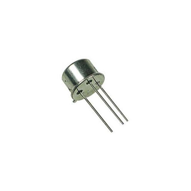
TO-5*
2N3634L, 2N3635L
2N3636L, 2N3637L
* Electrical characteristics for “L” suffix devices are identical to the “non L” corresponding
devices.
** Consult 19500/357 for De-Rating curves.
ELECTRICAL CHARACTERISTICS (TA = +25°C, unless otherwise noted)
Parameters / Test Conditions
Symbol
Min.
V(BR)CEO
140
175
Max.
Unit
OFF CHARACTERTICS
Collector-Emitter Breakdown Voltage
IC = 10mAdc
2N3634, 2N3635
2N3636, 2N3637
Collector-Base Cutoff Current
VCB = 100Vdc
VCB = 140Vdc
VCB = 175Vdc
2N3634, 2N3635
2N3636, 2N3637
ICBO
Vdc
100
10
10
ηAdc
μAdc
μAdc
3 PIN
Emitter-Base Cutoff Current
VEB = 3.0Vdc
VEB = 5.0Vdc
IEBO
50
10
ηAdc
μAdc
Collector-Emitter cutoff Current
VCE = 100Vdc
ICEO
10
μAdc
T4-LDS-0156 Rev. 2 (101452)
TO-39* (TO-205AD)
2N3634, 2N3635
2N3636, 2N3637
2N3634UB, 2N3635UB
2N3636UB, 2N3637UB
Page 1 of 5
�TECHNICAL DATA SHEET
6 Lake Street, Lawrence, MA 01841
1-800-446-1158 / (978) 620-2600 / Fax: (978) 689-0803
Website: http: //www.microsemi.com
Gort Road Business Park, Ennis, Co. Clare, Ireland
Tel: +353 (0) 65 6840044 Fax: +353 (0) 65 6822298
ELECTRICAL CHARACTERISTICS (TA = +25°C, unless otherwise noted)
Parameters / Test Conditions
ON CHARACTERISTICS
Symbol
Min.
Max.
Unit
(1)
Forward-Current Transfer Ratio
IC = 0.1mAdc, VCE = 10Vdc
IC = 1.0mAdc, VCE = 10Vdc
IC = 10mAdc, VCE = 10Vdc
IC = 50mAdc, VCE = 10Vdc
IC = 150mAdc, VCE = 10Vdc
IC = 0.1mAdc, VCE = 10Vdc
IC = 1.0mAdc, VCE = 10Vdc
IC = 10mAdc, VCE = 10Vdc
IC = 50mAdc, VCE = 10Vdc
IC = 150mAdc, VCE = 10Vdc
2N3634, 2N3636
hFE
2N3635, 2N3637
25
45
50
50
30
55
90
100
100
60
Collector-Emitter Saturation Voltage
IC = 10mAdc, IB = 1.0mAdc
IC = 50mAdc, IB = 5.0mAdc
VCE(sat)
Base-Emitter Saturation Voltage
IC = 10mAdc, IB = 1.0mAdc
IC = 50mAdc, IB = 5.0mAdc
VBE(sat)
150
300
0.3
0.6
Vdc
0.65
0.8
0.9
Vdc
Symbol
Min.
Max.
Unit
2N3634, 2N3636
2N3635, 2N3637
|hfe|
1.5
2.0
8.0
8.5
2N3634, 2N3636
2N3635, 2N3637
hfe
40
80
160
320
2N3634, 2N3636
2N3635, 2N3637
hie
100
200
600
1200
Ω
DYNAMIC CHARACTERISTICS
Parameters / Test Conditions
Forward Current Transfer Ratio
IC = 30mAdc, VCE = 30Vdc, f = 100MHz
Forward Current Transfer Ratio
IC = 10mAdc, VCE = 10Vdc, f = 1.0kHz
Small-Signal Short-Circuit Input Impedance
IC = 10mAdc, VCE = 10Vdc, f = 1.0kHz
Small-Signal Open-Circuit Input Impedance
IC = 10mAdc, VCE = 10Vdc, f = 1.0kHz
hoe
200
μs
Output Capacitance
VCB = 20Vdc, IE = 0, 100 kHz ≤ f ≤ 1.0MHz
Cobo
10
pF
Input Capacitance
VEB = 1.0Vdc, IC = 0, 100 kHz ≤ f ≤ 1.0MHz
Cibo
75
pF
Noise Figure
VCE = 10Vdc, IC = 0.5mAdc, Rg = 1.0kΩ
f = 100Hz
f = 1.0kHz
f = 10kHz
NF
5.0
3.0
3.0
dB
(1) Pulse Test: Pulse Width = 300μs, Duty Cycle ≤ 2.0%
T4-LDS-0156 Rev. 2 (101452)
Page 2 of 5
�TECHNICAL DATA SHEET
6 Lake Street, Lawrence, MA 01841
1-800-446-1158 / (978) 620-2600 / Fax: (978) 689-0803
Website: http: //www.microsemi.com
Gort Road Business Park, Ennis, Co. Clare, Ireland
Tel: +353 (0) 65 6840044 Fax: +353 (0) 65 6822298
SAFE OPERATING AREA
DC Tests
TC = 25°C, 1 Cycle, t = 1.0s
Test 1
VCE = 100Vdc, IC = 30mAdc
VCE = 130Vdc, IC = 20mAdc
2N3634, 2N3635
2N3636, 2N3637
Test 2
VCE = 50Vdc, IC = 95mAdc
Test 3
VCE = 5.0Vdc, IC = 1.0Adc
T4-LDS-0156 Rev. 2 (101452)
Page 3 of 5
�TECHNICAL DATA SHEET
6 Lake Street, Lawrence, MA 01841
1-800-446-1158 / (978) 620-2600 / Fax: (978) 689-0803
Website: http: //www.microsemi.com
Gort Road Business Park, Ennis, Co. Clare, Ireland
Tel: +353 (0) 65 6840044 Fax: +353 (0) 65 6822298
PACKAGE DIMENSIONS
Ltr
CD
CH
HD
LC
LD
LL
LU
L1
L2
P
Q
r
TL
TW
α
Term 1
Term 2
Term 3
Dimensions
Millimeters
Min
Max
Min
Max
.305
.335
7.75
8.51
.240
.260
6.10
6.60
.335
.370
8.51
9.40
.200 TYP
5.08 TYP
.016
.021
0.41
0.53
See notes 7, 9, and 10
.016
.019
0.41
0.48
050
1.27
.250
6.35
.100
2.54
.050
1.27
.010
0.254
.029
.045
0.74
1.14
.028
.034
0.71
0.86
45° TP
45° TP
Emitter
Base
Collector
Inches
Notes
7
6
7
7
7
5
8
4
3
6
NOTES:
1. Dimensions are in inches.
2.
Millimeters are given for general information only.
Beyond r maximum, TW must be held to a minimum length of .021 inch (0.53 mm).
3.
4.
TL measured from maximum HD.
CD shall not vary more than ±.010 inch (0.25 mm) in zone P. This zone is controlled for automatic handling.
5.
6.
Leads at gauge plane .054 - .055 inch (1.37 - 1.40 mm) below seating plane shall be within .007 inch (0.18 mm) radius of
true position (TP) at a maximum material condition (MMC) relative to the tab at MMC. The device may be measured by
direct methods or by gauge and gauging procedure.
7.
LU applies between L1 and L2. LD applies between L2 and L minimum. Diameter is uncontrolled in L1 and beyond LL
minimum.
r (radius) applies to both inside corners of tab.
8.
9.
For transistor types 2N3634 through 2N3637, LL is .500 inch (12.70 mm) minimum, and .750 inch (19.05 mm)
maximum (TO-39).
10. For transistor types 2N3634L through 2N3637L, LL is 1.500 inches (38.10 mm) minimum, and 1.750 inches (44.45 mm)
maximum (TO-5).
11. In accordance with ASME Y14.5M, diameters are equivalent to φx symbology.
FIGURE 1: Physical dimensions (TO-5 and TO-39)
T4-LDS-0156 Rev. 2 (101452)
Page 4 of 5
�TECHNICAL DATA SHEET
6 Lake Street, Lawrence, MA 01841
1-800-446-1158 / (978) 620-2600 / Fax: (978) 689-0803
Website: http: //www.microsemi.com
NOTES:
1. Dimensions are in inches.
2. Millimeters are given for general information only.
3. Hatched areas on package denote metallized areas.
4. Pad 1 = Base, Pad 2 = Emitter, Pad 3 = Collector, Pad 4 =
Shielding connected to the lid.
5. In accordance with ASME Y14.5M, diameters are.
equivalent to φx symbology
Gort Road Business Park, Ennis, Co. Clare, Ireland
Tel: +353 (0) 65 6840044 Fax: +353 (0) 65 6822298
Ltr
BH
BL
BW
CL
CW
LL1
LL2
LS1
LS2
LW
r
r1
r2
Inches
Min
.046
.115
.085
.022
.017
.036
.071
.016
Dimensions
Millimeters
Max
Min
Max
.056
1.17
1.42
.128
2.92
3.25
.108
2.16
2.74
.128
3.25
.108
2.74
.038
0.56
0.96
.035
0.43
0.89
.040
0.91
1.02
.079
1.81
2.01
.024
0.41
0.61
.008
.203
.012
.305
.022
.559
Notes
FIGURE 2: Physical dimensions, surface mount 2N3634UB through 2N3637UB (UB version).
T4-LDS-0156 Rev. 2 (101452)
Page 5 of 5
�


 工商网监
湘ICP备2023018690号
工商网监
湘ICP备2023018690号