TECHNICAL DATA
PNP MEDIUM POWER SILICON TRANSISTOR
Qualified per MIL-PRF-19500/561
Devices
Qualified Level
2N6193
JAN, JANTX
JANTXV
MAXIMUM RATINGS
Ratings
Collector-Emitter Voltage
Collector-Base Voltage
Emitter-Base Voltage
Collector Current
Base Current
Total Power Dissipation
@ TA = +250C(1)
@ TC = +250C(2)
Operating & Storage Temperature Range
Symbol
2N6193
Units
VCEO
VCBO
VEBO
IC
IB
100
100
6.0
5.0
1.0
1.0
10
-65 to +200
Vdc
Vdc
Vdc
Adc
Adc
W
W
0
C
PT
Top, Tstg
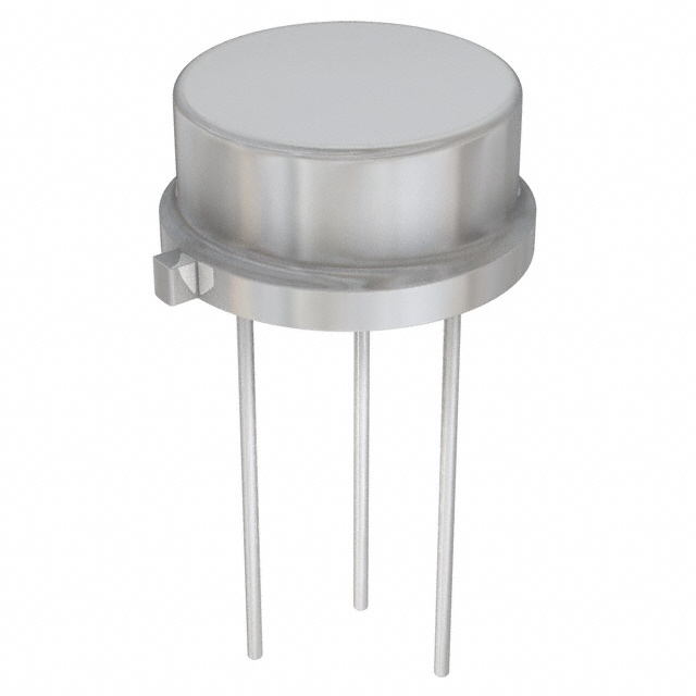
TO-39*
(TO-205AD)
THERMAL CHARACTERISTICS
Characteristics
Thermal Resistance, Junction-to-Case
1) Derate linearly 5.71mW/0C for TA > +250C
2) Derate linearly 57.1mW/0C for TC > +250C
Symbol
RθJC
Max.
17.5
Unit
C/W
0
*See appendix A for
package outline
ELECTRICAL CHARACTERISTICS (TA = 250C unless otherwise noted)
Characteristics
Symbol
Min.
VCEO(sus)
100
Max.
Unit
OFF CHARACTERISTICS
Collector-Emitter Sustaining Voltage
IC = 50 mAdc
Collector-Emitter Cutoff Current
VCE = 100 Vdc
Emitter-Base Cutoff Current
VEB = 6.0 Vdc
Collector-Emitter Cutoff Current
VCE = 90 Vdc, VBE = 1.5 Vdc
Collector-Base Cutoff Current
VCB = 100 Vdc
6 Lake Street, Lawrence, MA 01841
1-800-446-1158 / (978) 794-1666 / Fax: (978) 689-0803
Vdc
ICEO
100
µAdc
IEBO
100
µAdc
ICEX
10
µAdc
ICBO
10
µAdc
120101
Page 1 of 2
�2N6193 JAN SERIES
ELECTRICAL CHARACTERISTICS (con’t)
Characteristics
Symbol
Min.
Max.
hFE
60
60
40
240
Unit
ON CHARACTERISTICS (3)
DC Current Gain
IC = 0.5 Adc, VCE = 2.0 Vdc
IC = 2.0 Adc, VCE = 2.0 Vdc
IC = 5.0 Adc, VCE = 2.0 Vdc
Collector-Emitter Saturation Voltage
IC = 2.0 Adc, IB = 0.2 Adc
IC = 5.0 Adc, IB = 0.5 Adc
Base-Emitter Saturation Voltage
IC = 2.0 Adc, IB = 0.2 Adc
IC = 5.0 Adc, IB = 0.5 Adc
VCE(sat)
0.7
1.2
Vdc
VBE(sat)
1.2
1.8
Vdc
DYNAMIC CHARACTERISTICS
Magnitude of Common Emitter Small-Signal Short Circuit
Forward-Current Transfer Ratio
IC = 0.5 Adc, VCE = 10 Vdc, f = 10 MHz
Output Capacitance
VCB = 10 Vdc, IE = 0, 100 kHz ≤ f ≤ 1.0 MHz
Output Capacitance
VBE = 2.0 Vdc, IC = 0, 100 kHz ≤ f ≤ 1.0 MHz
hfe
3.0
15
Cobo
300
pF
Cibo
1250
pF
100
100
2.0
200
ηs
ηs
µs
ηs
SWITCHING CHARACTERISTICS
Delay Time
Rise Time
Storage Time
Fall Time
VCC = -40 Vdc, VBE(off) = 3.0 Vdc
IC = 2.0 Adc, IB1= 0.2 Adc
VCC = -40 Vdc IC = 2.0 Adc,
IB1 = -IB2 = 0.2 Adc
t
d
r
t
s
t
f
t
SAFE OPERATING AREA
DC Tests
TC = +250C, 1 Cycle, t ≥ 0.5 s
Test 1
VCE = 2.0 Vdc, IC = 5.0 Adc
Test 2
VCE = 90 Vdc, IC = 55 mAdc
(3) Pulse Test: Pulse Width = 300µs, Duty Cycle ≤ 2.0%.
6 Lake Street, Lawrence, MA 01841
1-800-446-1158 / (978) 794-1666 / Fax: (978) 689-0803
120101
Page 2 of 2
�
很抱歉,暂时无法提供与“2N6193”相匹配的价格&库存,您可以联系我们找货
免费人工找货