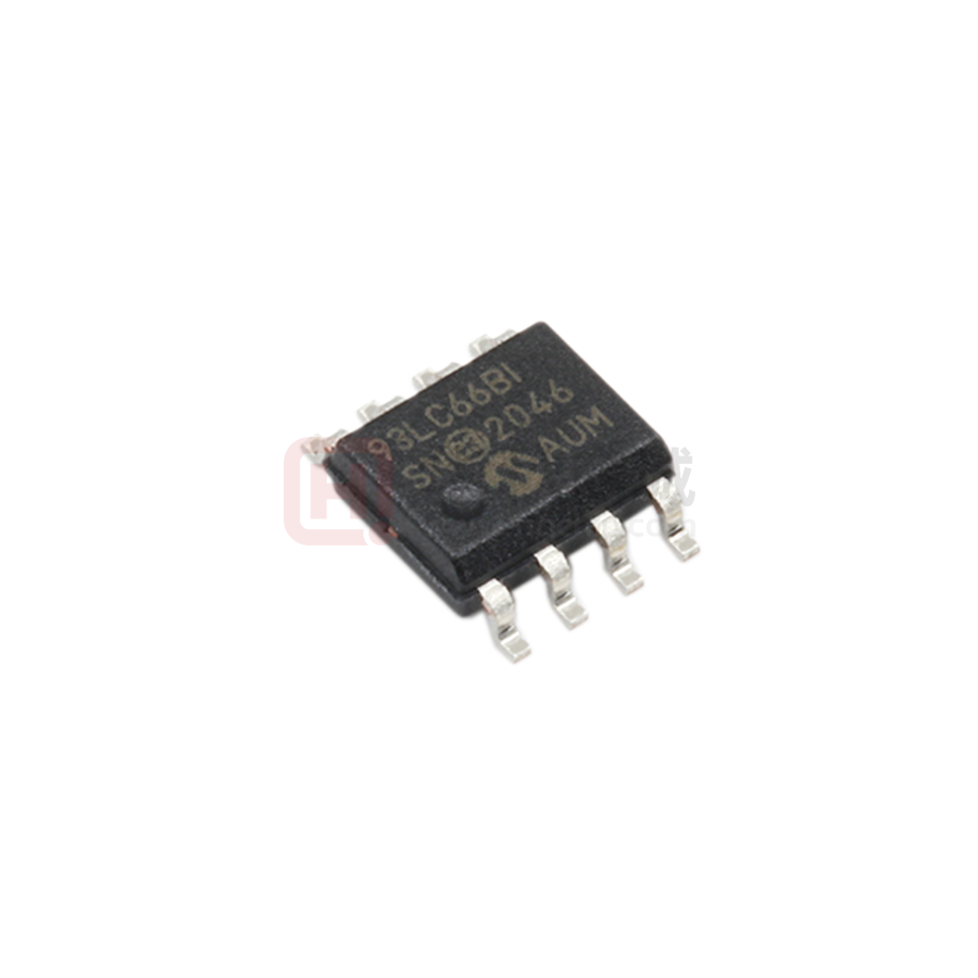
93AA66A/B/C, 93LC66A/B/C,
93C66A/B/C
4K Microwire Compatible Serial EEPROM
Device Selection Table
VCC Range
ORG Pin
Word Size
Temp Ranges
Packages
93AA66A
1.8-5.5
No
8-bit
I
P, SN, ST, MS, OT, MC, MN
93AA66B
1.8-5-5
No
16-bit
I
P, SN, ST, MS, OT, MC, MN
93LC66A
2.5-5.5
No
8-bit
I, E
P, SN, ST, MS, OT, MC, MN
93LC66B
2.5-5.5
No
16-bit
I, E
P, SN, ST, MS, OT, MC, MN
93C66A
4.5-5.5
No
8-bit
I, E
P, SN, ST, MS, OT, MC, MN
93C66B
4.5-5.5
No
16-bit
I, E
P, SN, ST, MS, OT, MC, MN
93AA66C
1.8-5.5
Yes
8- or 16-bit
I
P, SN, ST, MS, MC, MN
Part Number
93LC66C
2.5-5.5
Yes
8- or 16-bit
I, E
P, SN, ST, MS, MC, MN
93C66C
4.5-5.5
Yes
8- or 16-bit
I, E
P, SN, ST, MS, MC, MN
Features:
•
•
•
•
•
•
•
•
•
•
•
•
•
•
Pin Function Table
Low-Power CMOS Technology
ORG Pin to Select Word Size for ‘66C’ Version
512 x 8-bit Organization ‘A’ Devices (no ORG)
256 x 16-bit organization ‘B’ Devices (no ORG)
Self-tImed Erase/Write Cycles (including
Auto-Erase)
Automatic Erase All (ERAL) Before Write All
(WRAL)
Power-On/Off Data Protection Circuitry
Industry Standard 3-Wire Serial I/O
Device Status Signal (Ready/Busy)
Sequential Read Function
1,000,000 Erase/Write Cycles
Data Retention > 200 Years
Pb-free and RoHS Compliant
Temperature Ranges Supported:
- Industrial (I)
-40°C to +85°C
- Automotive (E) -40°C to +125°C
2003-2011 Microchip Technology Inc.
Name
Function
CS
Chip Select
CLK
Serial Data Clock
DI
Serial Data Input
DO
Serial Data Output
VSS
Ground
NC
No internal connection
ORG
Memory Configuration
VCC
Power Supply
Description:
The Microchip Technology Inc. 93XX66A/B/C devices
are 4Kbit low-voltage serial Electrically Erasable
PROMs (EEPROM). Word-selectable devices such as
the 93AA66C, 93LC66C or 93C66C are dependent
upon external logic levels driving the ORG pin to set
word size. For dedicated 8-bit communication, the
93XX66A devices are available, while the 93XX66B
devices provide dedicated 16-bit communication.
Advanced CMOS technology makes these devices
ideal for low-power, nonvolatile memory applications.
The entire 93XX Series is available in standard
packages including 8-lead PDIP and SOIC, and
advanced packaging including 8-lead MSOP, 6-lead
SOT-23, 8-lead 2x3 DFN/TDFN and 8-lead TSSOP. All
packages are Pb-free (Matte Tin) finish.
DS21795E-page 1
�93AA66A/B/C, 93LC66A/B/C, 93C66A/B/C
Package Types (not to scale)
ROTATED SOIC
(ex: 93LC46BX)
NC
VCC
CS
CLK
8 ORG*
7 VSS
6 DO
5 DI
1
2
3
4
PDIP/SOIC
(P, SN)
CS
CLK
DI
DO
TSSOP/MSOP
(ST, MS)
CS
CLK
DI
DO
1
2
3
4
8
7
6
5
1
2
3
4
8
7
6
5
VCC
NC
ORG*
VSS
SOT-23
(OT)
VCC
NC
ORG*
VSS
DO
1
6
VCC
VSS
2
5
CS
DI
3
4
CLK
DFN/TDFN
(MC, MN)
CS
CLK
DI
DO
1
2
3
4
8
7
6
5
VCC
NC
ORG*
VSS
*ORG pin is NC on A/B devices.
DS21795E-page 2
2003-2011 Microchip Technology Inc.
�93AA66A/B/C, 93LC66A/B/C, 93C66A/B/C
1.0
ELECTRICAL CHARACTERISTICS
Absolute Maximum Ratings(†)
VCC.............................................................................................................................................................................7.0V
All inputs and outputs w.r.t. VSS ..........................................................................................................-0.6V to VCC +1.0V
Storage temperature ...............................................................................................................................-65°C to +150°C
Ambient temperature with power applied................................................................................................-40°C to +125°C
ESD protection on all pins 4 kV
† NOTICE: Stresses above those listed under “Absolute Maximum Ratings” may cause permanent damage to the
device. This is a stress rating only and functional operation of the device at those or any other conditions above those
indicated in the operational listings of this specification is not implied. Exposure to maximum rating conditions for
extended periods may affect device reliability.
TABLE 1-1:
DC CHARACTERISTICS
All parameters apply over the specified
ranges unless otherwise noted.
Param.
Symbol
No.
Parameter
Industrial (I):
TA = -40°C to +85°C, VCC = +1.8V to +5.5V
Automotive (E): TA = -40°C to +125°C, VCC = +2.5V to +5.5V
Min
Typ
Max
Units
Conditions
D1
VIH1
VIH2
High-level input voltage
2.0
0.7 VCC
—
—
VCC +1
VCC +1
V
V
VCC 2.7V
VCC < 2.7V
D2
VIL1
VIL2
Low-level input voltage
-0.3
-0.3
—
—
0.8
0.2 VCC
V
V
VCC 2.7V
VCC < 2.7V
D3
VOL1
VOL2
Low-level output voltage
—
—
—
—
0.4
0.2
V
V
IOL = 2.1 mA, VCC = 4.5V
IOL = 100 A, VCC = 2.5V
D4
VOH1
VOH2
High-level output voltage
2.4
VCC - 0.2
—
—
—
—
V
V
IOH = -400 A, VCC = 4.5V
IOH = -100 A, VCC = 2.5V
D5
ILI
Input leakage current
—
—
±1
A
VIN = VSS or VCC
D6
ILO
Output leakage current
—
—
±1
A
VOUT = VSS or VCC
D7
CIN,
COUT
Pin capacitance (all inputs/
outputs)
—
—
7
pF
VIN/VOUT = 0V (Note 1)
TA = 25°C, FCLK = 1 MHz
D8
ICC write Write current
—
—
—
500
2
—
mA
A
FCLK = 3 MHz, Vcc = 5.5V
FCLK = 2 MHz, Vcc = 2.5V
D9
ICC read Read current
—
—
—
—
—
100
1
500
—
mA
A
A
FCLK = 3 MHz, VCC = 5.5V
FCLK = 2 MHz, VCC = 3.0V
FCLK = 2 MHz, VCC = 2.5V
D10
ICCS
Standby current
—
—
—
—
1
5
A
A
I – Temp
E – Temp
CLK = Cs = 0V
ORG = DI = VSS or VCC
(Note 2) (Note 3)
D11
VPOR
VCC voltage detect
93AA66A/B/C, 93LC66A/B/C
93C66A/B/C
—
—
1.5V
3.8V
—
—
V
V
(Note 1)
Note 1:
2:
3:
This parameter is periodically sampled and not 100% tested.
ORG pin not available on ‘A’ or ‘B’ versions.
Ready/Busy status must be cleared from DO; see Section 3.4 "Data Out (DO)".
2003-2011 Microchip Technology Inc.
DS21795E-page 3
�93AA66A/B/C, 93LC66A/B/C, 93C66A/B/C
TABLE 1-2:
AC CHARACTERISTICS
All parameters apply over the specified
ranges unless otherwise noted.
Param.
Symbol
No.
Parameter
Industrial (I):
TA = -40°C to +85°C, VCC = +1.8V to +5.5V
Automotive (E): TA = -40°C to +125°C, VCC = +2.5V to +5.5V
Min
Max
Units
Conditions
A1
FCLK
Clock frequency
—
3
2
1
MHz
MHz
MHz
4.5V VCC < 5.5V, 93XX66C only
2.5V VCC < 5.5V
1.8V VCC < 2.5V
A2
TCKH
Clock high time
200
250
450
—
ns
ns
ns
4.5V VCC < 5.5V, 93XX66C only
2.5V VCC < 5.5V
1.8V VCC < 2.5V
A3
TCKL
Clock low time
100
200
450
—
ns
ns
ns
4.5V VCC < 5.5V, 93XX66C only
2.5V VCC < 5.5V
1.8V VCC < 2.5V
A4
TCSS
Chip Select setup time
50
100
250
—
ns
ns
ns
4.5V VCC < 5.5V
2.5V VCC < 4.5V
1.8V VCC < 2.5V
A5
TCSH
Chip Select hold time
0
—
ns
1.8V VCC < 5.5V
A6
TCSL
Chip Select low time
250
—
ns
1.8V VCC < 5.5V
A7
TDIS
Data input setup time
50
100
250
—
ns
ns
ns
4.5V VCC < 5.5V, 93XX66C only
2.5V VCC < 5.5V
1.8V VCC < 2.5V
A8
TDIH
Data input hold time
50
100
250
—
ns
ns
ns
4.5V VCC < 5.5V, 93XX66C only
2.5V VCC < 5.5V
1.8V VCC < 2.5V
A9
TPD
Data output delay time
—
200
250
400
ns
ns
ns
4.5V VCC < 5.5V, CL = 100 pF
2.5V VCC < 4.5V, CL = 100 pF
1.8V VCC < 2.5V, CL = 100 pF
A10
TCZ
Data output disable time
—
100
200
ns
ns
4.5V VCC < 5.5V, (Note 1)
1.8V VCC < 4.5V, (Note 1)
A11
TSV
Status valid time
—
200
300
500
ns
ns
ns
4.5V VCC < 5.5V, CL = 100 pF
2.5V VCC < 4.5V, CL = 100 pF
1.8V VCC < 2.5V, CL = 100 pF
A12
TWC
Program cycle time
—
6
ms
Erase/Write mode (AA and LC
versions)
A13
TWC
—
2
ms
Erase/Write mode
(93C versions)
A14
TEC
—
6
ms
ERAL mode, 4.5V VCC 5.5V
A15
TWL
—
15
ms
WRAL mode, 4.5V VCC 5.5V
A16
—
1M
—
Note 1:
2:
Endurance
cycles 25°C, VCC = 5.0V, (Note 2)
This parameter is periodically sampled and not 100% tested.
This application is not tested but ensured by characterization. For endurance estimates in a specific
application, please consult the Total Endurance™ Model, which may be obtained from Microchip’s web
site at www.microchip.com.
DS21795E-page 4
2003-2011 Microchip Technology Inc.
�93AA66A/B/C, 93LC66A/B/C, 93C66A/B/C
FIGURE 1-1:
CS
SYNCHRONOUS DATA TIMING
VIH
TCSS
VIL
CLK
TCKH
TCKL
TCSH
VIH
VIL
TDIS
DI
TDIH
VIH
VIL
DO
(Read)
DO
(Program)
VOH
VOL
VOH
TPD
TPD
TCZ
TCZ
TSV
Status Valid
VOL
Note: TSV is relative to CS.
TABLE 1-3: INSTRUCTION SET FOR X16 ORGANIZATION (93XX66B OR 93XX66C WITH ORG = 1)
Instruction
SB
Opcode
Address
A7 A6 A5 A4 A3 A2 A1 A0
Data In
Data Out
Req. CLK Cycles
ERASE
1
11
—
(RDY/BSY)
11
ERAL
1
00
1
0
X
X
X
X
X
X
—
(RDY/BSY)
11
EWDS
1
00
0
0
X
X
X
X
X
X
—
High-Z
11
EWEN
1
00
1
1
X
X
X
X
X
X
—
High-Z
11
READ
1
10
A7 A6 A5 A4 A3 A2 A1 A0
—
D15 – D0
27
WRITE
1
01
A7 A6 A5 A4 A3 A2 A1 A0
D15 – D0
(RDY/BSY)
27
WRAL
1
00
D15 – D0
(RDY/BSY)
27
0
1
X
X
X
X
X
X
TABLE 1-4: INSTRUCTION SET FOR X8 ORGANIZATION (93XX66A OR 93XX66C WITH ORG = 0)
SB
Opcode
Address
Data In
Data Out
Req. CLK
Cycles
ERASE
1
11
A8 A7 A6 A5 A4 A3 A2 A1 A0
—
(RDY/BSY)
12
ERAL
1
00
1
0
X
X
X
X
X
X
X
—
(RDY/BSY)
12
EWDS
1
00
0
0
X
X
X
X
X
X
X
—
High-Z
12
EWEN
1
00
1
1
X
X
X
X
X
X
X
—
High-Z
12
READ
1
10
A8 A7 A6 A5 A4 A3 A2 A1 A0
—
D7 – D0
20
WRITE
1
01
A8 A7 A6 A5 A4 A3 A2 A1 A0
D7 – D0
(RDY/BSY)
20
WRAL
1
00
D7 – D0
(RDY/BSY)
20
Instruction
0
2003-2011 Microchip Technology Inc.
1
X
X
X
X
X
X
X
DS21795E-page 5
�93AA66A/B/C, 93LC66A/B/C, 93C66A/B/C
2.0
FUNCTIONAL DESCRIPTION
2.2
Data In/Data Out (DI/DO)
When the ORG pin is connected to VCC, the (x16) organization is selected. When it is connected to ground,
the (x8) organization is selected. Instructions,
addresses and write data are clocked into the DI pin on
the rising edge of the clock (CLK). The DO pin is
normally held in a High-Z state except when reading
data from the device, or when checking the Ready/
Busy status during a programming operation. The
Ready/Busy status can be verified during an Erase/
Write operation by polling the DO pin; DO low indicates
that programming is still in progress, while DO high
indicates the device is ready. DO will enter the High-Z
state on the falling edge of CS.
It is possible to connect the Data In and Data Out pins
together. However, with this configuration it is possible
for a “bus conflict” to occur during the “dummy zero”
that precedes the read operation, if A0 is a logic high
level. Under such a condition the voltage level seen at
Data Out is undefined and will depend upon the relative
impedances of Data Out and the signal source driving
A0. The higher the current sourcing capability of A0,
the higher the voltage at the Data Out pin. In order to
limit this current, a resistor should be connected
between DI and DO.
2.1
All modes of operation are inhibited when VCC is below
a typical voltage of 1.5V for ‘93AA’ and ‘93LC’ devices
or 3.8V for ‘93C’ devices.
Start Condition
The Start bit is detected by the device if CS and DI are
both high with respect to the positive edge of CLK for
the first time.
Before a Start condition is detected, CS, CLK and DI
may change in any combination (except to that of a
Start condition), without resulting in any device
operation (Read, Write, Erase, EWEN, EWDS, ERAL
or WRAL). As soon as CS is high, the device is no
longer in Standby mode.
An instruction following a Start condition will only be
executed if the required opcode, address and data bits
for any particular instruction are clocked in.
Note:
When preparing to transmit an instruction,
either the CLK or DI signal levels must be
at a logic low as CS is toggled active high.
2.3
Data Protection
The EWEN and EWDS commands give additional
protection against accidentally programming during
normal operation.
Note:
For added protection, an EWDS command
should be performed after every write
operation.
After power-up, the device is automatically in the
EWDS mode. Therefore, an EWEN instruction must be
performed before the initial ERASE or WRITE instruction
can be executed.
Block Diagram
VCC
VSS
Memory
Array
Address
Decoder
Address
Counter
Data Register
Output
Buffer
DO
DI
ORG*
CS
CLK
Mode
Decode
Logic
Clock
Register
*ORG input is not available on A/B devices
DS21795E-page 6
2003-2011 Microchip Technology Inc.
�93AA66A/B/C, 93LC66A/B/C, 93C66A/B/C
2.4
Erase
The DO pin indicates the Ready/Busy status of the
device if CS is brought high after a minimum of 250 ns
low (TCSL). DO at logical ‘0’ indicates that programming
is still in progress. DO at logical ‘1’ indicates that the
register at the specified address has been erased and
the device is ready for another instruction.
The ERASE instruction forces all data bits of the specified address to the logical ‘1’ state. CS is brought low
following the loading of the last address bit. This falling
edge of the CS pin initiates the self-timed programming cycle, except on ‘93C’ devices where the rising
edge of CLK before the last address bit initiates the
write cycle.
FIGURE 2-1:
Note:
Issuing a Start bit and then taking CS low
will clear the Ready/Busy status from DO.
ERASE TIMING FOR 93AA AND 93LC DEVICES
TCSL
CS
Check Status
CLK
1
DI
1
1
AN
AN-1 AN-2
•••
A0
TCZ
TSV
DO
High-Z
Busy
Ready
High-Z
TWC
FIGURE 2-2:
ERASE TIMING FOR 93C DEVICES
TCSL
CS
Check Status
CLK
1
DI
1
1
AN
AN-1 AN-2
•••
A0
TCZ
TSV
DO
High-Z
Busy
Ready
High-Z
TWC
2003-2011 Microchip Technology Inc.
DS21795E-page 7
�93AA66A/B/C, 93LC66A/B/C, 93C66A/B/C
2.5
Erase All (ERAL)
The DO pin indicates the Ready/Busy status of the
device, if CS is brought high after a minimum of 250 ns
low (TCSL).
The Erase All (ERAL) instruction will erase the entire
memory array to the logical ‘1’ state. The ERAL cycle
is identical to the erase cycle, except for the different
opcode. The ERAL cycle is completely self-timed and
commences at the falling edge of the CS, except on
‘93C’ devices where the rising edge of CLK before the
last data bit initiates the write cycle. Clocking of the
CLK pin is not necessary after the device has entered
the ERAL cycle.
FIGURE 2-3:
Note:
Issuing a Start bit and then taking CS low
will clear the Ready/Busy status from DO.
VCC must be 4.5V for proper operation of ERAL.
ERAL TIMING FOR 93AA AND 93LC DEVICES
TCSL
CS
Check Status
CLK
DI
1
0
0
1
0
x
•••
x
TCZ
TSV
DO
High-Z
Busy
Ready
High-Z
TEC
VCC must be 4.5V for proper operation of ERAL.
FIGURE 2-4:
ERAL TIMING FOR 93C DEVICES
TCSL
CS
Check Status
CLK
DI
1
0
0
1
0
x
•••
x
TCZ
TSV
DO
High-Z
Busy
Ready
High-Z
TEC
DS21795E-page 8
2003-2011 Microchip Technology Inc.
�93AA66A/B/C, 93LC66A/B/C, 93C66A/B/C
2.6
Erase/Write Disable and Enable
(EWDS/EWEN)
To protect against accidental data disturbance, the
EWDS instruction can be used to disable all erase/write
functions and should follow all programming operations. Execution of a READ instruction is independent of
both the EWEN and EWDS instructions.
The 93XX66A/B/C powers up in the Erase/Write
Disable (EWDS) state. All Programming modes must be
preceded by an Erase/Write Enable (EWEN) instruction.
Once the EWEN instruction is executed, programming
remains enabled until an EWDS instruction is executed
or Vcc is removed from the device.
FIGURE 2-5:
EWDS TIMING
TCSL
CS
CLK
DI
1
FIGURE 2-6:
0
0
0
0
•••
x
x
EWEN TIMING
TCSL
CS
CLK
1
DI
2.7
0
0
1
1
•••
x
Read
the rising edge of the CLK and are stable after the
specified time delay (TPD). Sequential read is possible
when CS is held high. The memory data will
automatically cycle to the next register and output
sequentially.
The READ instruction outputs the serial data of the
addressed memory location on the DO pin. A dummy
zero bit precedes the 8-bit (If ORG pin is low or A-Version
devices) or 16-bit (If ORG pin is high or B-version
devices) output string. The output data bits will toggle on
FIGURE 2-7:
x
READ TIMING
CS
CLK
DI
DO
1
1
0
High-Z
2003-2011 Microchip Technology Inc.
An
•••
A0
0
Dx
•••
D0
Dx
•••
D0
Dx
•••
D0
DS21795E-page 9
�93AA66A/B/C, 93LC66A/B/C, 93C66A/B/C
2.8
Write
The DO pin indicates the Ready/Busy status of the
device, if CS is brought high after a minimum of 250 ns
low (TCSL). DO at logical ‘0’ indicates that programming
is still in progress. DO at logical ‘1’ indicates that the
register at the specified address has been written with
the data specified and the device is ready for another
instruction.
The WRITE instruction is followed by 8 bits (If ORG is
low or A-version devices) or 16 bits (If ORG pin is high
or B-version devices) of data which are written into the
specified address. For 93AA66A/B/C and 93LC66A/B/C
devices, after the last data bit is clocked into DI, the
falling edge of CS initiates the self-timed auto-erase and
programming cycle. For 93C66A/B/C devices, the selftimed auto-erase and programming cycle is initiated by
the rising edge of CLK on the last data bit.
FIGURE 2-8:
Note:
Issuing a Start bit and then taking CS low
will clear the Ready/Busy status from DO.
WRITE TIMING FOR 93AA AND 93LC DEVICES
TCSL
CS
CLK
DI
1
0
1
AN
•••
A0
Dx
•••
D0
TSV
High-Z
DO
Busy
TCZ
Ready
High-Z
TWC
FIGURE 2-9:
WRITE TIMING FOR 93C DEVICES
TCSL
CS
CLK
DI
1
0
1
AN
•••
A0
Dx
•••
D0
TSV
DO
High-Z
Busy
TCZ
Ready
High-Z
TWC
DS21795E-page 10
2003-2011 Microchip Technology Inc.
�93AA66A/B/C, 93LC66A/B/C, 93C66A/B/C
2.9
Write All (WRAL)
The DO pin indicates the Ready/Busy status of the
device if CS is brought high after a minimum of 250 ns
low (TCSL).
The Write All (WRAL) instruction will write the entire
memory array with the data specified in the command.
For 93AA66A/B/C and 93LC66A/B/C devices, after the
last data bit is clocked into DI, the falling edge of CS
initiates the self-timed auto-erase and programming
cycle. For 93C66A/B/C devices, the self-timed autoerase and programming cycle is initiated by the rising
edge of CLK on the last data bit. Clocking of the CLK
pin is not necessary after the device has entered the
WRAL cycle. The WRAL command does include an
automatic ERAL cycle for the device. Therefore, the
WRAL instruction does not require an ERAL instruction,
but the chip must be in the EWEN status.
FIGURE 2-10:
Note:
Issuing a Start bit and then taking CS low
will clear the Ready/Busy status from DO.
VCC must be 4.5V for proper operation of WRAL.
WRAL TIMING FOR 93AA AND 93LC DEVICES
TCSL
CS
CLK
DI
1
0
0
0
1
x
•••
x
Dx
•••
D0
TSV
High-Z
DO
Busy
TCZ
Ready
HIGH-Z
TWL
VCC must be 4.5V for proper operation of WRAL.
FIGURE 2-11:
WRAL TIMING FOR 93C DEVICES
TCSL
CS
CLK
DI
1
0
0
0
1
x
•••
x
Dx
•••
D0
TSV
DO
High-Z
Busy
TCZ
Ready
HIGH-Z
TWL
2003-2011 Microchip Technology Inc.
DS21795E-page 11
�93AA66A/B/C, 93LC66A/B/C, 93C66A/B/C
3.0
PIN DESCRIPTIONS
TABLE 3-1:
PIN DESCRIPTIONS
PDIP
SOIC
TSSOP
MSOP
DFN(1)
TDFN(1)
SOT-23
Rotated
SOIC
CS
1
1
1
1
1
1
5
3
Chip Select
CLK
2
2
2
2
2
2
4
4
Serial Clock
Name
Function
DI
3
3
3
3
3
3
3
5
Data In
DO
4
4
4
4
4
4
1
6
Data Out
VSS
5
5
5
5
5
5
2
7
Ground
ORG/NC
6
6
6
6
6
6
N/A
8
Organization / 93XX66C
No Internal Connection /
93XX66A/B
NC
7
7
7
7
7
7
N/A
1
No Internal Connection
VCC
8
8
8
8
8
8
6
2
Power Supply
Note 1:
3.1
The exposed pad on the DFN/TDFN package may be connected to VSS or left floating.
Chip Select (CS)
A high level selects the device; a low level deselects
the device and forces it into Standby mode. However, a
programming cycle which is already in progress will be
completed, regardless of the Chip Select (CS) input
signal. If CS is brought low during a program cycle, the
device will go into Standby mode as soon as the
programming cycle is completed.
CS must be low for 250 ns minimum (TCSL) between
consecutive instructions. If CS is low, the internal
control logic is held in a Reset status.
3.2
Serial Clock (CLK)
data bits before an instruction is executed. CLK and DI
then become “don’t care” inputs waiting for a new Start
condition to be detected.
3.3
Data In (DI)
Data In (DI) is used to clock in a Start bit, opcode,
address and data synchronously with the CLK input.
3.4
Data Out (DO)
Data Out (DO) is used in the Read mode to output data
synchronously with the CLK input (TPD after the positive edge of CLK).
The Serial Clock is used to synchronize the communication between a master device and the 93XX series
device. Opcodes, address and data bits are clocked in
on the positive edge of CLK. Data bits are also clocked
out on the positive edge of CLK.
This pin also provides Ready/Busy status information
during erase and write cycles. Ready/Busy status information is available on the DO pin if CS is brought high
after being low for minimum Chip Select Low Time
(TCSL) and an erase or write operation has been
initiated.
CLK can be stopped anywhere in the transmission
sequence (at high or low level) and can be continued
anytime with respect to Clock High Time (TCKH) and
Clock Low Time (TCKL). This gives the controlling
master freedom in preparing opcode, address and
data.
The Status signal is not available on DO, if CS is held
low during the entire erase or write cycle. In this case,
DO is in the High-Z mode. If status is checked after the
erase/write cycle, the data line will be high to indicate
the device is ready.
CLK is a “don’t care” if CS is low (device deselected). If
CS is high, but the Start condition has not been
detected (DI = 0), any number of clock cycles can be
received by the device without changing its status (i.e.,
waiting for a Start condition).
3.5
CLK cycles are not required during the self-timed write
(i.e., auto erase/write) cycle.
After detection of a Start condition the specified number
of clock cycles (respectively low-to-high transitions of
CLK) must be provided. These clock cycles are
required to clock in all required opcode, address and
DS21795E-page 12
Note:
Issuing a Start bit and then taking CS low
will clear the Ready/Busy status from DO.
Organization (ORG)
When the ORG pin is connected to VCC or Logic HI, the
(x16) memory organization is selected. When the ORG
pin is tied to VSS or Logic LO, the (x8) memory
organization is selected. For proper operation, ORG
must be tied to a valid logic level.
93XX66A devices are always (x8) organization and
93XX66B devices are always (x16) organization.
2003-2011 Microchip Technology Inc.
�93AA66A/B/C, 93LC66A/B/C, 93C66A/B/C
4.0
PACKAGING INFORMATION
4.1
Package Marking Information
8-Lead MSOP (150 mil)
XXXXXXT
YWWNNN
6-Lead SOT-23
XXNN
8-Lead PDIP
Example:
3L66BI
5281L7
Example:
3EL7
Example:
XXXXXXXX
T/XXXNNN
YYWW
93LC66B
I/P e3 1L7
0528
8-Lead SOIC
Example:
XXXXXXXT
XXXXYYWW
NNN
93LC66BI
SN e3 0528
1L7
8-Lead TSSOP
Example:
XXXX
TYWW
NNN
8-Lead 2x3 DFN
XXX
YWW
NN
8-Lead 2x3 TDFN
XXX
YWW
NN
2003-2011 Microchip Technology Inc.
L66B
I528
1L7
Example:
374
528
L7
Example:
E74
528
L7
DS21795E-page 13
�93AA66A/B/C, 93LC66A/B/C, 93C66A/B/C
1st Line Marking Codes
Part Number
93AA66A
TSSOP
MSOP
A66A
SOT-23
DFN
TDFN
I Temp.
E Temp.
I Temp.
E Temp.
I Temp.
E Temp.
3A66AT
3BNN
—
361
—
E61
—
93AA66B
A66B
3A66BT
3LNN
—
371
—
E71
—
93AA66C
A66C
3A66CT
—
—
381
—
E81
—
93LC66A
L66A
3L66AT
3ENN
3FNN
364
—
E64
E65
93LC66B
L66B
3L66BT
3PNN
3RNN
374
—
E74
E75
93LC66C
L66C
3L66CT
—
—
384
—
E84
E85
93C66A
C66A
3C66AT
3HNN
3JNN
367
—
E67
E68
93C66B
C66B
3C66BT
3TNN
3UNN
377
—
E77
E78
93C66C
C66C
3C66CT
—
—
387
—
E87
E88
Note:
T = Temperature grade (I, E)
NN = Alphanumeric traceability code
Legend: XX...X
T
Y
YY
WW
NNN
e3
Part number or part number code
Temperature (I, E)
Year code (last digit of calendar year)
Year code (last 2 digits of calendar year)
Week code (week of January 1 is week ‘01’)
Alphanumeric traceability code (2 characters for small packages)
Pb-free JEDEC designator for Matte Tin (Sn)
Note:
For very small packages with no room for the Pb-free JEDEC designator
e3 , the marking will only appear on the outer carton or reel label.
Note:
In the event the full Microchip part number cannot be marked on one line, it will
be carried over to the next line, thus limiting the number of available
characters for customer-specific information.
DS21795E-page 14
2003-2011 Microchip Technology Inc.
�93AA66A/B/C, 93LC66A/B/C, 93C66A/B/C
Note:
For the most current package drawings, please see the Microchip Packaging Specification located at
http://www.microchip.com/packaging
2003-2011 Microchip Technology Inc.
DS21795E-page 15
�93AA66A/B/C, 93LC66A/B/C, 93C66A/B/C
Note:
For the most current package drawings, please see the Microchip Packaging Specification located at
http://www.microchip.com/packaging
DS21795E-page 16
2003-2011 Microchip Technology Inc.
�93AA66A/B/C, 93LC66A/B/C, 93C66A/B/C
Note:
For the most current package drawings, please see the Microchip Packaging Specification located at
http://www.microchip.com/packaging
2003-2011 Microchip Technology Inc.
DS21795E-page 17
�93AA66A/B/C, 93LC66A/B/C, 93C66A/B/C
�������
���
�����
����
��������
������������������
�����
.
�#����
#��$ ��#����/����! �-��� 0����� �� ���#������
�����1��/�����������%���#�
���
��#�!��#�
�##�+22---����
������
�2���/�����
b
4
N
E
E1
PIN 1 ID BY
LASER MARK
1
2
3
e
e1
D
A
A2
c
φ
L
A1
L1
3��#
����� �
��4���#
5$�8� �
%�1��
��44��"
"��
��5
5
56�
��7
9
1�#��
�
���(�)�*
6$# �!��4��!�1�#��
��
�����)�*
6,� ����:����#
�
����
;
�
�!�!�1��/����
���/��
��
��