v5.3
SX-A Family FPGAs
™
u e
Leading-Edge Performance
•
•
•
250 MHz System Performance
350 MHz Internal Performance
•
•
•
Specifications
•
•
•
•
•
•
12,000 to 108,000 Available System Gates
Up to 360 User-Programmable I/O Pins
Up to 2,012 Dedicated Flip-Flops
0.22 μ / 0.25 μ CMOS Process Technology
•
•
Features
•
•
•
•
•
Hot-Swap Compliant I/Os
Power-Up/Down Friendly (No Sequencing Required
for Supply Voltages)
66 MHz PCI Compliant
Nonvolatile, Single-Chip Solution
•
Configurable I/O Support for 3.3 V / 5 V PCI, 5 V
TTL, 3.3 V LVTTL, 2.5 V LVCMOS2
2.5 V, 3.3 V, and 5 V Mixed-Voltage Operation with
5 V Input Tolerance and 5 V Drive Strength
Devices Support Multiple Temperature Grades
Configurable Weak-Resistor Pull-Up or Pull-Down
for I/O at Power-Up
Individual Output Slew Rate Control
Up to 100% Resource Utilization and 100% Pin
Locking
Deterministic, User-Controllable Timing
Unique In-System Diagnostic and Verification
Capability with Silicon Explorer II
Boundary-Scan Testing in Compliance with IEEE
Standard 1149.1 (JTAG)
Actel Secure Programming Technology with
FuseLock™ Prevents Reverse Engineering and
Design Theft
Table 1 • SX-A Product Profile
Device
Capacity
Typical Gates
System Gates
Logic Modules
Combinatorial Cells
Dedicated Flip-Flops
Maximum Flip-Flops
Maximum User I/Os
Global Clocks
Quadrant Clocks
A54SX08A
A54SX16A
A54SX32A
A54SX72A
8,000
12,000
16,000
24,000
32,000
48,000
72,000
108,000
768
512
256
512 1
1,452
924
528
990
2,880
1,800
1,080
1,980
6,036
4,024
2,012
4,024
130
180
249
360
3
3
3
3
0
0
0
4
Boundary Scan Testing
Yes
Yes
Yes
Yes
3.3 V / 5 V PCI
Yes
Yes
Yes
Yes
Input Set-Up (External)
0 ns
0 ns
0 ns
0 ns
–F, Std, –1, –2
–F, Std, –1, –2, –3
–F, Std, –1, –2, –3
–F, Std, –1, –2, –3
Temperature Grades
C, I, A, M
C, I, A, M
C, I, A, M
C, I, A, M
Package (by pin count)
PQFP
TQFP
PBGA
FBGA
CQFP
208
100, 144
–
144
–
208
100, 144
–
144, 256
–
208
100, 144, 176
329
144, 256, 484
208, 256
208
–
–
256, 484
208, 256
Speed Grades2
Notes:
1. A maximum of 512 registers is possible if all 512 C cells are used to build an additional 256 registers.
2. All –3 speed grades have been discontinued.
February 2007
© 2007 Actel Corporation
i
See the Actel website for the latest version of the datasheet.
�SX-A Family FPGAs
Ordering Information
A54SX16A
2
PQ
G
208
Application (Temperature Range)
Blank = Commercial (0 to +70°)
I = Industrial (-40 to +85°C)
A = Automotive (-40 to +125°C)
M = Military (-55 to +125°C)
B = MIL-STD-883 Class B
Package Lead Count
Lead-Free Packaging
Blank = Standard Packaging
G = RoHS Compliant Packaging
Package Type
BG = 1.27 mm Plastic Ball Grid Array
FG = 1.0 mm Fine Pitch Ball Grid Array
PQ = Plastic Quad Flat Pack
TQ = Thin (1.4 mm) Quad Flat Pack
CQ = Ceramic Quad Flat Pack1
Speed Grade
Blank = Standard Speed
–1 = Approximately 15% Faster than Standard
–2 = Approximately 25% Faster than Standard
–3 = Approximately 35% Faster than Standard2
–F = Approximately 40% Slower than Standard
Part Number
A54SX08A = 12,000 System Gates
A54SX16A = 24,000 System Gates
A54SX32A = 48,000 System Gates
A54SX72A = 108,000 System Gates
Notes:
1. For more information about the CQFP package options, refer to the HiRel SX-A datasheet.
2. All –3 speed grades have been discontinued.
Device Resources
User I/Os (Including Clock Buffers)
208-Pin
PQFP
100-Pin
TQFP
144-Pin
TQFP
176-Pin
TQFP
329-Pin
PBGA
144-Pin
FBGA
256-Pin
FBGA
484-Pin
FBGA
A54SX08A
130
81
113
–
–
111
–
–
A54SX16A
175
81
113
–
–
111
180
–
A54SX32A
174
81
113
147
249
111
203
249
A54SX72A
171
–
–
–
–
–
203
360
Device
Notes: Package Definitions: PQFP = Plastic Quad Flat Pack, TQFP = Thin Quad Flat Pack, PBGA = Plastic Ball Grid Array,
FBGA = Fine Pitch Ball Grid Array
ii
v5.3
�SX-A Family FPGAs
Temperature Grade Offering
Package
A54SX08A
A54SX16A
A54SX32A
A54SX72A
C,I,A,M
PQ208
C,I,A,M
C,I,A,M
C,I,A,M
TQ100
C,I,A,M
C,I,A,M
C,I,A,M
TQ144
C,I,A,M
C,I,A,M
C,I,A,M
TQ176
C,I,M
BG329
C,I,M
FG144
C,I,A,M
C,I,A,M
C,I,A,M
C,I,A,M
C,I,A,M
C,I,A,M
FG484
C,I,M
C,I,A,M
CQ208
C,M,B
C,M,B
CQ256
C,M,B
C,M,B
FG256
Notes:
1.
2.
3.
4.
5.
6.
7.
C = Commercial
I = Industrial
A = Automotive
M = Military
B = MIL-STD-883 Class B
For more information regarding automotive products, refer to the SX-A Automotive Family FPGAs datasheet.
For more information regarding Mil-Temp and ceramic packages, refer to the HiRel SX-A Family FPGAs datasheet.
Speed Grade and Temperature Grade Matrix
F
–1
–2
–3
✓
✓
✓
Discontinued
Industrial
✓
✓
✓
Discontinued
Automotive
✓
Military
✓
✓
MIL-STD-883B
✓
✓
Commercial
✓
Std
Notes:
1. For more information regarding automotive products, refer to the SX-A Automotive Family FPGAs datasheet.
2. For more information regarding Mil-Temp and ceramic packages, refer to the HiRel SX-A Family FPGAs datasheet.
Contact your Actel Sales representative for more information on availability.
v5.3
iii
�SX-A Family FPGAs
Table of Contents
General Description
Introduction . . . . . . . . . . . . . . . . . . . . . . . . . . . . . . . . . . . . . . . . . . . . . . . . . . . . . . . . 1-1
SX-A Family Architecture . . . . . . . . . . . . . . . . . . . . . . . . . . . . . . . . . . . . . . . . . . . . . . 1-1
Other Architectural Features . . . . . . . . . . . . . . . . . . . . . . . . . . . . . . . . . . . . . . . . . . . 1-7
Programming . . . . . . . . . . . . . . . . . . . . . . . . . . . . . . . . . . . . . . . . . . . . . . . . . . . . . . 1-13
Related Documents . . . . . . . . . . . . . . . . . . . . . . . . . . . . . . . . . . . . . . . . . . . . . . . . . 1-14
Pin Description . . . . . . . . . . . . . . . . . . . . . . . . . . . . . . . . . . . . . . . . . . . . . . . . . . . . . 1-15
Detailed Specifications
Operating Conditions
. . . . . . . . . . . . . . . . . . . . . . . . . . . . . . . . . . . . . . . . . . . . . . 2-1
Typical SX-A Standby Current
Electrical Specifications
. . . . . . . . . . . . . . . . . . . . . . . . . . . . . . . . . . . . . . . . . 2-1
. . . . . . . . . . . . . . . . . . . . . . . . . . . . . . . . . . . . . . . . . . . . . 2-2
PCI Compliance for the SX-A Family . . . . . . . . . . . . . . . . . . . . . . . . . . . . . . . . . . . . . 2-3
Thermal Characteristics . . . . . . . . . . . . . . . . . . . . . . . . . . . . . . . . . . . . . . . . . . . . . . 2-11
SX-A Timing Model . . . . . . . . . . . . . . . . . . . . . . . . . . . . . . . . . . . . . . . . . . . . . . . . . . 2-14
Sample Path Calculations . . . . . . . . . . . . . . . . . . . . . . . . . . . . . . . . . . . . . . . . . . . . . 2-14
Output Buffer Delays . . . . . . . . . . . . . . . . . . . . . . . . . . . . . . . . . . . . . . . . . . . . . . . . 2-15
AC Test Loads . . . . . . . . . . . . . . . . . . . . . . . . . . . . . . . . . . . . . . . . . . . . . . . . . . . . . . 2-15
Input Buffer Delays . . . . . . . . . . . . . . . . . . . . . . . . . . . . . . . . . . . . . . . . . . . . . . . . . . 2-16
C-Cell Delays . . . . . . . . . . . . . . . . . . . . . . . . . . . . . . . . . . . . . . . . . . . . . . . . . . . . . . . 2-16
Cell Timing Characteristics . . . . . . . . . . . . . . . . . . . . . . . . . . . . . . . . . . . . . . . . . . . . 2-16
Timing Characteristics . . . . . . . . . . . . . . . . . . . . . . . . . . . . . . . . . . . . . . . . . . . . . . . 2-17
Temperature and Voltage Derating Factors . . . . . . . . . . . . . . . . . . . . . . . . . . . . . . 2-17
Timing Characteristics . . . . . . . . . . . . . . . . . . . . . . . . . . . . . . . . . . . . . . . . . . . . . . . 2-18
Package Pin Assignments
208-Pin PQFP . . . . . . . . . . . . . . . . . . . . . . . . . . . . . . . . . . . . . . . . . . . . . . . . . . . . . . . . 3-1
100-Pin TQFP . . . . . . . . . . . . . . . . . . . . . . . . . . . . . . . . . . . . . . . . . . . . . . . . . . . . . . . 3-5
144-Pin TQFP . . . . . . . . . . . . . . . . . . . . . . . . . . . . . . . . . . . . . . . . . . . . . . . . . . . . . . . . 3-8
176-Pin TQFP . . . . . . . . . . . . . . . . . . . . . . . . . . . . . . . . . . . . . . . . . . . . . . . . . . . . . . . 3-11
329-Pin PBGA . . . . . . . . . . . . . . . . . . . . . . . . . . . . . . . . . . . . . . . . . . . . . . . . . . . . . . 3-14
144-Pin FBGA . . . . . . . . . . . . . . . . . . . . . . . . . . . . . . . . . . . . . . . . . . . . . . . . . . . . . . 3-18
256-Pin FBGA . . . . . . . . . . . . . . . . . . . . . . . . . . . . . . . . . . . . . . . . . . . . . . . . . . . . . . 3-21
484-Pin FBGA . . . . . . . . . . . . . . . . . . . . . . . . . . . . . . . . . . . . . . . . . . . . . . . . . . . . . . 3-26
Datasheet Information
List of Changes . . . . . . . . . . . . . . . . . . . . . . . . . . . . . . . . . . . . . . . . . . . . . . . . . . . . . . 4-1
Datasheet Categories . . . . . . . . . . . . . . . . . . . . . . . . . . . . . . . . . . . . . . . . . . . . . . . . . 4-3
International Traffic in Arms Regulations (ITAR) and Export Administration
Regulations (EAR) . . . . . . . . . . . . . . . . . . . . . . . . . . . . . . . . . . . . . . . . . . . . . . . . . . . . 4-3
iv
v5.3
�SX-A Family FPGAs
General Description
Introduction
SX-A Family Architecture
The Actel SX-A family of FPGAs offers a cost-effective,
single-chip solution for low-power, high-performance
designs. Fabricated on 0.22 μm / 0.25 μm CMOS
antifuse technology and with the support of 2.5 V,
3.3 V and 5 V I/Os, the SX-A is a versatile platform to
integrate designs while significantly reducing timeto-market.
The SX-A family’s device architecture provides a unique
approach to module organization and chip routing that
satisfies performance requirements and delivers the most
optimal register/logic mix for a wide variety of
applications.
Interconnection between these logic modules is achieved
using Actel’s patented metal-to-metal programmable
antifuse interconnect elements (Figure 1-1). The
antifuses are normally open circuit and, when
programmed, form a permanent low-impedance
connection.
Routing Tracks
Amorphous Silicon/
Dielectric Antifuse
Tungsten Plug Via
Metal 4
Metal 3
Tungsten Plug Via
Metal 2
Metal 1
Tungsten Plug Contact
Silicon Substrate
Note: The A54SX72A device has four layers of metal with the antifuse between Metal 3 and Metal 4. The A54SX08A, A54SX16A, and
A54SX32A devices have three layers of metal with the antifuse between Metal 2 and Metal 3.
Figure 1-1 • SX-A Family Interconnect Elements
v5.3
1-1
�SX-A Family FPGAs
Logic Module Design
different combinatorial functions to be implemented in a
single module. An example of the flexibility enabled by
the inversion capability is the ability to integrate a 3-input
exclusive-OR function into a single C-cell. This facilitates
construction of 9-bit parity-tree functions with 1.9 ns
propagation delays.
The SX-A family architecture is described as a “sea-ofmodules” architecture because the entire floor of the
device is covered with a grid of logic modules with
virtually no chip area lost to interconnect elements or
routing. The Actel SX-A family provides two types of
logic modules: the register cell (R-cell) and the
combinatorial cell (C-cell).
Module Organization
The R-cell contains a flip-flop featuring asynchronous clear,
asynchronous preset, and clock enable, using the S0 and S1
lines control signals (Figure 1-2). The R-cell registers feature
programmable clock polarity selectable on a register-byregister basis. This provides additional flexibility while
allowing mapping of synthesized functions into the SX-A
FPGA. The clock source for the R-cell can be chosen from
either the hardwired clock, the routed clocks, or internal
logic.
All C-cell and R-cell logic modules are arranged into
horizontal banks called Clusters. There are two types of
Clusters: Type 1 contains two C-cells and one R-cell, while
Type 2 contains one C-cell and two R-cells.
Clusters are grouped together into SuperClusters
(Figure 1-4 on page 1-3). SuperCluster 1 is a two-wide
grouping of Type 1 Clusters. SuperCluster 2 is a two-wide
group containing one Type 1 Cluster and one Type 2
Cluster. SX-A devices feature more SuperCluster 1
modules than SuperCluster 2 modules because designers
typically require significantly more combinatorial logic
than flip-flops.
The C-cell implements a range of combinatorial functions
of up to five inputs (Figure 1-3). Inclusion of the DB input
and its associated inverter function allows up to 4,000
S0
Routed
Data Input S1
PRE
DirectConnect
Input
HCLK
CLKA,
CLKB,
Internal Logic
D Q
Y
CLR
CKS
CKP
Figure 1-2 • R-Cell
D0
D1
Y
D2
D3
Sa
Sb
DB
A0 B0
Figure 1-3 • C-Cell
1 -2
v5.3
A1 B1
�SX-A Family FPGAs
Routing Resources
The routing and interconnect resources of SX-A devices
are in the top two metal layers above the logic modules
(Figure 1-1 on page 1-1), providing optimal use of silicon,
thus enabling the entire floor of the device to be
spanned with an uninterrupted grid of logic modules.
Interconnection between these logic modules is achieved
using the Actel patented metal-to-metal programmable
antifuse interconnect elements. The antifuses are
normally open circuits and, when programmed, form a
permanent low-impedance connection.
interconnection to achieve its fast signal propagation
time of less than 0.1 ns.
FastConnect enables horizontal routing between any
two logic modules within a given SuperCluster, and
vertical routing with the SuperCluster immediately
below it. Only one programmable connection is used in a
FastConnect path, delivering a maximum pin-to-pin
propagation time of 0.3 ns.
In addition to DirectConnect and FastConnect, the
architecture makes use of two globally oriented routing
resources known as segmented routing and high-drive
routing. The Actel segmented routing structure provides
a variety of track lengths for extremely fast routing
between SuperClusters. The exact combination of track
lengths and antifuses within each path is chosen by the
100% automatic place-and-route software to minimize
signal propagation delays.
The general system of routing tracks allows any logic
module in the array to be connected to any other logic
or I/O module. Within this system, most connections
typically require three or fewer antifuses, resulting in
fast and predictable performance.
The unique local and general routing structure featured
in SX-A devices allows 100% pin-locking with full logic
utilization, enables concurrent printed circuit board
(PCB) development, reduces design time, and allows
designers to achieve performance goals with minimum
effort.
Clusters and SuperClusters can be connected through the
use of two innovative local routing resources called
FastConnect and DirectConnect, which enable extremely
fast and predictable interconnection of modules within
Clusters and SuperClusters (Figure 1-5 on page 1-4 and
Figure 1-6 on page 1-4). This routing architecture also
dramatically reduces the number of antifuses required to
complete a circuit, ensuring the highest possible
performance, which is often required in applications such
as fast counters, state machines, and data path logic. The
interconnect elements (i.e., the antifuses and metal
tracks) have lower capacitance and lower resistance than
any other device of similar capacity, leading to the fastest
signal propagation in the industry.
DirectConnect is a horizontal routing resource that
provides connections from a C-cell to its neighboring
R-Cell in a given SuperCluster. DirectConnect uses a
hardwired signal path requiring no programmable
R-Cell
C-Cell
D0
D1
Routed S1
S0 Data Input
PRE
DirectConnect
Input
HCLK
CLKA,
CLKB,
Internal Logic
D
Y
Q
D2
D3
Y
Sa
Sb
A0 B0
A1 B1
CLR
DB
CKS
Cluster 1
CKP
Cluster 1
Cluster 2
Type 1 SuperCluster
Cluster 1
Type 2 SuperCluster
Figure 1-4 • Cluster Organization
v5.3
1-3
�SX-A Family FPGAs
DirectConnect
• No Antifuses
• 0.1 ns Maximum Routing Delay
FastConnect
• One Antifuse
• 0.3 ns Maximum Routing Delay
Routing Segments
• Typically Two Antifuses
• Max. Five Antifuses
Figure 1-5 • DirectConnect and FastConnect for Type 1 SuperClusters
DirectConnect
• No Antifuses
• 0.1 ns Maximum Routing Delay
FastConnect
• One Antifuse
• 0.3 ns Maximum Routing Delay
Routing Segments
• Typically Two Antifuses
• Max. Five Antifuses
Figure 1-6 • DirectConnect and FastConnect for Type 2 SuperClusters
1 -4
v5.3
�SX-A Family FPGAs
Clock Resources
Actel’s high-drive routing structure provides three clock
networks (Table 1-1). The first clock, called HCLK, is
hardwired from the HCLK buffer to the clock select
multiplexor (MUX) in each R-cell. HCLK cannot be
connected to combinatorial logic. This provides a fast
propagation path for the clock signal. If not used, this
pin must be set as Low or High on the board. It must not
be left floating. Figure 1-7 describes the clock circuit
used for the constant load HCLK and the macros
supported.
and CLKB circuit used and the macros supported in SX-A
devices with the exception of A54SX72A.
In addition, the A54SX72A device provides four
quadrant clocks (QCLKA, QCLKB, QCLKC, and QCLKD—
corresponding to bottom-left, bottom-right, top-left,
and top-right locations on the die, respectively), which
can be sourced from external pins or from internal logic
signals within the device. Each of these clocks can
individually drive up to an entire quadrant of the chip,
or they can be grouped together to drive multiple
quadrants (Figure 1-9 on page 1-6). QCLK pins can
function as user I/O pins. If not used, the QCLK pins
must be tied Low or High on the board and must not be
left floating.
For more information on how to use quadrant clocks in
the A54SX72A device, refer to the Global Clock Networks
in Actel’s Antifuse Devices and Using A54SX72A and
RT54SX72S Quadrant Clocks application notes.
HCLK does not function until the fourth clock cycle each
time the device is powered up to prevent false output
levels due to any possible slow power-on-reset signal and
fast start-up clock circuit. To activate HCLK from the first
cycle, the TRST pin must be reserved in the Design
software and the pin must be tied to GND on the board.
Two additional clocks (CLKA, CLKB) are global clocks that
can be sourced from external pins or from internal logic
signals within the SX-A device. CLKA and CLKB may be
connected to sequential cells or to combinational logic. If
CLKA or CLKB pins are not used or sourced from signals,
these pins must be set as Low or High on the board. They
must not be left floating. Figure 1-8 describes the CLKA
The CLKA, CLKB, and QCLK circuits for A54SX72A as well
as the macros supported are shown in Figure 1-10 on
page 1-6. Note that bidirectional clock buffers are only
available in A54SX72A. For more information, refer to
the "Pin Description" section on page 1-15.
Table 1-1 • SX-A Clock Resources
A54SX08A
A54SX16A
A54SX32A
A54SX72A
Routed Clocks (CLKA, CLKB)
2
2
2
2
Hardwired Clocks (HCLK)
1
1
1
1
Quadrant Clocks (QCLKA, QCLKB, QCLKC, QCLKD)
0
0
0
4
Constant Load
Clock Network
HCLKBUF
Figure 1-7 • SX-A HCLK Clock Buffer
Clock Network
From Internal Logic
CLKBUF
CLKBUFI
CLKINT
CLKINTI
Figure 1-8 • SX-A Routed Clock Buffer
v5.3
1-5
�SX-A Family FPGAs
4 QCLKBUFS
4
Quadrant 2
5:1
Quadrant 3
5:1
QCLKINT (to array)
QCLKINT (to array)
4
Quadrant 0
5:1
Quadrant 1
5:1
QCLKINT (to array)
QCLKINT (to array)
Figure 1-9 • SX-A QCLK Architecture
OE
From Internal Logic
Clock Network
From Internal Logic
CLKBUF
CLKBUFI
CLKINT
CLKINTI
CLKBIBUF
CLKBIBUFI
QCLKBUF
QCLKBUFI
QCLKINT
QCLKINTI
QCLKBIBUF
QCLKBIBUFI
Figure 1-10 • A54SX72A Routed Clock and QCLK Buffer
1 -6
v5.3
�SX-A Family FPGAs
Other Architectural Features
I/O Modules
For a simplified I/O schematic, refer to Figure 1 in the
application note, Actel eX, SX-A, and RTSX-S I/Os.
Technology
Each user I/O on an SX-A device can be configured as an
input, an output, a tristate output, or a bidirectional pin.
Mixed I/O standards can be set for individual pins,
though this is only allowed with the same voltage as the
input. These I/Os, combined with array registers, can
achieve clock-to-output-pad timing as fast as 3.8 ns, even
without the dedicated I/O registers. In most FPGAs, I/O
cells that have embedded latches and flip-flops,
requiring instantiation in HDL code; this is a design
complication not encountered in SX-A FPGAs. Fast pinto-pin timing ensures that the device is able to interface
with any other device in the system, which in turn
enables parallel design of system components and
reduces overall design time. All unused I/Os are
configured as tristate outputs by the Actel Designer
software, for maximum flexibility when designing new
boards or migrating existing designs.
SX-A I/Os should be driven by high-speed push-pull
devices with a low-resistance pull-up device when being
configured as tristate output buffers. If the I/O is driven
by a voltage level greater than VCCI and a fast push-pull
device is NOT used, the high-resistance pull-up of the
driver and the internal circuitry of the SX-A I/O may
create a voltage divider. This voltage divider could pull
the input voltage below specification for some devices
connected to the driver. A logic '1' may not be correctly
presented in this case. For example, if an open drain
driver is used with a pull-up resistor to 5 V to provide the
logic '1' input, and VCCI is set to 3.3 V on the SX-A device,
the input signal may be pulled down by the SX-A input.
Each I/O module has an available power-up resistor of
approximately 50 kΩ that can configure the I/O in a
known state during power-up. For nominal pull-up and
pull-down resistor values, refer to Table 1-4 on page 1-8
of the application note Actel eX, SX-A, and RTSX-S I/Os.
Just slightly before VCCA reaches 2.5 V, the resistors are
disabled, so the I/Os will be controlled by user logic. See
Table 1-2 on page 1-8 and Table 1-3 on page 1-8 for
more information concerning available I/O features.
The Actel SX-A family is implemented on a high-voltage,
twin-well CMOS process using 0.22 μ / 0.25 μ design
rules. The metal-to-metal antifuse is comprised of a
combination of amorphous silicon and dielectric material
with barrier metals and has a programmed ('on' state)
resistance of 25 Ω with capacitance of 1.0 fF for low
signal impedance.
Performance
The unique architectural features of the SX-A family
enable the devices to operate with internal clock
frequencies of 350 MHz, causing very fast execution of
even complex logic functions. The SX-A family is an
optimal platform upon which to integrate the
functionality previously contained in multiple complex
programmable logic devices (CPLDs). In addition, designs
that previously would have required a gate array to meet
performance goals can be integrated into an SX-A device
with dramatic improvements in cost and time-to-market.
Using timing-driven place-and-route tools, designers can
achieve highly deterministic device performance.
User Security
Reverse engineering is virtually impossible in SX-A
devices because it is extremely difficult to distinguish
between programmed and unprogrammed antifuses. In
addition, since SX-A is a nonvolatile, single-chip solution,
there is no configuration bitstream to intercept at device
power-up.
The Actel FuseLock advantage ensures that unauthorized
users will not be able to read back the contents of an
Actel antifuse FPGA. In addition to the inherent
strengths of the architecture, special security fuses that
prevent internal probing and overwriting are hidden
throughout the fabric of the device. They are located
where they cannot be accessed or bypassed without
destroying access to the rest of the device, making both
invasive and more-subtle noninvasive attacks ineffective
against Actel antifuse FPGAs.
Look for this symbol to ensure your valuable IP is secure
(Figure 1-11).
™
u e
Figure 1-11 • FuseLock
For more information, refer to Actel’s Implementation of
Security in Actel Antifuse FPGAs application note.
v5.3
1-7
�SX-A Family FPGAs
Power-Up/Down and Hot Swapping
SX-A I/Os are configured to be hot-swappable, with the
exception of 3.3 V PCI. During power-up/down (or partial
up/down), all I/Os are tristated. VCCA and VCCI do not
have to be stable during power-up/down, and can be
powered up/down in any order. When the SX-A device is
plugged into an electrically active system, the device will
not degrade the reliability of or cause damage to the
host system. The device’s output pins are driven to a high
impedance state until normal chip operating conditions
are reached. Table 1-4 summarizes the VCCA voltage at
which the I/Os behave according to the user’s design for
an SX-A device at room temperature for various ramp-up
rates. The data reported assumes a linear ramp-up
profile to 2.5 V. For more information on power-up and
hot-swapping, refer to the application note, Actel SX-A
and RT54SX-S Devices in Hot-Swap and Cold-Sparing
Applications.
Table 1-2 • I/O Features
Function
Description
Input Buffer Threshold Selections
•
•
•
5 V: PCI, TTL
3.3 V: PCI, LVTTL
2.5 V: LVCMOS2 (commercial only)
Flexible Output Driver
•
•
•
5 V: PCI, TTL
3.3 V: PCI, LVTTL
2.5 V: LVCMOS2 (commercial only)
Output Buffer
“Hot-Swap” Capability (3.3 V PCI is not hot swappable)
• I/O on an unpowered device does not sink current
• Can be used for “cold-sparing”
Selectable on an individual I/O basis
Individually selectable slew rate; high slew or low slew (The default is high slew rate).
The slew is only affected on the falling edge of an output. Rising edges of outputs are
not affected.
Power-Up
Individually selectable pull-ups and pull-downs during power-up (default is to power-up
in tristate)
Enables deterministic power-up of device
VCCA and VCCI can be powered in any order
Table 1-3 • I/O Characteristics for All I/O Configurations
Hot Swappable
Slew Rate Control
Power-Up Resistor
TTL, LVTTL, LVCMOS2
Yes
Yes. Only affects falling edges of outputs
Pull-up or pull-down
3.3 V PCI
No
No. High slew rate only
Pull-up or pull-down
5 V PCI
Yes
No. High slew rate only
Pull-up or pull-down
Table 1-4 • Power-Up Time at which I/Os Become Active
Supply Ramp Rate
0.25 V/μs
0.025 V/μs
5 V/ms
2.5 V/ms
0.5 V/ms
0.25 V/ms
0.1 V/ms
0.025 V/ms
Units
μs
μs
ms
ms
ms
ms
ms
ms
A54SX08A
10
96
0.34
0.65
2.7
5.4
12.9
50.8
A54SX16A
10
100
0.36
0.62
2.5
4.7
11.0
41.6
A54SX32A
10
100
0.46
0.74
2.8
5.2
12.1
47.2
A54SX72A
10
100
0.41
0.67
2.6
5.0
12.1
47.2
1 -8
v5.3
�SX-A Family FPGAs
Boundary-Scan Testing (BST)
Flexible Mode
All SX-A devices are IEEE 1149.1 compliant and offer
superior diagnostic and testing capabilities by providing
Boundary Scan Testing (BST) and probing capabilities.
The BST function is controlled through the special JTAG
pins (TMS, TDI, TCK, TDO, and TRST). The functionality of
the JTAG pins is defined by two available modes:
Dedicated and Flexible. TMS cannot be employed as a
user I/O in either mode.
In Flexible mode, TDI, TCK, and TDO may be employed as
either user I/Os or as JTAG input pins. The internal
resistors on the TMS and TDI pins are not present in
flexible JTAG mode.
To select the Flexible mode, uncheck the Reserve JTAG
box in the Device Selection Wizard dialog in the Actel
Designer software. In Flexible mode, TDI, TCK, and TDO
pins may function as user I/Os or BST pins. The
functionality is controlled by the BST Test Access Port
(TAP) controller. The TAP controller receives two control
inputs, TMS and TCK. Upon power-up, the TAP controller
enters the Test-Logic-Reset state. In this state, TDI, TCK,
and TDO function as user I/Os. The TDI, TCK, and TDO are
transformed from user I/Os into BST pins when a rising
edge on TCK is detected while TMS is at logic low. To
return to Test-Logic Reset state, TMS must be high for at
least five TCK cycles. An external 10 k pull-up resistor
to VCCI should be placed on the TMS pin to pull it
High by default.
Table 1-6
describes
the
different
configuration
requirements of BST pins and their functionality in
different modes.
Dedicated Mode
In Dedicated mode, all JTAG pins are reserved for BST;
designers cannot use them as regular I/Os. An internal
pull-up resistor is automatically enabled on both TMS
and TDI pins, and the TMS pin will function as defined in
the IEEE 1149.1 (JTAG) specification.
To select Dedicated mode, the user must reserve the
JTAG pins in Actel’s Designer software. Reserve the JTAG
pins by checking the Reserve JTAG box in the Device
Selection Wizard (Figure 1-12).
The default for the software is Flexible mode; all boxes
are unchecked. Table 1-5 lists the definitions of the
options in the Device Selection Wizard.
Table 1-6 • Boundary-Scan Pin Configurations and
Functions
Designer
"Reserve JTAG"
Selection
TAP Controller
State
Dedicated (JTAG)
Checked
Any
Flexible (User I/O)
Unchecked
Test-Logic-Reset
Flexible (JTAG)
Unchecked
Any EXCEPT TestLogic-Reset
Mode
TRST Pin
Figure 1-12 • Device Selection Wizard
The TRST pin functions as a dedicated Boundary-Scan
Reset pin when the Reserve JTAG Test Reset option is
selected as shown in Figure 1-12. An internal pull-up
resistor is permanently enabled on the TRST pin in this
mode. Actel recommends connecting this pin to ground
in normal operation to keep the JTAG state controller in
the Test-Logic-Reset state. When JTAG is being used, it
can be left floating or can be driven high.
When the Reserve JTAG Test Reset option is not
selected, this pin will function as a regular I/O. If unused
as an I/O in the design, it will be configured as a tristated
output.
Table 1-5 • Reserve Pin Definitions
Pin
Function
Reserve JTAG
Reserve
Reset
JTAG
Reserve Probe
Keeps pins from being used and
changes the behavior of JTAG pins (no
pull-up on TMS)
Test Regular I/O or JTAG reset with an
internal pull-up
Keeps pins from being used or regular
I/O
v5.3
1-9
�SX-A Family FPGAs
JTAG Instructions
Table 1-7 lists the supported instructions with the corresponding IR codes for SX-A devices.
Table 1-8 lists the codes returned after executing the IDCODE instruction for SX-A devices. Note that bit 0 is always '1'.
Bits 11-1 are always '02F', which is the Actel manufacturer code.
Table 1-7 • JTAG Instruction Code
Instructions (IR4:IR0)
Binary Code
EXTEST
00000
SAMPLE/PRELOAD
00001
INTEST
00010
USERCODE
00011
IDCODE
00100
HighZ
01110
CLAMP
01111
Diagnostic
10000
BYPASS
11111
Reserved
All others
Table 1-8 • JTAG Instruction Code
Device
A54SX08A
A54SX16A
A54SX32A
A54SX72A
Process
Revision
Bits 31-28
Bits 27-12
0.22 µ
0
8, 9
40B4, 42B4
1
A, B
40B4, 42B4
0
9
40B8, 42B8
1
B
40B8, 42B8
0.25 µ
1
B
22B8
0.2 2µ
0
9
40BD, 42BD
1
B
40BD, 42BD
0.25 µ
1
B
22BD
0.22 µ
0
9
40B2, 42B2
1
B
40B2, 42B2
1
B
22B2
0.22 µ
0.25 µ
1 -1 0
v5.3
�SX-A Family FPGAs
Probing Capabilities
SX-A devices also provide an internal probing capability
that is accessed with the JTAG pins. The Silicon Explorer II
diagnostic hardware is used to control the TDI, TCK, TMS,
and TDO pins to select the desired nets for debugging.
The user assigns the selected internal nets in Actel Silicon
Explorer II software to the PRA/PRB output pins for
observation. Silicon Explorer II automatically places the
device into JTAG mode. However, probing functionality is
only activated when the TRST pin is driven high or left
floating, allowing the internal pull-up resistor to pull
TRST High. If the TRST pin is held Low, the TAP controller
remains in the Test-Logic-Reset state so no probing can
be performed. However, the user must drive the TRST pin
High or allow the internal pull-up resistor to pull TRST
High.
When selecting the Reserve Probe Pin box as shown in
Figure 1-12 on page 1-9, direct the layout tool to reserve
the PRA and PRB pins as dedicated outputs for probing.
This Reserve option is merely a guideline. If the designer
assigns user I/Os to the PRA and PRB pins and selects the
Reserve Probe Pin option, Designer Layout will
override the Reserve Probe Pin option and place the
user I/Os on those pins.
To allow probing capabilities, the security fuse must not
be programmed. Programming the security fuse disables
the JTAG and probe circuitry. Table 1-9 summarizes the
possible device configurations for probing once the
device leaves the Test-Logic-Reset JTAG state.
Table 1-9 • Device Configuration Options for Probe Capability (TRST Pin Reserved)
JTAG Mode
Dedicated
Flexible
TRST1
Security Fuse Programmed
PRA, PRB2
TDI, TCK, TDO2
Low
No
User I/O3
JTAG Disabled
High
No
Probe Circuit Outputs
JTAG I/O
User
I/O3
User I/O3
Low
No
High
No
Probe Circuit Outputs
JTAG I/O
Yes
Probe Circuit Secured
Probe Circuit Secured
Notes:
1. If the TRST pin is not reserved, the device behaves according to TRST = High as described in the table.
2. Avoid using the TDI, TCK, TDO, PRA, and PRB pins as input or bidirectional ports. Since these pins are active during probing, input
signals will not pass through these pins and may cause contention.
3. If no user signal is assigned to these pins, they will behave as unused I/Os in this mode. Unused pins are automatically tristated by
the Designer software.
v5.3
1-11
�SX-A Family FPGAs
SX-A Probe Circuit Control Pins
PRA/PRB pins for observation. Figure 1-13 illustrates the
interconnection between Silicon Explorer II and the FPGA
to perform in-circuit verification.
SX-A devices contain internal probing circuitry that
provides built-in access to every node in a design,
enabling 100% real-time observation and analysis of a
device's internal logic nodes without design iteration.
The probe circuitry is accessed by Silicon Explorer II, an
easy to use, integrated verification and logic analysis tool
that can sample data at 100 MHz (asynchronous) or
66 MHz (synchronous). Silicon Explorer II attaches to a
PC’s standard COM port, turning the PC into a fully
functional 18-channel logic analyzer. Silicon Explorer II
allows designers to complete the design verification
process at their desks and reduces verification time from
several hours per cycle to a few seconds.
Design Considerations
In order to preserve device probing capabilities, users
should avoid using the TDI, TCK, TDO, PRA, and PRB pins
as input or bidirectional ports. Since these pins are active
during probing, critical input signals through these pins
are not available. In addition, the security fuse must not
be programmed to preserve probing capabilities. Actel
recommends that you use a 70 Ω series termination
resistor on every probe connector (TDI, TCK, TMS, TDO,
PRA, PRB). The 70 Ω series termination is used to prevent
data transmission corruption during probing and
reading back the checksum.
Additional
Channels
16
The Silicon Explorer II tool uses the boundary-scan ports
(TDI, TCK, TMS, and TDO) to select the desired nets for
verification. The selected internal nets are assigned to the
TDI
TCK
Serial Connection
Silicon Explorer II
TMS
70 Ω
70 Ω
70 Ω
70 Ω
TDO
70 Ω
PRA
70 Ω
Figure 1-13 • Probe Setup
1 -1 2
v5.3
PRB
SX-A FPGA
�SX-A Family FPGAs
Design Environment
Programming
The SX-A family of FPGAs is fully supported by both Actel
Libero® Integrated Design Environment (IDE) and
Designer FPGA development software. Actel Libero IDE is
a design management environment, seamlessly
integrating design tools while guiding the user through
the design flow, managing all design and log files, and
passing necessary design data among tools. Additionally,
Libero IDE allows users to integrate both schematic and
HDL synthesis into a single flow and verify the entire
design in a single environment. Libero IDE includes
Synplify® for Actel from Synplicity®, ViewDraw® for
Actel from Mentor Graphics®, ModelSim® HDL Simulator
from Mentor Graphics, WaveFormer Lite™ from
SynaptiCAD™, and Designer software from Actel. Refer
to the Libero IDE flow diagram for more information
(located on the Actel website).
Device programming is supported through Silicon
Sculptor series of programmers. In particular, Silicon
Sculptor is compact, robust, single-site and multi-site
device programmer for the PC.
Actel Designer software is a place-and-route tool and
provides a comprehensive suite of backend support tools
for FPGA development. The Designer software includes
timing-driven place-and-route, and a world-class
integrated static timing analyzer and constraints editor.
With the Designer software, a user can select and lock
package pins while only minimally impacting the results
of place-and-route. Additionally, the back-annotation
flow is compatible with all the major simulators and the
simulation results can be cross-probed with Silicon
Explorer II, Actel’s integrated verification and logic
analysis tool. Another tool included in the Designer
software is the SmarGen core generator, which easily
creates popular and commonly used logic functions for
implementation in your schematic or HDL design. Actel's
Designer software is compatible with the most popular
FPGA design entry and verification tools from companies
such as Mentor Graphics, Synplicity, Synopsys, and
Cadence Design Systems. The Designer software is
available for both the Windows and UNIX operating
systems.
2. Select the device to be programmed
With standalone software, Silicon Sculptor
allows
concurrent programming of multiple units from the
same PC, ensuring the fastest programming times
possible. Each fuse is subsequently verified by Silicon
Sculptor II to insure correct programming. In addition,
integrity tests ensure that no extra fuses are
programmed. Silicon Sculptor also provides extensive
hardware self-testing capability.
The procedure for programming an SX-A device using
Silicon Sculptor is as follows:
1. Load the .AFM file
3. Begin programming
When the design is ready to go to production, Actel
offers device volume-programming services either
through distribution partners or via in-house
programming from the factory.
For detailed information on programming, read the
following documents Programming Antifuse Devices and
Silicon Sculptor User’s Guide.
v5.3
1-13
�SX-A Family FPGAs
Related Documents
Application Notes
Global Clock Networks in Actel’s Antifuse Devices
http://www.actel.com/documents/GlobalClk_AN.pdf
Using A54SX72A and RT54SX72S Quadrant Clocks
http://www.actel.com/documents/QCLK_AN.pdf
Implementation of Security in Actel Antifuse FPGAs
http://www.actel.com/documents/Antifuse_Security_AN.pdf
Actel eX, SX-A, and RTSX-S I/Os
http://www.actel.com/documents/AntifuseIO_AN.pdf
Actel SX-A and RT54SX-S Devices in Hot-Swap and Cold-Sparing Applications
http://www.actel.com/documents/HotSwapColdSparing_AN.pdf
Programming Antifuse Devices
http://www.actel.com/documents/AntifuseProgram_AN.pdf
Datasheets
HiRel SX-A Family FPGAs
http://www.actel.com/documents/HRSXA_DS.pdf
SX-A Automotive Family FPGAs
http://www.actel.com/documents/SXA_Auto_DS.pdf
User’s Guides
Silicon Sculptor User’s Guide
http://www.actel.com/documents/SiliSculptII_Sculpt3_ug.pdf
1 -1 4
v5.3
�SX-A Family FPGAs
Pin Description
CLKA/B, I/O
PRA/B, I/O
Clock A and B
These pins are clock inputs for clock distribution
networks. Input levels are compatible with standard TTL,
LVTTL, LVCMOS2, 3.3 V PCI, or 5 V PCI specifications. The
clock input is buffered prior to clocking the R-cells. When
not used, this pin must be tied Low or High (NOT left
floating) on the board to avoid unwanted power
consumption.
For A54SX72A, these pins can also be configured as user
I/Os. When employed as user I/Os, these pins offer builtin programmable pull-up or pull-down resistors active
during power-up only. When not used, these pins must
be tied Low or High (NOT left floating).
QCLKA/B/C/D, I/O
TCK, I/O
Test Clock
Test clock input for diagnostic probe and device
programming. In Flexible mode, TCK becomes active
when the TMS pin is set Low (refer to Table 1-6 on
page 1-9). This pin functions as an I/O when the
boundary scan state machine reaches the "logic reset"
state.
Quadrant Clock A, B, C, and D
These four pins are the quadrant clock inputs and are
only used for A54SX72A with A, B, C, and D
corresponding to bottom-left, bottom-right, top-left,
and top-right quadrants, respectively. They are clock
inputs for clock distribution networks. Input levels are
compatible with standard TTL, LVTTL, LVCMOS2, 3.3 V
PCI, or 5 V PCI specifications. Each of these clock inputs
can drive up to a quarter of the chip, or they can be
grouped together to drive multiple quadrants. The clock
input is buffered prior to clocking the R-cells. When not
used, these pins must be tied Low or High on the board
(NOT left floating).
These pins can also be configured as user I/Os. When
employed as user I/Os, these pins offer built-in
programmable pull-up or pull-down resistors active
during power-up only.
GND
Probe A/B
The Probe pin is used to output data from any userdefined design node within the device. This independent
diagnostic pin can be used in conjunction with the other
probe pin to allow real-time diagnostic output of any
signal path within the device. The Probe pin can be used
as a user-defined I/O when verification has been
completed. The pin’s probe capabilities can be
permanently disabled to protect programmed design
confidentiality.
TDI, I/O
Test Data Input
Serial input for boundary scan testing and diagnostic
probe. In Flexible mode, TDI is active when the TMS pin is
set Low (refer to Table 1-6 on page 1-9). This pin
functions as an I/O when the boundary scan state
machine reaches the “logic reset” state.
TDO, I/O
Test Data Output
Serial output for boundary scan testing. In flexible mode,
TDO is active when the TMS pin is set Low (refer to
Table 1-6 on page 1-9). This pin functions as an I/O when
the boundary scan state machine reaches the "logic
reset" state. When Silicon Explorer II is being used, TDO
will act as an output when the checksum command is
run. It will return to user /IO when checksum is complete.
Ground
TMS
Low supply voltage.
Test Mode Select
This pin is the clock input for sequential modules. Input
levels are compatible with standard TTL, LVTTL,
LVCMOS2, 3.3 V PCI, or 5 V PCI specifications. This input is
directly wired to each R-cell and offers clock speeds
independent of the number of R-cells being driven.
When not used, HCLK must be tied Low or High on the
board (NOT left floating). When used, this pin should be
held Low or High during power-up to avoid unwanted
static power consumption.
The TMS pin controls the use of the IEEE 1149.1
Boundary Scan pins (TCK, TDI, TDO, TRST). In flexible
mode when the TMS pin is set Low, the TCK, TDI, and
TDO pins are boundary scan pins (refer to Table 1-6 on
page 1-9). Once the boundary scan pins are in test mode,
they will remain in that mode until the internal
boundary scan state machine reaches the logic reset
state. At this point, the boundary scan pins will be
released and will function as regular I/O pins. The logic
reset state is reached five TCK cycles after the TMS pin is
set High. In dedicated test mode, TMS functions as
specified in the IEEE 1149.1 specifications.
I/O
TRST, I/O
HCLK
Dedicated (Hardwired)
Array Clock
Input/Output
Boundary Scan Reset Pin
The I/O pin functions as an input, output, tristate, or
bidirectional buffer. Based on certain configurations,
input and output levels are compatible with standard
TTL, LVTTL, LVCMOS2, 3.3 V PCI or 5 V PCI specifications.
Unused I/O pins are automatically tristated by the
Designer software.
Once it is configured as the JTAG Reset pin, the TRST pin
functions as an active low input to asynchronously
initialize or reset the boundary scan circuit. The TRST pin
is equipped with an internal pull-up resistor. This pin
functions as an I/O when the Reserve JTAG Reset Pin is
not selected in Designer.
NC
VCCI
No Connection
This pin is not connected to circuitry within the device
and can be driven to any voltage or be left floating with
no effect on the operation of the device.
Supply Voltage
Supply voltage for I/Os. See Table 2-2 on page 2-1. All
VCCI power pins in the device should be connected.
VCCA
Supply Voltage
Supply voltage for array. See Table 2-2 on page 2-1. All
VCCA power pins in the device should be connected.
v5.3
1-15
��SX-A Family FPGAs
Detailed Specifications
Operating Conditions
Table 2-1 • Absolute Maximum Ratings
Symbol
Parameter
Limits
Units
VCCI
DC Supply Voltage for I/Os
–0.3 to +6.0
V
VCCA
DC Supply Voltage for Arrays
–0.3 to +3.0
V
VI
Input Voltage
–0.5 to +5.75
V
VO
Output Voltage
–0.5 to + VCCI + 0.5
V
TSTG
Storage Temperature
–65 to +150
°C
Note: *Stresses beyond those listed under "Absolute Maximum Ratings" may cause permanent damage to the device. Exposure to
absolute maximum rated conditions for extended periods may affect device reliability. Devices should not be operated outside the
"Recommended Operating Conditions".
Table 2-2 • Recommended Operating Conditions
Parameter
Temperature Range
2.5 V Power Supply Range (VCCA and VCCI)
3.3 V Power Supply Range (VCCI)
5 V Power Supply Range (VCCI)
Commercial
Industrial
Units
0 to +70
–40 to +85
°C
2.25 to 2.75
2.25 to 2.75
V
3.0 to 3.6
3.0 to 3.6
V
4.75 to 5.25
4.75 to 5.25
V
Typical SX-A Standby Current
Table 2-3 • Typical Standby Current for SX-A at 25°C with VCCA = 2.5 V
Product
VCCI = 2.5 V
VCCI = 3.3 V
VCCI = 5 V
A54SX08A
0.8 mA
1.0 mA
2.9 mA
A54SX16A
0.8 mA
1.0 mA
2.9 mA
A54SX32A
0.9 mA
1.0 mA
3.0 mA
A54SX72A
3.6 mA
3.8 mA
4.5 mA
VCCA
VCCI*
Maximum Input Tolerance
Maximum Output Drive
2. 5 V
2.5 V
5.75 V
2.7 V
2.5 V
3.3 V
5.75 V
3.6 V
2.5 V
5V
5.75 V
5.25 V
Table 2-4 • Supply Voltages
Note: *3.3 V PCI is not 5 V tolerant due to the clamp diode, but instead is 3.3 V tolerant.
v5.3
2-1
�SX-A Family FPGAs
Electrical Specifications
Table 2-5 • 3.3 V LVTTL and 5 V TTL Electrical Specifications
Commercial
Symbol
VOH
VOL
Parameter
Min.
Max.
Industrial
Min.
Max.
Units
VCCI = Minimum
VI = VIH or VIL
(IOH = –1 mA)
0.9 VCCI
0.9 VCCI
V
VCCI = Minimum
VI = VIH or VIL
(IOH = –8 mA)
2.4
2.4
V
VCCI = Minimum
VI = VIH or VIL
(IOL= 1 mA)
0.4
0.4
V
VCCI = Minimum
VI = VIH or VIL
(IOL= 12 mA)
0.4
0.4
V
0.8
0.8
V
VIL
Input Low Voltage
VIH
Input High Voltage
2.0
5.75
2.0
5.75
V
IIL/IIH
Input Leakage Current, VIN = VCCI or GND
–10
10
–10
10
µA
IOZ
Tristate Output Leakage Current
–10
10
–10
10
µA
tR , tF
Input Transition Time tR, tF
10
10
ns
CIO
I/O Capacitance
10
10
pF
ICC
Standby Current
10
20
mA
IV Curve* Can be derived from the IBIS model on the web.
Note: *The IBIS model can be found at http://www.actel.com/download/ibis/default.aspx.
Table 2-6 • 2.5 V LVCMOS2 Electrical Specifications
Commercial
Symbol
VOH
VOL
Parameter
Min.
Max.
Industrial
Min.
Max.
Units
VDD = MIN,
VI = VIH or VIL
(IOH = –100 μA)
2.1
2.1
V
VDD = MIN,
VI = VIH or VIL
(IOH = –1 mA)
2.0
2.0
V
VDD = MIN,
VI = VIH or VIL
(IOH =–-2 mA)
1.7
1.7
V
VDD = MIN,
VI = VIH or VIL
(IOL= 100 μA)
0.2
0.2
V
VDD = MIN,
VI = VIH or VIL
(IOL= 1 mA)
0.4
0.4
V
VDD = MIN,
VI = VIH or VIL
(IOL= 2 mA)
0.7
0.7
V
VIL
Input Low Voltage, VOUT ≤ VVOL(max)
-0.3
0.7
-0.3
0.7
V
VIH
Input High Voltage, VOUT ≥ VVOH(min)
1.7
5.75
1.7
5.75
V
IIL/IIH
Input Leakage Current, VIN = VCCI or GND
–10
10
–10
10
µA
–10
10
–10
IOZ
Tristate Output Leakage Current, VOUT = VCCI or GND
10
µA
tR , tF
Input Transition Time tR, tF
10
10
ns
CIO
I/O Capacitance
10
10
pF
ICC
Standby Current
10
20
mA
IV Curve* Can be derived from the IBIS model on the web.
Note: *The IBIS model can be found at http://www.actel.com/download/ibis/default.aspx.
2 -2
v5.3
�SX-A Family FPGAs
PCI Compliance for the SX-A Family
The SX-A family supports 3.3 V and 5 V PCI and is compliant with the PCI Local Bus Specification Rev. 2.1.
Table 2-7 • DC Specifications (5 V PCI Operation)
Symbol
Parameter
Condition
Min.
Max.
Units
VCCA
Supply Voltage for Array
2.25
2.75
V
VCCI
Supply Voltage for I/Os
4.75
5.25
V
VIH
Input High Voltage
2.0
5.75
V
VIL
Input Low Voltage
–0.5
0.8
V
IIH
Input High Leakage Current1
VIN = 2.7
–
70
µA
IIL
Input Low Leakage Current
1
VIN = 0.5
–
–70
µA
VOH
Output High Voltage
2.4
–
V
VOL
Output Low
Voltage2
–
0.55
V
CIN
Input Pin Capacitance3
–
10
pF
CCLK
CLK Pin Capacitance
5
12
pF
IOUT = –2 mA
IOUT = 3 mA, 6 mA
Notes:
1. Input leakage currents include hi-Z output leakage for all bidirectional buffers with tristate outputs.
2. Signals without pull-up resistors must have 3 mA low output current. Signals requiring pull-up must have 6 mA; the latter includes
FRAME#, IRDY#, TRDY#, DEVSEL#, STOP#, SERR#, PERR#, LOCK#, and, when used AD[63::32], C/BE[7::4]#, PAR64, REQ64#, and
ACK64#.
3. Absolute maximum pin capacitance for a PCI input is 10 pF (except for CLK).
v5.3
2-3
�SX-A Family FPGAs
Table 2-8 • AC Specifications (5 V PCI Operation)
Symbol
IOH(AC)
Parameter
Min.
Max.
Units
–44
–
mA
(–44 + (VOUT – 1.4)/0.024)
–
mA
–
EQ 2-1 on
page 2-5
–
–
–142
mA
95
–
mA
(VOUT/0.023)
–
mA
0.71 > VOUT > 0 1, 3
–
EQ 2-2 on
page 2-5
–
(Test Point)
VOUT = 0.71 3
–
206
mA
Low Clamp Current
–5 < VIN ≤ –1
Switching Current High
Condition
0 < VOUT ≤ 1.4
1
1.4 ≤ VOUT < 2.4 1, 2
3.1 < VOUT < VCCI
IOL(AC)
(Test Point)
VOUT = 3.1 3
Switching Current Low
VOUT ≥ 2.2
1
2.2 > VOUT > 0.55
ICL
slewR
slewF
Output Rise Slew Rate
Output Fall Slew Rate
1, 3
1
–25 + (VIN + 1)/0.015
–
mA
0.4 V to 2.4 V load
4
1
5
V/ns
2.4 V to 0.4 V load
4
1
5
V/ns
Notes:
1. Refer to the V/I curves in Figure 2-1 on page 2-5. Switching current characteristics for REQ# and GNT# are permitted to be one half
of that specified here; i.e., half size output drivers may be used on these signals. This specification does not apply to CLK and RST#,
which are system outputs. “Switching Current High” specifications are not relevant to SERR#, INTA#, INTB#, INTC#, and INTD#,
which are open drain outputs.
2. Note that this segment of the minimum current curve is drawn from the AC drive point directly to the DC drive point rather than
toward the voltage rail (as is done in the pull-down curve). This difference is intended to allow for an optional N-channel pull-up.
3. Maximum current requirements must be met as drivers pull beyond the last step voltage. Equations defining these maximums (A
and B) are provided with the respective diagrams in Figure 2-1 on page 2-5. The equation defined maximum should be met by
design. In order to facilitate component testing, a maximum current test point is defined for each side of the output driver.
4. This parameter is to be interpreted as the cumulative edge rate across the specified range, rather than the instantaneous rate at any
point within the transition range. The specified load (diagram below) is optional; i.e., the designer may elect to meet this parameter
with an unloaded output per revision 2.0 of the PCI Local Bus Specification. However, adherence to both maximum and minimum
parameters is now required (the maximum is no longer simply a guideline). Since adherence to the maximum slew rate was not
required prior to revision 2.1 of the specification, there may be components in the market for some time that have faster edge
rates; therefore, motherboard designers must bear in mind that rise and fall times faster than this specification could occur and
should ensure that signal integrity modeling accounts for this. Rise slew rate does not apply to open drain outputs.
Pin
1/2 in. max.
Output
Buffer
50 pF
2 -4
v5.3
�SX-A Family FPGAs
Figure 2-1 shows the 5 V PCI V/I curve and the minimum and maximum PCI drive characteristics of the SX-A family.
200.0
IOL MAX Spec
IOL
150.0
100.0
Current (mA)
IOL MIN Spec
50.0
0.0
0
–50.0
0.5
1
1.5
2
2.5
3
3.5
4
4.5
IOH MIN Spec
5
5.5
6
IOH MAX Spec
–100.0
–150.0
–200.0
IOH
Voltage Out (V)
Figure 2-1 • 5 V PCI V/I Curve for SX-A Family
IOH = 11.9 * (VOUT – 5.25) * (VOUT + 2.45)
IOL = 78.5 * VOUT * (4.4 – VOUT)
for VCCI > VOUT > 3.1V
for 0V < VOUT < 0.71V
EQ 2-1
EQ 2-2
Table 2-9 • DC Specifications (3.3 V PCI Operation)
Symbol
Parameter
Min.
Max.
Units
VCCA
Supply Voltage for Array
2.25
2.75
V
VCCI
Supply Voltage for I/Os
3.0
3.6
V
VIH
Input High Voltage
0.5VCCI
VCCI + 0.5
V
VIL
Input Low Voltage
IIPU
Input Pull-up Voltage1
IIL
Input Leakage Current2
VOH
Condition
–0.5
0.3VCCI
V
0.7VCCI
–
V
0 < VIN < VCCI
–10
+10
μA
Output High Voltage
IOUT = –500 µA
0.9VCCI
–
V
VOL
Output Low Voltage
IOUT = 1,500 µA
0.1VCCI
V
CIN
Input Pin Capacitance3
–
10
pF
CCLK
CLK Pin Capacitance
5
12
pF
Notes:
1. This specification should be guaranteed by design. It is the minimum voltage to which pull-up resistors are calculated to pull a
floated network. Designers should ensure that the input buffer is conducting minimum current at this input voltage in applications
sensitive to static power utilization.
2. Input leakage currents include hi-Z output leakage for all bidirectional buffers with tristate outputs.
3. Absolute maximum pin capacitance for a PCI input is 10 pF (except for CLK).
v5.3
2-5
�SX-A Family FPGAs
Table 2-10 • AC Specifications (3.3 V PCI Operation)
Symbol
Min.
Max.
Units
–12VCCI
–
mA
(–17.1(VCCI – VOUT))
–
mA
–
EQ 2-3 on
page 2-7
–
–
–32VCCI
mA
16VCCI
–
mA
(26.7VOUT)
–
mA
0.18VCCI > VOUT > 0 1, 2
–
EQ 2-4 on
page 2-7
–
(Test Point)
VOUT = 0.18VCC 2
–
38VCCI
mA
ICL
Low Clamp Current
–3 < VIN ≤ –1
–25 + (VIN + 1)/0.015
–
mA
ICH
High Clamp Current
VCCI + 4 > VIN ≥ VCCI + 1
IOH(AC)
Parameter
Condition
Switching Current High
0 < VOUT ≤ 0.3VCCI
1
0.3VCCI ≤ VOUT < 0.9VCCI 1
0.7VCCI < VOUT < VCCI
IOL(AC)
(Test Point)
VOUT = 0.7VCC 2
Switching Current Low
VCCI > VOUT ≥ 0.6VCCI
1, 2
1
0.6VCCI > VOUT > 0.1VCCI
1
25 + (VIN – VCCI – 1)/0.015
–
mA
3
1
4
V/ns
1
4
V/ns
slewR
Output Rise Slew Rate
0.2VCCI - 0.6VCCI load
slewF
Output Fall Slew Rate
0.6VCCI - 0.2VCCI load 3
Notes:
1. Refer to the V/I curves in Figure 2-2 on page 2-7. Switching current characteristics for REQ# and GNT# are permitted to be one half
of that specified here; i.e., half size output drivers may be used on these signals. This specification does not apply to CLK and RST#,
which are system outputs. “Switching Current High” specifications are not relevant to SERR#, INTA#, INTB#, INTC#, and INTD#,
which are open drain outputs.
2. Maximum current requirements must be met as drivers pull beyond the last step voltage. Equations defining these maximums (C
and D) are provided with the respective diagrams in Figure 2-2 on page 2-7. The equation defined maximum should be met by
design. In order to facilitate component testing, a maximum current test point is defined for each side of the output driver.
3. This parameter is to be interpreted as the cumulative edge rate across the specified range, rather than the instantaneous rate at any
point within the transition range. The specified load (diagram below) is optional; i.e., the designer may elect to meet this parameter
with an unloaded output per the latest revision of the PCI Local Bus Specification. However, adherence to both maximum and
minimum parameters is required (the maximum is no longer simply a guideline). Rise slew rate does not apply to open drain
outputs.
Pin
1/2 in. max.
Output
Buffer
10 pF
1 k/25 Ω
Pin
Output
Buffer
2 -6
1 k/25 Ω
10 pF
v5.3
�SX-A Family FPGAs
Figure 2-2 shows the 3.3 V PCI V/I curve and the minimum and maximum PCI drive characteristics of the SX-A family.
150.0
IOL MAX Spec
IOL
Current (mA)
100.0
50.0
IOL MIN Spec
0.0
0
–50.0
0.5
1
1.5
2
2.5
3
3.5
4
IOH MIN Spec
–100.0
IOH MAX Spec
IOH
–150.0
Voltage Out (V)
Figure 2-2 • 3.3 V PCI V/I Curve for SX-A Family
IOH = (98.0/VCCI) * (VOUT – VCCI) * (VOUT + 0.4VCCI)
IOL = (256/VCCI) * VOUT * (VCCI – VOUT)
for 0.7 VCCI < VOUT < VCCI
for 0V < VOUT < 0.18 VCCI
EQ 2-3
EQ 2-4
v5.3
2-7
�SX-A Family FPGAs
Power Dissipation
A critical element of system reliability is the ability of electronic devices to safely dissipate the heat generated during
operation. The thermal characteristics of a circuit depend on the device and package used, the operating temperature,
the operating current, and the system's ability to dissipate heat.
A complete power evaluation should be performed early in the design process to help identify potential heat-related
problems in the system and to prevent the system from exceeding the device’s maximum allowed junction
temperature.
The actual power dissipated by most applications is significantly lower than the power the package can dissipate.
However, a thermal analysis should be performed for all projects. To perform a power evaluation, follow these steps:
1. Estimate the power consumption of the application.
2. Calculate the maximum power allowed for the device and package.
3. Compare the estimated power and maximum power values.
Estimating Power Dissipation
The total power dissipation for the SX-A family is the sum of the DC power dissipation and the AC power dissipation:
PTotal = PDC + PAC
EQ 2-5
DC Power Dissipation
The power due to standby current is typically a small component of the overall power. An estimation of DC power
dissipation under typical conditions is given by:
PDC = IStandby * VCCA
EQ 2-6
Note: For other combinations of temperature and voltage settings, refer to the eX, SX-A and RT54SX-S Power
Calculator.
AC Power Dissipation
The power dissipation of the SX-A family is usually dominated by the dynamic power dissipation. Dynamic power
dissipation is a function of frequency, equivalent capacitance, and power supply voltage. The AC power dissipation is
defined as follows:
PAC = PC-cells + PR-cells + PCLKA + PCLKB + PHCLK + POutput Buffer + PInput Buffer
EQ 2-7
or:
PAC =
VCCA2 * [(m * CEQCM * fm)C-cells + (m * CEQSM * fm)R-cells + (n * CEQI * fn)Input Buffer + (p * (CEQO + CL) * fp)Output Buffer
+ (0.5 * (q1 * CEQCR * fq1) + (r1 * fq1))CLKA + (0.5 * (q2 * CEQCR * fq2)+ (r2 * fq2))CLKB + (0.5 * (s1 * CEQHV * fs1) +
(CEQHF * fs1))HCLK]
EQ 2-8
2 -8
v5.3
�SX-A Family FPGAs
Where:
CEQCM = Equivalent capacitance of combinatorial modules
(C-cells) in pF
CEQSM = Equivalent capacitance of sequential modules (R-Cells) in pF
CEQI = Equivalent capacitance of input buffers in pF
CEQO = Equivalent capacitance of output buffers in pF
CEQCR = Equivalent capacitance of CLKA/B in pF
CEQHV = Variable capacitance of HCLK in pF
CEQHF = Fixed capacitance of HCLK in pF
CL = Output lead capacitance in pF
fm = Average logic module switching rate in MHz
fn = Average input buffer switching rate in MHz
fp = Average output buffer switching rate in MHz
fq1 = Average CLKA rate in MHz
fq2 = Average CLKB rate in MHz
fs1 = Average HCLK rate in MHz
m = Number of logic modules switching at fm
n = Number of input buffers switching at fn
p = Number of output buffers switching at fp
q1 = Number of clock loads on CLKA
q2 = Number of clock loads on CLKB
r1 = Fixed capacitance due to CLKA
r2 = Fixed capacitance due to CLKB
s1 = Number of clock loads on HCLK
x = Number of I/Os at logic low
y = Number of I/Os at logic high
Table 2-11 • CEQ Values for SX-A Devices
A54SX08A
A54SX16A
A54SX32A
A54SX72A
Combinatorial modules (CEQCM)
1.70 pF
2.00 pF
2.00 pF
1.80 pF
Sequential modules (CEQCM)
1.50 pF
1.50 pF
1.30 pF
1.50 pF
Input buffers (CEQI)
1.30 pF
1.30 pF
1.30 pF
1.30 pF
Output buffers (CEQO)
7.40 pF
7.40 pF
7.40 pF
7.40 pF
Routed array clocks (CEQCR)
1.05 pF
1.05 pF
1.05 pF
1.05 pF
Dedicated array clocks – variable
(CEQHV)
0.85 pF
0.85 pF
0.85 pF
0.85 pF
Dedicated array clocks – fixed (CEQHF)
30.00 pF
55.00 pF
110.00 pF
240.00 pF
Routed array clock A (r1)
35.00 pF
50.00 pF
90.00 pF
310.00 pF
v5.3
2-9
�SX-A Family FPGAs
Guidelines for Estimating Power
The following guidelines are meant to represent worst-case scenarios; they can be generally used to predict the upper
limits of power dissipation:
Logic Modules (m) = 20% of modules
Inputs Switching (n) = Number inputs/4
Outputs Switching (p) = Number of outputs/4
CLKA Loads (q1) = 20% of R-cells
CLKB Loads (q2) = 20% of R-cells
Load Capacitance (CL) = 35 pF
Average Logic Module Switching Rate (fm) = f/10
Average Input Switching Rate (fn) =f/5
Average Output Switching Rate (fp) = f/10
Average CLKA Rate (fq1) = f/2
Average CLKB Rate (fq2) = f/2
Average HCLK Rate (fs1) = f
HCLK loads (s1) = 20% of R-cells
To assist customers in estimating the power dissipations of their designs, Actel has published the eX, SX-A and RT54SX-S
Power Calculator worksheet.
2 -1 0
v5.3
�SX-A Family FPGAs
Thermal Characteristics
Introduction
The temperature variable in Actel Designer software refers to the junction temperature, not the ambient, case, or
board temperatures. This is an important distinction because dynamic and static power consumption will cause the
chip's junction to be higher than the ambient, case, or board temperatures. EQ 2-9 and EQ 2-10 give the relationship
between thermal resistance, temperature gradient and power.
TJ – TA
θ JA = ---------------P
EQ 2-9
TC – TA
θ JA = ----------------P
EQ 2-10
Where:
θJA = Junction-to-air thermal resistance
θJC = Junction-to-case thermal resistance
TJ
= Junction temperature
TA
= Ambient temperature
TC
= Ambient temperature
P
= total power dissipated by the device
Table 2-12 • Package Thermal Characteristics
θJA
1.0 m/s
2.5 m/s
200 ft./min. 500 ft./min.
Pin
Count
θJC
Still Air
Thin Quad Flat Pack (TQFP)
100
14
33.5
27.4
25
°C/W
Thin Quad Flat Pack (TQFP)
144
11
33.5
28
25.7
°C/W
176
11
24.7
19.9
18
°C/W
208
8
26.1
22.5
20.8
°C/W
208
3.8
16.2
13.3
11.9
°C/W
Plastic Ball Grid Array (PBGA)
329
3
17.1
13.8
12.8
°C/W
Fine Pitch Ball Grid Array (FBGA)
144
3.8
26.9
22.9
21.5
°C/W
Fine Pitch Ball Grid Array (FBGA)
256
3.8
26.6
22.8
21.5
°C/W
Fine Pitch Ball Grid Array (FBGA)
484
3.2
18
14.7
13.6
°C/W
Package Type
Thin Quad Flat Pack (TQFP)
1
Plastic Quad Flat Pack (PQFP)
Plastic Quad Flat Pack (PQFP) with Heat
Spreader2
Units
Notes:
1. The A54SX08A PQ208 has no heat spreader.
2. The SX-A PQ208 package has a heat spreader for A54SX16A, A54SX32A, and A54SX72A.
v5.3
2-11
�SX-A Family FPGAs
Theta-JA
Junction-to-ambient thermal resistance (θJA) is determined under standard conditions specified by JESD-51 series but
has little relevance in actual performance of the product in real application. It should be employed with caution but is
useful for comparing the thermal performance of one package to another.
A sample calculation to estimate the absolute maximum power dissipation allowed (worst case) for a 329-pin PBGA
package at still air is as follows. i.e.:
θJA = 17.1°C/W is taken from Table 2-12 on page 2-11
TA
= 125°C is the maximum limit of ambient (from the datasheet)
150°C – 125°C- = 1.46 W
Max Junction Temp – Max. Ambient Temp- = --------------------------------------Max. Allowed Power = ----------------------------------------------------------------------------------------------------------17.1°C/W
θ JA
EQ 2-11
The device's power consumption must be lower than the calculated maximum power dissipation by the package.
The power consumption of a device can be calculated using the Actel power calculator. If the power consumption is
higher than the device's maximum allowable power dissipation, then a heat sink can be attached on top of the case or
the airflow inside the system must be increased.
Theta-JC
Junction-to-case thermal resistance (θJC) measures the ability of a device to dissipate heat from the surface of the chip
to the top or bottom surface of the package. It is applicable for packages used with external heat sinks and only
applies to situations where all or nearly all of the heat is dissipated through the surface in consideration. If the power
consumption is higher than the calculated maximum power dissipation of the package, then a heat sink is required.
Calculation for Heat Sink
For example, in a design implemented in a FG484 package, the power consumption value using the power calculator is
3.00 W. The user-dependent data TJ and TA are given as follows:
TJ
= 110°C
TA = 70°C
From the datasheet:
θJA = 18.0°C/W
θJC = 3.2 °C/W
Junction Temp – Max. Ambient Temp
110°C – 70°C = 2.22 W
P = Max
------------------------------------------------------------------------------------------------------------ = -----------------------------------θ JA
18.0°C/W
EQ 2-12
The 2.22 W power is less than then required 3.00 W; therefore, the design requires a heat sink or the airflow where the
device is mounted should be increased. The design's junction-to-air thermal resistance requirement can be estimated
by:
Junction Temp – Max. Ambient Temp- = -----------------------------------110°C – 70°C = 13.33°C/W
θ JA = Max
----------------------------------------------------------------------------------------------------------P
3.00 W
EQ 2-13
2 -1 2
v5.3
�SX-A Family FPGAs
To determine the heat sink's thermal performance, use the following equation:
θ JA(TOTAL) = θ JC + θ CS + θ SA
EQ 2-14
where:
θCS =
=
θSA =
0.37°C/W
thermal resistance of the interface material between the case and the heat
sink, usually provided by the thermal interface manufacturer
thermal resistance of the heat sink in °C/W
θ SA = θ JA(TOTAL) – θ JC – θ CS
EQ 2-15
θ SA = 13.33°C/W – 3.20°C/W – 0.37°C/W
θ SA = 9.76°C/W
A heat sink with a thermal resistance of 9.76°C/W or better should be used. Thermal resistance of heat sinks is a
function of airflow. The heat sink performance can be significantly improved with the presence of airflow.
Carefully estimating thermal resistance is important in the long-term reliability of an Actel FPGA. Design engineers
should always correlate the power consumption of the device with the maximum allowable power dissipation of the
package selected for that device, using the provided thermal resistance data.
Note: The values may vary depending on the application.
v5.3
2-13
�SX-A Family FPGAs
SX-A Timing Model
Input Delays
I/O Module
t INYH = 0.6 ns
Internal Delays
Combinatorial
Cell
t RD1 = 0.3 ns
t RD2 = 0.5 ns
t PD = 1.1 ns
Predicted
Routing
Delays
I/O Module
Routed
Clock
t RCKH = 3.0 ns
(100% Load)
I/O Module
t DHL = 3.9 ns
Q
t RD1 = 0.3 ns
t ENZL= 1.5 ns
t RCO= 0.8 ns
I/O Module
t DHL = 3.9 ns
Register
Cell
I/O Module
t INYH = 0.6 ns
t SUD = 0.8 ns
t HD = 0.0 ns
Hardwired
Clock
D
t HCKH = 1.8 ns
t DHL = 3.9 ns
t RD1 = 0.3 ns
t RD4 = 0.9 ns
t RD8 = 1.5 ns
Register
Cell
t SUD = 0.8 ns
t HD = 0.0 ns
Output Delays
D
Q
t RD1 = 0.3 ns
t ENZL= 1.5 ns
t RCO= 0.8 ns
Note: *Values shown for A54SX72A, –2, worst-case commercial conditions at 5 V PCI with standard place-and-route.
Figure 2-3 • SX-A Timing Model
Sample Path Calculations
Hardwired Clock
External Setup
Routed Clock
= (tINYH + tRD1 + tSUD) – tHCKH
External Setup
= 0.6 + 0.3 + 0.8 - 1.8 = – 0.1 ns
Clock-to-Out (Pad-to-Pad) = tHCKH + tRCO + tRD1 + tDHL
= 0.6 + 0.3 + 0.8 - 3.0 = –1.3 ns
Clock-to-Out (Pad-to-Pad) = tRCKH + tRCO + tRD1 + tDHL
= 1.8 + 0.8 + 0.3 + 3.9 = 6.8 ns
2 -1 4
= (tINYH + tRD1 + tSUD) – tRCKH
= 3.0 + 0.8 + 0.3 + 3.9 = 8.0 ns
v5.3
�SX-A Family FPGAs
Output Buffer Delays
E
D
VCC
In
VCC
VCC
50% 50%
VOH
Out
VOL
PAD To AC Test Loads (shown below)
TRIBUFF
GND
En
1.5 V
1.5 V
Out
tDLH
GND
50% 50%
VCC
1.5 V
VOL
tENZL
10%
tENLZ
En
50%
Out
GND
GND
50%
90%
1.5 V
tENZH
tENHZ
Figure 2-4 • Output Buffer Delays
AC Test Loads
Load 1
(Used to measure
propagation delay)
To the Output
Under Test
35 pF
Load 2
(Used to measure enable delays)
VCC
To the Output
Under Test
GND
R to VCC for tPZL
R to GND for tPZH
R = 1 kΩ
35 pF
Load 3
(Used to measure disable delays)
VCC
To the Output
Under Test
GND
R to VCC for tPZL
R to GND for tPZH
R = 1 kΩ
5 pF
Figure 2-5 • AC Test Loads
v5.3
2-15
�SX-A Family FPGAs
Input Buffer Delays
PAD
C-Cell Delays
S
A
B
Y
INBUF
Y
VCC
S, A, or B
In
3V
1.5 V 1.5 V
Out
GND
0V
VCC
Out
GND
50%
50%
50%
50%
tPD
tPD
Out
50%
tINY
tINY
GND
50% 50%
VCC
GND
tPD
Figure 2-6 • Input Buffer Delays
tPD
Figure 2-7 • C-Cell Delays
Cell Timing Characteristics
D
PRESET
CLK
Q
CLR
(Positive Edge Triggered)
t HD
D
t SUD
CLK
tHP
t HPWH
t RPWH
t RCO
tHPWL
t RPWL
Q
tCLR
CLR
t WASYN
PRESET
Figure 2-8 • Flip-Flops
2 -1 6
v5.3
tPRESET
VCC
50%
�SX-A Family FPGAs
Timing Characteristics
Long Tracks
Timing characteristics for SX-A devices fall into three
categories: family-dependent, device-dependent, and
design-dependent. The input and output buffer
characteristics are common to all SX-A family members.
Internal routing delays are device-dependent. Design
dependency means actual delays are not determined
until after placement and routing of the user’s design are
complete. The timing characteristics listed in this
datasheet represent sample timing numbers of the SX-A
devices. Design-specific delay values may be determined
by using Timer or performing simulation after successful
place-and-route with the Designer software.
Some nets in the design use long tracks. Long tracks are
special routing resources that span multiple rows,
columns, or modules. Long tracks employ three to five
antifuse connections. This increases capacitance and
resistance, resulting in longer net delays for macros
connected to long tracks. Typically, up to 6 percent of
nets in a fully utilized device require long tracks. Long
tracks contribute approximately 4 ns to 8.4 ns delay. This
additional delay is represented statistically in higher
fanout routing delays.
Timing Derating
SX-A devices are manufactured with a CMOS process.
Therefore, device performance varies according to
temperature, voltage, and process changes. Minimum
timing parameters reflect maximum operating voltage,
minimum operating temperature, and best-case
processing. Maximum timing parameters reflect
minimum operating voltage, maximum operating
temperature, and worst-case processing.
Critical Nets and Typical Nets
Propagation delays are expressed only for typical nets,
which are used for initial design performance evaluation.
Critical net delays can then be applied to the most
timing-critical paths. Critical nets are determined by net
property assignment prior to placement and routing. Up
to 6 percent of the nets in a design may be designated as
critical, while 90 percent of the nets in a design are
typical.
Temperature and Voltage Derating Factors
Table 2-13 • Temperature and Voltage Derating Factors
(Normalized to Worst-Case Commercial, TJ = 70°C, VCCA = 2.25 V)
Junction Temperature (TJ)
VCCA
–55°C
–40°C
0°C
25°C
70°C
85°C
125°C
2.250 V
0.79
0.80
0.87
0.89
1.00
1.04
1.14
2.500 V
0.74
0.75
0.82
0.83
0.94
0.97
1.07
2.750 V
0.68
0.69
0.75
0.77
0.87
0.90
0.99
v5.3
2-17
�SX-A Family FPGAs
Timing Characteristics
Table 2-14 • A54SX08A Timing Characteristics
(Worst-Case Commercial Conditions, VCCA = 2.25 V, VCCI = 3.0 V, TJ = 70°C)
–2 Speed
Parameter
Description
C-Cell Propagation Delays
tPD
–1 Speed
Min. Max. Min. Max.
Std. Speed
Min.
–F Speed
Max.
Min. Max. Units
1
Internal Array Module
0.9
1.1
1.2
1.7
ns
2
Predicted Routing Delays
tDC
FO = 1 Routing Delay, Direct Connect
0.1
0.1
0.1
0.1
ns
tFC
FO = 1 Routing Delay, Fast Connect
0.3
0.3
0.4
0.6
ns
tRD1
FO = 1 Routing Delay
0.3
0.4
0.5
0.6
ns
tRD2
FO = 2 Routing Delay
0.5
0.5
0.6
0.8
ns
tRD3
FO = 3 Routing Delay
0.6
0.7
0.8
1.1
ns
tRD4
FO = 4 Routing Delay
0.8
0.9
1
1.4
ns
tRD8
FO = 8 Routing Delay
1.4
1.5
1.8
2.5
ns
tRD12
FO = 12 Routing Delay
2
2.2
2.6
3.6
ns
R-Cell Timing
tRCO
Sequential Clock-to-Q
0.7
0.8
0.9
1.3
ns
tCLR
Asynchronous Clear-to-Q
0.6
0.6
0.8
1.0
ns
tPRESET
Asynchronous Preset-to-Q
0.7
0.7
0.9
1.2
ns
tSUD
Flip-Flop Data Input Set-Up
0.7
0.8
0.9
1.2
ns
tHD
Flip-Flop Data Input Hold
0.0
0.0
0.0
0.0
ns
tWASYN
Asynchronous Pulse Width
1.4
1.5
1.8
2.5
ns
tRECASYN
Asynchronous Recovery Time
0.4
0.4
0.5
0.7
ns
tHASYN
Asynchronous Hold Time
0.3
0.3
0.4
0.6
ns
tMPW
Clock Pulse Width
1.6
1.8
2.1
2.9
ns
Input Module Propagation Delays
tINYH
Input Data Pad to Y High 2.5 V LVCMOS
0.8
0.9
1.0
1.4
ns
tINYL
Input Data Pad to Y Low 2.5 V LVCMOS
1.0
1.2
1.4
1.9
ns
tINYH
Input Data Pad to Y High 3.3 V PCI
0.6
0.6
0.7
1.0
ns
tINYL
Input Data Pad to Y Low 3.3 V PCI
0.7
0.8
0.9
1.3
ns
tINYH
Input Data Pad to Y High 3.3 V LVTTL
0.7
0.7
0.9
1.2
ns
tINYL
Input Data Pad to Y Low 3.3 V LVTTL
1.0
1.1
1.3
1.8
ns
Notes:
1. For dual-module macros, use tPD + tRD1 + tPDn , tRCO + tRD1 + tPDn , or tPD1 + tRD1 + tSUD , whichever is appropriate.
2. Routing delays are for typical designs across worst-case operating conditions. These parameters should be used for estimating device
performance. Post-route timing analysis or simulation is required to determine actual performance.
2 -1 8
v5.3
�SX-A Family FPGAs
Table 2-14 • A54SX08A Timing Characteristics (Continued)
(Worst-Case Commercial Conditions, VCCA = 2.25 V, VCCI = 3.0 V, TJ = 70°C)
–2 Speed
Parameter
Description
–1 Speed
Min. Max. Min. Max.
Std. Speed
Min.
–F Speed
Max.
Min. Max. Units
tINYH
Input Data Pad to Y High 5 V PCI
0.5
0.6
0.7
0.9
ns
tINYL
Input Data Pad to Y Low 5 V PCI
0.8
0.9
1.1
1.5
ns
tINYH
Input Data Pad to Y High 5 V TTL
0.5
0.6
0.7
0.9
ns
tINYL
Input Data Pad to Y Low 5 V TTL
0.8
0.9
1.1
1.5
ns
Input Module Predicted Routing Delays
2
tIRD1
FO = 1 Routing Delay
0.3
0.3
0.4
0.6
ns
tIRD2
FO = 2 Routing Delay
0.5
0.5
0.6
0.8
ns
tIRD3
FO = 3 Routing Delay
0.6
0.7
0.8
1.1
ns
tIRD4
FO = 4 Routing Delay
0.8
0.9
1
1.4
ns
tIRD8
FO = 8 Routing Delay
1.4
1.5
1.8
2.5
ns
tIRD12
FO = 12 Routing Delay
2
2.2
2.6
3.6
ns
Notes:
1. For dual-module macros, use tPD + tRD1 + tPDn , tRCO + tRD1 + tPDn , or tPD1 + tRD1 + tSUD , whichever is appropriate.
2. Routing delays are for typical designs across worst-case operating conditions. These parameters should be used for estimating device
performance. Post-route timing analysis or simulation is required to determine actual performance.
v5.3
2-19
�SX-A Family FPGAs
Table 2-15 • A54SX08A Timing Characteristics
(Worst-Case Commercial Conditions VCCA = 2.25 V, VCCI = 2.25 V, TJ = 70°C)
–2 Speed
Parameter
Description
Min.
Max.
–1 Speed
Min.
Max.
Std. Speed
Min.
Max.
–F Speed
Min.
Max.
Units
Dedicated (Hardwired) Array Clock Networks
tHCKH
Input Low to High
(Pad to R-cell Input)
1.4
1.6
1.8
2.6
ns
tHCKL
Input High to Low
(Pad to R-cell Input)
1.3
1.5
1.7
2.4
ns
tHPWH
Minimum Pulse Width High
1.6
1.8
2.1
2.9
ns
tHPWL
Minimum Pulse Width Low
1.6
1.8
2.1
2.9
ns
tHCKSW
Maximum Skew
tHP
Minimum Period
fHMAX
Maximum Frequency
0.4
3.2
0.4
3.6
0.5
4.2
0.7
5.8
ns
ns
313
278
238
172
MHz
Routed Array Clock Networks
tRCKH
Input Low to High (Light Load)
(Pad to R-cell Input)
1.0
1.1
1.3
1.8
ns
tRCKL
Input High to Low (Light Load)
(Pad to R-cell Input)
1.1
1.2
1.4
2.0
ns
tRCKH
Input Low to High (50% Load)
(Pad to R-cell Input)
1.0
1.1
1.3
1.8
ns
tRCKL
Input High to Low (50% Load)
(Pad to R-cell Input)
1.1
1.2
1.4
2.0
ns
tRCKH
Input Low to High (100% Load)
(Pad to R-cell Input)
1.1
1.2
1.4
2.0
ns
tRCKL
Input High to Low (100% Load)
(Pad to R-cell Input)
1.3
1.5
1.7
2.4
ns
tRPWH
Minimum Pulse Width High
1.6
1.8
2.1
2.9
ns
tRPWL
Minimum Pulse Width Low
1.6
1.8
2.1
2.9
ns
tRCKSW
Maximum Skew (Light Load)
0.7
0.8
0.9
1.3
ns
tRCKSW
Maximum Skew (50% Load)
0.7
0.8
0.9
1.3
ns
tRCKSW
Maximum Skew (100% Load)
0.9
1.0
1.2
1.7
ns
2 -2 0
v5.3
�SX-A Family FPGAs
Table 2-16 • A54SX08A Timing Characteristics
(Worst-Case Commercial Conditions VCCA = 2.25 V, VCCI = 3.0 V, TJ = 70°C)
–2 Speed
Parameter
Description
Min.
Max.
–1 Speed
Min.
Max.
Std. Speed
Min.
Max.
–F Speed
Min.
Max.
Units
Dedicated (Hardwired) Array Clock Networks
tHCKH
Input Low to High
(Pad to R-cell Input)
1.3
1.5
1.7
2.6
ns
tHCKL
Input High to Low
(Pad to R-cell Input)
1.1
1.3
1.5
2.2
ns
tHPWH
Minimum Pulse Width High
1.6
1.8
2.1
2.9
ns
tHPWL
Minimum Pulse Width Low
1.6
1.8
2.1
2.9
ns
tHCKSW
Maximum Skew
tHP
Minimum Period
fHMAX
Maximum Frequency
0.4
3.2
0.5
3.6
0.5
4.2
0.8
5.8
ns
ns
313
278
238
172
MHz
Routed Array Clock Networks
tRCKH
Input Low to High (Light Load)
(Pad to R-cell Input)
0.8
0.9
1.1
1.5
ns
tRCKL
Input High to Low (Light Load)
(Pad to R-cell Input)
1.1
1.2
1.4
2
ns
tRCKH
Input Low to High (50% Load)
(Pad to R-cell Input)
0.8
0.9
1.1
1.5
ns
tRCKL
Input High to Low (50% Load)
(Pad to R-cell Input)
1.1
1.2
1.4
2
ns
tRCKH
Input Low to High (100% Load)
(Pad to R-cell Input)
1.1
1.2
1.4
1.9
ns
tRCKL
Input High to Low (100% Load)
(Pad to R-cell Input)
1.2
1.3
1.6
2.2
ns
tRPWH
Minimum Pulse Width High
1.6
1.8
2.1
2.9
ns
tRPWL
Minimum Pulse Width Low
1.6
1.8
2.1
2.9
ns
tRCKSW
Maximum Skew (Light Load)
0.7
0.8
0.9
1.3
ns
tRCKSW
Maximum Skew (50% Load)
0.7
0.8
0.9
1.3
ns
tRCKSW
Maximum Skew (100% Load)
0.8
0.9
1.1
1.5
ns
v5.3
2-21
�SX-A Family FPGAs
Table 2-17 • A54SX08A Timing Characteristics
(Worst-Case Commercial Conditions VCCA = 2.25 V, VCCI = 4.75 V, TJ = 70°C)
–2 Speed
Parameter
Description
Min.
Max.
–1 Speed
Min.
Max.
Std. Speed
Min.
Max.
–F Speed
Min.
Max.
Units
Dedicated (Hardwired) Array Clock Networks
tHCKH
Input Low to High
(Pad to R-cell Input)
1.2
1.3
1.5
2.3
ns
tHCKL
Input High to Low
(Pad to R-cell Input)
1.0
1.2
1.4
2.0
ns
tHPWH
Minimum Pulse Width High
1.6
1.8
2.1
2.9
ns
tHPWL
Minimum Pulse Width Low
1.6
1.8
2.1
2.9
ns
tHCKSW
Maximum Skew
tHP
Minimum Period
fHMAX
Maximum Frequency
0.4
3.2
0.4
3.6
0.5
4.2
0.8
5.8
ns
ns
313
278
238
172
MHz
Routed Array Clock Networks
tRCKH
Input Low to High (Light Load)
(Pad to R-cell Input)
0.9
1.0
1.2
1.7
ns
tRCKL
Input High to Low (Light Load)
(Pad to R-cell Input)
1.5
1.7
2.0
2.7
ns
tRCKH
Input Low to High (50% Load)
(Pad to R-cell Input)
0.9
1.0
1.2
1.7
ns
tRCKL
Input High to Low (50% Load)
(Pad to R-cell Input)
1.5
1.7
2.0
2.7
ns
tRCKH
Input Low to High (100% Load)
(Pad to R-cell Input)
1.1
1.3
1.5
2.1
ns
tRCKL
Input High to Low (100% Load)
(Pad to R-cell Input)
1.6
1.8
2.1
2.9
ns
tRPWH
Minimum Pulse Width High
1.6
1.8
2.1
2.9
ns
tRPWL
Minimum Pulse Width Low
1.6
1.8
2.1
2.9
ns
tRCKSW
Maximum Skew (Light Load)
0.8
0.9
1.1
1.5
ns
tRCKSW
Maximum Skew (50% Load)
0.8
1.0
1.1
1.5
ns
tRCKSW
Maximum Skew (100% Load)
0.9
1.0
1.2
1.7
ns
2 -2 2
v5.3
�SX-A Family FPGAs
Table 2-18 • A54SX08A Timing Characteristics
(Worst-Case Commercial Conditions VCCA = 2.25 V, VCCI = 2.3 V, TJ = 70°C)
–2 Speed
Parameter
Description
2.5 V LVCMOS Output Module
Min.
Max.
–1 Speed
Min.
Max.
Std. Speed
Min.
Max.
–F Speed
Min.
Max.
Units
Timing1,2
tDLH
Data-to-Pad Low to High
3.9
4.4
5.2
7.2
ns
tDHL
Data-to-Pad High to Low
3.0
3.4
3.9
5.5
ns
tDHLS
Data-to-Pad High to Low—low slew
13.3
15.1
17.7
24.8
ns
tENZL
Enable-to-Pad, Z to L
2.8
3.2
3.7
5.2
ns
tENZLS
Data-to-Pad, Z to L—low slew
13.7
15.5
18.2
25.5
ns
tENZH
Enable-to-Pad, Z to H
3.9
4.4
5.2
7.2
ns
tENLZ
Enable-to-Pad, L to Z
2.5
2.8
3.3
4.7
ns
tENHZ
Enable-to-Pad, H to Z
3.0
3.4
3.9
5.5
ns
dTLH3
Delta Low to High
0.037
0.043
0.051
0.071
ns/pF
dTHL3
Delta High to Low
0.017
0.023
0.023
0.037
ns/pF
Delta High to Low—low slew
0.06
0.071
0.086
0.117
ns/pF
dTHLS
3
Note:
1. Delays based on 35 pF loading.
2. The equivalent I/O Attribute Editor settings for 2.5 V LVCMOS is 2.5 V LVTTL in the software.
3. To obtain the slew rate, substitute the appropriate Delta value, load capacitance, and the VCCI value into the following equation:
Slew Rate [V/ns] = (0.1*VCCI – 0.9*VCCI)/ (Cload * dT[LH|HL|HLS])
where Cload is the load capacitance driven by the I/O in pF
dT[LH|HL|HLS] is the worst case delta value from the datasheet in ns/pF.
v5.3
2-23
�SX-A Family FPGAs
Table 2-19 • A54SX08A Timing Characteristics
(Worst-Case Commercial Conditions VCCA = 2.25 V, VCCI = 3.0 V, TJ = 70°C)
–2 Speed
Parameter
Description
3.3 V PCI Output Module
Timing1
Min.
Max.
–1 Speed
Min.
Max.
Std. Speed
Min.
Max.
–F Speed
Min.
Max.
Units
tDLH
Data-to-Pad Low to High
2.2
2.4
2.9
4.0
ns
tDHL
Data-to-Pad High to Low
2.3
2.6
3.1
4.3
ns
tENZL
Enable-to-Pad, Z to L
1.7
1.9
2.2
3.1
ns
tENZH
Enable-to-Pad, Z to H
2.2
2.4
2.9
4.0
ns
tENLZ
Enable-to-Pad, L to Z
2.8
3.2
3.8
5.3
ns
tENHZ
Enable-to-Pad, H to Z
2.3
2.6
3.1
4.3
ns
dTLH2
Delta Low to High
0.03
0.03
0.04
0.045
ns/pF
dTHL2
Delta High to Low
0.015
0.015
0.015
0.025
ns/pF
3.3 V LVTTL Output Module Timing3
tDLH
Data-to-Pad Low to High
3.0
3.4
4.0
5.6
ns
tDHL
Data-to-Pad High to Low
3.0
3.3
3.9
5.5
ns
tDHLS
Data-to-Pad High to Low—low slew
10.4
11.8
13.8
19.3
ns
tENZL
Enable-to-Pad, Z to L
2.6
2.9
3.4
4.8
ns
tENZLS
Enable-to-Pad, Z to L—low slew
18.9
21.3
25.4
34.9
ns
tENZH
Enable-to-Pad, Z to H
3
3.4
4
5.6
ns
tENLZ
Enable-to-Pad, L to Z
3.3
3.7
4.4
6.2
ns
tENHZ
Enable-to-Pad, H to Z
3
3.3
3.9
5.5
ns
dTLH2
Delta Low to High
0.03
0.03
0.04
0.045
ns/pF
dTHL2
Delta High to Low
0.015
0.015
0.015
0.025
ns/pF
Delta High to Low—low slew
0.053
0.067
0.073
0.107
ns/pF
dTHLS
2
Notes:
1. Delays based on 10 pF loading and 25 Ω resistance.
2. To obtain the slew rate, substitute the appropriate Delta value, load capacitance, and the VCCI value into the following equation:
Slew Rate [V/ns] = (0.1*VCCI – 0.9*VCCI)/ (Cload * dT[LH|HL|HLS])
where Cload is the load capacitance driven by the I/O in pF
dT[LH|HL|HLS] is the worst case delta value from the datasheet in ns/pF.
3. Delays based on 35 pF loading.
2 -2 4
v5.3
�SX-A Family FPGAs
Table 2-20 • A54SX08A Timing Characteristics
(Worst-Case Commercial Conditions VCCA = 2.25 V, VCCI = 4.75 V, TJ = 70°C)
–2 Speed
Parameter
Description
5 V PCI Output Module
Min.
Max.
–1 Speed
Min.
Max.
Std. Speed
Min.
Max.
–F Speed
Min.
Max.
Units
Timing1
tDLH
Data-to-Pad Low to High
2.4
2.8
3.2
4.5
ns
tDHL
Data-to-Pad High to Low
3.2
3.6
4.2
5.9
ns
tENZL
Enable-to-Pad, Z to L
1.5
1.7
2.0
2.8
ns
tENZH
Enable-to-Pad, Z to H
2.4
2.8
3.2
4.5
ns
tENLZ
Enable-to-Pad, L to Z
3.5
3.9
4.6
6.4
ns
tENHZ
Enable-to-Pad, H to Z
3.2
3.6
4.2
5.9
ns
dTLH2
Delta Low to High
0.016
0.02
0.022
0.032
ns/pF
dTHL2
Delta High to Low
0.03
0.032
0.04
0.052
ns/pF
5 V TTL Output Module Timing3
tDLH
Data-to-Pad Low to High
2.4
2.8
3.2
4.5
ns
tDHL
Data-to-Pad High to Low
3.2
3.6
4.2
5.9
ns
tDHLS
Data-to-Pad High to Low—low slew
7.6
8.6
10.1
14.2
ns
tENZL
Enable-to-Pad, Z to L
2.4
2.7
3.2
4.5
ns
tENZLS
Enable-to-Pad, Z to L—low slew
8.4
9.5
11.0
15.4
ns
tENZH
Enable-to-Pad, Z to H
2.4
2.8
3.2
4.5
ns
tENLZ
Enable-to-Pad, L to Z
4.2
4.7
5.6
7.8
ns
tENHZ
Enable-to-Pad, H to Z
3.2
3.6
4.2
5.9
ns
dTLH
Delta Low to High
0.017
0.017
0.023
0.031
ns/pF
dTHL
Delta High to Low
0.029
0.031
0.037
0.051
ns/pF
dTHLS
Delta High to Low—low slew
0.046
0.057
0.066
0.089
ns/pF
Notes:
1. Delays based on 50 pF loading.
2. To obtain the slew rate, substitute the appropriate Delta value, load capacitance, and the VCCI value into the following equation:
Slew Rate [V/ns] = (0.1*VCCI – 0.9*VCCI)/ (Cload * dT[LH|HL|HLS])
where Cload is the load capacitance driven by the I/O in pF
dT[LH|HL|HLS] is the worst case delta value from the datasheet in ns/pF.
3. Delays based on 35 pF loading.
v5.3
2-25
�SX-A Family FPGAs
Table 2-21 • A54SX16A Timing Characteristics
(Worst-Case Commercial Conditions, VCCA = 2.25 V, VCCI = 3.0 V, TJ = 70°C)
–3 Speed1
Parameter
Description
–2 Speed
–1 Speed
Std. Speed
–F Speed
Min. Max. Min. Max. Min. Max. Min. Max. Min. Max. Units
2
C-Cell Propagation Delays
tPD
Internal Array Module
Predicted Routing
0.9
1.0
1.2
1.4
1.9
ns
Delays3
tDC
FO = 1 Routing Delay, Direct
Connect
0.1
0.1
0.1
0.1
0.1
ns
tFC
FO = 1 Routing Delay, Fast Connect
0.3
0.3
0.3
0.4
0.6
ns
tRD1
FO = 1 Routing Delay
0.3
0.3
0.4
0.5
0.6
ns
tRD2
FO = 2 Routing Delay
0.4
0.5
0.5
0.6
0.8
ns
tRD3
FO = 3 Routing Delay
0.5
0.6
0.7
0.8
1.1
ns
tRD4
FO = 4 Routing Delay
0.7
0.8
0.9
1
1.4
ns
tRD8
FO = 8 Routing Delay
1.2
1.4
1.5
1.8
2.5
ns
tRD12
FO = 12 Routing Delay
1.7
2
2.2
2.6
3.6
ns
R-Cell Timing
tRCO
Sequential Clock-to-Q
0.6
0.7
0.8
0.9
1.3
ns
tCLR
Asynchronous Clear-to-Q
0.5
0.6
0.6
0.8
1.0
ns
tPRESET
Asynchronous Preset-to-Q
0.7
0.8
0.8
1.0
1.4
ns
tSUD
Flip-Flop Data Input Set-Up
0.7
0.8
0.9
1.0
1.4
ns
tHD
Flip-Flop Data Input Hold
0.0
0.0
0.0
0.0
0.0
ns
tWASYN
Asynchronous Pulse Width
1.3
1.5
1.6
1.9
2.7
ns
tRECASYN
Asynchronous Recovery Time
0.3
0.4
0.4
0.5
0.7
ns
tHASYN
Asynchronous Removal Time
0.3
0.3
0.3
0.4
0.6
ns
tMPW
Clock Minimum Pulse Width
1.4
1.7
1.9
2.2
3.0
ns
Input Module Propagation Delays
tINYH
Input Data Pad to Y High 2.5 V
LVCMOS
0.5
0.6
0.7
0.8
1.1
ns
tINYL
Input Data Pad to Y Low 2.5 V
LVCMOS
0.8
0.9
1.0
1.1
1.6
ns
tINYH
Input Data Pad to Y High 3.3 V PCI
0.5
0.6
0.6
0.7
1.0
ns
tINYL
Input Data Pad to Y Low 3.3 V PCI
0.7
0.8
0.9
1.0
1.4
ns
tINYH
Input Data Pad to Y High 3.3 V
LVTTL
0.7
0.7
0.8
1.0
1.4
ns
tINYL
Input Data Pad to Y Low 3.3 V LVTTL
0.9
1.1
1.2
1.4
2.0
ns
Notes:
1. All –3 speed grades have been discontinued.
2. For dual-module macros, use tPD + tRD1 + tPDn , tRCO + tRD1 + tPDn , or tPD1 + tRD1 + tSUD , whichever is appropriate.
3. Routing delays are for typical designs across worst-case operating conditions. These parameters should be used for estimating device
performance. Post-route timing analysis or simulation is required to determine actual performance.
2 -2 6
v5.3
�SX-A Family FPGAs
Table 2-21 • A54SX16A Timing Characteristics (Continued)
(Worst-Case Commercial Conditions, VCCA = 2.25 V, VCCI = 3.0 V, TJ = 70°C)
–3 Speed1
Parameter
Description
–2 Speed
–1 Speed
Std. Speed
–F Speed
Min. Max. Min. Max. Min. Max. Min. Max. Min. Max. Units
tINYH
Input Data Pad to Y High 5 V PCI
0.5
0.5
0.6
0.7
0.9
ns
tINYL
Input Data Pad to Y Low 5 V PCI
0.7
0.8
0.9
1.1
1.5
ns
tINYH
Input Data Pad to Y High 5 V TTL
0.5
0.5
0.6
0.7
0.9
ns
tINYL
Input Data Pad to Y Low 5 V TTL
0.7
0.8
0.9
1.1
1.5
ns
Input Module Predicted Routing Delays
2
tIRD1
FO = 1 Routing Delay
0.3
0.3
0.3
0.4
0.6
ns
tIRD2
FO = 2 Routing Delay
0.4
0.5
0.5
0.6
0.8
ns
tIRD3
FO = 3 Routing Delay
0.5
0.6
0.7
0.8
1.1
ns
tIRD4
FO = 4 Routing Delay
0.7
0.8
0.9
1.0
1.4
ns
tIRD8
FO = 8 Routing Delay
1.2
1.4
1.5
0.8
2.5
ns
tIRD12
FO = 12 Routing Delay
1.7
2.0
2.2
2.6
3.6
ns
Notes:
1. All –3 speed grades have been discontinued.
2. For dual-module macros, use tPD + tRD1 + tPDn , tRCO + tRD1 + tPDn , or tPD1 + tRD1 + tSUD , whichever is appropriate.
3. Routing delays are for typical designs across worst-case operating conditions. These parameters should be used for estimating device
performance. Post-route timing analysis or simulation is required to determine actual performance.
v5.3
2-27
�SX-A Family FPGAs
Table 2-22 • A54SX16A Timing Characteristics
(Worst-Case Commercial Conditions VCCA = 2.25 V, VCCI = 2.25 V, TJ = 70°C)
–3 Speed*
Parameter
Description
–2 Speed
–1 Speed
Std. Speed
–F Speed
Min. Max. Min. Max. Min. Max. Min. Max. Min. Max. Units
Dedicated (Hardwired) Array Clock Networks
tHCKH
Input Low to High
(Pad to R-cell Input)
1.2
1.4
1.6
1.8
2.8
ns
tHCKL
Input High to Low
(Pad to R-cell Input)
1.0
1.1
1.2
1.5
2.2
ns
tHPWH
Minimum Pulse Width High
1.4
1.7
1.9
2.2
3.0
ns
tHPWL
Minimum Pulse Width Low
1.4
1.7
1.9
2.2
3.0
ns
tHCKSW
Maximum Skew
tHP
Minimum Period
fHMAX
Maximum Frequency
0.3
2.8
0.3
3.4
0.4
3.8
0.4
4.4
0.7
6.0
ns
ns
357
294
263
227
167
MHz
Routed Array Clock Networks
tRCKH
Input Low to High (Light Load)
(Pad to R-cell Input)
1.0
1.2
1.3
1.6
2.2
ns
tRCKL
Input High to Low (Light Load)
(Pad to R-cell Input)
1.1
1.3
1.5
1.7
2.4
ns
tRCKH
Input Low to High (50% Load)
(Pad to R-cell Input)
1.1
1.3
1.5
1.7
2.4
ns
tRCKL
Input High to Low (50% Load)
(Pad to R-cell Input)
1.1
1.3
1.5
1.7
2.4
ns
tRCKH
Input Low to High (100% Load)
(Pad to R-cell Input)
1.3
1.5
1.7
2.0
2.8
ns
tRCKL
Input High to Low (100% Load)
(Pad to R-cell Input)
1.3
1.5
1.7
2.0
2.8
ns
tRPWH
Minimum Pulse Width High
1.4
1.7
1.9
2.2
3.0
ns
tRPWL
Minimum Pulse Width Low
1.4
1.7
1.9
2.2
3.0
ns
tRCKSW
Maximum Skew (Light Load)
0.8
0.9
1.0
1.2
1.7
ns
tRCKSW
Maximum Skew (50% Load)
0.8
0.9
1.0
1.2
1.7
ns
tRCKSW
Maximum Skew (100% Load)
1.0
1.1
1.3
1.5
2.1
ns
Note: *All –3 speed grades have been discontinued.
2 -2 8
v5.3
�SX-A Family FPGAs
Table 2-23 • A54SX16A Timing Characteristics
(Worst-Case Commercial Conditions VCCA = 2.25 V, VCCI = 3.0 V, TJ = 70°C)
–3 Speed*
Parameter
Description
–2 Speed
–1 Speed
Std. Speed
–F Speed
Min. Max. Min. Max. Min. Max. Min. Max. Min. Max. Units
Dedicated (Hardwired) Array Clock Networks
tHCKH
Input Low to High
(Pad to R-cell Input)
1.2
1.4
1.6
1.8
2.8
ns
tHCKL
Input High to Low
(Pad to R-cell Input)
1.0
1.1
1.3
1.5
2.2
ns
tHPWH
Minimum Pulse Width High
1.4
1.7
1.9
2.2
3.0
ns
tHPWL
Minimum Pulse Width Low
1.4
1.7
1.9
2.2
3.0
ns
tHCKSW
Maximum Skew
tHP
Minimum Period
fHMAX
Maximum Frequency
0.3
2.8
0.3
3.4
0.4
3.8
0.4
4.4
0.6
6.0
ns
ns
357
294
263
227
167
MHz
Routed Array Clock Networks
tRCKH
Input Low to High (Light Load)
(Pad to R-cell Input)
1.0
1.2
1.3
1.5
2.1
ns
tRCKL
Input High to Low (Light Load)
(Pad to R-cell Input)
1.1
1.3
1.5
1.7
2.4
ns
tRCKH
Input Low to High (50% Load)
(Pad to R-cell Input)
1.1
1.3
1.4
1.7
2.3
ns
tRCKL
Input High to Low (50% Load)
(Pad to R-cell Input)
1.1
1.3
1.5
1.7
2.4
ns
tRCKH
Input Low to High (100% Load)
(Pad to R-cell Input)
1.3
1.5
1.7
2.0
2.7
ns
tRCKL
Input High to Low (100% Load)
(Pad to R-cell Input)
1.3
1.5
1.7
2.0
2.8
ns
tRPWH
Minimum Pulse Width High
1.4
1.7
1.9
2.2
3.0
ns
tRPWL
Minimum Pulse Width Low
1.4
1.7
1.9
2.2
3.0
ns
tRCKSW
Maximum Skew (Light Load)
0.8
0.9
1.0
1.2
1.7
ns
tRCKSW
Maximum Skew (50% Load)
0.8
0.9
1.0
1.2
1.7
ns
tRCKSW
Maximum Skew (100% Load)
1.0
1.1
1.3
1.5
2.1
ns
Note: *All –3 speed grades have been discontinued.
v5.3
2-29
�SX-A Family FPGAs
Table 2-24 • A54SX16A Timing Characteristics
(Worst-Case Commercial Conditions VCCA = 2.25 V, VCCI =4.75 V, TJ = 70°C)
–3 Speed*
Parameter
Description
–2 Speed
–1 Speed
Std. Speed
–F Speed
Min. Max. Min. Max. Min. Max. Min. Max. Min. Max. Units
Dedicated (Hardwired) Array Clock Networks
tHCKH
Input Low to High
(Pad to R-cell Input)
1.2
1.4
1.6
1.8
2.8
ns
tHCKL
Input High to Low
(Pad to R-cell Input)
1.0
1.1
1.2
1.5
2.2
ns
tHPWH
Minimum Pulse Width High
1.4
1.7
1.9
2.2
3.0
ns
tHPWL
Minimum Pulse Width Low
1.4
1.7
1.9
2.2
3.0
ns
tHCKSW
Maximum Skew
tHP
Minimum Period
fHMAX
Maximum Frequency
0.3
2.8
0.3
3.4
0.4
3.8
0.4
4.4
0.7
6.0
ns
ns
357
294
263
227
167
MHz
Routed Array Clock Networks
tRCKH
Input Low to High (Light Load)
(Pad to R-cell Input)
1.0
1.2
1.3
1.6
2.2
ns
tRCKL
Input High to Low (Light Load)
(Pad to R-cell Input)
1.1
1.3
1.5
1.7
2.4
ns
tRCKH
Input Low to High (50% Load)
(Pad to R-cell Input)
1.1
1.3
1.5
1.7
2.4
ns
tRCKL
Input High to Low (50% Load)
(Pad to R-cell Input)
1.1
1.3
1.5
1.7
2.4
ns
tRCKH
Input Low to High (100% Load)
(Pad to R-cell Input)
1.3
1.5
1.7
2.0
2.8
ns
tRCKL
Input High to Low (100% Load)
(Pad to R-cell Input)
1.3
1.5
1.7
2.0
2.8
ns
tRPWH
Minimum Pulse Width High
1.4
1.7
1.9
2.2
3.0
ns
tRPWL
Minimum Pulse Width Low
1.4
1.7
1.9
2.2
3.0
ns
tRCKSW
Maximum Skew (Light Load)
0.8
0.9
1.0
1.2
1.7
ns
tRCKSW
Maximum Skew (50% Load)
0.8
0.9
1.0
1.2
1.7
ns
tRCKSW
Maximum Skew (100% Load)
1.0
1.1
1.3
1.5
2.1
ns
Note: *All –3 speed grades have been discontinued.
2 -3 0
v5.3
�SX-A Family FPGAs
Table 2-25 • A54SX16A Timing Characteristics
(Worst-Case Commercial Conditions VCCA = 2.25 V, VCCI = 2.25 V, TJ = 70°C)
–3 Speed1
Parameter
Description
2.5 V LVCMOS Output Module Timing
–2 Speed
–1 Speed
Std. Speed
–F Speed
Min. Max. Min. Max. Min. Max. Min. Max. Min. Max. Units
2, 3
tDLH
Data-to-Pad Low to High
3.4
3.9
4.5
5.2
7.3
ns
tDHL
Data-to-Pad High to Low
2.6
3.0
3.3
3.9
5.5
ns
tDHLS
Data-to-Pad High to Low—low slew
11.6
13.4
15.2
17.9
25.0
ns
tENZL
Enable-to-Pad, Z to L
2.4
2.8
3.2
3.7
5.2
ns
tENZLS
Data-to-Pad, Z to L—low slew
11.8
13.7
15.5
18.2
25.5
ns
tENZH
Enable-to-Pad, Z to H
3.4
3.9
4.5
5.2
7.3
ns
tENLZ
Enable-to-Pad, L to Z
2.1
2.5
2.8
3.3
4.7
ns
tENHZ
Enable-to-Pad, H to Z
2.6
3.0
3.3
3.9
5.5
ns
dTLH4
Delta Low to High
0.031
0.037
0.043
0.051
0.071
ns/pF
dTHL4
Delta High to Low
0.017
0.017
0.023
0.023
0.037
ns/pF
Delta High to Low—low slew
0.057
0.06
0.071
0.086
0.117
ns/pF
dTHLS
4
Note:
1.
2.
3.
4.
All –3 speed grades have been discontinued.
Delays based on 35 pF loading.
The equivalent IO Attribute settings for 2.5 V LVCMOS is 2.5 V LVTTL in the software.
To obtain the slew rate, substitute the appropriate Delta value, load capacitance, and the VCCI value into the following equation:
Slew Rate [V/ns] = (0.1*VCCI – 0.9*VCCI)/ (Cload * dT[LH|HL|HLS])
where Cload is the load capacitance driven by the I/O in pF
dT[LH|HL|HLS] is the worst case delta value from the datasheet in ns/pF.
v5.3
2-31
�SX-A Family FPGAs
Table 2-26 • A54SX16A Timing Characteristics
(Worst-Case Commercial Conditions VCCA = 2.25 V, VCCI = 3.0 V, TJ = 70°C)
–3 Speed1
Parameter
Description
–2 Speed
–1 Speed
Std. Speed
–F Speed
Min. Max. Min. Max. Min. Max. Min. Max. Min. Max. Units
2
3.3 V PCI Output Module Timing
tDLH
Data-to-Pad Low to High
2.0
2.3
2.6
3.1
4.3
ns
tDHL
Data-to-Pad High to Low
2.2
2.5
2.8
3.3
4.6
ns
tENZL
Enable-to-Pad, Z to L
1.4
1.7
1.9
2.2
3.1
ns
tENZH
Enable-to-Pad, Z to H
2.0
2.3
2.6
3.1
4.3
ns
tENLZ
Enable-to-Pad, L to Z
2.5
2.8
3.2
3.8
5.3
ns
tENHZ
Enable-to-Pad, H to Z
2.2
2.5
2.8
3.3
4.6
ns
dTLH3
Delta Low to High
0.025
0.03
0.03
0.04
0.045
ns/pF
dTHL3
Delta High to Low
0.015
0.015
0.015
0.015
0.025
ns/pF
3.3 V LVTTL Output Module Timing4
tDLH
Data-to-Pad Low to High
2.8
3.2
3.6
4.3
6.0
ns
tDHL
Data-to-Pad High to Low
2.7
3.1
3.5
4.1
5.7
ns
tDHLS
Data-to-Pad High to Low—low slew
9.5
10.9
12.4
14.6
20.4
ns
tENZL
Enable-to-Pad, Z to L
2.2
2.6
2.9
3.4
4.8
ns
tENZLS
Enable-to-Pad, Z to L—low slew
15.8
18.9
21.3
25.4
34.9
ns
tENZH
Enable-to-Pad, Z to H
2.8
3.2
3.6
4.3
6.0
ns
tENLZ
Enable-to-Pad, L to Z
2.9
3.3
3.7
4.4
6.2
ns
tENHZ
Enable-to-Pad, H to Z
2.7
3.1
3.5
4.1
5.7
ns
dTLH3
Delta Low to High
0.025
0.03
0.03
0.04
0.045
ns/pF
dTHL3
Delta High to Low
0.015
0.015
0.015
0.015
0.025
ns/pF
Delta High to Low—low slew
0.053
0.053
0.067
0.073
0.107
ns/pF
dTHLS
3
Notes:
1. All –3 speed grades have been discontinued.
2. Delays based on 10 pF loading and 25 Ω resistance.
3. To obtain the slew rate, substitute the appropriate Delta value, load capacitance, and the VCCI value into the following equation:
Slew Rate [V/ns] = (0.1*VCCI – 0.9*VCCI)/ (Cload * dT[LH|HL|HLS])
where Cload is the load capacitance driven by the I/O in pF
dT[LH|HL|HLS] is the worst case delta value from the datasheet in ns/pF.
4. Delays based on 35 pF loading.
2 -3 2
v5.3
�SX-A Family FPGAs
Table 2-27 • A54SX16A Timing Characteristics
(Worst-Case Commercial Conditions VCCA = 2.25 V, VCCI = 4.75 V, TJ = 70°C)
–3 Speed1
Parameter
Description
–2 Speed
–1 Speed
Std. Speed
–F Speed
Min. Max. Min. Max. Min. Max. Min. Max. Min. Max. Units
2
5 V PCI Output Module Timing
tDLH
Data-to-Pad Low to High
2.2
2.5
2.8
3.3
4.6
ns
tDHL
Data-to-Pad High to Low
2.8
3.2
3.6
4.2
5.9
ns
tENZL
Enable-to-Pad, Z to L
1.3
1.5
1.7
2.0
2.8
ns
tENZH
Enable-to-Pad, Z to H
2.2
2.5
2.8
3.3
4.6
ns
tENLZ
Enable-to-Pad, L to Z
3.0
3.5
3.9
4.6
6.4
ns
tENHZ
Enable-to-Pad, H to Z
2.8
3.2
3.6
4.2
5.9
ns
dTLH3
Delta Low to High
0.016
0.016
0.02
0.022
0.032
ns/pF
dTHL3
Delta High to Low
0.026
0.03
0.032
0.04
0.052
ns/pF
5 V TTL Output Module Timing4
tDLH
Data-to-Pad Low to High
2.2
2.5
2.8
3.3
4.6
ns
tDHL
Data-to-Pad High to Low
2.8
3.2
3.6
4.2
5.9
ns
tDHLS
Data-to-Pad High to Low—low slew
6.7
7.7
8.7
10.2
14.3
ns
tENZL
Enable-to-Pad, Z to L
2.1
2.4
2.7
3.2
4.5
ns
tENZLS
Enable-to-Pad, Z to L—low slew
7.4
8.4
9.5
11.0
15.4
ns
tENZH
Enable-to-Pad, Z to H
1.9
2.2
2.5
2.9
4.1
ns
tENLZ
Enable-to-Pad, L to Z
3.6
4.2
4.7
5.6
7.8
ns
tENHZ
Enable-to-Pad, H to Z
2.5
2.9
3.3
3.9
5.4
ns
dTLH3
Delta Low to High
0.014
0.017
0.017
0.023
0.031
ns/pF
dTHL3
Delta High to Low
0.023
0.029
0.031
0.037
0.051
ns/pF
Delta High to Low—low slew
0.043
0.046
0.057
0.066
0.089
ns/pF
dTHLS
3
Notes:
1. All –3 speed grades have been discontinued.
2. Delays based on 50 pF loading.
3. To obtain the slew rate, substitute the appropriate Delta value, load capacitance, and the VCCI value into the following equation:
Slew Rate [V/ns] = (0.1*VCCI – 0.9*VCCI)/ (Cload * dT[LH|HL|HLS])
where Cload is the load capacitance driven by the I/O in pF
dT[LH|HL|HLS] is the worst case delta value from the datasheet in ns/pF.
4. Delays based on 35 pF loading.
v5.3
2-33
�SX-A Family FPGAs
Table 2-28 • A54SX32A Timing Characteristics
(Worst-Case Commercial Conditions, VCCA = 2.25 V, VCCI = 3.0 V, TJ = 70°C)
–3 Speed1
Parameter
Description
–2 Speed
–1 Speed
Std. Speed
–F Speed
Min. Max. Min. Max. Min. Max. Min. Max. Min. Max. Units
2
C-Cell Propagation Delays
tPD
Internal Array Module
Predicted Routing
0.8
0.9
1.1
1.2
1.7
ns
Delays3
tDC
FO = 1 Routing Delay, Direct
Connect
0.1
0.1
0.1
0.1
0.1
ns
tFC
FO = 1 Routing Delay, Fast Connect
0.3
0.3
0.3
0.4
0.6
ns
tRD1
FO = 1 Routing Delay
0.3
0.3
0.4
0.5
0.6
ns
tRD2
FO = 2 Routing Delay
0.4
0.5
0.5
0.6
0.8
ns
tRD3
FO = 3 Routing Delay
0.5
0.6
0.7
0.8
1.1
ns
tRD4
FO = 4 Routing Delay
0.7
0.8
0.9
1.0
1.4
ns
tRD8
FO = 8 Routing Delay
1.2
1.4
1.5
1.8
2.5
ns
tRD12
FO = 12 Routing Delay
1.7
2.0
2.2
2.6
3.6
ns
R-Cell Timing
tRCO
Sequential Clock-to-Q
0.6
0.7
0.8
0.9
1.3
ns
tCLR
Asynchronous Clear-to-Q
0.5
0.6
0.6
0.8
1.0
ns
tPRESET
Asynchronous Preset-to-Q
0.6
0.7
0.7
0.9
1.2
ns
tSUD
Flip-Flop Data Input Set-Up
0.6
0.7
0.8
0.9
1.2
ns
tHD
Flip-Flop Data Input Hold
0.0
0.0
0.0
0.0
0.0
ns
tWASYN
Asynchronous Pulse Width
1.2
1.4
1.5
1.8
2.5
ns
tRECASYN
Asynchronous Recovery Time
0.3
0.4
0.4
0.5
0.7
ns
tHASYN
Asynchronous Removal Time
0.3
0.3
0.3
0.4
0.6
ns
tMPW
Clock Pulse Width
1.4
1.6
1.8
2.1
2.9
ns
Input Module Propagation Delays
tINYH
Input Data Pad to Y High 2.5 V
LVCMOS
0.6
0.7
0.8
0.9
1.2
ns
tINYL
Input Data Pad to Y Low 2.5 V
LVCMOS
1.2
1.3
1.5
1.8
2.5
ns
tINYH
Input Data Pad to Y High 3.3 V PCI
0.5
0.6
0.6
0.7
1.0
ns
tINYL
Input Data Pad to Y Low 3.3 V PCI
0.6
0.7
0.8
0.9
1.3
ns
tINYH
Input Data Pad to Y High 3.3 V
LVTTL
0.8
0.9
1.0
1.2
1.6
ns
tINYL
Input Data Pad to Y Low 3.3 V LVTTL
1.4
1.6
1.8
2.2
3.0
ns
Notes:
1. All –3 speed grades have been discontinued.
2. For dual-module macros, use tPD + tRD1 + tPDn , tRCO + tRD1 + tPDn , or tPD1 + tRD1 + tSUD , whichever is appropriate.
3. Routing delays are for typical designs across worst-case operating conditions. These parameters should be used for estimating device
performance. Post-route timing analysis or simulation is required to determine actual performance.
2 -3 4
v5.3
�SX-A Family FPGAs
Table 2-28 • A54SX32A Timing Characteristics (Continued)
(Worst-Case Commercial Conditions, VCCA = 2.25 V, VCCI = 3.0 V, TJ = 70°C)
–3 Speed1
Parameter
Description
–2 Speed
–1 Speed
Std. Speed
–F Speed
Min. Max. Min. Max. Min. Max. Min. Max. Min. Max. Units
tINYH
Input Data Pad to Y High 5 V PCI
0.7
0.8
0.9
1.0
1.4
ns
tINYL
Input Data Pad to Y Low 5 V PCI
0.9
1.1
1.2
1.4
1.9
ns
tINYH
Input Data Pad to Y High 5 V TTL
0.9
1.1
1.2
1.4
1.9
ns
tINYL
Input Data Pad to Y Low 5 V TTL
1.4
1.6
1.8
2.1
2.9
ns
Input Module Predicted Routing Delays
3
tIRD1
FO = 1 Routing Delay
0.3
0.3
0.3
0.4
0.6
ns
tIRD2
FO = 2 Routing Delay
0.4
0.5
0.5
0.6
0.8
ns
tIRD3
FO = 3 Routing Delay
0.5
0.6
0.7
0.8
1.1
ns
tIRD4
FO = 4 Routing Delay
0.7
0.8
0.9
1
1.4
ns
tIRD8
FO = 8 Routing Delay
1.2
1.4
1.5
1.8
2.5
ns
tIRD12
FO = 12 Routing Delay
1.7
2
2.2
2.6
3.6
ns
Notes:
1. All –3 speed grades have been discontinued.
2. For dual-module macros, use tPD + tRD1 + tPDn , tRCO + tRD1 + tPDn , or tPD1 + tRD1 + tSUD , whichever is appropriate.
3. Routing delays are for typical designs across worst-case operating conditions. These parameters should be used for estimating device
performance. Post-route timing analysis or simulation is required to determine actual performance.
v5.3
2-35
�SX-A Family FPGAs
Table 2-29 • A54SX32A Timing Characteristics
(Worst-Case Commercial Conditions VCCA = 2.25 V, VCCI = 2.25 V, TJ = 70°C)
–3 Speed*
Parameter
Description
–2 Speed
–1 Speed
Std. Speed
–F Speed
Min. Max. Min. Max. Min. Max. Min. Max. Min. Max. Units
Dedicated (Hardwired) Array Clock Networks
tHCKH
Input Low to High
(Pad to R-cell Input)
1.7
2.0
2.2
2.6
4.0
ns
tHCKL
Input High to Low
(Pad to R-cell Input)
1.7
2.0
2.2
2.6
4.0
ns
tHPWH
Minimum Pulse Width High
1.4
1.6
1.8
2.1
2.9
ns
tHPWL
Minimum Pulse Width Low
1.4
1.6
1.8
2.1
2.9
ns
tHCKSW
Maximum Skew
tHP
Minimum Period
fHMAX
Maximum Frequency
0.6
2.8
0.6
3.2
0.7
3.6
0.8
4.2
1.3
5.8
ns
ns
357
313
278
238
172
MHz
Routed Array Clock Networks
tRCKH
Input Low to High (Light Load)
(Pad to R-cell Input)
2.2
2.5
2.9
3.4
4.7
ns
tRCKL
Input High to Low (Light Load)
(Pad to R-cell Input)
2.1
2.4
2.7
3.2
4.4
ns
tRCKH
Input Low to High (50% Load)
(Pad to R-cell Input)
2.4
2.7
3.1
3.6
5.1
ns
tRCKL
Input High to Low (50% Load)
(Pad to R-cell Input)
2.2
2.5
2.8
3.3
4.6
ns
tRCKH
Input Low to High (100% Load)
(Pad to R-cell Input)
2.5
2.9
3.2
3.8
5.3
ns
tRCKL
Input High to Low (100% Load)
(Pad to R-cell Input)
2.4
2.7
3.1
3.6
5.0
ns
tRPWH
Minimum Pulse Width High
1.4
1.6
1.8
2.1
2.9
ns
tRPWL
Minimum Pulse Width Low
1.4
1.6
1.8
2.1
2.9
ns
tRCKSW
Maximum Skew (Light Load)
1.0
1.1
1.3
1.5
2.1
ns
tRCKSW
Maximum Skew (50% Load)
0.9
1.0
1.2
1.4
1.9
ns
tRCKSW
Maximum Skew (100% Load)
0.9
1.0
1.2
1.4
1.9
ns
Note: *All –3 speed grades have been discontinued.
2 -3 6
v5.3
�SX-A Family FPGAs
Table 2-30 • A54SX32A Timing Characteristics
(Worst-Case Commercial Conditions VCCA = 2.25 V, VCCI = 3.0 V, TJ = 70°C)
–3 Speed*
Parameter
Description
–2 Speed
–1 Speed
Std. Speed
–F Speed
Min. Max. Min. Max. Min. Max. Min. Max. Min. Max. Units
Dedicated (Hardwired) Array Clock Networks
tHCKH
Input Low to High
(Pad to R-cell Input)
1.7
2.0
2.2
2.6
4.0
ns
tHCKL
Input High to Low
(Pad to R-cell Input)
1.7
2.0
2.2
2.6
4.0
ns
tHPWH
Minimum Pulse Width High
1.4
1.6
1.8
2.1
2.9
ns
tHPWL
Minimum Pulse Width Low
1.4
1.6
1.8
2.1
2.9
ns
tHCKSW
Maximum Skew
tHP
Minimum Period
fHMAX
Maximum Frequency
0.6
2.8
0.6
3.2
0.7
3.6
0.8
4.2
1.3
5.8
ns
ns
357
313
278
238
172
MHz
Routed Array Clock Networks
tRCKH
Input Low to High (Light Load)
(Pad to R-cell Input)
2.2
2.5
2.8
3.3
4.6
ns
tRCKL
Input High to Low (Light Load)
(Pad to R-cell Input)
2.1
2.4
2.7
3.2
4.5
ns
tRCKH
Input Low to High (50% Load)
(Pad to R-cell Input)
2.3
2.7
3.1
3.6
5
ns
tRCKL
Input High to Low (50% Load)
(Pad to R-cell Input)
2.2
2.5
2.9
3.4
4.7
ns
tRCKH
Input Low to High (100% Load)
(Pad to R-cell Input)
2.4
2.8
3.2
3.7
5.2
ns
tRCKL
Input High to Low (100% Load)
(Pad to R-cell Input)
2.4
2.8
3.1
3.7
5.1
ns
tRPWH
Minimum Pulse Width High
1.4
1.6
1.8
2.1
2.9
ns
tRPWL
Minimum Pulse Width Low
1.4
1.6
1.8
2.1
2.9
ns
tRCKSW
Maximum Skew (Light Load)
1.0
1.1
1.3
1.5
2.1
ns
tRCKSW
Maximum Skew (50% Load)
0.9
1.0
1.2
1.4
1.9
ns
tRCKSW
Maximum Skew (100% Load)
0.9
1.0
1.2
1.4
1.9
ns
Note: *All –3 speed grades have been discontinued.
v5.3
2-37
�SX-A Family FPGAs
Table 2-31 • A54SX32A Timing Characteristics
(Worst-Case Commercial Conditions VCCA = 2.25 V, VCCI = 4.75 V, TJ = 70°C)
–3 Speed*
Parameter
Description
–2 Speed
–1 Speed
Std. Speed
–F Speed
Min. Max. Min. Max. Min. Max. Min. Max. Min. Max. Units
Dedicated (Hardwired) Array Clock Networks
tHCKH
Input Low to High
(Pad to R-cell Input)
1.7
1.9
2.2
2.6
4.0
ns
tHCKL
Input High to Low
(Pad to R-cell Input)
1.7
2.0
2.2
2.6
4.0
ns
tHPWH
Minimum Pulse Width High
1.4
1.6
1.8
2.1
2.9
ns
tHPWL
Minimum Pulse Width Low
1.4
1.6
1.8
2.1
2.9
ns
tHCKSW
Maximum Skew
tHP
Minimum Period
fHMAX
Maximum Frequency
0.6
2.8
0.6
3.2
0.7
3.6
0.8
4.2
1.3
5.8
ns
ns
357
313
278
238
172
MHz
Routed Array Clock Networks
tRCKH
Input Low to High (Light Load)
(Pad to R-cell Input)
2.2
2.5
2.8
3.3
4.7
ns
tRCKL
Input High to Low (Light Load)
(Pad to R-cell Input)
2.1
2.5
2.8
3.3
4.5
ns
tRCKH
Input Low to High (50% Load)
(Pad to R-cell Input)
2.4
2.7
3.1
3.6
5.1
ns
tRCKL
Input High to Low (50% Load)
(Pad to R-cell Input)
2.2
2.6
2.9
3.4
4.7
ns
tRCKH
Input Low to High (100% Load)
(Pad to R-cell Input)
2.5
2.8
3.2
3.8
5.3
ns
tRCKL
Input High to Low (100% Load)
(Pad to R-cell Input)
2.4
2.8
3.1
3.7
5.2
ns
tRPWH
Minimum Pulse Width High
1.4
1.6
1.8
2.1
2.9
ns
tRPWL
Minimum Pulse Width Low
1.4
1.6
1.8
2.1
2.9
ns
tRCKSW
Maximum Skew (Light Load)
1.0
1.1
1.3
1.5
2.1
ns
tRCKSW
Maximum Skew (50% Load)
1.0
1.1
1.3
1.5
2.1
ns
tRCKSW
Maximum Skew (100% Load)
1.0
1.1
1.3
1.5
2.1
ns
Note: *All –3 speed grades have been discontinued.
2 -3 8
v5.3
�SX-A Family FPGAs
Table 2-32 • A54SX32A Timing Characteristics
(Worst-Case Commercial Conditions VCCA = 2.25 V, VCCI = 2.3 V, TJ = 70°C)
–3 Speed1
Parameter
Description
2.5 V LVCMOS Output Module Timing
–2 Speed
–1 Speed
Std. Speed
–F Speed
Min. Max. Min. Max. Min. Max. Min. Max. Min. Max. Units
2,3
tDLH
Data-to-Pad Low to High
3.3
3.8
4.2
5.0
7.0
ns
tDHL
Data-to-Pad High to Low
2.5
2.9
3.2
3.8
5.3
ns
tDHLS
Data-to-Pad High to Low—low slew
11.1
12.8
14.5
17.0
23.8
ns
tENZL
Enable-to-Pad, Z to L
2.4
2.8
3.2
3.7
5.2
ns
tENZLS
Data-to-Pad, Z to L—low slew
11.8
13.7
15.5
18.2
25.5
ns
tENZH
Enable-to-Pad, Z to H
3.3
3.8
4.2
5.0
7.0
ns
tENLZ
Enable-to-Pad, L to Z
2.1
2.5
2.8
3.3
4.7
ns
tENHZ
Enable-to-Pad, H to Z
2.5
2.9
3.2
3.8
5.3
ns
dTLH4
Delta Low to High
0.031
0.037
0.043
0.051
0.071
ns/pF
dTHL4
Delta High to Low
0.017
0.017
0.023
0.023
0.037
ns/pF
Delta High to Low—low slew
0.057
0.06
0.071
0.086
0.117
ns/pF
dTHLS
4
Note:
1.
2.
3.
4.
All –3 speed grades have been discontinued.
Delays based on 35 pF loading.
The equivalent IO Attribute settings for 2.5 V LVCMOS is 2.5 V LVTTL in the software.
To obtain the slew rate, substitute the appropriate Delta value, load capacitance, and the VCCI value into the following equation:
Slew Rate [V/ns] = (0.1*VCCI – 0.9*VCCI)/ (Cload * dT[LH|HL|HLS])
where Cload is the load capacitance driven by the I/O in pF
dT[LH|HL|HLS] is the worst case delta value from the datasheet in ns/pF.
v5.3
2-39
�SX-A Family FPGAs
Table 2-33 • A54SX32A Timing Characteristics
(Worst-Case Commercial Conditions VCCA = 2.25 V, VCCI = 3.0 V, TJ = 70°C)
–3 Speed1
Parameter
Description
–2 Speed
–1 Speed
Std. Speed
–F Speed
Min. Max. Min. Max. Min. Max. Min. Max. Min. Max. Units
2
3.3 V PCI Output Module Timing
tDLH
Data-to-Pad Low to High
1.9
2.2
2.4
2.9
4.0
ns
tDHL
Data-to-Pad High to Low
2.0
2.3
2.6
3.1
4.3
ns
tENZL
Enable-to-Pad, Z to L
1.4
1.7
1.9
2.2
3.1
ns
tENZH
Enable-to-Pad, Z to H
1.9
2.2
2.4
2.9
4.0
ns
tENLZ
Enable-to-Pad, L to Z
2.5
2.8
3.2
3.8
5.3
ns
tENHZ
Enable-to-Pad, H to Z
2.0
2.3
2.6
3.1
4.3
ns
dTLH3
Delta Low to High
0.025
0.03
0.03
0.04
0.045
ns/pF
dTHL3
Delta High to Low
0.015
0.015
0.015
0.015
0.025
ns/pF
3.3 V LVTTL Output Module Timing4
tDLH
Data-to-Pad Low to High
2.6
3.0
3.4
4.0
5.6
ns
tDHL
Data-to-Pad High to Low
2.6
3.0
3.3
3.9
5.5
ns
tDHLS
Data-to-Pad High to Low—low slew
9.0
10.4
11.8
13.8
19.3
ns
tENZL
Enable-to-Pad, Z to L
2.2
2.6
2.9
3.4
4.8
ns
tENZLS
Enable-to-Pad, Z to L—low slew
15.8
18.9
21.3
25.4
34.9
ns
tENZH
Enable-to-Pad, Z to H
2.6
3.0
3.4
4.0
5.6
ns
tENLZ
Enable-to-Pad, L to Z
2.9
3.3
3.7
4.4
6.2
ns
tENHZ
Enable-to-Pad, H to Z
2.6
3.0
3.3
3.9
5.5
ns
dTLH3
Delta Low to High
0.025
0.03
0.03
0.04
0.045
ns/pF
dTHL3
Delta High to Low
0.015
0.015
0.015
0.015
0.025
ns/pF
Delta High to Low—low slew
0.053
0.053
0.067
0.073
0.107
ns/pF
dTHLS
3
Notes:
1. All –3 speed grades have been discontinued.
2. Delays based on 10 pF loading and 25 Ω resistance.
3. To obtain the slew rate, substitute the appropriate Delta value, load capacitance, and the VCCI value into the following equation:
Slew Rate [V/ns] = (0.1*VCCI – 0.9*VCCI)/ (Cload * dT[LH|HL|HLS])
where Cload is the load capacitance driven by the I/O in pF
dT[LH|HL|HLS] is the worst case delta value from the datasheet in ns/pF.
4. Delays based on 35 pF loading.
2 -4 0
v5.3
�SX-A Family FPGAs
Table 2-34 • A54SX32A Timing Characteristics
(Worst-Case Commercial Conditions VCCA = 2.25 V, VCCI = 4.75 V, TJ = 70°C)
–3 Speed1
Parameter
Description
–2 Speed
–1 Speed
Std. Speed
–F Speed
Min. Max. Min. Max. Min. Max. Min. Max. Min. Max. Units
2
5 V PCI Output Module Timing
tDLH
Data-to-Pad Low to High
2.1
2.4
2.8
3.2
4.5
ns
tDHL
Data-to-Pad High to Low
2.8
3.2
3.6
4.2
5.9
ns
tENZL
Enable-to-Pad, Z to L
1.3
1.5
1.7
2.0
2.8
ns
tENZH
Enable-to-Pad, Z to H
2.1
2.4
2.8
3.2
4.5
ns
tENLZ
Enable-to-Pad, L to Z
3.0
3.5
3.9
4.6
6.4
ns
tENHZ
Enable-to-Pad, H to Z
2.8
3.2
3.6
4.2
5.9
ns
dTLH3
Delta Low to High
0.016
0.016
0.02
0.022
0.032
ns/pF
dTHL3
Delta High to Low
0.026
0.03
0.032
0.04
0.052
ns/pF
5 V TTL Output Module Timing4
tDLH
Data-to-Pad Low to High
1.9
2.2
2.5
2.9
4.1
ns
tDHL
Data-to-Pad High to Low
2.5
2.9
3.3
3.9
5.4
ns
tDHLS
Data-to-Pad High to Low—low slew
6.6
7.6
8.6
10.1
14.2
ns
tENZL
Enable-to-Pad, Z to L
2.1
2.4
2.7
3.2
4.5
ns
tENZLS
Enable-to-Pad, Z to L—low slew
7.4
8.4
9.5
11.0
15.4
ns
tENZH
Enable-to-Pad, Z to H
1.9
2.2
2.5
2.9
4.1
ns
tENLZ
Enable-to-Pad, L to Z
3.6
4.2
4.7
5.6
7.8
ns
tENHZ
Enable-to-Pad, H to Z
2.5
2.9
3.3
3.9
5.4
ns
dTLH3
Delta Low to High
0.014
0.017
0.017
0.023
0.031
ns/pF
dTHL3
Delta High to Low
0.023
0.029
0.031
0.037
0.051
ns/pF
Delta High to Low—low slew
0.043
0.046
0.057
0.066
0.089
ns/pF
dTHLS
3
Notes:
1. All –3 speed grades have been discontinued.
2. Delays based on 50 pF loading.
3. To obtain the slew rate, substitute the appropriate Delta value, load capacitance, and the VCCI value into the following equation:
Slew Rate [V/ns] = (0.1*VCCI – 0.9*VCCI)/ (Cload * dT[LH|HL|HLS])
where Cload is the load capacitance driven by the I/O in pF
dT[LH|HL|HLS] is the worst case delta value from the datasheet in ns/pF.
4. Delays based on 35 pF loading.
v5.3
2-41
�SX-A Family FPGAs
Table 2-35 • A54SX72A Timing Characteristics
(Worst-Case Commercial Conditions, VCCA = 2.25 V, VCCI = 3.0 V, TJ = 70°C)
–3 Speed1
Parameter
Description
–2 Speed
–1 Speed
Std. Speed
–F Speed
Min. Max. Min. Max. Min. Max. Min. Max. Min. Max. Units
2
C-Cell Propagation Delays
tPD
Internal Array Module
Predicted Routing
1.0
1.1
1.3
1.5
2.0
ns
Delays3
tDC
FO = 1 Routing Delay, Direct
Connect
0.1
0.1
0.1
0.1
0.1
ns
tFC
FO = 1 Routing Delay, Fast Connect
0.3
0.3
0.3
0.4
0.6
ns
tRD1
FO = 1 Routing Delay
0.3
0.3
0.4
0.5
0.7
ns
tRD2
FO = 2 Routing Delay
0.4
0.5
0.6
0.7
1
ns
tRD3
FO = 3 Routing Delay
0.5
0.7
0.8
0.9
1.3
ns
tRD4
FO = 4 Routing Delay
0.7
0.9
1
1.1
1.5
ns
tRD8
FO = 8 Routing Delay
1.2
1.5
1.7
2.1
2.9
ns
tRD12
FO = 12 Routing Delay
1.7
2.2
2.5
3
4.2
ns
R-Cell Timing
tRCO
Sequential Clock-to-Q
0.7
0.8
0.9
1.1
1.5
ns
tCLR
Asynchronous Clear-to-Q
0.6
0.7
0.7
0.9
1.2
ns
tPRESET
Asynchronous Preset-to-Q
0.7
0.8
0.8
1.0
1.4
ns
tSUD
Flip-Flop Data Input Set-Up
0.7
0.8
0.9
1.0
1.4
ns
tHD
Flip-Flop Data Input Hold
0.0
0.0
0.0
0.0
0.0
ns
tWASYN
Asynchronous Pulse Width
1.3
1.5
1.7
2.0
2.8
ns
tRECASYN
Asynchronous Recovery Time
0.3
0.4
0.4
0.5
0.7
ns
tHASYN
Asynchronous Hold Time
0.3
0.3
0.3
0.4
0.6
ns
tMPW
Clock Minimum Pulse Width
1.5
1.7
2.0
2.3
3.2
ns
Input Module Propagation Delays
tINYH
Input Data Pad to Y High 2.5 V
LVCMOS
0.6
0.7
0.8
0.9
1.3
ns
tINYL
Input Data Pad to Y Low 2.5 V
LVCMOS
0.8
1.0
1.1
1.3
1.7
ns
tINYH
Input Data Pad to Y High 3.3 V PCI
0.6
0.7
0.7
0.9
1.2
ns
tINYL
Input Data Pad to Y Low 3.3 V PCI
0.7
0.8
0.9
1.0
1.4
ns
tINYH
Input Data Pad to Y High 3.3 V
LVTTL
0.7
0.7
0.8
1.0
1.4
ns
tINYL
Input Data Pad to Y Low 3.3 V LVTTL
1.0
1.2
1.3
1.5
2.1
ns
Notes:
1. All –3 speed grades have been discontinued.
2. For dual-module macros, use tPD + tRD1 + tPDn , tRCO + tRD1 + tPDn , or tPD1 + tRD1 + tSUD , whichever is appropriate.
3. Routing delays are for typical designs across worst-case operating conditions. These parameters should be used for estimating device
performance. Post-route timing analysis or simulation is required to determine actual performance.
2 -4 2
v5.3
�SX-A Family FPGAs
Table 2-35 • A54SX72A Timing Characteristics (Continued)
(Worst-Case Commercial Conditions, VCCA = 2.25 V, VCCI = 3.0 V, TJ = 70°C)
–3 Speed1
Parameter
Description
–2 Speed
–1 Speed
Std. Speed
–F Speed
Min. Max. Min. Max. Min. Max. Min. Max. Min. Max. Units
tINYH
Input Data Pad to Y High 5 V PCI
0.5
0.6
0.7
0.8
1.1
ns
tINYL
Input Data Pad to Y Low 5 V PCI
0.8
0.9
1.0
1.2
1.6
ns
tINYH
Input Data Pad to Y High 5 V TTL
0.7
0.8
0.9
1.0
1.4
ns
tINYL
Input Data Pad to Y Low 5 V TTL
0.9
1.1
1.2
1.4
1.9
ns
Input Module Predicted Routing Delays
3
tIRD1
FO = 1 Routing Delay
0.3
0.3
0.4
0.5
0.7
ns
tIRD2
FO = 2 Routing Delay
0.4
0.5
0.6
0.7
1
ns
tIRD3
FO = 3 Routing Delay
0.5
0.7
0.8
0.9
1.3
ns
tIRD4
FO = 4 Routing Delay
0.7
0.9
1
1.1
1.5
ns
tIRD8
FO = 8 Routing Delay
1.2
1.5
1.7
2.1
2.9
ns
tIRD12
FO = 12 Routing Delay
1.7
2.2
2.5
3
4.2
ns
Notes:
1. All –3 speed grades have been discontinued.
2. For dual-module macros, use tPD + tRD1 + tPDn , tRCO + tRD1 + tPDn , or tPD1 + tRD1 + tSUD , whichever is appropriate.
3. Routing delays are for typical designs across worst-case operating conditions. These parameters should be used for estimating device
performance. Post-route timing analysis or simulation is required to determine actual performance.
v5.3
2-43
�SX-A Family FPGAs
Table 2-36 • A54SX72A Timing Characteristics
(Worst-Case Commercial Conditions VCCA = 2.25 V, VCCI = 2.25 V, TJ = 70°C)
–3 Speed*
Parameter
Description
–2 Speed
–1 Speed
Std. Speed
–F Speed
Min. Max. Min. Max. Min. Max. Min. Max. Min. Max. Units
Dedicated (Hardwired) Array Clock Networks
tHCKH
Input Low to High
(Pad to R-cell Input)
1.6
1.9
2.1
2.5
3.8
ns
tHCKL
Input High to Low
(Pad to R-cell Input)
1.6
1.9
2.1
2.5
3.8
ns
tHPWH
Minimum Pulse Width High
1.5
1.7
2.0
2.3
3.2
ns
tHPWL
Minimum Pulse Width Low
1.5
1.7
2.0
2.3
3.2
ns
tHCKSW
Maximum Skew
tHP
Minimum Period
fHMAX
Maximum Frequency
1.4
3.0
1.6
3.4
1.8
4.0
2.1
4.6
3.3
6.4
ns
ns
333
294
250
217
156
MHz
Routed Array Clock Networks
tRCKH
Input Low to High (Light Load)
(Pad to R-cell Input)
2.3
2.6
2.9
3.4
4.8
ns
tRCKL
Input High to Low (Light Load)
(Pad to R-cell Input)
2.8
3.2
3.7
4.3
6.0
ns
tRCKH
Input Low to High (50% Load)
(Pad to R-cell Input)
2.4
2.8
3.2
3.7
5.2
ns
tRCKL
Input High to Low (50% Load)
(Pad to R-cell Input)
2.9
3.3
3.8
4.5
6.2
ns
tRCKH
Input Low to High (100% Load)
(Pad to R-cell Input)
2.6
3.0
3.4
4.0
5.6
ns
tRCKL
Input High to Low (100% Load)
(Pad to R-cell Input)
3.1
3.6
4.0
4.7
6.6
ns
tRPWH
Minimum Pulse Width High
1.5
1.7
2.0
2.3
3.2
ns
tRPWL
Minimum Pulse Width Low
1.5
1.7
2.0
2.3
3.2
ns
tRCKSW
Maximum Skew (Light Load)
1.9
2.2
2.5
3.0
4.1
ns
tRCKSW
Maximum Skew (50% Load)
1.8
2.1
2.4
2.8
3.9
ns
tRCKSW
Maximum Skew (100% Load)
1.8
2.1
2.4
2.8
3.9
ns
Quadrant Array Clock Networks
tQCKH
Input Low to High (Light Load)
(Pad to R-cell Input)
2.6
3.0
3.4
4.0
5.6
ns
tQCHKL
Input High to Low (Light Load)
(Pad to R-cell Input)
2.6
3.0
3.3
3.9
5.5
ns
tQCKH
Input Low to High (50% Load)
(Pad to R-cell Input)
2.8
3.2
3.6
4.3
6.0
ns
tQCHKL
Input High to Low (50% Load)
(Pad to R-cell Input)
2.8
3.2
3.6
4.2
5.9
ns
Note: *All –3 speed grades have been discontinued.
2 -4 4
v5.3
�SX-A Family FPGAs
Table 2-36 • A54SX72A Timing Characteristics (Continued)
(Worst-Case Commercial Conditions VCCA = 2.25 V, VCCI = 2.25 V, TJ = 70°C)
–3 Speed*
Parameter
Description
–2 Speed
–1 Speed
Std. Speed
–F Speed
Min. Max. Min. Max. Min. Max. Min. Max. Min. Max. Units
tQCKH
Input Low to High (100% Load)
(Pad to R-cell Input)
3.0
3.4
3.9
4.6
6.4
ns
tQCHKL
Input High to Low (100% Load)
(Pad to R-cell Input)
2.9
3.4
3.8
4.5
6.3
ns
tQPWH
Minimum Pulse Width High
1.5
1.7
2.0
2.3
3.2
ns
tQPWL
Minimum Pulse Width Low
1.5
1.7
2.0
2.3
3.2
ns
tQCKSW
Maximum Skew (Light Load)
0.2
0.3
0.3
0.3
0.5
ns
tQCKSW
Maximum Skew (50% Load)
0.4
0.5
0.5
0.6
0.9
ns
tQCKSW
Maximum Skew (100% Load)
0.4
0.5
0.5
0.6
0.9
ns
Note: *All –3 speed grades have been discontinued.
v5.3
2-45
�SX-A Family FPGAs
Table 2-37 • A54SX72A Timing Characteristics
(Worst-Case Commercial Conditions VCCA = 2.25 V, VCCI = 3.0 V, TJ = 70°C)
–3 Speed*
Parameter
Description
–2 Speed
–1 Speed
Std. Speed
–F Speed
Min. Max. Min. Max. Min. Max. Min. Max. Min. Max. Units
Dedicated (Hardwired) Array Clock Networks
tHCKH
Input Low to High
(Pad to R-cell Input)
1.6
1.9
2.1
2.5
3.8
ns
tHCKL
Input High to Low
(Pad to R-cell Input)
1.7
1.9
2.1
2.5
3.8
ns
tHPWH
Minimum Pulse Width High
1.5
1.7
2.0
2.3
3.2
ns
tHPWL
Minimum Pulse Width Low
1.5
1.7
2.0
2.3
3.2
ns
tHCKSW
Maximum Skew
tHP
Minimum Period
fHMAX
Maximum Frequency
1.4
3.0
1.6
3.4
1.8
4.0
2.1
4.6
3.3
6.4
ns
ns
333
294
250
217
156
MHz
Routed Array Clock Networks
tRCKH
Input Low to High (Light Load)
(Pad to R-cell Input)
2.2
2.6
2.9
3.4
4.8
ns
tRCKL
Input High to Low (Light Load)
(Pad to R-cell Input)
2.8
3.3
3.7
4.3
6.0
ns
tRCKH
Input Low to High (50% Load)
(Pad to R-cell Input)
2.4
2.8
3.2
3.7
5.2
ns
tRCKL
Input High to Low (50% Load)
(Pad to R-cell Input)
2.9
3.4
3.8
4.5
6.2
ns
tRCKH
Input Low to High (100% Load)
(Pad to R-cell Input)
2.6
3.0
3.4
4.0
5.6
ns
tRCKL
Input High to Low (100% Load)
(Pad to R-cell Input)
3.1
3.6
4.1
4.8
6.7
ns
tRPWH
Minimum Pulse Width High
1.5
1.7
2.0
2.3
3.2
ns
tRPWL
Minimum Pulse Width Low
1.5
1.7
2.0
2.3
3.2
ns
tRCKSW
Maximum Skew (Light Load)
1.9
2.2
2.5
3
4.1
ns
tRCKSW
Maximum Skew (50% Load)
1.9
2.1
2.4
2.8
3.9
ns
tRCKSW
Maximum Skew (100% Load)
1.9
2.1
2.4
2.8
3.9
ns
Quadrant Array Clock Networks
tQCKH
Input Low to High (Light Load)
(Pad to R-cell Input)
1.3
1.5
1.7
1.9
2.7
ns
tQCHKL
Input High to Low (Light Load)
(Pad to R-cell Input)
1.3
1.5
1.7
2
2.8
ns
tQCKH
Input Low to High (50% Load)
(Pad to R-cell Input)
1.5
1.7
1.9
2.2
3.1
ns
tQCHKL
Input High to Low (50% Load)
(Pad to R-cell Input)
1.5
1.8
2
2.3
3.2
ns
Note: *All –3 speed grades have been discontinued.
2 -4 6
v5.3
�SX-A Family FPGAs
Table 2-37 • A54SX72A Timing Characteristics (Continued)
(Worst-Case Commercial Conditions VCCA = 2.25 V, VCCI = 3.0 V, TJ = 70°C)
–3 Speed*
Parameter
Description
–2 Speed
–1 Speed
Std. Speed
–F Speed
Min. Max. Min. Max. Min. Max. Min. Max. Min. Max. Units
tQCKH
Input Low to High (100% Load)
(Pad to R-cell Input)
1.7
1.9
2.2
2.5
3.5
ns
tQCHKL
Input High to Low (100% Load)
(Pad to R-cell Input)
1.7
2
2.2
2.6
3.6
ns
tQPWH
Minimum Pulse Width High
1.5
1.7
2.0
2.3
3.2
ns
tQPWL
Minimum Pulse Width Low
1.5
1.7
2.0
2.3
3.2
ns
tQCKSW
Maximum Skew (Light Load)
0.2
0.3
0.3
0.3
0.5
ns
tQCKSW
Maximum Skew (50% Load)
0.4
0.5
0.5
0.6
0.9
ns
tQCKSW
Maximum Skew (100% Load)
0.4
0.5
0.5
0.6
0.9
ns
Note: *All –3 speed grades have been discontinued.
v5.3
2-47
�SX-A Family FPGAs
Table 2-38 • A54SX72A Timing Characteristics
(Worst-Case Commercial Conditions VCCA = 2.25 V, VCCI = 4.75 V, TJ = 70°C)
–3 Speed*
Parameter
Description
–2 Speed
–1 Speed
Std. Speed
–F Speed
Min. Max. Min. Max. Min. Max. Min. Max. Min. Max. Units
Dedicated (Hardwired) Array Clock Networks
tHCKH
Input Low to High
(Pad to R-cell Input)
1.6
1.8
2.1
2.4
3.8
ns
tHCKL
Input High to Low
(Pad to R-cell Input)
1.6
1.9
2.1
2.5
3.8
ns
tHPWH
Minimum Pulse Width High
1.5
1.7
2.0
2.3
3.2
ns
tHPWL
Minimum Pulse Width Low
1.5
1.7
2.0
2.3
3.2
ns
tHCKSW
Maximum Skew
tHP
Minimum Period
fHMAX
Maximum Frequency
1.4
3.0
1.6
3.4
1.8
4.0
2.1
4.6
3.3
6.4
ns
ns
333
294
250
217
156
MHz
Routed Array Clock Networks
tRCKH
Input Low to High (Light Load)
(Pad to R-cell Input)
2.3
2.6
3.0
3.5
4.9
ns
tRCKL
Input High to Low (Light Load)
(Pad to R-cell Input)
2.8
3.2
3.6
4.3
6.0
ns
tRCKH
Input Low to High (50% Load)
(Pad to R-cell Input)
2.5
2.9
3.2
3.8
5.3
ns
tRCKL
Input High to Low (50% Load)
(Pad to R-cell Input)
3.0
3.4
3.9
4.6
6.4
ns
tRCKH
Input Low to High (100% Load)
(Pad to R-cell Input)
2.6
3.0
3.4
3.9
5.5
ns
tRCKL
Input High to Low (100% Load)
(Pad to R-cell Input)
3.2
3.6
4.1
4.8
6.8
ns
tRPWH
Minimum Pulse Width High
1.5
1.7
2.0
2.3
3.2
ns
tRPWL
Minimum Pulse Width Low
1.5
1.7
2.0
2.3
3.2
ns
tRCKSW
Maximum Skew (Light Load)
1.9
2.2
2.5
3.0
4.1
ns
tRCKSW
Maximum Skew (50% Load)
1.9
2.2
2.5
3.0
4.1
ns
tRCKSW
Maximum Skew (100% Load)
1.9
2.2
2.5
3.0
4.1
ns
Quadrant Array Clock Networks
tQCKH
Input Low to High (Light Load)
(Pad to R-cell Input)
1.2
1.4
1.6
1.8
2.6
ns
tQCHKL
Input High to Low (Light Load)
(Pad to R-cell Input)
1.3
1.4
1.6
1.9
2.7
ns
tQCKH
Input Low to High (50% Load)
(Pad to R-cell Input)
1.4
1.6
1.8
2.1
3.0
ns
tQCHKL
Input High to Low (50% Load)
(Pad to R-cell Input)
1.4
1.7
1.9
2.2
3.1
ns
Note: *All –3 speed grades have been discontinued.
2 -4 8
v5.3
�SX-A Family FPGAs
Table 2-38 • A54SX72A Timing Characteristics (Continued)
(Worst-Case Commercial Conditions VCCA = 2.25 V, VCCI = 4.75 V, TJ = 70°C)
–3 Speed*
Parameter
Description
–2 Speed
–1 Speed
Std. Speed
–F Speed
Min. Max. Min. Max. Min. Max. Min. Max. Min. Max. Units
tQCKH
Input Low to High (100% Load)
(Pad to R-cell Input)
1.6
1.8
2.1
2.4
3.4
ns
tQCHKL
Input High to Low (100% Load)
(Pad to R-cell Input)
1.6
1.9
2.1
2.5
3.5
ns
tQPWH
Minimum Pulse Width High
1.5
1.7
2.0
2.3
3.2
ns
tQPWL
Minimum Pulse Width Low
1.5
1.7
2.0
2.3
3.2
ns
tQCKSW
Maximum Skew (Light Load)
0.2
0.3
0.3
0.3
0.5
ns
tQCKSW
Maximum Skew (50% Load)
0.4
0.5
0.5
0.6
0.9
ns
tQCKSW
Maximum Skew (100% Load)
0.4
0.5
0.5
0.6
0.9
ns
Note: *All –3 speed grades have been discontinued.
v5.3
2-49
�SX-A Family FPGAs
Table 2-39 • A54SX72A Timing Characteristics
(Worst-Case Commercial Conditions VCCA = 2.25 V, VCCI = 2.3 V, TJ = 70°C)
–3 Speed1
Parameter
Description
–2 Speed
–1 Speed
Std. Speed
–F Speed
Min. Max. Min. Max. Min. Max. Min. Max. Min. Max. Units
2, 3
2.5 V LVCMOS Output Module Timing
tDLH
Data-to-Pad Low to High
3.9
4.5
5.1
6.0
8.4
ns
tDHL
Data-to-Pad High to Low
3.1
3.6
4.1
4.8
6.7
ns
tDHLS
Data-to-Pad High to Low—low slew
12.7
14.6
16.5
19.4
27.2
ns
tENZL
Enable-to-Pad, Z to L
2.4
2.8
3.2
3.7
5.2
ns
tENZLS
Data-to-Pad, Z to L—low slew
11.8
13.7
15.5
18.2
25.5
ns
tENZH
Enable-to-Pad, Z to H
3.9
4.5
5.1
6.0
8.4
ns
tENLZ
Enable-to-Pad, L to Z
2.1
2.5
2.8
3.3
4.7
ns
tENHZ
Enable-to-Pad, H to Z
3.1
3.6
4.1
4.8
6.7
ns
dTLH4
Delta Low to High
0.031
0.037
0.043
0.051
0.071
ns/pF
dTHL4
Delta High to Low
0.017
0.017
0.023
0.023
0.037
ns/pF
Delta High to Low—low slew
0.057
0.06
0.071
0.086
0.117
ns/pF
dTHLS
4
Note:
1.
2.
3.
4.
2 -5 0
All –3 speed grades have been discontinued.
Delays based on 35 pF loading.
The equivalent IO Attribute settings for 2.5 V LVCMOS is 2.5 V LVTTL in the software.
To obtain the slew rate, substitute the appropriate Delta value, load capacitance, and the VCCI value into the following equation:
Slew Rate [V/ns] = (0.1*VCCI – 0.9*VCCI)/ (Cload * dT[LH|HL|HLS])
where Cload is the load capacitance driven by the I/O in pF
dT[LH|HL|HLS] is the worst case delta value from the datasheet in ns/pF.
v5.3
�SX-A Family FPGAs
Table 2-40 • A54SX72A Timing Characteristics
(Worst-Case Commercial Conditions VCCA = 2.25 V, VCCI = 3.0 V, TJ = 70°C)
–3 Speed1
Parameter
Description
–2 Speed
–1 Speed
Std. Speed
–F Speed
Min. Max. Min. Max. Min. Max. Min. Max. Min. Max. Units
2
3.3 V PCI Output Module Timing
tDLH
Data-to-Pad Low to High
2.3
2.7
3.0
3.6
5.0
ns
tDHL
Data-to-Pad High to Low
2.5
2.9
3.2
3.8
5.3
ns
tENZL
Enable-to-Pad, Z to L
1.4
1.7
1.9
2.2
3.1
ns
tENZH
Enable-to-Pad, Z to H
2.3
2.7
3.0
3.6
5.0
ns
tENLZ
Enable-to-Pad, L to Z
2.5
2.8
3.2
3.8
5.3
ns
tENHZ
Enable-to-Pad, H to Z
2.5
2.9
3.2
3.8
5.3
ns
dTLH3
Delta Low to High
0.025
0.03
0.03
0.04
0.045
ns/pF
dTHL3
Delta High to Low
0.015
0.015
0.015
0.015
0.025
ns/pF
3.3 V LVTTL Output Module Timing4
tDLH
Data-to-Pad Low to High
3.2
3.7
4.2
5.0
6.9
ns
tDHL
Data-to-Pad High to Low
3.2
3.7
4.2
4.9
6.9
ns
tDHLS
Data-to-Pad High to Low—low slew
10.3
11.9
13.5
15.8
22.2
ns
tENZL
Enable-to-Pad, Z to L
2.2
2.6
2.9
3.4
4.8
ns
tENZLS
Enable-to-Pad, Z to L—low slew
15.8
18.9
21.3
25.4
34.9
ns
tENZH
Enable-to-Pad, Z to H
3.2
3.7
4.2
5.0
6.9
ns
tENLZ
Enable-to-Pad, L to Z
2.9
3.3
3.7
4.4
6.2
ns
tENHZ
Enable-to-Pad, H to Z
3.2
3.7
4.2
4.9
6.9
ns
dTLH3
Delta Low to High
0.025
0.03
0.03
0.04
0.045
ns/pF
dTHL3
Delta High to Low
0.015
0.015
0.015
0.015
0.025
ns/pF
Delta High to Low—low slew
0.053
0.053
0.067
0.073
0.107
ns/pF
dTHLS
3
Notes:
1. All –3 speed grades have been discontinued.
2. Delays based on 10 pF loading and 25 Ω resistance.
3. To obtain the slew rate, substitute the appropriate Delta value, load capacitance, and the VCCI value into the following equation:
Slew Rate [V/ns] = (0.1*VCCI – 0.9*VCCI)/ (Cload * dT[LH|HL|HLS])
where Cload is the load capacitance driven by the I/O in pF
dT[LH|HL|HLS] is the worst case delta value from the datasheet in ns/pF.
4. Delays based on 35 pF loading.
v5.3
2-51
�SX-A Family FPGAs
Table 2-41 • A54SX72A Timing Characteristics
(Worst-Case Commercial Conditions VCCA = 2.25 V, VCCI = 4.75 V, TJ = 70°C)
–3 Speed1
Parameter
Description
–2 Speed
–1 Speed
Std. Speed
–F Speed
Min. Max. Min. Max. Min. Max. Min. Max. Min. Max. Units
2
5 V PCI Output Module Timing
tDLH
Data-to-Pad Low to High
2.7
3.1
3.5
4.1
5.7
ns
tDHL
Data-to-Pad High to Low
3.4
3.9
4.4
5.1
7.2
ns
tENZL
Enable-to-Pad, Z to L
1.3
1.5
1.7
2.0
2.8
ns
tENZH
Enable-to-Pad, Z to H
2.7
3.1
3.5
4.1
5.7
ns
tENLZ
Enable-to-Pad, L to Z
3.0
3.5
3.9
4.6
6.4
ns
tENHZ
Enable-to-Pad, H to Z
3.4
3.9
4.4
5.1
7.2
ns
dTLH3
Delta Low to High
0.016
0.016
0.02
0.022
0.032
ns/pF
dTHL3
Delta High to Low
0.026
0.03
0.032
0.04
0.052
ns/pF
5 V TTL Output Module Timing4
tDLH
Data-to-Pad Low to High
2.4
2.8
3.1
3.7
5.1
ns
tDHL
Data-to-Pad High to Low
3.1
3.5
4.0
4.7
6.6
ns
tDHLS
Data-to-Pad High to Low—low slew
7.4
8.5
9.7
11.4
15.9
ns
tENZL
Enable-to-Pad, Z to L
2.1
2.4
2.7
3.2
4.5
ns
tENZLS
Enable-to-Pad, Z to L—low slew
7.4
8.4
9.5
11.0
15.4
ns
tENZH
Enable-to-Pad, Z to H
2.4
2.8
3.1
3.7
5.1
ns
tENLZ
Enable-to-Pad, L to Z
3.6
4.2
4.7
5.6
7.8
ns
tENHZ
Enable-to-Pad, H to Z
3.1
3.5
4.0
4.7
6.6
ns
dTLH3
Delta Low to High
0.014
0.017
0.017
0.023
0.031
ns/pF
dTHL3
Delta High to Low
0.023
0.029
0.031
0.037
0.051
ns/pF
Delta High to Low—low slew
0.043
0.046
0.057
0.066
0.089
ns/pF
dTHLS
3
Notes:
1. All –3 speed grades have been discontinued.
2. Delays based on 50 pF loading.
3. To obtain the slew rate, substitute the appropriate Delta value, load capacitance, and the VCCI value into the following equation:
Slew Rate [V/ns] = (0.1*VCCI – 0.9*VCCI)/ (Cload * dT[LH|HL|HLS])
where Cload is the load capacitance driven by the I/O in pF
dT[LH|HL|HLS] is the worst case delta value from the datasheet in ns/pF.
4. Delays based on 35 pF loading.
2 -5 2
v5.3
�SX-A Family FPGAs
Package Pin Assignments
208-Pin PQFP
1
208
208-Pin
PQFP
Figure 3-1 • 208-Pin PQFP (Top View)
Note
For Package Manufacturing and Environmental information, visit Resource center at
http://www.actel.com/products/rescenter/package/index.html.
v5.3
3-1
�SX-A Family FPGAs
208-Pin PQFP
208-Pin PQFP
Pin
Number
3 -2
Pin
Number
A54SX08A A54SX16A A54SX32A A54SX72A
Function Function Function Function
A54SX08A A54SX16A A54SX32A A54SX72A
Function Function Function Function
1
GND
GND
GND
GND
36
I/O
I/O
I/O
I/O
2
TDI, I/O
TDI, I/O
TDI, I/O
TDI, I/O
37
I/O
I/O
I/O
I/O
3
I/O
I/O
I/O
I/O
38
I/O
I/O
I/O
I/O
4
NC
I/O
I/O
I/O
39
NC
I/O
I/O
I/O
5
I/O
I/O
I/O
I/O
40
VCCI
VCCI
VCCI
VCCI
6
NC
I/O
I/O
I/O
41
VCCA
VCCA
VCCA
VCCA
7
I/O
I/O
I/O
I/O
42
I/O
I/O
I/O
I/O
8
I/O
I/O
I/O
I/O
43
I/O
I/O
I/O
I/O
9
I/O
I/O
I/O
I/O
44
I/O
I/O
I/O
I/O
10
I/O
I/O
I/O
I/O
45
I/O
I/O
I/O
I/O
11
TMS
TMS
TMS
TMS
46
I/O
I/O
I/O
I/O
12
VCCI
VCCI
VCCI
VCCI
47
I/O
I/O
I/O
I/O
13
I/O
I/O
I/O
I/O
48
NC
I/O
I/O
I/O
14
NC
I/O
I/O
I/O
49
I/O
I/O
I/O
I/O
15
I/O
I/O
I/O
I/O
50
NC
I/O
I/O
I/O
16
I/O
I/O
I/O
I/O
51
I/O
I/O
I/O
I/O
17
NC
I/O
I/O
I/O
52
GND
GND
GND
GND
18
I/O
I/O
I/O
GND
53
I/O
I/O
I/O
I/O
19
I/O
I/O
I/O
VCCA
54
I/O
I/O
I/O
I/O
20
NC
I/O
I/O
I/O
55
I/O
I/O
I/O
I/O
21
I/O
I/O
I/O
I/O
56
I/O
I/O
I/O
I/O
22
I/O
I/O
I/O
I/O
57
I/O
I/O
I/O
I/O
23
NC
I/O
I/O
I/O
58
I/O
I/O
I/O
I/O
24
I/O
I/O
I/O
I/O
59
I/O
I/O
I/O
I/O
25
NC
NC
NC
I/O
60
VCCI
VCCI
VCCI
VCCI
26
GND
GND
GND
GND
61
NC
I/O
I/O
I/O
27
VCCA
VCCA
VCCA
VCCA
62
I/O
I/O
I/O
I/O
28
GND
GND
GND
GND
63
I/O
I/O
I/O
I/O
29
I/O
I/O
I/O
I/O
64
NC
I/O
I/O
I/O
30
TRST, I/O
TRST, I/O
TRST, I/O
TRST, I/O
65
I/O
I/O
NC
I/O
31
NC
I/O
I/O
I/O
66
I/O
I/O
I/O
I/O
32
I/O
I/O
I/O
I/O
67
NC
I/O
I/O
I/O
33
I/O
I/O
I/O
I/O
68
I/O
I/O
I/O
I/O
34
I/O
I/O
I/O
I/O
69
I/O
I/O
I/O
I/O
35
NC
I/O
I/O
I/O
70
NC
I/O
I/O
I/O
v5.3
�SX-A Family FPGAs
208-Pin PQFP
Pin
Number
208-Pin PQFP
A54SX08A A54SX16A A54SX32A A54SX72A
Function Function Function Function
Pin
Number
A54SX08A A54SX16A A54SX32A A54SX72A
Function Function Function Function
71
I/O
I/O
I/O
I/O
106
NC
I/O
I/O
I/O
72
I/O
I/O
I/O
I/O
107
I/O
I/O
I/O
I/O
73
NC
I/O
I/O
I/O
108
NC
I/O
I/O
I/O
74
I/O
I/O
I/O
QCLKA
109
I/O
I/O
I/O
I/O
75
NC
I/O
I/O
I/O
110
I/O
I/O
I/O
I/O
76
PRB, I/O
PRB, I/O
PRB, I/O
PRB,I/O
111
I/O
I/O
I/O
I/O
77
GND
GND
GND
GND
112
I/O
I/O
I/O
I/O
78
VCCA
VCCA
VCCA
VCCA
113
I/O
I/O
I/O
I/O
79
GND
GND
GND
GND
114
VCCA
VCCA
VCCA
VCCA
80
NC
NC
NC
NC
115
VCCI
VCCI
VCCI
VCCI
81
I/O
I/O
I/O
I/O
116
NC
I/O
I/O
GND
82
HCLK
HCLK
HCLK
HCLK
117
I/O
I/O
I/O
VCCA
83
I/O
I/O
I/O
VCCI
118
I/O
I/O
I/O
I/O
84
I/O
I/O
I/O
QCLKB
119
NC
I/O
I/O
I/O
85
NC
I/O
I/O
I/O
120
I/O
I/O
I/O
I/O
86
I/O
I/O
I/O
I/O
121
I/O
I/O
I/O
I/O
87
I/O
I/O
I/O
I/O
122
NC
I/O
I/O
I/O
88
NC
I/O
I/O
I/O
123
I/O
I/O
I/O
I/O
89
I/O
I/O
I/O
I/O
124
I/O
I/O
I/O
I/O
90
I/O
I/O
I/O
I/O
125
NC
I/O
I/O
I/O
91
NC
I/O
I/O
I/O
126
I/O
I/O
I/O
I/O
92
I/O
I/O
I/O
I/O
127
I/O
I/O
I/O
I/O
93
I/O
I/O
I/O
I/O
128
I/O
I/O
I/O
I/O
94
NC
I/O
I/O
I/O
129
GND
GND
GND
GND
95
I/O
I/O
I/O
I/O
130
VCCA
VCCA
VCCA
VCCA
96
I/O
I/O
I/O
I/O
131
GND
GND
GND
GND
97
NC
I/O
I/O
I/O
132
NC
NC
NC
I/O
98
VCCI
VCCI
VCCI
VCCI
133
I/O
I/O
I/O
I/O
99
I/O
I/O
I/O
I/O
134
I/O
I/O
I/O
I/O
100
I/O
I/O
I/O
I/O
135
NC
I/O
I/O
I/O
101
I/O
I/O
I/O
I/O
136
I/O
I/O
I/O
I/O
102
I/O
I/O
I/O
I/O
137
I/O
I/O
I/O
I/O
103
TDO, I/O
TDO, I/O
TDO, I/O
TDO, I/O
138
NC
I/O
I/O
I/O
104
I/O
I/O
I/O
I/O
139
I/O
I/O
I/O
I/O
105
GND
GND
GND
GND
140
I/O
I/O
I/O
I/O
v5.3
3-3
�SX-A Family FPGAs
208-Pin PQFP
208-Pin PQFP
Pin
Number
3 -4
Pin
Number
A54SX08A A54SX16A A54SX32A A54SX72A
Function Function Function Function
A54SX08A A54SX16A A54SX32A A54SX72A
Function Function Function Function
141
NC
I/O
I/O
I/O
176
NC
I/O
I/O
I/O
142
I/O
I/O
I/O
I/O
177
I/O
I/O
I/O
I/O
143
NC
I/O
I/O
I/O
178
I/O
I/O
I/O
QCLKD
144
I/O
I/O
I/O
I/O
179
I/O
I/O
I/O
I/O
145
VCCA
VCCA
VCCA
VCCA
180
CLKA
CLKA
CLKA
CLKA
146
GND
GND
GND
GND
181
CLKB
CLKB
CLKB
CLKB
147
I/O
I/O
I/O
I/O
182
NC
NC
NC
NC
148
VCCI
VCCI
VCCI
VCCI
183
GND
GND
GND
GND
149
I/O
I/O
I/O
I/O
184
VCCA
VCCA
VCCA
VCCA
150
I/O
I/O
I/O
I/O
185
GND
GND
GND
GND
151
I/O
I/O
I/O
I/O
186
PRA, I/O
PRA, I/O
PRA, I/O
PRA, I/O
152
I/O
I/O
I/O
I/O
187
I/O
I/O
I/O
VCCI
153
I/O
I/O
I/O
I/O
188
I/O
I/O
I/O
I/O
154
I/O
I/O
I/O
I/O
189
NC
I/O
I/O
I/O
155
NC
I/O
I/O
I/O
190
I/O
I/O
I/O
QCLKC
156
NC
I/O
I/O
I/O
191
I/O
I/O
I/O
I/O
157
GND
GND
GND
GND
192
NC
I/O
I/O
I/O
158
I/O
I/O
I/O
I/O
193
I/O
I/O
I/O
I/O
159
I/O
I/O
I/O
I/O
194
I/O
I/O
I/O
I/O
160
I/O
I/O
I/O
I/O
195
NC
I/O
I/O
I/O
161
I/O
I/O
I/O
I/O
196
I/O
I/O
I/O
I/O
162
I/O
I/O
I/O
I/O
197
I/O
I/O
I/O
I/O
163
I/O
I/O
I/O
I/O
198
NC
I/O
I/O
I/O
164
VCCI
VCCI
VCCI
VCCI
199
I/O
I/O
I/O
I/O
165
I/O
I/O
I/O
I/O
200
I/O
I/O
I/O
I/O
166
I/O
I/O
I/O
I/O
201
VCCI
VCCI
VCCI
VCCI
167
NC
I/O
I/O
I/O
202
NC
I/O
I/O
I/O
168
I/O
I/O
I/O
I/O
203
NC
I/O
I/O
I/O
169
I/O
I/O
I/O
I/O
204
I/O
I/O
I/O
I/O
170
NC
I/O
I/O
I/O
205
NC
I/O
I/O
I/O
171
I/O
I/O
I/O
I/O
206
I/O
I/O
I/O
I/O
172
I/O
I/O
I/O
I/O
207
I/O
I/O
I/O
I/O
173
NC
I/O
I/O
I/O
208
TCK, I/O
TCK, I/O
TCK, I/O
TCK, I/O
174
I/O
I/O
I/O
I/O
175
I/O
I/O
I/O
I/O
v5.3
�SX-A Family FPGAs
100-Pin TQFP
100
1
100-Pin
TQFP
Figure 3-2 • 100-Pin TQFP
Note
For Package Manufacturing and Environmental information, visit Resource center at
http://www.actel.com/products/rescenter/package/index.html.
v5.3
3-5
�SX-A Family FPGAs
100-TQFP
100-TQFP
Pin Number
A54SX08A
Function
A54SX16A
Function
A54SX32A
Function
Pin Number
A54SX08A
Function
A54SX16A
Function
A54SX32A
Function
1
GND
GND
GND
36
GND
GND
GND
2
TDI, I/O
TDI, I/O
TDI, I/O
37
NC
NC
NC
3
I/O
I/O
I/O
38
I/O
I/O
I/O
4
I/O
I/O
I/O
39
HCLK
HCLK
HCLK
5
I/O
I/O
I/O
40
I/O
I/O
I/O
6
I/O
I/O
I/O
41
I/O
I/O
I/O
7
TMS
TMS
TMS
42
I/O
I/O
I/O
8
VCCI
VCCI
VCCI
43
I/O
I/O
I/O
9
GND
GND
GND
44
VCCI
VCCI
VCCI
10
I/O
I/O
I/O
45
I/O
I/O
I/O
11
I/O
I/O
I/O
46
I/O
I/O
I/O
12
I/O
I/O
I/O
47
I/O
I/O
I/O
13
I/O
I/O
I/O
48
I/O
I/O
I/O
14
I/O
I/O
I/O
49
TDO, I/O
TDO, I/O
TDO, I/O
15
I/O
I/O
I/O
50
I/O
I/O
I/O
16
TRST, I/O
TRST, I/O
TRST, I/O
51
GND
GND
GND
17
I/O
I/O
I/O
52
I/O
I/O
I/O
18
I/O
I/O
I/O
53
I/O
I/O
I/O
19
I/O
I/O
I/O
54
I/O
I/O
I/O
20
VCCI
VCCI
VCCI
55
I/O
I/O
I/O
21
I/O
I/O
I/O
56
I/O
I/O
I/O
22
I/O
I/O
I/O
57
VCCA
VCCA
VCCA
23
I/O
I/O
I/O
58
VCCI
VCCI
VCCI
24
I/O
I/O
I/O
59
I/O
I/O
I/O
25
I/O
I/O
I/O
60
I/O
I/O
I/O
26
I/O
I/O
I/O
61
I/O
I/O
I/O
27
I/O
I/O
I/O
62
I/O
I/O
I/O
28
I/O
I/O
I/O
63
I/O
I/O
I/O
29
I/O
I/O
I/O
64
I/O
I/O
I/O
30
I/O
I/O
I/O
65
I/O
I/O
I/O
31
I/O
I/O
I/O
66
I/O
I/O
I/O
32
I/O
I/O
I/O
67
VCCA
VCCA
VCCA
33
I/O
I/O
I/O
68
GND
GND
GND
34
PRB, I/O
PRB, I/O
PRB, I/O
69
GND
GND
GND
35
VCCA
VCCA
VCCA
70
I/O
I/O
I/O
3 -6
v5.3
�SX-A Family FPGAs
100-TQFP
Pin Number
A54SX08A
Function
A54SX16A
Function
A54SX32A
Function
71
I/O
I/O
I/O
72
I/O
I/O
I/O
73
I/O
I/O
I/O
74
I/O
I/O
I/O
75
I/O
I/O
I/O
76
I/O
I/O
I/O
77
I/O
I/O
I/O
78
I/O
I/O
I/O
79
I/O
I/O
I/O
80
I/O
I/O
I/O
81
I/O
I/O
I/O
82
VCCI
VCCI
VCCI
83
I/O
I/O
I/O
84
I/O
I/O
I/O
85
I/O
I/O
I/O
86
I/O
I/O
I/O
87
CLKA
CLKA
CLKA
88
CLKB
CLKB
CLKB
89
NC
NC
NC
90
VCCA
VCCA
VCCA
91
GND
GND
GND
92
PRA, I/O
PRA, I/O
PRA, I/O
93
I/O
I/O
I/O
94
I/O
I/O
I/O
95
I/O
I/O
I/O
96
I/O
I/O
I/O
97
I/O
I/O
I/O
98
I/O
I/O
I/O
99
I/O
I/O
I/O
100
TCK, I/O
TCK, I/O
TCK, I/O
v5.3
3-7
�SX-A Family FPGAs
144-Pin TQFP
144
1
144-Pin
TQFP
Figure 3-3 • 144-Pin TQFP (Top View)
Note
For Package Manufacturing and Environmental information, visit Resource center at
http://www.actel.com/products/rescenter/package/index.html.
3 -8
v5.3
�SX-A Family FPGAs
144-Pin TQFP
144-Pin TQFP
Pin Number
A54SX08A
Function
A54SX16A
Function
A54SX32A
Function
Pin Number
A54SX08A
Function
A54SX16A
Function
A54SX32A
Function
1
GND
GND
GND
38
I/O
I/O
I/O
2
TDI, I/O
TDI, I/O
TDI, I/O
39
I/O
I/O
I/O
3
I/O
I/O
I/O
40
I/O
I/O
I/O
4
I/O
I/O
I/O
41
I/O
I/O
I/O
5
I/O
I/O
I/O
42
I/O
I/O
I/O
6
I/O
I/O
I/O
43
I/O
I/O
I/O
7
I/O
I/O
I/O
44
VCCI
VCCI
VCCI
8
I/O
I/O
I/O
45
I/O
I/O
I/O
9
TMS
TMS
TMS
46
I/O
I/O
I/O
10
VCCI
VCCI
VCCI
47
I/O
I/O
I/O
11
GND
GND
GND
48
I/O
I/O
I/O
12
I/O
I/O
I/O
49
I/O
I/O
I/O
13
I/O
I/O
I/O
50
I/O
I/O
I/O
14
I/O
I/O
I/O
51
I/O
I/O
I/O
15
I/O
I/O
I/O
52
I/O
I/O
I/O
16
I/O
I/O
I/O
53
I/O
I/O
I/O
17
I/O
I/O
I/O
54
PRB, I/O
PRB, I/O
PRB, I/O
18
I/O
I/O
I/O
55
I/O
I/O
I/O
19
NC
NC
NC
56
VCCA
VCCA
VCCA
20
VCCA
VCCA
VCCA
57
GND
GND
GND
21
I/O
I/O
I/O
58
NC
NC
NC
22
TRST, I/O
TRST, I/O
TRST, I/O
59
I/O
I/O
I/O
23
I/O
I/O
I/O
60
HCLK
HCLK
HCLK
24
I/O
I/O
I/O
61
I/O
I/O
I/O
25
I/O
I/O
I/O
62
I/O
I/O
I/O
26
I/O
I/O
I/O
63
I/O
I/O
I/O
27
I/O
I/O
I/O
64
I/O
I/O
I/O
28
GND
GND
GND
65
I/O
I/O
I/O
29
VCCI
VCCI
VCCI
66
I/O
I/O
I/O
30
VCCA
VCCA
VCCA
67
I/O
I/O
I/O
31
I/O
I/O
I/O
68
VCCI
VCCI
VCCI
32
I/O
I/O
I/O
69
I/O
I/O
I/O
33
I/O
I/O
I/O
70
I/O
I/O
I/O
34
I/O
I/O
I/O
71
TDO, I/O
TDO, I/O
TDO, I/O
35
I/O
I/O
I/O
72
I/O
I/O
I/O
36
GND
GND
GND
73
GND
GND
GND
37
I/O
I/O
I/O
74
I/O
I/O
I/O
v5.3
3-9
�SX-A Family FPGAs
144-Pin TQFP
144-Pin TQFP
Pin Number
A54SX08A
Function
A54SX16A
Function
A54SX32A
Function
Pin Number
A54SX08A
Function
A54SX16A
Function
A54SX32A
Function
75
I/O
I/O
I/O
111
I/O
I/O
I/O
76
I/O
I/O
I/O
112
I/O
I/O
I/O
77
I/O
I/O
I/O
113
I/O
I/O
I/O
78
I/O
I/O
I/O
114
I/O
I/O
I/O
79
VCCA
VCCA
VCCA
115
VCCI
VCCI
VCCI
80
VCCI
VCCI
VCCI
116
I/O
I/O
I/O
81
GND
GND
GND
117
I/O
I/O
I/O
82
I/O
I/O
I/O
118
I/O
I/O
I/O
83
I/O
I/O
I/O
119
I/O
I/O
I/O
84
I/O
I/O
I/O
120
I/O
I/O
I/O
85
I/O
I/O
I/O
121
I/O
I/O
I/O
86
I/O
I/O
I/O
122
I/O
I/O
I/O
87
I/O
I/O
I/O
123
I/O
I/O
I/O
88
I/O
I/O
I/O
124
I/O
I/O
I/O
89
VCCA
VCCA
VCCA
125
CLKA
CLKA
CLKA
90
NC
NC
NC
126
CLKB
CLKB
CLKB
91
I/O
I/O
I/O
127
NC
NC
NC
92
I/O
I/O
I/O
128
GND
GND
GND
93
I/O
I/O
I/O
129
VCCA
VCCA
VCCA
94
I/O
I/O
I/O
130
I/O
I/O
I/O
95
I/O
I/O
I/O
131
PRA, I/O
PRA, I/O
PRA, I/O
96
I/O
I/O
I/O
132
I/O
I/O
I/O
97
I/O
I/O
I/O
133
I/O
I/O
I/O
98
VCCA
VCCA
VCCA
134
I/O
I/O
I/O
99
GND
GND
GND
135
I/O
I/O
I/O
100
I/O
I/O
I/O
136
I/O
I/O
I/O
101
GND
GND
GND
137
I/O
I/O
I/O
102
VCCI
VCCI
VCCI
138
I/O
I/O
I/O
103
I/O
I/O
I/O
139
I/O
I/O
I/O
104
I/O
I/O
I/O
140
VCCI
VCCI
VCCI
105
I/O
I/O
I/O
141
I/O
I/O
I/O
106
I/O
I/O
I/O
142
I/O
I/O
I/O
107
I/O
I/O
I/O
143
I/O
I/O
I/O
108
I/O
I/O
I/O
144
TCK, I/O
TCK, I/O
TCK, I/O
109
GND
GND
GND
110
I/O
I/O
I/O
3 -1 0
v5.3
�SX-A Family FPGAs
176-Pin TQFP
1
176
176-Pin
TQFP
Figure 3-4 • 176-Pin TQFP (Top View)
Note
For Package Manufacturing and Environmental information, visit Resource center at
http://www.actel.com/products/rescenter/package/index.html.
v5.3
3-11
�SX-A Family FPGAs
176-Pin TQFP
176-Pin TQFP
176-Pin TQFP
176-Pin TQFP
Pin
Number
A54SX32A
Function
Pin
Number
A54SX32A
Function
Pin
Number
A54SX32A
Function
Pin
Number
A54SX32A
Function
1
GND
37
I/O
73
I/O
109
VCCA
2
TDI, I/O
38
I/O
74
I/O
110
GND
3
I/O
39
I/O
75
I/O
111
I/O
4
I/O
40
I/O
76
I/O
112
I/O
5
I/O
41
I/O
77
I/O
113
I/O
6
I/O
42
I/O
78
I/O
114
I/O
7
I/O
43
I/O
79
I/O
115
I/O
8
I/O
44
GND
80
I/O
116
I/O
9
I/O
45
I/O
81
I/O
117
I/O
10
TMS
46
I/O
82
VCCI
118
I/O
11
VCCI
47
I/O
83
I/O
119
I/O
12
I/O
48
I/O
84
I/O
120
I/O
13
I/O
49
I/O
85
I/O
121
I/O
14
I/O
50
I/O
86
I/O
122
VCCA
15
I/O
51
I/O
87
TDO, I/O
123
GND
16
I/O
52
VCCI
88
I/O
124
VCCI
17
I/O
53
I/O
89
GND
125
I/O
18
I/O
54
I/O
90
I/O
126
I/O
19
I/O
55
I/O
91
I/O
127
I/O
20
I/O
56
I/O
92
I/O
128
I/O
21
GND
57
I/O
93
I/O
129
I/O
22
VCCA
58
I/O
94
I/O
130
I/O
23
GND
59
I/O
95
I/O
131
I/O
24
I/O
60
I/O
96
I/O
132
I/O
25
TRST, I/O
61
I/O
97
I/O
133
GND
26
I/O
62
I/O
98
VCCA
134
I/O
27
I/O
63
I/O
99
VCCI
135
I/O
28
I/O
64
PRB, I/O
100
I/O
136
I/O
29
I/O
65
GND
101
I/O
137
I/O
30
I/O
66
VCCA
102
I/O
138
I/O
31
I/O
67
NC
103
I/O
139
I/O
32
VCCI
68
I/O
104
I/O
140
VCCI
33
VCCA
69
HCLK
105
I/O
141
I/O
34
I/O
70
I/O
106
I/O
142
I/O
35
I/O
71
I/O
107
I/O
143
I/O
36
I/O
72
I/O
108
GND
144
I/O
3 -1 2
v5.3
�SX-A Family FPGAs
176-Pin TQFP
Pin
Number
A54SX32A
Function
145
I/O
146
I/O
147
I/O
148
I/O
149
I/O
150
I/O
151
I/O
152
CLKA
153
CLKB
154
NC
155
GND
156
VCCA
157
PRA, I/O
158
I/O
159
I/O
160
I/O
161
I/O
162
I/O
163
I/O
164
I/O
165
I/O
166
I/O
167
I/O
168
I/O
169
VCCI
170
I/O
171
I/O
172
I/O
173
I/O
174
I/O
175
I/O
176
TCK, I/O
v5.3
3-13
�SX-A Family FPGAs
329-Pin PBGA
1
2
3
4
5
6
7
8
9 10 11 12 13 14 15 16 17 18 19 20 21 22 23
A
B
C
D
E
F
G
H
J
K
L
M
N
P
R
T
U
V
W
Y
AA
AB
AC
Figure 3-5 • 329-Pin PBGA (Top View)
Note
For Package Manufacturing and Environmental information, visit Resource center at
http://www.actel.com/products/rescenter/package/index.html.
3 -1 4
v5.3
�SX-A Family FPGAs
329-Pin PBGA
329-Pin PBGA
329-Pin PBGA
329-Pin PBGA
Pin
Number
A54SX32A
Function
Pin
Number
A54SX32A
Function
Pin
Number
A54SX32A
Function
Pin
Number
A54SX32A
Function
A1
GND
AA15
I/O
AC6
I/O
B20
I/O
A2
GND
AA16
I/O
AC7
I/O
B21
I/O
A3
VCCI
AA17
I/O
AC8
I/O
B22
GND
A4
NC
AA18
I/O
AC9
VCCI
B23
VCCI
A5
I/O
AA19
I/O
AC10
I/O
C1
NC
A6
I/O
AA20
TDO, I/O
AC11
I/O
C2
TDI, I/O
A7
VCCI
AA21
VCCI
AC12
I/O
C3
GND
A8
NC
AA22
I/O
AC13
I/O
C4
I/O
A9
I/O
AA23
VCCI
AC14
I/O
C5
I/O
A10
I/O
AB1
I/O
AC15
NC
C6
I/O
A11
I/O
AB2
GND
AC16
I/O
C7
I/O
A12
I/O
AB3
I/O
AC17
I/O
C8
I/O
A13
CLKB
AB4
I/O
AC18
I/O
C9
I/O
A14
I/O
AB5
I/O
AC19
I/O
C10
I/O
A15
I/O
AB6
I/O
AC20
I/O
C11
I/O
A16
I/O
AB7
I/O
AC21
NC
C12
I/O
A17
I/O
AB8
I/O
AC22
VCCI
C13
I/O
A18
I/O
AB9
I/O
AC23
GND
C14
I/O
A19
I/O
AB10
I/O
B1
VCCI
C15
I/O
A20
I/O
AB11
PRB, I/O
B2
GND
C16
I/O
A21
NC
AB12
I/O
B3
I/O
C17
I/O
A22
VCCI
AB13
HCLK
B4
I/O
C18
I/O
A23
GND
AB14
I/O
B5
I/O
C19
I/O
AA1
VCCI
AB15
I/O
B6
I/O
C20
I/O
AA2
I/O
AB16
I/O
B7
I/O
C21
VCCI
AA3
GND
AB17
I/O
B8
I/O
C22
GND
AA4
I/O
AB18
I/O
B9
I/O
C23
NC
AA5
I/O
AB19
I/O
B10
I/O
D1
I/O
AA6
I/O
AB20
I/O
B11
I/O
D2
I/O
AA7
I/O
AB21
I/O
B12
PRA, I/O
D3
I/O
AA8
I/O
AB22
GND
B13
CLKA
D4
TCK, I/O
AA9
I/O
AB23
I/O
B14
I/O
D5
I/O
AA10
I/O
AC1
GND
B15
I/O
D6
I/O
AA11
I/O
AC2
VCCI
B16
I/O
D7
I/O
AA12
I/O
AC3
NC
B17
I/O
D8
I/O
AA13
I/O
AC4
I/O
B18
I/O
D9
I/O
AA14
I/O
AC5
I/O
B19
I/O
D10
I/O
v5.3
3-15
�SX-A Family FPGAs
329-Pin PBGA
329-Pin PBGA
329-Pin PBGA
329-Pin PBGA
Pin
Number
A54SX32A
Function
Pin
Number
A54SX32A
Function
Pin
Number
A54SX32A
Function
Pin
Number
A54SX32A
Function
D11
VCCA
H1
I/O
L14
GND
P12
GND
D12
NC
H2
I/O
L20
NC
P13
GND
D13
I/O
H3
I/O
L21
I/O
P14
GND
D14
I/O
H4
I/O
L22
I/O
P20
I/O
D15
I/O
H20
VCCA
L23
NC
P21
I/O
D16
I/O
H21
I/O
M1
I/O
P22
I/O
D17
I/O
H22
I/O
M2
I/O
P23
I/O
D18
I/O
H23
I/O
M3
I/O
R1
I/O
D19
I/O
J1
NC
M4
VCCA
R2
I/O
D20
I/O
J2
I/O
M10
GND
R3
I/O
D21
I/O
J3
I/O
M11
GND
R4
I/O
D22
I/O
J4
I/O
M12
GND
R20
I/O
D23
I/O
J20
I/O
M13
GND
R21
I/O
E1
VCCI
J21
I/O
M14
GND
R22
I/O
E2
I/O
J22
I/O
M20
VCCA
R23
I/O
E3
I/O
J23
I/O
M21
I/O
T1
I/O
E4
I/O
K1
I/O
M22
I/O
T2
I/O
E20
I/O
K2
I/O
M23
VCCI
T3
I/O
E21
I/O
K3
I/O
N1
I/O
T4
I/O
E22
I/O
K4
I/O
N2
TRST, I/O
T20
I/O
E23
I/O
K10
GND
N3
I/O
T21
I/O
F1
I/O
K11
GND
N4
I/O
T22
I/O
F2
TMS
K12
GND
N10
GND
T23
I/O
F3
I/O
K13
GND
N11
GND
U1
I/O
F4
I/O
K14
GND
N12
GND
U2
I/O
F20
I/O
K20
I/O
N13
GND
U3
VCCA
F21
I/O
K21
I/O
N14
GND
U4
I/O
F22
I/O
K22
I/O
N20
NC
U20
I/O
F23
I/O
K23
I/O
N21
I/O
U21
VCCA
G1
I/O
L1
I/O
N22
I/O
U22
I/O
G2
I/O
L2
I/O
N23
I/O
U23
I/O
G3
I/O
L3
I/O
P1
I/O
V1
VCCI
G4
I/O
L4
NC
P2
I/O
V2
I/O
G20
I/O
L10
GND
P3
I/O
V3
I/O
G21
I/O
L11
GND
P4
I/O
V4
I/O
G22
I/O
L12
GND
P10
GND
V20
I/O
G23
GND
L13
GND
P11
GND
V21
I/O
3 -1 6
v5.3
�SX-A Family FPGAs
329-Pin PBGA
Pin
Number
A54SX32A
Function
V22
I/O
V23
I/O
W1
I/O
W2
I/O
W3
I/O
W4
I/O
W20
I/O
W21
I/O
W22
I/O
W23
NC
Y1
NC
Y2
I/O
Y3
I/O
Y4
GND
Y5
I/O
Y6
I/O
Y7
I/O
Y8
I/O
Y9
I/O
Y10
I/O
Y11
I/O
Y12
VCCA
Y13
NC
Y14
I/O
Y15
I/O
Y16
I/O
Y17
I/O
Y18
I/O
Y19
I/O
Y20
GND
Y21
I/O
Y22
I/O
Y23
I/O
v5.3
3-17
�SX-A Family FPGAs
144-Pin FBGA
1
2
3
4
5
6
7
8
9
10
11
A
B
C
D
E
F
G
H
J
K
L
M
Figure 3-6 • 144-Pin FBGA (Top View)
Note
For Package Manufacturing and Environmental information, visit Resource center at
http://www.actel.com/products/rescenter/package/index.html.
3 -1 8
v5.3
12
�SX-A Family FPGAs
144-Pin FBGA
144-Pin FBGA
Pin Number
A54SX08A
Function
A54SX16A
Function
A54SX32A
Function
Pin Number
A54SX08A
Function
A54SX16A
Function
A54SX32A
Function
A1
I/O
I/O
I/O
D1
I/O
I/O
I/O
A2
I/O
I/O
I/O
D2
VCCI
VCCI
VCCI
A3
I/O
I/O
I/O
D3
TDI, I/O
TDI, I/O
TDI, I/O
A4
I/O
I/O
I/O
D4
I/O
I/O
I/O
A5
VCCA
VCCA
VCCA
D5
I/O
I/O
I/O
A6
GND
GND
GND
D6
I/O
I/O
I/O
A7
CLKA
CLKA
CLKA
D7
I/O
I/O
I/O
A8
I/O
I/O
I/O
D8
I/O
I/O
I/O
A9
I/O
I/O
I/O
D9
I/O
I/O
I/O
A10
I/O
I/O
I/O
D10
I/O
I/O
I/O
A11
I/O
I/O
I/O
D11
I/O
I/O
I/O
A12
I/O
I/O
I/O
D12
I/O
I/O
I/O
B1
I/O
I/O
I/O
E1
I/O
I/O
I/O
B2
GND
GND
GND
E2
I/O
I/O
I/O
B3
I/O
I/O
I/O
E3
I/O
I/O
I/O
B4
I/O
I/O
I/O
E4
I/O
I/O
I/O
B5
I/O
I/O
I/O
E5
TMS
TMS
TMS
B6
I/O
I/O
I/O
E6
VCCI
VCCI
VCCI
B7
CLKB
CLKB
CLKB
E7
VCCI
VCCI
VCCI
B8
I/O
I/O
I/O
E8
VCCI
VCCI
VCCI
B9
I/O
I/O
I/O
E9
VCCA
VCCA
VCCA
B10
I/O
I/O
I/O
E10
I/O
I/O
I/O
B11
GND
GND
GND
E11
GND
GND
GND
B12
I/O
I/O
I/O
E12
I/O
I/O
I/O
C1
I/O
I/O
I/O
F1
I/O
I/O
I/O
C2
I/O
I/O
I/O
F2
I/O
I/O
I/O
C3
TCK, I/O
TCK, I/O
TCK, I/O
F3
NC
NC
NC
C4
I/O
I/O
I/O
F4
I/O
I/O
I/O
C5
I/O
I/O
I/O
F5
GND
GND
GND
C6
PRA, I/O
PRA, I/O
PRA, I/O
F6
GND
GND
GND
C7
I/O
I/O
I/O
F7
GND
GND
GND
C8
I/O
I/O
I/O
F8
VCCI
VCCI
VCCI
C9
I/O
I/O
I/O
F9
I/O
I/O
I/O
C10
I/O
I/O
I/O
F10
GND
GND
GND
C11
I/O
I/O
I/O
F11
I/O
I/O
I/O
C12
I/O
I/O
I/O
F12
I/O
I/O
I/O
v5.3
3-19
�SX-A Family FPGAs
144-Pin FBGA
144-Pin FBGA
Pin Number
A54SX08A
Function
A54SX16A
Function
A54SX32A
Function
Pin Number
A54SX08A
Function
A54SX16A
Function
A54SX32A
Function
G1
I/O
I/O
I/O
K1
I/O
I/O
I/O
G2
GND
GND
GND
K2
I/O
I/O
I/O
G3
I/O
I/O
I/O
K3
I/O
I/O
I/O
G4
I/O
I/O
I/O
K4
I/O
I/O
I/O
G5
GND
GND
GND
K5
I/O
I/O
I/O
G6
GND
GND
GND
K6
I/O
I/O
I/O
G7
GND
GND
GND
K7
GND
GND
GND
G8
VCCI
VCCI
VCCI
K8
I/O
I/O
I/O
G9
I/O
I/O
I/O
K9
I/O
I/O
I/O
G10
I/O
I/O
I/O
K10
GND
GND
GND
G11
I/O
I/O
I/O
K11
I/O
I/O
I/O
G12
I/O
I/O
I/O
K12
I/O
I/O
I/O
H1
TRST, I/O
TRST, I/O
TRST, I/O
L1
GND
GND
GND
H2
I/O
I/O
I/O
L2
I/O
I/O
I/O
H3
I/O
I/O
I/O
L3
I/O
I/O
I/O
H4
I/O
I/O
I/O
L4
I/O
I/O
I/O
H5
VCCA
VCCA
VCCA
L5
I/O
I/O
I/O
H6
VCCA
VCCA
VCCA
L6
I/O
I/O
I/O
H7
VCCI
VCCI
VCCI
L7
HCLK
HCLK
HCLK
H8
VCCI
VCCI
VCCI
L8
I/O
I/O
I/O
H9
VCCA
VCCA
VCCA
L9
I/O
I/O
I/O
H10
I/O
I/O
I/O
L10
I/O
I/O
I/O
H11
I/O
I/O
I/O
L11
I/O
I/O
I/O
H12
NC
NC
NC
L12
I/O
I/O
I/O
J1
I/O
I/O
I/O
M1
I/O
I/O
I/O
J2
I/O
I/O
I/O
M2
I/O
I/O
I/O
J3
I/O
I/O
I/O
M3
I/O
I/O
I/O
J4
I/O
I/O
I/O
M4
I/O
I/O
I/O
J5
I/O
I/O
I/O
M5
I/O
I/O
I/O
J6
PRB, I/O
PRB, I/O
PRB, I/O
M6
I/O
I/O
I/O
J7
I/O
I/O
I/O
M7
VCCA
VCCA
VCCA
J8
I/O
I/O
I/O
M8
I/O
I/O
I/O
J9
I/O
I/O
I/O
M9
I/O
I/O
I/O
J10
I/O
I/O
I/O
M10
I/O
I/O
I/O
J11
I/O
I/O
I/O
M11
TDO, I/O
TDO, I/O
TDO, I/O
J12
VCCA
VCCA
VCCA
M12
I/O
I/O
I/O
3 -2 0
v5.3
�SX-A Family FPGAs
256-Pin FBGA
1
2
3
4
5
6
7
8
9 10 11 12 13 14 15 16
A
B
C
D
E
F
G
H
J
K
L
M
N
P
R
T
Figure 3-7 • 256-Pin FBGA (Top View)
Note
For Package Manufacturing and Environmental information, visit Resource center at
http://www.actel.com/products/rescenter/package/index.html.
v5.3
3-21
�SX-A Family FPGAs
256-Pin FBGA
256-Pin FBGA
Pin Number
A54SX16A
Function
A54SX32A
Function
A54SX72A
Function
Pin Number
A54SX16A
Function
A54SX32A
Function
A54SX72A
Function
A1
GND
GND
GND
C6
I/O
I/O
I/O
A2
TCK, I/O
TCK, I/O
TCK, I/O
C7
I/O
I/O
I/O
A3
I/O
I/O
I/O
C8
I/O
I/O
I/O
A4
I/O
I/O
I/O
C9
CLKA
CLKA
CLKA
A5
I/O
I/O
I/O
C10
I/O
I/O
I/O
A6
I/O
I/O
I/O
C11
I/O
I/O
I/O
A7
I/O
I/O
I/O
C12
I/O
I/O
I/O
A8
I/O
I/O
I/O
C13
I/O
I/O
I/O
A9
CLKB
CLKB
CLKB
C14
I/O
I/O
I/O
A10
I/O
I/O
I/O
C15
I/O
I/O
I/O
A11
I/O
I/O
I/O
C16
I/O
I/O
I/O
A12
NC
I/O
I/O
D1
I/O
I/O
I/O
A13
I/O
I/O
I/O
D2
I/O
I/O
I/O
A14
I/O
I/O
I/O
D3
I/O
I/O
I/O
A15
GND
GND
GND
D4
I/O
I/O
I/O
A16
GND
GND
GND
D5
I/O
I/O
I/O
B1
I/O
I/O
I/O
D6
I/O
I/O
I/O
B2
GND
GND
GND
D7
I/O
I/O
I/O
B3
I/O
I/O
I/O
D8
PRA, I/O
PRA, I/O
PRA, I/O
B4
I/O
I/O
I/O
D9
I/O
I/O
QCLKD
B5
I/O
I/O
I/O
D10
I/O
I/O
I/O
B6
NC
I/O
I/O
D11
NC
I/O
I/O
B7
I/O
I/O
I/O
D12
I/O
I/O
I/O
B8
VCCA
VCCA
VCCA
D13
I/O
I/O
I/O
B9
I/O
I/O
I/O
D14
I/O
I/O
I/O
B10
I/O
I/O
I/O
D15
I/O
I/O
I/O
B11
NC
I/O
I/O
D16
I/O
I/O
I/O
B12
I/O
I/O
I/O
E1
I/O
I/O
I/O
B13
I/O
I/O
I/O
E2
I/O
I/O
I/O
B14
I/O
I/O
I/O
E3
I/O
I/O
I/O
B15
GND
GND
GND
E4
I/O
I/O
I/O
B16
I/O
I/O
I/O
E5
I/O
I/O
I/O
C1
I/O
I/O
I/O
E6
I/O
I/O
I/O
C2
TDI, I/O
TDI, I/O
TDI, I/O
E7
I/O
I/O
QCLKC
C3
GND
GND
GND
E8
I/O
I/O
I/O
C4
I/O
I/O
I/O
E9
I/O
I/O
I/O
C5
NC
I/O
I/O
E10
I/O
I/O
I/O
3 -2 2
v5.3
�SX-A Family FPGAs
256-Pin FBGA
256-Pin FBGA
Pin Number
A54SX16A
Function
A54SX32A
Function
A54SX72A
Function
Pin Number
A54SX16A
Function
A54SX32A
Function
A54SX72A
Function
E11
I/O
I/O
I/O
G16
I/O
I/O
I/O
E12
I/O
I/O
I/O
H1
I/O
I/O
I/O
E13
NC
I/O
I/O
H2
I/O
I/O
I/O
E14
I/O
I/O
I/O
H3
VCCA
VCCA
VCCA
E15
I/O
I/O
I/O
H4
TRST, I/O
TRST, I/O
TRST, I/O
E16
I/O
I/O
I/O
H5
I/O
I/O
I/O
F1
I/O
I/O
I/O
H6
VCCI
VCCI
VCCI
F2
I/O
I/O
I/O
H7
GND
GND
GND
F3
I/O
I/O
I/O
H8
GND
GND
GND
F4
TMS
TMS
TMS
H9
GND
GND
GND
F5
I/O
I/O
I/O
H10
GND
GND
GND
F6
I/O
I/O
I/O
H11
VCCI
VCCI
VCCI
F7
VCCI
VCCI
VCCI
H12
I/O
I/O
I/O
F8
VCCI
VCCI
VCCI
H13
I/O
I/O
I/O
F9
VCCI
VCCI
VCCI
H14
I/O
I/O
I/O
F10
VCCI
VCCI
VCCI
H15
I/O
I/O
I/O
F11
I/O
I/O
I/O
H16
NC
I/O
I/O
F12
VCCA
VCCA
VCCA
J1
NC
I/O
I/O
F13
I/O
I/O
I/O
J2
NC
I/O
I/O
F14
I/O
I/O
I/O
J3
NC
I/O
I/O
F15
I/O
I/O
I/O
J4
I/O
I/O
I/O
F16
I/O
I/O
I/O
J5
I/O
I/O
I/O
G1
NC
I/O
I/O
J6
VCCI
VCCI
VCCI
G2
I/O
I/O
I/O
J7
GND
GND
GND
G3
NC
I/O
I/O
J8
GND
GND
GND
G4
I/O
I/O
I/O
J9
GND
GND
GND
G5
I/O
I/O
I/O
J10
GND
GND
GND
G6
VCCI
VCCI
VCCI
J11
VCCI
VCCI
VCCI
G7
GND
GND
GND
J12
I/O
I/O
I/O
G8
GND
GND
GND
J13
I/O
I/O
I/O
G9
GND
GND
GND
J14
I/O
I/O
I/O
G10
GND
GND
GND
J15
I/O
I/O
I/O
G11
VCCI
VCCI
VCCI
J16
I/O
I/O
I/O
G12
I/O
I/O
I/O
K1
I/O
I/O
I/O
G13
GND
GND
GND
K2
I/O
I/O
I/O
G14
NC
I/O
I/O
K3
NC
I/O
I/O
G15
VCCA
VCCA
VCCA
K4
VCCA
VCCA
VCCA
v5.3
3-23
�SX-A Family FPGAs
256-Pin FBGA
256-Pin FBGA
Pin Number
A54SX16A
Function
A54SX32A
Function
A54SX72A
Function
Pin Number
A54SX16A
Function
A54SX32A
Function
A54SX72A
Function
K5
I/O
I/O
I/O
M10
I/O
I/O
I/O
K6
VCCI
VCCI
VCCI
M11
I/O
I/O
I/O
K7
GND
GND
GND
M12
NC
I/O
I/O
K8
GND
GND
GND
M13
I/O
I/O
I/O
K9
GND
GND
GND
M14
NC
I/O
I/O
K10
GND
GND
GND
M15
I/O
I/O
I/O
K11
VCCI
VCCI
VCCI
M16
I/O
I/O
I/O
K12
I/O
I/O
I/O
N1
I/O
I/O
I/O
K13
I/O
I/O
I/O
N2
I/O
I/O
I/O
K14
I/O
I/O
I/O
N3
I/O
I/O
I/O
K15
NC
I/O
I/O
N4
I/O
I/O
I/O
K16
I/O
I/O
I/O
N5
I/O
I/O
I/O
L1
I/O
I/O
I/O
N6
I/O
I/O
I/O
L2
I/O
I/O
I/O
N7
I/O
I/O
I/O
L3
I/O
I/O
I/O
N8
I/O
I/O
I/O
L4
I/O
I/O
I/O
N9
I/O
I/O
I/O
L5
I/O
I/O
I/O
N10
I/O
I/O
I/O
L6
I/O
I/O
I/O
N11
I/O
I/O
I/O
L7
VCCI
VCCI
VCCI
N12
I/O
I/O
I/O
L8
VCCI
VCCI
VCCI
N13
I/O
I/O
I/O
L9
VCCI
VCCI
VCCI
N14
I/O
I/O
I/O
L10
VCCI
VCCI
VCCI
N15
I/O
I/O
I/O
L11
I/O
I/O
I/O
N16
I/O
I/O
I/O
L12
I/O
I/O
I/O
P1
I/O
I/O
I/O
L13
I/O
I/O
I/O
P2
GND
GND
GND
L14
I/O
I/O
I/O
P3
I/O
I/O
I/O
L15
I/O
I/O
I/O
P4
I/O
I/O
I/O
L16
NC
I/O
I/O
P5
NC
I/O
I/O
M1
I/O
I/O
I/O
P6
I/O
I/O
I/O
M2
I/O
I/O
I/O
P7
I/O
I/O
I/O
M3
I/O
I/O
I/O
P8
I/O
I/O
I/O
M4
I/O
I/O
I/O
P9
I/O
I/O
I/O
M5
I/O
I/O
I/O
P10
NC
I/O
I/O
M6
I/O
I/O
I/O
P11
I/O
I/O
I/O
M7
I/O
I/O
QCLKA
P12
I/O
I/O
I/O
M8
PRB, I/O
PRB, I/O
PRB, I/O
P13
VCCA
VCCA
VCCA
M9
I/O
I/O
I/O
P14
I/O
I/O
I/O
3 -2 4
v5.3
�SX-A Family FPGAs
256-Pin FBGA
Pin Number
A54SX16A
Function
A54SX32A
Function
A54SX72A
Function
P15
I/O
I/O
I/O
P16
I/O
I/O
I/O
R1
I/O
I/O
I/O
R2
GND
GND
GND
R3
I/O
I/O
I/O
R4
NC
I/O
I/O
R5
I/O
I/O
I/O
R6
I/O
I/O
I/O
R7
I/O
I/O
I/O
R8
I/O
I/O
I/O
R9
HCLK
HCLK
HCLK
R10
I/O
I/O
QCLKB
R11
I/O
I/O
I/O
R12
I/O
I/O
I/O
R13
I/O
I/O
I/O
R14
I/O
I/O
I/O
R15
GND
GND
GND
R16
GND
GND
GND
T1
GND
GND
GND
T2
I/O
I/O
I/O
T3
I/O
I/O
I/O
T4
NC
I/O
I/O
T5
I/O
I/O
I/O
T6
I/O
I/O
I/O
T7
I/O
I/O
I/O
T8
I/O
I/O
I/O
T9
VCCA
VCCA
VCCA
T10
I/O
I/O
I/O
T11
I/O
I/O
I/O
T12
NC
I/O
I/O
T13
I/O
I/O
I/O
T14
I/O
I/O
I/O
T15
TDO, I/O
TDO, I/O
TDO, I/O
T16
GND
GND
GND
v5.3
3-25
�SX-A Family FPGAs
484-Pin FBGA
1 2 3 4 5 6 7 8 9 10 11121314 15161718 19 20212223 242526
A
B
C
D
E
F
G
H
J
K
L
M
N
P
R
T
U
V
W
Y
AA
AB
AC
AD
AE
AF
Figure 3-8 • 484-Pin FBGA (Top View)
Note
For Package Manufacturing and Environmental information, visit Resource center at
http://www.actel.com/products/rescenter/package/index.html.
3 -2 6
v5.3
�SX-A Family FPGAs
484-Pin FBGA
484-Pin FBGA
484-Pin FBGA
Pin
Number
A54SX32A
Function
A54SX72A
Function
Pin
Number
A54SX32A
Function
A54SX72A
Function
Pin
Number
A54SX32A
Function
A54SX72A
Function
A1
NC*
NC
AA26
NC*
I/O
AC9
I/O
I/O
A2
NC*
NC
AB1
NC*
NC
AC10
I/O
I/O
A3
NC*
I/O
AB2
VCCI
VCCI
AC11
I/O
I/O
A4
NC*
I/O
AB3
I/O
I/O
AC12
I/O
QCLKA
A5
NC*
I/O
AB4
I/O
I/O
AC13
I/O
I/O
A6
I/O
I/O
AB5
NC*
I/O
AC14
I/O
I/O
A7
I/O
I/O
AB6
I/O
I/O
AC15
I/O
I/O
A8
I/O
I/O
AB7
I/O
I/O
AC16
I/O
I/O
A9
I/O
I/O
AB8
I/O
I/O
AC17
I/O
I/O
A10
I/O
I/O
AB9
I/O
I/O
AC18
I/O
I/O
A11
NC*
I/O
AB10
I/O
I/O
AC19
I/O
I/O
A12
NC*
I/O
AB11
I/O
I/O
AC20
VCCI
VCCI
A13
I/O
I/O
AB12
PRB, I/O
PRB, I/O
AC21
I/O
I/O
A14
NC*
NC
AB13
VCCA
VCCA
AC22
I/O
I/O
A15
NC*
I/O
AB14
I/O
I/O
AC23
NC*
I/O
A16
NC*
I/O
AB15
I/O
I/O
AC24
I/O
I/O
A17
I/O
I/O
AB16
I/O
I/O
AC25
NC*
I/O
A18
I/O
I/O
AB17
I/O
I/O
AC26
NC*
I/O
A19
I/O
I/O
AB18
I/O
I/O
AD1
I/O
I/O
A20
I/O
I/O
AB19
I/O
I/O
AD2
I/O
I/O
A21
NC*
I/O
AB20
TDO, I/O
TDO, I/O
AD3
GND
GND
A22
NC*
I/O
AB21
GND
GND
AD4
I/O
I/O
A23
NC*
I/O
AB22
NC*
I/O
AD5
I/O
I/O
A24
NC*
I/O
AB23
I/O
I/O
AD6
I/O
I/O
A25
NC*
NC
AB24
I/O
I/O
AD7
I/O
I/O
A26
NC*
NC
AB25
NC*
I/O
AD8
I/O
I/O
AA1
NC*
I/O
AB26
NC*
I/O
AD9
VCCI
VCCI
AA2
NC*
I/O
AC1
I/O
I/O
AD10
I/O
I/O
AA3
VCCA
VCCA
AC2
I/O
I/O
AD11
I/O
I/O
AA4
I/O
I/O
AC3
I/O
I/O
AD12
I/O
I/O
AA5
I/O
I/O
AC4
NC*
I/O
AD13
VCCI
VCCI
AA22
I/O
I/O
AC5
VCCI
VCCI
AD14
I/O
I/O
AA23
I/O
I/O
AC6
I/O
I/O
AD15
I/O
I/O
AA24
I/O
I/O
AC7
VCCI
VCCI
AD16
I/O
I/O
AA25
NC*
I/O
AC8
I/O
I/O
AD17
VCCI
VCCI
Note:
*These pins must be left floating on the A54SX32A device.
v5.3
3 -27
�SX-A Family FPGAs
484-Pin FBGA
484-Pin FBGA
484-Pin FBGA
Pin
Number
A54SX32A
Function
A54SX72A
Function
Pin
Number
A54SX32A
Function
A54SX72A
Function
Pin
Number
A54SX32A
Function
A54SX72A
Function
AD18
I/O
I/O
AF1
NC*
NC
B10
I/O
I/O
AD19
I/O
I/O
AF2
NC*
NC
B11
NC*
I/O
AD20
I/O
I/O
AF3
NC
I/O
B12
NC*
I/O
AD21
I/O
I/O
AF4
NC*
I/O
B13
VCCI
VCCI
AD22
I/O
I/O
AF5
NC*
I/O
B14
CLKA
CLKA
AD23
VCCI
VCCI
AF6
NC*
I/O
B15
NC*
I/O
AD24
NC*
I/O
AF7
I/O
I/O
B16
NC*
I/O
AD25
NC*
I/O
AF8
I/O
I/O
B17
I/O
I/O
AD26
NC*
I/O
AF9
I/O
I/O
B18
VCCI
VCCI
AE1
NC*
NC
AF10
I/O
I/O
B19
I/O
I/O
AE2
I/O
I/O
AF11
NC*
I/O
B20
I/O
I/O
AE3
NC*
I/O
AF12
NC*
NC
B21
NC*
I/O
AE4
NC*
I/O
AF13
HCLK
HCLK
B22
NC*
I/O
AE5
NC*
I/O
AF14
I/O
QCLKB
B23
NC*
I/O
AE6
NC*
I/O
AF15
NC*
I/O
B24
NC*
I/O
AE7
I/O
I/O
AF16
NC*
I/O
B25
I/O
I/O
AE8
I/O
I/O
AF17
I/O
I/O
B26
NC*
NC
AE9
I/O
I/O
AF18
I/O
I/O
C1
NC*
I/O
AE10
I/O
I/O
AF19
I/O
I/O
C2
NC*
I/O
AE11
NC*
I/O
AF20
NC*
I/O
C3
NC*
I/O
AE12
I/O
I/O
AF21
NC*
I/O
C4
NC*
I/O
AE13
I/O
I/O
AF22
NC*
I/O
C5
I/O
I/O
AE14
I/O
I/O
AF23
NC*
I/O
C6
VCCI
VCCI
AE15
NC*
I/O
AF24
NC*
I/O
C7
I/O
I/O
AE16
NC*
I/O
AF25
NC*
NC
C8
I/O
I/O
AE17
I/O
I/O
AF26
NC*
NC
C9
VCCI
VCCI
AE18
I/O
I/O
B1
NC*
NC
C10
I/O
I/O
AE19
I/O
I/O
B2
NC*
NC
C11
I/O
I/O
AE20
I/O
I/O
B3
NC*
I/O
C12
I/O
I/O
AE21
NC*
I/O
B4
NC*
I/O
C13
PRA, I/O
PRA, I/O
AE22
NC*
I/O
B5
NC*
I/O
C14
I/O
I/O
AE23
NC*
I/O
B6
I/O
I/O
C15
I/O
QCLKD
AE24
NC*
I/O
B7
I/O
I/O
C16
I/O
I/O
AE25
NC*
NC
B8
I/O
I/O
C17
I/O
I/O
AE26
NC*
NC
B9
I/O
I/O
C18
I/O
I/O
Note:
3 -2 8
*These pins must be left floating on the A54SX32A device.
v5.3
�SX-A Family FPGAs
484-Pin FBGA
484-Pin FBGA
484-Pin FBGA
Pin
Number
A54SX32A
Function
A54SX72A
Function
Pin
Number
A54SX32A
Function
A54SX72A
Function
Pin
Number
A54SX32A
Function
A54SX72A
Function
C19
I/O
I/O
E2
NC*
I/O
G1
NC*
I/O
C20
VCCI
VCCI
E3
I/O
I/O
G2
NC*
I/O
C21
I/O
I/O
E4
I/O
I/O
G3
NC*
I/O
C22
I/O
I/O
E5
GND
GND
G4
I/O
I/O
C23
I/O
I/O
E6
TDI, IO
TDI, IO
G5
I/O
I/O
C24
I/O
I/O
E7
I/O
I/O
G22
I/O
I/O
C25
NC*
I/O
E8
I/O
I/O
G23
VCCA
VCCA
C26
NC*
I/O
E9
I/O
I/O
G24
I/O
I/O
D1
NC*
I/O
E10
I/O
I/O
G25
NC*
I/O
D2
TMS
TMS
E11
I/O
I/O
G26
NC*
I/O
D3
I/O
I/O
E12
I/O
I/O
H1
NC*
I/O
D4
VCCI
VCCI
E13
VCCA
VCCA
H2
NC*
I/O
D5
NC*
I/O
E14
CLKB
CLKB
H3
I/O
I/O
D6
TCK, I/O
TCK, I/O
E15
I/O
I/O
H4
I/O
I/O
D7
I/O
I/O
E16
I/O
I/O
H5
I/O
I/O
D8
I/O
I/O
E17
I/O
I/O
H22
I/O
I/O
D9
I/O
I/O
E18
I/O
I/O
H23
I/O
I/O
D10
I/O
I/O
E19
I/O
I/O
H24
I/O
I/O
D11
I/O
I/O
E20
I/O
I/O
H25
NC*
I/O
D12
I/O
QCLKC
E21
I/O
I/O
H26
NC*
I/O
D13
I/O
I/O
E22
I/O
I/O
J1
NC*
I/O
D14
I/O
I/O
E23
I/O
I/O
J2
NC*
I/O
D15
I/O
I/O
E24
I/O
I/O
J3
I/O
I/O
D16
I/O
I/O
E25
VCCI
VCCI
J4
I/O
I/O
D17
I/O
I/O
E26
GND
GND
J5
I/O
I/O
D18
I/O
I/O
F1
VCCI
VCCI
J22
I/O
I/O
D19
I/O
I/O
F2
NC*
I/O
J23
I/O
I/O
D20
I/O
I/O
F3
NC*
I/O
J24
I/O
I/O
D21
VCCI
VCCI
F4
I/O
I/O
J25
VCCI
VCCI
D22
GND
GND
F5
I/O
I/O
J26
NC*
I/O
D23
I/O
I/O
F22
I/O
I/O
K1
I/O
I/O
D24
I/O
I/O
F23
I/O
I/O
K2
VCCI
VCCI
D25
NC*
I/O
F24
I/O
I/O
K3
I/O
I/O
D26
NC*
I/O
F25
I/O
I/O
K4
I/O
I/O
E1
NC*
I/O
F26
NC*
I/O
K5
VCCA
VCCA
Note:
*These pins must be left floating on the A54SX32A device.
v5.3
3 -29
�SX-A Family FPGAs
484-Pin FBGA
484-Pin FBGA
484-Pin FBGA
Pin
Number
A54SX32A
Function
A54SX72A
Function
Pin
Number
A54SX32A
Function
A54SX72A
Function
Pin
Number
A54SX32A
Function
A54SX72A
Function
K10
GND
GND
M5
I/O
I/O
P4
I/O
I/O
K11
GND
GND
M10
GND
GND
P5
VCCA
VCCA
K12
GND
GND
M11
GND
GND
P10
GND
GND
K13
GND
GND
M12
GND
GND
P11
GND
GND
K14
GND
GND
M13
GND
GND
P12
GND
GND
K15
GND
GND
M14
GND
GND
P13
GND
GND
K16
GND
GND
M15
GND
GND
P14
GND
GND
K17
GND
GND
M16
GND
GND
P15
GND
GND
K22
I/O
I/O
M17
GND
GND
P16
GND
GND
K23
I/O
I/O
M22
I/O
I/O
P17
GND
GND
K24
NC*
NC
M23
I/O
I/O
P22
I/O
I/O
K25
NC*
I/O
M24
I/O
I/O
P23
I/O
I/O
K26
NC*
I/O
M25
NC*
I/O
P24
VCCI
VCCI
L1
NC*
I/O
M26
NC*
I/O
P25
I/O
I/O
L2
NC*
I/O
N1
I/O
I/O
P26
I/O
I/O
L3
I/O
I/O
N2
VCCI
VCCI
R1
NC*
I/O
L4
I/O
I/O
N3
I/O
I/O
R2
NC*
I/O
L5
I/O
I/O
N4
I/O
I/O
R3
I/O
I/O
L10
GND
GND
N5
I/O
I/O
R4
I/O
I/O
L11
GND
GND
N10
GND
GND
R5
TRST, I/O
TRST, I/O
L12
GND
GND
N11
GND
GND
R10
GND
GND
L13
GND
GND
N12
GND
GND
R11
GND
GND
L14
GND
GND
N13
GND
GND
R12
GND
GND
L15
GND
GND
N14
GND
GND
R13
GND
GND
L16
GND
GND
N15
GND
GND
R14
GND
GND
L17
GND
GND
N16
GND
GND
R15
GND
GND
L22
I/O
I/O
N17
GND
GND
R16
GND
GND
L23
I/O
I/O
N22
VCCA
VCCA
R17
GND
GND
L24
I/O
I/O
N23
I/O
I/O
R22
I/O
I/O
L25
I/O
I/O
N24
I/O
I/O
R23
I/O
I/O
L26
I/O
I/O
N25
I/O
I/O
R24
I/O
I/O
M1
NC*
NC
N26
NC*
NC
R25
NC*
I/O
M2
I/O
I/O
P1
NC*
I/O
R26
NC*
I/O
M3
I/O
I/O
P2
NC*
I/O
T1
NC*
I/O
M4
I/O
I/O
P3
I/O
I/O
T2
NC*
I/O
Note:
3 -3 0
*These pins must be left floating on the A54SX32A device.
v5.3
�SX-A Family FPGAs
484-Pin FBGA
484-Pin FBGA
Pin
Number
A54SX32A
Function
A54SX72A
Function
Pin
Number
A54SX32A
Function
A54SX72A
Function
T3
I/O
I/O
V2
NC*
I/O
T4
I/O
I/O
V3
I/O
I/O
T5
I/O
I/O
V4
I/O
I/O
T10
GND
GND
V5
I/O
I/O
T11
GND
GND
V22
VCCA
VCCA
T12
GND
GND
V23
I/O
I/O
T13
GND
GND
V24
I/O
I/O
T14
GND
GND
V25
NC*
I/O
T15
GND
GND
V26
NC*
I/O
T16
GND
GND
W1
I/O
I/O
T17
GND
GND
W2
I/O
I/O
T22
I/O
I/O
W3
I/O
I/O
T23
I/O
I/O
W4
I/O
I/O
T24
I/O
I/O
W5
I/O
I/O
T25
NC*
I/O
W22
I/O
I/O
T26
NC*
I/O
W23
VCCA
VCCA
U1
I/O
I/O
W24
I/O
I/O
U2
VCCI
VCCI
W25
NC*
I/O
U3
I/O
I/O
W26
NC*
I/O
U4
I/O
I/O
Y1
NC*
I/O
U5
I/O
I/O
Y2
NC*
I/O
U10
GND
GND
Y3
I/O
I/O
U11
GND
GND
Y4
I/O
I/O
U12
GND
GND
Y5
NC*
I/O
U13
GND
GND
Y22
I/O
I/O
U14
GND
GND
Y23
I/O
I/O
U15
GND
GND
Y24
VCCI
VCCI
U16
GND
GND
Y25
I/O
I/O
U17
GND
GND
Y26
I/O
I/O
U22
I/O
I/O
U23
I/O
I/O
U24
I/O
I/O
U25
VCCI
VCCI
U26
I/O
I/O
V1
NC*
I/O
Note:
*These pins must be left floating on the A54SX32A device.
v5.3
3 -31
��SX-A Family FPGAs
Datasheet Information
List of Changes
The following table lists critical changes that were made in the current version of the document.
Previous Version Changes in Current Version (v5 . 3)
v5.2
(June 2006)
v5.1
February 2005
v5.0
v4.0
Page
–3 speed grades have been discontinued.
N/A
The "SX-A Timing Model" was updated with –2 data.
2-14
RoHS information was added to the "Ordering Information".
The "Programming" section was updated.
ii
1-13
Revised Table 1 and the timing data to reflect the phase out of the –3 speed grade for the
A54SX08A device.
i
The "Thermal Characteristics" section was updated.
2-11
The "176-Pin TQFP" was updated to add pins 81 to 90.
3-11
The "484-Pin FBGA" was updated to add pins R4 to Y26
3-26
The "Temperature Grade Offering" is new.
1-iii
The "Speed Grade and Temperature Grade Matrix" is new.
1-iii
"SX-A Family Architecture" was updated.
1-1
"Clock Resources" was updated.
1-5
"User Security" was updated.
1-7
"Power-Up/Down and Hot Swapping" was updated.
1-7
"Dedicated Mode" is new
1-9
Table 1-5 is new.
1-9
"JTAG Instructions" is new
1-10
"Design Considerations" was updated.
1-12
The "Programming" section is new.
1-13
"Design Environment" was updated.
1-13
"Pin Description" was updated.
1-15
Table 2-1 was updated.
2-1
Table 2-2 was updated.
2-1
Table 2-3 is new.
2-1
Table 2-4 is new.
2-1
Table 2-5 was updated.
2-2
Table 2-6 was updated.
2-2
"Power Dissipation" is new.
2-8
Table 2-11 was updated.
2-9
v5.3
4-1
�SX-A Family FPGAs
Previous Version Changes in Current Version (v5 . 3)
v4.0
(continued)
Page
Table 2-12 was updated.
2-11
The was updated.
2-14
The "Sample Path Calculations" were updated.
2-14
Table 2-13 was updated.
2-17
Table 2-13 was updated.
2-17
All timing tables were updated.
v3.0
v2.0.1
2-18 to
2-52
The "Actel Secure Programming Technology with FuseLock™ Prevents Reverse Engineering and 1-i
Design Theft" section was updated.
The "Ordering Information" section was updated.
1-ii
The "Temperature Grade Offering" section was updated.
1-iii
The Figure 1-1 • SX-A Family Interconnect Elements was updated.
1-1
The “"Clock Resources" section“was updated
1-5
The Table 1-1 • SX-A Clock Resources is new.
1-5
The "User Security" section is new.
1-7
The "I/O Modules" section was updated.
1-7
The Table 1-2 • I/O Features was updated.
1-8
The Table 1-3 • I/O Characteristics for All I/O Configurations is new.
1-8
The Table 1-4 • Power-Up Time at which I/Os Become Active is new
1-8
The Figure 1-12 • Device Selection Wizard is new.
1-9
The "Boundary-Scan Pin Configurations and Functions" section is new.
1-9
The Table 1-9 • Device Configuration Options for Probe Capability (TRST Pin Reserved) is new.
1-11
The "SX-A Probe Circuit Control Pins" section was updated.
1-12
The "Design Considerations" section was updated.
1-12
The Figure 1-13 • Probe Setup was updated.
1-12
The Design Environment was updated.
1-13
The Figure 1-13 • Design Flow is new.
1-11
The "Absolute Maximum Ratings*" section was updated.
1-12
The "Recommended Operating Conditions" section was updated.
1-12
The "Electrical Specifications" section was updated.
1-12
The "2.5V LVCMOS2 Electrical Specifications" section was updated.
1-13
The "SX-A Timing Model" and "Sample Path Calculations" equations were updated.
1-23
The "Pin Description" section was updated.
1-15
The "Design Environment" section has been updated.
1-13
The "I/O Modules" section, and Table 1-2 • I/O Features have been updated.
1-8
The "SX-A Timing Model" section and the "Timing Characteristics" section have new timing 1-23
numbers.
4 -2
v5.3
�SX-A Family FPGAs
Datasheet Categories
In order to provide the latest information to designers, some datasheets are published before data has been fully
characterized. Datasheets are designated as "Product Brief," "Advanced," "Production," and "Datasheet
Supplement." The definitions of these categories are as follows:
Product Brief
The product brief is a summarized version of a datasheet (advanced or production) containing general product
information. This brief gives an overview of specific device and family information.
Advanced
This datasheet version contains initial estimated information based on simulation, other products, devices, or speed
grades. This information can be used as estimates, but not for production.
Unmarked (production)
This datasheet version contains information that is considered to be final.
Datasheet Supplement
The datasheet supplement gives specific device information for a derivative family that differs from the general family
datasheet. The supplement is to be used in conjunction with the datasheet to obtain more detailed information and
for specifications that do not differ between the two families.
International Traffic in Arms Regulations (ITAR) and Export
Administration Regulations (EAR)
The products described in this datasheet are subject to the International Traffic in Arms Regulations (ITAR) or the
Export Administration Regulations (EAR). They may require an approved export license prior to their export. An export
can include a release or disclosure to a foreign national inside or outside the United States.
v5.3
4-3
�Actel and the Actel logo are registered trademarks of Actel Corporation.
All other trademarks are the property of their owners.
www.actel.com
Actel Corporation
Actel Europe Ltd.
Actel Japan
Actel Hong Kong
2061 Stierlin Court
Mountain View, CA
94043-4655 USA
Phone 650.318.4200
Fax 650.318.4600
River Court, Meadows Business Park
Station Approach, Blackwater
Camberley, Surrey GU17 9AB
United Kingdom
Phone +44 (0) 1276 609 300
Fax +44 (0) 1276 607 540
EXOS Ebisu Bldg. 4F
1-24-14 Ebisu Shibuya-ku
Tokyo 150 Japan
Phone +81.03.3445.7671
Fax +81.03.3445.7668
www.jp.actel.com
Suite 2114, Two Pacific Place
88 Queensway, Admiralty
Hong Kong
Phone +852 2185 6460
Fax +852 2185 6488
www.actel.com.cn
5172147-10/2.07
�
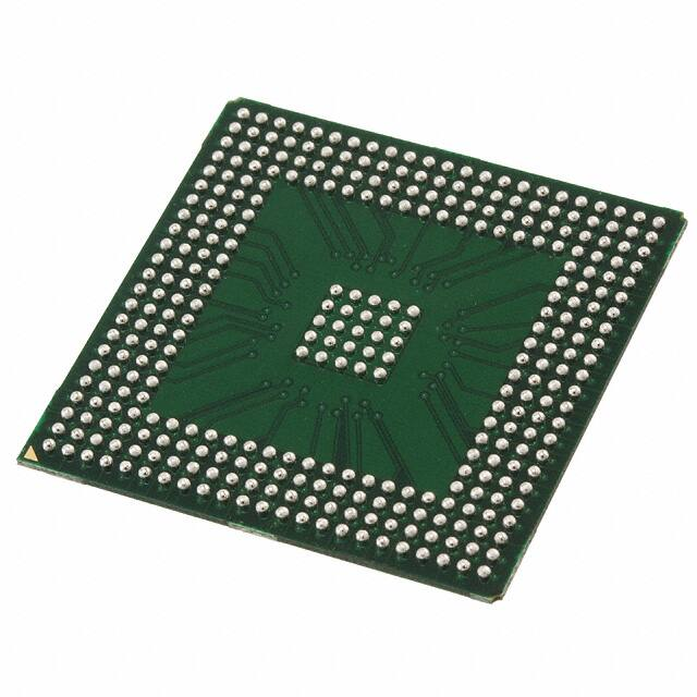


 工商网监
湘ICP备2023018690号
工商网监
湘ICP备2023018690号