AN1368
Developing Embedded Graphics Applications using PIC®
Microcontrollers with Integrated Graphics Controller
Author:
Pradeep Budagutta
Microchip Technology Inc.
FIGURE 1:
RED + GREEN = YELLOW
INTRODUCTION
Graphic-enabled devices are used extensively in daily
life. They are found everywhere, including indoor
products, such as telephones, calculators, pagers, MP3
players, digital electric meters, smart remote and UPS
displays. They are also used in outdoor products, such
as traffic signals, taxi meters, bus displays, advertisement boards, etc. The list is virtually endless. A current
trend is that many existing devices are becoming
graphic-enabled because it is economically feasible,
easy to use and the latest in technology.
This application note is intended to help engineers who
are designing their first graphic application. It describes
the basic definitions and jargons of graphics applications
and it helps the engineer to understand the theory,
necessary decision factors, hardware considerations,
available microcontrollers and development tools. Software libraries and support are available from Microchip
with further literature references for advanced users.
BASICS OF COLOR SCIENCE
In its purest form, color is associated with the
wavelength of light, within human visible range, from
about 400 nm (Violet) to 700 nm (Red), with Yellow
centered at about 575 nm. That means, if a light of
575 nm wavelength is incident on human eyes, it is
perceived as a Yellow light. We have also learned that
colors can be derived from three basic colors: Red,
Blue and Green. For example, Yellow can be derived
by mixing Red and Green lights. Is this true? The
answer is both no and yes. It is no because mixing Red
and Green lights will constitute a mixture of lights with
wavelengths of 700 nm and 560 nm, and there is not a
wavelength representing Yellow. The answer is yes
because human eyes perceive this mixture as a Yellow
colored light. Therefore, we see the mixture of Red and
Green lights as a single Yellow light, as shown in
Figure 1. This is due to the color recognition properties
of the human eye.
2011 Microchip Technology Inc.
Human eyes perceive the light as a Yellow colored light
instead of separate Red and Green colored lights. This
color recognition property of the human eye is the
foundation of the RGB (Red, Green and Blue) model.
The model states that the human eye can be made to
perceive different colors by mixing appropriate
proportions (intensities) of Red, Blue and Green colors.
Therefore, a ‘colored’ light can be formed by mixing
different proportions of Red, Green and Blue colors.
• Mixing the same proportions of three RGB colors
gives a Gray color
• Mixing a zero amount of all RGB colors gives a
Black color
• Mixing a maximum amount of all RGB colors
gives a White color
Varying the intensity of light, while keeping the same
proportion of RGB, gives different shades of Gray,
which is also known as ‘Grayscale’. Using a single
color (a fixed proportion of RGB) throughout an application gives a ‘Monochrome’ application, meaning a
single color.
Since everything is represented in bits and bytes in a
digital system, then how can actual colors be represented as a number in the form of bits or bytes? Each
of these three basic colors (RGB) can represent a byte
for a number ranging from 0 to 255. Therefore, with
3 bytes, we can represent 16 million colors (224) and
this is termed as “True Color”. It is also common to use
16 bits to represent colors. With 16 bits, we can
represent 64K colors (216), which is sufficient for many
graphics applications.
DS01368A-page 1
�AN1368
In general, to divide 16 bits among Red, Green and
Blue, two schemes are used:
FIGURE 3:
GRAYSCALE VALUES OF
0 TO 225
• Scheme 1 (R G B): In this scheme,
there are 5 bits of Red, followed by 6 bits of Green
and 5 bits of Blue. Green is given more bits
because of the property of the human eye, which
can distinguish more shades of Green than Red
and Blue. Figure 2 illustrates these 64K colors.
• Scheme 2 (T R G B): In this
scheme, there is one transparent bit, followed by
5 bits each of Red, Green and Blue. The
transparent bit indicates if the color should be
used or not.
Currently, the Microchip Graphics Library (Version 2.11)
supports only Scheme 1.
FIGURE 2:
COLORS IN 16-BIT
REPRESENTATION
Alternatively, color may be represented using a Color
Look-up Table (CLUT), also called a palette table, where
the color is specified by the index of the table, as shown
in Figure 4. Depending on the size of the table, the bits
used to represent the index will vary as 256 entries of
RGB (8-bit index), 16 entries of RGB (4-bit index),
4 entries of RGB (2-bit index) and 2 entries of RGB (1-bit
index). This scheme is mainly used to save memory. For
more information on this scheme, see Appendix A:
“Color Look-up Table (CLUT)”.
FIGURE 4:
COLOR LOOK-UP TABLE
(CLUT)
Grayscale is usually represented in a byte, with 0 as
Black, 1-254 as the shades of Black, getting lighter as
the number increases, and 255 as White, as shown in
Figure 3. Sometimes, only 4 or 2 bits are used to
represent 16 or 4 shades of Black, respectively. If only
one bit is used to represent either the on or off of a
color, then it is called ‘Monochrome’.
The number of bits required to represent a color is
called the ‘Color Depth’. For example, a color depth of
16 bits means it requires 16 bits to represent a color,
and therefore, we can represent 216 different colors.
DS01368A-page 2
2011 Microchip Technology Inc.
�AN1368
BASIC DISPLAY TERMINOLOGY
A screen is made up of discrete elements, known as
pixels. Every pixel can show one point of color and
each pixel is composed of three points: Red, Green
and Blue. The colors are arranged next to each other
on a color screen, one point of intensity on a grayscale
screen or one point that can be set to on/off on a
monochrome screen. The number of such pixels in
horizontal and vertical directions is called the screen
resolution. For example, a resolution of 320x240
means there are 320 pixels horizontally (number of
columns) and 240 pixels vertically (number of rows).
Standard resolutions are given names, such as QCIF
(176x144), CIF (352x288),QVGA (320x240), WQVGA
(480x272), VGA (640x480) and WVGA (800x480), etc.
While mentioning the resolution, it is always better to
refer to the numbers instead of the names.
FIGURE 5:
A screen can be in Landscape mode (width > height) or
in Portrait mode (height > width). The ratio of the
display screen’s visible width to its visible height is
called the ‘Aspect Ratio’. The most commonly used
aspect ratio is 4:3. The diagonal length of the display
screen is termed as the length of the display.
For example, a display of 3.5'' means that the diagonal
length of the display is 3.5'', as shown in Figure 5.
A 3.5'' QVGA DISPLAY IN LANDSCAPE MODE
320 Pixels
3.5''
240 Pixels
2011 Microchip Technology Inc.
DS01368A-page 3
�AN1368
GRAPHICS SUBSYSTEM HARDWARE
COMPONENTS OF A GRAPHICS
SYSTEM
The hardware components required for a graphic application, with their interconnection and design decisions,
are described in the following subsections.
FIGURE 6:
There are four basic components for any embedded
graphics system, as illustrated in Figure 6. They
consist of the display glass, display controller, frame
buffer and the microcontroller.
THE FOUR BASIC COMPONENTS OF A GRAPHICS SYSTEM
Frame
Buffer
Display
Controller
Display Glass
Microcontroller
Display Glass
Display glass is the device which displays a sequence of
colors on the pixels and also converts the digital
representation of colors to actual colors. The term, color,
includes grayscale. Generally, the types of displays used
are TFT LCDs, CSTN/MSTN LCDs or OLED/AMOLEDs.
All the LCD modules include gate and source drivers to
drive the voltage and current for displaying all the
pixels. Table 1 gives a brief comparison of different
display technologies.
COMPARISON OF DIFFERENT DISPLAY TECHNOLOGIES (1)
TABLE 1:
Property
TFT LCD
STN (CSTN/MSTN)
AMOLED
High
Low
High
Ghosting
No
Yes
No
HBLANK and VBLANK
Yes
No
Yes
Backlight
Required
Required
Not Required
Cost
Medium
Low
High
1.5" to 5.7"
1.5" to 5.7"
Up to 2.8"
Medium
Low
High
High
Medium
Low
Medium
Medium
High
Frame Rate
Typical Size for QVGA
(320x240) Resolution
Contrast
Power Consumption
Viewing Angle
Note 1:
Data mentioned in this table may change due to constant changes or advancements in the display
technology.
DS01368A-page 4
2011 Microchip Technology Inc.
�AN1368
Some of the important properties
technologies are explained as follows:
of
display
• Frame Rate: The number of times the display
screen is refreshed in a second (this parameter
does not reflect the refresh capacity of the
microcontroller but only the capacity of the display
glass).
• Ghosting: When the screen is changed, the
previous frame is visible with lower intensity for a
fraction of time, which appears to be the ghost of
the current screen.
• HBLANK and VBLANK: Horizontal and vertical
blanking periods, where the display is not updated.
For more information, refer to Section 43. “Graphics Controller Module (GFX)” (DS39731) in the
“PIC24F Family Reference Manual”.
• Backlight: For TFT/STN LCDs, backlight is
necessary to view the display. It could be either
CCFL or LED type.
• Contrast: It is defined as the ratio of intensities of
white to black on the display. The higher the
contrast, the better is the display quality.
• Viewing Angle: It is the horizontal or vertical
angle within which the display is properly
viewable.
The display glass has no inherent memory and must be
constantly updated with pixel data in each row and
column, failing which, the display will go blank (similar
to DRAM refresh). This refreshing of the display data is
handled by the display controller.
Frame Buffer
The frame buffer is a memory (usually a RAM), which
holds the data to be shown on the display screen and
acts as the data source for the display controller. The
required size of the frame buffer depends on the
resolution and color depth. The minimum requirement
is that it should hold the data required to display one full
frame and must support the scan rate (preferred
refresh rate as per the data sheet of the display glass)
of the display controller.
EQUATION 1:
Frame Buffer Size Required (Bytes) = Number of Pixels x
Color Depth (Bits)/8
EXAMPLE 1:
For a QVGA (320x240) display using a 16 BPP color
depth:
Frame Buffer = 320 x 240 x 16/8
= 153,600 Bytes
= 150 Kbytes
EXAMPLE 2:
For a WQVGA (480x272) display using a 16 BPP
color depth:
Frame Buffer = 480 x 272 x 16/8
= 261,120 Bytes
Display Controller
The display glass must be constantly refreshed by
feeding the horizontal and vertical pixel data repeatedly
from the frame buffer. This task is performed by the
display controller. It fetches the data from the frame
buffer, decodes it to the required bit format and feeds it
to the display glass, along with proper control signals.
The display controller must adhere to the timing
requirements of the display glass.
= 255 Kbytes
EXAMPLE 3:
For a QCIF (176x144) display using an 8 BPP color
depth:
Frame Buffer = 176 x 144 x 8/8
= 25,344 Bytes
= 24.75 Kbytes
2011 Microchip Technology Inc.
DS01368A-page 5
�AN1368
Microcontroller
The application code running inside the microcontroller
decides which data should be stored in the frame
buffer, and as the frame buffer changes, the display
content also changes. Each pixel’s color is calculated
and stored in the frame buffer. The microcontroller and
the display controller must have the same settings, with
respect to the color depth and memory range of the
frame buffer being used. The microcontroller must
have sufficient processing power (usually measured in
MIPS) to render the required shapes in the frame
buffer, such that it does not appear to be drawn slowly
on the display screen. This is because the display
FIGURE 7:
controller keeps pumping data from the frame buffer
concurrently, with the microcontroller rendering pixels
into the frame buffer. However, the microcontroller
does not render any new shapes into the frame buffer
if there is no change on the display screen. If there is a
change on the screen, only the changed pixels need to
be sent to the frame buffer, thereby minimizing the data
transfer to the frame buffer.
In Figure 7, only four pixels will be changed, and at a
16-bit color depth, 4 * 16/8 = 8 bytes need to be sent
to the frame buffer.
PIXEL DATA UPDATE
Display Glass
Frame
Buffer
Display
Controller
Microcontroller
DS01368A-page 6
2011 Microchip Technology Inc.
�AN1368
INTEGRATION OF BASIC
COMPONENTS
The choice of how to integrate the four basic
components is an important step in designing a
graphics application. To make the choice, the designer
FIGURE 8:
needs to understand the types of combinations of these
basic components that are possible in the form of ICs.
There are four types of possible combinations, as
illustrated in Figure 8.
Table 2 lists the advantages and disadvantages of the
four combinations of the basic components.
DIFFERENT WAYS OF INTEGRATING BASIC GRAPHICS’ COMPONENTS
Display Module
Parallel or
Serial
Frame
Buffer
Display
Controller
Display Glass
A. 2 Devices
Microcontroller
Graphic Controller Chip
Parallel or
Serial
B. 3 Devices
Frame
Buffer
Display
Controller
RGB
Display Glass
Microcontroller
Frame
Buffer
Display
Controller
RGB
Display Glass
RGB
Display Glass
Microcontroller
C. 2 Devices
SRAM
Frame
Buffer
D. 3 Devices
Display
Controller
Buffer
Parallel
Microcontroller
2011 Microchip Technology Inc.
DS01368A-page 7
�AN1368
TABLE 2:
BASIC COMPONENTS
Options
Advantages
Disadvantages
A. The frame buffer and display
controller are housed in a single
module, called the ‘Display Module’.
The microcontroller and display
module interface through a serial or
parallel interface.(1)
• No specific IC is required for graphics
functionality
• Less system components and less PCB
space
• Generally higher cost
• Usually forces a
software driver change
if the display module is
changed
• May lack additional
memory required for
double-buffering,
animation, etc.
B. The frame buffer is housed
together with the display controller.
The microcontroller and graphics
controller communicate through a
serial or parallel interface, whereas
the graphics controller interfaces to
the display glass through an RGB
interface.(1)
• Software driver change is not required if
the display glass is changed. Only a
compile-time configuration change may be
needed.
• Can be cheaper than Option A
• More system components and more PCB
space
• Display size is limited
by the frame buffer
inside the display
controller
C. The frame buffer and display
controller are housed inside the
microcontroller. The microcontroller
interfaces to the display glass
through an RGB interface.
Instead of a display controller, a
combination of a parallel interface
and a DMA engine can be used as
well.
• Only one IC is required for graphics
functionality
• Small form factor
• Usually the cheapest option
• Faster rendering since the memory is inside
the microcontroller
• Software driver change is not required if the
display module is changed. Only a
compile-time configuration change may be
needed.
• Display size is limited
by the frame buffer
inside the
microcontroller
D. The display controller is housed
• The microcontroller can support the
inside the microcontroller. Separate
maximum display size possible as the size
RAM is used as the frame buffer.
of the frame buffer can be selected by the
The microcontroller interfaces to the
user
display glass (display panel) through • Usually cheaper than Option A and B
an RGB interface and interfaces with
the frame buffer through a parallel
interface.
Instead of a display controller, a
combination of a parallel interface
and a DMA engine can be used as
well.
Note 1:
• Requires an extra IC
chip for the frame
buffer
A serial connection can be used on low resolution displays with low color depth (e.g., 1 BPP, 120x64). With
higher resolutions, the speed can be a bottleneck.
For Options A and B, the Microchip Graphics Library
currently supports PIC24, dsPIC® and PIC32
microcontrollers with PMP or EPMP. The
PIC24FJXXXDAXXX family can support Options C and
D. PIC24FJ256DA210 contains 96 Kbytes of internal
memory and has a graphics controller inside. It also
DS01368A-page 8
supports optional external RAM as a frame buffer with
a parallel interface through the EPMP module. For
more information on the device, refer to the respective
device data sheet and also Section 43. “Graphics
Controller Module (GFX)” (DS39731) from the
“PIC24F Family Reference Manual”.
2011 Microchip Technology Inc.
�AN1368
Depending on the design of the display panel, all four
types of the power signals can be found in the panel
data sheet. In some cases, only the digital power and
backlight signals appear. This means that the panel
has integrated an internal circuitry to generate the
analog and LCD power signals. This is usually true for
small displays (2'' to 4''). For larger displays, the analog
and LCD power signals tend to be higher in voltage
requirements. In these cases, it is not practical for the
display panel to integrate such circuitry; therefore,
those two power signals, that are specified as inputs,
must be externally provided.
POWER SEQUENCING IN DISPLAY
PANELS
Different display panels will have different power supply
requirements and timing to enable each of the power
signals of the panel. In some display panels, the
following power signals can be found:
•
•
•
•
Digital Power Signal
Analog Power Signal
LCD Power Signal
Backlight Power Signal
The digital power signal is used to power-up the digital
logic on the panel. The analog power signal is used to
power the analog portion of the panel. The LCD power
signal, also known as the gate voltage, along with the
digital data signals are primarily used to control the
pixel illumination. In some cases, the LCD power signal
is composed of two power signals: the positive LCD
power signal and the negative LCD power signal. In
some cases, only one signal is available. The backlight
illumination is controlled by the backlight power signal.
FIGURE 9:
The different power signals of the display panel must
follow the power sequencing recommended by the
manufacturer. If the proper sequence is not followed,
the display panel’s life cycle can be reduced
significantly. The typical power sequence of a panel is
shown in Figure 9.
Timing requirements are represented by t1, t2, t3, t4, t5
and t6. In most cases, the requirements are
represented as t1 = t4, t2 = t3 and t5 = t6.
POWER SEQUENCE OF A PANEL
Voltage
t1
t2
t3
t4
VLCD
VA
VD
Time
t5
VBK
t6
Data
Time
VD = Digital Supply
VA = Analog Supply
VBK = Backlight Supply
VLCD = LCD Supply
Data = Digital Signal from Controller
2011 Microchip Technology Inc.
DS01368A-page 9
�AN1368
TOUCH SCREEN
4-WIRE RESISTIVE TOUCH SCREEN
Some applications require the support of a touch
screen for the display. This is achieved by using a
separate touch screen on the display glass or by
selecting a display module with a touch screen. In both
cases, the touch signals must be handled by either the
microcontroller or a separate touch screen controller
(such as Microchip’s AR1000 series touch screen
controllers). These touch signals are analog and digital
signals which must be decoded to sense the touch
coordinates. Transparent touch screens are usually of
resistive type or capacitive type. Resistive touch
screens are the most commonly used and are
generally available in 4-wire or 5-wire configurations.
The touch point can be detected by measuring the
variation of the resistance of the touch screen. Only a
4-wire touch screen is explained here.
This touch screen has four signals, of which two are
purely digital signals. The other two signals are
alternately configured as both digital and analog signals.
FIGURE 10:
The four signals can be directly connected to the
microcontroller I/O pins with two digital inputs and two
digital outputs, or analog pins. Figure 10 illustrates the
connections for this scheme.
When the user touches the screen, the resistance of
the screen changes. By measuring the resistance in
horizontal and vertical directions, and comparing them
with the calibrated values, the (x, y) coordinates of the
point of touch can be obtained.
When a point on the screen is touched, the x-coordinate
voltage is obtained by applying voltages across the ysignal and measuring the analog voltage on the x-signal,
as shown in Figure 11. The y-coordinate voltage is
obtained by applying voltage across x-signals and
measuring the analog y-voltage, as shown in Figure 12.
4-WIRE RESISTIVE TOUCH SCREEN
Y
PIC® MCU
with ADC
Digital I/O
Digital I/O
X
X
Digital I/O
Digital I/O
Y
DS01368A-page 10
2011 Microchip Technology Inc.
�AN1368
FIGURE 11:
MEASUREMENT OF THE X-VOLTAGE
Y
PIC®MCU
with ADC
Digital I/O
1
Digital I/O
Dig-O/AN-I
Dig-O/AN-I
X
Sense
X
0
Y
FIGURE 12:
MEASUREMENT OF THE Y-VOLTAGE
Y
PIC ® MCU
with ADC
Digital I/O
1
Digital I/O
Dig-O/AN-I
Dig-O/AN-I
0
X
X
Sense
Y
DECISION FACTORS
Display Resolution and Size
After understanding the basic definitions and
components of a graphics subsystem, the next step is
to decide the specifications for the application. Some of
the important factors that needs to be considered when
deciding on specifications are as follows:
A particular resolution can be obtained in different
display sizes. For example, QVGA (320x240) displays
are available in a size range of 1.5'' to 5.7''. As the size
increases, keeping the resolution constant, the pixels
will look coarser, that is, curved shapes on the screen
will appear blocky.
•
•
•
•
•
•
•
•
Display Resolution and Size
Display Orientation – Portrait or Landscape
Color Depth (BPP)
Frame Buffer Size
Microcontroller Processing Power
Configuration of Graphics Components
Frame Rate vs. MIPS
Interfacing with Unmatched Number of Display
RGB Lines
These decision factors are described in the following
sections.
In an application, if the user needs to look at the display
from a short distance (e.g., hand held devices), higher
resolution displays are a better choice for larger
displays. If the user looks at the display from a long distance (e.g., token number of displays at banks), larger
sized displays with lower resolution may be used. If
pictures are being displayed, it is better to use a higher
resolution. Figure 13 illustrates how ‘A’ appears on a
smaller sized lower resolution display, larger sized lower
resolution display and larger sized higher resolution
display, respectively.
FIGURE 13:
2011 Microchip Technology Inc.
DISPLAY OF ‘A’ AT
VARIOUS RESOLUTIONS
DS01368A-page 11
�AN1368
Display Orientation
Color Depth Selection
Displays are available in Landscape (e.g., 320x240) or
Portrait (e.g., 240x320) modes. A landscape display
can also be used in Portrait mode by setting a 90°
rotate function in the graphics library or display
controller. Similarly, a portrait display can also be used
in Landscape mode. If rotating the pixels is
implemented by special hardware features inside the
graphics controller, there is no penalty on the
performance. However, if the rotation is performed in
software (such as the graphics library used), there is a
penalty in the software performance. This is because
for every (x, y) point, a new rotated (x’, y’) point has to
be calculated, which takes away some of the
processing power.
Along with the resolution of the display, the correct
choice of color depth is another decision factor since
this determines the size of the frame buffer (cost of
RAM). If natural photos are being displayed, it is better
to go with 16 BPP or higher. If 256 different colors are
enough for the application, then a color depth of 8 BPP
can be chosen (with the standard 256 colors provided
by the display controller or custom 256 colors using
CLUT (See Appendix A: “Color Look-up Table
(CLUT)”). This would reduce the RAM requirement by
50%, compared to 16 BPP. If only 16 or 4 different
colors are sufficient, 4 BPP or 2 BPP can be used,
saving the RAM by 75% and 87.5%, respectively, as
compared to 16 BPP. Table 3 lists the RAM
requirements for different color depths.
Note the difference in the RGB strip alignment if the
display is used in Rotated mode, as shown in
Figure 14.
FIGURE 14:
TABLE 3:
LANDSCAPE AND PORTRAIT DISPLAYS USED IN LANDSCAPE MODE
RAM SIZE REQUIREMENT FOR DIFFERENT COLOR DEPTHS
BPP for QVGA (320x240)
16 BPP
8 BPP
4 BPP
2 BPP
Number of Colors
65,536
256
16
4
RAM Size (Bytes)
153,600
76,800
38,400
19,200
DS01368A-page 12
2011 Microchip Technology Inc.
�AN1368
Frame Buffer Size
Configuration of Graphics Components
The size of the frame buffer is calculated as follows:
In Table 2, each configuration has its own advantages
and disadvantages.
EQUATION 2:
Frame Buffer (Bytes) = Total_number_of_pixels x
Color_Depth (in BPP)/8
Table 3 shows an example for the QVGA (320x240)
display. If the double-buffering technique is used, the
frame buffer requirement will double (see Appendix B:
“Double-Buffering” for more information).
If the frame buffer is inside the display controller or the
smart display module, and if the RAM is fixed, the
maximum resolution that can be supported is limited.
Processing Power (MIPS)
The processing power required is application-specific.
It depends on how many graphic elements are
displayed on the screen and the complexity of the
graphic elements. More processing power is required
to draw complex shapes, such as a circle, bevel, text,
etc., rather than lines and rectangles. The processing
power requirements also depend on if a hardware
graphics accelerator is available and used. Processing
power requirements also depend on the update rate of
the screen elements. For many embedded graphics
applications, ≥ 16 MIPS processing power could be
sufficient. The best way to check the processing power
requirements is to evaluate using the standard
graphics development tools. (For more information on
development tools, see the “Development Tools”
section.
2011 Microchip Technology Inc.
Most often, the decision to use one or another
configuration is not influenced by the technical advantages or disadvantages, but rather by a supply chain
advantage or the availability of components. The
designer must balance between optimizing a design to
meet the requirement and managing the supply chain.
Frame Rate VS. MIPS
Frame rate refers to the number of different frames that
can be displayed in a second. This is a good
performance index for display of a video, but not for an
embedded GUI application. In general, an embedded
application does not always change the entire screen,
instead it changes a part of the screen, like a button or
a check box. The amount of change depends on the
size of the changed widget. The update time also
depends on factors, such as if the change belongs to a
widget or an image. It is important to consider the
worst-case scenario on the planned application. Initial
calculation of frame rate and MIPS is important to get
the preliminary requirements for the system. In addition
to these calculations, it is recommended to evaluate
the system using development tools, such as
evaluation kits.
DS01368A-page 13
�AN1368
Interfacing with an Unmatched Number
of Display RGB Lines
It is possible that the display controller’s number of
RGB line outputs is different from the number of RGB
line inputs of the display; it is still possible to interface
both of them. If the display’s RGB input lines are equal
to the display controller’s RGB line outputs, there will
be no color degradation. If not, there may be a slight
color degradation because the display panel will be
unable to display all the colors generated by the display
controller. Usually, the former case is encountered
rather than the latter.
FIGURE 15:
In Figure 15, the display panel has more RGB signal
lines than the display controller. Here, all the RGB lines
of each color of the display controller are connected to
the MSbs of the display’s display signal lines. The
unconnected LSbs may be connected to Ground or
VDD, or to the MSb of the same color. Connecting the
LSbs to the MSbs is the widely used method, since this
enables the display to have a wider range of color
values.
DISPLAY CONTROLLER’S DISPLAY SIGNALS LESS THAN LCD’S DISPLAY
SIGNALS
RGB 666 (Display)
RGB 565
Red [4]
dp_Red [5]
Red [0]
dp_Red [1]
Connect to VDD or GND or MSb
dp_Red [0]
dp _Green [5..0]
Green [5..0]
Blue [4..0]
dp_Blue [5..1]
dp_Blue[5]
Connect to VDD or
GND or MSb
DS01368A-page 14
or
dp_Blue[0]
2011 Microchip Technology Inc.
�AN1368
In Figure 16, the display LCD has less display signal
lines than the display controller.
FIGURE 16:
The MSbs of the display lines of each color of the display controller are connected to all the display signal
lines of the LCD. The unconnected LSbs may be left
unconnected.
DISPLAY CONTROLLER’S DISPLAY SIGNALS ARE MORE THAN LCD’S DISPLAY
SIGNALS (POSSIBLE COLOR DEGRADATION)
RGB 585 (Display)
RGB 666
dp_Red [4]
Red [5]
dp_Red [0]
Red [0]
No Connect
dp _Green [5..0]
Green [5..0]
Blue [4..0]
Blue [0]
2011 Microchip Technology Inc.
dp_Blue[4..0]
No Connect
DS01368A-page 15
�AN1368
THE PIC24FJ256DA210
MICROCONTROLLER
The PIC24FJ256DA210 device is a 16-bit microcontroller which supports a processing speed of up to
16 MIPS. The microcontroller includes 96 Kbytes of
internal RAM and a built-in display controller with
Graphics Processing Units (GPUs) to accelerate the
drawing of common 2D shapes.
PIC24FJ256DA210 GRAPHICS CONTROLLER MODULE
PIC24F Graphics
Controller Module
Display Interface
Clock (DISPCLK)
System Clock
Display Module
Interface
Registers
and Control
Interface
GD
HSYNC
Graphics
Controller Clock
(G1CLK)
GPU Command
Interface
RCCGPU
CHRGPU
VSYNC
GEN
IPU
CLUT
Memory Request Arbiter
To Display
Glass
FIGURE 17:
It can also interface with optional, external parallel
RAM through the Enhanced PMP module to increase
the size of the frame buffer. The PIC24FJ256DA210
graphics controller module is shown in Figure 17.
GPWR
GCLK
System
RAM
DS01368A-page 16
2011 Microchip Technology Inc.
�AN1368
• DISPCLK is the clock which drives the display
glass.
• System clock is the clock speed at which the
program accesses the Command/Control/Status
registers.
• G1CLK is the clock which drives the GPUs to
draw lines, rectangles, render characters and
decode compressed data without the involvement
of the processor.
• External RAM, up to 16 MB, can be connected
through the EPMP module using a parallel interface. The graphics module can use this on its own
without any involvement of the processor. The
interfaces allowed are limited to an 8-bit or 16-bit
parallel connection. For more options and information, refer to Section 42. “Enhanced Parallel
Master Port (EPMP)” (DS39730) in the “PIC24F
Family Reference Manual”.
• HSYNC, VSYNC are the horizontal and vertical
synchronization signals to the display.
• GCLK is the pixel clock.
• GEN is a signal that varies in function for TFT and
STN display types of interfaces. For TFT, this signal indicates that data lines are valid. For STN,
this signal toggles per line on the Line Toggle
mode and toggles per frame for the Frame Toggle
mode. For more information, refer to Section 43.
“Graphics Controller Module (GFX)”
(DS39731) in the “PIC24F Family Reference
Manual”.
• GD carry the display RGB or Gray values
as per the graphics module settings. Only the
required number of lines is enabled, depending
on the interface requirements of the display. (e.g.,
16 lined for TFT LCD’s RGB565 input or four lines
for MSTN’s grayscale input).
TABLE 4:
• GPWR is the power supply control signal for the
display glass. In some large displays, an external
circuitry may be needed. Use this signal to enable
or disable the external power circuitry. In displays
that include an internal power circuitry, this signal
can be connected to the display’s power enable
pin. This signal should not be used as a power
supply line to the display glass.
Table 4 lists the number of microcontroller pins
required for various display and RAM configurations.
The Graphics Processing Units (GPUs) like the
Character Graphical Processing Unit (CHRGPU),
Rectangle Copy Graphics Processing Unit (RCCGPU)
and Inflate Processing Unit (IPU) are the graphics
accelerators. These accelerators are used for
rendering characters, rectangles and to decompress
the compressed data, respectively.
These GPUs help to free the processing power of the
microcontroller, which can be used for the purpose of
the application. Instead of the CPU rendering the
pixels, the application only needs to issue the
commands to draw primitive rendering functions (such
as lines, bars and characters) to the screen. After
issuing the commands, the CPU is free to perform
other application tasks. The application code runs in
parallel to the RCCGPU, which concurrently draws the
line. However, care should be taken because returning
from a function, for example, Line(), need not imply
that the line is completely drawn. This is called a nonblocking draw. The drawing can also be made blocking
by setting the proper compiler switch in the
GraphicsConfig.h file, as explained in future
sections.
MICROCONTROLLER PINS
Configuration
A TFT LCD without External RAM (using CLUT
and 16-bit colors)
Display Data
Pins (RGB)
EPMP
Pins
Other (Clock
and Sync)
Pins
Total
16
0
5
21
A 256-Color CSTN without External RAM
8
0
5
13
A TFT LCD with External 16-Bit Wide RAM of
256 Kbytes (using 16-bit colors)
16
37
5
58
A 16-Color MSTN without External RAM
4
0
5
9
2011 Microchip Technology Inc.
DS01368A-page 17
�AN1368
The GPUs are briefly explained below:
• CHRGPU: Renders the characters on the display.
A font table must be loaded into the RAM and the
CHRGPU must point to that font table. The (x, y)
coordinates must also be initialized on the appropriate CHRGPU registers. When a character code
and the draw command are given, the character
will be rendered on the configured RAM area,
which can also be the frame buffer. The user must
take care of the display glass orientation as the
characters cannot be rotated dynamically by the
CHRGPU. The CHRGPU does not support antialiased fonts; all the pixels on a character are of the
same color. The background and foreground colors
are set using the CHRGPU commands. If transparency is enabled, only the foreground color is
drawn, and if the transparency is disabled, the
background color is also drawn surrounding the
character. To use the CHRGPU by default, uncomment the line: #define USE_DRV_OUTCHAR in
MicrochipGraphicsModule.h.
• RCCGPU: Used to draw horizontal or vertical
lines, rectangles, filled rectangles, and to copy
rectangular regions. RCCGPU can perform the
following three operations:
- Copy – Copy a memory block from one part
of the RAM to another. Depending on the
command parameter, the block of memory
can be a contiguous block or a rectangular
block.
- Copy with Solid Fill – Fill a rectangular area
with a specific color.
- Copy with Transparency – Same as the copy
option, but a color set apart to indicate transparency will not be copied to the destination,
leaving that part of the destination
unchanged.
Each operation can use one of the 16 available logical
operations, called Raster Operations (ROPs), which is
applied while copying.
The RCCGPU can be used to achieve special effects,
such as screen animations, like scrolling, peeling, etc.
For more information on the advanced usage of the
RCCGPU, see Appendix C: “Advanced Usage of
RCCGPU”.
• IPU: Used to decompress a compressed data
using the DEFLATE algorithm with Fixed Huffman
codes. For example, images can be compressed
and kept in the internal Flash or external memory
and they can be decompressed into RAM during
run time. Similarly, compressed user-specific data
can also be decompressed and used during run
time with the IPU. It should be noted that
decompression can only commence from the
beginning of a compressed block and not from the
middle. For example, when storing multiple
images, compress each image to its own
compressed block. The IPU can be used to
decompress any images by specifying the
location of the desired compressed block. The
Microchip Graphics Library will handle this
scenario, making it transparent to the users.
Note:
Bit maps can be compressed by selecting
the “IPU” option in the Graphics Resource
Converter (GRC) tool while converting the
images. GRC is a tool included in the
installation of the Graphics Library. The
PutImage() API automatically decompresses these compressed images using
the IPU at run time. The user is required to
allocate the required amount of RAM for
IPU operation, using compile-time options
as described in the Microchip Graphics
Library Help file.
For more information on these GPUs and their
registers, refer to Section 43. “Graphics Controller
Module (GFX)” (DS39731) in the “PIC24F Family
Reference Manual”.
For example, source can be copied as is or the source
can be ORed with the destination area, or the source
can be ANDed with a separate region and copied to the
destination area. For more information on the Graphics
Controller Module (GFX) and the supported ROPs,
refer to the Section 43. “Graphics Controller Module
(GFX)” (DS39731) in the “PIC24F Family Reference
Manual”.
DS01368A-page 18
2011 Microchip Technology Inc.
�AN1368
DEVELOPMENT TOOLS
A fast and cost-effective way of evaluating the system
specification of an application is through the use of
existing development tools. Microchip has several
development tools supporting graphics design. Two
important tools that can be used for graphics
development are:
• Graphics LCD Controller PICtail™ Plus SSD1926
Board (AC164127-5), which is an add-on board to
the Microchip’s generic development board for
16-bit and 32-bit microcontrollers, such as the
Explorer 16 board and PIC32 starter kits.
• PIC24FJ256DA210
Development
Board
(DM240312), which is a stand-alone board.
Both the boards require add-on display modules which
are available with displays of various sizes. Userspecific display panels can be used with the help of a
display prototype board. Figure 18, Figure 19, Figure 20
and Figure 21 illustrate these development tools. For the
latest tool set, visit: http://www.microchip.com/graphics.
FIGURE 18:
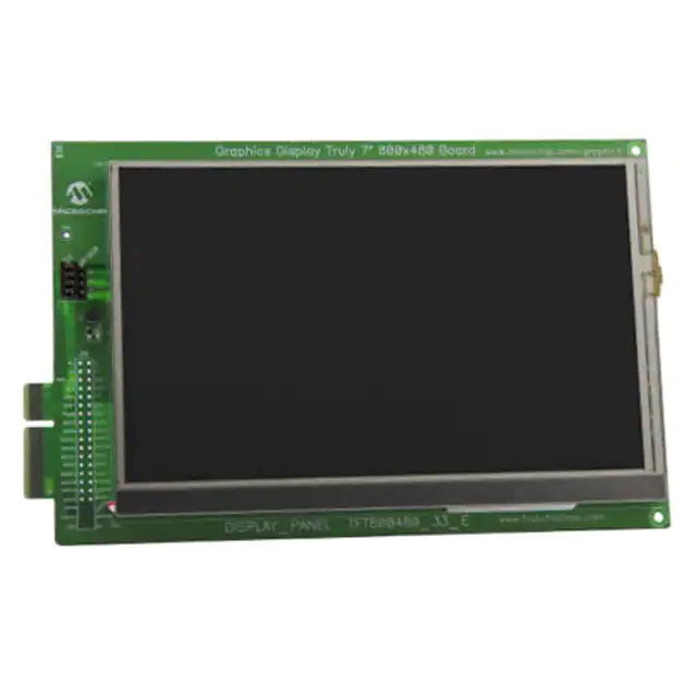
GRAPHICS PICtail™ PLUS DAUGHTER BOARD WITH 3.2'' DISPLAY KIT (AC164127-3)
FIGURE 19:
DEVELOPMENT BOARD SUPPLIED WITH PIC24FJ256DA210 DEVELOPMENT KIT
(DV164039)
2011 Microchip Technology Inc.
DS01368A-page 19
�AN1368
FIGURE 20:
4.3'' WQVGA POWERTIP TFT DISPLAY BOARD (AC164127-6)
FIGURE 21:
GRAPHICS DISPLAY PROTOTYPE BOARDS (AC164139)
DS01368A-page 20
2011 Microchip Technology Inc.
�AN1368
Features of the Microchip Graphics Library are:
SOFTWARE
The basic software component required for any
graphics application is a Software Display Driver which
provides one basic operation (i.e., setting the color of a
pixel). A driver may also implement APIs to draw
fundamental shapes, for instance, a line, rectangle,
bar, circle, text, image and so on. The Software Display
Driver must be written for every separate graphics
driver used. More complex graphic elements, like
labels, buttons, check boxes, sliders and progress bars
are implemented in higher layers, which in turn, use the
Software Display Driver.
Microchip provides a ‘free to use on PIC MCU’ software
library, called “Microchip Graphics Library”, which
contains the above discussed drivers and higher
layers. Several demos are distributed with the graphics
library which the user can run out of the box on the
appropriate development tools.
FIGURE 22:
• Works with 16-bit and 32-bit PIC® MCUs, as well
as dsPIC® DSCs
• Modular design, compile only what is required
• Supports multiple user interfaces
• Not dependent on display size or resolution
• Low-cost, full-featured development tools
• Utilities to import fonts and images
• Free to Microchip customers
• Includes multiple low-level drivers
The structure of the Microchip Graphics Library is
shown in Figure 22.
The Microchip Graphics Library v2.11 is distributed
along with the Microchip Applications Library and is
available for download at www.microchip.com/MAL.
STRUCTURE OF MICROCHIP GRAPHICS LIBRARY
Application Layer
User Message Interface
(Touch Screen, Keypad, and so on)
Graphic Object Layer
(Button, Slider, Edit Box, and so on)
Graphic Primitive Layer
(Line, Circle, Bar, and so on)
Display Device Driver Layer
(PutPixel, SetColor, and so on)
Graphic Display Controller/Display Panel
Note:
The Microchip Graphics Library Version 2.11 is explained here. In future, the software structure may be modified. Refer
to the Help file of your Microchip Graphics Library for the latest information.
The Graphics Display Controller is the hardware module
consisting of the frame buffer and Display Controller.
The remaining layers are the software layers. The
Microchip Graphics Library is organized in a set of
folders under the folder, ‘Microchip Solutions’. The ‘C’
files are in the folder, Microchip Solutions/Microchip/
Graphics, and the header files are in the folder,
Microchip Solutions/Microchip/Include/Graphics. The
2011 Microchip Technology Inc.
development board-specific files are in the folder,
Microchip Solutions/Board Support Package. The
project path must be set to point to these folders.
Starting from the bottom-most Software layer to the
top-most layer, the functionality of each layer and the
files responsible for those layers are explained further
in the following sections. For more information, refer to
the Help file of the Microchip Graphics Library.
DS01368A-page 21
�AN1368
DISPLAY DEVICE DRIVER LAYER
GRAPHIC PRIMITIVE LAYER
Every hardware display controller has its own set of
commands and status information. Therefore, separate
software drivers are needed for each supported display
controller, which fulfills the requirements of the display
driver and the standard APIs defined by the Graphics
Library. The list of supported drivers can be found in the
Graphics Library Help file. To know if a display module is
supported, check if the display driver inside the display
module is available in the above mentioned folder.
This is a layer above the Display Driver layer and
provides most common services through APIs, which
are used to draw basic shapes, for instance, line
(normal, thick, dashed), bar, rectangle, circle, polygon,
bevel and arc. It also provides APIs for drawing text
and images. These are generic APIs which work with
any given display driver. However, some of these APIs
may be implemented by the Driver layer for optimized
performance, especially if the driver supports 2DAccelerations (For example, the Microchip Graphics
module and SSD1926). It is possible to write simple
applications by using Primitive and Driver layers only
and without using higher layers. To include this layer,
the following files must be added to the project:
The main function provided by this layer is the
initialization of the driver using the API
ResetDevice(), painting a pixel using APIs,
SetColor(color) and PitPixel(x,
y), and
knowing the color of a pixel using the API
GetPixel(x, y). The other functionalities provided
are, for example, setting up of clipping area, getting the
maximum x and y values for a display screen, etc. An
application can be written using only this layer without
using any higher layers. In that case, all the shapes
must be drawn by the user. To include this layer, the
following files must be added to the project:
HEADER FILES
Graphics.h
DisplayDriver.h or specific
(like SSD1926.h)
CONFIGURATION FILES
HardwareProfile.h
GraphicsConfig.h
These files are project-specific and must be inside the
project folder.
SOURCE FILES
Specific (like SSD1926.c)
HEADER FILES
Primitive.h
SOURCE FILES
Primitive.c
GRAPHIC OBJECT LAYER (GOL)
The GOL consists of many selectable objects, called
‘widgets’, such as Button, TextBox, Check Box,
ScrollBar, ProgressBar, Picture, ListBox, GroupBox,
Meter, DigitalMeter, Dial, Chart and Grid, which form
the basic elements of a complex graphics application.
Each of these widgets is implemented in ‘C’, but with
basic object-oriented principles, and can be used as
modules. Use of this layer must be enabled at compile
time in the ‘GraphicsConfig.h’ file. The use of
individual widgets can be enabled or disabled during
compile time in the ‘GraphicsConfig.h’ file, thereby
saving RAM and ROM. For more information, see the
“Configuration” section.
Each kind of widget has a default style scheme which
defines the font and the colors used for various parts
and states of the widget. For example, a button in a
pressed state has a different color than the released
button. The style scheme for each widget is explained
in detail in the Help file of the Microchip Graphics
Library. For each style scheme, some heap memory
(dynamically allocated memory) is required to store the
style scheme values. Heap is required to store the state
information for each enabled widget. The total heap
must be greater than the sum of heaps for all the
instances of used widgets. Aside from the heap
requirement, each widget type also needs to use RAM
space for variables when rendering and managing the
widgets. This additional RAM requirement is a constant
overhead for each type of widget. The difference
between the two is that the heap requirement is needed
for each instance of a widget, while the RAM
requirement is needed for each type of widget. The
RAM requirement is constant and not dependent on the
number of instances of one type of widget.
DS01368A-page 22
2011 Microchip Technology Inc.
�AN1368
For example, if the Release note says:
Module
Button
GOL
Heap for PIC24F
28
(per instance)
20 (per style
scheme)
Heap for PIC32
44
(per instance)
24 (per style
scheme)
RAM for PIC24F
8
32
RAM for PIC32
12
28
ROM for PIC24F
1002
2076
ROM for PIC32
2748
5400
Note:
Users can also create their own widgets and add to the
graphics library. See “References” for more details.
File Category
Header Files
•
•
•
•
•
•
•
•
•
•
•
•
•
•
•
•
•
•
•
Configuration
Files
• GraphicsConfig.h (to
select the usage of GOL and
its individual widgets)
Source files
•
•
•
•
•
•
•
•
•
•
•
•
•
•
•
•
•
•
•
•
The RAM and ROM requirements for
PIC24F and PIC32 devices may be different because of different microcontroller
architecture and different compilers.
For a PIC24F application using only two buttons, a
RAM of 8 bytes, ROM of 1002 bytes and the required
heap memory would be 2 x 28 = 56 Bytes.
If one style scheme is used, then a heap memory of
20 bytes would be required.
EQUATION 3:
Total Heap (Minimum Required Heap) = 20
(for the Style Scheme) + (2 x 28) = 76 bytes
Total RAM (for Graphics) = 32 (for GOL) + 8 = 40 bytes
Note:
This example is indicative only. It is
recommended to see the release notes of
the Microchip Graphics Library to derive
the appropriate values for that particular
release.
The GOL depends on the Primitive and the Display Driver
layers. A function, GOLDraw(), must be called
continuously in a loop to simplify the drawing of widgets.
Additionally, a function, GOLDrawCallback(), must be
implemented in the application code. This is used for
custom drawing which is explained in the Help file.
Generally, this function can just return: TRUE.
To include the GOL, along with the files required for the
Primitive layer and Display Driver layer, the following
files must be added to the project. See the Help file for
the latest list of files. If the GOL is used, then in the
GraphicsConfig.h file, the macro, #define
USE_GOL, must be defined. Individual macros for the
widgets used, such as #define USE_BUTTON, must
also be defined. If these individual macros are not
defined, the widgets will not be compiled even if they
are included in the project.
Note:
2011 Microchip Technology Inc.
Button
GOL.h
Button.h
Chart.h
CheckBox.h
DigitalMeter.h
EditBox.h
Grid.h
GroupBox.h
ListBox.h
Meter.h
Picture.h
ProgressBar.h
RadioButton.h
RoundDial.h
Slider.h
StaticText.h
TextEntry.h
Window.h
GOL.c
GOLFontDefault.c
Button.c
Chart.c
CheckBox.c
DigitalMeter.c
EditBox.c
Grid.c
GroupBox.c
ListBox.c
Meter.c
Picture.c
ProgressBar.c
RadioButton.c
RoundDial.c
Slider.c
StaticText.c
TextEntry.c
Window.c
This list is for indication only. Refer to the
Microchip Graphics Library Help file for
the latest list of files.
DS01368A-page 23
�AN1368
USER MESSAGE INTERFACE
The user message interface is a sublayer of the GOL
which is enabled if the GOL is used. This sublayer is
used to facilitate the message passing between
widgets and user input. For example, if the user
presses a button, then a message is sent to a call back
function, called GOLMsgCallback(), where the
message indicating that the button is pressed is
checked and an action is taken. This callback function
must be present in the application code if the GOL is
being used, no matter if message passing is being
used or not. If the message passing is not used, the
function body must return a ‘1’.
Similar to GOLDraw(), GOLMsg() must be called
continuously in a loop inside the application code to
facilitate message collection and passing.
The usage of GOLDraw(), GOLDrawCallback(),
GOLMsg() and GOLMsgCallback() are explained in
Example 4, Example 5 and Example 6.
APPLICATION LAYER
In this layer, the user has full control of the application.
Initially, the user must initialize the Microchip Graphics
Library. The initialization is done by calling GOLInit() if
all the layers are being used, InitGraph() if the GOL
is not being used but the Primitive and Display Driver
layers are being used, or by calling ResetDevice() if
only the Display Driver layer is being used. After the
initialization routine, the Primitive and Driver layers’ APIs
can be called to achieve the required draw functionality.
To use GOL objects (like buttons), the widgets must be
created by calling the widget’s create function (e.g.,
BtnCreate()), one by one, until all of the widgets are
created. This step will not display the widgets. The
created widgets are drawn on the screen when the
GOLDraw() function is called repeatedly in a while loop.
The messages are processed by calling the GOLMsg()
inside the same loop, as shown in Example 5.
DS01368A-page 24
After GOLDraw() is done, messages are received
from the touch screen driver and hard buttons driver.
The obtained message is passed to GOLMsg() to
process and to output a widget-specific message. For
example, it converts a “USER TOUCHED POSITION
100, 100” message to BUTTON1_PRESSED.
Additionally, the application must possess the
GOLDrawCallback() and GOLMsgCallback()
functions.
If custom drawing is not done, then the draw callback is
used, as shown in Example 4.
EXAMPLE 4:
WORD GOLDrawCallback(void)
{
return (1);
}
The message callback handles the processed
message sent out by the widgets, as shown in
Example 6.
If the application already uses a main loop,
GOLDraw() and GOLMsg() can be called within the
loop (see Example 5).
Note 1: Refer to the application note, AN1136, “How
to Use Widgets in Microchip Graphics
Library” for creating a simple application.
2: Refer to the Microchip Graphics Library
Help file for the list of related application
notes.
2011 Microchip Technology Inc.
�AN1368
EXAMPLE 5:
while(1)
{
if(GOLDraw())
{
TouchGetMsg(&msg);
GOLMsg(&msg);
SideButtonsMsg(&msg);
GOLMsg(&msg);
//
//
//
//
//
//
Draw GOL objects
Drawing is done here, process messages
Get message from touch screen
Process message
Get message from side buttons
Process message
}
}
EXAMPLE 6:
WORD GOLMsgCallback(WORD objMsg, OBJ_HEADER *pObj, GOL_MSG *pMsg)
{
// beep if button is pressed
if(objMsg == BTN_MSG_PRESSED)
{
Beep();
}
}
2011 Microchip Technology Inc.
DS01368A-page 25
�AN1368
CONFIGURATION
4.
The configuration of the Microchip Graphics Library is
done through two files:
• GraphicsConfig.h
• HardwareProfile.h
5.
GraphicsConfig.h
The software library related configurations are done in
GraphicsConfig.h. The available options are:
1.
2.
3.
USE_NONBLOCKING_CONFIG: If this option is
defined, then the Non-Blocking mode of the API
calls is used; that is, the APIs with return status
values can return without completing their task.
The task may complete some time after
returning. This is especially useful if 2DAcceleration is supported by the display driver.
In that case, the application can regain control
while rendering is being processed in parallel.
This reduces Idle time for the microcontroller
waiting for the rendering of a primitive command
(such as line(), bar()). If this define is
disabled (commented out), then all API calls
return only after the completion of their task. For
non-blocking configuration, the user must check
the return value of the API to know if its
execution got completed or not.
USE_DOUBLE_BUFFERING: If this option is
defined, two buffers will be used. One buffer will
be used as a draw buffer, where the next screen
is rendered, and the other as a frame buffer,
which holds the visible pixels of the screen. This
mode is used to avoid visible slow drawing on
the screen, like rendering of a large area or
decoding and displaying of an image. This mode
uses twice the amount of the frame buffer and
the library currently supports this feature only for
certain graphics controllers (refer to the
documentation of the Microchip Graphics
Library). If this option is commented out, then
only one buffer is used as the frame buffer and
the changes to the screen are visible at the
same time.
USE_PALETTE: If this option is defined, Palette
mode is enabled and the colors are taken from
the palette table. This option is available only to
controllers that have a built-in, programmable,
color look-up table (example: PIC24FJ256DA210
has a graphics module with a color look-up table).
The table is required to initialize the palette
engine and set a valid palette table before
displaying anything on the screen. The library
supports this feature only for PIC microcontrollers
with a built-in display controller. The
COLOR_DEPTH setting can be 1, 2, 4 or 8 with the
palettes enabled. If disabled, Normal Color mode
will be used.
DS01368A-page 26
6.
7.
8.
9.
10.
11.
12.
13.
USE_FOCUS: If this option is defined, a dashed
outline (focus line) is displayed on the selected
widget. This focus line is especially useful for
navigation and selection of widgets if push
buttons are used as user input.
USE_TOUCHSCREEN: This option enables the
touch screen support for the application by
enabling the touch message processing part of
the GOL.
USE_KEYBOARD: This option enables the
physical keys support for the application by
enabling the hard key message processing part
of the GOL.
USE_GOL: This option enables the Graphic Object
Layer (GOL). Initially, GOLInit() must be called.
GOLDraw() and GOLMsg() must be called
repeatedly in a loop and GOLDrawCallback()
and GOLMsgCallback() functions must be
implemented by the application.
USE_BUTTON, USE_CHECKBOX, USE_WINDOW,
… , USE_CUSTOM: These options are valid only
if USE_GOL is defined. They enable the support
of each widget in the application and each
enabled widget will use its share of RAM, ROM
and heap.
USE_MULTIBYTECHAR: This will make the
XCHAR, 2 bytes long so that Unicode (UTF16)
is supported. Languages other than English
characters can be supported by the usage of
Unicode. Enable this option if multiple language
support is needed in the application and disable
(comment out) this option if only ASCII is used.
If this option is disabled, XCHAR takes one byte
per character.
USE_FONT_FLASH: Supports fonts stored in
the internal Flash of the microcontroller to be
used in the application.
USE_FONT_RAM: Supports fonts stored in the
RAM of the microcontroller to be used in the
application. This is used as font accelerations in
PIC microcontrollers with a built-in display
controller.
USE_FONT_EXTERNAL:
Supports
fonts
stored in the external memory (serial or parallel Flash) to be used in the application. The
application needs to implement a function,
WORD ExternalMemoryCallback(EXTDATA
*memory, LONG offset, WORD nCount,
void *buffer), to get data from the external
memory.
COLOR_DEPTH: Specifies the color depth used
in the demo in bits-per-pixel and it can take
values, such as 1, 2, 4, 8, 16 or 24 (limited by the
hardware capabilities).
2011 Microchip Technology Inc.
�AN1368
14. USE_BITMAP_FLASH: Supports bit map
images stored in the internal Flash of the
microcontroller to be used in the application.
15. USE_BITMAP_EXTERNAL: Supports bit map
images stored in the external memory (serial or
parallel Flash) to be used in the application. The
application needs to implement a function, WORD
ExternalMemoryCallback
(EXTDATA
*memory, LONG offset, WORD nCount,
void *buffer), to get data from the external
memory.
Note:
Refer to the Microchip Graphics Library
Help file for the latest set of configuration
options.
HardwareProfile.h
This file is used to configure hardware for an application
and is similar to the usage as in other Microchip software
libraries. If a HardwareProfile.h already exists in the
application, the following definitions can be added to it,
and if not, a new file with the following definitions must
be created. This file mainly contains the following
sections:
1.
2.
3.
4.
5.
6.
GetSystemClock(): This macro must return
the frequency of the system clock in Hertz.
GetPeripheralClock(): This macro must
return the frequency of the peripheral clock in
Hertz. In PIC24 microcontrollers, this is half of
the system clock. For more information on
PIC32 devices, refer to the respective device
data sheet.
GetInstructionClock(): This macro must
return the frequency of the instruction clock in
Hertz. In PIC24 microcontrollers, this is half of
the system clock, and in PIC32 microcontrollers,
this is the same as the system clock.
Display Related Settings: These settings
contain a set of #defines which defines the
various display related parameters, such as the
type of the display (TFT or CSTN or MSTN),
resolution of the screen, color depth, display
clock speed, various display timing parameters,
address of the draw buffer and frame buffer
among others.
I/O Ports for Keys: Provide definitions of the I/O
pins used in the application. These can be used
as inputs for switches or outputs to turn on LEDs,
or application controlled pins to enable specific
hardware.
External
Memory
Definitions:
These
#defines provide the definitions of port pins
and/or module initialization, such as for SPI,
I2C™ or PMP to interface to the microcontroller
with the external memory (EEPROM, Flash or
SD Card).
2011 Microchip Technology Inc.
7.
Touch Screen Definitions: These #defines
provide the definitions and setup information of
ADC channels used for sensing a touch in touch
screen-enabled applications.
8. RTCC Definitions: These #defines provide
setup information for the RTCC module if an
internal Real-Time Clock (RTC) is used in the
application.
9. Communication
Definitions:
These
#defines provide the definitions and setup
information of communication modules, such as
UART/USB channels used for communication
proposes in the application.
10. Application-Specific Definitions: Any other
application-specific hardware definitions can be
included here.
Refer to any graphics demo distributed with the
Microchip Graphics Library for specific details or for
use as an example.
Note:
Refer to the Microchip Graphics Library
Help file for the latest set of configuration
definitions.
OTHER GRAPHICS LIBRARIES FOR
PIC MICROCONTROLLER
Apart from Microchip, there are various third parties
that provide a graphics library for PIC MCUs. For
example:
• Segger’s emWin Graphics Library
• Micrium’s µC/GUI
CONCLUSION
Support for embedded graphics is becoming important
in recent user interface applications. Microchip
supports their customers in multiple ways by providing
development tools, graphic libraries, graphic-enabled
microcontrollers (PIC24FJ256DA210) with extensive
documentation, demo codes and support. Microchip’s
graphics solutions can be successfully used for many
embedded graphics applications resulting in less time
to market and lower cost.
DS01368A-page 27
�AN1368
APPENDIX A:
bytes, one for the RGB of each primary color. The other
colors are represented as a combination of the RGB
values. Because each value is in the range of 0-255, it
provides a total of 16,777,216 possible colors; however,
this requires a huge storage memory (16 Mbytes).
COLOR LOOK-UP
TABLE (CLUT)
A Recap of Basic Concepts
Before understanding the concept of a CLUT, image
representations and their data types should be
understood.
For example, for a resolution of 640x480, a 24-bit color
image would require 900 Kbytes of memory (without
any compression).
A digital image consists of pixels, also known as Pels.
This is a binary image (‘0’ or ‘1’) and is represented by
a simple on/off of a pixel. It is also called a
monochrome image, and for a 640x480 screen size,
the image size is (640x480/8) 37.5 Kbytes.
If memory space is a concern (which is generally the
case), by quantizing the 24-bit color information,
reasonably accurate 8-bit color information can be
achieved. This also means that we have only
256 possible colors.
Image resolution refers to the number of pixels in an
image. Aspect ratio is the ratio of the column/row. In the
above example of 640x480, the aspect ratio is 4:3. This
above aspect ratio has been found to appear as a
natural image.
8-Bit Color Image Files
Image files use a special concept to store color
information in a CLUT. The image is not represented by
colors but a set of bytes. These bytes form the index to
a table, which has 3-byte values that specify the color
for a pixel. This means the user has to represent the
image by choosing the colors that best represent the
image and does not exceed the 256 color
combinations, as they are indexed by 8-bit values.
8-Bit Gray Level Image
An 8-bit image is an image where each pixel has an 8-bit
value (0-255) represented by a byte, which is also known
as Grayscale. Thus, the image can be a 2-dimensional
array of values, ranging between (0-255), which is also
referred to as a bit map.
One important savings of 8-bit representation over 24-bit
representation is in storage space, which is 300 Kbytes
vs. 900 Kbytes (with no compression applied).
For Example: An 8-bit Grayscale of VGA resolution
would be the size of 300 Kbytes.
Figure A-1 can help in understanding the CLUT, which
is also known as a palette table.
Image Data Type for Color Images
The common data type for graphics and image file
formats is 24-bit color or 8-bit color. In a 24-bit color
image data type, each pixel is represented by three
FIGURE A-1:
COLOR LOOK-UP TABLE (CLUT)
CLUT
0
1 Pixel
Value = 21
Color 0
1
2
210 200
9
3
R
B
G
.
.
21
DS01368A-page 28
Color 21
Color Value
2011 Microchip Technology Inc.
�AN1368
Figure A-1 shows a pixel which has RGB and it is
represented by a value of 21. The value, 21, in a look-up
table, indexes the 24-bit RGB value for that pixel.
TABLE A-1:
Table A-1 represents the image using indexes instead
of RGB values from the palette table, as shown in
Table A-2.
CONTENTS OF AN EXAMPLE IMAGE USING INDEXES INSTEAD OF RGB VALUES
0
0
0
0
1
1
1
1
0
0
0
0
1
1
1
1
0
0
0
0
1
1
1
1
0
0
0
0
1
1
1
1
2
2
2
2
3
3
3
3
2
2
2
2
3
3
3
3
2
2
2
2
3
3
3
3
2
2
2
2
3
3
3
3
R
G
B
0
0
255
0
1
255
0
0
2
0
0
255
3
0
255
255
The other way to device a CLUT is to scale the RGB
ranges to generate the 16-bit codes. However, since
the human eye is more sensitive to Green, we can give
Red and Blue 5 bits each, with 6 bits for Green, and
each cell in the image gets replaced by its index. This
may lead to edge artifacts in the image. Therefore, this
is not suitable for natural images but may be suitable
for artificially created images.
.
.
.
.
.
.
.
.
PIC24FJ256DA210 supports up to a 256-entry CLUT
with 16 BPP per entry.
255
219
200
198
TABLE A-2:
Color Index
PALETTE TABLE (24 BPP)
Median Cut Algorithm
Note:
A color index refers to one row of CLUT.
A simple color changing type of animation process is
possible by changing the CLUT in the above method.
This is also known as palette animation.
In the above explanation, we saw a simple way to
cluster the image and device a CLUT, but clustering is
a slow process.
2011 Microchip Technology Inc.
It is an adaptive method that tries to put most bits where
colors are most clustered, so that they can be discriminated. This is the most general algorithm used while
converting a RGB image to a CLUT-based color image,
such as PC applications (e.g., GIMP).
DS01368A-page 29
�AN1368
APPENDIX B:
DOUBLE-BUFFERING
Manipulating pixels on the screen requires direct writes
to the frame buffer. While these changes are being
executed, the screen is also refreshed. This means that
the changes are displayed immediately as the frame
buffer is being updated. This is not a suitable scheme
when the changes are slow, for example, decoding an
image or having a large number of widgets on a screen.
The display may appear slow in that case and can
cause user dissatisfaction.
One solution to this problem is to use a double-buffering
scheme supported by the Microchip Graphics Library. In
this scheme, the changes are not directly written to the
frame buffer, but instead, they are written to a separate
buffer, called the ‘Draw Buffer’. After all the changes are
made, the draw buffer and frame buffer are exchanged.
Now the draw buffer becomes the frame buffer, and
because of all the changes drawn there, the changes
appear spontaneous to the user. Of course, there will be
a delay, as all the changes have to be written to the draw
buffer before displaying it. This delay is generally more
tolerable than displaying the changes slowly.
After exchanging of the buffers, the latest buffer (which
is now the frame buffer) is copied to the new draw buffer in the background, then the new draw buffer is in
sync with what is being displayed. New changes are
then written to the draw buffer and the cycle continues.
As the double-buffering scheme uses two buffers, the
RAM requirement will double.
In the Microchip Graphics Library, if double-buffering is
enabled, the frame buffer and draw buffer are
exchanged after the changes of all the widgets on a
screen are done (i.e., the new screen appears after the
whole screen is updated and not after updating an
individual widget).
The workflow of double-buffering is as follows:
1.
In the initial stage, the draw buffer and frame buffer
have the same contents, as shown in Figure B-1.
FIGURE B-1:
INITIAL STAGE
3.
In the swap stage, the draw buffer is swapped
with the frame buffer (by exchange of pointers),
as shown in Figure B-3.
FIGURE B-3:
SWAP STAGE
Exchange
Draw Buffer
4.
Frame Buffer
In the final stage, the frame buffer is copied to
the draw buffer, so the buffers have the same
contents, as shown in Figure B-4.
FIGURE B-4:
FINAL STAGE
Copy
Frame Buffer
Draw Buffer
5.
The workflow cycle continues.
When to Use Double-Buffering?
Use double-buffering when:
• There are large numbers of widgets on a screen
• The decoding and displaying of images are
required
• The display resolution is larger than the WQVGA,
even if the above points do not hold true
When Not to Use Double-Buffering?
Do not use double-buffering when:
• The immediate display of changes is required. For
example, plotting a graph.
• The RAM available for display is limited.
• The display resolution is smaller than the
WQVGA (this is not a hard rule).
How to Use Double-Buffering?
Double-buffering can be used as follows:
Draw Buffer
2.
Frame Buffer
In the drawing stage, only the draw buffer is
modified, and therefore, the frame buffer is not
visible to the user, as shown in Figure B-2.
FIGURE B-2:
Draw Buffer
DS01368A-page 30
DRAWING STAGE
• Enable double-buffering by defining,
USE_DOUBLE_BUFFERING in the
GraphicsConfig.h.
• See the section on double-buffering in the
Microchip Graphics Library Help file for code
examples.
Frame Buffer
2011 Microchip Technology Inc.
�AN1368
APPENDIX C:
ADVANCED USAGE
OF RCCGPU
The RCCGPU can be used to achieve different kinds of
graphical effects, for instance, animations and scrolling
screens. These effects are achieved using a buffer of
memory, that is separate from the frame buffer, which
contains the final image to be displayed on the screen.
The image from this buffer is then transferred to the
frame buffer in special ways which forms the various
visual effects on the screen. For example, transferring
the image vertically, line by line to the frame buffer,
gives the effect of peeling, whereas moving the existing
frame buffer, line by line, and filling the moved part with
the final image, gives the effect of scrolling the screen.
Some of the effects and their algorithm are as follows:
1.
Move from Left to Right: This effect shows the
new screen sliding from left to right.
FIGURE C-1:
MOVE FROM LEFT TO RIGHT
1
FIGURE C-2:
1
Draw
Buffer
2
Step i: The new screen is completely created in the
draw buffer.
Step ii: Move a rectangle of 2x2 from the middle of the
draw buffer to the middle of the frame buffer using the
RCCGPU rectangle copy command.
Step iii: Move a rectangle of 3x3 from the middle of the
draw buffer to the middle of the frame buffer using the
RCCGPU rectangle copy command.
Repeat the above steps until the whole screen is
transferred to the frame buffer, as shown in Figure C-2.
Expanding Line: This effect shows a vertical line
expanding from the middle to the end in a
horizontal direction.
FIGURE C-3:
2
Frame
Buffer
Algorithm:
3.
Draw Buffer
EXPANDING RECTANGLE
EXPANDING LINE
1
Frame Buffer
Algorithm:
Step i: The new screen is completely created in the
draw buffer.
Step ii: Move one right line (Height = Screen Height,
Width = One Pixel) from the draw buffer to the left side
of the frame buffer using the RCCGPU rectangle copy
command.
Step iii: Move two right lines (Height = Screen Height,
Width = 2 Pixels) from the draw buffer to the left side of
the frame buffer using the RCCGPU rectangle copy
command.
Repeat the above steps until the whole screen is
transferred to the frame buffer, as shown in Figure C-1.
2.
Expanding Rectangle: This effect shows a
rectangle expanding from the middle to the
periphery of the screen.
Draw Buffer
Frame Buffer
2
Algorithm:
Step i: The new screen to be shown is completely
created in the draw buffer.
Step ii: Move two middle lines (Height = Screen Height,
Width = 2 Pixels) from the draw buffer to the middle of
the frame buffer using the RCCGPU rectangle copy
command.
Step iii: Move four middle lines (Height = Screen Height,
Width = 4 Pixels) from the draw buffer to the middle of
the frame buffer using the RCCGPU rectangle copy
command.
Repeat the above steps until the whole screen is
transferred to the frame buffer, as shown in Figure C-3.
Similarly, many screen transition effects can be
achieved easily.
2011 Microchip Technology Inc.
DS01368A-page 31
�AN1368
APPENDIX D:
ABBREVIATIONS
REFERENCES
Table D-1 lists the abbreviations used in this document.
For additional information on the use of the Microchip
Graphics Library, refer to following application notes:
TABLE D-1:
• , AN1136, “How to Use Widgets in Microchip
Graphics Library” (DS01136), Paolo Tamayo,
Microchip Technology Inc., 2007.
• , AN1246 “How to Create Widgets in Microchip
Graphics Library” (DS01246), Paolo Tamayo and
Harold Serrano, Microchip Technology Inc., 2009.
• AN1227, “Using a Keyboard with the Microchip
Graphics Library” (DS01227), Anton
Alkhimenok, Microchip Technology Inc., 2008.
• AN1182 “Fonts in the Microchip Graphics Library”
(DS01182), Paolo Tamayo, Microchip Technology
Inc., 2010.
• DEFLATE Compressed Data Format Specification
(RFC1951) — http://www.ietf.org/rfc/rfc1951.txt
ABBREVIATIONS
Abbreviation
Definition
1 Kbyte
1024 Bytes
AMOLED
Active-Matrix Organic
Light-Emitting Diode
CCFL
Cold Cathode Fluorescent Lamps
CHRGPU
Character Graphics Processing
Unit
CIF
Common Intermediate Format
CLUT
Color Look-up Table
CSTN
Color Super-Twisted Nematic
DRAM
Dynamic Random Access Memory
EPMP
Enhanced Parallel Master Port
GPU
Graphical Processing Unit
For additional information on Microchip products
or graphics applications, refer to the link:
GUI
Graphical User Interface
http://www.microchip.com/graphics
HBLANK
Horizontal Blanking
IC
Integrated Circuit
IPU
Inflate Processing Unit
LCD
Liquid Crystal Display
LED
Light-Emitting Diode
MIPS
Million Instructions per Second
MSTN
Monochrome Super-Twisted
Nematic
OLED
Organic Light-Emitting Diode
PCB
Printed Circuit Board
PMP
Parallel Master Port
QCIF
Quarter Common Intermediate
Format
QVGA
Quarter Video Graphics Array
RCCGPU
Rectangle Copy Graphics
Processing Unit
RGB
Red Green Blue
RTCC
Real-Time Clock and Calender
STN
Super-Twisted Nematic
TFT-LCD
Thin Film Transistor Liquid Crystal
Display
UART
Universal Asynchronous Receiver/
Transmitter
USB
Universal Serial Bus
VBLANK
Vertical Blanking
VGA
Video Graphics Array
WQVGA
Wide Quarter Video Graphics
Array
DS01368A-page 32
2011 Microchip Technology Inc.
�Note the following details of the code protection feature on Microchip devices:
•
Microchip products meet the specification contained in their particular Microchip Data Sheet.
•
Microchip believes that its family of products is one of the most secure families of its kind on the market today, when used in the
intended manner and under normal conditions.
•
There are dishonest and possibly illegal methods used to breach the code protection feature. All of these methods, to our
knowledge, require using the Microchip products in a manner outside the operating specifications contained in Microchip’s Data
Sheets. Most likely, the person doing so is engaged in theft of intellectual property.
•
Microchip is willing to work with the customer who is concerned about the integrity of their code.
•
Neither Microchip nor any other semiconductor manufacturer can guarantee the security of their code. Code protection does not
mean that we are guaranteeing the product as “unbreakable.”
Code protection is constantly evolving. We at Microchip are committed to continuously improving the code protection features of our
products. Attempts to break Microchip’s code protection feature may be a violation of the Digital Millennium Copyright Act. If such acts
allow unauthorized access to your software or other copyrighted work, you may have a right to sue for relief under that Act.
Information contained in this publication regarding device
applications and the like is provided only for your convenience
and may be superseded by updates. It is your responsibility to
ensure that your application meets with your specifications.
MICROCHIP MAKES NO REPRESENTATIONS OR
WARRANTIES OF ANY KIND WHETHER EXPRESS OR
IMPLIED, WRITTEN OR ORAL, STATUTORY OR
OTHERWISE, RELATED TO THE INFORMATION,
INCLUDING BUT NOT LIMITED TO ITS CONDITION,
QUALITY, PERFORMANCE, MERCHANTABILITY OR
FITNESS FOR PURPOSE. Microchip disclaims all liability
arising from this information and its use. Use of Microchip
devices in life support and/or safety applications is entirely at
the buyer’s risk, and the buyer agrees to defend, indemnify and
hold harmless Microchip from any and all damages, claims,
suits, or expenses resulting from such use. No licenses are
conveyed, implicitly or otherwise, under any Microchip
intellectual property rights.
Trademarks
The Microchip name and logo, the Microchip logo, dsPIC,
KEELOQ, KEELOQ logo, MPLAB, PIC, PICmicro, PICSTART,
PIC32 logo, rfPIC and UNI/O are registered trademarks of
Microchip Technology Incorporated in the U.S.A. and other
countries.
FilterLab, Hampshire, HI-TECH C, Linear Active Thermistor,
MXDEV, MXLAB, SEEVAL and The Embedded Control
Solutions Company are registered trademarks of Microchip
Technology Incorporated in the U.S.A.
Analog-for-the-Digital Age, Application Maestro, CodeGuard,
dsPICDEM, dsPICDEM.net, dsPICworks, dsSPEAK, ECAN,
ECONOMONITOR, FanSense, HI-TIDE, In-Circuit Serial
Programming, ICSP, Mindi, MiWi, MPASM, MPLAB Certified
logo, MPLIB, MPLINK, mTouch, Omniscient Code
Generation, PICC, PICC-18, PICDEM, PICDEM.net, PICkit,
PICtail, REAL ICE, rfLAB, Select Mode, Total Endurance,
TSHARC, UniWinDriver, WiperLock and ZENA are
trademarks of Microchip Technology Incorporated in the
U.S.A. and other countries.
SQTP is a service mark of Microchip Technology Incorporated
in the U.S.A.
All other trademarks mentioned herein are property of their
respective companies.
© 2011, Microchip Technology Incorporated, Printed in the
U.S.A., All Rights Reserved.
Printed on recycled paper.
ISBN: 978-1-61341-123-0
Microchip received ISO/TS-16949:2002 certification for its worldwide
headquarters, design and wafer fabrication facilities in Chandler and
Tempe, Arizona; Gresham, Oregon and design centers in California
and India. The Company’s quality system processes and procedures
are for its PIC® MCUs and dsPIC® DSCs, KEELOQ® code hopping
devices, Serial EEPROMs, microperipherals, nonvolatile memory and
analog products. In addition, Microchip’s quality system for the design
and manufacture of development systems is ISO 9001:2000 certified.
2011 Microchip Technology Inc.
DS01368A-page 33
�Worldwide Sales and Service
AMERICAS
ASIA/PACIFIC
ASIA/PACIFIC
EUROPE
Corporate Office
2355 West Chandler Blvd.
Chandler, AZ 85224-6199
Tel: 480-792-7200
Fax: 480-792-7277
Technical Support:
http://www.microchip.com/
support
Web Address:
www.microchip.com
Asia Pacific Office
Suites 3707-14, 37th Floor
Tower 6, The Gateway
Harbour City, Kowloon
Hong Kong
Tel: 852-2401-1200
Fax: 852-2401-3431
India - Bangalore
Tel: 91-80-3090-4444
Fax: 91-80-3090-4123
India - New Delhi
Tel: 91-11-4160-8631
Fax: 91-11-4160-8632
Austria - Wels
Tel: 43-7242-2244-39
Fax: 43-7242-2244-393
Denmark - Copenhagen
Tel: 45-4450-2828
Fax: 45-4485-2829
India - Pune
Tel: 91-20-2566-1512
Fax: 91-20-2566-1513
France - Paris
Tel: 33-1-69-53-63-20
Fax: 33-1-69-30-90-79
Japan - Yokohama
Tel: 81-45-471- 6166
Fax: 81-45-471-6122
Germany - Munich
Tel: 49-89-627-144-0
Fax: 49-89-627-144-44
Atlanta
Duluth, GA
Tel: 678-957-9614
Fax: 678-957-1455
Boston
Westborough, MA
Tel: 774-760-0087
Fax: 774-760-0088
Chicago
Itasca, IL
Tel: 630-285-0071
Fax: 630-285-0075
Cleveland
Independence, OH
Tel: 216-447-0464
Fax: 216-447-0643
Dallas
Addison, TX
Tel: 972-818-7423
Fax: 972-818-2924
Detroit
Farmington Hills, MI
Tel: 248-538-2250
Fax: 248-538-2260
Indianapolis
Noblesville, IN
Tel: 317-773-8323
Fax: 317-773-5453
Los Angeles
Mission Viejo, CA
Tel: 949-462-9523
Fax: 949-462-9608
Santa Clara
Santa Clara, CA
Tel: 408-961-6444
Fax: 408-961-6445
Toronto
Mississauga, Ontario,
Canada
Tel: 905-673-0699
Fax: 905-673-6509
Australia - Sydney
Tel: 61-2-9868-6733
Fax: 61-2-9868-6755
China - Beijing
Tel: 86-10-8528-2100
Fax: 86-10-8528-2104
China - Chengdu
Tel: 86-28-8665-5511
Fax: 86-28-8665-7889
Korea - Daegu
Tel: 82-53-744-4301
Fax: 82-53-744-4302
China - Chongqing
Tel: 86-23-8980-9588
Fax: 86-23-8980-9500
Korea - Seoul
Tel: 82-2-554-7200
Fax: 82-2-558-5932 or
82-2-558-5934
China - Hong Kong SAR
Tel: 852-2401-1200
Fax: 852-2401-3431
Malaysia - Kuala Lumpur
Tel: 60-3-6201-9857
Fax: 60-3-6201-9859
China - Nanjing
Tel: 86-25-8473-2460
Fax: 86-25-8473-2470
Malaysia - Penang
Tel: 60-4-227-8870
Fax: 60-4-227-4068
China - Qingdao
Tel: 86-532-8502-7355
Fax: 86-532-8502-7205
Philippines - Manila
Tel: 63-2-634-9065
Fax: 63-2-634-9069
China - Shanghai
Tel: 86-21-5407-5533
Fax: 86-21-5407-5066
Singapore
Tel: 65-6334-8870
Fax: 65-6334-8850
China - Shenyang
Tel: 86-24-2334-2829
Fax: 86-24-2334-2393
Taiwan - Hsin Chu
Tel: 886-3-6578-300
Fax: 886-3-6578-370
China - Shenzhen
Tel: 86-755-8203-2660
Fax: 86-755-8203-1760
Taiwan - Kaohsiung
Tel: 886-7-213-7830
Fax: 886-7-330-9305
China - Wuhan
Tel: 86-27-5980-5300
Fax: 86-27-5980-5118
Taiwan - Taipei
Tel: 886-2-2500-6610
Fax: 886-2-2508-0102
China - Xian
Tel: 86-29-8833-7252
Fax: 86-29-8833-7256
Thailand - Bangkok
Tel: 66-2-694-1351
Fax: 66-2-694-1350
Italy - Milan
Tel: 39-0331-742611
Fax: 39-0331-466781
Netherlands - Drunen
Tel: 31-416-690399
Fax: 31-416-690340
Spain - Madrid
Tel: 34-91-708-08-90
Fax: 34-91-708-08-91
UK - Wokingham
Tel: 44-118-921-5869
Fax: 44-118-921-5820
China - Xiamen
Tel: 86-592-2388138
Fax: 86-592-2388130
China - Zhuhai
Tel: 86-756-3210040
Fax: 86-756-3210049
02/18/11
DS01368A-page 34
2011 Microchip Technology Inc.
�