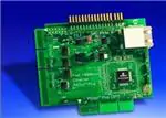
Fast 100 Mbps Ethernet PICtail™ Plus Daughter Board
Overview
The Fast 100 Mbps Ethernet PICtail™ Plus Daughter Board (AC164132) is an Ethernet
demonstration board for evaluating Microchip Technology’s ENC424J600 and ENC624J600
stand-alone 10/100 Ethernet controllers. It is an expansion board compatible with many
PICtail and PICtail Plus host boards, including the Explorer 16, PIC32 I/O Expansion Board,
PICDEM.net™ 2 and PIC18 Explorer development boards.
Features
• ENC624J600 10/100 Ethernet Controller with factory preprogrammed MAC address (see
“ENC424J600/624J600 Data Sheet” (DS39935) for additional information)
• 25 MHz oscillator and integrated magnetic RJ-45 connector
• PICtail Plus Daughter Board edge contacts for SPI or PSP connection to Explorer 16 and
PIC32 I/O Expansion Boards
• PICtail Daughter Board headers for SPI connection to PICDEM.net 2 and PIC18 Explorer
Boards
• Configuration jumpers for PSP Modes 1, 2, 3, 4, 5, 6, 9 and 10 under PMP control with
automatic pinout remapping
• Current monitoring jumper
• Ethernet crossover switches
• 3.3V LDO regulator with shutdown for very low Sleep current
• 3.3V to 5V SPI level translation for the PIC18 Explorer
• SSL encryption add-on software CD for the Microchip TCP/IP Stack
Getting Started
The Fast 100 Mbps Ethernet PICtail Plus Daughter Board must be plugged into a Microchip
Explorer 16, PIC32 I/O Expansion Board (with suitable PIC32 Starter Kit), PICDEM.net 2 or
PIC18 Explorer development board. However, before making any connections, ensure that
the JP2, “I SENSE”, jumper has a shunt installed, shorting the two pins.
The connection to the host motherboard differs based on the interface mode desired and
motherboard type.
Explorer 16
For purposes of getting started, use the ENC624J600 in SPI mode. To do this, insert the
Fast 100 Mbps Ethernet PICtail Plus J2 side edge contacts into the topmost position of
the J5 slot on the Explorer 16. Pin 1 on J2 of the PICtail Daughter Board should align with
Pin 1 on J5 of the Explorer 16. The Ethernet cable will connect to the PICtail Daughter
Board on the side closest to the Explorer 16 Board’s four push buttons.
PIC32 I/O Expansion Board
The PIC32 I/O Expansion Board is very similar to the Explorer 16. If using a
PIC32MX360F512L based Starter Kit, insert the Fast 100 Mbps Ethernet PICtail Plus J2
side edge contacts into the topmost position of the J4 or J2 slots on the PIC32 I/O Expansion Board. Pin 1 of J2 on the PICtail Daughter Board should align with the Pin 1 slot on
the PIC32 I/O Expansion Board. If using a PIC32MX460F512L based PIC32 USB Starter
Board, insert the PICtail Daughter Board’s J2 connector into the middle position of J4 or
J2. This will result in Pin 1 of J2 on the PICtail Daughter Board aligning with Pin 33 on the
PIC32 I/O Expansion Board.
PICDEM.net 2
The PICDEM.net 2 uses the PICtail Daughter Board thru-hole headers to interface using
SPI mode. To make this connection, insert the Fast 100 Mbps Ethernet PICtail Plus J4
right angle header into the J5 female header on the PICDEM.net 2. Pin 1 on J4 of the
PICtail Daughter Board, labeled “RE2”, must align with Pin 1 on J5 of the PICDEM.net 2
(also labeled “RE2”). This correct orientation does not connect the 2x3 J3 header to
anything. The Ethernet cable will enter the PICtail Daughter Board from the same
PICDEM.net 2 board edge that contains the two 10Base-T Ethernet jacks.
1
�PIC18 Explorer
The PIC18 Explorer uses the PICtail Daughter Board thru-hole headers to interface using
SPI mode, much like the PICDEM.net 2 connection. Insert the Fast 100 Mbps Ethernet
PICtail Plus Daughter Board J3 and J4 right angle headers into the J9 and J3 female
headers on the PIC18 Explorer, respectively. Pin 1 on J3 of the PICtail Daughter Board,
labeled “ADJ”, must align with Pin 1 on J9 of the PIC18 Explorer (also labeled “ADJ”).
After appropriately connecting the PICtail Daughter Board to the host motherboard, apply
power to the host motherboard. If an Ethernet cable is attached and a link partner is also
attached at the far end of the cable, the green Ethernet link status LED will automatically
turn on. The orange or amber RX/TX activity LED will also blink if Ethernet traffic is sent to
the PICtail Daughter Board. If the link LED does not light as expected, it is possible that the
TX and RX Ethernet data pairs are swapped. To test this, a crossover Ethernet cable could
be used, or appropriate firmware may be written, to toggle the MDIX control signal which will
swap the TX and RX data pairs on the PICtail Daughter Board.
Further evaluation will require the use of a TCP/IP Stack software library running on the host
motherboard to appropriately control the Ethernet interface. Microchip TCP/IP Stack,
Version 5.00 and later, can be used with this PICtail Daughter Board. The latest Microchip
TCP/IP Stack version should be downloaded from the Microchip web site at
www.microchip.com/tcpip. After obtaining and installing the stack, further getting started
information is available in the TCP/IP Stack Help. Instead of building the stack, it is strongly
recommended that first time testing be done using one of the stack’s precompiled .hex
files, if available, for the hardware and interface mode in use.
Schematic and Bill of Materials
The Fast 100 Mbps Ethernet PICtail Plus schematic and bill of materials are not provided
here. They may be obtained from the Microchip web site at www.microchip.com/ethernet or
by installing the latest Microchip TCP/IP Stack available from www.microchip.com/tcpip.
Jumper Configuration
The Fast 100 Mbps Ethernet PICtail Plus board has seven jumpers that control the operational mode of the ENC624J600 and enable various features. The jumper functions are
summarized in the following table:
Jumper Functions
Jumper
Type
Description
JP2
Bridge
JP3
Bridge
ENC624J600 CLKOUT Enable to PICtail Interface
JP7
Bridge
PIC® MCU PMP PMA to ENC624J600 AD
Connection Enable
JP8
Bridge
PIC MCU PMP PMA to ENC624J600 A
Connection Enable
ENC624J600 Power Control and Current Sense
JP9
2-Way
ENC624J600 PSPCFG2 and Pinout Control
JP10
2-Way
ENC624J600 PSPCFG3 and Pinout Control
JP11
2-Way
ENC624J600 PSPCFG1/PSPCFG4 and Pinout Control
JP2
JP2 lies directly in series with the +3.3V power supply for the ENC624J600 and Ethernet
magnetics (3V3ETH). To power the ENC624J600 from an external source, remove the JP2
shunt and connect an external power supply to the red 3V3ETH Test Point (TP2). To
measure the ENC624J600 and magnetics current usage, replace the JP2 shunt with a current meter. Because the Ethernet solution will draw in excess of 200 mA when all features
are enabled, apply caution before attempting to measure the current using a 200 mA fused
current measurement scale, available on many handheld multimeters.
For normal device operation, JP2 must be shorted by a jumper shunt.
2
�JP3
JP3, when shorted, will connect the ENC624J600 CLKOUT signal, after level shifting, to the
PICtail connector (J4 Pin 5). If using the PIC18 Explorer, this function may be used to clock
the PIC MCU via the OSC1 input. However, care must be taken to avoid violating the specifications of the Y1 crystal on the PIC18 Explorer. Ideally, the Y1 crystal should be removed,
leaving the crystal soldered on will likely still work, but could force excessive current through
the crystal, potentially damaging it.
Pin 5 of the PICtail Daughter Board interface is not connected on the PICDEM.net 2, so the
state of JP3 will have no impact when using this host board.
If JP3 is left open, the leftmost pin (closest to the ‘C’ in “CLKOUT” on the board silkscreen)
can be used as a convenient test point for measuring or using the ENC624J600 CLKOUT
signal. Note, though, that this signal is level shifted by the U4 buffer, so the peak voltage will
match the VPIC power supply (V_VAR for PIC18 Explorer, +5V for PICDEM.net 2).
The default state of JP3 is open (no jumper shunt).
JP7-JP11
JP7-JP11 control the pinout of the J1 PICtail Plus Daughter Board edge contacts required
for the various Parallel Interface modes. If using the SPI interface, the states of JP7-JP11
are all unimportant. However, to avoid floating the ENC624J600 PSPCFGx input pins, it is
recommended that the JP9-JP11 jumpers have a shunt installed at all times in either the 3V3
or GND configuration.
If using a Parallel Interface mode, set the jumpers according to the desired mode.
Parallel Interface Mode Jumper Settings
PSP Mode
PMA
to AD
PMA
to A
PSPCFG1&4
PSPCFG2
PSPCFG3
1 (8-bit)
—
Short
GND
GND
GND
2 (8-bit)(1)
—
Short
3V3
GND
GND
3 (16-bit)
—
Short
GND
3V3
GND
4 (16-bit)(1)
—
Short
3V3
3V3
GND
5 (8-bit MUX)
Short
—
GND
GND
3V3
6 (8-bit MUX)(1)
Short
—
3V3
GND
3V3
9 (16-bit MUX)
—
—
GND
3V3
3V3
10 (16-bit MUX)(1)
—
—
3V3
3V3
3V3
Legend:
— = open; Short = shunt installed; GND = middle and GND peg shorted;
3V3 = middle and 3V3 peg shorted
Note 1:
Do not use PSP Modes 2, 4, 6 or 10 with the Explorer 16. Bus contention
with the Explorer 16 LCD will occur.
For convenient access, this table is also printed on the backside of the Fast 100 Mbps
Ethernet PICtail Plus.
The prior table assumes that Direct Addressing mode is used (all address lines are connected). For Indirect Addressing modes, with a minimal number of address lines connected,
leave the JP7 (PMA to AD) and JP8 (PMA to A) jumpers open.
Since the pinout changes with the different jumper settings, refer to the “Signal Interface”
section for the associated connections that are required.
3
�Signal Interface
The pinout of the Fast 100 Mbps Ethernet PICtail Plus depends upon the jumper settings
and which physical connector is used.
PICtail Daughter Board Dual Row Right Angle Header (J3, J4, J5)
The J3 and J4 headers are designed to provide an SPI interface to the PIC18 Explorer and
PICDEM.net 2 Development Boards. The J5 connector is not used; holes for J5 are present
only to aid physical alignment. The PICtail Daughter Board is not wired to permit the
ENC624J600 to interface to the PIC18 Explorer or PICDEM.net 2 using any Parallel modes.
When using the PICtail Daughter Board header, the pinout is as shown in the following table:
Pinout for the PICtail™ Daughter Board Header
Signal Name on Board
J3
Pin
J4
Pin
PICtail™
Daughter
Board
—
4
5VEXT
+5V
—
5V Power
—
5
GND
GND
—
Ground Reference
5
—
OSC1_PIC
OSC1
—
CLKOUT to PIC® MCU (optional)(1)
Function
PIC18
PICDEM.net™ 2
Explorer
8
—
SI/RD/RW
RC5/SDO1
10
—
SO_VPIC
RC4/SDI1
SPI Data to PIC MCU
12
—
SCK/AL
RC3/SCK1
SPI Clock from PIC MCU
17
—
SHDN
RB5
Shutdown from PIC MCU
19
—
MDIX
RB4
Ethernet Crossover from PIC MCU
21
—
CS/CS
RB3
23
—
INT_VPIC
RB2/INT2
26
—
VPIC
28
—
Note 1:
GND
V_VAR
SPI Data from PIC MCU
SPI Chip Select from PIC MCU
+5V
GND
Interrupt to PIC MCU
5V Power
Ground Reference
To enable CLKOUT, JP3 must be shorted.
If using the PIC18 Explorer with a PIM installed, be sure to check the PIM schematics for
any renamed or remapped pins.
PICtail Plus (SPI, J2)
The J2 board edge contacts are designed to provide an SPI interface to the Explorer 16 and
PIC32 I/O Expansion Boards. The J2 board edge is keyed such that there are only three
possible ways to insert it into the Explorer 16 and PIC32 I/O expansion slot:
1. Pin 1 on J2 aligns with Pin 1 on host motherboard – use SPI1 pinout.
2. Pin 1 on J2 aligns with Pin 33 on host motherboard – use SPI2 pinout.
3. Pin 1 on J2 aligns with Pin 94 on host motherboard – illegal, do not connect.
4
�SPI1
If the PICtail Daughter Board is mated to the topmost SPI1 slot on the Explorer 16 or PIC32
I/O Expansion Board, the following connections will be made:
SPI1 Mating Connections
Signal Name on Board
J2
Pin
Mating
Pin
3
3
SCK/AL
5
5
SO/WR/WRL/EN RF7/SDI1_E
Function
PICtail™
Explorer 16 and
Daughter Board PIC32 I/O Exp.
RF6/SCKI
SPI Clock from PIC® MCU
SPI Data to PIC MCU
7
7
SI/RD/RW
RF8/SDO1_E
9, 10
9, 10
GND
GND
SPI Data from PIC MCU
Ground Reference
13
13
MDIX
RB3/AN3
Ethernet Crossover from PIC MCU
15, 16
15, 16
GND
GND
Ground Reference
17
17
INT/SPISEL
RE9/INT2
Interrupt to PIC MCU
19
19
CS/CS
RD14/U1CTS_E
SPI Chip Select from PIC MCU
20
20
SHDN
RD15/U1RTS_E
Shutdown from PIC MCU
23, 24
23, 24
+5V
+5V
5V Power
If using the PIC32 I/O Expansion Board with a PIC32 USB Starter Board (Rev B), do not
plug the PICtail Daughter Board into the SPI1 slot. The RD14/U1CTS signal is routed on the
starter board to USB power control circuitry and will cause bus contention with the
ENC624J600 chip select signal.
SPI2
If the PICtail Daughter Board is mated to the middle SPI2 slot on the Explorer 16 or PIC32
I/O Expansion Board, the following connections will be made:
SPI2 Mating Connections
Signal Name on Board
J2
Pin
Mating
Pin
3
35
SCK/AL
5
37
SOWR/WRL/EN RG7/PMPA4/SDI2
39
SI/RD/RW
7
9, 10
13
PICtail™
Daughter Board
41, 42 GND
45
MDIX
15, 16 47, 48 GND
Function
Explorer 16 and
PIC32 I/O Exp.
RG6/PMPA2/SCK2
SPI Clock from PIC® MCU
SPI Data to PIC MCU
RG8/PMPA3/SDO2
SPI Data from PIC MCU
GND
Ground Reference
RA9/PMPA7
Ethernet Crossover from PIC MCU
GND
Ground Reference
17
49
INT/SPISEL
RA15/INT4
Interrupt to PIC MCU
19
51
CS/CS
RF12/U2CTS
SPI Chip Select from PIC MCU
20
52
SHDN
RF13/U2RTS
Shutdown from PIC MCU
+5V
5V Power
23, 24 55, 56 +5V
Note that Explorer 16 and PIC32 I/O Exp. signal names are with respect to the Explorer 16
schematic, which assumes the use of a PIC24FJ128GA010 PIM. Various other PIMs
(e.g., PIC32MX460F512L) have a different pinout, making several of the pin names listed in
the prior two tables inaccurate. Always check the PIM or PIC32 processor board
schematics, or documentation to ensure that the signals have not been rewired.
5
�PICtail Plus (Parallel, J1)
The J1 board edge contacts are available for evaluating the ENC624J600 device’s Parallel
Interface modes. Due to the large number of pins required to support a parallel interface,
only the Explorer 16 and PIC32 I/O Expansion Boards are set up to use this feature. The
pinout of the J1 connector is set up to be driven by the host microcontroller via the Parallel
Master Port (PMP) peripheral available on select processors. In some cases, where the
PMP peripheral or necessary mode is unavailable, it is possible to bit-bang the parallel interface at reduced performance. However, in other cases where not all of the necessary pins
are connected, it is infeasible to use the J1 parallel interface and use of the J2 SPI
connector is required instead.
Even when a host processor has all of the necessary pins, there are various limitations due
to pin multiplexing performed on the host motherboard. At the time of the Fast 100 Mbps
Ethernet PICtail Plus product development, there are several known issues:
• On the Explorer 16, it is not possible to use the LCD module with the ENC624J600 in
Parallel mode. The LCD interfaces to the same PMP lines as required for the
ENC624J600; however, unlike the ENC624J600, the LCD does not include a chip select
line. Therefore, it remains listening on the parallel bus at all times and all communications
to/from the ENC624J600 also get processed by the LCD controller.
• On the Explorer 16, PSP Modes 2, 4, 6 and 10 must not be used. For these interface
modes, any read operation from the ENC624J600 will simultaneously cause a read from
the LCD, causing bus contention. To avoid this, the RD5/PMPRD signal on the
Explorer 16 must be disconnected from the LCD. The LCD R/W input should then be tied
to VSS to force it into Write mode at all times.
• On the Explorer 16, PSP Modes 3 and 4 should not be used. For these 16-Bit
Demultiplexed modes, the Explorer 16 board’s U5 25LC256 EEPROM may become
selected and cause bus contention or EEPROM data corruption while communicating
with the ENC624J600. The EEPROM must be removed from the board to avoid this
potential problem.
• On the Explorer 16, the RF4/PMPA9/U2RX and RF5/PMPA8/U2TX pins have UART2
peripheral features multiplexed onto the same pins, as required for the PMP Address 9
and 8 control lines. Therefore, in PSP Modes 1-6, with full direct addressing capability, the
Explorer 16 board’s RS-232 COM port (P1) cannot be used. However, with indirect
addressing, the UART is still available.
• On the Explorer 16, the D8 LED cannot be used. The RA5/TDO control signal connected
to D8 is used as the chip select control signal to the ENC624J600.
• On the Explorer 16, when using PSP Modes 3, 4, 9 or 10 (all 16-bit modes), the S4, S3
and S6 push buttons cannot be used while communicating with the ENC624J600. The I/O
pins used for these buttons are required for PMD13, PMD14 and PMD15, respectively.
• On the PIC32 Starter Kit (Rev C) and PIC32 USB Starter Board (Rev B) for the PIC32 I/O
Expansion Board, the S1, S2 and S3 push buttons short the PMPD14, PMPD15 and
PMPD13 signals to GND. As a result, when the processor is communicating to the
ENC624J600 using PSP Modes 3, 4, 9 or 10 (all 16-bit modes), these push buttons cannot be used. Also, since the buttons short the pins directly to GND without current limiting
resistors, users must not push any of the buttons during communications as this will
cause bus contention and corrupt communications with the ENC624J600.
Other compatibility restrictions may exist and may be created in the future for new PIMs and
PIC32 starter boards. Be sure to check the appropriate schematics of all involved
components to ensure compatibility.
6
�All PSP Modes
The J1 parallel interface connector has several fixed power and control signals that apply to
all PSP modes and do not change, regardless of the jumper settings. These common
signals are shown below:
Common Signal Connections for All PSP Modes
Signal Name on Board
J1
Pin
PICtail™
Daughter Board
Function
Explorer 16 and
PIC32 I/O Exp.
13
MDIX
RB3/AN3
Ethernet Crossover from PIC® MCU
17
INT/SPISEL
RE/INT2
Interrupt to PIC MCU
23, 24
+5V
+5V
5V Power
41
GND
GND
Ground Reference
SPISEL Pull-Down for PSP
PSPSEL_VSS
GND
47, 48
42
GND
GND
Ground Reference
55, 56
+5V
+5V
5V Power
72
CS
RA5/TDO
Chip Select from PIC MCU
85
SHDN
119, 120 GND
RC1
Shutdown from PIC MCU
GND
Ground Reference
7
�PSP Modes 1 and 2
For PSP Mode 1 (PSPCFG1/4 = PSPCFG2 = PSPCFG3 = GND) and PSP Mode 2
(PSPCFG1/4 = VDD, PSPCFG2 = PSPCFG3 = GND) with direct addressing (PMA to A
shorted), the ENC624J600 PSP interface signals are connected as follows:
Interface Signal Connections for PSP Modes 1 and 2 (Direct Addressing)
Signal Name
J1
Pin
ENC624J600
Function
Address from PIC® MCU
33
A2
RG9/PMPA2/SS2
34
A9
RF4/PMA9/U2RX
Address from PIC MCU
35
A5
RG6/PMPA5/SCK2
Address from PIC MCU
36
A8
RF5/PMA8/U2TX
Address from PIC MCU
37
A4
RG7/PMPA4/SDI2
Address from PIC MCU
Address from PIC MCU
39
A3
RG8/PMPA3/SDO2
45
A7
RA9/PMPA7
Address from PIC MCU
46
A6
RA10/PMPA6
Address from PIC MCU
79
A13
RB10/PMA13
Address from PIC MCU
80
A12
RB11/PMA12
Address from PIC MCU
81
A11
RB12/PMA11
Address from PIC MCU
82
A10
RB13/PMA10
Address from PIC MCU
83
A1
RB14/PMPA1
Address from PIC MCU
84
A0
RB15/PMPA0
Address from PIC MCU
97
WR(1) or EN(2)
RD4/PMPWR
Write(1) or Enable(2) Strobe from PIC
MCU
98
RD(1) or R/W(2)
RD5/PMPRD
Read Strobe(1) or Read/Write(2) Select
from PIC MCU
104
AD14
RD11/PMPCS1
Address from PIC MCU
RE0/PMPD0RE7/PMPD7
Bidirectional Data
109-116 AD0-AD7
Note 1:
PSP Mode 1.
2:
PSP Mode 2.
8
Explorer 16 and
PIC32 I/O Exp.
�When jumpered for indirect addressing (PMA to A is open), the ENC624J600 PSP
connections simplify to the following:
Interface Signal Connections for PSP Modes 1 and 2 (Indirect Addressing)
Signal Name
J1
Pin
ENC624J600
Explorer 16 and
PIC32 I/O Exp.
Function
33
A2
RG9/PMPA2/SS2
Address from PIC® MCU
35
A5
RG6/PMPA5/SCK2
Address from PIC MCU
37
A4
RG7/PMPA4/SDI2
Address from PIC MCU
39
A3
RG8/PMPA3/SDO2
Address from PIC MCU
45
A7
RA9/PMPA7
Address from PIC MCU
46
A6
RA10/PMPA6
Address from PIC MCU
83
A1
RB14/PMPA1
Address from PIC MCU
84
A0
RB15/PMPA0
Address from PIC MCU
97
WR(1) or EN(2)
RD4/PMPWR
Write(1) or Enable(2) Strobe from PIC
MCU
98
RD(1) or R/W(2)
RD5/PMPRD
Read Strobe(1) or Read/Write(2) Select
from PIC MCU
104
A8
RD11/PMPCS1
Address from PIC MCU
RE0/PMPD0RE7/PMPD7
Bidirectional Data
109-116 AD0-AD7
Note 1:
PSP Mode 1.
2:
PSP Mode 2.
Note that for the indirect PSP Modes 1 and 2, the ENC624J600 A8 address line is
connected to RD11/PMPCS1 (PMP address line A14). This necessitates slightly unusual
usage of the PMP module with address translation required in the application firmware.
However, this translation can be performed at compile time, resulting in no run-time
performance degradation. By not using the RF5/PMA8/U2TX pin for this address bit, the
PIC MCU’s UART2 module can still be used.
When indirect addressing is selected, the unconnected ENC624J600 A9-A14 address lines
are automatically pulled high by pull-up resistors on the PICtail Daughter Board. A fixed
application could tie these pins directly to VDD without the use of resistors.
9
�PSP Modes 3 and 4
For PSP Mode 3 (PSPCFG2 = VDD, PSPCFG1/4 = PSPCFG3 = GND) and PSP Mode 4
(PSPCFG1/4 = PSPCFG2 = VDD, PSPCFG3 = GND) with direct addressing (PMA to A
shorted), the ENC624J600 PSP interface signals are connected as follows:
Interface Signal Connections for PSP Modes 3 and 4 (Direct Addressing)
Signal Name
J1
Pin
27
ENC624J600
AD8
Function
RG0 (PMPD8)
Bidirectional Data
Bidirectional Data
28
AD11
RF0 (PMPD11)
29
AD9
RG1 (PMPD9)
Bidirectional Data
30
AD10
RF1 (PMPD10)
Bidirectional Data
33
A2
RG9/PMPA2/SS2
Address from PIC® MCU
34
A9
RF4/PMA9/U2RX
Address from PIC MCU
35
A5
RG6/PMPA5/SCK2
Address from PIC MCU
36
A8
RF5/PMA8/U2TX
Address from PIC MCU
37
A4
RG7/PMPA4/SDI2
Address from PIC MCU
39
A3
RG8/PMPA3/SDO2
Address from PIC MCU
45
A7
RA9/PMPA7
Address from PIC MCU
46
A6
RA10/PMPA6
Address from PIC MCU
79
A13
RB10/PMA13
Address from PIC MCU
80
A12
RB11/PMA12
Address from PIC MCU
81
A11
RB12/PMA11
Address from PIC MCU
82
A10
RB13/PMA10
Address from PIC MCU
83
A1
RB14/PMPA1
Address from PIC MCU
84
A0
RB15/PMPA0
97
WRL & WRH(1) or RD4/PMPWR
B0SEL & B1SEL(2)
16-Bit Write(1) or Both Byte Select(2)
Strobes from PIC MCU
98
RD(1) or R/W(2)
16-Bit Read Strobe(1) or Read/Write(2)
Select from PIC MCU
RD5/PMPRD
Address from PIC MCU
99
AD14
RD6 (PMPD14)
Bidirectional Data
100
AD15
RD7 (PMPD15)
Bidirectional Data
105
AD12
RD12 (PMPD12)
Bidirectional Data
106
AD13
RD13 (PMPD13)
Bidirectional Data
RE0/PMPD0RE7/PMPD7
Bidirectional Data
109-116 AD0-AD7
Note 1:
PSP Mode 3.
2:
PSP Mode 4.
10
Explorer 16 and
PIC32 I/O Exp.
�The PICtail Daughter Board has the WRL/B0SEL signal connected to WRH/B1SEL, so only
16-bit word writes are possible. Writes to the high or low byte, individually, cannot be
performed.
When jumpered for indirect addressing (PMA to A is open), the ENC624J600 PSP
connections simplify to the following:
Interface Signal Connections for PSP Modes 3 and 4 (Indirect Addressing)
Signal Name
J1
Pin
ENC624J600
Explorer 16 and
PIC32 I/O Exp.
Function
27
AD8
RG0 (PMPD8)
28
AD11
RF0 (PMPD11)
Bidirectional Data
Bidirectional Data
29
AD9
RG1 (PMPD9)
Bidirectional Data
30
AD10
RF1 (PMPD10)
Bidirectional Data
33
A2
RG9/PMPA2/SS2
Address from PIC® MCU
Address from PIC MCU
35
A5
RG6/PMPA5/SCK2
37
A4
RG7/PMPA4/SDI2
Address from PIC MCU
39
A3
RG8/PMPA3/SDO2
Address from PIC MCU
45
A7
RA9/PMPA7
Address from PIC MCU
46
A6
RA10/PMPA6
Address from PIC MCU
83
A1
RB14/PMPA1
Address from PIC MCU
84
A0
RB15/PMPA0
Address from PIC MCU
(1)
97
WRL & WRH or RD4/PMPWR
B0SEL & B1SEL(2)
16-Bit Write(1) or Both Byte Select(2)
Strobes from PIC MCU
98
RD(1) or R/W(2)
RD5/PMPRD
16-Bit Read Strobe(1) or Read/Write(2)
Select from PIC MCU
99
AD14
RD6 (PMPD14)
Bidirectional Data
100
AD15
RD7 (PMPD15)
Bidirectional Data
105
AD12
RD12 (PMPD12)
Bidirectional Data
106
AD13
RD13 (PMPD13)
Bidirectional Data
RE0/PMPD0RE7/PMPD7
Bidirectional Data
109-116 AD0-AD7
Note 1:
PSP Mode 3.
2:
PSP Mode 4.
11
�PSP Modes 5 and 6
For PSP Mode 5 (PSPCFG1/4 = PSPCFG2 = GND, PSPCFG3 = VDD) and PSP Mode 6
(PSPCFG1/4 = PSPCFG3 = VDD, PSPCFG2 = GND) with direct addressing (PMA to AD
shorted), the ENC624J600 PSP interface signals are connected as follows:
Interface Signal Connections for PSP Modes 5 and 6 (Direct Addressing)
Signal Name
J1
Pin
34
ENC624J600
AD9
RF4/PMA9/U2RX
Function
Address from PIC® MCU
36
AD8
RF5/PMA8/U2TX
Address from PIC MCU
79
AD13
RB10/PMA13
Address from PIC MCU
80
AD12
RB11/PMA12
Address from PIC MCU
81
AD11
RB12/PMA11
Address from PIC MCU
82
AD10
RB13/PMA10
Address from PIC MCU
84
AL
RB15/PMPA0
Address Latch from PIC MCU
97
WR(1) or EN(2)
RD4/PMPWR
Write(1) or Enable(2) Strobe from PIC
MCU
98
RD(1) or R/W(2)
RD5/PMPRD
Read Strobe(1) or Read/Write(2) Select
from PIC MCU
104
AD14
RD11/PMPCS1
Address from PIC MCU
RE0/PMPD0RE7/PMPD7
Address from PIC MCU and
Bidirectional Data
109-116 AD0-AD7
Note 1:
PSP Mode 5.
2:
PSP Mode 6.
12
Explorer 16 and
PIC32 I/O Exp.
�When jumpered for indirect addressing (PMA to AD is open), the ENC624J600 PSP
connections simplify to the following:
Interface Signal Connections for PSP Modes 5 and 6 (Indirect Addressing)
Signal Name
J1
Pin
ENC624J600
Explorer 16 and
PIC32 I/O Exp.
Function
84
AL
RB15/PMPA0
Address Latch from PIC® MCU
97
WR(1) or EN(2)
RD4/PMPWR
Write(1) or Enable(2) Strobe from PIC
MCU
98
RD(1) or R/W(2)
RD5/PMPRD
Read Strobe(1) or Read/Write(2) Select
from PIC MCU
104
AD8
RD11/PMPCS1
Address from PIC MCU
RE0/PMPD0RE7/PMPD7
Address from PIC MCU and
Bidirectional Data
109-116 AD0-AD7
Note 1:
PSP Mode 5.
2:
PSP Mode 6.
Like indirect PSP Modes 1 and 2, the indirect PSP Modes 5 and 6 have the ENC624J600
Address Line 8 connected to RD11/PMPCS1 instead of RF5/PMA8/U2TX to allow the
UART2 module to be used concurrently.
Of all possible parallel combinations, PSP Modes 5 and 6, with indirect addressing, use the
least I/O pins, but still provide very respectable performance. With minimal I/O pins used, it
is the least likely combination to have multiplexed board and processor features causing
unexpected behavior. It, therefore, should be the starting point when evaluating the
ENC624J600 device’s parallel interface for the first time. When using PSP Modes 5 and 6,
the ENC624J600 behavior is representative of the lower pin count ENC424J600, which only
supports SPI and PSP Modes 5 and 6.
13
�PSP Modes 9 and 10
For PSP Mode 9 (PSPCFG1/4 = GND, PSPCFG2 = PSPCFG3 = VDD) and PSP Mode 10
(PSPCFG1&4 = PSPCFG2 = PSPCFG3 = VDD), the ENC624J600 PSP interface signals are
connected as follows:
Interface Signal Connections for PSP Modes 9 and 10
Signal Name
J1
Pin
ENC624J600
Explorer 16 and
PIC32 I/O Exp.
Function
27
AD8
RG0 (PMPD8)
Address from PIC MCU and
Bidirectional Data
28
AD11
RF0 (PMPD11)
Address from PIC MCU and
Bidirectional Data
29
AD9
RG1 (PMPD9)
Address from PIC MCU and
Bidirectional Data
30
AD10
RF1 (PMPD10)
Address from PIC MCU and
Bidirectional Data
84
AL
RB15/PMPA0
Address Latch from PIC MCU
(1)
97
WRL & WRH or RD4/PMPWR
B0SEL & B1SEL(2)
16-Bit Write(1) or Both Byte Select(2)
Strobes from PIC MCU
98
RD(1) or R/W(2)
RD5/PMPRD
16-Bit Read Strobe(1) or Read/Write(2)
Select from PIC MCU
99
AD14
RD6 (PMPD14)
Bidirectional Data
100
AD15
RD7 (PMPD15)
Bidirectional Data
105
AD12
RD12 (PMPD12)
Address from PIC MCU and
Bidirectional Data
106
AD13
RD13 (PMPD13)
Address from PIC MCU and
Bidirectional Data
RE0/PMPD0RE7/PMPD7
Address from PIC MCU and
Bidirectional Data
109-116 AD0-AD7
Note 1:
2:
PSP Mode 9.
PSP Mode 10.
For PSP Modes 9 and 10, the 16-bit bidirectional data is carried by the PMPD0-PMPD15 I/O
pins. This requires that all 16 pins be connected. Since the entire 14-bit address bus is
multiplexed onto these same pins, the concept of indirect addressing using a limited set of
address pins is unnecessary. When using PSP Mode 9 or 10, direct addressing is always
performed.
14
�Board Design Theory
Automatic Parallel Interface Pinout Changes
U1, U2, U3, U5, U13 and U14 are bus switches and glue logic for the purpose of changing
the pinout of the parallel PICtail Plus board edge contacts. They are unnecessary and
should be omitted in ordinary application circuits as the appropriate SPI or PSP interface
pins, between the host processor and ENC424J600/624J600, can be directly connected.
Power Supply and Shutdown
U7 and its surrounding components form a 3.3V regulated power supply with shutdown
capability. When plugged into a PICDEM.net 2, only a single 5V power supply is available.
The MCP1825 LDO regulator supplies the needed 3.3V power for the ENC624J600,
associated pull up resistors and the Ethernet magnetics. Because the ENCX24J600 draws
considerable current in Sleep mode, it is beneficial in some applications to completely disconnect power from the ENCX24J600 and magnetics instead of using the ENCX24J600
Sleep feature.
Disconnecting power can be achieved by means of the SHDN signal. Care must be taken in
software to also tri-state or drive all SPI/PSP interface signals to GND when power is
removed to avoid having current enter the ENCX24J600 through the I/O pins.
If an application circuit already has a regulated 3.3V supply available, the MCP1825 can be
replaced with a MOSFET to achieve the same shutdown functionality at lower cost, as
shown in the following diagram. When using a MOSFET, the C6 and C7 capacitors would be
unnecessary.
Replacing MCP1825 with a MOSFET
+3.3V
100
kΩ
100kO
SHDN
S
G
Si1307DL
D
3V3ETH
If using a circuit like this, be sure to power all ENCX24J600 VDD pins and the center tap of
the Ethernet TX transformer through this power switch. It is invalid to disconnect VDD without
removing power from the magnetics.
Ethernet Auto-Crossover
U8 is a quad 2:1 multiplexer bus switch capable of passing analog signals bidirectionally. Its
purpose is to swap the TPOUT+/- interface pins with the TPIN+/- interface pins to the RJ-45
connector at run time under software control. If the user plugs in a crossover Ethernet cable
when a straight through cable is required, or vice versa, the software can automatically swap
the two data pairs via the MDIX signal. This feature permits a true plug-and-play experience
for users who may not be aware of the internal differences between a crossover cable and a
straight cable.
When MDIX is held low (MDI state), the TPOUT+/- signals are routed to Pins 1 and 2 at the
RJ-45 connector, while the TPIN+/- signals are routed to Pins 3 and 6, respectively. These
connections are the ordinary default required for end devices. When MDIX is pulled high
(MDIX state), the TPOUT+/- signals are routed to Pins 3 and 6, while the TPIN+/- signals
appear on Pins 1 and 2, respectively, of the RJ-45 connector. In this state, the wires are
crossed as a crossover cable would do externally.
15
�The Microchip TCP/IP Stack software automatically controls the MDIX state (if present) by
randomly toggling the MDIX pin when no Ethernet link is detected. Random timing is used to
ensure that two identical devices powered up at an identical time will not toggle in lock-step
with each other, which would never converge on the correct routing.
If the target application does not need auto-crossover functionality, this feature may be disabled by leaving the MDIX signal tri-stated or by actively driving it low. If complete hardware
removal of this feature is desired, unsolder and remove U8, and install 0Ω resistors at
R10-R12 and R16.
The Fairchild FST3257 was used in this circuit due to its low-cost, low input/output capacitance and low on resistance. Low capacitance and resistance are necessary to ensure that
the switches do not add a significant impedance discontinuity which would distort the highspeed signaling waveform and increase return loss. This circuit was tested to ensure that
the transmit waveform in both 10Base-T and 100Base-TX speeds was not significantly
altered or in violation of the IEEE 802.3™ standards (excluding the noted deviations in the
ENC624J600 silicon errata documentation). Functional receive performance was also tested
under worst case cable lengths of 100 meters.
If implementing a similar circuit in end products, take close note of the +5V power requirements. With 10Base-T signaling, the TPOUT+/- and TPIN+/- Common mode is forced, via
R6, to roughly 3V3ETH – (80mA * 10Ω) or 2.5V nominally, 2.8V max. The 10Base-T
differential signaling adds up to +/-1.4V on top of this Common mode, resulting in a peak
voltage of 4.2V that could be applied to the bus switches. The 100Base-TX signaling will
also result in peak voltages that exceed 3V3ETH, but not as significantly as 10Base-T
mode.
If 5V is not available in the target application, it is possible to create a crude voltage source
by making a change pump off of the ENCX24J600 CLKOUT output, as demonstrated here:
Voltage Source Using the ENCX24J600 CLKOUT Output
+3.3V
~+5V
0.1 µF
10 kkΩ
10
BAV99
0.1 µF
CLKOUT
Most bus switches have extremely low-current requirements, so despite the limited current
sourcing capability of CLKOUT, it can potentially be used to both generate ~5V required for
the bus switches and still be used as a clock source for other circuitry in the application.
16
�PICtail Daughter Board Power Interface
U6, D1 and R4 create a power switching circuit to allow both the PICDEM.net 2 and PIC18
Explorer motherboards to be automatically supported without using jumpers to select
between the two. The +5V net powers almost the entire board, including all bus switches,
and the 3.3V regulator for the Ethernet controller. Unfortunately, obtaining a 5V supply from
the PICtail Daughter Board connectors differs based on the motherboard in use.
For the PICDEM.net 2, 5V is supplied on the VPIC net (J4 Pin 26). However, on the PIC18
Explorer, 5V is always supplied on the 5VEXT net (J3 Pin 4), but only supplied sometimes
on VPIC. If a 3.3V PIM is used on the PIC18 Explorer (e.g., PIC18F87J11), then the VPIC
net is only powered to 3.3V. This potential voltage difference makes it illegal to directly
connect the 5VEXT and VPIC nets together.
When the PIC18 Explorer is used, the D1 shottkey diode provides a minimal voltage drop
between the 5VEXT net and the +5V net required to power the Ethernet circuit. The application of voltage on 5VEXT also turns the U6 P-channel MOSFET off, so no current from the
+5V net flows back into the PIC18 Explorer through the VPIC net.
When the PICDEM.net 2 is used, the 5VEXT net is not connected. 5V power is supplied on
VPIC, which forward biases the body diode in U6, causing the +5V net to begin powering up.
Without being driven, the R4 pull-down resistor on the 5VEXT net drops the gate voltage on
U6 to GND. Partially powering +5V causes the U6 MOSFET to turn on and essentially short
the VPIC and +5V nets together.
The U6 MOSFET could be replaced with another schottky diode, like D1, but the use of a
MOSFET allows a wider motherboard voltage tolerance.
Other Information
To obtain the most recent and complete documentation for this demonstration board,
including:
- Information Sheet
- Board Description
- Board Schematics
- Source Code
- Application Examples
- Links to Web Seminars
please refer to the Microchip web site: www.microchip.com/ethernet
17
�NOTES:
18
�NOTES:
19
�Americas
Asia/Pacific
Europe
Atlanta - 678-957-9614
Boston - 774-760-0087
Chicago - 630-285-0071
Cleveland - 216-447-0464
Dallas - 972-818-7423
Detroit - 248-538-2250
Kokomo - 765-864-8360
Los Angeles - 949-462-9523
Phoenix - 480-792-7200
Santa Clara - 408-961-6444
Toronto - 905-673-0699
Australia - Sydney - 61-2-9868-6733
China - Beijing - 86-10-8528-2100
China - Chengdu - 86-28-8665-5511
China - Hong Kong SAR - 852-2401-1200
China - Nanjing- 86-25-8473-2460
China - Qingdao - 86-532-8502-7355
China - Shanghai - 86-21-5407-5533
China - Shenyang - 86-24-2334-2829
China - Shenzhen - 86-755-8203-2660
China - Wuhan - 86-27-5980-5300
China - Xiamen - 86-592-2388138
China - Xian - 86-29-8833-7252
China - Zhuhai - 86-756-3210040
India - Bangalore - 91-80-3090-4444
India - New Delhi - 91-11-4160-8631
India - Pune - 91-20-2566-1512
Japan - Yokohama - 81-45-471-6166
Korea - Daegu - 82-53-744-4301
Korea - Seoul - 82-2-554-7200
Malaysia - Kuala Lumpur - 60-3-6201-9857
Malaysia - Penang - 60-4-227-8870
Philippines - Manila - 63-2-634-9065
Singapore - 65-6334-8870
Taiwan - Hsin Chu - 886-3-6578-300
Taiwan - Kaohsiung - 886-7-536-4818
Taiwan - Taipei - 886-2-2500-6610
Thailand - Bangkok - 66-2-694-1351
Austria - Weis - 43-7242-2244-39
Denmark - Copenhagen - 45-4450-2828
France - Paris - 33-1-69-53-63-20
Germany - Munich - 49-89-627-144-0
Italy - Milan - 39-0331-742611
Netherlands - Drunen - 31-416-690399
Spain - Madrid - 34-91-708-08-90
UK - Wokingham - 44-118-921-5869
03/26/09
Microchip Technology Inc. • 2355 West Chandler Blvd. • Chandler, AZ 85224-6199
www.microchip.com
The Microchip name and logo and the Microchip logo are registered trademarks of Microchip Technology Incorporated in the
U.S.A. and other countries. PICtail and PICDEM.net are trademarks of Microchip Technology Incorporated in the U.S.A. and
other countries. All other trademarks mentioned herein are property of their respective companies. © 2009, Microchip
Technology Incorporated, Printed in the U.S.A. All Rights Reserved. 07/09
DS51857A
*DS51857A*
�