MCP6N16
Evaluation Board
User’s Guide
2015 Microchip Technology Inc.
DS50002365A
�Note the following details of the code protection feature on Microchip devices:
•
Microchip products meet the specification contained in their particular Microchip Data Sheet.
•
Microchip believes that its family of products is one of the most secure families of its kind on the market today, when used in the
intended manner and under normal conditions.
•
There are dishonest and possibly illegal methods used to breach the code protection feature. All of these methods, to our
knowledge, require using the Microchip products in a manner outside the operating specifications contained in Microchip’s Data
Sheets. Most likely, the person doing so is engaged in theft of intellectual property.
•
Microchip is willing to work with the customer who is concerned about the integrity of their code.
•
Neither Microchip nor any other semiconductor manufacturer can guarantee the security of their code. Code protection does not
mean that we are guaranteeing the product as “unbreakable.”
Code protection is constantly evolving. We at Microchip are committed to continuously improving the code protection features of our
products. Attempts to break Microchip’s code protection feature may be a violation of the Digital Millennium Copyright Act. If such acts
allow unauthorized access to your software or other copyrighted work, you may have a right to sue for relief under that Act.
Information contained in this publication regarding device
applications and the like is provided only for your convenience
and may be superseded by updates. It is your responsibility to
ensure that your application meets with your specifications.
MICROCHIP MAKES NO REPRESENTATIONS OR
WARRANTIES OF ANY KIND WHETHER EXPRESS OR
IMPLIED, WRITTEN OR ORAL, STATUTORY OR
OTHERWISE, RELATED TO THE INFORMATION,
INCLUDING BUT NOT LIMITED TO ITS CONDITION,
QUALITY, PERFORMANCE, MERCHANTABILITY OR
FITNESS FOR PURPOSE. Microchip disclaims all liability
arising from this information and its use. Use of Microchip
devices in life support and/or safety applications is entirely at
the buyer’s risk, and the buyer agrees to defend, indemnify and
hold harmless Microchip from any and all damages, claims,
suits, or expenses resulting from such use. No licenses are
conveyed, implicitly or otherwise, under any Microchip
intellectual property rights.
Trademarks
The Microchip name and logo, the Microchip logo, dsPIC,
FlashFlex, flexPWR, JukeBlox, KEELOQ, KEELOQ logo, Kleer,
LANCheck, MediaLB, MOST, MOST logo, MPLAB,
OptoLyzer, PIC, PICSTART, PIC32 logo, RightTouch, SpyNIC,
SST, SST Logo, SuperFlash and UNI/O are registered
trademarks of Microchip Technology Incorporated in the
U.S.A. and other countries.
The Embedded Control Solutions Company and mTouch are
registered trademarks of Microchip Technology Incorporated
in the U.S.A.
Analog-for-the-Digital Age, BodyCom, chipKIT, chipKIT logo,
CodeGuard, dsPICDEM, dsPICDEM.net, ECAN, In-Circuit
Serial Programming, ICSP, Inter-Chip Connectivity, KleerNet,
KleerNet logo, MiWi, MPASM, MPF, MPLAB Certified logo,
MPLIB, MPLINK, MultiTRAK, NetDetach, Omniscient Code
Generation, PICDEM, PICDEM.net, PICkit, PICtail,
RightTouch logo, REAL ICE, SQI, Serial Quad I/O, Total
Endurance, TSHARC, USBCheck, VariSense, ViewSpan,
WiperLock, Wireless DNA, and ZENA are trademarks of
Microchip Technology Incorporated in the U.S.A. and other
countries.
SQTP is a service mark of Microchip Technology Incorporated
in the U.S.A.
Silicon Storage Technology is a registered trademark of
Microchip Technology Inc. in other countries.
GestIC is a registered trademarks of Microchip Technology
Germany II GmbH & Co. KG, a subsidiary of Microchip
Technology Inc., in other countries.
All other trademarks mentioned herein are property of their
respective companies.
© 2015, Microchip Technology Incorporated, Printed in the
U.S.A., All Rights Reserved.
ISBN: 978-1-63277-461-3
QUALITY MANAGEMENT SYSTEM
CERTIFIED BY DNV
== ISO/TS 16949 ==
DS50002365A-page 2
Microchip received ISO/TS-16949:2009 certification for its worldwide
headquarters, design and wafer fabrication facilities in Chandler and
Tempe, Arizona; Gresham, Oregon and design centers in California
and India. The Company’s quality system processes and procedures
are for its PIC® MCUs and dsPIC® DSCs, KEELOQ® code hopping
devices, Serial EEPROMs, microperipherals, nonvolatile memory and
analog products. In addition, Microchip’s quality system for the design
and manufacture of development systems is ISO 9001:2000 certified.
2015 Microchip Technology Inc.
�Object of Declaration: MCP6N16 Evaluation Board
2015 Microchip Technology Inc.
DS50002365A-page 3
�NOTES:
DS50002365A-page 4
2015 Microchip Technology Inc.
�MCP6N16 EVALUATION BOARD
USER’S GUIDE
Table of Contents
Preface ........................................................................................................................... 7
Introduction............................................................................................................ 7
Document Layout .................................................................................................. 7
Conventions Used in this Guide ............................................................................ 8
Recommended Reading........................................................................................ 9
The Microchip Web Site ........................................................................................ 9
Customer Support ................................................................................................. 9
Revision History .................................................................................................... 9
Chapter 1. Installation and Operation
1.1 Introduction ................................................................................................... 11
1.2 Purpose ........................................................................................................ 11
1.3 Description ................................................................................................... 11
1.3.1 Block Diagram ........................................................................................... 11
1.3.2 Sensor Connector ..................................................................................... 12
1.3.3 Instrumentation Amplifier ........................................................................... 12
1.3.4 VREF ......................................................................................................... 12
1.3.5 Power Supply Connector ........................................................................... 12
1.4 What Does This Kit Contain? ....................................................................... 13
Chapter 2. Installation and Operation
2.1 Introduction ................................................................................................... 15
2.2 Required Tools ............................................................................................. 15
2.2.1 Bench Setup .............................................................................................. 15
2.3 Basic Configurations .................................................................................... 16
2.3.1 Out of the Box Setup ................................................................................. 16
2.3.2 Test Points ................................................................................................ 16
2.3.3 Jumper Settings ........................................................................................ 17
2.4 Detailed Circuit Descriptions ........................................................................ 18
2.4.1 Power Supply ............................................................................................ 18
2.4.2 Sensor Connection .................................................................................... 19
2.4.3 Instrumentation Amplifier ........................................................................... 20
2.4.4 External VREF Circuit ............................................................................... 24
2.4.5 PIC® Analog/Digital Interface .................................................................... 25
Appendix A. Schematic and Layouts
A.1 Introduction .................................................................................................. 27
A.2 Board – Schematic ....................................................................................... 28
A.3 Board – Top Silk .......................................................................................... 29
A.4 Board – Top Copper and Silk ....................................................................... 29
2015 Microchip Technology Inc.
DS50002365A-page 5
�MCP6N16 Evaluation Board User’s Guide
A.5 Board – Top Copper .................................................................................... 30
A.6 Board – Bottom Copper ............................................................................... 30
A.7 Board – Bottom Copper and Silk ................................................................. 31
A.8 Board – Bottom Silk ..................................................................................... 31
Appendix B. Bill of Materials (BOM) ...........................................................................33
Worldwide Sales and Service .....................................................................................36
DS50002365A-page 6
2015 Microchip Technology Inc.
�MCP6N16 EVALUATION BOARD
USER’S GUIDE
USER’S GUIDE
Preface
NOTICE TO CUSTOMERS
All documentation becomes dated, and this manual is no exception. Microchip tools and
documentation are constantly evolving to meet customer needs, so some actual dialogs
and/or tool descriptions may differ from those in this document. Please refer to our web site
(www.microchip.com) to obtain the latest documentation available.
Documents are identified with a “DS” number. This number is located on the bottom of each
page, in front of the page number. The numbering convention for the DS number is
“DSXXXXXXXXA”, where “XXXXXXXX” is the document number and “A” is the revision level
of the document.
For the most up-to-date information on development tools, see the MPLAB IDE online help.
Select the Help menu, and then Topics to open a list of available online help files.
INTRODUCTION
This chapter contains general information that will be useful to know before using the
MCP6N16 Evaluation Board. Items discussed in this chapter include:
•
•
•
•
•
•
Document Layout
Conventions Used in this Guide
Recommended Reading
The Microchip Web Site
Customer Support
Revision History
DOCUMENT LAYOUT
This document describes how to use the MCP6N16 Evaluation Board. The document
is organized as follows:
• Chapter 1. “Product Overview” – Important information about the MCP6N16
Evaluation Board.
• Chapter 2. “Installation and Operation” – Covers the initial set-up of this board,
required tools, board setup and lab equipment connections.
• Appendix A. “Schematic and Layouts” – Shows the schematic and board layouts for the MCP6N16 Evaluation Board.
• Appendix B. “Bill of Materials (BOM)” – Lists the parts used to populate the
MCP6N16 Evaluation Board. Also lists alternate components.
2015 Microchip Technology Inc.
DS50002365A-page 7
�Preface
CONVENTIONS USED IN THIS GUIDE
This manual uses the following documentation conventions:
DOCUMENTATION CONVENTIONS
Description
Arial font:
Italic characters
Initial caps
Quotes
Underlined, italic text with
right angle bracket
Bold characters
N‘Rnnnn
Text in angle brackets < >
Courier New font:
Plain Courier New
Represents
Referenced books
Emphasized text
A window
A dialog
A menu selection
A field name in a window or
dialog
A menu path
MPLAB IDE User’s Guide
...is the only compiler...
the Output window
the Settings dialog
select Enable Programmer
“Save project before build”
A dialog button
A tab
A number in verilog format,
where N is the total number of
digits, R is the radix and n is a
digit.
A key on the keyboard
Click OK
Click the Power tab
4‘b0010, 2‘hF1
Italic Courier New
Sample source code
Filenames
File paths
Keywords
Command-line options
Bit values
Constants
A variable argument
Square brackets [ ]
Optional arguments
Curly brackets and pipe
character: { | }
Ellipses...
Choice of mutually exclusive
arguments; an OR selection
Replaces repeated text
Represents code supplied by
user
2015 Microchip Technology Inc.
Examples
File>Save
Press ,
#define START
autoexec.bat
c:\mcc18\h
_asm, _endasm, static
-Opa+, -Opa0, 1
0xFF, ‘A’
file.o, where file can be
any valid filename
mcc18 [options] file
[options]
errorlevel {0|1}
var_name [,
var_name...]
void main (void)
{ ...
}
DS50002365A-page 8
�Preface
RECOMMENDED READING
This user's guide describes how to use MCP6N16 Evaluation Board. Other useful
documents are listed below. The following Microchip documents are available and
recommended as supplemental reference resources.
• MCP6N16 Data Sheet – “Zero-Drift Instrumentation Amplifier” (DS20005318)
Gives detailed information on the instrumentation amplifier.
• MCP6V11 Data Sheet – “7.5 µA, 80 kHz Zero-Drift Op Amps” (DS20005124)
Gives detailed information on the op amp as VREF buffer amplifier.
• MCP1525 Data Sheet – “2.5V and 4.096V Voltage References” (DS21653)
Gives detailed information on the 2.5V voltage reference IC.
• MCP4018 Data Sheet – “7-Bit Single I2C™ Digital POT with Volatile Memory
in SC70” (DS22147)
Gives detailed information on the digital potentiometer IC.
• AN1258 Application Note – “Op Amp Precision Design: PCB Layout
Techniques” (DS01258)
Discusses methods to minimize thermojunction voltage effects in a PCB design.
THE MICROCHIP WEB SITE
Microchip provides online support via our web site at www.microchip.com. This web
site is used as a means to make files and information easily available to customers.
Accessible by using your favorite Internet browser, the web site contains the following
information:
• Product Support – Data sheets and errata, application notes and sample
programs, design resources, user’s guides and hardware support documents,
latest software releases and archived software
• General Technical Support – Frequently Asked Questions (FAQs), technical
support requests, online discussion groups, Microchip consultant program
member listing
• Business of Microchip – Product selector and ordering guides, latest Microchip
press releases, listing of seminars and events, listings of Microchip sales offices,
distributors and factory representatives
CUSTOMER SUPPORT
Users of Microchip products can receive assistance through several channels:
•
•
•
•
Distributor or Representative
Local Sales Office
Field Application Engineer (FAE)
Technical Support
Customers should contact their distributor, representative or field application engineer
(FAE) for support. Local sales offices are also available to help customers.
Technical support is available through the web site at:
http://www.microchip.com/support.
REVISION HISTORY
Revision A (June 2015)
This is the initial release of this document.
2015 Microchip Technology Inc.
DS50002365A-page 9
�Preface
NOTES:
2015 Microchip Technology Inc.
DS50002365A-page 10
�MCP6N16 EVALUATION BOARD
USER’S GUIDE
Chapter 1. Product Overview
1.1
INTRODUCTION
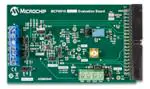
The MCP6N16 Evaluation Board is described by the following:
• Assembly #: 114-00354-R3
• Order #: ADM00640
• Name: MCP6N16 Evaluation Board
This board uses the following Microchip ICs:
•
•
•
•
MCP6N16-100 (Zero-Drift INA)
MCP6V11 (Zero-Drift, Low-Power Op-Amp)
MCP1525 (2.5V Voltage Reference)
MCP4018 (DigiPot Potentiometer, 10 kΩ)
Items discussed in this chapter include:
• Purpose
• Description
• What Does This Kit Contain?
1.2
PURPOSE
This evaluation board is designed to provide an easy and flexible platform when
evaluating the performance of Microchip Technology’s MCP6N16 Zero-Drift
instrumentation amplifier (INA). The fully assembled evaluation board includes
differential input filtering, two jumper selectable gain settings and output filtering, in
addition to an external voltage reference circuit to allow for an adjustable output
common-mode level shifting.
1.3
DESCRIPTION
1.3.1
Block Diagram
Figure 1-1 shows the overall functionality of this evaluation board, followed by a brief
description of each block. Detailed information is available in Appendix
A. “Schematic and Layouts”and Appendix B. “Bill of Materials (BOM)”.
Sensor
Connector
FIGURE 1-1:
2015 Microchip Technology Inc.
INA: MCP6N16
- Single Supply
- Differential Input Filtering
- Output Filter
- Gain Select Option
- Chip-enable
- External V REF
Signal Outputs
(J7, J12)
VREF
- 2.5 Reference Voltage
- Adjustable
- Output Buffer/Filter Op Amp
Power Supply
Connector
(J2)
Overall Block Diagram.
DS50002365A-page 11
�MCP6N16 Evaluation Board User’s Guide
1.3.2
Sensor Connector
The sensor connector, J5, is a 6-pin screw terminal configured to accommodate a
variety of sensors. Bridge-type sensors can have their excitation voltage connected to
either the VDUT supply of the evaluation board or to another externally-supplied source.
In addition, the connector provides sense line connections.
1.3.3
Instrumentation Amplifier
The MCP6N16 is a zero-drift instrumentation amplifier designed for single-supply
operation with rail-to-rail input (no common mode crossover distortion) and output
performance. The device can be operated over a supply range of +1.8V to +5.5V
(VDUT). The evaluation board is populated with the MCP6N16-100, which is designed
to be operated with a gain of +100V/V and higher. At a gain of +100V/V, the
MCP6N16-100 offers a typical input signal range of 34 mVP-P, with a maximum offset
voltage of only 17 µV. It offers a very low noise of 0.93 µVP-P (0.1 to 10 Hz), and a
voltage noise density of 45 nV/√Hz.
The RC input filter provides a low-pass function for both common mode (CM) and
differential mode (DM) signals. They are fast enough to follow supply variations and to
let the MCP6N16 reject CM mains noise (e.g., harmonics of 50 or 60 Hz). In its default
setting, it is set to a gain of +101V/V; using jumper J9, it can be reconfigured for gain
of +301V/V. The output filter provides a low-pass function for both CM and DM signals.
It is slow in order to minimize noise and interference.
1.3.4
VREF
The evaluation board uses the precision voltage reference IC MCP1525 to provide a
+2.5V reference voltage (VREF) with an accuracy of better than 1%. This voltage can
be adjusted and used as an external reference voltage for the MCP6N16 to level shift
its output voltage to a desired level.
1.3.5
Power Supply Connector
The evaluation board allows for a number of supply configurations using connector J2.
In its default configuration, the board can be operated with just one external lab supply
voltage (Jumper J1 is installed and connects the VDUT and VS+ lines together).
Shown in Figure 1-2 and Figure 1-3 are the 3D views of the evaluation board’s top and
bottom side. The evaluation board measures approximately 4.3'' x 2.4''
(10.9 cm x 6.1 cm).
FIGURE 1-2:
DS50002365A-page 12
MCP6N16 Evaluation Board – Top View.
2015 Microchip Technology Inc.
�Product Overview
FIGURE 1-3:
1.4
MCP6N16 Evaluation Board – Bottom View.
WHAT DOES THIS KIT CONTAIN?
The MCP6N16 Evaluation Board kit includes:
• MCP6N16 Evaluation Board (ADM00640)
• Important Information Sheet
2015 Microchip Technology Inc.
DS50002365A-page 13
�MCP6N16 Evaluation Board User’s Guide
NOTES:
DS50002365A-page 14
2015 Microchip Technology Inc.
�MCP6N16 EVALUATION BOARD
USER’S GUIDE
Chapter 2. Installation and Operation
2.1
INTRODUCTION
This chapter shows how to set up and operate the MCP6N16 Evaluation Board. Items
discussed in this chapter include:
• Required Tools
• Basic Configurations
• Detailed Circuit Descriptions
2.2
REQUIRED TOOLS
2.2.1
Bench Setup
In order to operate the evaluation board on the lab bench, the following equipment and
tools are required:
• MCP6N16 Evaluation Board
• Lab DC Power Supply with single output
- Generates +5.0V typical (J2/3, VDUT) and ground (GND, J2/1)
• Voltmeter (Multimeter)
• Signal Generator to simulate a low-level sensor signal, or a suitable sensor
• Oscilloscope with high-impedance probe (≥ MΩ)
• Optional: Signal Analyzer (network analyzer, spectrum analyzer, etc.)
- High-input impedance (≥ 1 MΩ)
MCP6N16 EVB
Signal
Source
GND (TP2)
Oscilloscope
VREF (TP5)
J5
VB+
Sense+
AIN+
AINSenseVB-
VOUT1 (TP1)
J7 (SMA)
Spectrum Analyzer
(optional)
VOUT2 (TP4)
GND VCM VDUT
VS+
GND
Voltmeter
FIGURE 2-1:
2015 Microchip Technology Inc.
J2
+5.0V
Power Supply
Basic Lab Bench Setup Example.
DS50002365A-page 15
�MCP6N16 Evaluation Board User’s Guide
2.3
BASIC CONFIGURATIONS
The following sections present various configurations supported by the MCP6N16
Evaluation Board.
2.3.1
Out of the Box Setup
The setup for these boards when they are shipped is as follows:
• Gain = 101V/V
• External VREF
Follow Step 1 through Step 4 to set up the evaluation board and get started (see
Figure 2-1):
1. Connect a +5.0V supply to J2: VDUT and GND.
2. Connect the inputs AIN+ and AIN- to an appropriate signal (e.g. 10 Hz sine wave,
10 mVPP).
3. Measure the DC voltage VREF at TP5 with a voltmeter: it is suggested to set this
to +2.5V (adjust with R23 if necessary) to level shift the output of the MCP6N16
centered between the supply rails.
4. Connect an oscilloscope to the output at either TP1 (VOUT) or J7 and observe the
output signal of the MCP6N16.
2.3.2
Test Points
Table 2-1 lists the test points and describes their functionality.
TABLE 2-1:
TEST POINTS
Test Point
Comments
Ref. Des.
Label
I/O
TP1
VOUT1
O
TP2
AGND
—
Ground reference point (analog)
TP3
VDD
O
VDD (from the PIC® microcontroller) (Note 1)
TP4
VOUT2
O
MCP6N16, filtered VREF signal voltage
TP5
VREF
O
Buffered and filtered reference voltage
TP6
—
O
Unbuffered reference voltage
TP7
—
O
MCP6N16 output before filter
Note 1:
DS50002365A-page 16
MCP6N16 filtered output signal voltage
Functional only when connected to PIC® device.
2015 Microchip Technology Inc.
�Installation and Operation
2.3.3
Jumper Settings
Table 2-2 shows the jumper settings.
TABLE 2-2:
JUMPER SETTINGS
Jumper
Ref.
Des.
Label
J1
J3
J4
Sensor
supply
CS
J6
Position
setting
Default
setting
Comments
1-2
Closed
Connects VDUT and VS+ supply lines together
1-2
Closed
Use this setting to power the sensor with the VDUT
supply.
2-3
Open
Use this setting to supply sensor power from an
external source (e.g. DAC1).
1-2
Open
Enable function (EN); use to place the MCP6N16 into
power-down by installing this jumper.
1-2
Closed
Connects the SENSE+ line to the VB+ line
5-6
Closed
Connects the SENSE- line to the VB- line
3-4
Open
Optional: when installed shortens the AIN+ and AINinputs together.
May be used for diagnostic purposes.
Use only when power will be supplied by the PIC®
microcontroller attached through J12. Not needed for
stand-alone bench operation.
J8
+3.3V
ext.
1-2
Open
J9
Gain
Select
1-2
Closed
2-3
Open
J10
VCM
1-2
Closed
2-3
Open
Use this to provide a DC-path for the INA inputs when
the signal is AC-coupled. (Section 2.4.3.1 “Input
AC-Coupling”)
1-2
Open
Use this to reference VREF pin of the MCP6N16 to
ground
2-3
Closed
1-2
Open
2-3
Closed
J11
J13
2015 Microchip Technology Inc.
VREF
Configures the MCP6N16 for a gain of +101V/V
Configures the MCP6N16 for a gain of +301V/V
Connects the external VCM (from J2) to the signal
inputs through R13 and R14
In this setting the output of the MCP6N16 will be level
shifted by the external VREF voltage.
Use this setting in conjunction with the DigiPot
MCP4018. This function is only available when the
PIC® microcontroller is attached at J12.
Connects the adjustable reference voltage to the buffer
amp U4
DS50002365A-page 17
�MCP6N16 Evaluation Board User’s Guide
2.4
DETAILED CIRCUIT DESCRIPTIONS
2.4.1
Power Supply
When in its default configuration, the evaluation board requires only one external power
supply, typically a +5.0V single supply voltage applied to pin 3 (or 4) of the 4-pin screw
terminal J2. The ground connection (GND) should be made to pin 1 of J2; see
Figure 2-1.
Note 1:
Jumper J1 is installed by default and therefore shorts the VDUT and VS+
supply voltage connections together. In this configuration, the evaluation
board can be operated with full functionality within a voltage range of
+2.7V to +5.5V.
2:
Removing jumper J1 will necessitate a second external power supply to
maintain full operation of the evaluation board. This will allow the
MCP6N16 to be operated over its full supply range of +1.8V to +5.5V. The
VS+ supply should not be lower than +2.7V, in order to maintain operation
of the +2.5V precision reference IC MCP1525.
The LEDs D1 and D2 will indicate that power is applied to the VDUT and VS+ supplies.
1
2
J2
1 2 3 4
VS+
VDUT
VCM
C5
R5
R31
R3
1k
1k
C1
C2
10uF
10uF
+2.7V to + 5.5V
+1.8V to + 5.5V
Vcm
GND
1k
DAC2
0.1uF
GND
D2
D1
GREEN
GREEN
GND
GND
J8
1 2
FB1
220R
FIGURE 2-2:
Switched
3.3VDD from
Motherboard
Power Supply Circuit and Connections.
The power plane of the evaluation board is separated into two segments: one labeled
VDUT and one VS+. The VDUT supply line mainly powers the MCP6N16 instrumentation
amplifier. It is also connected to be the supply rail for any attached bridge sensor (VB+,
VB-). The VS+ supply powers the precision voltage reference MCP1525, and the
Zero-Drift op-amp MCP6V11.
The evaluation board is also preconfigured to be operated from a +3.3V supply rail
when connected up to a PIC® microcontroller. Jumper 8 is needed to make this
connection, while any external lab supplies must be disconnected from the power
connector J2.
In addition to connecting the supply voltages, pin 2 of terminal J2 can be used to apply
an external common-mode voltage (VCM) for biasing the inputs of the instrumentation
amplifier MCP6N16 (see Figure 2-2). Further details on this function can be found in
Section 2.4.3 “Instrumentation Amplifier”.
DS50002365A-page 18
2015 Microchip Technology Inc.
�Installation and Operation
2.4.2
Sensor Connection
The evaluation board provides a 6-pin screw terminal to allow for a variety of sensors
to be connected, and, based on the specific sensor, the user can select either a 2-, 3-,
4- or 6-wire interface configuration. Figure 2-3 shows the screw-terminal with its pin
descriptions: AIN+ and AIN- are the differential signal inputs for the instrumentation
amplifier. To facilitate a quick noise test, install a jumper on J6 that will shorten the AIN+
and AIN- lines together.
Note:
The evaluation board comes with the MCP6N16 device set for a gain of
101V/V; when operating with a +5.0V supply rail the typical full-scale input
range of the MCP6N16-100 is about 34 mVP-P.
VB+ and VB- are the two connections for the excitation voltage for the sensor (usage
depends on sensor type). In its standard configuration, a jumper is installed at J3,
connecting the supply voltage VDUT to VB+ (typically +5.0V). Resistor R1 and R17
allow for any additional series resistance to be added into the sensor excitation lines.
An additional option for providing excitation is through the DAC1 line by using an
external supply (e.g. current source) or stimulus. For this, jumper J3 needs to be
adjusted accordingly. Another option for the user is to superimpose an AC signal
(through C4) onto a DC excitation voltage to simulate an AC error signal that the sensor
might pick up and examine the common-mode rejection behavior of the filters and
instrumentation amplifier.
3
2
1
J3
VDUT
DAC1
C4
R1
0R
0.1uF
Sense+
J5
VB+
Sense+
AIN+
AINSenseVB-
J6
6
5
4
3
2
1
1
2
3
4
5
6
Sense-
R17
0R
GND
FIGURE 2-3:
2015 Microchip Technology Inc.
Sensor Connections.
DS50002365A-page 19
�MCP6N16 Evaluation Board User’s Guide
2.4.2.1
EXAMPLE: 4-WIRE LOAD CELL
VB+
Sense+
AIN+
AINSenseVBFIGURE 2-4:
Connecting Diagram for a 4-Wire Load Cell.
The SENSE+ and SENSE- lines can be used for a 6-wire sensor interface. In its default
configuration, the jumper installed at J6, connects Sense+ to VB+ and Sense- to VB-.
As shown in Figure 2-5, the sense lines have an additional set of common- and
differential-mode RC filters similar to the AIN+ and AIN- lines.
R21
Sense+
CH1+IN (SVref+)
10k
C13
C14
0.01uF
0.1uF
C19 GND
0.01uF
R25
Sense-
CH1-IN (SVref-)
10k
FIGURE 2-5:
2.4.3
Sense Line Connections.
Instrumentation Amplifier
The MCP6N16 is a zero-drift instrumentation amplifier designed for single-supply
operation with rail-to-rail input (no common mode crossover distortion) and output
performance. Its design is based on a current feedback architecture which allows for
the output voltage to be independently set regardless of the input common-mode
voltage. The gain of the instrumentation amplifier is set by two external resistors, but
unlike most INAs, the gain accuracy of the MCP6N16 is only determined by the relative
match of those external resistors (RF and RG). Refer to the MCP6N16 data sheet for
more details on its operation and specifications.
DS50002365A-page 20
2015 Microchip Technology Inc.
�Installation and Operation
2.4.3.1
INPUT AC-COUPLING
With resistors R6 and R9 (both 0Ω) populated, the signal inputs on the evaluation board
are DC coupled to the inputs of the instrumentation amplifier MCP6N16. Alternatively,
the inputs can be configured for AC coupling. For this, replace resistors R6 and R9 with
ceramic capacitors (0.1 µF, or as required). In this AC-coupling configuration, it is
important to provide a DC bias path for the inputs of the instrumentation amplifier. This
is accomplished with resistors R13 and R14, which are already installed. They can be
either referenced to ground or an external common-mode voltage (VCM) by setting the
jumper J10 accordingly. The resistor along with the coupling capacitors will also result
in a high-pass filter; for example using 0.1 µF capacitors and 200 kΩ resistor will set
the -3 dB frequency at about 8 Hz.
Note:
2.4.3.2
When using resistors R13 and R14, the input impedance at the AIN+ and
AIN- is determined by the value of these resistors. Removing the resistors
will restore the high input impedance provided by the MCP6N16, but will
also eliminate the option of using an external common-mode voltage (VCM)
through J2.
INPUT AND OUTPUT FILTERING
The MCP6N16 features internal EMI filters on all four of its inputs that are very effective
suppressing high-frequency signals from interfering and causing unwanted offset
voltages. Those internal filters may already be sufficient for some applications and the
sensor can be connected directly to the inputs of the MCP6N16. The evaluation board
includes additional external RC filtering comprised of common-mode and
differential-mode filters which will limit the input signal bandwidth according to
Equation 2-1.
EQUATION 2-1:
1
1
- = ------------------------------------Common-Mode filter: f CM = -------------------------------- 2 R7 C6 2 R10 C9
Note that capacitors C6 and C9 have been selected with a lower tolerance of 5%,
instead of the typical 10%, to improve time constant matching between R7C6 and
R10C9 and consequently limit the CMRR degradation caused by such mismatches.
The -3 dB frequency for these filters is about 8 kHz. The MCP6N16-100 maintains a
very high common-mode rejection, CMRR of > 100 dB out to 100 kHz. This allows for
a relatively high corner frequency to be chosen for this filter and therefore reduces the
series resistor (i.e. R7 and R10) value, which may otherwise cause unwanted offset
and noise contributions at the input of the high-gain instrumentation amplifier.
It is recommended to keep the value of C7 at least ten times larger than C6 and C9 to
reduce the effects of the time constant mismatch and improve performance.
EQUATION 2-2:
1
Differential-Mode filter: fDIFF = ---------------------------------------------------------------------- 2 R7 + R10 C7 + C6
-------
2
1
with R7 = R10: f DIFF = ---------------------------------------------- 2 R 2C7 + C6
The differential-mode input filter has its -3 dB frequency corner at about 378 Hz. Note
that the filter will start affecting the gain at a much lower frequency, for example the
input signal will be lowered by 1% at about 54 Hz.
2015 Microchip Technology Inc.
DS50002365A-page 21
�MCP6N16 Evaluation Board User’s Guide
The complete frequency response of the signal path consisting of the input filter,
MCP6N16 and the output filter is shown in Figure 2-6. Here, the -3 dB frequency corner
is at approximately 300 Hz with a flat gain out to about 30 Hz.
110
100
Differential Gain V/V
90
80
70
60
50
40
30
20
1
10
100
1000
f (Hz)
FIGURE 2-6:
Frequency Response of the Complete Signal Path for a
Differential Gain of 101V/V.
Figure 2-7 shows the signal path including the input and output RC filters of the
MCP6N16. The RC output filter is similar to the input filter with the exception that the
common-mode pole is set at about 1.59 kHz and the differential pole is at about
756 Hz. Once the actual nature of the sensor/input signal and its bandwidth is known,
the filter poles can be adjusted to limit further the noise-bandwidth and to optimize the
interface to an A/D converter that may follow.
R2
VDUT
10R
GND
GND
2k
8
3
R10
R13
200k
R14
200k
DD
IIN+
N+ VVDD
C7
0.1uF
2
2k
0R
IN- VVSS
SS
4
C9
GND
R30
0.01uF
1
EN
1k
U1 MCP6N16-100 TP7
7
OUT
0.01u
R15
100R
R18
100R
J9
R16
20K
GND
11
2
3
VCM
CS1
High = Enabled
Low = Disabled/shut-down
TP1
J7
R8
R11
10k Gain Select:
1-2: 101V/V
2-3: 301V/V
5 6
1
2
3
0R
R9
R4
1M
VFG
R7
VREF
C6
R6
J4
2 1
0.1uF
C3
R6, R9: for
AC-coupled
inputsreplace
with 0.1uF caps
10k
R12
C10
C8
0.01uF
10k
DNP
0.01uF
DNP
C11
0.01uF
GND
C12
GND
0.01uF
Vout1/CH0+IN
R19
GND
Vout2/CH0-IN
J10
10k
TP4
11
2
3
VREF
GND
FIGURE 2-7:
DS50002365A-page 22
J11
Instrumentation Amplifier MCP6N16 Signal Path Circuitry.
2015 Microchip Technology Inc.
�Installation and Operation
2.4.3.3
INA GAIN SELECTION
The evaluation board allows users to quickly set the gain on the MCP6N16 to either
101V/V or 301V/V by setting the jumper on J9 (labeled Gain Select) accordingly. Note
that the feedback resistors R11 and R16 are populated with a tolerance of only 0.1%
(instead of the standard 1%) to provide a higher gain accuracy. The gain is set with two
external resistors and follows the relationship shown in Equation 2-3.
EQUATION 2-3:
Differential Signal Gain:
R11
G1 = 1 + ---------- = 101
R18
1 + R11 + R16
G 2 = ------------------------------------------ = 301
R18
The transfer function of the MCP6N16 is given as shown in Equation 2-4.
EQUATION 2-4:
VOUT = G (VIP - VIM) + VREF
Table 2-3 lists suggested resistor values for the feedback (RF) and gain resistors (RG),
using 1% standard resistor, for a desired gain. Large value resistors should be avoided
as they may start to contribute noise. To keep the output loading minimal and maintain
optimum linearity the selection of the gain setting resistors should take any additional
load resistance into account, according to Equation 2-5.
EQUATION 2-5:
(RF + RG)|| RL ≥ 10 kΩ
TABLE 2-3:
Gain
(V/V)
SUGGESTED RESISTOR VALUES FOR VARIOUS GAINS
RF
(Ohm, 1%)
RG
(Ohm, 1%)
MCP6N16-001 MCP6N16-010 MCP6N16-100
1
Short
None
Yes
No
No
2
10 kΩ
10 kΩ
Yes
No
No
5
20 kΩ
4.99 kΩ
Yes
No
No
10.1
9.09 kΩ
1 kΩ
Yes
Yes
No
20.1
19.1 kΩ
1 kΩ
Yes
Yes
No
49.7
24.3 kΩ
499Ω
Yes
Yes
No
101
10 kΩ
100Ω
Yes
Yes
Yes
301
30 kΩ
100Ω
Yes
Yes
Yes
500
24.9 kΩ
49.9Ω
Yes
Yes
Yes
1001
49.9 kΩ
49.9Ω
Yes
Yes
Yes
Note:
The MCP6N16-100 is internally compensated to be used for gains higher
or equal to 100. If lower gains are desired, consider using alternate models,
for example the MCP6N16-010 for gains higher or equal to 10, or the
MCP6N16-001 for gains higher or equal to 1.
Capacitor C11 in combination with R16 can be added to the feedback network to form
an additional low-pass filter of approximately 800 Hz (with C11 = 0.01 µF). This may be
used as an alternate filter option instead of the common/differential-mode RC filter at
the output of the MCP6N16 consisting of R8, R19, C8, C10, C12.
2015 Microchip Technology Inc.
DS50002365A-page 23
�MCP6N16 Evaluation Board User’s Guide
2.4.3.4
ENABLE FUNCTION
The MCP6N16 instrumentation amplifier features an Enable-pin (EN); since there is no
internal pull-up resistor, the MCP6N16 on the evaluation board is placed into the
Enable state (operational) by an external pull-up resistor (R4). The evaluation board
provides two options for the user to examine the part’s performance in its power-down
state: either in a static mode, by inserting a jumper on J4, or through the CS1 line. If
this line is connected to an external stimulus (CMOS levels), the dynamic performance
can be examined.
2.4.4
External VREF Circuit
Included on the evaluation board are various options that deliver an external reference
voltage to the MCP6N16, which can be used to level shift the output signal. Since the
MCP6N16 is configured in a single-supply configuration on the evaluation board, either
the input is biased with an appropriate input DC bias voltage to keep the amplifier within
its specified input range, or the output needs to be level shifted. Refer to the MCP6N16
data sheet for further details.
The MCP1525 (U2) is a precision, low-power voltage reference with an output voltage
of +2.5V. Resistor R23 is a 25-turn potentiometer that is used to provide an adjustment
range of +0.025V to +3.0V at the output of the reference buffer U4. The buffer amplifier
uses the MCP6V11, a zero-drift micro-power operational amplifier that is configured for
a gain of +1.2V/V. To minimize noise the bandwidth of this amplifier stage is limited to
about 8 Hz using capacitor C15, which is placed in parallel with the feedback resistor.
U2 MCP1525/2.5V
VS+
1
C16
0.1uF
VIN VOUT
VSS
VS+
2
C15
C17
1uF
3
C18
0.1uF
1uF
R22
W
200k
2
3
3
I2C_SCLK
4
I2C_DIO
2
GND
VDD
SCL
A
1
3
2
R23
TP5
TP6
4
1
10K
3
R26
1
U3
1
U4
10k
6
W
GND
J13
GND
5
R24
VREF
0R
ADC1
MCP6V11T-E/OT
R28
100R
W
SDA
R27
1M
C21
0.1uF
0R
C20
0.1uF
GND
B
VSS
MCP4018 SC-70-6
10K
DNP
DNP
GND
GND
FIGURE 2-8:
R32
GND
External Precision Voltage Reference Circuitry.
An alternate method to adjusting the reference voltage manually with R23 is offered
with the Digital Potentiometer device MCP4018. The use of this device will require the
user to connect the MCP4018 I2C™ interface to an external controller (e.g. a PIC
microcontroller). Jumper J13 is used to switch between the manual option on the
MCP4018.
DS50002365A-page 24
2015 Microchip Technology Inc.
�Installation and Operation
2.4.5
PIC® Microcontroller Analog/Digital Interface
The MCP6N16 Evaluation Board is preconfigured to interface with a microcontroller, for
example the PIC24FJ128GC010, which includes 16-Bit Sigma-Delta ADCs. For more
information please refer to the “MPLAB® Starter Kit for Intelligent.Integrated. Analog
User’s Guide” (DS50002172) and AN1607 Application Note – “PIC24FJ128GC010
Analog Design Guide” (DS00001607). The 40-pin dual row header (J12) connects to
various nodes of the MCP6N16 circuit and places them in one convenient place. In
order to utilize this interface, the user will need to select the desired microcontroller and
design the necessary interface hardware and software/firmware.
Another option to interface with the I2C of the MCP4018 DigiPot is to utilize the
“PICkit™ Serial Analyzer User’s Guide” (DS51647).
2015 Microchip Technology Inc.
DS50002365A-page 25
�MCP6N16 Evaluation Board User’s Guide
NOTES:
DS50002365A-page 26
2015 Microchip Technology Inc.
�MCP6N16 EVALUATION BOARD
USER’S GUIDE
Appendix A. Schematic and Layouts
A.1
INTRODUCTION
This appendix contains the following schematics and layouts for the MCP6N16
Evaluation Board.
•
•
•
•
•
•
•
Board – SchematiC
Board – Top Silk
Board – Top Copper and Silk
Board – Top Copper
Board – Bottom Copper
Board – Bottom Copper and Silk
Board – Bottom Silk
2015 Microchip Technology Inc.
DS50002365A-page 27
�BOARD – SCHEMATIC
1
3
4
5
6
R6
R7
0R
2k
R9
8
3
IN+
2
IN-
R14
200k
R13
200k
2
U1 MCP6N16-100
1 2 3 4
0.1uF
OUT
R11
10k
0.01u F
10k
Gain Select:
1-2: 101V/V
2-3: 301V/V
R16
20K
J9
R18
100R
R12
DNP
C8
0.01uF
GND
D1
GREEN
GND
GND
10k
J8
FB1
C10
0.01uF
DNP
R15
100R
D2
GREEN
J7
R8
7
V SS
R17
0R
TP1
TP7
EN
4
C9
High = Enabled
Low = Disabled/shut-down
C2
10uF
+2.7V t o +5.5V
+1.8V to +5.5V
Vcm
GND
R3
1k
R31
1k
1k
1
VDD
5 6
2k
R5
1k
C5
R30
CS1
C7
0.1uF
R10
0R
Sense-
R4
1M
GND
GND
0.01uF
C6
1
2
3
2
GND
VFG
1
6
5
4
3
2
1
10R
VREF
J6
C1
10uF
J4
VDUT
R2
1 2
C3
R6, R9: for
AC-coupled
inputs replace
with 0.1uF caps
1
R1
0R
DAC2
3
2
1
VB+
Sense+
AIN+
AINSenseVB-
VCM
0.1uF
Sense+
J5
J2
VDUT
DAC1
0.1uF
C4
2
VS+
VDUT
J3
220R
C11
0.01uF
Switched
3.3VDD from
Motherboard
GND
C12 GND
0.01uF
Vout1/CH0+IN
GND
VCM
R19
GND
1
2
3
V out2/CH0-IN
10k
J10
TP4
2
3
1
VREF
J11
GND
TP3
VDD
Vout1/CH0+IN
Vout2/CH0-IN
CH1+IN (SVref+)
CH1-IN (SVref-)
R21
CH1+IN (SVref+)
Sense+
GND
U2
VS+
1
C16
0.1uF
MCP1525/2.5V
VIN VOUT
V SS
C13
0.01uF
VS+
2
C15
C17
1uF
3
C14
0.1uF
C18
0.1uF
1uF
R22
W
200k
2
3
R23
2015 Microchip Technology Inc.
I 2C_DIO
3
4
2
GND
VDD
SCL
A
6
W
5
SDA
VSS
1
1
W
3
R28
100R
10k
C21
0.1uF
R27
1M
GND
MCP6V11T-E/OT
0R
C20
DNP
GND
GND
GND
OPA2_Out
I 2C_DIO
I 2C_SCLK
DNP
TP2
5019
GND
D0
D1
D2
D3
D4
D5
J12
DGND
DGND
CH1-IN (SVref-)
10k
ADC1
B
MCP4018 SC-70-6
Sense-
VREF
R32
U4
0.1uF
10K
AVREFAVREF+
R25
R24
0R
2
ADC1
ADC2
ADC3
TP5
4
1
R26
C19 GND
0.01uF
GND
5
TP6
10K
U3
I 2C_SCLK
3
2
1
J13
GND
DAC1
DAC2
WAKE
RESET
INT
CS2
CS1
SDI
SDO
SCK
10k
SW_VDD
2 4 6 8 10 12 14 16 18 20 22 24 26 28 30 32 34 36 38 40
1 3 5 7 9 11 13 15 17 19 21 23 25 27 29 31 33 35 37 39
GND
Interconnector to PIC motherboard
R20
0R
MCP6N16 Evaluation Board User’s Guide
DS50002365A-page 28
A.2
�Schematic and Layouts
A.3
BOARD – TOP SILK
A.4
BOARD – TOP COPPER AND SILK
2015 Microchip Technology Inc.
DS50002365A-page 29
�MCP6N16 Evaluation Board User’s Guide
A.5
BOARD – TOP COPPER
A.6
BOARD – BOTTOM COPPER
DS50002365A-page 30
2015 Microchip Technology Inc.
�Schematic and Layouts
A.7
BOARD – BOTTOM COPPER AND SILK
A.8
BOARD – BOTTOM SILK
2015 Microchip Technology Inc.
DS50002365A-page 31
�MCP6N16 Evaluation Board User’s Guide
NOTES:
DS50002365A-page 32
2015 Microchip Technology Inc.
�MCP6N16 EVALUATION BOARD
USER’S GUIDE
Appendix B. Bill of Materials (BOM)
B.1
MCP6N16 EVALUATION BOARD BILL OF MATERIALS (BOM)
Table B-1 shows components installed on the PCB. Table B-2 shows the alternate
components that the user may wish to acquire and install.
TABLE B-1:
Qty.
BILL OF MATERIALS FOR ASSEMBLED PCB (BOM)
Reference
Description
Manufacturer
Part Number
2
C1, C2
Cap. ceramic 10 µF 16V 10% X5R SMD 1206 TDK Corporation
C3216X5R1C106K
5
C3, C4, C16,
C18, C21
Cap. ceramic 0.1 µF 16V 10% X7R SMD 0603 AVX Corporation
0603YC104KAT2A
3
C5, C7, C14
Cap. ceramic 0.1 µF 25V 10% X7R SMD 0805 Murata
Electronics®
GRM21BR71E104KA01L
2
C6, C9
Cap. ceramic 0.01 µF 16V 5% SMD 0603
Taiyo Yuden Co.,
Ltd.
EMK107SD103JA-T
5
C8, C10,
C12, C13,
C19
Cap. ceramic 0.01 µF 50V 10% X7R SMD
0805
Murata
Electronics
GRM40-X7R103K050BD
2
C15, C17
Cap. ceramic 1 µF 10V 10% X7R SMD 0805 NIC Components
2
D1, D2
Diode LED green 2.1V 20 mA 6 mcd
Diffuse SMD 0805
CML Technologies 7012X5
GmbH & Co. KG
1
FB1
Ferrite 500 mA 220R SMD 0603
Murata
Electronics
3
J1, J4, J8
Conn. Hdr.-2.54 male 1x2 gold 5.84 MH TH FCI
vert.
77311-118-02LF
1
J2
Conn. terminal 5 mm 10A female 1x4 TH
R/A
PHOENIX
CONTACT
1729034
5
J3, J9, J10,
J11, J13
Conn. Hdr.-2.54 male 1x3 gold 5.84MH TH
vert.
FCI
68000-103HLF
1
J5
Conn. terminal 5 mm 15A female 1x6 TH
R/A
On-Shore
Technology Inc.
ED500/6DS
1
J6
Conn. Hdr-2.54 male 1x6 gold 5.84MH TH
vert.
FCI
68001-106HLF
1
J7
Conn. RF coaxial SMA female 2P TH vert.
Amphenol
Commercial
901-144-8RFX
1
J12
Conn. Hdr. 2.54 MM 40 POS gold R/A
Sullins Connector
Solutions
SBH11-PBPC-D20-RA-BK
9
JP1, JP2,
Mech. HW jumper 2.54 mm 1x2
JP3, JP4,
JP5, JP6,
JP7, JP8, JP9
3M
969102-0000-DA
4
PAD1, PAD2,
PAD3, PAD4
Note:
Mech. HW rubber pad cylindrical D7.9 H5.3 3M
black
NMC0805X7R105K10TRPF
BLM18AG221SN1D
SJ61A11
The components listed in this Bill of Materials are representative of the PCB assembly. The
released BOM used in manufacturing uses all RoHS-compliant components.
2015 Microchip Technology Inc.
DS50002365A-page 33
�MCP6N16 Evaluation Board User’s Guide
TABLE B-1:
Qty.
BILL OF MATERIALS FOR ASSEMBLED PCB (BOM) (CONTINUED)
Reference
Description
Manufacturer
Part Number
1
PCB
Printed Circuit Board – MCP6N16
Evaluation Board
Microchip
Technology Inc.
04-10370
6
R1, R6, R9,
R17, R20,
R24
Res. TKF 0R 1/8W SMD 0805
Panasonic® –
ECG
ERJ-6GEY0R00V
1
R2
Res. TKF 10R 5% 1/8W SMD 0805
Yageo Corporation 9C08052A10R0JLHFT
4
R3, R5, R30,
R31
Res. TKF 1 kΩ 5% 1/16W SMD 0805
Stackpole
Electronics, Inc.
RMCF 1/10 1K 5% R
2
R4, R27
Res. TKF 1M 1% 1/8W SMD 0805
Panasonic – ECG
ERJ-6ENF1004V
2
R7, R10
Res. TKF 2 kΩ 1% 1/8W SMD 0805
Panasonic – ECG
ERJ-6ENF2001V
5
R8, R19,
R21, R25,
R26
Res. TKF 10 kΩ 1% 1/8W SMD 0805
Panasonic – ECG
ERJ-6ENF1002V
1
R11
Res. TF 10 kΩ 0.1% 1/16W SMD 0805
Panasonic – ECG
ERA-6YEB103V
3
R13, R14,
R22
Res. TKF 200 kΩ 1% 1/10W SMD 0603
Panasonic – ECG
ERJ-3EKF2003V
3
R15, R18,
R28
Res. TKF 100R 1% 1/16W SMD 0805
Stackpole
Electronics, Inc.
RMCF 1/10 100 1% R
1
R16
Res. 20 kΩ 1/8W 0.1% 0805 SMD
Panasonic – ECG
ERA-6YEB203V
1
R23
Res. trimmer Cermet 10 kΩ 10% 500 mW
TH 3296W
Murata Electronics PV36W103C01B00
1
TP2
Conn. TP tab silver mini 3.8x2.03 SMD
Keystone
Electronics
5019
1
U1
Zero-Drift instr. amplifier, GMIN = 100,
MSOP-8
Microchip
Technology Inc.
MCP6N16-100E/MS
1
U2
2.5V Precision voltage reference SOT23-5
Microchip
Technology Inc.
MCP1525T-I/TT
1
U3
Digital potentiometer 1-ch, 10 kΩ, SC70-6
Microchip
Technology Inc.
MCP4018T-103E/LT
1
U4
Zero-Drift 80 kHz op amp, SOT23-5
Microchip
Technology Inc.
MCP6V11T-E/OT
Note:
The components listed in this Bill of Materials are representative of the PCB assembly. The
released BOM used in manufacturing uses all RoHS-compliant components.
TABLE B-2:
Qty.
1
BILL OF MATERIALS FOR ALTERNATE COMPONENTS
Reference
U1
Description
Zero-Drift instr. amplifier, GMIN = 10,
MSOP-8
Zero-Drift instr. amplifier, GMIN = 1,
MSOP-8
Note:
Manufacturer
Microchip
Technology Inc.
Part Number
MCP6N16-010E/MS
MCP6N16-001E/MS
The components listed in this Bill of Materials are representative of the PCB assembly. The
released BOM used in manufacturing uses all RoHS-compliant components.
DS50002365A-page 34
2015 Microchip Technology Inc.
�Bill of Materials (BOM)
NOTES:
2015 Microchip Technology Inc.
DS50002365A-page 35
�Worldwide Sales and Service
AMERICAS
ASIA/PACIFIC
ASIA/PACIFIC
EUROPE
Corporate Office
2355 West Chandler Blvd.
Chandler, AZ 85224-6199
Tel: 480-792-7200
Fax: 480-792-7277
Technical Support:
http://www.microchip.com/
support
Web Address:
www.microchip.com
Asia Pacific Office
Suites 3707-14, 37th Floor
Tower 6, The Gateway
Harbour City, Kowloon
Hong Kong
Tel: 852-2943-5100
Fax: 852-2401-3431
China - Xiamen
Tel: 86-592-2388138
Fax: 86-592-2388130
China - Zhuhai
Tel: 86-756-3210040
Fax: 86-756-3210049
Austria - Wels
Tel: 43-7242-2244-39
Fax: 43-7242-2244-393
Denmark - Copenhagen
Tel: 45-4450-2828
Fax: 45-4485-2829
India - Bangalore
Tel: 91-80-3090-4444
Fax: 91-80-3090-4123
France - Paris
Tel: 33-1-69-53-63-20
Fax: 33-1-69-30-90-79
India - New Delhi
Tel: 91-11-4160-8631
Fax: 91-11-4160-8632
Germany - Dusseldorf
Tel: 49-2129-3766400
Australia - Sydney
Tel: 61-2-9868-6733
Fax: 61-2-9868-6755
Atlanta
Duluth, GA
Tel: 678-957-9614
Fax: 678-957-1455
China - Beijing
Tel: 86-10-8569-7000
Fax: 86-10-8528-2104
Austin, TX
Tel: 512-257-3370
China - Chengdu
Tel: 86-28-8665-5511
Fax: 86-28-8665-7889
Boston
Westborough, MA
Tel: 774-760-0087
Fax: 774-760-0088
Chicago
Itasca, IL
Tel: 630-285-0071
Fax: 630-285-0075
Cleveland
Independence, OH
Tel: 216-447-0464
Fax: 216-447-0643
China - Chongqing
Tel: 86-23-8980-9588
Fax: 86-23-8980-9500
China - Dongguan
Tel: 86-769-8702-9880
China - Hangzhou
Tel: 86-571-8792-8115
Fax: 86-571-8792-8116
India - Pune
Tel: 91-20-3019-1500
Japan - Osaka
Tel: 81-6-6152-7160
Fax: 81-6-6152-9310
Japan - Tokyo
Tel: 81-3-6880- 3770
Fax: 81-3-6880-3771
Korea - Daegu
Tel: 82-53-744-4301
Fax: 82-53-744-4302
China - Hong Kong SAR
Tel: 852-2943-5100
Fax: 852-2401-3431
Korea - Seoul
Tel: 82-2-554-7200
Fax: 82-2-558-5932 or
82-2-558-5934
China - Nanjing
Tel: 86-25-8473-2460
Fax: 86-25-8473-2470
Malaysia - Kuala Lumpur
Tel: 60-3-6201-9857
Fax: 60-3-6201-9859
Detroit
Novi, MI
Tel: 248-848-4000
China - Qingdao
Tel: 86-532-8502-7355
Fax: 86-532-8502-7205
Malaysia - Penang
Tel: 60-4-227-8870
Fax: 60-4-227-4068
Houston, TX
Tel: 281-894-5983
China - Shanghai
Tel: 86-21-5407-5533
Fax: 86-21-5407-5066
Philippines - Manila
Tel: 63-2-634-9065
Fax: 63-2-634-9069
China - Shenyang
Tel: 86-24-2334-2829
Fax: 86-24-2334-2393
Singapore
Tel: 65-6334-8870
Fax: 65-6334-8850
China - Shenzhen
Tel: 86-755-8864-2200
Fax: 86-755-8203-1760
Taiwan - Hsin Chu
Tel: 886-3-5778-366
Fax: 886-3-5770-955
China - Wuhan
Tel: 86-27-5980-5300
Fax: 86-27-5980-5118
Taiwan - Kaohsiung
Tel: 886-7-213-7828
Dallas
Addison, TX
Tel: 972-818-7423
Fax: 972-818-2924
Indianapolis
Noblesville, IN
Tel: 317-773-8323
Fax: 317-773-5453
Los Angeles
Mission Viejo, CA
Tel: 949-462-9523
Fax: 949-462-9608
New York, NY
Tel: 631-435-6000
San Jose, CA
Tel: 408-735-9110
Canada - Toronto
Tel: 905-673-0699
Fax: 905-673-6509
China - Xian
Tel: 86-29-8833-7252
Fax: 86-29-8833-7256
Germany - Munich
Tel: 49-89-627-144-0
Fax: 49-89-627-144-44
Germany - Pforzheim
Tel: 49-7231-424750
Italy - Milan
Tel: 39-0331-742611
Fax: 39-0331-466781
Italy - Venice
Tel: 39-049-7625286
Netherlands - Drunen
Tel: 31-416-690399
Fax: 31-416-690340
Poland - Warsaw
Tel: 48-22-3325737
Spain - Madrid
Tel: 34-91-708-08-90
Fax: 34-91-708-08-91
Sweden - Stockholm
Tel: 46-8-5090-4654
UK - Wokingham
Tel: 44-118-921-5800
Fax: 44-118-921-5820
Taiwan - Taipei
Tel: 886-2-2508-8600
Fax: 886-2-2508-0102
Thailand - Bangkok
Tel: 66-2-694-1351
Fax: 66-2-694-1350
01/27/15
DS50002365A-page 36
2015 Microchip Technology Inc.
�


 工商网监
湘ICP备2023018690号
工商网监
湘ICP备2023018690号
