物料型号:APL502B2-L
器件简介:
- 线性MOSFET优化用于在线性区域操作的应用中,这些应用在接近直流条件下能够同时出现高电压和高电流。
- 该器件具有更高的FBSOA(正向阻断安全工作区),并采用流行的T-MAX™或TO-264封装。
- 具有更高的功率耗散。
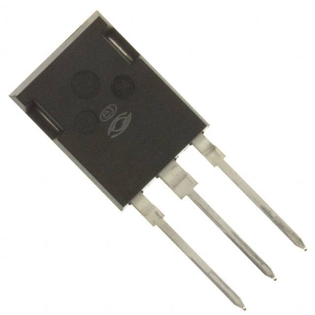
引脚分配:
- 引脚分配信息在文档中未明确列出,但通常TO-264封装的MOSFET有3个引脚:漏极(Drain)、栅极(Gate)和源极(Source)。
参数特性:
- 最大额定值包括漏极-源极电压(VDss)为500V,连续漏极电流(b)为58A,脉冲漏极电流(DM)为232A,栅极-源极电压(VGS)为+30V,瞬态栅极-源极电压(VGSM)为±40V,总功率耗散(P)为730W。
- 工作和存储结温范围(T TSTG)为-55到150°C。
功能详解:
- 静态电气特性包括漏极-源极击穿电压(BVpss),导通状态漏极电流(D(ON)),导通状态漏极-源极电阻(RDs(ON))等。
- 动态特性包括输入电容(Ciss)、输出电容(Coss)、反向传输电容(Crss)、导通延迟时间(t(on))、上升时间(t)、关闭延迟时间(t(off))和下降时间(t)。
- 热特性包括结到外壳的热阻(ReJC)和结到环境的热阻(ReJA)。
应用信息:
- 文档中未提供具体的应用案例,但线性MOSFET通常用于需要高电压和高电流的应用,如电源转换器、电机驱动器等。
封装信息:
- 提供了T-MAX™(B2)和TO-264(L)封装的外形图,包括尺寸和引脚布局。
注意事项:
- 这些器件对静电放电敏感,应遵循适当的处理程序。
其他信息:
- 文档还提供了最大有效瞬态热阻抗、结到外壳的热阻抗模型、典型性能曲线和最大安全工作区图。