APL602B2(G)
APL602L(G)
*G Denotes RoHS Compliant, Pb Free Terminal Finish.
600V 49A 0.125Ω
B2
LINEAR MOSFET
T-MAX™
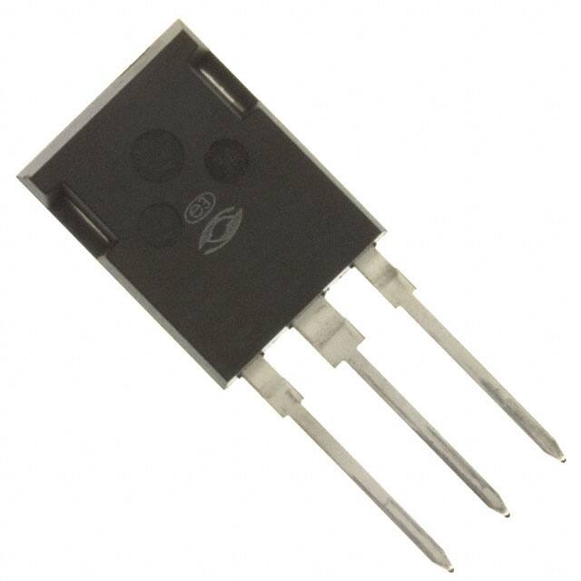
TO-264
Linear Mosfets are optimized for applications operating in the Linear
region where concurrent high voltage and high current can occur at
near DC conditions (>100 msec).
L
D
• Higher FBSOA
• Popular T-MAX™ or TO-264 Package
• Higher Power Dissipation
G
S
MAXIMUM RATINGS
Symbol
VDSS
ID
All Ratings: TC = 25°C unless otherwise specified.
APL602B2-L(G)
Parameter
600
Drain-Source Voltage
Volts
49
Continuous Drain Current @ TC = 25°C
1
UNIT
Amps
IDM
Pulsed Drain Current
VGS
Gate-Source Voltage Continuous
±30
VGSM
Gate-Source Voltage Transient
±40
Total Power Dissipation @ TC = 25°C
730
Watts
Linear Derating Factor
5.84
W/°C
PD
TJ,TSTG
196
Lead Temperature: 0.063" from Case for 10 Sec.
IAR
Avalanche Current
EAR
EAS
-55 to 150
Operating and Storage Junction Temperature Range
TL
1
49
1
Single Pulse Avalanche Energy
°C
300
(Repetitive and Non-Repetitive)
Repetitive Avalanche Energy
Volts
Amps
50
4
mJ
3000
STATIC ELECTRICAL CHARACTERISTICS
Characteristic / Test Conditions / Part Number
MIN
BVDSS
Drain-Source Breakdown Voltage (VGS = 0V, ID = 250 µA)
600
Volts
ID(ON)
On State Drain Current
49
Amps
IDSS
IGSS
VGS(TH)
(VDS > ID(ON) x R DS(ON) Max, VGS = 12V)
Drain-Source On-State Resistance
2
MAX
0.125
(VGS = 12V, 24.5A)
Zero Gate Voltage Drain Current (VDS = 600v, VGS = 0V)
25
Zero Gate Voltage Drain Current (VDS = 480V, VGS = 0V, TC = 125°C)
250
(VDS = VGS, ID = 2.5mA)
±100
nA
4
Volts
2
CAUTION: These Devices are Sensitive to Electrostatic Discharge. Proper Handling Procedures Should Be Followed.
APT Website - http://www.advancedpower.com
Ohms
µA
Gate-Source Leakage Current (VGS = ±30V, VDS = 0V)
Gate Threshold Voltage
UNIT
8-2003
RDS(ON)
2
TYP
050-5894 Rev E
Symbol
�APL602B2-L(G)
DYNAMIC CHARACTERISTICS
Symbol
Test Conditions
Characteristic
MIN
TYP
MAX
Ciss
Input Capacitance
VGS = 0V
7485
9000
Coss
Output Capacitance
VDS = 25V
1290
1810
Reverse Transfer Capacitance
f = 1 MHz
617
930
Turn-on Delay Time
VGS = 15V
13
26
Crss
td(on)
tr
td(off)
tf
Rise Time
Turn-off Delay Time
Fall Time
VDD = 300V
27
54
ID = 49A @ 25°C
56
84
RG = 0.6Ω
16
20
TYP
MAX
UNIT
pF
ns
THERMAL CHARACTERISTICS
Symbol Characteristic
MIN
RθJC
Junction to Case
.17
RθJA
Junction to Ambient
40
1 Repetitive Rating: Pulse width limited by maximum junction
temperature.
2 Pulse Test: Pulse width < 380 µS, Duty Cycle < 2%
3 See MIL-STD-750 Method 3471
4 Starting T = +25°C, L = 2.50mH, R = 25Ω, Peak I = 49A
j
G
L
APT Reserves the right to change, without notice, the specifications and information contained herein.
0.18
0.9
0.14
0.7
0.12
0.10
0.5
Note:
0.08
0.06
PDM
ZΘJC, THERMAL IMPEDANCE (°C/W)
0.16
0.3
t2
0.04
Duty Factor D = t1/t2
Peak TJ = PDM x ZθJC + TC
0.1
0.02
SINGLE PULSE
0.05
0
10-5
10-4
10-3
10-2
10-1
RECTANGULAR PULSE DURATION (SECONDS)
FIGURE 1, MAXIMUM EFFECTIVE TRANSIENT THERMAL IMPEDANCE, JUNCTION-TO-CASE vs PULSE DURATION
RC MODEL
Junction
temp. ( ”C)
0.0575
0.0187F
0.113
0.358F
8-2003
Power
(Watts)
050-5894 Rev E
t1
Case temperature
FIGURE 1a, TRANSIENT THERMAL IMPEDANCE MODEL
1.0
UNIT
°C/W
�APL602B2-L
APL602B2-L(G)
Typical Performance Curves
120
120
VGS=10V, 15 V
8V
80
7.5 V
60
7V
40
6.5 V
6V
20
100
8V
80
7.5 V
60
7V
40
6.5 V
6V
20
5.5 V
5.5 V
0
0
60
40
TJ = +125°C
20
TJ = -55°C
TJ = +25°C
0
0
2
4
6
8
10
VGS, GATE-TO-SOURCE VOLTAGE (VOLTS)
FIGURE 4, TRANSFER CHARACTERISTICS
ID, DRAIN CURRENT (AMPERES)
50
40
30
20
10
0
25
50
75
100
125
150
TC, CASE TEMPERATURE (°C)
FIGURE 6, MAXIMUM DRAIN CURRENT vs CASE TEMPERATURE
1.30
1.15
NORMALIZED TO
= 10V @ 29A
V
GS
1.20
VGS=10V
1.10
1.00
0.90
VGS=20V
0.80
0.70
0
20
40
60
80
100
120
ID, DRAIN CURRENT (AMPERES)
FIGURE 5, RDS(ON) vs DRAIN CURRENT
1.10
1.05
1.00
0.95
0.90
-50
0
50
100
150
TJ, JUNCTION TEMPERATURE (°C)
FIGURE 7, BREAKDOWN VOLTAGE vs TEMPERATURE
8-2003
VDS> ID (ON) x RDS (ON)MAX.
250µSEC. PULSE TEST
@
很抱歉,暂时无法提供与“APL602B2G”相匹配的价格&库存,您可以联系我们找货
免费人工找货