APT25GR120B_S
APT25GR120B
APT25GR120S
1200V, 25A, Vce(on) = 2.5V Typical
Ultra Fast NPT - IGBT®
(B)
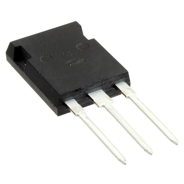
TO
The Ultra Fast NPT - IGBT® family of products is the newest generation of planar
IGBTs optimized for outstanding ruggedness and the best trade-off between
conduction and switching losses.
-2
D 3 PA K
47
(S)
C
G
Features
G
• Low Saturation Voltage
• Short Circuit Withstand Rated
• Low Tail Current
• High Frequency Switching
• RoHS Compliant
• Ultra Low Leakage Current
C
E
E
Unless stated otherwise, Microsemi discrete IGBTs contain a single IGBT die. This device is recommended for
applications such as induction heating (IH), motor control, general purpose inverters and uninterruptible power
supplies (UPS).
All Ratings: TC = 25°C unless otherwise specified.
MAXIMUM RATINGS
Symbol
Parameter
Ratings
Vces
Collector Emitter Voltage
1200
VGE
Gate-Emitter Voltage
±30
I C1
Continuous Collector Current @ TC = 25°C
75
I C2
Continuous Collector Current @ TC = 125°C
25
I CM
Pulsed Collector Current
100
SCWT
PD
TJ,TSTG
TL
1
Unit
V
A
Short Circuit Withstand Time: VCE = 600V, VGE = 15V, TC=125°C
10
μs
Total Power Dissipation @ TC = 25°C
521
W
Operating and Storage Junction Temperature Range
-55 to 150
Max. Lead Temp. for Soldering: 0.063" from Case for 10 Sec.
°C
300
STATIC ELECTRICAL CHARACTERISTICS
Symbol
Parameter
Min
V(BR)CES
Collector-Emitter Breakdown Voltage (VGE = 0V, I C = 500μA)
1200
VGE(TH)
Gate Threshold Voltage
VCE(ON)
I CES
Typ
Max
5.0
6.5
Collector-Emitter On Voltage (VGE = 15V, I C = 25A, Tj = 25°C)
2.5
3.2
Collector-Emitter On Voltage (VGE = 15V, I C = 25A, Tj = 125°C)
3.3
Collector-Emitter On Voltage (VGE = 15V, I C = 50A, Tj = 25°C)
3.5
(VCE = VGE, I C = 1.0mA, Tj = 25°C)
Collector Cut-off Current (VCE = 1200V, VGE = 0V, Tj = 25°C)
3.5
Collector Cut-off Current (VCE = 1200V, VGE = 0V, Tj = 125°C)
I GES
5
2
2
Unit
Volts
500
μA
±250
nA
50
Gate-Emitter Leakage Current (VGE = ±20V)
Microsemi Website - http://www.microsemi.com
052-6408
Rev A
1-2013
CAUTION: These Devices are Sensitive to Electrostatic Discharge. Proper Handling Procedures Should Be Followed.
�DYNAMIC CHARACTERISTICS
Symbol
Parameter
Test Conditions
Cies
Input Capacitance
Coes
Output Capacitance
Cres
Reverse Transfer Capacitance
VGEP
Gate to Emitter Plateau Voltage
Qg
Total Gate Charge
3
Gate-Emitter Charge
Qgc
Gate- Collector Charge
td(off)
tf
Capacitance
2784
VGE = 0V, VCE = 25V
271
Max
75
V
154
203
20
27
IC = 25A
76
97
VCE= 600V
Inductive Switching (25°C)
16
Current Rise Time
VCC = 600V
10
Turn-Off Delay Time
VGE = 15V
122
20
IC = 25A
Turn-On Switching Energy
RG = 4.3 Ω
742
1110
Turn-Off Switching Energy
TJ = +25°C
427
640
td(on)
Turn-On Delay Time
tr
td(off)
Eon2
4
Inductive Switching (125°C)
16
Current Rise Time
VCC = 600V
10
Turn-Off Delay Time
VGE = 15V
136
Current Fall Time
tf
nC
ns
Eoff 6
5
Unit
pF
7.5
Gate Charge
Current Fall Time
Eon2
Typ
f = 1MHz
Turn-On Delay Time
tr
Min
VGE = 15V
Qge
td(on)
APT25GR120B_S
μJ
ns
28
IC = 25A
5
Turn-On Switching Energy
RG = 4.3 Ω
Eoff 6
Turn-Off Switching Energy
TJ = +125°C
4
1297
1945
480
720
μJ
THERMAL AND MECHANICAL CHARACTERISTICS
Symbol
Characteristic
Min
Typ
Max
RθJC
Junction to Case Thermal Resistance
.24
RθJA
Junction to Ambient Thermal Resistance
40
WT
Package Weight
Torque
.22
Unit
°C/W
oz
6.2
g
Mounting Torque (TO-247 Package), 4-40 or M3 screw
10
in-lbf
6.2
N∙m
1 Repetitive Rating: Pulse width and case temperature limited by maximum junction temperature.
2 Pulse test: Pulse Width < 380μs, duty cycle < 2%.
3 See Mil-Std-750 Method 3471.
4 RG is external gate resistance, not including internal gate resistance or gate driver impedance. (MIC4452)
5 Eon2 is the clamped inductive turn on energy that includes a commutating diode reverse recovery current in the IGBT turn on energy loss. A combi device is used for the
clamping diode.
6 Eoff is the clamped inductive turn-off energy measured in accordance with JEDEC standard JESD24-1.
Microsemi reserves the right to change, without notice, the specifications and information contained herein.
052-6408
D = 0.9
0.20
0.7
0.15
0.5
Note:
0.10
P DM
ZθJC, THERMAL IMPEDANCE (°C/W)
Rev A
1-2013
0.25
0.3
t1
t2
0.05
t
0.1
0.05
SINGLE PULSE
Duty Factor D = 1 /t2
Peak T J = P DM x Z θJC + T C
0
10-5
10-4
10-2
10-3
0.1
RECTANGULAR PULSE DURATION (SECONDS)
Figure 1, Maximum Effective Transient Thermal Impedance, Junction-To-Case vs Pulse Duration
1
�TYPICAL PERFORMANCE CURVES
APT25GR120B_S
350
200
V
GE
= 15V
IC, COLLECTOR CURRENT (A)
300
200
150
100
50
30
40
50
IC(A)
FIGURE 2, Max Frequency vs Current (Tcase = 75°C)
180
15V
13V
160
IC, COLLECTOR CURRENT (A)
0
10
9V
120
8.5V
100
8.0V
80
7.5V
60
7V
40
6.5V
20
0
200
0
4
8
12
16
20
24
28
32
VCE, COLLECTOR-TO-EMITTER VOLTAGE (V)
FIGURE 4, Output Characteristics (TJ = 25°C)
IC, COLLECTOR CURRENT (A)
250μs PULSE
TEST
很抱歉,暂时无法提供与“APT25GR120B”相匹配的价格&库存,您可以联系我们找货
免费人工找货