APT26F120B2
APT26F120L
1200V, 27A, 0.58Ω Max, trr ≤335ns
N-Channel FREDFET
Power MOS 8™ is a high speed, high voltage N-channel switch-mode power MOSFET.
This 'FREDFET' version has a drain-source (body) diode that has been optimized for
high reliability in ZVS phase shifted bridge and other circuits through reduced trr, soft
recovery, and high recovery dv/dt capability. Low gate charge, high gain, and a greatly
reduced ratio of Crss/Ciss result in excellent noise immunity and low switching loss. The
intrinsic gate resistance and capacitance of the poly-silicon gate structure help control
di/dt during switching, resulting in low EMI and reliable paralleling, even when switching
at very high frequency.
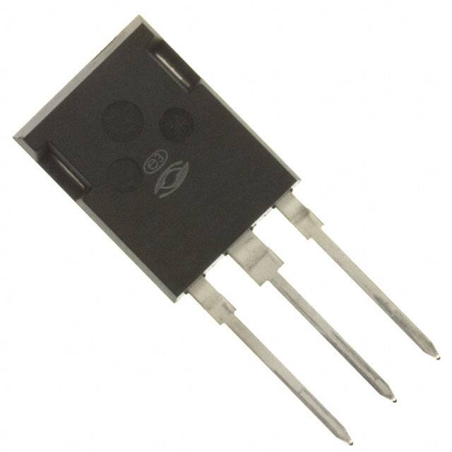
T-Max®
TO-264
APT26F120B2
APT26F120L
D
Single die FREDFET
G
S
TYPICAL APPLICATIONS
FEATURES
• Fast switching with low EMI
• ZVS phase shifted and other full bridge
• Low trr for high reliability
• Half bridge
• Ultra low Crss for improved noise immunity
• PFC and other boost converter
• Low gate charge
• Buck converter
• Avalanche energy rated
• Single and two switch forward
• RoHS compliant
• Flyback
Absolute Maximum Ratings
Symbol
ID
Parameter
Unit
Ratings
Continuous Drain Current @ TC = 25°C
27
Continuous Drain Current @ TC = 100°C
16
A
IDM
Pulsed Drain Current
VGS
Gate-Source Voltage
±30
V
EAS
Single Pulse Avalanche Energy 2
2165
mJ
IAR
Avalanche Current, Repetitive or Non-Repetitive
14
A
1
105
Thermal and Mechanical Characteristics
Min
Characteristic
Typ
Max
Unit
W
PD
Total Power Dissipation @ TC = 25°C
1135
RθJC
Junction to Case Thermal Resistance
0.11
RθCS
Case to Sink Thermal Resistance, Flat, Greased Surface
TJ,TSTG
°C/W
Operating and Storage Junction Temperature Range
-55
150
°C
TL
Soldering Temperature for 10 Seconds (1.6mm from case)
WT
Package Weight
Torque
0.11
300
0.22
oz
6.2
g
10
in·lbf
1.1
N·m
Mounting Torque ( TO-264 Package), 4-40 or M3 screw
Microsemi Website - http://www.microsemi.com
050-8143 Rev C 5-2009
Symbol
�Static Characteristics
TJ = 25°C unless otherwise specified
Symbol
Parameter
VBR(DSS)
Drain-Source Breakdown Voltage
ΔVBR(DSS)/ΔTJ
Breakdown Voltage Temperature Coefficient
RDS(on)
Drain-Source On Resistance
VGS(th)
Gate-Source Threshold Voltage
ΔVGS(th)/ΔTJ
Min
1200
VGS = 10V, ID = 14A
3
Zero Gate Voltage Drain Current
IGSS
Gate-Source Leakage Current
Dynamic Characteristics
VDS = 1200V
Forward Transconductance
Ciss
Input Capacitance
Crss
Reverse Transfer Capacitance
Coss
Output Capacitance
Typ
Max
1.41
0.48
4
-10
0.58
5
TJ = 25°C
VGS = 0V
250
1000
±100
TJ = 125°C
VGS = ±30V
Unit
V
V/°C
Ω
V
mV/°C
µA
nA
TJ = 25°C unless otherwise specified
Parameter
gfs
2.5
VGS = VDS, ID = 2.5mA
Threshold Voltage Temperature Coefficient
IDSS
Symbol
Test Conditions
VGS = 0V, ID = 250µA
Reference to 25°C, ID = 250µA
APT26F120B2_L
Min
Test Conditions
VDS = 50V, ID = 14A
4
Effective Output Capacitance, Charge Related
Co(er)
5
Effective Output Capacitance, Energy Related
Max
31
9670
115
715
VGS = 0V, VDS = 25V
f = 1MHz
Co(cr)
Typ
Unit
S
pF
275
VGS = 0V, VDS = 0V to 800V
Qg
Total Gate Charge
Qgs
Gate-Source Charge
Qgd
Gate-Drain Charge
td(on)
Turn-On Delay Time
tr
td(off)
tf
Current Rise Time
Turn-Off Delay Time
140
300
50
140
50
31
170
48
VGS = 0 to 10V, ID = 14A,
VDS = 600V
Resistive Switching
VDD = 800V, ID = 14A
RG = 2.2Ω 6 , VGG = 15V
Current Fall Time
nC
ns
Source-Drain Diode Characteristics
Symbol
IS
ISM
VSD
Parameter
Continuous Source Current
(Body Diode)
Pulsed Source Current
(Body Diode) 1
Diode Forward Voltage
trr
Reverse Recovery Time
Qrr
Reverse Recovery Charge
Irrm
Reverse Recovery Current
dv/dt
Peak Recovery dv/dt
Test Conditions
Min
Typ
D
MOSFET symbol
showing the
integral reverse p-n
junction diode
(body diode)
A
105
S
1.1
335
640
TJ = 25°C
TJ = 125°C
TJ = 25°C
VDD = 100V
TJ = 125°C
diSD/dt = 100A/µs
TJ = 25°C
Unit
27
G
ISD = 14A, TJ = 25°C, VGS = 0V
ISD = 14A 3
Max
TJ = 125°C
ISD ≤ 14A, di/dt ≤1000A/µs, VDD = 800V,
TJ = 125°C
1.72
4.67
11
16
V
ns
µC
A
25
V/ns
1 Repetitive Rating: Pulse width and case temperature limited by maximum junction temperature.
2 Starting at TJ = 25°C, L = 22.09mH, RG = 25Ω, IAS = 14A.
050-8143 Rev C 5-2009
3 Pulse test: Pulse Width < 380µs, duty cycle < 2%.
4 Co(cr) is defined as a fixed capacitance with the same stored charge as COSS with VDS = 67% of V(BR)DSS.
5 Co(er) is defined as a fixed capacitance with the same stored energy as COSS with VDS = 67% of V(BR)DSS. To calculate Co(er) for any value of
VDS less than V(BR)DSS, use this equation: Co(er) = -4.40E-7/VDS^2 + 5.34E-8/VDS + 7.59E-11.
6 RG is external gate resistance, not including internal gate resistance or gate driver impedance. (MIC4452)
Microsemi reserves the right to change, without notice, the specifications and information contained herein.
�APT26F120B2_L
70
25
V
GS
= 10V
T = 125°C
J
V
50
40
30
TJ = 25°C
20
10
0
15
5V
10
5
4.5V
TJ = 125°C
TJ = 150°C
0
0
5
10
15
20
25
30
VDS(ON), DRAIN-TO-SOURCE VOLTAGE (V)
0
Figure 2, Output Characteristics
NORMALIZED TO
VDS> ID(ON) x RDS(ON) MAX.
VGS = 10V @ 14A
250µSEC. PULSE TEST
@
很抱歉,暂时无法提供与“APT26F120B2”相匹配的价格&库存,您可以联系我们找货
免费人工找货- 国内价格 香港价格
- 30+227.4240030+29.43680