900V
36A
APT36N90BC3G*
*G Denotes RoHS Compliant, Pb Free Terminal Finish.
Super Junction MOSFET
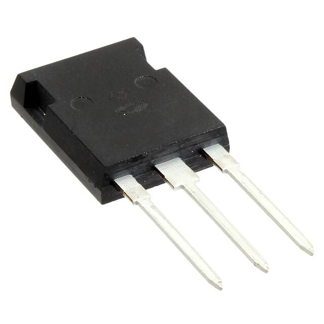
TO
-24
7
D3
• Ultra Low RDS(ON)
• Low Miller Capacitance
• Ultra Low Gate Charge, Qg
• Avalanche Energy Rated
D
• Extreme dv/dt Rated
• Dual die (parallel)
G
• Popular T-MAX Package
S
Unless stated otherwise, Microsemi discrete MOSFETs contain a single MOSFET die. This device is made with
two parallel MOSFET die. It is intended for switch-mode operation. It is not suitable for linear mode operation.
All Ratings per die: TC = 25°C unless otherwise specified.
MAXIMUM RATINGS
APT36N90BC3G
UNIT
Drain-Source Voltage
900
Volts
Continuous Drain Current @ TC = 25°C
36
Continuous Drain Current @ TC = 100°C
23
Symbol Parameter
VDSS
ID
Amps
IDM
Pulsed Drain Current
VGS
Gate-Source Voltage Continuous
±20
Volts
Total Power Dissipation @ TC = 25°C
390
Watts
PD
1
96
TJ,TSTG Operating and Storage Junction Temperature Range
TL
dv/
dt
Drain-Source Voltage slope (VDS = 400V, ID = 36A, TJ = 125°C)
50
V/ns
8.8
Amps
2
Avalanche Current
EAR
Repetitive Avalanche Energy
2
Single Pulse Avalanche Energy
°C
260
Lead Temperature: 0.063" from Case for 10 Sec.
IAR
EAS
-55 to 150
2.9
( Id = 8.8A, Vdd = 50V )
( Id = 8.8A, Vdd = 50V )
mJ
1940
STATIC ELECTRICAL CHARACTERISTICS
Characteristic / Test Conditions
BV(DSS)
Drain-Source Breakdown Voltage (VGS = 0V, ID = 250μA)
RDS(on)
IDSS
IGSS
VGS(th)
Drain-Source On-State Resistance
MIN
3
TYP
MAX
Volts
900
(VGS = 10V, ID = 18A)
UNIT
0.10
0.12
Ohms
Zero Gate Voltage Drain Current (VDS = 900V, VGS = 0V)
-
-
100
Zero Gate Voltage Drain Current (VDS = 900V, VGS = 0V, TC = 150°C)
-
50
-
Gate-Source Leakage Current (VGS = ±20V, VDS = 0V)
-
-
100
nA
2.5
3
3.5
Volts
Gate Threshold Voltage (VDS = VGS, ID = 2.9mA)
CAUTION: These Devices are Sensitive to Electrostatic Discharge. Proper Handling Procedures Should Be Followed.
"COOLMOS™ comprise a new family of transistors developed by Infineon Technologies AG. "COOLMOS" is a trademark of Infineon Technologies AG."
Microsemi Website - http://www.microsemi.com
μA
050-8068 Rev C 3-2012
Symbol
�APT36N90BC3G
Symbol
Characteristic
Input Capacitance
Coss
VGS = 0V
Output Capacitance
VDS = 25V
Reverse Transfer Capacitance
f = 1 MHz
Crss
Qg
Qgs
4
VGS = 10V
Gate-Source Charge
VDD = 450V
Total Gate Charge
Qgd
Gate-Drain ("Miller ") Charge
td(on)
Turn-on Delay Time
tr
td(off)
tf
MIN
Test Conditions
Ciss
TYP
7463
6827
INDUCTIVE SWITCHING
VGS = 15V
VDD = 600V
Turn-off Delay Time
ID = 36A @ 25°C
Eon
Turn-on Switching Energy
Eoff
Turn-off Switching Energy
Eon
Turn-on Switching Energy
Eoff
Turn-off Switching Energy
nC
ns
RG = 4.3Ω
25
5
INDUCTIVE SWITCHING @ 25°C
VDD = 600V, VGS = 15V
1500
ID = 36A, RG = 4.3Ω
750
5
INDUCTIVE SWITCHING @ 125°C
VDD = 600V, VGS = 15V
2130
Fall Time
UNIT
pF
167
252
38
112
70
20
400
ID = 36A @ 25°C
Rise Time
MAX
μJ
867
ID = 36A, RG = 4.3Ω
SOURCE-DRAIN DIODE RATINGS AND CHARACTERISTICS
Symbol
IS
Pulsed Source Current
1
VSD
Diode Forward Voltage
3
/dt
t rr
Q rr
IRRM
TYP
Continuous Source Current (Body Diode)
ISM
dv
MIN
Characteristic / Test Conditions
Peak Diode Recovery
dv
36
(Body Diode)
/dt
MAX
UNIT
Amps
96
(VGS = 0V, IS = 18A)
0.8
6
Reverse Recovery Time
(IS = -36A, di/dt = 100A/μs)
Reverse Recovery Charge
(IS = -36A, di/dt = 100A/μs)
Peak Recovery Current
(IS = -36A, di/dt = 100A/μs)
1.2
Volts
10
V/ns
Tj = 25°C
930
Tj = 125°C
1230
Tj = 25°C
35
μC
Tj = 125°C
Tj = 25°C
44
70
Tj = 125°C
Amps
68
ns
THERMAL CHARACTERISTICS
Symbol
Characteristic
MIN
TYP
MAX
RθJC
Junction to Case
0.3
RθJA
Junction to Ambient
31
1 Repetitive Rating: Pulse width limited by maximum junction
4 See MIL-STD-750 Method 3471
temperature
5 Eon includes diode reverse recovery.
2 Repetitive avalanche causes additional power losses that can
be calculated as PAV = EAR*f . Pulse width tp limited by Tj max. 6 Maximum 125°C diode commutation speed = di/dt 600A/μs
3 Pulse Test: Pulse width < 380 μs, Duty Cycle < 2%
Microsemi reserves the right to change, without notice, the specifications and information contained herein.
0.30
D = 0.9
0.25
0.7
0.20
0.5
Note:
0.10
0.3
P DM
ZθJC, THERMAL IMPEDANCE (°C/W)
050-8068 Rev C 3-2012
0.35
0.05
0.1
0.15
t1
t2
t
SINGLE PULSE
0.05
0
10
-5
Duty Factor D = 1 /t2
Peak T J = P DM x Z θJC + T C
10-2
0.1
10-3
RECTANGULAR PULSE DURATION (SECONDS)
Figure 1, Maximum Effective Transient Thermal Impedance, Junction-To-Case vs Pulse Duration
10
-4
10
UNIT
°C/W
�APT36N90BC3G
Typical Performance Curves
120
100
10 &15V
80
ID, DRAIN CURRENT (A)
IC, DRAIN CURRENT (A)
100
5.5V
80
60
5V
40
4.5V
20
70
60
50
40
30
0
5
10
15
20
25
30
VDS, DRAIN-TO-SOURCE VOLTAGE (V)
FIGURE 2, Low Voltage Output Characteristics
GS
0
1
2
3
4
5
6
40
= 10V @ 47A
35
ID, DRAIN CURRENT (A)
1.3
1.2
IDR, REVERSE
TJ= 125°C
VGS, GATE-TO-SOURCE VOLTAGE (V)
FIGURE 3, Transfer Characteristics
NORMALIZED TO
V
TJ= 25°C
10
0
1.4
TJ= -55°C
20
4V
0
VDS> ID (ON) x RDS (ON)MAX.
250μSEC. PULSE TEST
@
很抱歉,暂时无法提供与“APT36GA60BD15”相匹配的价格&库存,您可以联系我们找货
免费人工找货