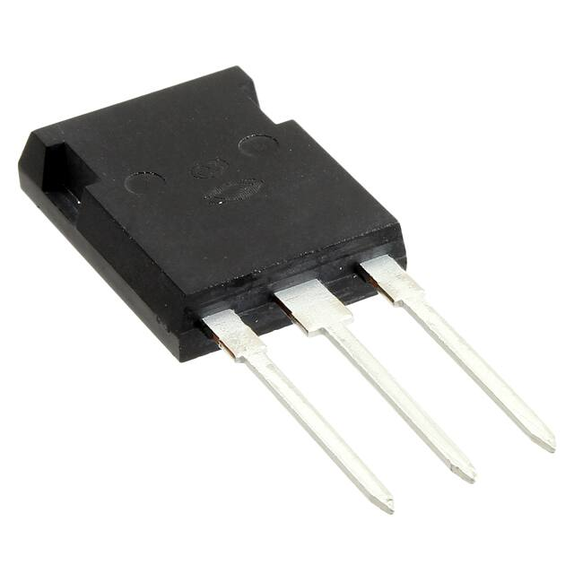
APT40GT60BR
600V, 80A, VCE(ON) = 2.1V Typical
Thunderbolt IGBT®
The Thunderbolt IGBT® is a new generation of high voltage power IGBTs. Using
Non-Punch-Through Technology, the Thunderbolt IGBT® offers superior ruggedness and ultrafast switching speed.
TO
-24
7
Features
• Low Forward Voltage Drop
• RBSOA and SCSOA Rated
• Low Tail Current
• High Frequency Switching to 150KHz
• RoHS Compliant
• Ultra Low Leakage Current
G
C
E
C
G
E
All Ratings: TC = 25°C unless otherwise specified.
Maximum Ratings
Symbol Parameter
Ratings
VCES
Collector-Emitter Voltage
600
VGE
Gate-Emitter Voltage
±20
IC1
Continuous Collector Current @ TC = 25°C
80
IC2
Continuous Collector Current @ TC = 105°C
40
ICM
Pulsed Collector Current 1
160
SSOA
PD
TJ, TSTG
Unit
Volts
Switching Safe Operating Area @ TJ = 150°C
Amps
160A @ 600V
Total Power Dissipation
Operating and Storage Junction Temperature Range
345
Watts
-55 to 150
°C
Static Electrical Characteristics
Min
Typ
Max
V(BR)CES
Collector-Emitter Breakdown Voltage (VGE = 0V, IC = 5mA)
600
-
-
VGE(TH)
Gate Threshold Voltage (VCE = VGE, IC = 500μA, Tj = 25°C)
3
4
5
Collector Emitter On Voltage (VGE = 15V, IC = 40A, Tj = 25°C)
1.6
2.15
2.5
Collector Emitter On Voltage (VGE = 15V, IC = 40A, Tj = 125°C)
-
-
2.8
Collector Cut-off Current (VCE = 600V, VGE = 0V, Tj = 25°C) 2
-
-
80
Collector Cut-off Current (VCE = 600V, VGE = 0V, Tj = 125°C) 2
-
-
2000
Gate-Emitter Leakage Current (VGE = ±20V)
-
-
100
VCE(ON)
ICES
IGES
Volts
μA
CAUTION: These Devices are Sensitive to Electrostatic Discharge. Proper Handling Procedures Should Be Followed.
Microsemi Website - http://www.microsemi.com
Unit
nA
052-6222 Rev D 3 - 2012
Symbol Characteristic / Test Conditions
�Dynamic Characteristic
Symbol
APT40GT60BR
Characteristic
Test Conditions
Cies
Input Capacitance
Coes
Output Capacitance
Cres
Reverse Transfer Capacitance
VGEP
Gate-to-Emitter Plateau Voltage
Qg
Total Gate Charge
Qge
Gate-Emitter Charge
Qgc
SSOA
td(on)
tr
td(off)
tf
Min
Typ
Max
-
2190
-
-
220
-
-
130
-
-
8.0
-
VGE = 15V
-
200
-
VCE= 300V
-
12
-
IC = 40A
-
86
-
TJ = 150°C, RG = 5Ω , VGE = 15V, L
160
VGE = 0V, VCE = 25V
3
f = 1MHz
Gate Charge
Gate-Collector Charge
Switching Safe Operating Area
= 100μH, VCE= 600V
Current Rise Time
Turn-Off Delay Time
12
-
Inductive Switching (25°C)
-
36
-
VCC = 400V
-
124
-
-
55
-
RG = 5Ω
-
-
-
TJ = +25°C
-
945
-
VGE = 15V
Current Fall Time
IC = 40A
Eon1
Turn-On Switching Energy
4
Eon2
Turn-On Switching Energy
5
Eoff
Turn-Off Switching Energy 6
-
828
-
td(on)
Turn-On Delay Time
-
12
-
Inductive Switching (125°C)
-
33
-
Turn-Off Delay Time
VCC = 400V
-
165
-
Current Fall Time
VGE = 15V
-
58
-
Turn-On Switching Energy
4
IC = 40A
-
-
Eon2
Turn-On Switching Energy
RG = 5Ω
-
5
-
1342
-
Eoff
Turn-Off Switching Energy 6
-
1150
-
tr
td(off)
tf
Eon1
Current Rise Time
TJ = +125°C
pF
V
nC
A
-
Turn-On Delay Time
Unit
ns
μJ
ns
μJ
Thermal and Mechanical Characteristics
Symbol Characteristic / Test Conditions
Min
Typ
Max
Unit
RθJC
Junction to Case (IGBT)
-
-
0.36
RθJC
Junction to Case (DIODE)
-
-
N/A
WT
Package Weight
-
6.1
-
g
-
-
10
in·lbf
-
-
1.1
N·m
2500
-
-
Volts
°C/W
Torque
Terminals and Mounting Screws
VIsolation
RMS Voltage (50-60Hz Sinusoidal Waveform from Terminals to Mounting Base for 1 Min.)
052-6222 Rev D 3 - 2012
1 Repetitive Rating: Pulse width limited by maximum junction temperature.
2 For Combi devices, Ices includes both IGBT and FRED leakages.
3 See MIL-STD-750 Method 3471.
4 Eon1 is the clamped inductive turn-on energy of the IGBT only, without the effect of a commutating diode reverse recovery current adding to
z a the IGBT turn-on loss. Tested in inductive switching test circuit shown in figure 21, but with a Silicon Carbide diode.
5 Eon2 is the clamped inductive turn-on energy that includes a commutating diode reverse recovery current in the IGBT turn-on switching
loss. (See Figures 21, 22.)
6 Eoff is the clamped inductive turn-off energy measured in accordance with JEDEC standard JESD24-1. (See Figures 21, 23.)
7 RG is external gate resistance not including gate driver impedance.
Microsemi reserves the right to change, without notice, the specifications and information contained herein.
�Typical Performance Curves
GE
15V
= 15V
TJ= 125°C
TJ= 25°C
TJ= 55°C
VCE, COLLECTOR-TO-EMITTER VOLTAGE (V)
FIGURE 1, Output Characteristics (TJ = 25°C)
TJ= 25°C
TJ= 125°C
TJ= -55°C
IC = 40A
IC = 200A
VCE, COLLECTOR-TO-EMITTER VOLTAGE (V)
VCE, COLLECTOR-TO-EMITTER VOLTAGE (V)
IC = 80A
10V
9V
8V
7V
6V
I = 40A
C
T = 25°C
J
VCE = 120V
VCE = 300V
VCE = 480V
GATE CHARGE (nC)
FIGURE 4, Gate charge
VGE, GATE-TO-EMITTER VOLTAGE (V)
FIGURE 3, Transfer Characteristics
TJ = 25°C.
250μs PULSE TEST
很抱歉,暂时无法提供与“APT40GT60BRG”相匹配的价格&库存,您可以联系我们找货
免费人工找货- 国内价格 香港价格
- 1+94.345831+12.10175
- 10+65.1089610+8.35154
- 25+57.3861925+7.36094
- 100+54.29568100+6.96452
