APT50N60JCCU2
ISOTOP® Boost chopper
VDSS = 600V
RDSon = 45mΩ max @ Tj = 25°C
ID = 50A @ Tc = 25°C
Super Junction
MOSFET Power Module
Application
• AC and DC motor control
• Switched Mode Power Supplies
• Power Factor Correction
• Brake switch
K
D
Features
•
G
-
S
D
ID
IDM
VGS
RDSon
PD
IAR
EAR
EAS
•
•
•
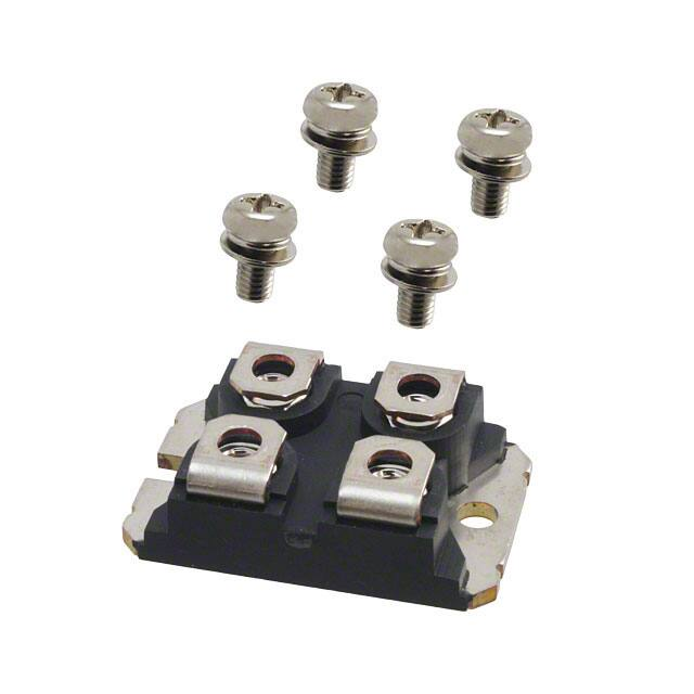
ISOTOP® Package (SOT-227)
Very low stray inductance
High level of integration
Benefits
• Outstanding performance at high frequency operation
• Stable temperature behavior
• Very rugged
• Direct mounting to heatsink (isolated package)
• Low junction to case thermal resistance
• Easy paralleling due to positive TC of VCEsat
• RoHS Compliant
Absolute maximum ratings
Symbol
VDSS
SiC Schottky Diode
- Zero reverse recovery
- Zero forward recovery
- Temperature Independent switching behavior
- Positive temperature coefficient on VF
Parameter
Drain - Source Breakdown Voltage
Tc = 25°C
Tc = 80°C
Continuous Drain Current
Pulsed Drain current
Gate - Source Voltage
Drain - Source ON Resistance
Maximum Power Dissipation
Avalanche current (repetitive and non repetitive)
Repetitive Avalanche Energy
Single Pulse Avalanche Energy
Tc = 25°C
Max ratings
600
50
38
130
±20
45
290
15
3
1900
Unit
V
A
V
mΩ
W
A
mJ
These Devices are sensitive to Electrostatic Discharge. Proper Handing Procedures Should Be Followed.
www.microsemi.com
1-4
APT50N60JCCU2 – Rev 3 October, 2012
G
•
K
S
Ultra low RDSon
Low Miller capacitance
Ultra low gate charge
Avalanche energy rated
�APT50N60JCCU2
All ratings @ Tj = 25°C unless otherwise specified
Electrical Characteristics
Symbol Characteristic
IDSS
RDS(on)
VGS(th)
IGSS
Test Conditions
Min
Zero Gate Voltage Drain Current
VGS = 0V,VDS = 600V
Drain – Source on Resistance
Gate Threshold Voltage
Gate – Source Leakage Current
Typ
Tj = 25°C
Tj = 125°C
VGS = 0V,VDS = 600V
VGS = 10V, ID = 22.5A
VGS = VDS, ID = 3mA
VGS = ±20 V, VDS = 0V
2.1
40
3
Max
250
500
45
3.9
100
Unit
Max
Unit
µA
mΩ
V
nA
Dynamic Characteristics
Symbol Characteristic
Ciss
Input Capacitance
Coss
Output Capacitance
Qg
Total gate Charge
Qgs
Gate – Source Charge
Qgd
Gate – Drain Charge
Td(on)
Turn-on Delay Time
Tr
Td(off)
Tf
Test Conditions
VGS = 0V ; VDS = 25V
f = 1MHz
Fall Time
Turn-on Switching Energy
Eoff
Turn-off Switching Energy
Eon
Turn-on Switching Energy
Eoff
Turn-off Switching Energy
VSD
Diode Forward Voltage
trr
Reverse Recovery Time
Qrr
Reverse Recovery Charge
nF
34
nC
51
30
Tj=25°C
VGS = 10V
VBus = 400V
ID = 44A
RG = 3.3Ω
Turn-off Delay Time
Typ
6.8
0.32
150
VGS = 10V
VBus = 300V
ID = 44A
Rise Time
Eon
Min
20
ns
100
20
Tj=25°C
VGS = 10V ; VBus = 400V
ID = 44A ; RG = 3.3Ω
Tj=125°C
VGS = 10V ; VBus = 400V
ID = 44A ; RG = 3.3Ω
405
µJ
520
660
µJ
635
VGS = 0V, IS = - 44A
IS = - 44A
Tj = 25°C
VR = 400V
Tj = 25°C
diS/dt = 100A/µs
0.9
1.2
V
600
ns
17
µC
SiC chopper diode ratings and characteristics
Test Conditions
IRM
Maximum Reverse Leakage Current
VR=600V
IF(AV)
Maximum Average Forward Current
50% duty cycle
Min
600
Tj = 25°C
Tj = 175°C
Tc = 125°C
Tj = 25°C
Tj = 175°C
Typ
Max
100
200
20
1.6
2
400
2000
VF
Diode Forward Voltage
IF = 20A
QC
Total Capacitive Charge
IF = 20A, VR = 300V
di/dt =800A/µs
28
Q
Total Capacitance
f = 1MHz, VR = 200V
130
f = 1MHz, VR = 400V
100
www.microsemi.com
Unit
V
µA
A
1.8
2.4
V
nC
pF
2-4
APT50N60JCCU2 – Rev 3 October, 2012
Symbol Characteristic
VRRM Maximum Peak Repetitive Reverse Voltage
�APT50N60JCCU2
Thermal and package characteristics
Symbol Characteristic
Min
RthJC
Junction to Case Thermal Resistance
RthJA
VISOL
TJ,TSTG
TL
Torque
Wt
Junction to Ambient (IGBT & Diode)
Typ
CoolMos
SiC Diode
RMS Isolation Voltage, any terminal to case t =1 min, I isol
很抱歉,暂时无法提供与“APT50N60JCCU2”相匹配的价格&库存,您可以联系我们找货
免费人工找货