APT51F50J
500V, 51A, 0.075Ω Max, trr ≤310ns
N-Channel FREDFET
S
S
Power MOS 8™ is a high speed, high voltage N-channel switch-mode power MOSFET.
This 'FREDFET' version has a drain-source (body) diode that has been optimized for
high reliability in ZVS phase shifted bridge and other circuits through reduced trr, soft
recovery, and high recovery dv/dt capability. Low gate charge, high gain, and a greatly
reduced ratio of Crss/Ciss result in excellent noise immunity and low switching loss. The
intrinsic gate resistance and capacitance of the poly-silicon gate structure help control
di/dt during switching, resulting in low EMI and reliable paralleling, even when switching
at very high frequency.
D
G
SO
2
T-
27
"UL Recognized"
file # E145592
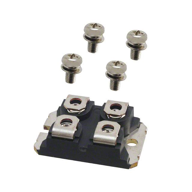
ISOTOP ®
D
APT51F50J
Single die FREDFET
G
S
FEATURES
TYPICAL APPLICATIONS
• Fast switching with low EMI
• ZVS phase shifted and other full bridge
• Low trr for high reliability
• Half bridge
• Ultra low Crss for improved noise immunity
• PFC and other boost converter
• Low gate charge
• Buck converter
• Avalanche energy rated
• Single and two switch forward
• RoHS compliant
• Flyback
Absolute Maximum Ratings
Symbol
ID
Parameter
Ratings
Continuous Drain Current @ TC = 25°C
51
Continuous Drain Current @ TC = 100°C
32
230
Unit
A
IDM
Pulsed Drain Current
VGS
Gate-Source Voltage
±30
V
EAS
Single Pulse Avalanche Energy 2
1580
mJ
IAR
Avalanche Current, Repetitive or Non-Repetitive
37
A
1
Thermal and Mechanical Characteristics
Max
Unit
Total Power Dissipation @ TC = 25°C
480
W
RθJC
Junction to Case Thermal Resistance
0.26
RθCS
Case to Sink Thermal Resistance, Flat, Greased Surface
TJ,TSTG
Operating and Storage Junction Temperature Range
-55
VIsolation
RMS Voltage (50-60hHz Sinusoidal Waveform from Terminals to Mounting Base for 1 Min.)
2500
V
WT
Torque
Package Weight
Terminals and Mounting Screws.
MicrosemiWebsite-http://www.microsemi.com
Downloaded from Elcodis.com electronic components distributor
0.15
150
°C/W
°C
1.03
oz
29.2
g
10
in·lbf
1.1
N·m
01-2009
PD
Typ
Rev B
Min
050-8127
Characteristic
Symbol
�Static Characteristics
TJ = 25°C unless otherwise specified
APT51F50J
Symbol
Parameter
Test Conditions
Min
VBR(DSS)
Drain-Source Breakdown Voltage
VGS = 0V, ID = 250µA
500
∆VBR(DSS)/∆TJ
Drain-Source On Resistance
VGS(th)
Gate-Source Threshold Voltage
∆VGS(th)/∆TJ
VGS = VDS, ID = 2.5mA
Threshold Voltage Temperature Coefficient
Zero Gate Voltage Drain Current
IGSS
Gate-Source Leakage Current
Dynamic Characteristics
Forward Transconductance
VDS = 500V
TJ = 25°C
VGS = 0V
TJ = 125°C
VGS = ±30V
Min
Test Conditions
VDS = 50V, ID = 37A
Typ
Output Capacitance
55
11600
160
1250
725
365
290
65
130
45
55
120
39
Min
Typ
Ciss
Input Capacitance
Crss
Reverse Transfer Capacitance
Coss
Max
0.075
5
Unit
V
V/°C
Ω
V
mV/°C
250
1000
±100
µA
nA
TJ = 25°C unless otherwise specified
Parameter
gfs
0.60
0.064
2.5
4
-10
VGS = 10V, ID = 37A
3
IDSS
Symbol
Reference to 25°C, ID = 250µA
Breakdown Voltage Temperature Coefficient
RDS(on)
Typ
VGS = 0V, VDS = 25V
f = 1MHz
Co(cr)
4
Effective Output Capacitance, Charge Related
Co(er)
5
Effective Output Capacitance, Energy Related
Max
Unit
S
pF
VGS = 0V, VDS = 0V to 333V
Qg
Total Gate Charge
Qgs
Gate-Source Charge
Qgd
Gate-Drain Charge
td(on)
Turn-On Delay Time
tr
td(off)
tf
VGS = 0 to 10V, ID = 37A,
VDS = 250V
Resistive Switching
VDD = 333V, ID = 37A
Current Rise Time
RG = 2.2Ω 6 , VGG = 15V
Turn-Off Delay Time
Current Fall Time
nC
ns
Source-Drain Diode Characteristics
Symbol
IS
ISM
VSD
Continuous Source Current
(Body Diode)
(Body Diode) 1
Qrr
Reverse Recovery Charge
Irrm
Reverse Recovery Current
Peak Recovery dv/dt
TJ = 25°C
TJ = 125°C
TJ = 25°C
VDD = 100V
TJ = 125°C
diSD/dt = 100A/µs
TJ = 25°C
TJ = 125°C
ISD ≤ 37A, di/dt ≤1000A/µs, VDD =
Unit
51
A
ISD = 37A 3
S
Max
G
ISD = 37A, TJ = 25°C, VGS = 0V
Diode Forward Voltage
Reverse Recovery Time
D
MOSFET symbol
showing the
integral reverse p-n
junction diode
(body diode)
Pulsed Source Current
trr
dv/dt
Test Conditions
Parameter
333V,
TJ = 125°C
230
1.48
3.85
11.3
16.6
1.0
310
570
20
V
ns
µC
A
V/ns
1 Repetitive Rating: Pulse width and case temperature limited by maximum junction temperature.
050-8127
Rev B
01-2009
2 Starting at TJ = 25°C, L = 2.31mH, RG = 25Ω, IAS = 37A.
3 Pulse test: Pulse Width < 380µs, duty cycle < 2%.
4 Co(cr) is defined as a fixed capacitance with the same stored charge as COSS with VDS = 67% of V(BR)DSS.
5 Co(er) is defined as a fixed capacitance with the same stored energy as COSS with VDS = 67% of V(BR)DSS. To calculate Co(er) for any value of
VDS less than V(BR)DSS, use this equation: Co(er) = -1.65E-7/VDS^2 + 5.51E-8/VDS + 2.03E-10.
6 RG is external gate resistance, not including internal gate resistance or gate driver impedance. (MIC4452)
Microsemi reserves the right to change, without notice, the specifications and information contained herein.
Downloaded from Elcodis.com electronic components distributor
�300
V
GS
= 10V
T = 125°C
J
200
TJ = 25°C
150
100
TJ = 150°C
50
80
6V
60
5.5V
40
TJ = 125°C
0
0
5
10
15
20
25
VDS(ON), DRAIN-TO-SOURCE VOLTAGE (V)
2.5
5V
0
NORMALIZED TO
250µSEC. PULSE TEST
@ ID(ON) x RDS(ON) MAX.
VGS = 10V @ 37A
0
5
10
15
20
25
30
VDS, DRAIN-TO-SOURCE VOLTAGE (V)
Figure 2, Output Characteristics
250
TJ = -55°C
100
20
100
= 7 & 10V
050-8127
GS
6.5V
Figure 1, Output Characteristics
RDS(ON), DRAIN-TO-SOURCE ON RESISTANCE
ID, DRIAN CURRENT (A)
ID, DRAIN CURRENT (A)
TJ = -55°C
0
V
120
250
APT51F50J
140
�APT51F50J
300
300
13µs
100µs
1ms
10ms
100ms
DC line
1
1
Rds(on)
TJ (°C)
100ms
DC line
TJ = 150°C
TC = 25°C
1
0.1
10
100
800
VDS, DRAIN-TO-SOURCE VOLTAGE (V)
Figure 9, Forward Safe Operating Area
13µs
100µs
1ms
10ms
10
TJ = 125°C
TC = 75°C
IDM
Scaling for Different Case & Junction
Temperatures:
ID = ID(T = 25°C)*(TJ - TC)/125
C
1
10
100
800
VDS, DRAIN-TO-SOURCE VOLTAGE (V)
Figure 10, Maximum Forward Safe Operating Area
TC (°C)
0.0394
0.217
0.00348
ZEXT
Rds(on)
0.1
ID, DRAIN CURRENT (A)
10
100
IDM
ID, DRAIN CURRENT (A)
100
Dissipated Power
(Watts)
0.0255
0.422
153.3
ZEXT are the external thermal
impedances: Case to sink,
sink to ambient, etc. Set to
zero when modeling only
the case to junction.
Figure 11, Transient Thermal Impedance Model
0.25
D = 0.9
0.20
0.7
0.15
Note:
0.5
PDM
ZθJC, THERMAL IMPEDANCE (°C/W)
0.30
0.10
0.3
t1
t2
t1 = Pulse Duration
t
0.05
0
0.1
SINGLE PULSE
0.05
10
-5
Duty Factor D = 1/t2
Peak TJ = PDM x ZθJC + TC
10
10
10-2
10-1
RECTANGULAR PULSE DURATION (seconds)
Figure 12. Maximum Effective Transient Thermal Impedance Junction-to-Case vs Pulse Duration
-4
-3
1.0
SOT-227 (ISOTOP®) Package Outline
11.8 (.463)
12.2 (.480)
31.5 (1.240)
31.7 (1.248)
7.8 (.307)
8.2 (.322)
r = 4.0 (.157)
(2 places)
25.2 (0.992)
0.75 (.030) 12.6 (.496) 25.4 (1.000)
0.85 (.033) 12.8 (.504)
4.0 (.157)
4.2 (.165)
(2 places)
01-2009
Rev B
3.3 (.129)
3.6 (.143)
14.9 (.587)
15.1 (.594)
38.0 (1.496)
38.2 (1.504)
050-8127
W=4.1 (.161)
W=4.3 (.169)
H=4.8 (.187)
H=4.9 (.193)
(4 places)
8.9 (.350)
9.6 (.378)
Hex Nut M4
(4 places)
1.95 (.077)
2.14 (.084)
* Source
30.1 (1.185)
30.3 (1.193)
Drain
* Emitter terminals are shorted
internally. Current handling
capability is equal for either
Source terminal.
* Source
Gate
Dimensions in Millimeters and (Inches)
ISOTOP® is a registered trademark of ST Microelectronics NV. Microsemi's products are covered by one or more of U.S.patents 4,895,810 5,045,903 5,089,434 5,182,234
5,019,522 5,262,336 6,503,786 5,256,583 4,748,103 5,283,202 5,231,474 5,434,095 5,528,058 and foreign patents. US and Foreign patents pending. All Rights Reserved.
Downloaded from Elcodis.com electronic components distributor
�