APT60GT60JR
600V
Thunderbolt IGBT
93A
E
E
The Thunderbolt IGBT™ is a new generation of high voltage power IGBTs.
Using Non-Punch Through Technology the Thunderbolt IGBT™ offers superior
ruggedness and ultrafast switching speed.
27
2
T-
C
G
SO
"UL Recognized"
• Low Forward Voltage Drop
• High Freq. Switching to 150KHz
• Low Tail Current
• Ultra Low Leakage Current
• Avalanche Rated
• RBSOA and SCSOA Rated
ISOTOP ®
C
G
E
MAXIMUM RATINGS
Symbol
All Ratings: TC = 25°C unless otherwise specified.
Parameter
VCES
Collector-Emitter Voltage
600
VCGR
Collector-Gate Voltage (RGE = 20KΩ)
600
VGE
Gate Emitter Voltage
±20
I C1
Continuous Collector Current @ TC = 25°C
93
I C2
Continuous Collector Current @ TC = 95°C
60
I CM
Pulsed Collector Current
I LM
RBSOA Clamped Inductive Load Current RG = 11Ω TC = 25°C
EAS
Single Pule Avalanche Energy 2
PD
Total Power Dissipation
TJ,TSTG
TL
UNIT
APT60GT60JR
1
Volts
Amps
@ TC = 25°C
360
360
Operating and Storage Junction Temperature Range
65
mJ
378
Watts
-55 to 150
°C
300
Max. Lead Temp. for Soldering: 0.063" from Case for 10 Sec.
STATIC ELECTRICAL CHARACTERISTICS
BVCES
VGE(TH)
VCE(ON)
I CES
I GES
Characteristic / Test Conditions
MIN
Collector-Emitter Breakdown Voltage (VGE = 0V, I C = 0.5mA)
600
Gate Threshold Voltage
3
(VCE = VGE, I C = 500µA, Tj = 25°C)
Collector-Emitter On Voltage (VGE = 15V, I C = I C2, Tj = 25°C)
TYP
MAX
4
5
2.0
2.5
Collector-Emitter On Voltage (VGE = 15V, I C = I C2, Tj = 125°C)
2.8
Collector Cut-off Current (VCE = VCES, VGE = 0V, Tj = 25°C)
80
Collector Cut-off Current (VCE = VCES, VGE = 0V, Tj = 125°C)
2000
Gate-Emitter Leakage Current (VGE = ±20V, VCE = 0V)
±100
UNIT
Volts
µA
nA
CAUTION: These Devices are Sensitive to Electrostatic Discharge. Proper Handling Procedures Should Be Followed.
APT Website - http://www.advancedpower.com
USA
405 S.W. Columbia Street
Bend, Oregon 97702-1035
Phone: (541) 382-8028
FAX: (541) 388-0364
EUROPE
Chemin de Magret
F-33700 Merignac - France
Phone: (33) 5 57 92 15 15
FAX: (33) 5 56 47 97 61
052-6221 Rev D 6-2008
Symbol
�DYNAMIC CHARACTERISTICS
Symbol
Test Conditions
Characteristic
Cies
Input Capacitance
Coes
Output Capacitance
Cres
Reverse Transfer Capacitance
Total Gate Charge
Qge
Gate-Emitter Charge
Qgc
Gate-Collector ("Miller") Charge
tr
td(off)
tf
td(on)
tr
td(off)
tf
Turn-on Delay Time
MIN
Capacitance
VGE = 0V
pF
257
410
19
30
I C = I C2
120
180
Resistive Switching (25°C)
20
40
VGE = 15V
95
190
315
470
245
490
25
50
59
120
430
650
65
130
VCC = 0.5VCES
VCC = 0.5VCES
I C = I C2
RG = 5Ω
Fall Time
Turn-on Delay Time
Inductive Switching (150°C)
VCLAMP(Peak) = 0.66VCES
VGE = 15V
Fall Time
I C = I C2
Turn-on Switching Energy
R G = 5Ω
1.6
3.2
Eoff
Turn-off Switching Energy
TJ = +150°C
2.4
4.8
Ets
Total Switching Losses
4.0
8.0
26
50
63
125
395
590
R G = 5Ω
68
140
TJ = +25°C
3.4
7.0
Eon
td(on)
tr
td(off)
tf
Turn-on Delay Time
Rise Time
Inductive Switching (25°C)
VCLAMP(Peak) = 0.66VCES
Turn-off Delay Time
Fall Time
Ets
Total Switching Losses
gfe
Forward Transconductance
VGE = 15V
I C = I C2
VCE = 20V, I C = I C2
UNIT
92
Gate Charge
VGE = 15V
Turn-off Delay Time
Turn-off Delay Time
MAX
150
f = 1 MHz
Rise Time
Rise Time
TYP
1600
VCE = 25V
3
Qg
td(on)
APT60GT60JR
4
nC
ns
ns
mJ
ns
mJ
S
THERMAL AND MECHANICAL CHARACTERISTICS
Symbol
RΘJC
Junction to Case
RΘJA
Junction to Ambient
WT
Torque
052-6221 Rev D 6-2008
Characteristic
MIN
TYP
MAX
UNIT
0.33
°C/W
Package Weight
20
1.03
oz
29.2
gm
10
lb•in
1.5
N•m
Mounting Torque (Mounting = 8-32 or 4mm Machine and Terminals = 4mm Machine)
1
Repetitive Rating: Pulse width limited by maximum junction temperature.
2
IC = IC2, RGE = 25Ω, L = 100µH, Tj = 25°C
3
See MIL-STD-750 Method 3471
APT Reserves the right to change, without notice, the specifications and information contained herein.
�160
VGE=17, 15, 13, 11 & 10V
9V
120
8V
80
7V
40
6V
IC, COLLECTOR CURRENT (AMPERES)
IC, COLLECTOR CURRENT (AMPERES)
160
0
IC, COLLECTOR CURRENT (AMPERES)
IC, COLLECTOR CURRENT (AMPERES)
7V
40
6V
200
120
TC=+25°C
TC=+150°C
80
TC=-55°C
40
8V
80
5V
0
4
8
12
16
20
VCE, COLLECTOR-TO-EMITTER VOLTAGE (VOLTS)
Figure 2, Typical Output Characteristics (TJ = 150°C)
160
250 µsec. Pulse Test
VGE = 15V
9V
120
0
0
4
8
12
16
20
VCE, COLLECTOR-TO-EMITTER VOLTAGE (VOLTS)
Figure 1, Typical Output Characteristics (TJ = 25°C)
100
OPERATION
LIMITED
BY
VCE (SAT)
100µs
1ms
10
5
TC =+25°C
TJ =+150°C
SINGLE PULSE
10ms
1
0
10,000
Cies
1,000
f = 1MHz
Coes
Cres
100
0.01
0.1
1.0
10
50
VCE, COLLECTOR-TO-EMITTER VOLTAGE (VOLTS)
Figure 5, Typical Capacitance vs Collector-To-Emitter Voltage
1
5 10
50 100
600
VCE, COLLECTOR-TO-EMITTER VOLTAGE (VOLTS)
Figure 4, Maximum Forward Safe Operating Area
VGE, GATE-TO-EMITTER VOLTAGE (VOLTS)
0
1
2
3
4
5
VCE, COLLECTOR-TO-EMITTER VOLTAGE (VOLTS)
Figure 3, Typical Output Characteristics @ VGE = 15V
C, CAPACITANCE (pF)
VGE=17, 15, 13, 11 & 10V
20
IC = IC2
TJ = +25°C
VCE=120V
16
VCE=300V
12
VCE=480V
8
4
0
0
100
200
300
400
Qg, TOTAL GATE CHARGE (nC)
Figure 6, Gate Charges vs Gate-To-Emitter Voltage
D=0.5
0.1
0.2
0.05
0.1
0.05
Note:
0.02
0.01
0.005
SINGLE PULSE
t1
t2
Duty Factor D = t1/t2
Peak TJ = PDM x ZθJC + TC
0.001
10-5
10-4
10-3
10-2
10-1
1.0
RECTANGULAR PULSE DURATION (SECONDS)
Figure 7, Maximum Effective Transient Thermal Impedance, Junction-To-Case vs Pulse Duration
10
052-6221 Rev D 6-2008
0.01
PDM
ZθJC, THERMAL IMPEDANCE (°C/W)
0.35
�APT60GT60JR
100
3.5
IC, COLLECTOR CURRENT (AMPERES)
VCE(SAT), COLLECTOR-TO-EMITTER
SATURATION VOLTAGE (VOLTS)
4.0
IC1
3.0
2.5
IC2
2.0
0.5 IC2
1.5
1.0
-50
70
60
50
40
30
20
10
25
50
75
100
125
150
TC, CASE TEMPERATURE (°C)
Figure 9, Maximum Collector Current vs Case Temperature
8.0
SWITCHING ENERGY LOSSES (mJ)
BVCES, COLLECTOR-TO-EMITTER BREAKDOWN
VOLTAGE (NORMALIZED)
80
0
-25
0
25 50 75 100 125 150
TJ, JUNCTION TEMPERATURE (°C)
Figure 8, Typical VCE(SAT) Voltage vs Junction Temperature
1.2
1.1
1
0.9
0.8
0.7
VCC = 0.66 VCES
VGE = +15V
TJ = +25°C
IC = IC2
6.0
Eoff
4.0
Eon
2.0
0
-25
0
25 50 75 100 125 150
TJ, JUNCTION TEMPERATURE (°C)
Figure 10, Breakdown Voltage vs Junction Temperature
-50
0
20
40
60
80
100
RG, GATE RESISTANCE (OHMS)
Figure 11, Typical Switching Energy Losses vs Gate Resistance
2.5
20
SWITCHING ENERGY LOSSES (mJ)
TOTAL SWITCHING ENERGY LOSSES (mJ)
90
IC1
10
VCC = 0.66 VCES
VGE = +15V
RG = 10 Ω
IC2
0.5 IC2
1
-50
2.0
VCC = 0.66 VCES
VGE = +15V
TJ = +125°C
RG = 10 Ω
Eoff
1.5
1.0
Eon
0.5
0
-25
0
25 50 75 100 125 150
TJ, JUNCTION TEMPERATURE (°C)
Figure 12, Typical Switching Energy Losses vs. Junction Temperature
0
10
20
30
40
50
60
IC, COLLECTOR CURRENT (AMPERES)
Figure 13, Typical Switching Energy Losses vs Collector Current
IC, COLLECTOR CURRENT (AMPERES)
052-6221 Rev D 6-2008
120
For Both:
Duty Cycle = 50%
TJ = +125°C
Tsink = +90°C
Gate drive as specified
Power dissapation = 140W
ILOAD = IRMS of fundamental
10
1
0.1
1.0
10
F, FREQUENCY (KHz)
Figure 14,Typical Load Current vs Frequency
100
1000
�APT60GT60JR
VCHARGE
*DRIVER SAME TYPE AS D.U.T.
VCC = 0.66 VCES
Et s = E on + E off
A
A
90%
VC
B
10%
B
t d (on)
IC
t d(off)
IC
VC
100uH
90%
D.U.T.
VCE (SAT)
tr
VC
A
D.U.T.
DRIVER*
10%
IC
RG
V CLAMP
90%
10%
tf
E on
E off
t=2us
Figure 15, Switching Loss Test Circuit and Waveforms
2
VCE(off)
VGE(on)
V CC
90%
.5 VCES
RL =
I C2
2
D.U.T.
10%
VGE(off)
t d (on)
tr
t d(off)
1
tf
Figure 16, Resistive Switching Time Test Circuit and Waveforms
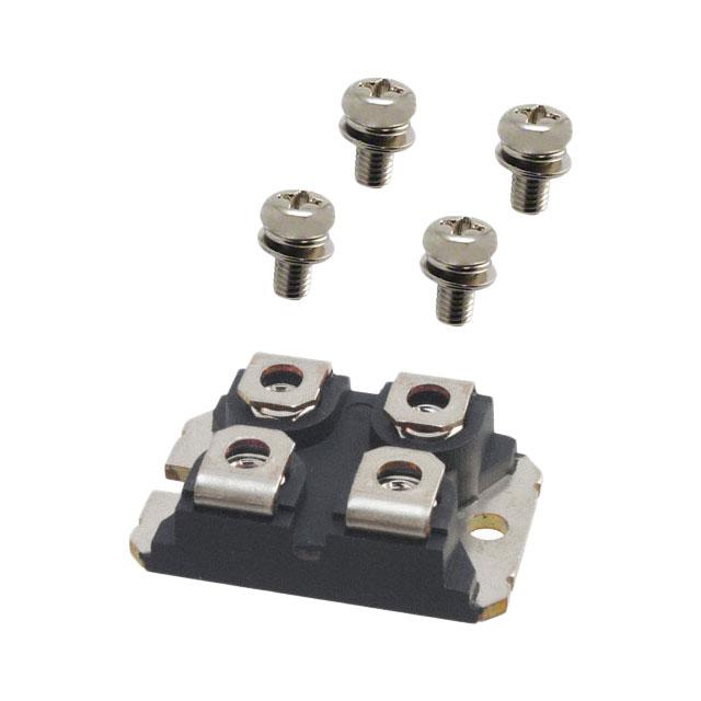
SOT-227 (ISOTOP®) Package Outline
11.8 (.463)
12.2 (.480)
31.5 (1.240)
31.7 (1.248)
7.8 (.307)
8.2 (.322)
r = 4.0 (.157)
(2 places)
W=4.1 (.161)
W=4.3 (.169)
H=4.8 (.187)
H=4.9 (.193)
(4 places)
8.9 (.350)
9.6 (.378)
Hex Nut M4
(4 places)
25.2 (0.992)
0.75 (.030) 12.6 (.496) 25.4 (1.000)
0.85 (.033) 12.8 (.504)
4.0 (.157)
4.2 (.165)
(2 places)
3.3 (.129)
3.6 (.143)
14.9 (.587)
15.1 (.594)
1.95 (.077)
2.14 (.084)
* Emitter
30.1 (1.185)
30.3 (1.193)
Collector
* Emitter terminals are shorted
internally. Current handling
capability is equal for either
Source terminal.
38.0 (1.496)
38.2 (1.504)
* Emitter
Dimensions in Millimeters and (Inches)
Gate
052-6221 Rev D 6-2008
1
From
Gate Drive
Circuitry
VCE(on)
RG
�