APT8052BLL
APT8052SLL
800V 15A
POWER MOS 7
R
MOSFET
BLL
D3PAK
®
Power MOS 7 is a new generation of low loss, high voltage, N-Channel
enhancement mode power MOSFETS. Both conduction and switching
®
losses are addressed with Power MOS 7 by significantly lowering RDS(ON)
®
and Qg. Power MOS 7 combines lower conduction and switching losses
along with exceptionally fast switching speeds inherent with APT's
patented metal gate structure.
• Lower Input Capacitance
• Lower Miller Capacitance
• Lower Gate Charge, Qg
VDSS
ID
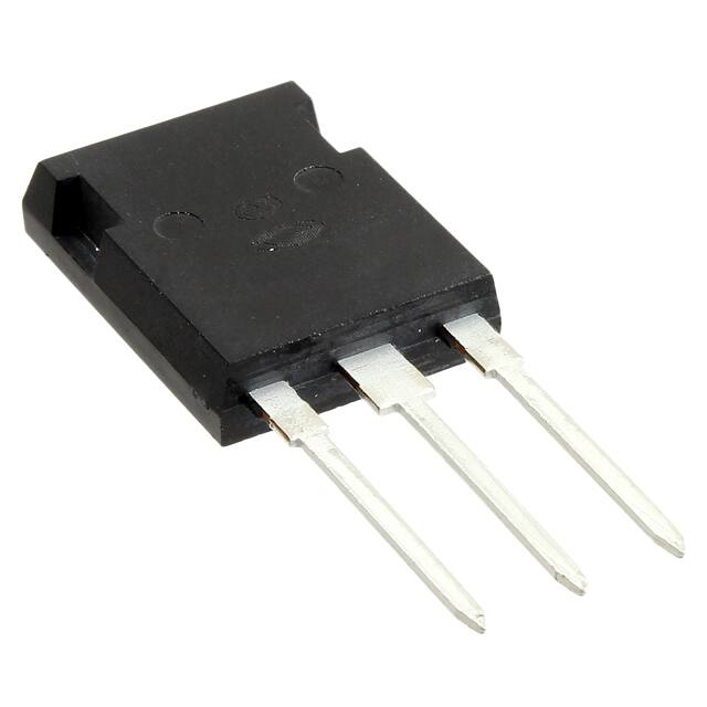
TO-247
SLL
D
• Increased Power Dissipation
• Easier To Drive
• TO-247 or Surface Mount D3PAK Package
MAXIMUM RATINGS
Symbol
0.520Ω
G
S
All Ratings: TC = 25°C unless otherwise specified.
Parameter
APT8052BLL_SLL
UNIT
800
Volts
Drain-Source Voltage
15
Continuous Drain Current @ TC = 25°C
Amps
IDM
Pulsed Drain Current
VGS
Gate-Source Voltage Continuous
±30
VGSM
Gate-Source Voltage Transient
±40
Total Power Dissipation @ TC = 25°C
298
Watts
Linear Derating Factor
2.38
W/°C
PD
TJ,TSTG
1
60
Operating and Storage Junction Temperature Range
TL
Lead Temperature: 0.063" from Case for 10 Sec.
IAR
Avalanche Current
EAR
Repetitive Avalanche Energy
EAS
Single Pulse Avalanche Energy
1
Volts
-55 to 150
°C
300
Amps
15
(Repetitive and Non-Repetitive)
1
30
4
mJ
1210
STATIC ELECTRICAL CHARACTERISTICS
MIN
BVDSS
Drain-Source Breakdown Voltage (VGS = 0V, ID = 250µA)
800
RDS(on)
Drain-Source On-State Resistance
IDSS
IGSS
VGS(th)
2
(VGS = 10V, ID = 7.5A)
TYP
MAX
Volts
0.52
Zero Gate Voltage Drain Current (VDS = 800V, VGS = 0V)
100
Zero Gate Voltage Drain Current (VDS = 640V, VGS = 0V, TC = 125°C)
500
Gate-Source Leakage Current (VGS = ±30V, VDS = 0V)
Gate Threshold Voltage (VDS = VGS, ID = 1mA)
Ohms
µA
±100
nA
5
Volts
3
CAUTION: These Devices are Sensitive to Electrostatic Discharge. Proper Handling Procedures Should Be Followed.
APT Website - http://www.advancedpower.com
UNIT
6-2004
Characteristic / Test Conditions
050-7058 Rev B
Symbol
�DYNAMIC CHARACTERISTICS
APT8052BLL_SLL
Test Conditions
Characteristic
Symbol
MIN
TYP
Ciss
Input Capacitance
Coss
Output Capacitance
VDS = 25V
405
Reverse Transfer Capacitance
f = 1 MHz
60
VGS = 10V
75
VDD = 400V
11
Crss
Qg
Total Gate Charge
Qgs
Gate-Source Charge
Qgd
Gate-Drain ("Miller") Charge
td(on)
Turn-on Delay Time
tr
ID = 15A @ 25°C
tf
6
VDD = 400V
RG = 1.6Ω
Eon
Turn-on Switching Energy
Eoff
Turn-off Switching Energy
Eon
Turn-on Switching Energy
Eoff
Turn-off Switching Energy
7
INDUCTIVE SWITCHING @ 25°C
6
215
VDD = 533V, VGS = 15V
ID = 15A, RG = 5Ω
90
INDUCTIVE SWITCHING @ 125°C
6
ns
23
ID = 15A @ 25°C
Fall Time
nC
9
VGS = 15V
Turn-off Delay Time
pF
50
RESISTIVE SWITCHING
Rise Time
td(off)
UNIT
2035
VGS = 0V
3
MAX
µJ
420
VDD = 533V, VGS = 15V
ID = 15A, RG = 5Ω
110
SOURCE-DRAIN DIODE RATINGS AND CHARACTERISTICS
Symbol
MIN
Characteristic / Test Conditions
TYP
MAX
15
UNIT
IS
Continuous Source Current (Body Diode)
ISM
Pulsed Source Current
1
VSD
Diode Forward Voltage
2
t rr
Reverse Recovery Time (IS = -15A, dl S/dt = 100A/µs)
650
ns
Q
Reverse Recovery Charge (IS = -15A, dl S/dt = 100A/µs)
9.0
µC
rr
dv/
dt
Peak Diode Recovery
dv/
60
(Body Diode)
1.3
(VGS = 0V, IS = -15A)
dt
Amps
Volts
10
V/ns
MAX
UNIT
5
THERMAL CHARACTERISTICS
Symbol
Characteristic
MIN
RθJC
Junction to Case
RθJA
Junction to Ambient
TYP
0.45
40
1 Repetitive Rating: Pulse width limited by maximum junction
temperature
2 Pulse Test: Pulse width < 380 µs, Duty Cycle < 2%
3 See MIL-STD-750 Method 3471
4 Starting Tj = +25°C, L = 10.76mH, RG = 25Ω, Peak IL = 15A
5 dv/dt numbers reflect the limitations of the test circuit rather than the
device itself. IS ≤ -ID15A di/dt ≤ 700A/µs VR ≤ 800 TJ ≤ 150°C
6 Eon includes diode reverse recovery. See figures 18, 20.
APT Reserves the right to change, without notice, the specifications and information contained herein.
0.9
0.35
0.7
0.30
0.25
0.5
0.20
Note:
0.15
PDM
Z JC, THERMAL IMPEDANCE (°C/W)
θ
050-7058 Rev B
6-2004
0.45
0.40
0.3
0.10
0
Duty Factor D = t1/t2
0.1
Peak TJ = PDM x ZθJC + TC
0.05
10-5
t1
t2
SINGLE PULSE
0.05
10-4
10-3
°C/W
10-2
10-1
RECTANGULAR PULSE DURATION (SECONDS)
FIGURE 1, MAXIMUM EFFECTIVE TRANSIENT THERMAL IMPEDANCE, JUNCTION-TO-CASE vs PULSE DURATION
1.0
�Typical Performance Curves
APT8052BLL_SLL
RC MODEL
Junction
temp. (°C)
0.164
0.00592F
Power
(watts)
0.257
0.125F
ID, DRAIN CURRENT (AMPERES)
40
Case temperature. (°C)
35
30
7V
25
6.5V
20
15
6V
10
5.5V
5
5V
30
25
20
15
TJ = +125°C
TJ = -55°C
5
0
TJ = +25°C
0
2
4
6
8
10
VGS, GATE-TO-SOURCE VOLTAGE (VOLTS)
FIGURE 4, TRANSFER CHARACTERISTICS
BVDSS, DRAIN-TO-SOURCE BREAKDOWN
VOLTAGE (NORMALIZED)
ID, DRAIN CURRENT (AMPERES)
14
12
10
8
6
4
2
0
25
I
D
V
1.20
VGS=10V
1.10
1.00
VGS=20V
0.90
0.80
0
5
10
15
20
25
30
ID, DRAIN CURRENT (AMPERES)
FIGURE 5, RDS(ON) vs DRAIN CURRENT
1.10
1.05
1.00
0.95
0.90
-50
= 7.5A
GS
= 10V
1.5
1.0
0.5
0.0
-50
D
-25
0
25
50 75 100 125 150
TJ, JUNCTION TEMPERATURE (°C)
FIGURE 7, BREAKDOWN VOLTAGE vs TEMPERATURE
1.2
-25
0
25 50
75 100 125 150
TJ, JUNCTION TEMPERATURE (°C)
FIGURE 8, ON-RESISTANCE vs. TEMPERATURE
VGS(TH), THRESHOLD VOLTAGE
(NORMALIZED)
RDS(ON), DRAIN-TO-SOURCE ON RESISTANCE
(NORMALIZED)
50
75
100
125
150
TC, CASE TEMPERATURE (°C)
FIGURE 6, MAXIMUM DRAIN CURRENT vs CASE TEMPERATURE
2.5
NORMALIZED TO
= 10V @ I = 7.5A
GS
1.30
1.15
16
2.0
V
1.1
1.0
0.9
0.8
0.7
0.6
-50
-25
0
25
50
75 100 125 150
TC, CASE TEMPERATURE (°C)
FIGURE 9, THRESHOLD VOLTAGE vs TEMPERATURE
6-2004
10
0
5
10
15
20
25
30
VDS, DRAIN-TO-SOURCE VOLTAGE (VOLTS)
FIGURE 3, LOW VOLTAGE OUTPUT CHARACTERISTICS
1.40
050-7058 Rev B
ID, DRAIN CURRENT (AMPERES)
VDS> ID (ON) x RDS (ON)MAX.
250 µSEC. PULSE TEST
@