APT97N65B2C6
APT97N65LC6
650V
97A
0.041Ω
APT97N65B2C6
COOLMOS
Super Junction MOSFET
Power Semiconductors
T-Max®
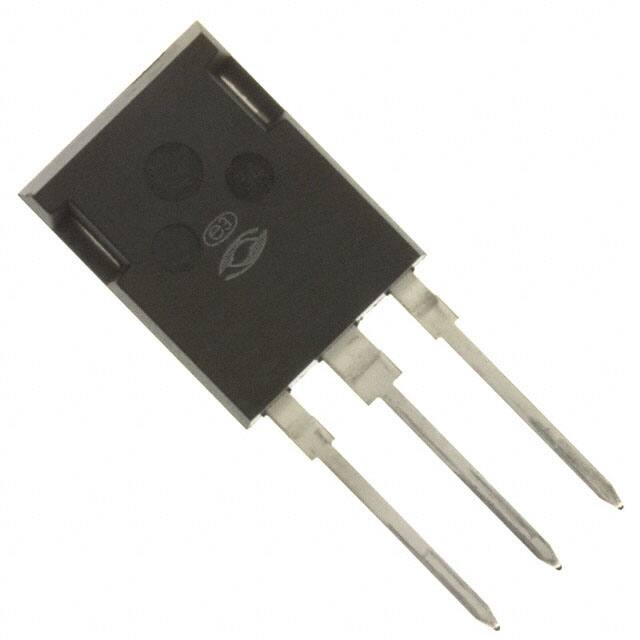
TO-264
• Ultra Low RDS(ON)
• Low Miller Capacitance
• Ultra Low Gate Charge, Qg
• Avalanche Energy Rated
APT97N65LC6
• Extreme dv/dt Rated
D
G
Unless stated otherwise, Microsemi discrete MOSFETs contain a single MOSFET die. This device is made with
two parallel MOSFET die. It is intended for switch-mode operation. It is not suitable for linear mode operation.
All Ratings per die: TC = 25°C unless otherwise specified.
MAXIMUM RATINGS
Symbol
VDSS
ID
S
Parameter
APT97N65B2_LC6
UNIT
650
Volts
Drain-Source Voltage
Continuous Drain Current @ TC = 25°C
1
97
(assuming Rdson max = 0.041Ω)
Amps
62
Continuous Drain Current @ TC = 100°C
2
291
IDM
Pulsed Drain Current
VGS
Gate-Source Voltage Continuous
±20
Volts
PD
Total Power Dissipation @ TC = 25°C
862
Watts
TJ,TSTG
Operating and Storage Junction Temperature Range
TL
Lead Temperature: 0.063" from Case for 10 Sec.
IAR
Avalanche Current
EAR
Repetitive Avalanche Energy
EAS
Single Pulse Avalanche Energy
-55 - to 150
°C
260
2
13.4
3
Amps
2.96
( Id = 13.4A, Vdd = 50V )
1954
( Id = 13.4A, Vdd = 50V )
mJ
STATIC ELECTRICAL CHARACTERISTICS
BV(DSS)
Drain-Source Breakdown Voltage (VGS = 0V, ID = 250μA)
RDS(on)
Drain-Source On-State Resistance
IDSS
IGSS
VGS(th)
MIN
4
TYP
MAX
650
Volts
0.037
(VGS = 10V, ID = 48.5A)
UNIT
0.041
Ohms
Zero Gate Voltage Drain Current (VDS = 650V, VGS = 0V)
25
Zero Gate Voltage Drain Current (VDS = 650V, VGS = 0V, TC = 150°C)
250
Gate-Source Leakage Current (VGS = ±20V, VDS = 0V)
±100
nA
3.5
Volts
Gate Threshold Voltage (VDS = VGS, ID = 2.96mA)
2.5
3
CAUTION: These Devices are Sensitive to Electrostatic Discharge. Proper Handling Procedures Should Be Followed.
"COOLMOS™ comprise a new family of transistors developed by Infineon Technologies AG. "COOLMOS" is a trademark of Infineon Technologies AG."
Microsemi Website - http://www.microsemi.com
μA
2-2011
Characteristic / Test Conditions
050-7212 Rev A
Symbol
�APT97N65B2_LC6
DYNAMIC CHARACTERISTICS
Symbol Characteristic
Ciss
Test Conditions
Input Capacitance
Coss
Reverse Transfer Capacitance
Qg
Total Gate Charge 5
Qgs
Gate-Source Charge
Qgd
Gate-Drain ("Miller ") Charge
td(on)
Turn-on Delay Time
tr
tf
Fall Time
Eon
Turn-on Switching Energy
Eoff
Turn-off Switching Energy
Eon
Turn-on Switching Energy
Eoff
Turn-off Switching Energy
6
pF
550
300
50
nC
160
25
60
ns
275
130
2860
INDUCTIVE SWITCHING @ 25°C
VDD = 433V, VGS = 15V
ID = 97A, RG = 2.2Ω
6
UNIT
7650
INDUCTIVE SWITCHING
VGS = 15V
VDD = 433V
ID = 97A @ 25°C
RG = 2.2Ω
Turn-off Delay Time
MAX
5045
VGS = 10V
VDD = 325V
ID = 97A @ 25°C
Rise Time
td(off)
TYP
VGS = 0V
VDS = 25V
f = 1 MHz
Output Capacitance
Crss
MIN
3500
μJ
4030
INDUCTIVE SWITCHING @ 125°C
VDD = 433V, VGS = 15V
ID =97A, RG = 2.2Ω
3695
SOURCE-DRAIN DIODE RATINGS AND CHARACTERISTICS
Symbol
Characteristic / Test Conditions
MIN
TYP
MAX
IS
Continuous Source Current (Body Diode)
97
ISM
Pulsed Source Current
291
VSD
Diode Forward Voltage
(Body Diode)
2
(VGS = 0V, IS = -48.5A)
4
0.9
UNIT
Amps
1.2
Volts
50
V/ns
/dt
Peak Diode Recovery /dt
t rr
Reverse Recovery Time
(IS = -97A, di/dt = 100A/μs)
Tj = 25°C
790
ns
Q rr
Reverse Recovery Charge
(IS = -97A, di/dt = 100A/μs)
Tj = 25°C
19
μC
IRRM
Peak Recovery Current
(IS = -97A, di/dt = 100A/μs)
Tj = 25°C
43
Amps
dv
dv
7
THERMAL CHARACTERISTICS
Symbol
Characteristic
RθJC
Junction to Case
RθJA
Junction to Ambient
MIN
TYP
MAX
UNIT
0.145
°C/W
40
1 Continuous current limited by package lead temperature.
4 Pulse Test: Pulse width < 380 μs, Duty Cycle < 2%
2 Repetitive Rating: Pulse width limited by maximum junction temperature
5 See MIL-STD-750 Method 3471
3 Repetitive avalanche causes additional power losses that can be calculated as 6 Eon includes diode reverse recovery.
PAV = EAR*f . Pulse width tp limited by Tj max.
7 Maximum 125°C diode commutation speed = di/dt 600A/μs
Microsemi reserves the right to change, without notice, the specifications and information contained herein.
D = 0.9
0.14
0.12
0.7
0.10
0.5
0.08
Note:
0.06
PDM
ZθJC, THERMAL IMPEDANCE (°C/W)
050-7212 Rev A
2-2011
0.16
0.3
t1
0.04
t2
0.02
t
Duty Factor D = 1/t2
Peak TJ = PDM x ZθJC + TC
0.1
SINGLE PULSE
0.05
0
10
-5
10
-4
10
-3
10-2
0.1
1
RECTANGULAR PULSE DURATION (SECONDS)
Figure 1, Maximum Effective Transient Thermal Impedance, Junction-To-Case vs Pulse Duration
10
�APT97N65B2_LC6
Typical Performance Curves
225
15V
200
140
120
7V
ID, DRAIN CURRENT (A)
150
6.5V
125
6V
100
75
5.5V
50
5V
25
100
80
60
40
TJ= 125°C
0
0
0
5
10
15
20
25
30
VDS, DRAIN-TO-SOURCE VOLTAGE (V)
FIGURE 2, Low Voltage Output Characteristics
2.00
NORMALIZED TO
V
GS
VGS = 20V
8
80
60
40
20
0.40
0
1.15
1.10
1.05
1.00
0.95
0.90
-50
0
50
100
25
50
75
100
125
150
TC, CASE TEMPERATURE (C°)
FIGURE 5, Maximum Drain Current vs Case Temperature
3.00
RDS(ON), DRAIN-TO-SOURCE ON
RESISTANCE (NORMALIZED)
1.20
100
150
200
250
ID, DRAIN CURRENT (A)
FIGURE 4, RDS(ON) vs Drain Current
0
50
2.50
2.00
1.50
1.00
0.50
0
-50
150
TJ, Junction Temperature (°C)
FIGURE 6, Breakdown Voltage vs Temperature
-25
0
25 50 75 100 125 150
TJ, JUNCTION TEMPERATURE (C°)
FIGURE 7, On-Resistance vs Temperature
1000
1.20
Rds On
ID, DRAIN CURRENT (A)
1.10
1.00
0.90
0.80
100
10µs
10
-50
0
50
100
150
TC, Case Temperature (°C)
FIGURE 8, Threshold Voltage vs Temperature
1ms
10ms
100ms
1
0.10
0.70
100µs
1
10
100
1000
VDS, DRAIN-TO-SOURCE VOLTAGE (V)
FIGURE 9, Maximum Safe Operating Area
2-2011
IDR, REVERSE
0.80
VGS(TH), THRESHOLD VOLTAGE
(NORMALIZED)
1
2
3
4
5
6
7
VGS, GATE-TO-SOURCE VOLTAGE (V)
FIGURE 3, Transfer Characteristics
100
ID, DRAIN CURRENT (A)
VGS = 10V
1.20
0.85
0
TJ= -55°C
= 10V @ 48.5A
1.60
0
TJ= 25°C
20
4.5V
050-7212 Rev A
IC, DRAIN CURRENT (A)
175
BVDSS, DRAIN-TO-SOURCE BREAKDOWN
VOLTAGE (NORMALIZED)
VDS> ID (ON) x RDS (ON)MAX.
250μSEC. PULSE TEST
@