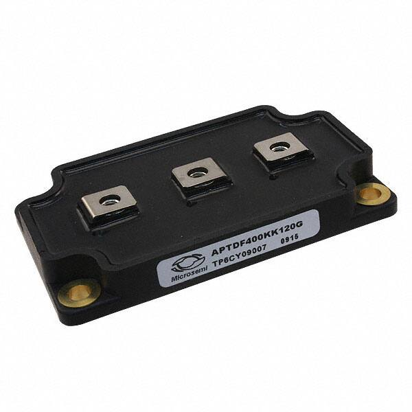
APTDF400KK120G
VCES = 1200V
IC = 400A @ Tc = 60°C
Dual Common Cathode diodes
Power Module
Application
A1
K
Uninterruptible Power Supply (UPS)
Induction heating
Welding equipment
High speed rectifiers
Features
A2
Ultra fast recovery times
Soft recovery characteristics
High blocking voltage
High current
Low leakage current
Very low stray inductance
- Symmetrical design
- M5 power connectors
High level of integration
Benefits
Outstanding performance at high frequency
operation
Low losses
Low noise switching
Direct mounting to heatsink (isolated package)
Low junction to case thermal resistance
RoHS Compliant
Symbol
VR
VRRM
Parameter
Maximum DC reverse Voltage
Maximum Peak Repetitive Reverse Voltage
IF(AV)
Maximum Average Forward
Current
IF(RMS)
IFSM
RMS Forward Current
Duty cycle = 50%
Non-Repetitive Forward Surge Current
8.3ms
Duty cycle = 50%
Max ratings
Unit
1200
V
TC = 25°C
470
TC = 60°C
TC = 45°C
TC = 45°C
400
500
3000
A
These Devices are sensitive to Electrostatic Discharge. Proper Handling Procedures Should Be Followed. See application note
APT0502 on www.microsemi.com
www.microsemi.com
1-5
APTDF400KK120G – Rev 2 October, 2012
Absolute maximum ratings
�APTDF400KK120G
All ratings @ Tj = 25°C unless otherwise specified
Electrical Characteristics
Symbol Characteristic
VF
Diode Forward Voltage
IRM
Maximum Reverse Leakage Current
CT
Junction Capacitance
Test Conditions
IF = 400A
IF = 600A
Tj = 125°C
IF = 400A
Tj = 25°C
VR = 1200V
Tj = 125°C
Min
Typ
2.4
2.7
1.8
Max
3.0
V
250
1000
VR = 1200V
Unit
440
µA
pF
Dynamic Characteristics
Symbol Characteristic
trr
Reverse Recovery Time
trr
Reverse Recovery Time
Qrr
Reverse Recovery Charge
IRRM
Reverse Recovery Current
trr
Reverse Recovery Time
Qrr
Reverse Recovery Charge
IRRM
Reverse Recovery Current
Test Conditions
IF=1A,VR=30V
di/dt = 400A/µs
IF = 400A
VR = 800V
di/dt = 800A/µs
IF = 400A
VR = 800V
Min
Typ
Tj = 25°C
45
Tj = 25°C
385
Tj = 125°C
480
Tj = 25°C
Tj = 125°C
4.2
20.9
Tj = 25°C
24
Tj = 125°C
76
Tj = 125°C
di/dt = 4000A/µs
Max
Unit
ns
ns
µC
A
210
ns
38
µC
280
A
Thermal and package characteristics
Characteristic
Junction to Case Thermal Resistance
Min
RMS Isolation Voltage, any terminal to case t =1 min, 50/60Hz
Torque
Mounting torque
4000
-40
-40
-40
3
2
Wt
Package Weight
Operating junction temperature range
Storage Temperature Range
Operating Case Temperature
To heatsink
For terminals
www.microsemi.com
M6
M5
Typ
Max
0.14
175
125
100
5
3.5
300
Unit
°C/W
V
°C
N.m
g
2-5
APTDF400KK120G – Rev 2 October, 2012
Symbol
RthJC
VISOL
TJ
TSTG
TC
�APTDF400KK120G
Typical Performance Curve
Maximum Effective Transient Thermal Impedance, Junction to Case vs Pulse Duration
Thermal Impedance (°C/W)
0.16
0.14
0.9
0.12
0.7
0.1
0.08
0.5
0.06
0.3
0.04
0.1
0.05
0.02
Single Pulse
0
0.00001
0.0001
0.001
0.01
0.1
1
10
Rectangular Pulse Duration (Seconds)
Forward Current vs Forward Voltage
Trr vs. Current Rate of Charge
TJ=175°C
800
TJ=125°C
600
400
TJ=-55°C
200
TJ=25°C
0
0.0
0.5
1.0
1.5
2.0
2.5
3.0
600
TJ=125°C
VR=800V
500
400
600 A
300
400 A
200
200 A
100
0
0
3.5
800 1600 2400 3200 4000 4800
-diF/dt (A/µs)
IRRM vs. Current Rate of Charge
QRR vs. Current Rate Charge
48
TJ=125°C
VR=800V
600 A
40
400 A
32
24
200 A
16
0
800
1600 2400 3200 4000 4800
IRRM, Reverse Recovery Current (A)
QRR, Reverse Recovery Charge (µC)
VF, Anode to Cathode Voltage (V)
300
TJ=125°C
VR=800V
250
200 A
150
100
50
0
800 1600 2400 3200 4000 4800
-diF/dt (A/µs)
Capacitance vs. Reverse Voltage
Max. Average Forward Current vs. Case Temp.
600
2500
500
2000
400
IF(AV) (A)
C, Capacitance (pF)
400 A
200
-diF/dt (A/µs)
3000
600 A
1500
1000
Duty Cycle = 0.5
TJ=175°C
300
200
100
500
0
0
1
10
100
VR, Reverse Voltage (V)
1000
0
25
50
75
100
125
150
175
Case Temperature (ºC)
www.microsemi.com
3-5
APTDF400KK120G – Rev 2 October, 2012
1000
trr, Reverse Recovery Time (ns)
IF, Forward Current (A)
1200
�APTDF400KK120G
www.microsemi.com
4-5
APTDF400KK120G – Rev 2 October, 2012
SP6 Package outline (dimensions in mm)
�APTDF400KK120G
DISCLAIMER
The information contained in the document (unless it is publicly available on the Web without access restrictions) is
PROPRIETARY AND CONFIDENTIAL information of Microsemi and cannot be copied, published, uploaded, posted,
transmitted, distributed or disclosed or used without the express duly signed written consent of Microsemi. If the
recipient of this document has entered into a disclosure agreement with Microsemi, then the terms of such Agreement
will also apply. This document and the information contained herein may not be modified, by any person other than
authorized personnel of Microsemi. No license under any patent, copyright, trade secret or other intellectual property
right is granted to or conferred upon you by disclosure or delivery of the information, either expressly, by implication,
inducement, estoppels or otherwise. Any license under such intellectual property rights must be approved by
Microsemi in writing signed by an officer of Microsemi.
Microsemi reserves the right to change the configuration, functionality and performance of its products at anytime
without any notice. This product has been subject to limited testing and should not be used in conjunction with lifesupport or other mission-critical equipment or applications. Microsemi assumes no liability whatsoever, and Microsemi
disclaims any express or implied warranty, relating to sale and/or use of Microsemi products including liability or
warranties relating to fitness for a particular purpose, merchantability, or infringement of any patent, copyright or other
intellectual property right. Any performance specifications believed to be reliable but are not verified and customer or
user must conduct and complete all performance and other testing of this product as well as any user or customers final
application. User or customer shall not rely on any data and performance specifications or parameters provided by
Microsemi. It is the customer’s and user’s responsibility to independently determine suitability of any Microsemi
product and to test and verify the same. The information contained herein is provided “AS IS, WHERE IS” and with all
faults, and the entire risk associated with such information is entirely with the User. Microsemi specifically disclaims
any liability of any kind including for consequential, incidental and punitive damages as well as lost profit. The product
is subject to other terms and conditions which can be located on the web at http://www.microsemi.com/legal/tnc.asp
Life Support Application
Seller's Products are not designed, intended, or authorized for use as components in systems intended for space,
aviation, surgical implant into the body, in other applications intended to support or sustain life, or for any other
application in which the failure of the Seller's Product could create a situation where personal injury, death or property
damage or loss may occur (collectively "Life Support Applications").
Buyer agrees not to use Products in any Life Support Applications and to the extent it does it shall conduct extensive
testing of the Product in such applications and further agrees to indemnify and hold Seller, and its officers, employees,
subsidiaries, affiliates, agents, sales representatives and distributors harmless against all claims, costs, damages and
expenses, and attorneys' fees and costs arising, directly or directly, out of any claims of personal injury, death, damage
or otherwise associated with the use of the goods in Life Support Applications, even if such claim includes allegations
that Seller was negligent regarding the design or manufacture of the goods.
www.microsemi.com
5-5
APTDF400KK120G – Rev 2 October, 2012
Buyer must notify Seller in writing before using Seller’s Products in Life Support Applications. Seller will study with
Buyer alternative solutions to meet Buyer application specification based on Sellers sales conditions applicable for the
new proposed specific part.
�