AT21CS01/AT21CS11
Single-Wire, I/O Powered 1-Kbit (128 x 8) Serial EEPROM
with a Unique, Factory-Programmed 64-Bit Serial Number
Features
•
•
•
•
•
•
•
•
•
•
•
•
•
•
Low‑Voltage Operation:
– AT21CS01 is self-powered via the 1.7V to 3.6V pull‑up voltage on the SI/O line
– AT21CS11 is self-powered via the 2.7V to 4.5V pull‑up voltage on the SI/O line
Internally Organized as 128 x 8 (1 Kbit)
Industrial Temperature Range: -40°C to +85°C
Single-Wire Serial Interface with I2C Protocol Structure:
– Device communication is achieved through a single I/O pin
Standard Speed and High-Speed Mode Options:
– 15.4 kbps maximum bit rate in Standard Speed mode (AT21CS01 only)
– 125 kbps maximum bit rate in High-Speed mode (AT21CS01 and AT21CS11)
8‑Byte Page Write or Single Byte Writes Allowed
Discovery Response Feature for Quick Detection of Devices on the Bus
ROM Zone Support:
– Device is segmented into four 256‑bit zones, each of which can be permanently made read‑only (ROM)
256‑Bit Security Register:
– Lower eight bytes contain a factory-programmed, read-only, 64‑bit serial number that is unique to all
Microchip single‑wire devices
– Next eight bytes are reserved for future use and will read FFh
– Upper 16 bytes are user‑programmable and permanently lockable
Self‑Timed Write Cycle: 5 ms Maximum
Manufacturer Identification Register:
– Device responds with unique value for Microchip as well as density and revision information
High Reliability:
– Endurance: 1,000,000 write cycles
– Data retention: 100 years
– IEC 61000-4-2 Level 4 ESD Compliant (±8 kV Contact, ±15 kV Air Discharge)
Green (Lead-free/Halide-free/RoHS Compliant) Package Options
Die Sale Options: Wafer Form and Tape and Reel
Packages
•
2-Pad XSFN, 3-Lead SOT23, 8-Lead SOIC and 4-Ball WLCSP
© 2020 Microchip Technology Inc.
Datasheet
DS20005857D-page 1
�AT21CS01/AT21CS11
Package Types
3-Lead SOT23
(Top View)
2-Pad XSFN
(Top View)
1
2 NC
SI/O
GND 3
2
GND
1 SI/O
8-Lead SOIC
(Top View)
4-Ball WLCSP
(Top View)
NC
1
8
NC
NC
2
7
NC
NC
3
6
NC
GND
4
© 2020 Microchip Technology Inc.
5
SI/O
SI/O
A1
A2
NC
GND
B1
B2
NC
Datasheet
DS20005857D-page 2
�AT21CS01/AT21CS11
Table of Contents
Features......................................................................................................................................................... 1
Packages........................................................................................................................................................1
Package Types...............................................................................................................................................2
1.
Pin Descriptions...................................................................................................................................... 5
1.1.
1.2.
2.
Description.............................................................................................................................................. 6
2.1.
2.2.
3.
EEPROM Access (Opcode Ah)..................................................................................................19
Security Register Access (Opcode Bh)...................................................................................... 19
Lock Security Register (Opcode 2h).......................................................................................... 19
ROM Zone Register Access (Opcode 7h)..................................................................................19
Freeze ROM Zone State (Opcode 1h)....................................................................................... 19
Manufacturer ID Read (Opcode Ch).......................................................................................... 20
Standard Speed Mode (Opcode Dh)..........................................................................................20
High-Speed Mode (Opcode Eh)................................................................................................. 20
Write Operations................................................................................................................................... 21
7.1.
7.2.
7.3.
7.4.
7.5.
7.6.
8.
Memory Organization................................................................................................................. 17
Available Opcodes................................................................................................................................ 19
6.1.
6.2.
6.3.
6.4.
6.5.
6.6.
6.7.
6.8.
7.
Single-Wire Bus Transactions.................................................................................................... 12
Device Addressing and I2C Protocol Emulation.................................................................................... 17
5.1.
6.
Absolute Maximum Ratings..........................................................................................................8
DC and AC Operating Range.......................................................................................................8
AT21CS01 DC Characteristics(1)..................................................................................................8
AT21CS11 DC Characteristics(1).................................................................................................. 9
AT21CS01/AT21CS11 AC Characteristics................................................................................. 10
Device Operation and Communication................................................................................................. 12
4.1.
5.
System Configuration Using Single-Wire Serial EEPROMs.........................................................6
Block Diagram.............................................................................................................................. 7
Electrical Characteristics.........................................................................................................................8
3.1.
3.2.
3.3.
3.4.
3.5.
4.
Serial Input and Output................................................................................................................ 5
Ground......................................................................................................................................... 5
Device Behavior During Internal Write Cycle............................................................................. 21
Byte Write...................................................................................................................................21
Page Write..................................................................................................................................21
Writing to the Security Register..................................................................................................22
Locking the Security Register.....................................................................................................23
Setting the Device Speed...........................................................................................................24
Read Operations................................................................................................................................... 25
8.1.
8.2.
Current Address Read within the EEPROM...............................................................................25
Random Read within the EEPROM........................................................................................... 25
© 2020 Microchip Technology Inc.
Datasheet
DS20005857D-page 3
�AT21CS01/AT21CS11
8.3.
8.4.
8.5.
9.
Sequential Read within the EEPROM........................................................................................ 26
Read Operations in the Security Register.................................................................................. 26
Manufacturer ID Read................................................................................................................ 27
ROM Zones...........................................................................................................................................29
9.1.
9.2.
9.3.
ROM Zone Size and ROM Zone Registers................................................................................ 29
Programming and Reading the ROM Zone Registers................................................................29
Device Response to a Write Operation Within an Enabled ROM Zone..................................... 31
10. Device Default Condition from Microchip.............................................................................................. 32
11. Packaging Information.......................................................................................................................... 33
11.1. Package Marking Information.....................................................................................................33
12. Revision History.................................................................................................................................... 42
The Microchip Website.................................................................................................................................43
Product Change Notification Service............................................................................................................43
Customer Support........................................................................................................................................ 43
Product Identification System.......................................................................................................................44
Microchip Devices Code Protection Feature................................................................................................ 45
Legal Notice................................................................................................................................................. 45
Trademarks.................................................................................................................................................. 45
Quality Management System....................................................................................................................... 46
Worldwide Sales and Service.......................................................................................................................47
© 2020 Microchip Technology Inc.
Datasheet
DS20005857D-page 4
�AT21CS01/AT21CS11
Pin Descriptions
1.
Pin Descriptions
The descriptions of the pins are listed in Table 1-1.
Table 1-1. Pin Function Table
1.1
Name
2-Pad XSFN
3-Lead SOT23
8-Lead SOIC
4-Ball WLCSP
Function
NC
—
—
1
—
No Connect
NC
—
—
2
—
No Connect
NC
—
2
3
B2
No Connect
GND
2
3
4
B1
Ground
SI/O
1
1
5
A1
Serial Input and Output
NC
—
—
6
A2
No Connect
NC
—
—
7
—
No Connect
NC
—
—
8
—
No Connect
Serial Input and Output
The SI/O pin is an open-drain, bidirectional input/output pin used to serially transfer data to and from the device. The
SI/O pin must be pulled high using an external pull‑up resistor and may be wire-ORed with any number of other
open‑drain or open‑collector pins from other devices on the same bus. The device also uses the SI/O pin as its
voltage source by drawing and storing power during the periods that the pin is pulled high to a voltage level between
1.7V to 3.6V (AT21CS01) and between 2.7V to 4.5V (AT21CS11).
1.2
Ground
The ground reference for the power supply. GND should be connected to the system ground.
© 2020 Microchip Technology Inc.
Datasheet
DS20005857D-page 5
�AT21CS01/AT21CS11
Description
2.
Description
The AT21CS01/AT21CS11 is a 2-pin memory (SI/O and Ground) that harvests energy from the SI/O pin to power the
integrated circuit. It provides 1,024 bits of Serial Electrically Erasable and Programmable Read-Only Memory
(EEPROM) organized as 128 words of eight bits each.
The device is optimized to add configuration and use information in unpowered attachments using a two-point
mechanical connection that brings only one signal (SI/O) and GND to the unpowered attachment. Some unpowered
attachment application examples include analog sensor calibration data storage, ink and toner printer cartridge
identification, and management of after‑market consumables. The device’s software addressing scheme allows up to
eight devices to share a common single‑wire bus. The device is available in space‑saving package options and
operates with an external pull‑up voltage from 1.7V to 3.6V on the SI/O line (AT21CS01) or from 2.7V to 4.5V on the
SI/O line (AT21CS11).
2.1
System Configuration Using Single-Wire Serial EEPROMs
VPUP
RPUP
(See Sections 3.3 and 3.4 for requirements.)
VCC
SI/O
Bus Master:
Microcontroller
GND
© 2020 Microchip Technology Inc.
SI/O
SI/O
SI/O
Slave 0
AT21CSXX
Slave 1
AT21CSXX
Slave 7
AT21CSXX
GND
GND
GND
Datasheet
DS20005857D-page 6
�AT21CS01/AT21CS11
Description
Block Diagram
Device
Configuration
Latches
Memory
System Control
Module
Device
Power
Extraction
SI/O
High Voltage
Generation Circuit
Reset
Detection
Row Decoder
2.2
EEPROM Array
Command
Control
1 page
Column Decoder
Data Register
Data & ACK
DOUT Input/Output Control
Internal
Timing
Generation
DIN
GND
© 2020 Microchip Technology Inc.
Datasheet
DS20005857D-page 7
�AT21CS01/AT21CS11
Electrical Characteristics
3.
Electrical Characteristics
3.1
Absolute Maximum Ratings
Temperature under bias
-55°C to +125°C
Storage temperature
-65°C to +150°C
Voltage on any pin with respect to ground
-0.6V to VPUP +0.5V
DC output current
15.0 mA
Note: Stresses above those listed under “Absolute Maximum Ratings” may cause permanent damage to the device.
This is a stress rating only and functional operation of the device at these or any other conditions above those
indicated in the operation listings of this specification is not implied. Exposure to absolute maximum rating conditions
for extended periods may affect device reliability.
3.2
DC and AC Operating Range
Table 3-1. DC and AC Operating Range
3.3
AT21CS01
AT21CS11
Operating Temperature (Case)
Industrial Temperature Range
-40°C to +85°C
-40°C to +85°C
VPUP Pull-up Voltage
Voltage Range
1.7V to 3.6V
2.7V to 4.5V
AT21CS01 DC Characteristics(1)
Parameter
Pull-up Voltage
Pull-up Resistance
Symbol
Minimum
Typical(2)
Maximum
Units
VPUP
1.7
—
3.6
V
High-Speed mode
2.7
—
3.6
V
Standard Speed mode
130
—
200
Ω
VPUP = 1.7V
0.2
—
1.8
kΩ
VPUP = 2.7V
0.33
—
4
kΩ
VPUP = 3.6V
RPUP
Test Conditions
Active Current, Read
IA1
—
0.08
0.3
mA
VPUP = 3.6V;
SI/O = VPUP
Active Current, Write
IA2
—
0.2
0.5
mA
VPUP = 3.6V
Standby Current
ISB
—
0.6
1.5
µA
VPUP = 1.8V(3);
SI/O = VPUP
—
0.7
2.5
µA
VPUP = 3.6V
Input Low Level(3)(4)
VIL
–0.6
—
0.5
V
Input High Level(3)(4)
VIH
VPUP x 0.7
—
VPUP + 0.5
V
VHYS
0.128
—
1.17
V
Output Low Level
VOL
0
—
0.4
V
Bus Capacitance
CBUS
—
—
1000
pF
SI/O
Hysteresis(3)(4)(5)
© 2020 Microchip Technology Inc.
Datasheet
IOL = 4 mA
DS20005857D-page 8
�AT21CS01/AT21CS11
Electrical Characteristics
Notes:
1. Parameters are applicable over the operating range in DC and AC Operating Range, unless otherwise noted.
2. Typical values characterized at TA = +25°C unless otherwise noted.
3. This parameter is characterized but is not 100% tested in production.
4. VIH, VIL, and VHYS are a function of the internal supply voltage, which is a function of VPUP, RPUP, CBUS, and
timing used. Use of a lower VPUP, higher RPUP, higher CBUS, and shorter tRCV creates lower VIH, VIL and VHYS
values.
5. Once VIH is crossed on a rising edge of SI/O, the voltage on SI/O must drop at least by VHYS to be detected as
a logic ‘0’.
3.4
AT21CS11 DC Characteristics(1)
Symbol
Minimum
Typical(2)
Maximum
Units
Pull-up Voltage
VPUP
2.7
—
4.5
V
High-Speed mode
Pull-up Resistance
RPUP
0.2
—
1.8
kΩ
VPUP = 2.7V
0.4
—
5.4
kΩ
VPUP = 4.5V
Parameter
Test Conditions
Active Current, Read
IA1
—
0.08
0.3
mA
VPUP = 4.5V;
SI/O = VPUP
Active Current, Write
IA2
—
0.2
0.5
mA
VPUP = 4.5V
Standby Current
ISB
—
0.6
1.5
µA
VPUP = 2.7V(3);
SI/O = VPUP
—
0.7
3.0
µA
VPUP = 4.5V;
SI/O = VPUP
Input Low Level(3)(4)
VIL
–0.6
—
0.5
V
Level(3)(4)
VIH
VPUP x 0.7
—
VPUP + 0.5
V
SI/O Hysteresis(3)(4)(5)
VHYS
0.128
—
1.4
V
Output Low Level
VOL
0
—
0.4
V
Bus Capacitance
CBUS
—
—
1000
pF
Input High
IOL = 4 mA
Notes:
1. Parameters are applicable over the operating range in DC and AC Operating Range, unless otherwise noted.
2. Typical values characterized at TA = +25°C unless otherwise noted.
3. This parameter is characterized but is not 100% tested in production.
4. VIH, VIL, and VHYS are a function of the internal supply voltage, which is a function of VPUP, RPUP, CBUS, and
timing used. Use of a lower VPUP, higher RPUP, higher CBUS, and shorter tRCV creates lower VIH, VIL and VHYS
values.
5. Once VIH is crossed on a rising edge of SI/O, the voltage on SI/O must drop at least by VHYS to be detected as
a logic ‘0’.
© 2020 Microchip Technology Inc.
Datasheet
DS20005857D-page 9
�AT21CS01/AT21CS11
Electrical Characteristics
3.5
AT21CS01/AT21CS11 AC Characteristics
3.5.1
Reset and Discovery Response Timing
Parameter and Condition(1)(2)
Symbol
Standard
Speed(3)(4)
High Speed
Units
Min.
Max.
Min.
Max.
Reset Low Time, Device in Inactive State
tRESET
480
—
96
—
µs
Discharge Low Time, Device in Active
Write Cycle (tWR)
tDSCHG
150
—
150
—
µs
tRRT
N/A
N/A
8
—
Reset Recovery Time
µs
(5)
Discovery Response Request
tDRR
N/A
N/A
1
2 - tPUP
µs
Discovery Response Acknowledge Time
tDACK
N/A
N/A
8
24
µs
Master Strobe Discovery Response Time
tMSDR
N/A
N/A
2
6
µs
SI/O High Time for Start/Stop Condition
tHTSS
N/A
N/A
150
—
µs
Notes:
1. Parameters applicable over operating range in DC and AC Operating Range, unless otherwise noted.
2. AC measurement conditions for the table above:
– Loading capacitance on SI/O: 100 pF
– RPUP (bus line pull-up resistor to VPUP): 1 kΩ; VPUP: 2.7V
3. Due to the fact that the device will default to High-Speed mode upon Reset, the Reset and Discovery
Response Timing after tRESET does not apply for Standard Speed mode. High-Speed mode timing applies in all
cases after tRESET.
4. Standard Speed is not available on the AT21CS11.
5. tPUP is the time required once the SI/O line is released to be pulled up from VIL to VIH. This value is application
specific and is a function of the loading capacitance on the SI/O line as well as the RPUP chosen. The use of
additional slave devices adds capacitance to the SI/O line and should be taken into consideration. Limits for
these values are provided in AT21CS01 DC Characteristics and AT21CS11 DC Characteristics.
3.5.2
Data Communication Timing
Parameter and Condition(1)(2)
Bit Frame Duration
Symbol
Frame Type
Standard Speed(3)
High Speed
Min.
Max.
Min.
Max.
Units
tBIT
Input and
Output Bit
Frame
40
100
tLOW0 +
tPUP(4) +
tRCV
25
µs
SI/O High Time for Start/Stop
Condition
tHTSS
Input Bit
Frame
600
—
150
—
µs
SI/O Low Time, Logic ‘0’ Condition
tLOW0
Input Bit
Frame
24
64
6
16
µs
SI/O Low Time, Logic ‘1’ Condition
tLOW1
Input Bit
Frame
4
8
1
2
µs
Master SI/O Low Time During Read
tRD
Output Bit
Frame
4
8tPUP(4)
1
2tPUP(4)
µs
© 2020 Microchip Technology Inc.
Datasheet
DS20005857D-page 10
�AT21CS01/AT21CS11
Electrical Characteristics
...........continued
Parameter and Condition(1)(2)
Symbol
Frame Type
Standard Speed(3)
High Speed
Min.
Max.
Min.
Max.
Units
Master Read Strobe Time
tMRS
Output Bit
Frame
tRD +
tPUP(4)
8
tRD +
tPUP(4)
2
µs
Data Output Hold Time
(Logic ‘0’)
tHLD0
Output Bit
Frame
8
24
2
6
µs
Slave Recovery Time
tRCV
Input and
Output Bit
Frame
8
—
2(5)
—
µs
tNOISE
Input Bit
Frame
0.5
—
—
—
µs
Noise Filtering Capability on SI/O
Notes:
1. Parameters applicable over operating range in DC and AC Operating Range, unless otherwise noted.
2. AC measurement conditions for the table above:
– Loading capacitance on SI/O: 100 pF
– RPUP (bus line pull-up resistor to VPUP): 1 kΩ; VPUP: 2.7V
3. Standard Speed is not available on the AT21CS11.
4. tPUP is the time required once the SI/O line is released to be pulled up from VIL to VIH. This value is application
specific and is a function of the loading capacitance on the SI/O line as well as the RPUP chosen. The use of
additional slave devices adds capacitance to the SI/O line and should be taken into consideration. Limits for
these values are provided in AT21CS01 DC Characteristics and AT21CS11 DC Characteristics.
5. The system designer must select an combination of RPUP, CBUS, and tBIT such that the minimum tRCV is
satisfied. The relationship of tRCV within the bit frame can be expressed by the following formula:
tBIT = tLOW0 + tPUP + tRCV.
3.5.3
EEPROM Cell Performance Characteristics
Operation
Min.
Max.
Units
—
5
ms
VPUP (min.) < VPUP < VPUP (max.),
TA = 25°C, Byte or Page Write mode
1,000,000
—
Write Cycles
VPUP (min.) < VPUP < VPUP (max.),
TA = 25°C, Byte or Page Write mode
100
—
Years
Write Cycle Time
(tWR)
Write Endurance(1)
Data Retention(1)
Test Condition
TA = 55°C
Note:
1. Performance is determined through characterization and the qualification process.
© 2020 Microchip Technology Inc.
Datasheet
DS20005857D-page 11
�AT21CS01/AT21CS11
Device Operation and Communication
4.
Device Operation and Communication
The AT21CS01/11 operates as a slave device and utilizes a single‑wire digital serial interface to communicate with a
host controller, commonly referred to as the bus master. The master controls all read and write operations to the
slave devices on the serial bus. The device has two speeds of operation, Standard Speed mode (AT21CS01) and
High-Speed mode (AT21CS01 and AT21CS11).
The device utilizes an 8-bit data structure. Data is transferred to and from the device via the single‑wire serial
interface using the Serial Input/Output (SI/O) pin. Power to the device is also provided via the SI/O pin, thus only the
SI/O pin and the GND pin are required for device operation. Data sent to the device over the single‑wire bus is
interpreted by the state of the SI/O pin during specific time intervals or slots. Each time slot is referred to as a bit
frame and lasts tBIT in duration. The master initiates all bit frames by driving the SI/O line low. All commands and data
information are transferred with the Most Significant bit (MSb) first.
The software sequence sent to the device is an emulation of what would be sent to an I2C Serial EEPROM with the
exception that typical 4-bit device type identifier of 1010b in the device address is replaced by a 4-bit opcode. The
device has been architected in this way to allow for rapid deployment and significant reuse of existing I2C firmware.
For more details about the way the device operates, refer to Device Addressing and I2C Protocol Emulation.
During bus communication, one data bit is transmitted in every bit frame, and after eight bits (one byte) of data has
been transferred, the receiving device must respond with either an Acknowledge (ACK) or a
No Acknowledge (NACK) response bit during a ninth bit window. There are no unused clock cycles during any read
or write operation, so there must not be any interruptions or breaks in the data stream during each data byte transfer
and ACK or NACK clock cycle. In the event where an unavoidable system interrupt is required, refer to the
requirements outlined in Communication Interruptions.
4.1
Single-Wire Bus Transactions
Types of data transmitted over the SI/O line:
•
•
Reset and Discovery Response
Logic ‘0’ or Acknowledge (ACK)
•
Logic ‘1’ or No Acknowledge (NACK)
•
•
Start Condition
Stop Condition
The Reset and Discovery Response is not considered to be part of the data stream to the device, whereas the
remaining four transactions are all required in order to send data to and receive data from the device. The difference
between the different types of data stream transactions is the duration that SI/O is driven low within the bit frame.
4.1.1
4.1.1.1
Device Reset/Power-up and Discovery Response
Resetting the Device
A Reset and Discovery Response sequence is used by the master to reset the device as well as to perform a general
bus call to determine if any devices are present on the bus.
To begin the Reset portion of the sequence, the master must drive SI/O low for a minimum time. If the device is not
currently busy with other operations, the master can drive SI/O low for a time of tRESET. The length of tRESET differs
for Standard Speed mode and for High-Speed mode.
However, if the device is busy, the master must drive SI/O for a time of tDSCHG to ensure the device is reset as
discussed in Interrupting the Device during an Active Operation. The Reset time forces any internal charge storage
within the device to be consumed, causing the device to lose all remaining standby power available internally.
Upon SI/O being released for a sufficient amount of time to allow the device time to power-up and initialize, the
master must then always request a Discovery Response Acknowledge from the AT21CS01/AT21CS11 prior to any
commands being sent to the device. The master can then determine if an AT21CS01/AT21CS11 is present by
sampling for the Discovery Response Acknowledge from the device.
© 2020 Microchip Technology Inc.
Datasheet
DS20005857D-page 12
�AT21CS01/AT21CS11
Device Operation and Communication
4.1.1.2
Device Response Upon Reset or Power-Up
After the device has been powered up or after the master has reset the device by holding the SI/O line low for tRESET
or tDSCHG, the master must then release the line which will be pulled high by an external pull-up resistor. The master
must then wait an additional minimum time of tRRT before the master can request a Discovery Response
Acknowledge from the device.
The Discovery Response Acknowledge sequence begins by the master driving the SI/O line low which will start the
AT21CS01/AT21CS11 internal timing circuits. The master must continue to drive the line low for tDRR.
During the tDRR time, the AT21CS01/AT21CS11 will respond by concurrently driving SI/O low. The device will
continue to drive SI/O low for a total time of tDACK. The master should sample the state of the SI/O line at tMSDR past
the initiation of tDRR. By definition, the tDACK minimum is longer than the tMSDR maximum time, thereby ensuring the
master can always correctly sample the SI/O for a level less than VIL. After the tDACK time has elapsed, the
AT21CS01/AT21CS11 will release SI/O which will then be pulled high by the external pull‑up resistor.
The master must then wait tHTSS to create a Start condition before continuing with the first command (see Start/Stop
Condition for more details about Start conditions). By default, the device will come out of Reset in High-Speed mode.
Changing the device to Standard Speed mode is covered in Standard Speed Mode (Opcode Dh).
The timing requirements for the Reset and Discovery Response sequence for both Standard Speed and High-Speed
mode can be found in AT21CS01/AT21CS11 AC Characteristics.
4.1.2
Interrupting the Device during an Active Operation
To conserve the stored energy within the onboard parasitic power system and minimize overall active current, the
AT21CS01/AT21CS11 will not monitor the SI/O line for new commands while it is busy executing a previously sent
command. As a result, the device is not able to sense how long SI/O has been in a given state. If the master requires
to interrupt the device during an active operation, it must drive SI/O low long enough to deplete all of its remaining
stored power. This time is defined as tDSCHG, after which a normal Discovery Response can begin by releasing the
SI/O line.
Figure 4-1. Reset and Discovery Response Waveform
MASTER
AT21CS01
PULL-UP RESISTOR
tPUP
VIH
SI/O
tDRR
VIL
tRESET
/
tDSCHG
tRRT
Master
Sampling
Window
tHTSS
Begin Next
Command with
Start Condition
tMSDR
tDACK
4.1.3
Data Input and Output Bit Frames
Communication with the AT21CS01/AT21CS11 is conducted in time intervals referred to as a bit frame and lasts tBIT
in duration. Each bit frame contains a single binary data value. Input bit frames are used to transmit data from the
master to the AT21CS01/AT21CS11 and can either be a logic ‘0’ or a logic ‘1’. An output bit frame carries data from
the AT21CS01/AT21CS11 to the master. In all input and output cases, the master initiates the bit frame by driving the
SI/O line low. Once the AT21CS01/AT21CS11 detects the SI/O being driven below the VIL level, its internal timing
circuits begin to run.
The duration of each bit frame is allowed to vary from bit to bit as long as the variation does not cause the tBIT length
to exceed the specified minimum and maximum values (see AT21CS01/AT21CS11 AC Characteristics). The tBIT
requirements will vary depending on whether the device is set for Standard Speed or High-Speed mode. For more
information about setting the speed of the device, refer to Setting the Device Speed.
4.1.3.1
Data Input Bit Frames
A data input bit frame can be used by the master to transmit either a logic ‘0’ or logic ‘1’ data bit to the AT21CS01/
AT21CS11. The input bit frame is initiated when the master drives the SI/O line low. The length of time that the SI/O
© 2020 Microchip Technology Inc.
Datasheet
DS20005857D-page 13
�AT21CS01/AT21CS11
Device Operation and Communication
line is held low will dictate whether the master is transmitting a logic ‘0’ or a logic ‘1’ for that bit frame. For a logic ‘0’
input, the length of time that the SI/O line must be held low is defined as tLOW0. Similarly, for a logic ‘1’ input, the
length of time that the SI/O line must be held low is defined as tLOW1.
The AT21CS01/AT21CS11 will sample the state of the SI/O line after the maximum tLOW1 but prior to the minimum
tLOW0 after SI/O was driven below the VIL threshold to determine if the data input is a logic ‘0’ or a logic ‘1’. If the
master is still driving the line low at the sample time, the AT21CS01/AT21CS11 will decode that bit frame as a logic
‘0’ as SI/O will be at a voltage less than VIL. If the master has already released the SI/O line, the AT21CS01/
AT21CS11 will see a voltage level greater than or equal to VIH because of the external pull-up resistor, and that bit
frame will be decoded as a logic ‘1’. The timing requirements for these parameters can be found in AT21CS01/
AT21CS11 AC Characteristics.
A logic ‘0’ condition has multiple uses in the I2C emulation sequences. It is used to signify a ‘0’ data bit, and it also is
used for an Acknowledge (ACK) response. Additionally, a logic ‘1’ condition is also is used for a No Acknowledge
(NACK) response in addition to the nominal ‘1‘ data bit.
Figure 4-2 and Figure 4-3 depict the logic ‘0’ and logic ‘1’ input bit frames.
Figure 4-2. Logic ‘0’ Input Condition Waveform
MASTER
PULL-UP RESISTOR
VIH
SI/O
VIL
tLOW0
tRCV
tBIT
Figure 4-3. Logic ‘1’ Input Condition Waveform
MASTER
PULL-UP RESISTOR
VIH
SI/O
VIL
tLOW1
tBIT
4.1.3.2
Start/Stop Condition
All transactions to the AT21CS01/AT21CS11 begin with a Start condition; therefore, a Start can only be transmitted
by the master to the slave. Likewise, all transactions are terminated with a Stop condition and thus a Stop condition
can only be transmitted by the master to the slave.
The Start and Stop conditions require identical biasing of the SI/O line. The Start/Stop condition is created by holding
the SI/O line at a voltage of VPUP for a duration of tHTSS. Refer to AT21CS01/AT21CS11 AC Characteristics for timing
minimums and maximums.
Figure 4-4 and Figure 4-5 depict the Start and Stop conditions.
© 2020 Microchip Technology Inc.
Datasheet
DS20005857D-page 14
�AT21CS01/AT21CS11
Device Operation and Communication
Figure 4-4. Start Condition Waveform
MASTER
PULL-UP RESISTOR
VIH
SI/O
VIL
tHTSS
Figure 4-5. Stop Condition Waveform
MASTER
VIH
SI/O
Previous
Bit Frame
PULL-UP RESISTOR
tRCV
VIL
tHTSS
4.1.3.3
Communication Interruptions
In the event that a protocol sequence is interrupted midstream, this sequence can be resumed at the point of
interruption if the elapsed time of inactivity (where SI/O is idle) is less that the maximum tBIT time. The maximum
allowed value will differ if the device is High-Speed mode or Standard Speed mode (see Setting the Device Speed).
Note: The interruption of protocol must not occur during a write sequence immediately after a logic ‘0’ (ACK
response) when sending data to be written to the device. In this case, the interruption will be interpreted as a Stop
condition and will cause an internal write cycle to begin. The device will be busy for tWR time and will not respond to
any commands.
For systems that cannot accurately monitor the location of interrupts, it is recommended to ensure that a minimum
interruption time be observed consistent with the longest busy operation of the device (tWR). Communicating with the
device while it is in an internal write cycle by the master driving SI/O low could cause the byte(s) being written to
become corrupted and must be avoided. The behavior of the device during a write cycle is described in more detail in
Device Behavior During Internal Write Cycles.
If the sequence is interrupted for longer than the maximum tBIT, the master must wait at least the minimum tHTSS
before continuing. By waiting the minimum tHTSS time, a new Start condition is created and the device is ready to
receive a new command. It is recommended that the master start over and repeat the transaction that was
interrupted midstream.
4.1.3.4
Data Output Bit Frame
A data output bit frame is used when the master is to receive communication back from the AT21CS01/AT21CS11.
Data output bit frames are used when reading any data out as well as any ACK or NACK responses from the device.
Just as in the input bit frame, the master initiates the sequence by driving the SI/O line below the VIL threshold which
engages the AT21CS01/AT21CS11 internal timing generation circuit.
Within the output bit frame is the critical timing parameter tRD, which is defined as the amount of time the master must
continue to drive the SI/O line low after crossing the below VIL threshold to request a data bit back from the
AT21CS01/AT21CS11. Once the tRD duration has expired, the master must release the SI/O line.
If the AT21CS01/AT21CS11 is responding with a logic ‘0’ (for either a ‘0’ data bit or an ACK response), it will begin to
pull the SI/O line low concurrently during the tRD window and continue to hold it low for a duration of tHLD0, after which
it will release the line to be pulled back up to VPUP (see Figure 4-6). Thus, when the master samples SI/O within the
© 2020 Microchip Technology Inc.
Datasheet
DS20005857D-page 15
�AT21CS01/AT21CS11
Device Operation and Communication
tMRS window, it will see a voltage less than VIL and decode this event as a logic ’0’. By definition, the tHLD0 time is
longer than the tMRS time and therefore, the master is ensured to sample while the AT21CS01/AT21CS11 is still
driving the SI/O line low.
Figure 4-6. Logic ‘0’ Data Output Bit Frame Waveform
MASTER
AT21CS01
PULL-UP RESISTOR
tPUP
VIH
SI/O
Master
Sampling
Window
tRD
VIL
tRCV
tMRS
tHLD0
tBIT
If the AT21CS01/AT21CS11 intends to respond with a logic ‘1’ (for either a ‘1’ data bit or a NACK response), it will not
drive the SI/O line low at all. Once the master releases the SI/O line after the maximum tRD has elapsed, the line will
be pulled up to VPUP. Thus, when the master samples the SI/O line within the tMRS window, it will detect a voltage
greater than VIH and decode this event as a logic ‘1’.
The data output bit frame is shown in greater detail below in Figure 4-7.
Figure 4-7. Logic ‘1’ Data Output Bit Frame Waveform
MASTER
AT21CS01
PULL-UP RESISTOR
tPUP
VIH
SI/O
tRD
VIL
Master
Sampling
Window
tMRS
tBIT
© 2020 Microchip Technology Inc.
Datasheet
DS20005857D-page 16
�AT21CS01/AT21CS11
Device Addressing and I2C Protocol Emulation
5.
Device Addressing and I2C Protocol Emulation
Accessing the device requires a Start condition followed by an 8-bit device address byte.
The single-wire protocol sequence emulates what would be required for an I2C Serial EEPROM, with the exception
that the beginning four bits of the device address are used as an opcode for the different commands and actions that
the device can perform.
Since multiple slave devices can reside on the bus, each slave device must have its own unique address so that the
master can access each device independently. After the 4-bit opcode, the following three bits of the device address
byte are comprised of the slave address bits. The three slave address bits are preprogrammed prior to shipment.
Obtaining devices with different slave address bit values is done by purchasing a specific ordering code. Refer to
Packaging Information for explanation of which ordering code corresponds with a specific slave address value.
Following the three slave address bits is a Read/Write select bit where a logic ‘1’ indicates a read and a logic ‘0’
indicates a write. Upon the successful comparison of the device address byte, the EEPROM will return an ACK (logic
‘0’). If the 4-bit opcode is invalid or the three bits of slave address do not match what is preprogrammed in the device,
the device will not respond on the SI/O line and will return to a Standby state.
Table 5-1. Device Address Byte
4-bit Opcode
Bit 7
Bit 6
Preprogrammed Slave Address Bits
Bit 5
Bit 4
Refer to Available Opcodes
Read/Write
Bit 3
Bit 2
Bit 1
Bit 0
A2
A1
A0
R/W
Following the device address byte, a memory address byte must be transmitted to the device immediately. The
memory address byte contains a 7-bit memory array address to specify which location in the EEPROM to start
reading or writing. Refer to Table 5-2 to review these bit positions.
Table 5-2. Memory Address Byte
5.1
Bit 7
Bit 6
Bit 5
Bit 4
Bit 3
Bit 2
Bit 1
Bit 0
Don’t Care
A6
A5
A4
A3
A2
A1
A0
Memory Organization
The AT21CS01/AT21CS11 internal memory array is partitioned into two regions. The main 1-Kbit EEPROM is
organized as 16 pages of eight bytes each. The Security register is 256 bits in length, organized as four pages of
eight bytes each. The lower two pages of the Security register are read-only and have a factory‑programmed, 64‑bit
serial number that is unique across all AT21CS Series serial EEPROMs. The upper two pages of the Security register
are user-programmable and can be subsequently locked (see Locking the Security Register).
© 2020 Microchip Technology Inc.
Datasheet
DS20005857D-page 17
�AT21CS01/AT21CS11
Device Addressing and I2C Protocol Emulation
Figure 5-1. Memory Architecture Diagram
1-Kbit Address Range (00h-7Fh)
Main
1-Kbit
EEPROM
Opcode
1010b (Ah)
256-bit
Security
Register
Opcode
1011b (Bh)
© 2020 Microchip Technology Inc.
Zone 0
Four, 256-bit
ROM Zones
Zone 1
Each can be
independently
set to read-only
Zone 2
Zone 3
64-bit Serial Number
Address Range (00h-07h)
Read-Only
Reserved for Future Use
Address Range (08h-0Fh)
User-Programmable Memory
Address Range (10h-1Fh)
Datasheet
Permanently Lockable
by Software
DS20005857D-page 18
�AT21CS01/AT21CS11
Available Opcodes
6.
Available Opcodes
Table 6-1 outlines available opcodes for the AT21CS01/AT21CS11.
Table 6-1. Opcodes used by the AT21CS01/AT21CS11
Command
6.1
4-Bit Opcode
Brief Description of Functionality
EEPROM Access
1010 (Ah)
Read/Write the contents of the main memory array.
Security Register Access
1011 (Bh)
Read/Write the contents of the Security register.
Lock Security Register
0010 (2h)
Permanently lock the contents of the Security register.
ROM Zone Register Access
0111 (7h)
Inhibit further modification to a zone of the EEPROM array.
Freeze ROM Zone State
0001 (1h)
Permanently lock the current state of the ROM Zone registers.
Manufacturer ID Read
1100 (Ch)
Query manufacturer and density of device.
Standard Speed Mode
1101 (Dh)
Switch to Standard Speed mode operation (AT21CS01 only
command, the AT21CS11 will NACK this command).
High-Speed Mode
1110 (Eh)
Switch to High-Speed mode operation (AT21CS01 power‑on default.
AT21CS11 will ACK this command).
EEPROM Access (Opcode Ah)
The opcode Ah is used to read data from and write data to the EEPROM. Refer to Read Operations for more details
about reading data from the device. For details about writing to the EEPROM, refer to Write Operations.
6.2
Security Register Access (Opcode Bh)
The opcode Bh is used to read data from and write data to the Security register. Refer to Read Operations in the
Security Register for more details about reading data from the Security register. For details about writing to the userprogrammable portion of the Security register, refer to section Writing to the Security Register.
6.3
Lock Security Register (Opcode 2h)
The opcode 2h is used to permanently lock the user-programmable portion of the Security register. Refer to Locking
the Security Register.
6.4
ROM Zone Register Access (Opcode 7h)
The AT21CS01/AT21CS11 is partitioned into four, 256-bit zones, each of which can be independently and
permanently made read-only (ROM). The state of each zone is stored in a register which can be read from or written
to using the opcode 7h. The ROM Zone functionality is explained in greater detail in ROM Zones.
6.5
Freeze ROM Zone State (Opcode 1h)
The opcode 1h is used to permanently freeze the current state of the ROM Zone registers. Once set, the ROM Zone
registers are read-only. Therefore, any zone that is not already read-only cannot be subsequently converted to ROM.
Refer to Freeze ROM Zone Registers for additional details.
© 2020 Microchip Technology Inc.
Datasheet
DS20005857D-page 19
�AT21CS01/AT21CS11
Available Opcodes
6.6
Manufacturer ID Read (Opcode Ch)
Manufacturer identification, device density, and device revision information can be read from the device using the
opcode Ch. The full details of the format of the data returned by this command are found in Manufacturer ID Read.
6.7
Standard Speed Mode (Opcode Dh)
The AT21CS01 can be set to Standard Speed mode or checked to see whether or not it is in Standard Speed mode
with the use of the Dh opcode. Further details are covered in Standard Speed Mode (AT21CS01 only). The
AT21CS11 does not offer Standard Speed mode and therefore will NACK this command.
6.8
High-Speed Mode (Opcode Eh)
The AT21CS01 can be set to High-Speed mode or checked to see whether or not it is in High-Speed mode with the
use of the Eh opcode. The AT21CS11 only operates in High-Speed mode and therefore will ACK this command.
Further details are covered in High-Speed Mode.
© 2020 Microchip Technology Inc.
Datasheet
DS20005857D-page 20
�AT21CS01/AT21CS11
Write Operations
7.
Write Operations
All write operations to the AT21CS01/AT21CS11 begin with the master sending a Start condition, followed by a
device address byte (opcode Ah for the EEPROM and opcode Bh for the Security register) with the R/W bit set to ‘0’
followed by the memory address byte. Next, the data value(s) to be written to the device are sent. Data values must
be sent in 8-bit increments to the device followed by a Stop condition. If a Stop condition is sent somewhere other
than at the byte boundary, the current write operation will be aborted. The AT21CS01/AT21CS11 allows single byte
writes, partial page writes, and full page writes.
7.1
Device Behavior During Internal Write Cycle
To ensure that the address and data sent to the device for writing are not corrupted while any type of internal write
operation is in progress, commands sent to the device are blocked from being recognized until the internal operation
is completed. If a write interruption occurs (SI/O pulsed low) and is small enough to not deplete the internal power
storage, the device will NACK signaling that the operation is in progress. If an interruption is longer than tDSCHG then
internal write operation will be terminated and may result in data corruption.
7.2
Byte Write
The AT21CS01/AT21CS11 supports writing of a single 8-bit byte and requires a 7-bit memory word address to select
which byte to write.
Upon receipt of the proper device address byte (with opcode of Ah) and memory address byte, the EEPROM will
send a logic ‘0’ to signify an ACK. The device will then be ready to receive the data byte. Following receipt of the
complete 8-bit data byte, the EEPROM will respond with an ACK. A Stop condition must then occur; however, since a
Stop condition is defined as a null bit frame with SI/O pulled high, the master does not need to drive the SI/O line to
accomplish this. If a Stop condition is sent at any other time, the write operation is aborted. After the Stop condition is
complete, the EEPROM will enter an internally self-timed write cycle, which will complete within a time of tWR, while
the data is being programmed into the nonvolatile EEPROM. The SI/O pin must be pulled high via the external pullup resistor during the entire tWR cycle. Thus, in a multi-slave environment, communication to other single-wire
devices on the bus should not be attempted while any devices are in an internal write cycle. After the maximum tWR
time has elapsed, the master may begin a new bus transaction.
Note: Any attempt to interrupt the internal write cycle by driving the SI/O line low may cause the byte being
programmed to be corrupted. Other memory locations within the memory array will not be affected. Refer to Device
Behavior During Internal Write Cycle for the behavior of the device while the write cycle is in progress. If the master
must interrupt a write operation, the SI/O line must be driven low for tDSCHG as noted in Interrupting the Device during
an Active Operation.
Figure 7-1. Byte Write
Device Address
SI/O
1
0
MSB
Start Condition
by Master
1
0
A2 A1 A0
0
0
x
A6 A5 A4 A3 A2 A1 A0
MSB
Stop Condition
by Master
Data In Byte
Memory Address
0
D
D
D
D
D
D
D
D
0
MSB
ACK
by Slave
ACK
by Slave
`ACK
by Slave
Note: x = Don’t Care bit in the place of A7 as this bit falls outside the 1-Kbit addressable range.
7.3
Page Write
A page write operation allows up to eight bytes to be written in the same write cycle, provided all bytes are in the
same row (address bits A6 through A3 are the same) of the memory array. Partial page writes of less than eight bytes
are allowed.
A page write is initiated the same way as a byte write, but the bus master does not send a Stop condition after the
first data byte is clocked in. Instead, after the EEPROM Acknowledges receipt of the first data byte, the bus master
can transmit up to an additional seven data bytes.
© 2020 Microchip Technology Inc.
Datasheet
DS20005857D-page 21
�AT21CS01/AT21CS11
Write Operations
The EEPROM will respond with an ACK after each data byte is received. Once all data bytes have been sent, the
device requires a Stop condition to begin the write cycle. However, since a Stop condition is defined as a null bit
frame with SI/O pulled high, the master does not need to drive the SI/O line to accomplish this. If a Stop condition is
sent at any other time, the write operation is aborted. After the Stop condition is complete, the internally self-timed
write cycle will begin. The SI/O pin must be pulled high via the external pull-up resistor during the entire tWR cycle.
Thus, in a multi‑slave environment, communication to other single-wire devices on the bus should not be attempted
while any devices are in an internal write cycle. After the maximum tWR time has elapsed, the master may begin a
new bus transaction.
The lower three bits of the memory address are internally incremented following the receipt of each data byte. The
higher order address bits are not incremented, and the device retains the memory page location. Page write
operations are limited to writing bytes within a single physical page, regardless of the number of bytes actually being
written. When the incremented word address reaches the page boundary, the address counter will “roll over” to the
beginning of the same page. Nevertheless, creating a roll over event should be avoided as previously loaded data in
the page could become unintentionally altered.
Note: Any attempt to interrupt the internal write cycle by driving the SI/O line low may cause the bytes being
programmed to be corrupted. Other memory locations within the memory array will not be affected. Refer to Device
Behavior During Internal Write Cycle for the behavior of the device while the write cycle is in progress. If the master
must interrupt a write operation, the SI/O line must be driven low for tDSCHG as noted in Interrupting the Device during
an Active Operation.
Figure 7-2. Page Write
Device Address
SI/O
1
0
1
0
A2 A1 A0
0
x
0
MSB
A6 A5 A4 A3 A2 A1 A0 0
MSB
D
D
D
D
D
D
D
0
D
D
D
D
D
D
D
D
0
MSB
ACK
by Slave
Start Condition
by Master
D
Stop Condition
by Master
Data In Byte (8)
Data In Byte (1)
Memory Address
ACK
by Slave
ACK
by Slave
ACK
by Slave
Note: x = Don’t Care bit in the place of A7 as this bit falls outside the 1-Kbit addressable range.
7.4
Writing to the Security Register
The Security register supports bytes writes, page writes, and partial page writes in the upper 16 bytes (upper two
pages of eight bytes each) of the region. Page writes and partial page writes in the Security register have the same
page boundary restrictions and behavior requirements as they do in the EEPROM.
Upon receipt of the proper device address byte (with opcode of Bh specified) and memory address byte, the
EEPROM will send a logic ‘0’ to signify an ACK. The device will then be ready to receive the first data byte.
Following receipt of the data byte, the EEPROM will respond with an ACK and the master can send up to an
additional seven bytes if desired. The EEPROM will respond with an ACK after each data byte is successfully
received. Once all of the data bytes have been sent, the device requires a Stop condition to begin the write cycle.
However, since a Stop condition is defined as a null bit frame with SI/O pulled high, the master does not need to drive
the SI/O line to accomplish this. After the Stop condition is complete, the EEPROM will enter an internally self-timed
write cycle, which will complete within a time of tWR, while the data is being programmed into the nonvolatile
EEPROM. The SI/O pin must be pulled high via the external pull-up resistor during the entire tWR cycle. Thus, in a
multi-slave environment, communication to other single-wire devices on the bus should not be attempted while any
devices are in an internal write cycle. Figure 7-3 is included below as an example of a byte write operation in the
Security register.
Figure 7-3. Byte Write in the Security Register
Device Address
SI/O
1
0
MSB
Start Condition
by Master
© 2020 Microchip Technology Inc.
1
1
A2 A1 A0
Security Register Address
0
0
x
x
x
1 A3 A2 A1 A0 0
MSB
Stop Condition
by Master
Data In Byte
D
D
D
D
D
D
D
D
0
MSB
ACK
by Slave
ACK
by Slave
Datasheet
ACK
by Slave
DS20005857D-page 22
�AT21CS01/AT21CS11
Write Operations
Notes:
1. x = Don’t Care values in the place of A7‑A5 as these bits falls outside the addressable range of the Security
register.
2. Any attempt to interrupt the internal write cycle by driving the SI/O line low may cause the byte being
programmed to be corrupted. Other memory locations within the memory array will not be affected. Refer to
Device Behavior During Internal Write Cycle for the behavior of the device while the write cycle is in progress.
If the master must interrupt a write operation, the SI/O line must be driven low for tDSCHG as noted in
Interrupting the Device during an Active Operation.
7.5
Locking the Security Register
The Lock command is an irreversible sequence that will permanently prevent all future writing to the upper 16 bytes
of the Security register on the AT21CS01/AT21CS11. Once the Lock command has been executed, the entire 32-byte
Security register becomes read-only. Once the Security register has been locked, it is not possible to unlock it.
The Lock command protocol emulates a byte write operation to the Security register, however, the opcode 0010b
(2h) is required along with the A7 through A4 bits of the memory address being set to 0110b (6h). The remaining bits
of the memory address, as well as the data byte are “don’t care” bits. Even though these bits are “don’t cares”, they
still must be transmitted to the device. An ACK response to the memory address and data byte indicates the Security
register is not currently locked. A NACK response indicates the Security register is already locked. Refer to Check
Lock Command for details about determining the Lock status of the Security register.
The sequence completes with a Stop condition to initiate a self-timed internal write cycle. If a Stop condition is sent at
any other time, the Lock operation is aborted. Since a Stop condition is defined as a null bit frame with SI/O pulled
high, the master does not need to drive the SI/O line to accomplish this. Upon completion of the write cycle, (taking a
time of tWR), the Lock operation is complete and the Security register will become permanently read-only.
Note: Any attempt to drive the SI/O line low during the tWR time period may cause the Lock operation to not
complete successfully, and must be avoided.
Figure 7-4. Lock Command
Device Address
SI/O
0
0
MSB
Start Condition
by Master
7.5.1
1
0
A2 A1 A0
0
0
0
1
1
0
X
X
X
X
MSB
Stop Condition
by Master
Data In Byte
Lock Security Register Address
0
X
X
X
X
X
X
X
X
0
MSB
ACK
by Slave
ACK
by Slave
ACK
by Slave
Device Response to a Write Operation on a Locked Device
A locked device will respond differently to a write operation to the Security register compared to a device that has not
been locked. Writing to the Security register is accomplished by sending a Start condition followed by a device
address byte with the opcode of 1011b (Bh), the appropriate slave address combination, and the Read/Write bit set
as a logic ‘0’. Both a locked device and a device that has not been locked will return an ACK. Next, the 8-bit word
address is sent and again, both devices will return an ACK. However, upon sending the data input byte, a device that
has already been locked will return a NACK and be immediately ready to accept a new command, whereas a device
that has not been locked will return an ACK to the data input byte as per normal operation for a write operation as
described in Write Operations.
7.5.2
Check Lock Command
The Check Lock command follows the same sequence as the Lock command (including 0110b in the A7 through A4
bits of the memory address byte) with the exception that only the device address byte and memory address byte
need to be transmitted to the device. An ACK response to the memory address byte indicates that the lock has not
been set while a NACK response indicates that the lock has been set. If the lock has already been enabled, it cannot
be reversed. The Check Lock command is completed by the master sending a Stop bit to the device (defined as a
null bit frame).
© 2020 Microchip Technology Inc.
Datasheet
DS20005857D-page 23
�AT21CS01/AT21CS11
Write Operations
Figure 7-5. Check Lock Command
Device Address
SI/O
0
0
1
0
A2 A1 A0 0
MSB
Start Condition
by Master
Lock Security Register Address
0
0
1
1
0
X
X
X
Stop Condition
by Master
X
MSB
ACK
by Slave
ACK by Slave
if Unlocked
NACK by Slave
if Locked
7.6
Setting the Device Speed
The AT21CS01 can be set to Standard Speed mode (15.4 kbps maximum) or High-Speed mode (125 kbps
maximum) through a software sequence. Upon executing a Reset and Discovery Response sequence (see Device
Reset/Power-up and Discovery Response), the device will default to High-Speed mode. The AT21CS11 does not
have Standard Speed mode.
7.6.1
Standard Speed Mode (AT21CS01 only)
The AT21CS01 can be set to Standard Speed mode or checked to see whether or not it is in Standard Speed mode
with the use of the Dh opcode. This transaction only requires eight bits.
To set the device to Standard Speed mode, the master must send a Start condition, followed by the device address
byte with the opcode of 1101b (Dh) specified, along with the appropriate slave address combination and the Read/
Write bit set to a logic ‘0’. The device will return an ACK (logic ‘0’) and will be immediately ready to receive
commands for standard speed operation.
To determine if the device is already set to Standard Speed mode, the device address byte with the opcode of 1101b
(Dh) must be sent to the device, along with the appropriate slave address combination and the Read/Write bit set to a
logic ‘1’. The device will return an ACK (logic ‘0’) if it was set for Standard Speed mode. It will return a NACK (logic
‘1’) if the device was not currently set for Standard Speed mode.
Note: The AT21CS11 will NACK this command.
7.6.2
High-Speed Mode
The device can be set to High-Speed mode or checked to see whether or not it is in High-Speed mode with the use
of the Eh opcode. This transaction only requires eight bits. The power-on default for the AT21CS01/AT21CS11 is
High-Speed mode.
To set the device to High-Speed mode, the master must send a Start condition, followed by the device address byte
with the opcode of 1110b (Eh) specified, along the appropriate slave address combination and the Read/Write bit set
to a logic ‘0’. The device will return an ACK (logic ‘0’) and will be immediately ready to receive commands for highspeed operation.
To determine if the device is already set to High-Speed mode, the device address byte with the opcode of 1110b
(Eh) specified must be sent to the device along with the appropriate slave address combination and the Read/Write
bit set to a logic ‘1’. The device will return an ACK (logic ‘0’) if it was set for High-Speed mode. It will return a NACK
(logic ‘1’) if the device was not currently set for High-Speed mode.
Note: The AT21CS11 will ACK this command.
© 2020 Microchip Technology Inc.
Datasheet
DS20005857D-page 24
�AT21CS01/AT21CS11
Read Operations
8.
Read Operations
Read operations are initiated in a similar way as write operations with the exception that the Read/Write select bit in
the device address byte must be set to a logic ‘1’. There are multiple read operations supported by the device:
•
•
•
•
•
Current Address Read within the EEPROM
Random Read within the EEPROM
Sequential Read within the EEPROM
Read from the Security Register
Manufacturer ID Read
Note: The AT21CS01/AT21CS11 contains a single, shared-memory Address Pointer that maintains the address of
the next byte in the EEPROM or Security register to be accessed. For example, if the last byte read was memory
location 0Dh of the EEPROM, then the Address Pointer will be pointing to memory location 0Eh of the EEPROM. As
such, when changing from a read in one region to the other, the first read operation in the new region should begin
with a random read instead of a current address read to ensure the Address Pointer is set to a known value within the
desired region.
If the end of the EEPROM or the Security register is reached, then the Address Pointer will “roll over” back to the
beginning address of that region. The Address Pointer retains its value between operations as long as the pull-up
voltage on the SI/O pin is maintained or as long as the device has not been reset.
8.1
Current Address Read within the EEPROM
The internal Address Pointer must be pointing to a memory location within the EEPROM in order to perform a current
address read from the EEPROM. To initiate the operation, the master must send a Start condition, followed by the
device address byte with the opcode of 1010b (Ah) specified, along with the appropriate slave address combination
and the Read/Write bit set to a logic ‘1’. After the device address byte has been sent, the AT21CS01/AT21CS11 will
return an ACK (logic ‘0’).
Following the ACK, the device is ready to output one byte (eight bits) of data. The master initiates the all bits of data
by driving the SI/O line low to start. The AT21CS01/AT21CS11 will hold the line low after the master releases it to
indicate a logic ‘0’. If the data is logic ‘1’, the AT21CS01/AT21CS11 will not hold the SI/O line low at all, causing it to
be pulled high by the pull-up resistor once the master releases it. This sequence repeats for eight bits.
After the master has read the first data byte and no further data is desired, the master must return a NACK (logic ‘1’)
response to end the read operation and return the device to the Standby mode. Figure 8-1 depicts this sequence.
If the master would like the subsequent byte, it would return an ACK (logic ‘0’) and the device will be ready output the
next byte in the memory array. Refer to Sequential Read within the EEPROM for details about continuing to read
beyond one byte.
Note: If the last operation to the device was an access to the Security register, then a random read should be
performed to ensure that the Address Pointer is set to a known memory location within the EEPROM.
Figure 8-1. Current Address Read
Device Address
SI/O
1
0
1
0
A2 A1 A0 1
MSB
Start Condition
by Master
8.2
Stop Condition
by Master
Data Out Byte (n)
0
D
D
D
D
D
D
D
D
1
MSB
ACK
by Slave
NACK
by Master
Random Read within the EEPROM
A random read begins in the same way as a byte write operation which will load a new EEPROM memory address
into the Address Pointer. However, instead of sending the data byte and Stop condition of the byte write, a repeated
Start condition is sent to the device. This sequence is referred to as a “dummy write”. After the device address and
© 2020 Microchip Technology Inc.
Datasheet
DS20005857D-page 25
�AT21CS01/AT21CS11
Read Operations
memory address bytes of the “dummy write” have been sent, the AT21CS01/AT21CS11 will return an ACK response.
The master can then initiate a current address read, beginning with a new Start condition, to read data from the
EEPROM. Refer to Figure 8-2 for details on how to perform a current address read.
Figure 8-2. Random Read
Device Address
SI/O
1
0
1
0
Device Address
Memory Address
A2 A1 A0
0
0
MSB
x
A6 A5 A4 A3 A2 A1 A0
0
1
ACK
by Slave
Start Condition
by Master
0
1
0
A2 A1 A0
1
0
MSB
MSB
D
D
D
D
D
D
D
D
1
MSB
Restart
by Master
ACK
by Slave
Stop Condition
by Master
Data Out Byte (n)
ACK
by Slave
NACK
by Master
Dummy Write
8.3
Sequential Read within the EEPROM
Sequential reads start as either a current address read or as a random read. However, instead of the master sending
a NACK (logic ‘1’) response to end a read operation after a single byte of data has been read, the master sends an
ACK (logic ‘0’) to instruct the AT21CS01/AT21CS11 to output another byte of data. As long as the device receives an
ACK from the master after each byte of data has been output, it will continue to increment the address counter and
output the next byte data from the EEPROM. If the end of the EEPROM is reached, then the Address Pointer will “roll
over” back to the beginning (address 00h) of the EEPROM region. To end the sequential read operation, the master
must send a NACK response after the device has output a complete byte of data. After the device receives the
NACK, it will end the read operation and return to the Standby mode.
Note: If the last operation to the device accessed the Security register, then a random read should be performed to
ensure that the Address Pointer is set to a known memory location within the EEPROM.
Figure 8-3. Sequential Read from a Current Address Read
Device Address
SI/O
1
0
1
0
Data Out Byte (n)
A2 A1 A0 1
0
MSB
D
D
D
D
D
D
D
0
D
D
D
D
D
D
D
D
1
D
MSB
MSB
ACK
by Slave
Start Condition
by Master
Stop Conditon
by Master
Data Out Byte (n+x)
ACK
by Master
NACK
by Master
Figure 8-4. Sequential Read from a Random Read
Device Address
SI/O
1
0
1
0
Memory Address
A2 A1 A0
0
x
0
MSB
A6 A5 A4 A3 A2 A1 A0
0
MSB
ACK
by Slave
Start Condition
by Master
ACK
by Slave
Dummy Write
Device Address
1
MSB
Restart
by Master
8.4
0
1
0
A2 A1 A0 1
Data Out Byte (n)
0
D
D
D
D
D
D
D
Stop Condition
by Master
Data Out Byte (n + x)
D
0
D
D
D
D
D
D
D
D
1
MSB
MSB
ACK
by Slave
ACK
by Master
NACK
by Master
Read Operations in the Security Register
The Security register can be read by using either a random read or a sequential read operation. Due to the fact that
the EEPROM and Security register share a single Address Pointer register, a “dummy write” must be performed to
correctly set the Address Pointer in the Security register. This is why a random read or sequential read must be used
© 2020 Microchip Technology Inc.
Datasheet
DS20005857D-page 26
�AT21CS01/AT21CS11
Read Operations
as these sequences include a “dummy write.” Bits A7 through A5 are “don’t care” bits as these fall outside the
addressable range of the Security register. Current address reads of the Security register are not supported.
In order to read the Security register, the device address byte must be specified with the opcode 1011b (Bh) instead
of the opcode 1010b (Ah).The Security register can be read to read the 64-bit serial number or the remaining userprogrammable data.
8.4.1
Serial Number Read
The lower eight bytes of the Security register contain a factory-programmed, unique, 64‑bit serial number. In order to
ensure a unique value, the entire 64-bit serial number must be read starting at Security register address location 00h.
Therefore, it is recommended that a sequential read started with a random read operation be used, ensuring that the
random read sequence uses a device address byte with opcode 1011b (Bh) specified in addition to the memory
address byte being set to 00h.
The first byte read out of the 64-bit serial number is the product identifier (A0h). Following the product identifier, a 48bit unique number is contained in bytes 1 through 6. The last byte of the serial number contains a cyclic redundancy
check (CRC) of the other 56 bits. The CRC is generated using the polynomial X8 + X5 + X4 + 1. The structure of the
64-bit serial number is depicted in Table 8-1.
Table 8-1. 64-Bit Factory-Programmed Serial Number Organization
Byte 0
Byte 1
Byte 2
Byte 3
8-bit
Product
Identifier
(A0h)
Byte 4
Byte 5
Byte 6
48-bit Unique Number
Byte 7
8-bit CRC
Value
After all eight bytes of the serial number have been read, the master can return a NACK (logic ‘1’) response to end
the read operation and return the device to the Standby mode. If the master sends an ACK (logic ‘0’) instead of a
NACK, then the next byte (address location 08h) in the Security register will be output. If the end of the Security
register is reached, then the Address Pointer will “roll over” back to the beginning (address location 00h) of the
Security register.
Figure 8-5. Serial Number Read
Device Address
SI/O
1
0
1
1
Serial Number Starting Address
A2 A1 A0
0
0
MSB
X
X
X
0
0
0
0
0
0
MSB
ACK
by Slave
Start Condition
by Master
ACK
by Slave
Dummy Write
Device Address
1
0
MSB
Restart
by Master
8.5
1
1
A2 A1 A0
Serial Number Byte 00h
1
0
D
D
D
D
D
D
D
Stop Condition
by Master
Serial Number Byte 07h
D
0
D
D
D
D
D
D
D
D
1
MSB
MSB
ACK
by Slave
ACK
by Master
NACK
by Master
Manufacturer ID Read
The AT21CS01/AT21CS11 offers the ability to query the device for manufacturer, density, and revision information. By
using a specific opcode and following the format of a current address read, the device will return a 24-bit value that
corresponds with the I2C identifier value reserved for Microchip, along with further data to signify a 1-Kbit density and
the device revision.
To read the Manufacturer ID data, the master must send a Start condition, followed by the device address byte with
the opcode of 1100b (Ch) specified, along the appropriate slave address combination and the Read/Write bit set to a
logic ‘1’. After the device address byte has been sent, the AT21CS01/AT21CS11 will return an ACK (logic ‘0’). If the
© 2020 Microchip Technology Inc.
Datasheet
DS20005857D-page 27
�AT21CS01/AT21CS11
Read Operations
Read/Write bit is set to a logic ‘0’ to indicate a write, the device will NACK (logic ‘1’) since the Manufacturer ID data is
read-only.
After the device has returned an ACK, it will then send the first byte of Manufacturer ID data which contains the eight
Most Significant bits (D23‑D16) of the 24-bit data value. The master can then return an ACK (logic ‘0’) to indicate it
successfully received the data, upon which the device will send the second byte (D15‑D8) of Manufacturer ID data.
The process repeats until all three bytes have been read out and the master sends a NACK (logic ‘1’) to complete the
sequence. Figure 8-6 depicts this sequence below. If the master ACKs (logic ‘0’) the third byte, the Internal Pointer
will “roll over” back to the first byte of Manufacturer ID data.
Figure 8-6. Manufacturer ID Read
Device Address
SI/O
1
1
0
0
A2 A1 A0
MSB
Manufacturer ID Byte 1
1
0
D
D
MSB
(D23)
ACK
by Slave
Start Condition
by Master
D
D
D
D
D
Manufacturer ID Byte 2
D
0
D
D
D
D
D
D
D
Stop Condition
by Master
Manufacturer ID Byte 3
D
0
D
D
D
D
D
D
D
D
1
LSB
(D0)
ACK
by Master
ACK
by Master
NACK
by Master
Table 8-2 below provides the format of the Manufacturer ID data.
Table 8-2. Manufacturer ID Data Format
Device
Manufacturer Code
Device Code
Revision Code
Hex Value
AT21CS01
0000-0000-1101
0010-0000-0
000
00D200h
AT21CS11
0000-0000-1101
0011-1000-0
000
00D380h
The Manufacturer Identifier portion of the ID is returned in the 12 Most Significant bits of the three bytes read out. The
value reserved for Microchip is 0000-0000-1101b (00Dh). Therefore, the first byte read out by the device will be
00h. The upper nibble of the second byte read out is Dh.
The Least Significant 12 bits of the 24-bit ID is comprised of a Microchip defined value that indicates the device
density and revision. Bits D11 through D3 indicate the device code and bits D2 through D0 indicate the device
revision. The output is shown more specifically in Table 8-2.
The overall 24-bit value returned by the AT21CS01 is 00D200h. The overall 24‑bit value returned by the AT21CS11 is
00D380h.
© 2020 Microchip Technology Inc.
Datasheet
DS20005857D-page 28
�AT21CS01/AT21CS11
ROM Zones
9.
ROM Zones
9.1
ROM Zone Size and ROM Zone Registers
Certain applications require that portions of the EEPROM memory array be permanently protected against malicious
attempts at altering program code, data modules, security information, or encryption/decryption algorithms, keys, and
routines. To address these applications, the memory array is segmented into four different memory zones of 256 bits
each. A ROM Zone mechanism has been incorporated that allows any combination of individual memory zones to be
permanently locked so that they become read‑only (ROM). Once a memory zone has been converted to ROM, it can
never be erased or programmed again, and it can never be unlocked from the ROM state. Table 9-2 shows the
address range of each of the four memory zones.
9.1.1
ROM Zone Registers
Each 256-bit memory zone has a corresponding single-bit ROM Zone register that is used to control the ROM status
of that zone. These registers are nonvolatile and will retain their state even after a device power cycle or Reset
operation. The following table outlines the two states of the ROM Zone registers. Each ROM Zone register has
specific ROM Zone register address that is reserved for read or write access.
Table 9-1. ROM Zone Register Values
Value
ROM Zone Status
0
ROM Zone is not enabled and that memory zone can be programmed and erased (the default state).
1
ROM Zone is enabled and that memory zone can never be programmed or erased again.
Issuing the ROM Zone command to a particular ROM Zone register address will set the corresponding ROM Zone
register to the logic ‘1’ state. Each ROM Zone register can only be set once; therefore, once set to the logic ‘1’ state,
a ROM Zone cannot be reset back to the logic ‘0’ state.
Table 9-2. ROM Zone Address Ranges
9.2
9.2.1
Memory Zone
Starting Memory Address
Ending Memory Address
ROM Zone
Register Address
0
0h
1Fh
01h
1
20h
3Fh
02h
2
40h
5Fh
04h
3
60h
7Fh
08h
Programming and Reading the ROM Zone Registers
Reading the Status of a ROM Zone Register
To check the current status of a ROM Zone register, the master must emulate a random read sequence with the
exception that the opcode 0111b (7h) will be used. The dummy write portion of the random read sequence is needed
to specify which ROM Zone register address is to be read.
This sequence begins by the master sending a Start condition, followed by a device address byte with the opcode of
7h in the four Most Significant bits, along with the appropriate slave address combination and the Read/Write bit set
to a logic ‘0’. The AT21CS01/AT21CS11 will respond with an ACK.
Following this device address byte is an 8-bit ROM Zone register address byte. The four Most Significant bits are not
used and are therefore “don’t care” bits. The address sent to the device must match one of the ROM Zone register
addresses specified in Table 9-2. After the ROM Zone register address has been sent, the AT21CS01/AT21CS11 will
return an ACK (logic ‘0’).
© 2020 Microchip Technology Inc.
Datasheet
DS20005857D-page 29
�AT21CS01/AT21CS11
ROM Zones
Then an additional Start condition is sent to the device with the same device address byte as before, but now with the
Read/Write bit set to a logic ‘1’, to which the device will return an ACK. After the AT21CS01/AT21CS11 has sent the
ACK, the device will output either 00h or FFh data byte. A 00h data byte indicates that the ROM Zone register is zero,
meaning the zone has not been set as ROM. If the device outputs FFh data, then the memory zone has been set to
ROM and cannot be altered.
Table 9-3. Read ROM Zone Register – Output Data
Output Data
ROM Zone Register Value
00h
ROM Zone register value is zero (zone is not set as ROM).
FFh
ROM Zone register value is one (zone is permanently set as ROM).
Figure 9-1. Reading the State of a ROM Zone Register
Device Address
SI/O
0
1
1
1
Device Address
ROM Zone Register Address
A2 A1 A0
0
0
MSB
0
0
0
0
A3 A2 A1 A0
0
1
1
1
A2 A1 A0
1
0
MSB
MSB
ACK
by Slave
Start Condition
by Master
0
Data Out Byte (00h or FFh)
ACK
by Slave
D
D
D
D
D
D
D
D
Stop Condition
by Master
1
MSB
Restart
by Master
ACK
by Slave
NACK
by Master
Dummy Write
9.2.2
Writing to a ROM Zone Register
A ROM Zone register can only be written to a logic ‘1’ which will set the corresponding memory zone to a ROM state.
Once a ROM Zone register has been written, it can never be altered again.
To write to a ROM Zone register, the master must send a Start condition, followed by the device address byte with the
opcode of 0111b (7h) specified, along with the appropriate slave address combination and the Read/Write bit set to a
logic ‘0’. The device will return an ACK. After the device address byte has been sent, the AT21CS01/AT21CS11 will
return an ACK.
Following the device address byte is an 8-bit ROM Zone register address byte. The address sent to the device must
match one of the ROM Zone register addresses specified in Table 9-2. After the ROM Zone register address has
been sent, the AT21CS01/AT21CS11 will return an ACK.
After the AT21CS01/AT21CS11 has sent the ACK, the master must send an FFh data byte in order to set the
appropriate ROM Zone register to the logic ‘1’ state. The device will then return an ACK and, after a Stop condition is
executed, the device will enter a self-time internal write cycle, lasting tWR. If a Stop condition is sent at any other point
in the sequence, the write operation to the ROM Zone register is aborted. The device will not respond to any
commands until the tWR time has completed. This sequence is depicted in Figure 9-2.
Figure 9-2. Writing to a ROM Zone Register
Device Address
SI/O
0
1
1
MSB
Start Condition
by Master
1
A2 A1 A0
0
0
0
0
0
0 A3 A2 A1 A0
MSB
Stop Condition
by Master
Data In Byte (FFh)
ROM Zone Register Address
0
1
1
1
1
1
1
1
1
0
MSB
ACK
by Slave
ACK
by Slave
ACK
by Slave
Note: Any attempt to interrupt the internal write cycle by driving the SI/O line low may cause the register being
programmed to become corrupted. Refer to Device Behavior During Internal Write Cycle for the behavior of the
device while a write cycle is in progress. If the master must interrupt a write operation, the SI/O line must be driven
low for tDSCHG as noted in Interrupting the Device during an Active Operation.
9.2.3
Freeze ROM Zone Registers
The current ROM Zone state can be frozen so that no further modifications to the ROM Zone registers can be made.
Once frozen, this event cannot be reversed.
© 2020 Microchip Technology Inc.
Datasheet
DS20005857D-page 30
�AT21CS01/AT21CS11
ROM Zones
To freeze the state of the ROM Zone registers, the master must send a Start condition, followed by the device
address byte with the opcode of 0001b (1h) specified, along with the appropriate slave address combination and the
Read/Write bit set to a logic ‘0’. The device will return either an ACK (logic ‘0’) response if the ROM Zone registers
have not been previously frozen or a NACK (logic ‘1’) response if the registers have already been frozen.
If the AT21CS01/AT21CS11 returns an ACK, the master must send a fixed arbitrary address byte value of 55h, to
which the device will return an ACK (logic ‘0’). Following the 55h address byte, a data byte of AAh must be sent by
the master. The device will ACK after the AAh data byte. If an address byte other than 55h or a data byte other than
AAh is sent, the device will NACK (logic ‘1’) and the freeze operation will not be performed.
To complete the Freeze ROM Zone register sequence, a Stop condition is required. If a Stop condition is sent at any
other point in this sequence, the operation is aborted. Since a Stop condition is defined as a null bit frame with SI/O
pulled high, the master does not need to drive the SI/O line to accomplish this. After the Stop condition is complete,
the internally self-timed write cycle will begin.The SI/O pin must be pulled high via the external pull-up resistor during
the entire tWR cycle.
Figure 9-3. Freezing the ROM Zone Registers
Device Address
SI/O
0
0
MSB
Start Condition
by Master
0
1
A2 A1 A0
0
0
0
1
0
1
0
1
0
1
MSB
Stop Condition
by Master
Data In Byte (AAh)
Fixed Abitrary Address (55h)
0
1
0
1
0
1
0
1
0
0
MSB
ACK
by Slave
ACK
by Slave
ACK
by Slave
Note: Any attempt to drive the SI/O line low during the tWR time period may cause the Freeze operation to not
complete successfully, and must be avoided.
9.3
Device Response to a Write Operation Within an Enabled ROM Zone
The AT21CS01/AT21CS11 will respond differently to a write operation in a memory zone that has been set to ROM
compared to write operation in a memory zone that has not been set to ROM. Writing to the EEPROM is
accomplished by sending a Start condition followed by a device address byte with the opcode of 1010b (Ah), the
appropriate slave address combination, and the Read/Write bit set as a logic ‘0’. Since a memory address has not
been input at this point in the sequence, the device returns an ACK. Next, the 8‑bit word address is sent which will
result in an ACK from the device, regardless if that address is in a memory zone that has been set to ROM. However,
upon sending the data input byte, a write operation to an address that was in a memory zone that was set to ROM
will result in a NACK response from the AT21CS01/AT21CS11 and the device will be immediately ready to accept a
new command. If the address being written was in a memory zone that had not been set to ROM, the device will
return an ACK to the data input byte as per normal operation for write operations as described in Write Operations.
© 2020 Microchip Technology Inc.
Datasheet
DS20005857D-page 31
�AT21CS01/AT21CS11
Device Default Condition from Microchip
10.
Device Default Condition from Microchip
The AT21CS01/AT21CS11 is delivered with the EEPROM array set to logic ‘1’, resulting in FFh data in all locations.
© 2020 Microchip Technology Inc.
Datasheet
DS20005857D-page 32
�AT21CS01/AT21CS11
Packaging Information
11.
Packaging Information
11.1
Package Marking Information
AT21CS01 and AT21CS11: Package Marking Information
3-lead SOT23
2-lead XSFN
ATML
###%Y
WWNNN
WWNNN
8-lead SOIC
4-ball WLCSP
ATMLHYWW
## #% CO
YYWWNNN
NN
(AT21CS01 only)
Note 1:
designates pin 1
Note 2: Package drawings are not to scale
Catalog Number Truncation
AT21CS01
Truncation Code ###: K1M
AT21CS11
Truncation Code ###: K2
Date Codes
YY = Year
17: 2017
18: 2018
19: 2019
20: 2020
Slave Address
21: 2021
22: 2022
23: 2023
24: 2024
Y = Year
7: 2017
8: 2018
9: 2019
0: 2020
1: 2021
2: 2022
3: 2023
4: 2024
WW = Work Week of Assembly
02: Week 2
04: Week 4
...
52: Week 52
Country of Origin
Device Grade
CO = Country of Origin
H or U: Industrial Grade
% = Slave Address
A: Address 000 E: Address 100
B: Address 001 F: Address 101
C: Address 010 G: Address 110
D: Address 011 H: Address 111
Atmel Truncation
AT: Atmel
ATM: Atmel
ATML: Atmel
Lot Number or Trace Code
NNN = Alphanumeric Trace Code (2 Characters for Small Packages)
© 2020 Microchip Technology Inc.
Datasheet
DS20005857D-page 33
�AT21CS01/AT21CS11
Packaging Information
TOP VIEW
BOTTOM VIEW
k 0.10 C
A
Pin1 Corner
(DATUM A)
4X
7
6
1
0.200
Pin1 Corner
C0.60 X 45°
1
(DATUM B)
E
e
K
2
D
A
2
0.200
B
L
SIDE VIEW
b
0
h
v
0.10 C
SEATING PLANE
A3
A1
C
k 0.050 C
0.10 m C A B
0.05 m C 3
7
Notes:
COMMON DIMENSIONS
(Unit of Measure = mm)
1. Dimensioning and tolerancing conform to ASME Y14.5M - 1994.
SYMBOL
2. All dimensions are in millimeters, 0 is in degrees.
3. Dimension ‘b’ applies to metallized terminal and is measured between 0.15
and 0.30mm from terminal tip. If the terminal has the optional radius on the
other end of the terminal, the dimension ‘b’ should not be measured in that
radius area.
4. Maximum package warpage is 0.05mm.
5. Maximum allowable burrs is 0.076mm in all directions.
6. Pin #1 on top will be laser marked.
7. Unilateral coplanarity zone applies to the exposed heat sink slug as well as
the terminals.
MIN
TYP
MAX
A
0.30
0.35
0.40
A1
0.00
0.035
0.05
A3
0.127 REF
b
1.05
L
4.55
1.10
1.15
4.60
4.65
D
5.00 BSC
E
3.50 BSC
e
2.00 BSC
0
K
NOTE
0°
-
-
3
2
0.90 REF
10/14/14
TITLE
GPC
DRAWING NO.
REV.
2MS-1, 2-pad 5.0x3.5 mm Body, 0.40 thick,
Extra Thin Single Flat No Lead Package (XSFN)
YDR
2MS-1
B
Note: For the most current package drawings, please see the Microchip Packaging Specification located at http://
www.microchip.com/packaging.
© 2020 Microchip Technology Inc.
Datasheet
DS20005857D-page 34
�AT21CS01/AT21CS11
Packaging Information
3-Lead Plastic Small Outline Transistor (TT) [SOT-23]
Note:
For the most current package drawings, please see the Microchip Packaging Specification located at
http://www.microchip.com/packaging
A
D
B
N
E1 E
(DATUM A)
(DATUM B)
1
2
3X b
0.10
e
C A B
e1
TOP VIEW
A
C
A1
A2
A
SEATING
PLANE
3X
0.10 C
SIDE VIEW
A
H
c
L
(L1)
VIEW A-A
Microchip Technology Drawing C04-104 (TT) Rev C Sheet 1 of 2
© 2017 Microchip Technology Inc.
© 2020 Microchip Technology Inc.
Datasheet
DS20005857D-page 35
�AT21CS01/AT21CS11
Packaging Information
3-Lead Plastic Small Outline Transistor (TT) [SOT-23]
Note:
For the most current package drawings, please see the Microchip Packaging Specification located at
http://www.microchip.com/packaging
Units
Dimension Limits
Number of Pins
N
e
Lead Pitch
e1
Outside Lead Pitch
Overall Height
A
Molded Package Thickness
A2
Standoff
A1
Overall Width
E
Molded Package Width
E1
Overall Length
D
Foot Length
L
(L1)
Footprint
Foot Angle
c
Lead Thickness
b
Lead Width
MIN
0.89
0.79
0.01
2.10
1.16
2.67
0.13
0°
0.08
0.30
MILLIMETERS
NOM
3
0.95 BSC
1.90 BSC
0.95
1.30
2.90
0.50
0.42 REF
-
MAX
1.12
1.02
0.10
2.64
1.40
3.05
0.60
10°
0.20
0.54
Notes:
1. Dimensions D and E1 do not include mold flash or protrusions. Mold flash or
protrusions shall not exceed 0.127mm per side.
2. Dimensioning and tolerancing per ASME Y14.5M
BSC: Basic Dimension. Theoretically exact value shown without tolerances.
REF: Reference Dimension, usually without tolerance, for information purposes only.
Microchip Technology Drawing C04-104 (TT) Rev C Sheet 2 of 2
© 2017 Microchip Technology Inc.
© 2020 Microchip Technology Inc.
Datasheet
DS20005857D-page 36
�AT21CS01/AT21CS11
Packaging Information
3-Lead Plastic Small Outline Transistor (TT) [SOT-23]
Note:
For the most current package drawings, please see the Microchip Packaging Specification located at
http://www.microchip.com/packaging
3
SILK SCREEN
C
Y1
1
2
X1
E
RECOMMENDED LAND PATTERN
Units
Dimension Limits
Contact Pitch
E
Contact Pad Spacing
C
Contact Pad Width (X3)
X1
Y1
Contact Pad Length (X3)
MIN
MILLIMETERS
NOM
0.95 BSC
2.30
MAX
0.65
1.10
Notes:
1. Dimensioning and tolerancing per ASME Y14.5M
BSC: Basic Dimension. Theoretically exact value shown without tolerances.
2. For best soldering results, thermal vias, if used, should be filled or tented to avoid solder loss during
reflow process
Microchip Technology Drawing C04-2104 (TT) Rev B
© 2017 Microchip Technology Inc.
© 2020 Microchip Technology Inc.
Datasheet
DS20005857D-page 37
�AT21CS01/AT21CS11
Packaging Information
Note:
For the most current package drawings, please see the Microchip Packaging Specification located at
http://www.microchip.com/packaging
© 2020 Microchip Technology Inc.
Datasheet
DS20005857D-page 38
�AT21CS01/AT21CS11
Packaging Information
Note:
For the most current package drawings, please see the Microchip Packaging Specification located at
http://www.microchip.com/packaging
© 2020 Microchip Technology Inc.
Datasheet
DS20005857D-page 39
�AT21CS01/AT21CS11
Packaging Information
�������
���
�����
����
�������������������������� ��!�"��#$%
����&
�
�����!
"���# �������$����% �&���"'�����"��"����������
�����(��$�����������)�����
���
����%����
����*++&&&�!��
������
!+���$�����
© 2020 Microchip Technology Inc.
Datasheet
DS20005857D-page 40
�AT21CS01/AT21CS11
Packaging Information
TOP VIEW
BOTTOM SIDE
k
1
A1 CORNER
2
0.015 (4X)
2
A
1
A1 CORNER
A
A
E
e1
B
B
D
d1
B
d0.015 m C
v d0.05 m C A
SIDE VIEW
A
SEATING PLANE
C
k
db
A1
B
A2
0.075 C
COMMON DIMENSIONS
(Unit of Measure = mm)
PIN ASSIGNMENT MATRIX
1
2
A
SI/O
NC
B
GND
NC
SYMBOL
MIN
TYP
MAX
A
0.260
0.295
0.330
A1
—
0.095
—
A2
—
0.200
—
D
3
Contact Microchip for details
d1
0.400 BSC
E
Contact Microchip for details
e1
b
NOTE
0.400 BSC
0.170
0.185
0.200
Note: 1. Dimensions are NOT to scale.
2. Solder ball composition is 95.5Sn-4.0Ag-0.5Cu.
3. Product offered with Back Side Coating (BSC)
12/3/15
TITLE
GPC
DRAWING NO.
REV.
4U-6, 4-ball 2x2 Array, 0.40mm Pitch
Wafer Level Chip-Scale Package (WLCSP) with BSC
GPH
4U-6
B
Note: For the most current package drawings, please see the Microchip Packaging Specification located at http://
www.microchip.com/packaging.
© 2020 Microchip Technology Inc.
Datasheet
DS20005857D-page 41
�AT21CS01/AT21CS11
Revision History
12.
Revision History
Revison D (June 2020)
Updated SOT23 package drawing to Microchip equivalent.
Revision C (November 2019)
Revised Figure 4-5. Corrected AT21CS11 Manufacturer ID. Clarified marking details.
Revision B (March 2019)
Fixed typo for AT21CS11 Manufacturer ID. Corrected tRESET timing from 48 μs to 96 μs. Updated Product
Identification System section. Updated content throughout for clarification. Updated the 4-ball WLCSP and 3-lead
SOT23 Package Outline Drawings. Updated SOIC package drawing to Microchip format.
Revision A (October 2017)
Updated to Microchip template. Microchip DS20005857 replaces Atmel documents 8903 and 8975. Added XSFN
package. Updated DC output current absolute maximum rating. Removed lead finish designation. Updated trace
code format in package markings.
Atmel AT21CS11 Document 8975 Revision B (November 2015)
Removed Standard Speed mode.
Atmel AT21CS11 Document 8975 Revision A (August 2015)
Initial document release, Preliminary Status.
Atmel AT21CS01 Document 8903 Revision A (August 2015)
Initial document release.
© 2020 Microchip Technology Inc.
Datasheet
DS20005857D-page 42
�AT21CS01/AT21CS11
The Microchip Website
Microchip provides online support via our website at www.microchip.com/. This website is used to make files and
information easily available to customers. Some of the content available includes:
•
•
•
Product Support – Data sheets and errata, application notes and sample programs, design resources, user’s
guides and hardware support documents, latest software releases and archived software
General Technical Support – Frequently Asked Questions (FAQs), technical support requests, online
discussion groups, Microchip design partner program member listing
Business of Microchip – Product selector and ordering guides, latest Microchip press releases, listing of
seminars and events, listings of Microchip sales offices, distributors and factory representatives
Product Change Notification Service
Microchip’s product change notification service helps keep customers current on Microchip products. Subscribers will
receive email notification whenever there are changes, updates, revisions or errata related to a specified product
family or development tool of interest.
To register, go to www.microchip.com/pcn and follow the registration instructions.
Customer Support
Users of Microchip products can receive assistance through several channels:
•
•
•
•
Distributor or Representative
Local Sales Office
Embedded Solutions Engineer (ESE)
Technical Support
Customers should contact their distributor, representative or ESE for support. Local sales offices are also available to
help customers. A listing of sales offices and locations is included in this document.
Technical support is available through the website at: www.microchip.com/support
© 2020 Microchip Technology Inc.
Datasheet
DS20005857D-page 43
�AT21CS01/AT21CS11
Product Identification System
To order or obtain information, e.g., on pricing or delivery, refer to the factory or the listed sales office.
AT21CS 01-SSH M 10-T
Shipping Carrier Option
T
B
Product Family
= Tape and Reel
= Bulk (Tubes)
Product Variation(1)
21CS = Single-Wire Serial EEPROM
with Serial Number
10
11
12
13
14
15
16
17
0B
Device Density
01 = 1 Kilobit, 1.7V Minimum
11 = 1 Kilobit, 2.7V Minimum
= 0-0-0 Slave Address (A2,A1,A0)
= 0-0-1 Slave Address (A2,A1,A0)
= 0-1-0 Slave Address (A2,A1,A0)
= 0-1-1 Slave Address (A2,A1,A0)
= 1-0-0 Slave Address (A2,A1,A0)
= 1-0-1 Slave Address (A2,A1,A0)
= 1-1-0 Slave Address (A2,A1,A0)
= 1-1-1 Slave Address (A2,A1,A0)
= 0-0-0 Slave Address (A2,A1,A0),
WLCSP with Back Side Coating
Operating Voltage
M
= 1.7V to 3.6V
Blank = 2.7V to 4.5V
Device Grade or
Wafer/Die Thickness
H or U = Industrial Temperature Range
(-40°C to +85°C)
11
= 11mil Wafer Thickness
Package Option
SS = SOIC
ST = SOT23
MS = XSFN
U
= WLCSP (AT21CS01 only)
WWU = Wafer Unsawn
Note 1: Contact Microchip Sales non 0-0-0 Slave Address availability.
Examples
Package
Package
Drawing Code
Package Option
Pull-Up Voltage
Shipping Carrier
Option
AT21CS01‑SSHM10‑B
SOIC
SN
SS
1.7V to 3.6V
Bulk (Tubes)
AT21CS11‑SSH10‑B
SOIC
SN
SS
2.7V to 4.5V
Bulk (Tubes)
AT21CS01‑SSHM10‑T
SOIC
SN
SS
1.7V to 3.6V
Tape and Reel
AT21CS01‑SSH10‑T
SOIC
SN
SS
2.7V to 4.5V
Tape and Reel
AT21CS01‑MSHM10‑T
XSFN
2MS-1
MS
1.7V to 3.6V
Tape and Reel
AT21CS01‑MSH10‑T
XSFN
2MS-1
MS
2.7V to 4.5V
Tape and Reel
AT21CS11‑STUM10‑T
SOT23
TT
ST
1.7V to 3.6V
Tape and Reel
AT21CS11‑STU10‑T
SOT23
TT
ST
2.7V to 4.5V
Tape and Reel
AT21CS01‑UUM0B‑T
WLCSP
4U-6
U
1.7V to 3.6V
Tape and Reel
Device
© 2020 Microchip Technology Inc.
Datasheet
Device Grade
Industrial
Temperature
(-40°C to +85°C)
DS20005857D-page 44
�AT21CS01/AT21CS11
Microchip Devices Code Protection Feature
Note the following details of the code protection feature on Microchip devices:
•
•
•
•
•
Microchip products meet the specification contained in their particular Microchip Data Sheet.
Microchip believes that its family of products is one of the most secure families of its kind on the market today,
when used in the intended manner and under normal conditions.
There are dishonest and possibly illegal methods used to breach the code protection feature. All of these
methods, to our knowledge, require using the Microchip products in a manner outside the operating
specifications contained in Microchip’s Data Sheets. Most likely, the person doing so is engaged in theft of
intellectual property.
Microchip is willing to work with the customer who is concerned about the integrity of their code.
Neither Microchip nor any other semiconductor manufacturer can guarantee the security of their code. Code
protection does not mean that we are guaranteeing the product as “unbreakable.”
Code protection is constantly evolving. We at Microchip are committed to continuously improving the code protection
features of our products. Attempts to break Microchip’s code protection feature may be a violation of the Digital
Millennium Copyright Act. If such acts allow unauthorized access to your software or other copyrighted work, you
may have a right to sue for relief under that Act.
Legal Notice
Information contained in this publication regarding device applications and the like is provided only for your
convenience and may be superseded by updates. It is your responsibility to ensure that your application meets with
your specifications. MICROCHIP MAKES NO REPRESENTATIONS OR WARRANTIES OF ANY KIND WHETHER
EXPRESS OR IMPLIED, WRITTEN OR ORAL, STATUTORY OR OTHERWISE, RELATED TO THE INFORMATION,
INCLUDING BUT NOT LIMITED TO ITS CONDITION, QUALITY, PERFORMANCE, MERCHANTABILITY OR
FITNESS FOR PURPOSE. Microchip disclaims all liability arising from this information and its use. Use of Microchip
devices in life support and/or safety applications is entirely at the buyer’s risk, and the buyer agrees to defend,
indemnify and hold harmless Microchip from any and all damages, claims, suits, or expenses resulting from such
use. No licenses are conveyed, implicitly or otherwise, under any Microchip intellectual property rights unless
otherwise stated.
Trademarks
The Microchip name and logo, the Microchip logo, Adaptec, AnyRate, AVR, AVR logo, AVR Freaks, BesTime,
BitCloud, chipKIT, chipKIT logo, CryptoMemory, CryptoRF, dsPIC, FlashFlex, flexPWR, HELDO, IGLOO, JukeBlox,
KeeLoq, Kleer, LANCheck, LinkMD, maXStylus, maXTouch, MediaLB, megaAVR, Microsemi, Microsemi logo, MOST,
MOST logo, MPLAB, OptoLyzer, PackeTime, PIC, picoPower, PICSTART, PIC32 logo, PolarFire, Prochip Designer,
QTouch, SAM-BA, SenGenuity, SpyNIC, SST, SST Logo, SuperFlash, Symmetricom, SyncServer, Tachyon,
TempTrackr, TimeSource, tinyAVR, UNI/O, Vectron, and XMEGA are registered trademarks of Microchip Technology
Incorporated in the U.S.A. and other countries.
APT, ClockWorks, The Embedded Control Solutions Company, EtherSynch, FlashTec, Hyper Speed Control,
HyperLight Load, IntelliMOS, Libero, motorBench, mTouch, Powermite 3, Precision Edge, ProASIC, ProASIC Plus,
ProASIC Plus logo, Quiet-Wire, SmartFusion, SyncWorld, Temux, TimeCesium, TimeHub, TimePictra, TimeProvider,
Vite, WinPath, and ZL are registered trademarks of Microchip Technology Incorporated in the U.S.A.
Adjacent Key Suppression, AKS, Analog-for-the-Digital Age, Any Capacitor, AnyIn, AnyOut, BlueSky, BodyCom,
CodeGuard, CryptoAuthentication, CryptoAutomotive, CryptoCompanion, CryptoController, dsPICDEM,
dsPICDEM.net, Dynamic Average Matching, DAM, ECAN, EtherGREEN, In-Circuit Serial Programming, ICSP,
INICnet, Inter-Chip Connectivity, JitterBlocker, KleerNet, KleerNet logo, memBrain, Mindi, MiWi, MPASM, MPF,
MPLAB Certified logo, MPLIB, MPLINK, MultiTRAK, NetDetach, Omniscient Code Generation, PICDEM,
PICDEM.net, PICkit, PICtail, PowerSmart, PureSilicon, QMatrix, REAL ICE, Ripple Blocker, SAM-ICE, Serial Quad
I/O, SMART-I.S., SQI, SuperSwitcher, SuperSwitcher II, Total Endurance, TSHARC, USBCheck, VariSense,
ViewSpan, WiperLock, Wireless DNA, and ZENA are trademarks of Microchip Technology Incorporated in the U.S.A.
and other countries.
SQTP is a service mark of Microchip Technology Incorporated in the U.S.A.
© 2020 Microchip Technology Inc.
Datasheet
DS20005857D-page 45
�AT21CS01/AT21CS11
The Adaptec logo, Frequency on Demand, Silicon Storage Technology, and Symmcom are registered trademarks of
Microchip Technology Inc. in other countries.
GestIC is a registered trademark of Microchip Technology Germany II GmbH & Co. KG, a subsidiary of Microchip
Technology Inc., in other countries.
All other trademarks mentioned herein are property of their respective companies.
©
2020, Microchip Technology Incorporated, Printed in the U.S.A., All Rights Reserved.
ISBN: 978-1-5224-6242-2
AMBA, Arm, Arm7, Arm7TDMI, Arm9, Arm11, Artisan, big.LITTLE, Cordio, CoreLink, CoreSight, Cortex, DesignStart,
DynamIQ, Jazelle, Keil, Mali, Mbed, Mbed Enabled, NEON, POP, RealView, SecurCore, Socrates, Thumb,
TrustZone, ULINK, ULINK2, ULINK-ME, ULINK-PLUS, ULINKpro, µVision, Versatile are trademarks or registered
trademarks of Arm Limited (or its subsidiaries) in the US and/or elsewhere.
Quality Management System
For information regarding Microchip’s Quality Management Systems, please visit www.microchip.com/quality.
© 2020 Microchip Technology Inc.
Datasheet
DS20005857D-page 46
�Worldwide Sales and Service
AMERICAS
ASIA/PACIFIC
ASIA/PACIFIC
EUROPE
Corporate Office
2355 West Chandler Blvd.
Chandler, AZ 85224-6199
Tel: 480-792-7200
Fax: 480-792-7277
Technical Support:
www.microchip.com/support
Web Address:
www.microchip.com
Atlanta
Duluth, GA
Tel: 678-957-9614
Fax: 678-957-1455
Austin, TX
Tel: 512-257-3370
Boston
Westborough, MA
Tel: 774-760-0087
Fax: 774-760-0088
Chicago
Itasca, IL
Tel: 630-285-0071
Fax: 630-285-0075
Dallas
Addison, TX
Tel: 972-818-7423
Fax: 972-818-2924
Detroit
Novi, MI
Tel: 248-848-4000
Houston, TX
Tel: 281-894-5983
Indianapolis
Noblesville, IN
Tel: 317-773-8323
Fax: 317-773-5453
Tel: 317-536-2380
Los Angeles
Mission Viejo, CA
Tel: 949-462-9523
Fax: 949-462-9608
Tel: 951-273-7800
Raleigh, NC
Tel: 919-844-7510
New York, NY
Tel: 631-435-6000
San Jose, CA
Tel: 408-735-9110
Tel: 408-436-4270
Canada - Toronto
Tel: 905-695-1980
Fax: 905-695-2078
Australia - Sydney
Tel: 61-2-9868-6733
China - Beijing
Tel: 86-10-8569-7000
China - Chengdu
Tel: 86-28-8665-5511
China - Chongqing
Tel: 86-23-8980-9588
China - Dongguan
Tel: 86-769-8702-9880
China - Guangzhou
Tel: 86-20-8755-8029
China - Hangzhou
Tel: 86-571-8792-8115
China - Hong Kong SAR
Tel: 852-2943-5100
China - Nanjing
Tel: 86-25-8473-2460
China - Qingdao
Tel: 86-532-8502-7355
China - Shanghai
Tel: 86-21-3326-8000
China - Shenyang
Tel: 86-24-2334-2829
China - Shenzhen
Tel: 86-755-8864-2200
China - Suzhou
Tel: 86-186-6233-1526
China - Wuhan
Tel: 86-27-5980-5300
China - Xian
Tel: 86-29-8833-7252
China - Xiamen
Tel: 86-592-2388138
China - Zhuhai
Tel: 86-756-3210040
India - Bangalore
Tel: 91-80-3090-4444
India - New Delhi
Tel: 91-11-4160-8631
India - Pune
Tel: 91-20-4121-0141
Japan - Osaka
Tel: 81-6-6152-7160
Japan - Tokyo
Tel: 81-3-6880- 3770
Korea - Daegu
Tel: 82-53-744-4301
Korea - Seoul
Tel: 82-2-554-7200
Malaysia - Kuala Lumpur
Tel: 60-3-7651-7906
Malaysia - Penang
Tel: 60-4-227-8870
Philippines - Manila
Tel: 63-2-634-9065
Singapore
Tel: 65-6334-8870
Taiwan - Hsin Chu
Tel: 886-3-577-8366
Taiwan - Kaohsiung
Tel: 886-7-213-7830
Taiwan - Taipei
Tel: 886-2-2508-8600
Thailand - Bangkok
Tel: 66-2-694-1351
Vietnam - Ho Chi Minh
Tel: 84-28-5448-2100
Austria - Wels
Tel: 43-7242-2244-39
Fax: 43-7242-2244-393
Denmark - Copenhagen
Tel: 45-4485-5910
Fax: 45-4485-2829
Finland - Espoo
Tel: 358-9-4520-820
France - Paris
Tel: 33-1-69-53-63-20
Fax: 33-1-69-30-90-79
Germany - Garching
Tel: 49-8931-9700
Germany - Haan
Tel: 49-2129-3766400
Germany - Heilbronn
Tel: 49-7131-72400
Germany - Karlsruhe
Tel: 49-721-625370
Germany - Munich
Tel: 49-89-627-144-0
Fax: 49-89-627-144-44
Germany - Rosenheim
Tel: 49-8031-354-560
Israel - Ra’anana
Tel: 972-9-744-7705
Italy - Milan
Tel: 39-0331-742611
Fax: 39-0331-466781
Italy - Padova
Tel: 39-049-7625286
Netherlands - Drunen
Tel: 31-416-690399
Fax: 31-416-690340
Norway - Trondheim
Tel: 47-72884388
Poland - Warsaw
Tel: 48-22-3325737
Romania - Bucharest
Tel: 40-21-407-87-50
Spain - Madrid
Tel: 34-91-708-08-90
Fax: 34-91-708-08-91
Sweden - Gothenberg
Tel: 46-31-704-60-40
Sweden - Stockholm
Tel: 46-8-5090-4654
UK - Wokingham
Tel: 44-118-921-5800
Fax: 44-118-921-5820
© 2020 Microchip Technology Inc.
Datasheet
DS20005857D-page 47
�
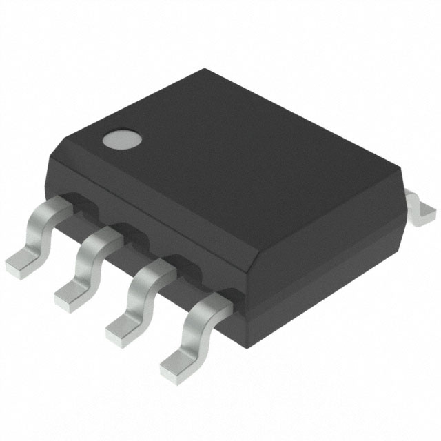


 工商网监
湘ICP备2023018690号
工商网监
湘ICP备2023018690号
