AT24CS04/AT24CS08
I²C-Compatible (Two-Wire) Serial EEPROM with a Unique,
Factory-Programmed 128-Bit Serial Number
4‑Kbit (512 x 8), 8‑Kbit (1,024 x 8)
Features
•
•
•
•
•
•
•
•
•
•
•
•
•
•
•
•
Low-Voltage Operation:
– VCC = 1.7V to 5.5V
Internally Organized as 512 x 8 (4K) or 1,024 x 8 (8K)
128-Bit Unique Factory-Programmed Serial Number
– Permanent read-only value
– Unique across entire CS Series of Serial EEPROMs
Industrial Temperature Range: -40°C to +85°C
I2C-Compatible (Two-Wire) Serial Interface:
– 100 kHz Standard Mode, 1.7V to 5.5V
– 400 kHz Fast Mode, 1.7V to 5.5V
– 1 MHz Fast Mode Plus (FM+), 2.5V to 5.5V
Schmitt Triggers, Filtered Inputs for Noise Suppression
Bidirectional Data Transfer Protocol
Write-Protect Pin for Full Array Hardware Data Protection
Ultra Low Active Current (3 mA maximum) and Standby Current (6 μA maximum)
16-Byte Page Write Mode:
– Partial page writes allowed
Random and Sequential Read Modes
Self-Timed Write Cycle within 5 ms Maximum
ESD Protection > 4,000V
High Reliability:
– Endurance: 1,000,000 write cycles
– Data retention: 100 years
Green Package Options (Lead-free/Halide-free/RoHS compliant)
Die Sale Options: Wafer Form and Tape and Reel Available
Packages
•
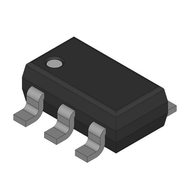
8-Lead SOIC, 8-Lead TSSOP, 8-Pad UDFN and 5-Lead SOT23
© 2020 Microchip Technology Inc.
Datasheet
DS20006350A-page 1
�AT24CS04/AT24CS08
Table of Contents
Features......................................................................................................................................................... 1
Packages........................................................................................................................................................1
1.
Package Types (not to scale)..................................................................................................................4
2.
Pin Descriptions...................................................................................................................................... 5
2.1.
2.2.
2.3.
2.4.
2.5.
2.6.
3.
Description.............................................................................................................................................. 7
3.1.
3.2.
4.
Device Addressing..................................................................................................................... 16
Write Operations................................................................................................................................... 19
7.1.
7.2.
7.3.
7.4.
7.5.
8.
Clock and Data Transition Requirements...................................................................................13
Start and Stop Conditions.......................................................................................................... 13
Acknowledge and No-Acknowledge...........................................................................................14
Standby Mode............................................................................................................................ 14
Software Reset...........................................................................................................................14
Memory Organization............................................................................................................................16
6.1.
7.
Absolute Maximum Ratings..........................................................................................................9
DC and AC Operating Range.......................................................................................................9
DC Characteristics....................................................................................................................... 9
AC Characteristics......................................................................................................................10
Electrical Specifications..............................................................................................................11
Device Operation and Communication................................................................................................. 13
5.1.
5.2.
5.3.
5.4.
5.5.
6.
System Configuration Using Two-Wire Serial EEPROMs ........................................................... 7
Block Diagram.............................................................................................................................. 8
Electrical Characteristics.........................................................................................................................9
4.1.
4.2.
4.3.
4.4.
4.5.
5.
Device Address Inputs (A1, A2)................................................................................................... 5
Ground......................................................................................................................................... 5
Serial Data (SDA).........................................................................................................................5
Serial Clock (SCL)........................................................................................................................5
Write-Protect (WP)....................................................................................................................... 6
Device Power Supply (VCC)......................................................................................................... 6
Byte Write...................................................................................................................................19
Page Write..................................................................................................................................19
Acknowledge Polling.................................................................................................................. 20
Write Cycle Timing..................................................................................................................... 20
Write Protection..........................................................................................................................21
Read Operations................................................................................................................................... 22
8.1.
8.2.
8.3.
8.4.
Current Address Read................................................................................................................22
Random Read............................................................................................................................ 22
Sequential Read.........................................................................................................................23
Serial Number Read...................................................................................................................24
© 2020 Microchip Technology Inc.
Datasheet
DS20006350A-page 2
�AT24CS04/AT24CS08
9.
Device Default Condition from Microchip.............................................................................................. 25
10. Packaging Information.......................................................................................................................... 26
10.1. Package Marking Information.....................................................................................................26
11. Revision History.................................................................................................................................... 38
The Microchip Website.................................................................................................................................39
Product Change Notification Service............................................................................................................39
Customer Support........................................................................................................................................ 39
Product Identification System.......................................................................................................................40
Microchip Devices Code Protection Feature................................................................................................ 40
Legal Notice................................................................................................................................................. 41
Trademarks.................................................................................................................................................. 41
Quality Management System....................................................................................................................... 42
Worldwide Sales and Service.......................................................................................................................43
© 2020 Microchip Technology Inc.
Datasheet
DS20006350A-page 3
�AT24CS04/AT24CS08
Package Types (not to scale)
1.
Package Types (not to scale)
8-lead SOIC/TSSOP
(Top View)
5-lead SOT23(2)
(Top View)
NC
1
8
Vcc
A1(1)/NC
2
7
WP
SCL
1
A2
3
6
SCL
GND
2
GND
4
5
SDA
SDA
3
5
WP
4
Vcc
8-pad UDFN
(Top View)
NC
1
8
Vcc
A1(1)/NC
2
7
WP
A2
3
6
SCL
GND
4
5
SDA
Note:
1. This pin is device address input (A1) pin on the AT24CS04 and is a NC or no connect on the AT24CS08. Refer
to Pin Description for additional details.
2. Refer to Device Addressing for details about addressing the SOT23 version of the device.
© 2020 Microchip Technology Inc.
Datasheet
DS20006350A-page 4
�AT24CS04/AT24CS08
Pin Descriptions
2.
Pin Descriptions
The descriptions of the pins are listed in Table 2-1.
Table 2-1. Pin Function Table
Name
NC
A1(2,3)/NC
A2(2)
GND
SDA
SCL
WP(2)
VCC
8-Lead SOIC 8-Lead TSSOP 8-Pad UDFN(1) 5-Lead SOT23
Function
1
1
1
-
No Connect
2
2
2
-
Device Address Input/ No
Connect
3
3
3
-
Device Address Input
4
4
4
2
Ground
5
5
5
3
Serial Data
6
6
6
1
Serial Clock
7
7
7
5
Write-Protect
8
8
8
4
Device Power Supply
Note:
1. The exposed pad on this package can be connected to GND or left floating.
2. If the A1, A2 or WP pins are not driven, they are internally pulled down to GND. In order to operate in a wide
variety of application environments, the pull-down mechanism is intentionally designed to be somewhat strong.
Once these pins are biased above the CMOS input buffer’s trip point (~0.5 x VCC), the pull‑down mechanism
disengages. Microchip recommends connecting these pins to a known state whenever possible.
3. This pin is device address input (A1) pin on the AT24CS04 and is a NC or no connect on the AT24CS08.
2.1
Device Address Inputs (A1, A2)
The A1 and A2 pins are device address inputs that are hard-wired (directly to GND or to VCC) for compatibility with
other two-wire Serial EEPROM devices. When the pins are hard-wired on the AT24CS04, as many as four devices
may be addressed on a single bus system. When the A2 pin is hard‑wired on the AT24CS08, as many as two
devices may be addressed on a single bus system. A device is selected when a corresponding hardware and
software match is true. If the pins are left floating, the A1 and A2 pins will be internally pulled down to GND. However,
due to capacitive coupling that may appear in customer applications, Microchip recommends always connecting the
address pins to a known state. When using a pull-up resistor, Microchip recommends using 10 kΩ or less.
2.2
Ground
The ground reference for the power supply. GND should be connected to the system ground.
2.3
Serial Data (SDA)
The SDA pin is an open-drain bidirectional input/output pin used to serially transfer data to and from the device. The
SDA pin must be pulled high using an external pull-up resistor (not to exceed 10 kΩ in value) and may be wire-ORed
with any number of other open-drain or open-collector pins from other devices on the same bus.
2.4
Serial Clock (SCL)
The SCL pin is used to provide a clock to the device and to control the flow of data to and from the device. Command
and input data present on the SDA pin is always latched in on the rising edge of SCL, while output data on the SDA
pin is clocked out on the falling edge of SCL. The SCL pin must either be forced high when the serial bus is idle or
pulled high using an external pull-up resistor.
© 2020 Microchip Technology Inc.
Datasheet
DS20006350A-page 5
�AT24CS04/AT24CS08
Pin Descriptions
2.5
Write-Protect (WP)
The write-protect input, when connected to GND, allows normal write operations. When the WP pin is connected
directly to VCC, all write operations to the protected memory are inhibited.
If the pin is left floating, the WP pin will be internally pulled down to GND. However, due to capacitive coupling that
may appear in customer applications, Microchip recommends always connecting the WP pin to a known state. When
using a pull‑up resistor, Microchip recommends using 10 kΩ or less.
Table 2-2. Write-Protect
2.6
WP Pin Status
Part of the Array Protected
At VCC
Full Array
At GND
Normal Write Operations
Device Power Supply (VCC)
The Device Power Supply (VCC) pin is used to supply the source voltage to the device. Operations at invalid VCC
voltages may produce spurious results and should not be attempted.
© 2020 Microchip Technology Inc.
Datasheet
DS20006350A-page 6
�AT24CS04/AT24CS08
Description
3.
Description
The AT24CS04/AT24CS08 provides 4,096/8,192 bits of Serial Electrically Erasable and Programmable Read-Only
Memory (EEPROM) organized as 512/1,024 words of 8 bits each. The device’s cascading feature allows up to four
devices (AT24CS04) or two devices (AT24CS08) to share a common two-wire bus. These devices are optimized for
use in many industrial and commercial applications where low‑power and low‑voltage operations are essential. The
devices are available in space-saving 8-lead SOIC, 8-lead TSSOP, 8-pad UDFN and 5-lead SOT23 packages. All
packages operate from 1.7V to 5.5V.
The AT24CS04/AT24CS08 provides the additional feature of a factory programmed, ensured unique 128‑bit serial
number, while maintaining all of the traditional features available in the 4‑Kbit and 8‑Kbit Serial EEPROMs. The time
consuming step of performing and ensuring true serialization of product on a manufacturing line can be removed from
the production flow by employing the CS Series Serial EEPROM. The 128‑bit serial number is programmed and
permanently locked from future writing during the Microchip production process. Further, this 128‑bit location does
not consume any of the user read/write area of the 4‑Kbit and 8‑Kbit Serial EEPROMs. The uniqueness of the serial
number is ensured across the entire CS Series of Serial EEPROMs, regardless of the size of the memory array or the
type of interface protocol. This means that as an application’s needs for memory size or interface protocol evolve in
future generations, any previously deployed serial number from any Microchip CS Series Serial EEPROM part will
remain valid.
3.1
System Configuration Using Two-Wire Serial EEPROMs
VCC
RPUP(max) =
tR(max)
0.8473 x CL
V - VOL(max)
RPUP(min) = CC
IOL
VCC
SCL
SDA
WP
I2C Bus Master:
Microcontroller
NC
A1
A2
GND
VCC
Slave 0 WP
AT24CSXX SDA
GND
SCL
NC
A1
A2
VCC
Slave 1 WP
AT24CSXX SDA
GND
SCL
NC
A1
A2
VCC
Slave 3 WP
AT24CSXX SDA
GND
SCL
Note: Only two devices can be connected when using the AT24CS08.
© 2020 Microchip Technology Inc.
Datasheet
DS20006350A-page 7
�AT24CS04/AT24CS08
Description
Block Diagram
Hardware
Address
Comparator
Memory
System Control
Module
Power-on
Reset
Generator
VCC
High Voltage
Generation Circuit
A1(1)
Row Decoder
3.2
EEPROM Array
1 page
128-bit Serial Number
A2
Write
Protection
Control
Address Register
and Counter
Column Decoder
SCL
Data Register
DOUT
Data & ACK
Input/Output Control
GND
WP
DIN
Start
Stop
Detector
SDA
Note:
1. The A1 pin is not available on the AT24CS08.
© 2020 Microchip Technology Inc.
Datasheet
DS20006350A-page 8
�AT24CS04/AT24CS08
Electrical Characteristics
4.
Electrical Characteristics
4.1
Absolute Maximum Ratings
Temperature under bias
-55°C to +125°C
Storage temperature
-65°C to +150°C
VCC
6.25V
Voltage on any pin with respect to ground
-1.0V to +7.0V
DC output current
5.0 mA
ESD protection
>4 kV
Note: Stresses above those listed under “Absolute Maximum Ratings” may cause permanent damage to the device.
This is a stress rating only and functional operation of the device at these or any other conditions above those
indicated in the operation listings of this specification is not implied. Exposure to absolute maximum rating conditions
for extended periods may affect device reliability.
4.2
DC and AC Operating Range
Table 4-1. DC and AC Operating Range
AT24CS04/AT24CS08
4.3
Operating Temperature (Case)
Industrial Temperature Range
-40°C to +85°C
VCC Power Supply
Low-Voltage Grade
1.7V to 5.5V
DC Characteristics
Table 4-2. DC Characteristics
Symbol
Minimum
Typical(1)
Maximum
Units
Supply
Voltage
VCC
1.7
—
5.5
V
Supply
Current
ICC1
—
0.4
1.0
mA
VCC = 5.0V, Read at 400 kHz
Supply
Current
ICC2
—
2.0
3.0
mA
VCC = 5.0V, Write at 400 kHz
Standby
Current
ISB
—
—
1.0
μA
VCC = 1.7V, VIN = VCC or GND
—
—
6.0
μA
VCC = 5.5V, VIN = VCC or GND
Input Leakage
Current
ILI
—
0.10
3.0
μA
VIN = VCC or GND
Output
Leakage
Current
ILO
—
0.05
3.0
μA
VOUT = VCC or GND
Input Low
Level
VIL
-0.6
—
VCC x 0.3
V
Note 2
Parameter
© 2020 Microchip Technology Inc.
Datasheet
Test Conditions
DS20006350A-page 9
�AT24CS04/AT24CS08
Electrical Characteristics
...........continued
Symbol
Minimum
Typical(1)
Maximum
Units
Input High
Level
VIH
VCC x 0.7
—
VCC + 0.5
V
Note 2
Output Low
Level
VOL1
—
—
0.2
V
VCC = 1.7V, IOL = 0.15 mA
Output Low
Level
VOL2
—
—
0.4
V
VCC = 3.0V, IOL = 2.1 mA
Parameter
Test Conditions
Note:
1.
2.
4.4
Typical values characterized at TA = +25°C unless otherwise noted.
This parameter is characterized but is not 100% tested in production.
AC Characteristics
Table 4-3. AC Characteristics(1)
Parameter
Symbol
fSCL
tLOW
tHIGH
tI
Fast Mode
VCC = 1.7V to 2.5V
Min.
Max.
—
400
1,200
—
600
—
—
100
Fast Mode Plus
VCC = 2.5V to 5.5V
Min.
Max.
—
1000
500
—
400
—
—
50
Clock Frequency, SCL
Clock Pulse Width Low
Clock Pulse Width High
Input Filter Spike
Suppression
Clock Low to Data Out Valid
Bus Free Time between
Stop and Start
Start Hold Time
Start Set-up Time
Data In Hold Time
Data In Set-up Time
Inputs Rise Time(2)
Inputs Fall Time(2)
Stop Set-up Time
Data Out Hold Time
Write Cycle Time
Units
tAA
tBUF
100
1,300
900
—
50
500
450
—
ns
ns
tHD.STA
tSU.STA
tHD.DAT
tSU.DAT
tR
tF
tSU.STO
tDH
tWR
600
600
0
100
—
—
600
50
—
—
—
—
—
300
300
—
—
5
250
250
0
100
—
—
250
50
—
—
—
—
—
300
100
—
—
5
ns
ns
ns
ns
ns
ns
ns
ns
ms
kHz
ns
ns
ns
Note:
1. AC measurement conditions:
– CL: 100 pF
– RPUP (SDA bus line pull-up resistor to VCC): 1.3 kΩ (1000 kHz), 4 kΩ (400 kHz), 10 kΩ (100 kHz)
– Input rise and fall times: ≤50 ns
– Input and output timing reference voltages: 0.5 x VCC
2. These parameters are determined through product characterization and are not 100% tested in production.
© 2020 Microchip Technology Inc.
Datasheet
DS20006350A-page 10
�AT24CS04/AT24CS08
Electrical Characteristics
Figure 4-1. Bus Timing
tF
tHIGH
tR
tLOW
SCL
tSU.STA
tHD.STA
tHD.DAT
tSU.DAT
tSU.STO
SDA In
tBUF
tAA
tDH
SDA Out
4.5
4.5.1
Electrical Specifications
Power-Up Requirements and Reset Behavior
During a power-up sequence, the VCC supplied to the AT24CS04/AT24CS08 should monotonically rise from GND to
the minimum VCC level, as specified in Table 4-1, with a slew rate no faster than 0.1 V/µs.
4.5.1.1
Device Reset
To prevent inadvertent write operations or any other spurious events from occurring during a power-up sequence, the
AT24CS04/AT24CS08 includes a Power-on Reset (POR) circuit. Upon power-up, the device will not respond to any
commands until the VCC level crosses the internal voltage threshold (VPOR) that brings the device out of Reset and
into Standby mode.
The system designer must ensure the instructions are not sent to the device until the VCC supply has reached a
stable value greater than or equal to the minimum VCC level. Additionally, once the VCC is greater than or equal to the
minimum VCC level, the bus master must wait at least tPUP before sending the first command to the device. See Table
4-4 for the values associated with these power-up parameters.
Table 4-4. Power-up Conditions(1)
Symbol
Parameter
tPUP
Time required after VCC is stable before the device can accept commands
VPOR
Power-on Reset Threshold Voltage
tPOFF
Minimum time at VCC = 0V between power cycles
Min.
Max.
Units
100
-
µs
-
1.5
V
500
-
ms
Note:
1. These parameters are characterized but they are not 100% tested in production.
If an event occurs in the system where the VCC level supplied to the AT24CS04/AT24CS08 drops below the
maximum VPOR level specified, it is recommended that a full power cycle sequence be performed by first driving the
VCC pin to GND, waiting at least the minimum tPOFF time and then performing a new power-up sequence in
compliance with the requirements defined in this section.
© 2020 Microchip Technology Inc.
Datasheet
DS20006350A-page 11
�AT24CS04/AT24CS08
Electrical Characteristics
4.5.2
Pin Capacitance
Table 4-5. Pin Capacitance(1)
Symbol
Test Condition
Max.
Units
Conditions
CI/O
Input/Output Capacitance (SDA)
8
pF
VI/O = 0V
CIN
Input Capacitance (A1, A2 and SCL)
6
pF
VIN = 0V
Note:
1. This parameter is characterized but is not 100% tested in production.
4.5.3
EEPROM Cell Performance Characteristics
Table 4-6. EEPROM Cell Performance Characteristics
Operation
Test Condition
Write Endurance(1)
TA = 25°C, VCC = 3.3V,
Page Write mode
Data Retention(1)
TA = 55°C
Min.
Max.
Units
1,000,000
—
Write Cycles
100
—
Years
Note:
1. Performance is determined through characterization and the qualification process.
© 2020 Microchip Technology Inc.
Datasheet
DS20006350A-page 12
�AT24CS04/AT24CS08
Device Operation and Communication
5.
Device Operation and Communication
The AT24CS04/AT24CS08 operates as a slave device and utilizes a simple I2C-compatible two-wire digital serial
interface to communicate with a host controller, commonly referred to as the bus master. The master initiates and
controls all read and write operations to the slave devices on the serial bus, and both the master and the slave
devices can transmit and receive data on the bus.
The serial interface is comprised of just two signal lines: Serial Clock (SCL) and Serial Data (SDA). The SCL pin is
used to receive the clock signal from the master, while the bidirectional SDA pin is used to receive command and
data information from the master as well as to send data back to the master. Data is always latched into the
AT24CS04/AT24CS08 on the rising edge of SCL and always output from the device on the falling edge of SCL. Both
the SCL and SDA pins incorporate integrated spike suppression filters and Schmitt Triggers to minimize the effects of
input spikes and bus noise.
All command and data information is transferred with the Most Significant bit (MSb) first. During bus communication,
one data bit is transmitted every clock cycle, and after eight bits (one byte) of data have been transferred, the
receiving device must respond with either an Acknowledge (ACK) or a No-Acknowledge (NACK) response bit during
a ninth clock cycle (ACK/NACK clock cycle) generated by the master. Therefore, nine clock cycles are required for
every one byte of data transferred. There are no unused clock cycles during any read or write operation, so there
must not be any interruptions or breaks in the data stream during each data byte transfer and ACK or NACK clock
cycle.
During data transfers, data on the SDA pin must only change while SCL is low, and the data must remain stable while
SCL is high. If data on the SDA pin changes while SCL is high, then either a Start or a Stop condition will occur. Start
and Stop conditions are used to initiate and end all serial bus communication between the master and the slave
devices. The number of data bytes transferred between a Start and a Stop condition is not limited and is determined
by the master. In order for the serial bus to be idle, both the SCL and SDA pins must be in the logic high state at the
same time.
5.1
Clock and Data Transition Requirements
The SDA pin is an open-drain terminal and therefore must be pulled high with an external pull‑up resistor. SCL is an
input pin that can either be driven high or pulled high using an external pull‑up resistor. Data on the SDA pin may
change only during SCL low time periods. Data changes during SCL high periods will indicate a Start or Stop
condition as defined below. The relationship of the AC timing parameters with respect to SCL and SDA for the
AT24CS04/AT24CS08 are shown in the timing waveform in Figure 4-1. The AC timing characteristics and
specifications are outlined in AC Characteristics.
5.2
Start and Stop Conditions
5.2.1
Start Condition
A Start condition occurs when there is a high-to-low transition on the SDA pin while the SCL pin is at a stable logic ‘1’
state and will bring the device out of Standby mode. The master uses a Start condition to initiate any data transfer
sequence; therefore, every command must begin with a Start condition. The device will continuously monitor the SDA
and SCL pins for a Start condition but will not respond unless one is detected. Refer to Figure 5-1 for more details.
5.2.2
Stop Condition
A Stop condition occurs when there is a low-to-high transition on the SDA pin while the SCL pin is stable in the logic
‘1’ state.
The master can use the Stop condition to end a data transfer sequence with the AT24CS04/AT24CS08, which will
subsequently return to Standby mode. The master can also utilize a repeated Start condition instead of a Stop
condition to end the current data transfer if the master will perform another operation. Refer to Figure 5-1 for more
details.
© 2020 Microchip Technology Inc.
Datasheet
DS20006350A-page 13
�AT24CS04/AT24CS08
Device Operation and Communication
5.3
Acknowledge and No-Acknowledge
After every byte of data is received, the receiving device must confirm to the transmitting device that it has
successfully received the data byte by responding with what is known as an Acknowledge (ACK).
An ACK is accomplished by the transmitting device first releasing the SDA line at the falling edge of the eighth clock
cycle followed by the receiving device responding with a logic ‘0’ during the entire high period of the ninth clock cycle.
When the AT24CS04/AT24CS08 is transmitting data to the master, the master can indicate that it is done receiving
data and wants to end the operation by sending a logic ‘1’ response to the AT24CS04/AT24CS08 instead of an ACK
response during the ninth clock cycle. This is known as a No-Acknowledge (NACK) and is accomplished by the
master sending a logic ‘1’ during the ninth clock cycle, at which point the AT24CS04/AT24CS08 will release the SDA
line so the master can then generate a Stop condition.
The transmitting device, which can be the bus master or the Serial EEPROM, must release the SDA line at the falling
edge of the eighth clock cycle to allow the receiving device to drive the SDA line to a logic ‘0’ to ACK the previous 8bit word. The receiving device must release the SDA line at the end of the ninth clock cycle to allow the transmitter to
continue sending new data. A timing diagram has been provided in Figure 5-1 to better illustrate these requirements.
Figure 5-1. Start Condition, Data Transitions, Stop Condition and Acknowledge
SCL
SDA
Must Be
Stable
SDA
Must Be
Stable
1
2
Acknowledge Window
8
9
SDA
Start
Condition
5.4
Acknowledge
Valid
SDA
Change
Allowed
SDA
Change
Allowed
The transmitting device (Master or Slave)
must release the SDA line at this point to allow
the receiving device (Master or Slave) to drive the
SDA line low to ACK the previous 8-bit word.
Stop
Condition
The receiver (Master or Slave)
must release the SDA line at
this point to allow the transmitter
to continue sending new data.
Standby Mode
The AT24CS04/AT24CS08 features a low-power Standby mode that is enabled when any one of the following
occurs:
•
•
•
5.5
A valid power-up sequence is performed (see Power-Up Requirements and Reset Behavior).
A Stop condition is received by the device unless it initiates an internal write cycle (see Write Operations).
At the completion of an internal write cycle (see Write Operations).
Software Reset
After an interruption in protocol, power loss or system Reset, any two‑wire device can be protocol reset by clocking
SCL until SDA is released by the EEPROM and goes high. The number of clock cycles until SDA is released by the
EEPROM will vary. The software Reset sequence should not take more than nine dummy clock cycles. Once the
software Reset sequence is complete, new protocol can be sent to the device by sending a Start condition followed
by the protocol. Refer to Figure 5-2 for an illustration.
© 2020 Microchip Technology Inc.
Datasheet
DS20006350A-page 14
�AT24CS04/AT24CS08
Device Operation and Communication
Figure 5-2. Software Reset
Dummy Clock Cycles
SCL
1
2
3
8
SDA Released
by EEPROM
9
Device is
Software Reset
SDA
In the event that the device is still non-responsive or remains active on the SDA bus, a power cycle must be used to
reset the device (see Power-Up Requirements and Reset Behavior).
© 2020 Microchip Technology Inc.
Datasheet
DS20006350A-page 15
�AT24CS04/AT24CS08
Memory Organization
6.
Memory Organization
The AT24CS04 is internally organized as 32 pages of 16 bytes each. The AT24CS08 is internally organized as 64
pages of 16 bytes each.
6.1
6.1.1
Device Addressing
AT24CS04 Device Addressing
Accessing the device requires an 8-bit device address byte following a Start condition to enable the device for a read
or write operation. Since multiple slave devices can reside on the serial bus, each slave device must have its own
unique address so the master can access each device independently.
The Most Significant four bits of the device address byte is referred to as the device type identifier. The device type
identifier ‘1010’ (Ah) is required in bits 7 through 4 of the device address byte (see Table 6‑1).
The AT24CS04 utilizes a separate memory block containing a factory programmed 128-bit serial number. Access to
this memory location is similar to the EERPOM region with the exception that the device type identifier is set to ‘1011’
(Bh) in bits 7 through 4 of the device address byte (see Table 6‑1).
Following the 4-bit device type identifier are the hardware slave address bits, A2 and A1. These bits can be used to
expand the address space by allowing up to four Serial EEPROM devices on the same bus. The A2 and A1 values
must correlate with the voltage level on the corresponding hardwired device address input pins A1 and A2. The A1
and A2 pins use an internal proprietary circuit that automatically biases the pin to a logic ‘0’ state if the pin is allowed
to float. In order to operate in a wide variety of application environments, the pull‑down mechanism is intentionally
designed to be somewhat strong. Once these pins are biased above the CMOS input buffer’s trip point (~0.5 x VCC),
the pull-down mechanism disengages. Microchip recommends connecting the A1 and A2 pins to a known state
whenever possible.
When using the SOT23 package, the A1 and A2 pins are not accessible and are left floating. The previously
mentioned automatic pull‑down circuit will set these pins to a logic ‘0’ state. As a result, to properly communicate with
the device in the SOT23 package, the A2 and A1 software bits must always be set to logic ‘0’ for any operation.
Following the A2 and A1 hardware slave address bits is bit A8 (bit 1 of the device address byte), which is the Most
Significant bit of the memory array word address. Refer to Table 6‑1 to review the bit position.
The eighth bit (bit 0) of the device address byte is the Read/Write Select bit. A read operation is initiated if this bit is
high and a write operation is initiated if this bit is low.
Upon the successful comparison of the device address byte, the AT24CS04 will return an ACK. If a valid comparison
is not made, the device will NACK.
Table 6-1. AT24CS04 Device Address Byte
Access Area
Device Type Identifier
Bit 7 Bit 6 Bit 5 Bit 4
Hardware Slave Address
Bits(1)
Most Significant Bit of
the Word Address
R/W Select
Bit 3
Bit 2
Bit 1
Bit 0
EEPROM
1
0
1
0
A2
A1
A8
R/W
Serial Number
1
0
1
1
A2
A1
0
R/W
Note:
1. The hardware slave address bits must be set to logic ‘0’ when using the SOT23 package.
For all operations except the current address read, a word address byte must be transmitted to the device
immediately following the device address byte. The word address byte consists of the remaining eight bits of the 9-bit
memory array word address, and is used to specify which byte location in the EEPROM to start reading or writing.
Refer to Table 6-2 to review these bit positions.
© 2020 Microchip Technology Inc.
Datasheet
DS20006350A-page 16
�AT24CS04/AT24CS08
Memory Organization
Table 6-2. AT24CS04 Word Address Byte
Access Area
EEPROM
Serial Number
6.1.2
Bit 7
Bit 6
Bit 5
Bit 4
Bit 3
Bit 2
Bit 1
Bit 0
A7
A6
A5
A4
A3
A2
A1
A0
1
0
X
X
X
X
X
X
AT24CS08 Device Addressing
Accessing the device requires an 8-bit device address byte following a Start condition to enable the device for a read
or write operation. Since multiple slave devices can reside on the serial bus, each slave device must have its own
unique address so the master can access each device independently.
The Most Significant four bits of the device address byte is referred to as the device type identifier. The device type
identifier ‘1010’ (Ah) is required in bits 7 through 4 of the device address byte (see Table 6‑3).
The AT24CS08 utilizes a separate memory block containing a factory programmed 128-bit serial number. Access to
this memory location is similar to the EERPOM region with the exception that the device type identifier is set to ‘1011’
(Bh) in bits 7 through 4 of the device address byte (see Table 6‑3).
Following the 4-bit device type identifier is the hardware slave address bit, A2. This bit can be used to expand the
address space by allowing up to two Serial EEPROM devices on the same bus. The A2 value must correlate with the
voltage level on the corresponding hardwired device address input pin A2. The A2 pin uses an internal proprietary
circuit that automatically biases it to a logic ‘0’ state if the pin is allowed to float. In order to operate in a wide variety
of application environments, the pull‑down mechanism is intentionally designed to be somewhat strong. Once the pin
is biased above the CMOS input buffer’s trip point (~0.5 x VCC), the pull-down mechanism disengages. Microchip
recommends connecting the A2 pin to a known state whenever possible.
When using the SOT23 package, the A2 pin is not accessible and is left floating. The previously mentioned automatic
pull‑down circuit will set this pin to a logic ‘0’ state. As a result, to properly communicate with the device in the SOT23
package, the A2 software bit must always be set to logic ‘0’ for any operation.
Following the A2 hardware slave address bit are bits A9 and A8 (bit 2 and bit 1 of the device address byte), which are
the two Most Significant bits of the memory array word address. Refer to Table 6‑3 to review these bit positions.
The eighth bit (bit 0) of the device address byte is the Read/Write Select bit. A read operation is initiated if this bit is
high and a write operation is initiated if this bit is low.
Upon the successful comparison of the device address byte, the AT24CS08 will return an ACK. If a valid comparison
is not made, the device will NACK.
Table 6-3. AT24CS08 Device Address Byte
Access Area
Device Type Identifier
Hardware Slave
Address Bit(1)
Most Significant Bits of the Word
Address
R/W Select
Bit 7 Bit 6 Bit 5 Bit 4
Bit 3
Bit 2
Bit 1
Bit 0
EEPROM
1
0
1
0
A2
A9
A8
R/W
Serial Number
1
0
1
1
A2
0
0
R/W
Note:
1. The hardware slave address bit must be set to logic ‘0’ when using the SOT23 package.
For all operations except the current address read, a word address byte must be transmitted to the device
immediately following the device address byte. The word address byte consists of the remaining eight bits of the 10bit memory array word address, and is used to specify which byte location in the EEPROM to start reading or writing.
Refer to Table 6-4 to review these bit positions.
Table 6-4. AT24CS08 Word Address Byte
Access Area
EEPROM
© 2020 Microchip Technology Inc.
Bit 7
Bit 6
Bit 5
Bit 4
Bit 3
Bit 2
Bit 1
Bit 0
A7
A6
A5
A4
A3
A2
A1
A0
Datasheet
DS20006350A-page 17
�AT24CS04/AT24CS08
Memory Organization
...........continued
Access Area
Bit 7
Bit 6
Bit 5
Bit 4
Bit 3
Bit 2
Bit 1
Bit 0
Serial Number
1
0
X
X
X
X
X
X
© 2020 Microchip Technology Inc.
Datasheet
DS20006350A-page 18
�AT24CS04/AT24CS08
Write Operations
7.
Write Operations
All write operations for the AT24CS04/AT24CS08 begin with the master sending a Start condition, followed by a
device address byte with the R/W bit set to logic ‘0’, and then by the word address byte. The data value(s) to be
written to the device immediately follow the word address byte.
7.1
Byte Write
The AT24CS04/AT24CS08 supports the writing of a single 8-bit byte. Selecting a data word in the AT24CS04
requires a 9-bit word address and selecting a data word in the AT24CS08 requires a 10-bit word address.
Upon receipt of the proper device address and the word address bytes, the EEPROM will send an Acknowledge. The
device will then be ready to receive the 8-bit data word. Following receipt of the 8‑bit data word, the EEPROM will
respond with an ACK. The addressing device, such as a bus master, must then terminate the write operation with a
Stop condition. At that time, the EEPROM will enter an internally self-timed write cycle, which will be completed within
tWR, while the data word is being programmed into the nonvolatile EEPROM. All inputs are disabled during this write
cycle, and the EEPROM will not respond until the write is complete.
Figure 7-1. Byte Write
1
SCL
2
3
4
5
6
7
8
9
1
2
Device Address Byte
SDA
1
MSb
0
1
0
A2
Start
by
Master
(1)
@
3
4
5
6
7
8
9
1
2
3
0
0
A7
A6
A5
A4
A3
A2
5
6
7
8
9
D2
D1
D0
0
Data Word
Word Address Byte
A8
4
A1
MSb
ACK
from
Slave
A0
0
ACK
from
Slave
D7
MSb
D6
D5
D4
D3
ACK
from
Slave
Stop
by
Master
Note:
1. For the AT24CS04, the @ indicates the A1 hardware slave address bit. For the AT24CS08, the @ indicates the
A9 word address bit.
7.2
Page Write
A page write operation allows up to 16 bytes to be written in the same write cycle, provided all bytes are in the same
row of the memory array (where address bits A8/A9 through A4 are the same). Partial page writes of less than 16
bytes are also allowed.
A page write is initiated the same way as a byte write, but the bus master does not send a Stop condition after the
first data word is clocked in. Instead, after the EEPROM acknowledges receipt of the first data word, the bus master
can transmit up to fifteen additional data words. The EEPROM will respond with an ACK after each data word is
received. Once all data to be written has been sent to the device, the bus master must issue a Stop condition (see
Figure 7-2) at which time the internally self-timed write cycle will begin.
The lower four bits of the word address are internally incremented following the receipt of each data word. The higher
order address bits are not incremented and retain the memory page row location. Page write operations are limited to
writing bytes within a single physical page, regardless of the number of bytes actually being written. When the
incremented word address reaches the page boundary, the address counter will rollover to the beginning of the same
page. Nevertheless, creating a rollover event should be avoided as previously loaded data in the page could become
unintentionally altered.
© 2020 Microchip Technology Inc.
Datasheet
DS20006350A-page 19
�AT24CS04/AT24CS08
Write Operations
Figure 7-2. Page Write
1
SCL
2
3
4
5
6
7
8
9
1
2
3
Device Address Byte
SDA
1
MSb
0
1
A2
0
(1)
@
4
5
6
7
8
9
A1
A0
0
Word Address Byte
A8
Start
by
Master
0
A7
0
A6
A5
A4
A3
A2
MSb
ACK
from
Slave
1
2
ACK
from
Slave
3
4
5
6
7
8
9
Data Word (n)
D7
D6
D5
D4
D3
1
2
3
4
5
6
7
8
9
Data Word (n+x), max of 16 without rollover
D2
D1
D0
0
MSb
D7
D6
D5
D4
D3
D2
D1
D0
0
MSb
ACK
from
Slave
ACK
from
Slave
Stop
by
Master
Note:
1. For the AT24CS04, the @ indicates the A1 hardware slave address bit. For the AT24CS08, the @ indicates the
A9 word address bit.
7.3
Acknowledge Polling
An Acknowledge Polling routine can be implemented to optimize time-sensitive applications that would prefer not to
wait the fixed maximum write cycle time (tWR). This method allows the application to know immediately when the
Serial EEPROM write cycle has completed, so a subsequent operation can be started.
Once the internally self-timed write cycle has started, an Acknowledge Polling routine can be initiated. This involves
repeatedly sending a Start condition followed by a valid device address byte with the R/W bit set at logic ‘0’. The
device will not respond with an ACK while the write cycle is ongoing. Once the internal write cycle has completed, the
EEPROM will respond with an ACK, allowing a new read or write operation to be immediately initiated. A flowchart
has been included below in Figure 7-3 to better illustrate this technique.
Figure 7-3. Acknowledge Polling Flowchart
Send any
Write
protocol.
Send
Stop
condition
to initiate the
Write cycle.
Send Start
condition followed
by a valid
Device Address
byte with R/W = 0.
Did
the device
ACK?
YES
Proceed to
next Read or
Write operation.
NO
7.4
Write Cycle Timing
The length of the self-timed write cycle (tWR) is defined as the amount of time from the Stop condition that begins the
internal write cycle to the Start condition of the first device address byte sent to the AT24CS04/AT24CS08 that it
subsequently responds to with an ACK. Figure 7-4 has been included to show this measurement. During the
internally self-timed write cycle, any attempts to read from or write to the memory array will not be processed.
© 2020 Microchip Technology Inc.
Datasheet
DS20006350A-page 20
�AT24CS04/AT24CS08
Write Operations
Figure 7-4. Write Cycle Timing
SCL
8
9
9
ACK
ACK
Data Word n
SDA
D0
tWR
Stop
Condition
7.5
Start
Condition
First Acknowledge from the device
to a valid device address sequence after
write cycle is initiated. The minimum tWR
can only be determined through
the use of an ACK Polling routine.
Stop
Condition
Write Protection
The AT24CS04/AT24CS08 utilizes a hardware data protection scheme that allows the user to write‑protect the entire
memory contents when the WP pin is at VCC (or a valid VIH). No write protection will be set if the WP pin is at GND or
left floating.
Table 7-1. AT24CS04/AT24CS08 Write-Protect Behavior
WP Pin Voltage
Part of the Array Protected
VCC
Full Array
GND
None - Write Protection Not Enabled
The status of the WP pin is sampled at the Stop condition for every byte write or page write operation prior to the start
of an internally self‑timed write cycle. Changing the WP pin state after the Stop condition has been sent will not alter
or interrupt the execution of the write cycle.
If an attempt is made to write to the device while the WP pin has been asserted, the device will acknowledge the
device address, word address and data bytes, but no write cycle will occur when the Stop condition is issued. The
device will immediately be ready to accept a new read or write command.
© 2020 Microchip Technology Inc.
Datasheet
DS20006350A-page 21
�AT24CS04/AT24CS08
Read Operations
8.
Read Operations
Read operations are initiated the same way as write operations with the exception that the Read/Write Select bit in
the device address byte must be a logic ‘1’. There are four read operations:
•
•
•
•
Current Address Read
Random Address Read
Sequential Read
Serial Number Read
Note: The AT24CS04/AT24CS08 contains a single Address Pointer register, which is shared by both the EEPROM
and the serial number. As such, when changing from one region to the other, the first read operation in the new
region should begin with a dummy write sequence (i.e., a random read operation with the new region’s device
address and word address bytes) in order to ensure the Address Pointer is set to a known value. See Serial Number
Read for additional requirements on the serial number read.
8.1
Current Address Read
The internal data word address counter maintains the last address accessed during the last read or write operation,
incremented by one. This address stays valid between operations as long as the VCC is maintained to the part. The
address rollover during a read is from the last byte of the last page to the first byte of the first page of the memory.
A current address read operation will output data according to the location of the internal data word address counter.
This is initiated with a Start condition, followed by a valid device address byte with the R/W bit set to logic ‘1’. The
device will ACK this sequence and the current address data word is serially clocked out on the SDA line. All types of
read operations will be terminated if the bus master does not respond with an ACK (it NACKs) during the ninth clock
cycle. After the NACK response, the master may send a Stop condition to complete the protocol, or it can send a
Start condition to begin the next sequence.
Figure 8-1. Current Address Read
1
SCL
2
3
4
5
6
7
8
9
1
2
Device Address Byte
SDA
1
MSb
Start
by
Master
0
1
0
A2
@
(1)
3
4
5
6
7
8
9
D2
D1
D0
1
Data Word (n)
A8
1
0
D7
D6
MSb
ACK
from
Slave
D5
D4
D3
NACK
from
Master
Stop
by
Master
Note:
1. For the AT24CS04, the @ indicates the A1 hardware slave address bit. For the AT24CS08, the @ indicates the
A9 word address bit.
8.2
Random Read
A random read begins in the same way as a byte write operation does to load in a new data word address. This is
known as a “dummy write” sequence; however, the data byte and the Stop condition of the byte write must be omitted
to prevent the part from entering an internal write cycle. Once the device address and word address are clocked in
and acknowledged by the EEPROM, the bus master must generate another Start condition. The bus master now
initiates a current address read by sending a Start condition, followed by a valid device address byte with the R/W bit
set to logic ‘1’. In this second device address byte, the bit position usually reserved for the Most Significant bit of the
word address (bit 1 for AT24CS04 and bit 2 and 1 for AT24CS08) are “don’t care” bits since the address that will be
read from is determined only by what was sent in the dummy write portion of the sequence. The EEPROM will ACK
the device address and serially clock out the data word on the SDA line. All types of read operations will be
terminated if the bus master does not respond with an ACK (it NACKs) during the ninth clock cycle. After the NACK
response, the master may send a Stop condition to complete the protocol, or it can send a Start condition to begin
the next sequence.
© 2020 Microchip Technology Inc.
Datasheet
DS20006350A-page 22
�AT24CS04/AT24CS08
Read Operations
Figure 8-2. Random Read
1
SCL
2
3
4
5
6
7
8
9
1
2
3
Device Address Byte
SDA
1
0
MSb
1
(1)
A2
0
@
4
5
6
7
8
9
A1
A0
0
Word Address Byte
A8
0
A7
0
Start
by
Master
A6
A5
A4
A3
A2
MSb
ACK
from
Slave
ACK
from
Slave
Dummy Write
1
2
3
4
5
6
7
8
9
1
2
3
0
1
0
(1)
A2
@
5
6
7
8
9
D2
D1
D0
1
Data Word (n)
Device Address Byte
1
4
X
1
D7
0
MSb
D6
D5
D4
D3
MSb
Start
by
Master
ACK
from
Slave
NACK
from
Master
Stop
by
Master
Note:
1. For the AT24CS04, the @ indicates the A1 hardware slave address bit. For the AT24CS08, the @ indicates a
“don’t care” bit.
8.3
Sequential Read
Sequential reads are initiated by either a current address read or a random read. After the bus master receives a
data word, it responds with an Acknowledge. As long as the EEPROM receives an ACK, it will continue to increment
the word address and serially clock out sequential data words. When the maximum memory address is reached, the
data word address will rollover and the sequential read will continue from the beginning of the memory array. All
types of read operations will be terminated if the bus master does not respond with an ACK (it NACKs) during the
ninth clock cycle. After the NACK response, the master may send a Stop condition to complete the protocol, or it can
send a Start condition to begin the next sequence.
Figure 8-3. Sequential Read
1
SCL
2
3
4
5
6
7
8
9
1
2
3
Device Address Byte
SDA
1
0
MSb
1
(1)
A2
0
@
A8
1
D7
0
6
7
8
9
D6
D5
D4
D3
D2
D1
D0
0
MSb
ACK
from
Slave
2
3
4
5
6
7
8
9
1
2
Data Word (n+1)
D7
5
Data Word (n)
Start
by
Master
1
4
D6
D5
D4
D3
D2
MSb
ACK
from
Master
3
4
5
6
7
8
9
1
2
Data Word (n+2)
D1
D0
0
D7
D6
D5
D4
D3
D2
3
4
5
6
7
8
9
D1
D0
1
Data Word (n+x)
D1
MSb
ACK
from
Master
D0
0
ACK
from
Master
D7
MSb
D6
D5
D4
D3
D2
NACK
from
Master
Stop
by
Master
Note:
1. For the AT24CS04, the @ indicates the A1 hardware slave address bit. For the AT24CS08, the @ indicates the
A9 word address bit.
© 2020 Microchip Technology Inc.
Datasheet
DS20006350A-page 23
�AT24CS04/AT24CS08
Read Operations
8.4
Serial Number Read
Reading the serial number is similar to the sequential read sequence but requires use of the specific device Address
and word address bytes as specified in Table 6-1 and Table 6-2.
Note: The entire 128-bit value must be read from the starting address of the serial number block to ensure a unique
number.
Since the Address Pointer of the device is shared between the regular EEPROM array and the serial number block, a
dummy write sequence, as part of a random read or sequential read protocol, should be performed to ensure the
Address Pointer is set to a known value. Reading the serial number from a location other than the first address of the
block will not result in a unique serial number.
Additionally, the word address contains a ‘10’ sequence in bit A7 and A6 of the word address, regardless of the
intended address as depicted in Table 6-2. If a word address other than ‘10’ is used, then the device will output
undefined data.
Note: If the application desires to read the first byte of the serial number, the word address input would need to be
80h.
When the end of the 128-bit serial number is reached (16 bytes of data), continued reading of the extended memory
region will rollover back to the beginning of the 128-bit serial number. The serial number read operation is terminated
when the bus master does not respond with an ACK (it NACKs) during the ninth clock cycle. After the NACK
response, the master may send a Stop condition to complete the protocol, or it can send a Start condition to begin
the next sequence (see Figure 8-4).
Figure 8-4. Serial Number Read
SCL
1
2
3
4
5
6
7
8
9
1
2
Device Address Byte
SDA
1
MSb
0
1
1
A2
(1)
@
3
4
5
6
7
8
9
0
0
0
Word Address Byte
0
0
Start Condition
by Master
0
1
MSb
0
0
0
0
0
ACK
from Slave
ACK
from Slave
Dummy Write
1
2
3
4
5
6
7
8
9
1
2
Device Address Byte
1
0
1
1
A2
MSb
Start Condition
by Master
(1)
@
3
4
5
6
7
8
9
1
Serial Number Byte0
0
1
0
D7
D6
D5
D4
D3
D2
2
3
4
5
6
7
8
9
D1
D0
1
Serial Number Byte15
D1
MSb
D0
0
D7
D6
D5
D4
D3
D2
MSb
ACK
from Slave
ACK
from Master
Stop Condition
NACK
by Master
from Master
Note:
1. For the AT24CS04, the @ indicates the A1 hardware slave address bit. For the AT24CS08, the @ indicates a
logic ‘0’ bit.
© 2020 Microchip Technology Inc.
Datasheet
DS20006350A-page 24
�AT24CS04/AT24CS08
Device Default Condition from Microchip
9.
Device Default Condition from Microchip
The AT24CS04/AT24CS08 is delivered with the EEPROM array set to logic ‘1’, resulting in FFh data in all locations.
© 2020 Microchip Technology Inc.
Datasheet
DS20006350A-page 25
�AT24CS04/AT24CS08
Packaging Information
10.
Packaging Information
10.1
Package Marking Information
AT24CS04 and AT24CS08: Package Marking Information
8-lead TSSOP
8-lead SOIC
ATHYWW
## %CO
ATMLHYWW
## % CO
YYWWNNN
8-pad UDFN
YYWWNNN
5-lead SOT23
2.0 x 3.0 mm Body
##
H%
NNN
Note 1:
##%UYY
WWNNN
designates pin 1
Note 2: Package drawings are not to scale
Catalog Number Truncation
AT24CS04
Truncation Code ##: N4
AT24CS08
Truncation Code ##: N8
Date Codes
YY = Year
16: 2016
17: 2017
18: 2018
19: 2019
Voltages
20: 2020
21: 2021
22: 2022
23: 2023
Y = Year
6: 2016
7: 2017
8: 2018
9: 2019
0: 2020
1: 2021
2: 2022
3: 2023
WW = Work Week of Assembly
02: Week 2
04: Week 4
...
52: Week 52
Country of Origin
Device Grade
CO = Country of Origin
H or U: Industrial Grade
% = Minimum Voltage
M: 1.7V min
Atmel Truncation
AT: Atmel
ATM: Atmel
ATML: Atmel
Trace Code
NNN = Alphanumeric Trace Code (2 Characters for Small Packages)
© 2020 Microchip Technology Inc.
Datasheet
DS20006350A-page 26
�AT24CS04/AT24CS08
Packaging Information
8-Lead Plastic Small Outline (SN) - Narrow, 3.90 mm (.150 In.) Body [SOIC]
Note:
For the most current package drawings, please see the Microchip Packaging Specification located at
http://www.microchip.com/packaging
2X
0.10 C A–B
D
A
D
NOTE 5
N
E
2
E1
2
E1
E
NOTE 1
2
1
e
B
NX b
0.25
C A–B D
NOTE 5
TOP VIEW
0.10 C
C
A A2
SEATING
PLANE
8X
A1
SIDE VIEW
0.10 C
h
R0.13
h
R0.13
H
0.23
L
SEE VIEW C
(L1)
VIEW A–A
VIEW C
Microchip Technology Drawing No. C04-057-SN Rev D Sheet 1 of 2
© 2017 Microchip Technology Incorporated
© 2020 Microchip Technology Inc.
Datasheet
DS20006350A-page 27
�AT24CS04/AT24CS08
Packaging Information
8-Lead Plastic Small Outline (SN) - Narrow, 3.90 mm (.150 In.) Body [SOIC]
Note:
For the most current package drawings, please see the Microchip Packaging Specification located at
http://www.microchip.com/packaging
Units
Dimension Limits
Number of Pins
N
e
Pitch
Overall Height
A
Molded Package Thickness
A2
§
Standoff
A1
Overall Width
E
Molded Package Width
E1
Overall Length
D
Chamfer (Optional)
h
Foot Length
L
L1
Footprint
Foot Angle
c
Lead Thickness
b
Lead Width
Mold Draft Angle Top
Mold Draft Angle Bottom
MIN
1.25
0.10
0.25
0.40
0°
0.17
0.31
5°
5°
MILLIMETERS
NOM
8
1.27 BSC
6.00 BSC
3.90 BSC
4.90 BSC
1.04 REF
-
MAX
1.75
0.25
0.50
1.27
8°
0.25
0.51
15°
15°
Notes:
1. Pin 1 visual index feature may vary, but must be located within the hatched area.
2. § Significant Characteristic
3. Dimensions D and E1 do not include mold flash or protrusions. Mold flash or
protrusions shall not exceed 0.15mm per side.
4. Dimensioning and tolerancing per ASME Y14.5M
BSC: Basic Dimension. Theoretically exact value shown without tolerances.
REF: Reference Dimension, usually without tolerance, for information purposes only.
5. Datums A & B to be determined at Datum H.
Microchip Technology Drawing No. C04-057-SN Rev D Sheet 2 of 2
© 2017 Microchip Technology Incorporated
© 2020 Microchip Technology Inc.
Datasheet
DS20006350A-page 28
�AT24CS04/AT24CS08
Packaging Information
8-Lead Plastic Small Outline (SN) - Narrow, 3.90 mm Body [SOIC]
Note:
For the most current package drawings, please see the Microchip Packaging Specification located at
http://www.microchip.com/packaging
SILK SCREEN
C
Y1
X1
E
RECOMMENDED LAND PATTERN
Units
Dimension Limits
E
Contact Pitch
Contact Pad Spacing
C
Contact Pad Width (X8)
X1
Contact Pad Length (X8)
Y1
MIN
MILLIMETERS
NOM
1.27 BSC
5.40
MAX
0.60
1.55
Notes:
1. Dimensioning and tolerancing per ASME Y14.5M
BSC: Basic Dimension. Theoretically exact value shown without tolerances.
Microchip Technology Drawing C04-2057-SN Rev B
© 2017 Microchip Technology Incorporated
© 2020 Microchip Technology Inc.
Datasheet
DS20006350A-page 29
�AT24CS04/AT24CS08
Packaging Information
��/HDG�3ODVWLF�7KLQ�6KULQN�6PDOO�2XWOLQH��67��±�����PP�%RG\�>76623@
1RWH�
)RU�WKH�PRVW�FXUUHQW�SDFNDJH�GUDZLQJV��SOHDVH�VHH�WKH�0LFURFKLS�3DFNDJLQJ�6SHFLILFDWLRQ�ORFDWHG�DW�
KWWS���ZZZ�PLFURFKLS�FRP�SDFNDJLQJ
D
N
E
E1
NOTE 1
1
2
b
e
c
A
φ
A2
A1
L
L1
8QLWV
'LPHQVLRQ�/LPLWV
1XPEHU�RI�3LQV
0,//,0(7(56
0,1
1
120
0$;
�
3LWFK
H
2YHUDOO�+HLJKW
$
±
�����%6&
±
0ROGHG�3DFNDJH�7KLFNQHVV
$�
����
����
����
6WDQGRII�
$�
����
±
����
����
2YHUDOO�:LGWK
(
0ROGHG�3DFNDJH�:LGWK
(�
����
�����%6&
����
0ROGHG�3DFNDJH�/HQJWK
'
����
����
����
)RRW�/HQJWK
/
����
����
����
)RRWSULQW
/�
����
�����5()
)RRW�$QJOH
�
�
±
�
/HDG�7KLFNQHVV
F
����
±
����
/HDG�:LGWK
E
����
±
����
1RWHV�
�� 3LQ���YLVXDO�LQGH[�IHDWXUH�PD\�YDU\��EXW�PXVW�EH�ORFDWHG�ZLWKLQ�WKH�KDWFKHG�DUHD�
�� 'LPHQVLRQV�'�DQG�(��GR�QRW�LQFOXGH�PROG�IODVK�RU�SURWUXVLRQV��0ROG�IODVK�RU�SURWUXVLRQV�VKDOO�QRW�H[FHHG������PP�SHU�VLGH�
�� 'LPHQVLRQLQJ�DQG�WROHUDQFLQJ�SHU�$60(�


 工商网监
湘ICP备2023018690号
工商网监
湘ICP备2023018690号

