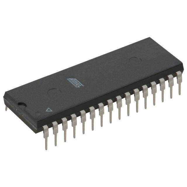
Features
• Fast Read Access Time - 120 ns
• Automatic Page Write Operation
•
•
•
•
•
•
•
•
•
– Internal Address and Data Latches for 128 Bytes
– Internal Control Timer
Fast Write Cycle Time
– Page Write Cycle Time - 10 ms Maximum
– 1 to 128-byte Page Write Operation
Low Power Dissipation
– 40 mA Active Current
– 200 µA CMOS Standby Current
Hardware and Software Data Protection
DATA Polling for End of Write Detection
High Reliability CMOS Technology
– Endurance: 104 or 105 Cycles
– Data Retention: 10 Years
Single 5V ± 10% Supply
CMOS and TTL Compatible Inputs and Outputs
JEDEC Approved Byte-wide Pinout
Commercial and Industrial Temperature Ranges
1-megabit
(128K x 8)
Paged Parallel
EEPROM
Description
The AT28C010 is a high-performance electrically-erasable and programmable readonly memory. Its 1 megabit of memory is organized as 131,072 words by 8 bits. Manufactured with Atmel’s advanced nonvolatile CMOS technology, the device offers
access times to 120 ns with power dissipation of just 220 mW. When the device is
deselected, the CMOS standby current is less than 200 µA.
(continued)
Pin Configurations
TSOP
Top View
Pin Name
Function
A0 - A16
Addresses
CE
Chip Enable
OE
Output Enable
WE
Write Enable
I/O0 - I/O7
Data Inputs/Outputs
NC
No Connect
DC
Don’t Connect
A7
A6
A5
A4
A3
A2
A1
A0
I/O0
4
3
2
1
32
31
30
VCC
WE
NC
A14
A13
A8
A9
A11
OE
A10
CE
I/O7
I/O6
I/O5
I/O4
I/O3
5
6
7
8
9
10
11
12
13
29
28
27
26
25
24
23
22
21
14
15
16
17
18
19
20
32
31
30
29
28
27
26
25
24
23
22
21
20
19
18
17
1
2
3
4
5
6
7
8
9
10
11
12
13
14
15
16
32
31
30
29
28
27
26
25
24
23
22
21
20
19
18
17
OE
A10
CE
I/O7
I/O6
I/O5
I/O4
I/O3
GND
I/O2
I/O1
I/O0
A0
A1
A2
A3
PLCC
Top View
A14
A13
A8
A9
A11
OE
A10
CE
I/O7
I/O1
I/O2
GND
I/O3
I/O4
I/O5
I/O6
1
2
3
4
5
6
7
8
9
10
11
12
13
14
15
16
A11
A9
A8
A13
A14
NC
WE
VCC
NC
A16
A15
A12
A7
A6
A5
A4
A12
A15
A16
DC
VCC
WE
NC
PDIP
Top View
NC
A16
A15
A12
A7
A6
A5
A4
A3
A2
A1
A0
I/O0
I/O1
I/O2
GND
AT28C010
Commercial /
Industrial
Note:
Rev. 0353E–06/99
PLCC package pin 1 is
DON’T CONNECT.
1
�The AT28C010 is accessed like a Static RAM for the read
or write cycle without the need for external components.
The device contains a 128-byte page register to allow writing of up to 128 bytes simultaneously. During a write cycle,
the address and 1 to 128 bytes of data are internally
latched, freeing the address and data bus for other operations. Following the initiation of a write cycle, the device will
automatically write the latched data using an internal control timer. The end of a write cycle can be detected by
DATA POLLING of I/O7. Once the end of a write cycle has
been detected a new access for a read or write can begin.
Atmel’s 28C010 has additional features to ensure high
quality and manufacturability. The device utilizes internal
error correction for extended endurance and improved data
retention characteristics. An optional software data protection mechanism is available to guard against inadvertent
writes. The device also includes an extra 128 bytes of
EEPROM for device identification or tracking.
Block Diagram
Absolute Maximum Ratings*
Temperature Under Bias................................ -55°C to +125°C
Storage Temperature ..................................... -65°C to +150°C
All Input Voltages
(including NC Pins)
with Respect to Ground ...................................-0.6V to +6.25V
All Output Voltages
with Respect to Ground .............................-0.6V to VCC + 0.6V
Voltage on OE and A9
with Respect to Ground ...................................-0.6V to +13.5V
2
AT28C010 Com/Ind
*NOTICE:
Stresses beyond those listed under “Absolute
Maximum Ratings” may cause permanent damage to the device. This is a stress rating only and
functional operation of the device at these or any
other conditions beyond those indicated in the
operational sections of this specification is not
implied. Exposure to absolute maximum rating
conditions for extended periods may affect
device reliability
�AT28C010 Com/Ind
Device Operation
READ: The AT28C010 is accessed like a Static RAM.
When CE and OE are low and WE is high, the data stored
at the memory location determined by the address pins is
asserted on the outputs. The outputs are put in the high
impedance state when either CE or OE is high. This dualline control gives designers flexibility in preventing bus contention in their system.
BYTE WRITE: A low pulse on the WE or CE input with CE
or WE low (respectively) and OE high initiates a write cycle.
The address is latched on the falling edge of CE or WE,
whichever occurs last. The data is latched by the first rising
edge of CE or WE. Once a byte write has been started it
will automatically time itself to completion. Once a programming operation has been initiated and for the duration
of tWC, a read operation will effectively be a polling operation.
PAGE WRITE: The page write operation of the AT28C010
allows 1 to 128 bytes of data to be written into the device
during a single internal programming period. A page write
operation is initiated in the same manner as a byte write;
the first byte written can then be followed by 1 to 127 additional bytes. Each successive byte must be written within
150 µs (t BLC ) of the previous byte. If the t BLC limit is
exceeded the AT28C010 will cease accepting data and
commence the internal programming operation. All bytes
during a page write operation must reside on the same
page as defined by the state of the A7 - A16 inputs. For
each WE high to low transition during the page write operation, A7 - A16 must be the same.
The A0 to A6 inputs are used to specify which bytes within
the page are to be written. The bytes may be loaded in any
order and may be altered within the same load period. Only
bytes which are specified for writing will be written; unnecessary cycling of other bytes within the page does not
occur.
DATA POLLING: The AT28C010 features DATA Polling to
indicate the end of a write cycle. During a byte or page
write cycle an attempted read of the last byte written will
result in the complement of the written data to be presented
on I/O 7. Once the write cycle has been completed, true
data is valid on all outputs, and the next write cycle may
begin. DATA Polling may begin at anytime during the write
cycle.
TOGGLE BIT: In addition to DATA Polling the AT28C010
provides another method for determining the end of a write
cycle. During the write operation, successive attempts to
read data from the device will result in I/O 6 toggling
between one and zero. Once the write has completed, I/O6
will stop toggling and valid data will be read. Reading the
toggle bit may begin at any time during the write cycle.
DATA PROTECTION: If precautions are not taken, inadvertent writes may occur during transitions of the host sys-
tem power supply. Atmel has incorporated both hardware
and software features that will protect the memory against
inadvertent writes.
HARDWARE PROTECTION: Hardware features protect
against inadvertent writes to the AT28C010 in the following
ways: (a) V CC sense—if V CC is below 3.8V (typical) the
write function is inhibited; (b) V CC power-on delay—once
VCC has reached 3.8V the device will automatically time out
5 ms (typical) before allowing a write; (c) write inhibit—
holding any one of OE low, CE high or WE high inhibits
write cycles; and (d) noise filter—pulses of less than 15 ns
(typical) on the WE or CE inputs will not initiate a write
cycle.
SOFTWARE DATA PROTECTION: A software controlled
data protection feature has been implemented on the
AT28C010. When enabled, the software data protection
(SDP), will prevent inadvertent writes. The SDP feature
may be enabled or disabled by the user; the AT28C010 is
shipped from Atmel with SDP disabled.
SDP is enabled by the host system issuing a series of three
write commands; three specific bytes of data are written to
three specific addresses (refer to Software Data Protection
Algorithm). After writing the 3-byte command sequence
and after tWC the entire AT28C010 will be protected against
inadvertent write operations. It should be noted, that once
protected the host may still perform a byte or page write to
the AT28C010. This is done by preceding the data to be
written by the same 3-byte command sequence used to
enable SDP.
Once set, SDP will remain active unless the disable command sequence is issued. Power transitions do not disable
SDP and SDP will protect the AT28C010 during power-up
and power-down conditions. All command sequences must
conform to the page write timing specifications. The data in
the enable and disable command sequences is not written
to the device and the memory addresses used in the
sequence may be written with data in either a byte or page
write operation.
After setting SDP, any attempt to write to the device without
the 3-byte command sequence will start the internal write
timers. No data will be written to the device; however, for
the duration of tWC, read operations will effectively be polling operations.
DEVICE IDENTIFICATION: An extra 128 bytes of
EEPROM memory are available to the user for device identification. By raising A9 to 12V ± 0.5V and using address
locations 1FF80H to 1FFFFH the bytes may be written to or
read from in the same manner as the regular memory
array.
OPTIONAL CHIP ERASE MODE: The entire device can
be erased using a 6-byte software code. Please see Software Chip Erase application note for details.
3
�DC and AC Operating Range
Operating
Temperature (Case)
Com.
Ind.
VCC Power Supply
AT28C010-12
AT28C010-15
AT28C010-20
0°C - 70°C
0°C - 70°C
0°C - 70°C
-40°C - 85°C
-40°C - 85°C
-40°C - 85°C
5V ± 10%
5V ± 10%
5V ± 10%
Operating Modes
Mode
CE
OE
WE
I/O
Read
VIL
VIL
VIH
DOUT
VIL
VIH
VIL
DIN
High Z
(2)
Write
Standby/Write Inhibit
(1)
VIH
X
X
Write Inhibit
X
X
VIH
Write Inhibit
X
VIL
X
Output Disable
X
VIH
X
Notes:
High Z
1. X can be VIL or VIH.
2. Refer to AC Programming Waveforms.
DC Characteristics
Symbol
Parameter
Condition
ILI
Input Load Current
ILO
Max
Units
VIN = 0V to VCC + 1V
10
µA
Output Leakage Current
VI/O = 0V to VCC
10
µA
ISB1
VCC Standby Current CMOS
CE = VCC - 0.3V to VCC + 1V
200
µA
ISB2
VCC Standby Current TTL
CE = 2.0V to VCC + 1V
3
mA
ICC
VCC Active Current
f = 5 MHz; IOUT = 0 mA
40
mA
VIL
Input Low Voltage
0.8
V
VIH
Input High Voltage
VOL
Output Low Voltage
IOL = 2.1 mA
VOH1
Output High Voltage
IOH = -400 µA
2.4
V
VOH2
Output High Voltage CMOS
IOH = -100 µA; VCC = 4.5V
4.2
V
4
Min
2.0
AT28C010 Com/Ind
V
0.45
V
�AT28C010 Com/Ind
AC Read Characteristics
AT28C010-12
Symbol
Parameter
tACC
Min
AT28C010-15
Max
Min
Max
AT28C010-20
Min
Max
Units
Address to Output Delay
120
150
200
ns
(1)
CE to Output Delay
120
150
200
ns
(2)
OE to Output Delay
0
50
0
55
0
55
ns
tDF(3)(4)
CE or OE to Output Float
0
50
0
55
0
55
ns
tOH
Output Hold from OE, CE or
Address, whichever occurred first
0
tCE
tOE
0
0
ns
AC Read Waveforms(1)(2)(3)(4)
Notes:
1. CE may be delayed up to tACC - tCE after the address transition without impact on tACC.
2. OE may be delayed up to tCE - tOE after the falling edge of CE without impact on tCE or by tACC - tOE after an address change
without impact on tACC.
3. tDF is specified from OE or CE whichever occurs first (CL = 5 pF).
4. This parameter is characterized and is not 100% tested.
Input Test Waveforms and
Measurement Level
Output Test Load
tR, tF < 5 ns
Pin Capacitance
f = 1 MHz, T = 25°C(1)
Symbol
Typ
Max
Units
Conditions
CIN
4
10
pF
VIN = 0V
COUT
8
12
pF
VOUT = 0V
Note:
1. This parameter is characterized and is not 100% tested.
5
�AC Write Characteristics
Symbol
Parameter
tAS, tOES
Address, OE Set-up Time
0
ns
tAH
Address Hold Time
50
ns
tCS
Chip Select Set-up Time
0
ns
tCH
Chip Select Hold Time
0
ns
tWP
Write Pulse Width (WE or CE)
100
ns
tDS
Data Set-up Time
50
ns
tDH, tOEH
Data, OE Hold Time
0
ns
AC Write Waveforms
WE Controlled
CE Controlled
6
AT28C010 Com/Ind
Min
Max
Units
�AT28C010 Com/Ind
Page Mode Characteristics
Symbol
Parameter
Min
Max
Units
tWC
Write Cycle Time
10
ms
tAS
Address Set-up Time
0
ns
tAH
Address Hold Time
50
ns
tDS
Data Set-up Time
50
ns
tDH
Data Hold Time
0
ns
tWP
Write Pulse Width
100
ns
tBLC
Byte Load Cycle Time
tWPH
Write Pulse Width High
150
50
µs
ns
Page Mode Write Waveforms(1)(2)
Notes:
1.
A7 through A16 must specify the same page address during each high to low transition of WE (or CE).
2.
OE must be high only when WE and CE are both low.
Chip Erase Waveforms
tS = 5 µsec (min.)
tW = tH = 10 msec (min.)
VH = 12.0V ± 0.5V
7
�Software Data Protection
Enable Algorithm(1)
Software Data Protection
Disable Algorithm(1)
LOAD DATA AA
TO
ADDRESS 5555
LOAD DATA AA
TO
ADDRESS 5555
LOAD DATA 55
TO
ADDRESS 2AAA
LOAD DATA 55
TO
ADDRESS 2AAA
LOAD DATA A0
TO
ADDRESS 5555
LOAD DATA 80
TO
ADDRESS 5555
WRITES ENABLED(2)
LOAD DATA XX
TO
ANY ADDRESS(4)
LOAD DATA AA
TO
ADDRESS 5555
LOAD LAST BYTE
TO
LAST ADDRESS
LOAD DATA 55
TO
ADDRESS 2AAA
ENTER DATA
PROTECT STATE
Notes for software program code:
1. Data Format: I/O7 - I/O0 (Hex);
Address Format: A14 - A0 (Hex).
2. Write Protect state will be activated at end of
write even if no other data is loaded.
3. Write Protect state will be deactivated at end of
write period even if no other data is loaded.
4. 1 to 128 bytes of data are loaded.
LOAD DATA 20
TO
ADDRESS 5555
EXIT DATA
PROTECT STATE(3)
LOAD DATA XX
TO
ANY ADDRESS(4)
LOAD LAST BYTE
TO
LAST ADDRESS
Software Protected Write Cycle Waveforms(1)(2)(3)
Notes:
1. A0 through A14 must conform to the addressing sequence for the first 3 bytes as shown above.
2. After the command sequence has been issued and a page write operation follows, the page address inputs (A7 - A16) must
be the same for each high to low transition of WE (or CE).
3. OE must be high only when WE and CE are both low.
8
AT28C010 Com/Ind
�AT28C010 Com/Ind
Data Polling Characteristics(1)
Symbol
Parameter
tDH
Data Hold Time
tOEH
OE Hold Time
Min
Max
OE to Output Delay
tWR
Write Recovery Time
Units
10
ns
10
ns
(2)
tOE
Notes:
Typ
ns
0
ns
1. These parameters are characterized and not 100% tested.
2. See AC Read Characteristics.
Data Polling Waveforms
Toggle Bit Characteristics(1)
Symbol
Parameter
tDH
Data Hold Time
10
ns
tOEH
OE Hold Time
10
ns
tOE
OE to Output Delay(2)
tOEHP
OE High Pulse
tWR
Write Recovery Time
Notes:
Min
Typ
Max
Units
ns
150
ns
0
ns
1. These parameters are characterized and not 100% tested.
2. See AC Read Characteristics.
Toggle Bit Waveforms
Notes:
1. Toggling either OE or CE or both OE and CE will operate toggle bit.
2. Beginning and ending state of I/O6 will vary.
3. Any address location may be used but the address should not vary.
9
�Ordering Information(1)
ICC (mA)
tACC
(ns)
Active
Standby
Ordering Code
Package
120
40
0.2
AT28C010(E)-12JC
AT28C010(E)-12PC
AT28C010(E)-12TC
32J
32P6
32T
Commercial
(0° to 70°C)
40
0.2
AT28C010(E)-12JI
AT28C010(E)-12PI
AT28C010(E)-12TI
32J
32P6
32T
Industrial
(-40° to 85°C)
40
0.2
AT28C010(E)-15JC
AT28C010(E)-15PC
AT28C010(E)-15TC
32J
32P6
32T
Commercial
(0° to 70°C)
40
0.2
AT28C010(E)-15JI
AT28C010(E)-15PI
AT28C010(E)-15TI
32J
32P6
32T
Industrial
(-40° to 85°C)
40
0.2
AT28C010(E)-20JC
AT28C010(E)-20PC
AT28C010(E)-20TC
32J
32P6
32T
Commercial
(0° to 70°C)
40
0.2
AT28C010(E)-20JI
AT28C010(E)-20PI
AT28C010(E)-20TI
32J
32P6
32T
Industrial
(-40° to 85°C)
150
200
Note:
1. See Valid Part Number table below.
Package Type
32J
32-lead, Plastic J-leaded Chip Carrier (PLCC)
32P6
32-lead, 0.600" Wide, Plastic Dual Inline Package (PDIP)
32T
32-lead, Plastic Thin Small Outline Package (TSOP)
W
Die
Options
Blank
Standard Device: Endurance = 10K Write Cycles; Write Time = 10 ms
E
High-endurance Option: Endurance = 100K Write Cycles
10
AT28C010 Com/Ind
Operation Range
�AT28C010 Com/Ind
Valid Part Numbers
The following table lists standard Atmel products that can be ordered.
Device Numbers
Speed
Package and Temperature Combinations
AT28C010
12
JC, JI, PC, PI, TC, TI
AT28C010E
12
JC, JI, PC, PI, TC, TI
AT28C010
15
JC, JI, PC, PI, TC, TI
AT28C010E
15
JC, JI, PC, PI, TC, TI
AT28C010
20
JC, JI, PC, PI, TC, TI
AT28C010E
20
JC, JI, PC, PI, TC, TI
AT28C010
-
W
Die Products
Reference Section: Parallel EEPROM Die Products
11
�Packaging Information
32J, 32-lead, Plastic J-leaded Chip Carrier (PLCC)
Dimensions in Inches and (Millimeters)
JEDEC STANDARD MS-016 AE
.045(1.14) X 45˚
PIN NO. 1
IDENTIFY
.050(1.27) TYP
.300(7.62) REF
.430(10.9)
.390(9.90)
AT CONTACT
POINTS
.030(.762)
.015(.381)
.095(2.41)
.060(1.52)
.140(3.56)
.120(3.05)
JEDEC OUTLINE MO-142 DD
INDEX
MARK
20.2(.795)
19.8(.780)
0.25(.010)
0.15(.006)
8.20(.323)
7.80(.307)
1.20(.047) MAX
0.15(.006)
0.05(.002)
0
5 REF
0.20(.008)
0.10(.004)
0.70(.028)
0.50(.020)
*Controlling dimension: millimeters
12
AT28C010 Com/Ind
.090(2.29)
MAX
1.500(38.10) REF
.220(5.59)
MAX
.005(.127)
MIN
SEATING
PLANE
.065(1.65)
.015(.381)
.022(.559)
.014(.356)
.161(4.09)
.125(3.18)
.110(2.79)
.090(2.29)
.012(.305)
.008(.203)
32T, 32-lead, Plastic Thin Small Outline Package
(TSOP)
Dimensions in Millimeters and (Inches)*
7.50(.295)
REF
.566(14.4)
.530(13.5)
.021(.533)
.013(.330)
.453(11.5)
.447(11.4)
.495(12.6)
.485(12.3)
18.5(.728)
18.3(.720)
PIN
1
.530(13.5)
.490(12.4)
.022(.559) X 45˚ MAX (3X)
0.50(.020)
BSC
1.67(42.4)
1.64(41.7)
.025(.635) X 30˚ - 45˚
.012(.305)
.008(.203)
.553(14.0)
.547(13.9)
.595(15.1)
.585(14.9)
.032(.813)
.026(.660)
32P6, 32-lead, 0.600" Wide, Plastic Dual Inline
Package (PDIP)
Dimensions in Inches and (Millimeters)
.065(1.65)
.041(1.04)
.630(16.0)
.590(15.0)
0 REF
15
.690(17.5)
.610(15.5)
�Atmel Headquarters
Atmel Operations
Corporate Headquarters
Atmel Colorado Springs
2325 Orchard Parkway
San Jose, CA 95131
TEL (408) 441-0311
FAX (408) 487-2600
Europe
1150 E. Cheyenne Mtn. Blvd.
Colorado Springs, CO 80906
TEL (719) 576-3300
FAX (719) 540-1759
Atmel Rousset
Atmel U.K., Ltd.
Coliseum Business Centre
Riverside Way
Camberley, Surrey GU15 3YL
England
TEL (44) 1276-686-677
FAX (44) 1276-686-697
Zone Industrielle
13106 Rousset Cedex
France
TEL (33) 4-4253-6000
FAX (33) 4-4253-6001
Asia
Atmel Asia, Ltd.
Room 1219
Chinachem Golden Plaza
77 Mody Road Tsimhatsui
East Kowloon
Hong Kong
TEL (852) 2721-9778
FAX (852) 2722-1369
Japan
Atmel Japan K.K.
9F, Tonetsu Shinkawa Bldg.
1-24-8 Shinkawa
Chuo-ku, Tokyo 104-0033
Japan
TEL (81) 3-3523-3551
FAX (81) 3-3523-7581
Fax-on-Demand
North America:
1-(800) 292-8635
International:
1-(408) 441-0732
e-mail
literature@atmel.com
Web Site
http://www.atmel.com
BBS
1-(408) 436-4309
© Atmel Corporation 1999.
Atmel Corporation makes no warranty for the use of its products, other than those expressly contained in the Company’s standard warranty which is detailed in Atmel’s Terms and Conditions located on the Company’s web site. The Company assumes no responsibility for
any errors which may appear in this document, reserves the right to change devices or specifications detailed herein at any time without
notice, and does not make any commitment to update the information contained herein. No licenses to patents or other intellectual property of Atmel are granted by the Company in connection with the sale of Atmel products, expressly or by implication. Atmel’s products are
not authorized for use as critical components in life support devices or systems.
Marks bearing
®
and/or
™
are registered trademarks and trademarks of Atmel Corporation.
Terms and product names in this document may be trademarks of others.
Printed on recycled paper.
0353E–06/99/xM
�