Atmel AT42QT1110-MZ
AT42QT1110-AZ
11-key QTouch® Touch Sensor IC
DATASHEET
Features
Sensor Keys:
Up to 11 QTouch® channels
Data Acquisition:
Measurement of keys triggered either by a signal applied to the SYNC pin or
at regular intervals timed by the AT42QT1110 internal clock
Keys measured sequentially for better performance, or in parallel groups for
faster operation
Raw data for key touches can be read as a report over the SPI interface
Discrete Outputs:
Configurable “Detect” outputs indicating individual key touch (7-key mode)
Device Setup:
Device configuration can be stored in EEPROM
Technology:
Patented spread-spectrum charge-transfer (direct mode)
Key Outline Sizes:
6 mm × 6 mm or larger (panel thickness dependent); widely different sizes and
shapes possible, including solid or ring shapes
Key Spacings:
7 mm center-to-center or more (panel thickness dependent)
Layers Required:
One
Electrode Materials:
Etched copper, silver, carbon, Indium Tin Oxide (ITO)
Electrode Substrates:
PCB, FPCB, plastic films, glass
Panel Materials:
Plastic, glass, composites, painted surfaces (low particle density metallic
paints possible)
Panel Thickness:
Up to 10 mm glass, 5 mm plastic (electrode size dependent)
Key Sensitivity:
Individually settable via simple commands over serial interface
Adjacent Key Suppression® (AKS®)
Patented AKS technology to enable accurate key detection
Interface:
Full-duplex SPI slave mode (1.5 MHz), CHANGE pin, discrete detection
outputs
9570J–AT42–05/2013
� Moisture Tolerance
Increased moisture tolerance based on hardware design and firmware tuning
Power:
3 V – 5.5 V
Package:
32-pin 5 × 5 mm MLF RoHS compliant
32-pin 7 × 7 mm TQFP RoHS compliant
Signal Processing:
Self-calibration, auto drift compensation, noise filtering, AKS technology
Applications:
Specific package qualified for automotive applications, such as radio, keyless entry, electric windows and satellite
navigation
AT42QT1110-MZ / AT42QT1110-AZ [DATASHEET]
9570J–AT42–05/2013
2
�SNS0K
1.2
SNS9/DETECT4
SNS8K/DETECT3
SNS9K/DETECT5
CHANGE
RESET
Pinout Configuration
SNS10K/SYNC
1.1
SNS10/DETECT6
Pinout and Schematic
SNS0
1.
1
32 31 30 29 28 27 26 25
24
SNS8/DETECT2
SNS1
2
23
SNS7/DETECT1
SNS1K
3
22
SNS7K/DETECT0
VDD
4
VSS
5
QT1110
QT1110
21
VSS
20
SNS6
SNS6K
18
VDD
SNS3
8
SCK
MOSI
MISO
SS
SNS5K
10
SNS5
9
17
11 12 13 14 15 16
SNS4
19
7
SNS4K
6
SNS2
SNS3K
SNS2K
Pin Descriptions
Table 1-1.
Pin Listing
Pin
Name
Type
Comments
If Unused, Connect To...
1
SNS0K
I/O
Sense Pin
Leave open
2
SNS1
I/O
Sense Pin
Leave open
3
SNS1K
I/O
Sense Pin
Leave open
4
Vdd
P
Power
–
5
Vss
P
Supply Ground
–
6
SNS2K
I/O
Sense Pin
Leave open
7
SNS2
I/O
Sense Pin
Leave open
8
SNS3
I/O
Sense Pin
Leave open
9
SNS3K
I/O
Sense Pin
Leave open
10
SNS4
I/O
Sense Pin
Leave open
11
SNS4K
I/O
Sense Pin
Leave open
AT42QT1110-MZ / AT42QT1110-AZ [DATASHEET]
9570J–AT42–05/2013
3
�Table 1-1.
I
O
Pin Listing (Continued)
Pin
Name
Type
Comments
If Unused, Connect To...
12
SNS5
I/O
Sense Pin
Leave open
13
SNS5K
I/O
Sense Pin
Leave open
14
SS
I
Enable SPI
15
MOSI
I
SPI Data In
Leave open
16
MISO
O
SPI Data Out
Leave open
17
SCK
I
SPI Clock
Leave open
18
Vdd
P
Power
–
19
SNS6K
I/O
Sense Pin
Leave open
20
SNS6
I/O
Sense Pin
Leave open
21
Vss
P
Supply Ground
–
22
SNS7K/DETECT0
I/O
Sense Pin/Key Status Indicator
Leave open
23
SNS7/DETECT1
I/O
Sense Pin/Key Status Indicator
Leave open
24
SNS8/DETECT2
I/O
Sense Pin / Key Status Indicator
Leave open
25
SNS8K/DETECT3
I/O
Sense Pin / Key Status Indicator
Leave open
26
SNS9/DETECT4
I/O
Sense Pin / Key Status Indicator
Leave open
27
SNS9K/DETECT5
I/O
Sense Pin / Key Status Indicator
Leave open
28
CHANGE
OD
Touch Event Indicator
Leave open
29
RESET
I
Reset
Vdd
30
SNS10/DETECT6
I/O
Sense Pin / Key Status Indicator
Leave open
31
SNS10K/SYNC
I/O
Sense Pin / Synchronization Input
Vdd or Vss via 100 k resistor
32
SNS0
I/O
Sense Pin
Leave open
Input and output
Open drain output
P
Input only
Output only, push-pull
I/O
OD
Vss via 100 k resistor to enable SPI
Vdd via 100 k resistor to disable SPI
Ground or power
AT42QT1110-MZ / AT42QT1110-AZ [DATASHEET]
9570J–AT42–05/2013
4
�Schematics
VREG
QT1110
Figure 1-1. Typical Circuit: 7 keys With Detect Outputs and No External Trigger
Vunreg
1.3
AT42QT1110-MZ / AT42QT1110-AZ [DATASHEET]
9570J–AT42–05/2013
5
�Figure 1-2. Typical Circuit: 11 Keys With No External Trigger
Vunreg
VREG
QT1110
AT42QT1110-MZ / AT42QT1110-AZ [DATASHEET]
9570J–AT42–05/2013
6
�Figure 1-3. Typical Circuit: 10 Keys With External Trigger (SYNC Mode)
Vunreg
VREG
QT1110
For component values in Figure 1-1, Figure 1-2 and Figure 1-3, check the following sections:
Section 3.1 on page 9: Cs capacitors (Cs0 – Cs10)
Section 3.2 on page 9: Sample resistors (Rs0 – Rs10)
Section 3.5 on page 10: Voltage levels
Section 3.3 on page 9: LED traces
AT42QT1110-MZ / AT42QT1110-AZ [DATASHEET]
9570J–AT42–05/2013
7
�2.
Overview of the AT42QT1110
2.1
Introduction
The AT42QT1110 (QT1110) is a digital burst mode charge-transfer (QT™) capacitive sensor driver designed for any
touch-key applications.
The keys can be constructed in different shapes and sizes. Refer to the Touch Sensors Design Guide and
Application Note QTAN0002, Secrets of a Successful QTouch Design, for more information on construction and
design methods (both downloadable from the Atmel website).
The device includes all signal processing functions necessary to provide stable sensing under a wide variety of
changing conditions, and the outputs are fully debounced. Only a few external parts are required for operation.
The QT1110 modulates its bursts in a spread-spectrum fashion in order to suppress heavily the effects of external
noise, and to suppress RF emissions.
2.2
Configurations
The QT1110 is designed as a versatile device, capable of various configurations. There are two basic configurations
for the QT1110:
11-key QTouch. The device can sense up to 11 keys.
7-key QTouch with individual outputs for each key. The device can sense up to 7 keys and drive the matching
Detect outputs to a user-configurable PWM.
Both configurations allow for a choice of acquisition modes, thus providing a variety of possibilities that will satisfy
most applications (see the following sections for more information).
Additionally, the SYNC line can be used as an external trigger input. Note that in 11-key mode the SYNC line
replaces one key, thus allowing only 10 keys.
See Section 4.7 on page 18 for more information.
2.3
Guard Channel
The device has a guard channel option (available in all key modes), which allows one key to be configured as a
guard channel to help prevent false detection. See Section 4.9 on page 20 for more information.
2.4
Self-test Functions
The QT1110 has two types of self-test functions:
Internal Hardware tests – check for hardware failures in the device internal memory.
Functional checks – confirm that the device is operating within expected parameters.
See Section 4.10 on page 20 for more information.
2.5
Moisture Tolerance
The presence of water (condensation, sweat, spilt water, and so on) on a sensor can alter the signal values
measured and thereby affect the performance of any capacitive device. The moisture tolerance of QTouch devices
can be improved by designing the hardware and fine-tuning the firmware following the recommendations in the
application note Atmel AVR3002: Moisture Tolerant QTouch Design (www.atmel.com/Images/doc42017.pdf).
AT42QT1110-MZ / AT42QT1110-AZ [DATASHEET]
9570J–AT42–05/2013
8
�3.
Wiring and Parts
3.1
Cs Sample Capacitors
Cs0 – Cs10 are the charge sensing sample capacitors. Normally they are identical in nominal value. The optimal Cs
values depend on the thickness of the panel and its dielectric constant. Thicker panels require larger values of Cs.
Values can be in the range 2.2 nF (for faster operation) to 33 nF (for best sensitivity); typical values are 4.7 nF to
10 nF.
The value of Cs should be chosen so that a light touch on a key produces a reduction of ~20 to 30 in the key signal
value (see Section 6.8 on page 27). The chosen Cs value should never be so large that the key signals exceed
~1000, as reported by the chip in the debug data.
The Cs capacitors must be X7R or PPS film type, for stability. For consistent sensitivity, they should have a 10
percent tolerance. Twenty percent tolerance may cause small differences in sensitivity from key to key and unit to
unit. If a key is not used, the Cs capacitor may be omitted.
3.2
Rs Resistors
The series resistors Rs0 – Rs10 are inline with the electrode connections and should be used to limit electrostatic
discharge (ESD) currents and to suppress radio frequency (RF) interference. Values should be approximately 2 k
to 20 k each; a typical value is 4.7 k.
Although these resistors may be omitted, the device may become susceptible to external noise or radio frequency
interference (RFI). For details of how to select these resistors see the Application Note QTAN0002, Secrets of a
Successful QTouch Design, downloadable from the Touch Technology area of the Atmel website, www.atmel.com.
3.3
LED Traces and Other Switching Signals
Digital switching signals near the sense lines can induce transients into the acquired signals, deteriorating the SNR
performance of the device. Such signals should be routed away from the sensing traces and electrodes, or the
design should be such that these lines are not switched during the course of signal acquisition (bursts).
LED terminals which are multiplexed or switched into a floating state, and which are within, or physically very near, a
key (even if on another nearby PCB) should be bypassed to either Vss or Vdd with at least a 1 nF capacitor. This is
to suppress capacitive coupling effects which can induce false signal shifts. The bypass capacitor does not need to
be next to the LED, in fact it can be quite distant. The bypass capacitor is noncritical and can be of any type.
LED terminals which are constantly connected to Vss or Vdd do not need further bypassing.
3.4
PCB Cleanliness
Modern no-clean flux is generally compatible with capacitive sensing circuits.
CAUTION: If a PCB is reworked to correct soldering faults relating to the QT1110, or to any
associated traces or components, be sure that you fully understand the nature of the flux used
during the rework process. Leakage currents from hygroscopic ionic residues can stop capacitive
sensors from functioning. If you have any doubts, a thorough cleaning after rework may be the
only safe option.
AT42QT1110-MZ / AT42QT1110-AZ [DATASHEET]
9570J–AT42–05/2013
9
�3.5
Power Supply
3.5.1
General Considerations
See Section 8.2 on page 39 for the power supply range. If the power supply fluctuates slowly with temperature, the
device tracks and compensates for these changes automatically with only minor changes in sensitivity. If the supply
voltage drifts or shifts quickly, the drift compensation mechanism is not able to keep up, causing sensitivity
anomalies or false detections.
The usual power supply considerations with QT parts apply to the device. The power should be clean and come from
a separate regulator if possible. However, this device is designed to minimize the effects of unstable power, and,
except in extreme conditions, should not require a separate Low Dropout (LDO) regulator.
See underneath Figure 1.3 on page 5 for suggested regulator manufacturers.
Caution: A regulator IC shared with other logic can result in erratic operation and is not
advised.
A single ceramic 0.1 µF bypass capacitor, with short traces, should be placed very close to the
power pins of the IC. Failure to do so can result in device oscillation, high current
consumption, or erratic operation.
It is assumed that a larger bypass capacitor (like1 µF) is somewhere else in the power circuit; for example, near the
regulator.
3.5.2
Brownout Detection
The QT1110 includes a power supply monitoring circuit that detects if Vdd drops below a safe operating voltage.
When this occurs, the device goes into a Reset state, where no acquisition or processing is carried out. The device
remains in this state until Vdd returns to the specified voltage range.
Once a safe operating voltage is detected, the QT1110 behaves as per normal power-on/reset conditions; that is,
any saved settings are restored from EEPROM, the internal self-tests are run and all channels are calibrated.
The Brown-out detector threshold is 2.7 V ±10%.
3.6
MLF Package Restrictions
The central pad on the underside of the MLF chip should be connected to ground. Do not run any tracks underneath
the body of the chip, only ground. Figure 3-1 shows examples of good and bad tracking.
Figure 3-1. Examples of Good and Bad Tracking
Example of GOOD tracking
Example of BAD tracking
AT42QT1110-MZ / AT42QT1110-AZ [DATASHEET]
9570J–AT42–05/2013
10
�4.
Detailed Operations
4.1
Communications
4.1.1
Introduction
All communication with the device is carried out over the Serial Peripheral Interface (SPI). This is a synchronous
serial data link that operates in full-duplex mode. The host communicates with the QT controller over the SPI using a
master-slave relationship, with the QT1110 acting in slave mode.
4.1.2
SPI Operation
The SPI uses four logic signals:
Serial Clock (SCK) – output from the host.
Master Output, Slave Input (MOSI) – output from the host, input to the QT controller. Used by the host to send
data to the QT controller.
Master Input, Slave Output (MISO) – input to the host, output from the QT controller. Used by the QT device to
send data to the host.
Slave Select (SS) – active low output from the host.
At each byte, the master pulls SS low and generates 8 clock pulses on SCK. With these 8 clock pulses, a byte of
data is transmitted from the master to the slave over MOSI, most significant bit (msb) first.
Simultaneously a byte of data is transmitted from the slave to the master over MISO, also most significant bit first.
The slave reads the status of MOSI at the leading edge of each clock pulse, and the master reads the slave data
from MISO at the trailing edge.
The QT1110 requires that the clock idles “high”, meaning that the data on MOSI and MISO pins are set at the falling
edges and sampled at the rising edges.
That is:
Clock polarity CPOL = 1
Clock phase CPHA = 1
The QT1110 SPI interface can operate at any SCK frequency up to 1.5 MHz.
In multibyte communications, the master must pause for a minimum delay of 150 µs between the completion of one
byte exchange and the beginning of the next.
Note that the number of bytes to be transmitted depends on the initial command sent by the host. This sets the mode
on the QT1110 so that the QT1110 knows how to respond to, or how to interpret, the following bytes. If there is a
delay of >100 ms between bytes while the QT1110 is waiting for data, or waiting to send data, then the incomplete
transmission is discarded and the device resets its SPI state machine. It will then interpret the next byte it receives as
a fresh command.
When the QT1110 SPI interface is receiving a new command, it returns the Idle status code (0x55) on MISO during
the first byte exchange to indicate to the master that it is in the correct state for receiving instructions.
4.1.3
CRC Bytes
If enabled, a CRC checking procedure is implemented on all communications between the SPI master and the
QT1110. In this case, each command or report request sent by the master must have a byte appended containing
the CRC checksum of the data sent. The QT1110 will not respond to commands until the CRC byte has been
received and verified.
Sample C code showing the algorithm for calculating the CRC of the data can be found in Appendix A..
AT42QT1110-MZ / AT42QT1110-AZ [DATASHEET]
9570J–AT42–05/2013
11
�When the QT1110 is expecting a CRC byte, it returns (on MISO) the calculated CRC byte which it expects to
receive. This is sent simultaneously with the QT1110 receiving the CRC byte from the master (that is, during the
same byte exchange). This allows both devices to confirm that the data was sent correctly.
All data returned by the QT1110 is also be followed by a CRC byte, allowing the master to confirm the integrity of the
data transmission.
4.1.4
SPI Commands
There are three types of communication between the SPI master and the QT1110:
Control commands (see Section 5. on page 22)
To send control instructions to the QT1110
Report requests (see Section 6. on page 25)
Setup commands (see Section 7. on page 29)
To reading status information from the QT1110
To set configuration options (“Set” instructions)
To read configuration options (“Get” instructions)
Additionally the NULL command (0x00) is transmitted by the host device as it is receiving data from the QT1110.
4.1.4.1 Control Commands
A control command is an instruction sent to the QT1110 that controls operations of the device, and for which no
response is required. Examples of control commands are: Reset, Calibrate, Send Setups.
With the exception of Send Setups, control commands normally require a single byte exchange, unless CRC
checking is enabled, in which case a second byte must be transmitted by the host with the calculated CRC of the
command byte.
Figure 4-1. Sleep Command – CRC Disabled
Host (Sends on MOSI)
Device (Responds on MISO)
Command: 0x05
Response: 0x55 (“Idle” – Fresh Command)
Simultaneous
Transmission
Figure 4-2. Sleep Command – CRC Enabled
Host (Sends on MOSI)
Device (Responds on MISO)
Command: 0x05
Response: 0x55 (“Idle” – Fresh Command)
Simultaneous
Transmission
Command CRC: 0x3F
Response: 0x3F (Expected Command CRC)
AT42QT1110-MZ / AT42QT1110-AZ [DATASHEET]
9570J–AT42–05/2013
12
�When the Send Setups command is received, the QT1110 stops measurement of QTouch sensors and waits for 42
bytes of data to be sent. Only when all 42 bytes have been received (and the CRC byte, if CRC is enabled), the
QT1110 applies all the settings to RAM and resumes measurement. In this case, if CRC is enabled, the CRC byte is
calculated for all the data sent by the host, including the command byte 0x01.
Control Commands are specified in detail in Section 5. on page 22.
4.1.5
Report Requests
Report Requests are sent by the Host to instruct the QT1110 to return status information. The host sends the
appropriate Report Request command, then transmits Null bytes on MOSI while the QT1110 returns the report data
on MISO.
Figure 4-3. All Keys Report – CRC Disabled
Host (Sends on MOSI)
Device (Responds on MISO)
Command: 0xC1
Response: 0x55 (“Idle” – Fresh Command)
Simultaneous
Transmission
Null: 0x00
Key Status Report Byte 0
Null: 0x00
Key Status Report Byte 1
For example, Figure 4-3 shows the exchange that takes place to read the 2-byte All Keys report. In this exchange,
the host sends:
0xC1 — 0x00 — 0x00
and the QT1110 returns (simultaneously):
0x55 — Report Byte 0 — Report Byte 1
If CRC is enabled, this exchange is extended to 5 bytes, as shown in Figure 4-4 on page 14.
AT42QT1110-MZ / AT42QT1110-AZ [DATASHEET]
9570J–AT42–05/2013
13
�Figure 4-4. All Keys Report – CRC Enabled
Host (Sends on MOSI)
Device (Responds on MISO)
Command: 0xC1
Response: 0x55 (“Idle” – Fresh Command)
Simultaneous
Transmission
Command CRC: 0x94
Response: 0x94 (Expected Command CRC)
Null: 0x00
Key Status Report Byte 0
Null: 0x00
Key Status Report Byte 1
Null: 0x00
Report CRC: 0x??
4.1.5.1 Set Instructions
Set Instructions are 2-byte transmissions by the host that are used to send settings to individual locations in the
device memory map.
At the first byte, the QT1110 returns 0x55 (Idle) to confirm that it will interpret the byte as a new command. At the
second byte, the QT1110 returns the Set command it has just received.
For example, to set the Positive Recalibration Delay to 1920 ms, address 5 in the memory map is set to 12 (0x0C).
This is done with the Set command for address 5 (command code 0x95), as shown in Figure 4-5.
Figure 4-5. Positive Recalibration Delay Set Instruction – CRC Disabled
Host (Sends on MOSI)
Device (Responds on MISO)
Command: 0x95
Response: 0x55 (“Idle” – Fresh Command)
Simultaneous
Transmission
“Set” Data: 0x0C
Response: 0x95 (Command Just Received)
AT42QT1110-MZ / AT42QT1110-AZ [DATASHEET]
9570J–AT42–05/2013
14
�With CRC Enabled, a CRC byte is also required (Figure 4-6). This is calculated for the two transmitted bytes (that is,
the Set command and the data byte).
For example, for the sequence shown in Figure 4-5 (0x95 — 0x0C), the CRC Byte is 0x9F. As is the case with the
other command types, when the QT1110 is expecting a CRC byte from the host, it calculates that byte in advance
and returns the expected value to the host in the same transmission as the host sends the CRC byte.
The sent data is not applied to the memory location until the CRC byte has been received and verified.
Figure 4-6. Positive Recalibration Delay Set Instruction – CRC Enabled
Host (Sends on MOSI)
Device (Responds on MISO)
Command: 0x95
Response: 0x55 (“Idle” – Fresh Command)
Simultaneous
Transmission
“Set” Data: 0x0C
Response: 0x95 (Command Just Received)
Command CRC: 0x9F
Response: 0x9F (Expected CRC)
4.1.5.2 Get Instructions
Get instructions are instructions that read the data from a location in the QT1110 memory map.
Figure 4-7. Positive Recalibration Delay Get Instruction – CRC Disabled
Host (Sends on MOSI)
Device (Responds on MISO)
Command: 0xD5
Response: 0x55 (“Idle” – Fresh Command)
Simultaneous
Transmission
Null: 0x00
“Get” Data: 0x0C (Positive Recalibration Delay)
The host sends the appropriate Get command, followed by a Null byte. The QT1110 returns the contents of the
addressed memory location.
Figure 4-7 shows the exchange for a report on the positive recalibration delay (assuming that the data byte is 0x0C).
With CRC Enabled, this exchange takes 4 bytes, with a command CRC transmitted by the host and a report CRC
returned by the QT1110 (see Figure 4-8 on page 16).
AT42QT1110-MZ / AT42QT1110-AZ [DATASHEET]
9570J–AT42–05/2013
15
�Figure 4-8. Positive Recalibration Delay Get Instruction – CRC Enabled
Host (Sends on MOSI)
Device (Responds on MISO)
Command: 0xD5
Simultaneous
Transmission
Response: 0x55 (“Idle” – Fresh Command)
Command CRC: 0x68
Response: 0x68 (Expected Command CRC)
Null: 0x00
“Get” Data: 0x0C (Positive Recalibration Delay)
Null: 0x00
“Get” CRC: 0xA3
4.1.6
Quick SPI Mode
4.1.6.1 Introduction
In Quick SPI Mode, the QT1110 sends a 7-byte key report at each exchange. No host commands are required over
SPI in this mode; the host clocks the data bytes out in sequence. Quick SPI mode is enabled by setting the SPI_EN
bit in the Comms Options setup byte (see Section 7.5 on page 31).
4.1.6.2 Quick SPI Report
The 7 report bytes are in the format given in Table 4-1.
Table 4-1.
Byte
Device Status Report Format
Description
Bit 7
Bit 6
Bit 5
Bit 4
Bit 3
Bit 2
Bit 1
Bit 0
0
Counter
Counter – increments from 0 to 255
1
Detect status, channels 0 – 3
Channel 3
Channel 2
Channel 1
Channel 0
2
Detect status, channels 4 – 7
Channel 7
Channel 6
Channel 5
Channel 4
3
Detect status, channels 8 – 10
Reserved
Channel 10
Channel 9
Channel 8
4
Error status, channels 0 – 3
Channel 3
Channel 2
Channel 1
Channel 0
5
Error status, channels 4 – 7
Channel 7
Channel 6
Channel 5
Channel 4
6
Error status, channels 8 – 10
Reserved
Channel 10
Channel 9
Channel 8
AT42QT1110-MZ / AT42QT1110-AZ [DATASHEET]
9570J–AT42–05/2013
16
�where:
Byte 0 is a counter that increments from 0 to 254 on successive exchanges to confirm that firmware is
operating correctly.
Bytes 1 – 3 indicate the detect status of channels 0 – 3, 4 – 7 and 8 – 10 respectively (two bits per channel),
as follows:
00 = Channel not in detect
01 = Channel in detect
10 = Not Allowed
11 = Invalid Signal (Channel disabled)
Bytes 4 – 6 indicate the error status of channels 0 – 3, 4 – 7 and 8 – 10 respectively (two bits per channel), as
follows:
00 = No error
01 = Not allowed
10 = Error on channel
11 = Invalid signal (channel disabled)
Successive byte exchanges in Quick SPI mode cycle through the 7 bytes of status information. If synchronization is
lost, the host must either re-synchronize by identifying the incrementing counter byte (byte 0) or pausing
communications for at least 100 ms so the QT1110 will reset its SPI state.
4.1.6.3 Commands in Quick SPI Mode
Only two host commands are recognized under Quick SPI mode. These are shown in Table 4-2.
Table 4-2.
Host Commands in Quick SPI Mode
Command
Code
Purpose
Store to EEPROM
0x0A
Allows for “Quick SPI mode” to be stored as the default start-up mode
Enable Full SPI
0x36
Enables full SPI mode
CRC checking is not implemented in Quick SPI mode for host commands or return data.
4.1.6.4 Quick SPI Mode timing
In Quick SPI mode, the minimum time between byte exchanges is reduced to 50 µS.
If a pause in communications of 100 ms is detected during reading of the 7-byte report, the QT1110 resets the
exchange, and on the next byte read it returns byte 0 of the report.
4.2
Reset
The QT1110 can be reset using one of two methods:
Hardware reset: An external reset logic line can be used if desired, fed into the RESET pin. However, under
most conditions it is acceptable to tie RESET to Vdd.
Software reset: A software reset can be forced using the “Reset” control command.
For both methods, the device will follow the same initialization sequence. If there any saved settings in the
EEPROM, these are loaded into RAM. Otherwise the default settings are applied.
Note:
The SPI interface becomes active after the QT1110 has completed its startup sequence, taking
approximately 160 ms after power on/reset.
AT42QT1110-MZ / AT42QT1110-AZ [DATASHEET]
9570J–AT42–05/2013
17
�4.3
Sleep Mode
The QT1110 can be put into a very low power sleep mode (typically < 2 µA). During sleep mode, no keys are
measured and the DETECT outputs are all put into high impedance mode to minimize current consumption. The
device remains in sleep mode until a falling edge is detected on either the SS pin or the CHANGE pin. When the
QT1110 wakes from sleep mode, it continues to operate as it was before it was put into sleep mode. The QT1110
requires approximately 100 µs to wake from sleep mode and will not respond correctly to SPI communications until
the wake-up procedure is complete. The low level on the SS or CHANGE pin that is used to wake the device must be
maintained for 100 µs to ensure correct operation.
Note:
4.4
If the device is set to sleep mode for an extended period, the host should initiate a recalibration immediately
after waking the QT1110.
Calibration
The device can be forced to recalibrate the sensor keys at any time. This can be useful where, for example, a
portable device is plugged into mains power, or during product development when settings are being tuned.
The QT1110 can also be configured to automatically recalibrate if it remains in detection for too long. This avoids
keys becoming “stuck” after a prolonged period of uninterrupted detection. See Section 7.18 on page 38 for details.
4.5
CHANGE Pin
The CHANGE pin can be configured using the Comms Options setup byte (see Section 7.5 on page 31) to act in one
of two modes:
4.6
Data mode
The CHANGE pin is asserted (pulled low) when the detection status of a key changes from that last
sent to the host; that is when a key-touch or key-release event occurs.
The CHANGE pin is pulled low when a key status changes and is only released when the “Send All
keys” report is requested (0xC1), or the key status information bytes are read in Quick SPI mode (see
Section 7.5 on page 31).
Touch mode
The CHANGE pin is pulled low when one or more keys are in detect. The CHANGE pin remains low as
long as there is a key in detect, regardless of communications.
The CHANGE pin is released when there are no keys in detect. No host communications are required to
release the CHANGE pin.
Stand-alone Mode
The QT1110 can operate in a stand-alone mode without the use of the SPI interface. The settings are loaded from
EEPROM and the device operates in 7-key mode using the Detect outputs.
4.7
Key Modes
4.7.1
11-key Mode
In 11-key mode, the device can sense up to 11 keys. Alternatively, one key can be replaced by the SYNC line as an
external trigger input (see Section 4.8.2 on page 19).
11-key mode is configured by setting the MODE bit in the Device Mode setup byte (see Section 7.4 on page 30).
Key acquisition can be triggered in one of two ways: using the internal clock to trigger acquisition either at a fixed
repetition period or in a continuous “free run” mode (see Section 4.8.1), or using the SYNC pin to provide an external
trigger (see Section 4.8.2 on page 19),
AT42QT1110-MZ / AT42QT1110-AZ [DATASHEET]
9570J–AT42–05/2013
18
�4.7.2
7-key Mode
In 7-key mode, the detect outputs DETECT0 to DETECT6 become active on pins 22 – 27 and 30. These outputs
provide configurable PWM signals that indicate when each of the keys is touched.
7-key mode is configured by clearing the MODE bit in the Device Mode setup byte (see Section 7.4 on page 30).
Each DETECT output can be individually configured to output a PWM signal while the matching key is in detect or
out of detect. This signal can be one of nine levels, ranging from low (PWM = 0%) to high (PWM = 100%). This
allows for the use of an indicating LED. This is achieved by enabling the appropriate bit in the Key to LED setup byte
(see Section 7.14 on page 36), and setting the desired outputs levels or PWMs in setup addresses 9 to 15 (see
Section 7.12 on page 34).
4.8
Trigger Modes
4.8.1
Timed Trigger
In 11-key mode, The QT1110 can be configured to use the internal clock as a timed trigger. In this case, the QT1110
is configured with a cycle period, such that each acquisition cycle starts a specified length of time after the start of
the previous cycle. If the cycle period is set to 0, each acquisition cycle starts as soon as the previous one has
finished, resulting in the acquisition cycles running back-to-back in a “free run” mode.
The use of a timed trigger, and the cycle period to be used, is set in the Device Mode setup byte (see Section 7.4 on
page 30).
4.8.2
Synchronized Trigger
In 11-key mode, if a time trigger is not enabled, the QT1110 operates in “synchronized” mode. In this mode, SNS10K
is used as a SYNC pin to trigger key acquisition, rather than using the device internal clock. In this case the
maximum number of keys is reduced to 10.
The SYNC pin can use one of two methods to trigger key measurements, selectable via bit 4 of the Device Mode
setup byte (see Section 7.4 on page 30): Low Level and Rising Edge.
With the Low Level method the QT1110 operates in “free run” mode for as long as the SYNC pin is read as a logical
0. When the SYNC pin goes high, the current measurement cycle will be finished and no more key measurements
will be taken until the SYNC pin goes low again. The low level trigger should be a minimum of 1 ms so that there is
sufficient time for the device to detect the low level.
With the Rising Edge method all enabled keys are measured once when a rising edge is detected on the SYNC pin.
This allows key measurements to be synchronized to an external event or condition.
For example, the SYNC pin can be used by the host to synchronize several devices to each other. This would ensure
that only one of the devices outputs pulses at any given time and signals from one QT1110 do not interfere with the
measurements from another.
Another use for synchronizing to the rising edge is to steady the signals when the device is running off a mains
transformer with insufficient mains frequency filtering that is causing a 50 Hz or 60 Hz ripple on Vdd. If the mains
voltage is scaled down with a simple voltage divider and connected to the SYNC pin, then the key measurement can
be triggered by the rising edge detected at a positive going zero-crossing. Note that in this case, each key signal will
be taken at the same point in the cycle, so Vdd will be the same at each measurement for a given key and the
signals will be steadier.
AT42QT1110-MZ / AT42QT1110-AZ [DATASHEET]
9570J–AT42–05/2013
19
�4.9
Guard Channel Option
The device has a guard channel option (available in all key modes), which allows one key to be configured as a
guard channel to help prevent false detection (see Figure 4-9 on page 20). Guard channel keys should be more
sensitive than the other keys (physically bigger or larger Cs), subject to burst length limitations (see Section 4.11.2
on page 21).
With guard channel enabled, the designated key is connected to a sensor pad which detects the presence of touch
and overrides any output from the other keys using the chip AKS feature. The guard channel option is enabled by the
Guard Key setup byte (see Section 7.5 on page 31).
With the guard channel not enabled, all the keys work normally.
Note:
If a key is already “in detect” when the guard channel becomes active, that key will remain in detect and the
guard key will not activate until the active key goes out of detect.
Figure 4-9. Guard Channel Example
Key Pad Formed
of Six Keys
Guard Channel
Formed of One Key
4.10
Self-test Functions
4.10.1 Internal Hardware Tests
Internal hardware tests check for hardware failure in the device internal memory areas and data paths. Any failure
detected in the function or contents of application ROM, RAM or registers causes the device to reset itself.
The application code is scanned with a CRC check routine to confirm that the application data is all correct.
The RAM and registers are checked periodically (every 10 seconds) for dynamic and static failures.
4.10.2 Functional Checks
Functional checks confirm that the device is operating within expected parameters; any failure detected in these
tests is notified to the system host. The device will continue to operate in the event that such functional failures are
detected.
The functional tests are:
Check that the channel-measurement signals are within the defined range.
Confirm that data stored in the EEPROM is valid.
These tests are carried out as the particular functions are used. For example, the EEPROM is checked when the
device attempts to load data from EEPROM, and the channel signals are checked when a measurement is carried
out.
Note:
If a particular channel is unused, the threshold of that channel should be set to 0 to prevent the incorrect
reporting of the unused channel as being in an error state.
AT42QT1110-MZ / AT42QT1110-AZ [DATASHEET]
9570J–AT42–05/2013
20
�4.11
Signal Processing
4.11.1 Detection Integrator
The device features a detection integration mechanism, which acts to confirm a detection in a robust fashion. A perkey counter is incremented each time the key has exceeded its threshold. When this counter reaches a preset limit
the key is finally declared to be touched. For example, if the DI limit is set to 10, then a key signal must fall by more
than the key threshold, and remain below that level for 10 acquisitions, before the key is declared to be touched.
Similarly, the DI is applied to a key that is going out of detect: it must take 10 acquisitions where the signal has not
exceeded its detect threshold before it is declared to leave touch.
4.11.2 Burst Length Limitations
The maximum burst length is 2048 pulses. The recommended design is to use a capacitor that gives a signal of
)�
)"7)
����
8�
8�
)"9)
����
�
8�
8�
��A �
B
)"�)
8
#$%&
8
�������
�
��
�����
���������
���
�
��
����
������
� �!"��
�����
������*�����
�*�7F7F�")�
�?��G*�@�
������E
)"7)
*��"�)
��&F�������
�*�
��G�%E��*
+��������E�H.
��+!
��#��@�
���
��
���,
H+#/
���
������� �
�
��
�
�
������
�
AT42QT1110-MZ / AT42QT1110-AZ [DATASHEET]
9570J–AT42–05/2013
44
�8.9.2
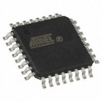
AT42QT1110-AZ – 32-pin 7 x 7 mm TQFP
��
�
�
&
&�
<
?$%%$��
1&C
%$��
1&C
�
)AJ:A
��
@
��
�$��$#��1�&#'1$#'
,2�����3���
�.���4�
/
�
'1�&�
1&C
#������ �����"���%E����
��
������3�� �����(&�&����3��������'�)�9*�
��
������?�"�
� �����������������"����� �����������
���&������������!.��� �!�������.����"���!!��


 工商网监
湘ICP备2023018690号
工商网监
湘ICP备2023018690号
