Features
• Complies with Intel® Low-Pin Count (LPC) Interface Specification Revision 1.1
– Supports both Firmware Hub (FWH) and LPC Memory Read and Write Cycles
• Auto-detection of FWH and LPC Memory Cycles
•
•
•
•
•
•
•
– Can Be Used as FWH for Intel 8xx, E7xxx, and E8xxx Series Chipsets
– Can Be Used as LPC Flash for Non-Intel Chipsets
Top Boot with Bottom Partitioned Memory Array for Efficient Vital Data Storage
– 64-Kbyte Top Boot Sector, Six 64-Kbyte Sectors, One 32-Kbyte Sector, One
16-Kbyte Sector, Two 8-Kbyte Sectors
– Or Memory Array Can Be Divided Into Eight Uniform 64-Kbyte Sectors for Erasing
Two Configurable Interfaces
– FWH/LPC Interface for In-System Operation
– Address/Address Multiplexed (A/A Mux) Interface for Programming during
Manufacturing
FWH/LPC Interface
– Operates with the 33 MHz PCI Bus Clock
– 5-signal Communication Interface Supporting Byte Reads and Writes
– Two Hardware Write Protect Pins: TBL for Top Boot Sector and WP for All
Other Sectors
– Five General-purpose Input (GPI) Pins for System Design Flexibility
– Identification (ID) Pins for Multiple Device Selection
– Sector Locking Registers for Individual Sector Read and Write Protection
A/A Mux Interface
– 11-pin Multiplexed Address and 8-pin Data Interface
– Facilitates Fast In-System or Out-of-System Programming
Single Voltage Operation
– 3.0V to 3.6V Supply Voltage for Read and Write Operations
Industry-Standard Package Options
– 32-lead PLCC
– 40-lead TSOP
Green (Pb/Halide-free) Packaging Option
4-megabit
Top Boot,
Bottom
Partitioned
Firmware Hub
and Low-Pin
Count Flash
Memory
AT49LH00B4
Not Recommended
for New Design
Contact Atmel to discuss
the latest design in trends
and options
1. Description
The AT49LH00B4 is a Flash memory device designed for use in PC and notebook
BIOS applications. The device complies with version 1.1 of Intel’s LPC Interface Specification, providing support for both FWH and LPC memory read and write cycles. The
device can also automatically detect the memory cycle type to allow the AT49LH00B4
to be used as a FWH with Intel chipsets or as an LPC Flash with non-Intel chipsets.
The sectoring of the AT49LH00B4’s memory array has been optimized to meet the
needs of today’s BIOS applications. By optimizing the size of the sectors, the BIOS
code memory space can be used more efficiently. Because certain BIOS code modules must reside in their own sectors by themselves, the wasted and unused memory
space that occurred with previous generation BIOS Flash memory devices can be
greatly reduced. This increased memory space efficiency allows additional BIOS routines to be developed and added while still maintaining the same overall device
density.
3379C–FLASH–3/05
�The memory array of the AT49LH00B4 can be sectored in two ways simply by using two different erase commands. Using one erase command allows the device to contain a total of eleven
sectors comprised of a 64-Kbyte boot sector, six 64-Kbyte sectors, a 32-Kbyte sector, a
16-Kbyte sector, and two 8-Kbyte sectors. The 64-Kbyte boot sector is located at the top (uppermost) of the device’s memory address space and can be hardware write protected by using the
TBL pin. Alternatively, by using a different erase command, the memory array can be arranged
into eight even erase sectors of 64-Kbyte each.
The AT49LH00B4 supports two hardware interfaces: The FWH/LPC interface for In-System
operations and the A/A Mux interface for programming during manufacturing. The Interface Configuration (IC) pin of the device provides the control between these two interfaces. An internal
Command User Interface (CUI) serves as the control center between the device interfaces and
the internal operation of the nonvolatile memory. A valid command sequence written to the CUI
initiates device automation.
Specifically designed for use in 3-volt systems, the AT49LH00B4 supports read, program, and
erase operations with a supply voltage range of 3.0V to 3.6V. No separate voltage is required for
programming and erasing.
The AT49LH00B4 utilizes fixed program and erase times, independent of the number of program and erase cycles that have occurred. Therefore, the system does not need to be calibrated
or correlated to the cumulative number of program and erase cycles.
2
AT49LH00B4
3379C–FLASH–3/05
�AT49LH00B4
2. Pin Configurations
32PLCC
29
28
27
26
25
24
23
22
21
14
15
16
17
18
19
20
5
6
7
8
9
10
11
12
13
IC [IC]
GND
NC
NC
VCC
INIT [OE]
FWH4/LFRAME [WE]
RES [RDY/BSY]
RES [I/O7]
[I/O1] FWH1/LAD1
[I/O2] FWH2/LAD2
GND
[I/O3] FWH3/LAD3
[I/O4] RES
[I/O5] RES
[I/O6] RES
[A7] GPI1
[A6] GPI0
[A5] WP
[A4] TBL
[A3] ID3
[A2] ID2
[A1] ID1
[A0] ID0
[I/O0] FWH0/LAD0
4
3
2
1
32
31
30
GPI2 [A8]
GPI3 [A9]
RST [RST]
NC
VCC
CLK [R/C]
GPI4 [A10]
2.1
2.2
40TSOP
NC
[IC] IC
NC
NC
NC
NC
[A10] GPI4
NC
[R/C] CLK
VCC
NC
[RST] RST
NC
NC
[A9] GPI3
[A8] GPI2
[A7] GPI1
[A6] GPI0
[A5] WP
[A4] TBL
Note:
1
2
3
4
5
6
7
8
9
10
11
12
13
14
15
16
17
18
19
20
40
39
38
37
36
35
34
33
32
31
30
29
28
27
26
25
24
23
22
21
GND
VCC
FWH4/LFRAME [WE]
INIT [OE]
RES [RDY/BSY]
RES [I/O7]
RES [I/O6]
RES [I/O5]
RES [I/O4]
VCC
GND
GND
FWH3/LAD3 [I/O3]
FWH2/LAD2 [I/O2]
FWH1/LAD1 [I/O1]
FWH0/LAD0 [I/O0]
ID0 [A0]
ID1 [A1]
ID2 [A2]
ID3 [A3]
[ ] Designates A/A Mux Interface.
3
3379C–FLASH–3/05
�3. Block Diagram
TBL
CLK
FWH4/LFRAME
FWH/LAD[3:0]
WP
INIT
FWH/LPC
INTERFACE
CONTROL LOGIC
I/O BUFFERS
AND LATCHES
INTERFACE CONTROL
AND LOGIC
IC
RST
R/C
A[10:0]
I/O[7:0]
OE
WE
A/A MUX
INTERFACE
ADDRESS LATCH
ID[3:0]
GPI[4:0]
Y-DECODER
Y-GATING
X-DECODER
FLASH
MEMORY
ARRAY
RDY/BSY
4. Device Memory Map
4
Sector
Type
Size (Bytes)
Address Range
10
Main Sector
64K
070000H - 07FFFFH
9
Main Sector
64K
060000H - 06FFFFH
8
Main Sector
64K
050000H - 05FFFFH
7
Main Sector
64K
040000H - 04FFFFH
6
Main Sector
64K
030000H - 03FFFFH
5
Main Sector
64K
020000H - 02FFFFH
4
Main Sector
64K
010000H - 01FFFFH
3
Sub-sector
32K
008000H - 00FFFFH
2
Sub-sector
16K
004000H - 007FFFH
1
Sub-sector
8K
002000H - 003FFFH
0
Sub-sector
8K
000000H - 001FFFH
AT49LH00B4
3379C–FLASH–3/05
�AT49LH00B4
5. Pin Description
Table 5-1 provides a description of each of the device pins. Most of the pins have dual functionality in that they are used for
both the FWH/LPC interface as well as the A/A Mux interface.
Table 5-1.
Signal Descriptions
Interface
Symbol
Name and Function
FWH/LPC
A/A Mux
Type
IC
INTERFACE COMMUNICATION: The IC pin determines which interface is
operational. If the IC pin is held high, then the A/A Mux interface is enabled, and if
the IC pin is held low, then the FWH/LPC interface is enabled. The IC pin must be
set at power-up or before returning from a reset condition and cannot be changed
during device operation.
The IC pin is internally pulled-down with a resistor valued between 20 kΩ and
100 kΩ, so connection of this pin is not necessary if the FWH/LPC interface will
always be used in the system. If the IC pin is driven high to enable the A/A Mux
interface, then the pin will exhibit some leakage current.
X
X
Input
CLK
FWH/LPC CLOCK: This pin is used to provide a clock to the device. This pin is
usually connected to the 33 MHz PCI clock and adheres to the PCI specification.
This pin is used as the R/C pin in the A/A Mux interface.
X
Input
FWH4/
LFRAME
FWH INPUT/LPC FRAME: This pin is used to indicate the start of a FWH or LPC
data transfer operation. The pin is also used to abort a FWH or LPC cycle in
progress.
This pin is used as the WE pin in the A/A Mux interface.
X
Input
FWH/
LAD[3:0]
FWH/LPC ADDRESS AND DATA: These pins are used for FWH/LPC bus
information such as addresses, data, and command inputs/outputs.
These pins are used as the I/O[3:0] pins in the A/A Mux interface.
X
Input/
Output
RST
INTERFACE RESET: The RST pin is used for both FWH/LPC and A/A Mux
interfaces. When the RST pin is driven low, write operations are inhibited, internal
automation is reset, and the FWH/LAD[3:0] pins (when using the FWH/LPC
interface) are put into a high-impedance state. When the device exits the reset
state, it will default to the read array mode.
X
INIT
PROCESSOR RESET/INITIALIZE: The INIT pin is used as a second reset pin for
In-System operation and functions identically to the RST pin. The INIT pin is
designed to be connected to the chipset’s INIT signal.
The maximum voltage to be applied to the INIT pin depends on the processor’s or
chipset’s specifications. Systems must take care to not violate processor or chipset
specifications regarding the INIT pin voltage.
This pin is used as the OE pin in the A/A Mux interface.
X
Input
TBL
TOP BOOT SECTOR LOCK: When the TBL pin is held low, program and erase
operations cannot be performed to the 64-Kbyte top boot sector regardless of the
state of the Sector Locking Registers. Please refer to the Sector Protection section
for more details.
If the TBL pin is held high, then hardware write protection for the top boot sector will
be disabled. However, register-based sector protection will still apply. The state of
the TBL pin does not affect the state of the Sector Locking Registers.
This pin is used as the A4 pin in the A/A Mux interface.
X
Input
X
Input
5
3379C–FLASH–3/05
�Table 5-1.
Signal Descriptions (Continued)
Interface
Symbol
Name and Function
WP
WRITE PROTECT: When the WP pin is low, program and erase operations to all
sectors except for the 64-Kbyte top boot sector cannot be performed regardless of
the state of the Sector Locking Registers. See “Sector Protection” on page 19. for
more details.
If the WP pin is high, then hardware write protection for all of the sectors except the
top boot sector will be disabled. Register-based sector protection, however, will still
apply. The state of the WP pin does not affect the state of the Sector Locking
Registers.
This pin is used as the A5 pin in the A/A Mux interface.
X
Input
ID[3:0]
IDENTIFICATION INPUTS: These four pins are part of the mechanism that allows
multiple devices to be attached to the same bus. The strapping of these pins is
used to assign an ID to each device. The boot device must have ID[3:0] = 0000,
and it is recommended that all subsequent devices should use sequential up-count
strapping (e.g., 0001, 0010, 0011, etc.).
The ID[3:0] pins are internally pulled-down with resistors valued between 20 kΩ
and 100 kΩ when using the FWH/LPC interface, so connection of these pins is not
necessary if only a single device will be used in a system. Any pins intended to be
low may be left floating. Any ID pin driven high will exhibit some leakage current.
These pins are used as the A[3:0] pins in the A/A Mux interface.
X
Input
GPI[4:0]
GENERAL-PURPOSE INPUTS: The individual GPI pins can be used for additional
board flexibility. The state of the GPI pins can be read, using the FWH/LPC
interface, through the GPI register. The GPI pins should be at their desired state
before the start of the PCI clock cycle during which the read is attempted, and they
should remain at the same level until the end of the read cycle.
The voltages applied to the GPI pins must comply with the devices VIH and VIL
requirements. Any unused GPI pins must not be left floating.
These pins are used as the A[10:6] pins in the A/A Mux interface.
X
Input
A[10:0]
ADDRESS INPUTS: These pins are used for inputting the multiplexed address
values when using the A/A Mux interface. The addresses are latched by the rising
and falling edge of R/C pin.
X
Input
I/O[7:0]
DATA INPUTS/OUTPUTS: The I/O pins are used in the A/A Mux interface to input
data and commands during write cycles and to output data during memory array,
Status Register, and identifier code read cycles. Data is internally latched during a
write cycle.
The I/O pins will be in a high-impedance state when the outputs are disabled.
X
Input/
Output
R/C
ROW/COLUMN ADDRESS SELECT: In the A/A Mux interface, the R/C pin is used
to latch the address values presented on the A[10:0] pins. The row addresses
(A10 - 0) are latched on the falling edge of R/C, and the column addresses
(A18 - A11) are latched on the rising edge of R/C.
X
Input
OE
OUTPUT ENABLE: The OE pin is used in the A/A Mux interface to control the
device’s output buffers during a read cycle.
The I/O[7:0] pins will be in high-impedance state when the OE pin is deasserted
(high).
X
Input
WE
WRITE ENABLE: The WE pin is used in the A/A Mux interface to control write
operations to the device.
X
Input
6
FWH/LPC
A/A Mux
Type
AT49LH00B4
3379C–FLASH–3/05
�AT49LH00B4
Table 5-1.
Signal Descriptions (Continued)
Interface
Symbol
Name and Function
RDY/BSY
READY/BUSY: The RDY/BSY pin provides the device’s ready/busy status when
using the A/A Mux interface. The RDY/BSY pin is a reflection of Status Register
bit 7, which is used to indicate whether a program or erase operation has been
completed.
Use of the RDY/BSY pin is optional, and the pin does not need to be connected.
VCC
DEVICE POWER SUPPLY: The VCC pin is used to supply the source voltage to
the device. Program and erase operations are inhibited when VCC is less than or
equal to VLKO.
Operations at invalid VCC voltages may produce spurious results and should not be
attempted.
GND
FWH/LPC
A/A Mux
Type
X
Output
X
X
Power
GROUND: The ground reference for the power supply. GND should be connected
to the system ground.
X
X
Power
NC
NO CONNECT: NC pins have no internal connections and can be driven or left
floating. If the pins are driven, the voltage levels should comply with VIH and VIL
requirements.
X
X
–
RES
RESERVED: RES pins are reserved for future device enhancements or
functionality. These pins may be left floating or may be driven. If the pins are driven,
the voltage levels should comply with VIH and VIL requirements.
These pins are used as the RDY/BSY and I/O[7:4] pins in the A/A Mux interface.
X
X
–
6. Interface Selection
The AT49LH00B4 can operate in two distinct interface modes: The FWH/LPC interface and the
A/A Mux interface. Selection of the interface is determined by the state of the IC pin. When the
IC pin is held low, the device will operate using the FWH/LPC interface. Alternatively, when the
IC pin is held high, the device will operate using the A/A Mux interface.
7. FWH/LPC Interface
The FWH/LPC interface is designed as an In-System interface used in communicating with
either the I/O Controller Hub (ICH) in Intel chipsets or typically the PCI south bridge in non-Intel
chipsets.
The FWH/LPC interface uses a 5-signal communication interface consisting of a 4-bit data bus,
the FWH/LAD[3:0] pins, and one control line, the FWH4/LFRAME pin. The operation and timing
of the interface is based on the 33 MHz PCI clock, and the buffers for the FWH/LPC interface
are PCI compliant. To ensure the effective delivery of security and manageability features, the
FWH/LPC interface is the only way to get access to the full feature set of the device.
Commands, addresses, and data are transferred via the FWH/LPC interface using a series of
fields. The field sequences and contents are strictly defined for FWH and LPC memory cycles.
These field sequences are detailed in the FWH Interface Operation and LPC Interface Operation
sections.
Since the AT49LH00B4 can be used as either a FWH Flash or an LPC Flash, the device is capable of automatically detecting which type of memory cycle is being performed. For a FWH/LPC
cycle, the host will drive the FWH4/LFRAME pin low for one or more clock cycles to initiate the
operation. After driving the FWH4/LFRAME pin low, the host will send a START value to indicate
7
3379C–FLASH–3/05
�the type of FWH/LPC cycle that is to be performed. The value of the START field determines
whether the device will operate using a FWH cycle or an LPC cycle. Table 7-1 details the three
valid START fields that the device will recognize.
Table 7-1.
FWH/LPC Start Fields
START Value
Cycle Type
0000b
LPC Cycle – The type (memory, I/O, DMA) and direction of the cycle (read or write)
is determined by the second field (CYCTYPE + DIR) of the LPC cycle. Only memory
cycles are supported by the device.
1101b
FWH Memory Read Cycle
1110b
FWH Memory Write Cycle
If a valid START value is not detected, then the device will enter standby mode when the
FWH4/LFRAME pin is high and no internal operation is in progress. The FWH/LAD[3:0] pins will
also be placed in a high-impedance state.
7.1
FWH4/LFRAME Pin
FWH4/LFRAME is used by the master to indicate the start of cycles and the termination of
cycles due to an abort or time-out condition. This signal is to be used by peripherals to know
when to monitor the bus for a cycle.
The FWH4/LFRAME signal is used as a general notification that the FWH/LAD[3:0] lines contain
information relative to the start or stop of a cycle, and that peripherals must monitor the bus to
determine whether the cycle is intended for them. The benefit to peripherals of FWH4/LFRAME
is that it allows them to enter lower power states internally when a cycle is not intended for them.
When peripherals sample FWH4/LFRAME is active, they are to immediately stop driving the
FWH/LAD[3:0] signal lines on the next clock and monitor the bus for new cycle information.
7.2
FWH/LAD[3:0] Pins
The FWH/LAD[3:0] signal lines communicate address, control, and data information over the
LPC bus between a master and a peripheral. The information communicated are: start, stop
(abort a cycle), transfer type (memory, I/O, DMA), transfer direction (read/write), address, data,
wait states, DMA channel, and bus master grant.
7.3
FWH Memory Cycles
A valid FWH memory cycle begins with the host driving the FWH4/LFRAME signal low for one or
more clock cycles. While the FWH4/LFRAME signal is low, a valid START value of either 1101b
(FWH memory read) or 1110b (FWH memory write) must be driven on the FWH/LAD[3:0] pins.
Following the START field, an IDSEL (Device Select) field must be sent to the device. The
IDSEL field acts like a chip select in that it indicates which device should respond to the current
operation. After the IDSEL field has been sent, the 7-clock MADDR (Memory Address) field
must be sent to the device to provide the 28-bit starting address location of where to begin reading or writing in the memory. Following the MADDR field, the MSIZE (Memory Size) field must
be sent to indicate the number of bytes to transfer.
8
AT49LH00B4
3379C–FLASH–3/05
�AT49LH00B4
Figure 7-1.
FWH Memory Cycle Initiation and Addressing
CLK
FWH4/LFRAME
FWH/LAD[3:0]
7.3.1
START
IDSEL
MADDR MADDR MADDR MADDR MADDR MADDR MADDR
MSIZE
Start Field
This 1-clock field indicates the start of a cycle. It is valid on the last clock that FWH4/LFRAME is
sampled low. The two start fields that are used for a FWH cycle are: 1101b to indicate a FWH
memory read cycle and 1110b to indicate a FWH memory write cycle. If the start field that is
sampled is not one of these values, then the cycle attempted is not a FWH memory cycle. It may
be a valid LPC memory cycle that the device will attempt to decode.
7.3.2
IDSEL (Device Select) Field
This 1-clock field is used to indicate which FWH component in the system is being selected. The
four bits transmitted over FWH/LAD[3:0] during this clock are compared with values strapped on
the ID[3:0] pins. If there is a match, the device will continue to decode the cycle to determine
which bytes are requested on a read or which bytes to update on a write. If there isn’t a match,
the device may discard the rest of the cycle and go into a standby power state.
7.3.3
MADDR (Memory Address) Field
This is a 7-clock field that is used to provide a 28-bit (A27 - A0) memory address. This allows for
provisioning of up to 256 MB per FWH memory device, for a total of a 4 GB addressable space if
16 FWH memory devices (256 MB each) were used in a system.
The AT49LH00B4 only decodes the last six MADDR nibbles (A23 - A0) and ignores address bits
A27 - A23 and A21 - A19. Address bit A22 is used to determine whether reads or writes to the
device will be directed to the memory array (A22 = 1) or to the register space (A22 = 0).
Addresses are transferred to the device with the most significant nibble first.
7.3.4
Msize (Memory Size) Field
The 1-clock MSIZE is used to indicate how many bytes of data will be transferred during a read
or write. The AT49LH00B4 only supports single-byte transfers, so 0000b must be sent in this
field to indicate a single-byte transfer.
7.3.5
Additional Fields for FWH Memory Cycles
Additional fields are required to complete a FWH read or write cycle. The placement of these
fields, in addition to the data field, depends on whether the cycle is a FWH read or write. The
FWH Read Cycle and FWH Write Cycle sections detail the order of the various fields.
7.3.6
TAR (Turn-around) Field
This 2-clock field is driven by the master when it is turning control over to the FWH memory
device, and it is driven by the FWH device when it is turning control back over to the master. On
the first clock of the TAR field, the master or FWH drives the FWH/LAD[3:0] lines to 1111b. On
the second clock, the master or FWH device puts the FWH/LAD[3:0] lines into a high-impedance
state.
9
3379C–FLASH–3/05
�7.3.7
SYNC (Synchronize) Field
This field is used to add wait-states for an access. It can be several clocks in length. On target
cycles, this field is driven by the FWH memory device. If the FWH device needs to assert waitstates, it does so by driving a “wait” SYNC value of 0101b on the FWH/LAD[3:0] pins until it is
ready. When ready, the device will drive a “ready” SYNC value of 0000b on the FWH/LAD[3:0]
lines. Valid values for the SYNC field are shown in Table 7-2.
Table 7-2.
7.4
Valid SYNC Values
SYNC Value
SYNC Type
0000b
RSYNC (Ready SYNC) – Synchronization has been achieved with no error.
0101b
WSYNC (Wait SYNC) – Device is indicating wait-states (also referred to as
short-sync).
FWH Read Cycle
FWH read cycles are used to read data from the memory array, the Sector Locking Registers,
the GPI register, the Status Register, and to read the product ID information. Upon initial device
power-up or after exiting from a reset condition, the device will automatically default to the read
array mode.
Valid FWH read cycles begin with a START field of 1101b being sent to the device. Following
the IDSEL, MADDR, and MSIZE fields, a 2-clock TAR field must be sent to the device to indicate
that the master is turning control of the LPC bus over to the FWH memory device. After the second clock of the TAR phase, the FWH device assumes control of the bus and begins driving
SYNC fields to add wait-states. When the device is ready to output data, it will first send a
“ready” SYNC and then output one byte of data during the next two clock cycles. The data is
sent one nibble at a time with the low nibble being output first followed by the high nibble. After
the data has been output, the FWH device will send a 2-clock TAR field to the master to indicate
that it is turning control of the LPC bus back over to the master.
Table 7-2 shows a FWH read cycle that requires three SYNC clocks to access data from the
memory array.
Figure 7-2.
FWH Read Cycle
1
2
3
4
5
6
7
8
9
10
11
12
13
A27-A24 A23-A20 A19-A16 A15-A12 A11-A8
A7-A4
A3-A0
0000b
1111b
High-Z
0101b
MSIZE
TAR0
TAR1
WSYNC
14
15
16
17
18
19
0101b
0000b
D3-D0
D7-D4
1111b
High-Z
WSYNC
RSYNC
DATA
DATA
TAR0
TAR1
CLK
FWH4/LFRAME
FWH/LAD[3:0]
10
1101b
IDSEL
START
IDSEL
MADDR
AT49LH00B4
3379C–FLASH–3/05
�AT49LH00B4
Table 7-3.
Clock Cycle
FWH Read Cycle
Field Name
Field Value(1)
FWH/LAD[3:0]
FWH/LAD[3:0]
Direction
Comments
1
START
1101b
IN
FWH4/LFRAME must be active (low) for the device to
respond. Only the last START field (before FWH4/LFRAME
transitioning high) should be recognized. The START field
contents indicate a FWH memory read cycle.
2
IDSEL
0000b to 1111b
IN
Indicates which FWH memory device should respond. If the
IDSEL field matches the strapping values on ID[3:0], then that
particular device will respond to subsequent commands.
3-9
MADDR
YYYY
IN
These seven clock cycles make up the 28-bit memory
address. YYYY is one nibble of the entire address. Addresses
are transferred with the most significant nibble first.
10
MSIZE
0000b
(indicates
1 byte)
IN
The MSIZE field indicates how many bytes will be transferred.
The device only supports single-byte operations, so MSIZE
must be 0000b.
11
TAR0
1111b
IN then float
In this clock cycle, the master has driven the bus to all 1s and
then floats the bus prior to the next clock cycle. This is the first
part of the bus “turn-around cycle”.
12
TAR1
1111b (float)
Float then OUT
The device takes control of the bus during this clock cycle.
13 - 14
WSYNC
0101b (wait)
OUT
The device outputs the value 0101b, a “wait” SYNC, for two
clock cycles. This value indicates to the master that data is not
yet available from the device. This number of wait-syncs is a
function of the device’s memory access time.
15
RSYNC
0000b (ready)
OUT
During this clock cycle, the device will generate a “ready”
SYNC indicating that the least significant nibble of the data
byte will be available during the next clock cycle.
16
DATA
YYYY
OUT
YYYY is the least significant nibble of the data byte.
17
DATA
YYYY
OUT
YYYY is the most significant nibble of the data byte.
18
TAR0
1111b
OUT then float
19
TAR1
1111b (float)
Float then IN
The FWH memory device drives the bus to 1111b to indicate a
turn-around cycle.
The FWH memory device floats its outputs, and the master
regains control of the bus during this clock cycle.
Note:
1. Field contents are valid on the rising edge of the present clock cycle.
7.5
FWH Write Cycle
FWH write cycles are used to send commands to the device and to program data into the memory array.
Valid FWH write cycles begin with a START field of 1110b being sent to the device. Following
the IDSEL, MADDR, and MSIZE fields, the master sends one byte of data to the FWH device
during the next two clock cycles. The data is sent one nibble at a time with the low nibble being
output first followed by the high nibble. After the data has been sent, the master will send a
2-clock TAR field to the FWH device to indicate that it is turning control of the LPC bus back over
to the FWH. After the second clock of the TAR phase, the FWH device assumes control of the
bus and drives a “ready” SYNC field to verify that it has received the data. The FWH device will
then send a 2-clock TAR field to the master to indicate that it is turning control of the bus back
over to the master.
11
3379C–FLASH–3/05
�Figure 7-3.
FWH Write Cycle
1
2
3
4
5
6
7
8
9
10
11
12
13
14
15
16
17
A27-A24 A23-A20 A19-A16 A15-A12 A11-A8
A7-A4
A3-A0
0000b
D3-D0
D7-D4
1111b
MSIZE
DATA
DATA
TAR0
High-Z
0000b
1111b
High-Z
TAR1
RSYNC
TAR0
TAR1
CLK
FWH4/LFRAME
FWH/LAD[3:0]
Table 7-4.
Clock Cycle
Note:
12
1110b
IDSEL
START
IDSEL
MADDR
FWH Write Cycle
Field Name
Field Value(1)
FWH/LAD[3:0]
FWH/LAD[3:0
] Direction
Comments
1
START
1110b
IN
FWH4/LFRAME must be active (low) for the device to respond.
Only the last START field (before FWH4/LFRAME transitioning
high) should be recognized. The START field contents indicate a
FWH memory write cycle.
2
IDSEL
0000b to 1111b
IN
Indicates which FWH memory device should respond. If the
IDSEL field matches the strapping values on ID[3:0], then that
particular device will respond to subsequent commands.
3-9
MADDR
YYYY
IN
These seven clock cycles make up the 28-bit memory address.
YYYY is one nibble of the entire address. Addresses are
transferred with the most significant nibble first.
10
MSIZE
0000b
(indicates
1 byte)
IN
The MSIZE field indicates how many bytes will be transferred.
The device only supports single-byte operations, so MSIZE
must be 0000b.
11
DATA
YYYY
IN
YYYY is the least significant nibble of the data byte. The data
byte is either any valid Flash command or the data to be
programmed into the memory array.
12
DATA
YYYY
IN
YYYY is the most significant nibble of the data byte.
13
TAR0
1111b
IN then float
14
TAR1
1111b (float)
Float then
OUT
15
RSYNC
0000b (ready)
OUT
During this clock cycle, the device will generate a “ready” SYNC
indicating that the data byte has been received.
16
TAR0
1111b
OUT then float
The FWH memory device drives the bus to 1111b to indicate a
turn-around cycle.
17
TAR1
1111b (float)
Float then IN
In this clock cycle, the master has driven the bus to all 1s and
then floats the bus prior to the next clock cycle. This is the first
part of the bus “turn-around cycle”.
The device takes control of the bus during this clock cycle.
The FWH memory device floats its outputs, and the master
regains control of the bus during this clock cycle.
1. Field contents are valid on the rising edge of the present clock cycle.
AT49LH00B4
3379C–FLASH–3/05
�AT49LH00B4
7.6
LPC Memory Cycles
A valid LPC memory cycle begins with the host driving the FWH4/LFRAME signal low for one or
more clock cycles. While the FWH4/LFRAME signal is low, a valid START value of 0000b must
be driven on the FWH/LAD[3:0] pins. Following the START field, a CYCTYPE + DIR (Cycle Type
and Direction) field must be sent to the device to indicate the type of cycle (e.g., memory access,
I/O access, etc.) and the direction (read or write) of the transfer. After the CYCTYPE + DIR field
has been sent, the 8-clock MADDR (Memory Address) field must be sent to the device to provide the 32-bit starting address location of where to begin reading or writing in the memory.
Figure 7-4.
LPC Memory Cycle Initiation and Addressing
CLK
FWH4/LFRAME
FWH/LAD[3:0]
7.6.1
START
CYCTYPE
+ DIR
MADDR MADDR MADDR MADDR MADDR MADDR MADDR MADDR
Start Field
This 1-clock field indicates the start of a cycle. It is valid on the last clock that FWH4/LFRAME is
sampled low. The start field that is used for an LPC cycle is 0000b. If the start field that is sampled is not 0000b, then the cycle attempted is not an LPC memory cycle. It may be a valid FWH
memory cycle that the device will attempt to decode.
7.6.2
CYCTYPE + DIR (Cycle Type And Direction) Field
This 1-clock field is used to indicate the type of cycle and the direction of the transfer to be performed. Of the four bits placed on the FWH/LAD[3:0] pins, bits[3:2] must be 01b to indicate that
the transfer will be a memory cycle. Values other than 01b, which may be used to specify an I/O
cycle or a DMA cycle for other components in the system, will cause the device to enter standby
mode when the FWH4/LFRAME pin is brought high and no internal operation is in progress. The
FWH/LAD[3:0] pins will also be placed in a high-impedance state.
Bit[1] is used to determine the direction of the transfer. 0 is used to indicate a read, and 1 is used
to indicate a write. Bit[0] is ignored and reserved for future use. Table 7-5 details the two valid
CYCTYPE + DIR fields that the device will respond to.
Table 7-5.
7.6.3
Valid CYCTYPE + DIR Values
FWH/LAD[3:0]
Cycle Type
010xb
LPC Memory Read
011xb
LPC Memory Write
MADDR (Memory Address) Field
This is an 8-clock field that is used to provide a 32-bit (A31 - A0) memory address. The 32
address bits allow for the provisioning to access up to 4 GB of memory space.
The AT49LH00B4 only decodes the last six MADDR nibbles (A23 - A0) and ignores address bits
A31 - A24. Address bit A23 is used to determine whether reads or writes to the device will be
directed to the memory array (A23 = 1) or to the register space (A23 = 0).
Unlike FWH memory cycles, LPC cycles do not use an IDSEL field to determine which LPC
device in the system is being selected. Instead, the strapping values on the ID[3:0] pins are
compared against address bits A22 - A19 in the MADDR field. For the actual comparison, the
13
3379C–FLASH–3/05
�strapped values are internally inverted. For example, if ID3 was strapped to GND, a logical value
of 1 would be compared against address bit A22. If the inverted states of the ID[3:0] pins match
with address bits A22 - A19, then the device will continue to decode the rest of cycle (see LPC
Multiple Device Selection for mode details).
Addresses are transferred to the device with the most significant nibble first.
7.6.4
Additional Fields for LPC Memory Cycles
Additional fields are required to complete an LPC read or write cycle. The placement of these
fields, in addition to the data field, depends on whether the cycle is an LPC read or write. The
LPC Read Cycle and LPC Write Cycle sections detail the order of the various fields.
7.6.5
TAR (Turn-around) Field
This 2-clock field is driven by the master when it is turning control over to the LPC memory
device, and it is driven by the LPC device when it is turning control back over to the master. On
the first clock of the TAR field, the master or LPC device drives the FWH/LAD[3:0] lines to
1111b. On the second clock, the master or LPC device puts the FWH/LAD[3:0] lines into a highimpedance state.
7.6.6
SYNC (Synchronize) Field
This field is used to add wait-states for an access. It can be several clocks in length. On target
cycles, this field is driven by the LPC memory device. If the LPC device needs to assert waitstates, it does so by driving a “wait” SYNC value of 0101b on the FWH/LAD[3:0] pins until it is
ready. When ready, the device will drive a “ready” SYNC value of 0000b on the FWH/LAD[3:0]
lines. Valid values for the SYNC field are shown in Table 7-6.
Table 7-6.
14
Valid SYNC Values
SYNC Value
SYNC Type
0000b
RSYNC (Ready SYNC) – Synchronization has been achieved with no error.
0101b
WSYNC (Wait SYNC) – Device is indicating wait-states (also referred to as
short-sync).
AT49LH00B4
3379C–FLASH–3/05
�AT49LH00B4
7.7
LPC Read Cycle
LPC read cycles are used to read data from the memory array, the Sector Locking Registers, the
GPI register, the Status Register, and the product ID information. Upon initial device power-up or
after exiting from a reset condition, the device will automatically default to the read array mode.
Valid LPC read cycles begin with a START field of 0000b and a CYCTYPE + DIR field of 010xb
being sent to the device. Following the MADDR field, a 2-clock TAR field must be sent to the
device to indicate that the master is turning control of the LPC bus over to the LPC memory
device. After the second clock of the TAR phase, the LPC device assumes control of the bus
and begins driving SYNC fields to add wait-states. When the device is ready to output data, it
will first send a “ready” SYNC and then output one byte of data during the next two clock cycles.
The data is sent one nibble at a time with the low nibble being output first followed by the high
nibble. After the data has been output, the LPC device will send a 2-clock TAR field to the master to indicate that it is turning control of the LPC bus back over to the master.
Figure 7-4 shows a LPC read cycle that requires three SYNC clocks to access data from the
memory array.
Figure 7-5.
LPC Read Cycle
1
2
3
4
5
6
7
8
9
A31-A28 A27-A24 A23-A20 A19-A16 A15-A12 A11-A8
A7-A4
10
11
12
13
1111b
High-Z
0101b
TAR0
TAR1
WSYNC
14
15
16
17
18
19
0101b
0000b
D3-D0
D7-D4
1111b
High-Z
WSYNC
RSYNC
DATA
DATA
TAR0
TAR1
CLK
FWH4/LFRAME
FWH/LAD[3:0]
0000b
010xb
START
CYCTYPE
+ DIR
MADDR
A3-A0
15
3379C–FLASH–3/05
�Table 7-7.
Clock Cycle
LPC Read Cycle
Field Name
Field Value(1)
FWH/LAD[3:0]
FWH/LAD[3:0]
Direction
Comments
1
START
0000b
IN
FWH4/LFRAME must be active (low) for the device to
respond. Only the last START field (before FWH4/LFRAME
transitioning high) should be recognized. The START field
contents indicate an LPC cycle.
2
CYCTYPE +
DIR
010xb
IN
Indicates that the cycle type is an LPC memory cycle and the
direction of the transfer is a read.
3 - 10
MADDR
YYYY
IN
These eight clock cycles make up the 32-bit memory address.
YYYY is one nibble of the entire address. Addresses are
transferred with the most significant nibble first.
11
TAR0
1111b
IN then float
In this clock cycle, the master has driven the bus to all 1s and
then floats the bus prior to the next clock cycle. This is the first
part of the bus “turn-around cycle”.
12
TAR1
1111b (float)
Float then OUT
The device takes control of the bus during this clock cycle.
13 - 14
WSYNC
0101b (wait)
OUT
The device outputs the value 0101b, a “wait” SYNC, for two
clock cycles. This value indicates to the master that data is not
yet available from the device. This number of wait-syncs is a
function of the device’s memory access time.
15
RSYNC
0000b (ready)
OUT
During this clock cycle, the device will generate a “ready”
SYNC indicating that the least significant nibble of the data
byte will be available during the next clock cycle.
16
DATA
YYYY
OUT
YYYY is the least significant nibble of the data byte.
17
DATA
YYYY
OUT
YYYY is the most significant nibble of the data byte.
18
TAR0
1111b
OUT then float
19
TAR1
1111b (float)
Float then IN
The LPC memory device drives the bus to 1111b to indicate a
turn-around cycle.
The LPC memory device floats its outputs, and the master
regains control of the bus during this clock cycle.
Note:
1. Field contents are valid on the rising edge of the present clock cycle.
7.8
LPC Write Cycle
LPC write cycles are used to send commands to the device and to program data into the memory array.
Valid LPC write cycles begin with a START field of 0000b and a CYCTYPE + DIR field of 011xb
being sent to the device. Following the MADDR field, the master sends one byte of data to the
LPC device during the next two clock cycles. The data is sent one nibble at a time with the low
nibble being output first followed by the high nibble. After the data has been sent, the master will
send a 2-clock TAR field to the LPC device to indicate that it is turning control of the bus back
over to the LPC device. After the second clock of the TAR phase, the LPC device assumes control of the bus and drives a “ready” SYNC field to verify that it has received the data. The LPC
device will then send a 2-clock TAR field to the master to indicate that it is turning control of the
bus back over to the master.
16
AT49LH00B4
3379C–FLASH–3/05
�AT49LH00B4
Figure 7-6.
LPC Write Cycle
1
2
3
4
5
6
7
8
9
A31-A28 A27-A24 A23-A20 A19-A16 A15-A12 A11-A8
A7-A4
10
11
12
13
14
15
16
17
D3-D0
D7-D4
1111b
DATA
DATA
TAR0
High-Z
0000b
1111b
High-Z
TAR1
RSYNC
TAR0
TAR1
CLK
FWH4/LFRAME
FWH/LAD[3:0]
Table 7-8.
Clock Cycle
Note:
0000b
011xb
START
CYCTYPE
+ DIR
A3-A0
MADDR
LPC Write Cycle
Field Name
Field Value(1)
FWH/LAD[3:0]
FWH/LAD[3:0]
Direction
Comments
1
START
0000b
IN
FWH4/LFRAME must be active (low) for the device to
respond. Only the last START field (before FWH4/LFRAME
transitioning high) should be recognized. The START field
contents indicate an LPC cycle.
2
CYCTYPE +
DIR
011xb
IN
Indicates that the cycle type is an LPC memory cycle and the
direction of the transfer is a write.
3 - 10
MADDR
YYYY
IN
These eight clock cycles make up the 32-bit memory address.
YYYY is one nibble of the entire address. Addresses are
transferred with the most significant nibble first.
11
DATA
YYYY
IN
YYYY is the least significant nibble of the data byte. The data
byte is either any valid Flash command or the data to be
programmed into the memory array.
12
DATA
YYYY
IN
YYYY is the most significant nibble of the data byte.
13
TAR0
1111b
IN then float
14
TAR1
1111b (float)
Float then OUT
The device takes control of the bus during this clock cycle.
15
RSYNC
0000b (ready)
OUT
During this clock cycle, the device will generate a “ready”
SYNC indicating that the data byte has been received.
16
TAR0
1111b
OUT then float
17
TAR1
1111b (float)
Float then IN
In this clock cycle, the master has driven the bus to all 1s and
then floats the bus prior to the next clock cycle. This is the first
part of the bus “turn-around cycle”.
The LPC memory device drives the bus to 1111b to indicate a
turn-around cycle.
The LPC memory device floats its outputs, and the master
regains control of the bus during this clock cycle.
1. Field contents are valid on the rising edge of the present clock cycle.
17
3379C–FLASH–3/05
�8. Response to Invalid FWH/LPC Fields
During FWH/LPC operations, the device will not explicitly indicate that it has received invalid
field sequences. The response to specific invalid fields or sequences is as follows:
8.1
8.1.1
FWH Cycles
ID mismatch
If the IDSEL field does not match ID[3:0], then the device will ignore the FWH cycle. The device
will then enter standby mode when the FWH4/LFRAME pin is brought high and no internal operation is in progress. The FWH/LAD[3:0] pins will also be placed in a high-impedance state.
8.1.2
Address out of range
The FWH address sequences is seven fields long (28 bits), but only the last six address fields
(A23 - A0) will be decoded. Therefore, address bits A27 - A24 will be ignored. In addition,
because of the device density, address bits A23 and A21 - A19 will be ignored. Address bit A22
is used to determine whether reads or writes to the device will be directed to the memory array
(A22 = 1) or to the register space (A22 = 0).
8.1.3
Invalid MSIZE field
If the device receives an invalid size field during a read or write operation, the internal state
machine will reset and no operation will be attempted. The device will generate no response of
any kind in this situation. Invalid size fields for a read or write cycle are anything but 0000b. In
addition, when accessing register space, invalid field sizes are anything but 0000b.
Once valid START, IDSEL, and MSIZE fields are received, the device will always respond to
subsequent inputs as if they were valid. As long as the states of FWH/LAD[3:0] and
FWH4/LFRAME are known, the response of the device to signals received during the FWH
cycle should be predictable. The device will make no attempt to check the validity of incoming
Flash operation commands.
8.2
8.2.1
LPC Cycles
Address out of range
The LPC address sequences is eight fields long (32 bits), but only the last six address fields
(A23 - A0) will be decoded. Therefore, address bits A31 - A24 will be ignored. Address bits A22
- A19 will be decoded based on the strapping values on the ID[3:0] pins. Address bit A23 is used
to determine whether reads or writes to the device will be directed to the memory array (A23 = 1)
or to the register space (A23 = 0).
Once valid START and CYCTYPE + DIR fields are received, the device will always respond to
subsequent inputs as if they were valid. As long as the states of FWH/LAD[3:0] and
FWH4/LFRAME are known, the response of the device to signals received during the LPC cycle
should be predictable. The device will make no attempt to check the validity of incoming Flash
operation commands.
9. Bus Abort
The Bus Abort operation can be used to immediately abort the current bus operation. A Bus
Abort occurs when FWH4/LFRAME is driven low for one or more clock cycles after the start of a
bus cycle. The memory will place the FWH/LAD[3:0] pins in a high-impedance state, and the
18
AT49LH00B4
3379C–FLASH–3/05
�AT49LH00B4
internal state machine will reset. During a write cycle, there is the possibility that an internal
Flash write or erase operation may be in progress (or has just been initiated). If the
FWH4/LFRAME pin is asserted during this time frame, the internal operation will not abort. However, the internal state machine will not initiate a Flash write or erase operation until it has
received the last nibble from the host. This means that FWH4/LFRAME can be asserted as late
as clock cycle 12 (see Table 7-4 and Table 7-8) and no internal Flash operation will be
attempted.
When the FWH4/LFRAME pin has been driven low to abort a cycle, the host may issue a
START field of 1111b (stop/abort) to return the interface to the ready mode.
10. Device Reset
Asserting RST or INIT initiates a device reset. In read mode, RST or INIT low deselects the
memory, places the output drivers in a high-impedance state, and turns off all internal circuits.
RST or INIT must be held low for the minimum specified tPLPH time (FWH/LPC and A/A Mux
operations). The device resets to read array mode upon return from reset, and all Sector Locking Registers are reset to their default (write-locked) state. Since all Sector Locking Registers
are reset, all sectors in the memory array are set to the write-locked status regardless of their
locked state prior to reset.
A reset recovery time (tPHFV using the FWH/LPC interface and tPHAV using the A/A Mux interface)
is required from RST or INIT switching back high until writes to the CUI are recognized. A reset
latency will occur if a reset procedure is performed during a programming or erase operation.
During sector erase or program, driving RST or INIT low will abort the operation underway in
addition to causing a reset latency. Memory contents being altered are no longer valid since the
data may be partially erased or programmed.
It is important to assert RST or INIT during system reset. When the system comes out of reset, it
will expect to read from the memory array of the device. If a system reset occurs with no
FWH/LPC device reset (this will be hardware dependent), it is possible that proper CPU initialization will not occur (the FWH/LPC memory may be providing status information instead of
memory array data).
11. Sector Protection
Sectors in the memory array can be protected from program and erase operations using a hardware controlled method and/or a software (register-based) controlled method.
11.1
Hardware Write Protection
Two pins are available to provide hardware write protection capabilities. The Top Boot Sector
Lock (TBL) pin, when held low, prevents program and sector erase operations to the top sector
of the device (sector 10) where critical code can be stored.
When the TBL pin is high, hardware write protection for program and erase operations to the top
sector is disabled. Provided that the Write-Lock bits in the Sector Locking Registers are not set
(detailed later), sector erase or program commands can then be issued to the device to erase
the top 64-Kbyte sector (sector 10).
The Write Protect (WP) pin, which operates independently from the TBL pin, serves the same
basic function as the TBL pin for the remaining sectors except the top boot sector. When the WP
pin is held low, program and sector erase operations to sectors 9 through 0 will not be allowed.
19
3379C–FLASH–3/05
�Table 11-1.
Hardware Write Protection Options
Sector
Size (Bytes)
Address Range
Hardware Write Protection
10
64K
070000H - 07FFFFH
TBL
9
64K
060000H - 06FFFFH
WP
8
64K
050000H - 05FFFFH
WP
7
64K
040000H - 04FFFFH
WP
6
64K
030000H - 03FFFFH
WP
5
64K
020000H - 02FFFFH
WP
4
64K
010000H - 01FFFFH
WP
3
32K
008000H - 00FFFFH
WP
2
16K
004000H - 007FFFH
WP
1
8K
002000H - 003FFFH
WP
0
8K
000000H - 001FFFH
WP
The TBL and WP pins must be set to the desired protection state prior to starting a program or
erase operation because they are sampled at the beginning of the operation. Changing the state
of TBL or WP during a program or erase operation may cause unpredictable results. The new
lock status will take place after the program or erase operation completes.
The TBL and WP pins function independently from the Sector Locking Registers. These pins,
when active, will write protect the appropriate sector(s) against program and erase operations
regardless of the values of the Sector Locking Registers. For example, when TBL is active, writing to the top sector is prevented regardless of the state of the Write-Lock bit for the top sector’s
locking register. In such a case, clearing the Write-Lock bit in the Sector Locking Register will
have no functional effect even though the register may indicate that the sector is no longer
locked. However, the register may still be set to Read-Lock the sector if desired.
For protecting the sectors of the memory array, the TBL and WP pins always take precedence
over the Sector Locking Registers. In addition, the states of the TBL and WP pins have no effect
on the values or status of the Sector Locking Registers.
11.2
Register-Based Sector Locking
The device has eleven Sector Locking Registers that are used in lieu of or in conjunction with
the TBL and WP pins to control the lock protection for each sector in the memory array. The
Sector Locking Registers are accessed through their respective address locations (detailed in
Table 11-2) in the 4 GB system memory map. Since the address bit used to distinguish between
memory and register accesses differs when the device is used as a FWH or LPC Flash (A22 for
FWH and A23 for LPC), the register memory address will also differ.
The Sector Locking Registers are both readable and writable, and each register has three dedicated locking bits to control Read Lock, Write Lock, and Lock Down functions. Therefore, a
Sector Locking Register can be read to determine what its current value is set to (e.g., set to
Lock Down status). Reading the Sector Locking Registers, however, will not determine the status of the TBL and WP pins.
When returning from a reset condition or after power-up, the Sector Locking Registers will
always default to a state of 01H.
20
AT49LH00B4
3379C–FLASH–3/05
�AT49LH00B4
Table 11-2.
11.2.1
Sector Locking Registers
Register Memory Address
Register
Name
Associated
Sector
Sector Size
(Bytes)
FWH MODE
LPC MODE
Default Value
S10_LK
10
64K
FFBF0002H
FF7F0002H
01H
S9_LK
9
64K
FFBE0002H
FF7E0002H
01H
S8_LK
8
64K
FFBD0002H
FF7D0002H
01H
S7_LK
7
64K
FFBC0002H
FF7C0002H
01H
S6_LK
6
64K
FFBB0002H
FF7B0002H
01H
S5_LK
5
64K
FFBA0002H
FF7A0002H
01H
S4_LK
4
64K
FFB90002H
FF790002H
01H
S3_LK
3
32K
FFB88002H
FF788002H
01H
S2_LK
2
16K
FFB84002H
FF784002H
01H
S1_LK
1
8K
FFB82002H
FF782002H
01H
S0_LK
0
8K
FFB80002H
FF780002H
01H
Read Lock
The default read status of all sectors upon power-up is read-unlocked. When a sector’s ReadLock bit is set (1 state), data cannot be read from that sector. An attempted read from a readlocked sector will result in data 00H being read (note that a read failure is not reflected in the
Status Register). The read lock status can be unlocked by clearing (0 state) the Read-Lock bit,
provided that the Lock-Down bit has not been set. The current read lock status of a particular
sector can be determined by reading the corresponding Read-Lock bit.
11.2.2
Write Lock
The default write status of all sectors upon power-up is write-locked (1 state). Any program or
erase operations attempted on a locked sector will return an error in the Status Register (indicating sector lock). The status of the locked sector can be changed to unlocked (0 state) by clearing
the Write-Lock bit, provided that the Lock-Down bit is not set. The current write lock status of a
particular sector can be determined by reading the corresponding Write-Lock bit.
The Write-Lock bit must be set to the desired protection state prior to starting a program or erase
operation because it is sampled at the beginning of the operation. Changing the state of the
Write-Lock bit during a program or erase operation may cause unpredictable results. The new
lock status will take place after the program or erase operation completes.
The write lock functions independently of the hardware write protect pins, TBL and WP. When
active, these pins take precedence over the register-based write lock function. Changing the
state of the TBL and WP pins will not affect the state of the Write-Lock bits. Reading the Sector
Locking Registers will not read the state of the TBL or WP pins.
11.2.3
Lock Down
When in the FWH/LPC interface mode, the default lock down status of all sectors upon powerup is not-locked-down (0 state). The Lock-Down bit for any sector may be set (1 state), but only
once, as future attempted changes to that Sector Locking Register will be ignored. Once a sector’s Lock-Down bit is set, the Read-Lock and Write-Lock bits for that sector can no longer be
modified, and the sector is locked down in its current state of read and write accessibility. The
21
3379C–FLASH–3/05
�Lock-Down bit is only cleared upon a device reset with RST or INIT or after a power-up. The current lock down status of a particular sector can be determined by reading the corresponding
Lock-Down bit.
Table 11-3.
Bit
Name
7:3
Reserved
2
Description
Reserved for future use.
0
Sector is not read-locked.
Normal read operations in the sector can occur. This is the
default state.
1
Sector is read-locked.
Read operations within the sector are prevented. Data read will
be 00H.
0
Sector is not locked down.
The Read-Lock and Write-Lock bits may be changed. This is the
default state.
1
Sector is locked down.
The Read-Lock and Write-Lock bits cannot be changed. Once
the sector is locked down, it will remain locked down until the
device is reset (using the RST or INIT signals) or power-cycled.
0
Sector is not write-locked.
Normal program and erase operations to the sector can occur.
1
Sector is write-locked.
Program and erase operations to the sector are prevented. This
is the default state.
Read-Lock
1
Lock-Down
0
Write-Lock
Table 11-4.
22
Function of Sector Locking Bits
Valid Sector Locking Register Values
Data
Resulting Sector State
07H
Sector is read and write locked down.
06H
Sector is read locked down.
05H
Sector is read and write locked but not locked down.
04H
Sector is read locked but not locked down.
03H
Sector is write locked down.
02H
Sector is locked open (full access locked down).
01H
Sector is write locked but not locked down. This is the default state.
00H
Sector is open for full access.
AT49LH00B4
3379C–FLASH–3/05
�AT49LH00B4
12. General-Purpose Input Register
A General-purpose Input Register is provided to read the status of the GPI[4:0] pins when using
the FWH/LPC interface. Since this is a pass-through register, there is no default value. It is recommended that the GPI[4:0] pins be in their desired state before FWH4/LFRAME is brought low
for the beginning of the next bus cycle and remain in that state until the end of the cycle.
Table 12-1.
GPI Register Memory Address
Register Memory Address
Register Name
Associated Pins
FWH Mode
LPC Mode
Register Type
GPI_REG
GPI[4:0]
FFBC0100H
FF7C0100H
Read Only
Table 12-2.
General-purpose Input Register
Bit
Name
7:5
Reserved
4
GPI_REG4
3
2
1
0
Description
Reserved for future use.
0
GPI4 input pin is at VIL.
1
GPI4 input pin is at VIH.
0
GPI3 input pin is at VIL.
1
GPI3 input pin is at VIH.
0
GPI2 input pin is at VIL.
1
GPI2 input pin is at VIH.
0
GPI1 input pin is at VIL.
1
GPI1 input pin is at VIH.
0
GPI0 input pin is at VIL.
1
GPI0 input pin is at VIH.
GPI_REG3
GPI_REG2
GPI_REG1
GPI_REG0
13. Multiple Device Selection
Multiple devices may be used in a system to increase the overall memory density. By using the
four ID strapping pins, ID[3:0], up to 16 devices may be attached to the same bus. BIOS support,
bus loading, or the attaching bridge may limit the actual number of devices that can be connected to the bus.
The boot device must have ID[3:0] equal to 0000b, and all subsequent devices should use
sequential up-count strapping.
13.1
FWH Multiple Device Selection
The strapping values on ID[3:0] must match the values in the IDSEL field when performing FWH
memory cycles. The device will compare the values on the ID[3:0] pins with the IDSEL field. If
there is a mismatch, the device will ignore the remainder of the cycle. The device will then enter
standby mode when the FWH4/LFRAME pin is high and no internal operation is in progress. The
FWH/LAD[3:0] pins will also be placed in a high-impedance state.
23
3379C–FLASH–3/05
�Table 13-1.
FWH Multiple Device Selection
ID Strapping Pins
13.2
Device
ID3
ID2
ID1
ID0
IDSEL
0 (Boot Device)
0
0
0
0
0000b
1
0
0
0
1
0001b
2
0
0
1
0
0010b
3
0
0
1
1
0011b
4
0
1
0
0
0100b
5
0
1
0
1
0101b
6
0
1
1
0
0110b
7
0
1
1
1
0111b
8
1
0
0
0
1000b
9
1
0
0
1
1001b
10
1
0
1
0
1010b
11
1
0
1
1
1011b
12
1
1
0
0
1100b
13
1
1
0
1
1101b
14
1
1
1
0
1110b
15
1
1
1
1
1111b
LPC Multiple Device Selection
For LPC memory cycles, the inverse state of the strapping values on the ID[3:0] pins are compared against address bits A22-A19 to determine if the device should respond. If there is a
mismatch, the device will ignore the remainder of the cycle. The device will then enter standby
mode when the FWH4/LFRAME pin is high and no internal operation is in progress. The
FWH/LAD[3:0] pins will also be placed in a high-impedance state.
24
AT49LH00B4
3379C–FLASH–3/05
�AT49LH00B4
Table 13-2.
LPC Multiple Device Selection
ID Strapping Pins
Device
ID3
ID2
ID1
ID0
Address Bits
A22-A19
0 (Boot Device)
0
0
0
0
1111b
1
0
0
0
1
1110b
2
0
0
1
0
1101b
3
0
0
1
1
1100b
4
0
1
0
0
1011b
5
0
1
0
1
1010b
6
0
1
1
0
1001b
7
0
1
1
1
1000b
8
1
0
0
0
0111b
9
1
0
0
1
0110b
10
1
0
1
0
0101b
11
1
0
1
1
0100b
12
1
1
0
0
0011b
13
1
1
0
1
0010b
14
1
1
1
0
0001b
15
1
1
1
1
0000b
14. A/A Mux Interface
The A/A Mux interface is designed as a programming interface for OEMs to use during motherboard manufacturing or component pre-programming. The term A/A Mux refers to the
multiplexed row and column addresses that this interface utilizes. The A/A Mux interface dramatically reduces the amount of overhead needed to access the device, allowing the device to be
tested and programmed quickly with automated test equipment (ATE) and PROM programmers
in the OEM’s manufacturing flow. The number of signals required to use the interface does not
change with device density; therefore, the interface can accommodate larger density devices
while still allowing the device to fit into low lead-count packages.
Only basic read, erase, and program operations can be performed through the A/A Mux interface; FWH/LPC features, such as the use of the Sector Locking Registers and the Generalpurpose Input Register, are not available.
The A/A Mux interface mode is selected by driving the IC control pin high. The IC pin is internally
pulled down in the device, so a modest amount of leakage current should be expected to be
drawn (see DC Specifications) when the pin is driven high.
Four control pins dictate the flow of data into and out of the device: R/C, OE, WE, and RST. The
R/C pin is the A/A Mux interface control pin used to latch row and column addresses. OE is the
data output control pin for the I/O[7:0] lines and, when active, drives the selected memory data
onto the I/O bus (WE and RST must be at VIH). The WE pin controls the flow of data into the
device. Addresses previously captured by the R/C pin transitions and data are latched into the
device on the rising edge of WE. The RST pin is used to reset the device.
25
3379C–FLASH–3/05
�14.1
Bus Operation
All A/A Mux bus cycles can be conformed to operate on most automated test equipment and
PROM programmers.
Table 14-1.
A/A Mux Interface Bus Operations
Mode
Read(1)(2)
Output Disable
Write
(1)(2)
(1)(2)
Product ID Read
Notes:
(1)(2)(3)
RST
OE
WE
Address
I/O[7:0]
VIH
VIL
VIH
X
DOUT
VIH
VIH
VIH
X
High-Z
VIH
VIH
VIL
X
DIN
VIH
VIL
VIH
Note 3
Note 3
1. X can be VIL or VIH for control and address input pins.
2. VIH and VIL refer to the DC characteristics associated with the Flash memory output buffers:
VIL min = 0.5V, VIL max = 0.8V, VIH min = 2.0V, VIH max = VCC + 0.5V.
3. Refer to Table 16-2 for Product ID addresses and data.
14.2
Output Disable/Enable
With OE at a logic-high level (VIH), the device outputs are disabled. Output pins I/O[7:0] are
placed in the high-impedance state. With OE at a logic-low level (VIL), the device outputs are
enabled. Output pins I/O[7:0] are placed in an output-drive state.
14.3
ROW/Column Addresses
R/C is the A/A Mux interface control pin used to latch row (A10 - A0) and column address (A18 A11) values presented on the A[10:0] pins. R/C latches row addresses on the falling edge and
column addresses on the rising edge.
14.4
RDY/BSY:
The open-drain Ready/Busy output pin provides a hardware method of detecting the end of a
program or erase operation. RDY/BSY is actively pulled low during the internal program and
erase cycles and is released at the completion of the cycle.
15. Device Operation
The FWH/LPC and A/A Mux interfaces should be considered hardware interfaces that can be
used to transfer commands and data to and from the device. The device commands detailed in
Table 16. can be issued using either interface.
Since the FWH/LPC interface communicates using a 4-bit data bus and the A/A Mux interface
utilizes an 8-bit data bus, the number of interface bus cycles needed to perform an operation will
vary. For example, when using the FWH/LPC interface, 17 PCI clock cycles are required for a
FWH or LPC memory write cycle. Therefore, for one “write” device command cycle,
17 FWH/LPC bus cycles are needed. Likewise, for one “read” device command cycle using the
FWH/LPC interface, 19 FWH/LPC bus cycles are required.
26
AT49LH00B4
3379C–FLASH–3/05
�AT49LH00B4
16. Command Definitions Table
1st Command Cycle
2nd Command Cycle
Command
Command
Cycles
Type
Address
Data
Type
Address
Read Array
1+
Write
Any Address
FFH
Read
Any Address
Sector Erase(1)(2)
2
Write
Any Address in
the Sector
21H
Write
Any Address in
the Sector
D0H
Uniform Sector
Erase(1)(2)
2
Write
Any Address in
the Sector
20H
Write
Any Address in
the Sector
D0H
Byte Program(1)(3)
2
Write
The Address to
be Programmed
40H or 10H
Write
The Address to
be Programmed
Data IN
Read Status Register
2
Write
Any Address
70H
Read
Any Address
Status
Register
Data
Clear Status Register
1
Write
Any Address
50H
Product ID Read(4)
2
Write
Any Address
90H
Read
ID Address
ID Data
Notes:
Data
Data OUT
1. The sector must not be hardware write protected or write-locked when attempting sector erase or program operations.
Attempts to issue a sector erase or byte program command to a hardware write protected or write-locked sector will fail.
2. Sub-sectors are sectors 3, 2, 1, and 0; the main sectors are sectors 10 through 4. Refer to the Device Memory Map and
Table 11-1 for sector sizes and address ranges. The Uniform Sector Erase command can be used to erase all sub-sectors at
one time to allow uniform 64-Kbyte sectors to be erased. A Uniform Sector Erase command issued to any address in any
one of the sub-sectors will cause all the sub-sectors to be erased provided that all of the sub-sectors are not protected or
write-locked. The standard Sector Erase command can be used to erase both the sub-sectors and the main sectors, allowing a single erase command to be used to erase any sector in the memory array.
3. Either 40H or 10H is recognized by the device as the byte program command.
4. Following the Product ID Read command, read operations will access manufacturer and device ID information. Refer to
Table 16-2 for Product ID addresses and data.
16.1
Read Array
Upon initial device power-up and after exit from reset, the device defaults to the read array
mode. This operation is also initiated by writing the Read Array command. The device remains
enabled for reads until another command is written to the device.
Once the internal write state machine (WSM) has started a sector erase or program operation,
the device will not recognize the Read Array command until the operation is completed.
16.2
Sector Erase
Before a byte can be programmed into a sector, the sector must first be erased. The memory
array is organized into multiple sectors that can be individually erased using two different sector
erase commands, Sector Erase and Uniform Sector Erase. The Uniform Sector Erase command
can be used to erase the main sectors, and it can also be used to erase all of the sub-sectors to
allow the memory array to be erased in uniform 64-Kbyte regions. The Sector Erase command is
used to erase the individual sub-sectors to provide a more efficient and finer erase granularity. In
addition, the Sector Erase command can be used to erase the main sectors as well to allow a
single erase command to be used to erase any sector in the memory array. Both sector erase
commands require two command cycles to initiate the internally self-timed erase operation.
After issuing a sector erase command, the device’s Status Register may be checked to determine the status of the WSM and the erase operation. If the device detects a sector erase error,
the Status Register should be cleared before the system software attempts any corrective
27
3379C–FLASH–3/05
�actions. After a sector erase, the CUI remains in the Read Status Register mode until a new
command is issued.
Successful sector erase requires that the corresponding sector’s Write-Lock bit be cleared and
the corresponding hardware write protect pin (TBL or WP) be inactive. If using the Uniform Sector Erase command to erase all of the sub-sectors, then all of the sub-sectors must have their
Write-Lock bits cleared and the WP pin must be inactive. If a sector erase is attempted when the
sector is locked, the sector erase will fail, and the reason for the failure will be indicated in the
Status Register.
The erased state of the memory bits is a logical “1” (erased state of a byte is FFH).
16.3
Byte Program
The device is programmed on a byte-by-byte basis. The Byte Program command requires two
command cycles with the programming address and data being input on the second command
cycle. The device will automatically generate the required internal programming pulses, and all
programming operations are completely self-timed. Please note that the byte location being programmed must have already been erased to FFH. A “0” cannot be programmed back to a “1”;
only an erase operation can convert “0”s to “1”s.
After the Byte Program command is written, the device’s Status Register may be checked to
determine the WSM status and the result of the program operation. If a program error is
detected, the Status Register should be cleared before any corrective action is taken by the system software. After a byte program operation, the CUI remains in the Read Status Register
mode until a new command is issued.
A successful program operation also requires that the corresponding sector’s Write-Lock bit be
cleared, and the corresponding hardware write protect pin (TBL or WP) be inactive. If a program
operation is attempted when the sector is locked, the operation will fail, and the reason for the
failure will be indicated in the Status Register.
16.4
Read Status Register
The Status Register (SR) may be read to determine when a sector erase or program operation
completes and whether the operation completed successfully. The Status Register may be read
at any time by writing the Read Status Register command. After writing the Read Status Register command, all subsequent read operations will return data from the Status Register until
another valid command is written to the device.
16.4.1
28
Clear Status Register
Error flags (SR[5,4,1]) in the Status Register can only be set to “1”s by the WSM and can only be
reset by the Clear Status Register command. Therefore, if an error is detected, the Status Register must be cleared before beginning another operation to avoid ambiguity.
AT49LH00B4
3379C–FLASH–3/05
�AT49LH00B4
Table 16-1.
SR
Bit
7
6
5
4
3:2
1
0
Note:
16.5
Status Register (SR)
Name
Description
0
Device is BUSY.
A program or erase cycle is in progress. SR[6-1] values are
invalid when SR[7] is 0.
1
Device is READY.
The device is ready for any operation.
Write State Machine
Status (WSM)
Reserved
Reserved for future use.
0
Erase successful.
The sector erase operation completed successfully.
1
Erase failed.
The sector erase operation failed. If SR[5,4] are 1, then there
was a command sequence error.
0
Program successful.
The byte program operation competed successfully.
1
Program failed.
The program operation failed. If SR[5,4] are 1, then there was
a command sequence error.
Erase Status
Program Status
Reserved
Reserved for future use.
0
Sector is unlocked.
The sector being erased or programmed is unlocked (not
protected).
1
Sector is hardware write protected or write-locked.
The sector being erased or programmed is either hardware
write protected by the TBL or WP pin, or it is write-locked.
Device Protect
Status(1)
Reserved
Reserved for future use.
1. SR[1] does not provide a continuous indication of the Write-Lock bit, TBL pin, or WP values.
The WSM interrogates the Write-Lock bit, TBL pin, or WP pin only after a sector erase or program operation. Depending on the attempted operation, it informs the system whether or not
the selected sector is locked.
Product ID Read
The Product ID Read mode is used to identify the product type and the manufacturer as Atmel.
Following the Product ID Read command, read cycles from the addresses shown in Table 16-2
retrieve the manufacturer and device ID code. To exit the Product ID Read mode, any valid command can be written to the device.
Table 16-2.
Product ID Address and Data
Code
Address
Data
Manufacturer ID
000000H
1FH
Device ID
000001H
EDH
29
3379C–FLASH–3/05
�17. Absolute Maximum Ratings*
*NOTICE:
Voltage on Any Pin ...................-0.5V to +VCC + 0.5V(1)(2)
Notes:
Stresses beyond those listed under “Absolute Maximum Ratings” may cause permanent damage to the
device. This is a stress rating only and functional operation of the device at these or any other conditions
beyond those indicated in the operational sections of
this specification is not implied. Exposure to absolute
maximum rating conditions for extended periods may
affect device reliability.
1. All specified voltages are with respect to GND. During transitions, this level may undershoot to -2.0V for periods of 0.1 VCC
mA
16 VCC
mA
-17.1 (VCC - VOUT)
mA
0.18 VCC > VOUT > 0
Note 3
(Test Point)
VOUT = 0.18 VCC
38 VCC
ICL
Low Clamp Current
-3 < VIN ≤ -1
ICH
High Clamp Current
VCC + 4 > VIN ≥ VCC + 1
(1)
Units
-12 VCC
0.7 VCC < VOUT < VCC
VCC > VOUT ≥ 0.6 VCC
IOL(AC)
Max
mA
-25 + (VIN + 1)/0.015
mA
25 + (VIN - VCC - 1)/0.015
mA
slewr
Output Rise Slew Rate
0.2 VCC - 0.6 VCC load
1
4
V/ns
slewf
Output Fall Slew Rate
0.6 VCC - 0.2 VCC load(1)
1
4
V/ns
Notes:
1. PCI specification output load is used.
2. IOH = (98.0/VCC) * (VOUT - VCC) * (VOUT + 0.4 VCC).
3. IOL = (256/VCC) * VOUT (VCC - VOUT).
31
3379C–FLASH–3/05
�22. FWH/LPC Interface AC Timing Specifications
22.1
Clock Specification
Symbol
Parameter
tCYC
Min
Max
Units
CLK Cycle Time(1)
30
•
ns
tHIGH
CLK High Time
11
ns
tLOW
CLK Low Time
11
ns
–
CLK Slew Rate
–
RST or INIT Slew Rate(2)
Notes:
Condition
peak-to-peak
1
4
V/ns
50
mV/ns
1. PCI components must work with any clock frequency between nominal DC and 33 MHz. Frequencies less than16 MHz may
be guaranteed by design rather than testing.
2. Applies only to rising edge of signal.
22.2
Clock Waveform
tCYC
tHIGH
0.6 VCC
tLOW
0.5 VCC
0.4 VCC
0.3 VCC
0.4 VCC, p-to-p
(minimum)
0.2 VCC
23. Signal Timing Parameters
Symbol
PCI Symbol
Parameter
(1)
Min
Max
Units
2
11
ns
tCHQX
tVAL
CLK to Data Out
tCHQX
tON
CLK to Active (Float to Active Delay)(2)
tCHQZ
tOFF
CLK to Inactive (Active to Float Delay)(2)
tAVCH
tDVCH
tSU
Input Set-up Time(3)
7
ns
tCHAX
tCHDX
tH
Input Hold Time(3)
0
ns
tVSPL
tRST
Reset Active Time after Power Stable
1
ms
tCSPL
tRST-CLK
Reset Active Time after CLK Stable
100
µs
tPLQZ
tRST-OFF
Reset Active to Output Float Delay(2)
Notes:
2
ns
28
48
ns
ns
1. Minimum and maximum times have different loads. See PCI spec.
2. For purposes of Active/Float timing measurements, the high-Z or “off” state is defined to be when the total current delivered
through the component pin is less than or equal to the leakage current specification.
3. This parameter applies to any input type (excluding CLK).
32
AT49LH00B4
3379C–FLASH–3/05
�AT49LH00B4
24. Output Timing Parameters
CLK
VTH
VTL
VTEST
tVAL
FWH/LAD[3:0]
(Valid Output Data)
FWH/LDA[3:0]
(Float Output Data)
tON
tOFF
25. Input Timing Parameters
CLK
VTH
VTL
VTEST
tSU
FWH/LAD[3:0]
(Valid Input Data)
tH
Inputs Valid
VMAX
26. Interface Measurement Condition Parameters
Symbol
Value
Units
(1)
0.6 VCC
V
(1)
0.2 VCC
V
VTEST
0.4 VCC
V
0.4 VCC
V
VTH
VTL
VMAX
(1)
Input Signal Edge Rate
Note:
1 V/ns
1. The input test environment is done with 0.1 VCC of overdrive over VIH and VIL. Timing parameters must be met with no more
overdrive than this. VMAX specifies the maximum peak-to-peak waveform allowed for measuring the input timing. Production
testing may use different voltage values, but must correlate results back to these parameters.
27. Reset Operations
Symbol
Parameter
Min
tPLPH(1)
RST or INIT Pulse Low Time (If RST or INIT is tied to VCC, this
specification is not applicable)
100
ns
tPHFV
RST or INIT High to FWH4/FRAME Low
1
µs
Note:
Max
Unit
1. A reset latency of 20 µs will occur if a reset procedure is performed during a programming or erase operation.
33
3379C–FLASH–3/05
�28. AC Waveform for Reset Operation
RST
VIH
VIL
tPLPH
FWH4/LFRAME
tPHFV
VIH
VIL
29. Programming and Erase Times
Typ(1)
Max
Unit
Byte Program Time(2)
30
50
µs
Sector Erase Time(2)
150
500
ms
Parameter
Notes:
1. Typical values measured at TA = +25°C and nominal voltages.
2. Excludes system-level overhead.
30. Electrical Characteristics for A/A Mux Interface
Certain specifications differ from the previous sections when programming using the A/A Mux interface. The following subsections provide this data. Any information that is not shown here is not specific to the A/A Mux interface and uses the
FWH/LPC interface specifications.
30.1
A/A Mux Interface DC Input/Output Specifications
Symbol
Min
Max
Unit
Input High Voltage
0.5 VCC
VCC + 0.5
V
VIL
Input Low Voltage
-0.5
0.8
V
IIL(2)(3)
Input Leakage Current
+10
µA
VOH
Output High Voltage
VCC = VCC min, IOH = -2.5 mA
VCC = VCC min, IOH = -100 µA
VOL
Output Low Voltage
VCC = VCC min, IOL = 2 mA
CIN
Input Pin Capacitance
CCLK
CLK Pin Capacitance
LPIN(4)
Recommended Pin Inductance
VIH
(1)
Notes:
Parameter
Conditions
VCC = VCC max,
VOUT = VCC or GND
0.85 VCC min
VCC = 0.4
V
V
0.4
V
13
pF
12
pF
20
nH
3
1. Inputs are not “5-volt safe.”
2. Input leakage currents include high-Z output leakage for all bi-directional buffers with high-Z outputs.
3. IIL may be higher on the IC and ID pins (up to 200 µA) if pulled against internal pull-downs. Refer to the pin descriptions.
4. Refer to PCI spec.
34
AT49LH00B4
3379C–FLASH–3/05
�AT49LH00B4
31. Reset Operations
Symbol
Parameter
Min
tPLPH
RST Pulse Low Time (If RST is tied to VCC, this specification is not
applicable.)
100
tPLRH
RST Low to Reset during Sector Erase or Program(1)(2)
tPHAV
RST High to Row Address Setup(2)
Notes:
Max
Unit
ns
20
1
µs
µs
1. If RST is asserted when the WSM is not busy (RDY/BSY = 1), the reset will complete within 100 ns.
2. A reset recovery time, tPHAV, is required from the latter of RDY/BSY or RST going high until addresses are valid.
32. AC Waveforms for Reset Operations
RDY/BSY
VIH
VIL
tPLRH
RST
VIH
VIL
tPLPH
ADDRESS
tPHAV
tPHAV
VIH
VIL
33. A/A Mux Interface Read-only Operations(1)(3)
Symbol
Parameter
Min
tAVAV
Read Cycle Time
250
ns
tAVCL
Row Address Setup to R/C Low
50
ns
tCLAX
Row Address Hold from R/C Low
50
ns
tAVCH
Column Address Setup to R/C High
50
ns
tCHAX
Column Address Hold from R/C High
50
ns
tCHQV
R/C High to Output Delay
(2)
(2)
Max
Units
150
ns
50
ns
tGLQV
OE Low to Output Delay
tPHAV
RST High to Row Address Setup
1
µs
tGLQX
OE Low to Output in Low-Z
0
ns
tGHQZ
OE High to Output in High-Z
tQXGH
Output Hold from OE High
Note:
50
0
ns
ns
1. See AC Input/Output Reference Waveform for maximum allowable input slew rate.
2. OE may be delayed up to tCHQV - tGLQV after the rising edge of R/C without impact on tCHQV.
3. TC = 0°C to +85°C, VCC = 3.0V to 3.6V.
35
3379C–FLASH–3/05
�34. A/A Mux Read Timing Diagram
tAVAV
ADDRESSES
VIH
VIL
Row Address
Stable
tAVCL
Column Address
Stable
tCLAX tAVCH
VIH
R/C
VIL
Next Address
Stable
tCHAX
tCHQV
tGLQV
tGHQZ
OE
I/O
VIH
VIL
VOH
VOL
WE
VIH
VIL
RST
VIH
VIL
tQXGH
tPHAV
High-Z
High-Z
Data Valid
tGLQX
35. A/A Mux Interface Write Operations(1)
Symbol
Parameter
tPHWL
RST High Recovery to WE Low
tWLWH
Min
Max
Units
1
µs
Write Pulse Width Low
100
ns
tDVWH
Data Setup to WE High
50
ns
tWHDX
Data Hold from WE High
5
ns
tAVCL
Row Address Setup to R/C Low
50
ns
tCLAX
Row Address Hold from R/C Low
50
ns
tAVCH
Column Address Setup to R/C High
50
ns
tCHAX
Column Address Hold from R/C High
50
ns
tWHWL
Write Pulse Width High
100
ns
tCHWH
R/C High Setup to WE High
50
ns
tWHGL
Write Recovery before Read
150
ns
tWHSV
Write Recovery before a Valid SRD (Status Register Data) Read
150
ns
tWHRL
WE High to RDY/BSY Going Low
Note:
36
0
ns
1. TC = 0°C to +85°C, VCC = 3.0V to 3.6V.
AT49LH00B4
3379C–FLASH–3/05
�AT49LH00B4
36. A/A Mux Write Timing Diagram
R/C
R1
C1
tAVCL
R2
F
⎫
⎪
⎪
⎪
⎬
⎪
⎪
⎪
⎭
E
⎫
⎪
⎪
⎪
⎬
⎪
⎪
⎪
⎭
⎫
⎪
⎪
⎪
⎬
⎪
⎪
⎪
⎭
D
C2
tAVCH
tCLAX
VIH
VIL
tPHWL
WE
C
⎫
⎪
⎪
⎪
⎬
⎪
⎪
⎪
⎭
B
⎫
⎪
⎪
⎪
⎬
⎪
⎪
⎪
⎭
⎫
⎪
⎬
⎪
⎭
A
VIH
ADDRESSES
VIL
tCHAX
tCHWH
tWHWL
tWLWH
VIH
VIL
tWHGL
OE
VIH
VIL
VOH
I/O
VOL
RDY/BSY
VIH
VIL
RST
VIH
VIL
tWHDX
tWHSV
tDVWH
DIN
Valid
SRD
DIN
tWHRL
NOTES
A = VCC power-up and standby
B = Write sector erase or program setup
C = Write sector erase confirm or valid address and data
D = Automated erase or program delay
E = Read status register data
F = Ready to write another command
37
3379C–FLASH–3/05
�37. Ordering Information
37.1
Standard Package
ICC (mA)
Active
Standby
Ordering Code
Package
Operation Range
20
0.03
AT49LH00B4-33JC
AT49LH00B4-33TC
32J
40T
Extended Commercial
(0° to 85°C)
37.2
Green Package Option (Pb/Halide-free)
ICC (mA)
Active
Standby
Ordering Code
Package
Operation Range
20
0.03
AT49LH00B4-33JX
32J
Extended Commercial
(0° to 85°C)
Package Type
32J
32-lead, Plastic J-leaded Chip Carrier Package (PLCC)
40T
40-lead, Thin Small Outline Package (TSOP)
38
AT49LH00B4
3379C–FLASH–3/05
�AT49LH00B4
38. Packaging Information
38.1
32J – PLCC
1.14(0.045) X 45˚
PIN NO. 1
IDENTIFIER
1.14(0.045) X 45˚
0.318(0.0125)
0.191(0.0075)
E1
E2
B1
E
B
e
A2
D1
A1
D
A
0.51(0.020)MAX
45˚ MAX (3X)
COMMON DIMENSIONS
(Unit of Measure = mm)
D2
Notes:
1. This package conforms to JEDEC reference MS-016, Variation AE.
2. Dimensions D1 and E1 do not include mold protrusion.
Allowable protrusion is .010"(0.254 mm) per side. Dimension D1
and E1 include mold mismatch and are measured at the extreme
material condition at the upper or lower parting line.
3. Lead coplanarity is 0.004" (0.102 mm) maximum.
SYMBOL
MIN
NOM
MAX
A
3.175
–
3.556
A1
1.524
–
2.413
A2
0.381
–
–
D
12.319
–
12.573
D1
11.354
–
11.506
D2
9.906
–
10.922
E
14.859
–
15.113
E1
13.894
–
14.046
E2
12.471
–
13.487
B
0.660
–
0.813
B1
0.330
–
0.533
e
NOTE
Note 2
Note 2
1.270 TYP
10/04/01
R
2325 Orchard Parkway
San Jose, CA 95131
TITLE
32J, 32-lead, Plastic J-leaded Chip Carrier (PLCC)
DRAWING NO.
REV.
32J
B
39
3379C–FLASH–3/05
�38.2
40T – TSOP
PIN 1
0º ~ 8º
c
Pin 1 Identifier
D1 D
L
b
e
L1
A2
E
A
GAGE PLANE
SEATING PLANE
COMMON DIMENSIONS
(Unit of Measure = mm)
A1
MIN
NOM
MAX
A
–
–
1.20
A1
0.05
–
0.15
A2
0.95
1.00
1.05
D
19.80
20.00
20.20
D1
18.30
18.40
18.50
Note 2
E
9.90
10.00
10.10
Note 2
L
0.50
0.60
0.70
SYMBOL
Notes:
1. This package conforms to JEDEC reference MO-142, Variation CD.
2. Dimensions D1 and E do not include mold protrusion. Allowable
protrusion on E is 0.15 mm per side and on D1 is 0.25 mm per side.
3. Lead coplanarity is 0.10 mm maximum.
L1
0.25 BASIC
b
0.17
0.22
0.27
c
0.10
–
0.21
e
NOTE
0.50 BASIC
10/18/01
R
40
2325 Orchard Parkway
San Jose, CA 95131
TITLE
40T, 40-lead (10 x 20 mm Package) Plastic Thin Small Outline
Package, Type I (TSOP)
DRAWING NO.
REV.
40T
B
AT49LH00B4
3379C–FLASH–3/05
�Atmel Corporation
2325 Orchard Parkway
San Jose, CA 95131, USA
Tel: 1(408) 441-0311
Fax: 1(408) 487-2600
Regional Headquarters
Europe
Atmel Sarl
Route des Arsenaux 41
Case Postale 80
CH-1705 Fribourg
Switzerland
Tel: (41) 26-426-5555
Fax: (41) 26-426-5500
Asia
Room 1219
Chinachem Golden Plaza
77 Mody Road Tsimshatsui
East Kowloon
Hong Kong
Tel: (852) 2721-9778
Fax: (852) 2722-1369
Japan
9F, Tonetsu Shinkawa Bldg.
1-24-8 Shinkawa
Chuo-ku, Tokyo 104-0033
Japan
Tel: (81) 3-3523-3551
Fax: (81) 3-3523-7581
Atmel Operations
Memory
2325 Orchard Parkway
San Jose, CA 95131, USA
Tel: 1(408) 441-0311
Fax: 1(408) 436-4314
RF/Automotive
Theresienstrasse 2
Postfach 3535
74025 Heilbronn, Germany
Tel: (49) 71-31-67-0
Fax: (49) 71-31-67-2340
Microcontrollers
2325 Orchard Parkway
San Jose, CA 95131, USA
Tel: 1(408) 441-0311
Fax: 1(408) 436-4314
La Chantrerie
BP 70602
44306 Nantes Cedex 3, France
Tel: (33) 2-40-18-18-18
Fax: (33) 2-40-18-19-60
ASIC/ASSP/Smart Cards
1150 East Cheyenne Mtn. Blvd.
Colorado Springs, CO 80906, USA
Tel: 1(719) 576-3300
Fax: 1(719) 540-1759
Biometrics/Imaging/Hi-Rel MPU/
High Speed Converters/RF Datacom
Avenue de Rochepleine
BP 123
38521 Saint-Egreve Cedex, France
Tel: (33) 4-76-58-30-00
Fax: (33) 4-76-58-34-80
Zone Industrielle
13106 Rousset Cedex, France
Tel: (33) 4-42-53-60-00
Fax: (33) 4-42-53-60-01
1150 East Cheyenne Mtn. Blvd.
Colorado Springs, CO 80906, USA
Tel: 1(719) 576-3300
Fax: 1(719) 540-1759
Scottish Enterprise Technology Park
Maxwell Building
East Kilbride G75 0QR, Scotland
Tel: (44) 1355-803-000
Fax: (44) 1355-242-743
Literature Requests
www.atmel.com/literature
Disclaimer: The information in this document is provided in connection with Atmel products. No license, express or implied, by estoppel or otherwise, to any
intellectual property right is granted by this document or in connection with the sale of Atmel products. EXCEPT AS SET FORTH IN ATMEL’S TERMS AND CONDITIONS OF SALE LOCATED ON ATMEL’S WEB SITE, ATMEL ASSUMES NO LIABILITY WHATSOEVER AND DISCLAIMS ANY EXPRESS, IMPLIED OR STATUTORY
WARRANTY RELATING TO ITS PRODUCTS INCLUDING, BUT NOT LIMITED TO, THE IMPLIED WARRANTY OF MERCHANTABILITY, FITNESS FOR A PARTICULAR
PURPOSE, OR NON-INFRINGEMENT. IN NO EVENT SHALL ATMEL BE LIABLE FOR ANY DIRECT, INDIRECT, CONSEQUENTIAL, PUNITIVE, SPECIAL OR INCIDENTAL DAMAGES (INCLUDING, WITHOUT LIMITATION, DAMAGES FOR LOSS OF PROFITS, BUSINESS INTERRUPTION, OR LOSS OF INFORMATION) ARISING OUT
OF THE USE OR INABILITY TO USE THIS DOCUMENT, EVEN IF ATMEL HAS BEEN ADVISED OF THE POSSIBILITY OF SUCH DAMAGES. Atmel makes no
representations or warranties with respect to the accuracy or completeness of the contents of this document and reserves the right to make changes to specifications
and product descriptions at any time without notice. Atmel does not make any commitment to update the information contained herein. Atmel’s products are not
intended, authorized, or warranted for use as components in applications intended to support or sustain life.
© Atmel Corporation 2005. All rights reserved. Atmel®, logo and combinations thereof, and others, are registered trademarks, and
Everywhere You AreSM and others are the trademarks of Atmel Corporation or its subsidiaries. Other terms and product names may be
trademarks of others.
Printed on recycled paper.
3379C–FLASH–3/05
�
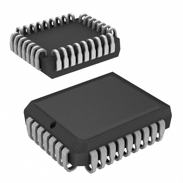


 工商网监
湘ICP备2023018690号
工商网监
湘ICP备2023018690号
