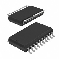
Features
• 80C51 Compatible
•
•
•
•
•
•
•
•
•
•
•
•
•
•
•
– Two I/O Ports
– Two 16-bit Timer/Counters
– 256 bytes RAM
4 Kbytes ROM or 4 Kbytes Flash Program Memory
256 bytes EEPROM (Stack Die Packaging Technology on SO20 Package)
X2 Speed Improvement Capability (6 Clocks/Machine Cycle)
10-bit, 6 Channels A/D Converter
– One-channel with Progammable Gain and Rectifying Amplifier (Accuracy +/- 5%)
– Voltage Reference for A/D & External Analog
Hardware Watchdog Timer
Programmable I/O Mode: Standard C51, Input Only, Push-pull, Open Drain
Asynchronous Port Reset
Triple System Clock
– Crystal or Ceramic Oscillator (24 MHz)
– RC Oscillator (12 MHz), with Calibration Factor Using External R and C
(Accuracy +/- 3.5% with Ideal R and C)
– RC Oscillator, Low Power Consumption (12 MHz Low Accuracy)
– Programmable Prescaler
One PWM Unit Block With:
– 16-bits Programmable Counter
– 3 Independent Modules
One PWM Unit Block with:
– 16 bits Programmable Counter
– 1 Module
Interrupt Structure With:
– 7 Interrupt Sources,
– 4 interrupt Priority Levels
Power Control Modes:
– Idle Mode
– Power-down Mode
– Power Fail Detect, Power On Reset
– Quiet mode for A to D Conversion
Power Supply: 3 to 3.6V
Temperature Range: -40 to 85o C
Package: SO20, SO24 (upon request)
Low-pin-count
8-bit
microcontroller
with A/D
converter
AT83EB5114
AT89EB5114
Description
The AT8xEB5114 is a high performance version of the 80C51 8-bit microcontroller in a
Low Pin Count package.
The AT8xEB5114 retains all the features of the standard 80C51 with 4 Kbytes program memory, 256 bytes of internal RAM, a 7-source, 4-level interrupt system, an onchip oscillator and two timers/counters. AT8xEB5114 may include a serial two wire
interface EEPROM housed together with the microcontroller die in the same package.
The AT8xEB5114 is dedicated for analog interfacing applications. For this, it has a 10bit, 6 channels A/D converter and two PWM units; these PWM blocks provide PWM
generation with variable frequency and pulse width.
In addition, the AT8xEB5114 has a Hardware Watchdog Timer and an X2 speed
improvement mechanism. The X2 feature allows to keep the same CPU power at a
divided by two oscillator frequency. The prescaler allows to decrease CPU and peripherals clock frequency. The fully static design of the AT8xEB5114 allows to reduce
system power consumption by bringing the clock frequency down to any value, even
DC, without loss of data.
Rev. 4311C–8051–02/08
1
�The AT8xEB5114 has 3 software-selectable modes of reduced activity for further reduction in power consumption. In idle mode the CPU is frozen while the peripherals are still
operating. In quiet mode, only the A/D converter is operating. In power-down mode the
RAM is saved and all other functions are inoperative. Three oscillator sources, crystal,
precision RC and low power RC, provide versatile power management.
The AT8xEB5114 is available in low pin count packages (ROM and flash versions).
(3) (2)
XTAL1
XTAL2
R
C
Xtal
Osc
ROM
4 K *8
or
Flash/EE 4K*8
RAM
256
x8
PWMU0
W1M0
W1CI
W0M0-2
W0CI
Vssa
Vcca
Vss
Vcc
Figure 1. Block Diagram
(3) (2)
PWMU1
Watch
Dog
IB-bus
RC
Osc
(12 MHz)
CPU
Timer 0
Timer 1
RC
Osc
(12 MHz)
INT
Ctrl
Vref
Generator
Parallel I/O Ports
A/D
Converter
Port 3 Port 4
X1-20
EEPROM
256 b
2 wires
interface
(SO20)
(3): Alternate function of Port 4
2
P4.0-3
AIN3
P3.0-5(SO20) or 7(SO24)
(2): Alternate function of Port 3
AIN0-2,4-5
(2,3)(3)
Vref
INT1
(2) (3)
INT0
T0
RST
ALE
T1
(2) (3)
(2)
AT89/83EB5114
4311C–8051–02/08
�AT89/83EB5114
Pin Configuration
P4.0/AIN0/W0CI
P4.1/AIN1/T1
P4.2/AIN2/W1CI
P4.3/AIN3/INT1
P3.3/W0M2/AIN4
P3.4/T0/AIN5
P3.5/W1M0
P3.2/INT0
P3.1/W0M1
P3.0/W0M0
1
2
3
4
5
6
7
8
9
10
20
19
18
17
SO20
16
15
14
13
12
11
VRef
Vcca
Vssa
R
C
XTAL2
XTAL1
RST
Vss
Vcc
P4.0/AIN0/W0CI
P4.1/AIN1/T1
P4.2/AIN2/W1CI
P4.3/AIN3/INT1
P3.3/W0M2/AIN4
P3.4/T0/AIN5
1
2
3
4
5
6
7
8
P3.6
P3.5/W1M0
P3.2/INT0 9
P3.1/W0M1 10
P3.0/W0M0 11
P3.7 12
24
23
22
21
SO24
No EE
20
19
18
17
16
15
14
13
VRef
Vcca
Vssa
NC
R
C
XTAL2
XTAL1
NC
RST
Vss
Vcc
3
4311C–8051–02/08
�Pin Description
SO20
SO24
Mnemonic
Type
Name and Function
12
14
VSS
Power
Ground: 0V reference
18
22
Vssa
Power
Analog Ground: 0V reference for analog part
11
13
VCC
Power
Power Supply: This is the power supply voltage for normal, idle and power-down operation.
19
23
Vcca
Power
20
24
VREF
Analog
VREF: A/D converter positive reference input, output of the internal voltage reference
14
17
XTAL1
I
Input to the inverting oscillator amplifier and input to the internal clock generator circuit
15
18
XTAL2
O
Output from the inverting oscillator amplifier. This pin can’t be connected to the ground.
17
20
R
Analog
Resistor Input for the precision RC oscillator
16
19
C
Analog
Capacitor Input for the precision RC oscillator
13
15
RST
I/O
P3.0-P3.7
I/O
Analog Power Supply: This is the power supply voltage for analog part
This pin must be connected to power supply.
Reset input with integrated pull-up
A low level on this pin for two machine cycles while the oscillator is running, resets the device.
Port 3: Port 3 is an 8-bit programmable I/O port with internal pull-ups. See “Port Types” on
page 32. for a description of I/O ports.
Port 3 also serves the special features of the 80C51 family, as listed below.
10
11
I/O
W0M0 (P3.0): External I/O for PWMU 0 module 0
9
10
I/O
W0M1 (P3.1): External I/O for PWMU 0 module 1
8
9
I/O
INT0 (P3.2): External interrupt 0
5
5
I/O
W0M2 / AIN4 (P3.3): External I/O for PWMU 0 module 2. P3.3 is also an input of the analog to
digital converter.
6
6
I/O
T0 / AIN5(P3.4): Timer 0 external input. P3.4 is also an input of the analog to digital converter.
7
8
I/O
W1M0 (P3.5): External I/O for PWMU 1 module 0, can also be used to output the external
clocking signal
P4.0-P4.3
I/O
Port 4: Port 4 is an 4-bit programmable I/O port with internal pull-ups. See “Port Types” on
page 32. for a description of I/O ports.
Port 4 is also the input port of the Analog to digital converter
4
1
1
I/O
2
2
I/O
3
3
I/O
4
4
I/O
AIN0 (P4.0): A/D converter input 0
W0CI: Count input of PWMU0
AIN1 (P4.1): A/D converter input 1
T1: Timer 1 external input
AIN2 (P4.2): A/D converter input 2
W1CI: Count input of PWMU1
AIN3 (P4.3): A/D converter input 3, programmable gain
INT1: External interrupt 1
AT89/83EB5114
4311C–8051–02/08
�AT89/83EB5114
SFR Mapping
The Special Function Registers (SFRs) of the AT8xEB5114 belong to the following
categories:
•
C51 core registers: ACC, AUXR, AUXR1, B, DPH, DPL, PSW, SP, FCON, HSB
•
I/O port registers: P3, P4, P3M1, P3M2, P4M1
•
Timer registers: TCON, TH0, TH1, TL0, TL1, TMOD
•
Power and clock control registers: CKCON, CKRL, CKSEL, OSCBFA, OSCCON,
PCON
•
Interrupt system registers: IEN0, IPH0, IPL0, IOR
•
WatchDog Timer: WDTRST, WDTPRG
•
PWM0 registers: W0CH, W0CL, W0CON, W0FH, W0FL, W0IC, W0MOD, W0R0H,
W0R0L, W0R1H, W0R1L,W0R2H, W0R2L
•
PWM1registers: W1CH, W1CL, W1CON, W1FH, W1FL, W1IC, W1R0H, W1R0L
•
ADC registers: ADCA, ADCF, ADCLK, ADCON, ADDH, ADDL
5
4311C–8051–02/08
�Table 1. SFR Addresses and Reset Values
0/8
F8h
F0h
E8h
E0h
2/A
3/B
4/C
5/D
6/E
W1CON
W1FH
W1FL
W1CH
W1CL
XXX0 0000
0000 0000
0000 0000
0000 0000
0000 0000
W1IC
0000 0000
B
0000 0000
ADCLK
ADCON
0000 0000
0000 0000
ADDL
XXXXXX00
ADDH
0000 0000
ADCF
0000 0000
7/F
FFh
ADCA
0000 0000
W0CON
W0MOD
W0FH
W0FL
W0CH
W0CL
W0IC
HSB
00XX 0000
00XX X000
0000 0000
0000 0000
0000 0000
0000 0000
0000 0000
1111 XX11
ACC
0000 0000
D8h
D0h
1/9
PSW
0000 0000
C8h
P3M2
0000 0000
W0R0H
W0R0L
W0R1H
W0R1L
W0R2H
W0R2L
0000 0000
0000 0000
0000 0000
0000 0000
0000 0000
P3M1
0000 0000
P4M1
0000 0000
FCON
W1R0H
W1R0L
0000 0000
0000 0000
EFh
E7h
0000 0000
1111 1111
F7h
DF
h
D7h
CF
h
C0h
P4
XXXX 1111
C7h
B8h
IPL0
X000 0000
BFh
B0h
P3
1111 1111
A8h
IEN0
0000 0000
IPH0
X000 0000
AFh
AUXR1
XXXX 0XX0
A0h
IOR
WDTRST
XXXXXX00
XXXXXXXX
98h
TCON
0000 0000
0/8
6
A7h
OSCBFA
0111 0110
9Fh
XXXX 1000
80h
Note:
WDTPRG
XXXX X000
CKRL
90h
88h
B7h
TMOD
0000 0000
TL0
0000 0000
TL1
0000 0000
SP
0000 0111
DPL
0000 0000
DPH
0000 0000
1/9
2/A
3/B
TH0
0000 0000
TH1
0000 0000
AUXR
0XX0 XXX0
CKCON
XXXX XXX0
CKSEL
XXXX XXCC
OSCCON
XXXX XXCC
00XX XX00
5/D
6/E
7/F
4/C
PCON
97h
8Fh
87h
1. "C", value defined by the Hardware Security Byte, see Table 2 on page 15
AT89/83EB5114
4311C–8051–02/08
�AT89/83EB5114
Mnemonic
Add
Name
7
6
5
4
3
2
1
0
ACC
E0h
Accumulator
ADCA
F7h
ADC Amplifier Configuration
-
-
-
-
-
AC3E
AC3G1
AC3G0
ADCF
F6h
ADCF Register
-
-
CH5
CH4
CH3
CH2
CH1
CH0
ADCLK
F2h
ADC Clock Prescaler
SELREF
PRS6
PRS5
PRS4
PRS3
PRS2
PRS1
PRS0
ADCON
F3h
ADC Control Register
QUIETM
PSIDLE
ADEN
ADEOC
ADSST
SCH2
SCH1
SCH0
ADDH
F5h
ADC Data High Byte Register
ADAT9
ADAT8
ADAT7
ADAT6
ADAT5
ADAT4
ADAT3
ADAT2
ADDL
F4h
ADC Data Low Byte Register
-
-
-
-
-
-
ADAT1
ADAT0
AUXR
8Eh
Auxiliary Register
DPU
-
-
LOWVD
-
-
-
-
AUXR1
A2h
Auxiliary Register 1
-
-
-
-
-
-
-
DPS
B
F0h
B Register
CKCON
8Fh
Clock control Register
-
-
-
-
-
-
-
X2
CKRL
97h
Clock Prescaler Register
-
-
-
-
CKRL3
CKRL2
CKRL1
CKRL0
CKSEL
85h
Clock Selection register
-
-
-
-
-
-
CKS1
CKS0
DPH
83h
Data pointer High Byte
DPL
82h
Data pointer Low Byte
FCON
D1h
Auxiliary Register
FPL3
FPL2
FPL1
FPL0
FPS
FMOD1
FMOD0
FBUSY
HSB
EFh
Hardware Security Byte
X2
RST_OSC1
RST_OSC0
RST_OCLK
-
-
LB1
LB0
IEN0
A8h
Interrupt Enable Register
EA
EADC
EW1
EW0
ET1
EX1
ET0
EX0
IOR
A5h
Interrupt Option Register
-
-
-
-
-
-
ESB1
ESB0
IPH0
B7h
Interrupt Priority register
-
PADCH
PW1H
PW0H
PT1H
PX1H
PT0H
PX0H
IPL0
B8h
Interrupt Priority Register
-
PADC
PW1
PW0
PT1
PX1
PT0
PX0
OSCBFA
9Fh
Oscillator B Frequency Adjust
OSCBFA7
OSCBFA6
OSCBFA5
OSCBFA4
OSCBFA3
OSCBFA2
OSCBFA1
OSCBFA0
OSCCON
86h
Clock Control Register
-
-
-
OSCBRY
LCKEN
OSCCEN
OSCBEN
OSCAEN
P3
B0h
Port 3 Register
P3M1
D5h
Port 3 Output Configuration
P3M1.7
P3M1.6
P3M1.5
P3M1.4
P3M1.3
P3M1.2
P3M1.1
P3M1.0
P3M2
E4h
Port 3 Output Configuration
P3M2.7
P3M2.6
P3M2.5
P3M2.4
P3M2.3
P3M2.2
P3M2.1
P3M2.0
P4
C0h
Port 4 register
P4M1
D6h
Port 4 Output Configuration
P4M1.7
P4M1.6
P4M1.5
P4M1.4
P4M1.3
P4M1.2
P4M1.1
P4M1.0
PCON
87h
Power Modes Control Register
SMOD1
SMOD0
-
-
GF1
GF0
PD
IDL
PSW
D0h
Program Status Word
CY
AC
F0
RS1
RS0
OV
F1
P
SP
81h
Stack pointer
TCON
88h
Timer/Counter Control Register
TF1
TR1
TF0
TR0
IE1
IT1
IE0
IT0
TH0
8Ch
Timer 0 High Byte Registers
TH0.7
TH0.6
TH0.5
TH0.4
TH0.3
TH0.2
TH0.1
TH0.0
TH1
8Dh
Timer 1 High Byte Registers
TH1.7
TH1.6
TH1.5
TH1.4
TH1.3
TH1.2
TH1.1
TH1.0
TL0
8Ah
Timer 0 Low Byte Registers
TL0.7
TL0.6
TL0.5
TL0.4
TL0.3
TL0.2
TL0.1
TL0.0
TL1
8Bh
Timer 1 Low Byte Registers
TL1.7
TL1.6
TL1.5
TL1.4
TL1.3
TL1.2
TL1.1
TL1.0
7
4311C–8051–02/08
�Mnemonic
8
Add
Name
7
6
5
4
3
2
1
0
TMOD
89h
Timer/Counter Mode Register
GATE1
C/T1#
M11
M01
GATE0
C/T0#
M10
M00
W0CH
ECh
PWMU0 Counter High Control
W0C15
W0C14
W0C13
W0C12
W0C11
W0C10
W0C9
W0C8
W0CL
EDh
PWMU0 Counter Low Control
W0C7
W0C6
W0C5
W0C4
W0C3
W0C2
W0C1
W0C0
W0CON
E8h
PWMU0 Control Register
W0UP
W0R
-
-
W0OS
W0EN2
W0EN1
W0EN0
W0FH
EAh
PWMU0 Frequency High
Control
W0F15
W0F14
W0F13
W0F12
W0F11
W0F10
W0F9
W0F8
W0FL
EBh
PWMU0 Frequency Low
Control
W0F7
W0F6
W0F5
W0F4
W0F3
W0F2
W0F1
W0F0
W0IC
EEh
PWMU0 Interrupt Configuration
W0CF
W0CF2
W0CF2
W0CF0
W0ECF
W0ECF2
W0ECF1
W0ECF0
W0MOD
E9h
PWMU0 Counter Mode
Register
W0CPS1
W0CPS0
-
-
-
W0INV2
W0INV1
W0INV0
W0R0H
D9h
PWMU0 Module 0 High Toggle
W0R0H15
W0R0H14
W0R0H13
W0R0H12
W0R0H11
W0R0H10
W0R0H9
W0R0H8
W0R0L
DAh
PWMU0 Module 0 Low Toggle
W0R0H7
W0R0H6
W0R0H5
W0R0H4
W0R0H3
W0R0H2
W0R0H1
W0R0H0
W0R1H
DBh
PWMU0 Module 1High Toggle
W0R1H15
W0R1H14
W0R1H13
W0R1H12
W0R1H11
W0R1H10
W0R1H9
W0R1H8
W0R1L
DCh
PWMU0 Module1 Low Toggle
W0R1H7
W0R1H6
W0R1H5
W0R1H4
W0R1H3
W0R1H2
W0R1H1
W0R1H0
W0R2H
DDh
PWMU0 Module 2 High Toggle
W0R2H15
W0R2H14
W0R2H13
W0R2H12
W0R2H11
W0R2H10
W0R2H9
W0R2H8
W0R2L
DEh
PWMU0 Module 2 Low Toggle
W0R2H7
W0R2H6
W0R2H5
W0R2H4
W0R2H3
W0R2H2
W0R2H1
W0R2H0
W1CH
FCh
PWMU1 Counter High Control
W1C15
W1C14
W1C13
W1C12
W1C11
W1C10
W1C9
W1C8
W1CL
FDh
PWMU1 Counter Low Control
W1C7
W1C6
W1C5
W1C4
W1C3
W1C2
W1C1
W1C0
W1CON
F8h
PWMU1 Control Register
W1UP
W1R
-
W1OCLK
W1CPS1
W1CPS0
W1INV0
W1EN0
W1FH
FAh
PWMU1 Frequency High
Control
W1F15
W1F14
W1F13
W1F12
W1F11
W1F10
W1F9
W1F8
W1FL
FBh
PWMU1 Frequency Low
Control
W1F7
W1F6
W1F5
W1F4
W1F3
W1F2
W1F1
W1F0
W1IC
FEh
PWMU1 Interrupt Configuration
W1CF
-
-
W1CF0
W1ECOF
-
-
W0ECF0
W1R0H
C9h
PWMU1 Module 0 High Toggle
W1R0H15
W1R0H14
W1R0H13
W1R0H12
W1R0H11
W1R0H10
W1R0H9
W1R0H8
W1R0L
CAh
PWMU1 Module 0 Low Toggle
W1R0H7
W1R0H6
W1R0H5
W1R0H4
W1R0H3
W1R0H2
W1R0H1
W1R0H0
WDTRST
A6h
Watchdog Timer enable
Register
WDTPRG
A7h
WatchDog Timer Duration Prg
-
-
-
-
-
S2
S1
S0
AT89/83EB5114
4311C–8051–02/08
�AT89/83EB5114
Power Monitor
The Power Monitor function supervises the evolution of the voltages feeding the microcontroller, and if needed, suspends its activity when the detected value is out of
specification.
It warrants proper startup when AT8xEB5114 is powered up and prevents code execution errors when the power supply becomes lower than the functional threshold.
This chapter describes the functions of the power monitor.
Description
In order to startup and to properly maintain the microcontroller operation, Vcc has to be
stabilized in the Vcc operating range and the oscillator has to be stabilized with a nominal amplitude compatible with logic threshold.
In order to be sure the oscillator is stabilized, there is an internal counter which maintains the reset during 1024 clock periods in case the oscillator selected is the OSC A
and 64 clock periods in case the oscillator used is OSC B or OSC C.
This control is carried out during three phases: the power-up, normal operation and
stop. In accordance with the following requirements:
•
it guarantees an operational Reset when the microcontroller is powered-up, and
•
a protection if the power supply goes below minimum operating Vcc
Figure 2. Power Monitor Block Diagram
External
Vcc
Power-Supply
Power up
Detector
Power Monitor diagram
Power Fail
Detector
Internal RESET
The Power Monitor monitors the power-supply in order to detect any voltage drops
which are not in the target specification. The power monitor block verifies two kinds of
situation that may occur:
•
during the power-up condition, when Vcc reaches the product specification,
•
during a steady-state condition, when Vcc is at nominal value but disturbed by any
undesired voltage drops.
Figure 2 shows some configurations which can be handled by the Power Monitor.
9
4311C–8051–02/08
�Figure 3. Power-Up and Steady-state Conditions Monitored
Vcc
VPFDP
VPFDM
tG
tR
t
Power-up
Steady State Condition
Reset
Vcc
The POR/PFD forces the CPU into reset mode when VCC reaches a voltage condition
which is out of specification.
The thresholds and their functions are:
•
VPFDP: the Vcc has reached a minimum functional value at power-up. The circuit
leaves the RESET mode
•
VPFDM: the Vcc has reached a low threshold functional value for the
microcontroller. An internal RESET is set.
Glitch filtering prevents the system from RESET when short duration glitches are carried
on Vcc power-supply (See “Electrical Characteristics” on page 84.).
In case Vcc is below VPFDP, LOWVD bit in AUXR (See Table 12 on page 23) is cleared
by hardware. This bit allows the user to know if the voltage is below VPFDP.
Note: For proper reset operation VCCA and V CC must be considered together (same
power source). However, to improve the noise immunity, it is better to have two decoupling networks close to power pins (one for VCCA/VSSA pair and one for VCC/VSS pair).
10
AT89/83EB5114
4311C–8051–02/08
�AT89/83EB5114
Clock System
The AT8xEB5114 oscillator system provides a reliable clocking system with full mastering of speed versus CPU power trade-off. Several clock sources are possible:
Overview
•
External clock input
•
High speed crystal or ceramic oscillator
•
Integrated accurate oscillator with external R and C.
•
Low power consumption Integrated RC oscillator without external components.
The AT8xEB5114 needs 6 clock periods per machine cycle when the X2 function is set.
However, the selected clock source can be divided by 2-32 before clocking the CPU and
the peripherals.
By default, the active oscillator after reset is the high speed crystal/ceramic oscillator.
Any two bits in a hardware configuration byte programmed by a Flash programmer or by
metal mask can activate any other one.
The clock system is controlled by several SFR registers: CKCON, CKSEL, CKRL,
OSCON, PCON and HSB which is the hardware security byte.
The AT8xEB5114 includes three oscillators:
Blocks Description
•
Crystal oscillator optimized for 24 MHz.
•
1 accurate oscillator with a typical frequency of 12 MHz.
•
1 low power oscillator with a typical frequency of 14 MHz.
Figure 4. Functional Block Diagram
CKRL
A/D Clock
Xtal1
Xtal_Osc
OSCA
Xtal2
11
10
OSCAEN
OSCBEN
PwdOsc
RC_Osc
OSCB
R
C
Freq. Adjust
Mux
01 +
Filter
CkAdc
OscOut
2 down to 32
Prescaler-Divider
0
CkOut
CkIdle
1
CPU Clock
CKS
OSCBRY
Peripherals Clock
X2
Ck
LCKEN
Quiet Pwd Idle
RC_Osc
OSCC
OSCCEN
11
4311C–8051–02/08
�Crystal Oscillator: OSCA
The crystal oscillator uses two external pins, XTAL1 for input and XTAL2 for output.
OSCAEN in OSCCON register is an enable signal for the crystal oscillator or for the
external oscillator input that can be provided on XTAL1.
High Accurate RC Oscillator:
OSCB
The high accuracy RC oscillator needs external R and C components to assure the
proper accuracy; its typical frequency is 12 MHz. Frequency accuracy is a function of
external R and C accuracy. It is recommended to use 0.5% or better for R and 1% for C
components. (Typical values are R = 49.9 K and C = 560 pF)
This oscillator has two modes.
•
OSCBEN = 1 and LCKEN = 0: Standard accuracy mode(Typical frequency 12 MHz)
•
OSCBEN = 1 and LCKEN = 1: High accuracy mode (Typical frequency 12 MHz).
The OSCB oscillator is based on a low frequency RC oscillator and a VCO. When
locked, the oscillator frequency is defined by the following formula:
F = 3*[OSCBFA+1]/(R.C). with C including parasitic capacitances.
Because the oscillator is based on a PLL, it needs several periods to reach its final
accuracy. As soon as this accuracy is reached, the OSCBRY bit in OSCCON
register is set by hardware.
The internal frequency is locked on the external RC time constant. So it is possible
to adjust frequency by lower than 1% steps with the OSCBFA register. However the
frequency adjustment is limited to +/-15% around 12 MHz.
The frequency can be adjusted until 15% around 12 MHz by OSCBFA Register.
OSCBEN and LCKEN are in the OSCCON register.
Low Power Consumption
Oscillator: OSCC
The low power consumption RC oscillator doesn’t need any external components. Moreover its consumption is very low. Its typical frequency is 14 MHz. Note that this on-chip
oscillator has a +/- 40% frequency tolerance and may not be suitable for use in certain
applications.
OSCC is set by OSCCEN bit in OSCCON.
Clock Selector
CKS1 and CKS0 bits in CKSEL register are used to select the clock source.
OSCCEN bit in OSCCON register is used to enable the low power consumption RC
oscillator.
OSCBEN bit in OSCCON register is used to enable the high accurate RC oscillator.
OSCAEN bit in OSCCON register is used to enable the crystal oscillator or the external
oscillator input.
X2 Feature
The AT8xEB5114 core needs only 6 clock periods per machine cycle. This feature
called ”X2” provides the following advantages:
•
Divides frequency crystals by 2 (cheaper crystals) while keeping same CPU power.
•
Saves power consumption while keeping same CPU power (oscillator power
saving).
•
Saves power consumption by dividing dynamically the operating frequency by 2 in
operating and idle modes.
•
Increases CPU power by 2 while keeping same crystal frequency.
In order to keep the original C51 compatibility, a divider by 2 is inserted between the
XTAL1 signal and the main clock input of the core (phase generator). This divider may
be enabled or disabled by software.
12
AT89/83EB5114
4311C–8051–02/08
�AT89/83EB5114
The clock for the whole circuit and peripherals is first divided by two before being used
by the CPU core and the peripherals.
Description
This allows any cyclic ratio to be accepted on XTAL1 input. In X2 mode, as this divider is
bypassed, the signals on XTAL1 must have a cyclic ratio from 40 to 60%.
Figure 4 shows the clock generation block diagram. X2 bit is validated on the rising edge
of the XTAL1÷2 to avoid glitches when switching from X2 to standard mode. Figure 5
shows the switching mode waveforms.
Figure 5. Mode Switching Waveforms
XTAL1
XTAL1:2
X2 bit
FOSC
CPU clock
STD Mode
X2 Mode
STD Mode
The X2 bit in the CKCON register (see Table 7 on page 18) allows to switch from 12
clock periods per instruction to 6 clock periods and vice versa.
Clock Prescaler
Before supplying the CPU and the peripherals, the main clock is divided by a factor from
2 to 32, as defined by the CKRL register (see Table 6 on page 18). The CPU needs from
12 to 16*12 clock periods per instruction. This allows:
•
to accept any cyclic ratio on XTAL1 input.
•
to reduce CPU power consumption.
Note:
Prescaler Divider on Reset
The number of bits of the prescaler is optimized in order to provide a low power consumption in low speed mode (see Section “Electrical Characteristics”, page 84).
A hardware RESET selects the start oscillator depending on the RST1_OSC and
RST0_OSC bits contained on the Hardware Security Byte register (see Table 2 on page
15). It also selects the prescaler divider as follows:
•
CKRL = 8h: internal clock = OscOut / 16 (slow CPU speed at reset, thus lower
power consumption)
•
X2 = 0,
•
SEL_OSC1 and SEL_OSC0 bits selects OSCA, OSCB or OSCC, depending on the
value of the RST_OSC1 and RST_OSC0 configuration bits.
•
After Reset, any value between Fh down to 0h can be written by software into CKRL
sfr in order to divide frequency of the selected oscillator:
–
CKRL = 0h: minimum frequency = OscOut / 32
–
CKRL = Fh: maximum frequency = OscOut / 2
The frequency of the CPU and peripherals clock CkOut is related to the frequency of the
main oscillator OscOut by the following formula:
FCkOut = FOscOut / (32 - 2*CKRL)
13
4311C–8051–02/08
�Some examples can be found in the table below:
FOscOut
•
14
FCkOut
MHz
X2
CKRL
Mhz
12
0
F
6
12
0
E
3
12
1
x
12
A software instruction which set X2 bit disables the prescaler/divider, so the internal
clock is either OSCA, OSCB or OSCC depending on SEL_OSC1 and SEL_OSC0
bits.
AT89/83EB5114
4311C–8051–02/08
�AT89/83EB5114
Registers
Hardware Security Byte
The security byte sets the starting microcontroller options and the security levels.
The default options are X1 mode, Oscillator A and divided by 16 prescaler.
Table 2. Hardware Security Byte (HSB)
Power configuration Register - HSB (S:EFh)
7
X2
6
5
4
RST_OSC1 RST_OSC0 RST_OCLK
Bit
Bit
Number
Mnemonic
7
X2
3
2
1
0
CKRLRV
-
LB1
LB0
Description
X2 Mode
Clear to force X2 mode (CkOut = OscOut)
Set to use the prescaler mode (CkOut = OscOut / (2*(16-M)))
6
RST_OSC1
Oscillator bit 1 on reset and Oscillator bit 0 on reset
11: allows OSCA
10: allows OSCB
5
RST_OSC0
01: allows OSCC
00: reserved
Output clocking signal after RESET
4
RST_OCLK
Clear to start the microcontroller with a low level on P3.5 followed by an output
clocking signal on P3.5 as soon as the microcontroller is started. This signal has
is a 1/3 high 2/3 low signal. Its frequency is equal to (CKout / 3).
Set to start on normal conditions: No signal on P3.5 which is pulled up.
CKRL Reset Value
3
CKRLRV
If set, the microcontroller starts with the prescaler reset value = XXXX 1000
(OscOut = CkOut/16).
If clear, the microcontroller starts with a prescaler reset value = XXXX 1111
(OscOut = CkOut/2).
2
-
1-0
LB1-0
Reserved
User Program Lock Bits
See Table 61 on page 81
HSB = 1111 1X11b
15
4311C–8051–02/08
�Clock Control Register
The clock control register is used to define the clock system behavior.
Table 3. OSCON Register
OSCCON - Clock Control Register (86h)
7
6
5
4
3
2
1
0
-
-
OSCARY
OSCBRY
LCKEN
OSCCEN
OSCBEN
OSCAEN
Bit
Bit
Number
Mnemonic
7
-
Reserved
The value read from this bit is indeterminate. Do not set this bit.
6
-
Reserved
The value read from this bit is indeterminate. Do not set this bit.
5
OSCARY
4
OSCBRY
3
LCKEN
Description
Oscillator A Ready
When set, this bit indicates that Oscillator A is ready to be used.
Oscillator B Ready
When set, this bit indicates that Oscillator B is ready to be used in high accurate
mode.
Lock Enable
2
OSCCEN
When set, this bit allows to increase the accuracy of OSCB by locking this
oscillator on external RC time constant.
Enable low power consumption RC oscillator
This bit is used to enable the low power consumption oscillator
0: The oscillator is disabled
1: The oscillator is enabled.
1
OSCBEN
Enable high accuracy RC oscillator
This bit is used to enable the high accurate RC oscillator
0: The oscillator is disabled
1: The oscillator is enabled.
0
OSCAEN
Enable crystal oscillator
This bit is used to enable the crystal oscillator
0: The oscillator is disabled
1: The oscillator is enabled.
Reset Value = XXX0
0"RST_OSC1.RST_OSC0""RST_OSC1.RST_OSC0""RST_OSC1.RST_OSC0" b
Not bit addressable
Note:
Oscillator B Frequency Adjust
Register
16
Before changing oscillator selection in CKSEL, be sure that the oscillator you select is
started. OSCA is ready as soon as OSCARY is set by hardware, OSCB and OSCC are
ready after 4 clock periods. In case you want to use OSCB locked, be sure that OSCB is
started before setting LCKEN bit. Then, wait until OSCBRY is set by hardware to be sure
that the accurate frequency is reached.
The OSCB Frequency Adjust register is used to adjust the frequency in case of external
components inaccuracies. It allows a frequency variation about 15% around 12 MHz
with a step of around 1%.
AT89/83EB5114
4311C–8051–02/08
�AT89/83EB5114
Table 4. OSCBFA Register
OSCBFA- Oscillator B Frequency Adjust Register (9Fh)
7
6
5
4
3
2
1
0
OSCBFA7
OSCBFA6
OSCBFA5
OSCBFA4
OSCBFA3
OSCBFA2
OSCBFA1
OSCBFA0
Bit
Bit
Number
Mnemonic
7-0
OSCBFA
7-0
Description
OSCB Frequency adjust
The reset value to have 12 MHz is 0111 0110. It is possible to modify this value
in order to increase or decrease the frequency.
Reset Value = 0111 0110b
Not bit addressable
Clock Selection Register
The clock selection register is used to define the clock system behavior.
Table 5. CKSEL Register
CKSEL - Clock Selection Register (85h)
7
6
5
4
3
2
1
0
-
-
-
-
-
-
CKS1
CKS0
Bit
Bit
Number
Mnemonic
7
-
Reserved
The value read from this bit is indeterminate. Do not set this bit.
6
-
Reserved
The value read from this bit is indeterminate. Do not set this bit.
5
-
Reserved
The value read from this bit is indeterminate. Do not set this bit.
4
-
Reserved
The value read from this bit is indeterminate. Do not set this bit.
3
-
Reserved
The value read from this bit is indeterminate. Do not set this bit.
2
-
Reserved
The value read from this bit is indeterminate. Do not set this bit.
1
CKS1
Description
Active Clock Selector 1and Active Clock Selector 0
These bits are used to select the active oscillator
11: The crystal oscillator is selected
0
CKS0
10: The high accuracy RC oscillator is selected
01: The low power consumption RC oscillator is selected
00: Reserved
Reset Value = XXXX XX"RST_OSC1" "RST_OSC0" b
Not bit addressable
17
4311C–8051–02/08
�Clock Prescaler Register
This register is used to reload the clock prescaler of the CPU and peripheral clock.
Table 6. CKRL Register
CKRL - Clock prescaler Register (97h)
7
6
5
4
-
-
-
-
Bit
Number
3
2
1
0
M
Bit
Mnemonic Description
7-4
-
3-0
CKRL
Reserved
0000b: Division factor equal 32
1111b: Division factor equal 2
M: Division factor equal 2*(16-M)
Reset Value = XXXX 1000b
Not bit addressable
Clock Control Register
This register is used to control the X2 mode of the CPU and peripheral clock.
Table 7. CKCON Register
CKCON - Clock Control Register (8Fh)
7
6
5
4
3
2
1
0
-
-
-
-
-
-
-
X2
Bit
Bit
Number
Mnemonic
7-1
-
0
X2
Description
Reserved
X2 Mode
Set to force X2 mode (CkOut = OscOut)
Clear to use the prescaler mode (CkOut = OscOut / (2*(16-M)))
Reset Value = 0000 0000b
Not bit addressable
18
AT89/83EB5114
4311C–8051–02/08
�AT89/83EB5114
Power Modes
Overview
As seen in the previous chapter it is possible to modify the AT8xEB5114 clock management in order to have less consumption.
For applications where power consumption is a critical factor, three power modes are
provided:
•
Normal (running) mode
•
Idle mode
•
Power-down mode
In order to increase ADC accuracy, a Quiet mode also exits. This mode is a pseudo idle
mode in which the CPU and all the peripherals except the AD converter are disabled.
Power modes are controlled by PCON SFR register.
Operating Modes
Table 8 summarizes all the power modes and states that AT8xEB5114 can encounter. It
shows which parts of AT8xEB5114 are running depending on the operating mode.
Table 8. Operating Modes
Operating Mode
Prescaler
Oscillator
POR
Power Down
Peripherals
X
Under Reset
Normal Mode
CPU
A, B or C
X
Start
X
A, B or C
X
X
Running
(X)
A, B or C
X
X
Idle
(X)
A, B or C
X
X
Quiet
(X)
A, B or C
X
only ADC
X
In normal mode, the oscillator, the CPU and the peripherals are running. The prescaler
can also be activated.
•
The CPU and the peripherals clock depends on the software selection using
CKCON, OSCCON, CKSEL and CKRL registers
•
CKS bits select either OSCA, OSCB, or OSCC
•
CKRL register determines the frequency of the selected clock, unless X2 bit is set.
In this case the prescaler/divider is not used, so CPU core needs only 6-clock
periods per machine cycle.
It is always possible to switch dynamically by software from one to another oscillator by
changing CKS bits, a synchronization cell allows to avoid any spike during transition.
Idle Mode
The idle mode allows to reduce consumption by freezing the CPU. All the peripherals
continue running.
Entering Idle Mode
An instruction that sets PCON.0 causes that to be the last instruction executed before
going into Idle mode.
In Idle mode, the internal clock signal is gated off to the CPU, but not to the interrupt,
and the peripheral functions. The CPU status is entirely preserved: the Stack Pointer,
Program Counter, Program Status Word, Accumulator and all other registers maintain
19
4311C–8051–02/08
�their data during Idle. The port pins hold the logical states they had at the time Idle was
activated. ALE and PSEN are held at logic high levels. The different operating modes
are summarized on Table 10 on page 21.
There are two ways to terminate idle mode. Activation of any enabled interrupt will
cause PCON.0 to be cleared by hardware, terminating Idle mode. The interrupt will be
serviced, and following RETI the next instruction to be executed will be the one following
the instruction that put the device into idle. Exit from idle mode will leave the oscillators
control bits on OSCON and CKS registers unchanged.
Exit from Idle Mode
The flag bits GF0 and GF1 can be used to give an indication if an interrupt occurred during normal operation or during an Idle mode. For example, an instruction that activates
Idle mode can also set one or both flag bits. When Idle is terminated by an interrupt, the
interrupt service routine can examine the flag bits.
The other way of terminating the Idle mode is with a hardware reset. Since the clock
oscillator is still running, the hardware reset needs to be held active for only two
machine cycles (24 oscillator periods) to complete the reset.
In both cases, PCON.0 is cleared by hardware.
Quiet Mode
The quiet mode is a pseudo idle mode in which the CPU and all the peripherals except
the AD converter are down. For more details, See “Analog-to-Digital Converter (ADC)”
on page 57.
Power-down Mode
To save maximum power, a power-down mode can be invoked by software (refer to
Table 11 on page 22). In power-down mode, the oscillator is stopped and the instruction
that invoked power-down mode is the last instruction executed. The internal RAM and
SFRs retain their value until the power-down mode is terminated. VCC can be lowered to
save further power.
Entering Power-down Mode
An instruction that sets PCON.1 causes that to be the last instruction executed before
going into the power-down mode.
The ports status under power-down is the previous status before entering this power
mode.
Exit from Power-down Mode
Either a hardware reset or an external interrupt (low level) on INT0 or INT1 (if enabled)
can cause an exit from power-down. To properly terminate power-down, the reset or
external interrupt should not be executed before VCC is restored to its normal operating
level and must be held active long enough for the oscillator to restart and stabilize.
Exit from power-down by external interrupt does not affect the SFRs and the internal
RAM content.
Figure 6. Power-down Exit Waveform
INTERRUPT
OSC
Active phase
Power-down phase
Oscillator restart phase
Active phase
By a hardware Reset, the CPU will restart in the mode defined by the RST_OSC1 and
RST_OSC0 bits in HSB.
20
AT89/83EB5114
4311C–8051–02/08
�AT89/83EB5114
By INT1 and INT0 interruptions (if enabled), the oscillators control bits on OSCON and
CKSEL will be kept, so the selected oscillator before entering in power-down mode will
be activated. Only external interrupts INT0 and INT1 are useful to exit from power-down.
Note:
Exit from power down mode doesn’t depend on IT0 and IT1 configurations. It is only possible to exit from power down mode on a low level on these pins.
Holding the pin low restarts the oscillator but bringing the pin high completes the exit as
detailed in Figure 6. When both interrupts are enabled, the oscillator restarts as soon as
one of the two inputs is held low and power down exit will be completed when the first
input is released. In this case the higher priority interrupt service routine is executed.
Table 9 shows the state of ports during idle and power-down modes.
Table 9. Ports State
Mode
Program Memory
Port3
Port4
Idle
Internal
Port Data
Port Data
Power Down
Internal
Port Data
Port Data
Table 10. Operating Modes
PD
IDLE
CKS1
CKS0
OSCCEN
OSCBEN
OSCAEN
Selected Mode
Comment
0
0
1
1
X
X
1
NORMAL MODE A
OSCA: XTAL clock
X
X
1
1
X
X
0
INVALID
no active clock
0
0
1
0
X
1
X
NORMAL MODE B,
OSCB: high accuracy RC clock
X
X
1
0
X
0
X
INVALID
no active clock
0
0
0
1
1
X
X
NORMAL MODE C,
OSCC: low consumption RC clock
X
X
0
1
0
X
X
INVALID
no active clock
0
1
1
1
X
X
1
IDLE MODE A
The CPU is off, OSCA supplies the
peripherals
0
1
1
0
X
1
X
IDLE MODE B
The CPU is off, OSCB supplies the
peripherals
0
1
0
1
1
X
X
IDLE MODE C
The CPU is off, OSCC supplies the
peripherals
1
X
X
X
X
X
X
POWER DOWN
The CPU is off, OSCA, OSCB and
OSCC are stopped
21
4311C–8051–02/08
�Power Modes Control
Registers
Table 11. PCON Register
PCON (S:87h)
Power configuration Register
7
6
5
4
3
2
1
0
-
-
-
-
GF1
GF0
PD
IDL
Bit
Number
Bit
Mnemonic
Description
7
Reserved
6
Reserved
5
Reserved
4
Reserved
3
GF1
General Purpose flag 1
Set and Cleared by user for general purpose usage.
2
GF0
General Purpose flag 0
Set and Cleared by user for general purpose usage.
PD
Power-down Mode bit
Cleared by hardware when an interrupt or reset occurs.
Set to activate the Power-down mode.
If IDL and PD are both set, PD takes precedence.
IDL
Idle Mode bit
Cleared by hardware when an interrupt or reset occurs.
Set to activate the Idle mode.
If IDL and PD are both set, PD takes precedence.
1
0
Reset Value = 00XX XX00b
22
AT89/83EB5114
4311C–8051–02/08
�AT89/83EB5114
AUXR Register
Table 12. AUXR Register
AUXR - Auxiliary Register (8Eh)
7
6
5
4
3
2
1
0
DPU
-
-
LOWVD
-
-
-
-
Bit
Number
7
Bit
Mnemonic Description
DPU
Disable Pull up
Set to disable each pull up on all ports.
Clear to connect all pull-ups on each port.
6
-
Reserved
The value read from this bit is indeterminate. Do not set this bit.
5
-
Reserved
The value read from this bit is indeterminate. Do not set this bit.
4
LOWVD
Low Voltage Detection
This bit is clear by hardware when the supply voltage is under Vpfdp value.
This bit is set by hardware as soon the supply voltage is greater than Vpfdp value.
3-1
-
Reserved
The value read from this bit is indeterminate. Do not set this bit.
0
-
Reserved
The value read from this bit is indeterminate. Do not set this bit.
Reset Value = 0XX0 XXXXb
Not bit addressable
23
4311C–8051–02/08
�Timers/Counters
Introduction
The AT8xEB5114 implements two general-purpose, 16-bit Timers/Counters. Although
they are identified as Timer 0, Timer 1, they can be independently configured each to
operate in a variety of modes as a Timer or as an event Counter. When operating as a
Timer, a Timer/Counter runs for a programmed length of time, then issues an interrupt
request. When operating as a Counter, a Timer/Counter counts negative transitions on
an external pin. After a preset number of counts, the Counter issues an interrupt
request.
The Timer registers and associated control registers are implemented as addressable
Special Function Registers (SFRs). Two of the SFRs provide programmable control of
the Timers as follows:
•
Timer/Counter mode control register (TMOD) and Timer/Counter control register
(TCON) control both Timer 0 and Timer 1.
The various operating modes of each Timer/Counter are described below.
Timer/Counter
Operations
A basic operation is Timer registers THx and TLx (x = 0, 1) connected in cascade to
form a 16-bit Timer. Setting the run control bit (TRx) in the TCON register (see
Figure 15) turns the Timer on by allowing the selected input to increment TLx. When
TLx overflows it increments THx and when THx overflows it sets the Timer overflow flag
(TFx) in the TCON register. Setting the TRx does not clear the THx and TLx Timer registers. Timer registers can be accessed to obtain the current count or to enter preset
values. They can be read at any time but the TRx bit must be cleared to preset their values, otherwise the behavior of the Timer/Counter is unpredictable.
The C/Tx# control bit selects Timer operation or Counter operation by selecting the
divided-down system clock or the external pin Tx as the source for the counted signal.
The TRx bit must be cleared when changing the operating mode, otherwise the behavior
of the Timer/Counter is unpredictable.
For Timer operation (C/Tx# = 0), the Timer register counts the divided-down system
clock. The Timer register is incremented once every peripheral cycle.
For Counter operation (C/Tx# = 1), the Timer register counts the negative transitions on
the external input pin Tx. The external input is sampled during every S5P2 state. The
Programmer’s Guide describes the notation for the states in a peripheral cycle. When
the sample is high in one cycle and low in the next one, the Counter is incremented. The
new count value appears in the register during the next S3P1 state after the transition
has been detected. Since it takes 12 states (24 oscillator periods in X1 mode) to recognize a negative transition, the maximum count rate is 1/24 of the oscillator frequency in
X1 mode. There are no restrictions on the duty cycle of the external input signal, but to
ensure that a given level is sampled at least once before it changes, it should be held for
at least one full peripheral cycle.
Timer 0
Timer 0 functions as either a Timer or an event Counter in four operating modes.
Figure 7 to Figure 10 show the logic configuration of each mode.
Timer 0 is controlled by the four lower bits of the TMOD register (see Figure 16) and bits
0, 1, 4 and 5 of the TCON register (see Figure 15). The TMOD register selects the
method of Timer gating (GATE0), Timer or Counter operation (T/C0#) and the operating
mode (M10 and M00). The TCON register provides Timer 0 control functions: overflow
flag (TF0), run control bit (TR0), interrupt flag (IE0) and interrupt type control bit (IT0).
For normal Timer operation (GATE0= 0), setting TR0 allows TL0 to be incremented by
the selected input. Setting GATE0 and TR0 allows external pin INT0# to control Timer
24
AT89/83EB5114
4311C–8051–02/08
�AT89/83EB5114
operation.
Timer 0 overflow (count rolls over from all 1s to all 0s) sets the TF0 flag and generates
an interrupt request.
It is important to stop the Timer/Counter before changing modes.
Mode 0 configures Timer 0 as a 13-bit Timer which is set up as an 8-bit Timer (TH0 register) with a modulo-32 prescaler implemented with the lower five bits of the TL0 register
(see Figure 7). The upper three bits of the TL0 register are indeterminate and should be
ignored. Prescaler overflow increments the TH0 register.
Mode 0 (13-bit Timer)
Figure 7. Timer/Counter x (x= 0 or 1) in Mode 0
FCkIdle
/6
0
THx
(8 bits)
1
Tx
TLx
(5 bits)
Overflow
TFx
TCON reg
Timer x
Interrupt
Request
C/Tx#
TMOD reg
INTx#
GATEx
TRx
TMOD reg
TCON reg
Mode 1 configures Timer 0 as a 16-bit Timer with the TH0 and TL0 registers connected
in a cascade (see Figure 8). The selected input increments the TL0 register.
Mode 1 (16-bit Timer)
Figure 8. Timer/Counter x (x = 0 or 1) in Mode 1
FCkIdle
/6
0
1
THx
(8 bits)
TLx
(8 bits)
Overflow
TFx
TCON reg
Timer x
Interrupt
Request
C/Tx#
TMOD reg
Tx
INTx#
GATEx
TMOD reg
Mode 2 (8-bit Timer with AutoReload)
TRx
TCON reg
Mode 2 configures Timer 0 as an 8-bit Timer (TL0 register) that automatically reloads
from the TH0 register on overflow (see Figure 9). TL0 overflow sets the TF0 flag in the
TCON register and reloads TL0 with the contents of TH0, which is preset by the software. When the interrupt request is serviced, the hardware clears TF0. The reload
leaves TH0 unchanged. The next reload value may be changed at any time by writing it
to the TH0 register.
25
4311C–8051–02/08
�Figure 9. Timer/Counter x (x = 0 or 1) in Mode 2
FCkIdle
/6
0
TLx
(8 bits)
1
Tx
Overflow
TFx
TCON reg
Timer x
Interrupt
Request
C/Tx#
TMOD reg
INTx#
THx
(8 bits)
GATEx
TRx
TMOD reg
TCON reg
Mode 3 configures Timer 0 so that registers TL0 and TH0 operate as 8-bit Timers (see
Figure 10). This mode is provided for applications requiring an additional 8-bit Timer or
Counter. TL0 uses the Timer 0 control bits C/T0# and GATE0 in the TMOD register, and
TR0 and TF0 in the TCON register in the normal manner. TH0 is locked into a Timer
function (counting FUART) and takes over use of the Timer 1 interrupt (TF1) and run control (TR1) bits. Thus, operation of Timer 1 is restricted when Timer 0 is in mode 3.
Mode 3 (Two 8-bit Timers)
Figure 10. Timer/Counter 0 in Mode 3: Two 8-bit Counters
FCkIdle
/6
0
1
T0
TL0
(8 bits)
Overflow
TH0
(8 bits)
Overflow
TF0
TCON.5
Timer 0
Interrupt
Request
C/T0#
TMOD.2
INT0#
GATE0
TR0
TMOD.3
TCON.4
FCkIdle
TF1
TCON.7
Timer 1
Interrupt
Request
TR1
TCON.6
Timer 1
26
Timer 1 is identical to Timer 0 except for Mode 3 which is a hold-count mode. The following comments help to understand the differences:
•
Timer 1 functions as either a Timer or an event Counter in the three operating
modes. Figure 7 to Figure 9 show the logical configuration for modes 0, 1, and 2.
Mode 3 of Timer 1 is a hold-count mode.
•
Timer 1 is controlled by the four high-order bits of the TMOD register (see Figure 16)
and bits 2, 3, 6 and 7 of the TCON register (see Figure 15). The TMOD register
selects the method of Timer gating (GATE1), Timer or Counter operation (C/T1#)
and the operating mode (M11 and M01). The TCON register provides Timer 1
control functions: overflow flag (TF1), run control bit (TR1), interrupt flag (IE1) and
the interrupt type control bit (IT1).
•
Timer 1 can serve as the Baud Rate Generator for the Serial Port. Mode 2 is best
suited for this purpose.
AT89/83EB5114
4311C–8051–02/08
�AT89/83EB5114
•
For normal Timer operation (GATE1= 0), setting TR1 allows TL1 to be incremented
by the selected input. Setting GATE1 and TR1 allows external pin INT1# to control
Timer operation.
•
Timer 1 overflow (count rolls over from all 1s to all 0s) sets the TF1 flag and
generates an interrupt request.
•
When Timer 0 is in mode 3, it uses Timer 1’s overflow flag (TF1) and run control bit
(TR1). For this situation, use Timer 1 only for applications that do not require an
interrupt (such as a Baud Rate Generator for the Serial Port) and switch Timer 1 in
and out of mode 3 to turn it off and on.
•
It is important to stop the Timer/Counter before changing modes.
Mode 0 (13-bit Timer)
Mode 0 configures Timer 1 as a 13-bit Timer, which is set up as an 8-bit Timer (TH1 register) with a modulo-32 prescaler implemented with the lower 5 bits of the TL1 register
(see Figure 7). The upper 3 bits of TL1 register are indeterminate and should be
ignored. Prescaler overflow increments the TH1 register.
Mode 1 (16-bit Timer)
Mode 1 configures Timer 1 as a 16-bit Timer with TH1 and TL1 registers connected in
cascade (see Figure 8). The selected input increments the TL1 register.
Mode 2 (8-bit Timer with AutoReload)
Mode 2 configures Timer 1 as an 8-bit Timer (TL1 register) with automatic reload from
the TH1 register on overflow (see Figure 9). TL1 overflow sets the TF1 flag in the TCON
register and reloads TL1 with the contents of TH1, which is preset by the software. The
reload leaves TH1 unchanged.
Mode 3 (Halt)
Placing Timer 1 in mode 3 causes it to halt and hold its count. This can be used to halt
Timer 1 when the TR1 run control bit is not available i.e. when Timer 0 is in mode 3.
27
4311C–8051–02/08
�Registers
Table 13. TCON (S:88h)
Timer/Counter Control Register
7
6
5
4
3
2
1
0
TF1
TR1
TF0
TR0
IE1
IT1
IE0
IT0
Bit
Number
Bit
Mnemonic Description
7
TF1
Timer 1 Overflow flag
Cleared by the hardware when processor vectors to interrupt routine.
Set by the hardware on Timer 1 register overflows.
6
TR1
Timer 1 Run Control bit
Clear to turn off Timer/Counter 1.
Set to turn on Timer/Counter 1.
5
TF0
Timer 0 Overflow flag
Cleared by the hardware when processor vectors to interrupt routine.
Set by the hardware on Timer 0 register overflows.
4
TR0
Timer 0 Run Control bit
Clear to turn off Timer/Counter 0.
Set to turn on Timer/Counter 0.
3
IE1
Interrupt 1 Edge flag
Cleared by the hardware as soon as the interrupt is processed.
Set by the hardware when external interrupt is detected on the INT1 pin.
2
IT1
Interrupt 1 Type Control bit
Clear to select low level active for external interrupt 1 (INT1).
Set to select sensitive edge trigger for external interrupt 1. The sensitive edge
(Rising or Falling) is determined by ESB1 value (Edge Selection Bit 1) in IOR
(Interrupt Option Register).
1
IE0
Interrupt 0 Edge flag
Cleared by the hardware as soon as the interrupt is processed.
Set by the hardware when external interrupt is detected on INT0 pin.
IT0
Interrupt 0 Type Control bit
Clear to select low level active trigger for external interrupt 0 (INT0).
Set to select sensitive edge trigger for external interrupt 0. The sensitive edge
(Rising or Falling) is determined by ESB0 (Edge Selection Bit 0) in IOR (Interrupt
Option Register).
0
Reset Value = 0000 0000b
28
AT89/83EB5114
4311C–8051–02/08
�AT89/83EB5114
Table 14. IOR (S:A5h)
Interrupt Option Register.
7
6
5
4
3
2
1
0
-
-
-
-
-
-
ESB1
ESB0
Bit
Number
Bit
Mnemonic Description
7-2
-
1
ESB1
Reserved
The value read from this bit is indeterminate. Do not set this bit.
Edge Selection bit for INT1
Clear to select falling edge sensitive for INT1 pin.
Set to select rising edge sensitive for INT1 pin.
0
ESB0
Edge Selection bit for INT0
Clear to select falling edge sensitive for INT0 pin.
Set to select rising edge sensitive for INT0 pin.
Reset Value = XXXX XX00b
29
4311C–8051–02/08
�Table 15. TMOD Register
TMOD (S:89h)
Timer/Counter Mode Control Register.
7
6
5
4
3
2
1
0
GATE1
C/T1#
M11
M01
GATE0
C/T0#
M10
M00
Bit
Number
Bit
Mnemonic Description
7
GATE1
Timer 1 Gating Control bit
Clear to enable Timer counter 1 whenever TR1 bit is set.
Set to enable Timer counter 1 only while INT1# pin is high and TR1 bit is set.
6
C/T1#
Timer 1 Counter/Timer Select bit
Clear for Timer operation: Timer 1 counts the divided-down system clock.
Set for Counter operation: Timer 1 counts negative transitions on external pin T1.
5
M11
4
M01
3
GATE0
Timer 0 Gating Control bit
Clear to enable Timer counter 0 whenever TR0 bit is set.
Set to enable Timer counter 0 only while INT0# pin is high and TR0 bit is set.
2
C/T0#
Timer 0 Counter/Timer Select bit
Clear for Timer operation: Timer 0 counts the divided-down system clock.
Set for Counter operation: Timer 0 counts negative transitions on external pin T0.
1
M10
0
M00
Timer 1 Mode Select bits
M11 M01 Operating mode
0 0
Mode 0:
8-bit Timer/Counter (TH1) with 5-bit prescaler (TL1).
0 1
Mode 1:
16-bit Timer/Counter.
1 0
Mode 2:
8-bit auto-reload Timer/Counter (TL1). Reloaded from
TH1 at overflow.
1
1
Mode 3:Timer 1 halted. Retains count.
Timer 0 Mode Select bit
M10 M00
Operating mode
0 0
Mode 0:8-bit Timer/Counter (TH0) with 5-bit prescaler (TL0).
0 1
Mode 1:16-bit Timer/Counter.
1 0
Mode 2:8-bit auto-reload Timer/Counter (TL0).
Reloaded from TH0 at overflow
1 1
Mode 3:TL0 is an 8-bit Timer/Counter
TH0 is an 8-bit Timer using Timer 1’s TR0 and TF0 bits.
Reset Value = 0000 0000b
Table 16. TH0 Register
TH0 (S:8Ch)
Timer 0 High Byte Register.
7
Bit
Number
7:0
6
5
4
3
2
1
0
Bit
Mnemonic Description
High Byte of Timer 0.
Reset Value = 0000 0000b
30
AT89/83EB5114
4311C–8051–02/08
�AT89/83EB5114
Table 17. TL0 Register
TL0 (S:8Ah)
Timer 0 Low Byte Register.
7
Bit
Number
6
5
4
3
2
1
0
3
2
1
0
3
2
1
0
Bit
Mnemonic Description
7:0
Low Byte of Timer 0.
Reset Value = 0000 0000b
Table 18. TH1 Register
TH1 (S:8Dh)
Timer 1 High Byte Register.
7
Bit
Number
6
5
4
Bit
Mnemonic Description
7:0
High Byte of Timer 1.
Reset Value = 0000 0000b
Table 19. TL1 Register
TL1 (S:8Bh)
Timer 1 Low Byte Register.
7
Bit
Number
7:0
6
5
4
Bit
Mnemonic Description
Low Byte of Timer 1.
Reset Value = 0000 0000b
31
4311C–8051–02/08
�Ports
The AT8xEB5114 has 2 I/O ports, port 3, and port 4.
All port3 and port4 I/O port pins on the AT8xEB5114 may be software configured to one
of four types on a bit-by-bit basis, as shown below in Table 20. These are: quasi-bidirectional (standard 80C51 port outputs), push-pull, open drain, and input only. Two
configuration registers for each port select the output type for each port pin.
Table 20. Port Output Configuration setting using PxM1 and PxM2 registers (3< x < 4)
PxM1.(2y+1) bit
PxM1.(2y) bit
(0