Features
• 400 MHz ARM926EJ-S™ ARM® Thumb® Processor
– 32 KBytes Data Cache, 32 KBytes Instruction Cache, MMU
• Memories
•
•
•
•
– DDR2 Controller 4-bank DDR2/LPDDR, SDRAM/LPSDR
– External Bus Interface supporting 4-bank DDR2/LPDDR, SDRAM/LPSDR, Static
Memories, CompactFlash, SLC NAND Flash with ECC
– One 64-KByte internal SRAM, single-cycle access at system speed or processor
speed through TCM interface
– One 64-KByte internal ROM, embedding bootstrap routine
Peripherals
– LCD Controller supporting STN and TFT displays up to 1280*860
– ITU-R BT. 601/656 Image Sensor Interface
– USB Device High Speed, USB Host High Speed and USB Host Full Speed with OnChip Transceiver
– 10/100 Mbps Ethernet MAC Controller
– Two High Speed Memory Card Hosts (SDIO, SDCard, MMC)
– AC'97 controller
– Two Master/Slave Serial Peripheral Interfaces
– Two Three-channel 16-bit Timer/Counters
– Two Synchronous Serial Controllers (I2S mode)
– Four-channel 16-bit PWM Controller
– Two Two-wire Interfaces
– Four USARTs with ISO7816, IrDA, Manchester and SPI modes
– 8-channel 10-bit ADC with 4-wire Touch Screen support
System
– 133 MHz twelve 32-bit layer AHB Bus Matrix
– 37 DMA Channels
– Boot from NAND Flash, SDCard, DataFlash® or serial DataFlash
– Reset Controller with on-chip Power-on Reset
– Selectable 32768 Hz Low-power and 12 MHz Crystal Oscillators
– Internal Low-power 32 kHz RC Oscillator
– One PLL for the system and one 480 MHz PLL optimized for USB High Speed
– Two Programmable External Clock Signals
– Advanced Interrupt Controller and Debug Unit
– Periodic Interval Timer, Watchdog Timer, Real Time Timer and Real Time Clock
I/O
– Five 32-bit Parallel Input/Output Controllers
– 160 Programmable I/O Lines Multiplexed with up to Two Peripheral I/Os with
Schmitt trigger input
Package
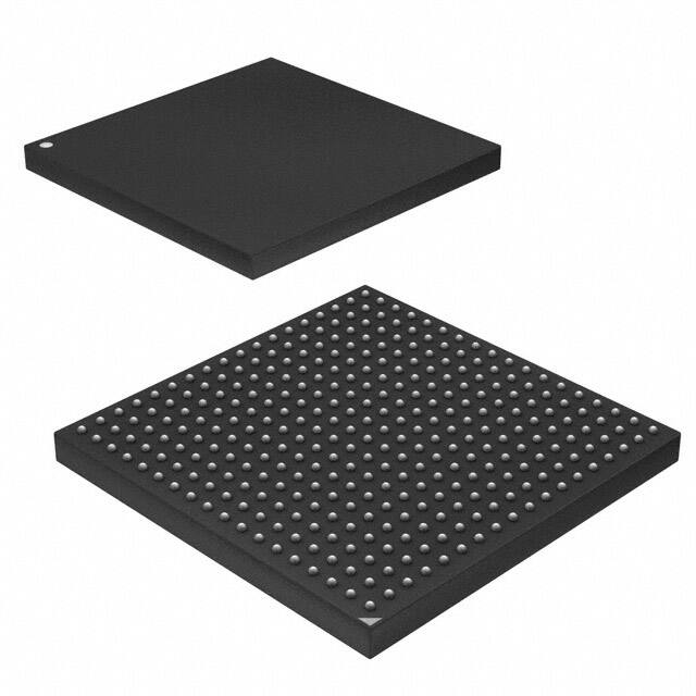
– 324-ball TFBGA, pitch 0.8 mm
AT91 ARM
Thumb-based
Microcontrollers
AT91SAM9G45
Preliminary
6438E–ATARM–16-Dec-09
�1. Description
The ARM926EJ-S based AT91SAM9G45 features the frequently demanded combination of user
interface functionality and high data rate connectivity, including LCD Controller, resistive touchscreen, camera interface, audio, Ethernet 10/100 and high speed USB and SDIO. With the processor running at 400MHz and multiple 100+ Mbps data rate peripherals, the AT91SAM9G45
has the performance and bandwidth to the network or local storage media to provide an adequate user experience.
The AT91SAM9G45 supports the latest generation of DDR2 and NAND Flash memory interfaces for program and data storage. An internal 133 MHz multi-layer bus architecture associated
with 37 DMA channels, a dual external bus interface and distributed memory including a 64KByte SRAM which can be configured as a tightly coupled memory (TCM) sustains the high
bandwidth required by the processor and the high speed peripherals.
The I/Os support 1.8V or 3.3V operation, which are independently configurable for the memory
interface and peripheral I/Os. This feature completely eliminates the need for any external level
shifters. In addition it supports 0.8 ball pitch package for low cost PCB manufacturing.
The AT91SAM9G45 power management controller features efficient clock gating and a battery
backup section minimizing power consumption in active and standby modes.
2
AT91SAM9G45
6438E–ATARM–16-Dec-09
�6438E–ATARM–16-Dec-09
PDC
DBGU
AIC
MCI0/MCI1
SD/SDIO
CE ATA
TWI0
TWI1
PIOE
FIFO
PIOD
RSTC
PIOA
POR
RTC
PIOB
PIOC
POR
VDDCORE
SHDC
RTT
4
GPBR
RC
OSC 32K
PIT
WDT
OSC12M
PLLUTMI PMC
PLLA
VDDBU
NRST
XIN32
XOUT32
SHDN
WKUP
XIN
XOUT
DRXD
DTXD
FIQ
IRQ
System Controller
PIO
JTA
GS
EL
NT
RS
T
TD
I
TD
O
TM
TC S
K
RT
CK
USART0
USART1
USART2
USART3
PDC
ROM
64KB
SRAM
64KB
4-CH
PWM
I
TC0
TC1
TC2
D
DCache
ICache
MMU 32 Kbytes
32 Kbytes
ITCM DTCM Bus Interface
ARM926EJ-S
In-Circuit Emulator
JTAG / Boundary Scan
S
PB
TC3
TC4
TC5
DMA
DMA
HS
USB
HS
Transceiver
DMA
LCD
PIO
TRNG
SPI0
SPI1
PDC
PIO
SSC0
SSC1
PDC
Peripheral
DMA
Controller
DMA
ISI
SSC0_, SSC1_
Peripheral
Bridge
Multi-Layer AHB Matrix
HS EHCI
USB HOST
PA
HS
Transceiver
AC97
PDC
DMA
EMAC
PDC
8-CH
10Bit ADC
TouchScreen
8-CH
DMA
HF
S
HH DP
SD A,H
P F
A
,H SDM
HS A
VB
DM
G
A
DF
S
DH DP/
SD HFS
P/H DP
HS B,
LC
D
D
PB FSD
D
LC D0
,D M
HS /H
D -L
D F
L VS CD
S
M
C
D YN D2
/H DM
HS B
L DO C 3
D
DM
D T ,LC
LC EN CK DH
B
SY
DP ,LC
NC
IS WR DC
I_
, C
I DO LC
S
I_ -IS DM
IS PCK I_D OD
I_
11
IS HS
I
_ Y
IS VS NC
I_M YN
C
C
K
ET
X
ET CK
X
E
EC EN RX
-E C
R
ER S-E TX K
E
ERXER COL R
X ET 0-E ERX
X R D
EM 0-ET X3 V
EMDC X3
DI
O
BM
APB
SPI0_, SPI1_
M
CI
M 0_D
CI
0_ A0C M
M DA CI0
C
,M _
M I0_ CI DA
CI
C
1_ 7
1
_D K,M CD
A0 CI A
-M 1_C
C
I
1_ K
DA
TW
7
TW D0
CK -TW
0D
CT TW 1
S C
RT 0- K1
S CT
SC 0-R S3
K T
RD 0-S S3
X C
TX 0-R K3
D
D
0- X3
TX
PW
D3
M
0PW
TC
M
LK
3
T 0
I
O -TC
A0 L
-T K2
TI
IO
O
TC B0 A2
-T
L
TI K3 IO
O - B
TI A3 TCL 2
O B3 TIOK5
-T A5
IO
B
NP 5
NPCS
C 3
NP S2
NPCS
1
C
SP S0
C
M K
O
M SI
T ISO
K
0
TF -TK
TD 0-T 1
F
R 0-T 1
D
0 D
R -RD1
F
0
RK -R 1
0- F1
AC RK1
AC97C
9 K
AC 7F
S
AC97R
X
TS 97T
AD X
TR
A IG
D
0X
AD P
1
AD XM
2Y
GP
AD AD3 P
Y
4
TS -GP M
A
DVAD7
VD RE
DA F
GN NA
DA
N
Static
Memory
Controller
CF
NAND Flash
Controller
ECC
DDR2/
LPDDR/
SDRAM
Controller
EBI
DDR2
LPDDR
D16-D31
NWAIT
DQM[2..3]
A19-A24
NCS4/CFCS0
NCS5/CFCS1
A25/CFRNW
CFCE1-CFCE2
NCS2
NCS3/NANDCS
D0-D15
A0/NBS0
A1/NBS2/NWR2
A2-A15, A18
A16/BA0
A17/BA1
NCS1/SDCS
SDCK, #SDCK, SDCKE
RAS, CAS
SDWE, SDA10
DQM[0..1]
DQS[0..1]
NRD
NWR0/NWE
NWR1/NBS1
NWR3/NBS3
NCS0
NANDOE, NANDWE
DDR_CS
DDR_CLK,#DDR_CLK
DDR_CKE
DDR_RAS, DDR_CAS
DDR_WE
DDR_BA0, DDR_BA1
DDR_A0-DDR_A13
DDR_D0-DDR_D15
DDR_VREF
DDR_DQM[0..1]
DDR_DQS[0..1]
Figure 2-1.
PCK0-PCK1
TST
AT91SAM9G45
2. Block Diagram
AT91SAM9G45 Block Diagram
3
�3. Signal Description
Table 3-1 gives details on the signal names classified by peripheral.
Table 3-1.
Signal Name
Signal Description List
Function
Type
Active
Level
Reference
Voltage
Comments
Power Supplies
VDDIOM0
DDR2 I/O Lines Power Supply
Power
1.65V to 1.95V
VDDIOM1
EBI I/O Lines Power Supply
Power
1.65V to 1.95V or 3.0V to3.6V
VDDIOP0
Peripherals I/O Lines Power Supply
Power
1.65V to 3.6V
VDDIOP1
Peripherals I/O Lines Power Supply
Power
1.65V to 3.6V
VDDIOP2
ISI I/O Lines Power Supply
Power
1.65V to 3.6V
VDDBU
Backup I/O Lines Power Supply
Power
1.8V to 3.6V
VDDANA
Analog Power Supply
Power
3.0V to 3.6V
VDDPLLA
PLLA Power Supply
Power
0.9V to 1.1V
VDDPLLUTMI
PLLUTMI Power Supply
Power
0.9V to 1.1V
VDDOSC
Oscillator Power Supply
Power
1.65V to 3.6V
VDDCORE
Core Chip Power Supply
Power
0.9V to 1.1V
VDDUTMIC
UDPHS and UHPHS UTMI+ Core
Power Supply
Power
0.9V to 1.1V
VDDUTMII
UDPHS and UHPHS UTMI+ interface
Power Supply
Power
3.0V to 3.6V
GNDIOM
DDR2 and EBI I/O Lines Ground
Ground
GNDIOP
Peripherals and ISI I/O lines Ground
Ground
GNDCORE
Core Chip Ground
Ground
GNDOSC
PLLA, PLLUTMI and Oscillator
Ground
Ground
GNDBU
Backup Ground
Ground
GNDUTMI
UDPHS and UHPHS UTMI+ Core and
interface Ground
Ground
GNDANA
Analog Ground
Ground
Clocks, Oscillators and PLLs
XIN
Main Oscillator Input
Input
XOUT
Main Oscillator Output
Output
XIN32
Slow Clock Oscillator Input
Input
XOUT32
Slow Clock Oscillator Output
Output
VBG
Bias Voltage Reference for USB
Analog
PCK0 - PCK1
Programmable Clock Output
Output
4
(1)
AT91SAM9G45
6438E–ATARM–16-Dec-09
�AT91SAM9G45
Table 3-1.
Signal Description List (Continued)
Signal Name
Function
Type
Active
Level
Reference
Voltage
Comments
Shutdown, Wakeup Logic
SHDN
Shut-Down Control
Output
VDDBU
Driven at 0V only.
0: The device is in backup
mode
1: The device is running (not in
backup mode).
WKUP
Wake-Up Input
Input
VDDBU
Accept between 0V and
VDDBU.
ICE and JTAG
TCK
Test Clock
Input
VDDIOP0
No pull-up resistor, Schmitt
trigger
TDI
Test Data In
Input
VDDIOP0
No pull-up resistor, Schmitt
trigger
TDO
Test Data Out
Output
VDDIOP0
TMS
Test Mode Select
Input
VDDIOP0
No pull-up resistor, Schmitt
trigger
JTAGSEL
JTAG Selection
Input
VDDBU
Pull-down resistor (15 kΩ).
RTCK
Return Test Clock
Output
VDDIOP0
Reset/Test
VDDIOP0
Pull-Up resistor (100 kΩ),
Schmitt trigger
Input
VDDBU
Pull-down resistor (15 kΩ),
Schmitt trigger
Test Reset Signal
Input
VDDIOP0
Pull-Up resistor (100 kΩ),
Schmitt trigger
Boot Mode Select
Input
VDDIOP0
must be connected to GND or
VDDIOP0.
NRST
Microcontroller Reset (2)
I/O
TST
Test Mode Select
NTRST
BMS
Low
Debug Unit - DBGU
DRXD
Debug Receive Data
Input
(1)
DTXD
Debug Transmit Data
Output
(1)
Advanced Interrupt Controller - AIC
IRQ
External Interrupt Input
Input
(1)
FIQ
Fast Interrupt Input
Input
(1)
PIO Controller - PIOA- PIOB - PIOC - PIOD - PIOE
PA0 - PA31
Parallel IO Controller A
I/O
(1)
PB0 - PB31
Parallel IO Controller B
I/O
(1)
PC0 - PC31
Parallel IO Controller C
I/O
(1)
Pulled-up input at reset
(100kΩ)(3), Schmitt trigger
Pulled-up input at reset
(100kΩ)(3), Schmitt trigger
Pulled-up input at reset
(100kΩ)(3), Schmitt trigger
5
6438E–ATARM–16-Dec-09
�Table 3-1.
Signal Description List (Continued)
Signal Name
Function
Type
Active
Level
Reference
Voltage
PD0 - PD31
Parallel IO Controller D
I/O
(1)
PE0 - PE31
Parallel IO Controller E
I/O
(1)
Comments
Pulled-up input at reset
(100kΩ)(3), Schmitt trigger
Pulled-up input at reset
(100kΩ)(3), Schmitt trigger
DDR Memory Interface- DDR2/SDRAM/LPDDR Controller
DDR_D0 DDR_D15
Data Bus
I/O
VDDIOM0
Pulled-up input at reset
DDR_A0 DDR_A13
Address Bus
Output
VDDIOM0
0 at reset
DDR_CLK#DDR_CLK
DDR differential clock input
Output
VDDIOM0
DDR_CKE
DDR Clock Enable
Output
High
VDDIOM0
DDR_CS
DDR Chip Select
Output
Low
VDDIOM0
DDR_WE
DDR Write Enable
Output
Low
VDDIOM0
DDR_RASDDR_CAS
Row and Column Signal
Output
Low
VDDIOM0
DDR_DQM[0..1]
Write Data Mask
Output
VDDIOM0
DDR_DQS[0..1]
Data Strobe
Output
VDDIOM0
DDR_BA0 DDR_BA1
Bank Select
Output
VDDIOM0
DDR_VREF
Reference Voltage
Input
VDDIOM0
External Bus Interface - EBI
D0 -D31
Data Bus
I/O
VDDIOM1
Pulled-up input at reset
A0 - A25
Address Bus
Output
VDDIOM1
0 at reset
NWAIT
External Wait Signal
Input
Low
VDDIOM1
Static Memory Controller - SMC
NCS0 - NCS5
Chip Select Lines
Output
Low
VDDIOM1
NWR0 - NWR3
Write Signal
Output
Low
VDDIOM1
NRD
Read Signal
Output
Low
VDDIOM1
NWE
Write Enable
Output
Low
VDDIOM1
NBS0 - NBS3
Byte Mask Signal
Output
Low
VDDIOM1
CompactFlash Support
CFCE1 - CFCE2
CompactFlash Chip Enable
Output
Low
VDDIOM1
CFOE
CompactFlash Output Enable
Output
Low
VDDIOM1
CFWE
CompactFlash Write Enable
Output
Low
VDDIOM1
CFIOR
CompactFlash IO Read
Output
Low
VDDIOM1
CFIOW
CompactFlash IO Write
Output
Low
VDDIOM1
CFRNW
CompactFlash Read Not Write
Output
6
VDDIOM1
AT91SAM9G45
6438E–ATARM–16-Dec-09
�AT91SAM9G45
Table 3-1.
Signal Description List (Continued)
Signal Name
CFCS0 -CFCS1
Function
Type
CompactFlash Chip Select Lines
Output
Active
Level
Low
Reference
Voltage
Comments
VDDIOM1
NAND Flash Support
NANDCS
NAND Flash Chip Select
Output
Low
VDDIOM1
NANDOE
NAND Flash Output Enable
Output
Low
VDDIOM1
NANDWE
NAND Flash Write Enable
Output
Low
VDDIOM1
DDR2/SDRAM/LPDDR Controller
SDCK,#SDCK
DDR2/SDRAM differential clock
Output
VDDIOM1
SDCKE
DDR2/SDRAM Clock Enable
Output
High
VDDIOM1
SDCS
DDR2/SDRAM Controller Chip Select
Output
Low
VDDIOM1
BA0 - BA1
Bank Select
Output
SDWE
DDR2/SDRAM Write Enable
Output
Low
VDDIOM1
RAS - CAS
Row and Column Signal
Output
Low
VDDIOM1
SDA10
SDRAM Address 10 Line
Output
VDDIOM1
DQS[0..1]
Data Strobe
Output
VDDIOM1
DQM[0..3]
Write Data Mask
Output
VDDIOM1
VDDIOM1
High Speed Multimedia Card Interface - HSMCIx
MCIx_CK
Multimedia Card Clock
I/O
(1)
MCIx_CDA
Multimedia Card Slot A Command
I/O
(1)
MCIx_DA0 MCIx_DA7
Multimedia Card Slot A Data
I/O
(1)
Universal Synchronous Asynchronous Receiver Transmitter - USARTx
SCKx
USARTx Serial Clock
I/O
(1)
TXDx
USARTx Transmit Data
Output
(1)
RXDx
USARTx Receive Data
Input
(1)
RTSx
USARTx Request To Send
Output
(1)
CTSx
USARTx Clear To Send
Input
(1)
Synchronous Serial Controller - SSCx
TDx
SSC Transmit Data
Output
(1)
RDx
SSC Receive Data
Input
(1)
TKx
SSC Transmit Clock
I/O
(1)
RKx
SSC Receive Clock
I/O
(1)
TFx
SSC Transmit Frame Sync
I/O
(1)
RFx
SSC Receive Frame Sync
I/O
(1)
7
6438E–ATARM–16-Dec-09
�Table 3-1.
Signal Name
Signal Description List (Continued)
Function
Type
Active
Level
Reference
Voltage
Comments
AC97 Controller - AC97C
AC97RX
AC97 Receive Signal
Input
(1)
AC97TX
AC97 Transmit Signal
Output
(1)
AC97FS
AC97 Frame Synchronization Signal
Output
(1)
AC97CK
AC97 Clock signal
Input
(1)
Time Counter - TCx
TCLKx
TC Channel x External Clock Input
Input
(1)
TIOAx
TC Channel x I/O Line A
I/O
(1)
TIOBx
TC Channel x I/O Line B
I/O
(1)
Pulse Width Modulation Controller - PWM
PWMx
Pulse Width Modulation Output
(1)
Output
Serial Peripheral Interface - SPIx_
SPIx_MISO
Master In Slave Out
I/O
(1)
SPIx_MOSI
Master Out Slave In
I/O
(1)
SPIx_SPCK
SPI Serial Clock
I/O
(1)
SPIx_NPCS0
SPI Peripheral Chip Select 0
I/O
Low
(1)
SPIx_NPCS1SPIx_NPCS3
SPI Peripheral Chip Select
Output
Low
(1)
Two-Wire Interface
TWDx
Two-wire Serial Data
I/O
(1)
TWCKx
Two-wire Serial Clock
I/O
(1)
USB Host High Speed Port - UHPHS
HFSDPA
USB Host Port A Full Speed Data +
Analog
VDDUTMII
HFSDMA
USB Host Port A Full Speed Data -
Analog
VDDUTMII
HHSDPA
USB Host Port A High Speed Data +
Analog
VDDUTMII
HHSDMA
USB Host Port A High Speed Data -
Analog
VDDUTMII
HFSDPB
USB Host Port B Full Speed Data +
Analog
VDDUTMII
Multiplexed with DFSDP
HFSDMB
USB Host Port B Full Speed Data -
Analog
VDDUTMII
Multiplexed with DFSDM
HHSDPB
USB Host Port B High Speed Data +
Analog
VDDUTMII
Multiplexed with DHSDP
HHSDMB
USB Host Port B High Speed Data -
Analog
VDDUTMII
Multiplexed with DHSDM
USB Device High Speed Port - UDPHS
DFSDM
USB Device Full Speed Data -
Analog
VDDUTMII
DFSDP
USB Device Full Speed Data +
Analog
VDDUTMII
DHSDM
USB Device High Speed Data -
Analog
VDDUTMII
DHSDP
USB Device High Speed Data +
Analog
VDDUTMII
8
AT91SAM9G45
6438E–ATARM–16-Dec-09
�AT91SAM9G45
Table 3-1.
Signal Description List (Continued)
Signal Name
Function
Type
Active
Level
Reference
Voltage
Comments
Ethernet 10/100
ETXCK
ERXCK
Transmit Clock or Reference Clock
Receive Clock
Input
(1)
MII only, REFCK in RMII
Input
(1)
MII only
ETXEN
Transmit Enable
Output
(1)
ETX0-ETX3
Transmit Data
Output
(1)
ETX0-ETX1 only in RMII
Output
(1)
MII only
Input
(1)
RXDV in MII, CRSDV in RMII
ERX0-ERX1 only in RMII
ETXER
ERXDV
Transmit Coding Error
Receive Data Valid
ERX0-ERX3
Receive Data
Input
(1)
ERXER
Receive Error
Input
(1)
ECRS
Carrier Sense and Data Valid
Input
(1)
MII only
Input
(1)
MII only
ECOL
Collision Detect
EMDC
Management Data Clock
Output
(1)
EMDIO
Management Data Input/Output
I/O
(1)
Image Sensor Interface
ISI_D0-ISI_D11
Image Sensor Data
Input
VDDIOP2
ISI_MCK
Image sensor Reference clock
output
VDDIOP2
ISI_HSYNC
Image Sensor Horizontal Synchro
input
VDDIOP2
ISI_VSYNC
Image Sensor Vertical Synchro
input
VDDIOP2
ISI_PCK
Image Sensor Data clock
input
VDDIOP2
LCD Controller - LCDC
LCDD0 LCDD23
LCD Data Bus
Output
VDDIOP1
LCDVSYNC
LCD Vertical Synchronization
Output
VDDIOP1
LCDHSYNC
LCD Horizontal Synchronization
Output
VDDIOP1
LCDDOTCK
LCD Dot Clock
Output
VDDIOP1
LCDDEN
LCD Data Enable
Output
VDDIOP1
LCDCC
LCD Contrast Control
Output
VDDIOP1
LCDPWR
LCD panel Power enable control
Output
VDDIOP1
LCDMOD
LCD Modulation signal
Output
VDDIOP1
Touch Screen Analog-to-Digital Converter
AD0XP
Analog input channel 0 or
Touch Screen Top channel
Analog
VDDANA
Multiplexed with AD0
AD1XM
Analog input channel 1 or
Touch Screen Bottom channel
Analog
VDDANA
Multiplexed with AD1
AD2YP
Analog input channel 2 or
Touch Screen Right channel
Analog
VDDANA
Multiplexed with AD2
9
6438E–ATARM–16-Dec-09
�Table 3-1.
Signal Description List (Continued)
Signal Name
Function
Type
Active
Level
Reference
Voltage
Comments
Multiplexed with AD3
AD3YM
Analog input channel 3 or
Touch Screen Left channel
Analog
VDDANA
GPAD4-GPAD7
Analog Inputs
Analog
VDDANA
TSADTRG
ADC Trigger
Input
VDDANA
TSADVREF
ADC Reference
Analog
VDDANA
Notes:
1. Refer to peripheral multiplexing tables in Section 8.4 “Peripheral Signals Multiplexing on I/O Lines” for these signals.
2. When configured as an input, the NRST pin enables asynchronous reset of the device when asserted low. This allows connection of a simple push button on the NRST pin as a system-user reset.
3. Programming of this pull-up resistor is performed independently for each I/O line through the PIO Controllers. After reset, all
the I/O lines default as inputs with pull-up resistors enabled, except those which are multiplexed with the External Bus Interface signals that require to be enabled as Peripheral at reset. This is explicitly indicated in the column “Reset State” of the
peripheral multiplexing tables.
10
AT91SAM9G45
6438E–ATARM–16-Dec-09
�AT91SAM9G45
4. Package and Pinout
The AT91SAM9G45 is delivered in a 324-ball TFBGA package.
4.1
Mechanical Overview of the 324-ball TFBGA Package
Figure 4-1 shows the orientation of the 324-ball TFBGA Package
Figure 4-1.
Orientation of the 324-ball TFBGA Package
Bottom VIEW
V
U
T
R
P
N
M
L
K
J
H
G
F
E
D
C
B
A
1 2
3 4 5 6 7 8 9 10 11 12 13 14 15
16 17 18
11
6438E–ATARM–16-Dec-09
�4.2
324-ball TFBGA Package Pinout
Table 4-1.
AT91SAM9G45 Pinout for 324-ball BGA Package
Pin
Signal Name
Pin
Signal Name
Pin
Signal Name
Pin
A1
PC27
E10
NANDWE
K1
PE21
P10
Signal Name
TMS
A2
PC28
E11
DQS1
K2
PE23
P11
VDDPLLA
A3
PC25
E12
D13
K3
PE26
P12
PB20
A4
PC20
E13
D11
K4
PE22
P13
PB31
A5
PC12
E14
A4
K5
PE24
P14
DDR_D7
A6
PC7
E15
A8
K6
PE25
P15
DDR_D3
A7
PC5
E16
A9
K7
PE27
P16
DDR_D4
A8
PC0
E17
A7
K8
PE28
P17
DDR_D5
A9
NWR3/NBS3
E18
VDDCORE
K9
VDDIOP0
P18
DDR_D10
A10
NCS0
F1
PD22
K10
VDDIOP0
R1
PA18
A11
DQS0
F2
PD24
K11
GNDIOM
R2
PA20
A12
RAS
F3
SHDN
K12
GNDIOM
R3
PA24
A13
SDCK
F4
PE1
K13
VDDIOM0
R4
PA30
PB4
A14
NSDCK
F5
PE3
K14
DDR_A7
R5
A15
D7
F6
VDDIOM1
K15
DDR_A8
R6
PB13
A16
DDR_VREF
F7
PC19
K16
DDR_A9
R7
PD0
A17
D0
F8
PC14
K17
DDR_A11
R8
PD9
A18
A14
F9
PC4
K18
DDR_A10
R9
PD18
B1
PC31
F10
NCS1/SDCS
L1
PA0
R10
TDI
B2
PC29
F11
NRD
L2
PE30
R11
RTCK
B3
PC30
F12
SDWE
L3
PE29
R12
PB22
B4
PC22
F13
A0/NBS0
L4
PE31
R13
PB29
B5
PC17
F14
A1/NBS2/NWR2
L5
PA2
R14
DDR_D6
B6
PC10
F15
A3
L6
PA4
R15
DDR_D1
B7
PC11
F16
A6
L7
PA8
R16
DDR_D0
B8
PC2
F17
A5
L8
PD2
R17
HHSDMA
B9
SDA10
F18
A2
L9
PD13
R18
HFSDMA
B10
A17/BA1
G1
PD25
L10
PD29
T1
PA22
B11
DQM0
G2
PD23
L11
PD31
T2
PA25
B12
SDCKE
G3
PE6
L12
VDDIOM0
T3
PA26
B13
D12
G4
PE0
L13
VDDIOM0
T4
PB0
B14
D8
G5
PE2
L14
DDR_A1
T5
PB6
B15
D4
G6
PE8
L15
DDR_A3
T6
PB16
B16
D3
G7
PE4
L16
DDR_A4
T7
PD1
B17
A15
G8
PE11
L17
DDR_A6
T8
PD11
B18
A13
G9
GNDCORE
L18
DDR_A5
T9
PD19
C1
XIN32
G10
VDDIOM1
M1
PA1
T10
PD30
C2
GNDANA
G11
VDDIOM1
M2
PA5
T11
BMS
C3
WKUP
G12
VDDCORE
M3
PA6
T12
PB8
C4
PC26
G13
VDDCORE
M4
PA7
T13
PB30
C5
PC21
G14
DDR_DQM0
M5
PA10
T14
DDR_D2
C6
PC15
G15
DDR_DQS1
M6
PA14
T15
PB21
C7
PC9
G16
DDR_BA1
M7
PB14
T16
PB23
C8
PC3
G17
DDR_BA0
M8
PD4
T17
HHSDPA
C9
NWR0/NWE
G18
DDR_DQS0
M9
PD15
T18
HFSDPA
C10
A16/BA0
H1
PD26
M10
NRST
U1
PA27
C11
CAS
H2
PD27
M11
PB11
U2
PA29
C12
D15
H3
VDDIOP1
M12
PB25
U3
PA28
12
AT91SAM9G45
6438E–ATARM–16-Dec-09
�AT91SAM9G45
Table 4-1.
AT91SAM9G45 Pinout for 324-ball BGA Package (Continued)
Pin
Signal Name
Pin
Signal Name
Pin
Signal Name
Pin
C13
D10
H4
PE13
M13
PB27
U4
Signal Name
PB3
C14
D6
H5
PE5
M14
VDDIOM0
U5
PB7
C15
D2
H6
PE7
M15
DDR_D14
U6
PB17
C16
GNDIOM
H7
PE9
M16
DDR_D15
U7
PD7
C17
A18
H8
PE10
M17
DDR_A0
U8
PD10
C18
A12
H9
GNDCORE
M18
DDR_A2
U9
PD14
D1
XOUT32
H10
GNDIOP
N1
PA3
U10
TCK
D2
PD20
H11
VDDCORE
N2
PA9
U11
VDDOSC
D3
GNDBU
H12
GNDIOM
N3
PA12
U12
GNDOSC
D4
VDDBU
H13
GNDIOM
N4
PA15
U13
PB10
D5
PC24
H14
DDR_CS
N5
PA16
U14
PB26
D6
PC18
H15
DDR_WE
N6
PA17
U15
HHSDPB/DHSDP
D7
PC13
H16
DDR_DQM1
N7
PB18
U16
HHSDMB/DHSDM
D8
PC6
H17
DDR_CAS
N8
PD6
U17
GNDUTMI
D9
NWR1/NBS1
H18
DDR_NCLK
N9
PD16
U18
VDDUTMIC
D10
NANDOE
J1
PE19
N10
NTRST
V1
PA31
D11
DQM1
J2
PE16
N11
PB9
V2
PB1
D12
D14
J3
PE14
N12
PB24
V3
PB2
D13
D9
J4
PE15
N13
PB28
V4
PB5
D14
D5
J5
PE12
N14
DDR_D13
V5
PB15
D15
D1
J6
PE17
N15
DDR_D8
V6
PD3
D16
VDDIOM1
J7
PE18
N16
DDR_D9
V7
PD5
D17
A11
J8
PE20
N17
DDR_D11
V8
PD12
D18
A10
J9
GNDCORE
N18
DDR_D12
V9
PD17
E1
PD21
J10
GNDCORE
P1
PA11
V10
TDO
E2
TSADVREF
J11
GNDIOP
P2
PA13
V11
XOUT
E3
VDDANA
J12
GNDIOM
P3
PA19
V12
XIN
E4
JTAGSEL
J13
GNDIOM
P4
PA21
V13
VDDPLLUTMI
E5
TST
J14
DDR_A12
P5
PA23
V14
VDDIOP2
E6
PC23
J15
DDR_A13
P6
PB12
V15
HFSDPB/DFSDP
E7
PC16
J16
DDR_CKE
P7
PB19
V16
HFSDMB/DFSDM
E8
PC8
J17
DDR_RAS
P8
PD8
V17
VDDUTMII
E9
PC1
J18
DDR_CLK
P9
PD28
V18
VBG
13
6438E–ATARM–16-Dec-09
�5. Power Considerations
5.1
Power Supplies
The AT91SAM9G45 has several types of power supply pins:
• VDDCORE pins: Power the core, including the processor, the embedded memories and the
peripherals; voltage ranges from 0.9V to 1.1V, 1.0V nominal.
• VDDIOM0 pins: Power the DDR2/LPDDR I/O lines; voltage ranges between 1.65V and 1.95V
(1.8V typical).
• VDDIOM1 pins: Power the External Bus Interface 1 I/O lines; voltage ranges between 1.65V
and 1.95V (1.8V typical) or between 3.0V and 3.6V (3.3V nominal).
• VDDIOP0, VDDIOP1, VDDIOP2 pins: Power the Peripherals I/O lines; voltage ranges from
1.65V to 3.6V.
• VDDBU pin: Powers the Slow Clock oscillator, the internal RC oscillator and a part of the
System Controller; voltage ranges from 1.8V to 3.6V.
• VDDPLLUTMI Powers the PLLUTMI cell; voltage range from 0.9V to 1.1V.
• VDDUTMIC pin: Powers the USB device and host UTMI+ core; voltage range from 0.9V to
1.1V, 1.0V nominal.
• VDDUTMII pin: Powers the USB device and host UTMI+ interface; voltage range from 3.0V to
3.6V, 3.3V nominal.
• VDDPLLA pin: Powers the PLLA cell; voltage ranges from 0.9V to 1.1V.
• VDDOSC pin: Powers the Main Oscillator cells; voltage ranges from 1.65V to 3.6V
• VDDANA pin: Powers the Analog to Digital Converter; voltage ranges from 3.0V to 3.6V, 3.3V
nominal.
Ground pins GND are common to VDDIOM0, VDDIOM1, VDDIOP0, VDDIOP1 and VDDIOP2
power supplies. Separated ground pins are provided for VDDUTMIC, VDDUTMII, VDDBU,
VDDOSC, VDDPLLA, VDDPLLUTMI and VDDANA. These ground pins are respectively
GNDUTMIC, GNDUTMII, GNDBU, GNDOSC, GNDPLLA, GNDPLLUTMI and GNDANA.
14
AT91SAM9G45
6438E–ATARM–16-Dec-09
�AT91SAM9G45
6. Memories
Figure 6-1.
AT91SAM9G45 Memory Mapping
0x00000000
Address Memory Space
Internal Memories
0x00000000
Internal Memories
0xFFFF0000
Reserved
Boot Memory
0xFFFFE200
0x00100000
ECC
ITCM
0x10000000
0xFFFFE400
0x00200000
DDRSDRC1
DTCM
EBI Chip Select 0
0xFFFFE600
0x00300000
DDRSDRC0
SRAM
0x20000000
0xFFFFE800
0x00400000
EBI Chip Select 1
DDR2-LPDDR-SDRAM
0x30000000
SMC
ROM
0xFFFFEA00
0x00500000
MATRIX
LCDC
23
0x00600000
0xFFFFEE00
0x00700000
0x50000000
AIC
UHP EHCI
0xFFFFF200
0x00900000
PIOA
Reserved
0xFFFFF400
0x00A00000
EBI Chip Select 4
Compact Flash Slot 0
0x60000000
0x70000000
Undefined (Abort)
Internal Peripherals
+0x40
+0x80
TC0
TC0
TC0
TC1
TC0
0xFFF88000
TWI1
0xFFFFFFFF
27
0xFFF8C000
+18
+18
11
12
13
0xFFF90000
USART1
block peripheral
ID
(+ : wired-or)
0xFFF94000
USART2
0xFFF9C000
SSC0
0xFFFA0000
SSC1
0xFFFA4000
SPI0
0xFFFA8000
SPI1
0xFFFAC000
AC97C
0xFFFB0000
TSADCC
0xFFFB4000
ISI
0xFFFB8000
PWM
0xFFFBC000
EMAC
0xFFFC0000
+0x10
+0x30
+0x40
+0x50
7
+0x60
8
+0x70
SYSC
RSTC
SYSC
SHDWC
SYSC
RTT
SYSC
PIT
SYSC
WDT
SYSC
SCKCR
SYSC
GPBR
SYSC
9
0xFFFFFDB0
10
0xFFFFFDC0
0xFFF98000
USART3
0xFFFFFD00
+0x20
USART0
offset
0xFFFFFC00
0;31
2
3
4
+5
+5
PMC
0xFFF80000
TWI0
Internal Peripherals
PIOE
TC2
0xFFF84000
0xFFFFF800
0xFFFFFA00
0xFFF78000
UDPHS
PIOC
PIOD
Reserved
HSMCI0
0xF0000000
0xFFFFF600
0x0FFFFFFF
0xFFF7C000
DDR2-LPDDR
Chip Select
PIOB
Undefined (Abort)
0xF0000000
EBI Chip Select 5
Compact Flash Slot 1
0x80000000
0xFFFFF000
0x00800000
EBI Chip Select 3
NANDFlash
21
DBGU
UHP OHCI
0x40000000
0xFFFFEC00
DMAC
UDPHS (DMA)
EBI Chip Select 2
System Controller
1
1
1
1
1
1
1
Reserved
RTC
Reserved
16
0xFFFFFFFF
17
14
15
24
20
26
19
25
Reserved
0xFFFC4000
Reserved
0xFFFC8000
Reserved
0xFFFCC000
TRNG
6
0xFFFD0000
HSMCI1
0xFFFD4000
+0x40
+0x80
TC1
TC3
TC1
TC4
TC1
TC5
29
0xFFFD8000
Reserved
0xFFFFC000
System controller
0xFFFFFFFF
15
6438E–ATARM–16-Dec-09
�6.1
Memory Mapping
A first level of address decoding is performed by the AHB Bus Matrix, i.e., the implementation of
the Advanced High performance Bus (AHB) for its Master and Slave interfaces with additional
features.
Decoding breaks up the 4 Gbytes of address space into 16 banks of 256 Mbytes. The banks 1 to
6 are directed to the EBI that associates these banks to the external chip selects NCS0 to
NCS5.
The bank 7 is directed to the DDRSDRC0 that associates this bank to DDR_NCS chip select
and so dedicated to the 4-port DDR2/ LPDDR controller.
The bank 0 is reserved for the addressing of the internal memories, and a second level of
decoding provides 1 Mbyte of internal memory area. The bank 15 is reserved for the peripherals
and provides access to the Advanced Peripheral Bus (APB).
Other areas are unused and performing an access within them provides an abort to the master
requesting such an access.
6.2
6.2.1
Embedded Memories
Internal SRAM
The AT91SAM9G45 product embeds a total of 64 Kbytes high-speed SRAM split in 4 blocks of
16 KBytes connected to one slave of the matrix. After reset and until the Remap Command is
performed, the four SRAM blocks are contiguous and only accessible at address 0x00300000.
After Remap, the SRAM also becomes available at address 0x0.
Figure 6-2.
Internal SRAM Reset
RAM
RAM
Remap
64K
0x00300000
64K
0x00000000
The AT91SAM9G45 device embeds two memory features. The processor Tightly Coupled Memory Interface (TCM) that allows the processor to access the memory up to processor speed
(PCK) and the interface on the AHB side allowing masters to access the memory at AHB speed
(MCK).
A wait state is necessary to access the TCM at 400 MHz. Setting the bit NWS_TCM in the bus
Matrix TCM Configuration Register of the matrix inserts a wait state on the ITCM and DTCM
accesses.
16
AT91SAM9G45
6438E–ATARM–16-Dec-09
�AT91SAM9G45
6.2.2
TCM Interface
On the processor side, this Internal SRAM can be allocated to two areas.
• Internal SRAM A is the ARM926EJ-S Instruction TCM. The user can map this SRAM block
anywhere in the ARM926 instruction memory space using CP15 instructions and the TCR
configuration register located in the Chip Configuration User Interface. This SRAM block is
also accessible by the ARM926 Masters and by the AHB Masters through the AHB bus
• Internal SRAM B is the ARM926EJ-S Data TCM. The user can map this SRAM block
anywhere in the ARM926 data memory space using CP15 instructions. This SRAM block is
also accessible by the ARM926 Data Master and by the AHB Masters through the AHB bus.
• Internal SRAM C is only accessible by all the AHB Masters. After reset and until the Remap
Command is performed, this SRAM block is accessible through the AHB bus at address
0x0030 0000 by all the AHB Masters. After Remap, this SRAM block also becomes
accessible through the AHB bus at address 0x0 by the ARM926 Instruction and the ARM926
Data Masters.
Within the 64 Kbyte SRAM size available, the amount of memory assigned to each block is software programmable according to Table 6-1.
Table 6-1.
ITCM and DTCM Memory Configuration
SRAM A ITCM size (KBytes)
seen at 0x100000 through AHB
SRAM B DTCM size (KBytes)
seen at 0x200000 through AHB
SRAM C (KBytes)
seen at 0x300000 through AHB
0
0
64
0
64
0
32
32
0
6.2.3
Internal ROM
The AT91SAM9G45 embeds an Internal ROM, which contains the boot ROM and SAM-BA®
program.
At any time, the ROM is mapped at address 0x0040 0000. It is also accessible at address 0x0
(BMS =1) after the reset and before the Remap Command.
6.3
6.3.1
I/O Drive Selection and Delay Control
I/O Drive Selection
The aim of this control is to adapt the signal drive to the frequency. Two bits allow the user to
select High or Low drive for memories data/address/ctrl signals.
• Setting the bit [17], EBI_DRIVE, in the EBI_CSA register of the matrix allows to control the
drive of the EBI.
• Setting the bit [18], DDR_DRIVE, in the EBI_CSA register of the matrix allows to control the
drive of the DDR.
6.3.2
Delay Control
To avoid the simultaneous switching of all the I/Os, a delay can be inserted on the different EBI,
DDR2 and PIO lines.
17
6438E–ATARM–16-Dec-09
�The control of these delays is the following:
• DDR2SDRC
DDR_D[15:0] controlled by 2 registers, DELAY1 and DELAY2, located in the DDR2SDRC user
interface
– DDR_D[0] DELAY1[3:0],
– DDR_D[1] DELAY1[7:4],...
– DDR_D[6] DELAY1[27:24],
– DDR_D[7] DELAY1[31:28]
– DDR_D[8] DELAY2[3:0],
– DDR_D[9] DELAY2[7:4],...,
– DDR_D[14] DELAY2[27:24],
– DDR_D[15] DELAY2[31:28]
DDR_A[13:0] controlled by 2 registers, DELAY3 and DELAY4, located in the DDR2SDRC user
interface
– DDR_A[0] DELAY3[3:0],
– DDR_A[1] DELAY3[7:4], ...,
– DDR_A[6] DELAY3[27:24],
– DDR_A[7] DELAY3[31:28]
– DDR_A[8] DELAY4[3:0],
– DDR_A[9] DELAY4[7:4], ...,
– DDR_A[12] DELAY4[19:16],
– DDR_A[13] DELAY4[23:20]
• EBI (DDR2SDRC\HSMC3\Nandflash)
D[15:0] controlled by 2 registers, DELAY1 and DELAY2, located in the HSMC3 user interface
– D[0] DELAY1[3:0],
– D[1] DELAY1[7:4],...,
– D[6] DELAY1[27:24],
– D[7] DELAY1[31:28]
– D[8] DELAY2[3:0],
– D[9] DELAY2[7:4],...,
– D[14] DELAY2[27:24],
– D[15] DELAY2[31:28]
D[31,16]on PIOC[31:16] controlled by 2 registers, DELAY3 and DELAY4, located in the
HSMC3 user interface
– D[16] DELAY3[3:0],
– D[17] DELAY3[7:4],...,
– D[22] DELAY3[27:24],
– PC[23] DELAY3[31:28]
18
AT91SAM9G45
6438E–ATARM–16-Dec-09
�AT91SAM9G45
– D[24] DELAY4[3:0],
– D[25] DELAY4[7:4],...,
– D[30] DELAY4[27:24],
– D[31] DELAY4[31:28]
A[25:0], controlled by 4 registers, DELAY5, DELAY6, DELAY7and DELAY8, located in the
HSMC3 user interface
– A[0] DELAY5[3:0],
– A[1] DELAY5[7:4],...,
– A[6] DELAY5[27:24],
– A[7] DELAY5[31:28]
– A[8] DELAY6[3:0],
– A[9] DELAY6[7:4],...,
– A[14] DELAY6[27:24],
– A[15] DELAY6[31:28]
– A[16] DELAY7[3:0],
– A[17] DELAY7[7:4],
– A[18] DELAY7[11:8]
A25 on PC[12] and A[24:19] on PC[7:2]
– A19 DELAY7[15:12],
– A20 DELAY7[19:16],...,
– A23 DELAY7[31:28],
– A24 DELAY8[3:0],
– A25 DELAY8[7:4]
• PIOA User interface
The delay can only be inserted on the HSMCI0 and HSMCI1 I/O lines, so on PA[9:2] and
PA[30:23]. The delay is controlled by 2 registers, DELAY1 and DELAY2, located in the PIOA
user interface.
– PA[2] DELAY1[3:0],
– PA[3] DELAY1[7:4],...,
– PA[8] DELAY1[27:24],
– PA[9] DELAY1[31:28]
– PA[23] DELAY2[3:0],
– PA[24] DELAY2[7:4],...,
– PA[29] DELAY2[27:24],
– PA[30] DELAY2[31:28]
7. System Controller
The System Controller is a set of peripherals that allows handling of key elements of the system,
such as power, resets, clocks, time, interrupts, watchdog, etc.
19
6438E–ATARM–16-Dec-09
�The System Controller User Interface also embeds the registers that configure the Matrix and a
set of registers for the chip configuration. The chip configuration registers configure the EBI chip
select assignment and voltage range for external memories.
7.1
System Controller Mapping
The System Controller’s peripherals are all mapped within the highest 16 KBytes of address
space, between addresses 0xFFFF E800 and 0xFFFF FFFF.
However, all the registers of the System Controller are mapped on the top of the address space.
All the registers of the System Controller can be addressed from a single pointer by using the
standard ARM instruction set, as the Load/Store instruction have an indexing mode of ±4 KB.
Figure 7-1 on page 21 shows the System Controller block diagram.
Figure 6-1 on page 15 shows the mapping of the User Interfaces of the System Controller
peripherals.
20
AT91SAM9G45
6438E–ATARM–16-Dec-09
�AT91SAM9G45
7.2
System Controller Block Diagram
Figure 7-1.
AT91SAM9G45 System Controller Block Diagram
System Controller
VDDCORE Powered
irq0-irq2
fiq
periph_irq[2..24]
nirq
nfiq
Advanced
Interrupt
Controller
pit_irq
rtt_irq
wdt_irq
dbgu_irq
pmc_irq
rstc_irq
int
ntrst
por_ntrst
MCK
periph_nreset
Debug
Unit
dbgu_irq
dbgu_txd
dbgu_rxd
MCK
debug
periph_nreset
proc_nreset
PCK
debug
Periodic
Interval
Timer
pit_irq
Watchdog
Timer
wdt_irq
jtag_nreset
SLCK
debug
idle
proc_nreset
ARM926EJ-S
Boundary Scan
TAP Controller
MCK
wdt_fault
WDRPROC
NRST
periph_nreset
Bus Matrix
rstc_irq
por_ntrst
jtag_nreset
VDDCORE
POR
Reset
Controller
periph_nreset
proc_nreset
backup_nreset
VDDBU
VDDBU
POR
VDDBU Powered
SLCK
UPLLCK
UHP48M
SLCK
backup_nreset
Real-Time
Clock
SLCK
backup_nreset
Real-Time
Timer
rtc_irq
rtc_alarm
UHP12M
rtt_irq
periph_nreset
rtt_alarm
periph_irq[25]
USB High Speed
Host Port
SLCK
SHDN
WKUP
backup_nreset
RC
OSC
XIN32
XOUT32
SLOW
CLOCK
OSC
rtt0_alarm
4 General-purpose
Backup Registers
XIN
periph_nreset
USB High Speed
Device Port
periph_irq[24]
SCKCR
SLCK
XOUT
UPLLCK
Shut-Down
Controller
int
12MHz
MAIN OSC
MAINCK
UPLL
UPLLCK
PLLA
PLLACK
Power
Management
Controller
periph_clk[2..30]
pck[0-1]
UHP48M
UHP12M
PCK
MCK
DDR sysclk
pmc_irq
idle
periph_clk[6..30]
periph_nreset
periph_nreset
periph_nreset
periph_clk[2..6]
dbgu_rxd
PA0-PA31
PB0-PB31
PC0-PC31
PD0-PD31
PIO
Controllers
periph_irq[2..6]
irq
fiq
dbgu_txd
Embedded
Peripherals
periph_irq[6..30]
in
out
enable
PE0-PE31
21
6438E–ATARM–16-Dec-09
�7.3
Chip Identification
The AT91SAM9G45 Chip ID is defined in the Debug Unit Chip ID Register and Debug Unit Chip
ID Extension Register.
• Chip ID: 0x819B05A2
• Ext ID: 0x00000004
• JTAG ID: 05B2_703F
• ARM926 TAP ID: 0x0792603F
7.4
Backup Section
The AT91SAM9G45 features a Backup Section that embeds:
• RC Oscillator
• Slow Clock Oscillator
• SCKR register
• RTT
• RTC
• Shutdown Controller
• 4 backup registers
• A part of RSTC
This section is powered by the VDDBU rail.
22
AT91SAM9G45
6438E–ATARM–16-Dec-09
�AT91SAM9G45
8. Peripherals
8.1
Peripheral Mapping
As shown in Figure 6-1, the Peripherals are mapped in the upper 256 Mbytes of the address
space between the addresses 0xFFF7 8000 and 0xFFFC FFFF.
Each User Peripheral is allocated 16K bytes of address space.
8.2
Peripheral Identifiers
Table 8-1 defines the Peripheral Identifiers of the AT91SAM9G45. A peripheral identifier is
required for the control of the peripheral interrupt with the Advanced Interrupt Controller and for
the control of the peripheral clock with the Power Management Controller.
Table 8-1.
AT91SAM9G45 Peripheral Identifiers
Peripheral ID
Peripheral Mnemonic
Peripheral Name
0
AIC
1
SYSC
System Controller Interrupt
2
PIOA
Parallel I/O Controller A,
3
PIOB
Parallel I/O Controller B
4
PIOC
Parallel I/O Controller C
5
PIOD/PIOE
6
TRNG
7
US0
USART 0
8
US1
USART 1
Advanced Interrupt Controller
External Interrupt
FIQ
Parallel I/O Controller D/E
True Random Number Generator
9
US2
USART 2
10
US3
USART 3
11
MCI0
High Speed Multimedia Card Interface 0
12
TWI0
Two-Wire Interface 0
13
TWI1
Two-Wire Interface 1
14
SPI0
Serial Peripheral Interface
15
SPI1
Serial Peripheral Interface
16
SSC0
Synchronous Serial Controller 0
17
SSC1
Synchronous Serial Controller 1
18
TC0..TC5
19
PWM
20
TSADCC
21
DMA
22
UHPHS
23
LCDC
LCD Controller
24
AC97C
AC97 Controller
25
EMAC
Ethernet MAC
26
ISI
Image Sensor Interface
27
UDPHS
USB Device High Speed
29
MCI1
30
Reserved
31
AIC
Timer Counter 0,1,2,3,4,5
Pulse Width Modulation Controller
Touch Screen ADC Controller
DMA Controller
USB Host High Speed
High Speed Multimedia Card Interface 1
Advanced Interrupt Controller
IRQ
23
6438E–ATARM–16-Dec-09
�8.3
8.3.1
Peripheral Interrupts and Clock Control
System Interrupt
The System Interrupt in Source 1 is the wired-OR of the interrupt signals coming from:
• the DDR2/LPDDR Controller
• the Debug Unit
• the Periodic Interval Timer
• the Real-Time Timer
• the Real-Time Clock
• the Watchdog Timer
• the Reset Controller
• the Power Management Controller
The clock of these peripherals cannot be deactivated and Peripheral ID 1 can only be used
within the Advanced Interrupt Controller.
8.3.2
8.4
External Interrupts
All external interrupt signals, i.e., the Fast Interrupt signal FIQ or the Interrupt signal IRQ, use a
dedicated Peripheral ID. However, there is no clock control associated with these peripheral IDs.
Peripheral Signals Multiplexing on I/O Lines
The AT91SAM9G45 features 5 PIO controllers, PIOA, PIOB, PIOC, PIOD and PIOE, which multiplexes the I/O lines of the peripheral set.
Each PIO Controller controls up to 32 lines. Each line can be assigned to one of two peripheral
functions, A or B. The multiplexing tables in the following paragraphs define how the I/O lines of
the peripherals A and B are multiplexed on the PIO Controllers. The two columns “Function” and
“Comments” have been inserted in this table for the user’s own comments; they may be used to
track how pins are defined in an application.
Note that some peripheral function which are output only, might be duplicated within the both
tables.
The column “Reset State” indicates whether the PIO Line resets in I/O mode or in peripheral
mode. If I/O is mentioned, the PIO Line resets in input with the pull-up enabled, so that the
device is maintained in a static state as soon as the reset is released. As a result, the bit corresponding to the PIO Line in the register PIO_PSR (Peripheral Status Register) resets low.
If a signal name is mentioned in the “Reset State” column, the PIO Line is assigned to this function and the corresponding bit in PIO_PSR resets high. This is the case of pins controlling
memories, in particular the address lines, which require the pin to be driven as soon as the reset
is released. Note that the pull-up resistor is also enabled in this case.
To amend EMC, programmable delay has been inserted on PIO lines able to run at high speed.
24
AT91SAM9G45
6438E–ATARM–16-Dec-09
�AT91SAM9G45
8.4.1
Table 8-2.
PIO Controller A Multiplexing
Multiplexing on PIO Controller A (PIOA)
I/O Line
Peripheral A
Peripheral B
Reset
State
Power
Supply
PA0
MCI0_CK
TCLK3
I/O
VDDIOP0
PA1
MCI0_CDA
TIOA3
I/O
VDDIOP0
PA2
MCI0_DA0
TIOB3
I/O
VDDIOP0
PA3
MCI0_DA1
TCKL4
I/O
VDDIOP0
PA4
MCI0_DA2
TIOA4
I/O
VDDIOP0
PA5
MCI0_DA3
TIOB4
I/O
VDDIOP0
PA6
MCI0_DA4
ETX2
I/O
VDDIOP0
PA7
MCI0_DA5
ETX3
I/O
VDDIOP0
PA8
MCI0_DA6
ERX2
I/O
VDDIOP0
PA9
MCI0_DA7
ERX3
I/O
VDDIOP0
PA10
ETX0
I/O
VDDIOP0
PA11
ETX1
I/O
VDDIOP0
PA12
ERX0
I/O
VDDIOP0
PA13
ERX1
I/O
VDDIOP0
PA14
ETXEN
I/O
VDDIOP0
PA15
ERXDV
I/O
VDDIOP0
PA16
ERXER
I/O
VDDIOP0
PA17
ETXCK
I/O
VDDIOP0
PA18
EMDC
I/O
VDDIOP0
PA19
EMDIO
I/O
VDDIOP0
PA20
TWD0
I/O
VDDIOP0
PA21
TWCK0
I/O
VDDIOP0
PA22
MCI1_CDA
SCK3
I/O
VDDIOP0
PA23
MCI1_DA0
RTS3
I/O
VDDIOP0
PA24
MCI1_DA1
CTS3
I/O
VDDIOP0
PA25
MCI1_DA2
PWM3
I/O
VDDIOP0
PA26
MCI1_DA3
TIOB2
I/O
VDDIOP0
PA27
MCI1_DA4
ETXER
I/O
VDDIOP0
PA28
MCI1_DA5
ERXCK
I/O
VDDIOP0
PA29
MCI1_DA6
ECRS
I/O
VDDIOP0
PA30
MCI1_DA7
ECOL
I/O
VDDIOP0
PA31
MCI1_CK
PCK0
I/O
VDDIOP0
Function
Comments
25
6438E–ATARM–16-Dec-09
�8.4.2
PIO Controller B Multiplexing
Table 8-3.
Multiplexing on PIO Controller B (PIOB)
Reset
State
Power
Supply
SPI0_MISO
I/O
VDDIOP0
PB1
SPI0_MOSI
I/O
VDDIOP0
PB2
SPI0_SPCK
I/O
VDDIOP0
PB3
SPI0_NPCS0
I/O
VDDIOP0
PB4
TXD1
I/O
VDDIOP0
PB5
RXD1
I/O
VDDIOP0
PB6
TXD2
I/O
VDDIOP0
PB7
RXD2
I/O
VDDIOP0
PB8
TXD3
ISI_D8
I/O
VDDIOP2
PB9
RXD3
ISI_D9
I/O
VDDIOP2
PB10
TWD1
ISI_D10
I/O
VDDIOP2
PB11
TWCK1
ISI_D11
I/O
VDDIOP2
PB12
DRXD
I/O
VDDIOP0
PB13
DTXD
I/O
VDDIOP0
PB14
SPI1_MISO
I/O
VDDIOP0
PB15
SPI1_MOSI
CTS0
I/O
VDDIOP0
PB16
SPI1_SPCK
SCK0
I/O
VDDIOP0
PB17
SPI1_NPCS0
RTS0
I/O
VDDIOP0
PB18
RXD0
SPI0_NPCS1
I/O
VDDIOP0
PB19
TXD0
SPI0_NPCS2
I/O
VDDIOP0
PB20
ISI_D0
I/O
VDDIOP2
PB21
ISI_D1
I/O
VDDIOP2
PB22
ISI_D2
I/O
VDDIOP2
PB23
ISI_D3
I/O
VDDIOP2
PB24
ISI_D4
I/O
VDDIOP2
PB25
ISI_D5
I/O
VDDIOP2
PB26
ISI_D6
I/O
VDDIOP2
PB27
ISI_D7
I/O
VDDIOP2
PB28
ISI_PCK
I/O
VDDIOP2
PB29
ISI_VSYNC
I/O
VDDIOP2
PB30
ISI_HSYNC
I/O
VDDIOP2
PB31
ISI_MCK
I/O
VDDIOP2
I/O Line
Peripheral A
PB0
26
Peripheral B
PCK1
Function
Comments
AT91SAM9G45
6438E–ATARM–16-Dec-09
�AT91SAM9G45
8.4.3
Table 8-4.
PIO Controller C Multiplexing
Multiplexing on PIO Controller C (PIOC)
Reset
State
Power
Supply
DQM2
DQM2
VDDIOM1
PC1
DQM3
DQM3
VDDIOM1
PC2
A19
A19
VDDIOM1
PC3
A20
A20
VDDIOM1
PC4
A21/NANDALE
A21
VDDIOM1
PC5
A22/NANDCLE
A22
VDDIOM1
PC6
A23
A23
VDDIOM1
PC7
A24
A24
VDDIOM1
PC8
CFCE1
I/O
VDDIOM1
PC9
CFCE2
RTS2
I/O
VDDIOM1
PC10
NCS4/CFCS0
TCLK2
I/O
VDDIOM1
PC11
NCS5/CFCS1
CTS2
I/O
VDDIOM1
PC12
A25/CFRNW
A25
VDDIOM1
PC13
NCS2
I/O
VDDIOM1
PC14
NCS3/NANDCS
I/O
VDDIOM1
PC15
NWAIT
I/O
VDDIOM1
PC16
D16
I/O
VDDIOM1
PC17
D17
I/O
VDDIOM1
PC18
D18
I/O
VDDIOM1
PC19
D19
I/O
VDDIOM1
PC20
D20
I/O
VDDIOM1
PC21
D21
I/O
VDDIOM1
PC22
D22
I/O
VDDIOM1
PC23
D23
I/O
VDDIOM1
PC24
D24
I/O
VDDIOM1
PC25
D25
I/O
VDDIOM1
PC26
D26
I/O
VDDIOM1
PC27
D27
I/O
VDDIOM1
PC28
D28
I/O
VDDIOM1
PC29
D29
I/O
VDDIOM1
PC30
D30
I/O
VDDIOM1
PC31
D31
I/O
VDDIOM1
I/O Line
Peripheral A
PC0
Peripheral B
Function
Comments
27
6438E–ATARM–16-Dec-09
�8.4.4
PIO Controller D Multiplexing
Table 8-5.
Multiplexing on PIO Controller D (PIOD)
I/O Line
Peripheral A
Peripheral B
Reset
State
Power
Supply
PD0
TK0
PWM3
I/O
VDDIOP0
PD1
TF0
I/O
VDDIOP0
PD2
TD0
I/O
VDDIOP0
PD3
RD0
I/O
VDDIOP0
PD4
RK0
I/O
VDDIOP0
PD5
RF0
I/O
VDDIOP0
PD6
AC97RX
I/O
VDDIOP0
PD7
AC97TX
TIOA5
I/O
VDDIOP0
PD8
AC97FS
TIOB5
I/O
VDDIOP0
PD9
AC97CK
TCLK5
I/O
VDDIOP0
PD10
TD1
I/O
VDDIOP0
PD11
RD1
I/O
VDDIOP0
PD12
TK1
I/O
VDDIOP0
PD13
RK1
I/O
VDDIOP0
PD14
TF1
I/O
VDDIOP0
PD15
RF1
I/O
VDDIOP0
PD16
RTS1
I/O
VDDIOP0
PD17
CTS1
I/O
VDDIOP0
PD18
SPI1_NPCS2
IRQ
I/O
VDDIOP0
PD19
SPI1_NPCS3
FIQ
I/O
VDDIOP0
PD20
TIOA0
I/O
VDDANA
TSAD0
PD21
TIOA1
I/O
VDDANA
TSAD1
PD22
TIOA2
I/O
VDDANA
TSAD2
PD23
TCLK0
I/O
VDDANA
TSAD3
PD24
SPI0_NPCS1
PWM0
I/O
VDDANA
GPAD4
PD25
SPI0_NPCS2
PWM1
I/O
VDDANA
GPAD5
PD26
PCK0
PWM2
I/O
VDDANA
GPAD6
PD27
PCK1
SPI0_NPCS3
I/O
VDDANA
GPAD7
PD28
TSADTRG
SPI1_NPCS1
I/O
VDDIOP0
PD29
TCLK1
SCK1
I/O
VDDIOP0
PD30
TIOB0
SCK2
I/O
VDDIOP0
PD31
TIOB1
PWM1
I/O
VDDIOP0
28
PCK0
Function
Comments
AT91SAM9G45
6438E–ATARM–16-Dec-09
�AT91SAM9G45
8.4.5
Table 8-6.
PIO Controller E Multiplexing
Multiplexing on PIO Controller E (PIOE)
I/O Line
Peripheral A
Peripheral B
Reset
State
Power
Supply
PE0
LCDPWR
PCK0
I/O
VDDIOP1
PE1
LCDMOD
I/O
VDDIOP1
PE2
LCDCC
I/O
VDDIOP1
PE3
LCDVSYNC
I/O
VDDIOP1
PE4
LCDHSYNC
I/O
VDDIOP1
PE5
LCDDOTCK
I/O
VDDIOP1
PE6
LCDDEN
I/O
VDDIOP1
PE7
LCDD0
LCDD2
I/O
VDDIOP1
PE8
LCDD1
LCDD3
I/O
VDDIOP1
PE9
LCDD2
LCDD4
I/O
VDDIOP1
PE10
LCDD3
LCDD5
I/O
VDDIOP1
PE11
LCDD4
LCDD6
I/O
VDDIOP1
PE12
LCDD5
LCDD7
I/O
VDDIOP1
PE13
LCDD6
LCDD10
I/O
VDDIOP1
PE14
LCDD7
LCDD11
I/O
VDDIOP1
PE15
LCDD8
LCDD12
I/O
VDDIOP1
PE16
LCDD9
LCDD13
I/O
VDDIOP1
PE17
LCDD10
LCDD14
I/O
VDDIOP1
PE18
LCDD11
LCDD15
I/O
VDDIOP1
PE19
LCDD12
LCDD18
I/O
VDDIOP1
PE20
LCDD13
LCDD19
I/O
VDDIOP1
PE21
LCDD14
LCDD20
I/O
VDDIOP1
PE22
LCDD15
LCDD21
I/O
VDDIOP1
PE23
LCDD16
LCDD22
I/O
VDDIOP1
PE24
LCDD17
LCDD23
I/O
VDDIOP1
PE25
LCDD18
I/O
VDDIOP1
PE26
LCDD19
I/O
VDDIOP1
PE27
LCDD20
I/O
VDDIOP1
PE28
LCDD21
I/O
VDDIOP1
PE29
LCDD22
I/O
VDDIOP1
PE30
LCDD23
I/O
VDDIOP1
PE31
PWM2
I/O
VDDIOP1
PCK1
Function
Comments
29
6438E–ATARM–16-Dec-09
�30
AT91SAM9G45
6438E–ATARM–16-Dec-09
�AT91SAM9G45
9. ARM926EJ-S Processor Overview
9.1
Description
The ARM926EJ-S™ processor is a member of the ARM9™ family of general-purpose microprocessors. The ARM926EJ-S implements ARM architecture version 5TEJ and is targeted at multitasking applications where full memory management, high performance, low die size and low
power are all important features.
The ARM926EJ-S processor supports the 32-bit ARM and 16-bit THUMB instruction sets,
enabling the user to trade off between high performance and high code density. It also supports
8-bit Java instruction set and includes features for efficient execution of Java bytecode, providing a Java performance similar to a JIT (Just-In-Time compilers), for the next generation of Javapowered wireless and embedded devices. It includes an enhanced multiplier design for
improved DSP performance.
The ARM926EJ-S processor supports the ARM debug architecture and includes logic to assist
in both hardware and software debug.
The ARM926EJ-S provides a complete high performance processor subsystem, including:
• an ARM9EJ-S integer core
• a Memory Management Unit (MMU)
• separate instruction and data AMBA AHB bus interfaces
• separate instruction and data TCM interfaces
31
6438E–ATARM–16-Dec-09
�9.2
Embedded Characteristics
• RISC Processor Based on ARM v5TEJ Architecture with Jazelle technology for Java
acceleration
• Two Instruction Sets
– ARM High-performance 32-bit Instruction Set
– Thumb High Code Density 16-bit Instruction Set
• DSP Instruction Extensions
• 5-Stage Pipeline Architecture:
– Instruction Fetch (F)
– Instruction Decode (D)
– Execute (E)
– Data Memory (M)
– Register Write (W)
• 32-KByte Data Cache, 32-KByte Instruction Cache
– Virtually-addressed 4-way Associative Cache
– Eight words per line
– Write-through and Write-back Operation
– Pseudo-random or Round-robin Replacement
• Write Buffer
– Main Write Buffer with 16-word Data Buffer and 4-address Buffer
– DCache Write-back Buffer with 8-word Entries and a Single Address Entry
– Software Control Drain
• Standard ARM v4 and v5 Memory Management Unit (MMU)
– Access Permission for Sections
– Access Permission for large pages and small pages can be specified separately for
each quarter of the page
– 16 embedded domains
• Bus Interface Unit (BIU)
– Arbitrates and Schedules AHB Requests
– Separate Masters for both instruction and data access providing complete Matrix
system flexibility
– Separate Address and Data Buses for both the 32-bit instruction interface and the
32-bit data interface
– On Address and Data Buses, data can be 8-bit (Bytes), 16-bit (Half-words) or 32-bit
(Words)
• TCM Interface
32
AT91SAM9G45
6438E–ATARM–16-Dec-09
�AT91SAM9G45
9.3
Block Diagram
Figure 9-1.
ARM926EJ-S Internal Functional Block Diagram
CP15 System
Configuration
Coprocessor
External Coprocessors
ETM9
External
Coprocessor
Interface
Trace Port
Interface
Write Data
ARM9EJ-S
Processor Core
Instruction
Fetches
Read
Data
Data
Address
Instruction
Address
MMU
DTCM
Interface
Data TLB
Instruction
TLB
ITCM
Interface
Data TCM
Instruction TCM
Instruction
Address
Data
Address
Data Cache
AHB Interface
and
Write Buffer
Instruction
Cache
AMBA AHB
33
6438E–ATARM–16-Dec-09
�9.4
9.4.1
ARM9EJ-S Processor
ARM9EJ-S Operating States
The ARM9EJ-S processor can operate in three different states, each with a specific instruction
set:
• ARM state: 32-bit, word-aligned ARM instructions.
• THUMB state: 16-bit, halfword-aligned Thumb instructions.
• Jazelle state: variable length, byte-aligned Jazelle instructions.
In Jazelle state, all instruction Fetches are in words.
9.4.2
Switching State
The operating state of the ARM9EJ-S core can be switched between:
• ARM state and THUMB state using the BX and BLX instructions, and loads to the PC
• ARM state and Jazelle state using the BXJ instruction
All exceptions are entered, handled and exited in ARM state. If an exception occurs in Thumb or
Jazelle states, the processor reverts to ARM state. The transition back to Thumb or Jazelle
states occurs automatically on return from the exception handler.
9.4.3
Instruction Pipelines
The ARM9EJ-S core uses two kinds of pipelines to increase the speed of the flow of instructions
to the processor.
A five-stage (five clock cycles) pipeline is used for ARM and Thumb states. It consists of Fetch,
Decode, Execute, Memory and Writeback stages.
A six-stage (six clock cycles) pipeline is used for Jazelle state It consists of Fetch,
Jazelle/Decode (two clock cycles), Execute, Memory and Writeback stages.
9.4.4
Memory Access
The ARM9EJ-S core supports byte (8-bit), half-word (16-bit) and word (32-bit) access. Words
must be aligned to four-byte boundaries, half-words must be aligned to two-byte boundaries and
bytes can be placed on any byte boundary.
Because of the nature of the pipelines, it is possible for a value to be required for use before it
has been placed in the register bank by the actions of an earlier instruction. The ARM9EJ-S control logic automatically detects these cases and stalls the core or forward data.
9.4.5
Jazelle Technology
The Jazelle technology enables direct and efficient execution of Java byte codes on ARM processors, providing high performance for the next generation of Java-powered wireless and
embedded devices.
The new Java feature of ARM9EJ-S can be described as a hardware emulation of a JVM (Java
Virtual Machine). Java mode will appear as another state: instead of executing ARM or Thumb
instructions, it executes Java byte codes. The Java byte code decoder logic implemented in
ARM9EJ-S decodes 95% of executed byte codes and turns them into ARM instructions without
any overhead, while less frequently used byte codes are broken down into optimized sequences
of ARM instructions. The hardware/software split is invisible to the programmer, invisible to the
application and invisible to the operating system. All existing ARM registers are re-used in
Jazelle state and all registers then have particular functions in this mode.
34
AT91SAM9G45
6438E–ATARM–16-Dec-09
�AT91SAM9G45
Minimum interrupt latency is maintained across both ARM state and Java state. Since byte
codes execution can be restarted, an interrupt automatically triggers the core to switch from
Java state to ARM state for the execution of the interrupt handler. This means that no special
provision has to be made for handling interrupts while executing byte codes, whether in hardware or in software.
9.4.6
ARM9EJ-S Operating Modes
In all states, there are seven operation modes:
• User mode is the usual ARM program execution state. It is used for executing most
application programs
• Fast Interrupt (FIQ) mode is used for handling fast interrupts. It is suitable for high-speed data
transfer or channel process
• Interrupt (IRQ) mode is used for general-purpose interrupt handling
• Supervisor mode is a protected mode for the operating system
• Abort mode is entered after a data or instruction prefetch abort
• System mode is a privileged user mode for the operating system
• Undefined mode is entered when an undefined instruction exception occurs
Mode changes may be made under software control, or may be brought about by external interrupts or exception processing. Most application programs execute in User Mode. The non-user
modes, known as privileged modes, are entered in order to service interrupts or exceptions or to
access protected resources.
9.4.7
ARM9EJ-S Registers
The ARM9EJ-S core has a total of 37 registers.
• 31 general-purpose 32-bit registers
• 6 32-bit status registers
Table 9-1 shows all the registers in all modes.
Table 9-1.
ARM9TDMI Modes and Registers Layout
User and
System Mode
Supervisor
Mode
Abort Mode
Undefined
Mode
Interrupt
Mode
Fast Interrupt
Mode
R0
R0
R0
R0
R0
R0
R1
R1
R1
R1
R1
R1
R2
R2
R2
R2
R2
R2
R3
R3
R3
R3
R3
R3
R4
R4
R4
R4
R4
R4
R5
R5
R5
R5
R5
R5
R6
R6
R6
R6
R6
R6
R7
R7
R7
R7
R7
R7
R8
R8
R8
R8
R8
R8_FIQ
R9
R9
R9
R9
R9
R9_FIQ
R10
R10
R10
R10
R10
R10_FIQ
R11
R11
R11
R11
R11
R11_FIQ
35
6438E–ATARM–16-Dec-09
�Table 9-1.
ARM9TDMI Modes and Registers Layout
User and
System Mode
Supervisor
Mode
Abort Mode
Undefined
Mode
Interrupt
Mode
Fast Interrupt
Mode
R12
R12
R12
R12
R12
R12_FIQ
R13
R13_SVC
R13_ABORT
R13_UNDEF
R13_IRQ
R13_FIQ
R14
R14_SVC
R14_ABORT
R14_UNDEF
R14_IRQ
R14_FIQ
PC
PC
PC
PC
PC
PC
CPSR
CPSR
CPSR
CPSR
CPSR
CPSR
SPSR_SVC
SPSR_ABOR
T
SPSR_UNDE
F
SPSR_IRQ
SPSR_FIQ
Mode-specific banked registers
The ARM state register set contains 16 directly-accessible registers, r0 to r15, and an additional
register, the Current Program Status Register (CPSR). Registers r0 to r13 are general-purpose
registers used to hold either data or address values. Register r14 is used as a Link register that
holds a value (return address) of r15 when BL or BLX is executed. Register r15 is used as a program counter (PC), whereas the Current Program Status Register (CPSR) contains condition
code flags and the current mode bits.
In privileged modes (FIQ, Supervisor, Abort, IRQ, Undefined), mode-specific banked registers
(r8 to r14 in FIQ mode or r13 to r14 in the other modes) become available. The corresponding
banked registers r14_fiq, r14_svc, r14_abt, r14_irq, r14_und are similarly used to hold the values (return address for each mode) of r15 (PC) when interrupts and exceptions arise, or when
BL or BLX instructions are executed within interrupt or exception routines. There is another register called Saved Program Status Register (SPSR) that becomes available in privileged modes
instead of CPSR. This register contains condition code flags and the current mode bits saved as
a result of the exception that caused entry to the current (privileged) mode.
In all modes and due to a software agreement, register r13 is used as stack pointer.
The use and the function of all the registers described above should obey ARM Procedure Call
Standard (APCS) which defines:
• constraints on the use of registers
• stack conventions
• argument passing and result return
For more details, refer to ARM Software Development Kit.
The Thumb state register set is a subset of the ARM state set. The programmer has direct
access to:
• Eight general-purpose registers r0-r7
• Stack pointer, SP
• Link register, LR (ARM r14)
• PC
36
AT91SAM9G45
6438E–ATARM–16-Dec-09
�AT91SAM9G45
• CPSR
There are banked registers SPs, LRs and SPSRs for each privileged mode (for more details see
the ARM9EJ-S Technical Reference Manual, revision r1p2 page 2-12).
9.4.7.1
Status Registers
The ARM9EJ-S core contains one CPSR, and five SPSRs for exception handlers to use. The
program status registers:
• hold information about the most recently performed ALU operation
• control the enabling and disabling of interrupts
• set the processor operation mode
Figure 9-2.
Status Register Format
31 30 29 28 27
24
N Z C V Q
J
7 6 5
Reserved
I F T
Jazelle state bit
Reserved
Sticky Overflow
Overflow
Carry/Borrow/Extend
Zero
Negative/Less than
0
Mode
Mode bits
Thumb state bit
FIQ disable
IRQ disable
Figure 9-2 shows the status register format, where:
• N: Negative, Z: Zero, C: Carry, and V: Overflow are the four ALU flags
• The Sticky Overflow (Q) flag can be set by certain multiply and fractional arithmetic
instructions like QADD, QDADD, QSUB, QDSUB, SMLAxy, and SMLAWy needed to achieve
DSP operations.
The Q flag is sticky in that, when set by an instruction, it remains set until explicitly cleared by
an MSR instruction writing to the CPSR. Instructions cannot execute conditionally on the
status of the Q flag.
• The J bit in the CPSR indicates when the ARM9EJ-S core is in Jazelle state, where:
– J = 0: The processor is in ARM or Thumb state, depending on the T bit
– J = 1: The processor is in Jazelle state.
• Mode: five bits to encode the current processor mode
9.4.7.2
Exceptions
9.4.7.3
Exception Types and Priorities
The ARM9EJ-S supports five types of exceptions. Each type drives the ARM9EJ-S in a privileged mode. The types of exceptions are:
• Fast interrupt (FIQ)
• Normal interrupt (IRQ)
• Data and Prefetched aborts (Abort)
• Undefined instruction (Undefined)
• Software interrupt and Reset (Supervisor)
37
6438E–ATARM–16-Dec-09
�When an exception occurs, the banked version of R14 and the SPSR for the exception mode
are used to save the state.
More than one exception can happen at a time, therefore the ARM9EJ-S takes the arisen exceptions according to the following priority order:
• Reset (highest priority)
• Data Abort
• FIQ
• IRQ
• Prefetch Abort
• BKPT, Undefined instruction, and Software Interrupt (SWI) (Lowest priority)
The BKPT, or Undefined instruction, and SWI exceptions are mutually exclusive.
Note that there is one exception in the priority scheme: when FIQs are enabled and a Data Abort
occurs at the same time as an FIQ, the ARM9EJ-S core enters the Data Abort handler, and proceeds immediately to FIQ vector. A normal return from the FIQ causes the Data Abort handler to
resume execution. Data Aborts must have higher priority than FIQs to ensure that the transfer
error does not escape detection.
9.4.7.4
Exception Modes and Handling
Exceptions arise whenever the normal flow of a program must be halted temporarily, for example, to service an interrupt from a peripheral.
When handling an ARM exception, the ARM9EJ-S core performs the following operations:
1. Preserves the address of the next instruction in the appropriate Link Register that corresponds to the new mode that has been entered. When the exception entry is from:
– ARM and Jazelle states, the ARM9EJ-S copies the address of the next instruction
into LR (current PC(r15) + 4 or PC + 8 depending on the exception).
– THUMB state, the ARM9EJ-S writes the value of the PC into LR, offset by a value
(current PC + 2, PC + 4 or PC + 8 depending on the exception) that causes the
program to resume from the correct place on return.
2. Copies the CPSR into the appropriate SPSR.
3. Forces the CPSR mode bits to a value that depends on the exception.
4. Forces the PC to fetch the next instruction from the relevant exception vector.
The register r13 is also banked across exception modes to provide each exception handler with
private stack pointer.
The ARM9EJ-S can also set the interrupt disable flags to prevent otherwise unmanageable
nesting of exceptions.
When an exception has completed, the exception handler must move both the return value in
the banked LR minus an offset to the PC and the SPSR to the CPSR. The offset value varies
according to the type of exception. This action restores both PC and the CPSR.
The fast interrupt mode has seven private registers r8 to r14 (banked registers) to reduce or
remove the requirement for register saving which minimizes the overhead of context switching.
The Prefetch Abort is one of the aborts that indicates that the current memory access cannot be
completed. When a Prefetch Abort occurs, the ARM9EJ-S marks the prefetched instruction as
invalid, but does not take the exception until the instruction reaches the Execute stage in the
38
AT91SAM9G45
6438E–ATARM–16-Dec-09
�AT91SAM9G45
pipeline. If the instruction is not executed, for example because a branch occurs while it is in the
pipeline, the abort does not take place.
The breakpoint (BKPT) instruction is a new feature of ARM9EJ-S that is destined to solve the
problem of the Prefetch Abort. A breakpoint instruction operates as though the instruction
caused a Prefetch Abort.
A breakpoint instruction does not cause the ARM9EJ-S to take the Prefetch Abort exception until
the instruction reaches the Execute stage of the pipeline. If the instruction is not executed, for
example because a branch occurs while it is in the pipeline, the breakpoint does not take place.
9.4.8
ARM Instruction Set Overview
The ARM instruction set is divided into:
• Branch instructions
• Data processing instructions
• Status register transfer instructions
• Load and Store instructions
• Coprocessor instructions
• Exception-generating instructions
ARM instructions can be executed conditionally. Every instruction contains a 4-bit condition
code field (bits[31:28]).
For further details, see the ARM Technical Reference Manual.
Table 9-2 gives the ARM instruction mnemonic list.
Table 9-2.
Mnemonic
ARM Instruction Mnemonic List
Operation
Mnemonic
Operation
MOV
Move
MVN
Move Not
ADD
Add
ADC
Add with Carry
SUB
Subtract
SBC
Subtract with Carry
RSB
Reverse Subtract
RSC
Reverse Subtract with Carry
CMP
Compare
CMN
Compare Negated
TST
Test
TEQ
Test Equivalence
AND
Logical AND
BIC
Bit Clear
EOR
Logical Exclusive OR
ORR
Logical (inclusive) OR
MUL
Multiply
MLA
Multiply Accumulate
SMULL
Sign Long Multiply
UMULL
Unsigned Long Multiply
SMLAL
Signed Long Multiply Accumulate
UMLAL
Unsigned Long Multiply
Accumulate
MSR
B
BX
LDR
Move to Status Register
Branch
MRS
BL
Move From Status Register
Branch and Link
Branch and Exchange
SWI
Software Interrupt
Load Word
STR
Store Word
LDRSH
Load Signed Halfword
LDRSB
Load Signed Byte
39
6438E–ATARM–16-Dec-09
�Table 9-2.
Mnemonic
Mnemonic
Operation
Load Half Word
STRH
Store Half Word
LDRB
Load Byte
STRB
Store Byte
Load Register Byte with
Translation
STRBT
Store Register Byte with
Translation
LDRT
Load Register with Translation
STRT
Store Register with Translation
LDM
Load Multiple
STM
Store Multiple
SWP
Swap Word
MCR
Move To Coprocessor
MRC
Move From Coprocessor
LDC
Load To Coprocessor
STC
Store From Coprocessor
CDP
Coprocessor Data Processing
SWPB
Swap Byte
New ARM Instruction Set
.
Table 9-3.
Mnemonic
BXJ
New ARM Instruction Mnemonic List
Operation
Mnemonic
Operation
Branch and exchange to Java
MRRC
Move double from coprocessor
Branch, Link and exchange
MCR2
Alternative move of ARM reg to
coprocessor
SMLAxy
Signed Multiply Accumulate 16 *
16 bit
MCRR
Move double to coprocessor
SMLAL
Signed Multiply Accumulate Long
CDP2
Alternative Coprocessor Data
Processing
SMLAWy
Signed Multiply Accumulate 32 *
16 bit
BKPT
Breakpoint
SMULxy
Signed Multiply 16 * 16 bit
PLD
SMULWy
Signed Multiply 32 * 16 bit
STRD
Store Double
Saturated Add
STC2
Alternative Store from
Coprocessor
Saturated Add with Double
LDRD
Load Double
Saturated subtract
LDC2
Alternative Load to Coprocessor
BLX (1)
QADD
QDADD
QSUB
QDSUB
Notes:
9.4.10
Operation
LDRH
LDRBT
9.4.9
ARM Instruction Mnemonic List (Continued)
Saturated Subtract with double
CLZ
Soft Preload, Memory prepare to
load from address
Count Leading Zeroes
1. A Thumb BLX contains two consecutive Thumb instructions, and takes four cycles.
Thumb Instruction Set Overview
The Thumb instruction set is a re-encoded subset of the ARM instruction set.
The Thumb instruction set is divided into:
• Branch instructions
• Data processing instructions
• Load and Store instructions
• Load and Store multiple instructions
40
AT91SAM9G45
6438E–ATARM–16-Dec-09
�AT91SAM9G45
• Exception-generating instruction
Table 5 shows the Thumb instruction set, for further details, see the ARM Technical Reference
Manual.
Table 9-4 gives the Thumb instruction mnemonic list.
Table 9-4.
Thumb Instruction Mnemonic List
Mnemonic
Operation
Mnemonic
Operation
MOV
Move
MVN
Move Not
ADD
Add
ADC
Add with Carry
SUB
Subtract
SBC
Subtract with Carry
CMP
Compare
CMN
Compare Negated
TST
Test
NEG
Negate
AND
Logical AND
BIC
Bit Clear
EOR
Logical Exclusive OR
ORR
Logical (inclusive) OR
LSL
Logical Shift Left
LSR
Logical Shift Right
ASR
Arithmetic Shift Right
ROR
Rotate Right
MUL
Multiply
BLX
Branch, Link, and Exchange
B
Branch
BL
Branch and Link
BX
Branch and Exchange
SWI
Software Interrupt
LDR
Load Word
STR
Store Word
LDRH
Load Half Word
STRH
Store Half Word
LDRB
Load Byte
STRB
Store Byte
LDRSH
Load Signed Halfword
LDRSB
Load Signed Byte
LDMIA
Load Multiple
STMIA
Store Multiple
PUSH
Push Register to stack
POP
Pop Register from stack
BCC
Conditional Branch
BKPT
Breakpoint
41
6438E–ATARM–16-Dec-09
�9.5
CP15 Coprocessor
Coprocessor 15, or System Control Coprocessor CP15, is used to configure and control all the
items in the list below:
• ARM9EJ-S
• Caches (ICache, DCache and write buffer)
• TCM
• MMU
• Other system options
To control these features, CP15 provides 16 additional registers. See Table 9-5.
Table 9-5.
Register
0
Name
Read/Write
(1)
Read/Unpredictable
ID Code
0
(1)
Cache type
Read/Unpredictable
0
TCM status(1)
Read/Unpredictable
1
Control
Read/write
2
Translation Table Base
Read/write
3
Domain Access Control
Read/write
4
Reserved
None
5
Notes:
CP15 Registers
(1)
Read/write
Data fault Status
(1)
5
Instruction fault status
6
Fault Address
Read/write
7
Cache Operations
Read/Write
8
TLB operations
Unpredictable/Write
(2)
Read/write
9
cache lockdown
Read/write
9
TCM region
Read/write
10
TLB lockdown
Read/write
11
Reserved
None
12
Reserved
None
(1)
13
FCSE PID
Read/write
13
Context ID(1)
Read/Write
14
Reserved
None
15
Test configuration
Read/Write
1. Register locations 0,5, and 13 each provide access to more than one register. The register
accessed depends on the value of the opcode_2 field.
2. Register location 9 provides access to more than one register. The register accessed depends
on the value of the CRm field.
42
AT91SAM9G45
6438E–ATARM–16-Dec-09
�AT91SAM9G45
9.5.1
CP15 Registers Access
CP15 registers can only be accessed in privileged mode by:
• MCR (Move to Coprocessor from ARM Register) instruction is used to write an ARM register
to CP15.
• MRC (Move to ARM Register from Coprocessor) instruction is used to read the value of
CP15 to an ARM register.
Other instructions like CDP, LDC, STC can cause an undefined instruction exception.
The assembler code for these instructions is:
MCR/MRC{cond} p15, opcode_1, Rd, CRn, CRm, opcode_2.
The MCR, MRC instructions bit pattern is shown below:
31
30
29
28
cond
23
22
21
opcode_1
15
20
13
12
Rd
6
26
25
24
1
1
1
0
19
18
17
16
L
14
7
27
5
opcode_2
4
CRn
11
10
9
8
1
1
1
1
3
2
1
0
1
CRm
• CRm[3:0]: Specified Coprocessor Action
Determines specific coprocessor action. Its value is dependent on the CP15 register used. For details, refer to CP15 specific register behavior.
• opcode_2[7:5]
Determines specific coprocessor operation code. By default, set to 0.
• Rd[15:12]: ARM Register
Defines the ARM register whose value is transferred to the coprocessor. If R15 is chosen, the result is unpredictable.
• CRn[19:16]: Coprocessor Register
Determines the destination coprocessor register.
• L: Instruction Bit
0 = MCR instruction
1 = MRC instruction
• opcode_1[23:20]: Coprocessor Code
Defines the coprocessor specific code. Value is c15 for CP15.
• cond [31:28]: Condition
For more details, see Chapter 2 in ARM926EJ-S TRM.
43
6438E–ATARM–16-Dec-09
�9.6
Memory Management Unit (MMU)
The ARM926EJ-S processor implements an enhanced ARM architecture v5 MMU to provide virtual memory features required by operating systems like Symbian OS®, Windows CE®, and
Linux®. These virtual memory features are memory access permission controls and virtual to
physical address translations.
The Virtual Address generated by the CPU core is converted to a Modified Virtual Address
(MVA) by the FCSE (Fast Context Switch Extension) using the value in CP15 register13. The
MMU translates modified virtual addresses to physical addresses by using a single, two-level
page table set stored in physical memory. Each entry in the set contains the access permissions
and the physical address that correspond to the virtual address.
The first level translation tables contain 4096 entries indexed by bits [31:20] of the MVA. These
entries contain a pointer to either a 1 MB section of physical memory along with attribute information (access permissions, domain, etc.) or an entry in the second level translation tables;
coarse table and fine table.
The second level translation tables contain two subtables, coarse table and fine table. An entry
in the coarse table contains a pointer to both large pages and small pages along with access
permissions. An entry in the fine table contains a pointer to large, small and tiny pages.
Table 7 shows the different attributes of each page in the physical memory.
Table 9-6.
Mapping Details
Mapping Name
Mapping Size
Access Permission By
Subpage Size
Section
1M byte
Section
-
Large Page
64K bytes
4 separated subpages
16K bytes
Small Page
4K bytes
4 separated subpages
1K byte
Tiny Page
1K byte
Tiny Page
-
The MMU consists of:
• Access control logic
• Translation Look-aside Buffer (TLB)
• Translation table walk hardware
9.6.1
Access Control Logic
The access control logic controls access information for every entry in the translation table. The
access control logic checks two pieces of access information: domain and access permissions.
The domain is the primary access control mechanism for a memory region; there are 16 of them.
It defines the conditions necessary for an access to proceed. The domain determines whether
the access permissions are used to qualify the access or whether they should be ignored.
The second access control mechanism is access permissions that are defined for sections and
for large, small and tiny pages. Sections and tiny pages have a single set of access permissions
whereas large and small pages can be associated with 4 sets of access permissions, one for
each subpage (quarter of a page).
9.6.2
44
Translation Look-aside Buffer (TLB)
The Translation Look-aside Buffer (TLB) caches translated entries and thus avoids going
through the translation process every time. When the TLB contains an entry for the MVA (Modi-
AT91SAM9G45
6438E–ATARM–16-Dec-09
�AT91SAM9G45
fied Virtual Address), the access control logic determines if the access is permitted and outputs
the appropriate physical address corresponding to the MVA. If access is not permitted, the MMU
signals the CPU core to abort.
If the TLB does not contain an entry for the MVA, the translation table walk hardware is invoked
to retrieve the translation information from the translation table in physical memory.
9.6.3
Translation Table Walk Hardware
The translation table walk hardware is a logic that traverses the translation tables located in
physical memory, gets the physical address and access permissions and updates the TLB.
The number of stages in the hardware table walking is one or two depending whether the
address is marked as a section-mapped access or a page-mapped access.
There are three sizes of page-mapped accesses and one size of section-mapped access. Pagemapped accesses are for large pages, small pages and tiny pages. The translation process
always begins with a level one fetch. A section-mapped access requires only a level one fetch,
but a page-mapped access requires an additional level two fetch. For further details on the
MMU, please refer to chapter 3 in ARM926EJ-S Technical Reference Manual.
9.6.4
MMU Faults
The MMU generates an abort on the following types of faults:
• Alignment faults (for data accesses only)
• Translation faults
• Domain faults
• Permission faults
The access control mechanism of the MMU detects the conditions that produce these faults. If
the fault is a result of memory access, the MMU aborts the access and signals the fault to the
CPU core.The MMU retains status and address information about faults generated by the data
accesses in the data fault status register and fault address register. It also retains the status of
faults generated by instruction fetches in the instruction fault status register.
The fault status register (register 5 in CP15) indicates the cause of a data or prefetch abort, and
the domain number of the aborted access when it happens. The fault address register (register 6
in CP15) holds the MVA associated with the access that caused the Data Abort. For further
details on MMU faults, please refer to chapter 3 in ARM926EJ-S Technical Reference Manual.
45
6438E–ATARM–16-Dec-09
�9.7
Caches and Write Buffer
The ARM926EJ-S contains a 32K Byte Instruction Cache (ICache), a 32K Byte Data Cache
(DCache), and a write buffer. Although the ICache and DCache share common features, each
still has some specific mechanisms.
The caches (ICache and DCache) are four-way set associative, addressed, indexed and tagged
using the Modified Virtual Address (MVA), with a cache line length of eight words with two dirty
bits for the DCache. The ICache and DCache provide mechanisms for cache lockdown, cache
pollution control, and line replacement.
A new feature is now supported by ARM926EJ-S caches called allocate on read-miss commonly
known as wrapping. This feature enables the caches to perform critical word first cache refilling.
This means that when a request for a word causes a read-miss, the cache performs an AHB
access. Instead of loading the whole line (eight words), the cache loads the critical word first, so
the processor can reach it quickly, and then the remaining words, no matter where the word is
located in the line.
The caches and the write buffer are controlled by the CP15 register 1 (Control), CP15 register 7
(cache operations) and CP15 register 9 (cache lockdown).
9.7.1
Instruction Cache (ICache)
The ICache caches fetched instructions to be executed by the processor. The ICache can be
enabled by writing 1 to I bit of the CP15 Register 1 and disabled by writing 0 to this same bit.
When the MMU is enabled, all instruction fetches are subject to translation and permission
checks. If the MMU is disabled, all instructions fetches are cachable, no protection checks are
made and the physical address is flat-mapped to the modified virtual address. With the MVA use
disabled, context switching incurs ICache cleaning and/or invalidating.
When the ICache is disabled, all instruction fetches appear on external memory (AHB) (see
Tables 4-1 and 4-2 in page 4-4 in ARM926EJ-S TRM).
On reset, the ICache entries are invalidated and the ICache is disabled. For best performance,
ICache should be enabled as soon as possible after reset.
9.7.2
9.7.2.1
Data Cache (DCache) and Write Buffer
ARM926EJ-S includes a DCache and a write buffer to reduce the effect of main memory bandwidth and latency on data access performance. The operations of DCache and write buffer are
closely connected.
DCache
The DCache needs the MMU to be enabled. All data accesses are subject to MMU permission
and translation checks. Data accesses that are aborted by the MMU do not cause linefills or data
accesses to appear on the AMBA ASB interface. If the MMU is disabled, all data accesses are
noncachable, nonbufferable, with no protection checks, and appear on the AHB bus. All
addresses are flat-mapped, VA = MVA = PA, which incurs DCache cleaning and/or invalidating
every time a context switch occurs.
The DCache stores the Physical Address Tag (PA Tag) from which every line was loaded and
uses it when writing modified lines back to external memory. This means that the MMU is not
involved in write-back operations.
Each line (8 words) in the DCache has two dirty bits, one for the first four words and the other
one for the second four words. These bits, if set, mark the associated half-lines as dirty. If the
46
AT91SAM9G45
6438E–ATARM–16-Dec-09
�AT91SAM9G45
cache line is replaced due to a linefill or a cache clean operation, the dirty bits are used to decide
whether all, half or none is written back to memory.
DCache can be enabled or disabled by writing either 1 or 0 to bit C in register 1 of CP15 (see
Tables 4-3 and 4-4 on page 4-5 in ARM926EJ-S TRM).
The DCache supports write-through and write-back cache operations, selected by memory
region using the C and B bits in the MMU translation tables.
The DCache contains an eight data word entry, single address entry write-back buffer used to
hold write-back data for cache line eviction or cleaning of dirty cache lines.
The Write Buffer can hold up to 16 words of data and four separate addresses. DCache and
Write Buffer operations are closely connected as their configuration is set in each section by the
page descriptor in the MMU translation table.
9.7.2.2
Write Buffer
The ARM926EJ-S contains a write buffer that has a 16-word data buffer and a four- address buffer. The write buffer is used for all writes to a bufferable region, write-through region and writeback region. It also allows to avoid stalling the processor when writes to external memory are
performed. When a store occurs, data is written to the write buffer at core speed (high speed).
The write buffer then completes the store to external memory at bus speed (typically slower than
the core speed). During this time, the ARM9EJ-S processor can preform other tasks.
DCache and Write Buffer support write-back and write-through memory regions, controlled by C
and B bits in each section and page descriptor within the MMU translation tables.
9.7.2.3
Write-though Operation
When a cache write hit occurs, the DCache line is updated. The updated data is then written to
the write buffer which transfers it to external memory.
When a cache write miss occurs, a line, chosen by round robin or another algorithm, is stored in
the write buffer which transfers it to external memory.
9.7.2.4
Write-back Operation
When a cache write hit occurs, the cache line or half line is marked as dirty, meaning that its
contents are not up-to-date with those in the external memory.
When a cache write miss occurs, a line, chosen by round robin or another algorithm, is stored in
the write buffer which transfers it to external memory.
47
6438E–ATARM–16-Dec-09
�9.8
9.8.1
Tightly-Coupled Memory Interface
TCM Description
The ARM926EJ-S processor features a Tightly-coupled Memory (TCM) interface, which enables
separate instruction and data TCMs (ITCM and DTCM) to be directly reached by the processor.
TCMs are used to store real-time and performance critical code, they also provide a DMA support mechanism. Unlike AHB accesses to external memories, accesses to TCMs are fast and
deterministic and do not incur bus penalties.
The user has the possibility to independently configure each TCM size with values within the following ranges, [0K Byte, 64K Bytes] for ITCM size and [0K Byte, 64K Bytes] for DTCM size.
TCMs can be configured by two means: HMATRIX TCM register and TCM region register (register 9) in CP15 and both steps should be performed. HMATRIX TCM register sets TCM size
whereas TCM region register (register 9) in CP15 maps TCMs and enables them.
The data side of the ARM9EJ-S core is able to access the ITCM. This is necessary to enable
code to be loaded into the ITCM, for SWI and emulated instruction handlers, and for accesses to
PC-relative literal pools.
9.8.2
Enabling and Disabling TCMs
Prior to any enabling step, the user should configure the TCM sizes in HMATRIX TCM register.
Then enabling TCMs is performed by using TCM region register (register 9) in CP15. The user
should use the same sizes as those put in HMATRIX TCM register. For further details and programming tips, please refer to chapter 2.3 in ARM926EJ-S TRM.
9.8.3
TCM Mapping
The TCMs can be located anywhere in the memory map, with a single region available for ITCM
and a separate region available for DTCM. The TCMs are physically addressed and can be
placed anywhere in physical address space. However, the base address of a TCM must be
aligned to its size, and the DTCM and ITCM regions must not overlap. TCM mapping is performed by using TCM region register (register 9) in CP15. The user should input the right
mapping address for TCMs.
48
AT91SAM9G45
6438E–ATARM–16-Dec-09
�AT91SAM9G45
9.9
Bus Interface Unit
The ARM926EJ-S features a Bus Interface Unit (BIU) that arbitrates and schedules AHB
requests. The BIU implements a multi-layer AHB, based on the AHB-Lite protocol, that enables
parallel access paths between multiple AHB masters and slaves in a system. This is achieved by
using a more complex interconnection matrix and gives the benefit of increased overall bus
bandwidth, and a more flexible system architecture.
The multi-master bus architecture has a number of benefits:
• It allows the development of multi-master systems with an increased bus bandwidth and a
flexible architecture.
• Each AHB layer becomes simple because it only has one master, so no arbitration or masterto-slave muxing is required. AHB layers, implementing AHB-Lite protocol, do not have to
support request and grant, nor do they have to support retry and split transactions.
• The arbitration becomes effective when more than one master wants to access the same
slave simultaneously.
9.9.1
Supported Transfers
The ARM926EJ-S processor performs all AHB accesses as single word, bursts of four words, or
bursts of eight words. Any ARM9EJ-S core request that is not 1, 4, 8 words in size is split into
packets of these sizes. Note that the Atmel bus is AHB-Lite protocol compliant, hence it does not
support split and retry requests.
Table 8 gives an overview of the supported transfers and different kinds of transactions they are
used for.
Table 9-7.
Supported Transfers
HBurst[2:0]
Description
Single transfer of word, half word, or byte:
• data write (NCNB, NCB, WT, or WB that has missed in DCache)
SINGLE
Single transfer
• data read (NCNB or NCB)
• NC instruction fetch (prefetched and non-prefetched)
• page table walk read
INCR4
Four-word incrementing burst
Half-line cache write-back, Instruction prefetch, if enabled. Four-word burst NCNB,
NCB, WT, or WB write.
INCR8
Eight-word incrementing burst
Full-line cache write-back, eight-word burst NCNB, NCB, WT, or WB write.
WRAP8
Eight-word wrapping burst
Cache linefill
9.9.2
Thumb Instruction Fetches
All instructions fetches, regardless of the state of ARM9EJ-S core, are made as 32-bit accesses
on the AHB. If the ARM9EJ-S is in Thumb state, then two instructions can be fetched at a time.
9.9.3
Address Alignment
The ARM926EJ-S BIU performs address alignment checking and aligns AHB addresses to the
necessary boundary. 16-bit accesses are aligned to halfword boundaries, and 32-bit accesses
are aligned to word boundaries.
49
6438E–ATARM–16-Dec-09
�50
AT91SAM9G45
6438E–ATARM–16-Dec-09
�AT91SAM9G45
10. AT91SAM9G45 Debug and Test
10.1
Description
The AT91SAM9G45 features a number of complementary debug and test capabilities. A common JTAG/ICE (In-Circuit Emulator) port is used for standard debugging functions, such as
downloading code and single-stepping through programs. The Debug Unit provides a two-pin
UART that can be used to upload an application into internal SRAM. It manages the interrupt
handling of the internal COMMTX and COMMRX signals that trace the activity of the Debug
Communication Channel.
A set of dedicated debug and test input/output pins gives direct access to these capabilities from
a PC-based test environment.
10.2
Embedded Characteristics
• ARM926 Real-time In-circuit Emulator
– Two real-time Watchpoint Units
– Two Independent Registers: Debug Control Register and Debug Status Register
– Test Access Port Accessible through JTAG Protocol
– Debug Communications Channel
• Debug Unit
– Two-pin UART
– Debug Communication Channel Interrupt Handling
– Chip ID Register
• IEEE1149.1 JTAG Boundary-scan on All Digital Pins.
51
6438E–ATARM–16-Dec-09
�10.3
Block Diagram
Figure 10-1. Debug and Test Block Diagram
TMS
TCK
TDI
NTRST
ICE/JTAG
TAP
Boundary
Port
JTAGSEL
TDO
RTCK
POR
Reset
and
Test
ARM9EJ-S
TST
ICE-RT
ARM926EJ-S
DBGU
PIO
DTXD
PDC
DRXD
TAP: Test Access Port
52
AT91SAM9G45
6438E–ATARM–16-Dec-09
�AT91SAM9G45
10.4
10.4.1
Application Examples
Debug Environment
Figure 10-2 on page 53 shows a complete debug environment example. The ICE/JTAG interface is used for standard debugging functions, such as downloading code and single-stepping
through the program. A software debugger running on a personal computer provides the user
interface for configuring a Trace Port interface utilizing the ICE/JTAG interface.
Figure 10-2. Application Debug and Trace Environment Example
Host Debugger PC
ICE/JTAG
Interface
ICE/JTAG
Connector
AT91SAM9G45
RS232
Connector
Terminal
AT91SAM9G45-based Application Board
53
6438E–ATARM–16-Dec-09
�10.4.2
Test Environment
Figure 10-3 on page 54 shows a test environment example. Test vectors are sent and interpreted by the tester. In this example, the “board in test” is designed using a number of JTAGcompliant devices. These devices can be connected to form a single scan chain.
Figure 10-3. Application Test Environment Example
Test Adaptor
Tester
JTAG
Interface
ICE/JTAG
Chip n
AT91SAM9G45
Chip 2
Chip 1
AT91SAM9G45-based Application Board In Test
10.5
Debug and Test Pin Description
Table 10-1.
Pin Name
Debug and Test Pin List
Function
Type
Active Level
Input/Output
Low
Input
High
Low
Reset/Test
NRST
Microcontroller Reset
TST
Test Mode Select
ICE and JTAG
NTRST
Test Reset Signal
Input
TCK
Test Clock
Input
TDI
Test Data In
Input
TDO
Test Data Out
TMS
Test Mode Select
RTCK
Returned Test Clock
JTAGSEL
JTAG Selection
Output
Input
Output
Input
Debug Unit
54
DRXD
Debug Receive Data
Input
DTXD
Debug Transmit Data
Output
AT91SAM9G45
6438E–ATARM–16-Dec-09
�AT91SAM9G45
10.6
10.6.1
Functional Description
Test Pin
One dedicated pin, TST, is used to define the device operating mode. The user must make sure
that this pin is tied at low level to ensure normal operating conditions. Other values associated
with this pin are reserved for manufacturing test.
10.6.2
EmbeddedICE
The ARM9EJ-S EmbeddedICE-RT™ is supported via the ICE/JTAG port. It is connected to a
host computer via an ICE interface. Debug support is implemented using an ARM9EJ-S core
embedded within the ARM926EJ-S. The internal state of the ARM926EJ-S is examined through
an ICE/JTAG port which allows instructions to be serially inserted into the pipeline of the core
without using the external data bus. Therefore, when in debug state, a store-multiple (STM) can
be inserted into the instruction pipeline. This exports the contents of the ARM9EJ-S registers.
This data can be serially shifted out without affecting the rest of the system.
There are two scan chains inside the ARM9EJ-S processor which support testing, debugging,
and programming of the EmbeddedICE-RT. The scan chains are controlled by the ICE/JTAG
port.
EmbeddedICE mode is selected when JTAGSEL is low. It is not possible to switch directly
between ICE and JTAG operations. A chip reset must be performed after JTAGSEL is changed.
For further details on the EmbeddedICE-RT, see the ARM document:
ARM9EJ-S Technical Reference Manual (DDI 0222A).
10.6.3
JTAG Signal Description
TMS is the Test Mode Select input which controls the transitions of the test interface state
machine.
TDI is the Test Data Input line which supplies the data to the JTAG registers (Boundary Scan
Register, Instruction Register, or other data registers).
TDO is the Test Data Output line which is used to serially output the data from the JTAG registers to the equipment controlling the test. It carries the sampled values from the boundary scan
chain (or other JTAG registers) and propagates them to the next chip in the serial test circuit.
NTRST (optional in IEEE Standard 1149.1) is a Test-ReSeT input which is mandatory in ARM
cores and used to reset the debug logic. On Atmel ARM926EJ-S-based cores, NTRST is a
Power On Reset output. It is asserted on power on. If necessary, the user can also reset the
debug logic with the NTRST pin assertion during 2.5 MCK periods.
TCK is the Test ClocK input which enables the test interface. TCK is pulsed by the equipment
controlling the test and not by the tested device. It can be pulsed at any frequency. Note the
maximum JTAG clock rate on ARM926EJ-S cores is 1/6th the clock of the CPU. This gives 5.45
kHz maximum initial JTAG clock rate for an ARM9E running from the 32.768 kHz slow clock.
RTCK is the Return Test Clock. Not an IEEE Standard 1149.1 signal added for a better clock
handling by emulators. From some ICE Interface probes, this return signal can be used to synchronize the TCK clock and take not care about the given ratio between the ICE Interface clock
and system clock equal to 1/6th. This signal is only available in JTAG ICE Mode and not in
boundary scan mode.
55
6438E–ATARM–16-Dec-09
�10.6.4
Debug Unit
The Debug Unit provides a two-pin (DXRD and TXRD) USART that can be used for several
debug and trace purposes and offers an ideal means for in-situ programming solutions and
debug monitor communication. Moreover, the association with two peripheral data controller
channels permits packet handling of these tasks with processor time reduced to a minimum.
The Debug Unit also manages the interrupt handling of the COMMTX and COMMRX signals
that come from the ICE and that trace the activity of the Debug Communication Channel.The
Debug Unit allows blockage of access to the system through the ICE interface.
A specific register, the Debug Unit Chip ID Register, gives information about the product version
and its internal configuration.
The AT91SAM9G45 Debug Unit Chip ID value is 0x819B 05A2 and the extended ID is
0x00000004 on 32-bit width.
For further details on the Debug Unit, see the Debug Unit section.
10.6.5
IEEE 1149.1 JTAG Boundary Scan
IEEE 1149.1 JTAG Boundary Scan allows pin-level access independent of the device packaging
technology.
IEEE 1149.1 JTAG Boundary Scan is enabled when JTAGSEL is high. The SAMPLE, EXTEST
and BYPASS functions are implemented. In ICE debug mode, the ARM processor responds
with a non-JTAG chip ID that identifies the processor to the ICE system. This is not IEEE 1149.1
JTAG-compliant.
It is not possible to switch directly between JTAG and ICE operations. A chip reset must be performed after JTAGSEL is changed.
A Boundary-scan Descriptor Language (BSDL) file is provided to set up test.
10.6.6
Access:
31
JID Code Register
Read-only
30
29
28
27
VERSION
23
22
26
25
24
PART NUMBER
21
20
19
18
17
16
10
9
8
PART NUMBER
15
14
13
12
11
PART NUMBER
7
6
MANUFACTURER IDENTITY
5
4
MANUFACTURER IDENTITY
3
2
1
0
1
• VERSION[31:28]: Product Version Number
Set to 0x0.
• PART NUMBER[27:12]: Product Part Number
Product part Number is 5B27
• MANUFACTURER IDENTITY[11:1]
Set to 0x01F.
Bit[0] required by IEEE Std. 1149.1.
Set to 0x1.
JTAG ID Code value is 05B2_703F.
56
AT91SAM9G45
6438E–ATARM–16-Dec-09
�AT91SAM9G45
11. Boot Strategies
The system always boots at address 0x0. To ensure maximum boot possibilities the memory
layout can be changed with two parameters.
• REMAP allows the user to layout the internal SRAM bank to 0x0 to ease the development.
This is done by software once the system has boot.
• BMS allows the user to layout to 0x0, when convenient, the ROM or an external memory. This
is done by hardware at reset.
Note: All the memory blocks can always be seen at their specified base addresses that are not
concerned by these parameters.
The AT91SAM9G45 manages a boot memory that depends on the level on the BMS pin at
reset. The internal memory area mapped between address 0x0 and 0x000F FFFF is reserved to
this effect.
If BMS is detected at 0, the boot memory is the memory connected on the Chip Select 0 of the
External Bus Interface.
• Boot on on-chip RC
• Boot with the default configuration for the Static Memory Controller, byte select mode, 16-bit
data bus, Read/Write controlled by Chip Select, allows boot on 16-bit non-volatile memory.
For optimization purpose, nothing else is done. To speed up the boot sequence user programmed software should perform a complete configuration:
• Enable the 32768 Hz oscillator if best accuracy is needed
• Program the PMC (main oscillator enable or bypass mode)
• Program and Start the PLL
• Reprogram the SMC setup, cycle, hold, mode timings registers for EBI CS0 to adapt them to
the new clock
• Switch the system clock to the new value
If BMS is detected at 1, the boot memory is the embedded ROM and the boot program
described below is executed.
11.1
Boot Program
The Boot Program is contained in the embedded ROM. It is also called: “Rom Code” or “First
level bootloader”. At power on, if the BMS pin is detected at 1, the boot memory is the embedded ROM and the Boot Program is executed.
The Boot Program consists of several steps. First, it performs device initialization. Then it
attempts to boot from external non volatile memories (NVM). And finally, if no valid program is
found in NVM, it executes a monitor called SAM-BA® Monitor.
57
6438E–ATARM–16-Dec-09
�11.2
Flow Diagram
The Boot Program implements the algorithm shown below in Figure 11-1.
Figure 11-1. Boot Program Algorithm Flow Diagram
Device Setup
Valid boot code
found in one
NVM
Yes
Copy and run it
in internal SRAM
No
SAM-BA Monitor
58
AT91SAM9G45
6438E–ATARM–16-Dec-09
�AT91SAM9G45
11.3
Device Initialization
11.3.1
Clock at Start Up
At boot start up, the processor clock (PCK) and the master clock (MCK) are found on the slow
clock. The slow clock can be an external 32 kHz crystal oscillator or the internal RC oscillator. By
default the slow clock is the internal RC oscillator. Its frequency is not precise and is between 20
kHz and 40 kHz. Its start up is much faster than an external 32 kHz quartz. If a battery supplies
the backup power and if the external 32 kHz clock was previously started up and selected, the
slow clock at boot is the external 32 kHz quartz oscillator. Refer to the Slow Clock Crystal Oscillator description in the Clock Generator section of the datasheet.
11.3.2
Initialization Sequence
Initialization follows the steps described below:
1. Stack setup for ARM supervisor mode.
2. Main Oscillator Detection: (External crystal or external clock on XIN). The Main Oscillator is disabled at startup (MOSCEN = 0). First it is bypassed (OSCBYPASS set at 1).
Then the MAINRDY bit is polled. Since this bit is raised, the Main Clock Frequency field
is analyzed (MAINF). If the value is bigger than 16, an external clock connected on XIN
is detected. If not, an external quartz connected between XIN and XOUT (whose frequency is unknown at this moment) is detected.
3. Main Oscillator Enabling: if an external clock is connected on XIN, the Main Oscillator
does not need to be started. Otherwise, the OSCBYPASS bit is not set. The Main Oscillator is enabled (MOSCEN = 1) with the maximum start-up time and the MOSC bit is
polled to wait for stabilization.
4. Main Oscillator Selection: the Master Clock source is switched from Slow Clock to the
Main Oscillator without prescaler. The PMC Status Register is polled to wait for MCK
Ready. PCK and MCK are now the Main Oscillator clock.
5. C variable initialization: non zero-initialized data are initialized in RAM (copy from
ROM to RAM). Zero-initialized data are set to 0 in RAM.
6. PLLA initialization: PLLA is configured to allow communication on the USB link for the
SAM-BA Monitor. Its configuration depends on the Main Oscillator source (external
clock or crystal) and on its frequency.
59
6438E–ATARM–16-Dec-09
�AT91SAM9G45
11.4
11.4.1
NVM Boot
NVM Bootloader Program Description
Figure 11-2. NVM bootloader program diagram
Start
Initialize NVM
Initialization OK ?
No
Restore the reset values
for the peripherals and
Jump to next boot solution
Yes
Valid code detection in NVM
NVM contains valid code
No
Yes
Copy the valid code
from external NVM to internal SRAM.
Restore the reset values for the peripherals.
Perform the REMAP and set the PC to 0
to jump to the downloaded application
End
60
6438E–ATARM–16-Dec-09
�AT91SAM9G45
Figure 11-3. Remap Action after Download Completion
0x0000_0000
0x0000_0000
REMAP
Internal
ROM
Internal
SRAM
0x0030_0000
0x0030_0000
Internal
SRAM
Internal
SRAM
0x0040_0000
0x0040_0000
Internal
ROM
Internal
ROM
The NVM bootloader program initializes the NVM. It initializes the required PIO. It sets the right
peripheral depending on the NVM and tries to access the memory. If the initialization fails, it
restores the reset values for the PIO and peripherals and then the next NVM bootloader program
is executed.
If the initialization is successful, the NVM bootloader program reads the beginning of the NVM
and determines if the NVM contains valid code.
If the NVM does not contain valid code, the NVM bootloader program restores the reset value for
the peripherals and then the next NVM bootloader program is executed.
If valid code is found, this code is loaded from NVM into internal SRAM and executed by branching at address 0x0000_0000 after remap. This code may be the application code or a secondlevel bootloader. All the calls to functions are PC relative and do not use absolute addresses.
11.4.2
11.4.2.1
Valid Code Detection
There are two kinds of valid code detection. Depending on the NVM bootloader, either one or
both of them is used.
ARM Exception Vectors Check
The NVM bootloader program reads and analyzes the first 28 bytes corresponding to the first
seven ARM exception vectors. Except for the sixth vector, these bytes must implement the ARM
instructions for either branch or load PC with PC relative addressing.
Figure 11-4. LDR Opcode
31
1
28 27
1
1
0
0
24 23
1
I
P
U
20 19
1
W
0
16 15
Rn
12 11
Rd
0
O set
61
6438E–ATARM–16-Dec-09
�AT91SAM9G45
Figure 11-5. B Opcode
31
1
28 27
1
1
0
1
24 23
0
1
0
0
O set (24 bits)
Unconditional instruction: 0xE for bits 31 to 28
Load PC with PC relative addressing instruction:
– Rn = Rd = PC = 0xF
– I==0 (12-bit immediate value)
– P==1 (pre-indexed)
– U offset added (U==1) or subtracted (U==0)
– W==1
The sixth vector, at offset 0x14, contains the size of the image to download. The user must
replace this vector with his/her own vector. This information is described below.
Figure 11-6. Structure of the ARM Vector 6
31
0
Size of the code to download in bytes
The value has to be smaller than 60 KBytes. 60 KBytes is the maximum size for a valid code.
This size is the internal SRAM size minus the stack size used by the ROM Code at the end of
the internal SRAM.
Example
An example of valid vectors follows:
11.4.2.2
00
ea000006
B
0x20
04
eafffffe
B
0x04
08
ea00002f
B
_main
0c
eafffffe
B
0x0c
10
eafffffe
B
0x10
14
00001234
B
0x14
18
eafffffe
B
0x18
’.
• Read commands: Read a byte (o), a halfword (h) or a word (w) from the target.
– Address: Address in hexadecimal
– Output: The byte, halfword or word read in hexadecimal following by ‘>’
• Send a file (S): Send a file to a specified address
– Address: Address in hexadecimal
– Output: ‘>’.
Note:
There is a time-out on this command which is reached when the prompt ‘>’ appears before the
end of the command execution.
• Receive a file (R): Receive data into a file from a specified address
– Address: Address in hexadecimal
– NbOfBytes: Number of bytes in hexadecimal to receive
– Output: ‘>’
• Go (G): Jump to a specified address and execute the code
– Address: Address to jump in hexadecimal
– Output: ‘>’once returned from the program execution. If the executed program does
not handle the link register at its entry and does not return, the prompt will not be
displayed.
• Get Version (V): Return the Boot Program version
– Output: version, date and time of ROM code followed by the prompt: ‘>’.
11.5.2
DBGU Serial Port
Communication is performed through the DBGU serial port initialized to 115200 Baud, 8 bits of
data, no parity, 1 stop bit.
11.5.2.1
Supported External Crystal/External Clocks
The SAM-BA Monitor supports a frequency of 12 MHz to allow DBGU communication for both
external crystal and external clock.
11.5.2.2
Xmodem Protocol
The Send and Receive File commands use the Xmodem protocol to communicate. Any terminal
performing this protocol can be used to send the application file to the target. The size of the
binary file to send depends on the SRAM size embedded in the product. In all cases, the size of
the binary file must be lower than the SRAM size because the Xmodem protocol requires some
SRAM memory in order to work.
The Xmodem protocol supported is the 128-byte length block. This protocol uses a two-character CRC-16 to guarantee detection of a maximum bit error.
Xmodem protocol with CRC is accurate provided both sender and receiver report successful
transmission. Each block of the transfer looks like:
in which:
– = 01 hex
– = binary number, starts at 01, increments by 1, and wraps 0FFH to 00H (not
to 01)
– = 1’s complement of the blk#.
68
AT91SAM9G45
6438E–ATARM–16-Dec-09
�AT91SAM9G45
– = 2 bytes CRC16
Figure 11-9 shows a transmission using this protocol.
Figure 11-9. Xmodem Transfer Example
Host
Device
C
SOH 01 FE Data[128] CRC CRC
ACK
SOH 02 FD Data[128] CRC CRC
ACK
SOH 03 FC Data[100] CRC CRC
ACK
EOT
ACK
11.5.3
USB Device Port
11.5.3.1
Supported external crystal / external clocks
The only frequency supported by SAM-BA Monitor to allow USB communication is a 12 MHz
crystal or external clock.
11.5.3.2
USB class
The device uses the USB communication device class (CDC) drivers to take advantage of the
installed PC RS-232 software to talk over the USB. The CDC class is implemented in all
releases of Windows®, from Windows 98SE® to Windows XP®. The CDC document, available at
www.usb.org, describes how to implement devices such as ISDN modems and virtual COM
ports.
The Vendor ID is Atmel’s vendor ID 0x03EB. The product ID is 0x6124. These references are
used by the host operating system to mount the correct driver. On Windows systems, the INF
files contain the correspondence between vendor ID and product ID.
69
6438E–ATARM–16-Dec-09
�11.5.3.3
Enumeration Process
The USB protocol is a master/slave protocol. The host starts the enumeration, sending requests
to the device through the control endpoint. The device handles standard requests as defined in
the USB Specification.
Table 11-5.
Handled Standard Requests
Request
Definition
GET_DESCRIPTOR
Returns the current device configuration value.
SET_ADDRESS
Sets the device address for all future device access.
SET_CONFIGURATION
Sets the device configuration.
GET_CONFIGURATION
Returns the current device configuration value.
GET_STATUS
Returns status for the specified recipient.
SET_FEATURE
Used to set or enable a specific feature.
CLEAR_FEATURE
Used to clear or disable a specific feature.
The device also handles some class requests defined in the CDC class.
Table 11-6.
Handled Class Requests
Request
Definition
SET_LINE_CODING
Configures DTE rate, stop bits, parity and number of
character bits.
GET_LINE_CODING
Requests current DTE rate, stop bits, parity and number
of character bits.
SET_CONTROL_LINE_STATE
RS-232 signal used to tell the DCE device the DTE
device is now present.
Unhandled requests are STALLed.
11.5.3.4
Communication Endpoints
There are two communication endpoints and endpoint 0 is used for the enumeration process.
Endpoint 1 is a 64-byte Bulk OUT endpoint and endpoint 2 is a 64-byte Bulk IN endpoint. SAMBA Boot commands are sent by the host through endpoint 1. If required, the message is split by
the host into several data payloads by the host driver.
If the command requires a response, the host can send IN transactions to pick up the response.
70
AT91SAM9G45
6438E–ATARM–16-Dec-09
�AT91SAM9G45
12. Reset Controller (RSTC)
12.1
Description
The Reset Controller (RSTC), based on power-on reset cells, handles all the resets of the system without any external components. It reports which reset occurred last.
The Reset Controller also drives independently or simultaneously the external reset and the
peripheral and processor resets.
12.2
Embedded Characteristics
The Reset Controller is based on two Power-on-Reset cells, one on VDDBU and one on
VDDCORE.
The Reset Controller is capable to return to the software the source of the last reset, either a
general reset (VDDBU rising), a wake-up reset (VDDCORE rising), a software reset, a user
reset or a watchdog reset.
The Reset Controller controls the internal resets of the system and the NRST pin. The NRST pin
is bidirectional. It is handled by the on-chip reset controller and can be driven low to provide a
reset signal to the external components or asserted low externally to reset the microcontroller. It
will reset the Core and the peripherals except the Backup region. There is no constraint on the
length of the reset pulse and the reset controller can guarantee a minimum pulse length.
The NRST pin integrates a permanent pull-up resistor to VDDIOP0 of about 100 kOhms.
The configuration of the Reset Controller is saved as supplied on VDDBU.
12.3
Block Diagram
Figure 12-1. Reset Controller Block Diagram
Reset Controller
Main Supply
POR
Backup Supply
POR
rstc_irq
Startup
Counter
Reset
State
Manager
proc_nreset
user_reset
NRST
nrst_out
NRST
Manager
periph_nreset
exter_nreset
backup_neset
WDRPROC
wd_fault
SLCK
71
6438E–ATARM–16-Dec-09
�12.4
Functional Description
12.4.1
Reset Controller Overview
The Reset Controller is made up of an NRST Manager, a Startup Counter and a Reset State
Manager. It runs at Slow Clock and generates the following reset signals:
• proc_nreset: Processor reset line. It also resets the Watchdog Timer.
• backup_nreset: Affects all the peripherals powered by VDDBU.
• periph_nreset: Affects the whole set of embedded peripherals.
• nrst_out: Drives the NRST pin.
These reset signals are asserted by the Reset Controller, either on external events or on software action. The Reset State Manager controls the generation of reset signals and provides a
signal to the NRST Manager when an assertion of the NRST pin is required.
The NRST Manager shapes the NRST assertion during a programmable time, thus controlling
external device resets.
The startup counter waits for the complete crystal oscillator startup. The wait delay is given by
the crystal oscillator startup time maximum value that can be found in the section Crystal Oscillator Characteristics in the Electrical Characteristics section of the product documentation.
The Reset Controller Mode Register (RSTC_MR), allowing the configuration of the Reset Controller, is powered with VDDBU, so that its configuration is saved as long as VDDBU is on.
12.4.2
NRST Manager
The NRST Manager samples the NRST input pin and drives this pin low when required by the
Reset State Manager. Figure 12-2 shows the block diagram of the NRST Manager.
Figure 12-2. NRST Manager
RSTC_MR
URSTIEN
RSTC_SR
URSTS
NRSTL
rstc_irq
RSTC_MR
URSTEN
Other
interrupt
sources
user_reset
NRST
RSTC_MR
ERSTL
nrst_out
12.4.2.1
External Reset Timer
exter_nreset
NRST Signal or Interrupt
The NRST Manager samples the NRST pin at Slow Clock speed. When the line is detected low,
a User Reset is reported to the Reset State Manager.
However, the NRST Manager can be programmed to not trigger a reset when an assertion of
NRST occurs. Writing the bit URSTEN at 0 in RSTC_MR disables the User Reset trigger.
72
AT91SAM9G45
6438E–ATARM–16-Dec-09
�AT91SAM9G45
The level of the pin NRST can be read at any time in the bit NRSTL (NRST level) in RSTC_SR.
As soon as the pin NRST is asserted, the bit URSTS in RSTC_SR is set. This bit clears only
when RSTC_SR is read.
The Reset Controller can also be programmed to generate an interrupt instead of generating a
reset. To do so, the bit URSTIEN in RSTC_MR must be written at 1.
12.4.2.2
NRST External Reset Control
The Reset State Manager asserts the signal ext_nreset to assert the NRST pin. When this
occurs, the “nrst_out” signal is driven low by the NRST Manager for a time programmed by the
field ERSTL in RSTC_MR. This assertion duration, named EXTERNAL_RESET_LENGTH, lasts
2(ERSTL+1) Slow Clock cycles. This gives the approximate duration of an assertion between 60 μs
and 2 seconds. Note that ERSTL at 0 defines a two-cycle duration for the NRST pulse.
This feature allows the Reset Controller to shape the NRST pin level, and thus to guarantee that
the NRST line is driven low for a time compliant with potential external devices connected on the
system reset.
As the field is within RSTC_MR, which is backed-up, this field can be used to shape the system
power-up reset for devices requiring a longer startup time than the Slow Clock Oscillator.
12.4.3
BMS Sampling
The product matrix manages a boot memory that depends on the level on the BMS pin at reset.
The BMS signal is sampled three slow clock cycles after the Core Power-On-Reset output rising
edge.
Figure 12-3. BMS Sampling
SLCK
Core Supply
POR output
BMS Signal
XXX
H or L
BMS sampling delay
= 3 cycles
proc_nreset
12.4.4
Reset States
The Reset State Manager handles the different reset sources and generates the internal reset
signals. It reports the reset status in the field RSTTYP of the Status Register (RSTC_SR). The
update of the field RSTTYP is performed when the processor reset is released.
12.4.4.1
General Reset
A general reset occurs when VDDBU and VDDCORE are powered on. The backup supply POR
cell output rises and is filtered with a Startup Counter, which operates at Slow Clock. The purpose of this counter is to make sure the Slow Clock oscillator is stable before starting up the
73
6438E–ATARM–16-Dec-09
�device. The length of startup time is hardcoded to comply with the Slow Clock Oscillator startup
time.
After this time, the processor clock is released at Slow Clock and all the other signals remain
valid for 3 cycles for proper processor and logic reset. Then, all the reset signals are released
and the field RSTTYP in RSTC_SR reports a General Reset. As the RSTC_MR is reset, the
NRST line rises 2 cycles after the backup_nreset, as ERSTL defaults at value 0x0.
When VDDBU is detected low by the Backup Supply POR Cell, all resets signals are immediately asserted, even if the Main Supply POR Cell does not report a Main Supply shutdown.
VDDBU only activates the backup_nreset signal.
The backup_nreset must be released so that any other reset can be generated by VDDCORE
(Main Supply POR output).
Figure 12-4 shows how the General Reset affects the reset signals.
Figure 12-4. General Reset State
SLCK
Any
Freq.
MCK
Backup Supply
POR output
Startup Time
Main Supply
POR output
backup_nreset
Processor Startup
= 3 cycles
proc_nreset
RSTTYP
XXX
0x0 = General Reset
XXX
periph_nreset
NRST
(nrst_out)
BMS Sampling
EXTERNAL RESET LENGTH
= 2 cycles
74
AT91SAM9G45
6438E–ATARM–16-Dec-09
�AT91SAM9G45
12.4.4.2
Wake-up Reset
The Wake-up Reset occurs when the Main Supply is down. When the Main Supply POR output
is active, all the reset signals are asserted except backup_nreset. When the Main Supply powers up, the POR output is resynchronized on Slow Clock. The processor clock is then re-enabled
during 3 Slow Clock cycles, depending on the requirements of the ARM processor.
At the end of this delay, the processor and other reset signals rise. The field RSTTYP in
RSTC_SR is updated to report a Wake-up Reset.
The “nrst_out” remains asserted for EXTERNAL_RESET_LENGTH cycles. As RSTC_MR is
backed-up, the programmed number of cycles is applicable.
When the Main Supply is detected falling, the reset signals are immediately asserted. This transition is synchronous with the output of the Main Supply POR.
Figure 12-5. Wake-up State
SLCK
Any
Freq.
MCK
Main Supply
POR output
backup_nreset
Resynch.
2 cycles
proc_nreset
RSTTYP
Processor Startup
= 3 cycles
XXX
0x1 = WakeUp Reset
XXX
periph_nreset
NRST
(nrst_out)
EXTERNAL RESET LENGTH
= 4 cycles (ERSTL = 1)
12.4.4.3
User Reset
The User Reset is entered when a low level is detected on the NRST pin and the bit URSTEN in
RSTC_MR is at 1. The NRST input signal is resynchronized with SLCK to insure proper behavior of the system.
The User Reset is entered as soon as a low level is detected on NRST. The Processor Reset
and the Peripheral Reset are asserted.
The User Reset is left when NRST rises, after a two-cycle resynchronization time and a 3-cycle
processor startup. The processor clock is re-enabled as soon as NRST is confirmed high.
75
6438E–ATARM–16-Dec-09
�When the processor reset signal is released, the RSTTYP field of the Status Register
(RSTC_SR) is loaded with the value 0x4, indicating a User Reset.
The NRST Manager guarantees that the NRST line is asserted for
EXTERNAL_RESET_LENGTH Slow Clock cycles, as programmed in the field ERSTL. However, if NRST does not rise after EXTERNAL_RESET_LENGTH because it is driven low
externally, the internal reset lines remain asserted until NRST actually rises.
Figure 12-6. User Reset State
SLCK
MCK
Any
Freq.
NRST
Resynch.
2 cycles
Resynch.
2 cycles
Processor Startup
= 3 cycles
proc_nreset
RSTTYP
Any
XXX
0x4 = User Reset
periph_nreset
NRST
(nrst_out)
>= EXTERNAL RESET LENGTH
12.4.4.4
Software Reset
The Reset Controller offers several commands used to assert the different reset signals. These
commands are performed by writing the Control Register (RSTC_CR) with the following bits at
1:
• PROCRST: Writing PROCRST at 1 resets the processor and the watchdog timer.
• PERRST: Writing PERRST at 1 resets all the embedded peripherals, including the memory
system, and, in particular, the Remap Command. The Peripheral Reset is generally used for
debug purposes.
Except for Debug purposes, PERRST must always be used in conjunction with PROCRST
(PERRST and PROCRST set both at 1 simultaneously.)
• EXTRST: Writing EXTRST at 1 asserts low the NRST pin during a time defined by the field
ERSTL in the Mode Register (RSTC_MR).
The software reset is entered if at least one of these bits is set by the software. All these commands can be performed independently or simultaneously. The software reset lasts 3 Slow
Clock cycles.
76
AT91SAM9G45
6438E–ATARM–16-Dec-09
�AT91SAM9G45
The internal reset signals are asserted as soon as the register write is performed. This is
detected on the Master Clock (MCK). They are released when the software reset is left, i.e.; synchronously to SLCK.
If EXTRST is set, the nrst_out signal is asserted depending on the programming of the field
ERSTL. However, the resulting falling edge on NRST does not lead to a User Reset.
If and only if the PROCRST bit is set, the Reset Controller reports the software status in the field
RSTTYP of the Status Register (RSTC_SR). Other Software Resets are not reported in
RSTTYP.
As soon as a software operation is detected, the bit SRCMP (Software Reset Command in Progress) is set in the Status Register (RSTC_SR). It is cleared as soon as the software reset is left.
No other software reset can be performed while the SRCMP bit is set, and writing any value in
RSTC_CR has no effect.
Figure 12-7. Software Reset
SLCK
MCK
Any
Freq.
Write RSTC_CR
Resynch.
1 cycle
Processor Startup
= 3 cycles
proc_nreset
if PROCRST=1
RSTTYP
Any
XXX
0x3 = Software Reset
periph_nreset
if PERRST=1
NRST
(nrst_out)
if EXTRST=1
EXTERNAL RESET LENGTH
8 cycles (ERSTL=2)
SRCMP in RSTC_SR
12.4.4.5
Watchdog Reset
The Watchdog Reset is entered when a watchdog fault occurs. This state lasts 3 Slow Clock
cycles.
When in Watchdog Reset, assertion of the reset signals depends on the WDRPROC bit in
WDT_MR:
• If WDRPROC is 0, the Processor Reset and the Peripheral Reset are asserted. The NRST
line is also asserted, depending on the programming of the field ERSTL. However, the
resulting low level on NRST does not result in a User Reset state.
77
6438E–ATARM–16-Dec-09
�• If WDRPROC = 1, only the processor reset is asserted.
The Watchdog Timer is reset by the proc_nreset signal. As the watchdog fault always causes a
processor reset if WDRSTEN is set, the Watchdog Timer is always reset after a Watchdog
Reset, and the Watchdog is enabled by default and with a period set to a maximum.
When the WDRSTEN in WDT_MR bit is reset, the watchdog fault has no impact on the reset
controller.
Figure 12-8. Watchdog Reset
SLCK
MCK
Any
Freq.
wd_fault
Processor Startup
= 3 cycles
proc_nreset
RSTTYP
Any
XXX
0x2 = Watchdog Reset
periph_nreset
Only if
WDRPROC = 0
NRST
(nrst_out)
EXTERNAL RESET LENGTH
8 cycles (ERSTL=2)
12.4.5
Reset State Priorities
The Reset State Manager manages the following priorities between the different reset sources,
given in descending order:
• Backup Reset
• Wake-up Reset
• Watchdog Reset
• Software Reset
• User Reset
Particular cases are listed below:
• When in User Reset:
– A watchdog event is impossible because the Watchdog Timer is being reset by the
proc_nreset signal.
– A software reset is impossible, since the processor reset is being activated.
• When in Software Reset:
– A watchdog event has priority over the current state.
– The NRST has no effect.
78
AT91SAM9G45
6438E–ATARM–16-Dec-09
�AT91SAM9G45
• When in Watchdog Reset:
– The processor reset is active and so a Software Reset cannot be programmed.
– A User Reset cannot be entered.
12.4.6
Reset Controller Status Register
The Reset Controller status register (RSTC_SR) provides several status fields:
• RSTTYP field: This field gives the type of the last reset, as explained in previous sections.
• SRCMP bit: This field indicates that a Software Reset Command is in progress and that no
further software reset should be performed until the end of the current one. This bit is
automatically cleared at the end of the current software reset.
• NRSTL bit: The NRSTL bit of the Status Register gives the level of the NRST pin sampled on
each MCK rising edge.
• URSTS bit: A high-to-low transition of the NRST pin sets the URSTS bit of the RSTC_SR
register. This transition is also detected on the Master Clock (MCK) rising edge (see Figure
12-9). If the User Reset is disabled (URSTEN = 0) and if the interruption is enabled by the
URSTIEN bit in the RSTC_MR register, the URSTS bit triggers an interrupt. Reading the
RSTC_SR status register resets the URSTS bit and clears the interrupt.
Figure 12-9.
Reset Controller Status and Interrupt
MCK
read
RSTC_SR
Peripheral Access
2 cycle
resynchronization
2 cycle
resynchronization
NRST
NRSTL
URSTS
rstc_irq
if (URSTEN = 0) and
(URSTIEN = 1)
79
6438E–ATARM–16-Dec-09
�12.5
Reset Controller (RSTC) User Interface
Table 12-1.
Register Mapping
Offset
Register
Name
0x00
Control Register
0x04
0x08
Note:
80
Access
Reset
Backup Reset
RSTC_CR
Write-only
-
Status Register
RSTC_SR
Read-only
0x0000_0001
0x0000_0000
Mode Register
RSTC_MR
Read-write
-
0x0000_0001
1. The reset value of RSTC_SR either reports a General Reset or a Wake-up Reset depending on last rising power supply.
AT91SAM9G45
6438E–ATARM–16-Dec-09
�AT91SAM9G45
12.5.1
Name:
Reset Controller Control Register
RSTC_CR
Address:
0xFFFFFD00
Access Type:
Write-only
31
30
29
28
27
26
25
24
KEY
23
–
22
–
21
–
20
–
19
–
18
–
17
–
16
–
15
–
14
–
13
–
12
–
11
–
10
–
9
8
–
7
–
6
–
5
–
4
–
3
EXTRST
2
PERRST
1
–
0
PROCRST
• PROCRST: Processor Reset
0 = No effect.
1 = If KEY is correct, resets the processor.
• PERRST: Peripheral Reset
0 = No effect.
1 = If KEY is correct, resets the peripherals.
• EXTRST: External Reset
0 = No effect.
1 = If KEY is correct, asserts the NRST pin.
• KEY: Password
Should be written at value 0xA5. Writing any other value in this field aborts the write operation.
81
6438E–ATARM–16-Dec-09
�12.5.2
Name:
Reset Controller Status Register
RSTC_SR
Address:
0xFFFFFD04
Access Type:
Read-only
31
–
30
–
29
–
28
–
27
–
26
–
25
–
24
–
23
–
22
–
21
–
20
–
19
–
18
–
17
SRCMP
16
NRSTL
15
–
14
–
13
–
12
–
11
–
10
9
RSTTYP
8
7
–
6
–
5
–
4
–
3
–
2
–
1
–
0
URSTS
• URSTS: User Reset Status
0 = No high-to-low edge on NRST happened since the last read of RSTC_SR.
1 = At least one high-to-low transition of NRST has been detected since the last read of RSTC_SR.
• RSTTYP: Reset Type
Reports the cause of the last processor reset. Reading this RSTC_SR does not reset this field.
RSTTYP
Reset Type
Comments
0
0
0
General Reset
Both VDDCORE and VDDBU rising
0
0
1
Wake Up Reset
VDDCORE rising
0
1
0
Watchdog Reset
Watchdog fault occurred
0
1
1
Software Reset
Processor reset required by the software
1
0
0
User Reset
NRST pin detected low
• NRSTL: NRST Pin Level
Registers the NRST Pin Level at Master Clock (MCK).
• SRCMP: Software Reset Command in Progress
0 = No software command is being performed by the reset controller. The reset controller is ready for a software command.
1 = A software reset command is being performed by the reset controller. The reset controller is busy.
82
AT91SAM9G45
6438E–ATARM–16-Dec-09
�AT91SAM9G45
12.5.3
Name:
Reset Controller Mode Register
RSTC_MR
Address:
0xFFFFFD08
Access Type:
Read-write
31
30
29
28
27
26
25
24
17
–
16
9
8
1
–
0
URSTEN
KEY
23
–
22
–
21
–
20
–
19
–
18
–
15
–
14
–
13
–
12
–
11
10
7
–
6
–
5
4
URSTIEN
3
–
ERSTL
2
–
• URSTEN: User Reset Enable
0 = The detection of a low level on the pin NRST does not generate a User Reset.
1 = The detection of a low level on the pin NRST triggers a User Reset.
• URSTIEN: User Reset Interrupt Enable
0 = USRTS bit in RSTC_SR at 1 has no effect on rstc_irq.
1 = USRTS bit in RSTC_SR at 1 asserts rstc_irq if URSTEN = 0.
• ERSTL: External Reset Length
This field defines the external reset length. The external reset is asserted during a time of 2(ERSTL+1) Slow Clock cycles. This
allows assertion duration to be programmed between 60 μs and 2 seconds.
• KEY: Password
Should be written at value 0xA5. Writing any other value in this field aborts the write operation.
83
6438E–ATARM–16-Dec-09
�84
AT91SAM9G45
6438E–ATARM–16-Dec-09
�AT91SAM9G45
13. Real-time Timer (RTT)
13.1
Description
The Real-time Timer is built around a 32-bit counter and used to count elapsed seconds. It generates a periodic interrupt and/or triggers an alarm on a programmed value.
13.2
Embedded Characteristics
• Real-Time Timer, allowing backup of time with different accuracies
– 32-bit Free-running back-up Counter
– Integrates a 16-bit programmable prescaler running on slow clock
– Alarm Register capable to generate a wake-up of the system through the Shut Down
Controller
13.3
Block Diagram
Figure 13-1. Real-time Timer
RTT_MR
RTTRST
RTT_MR
RTPRES
RTT_MR
SLCK
RTTINCIEN
reload
16-bit
Divider
set
0
RTT_MR
RTTRST
RTTINC
RTT_SR
1
reset
0
rtt_int
32-bit
Counter
read
RTT_SR
RTT_MR
ALMIEN
RTT_VR
reset
CRTV
RTT_SR
ALMS
set
rtt_alarm
=
RTT_AR
13.4
ALMV
Functional Description
The Real-time Timer is used to count elapsed seconds. It is built around a 32-bit counter fed by
Slow Clock divided by a programmable 16-bit value. The value can be programmed in the field
RTPRES of the Real-time Mode Register (RTT_MR).
Programming RTPRES at 0x00008000 corresponds to feeding the real-time counter with a 1 Hz
signal (if the Slow Clock is 32.768 kHz). The 32-bit counter can count up to 232 seconds, corresponding to more than 136 years, then roll over to 0.
85
6438E–ATARM–16-Dec-09
�The Real-time Timer can also be used as a free-running timer with a lower time-base. The best
accuracy is achieved by writing RTPRES to 3. Programming RTPRES to 1 or 2 is possible, but
may result in losing status events because the status register is cleared two Slow Clock cycles
after read. Thus if the RTT is configured to trigger an interrupt, the interrupt occurs during 2 Slow
Clock cycles after reading RTT_SR. To prevent several executions of the interrupt handler, the
interrupt must be disabled in the interrupt handler and re-enabled when the status register is
clear.
The Real-time Timer value (CRTV) can be read at any time in the register RTT_VR (Real-time
Value Register). As this value can be updated asynchronously from the Master Clock, it is advisable to read this register twice at the same value to improve accuracy of the returned value.
The current value of the counter is compared with the value written in the alarm register
RTT_AR (Real-time Alarm Register). If the counter value matches the alarm, the bit ALMS in
RTT_SR is set. The alarm register is set to its maximum value, corresponding to 0xFFFF_FFFF,
after a reset.
The bit RTTINC in RTT_SR is set each time the Real-time Timer counter is incremented. This bit
can be used to start a periodic interrupt, the period being one second when the RTPRES is programmed with 0x8000 and Slow Clock equal to 32.768 Hz.
Reading the RTT_SR status register resets the RTTINC and ALMS fields.
Writing the bit RTTRST in RTT_MR immediately reloads and restarts the clock divider with the
new programmed value. This also resets the 32-bit counter.
Note:
86
Because of the asynchronism between the Slow Clock (SCLK) and the System Clock (MCK):
1) The restart of the counter and the reset of the RTT_VR current value register is effective only 2
slow clock cycles after the write of the RTTRST bit in the RTT_MR register.
2) The status register flags reset is taken into account only 2 slow clock cycles after the read of the
RTT_SR (Status Register).
AT91SAM9G45
6438E–ATARM–16-Dec-09
�AT91SAM9G45
Figure 13-2. RTT Counting
APB cycle
APB cycle
SCLK
RTPRES - 1
Prescaler
0
RTT
0
...
ALMV-1
ALMV
ALMV+1
ALMV+2
ALMV+3
RTTINC (RTT_SR)
ALMS (RTT_SR)
APB Interface
read RTT_SR
87
6438E–ATARM–16-Dec-09
�13.5
Real-time Timer (RTT) User Interface
Table 13-1.
Register Mapping
Offset
Register
Name
Access
Reset
0x00
Mode Register
RTT_MR
Read-write
0x0000_8000
0x04
Alarm Register
RTT_AR
Read-write
0xFFFF_FFFF
0x08
Value Register
RTT_VR
Read-only
0x0000_0000
0x0C
Status Register
RTT_SR
Read-only
0x0000_0000
88
AT91SAM9G45
6438E–ATARM–16-Dec-09
�AT91SAM9G45
13.5.1
Real-time Timer Mode Register
Register Name:
RTT_MR
Address:
0xFFFFFD20
Access Type:
Read/Write
31
–
30
–
29
–
28
–
27
–
26
–
25
–
24
–
23
–
22
–
21
–
20
–
19
–
18
RTTRST
17
RTTINCIEN
16
ALMIEN
15
14
13
12
11
10
9
8
3
2
1
0
RTPRES
7
6
5
4
RTPRES
• RTPRES: Real-time Timer Prescaler Value
Defines the number of SLCK periods required to increment the Real-time timer. RTPRES is defined as follows:
RTPRES = 0: The prescaler period is equal to 216.
RTPRES ≠ 0: The prescaler period is equal to RTPRES.
• ALMIEN: Alarm Interrupt Enable
0 = The bit ALMS in RTT_SR has no effect on interrupt.
1 = The bit ALMS in RTT_SR asserts interrupt.
• RTTINCIEN: Real-time Timer Increment Interrupt Enable
0 = The bit RTTINC in RTT_SR has no effect on interrupt.
1 = The bit RTTINC in RTT_SR asserts interrupt.
• RTTRST: Real-time Timer Restart
1 = Reloads and restarts the clock divider with the new programmed value. This also resets the 32-bit counter.
89
6438E–ATARM–16-Dec-09
�13.5.2
Real-time Timer Alarm Register
Register Name:
RTT_AR
Address:
0xFFFFFD24
Access Type:
Read/Write
31
30
29
28
27
26
25
24
19
18
17
16
11
10
9
8
3
2
1
0
27
26
25
24
19
18
17
16
11
10
9
8
3
2
1
0
ALMV
23
22
21
20
ALMV
15
14
13
12
ALMV
7
6
5
4
ALMV
• ALMV: Alarm Value
Defines the alarm value (ALMV+1) compared with the Real-time Timer.
13.5.3
Real-time Timer Value Register
Register Name:
RTT_VR
Address:
0xFFFFFD28
Access Type:
Read-only
31
30
29
28
CRTV
23
22
21
20
CRTV
15
14
13
12
CRTV
7
6
5
4
CRTV
• CRTV: Current Real-time Value
Returns the current value of the Real-time Timer.
90
AT91SAM9G45
6438E–ATARM–16-Dec-09
�AT91SAM9G45
13.5.4
Real-time Timer Status Register
Register Name:
RTT_SR
Address:
0xFFFFFD2C
Access Type:
Read-only
31
–
30
–
29
–
28
–
27
–
26
–
25
–
24
–
23
–
22
–
21
–
20
–
19
–
18
–
17
–
16
–
15
–
14
–
13
–
12
–
11
–
10
–
9
–
8
–
7
–
6
–
5
–
4
–
3
–
2
–
1
RTTINC
0
ALMS
• ALMS: Real-time Alarm Status
0 = The Real-time Alarm has not occurred since the last read of RTT_SR.
1 = The Real-time Alarm occurred since the last read of RTT_SR.
• RTTINC: Real-time Timer Increment
0 = The Real-time Timer has not been incremented since the last read of the RTT_SR.
1 = The Real-time Timer has been incremented since the last read of the RTT_SR.
91
6438E–ATARM–16-Dec-09
�92
AT91SAM9G45
6438E–ATARM–16-Dec-09
�AT91SAM9G45
14. Real-time Clock (RTC)
14.1
Description
The Real-time Clock (RTC) peripheral is designed for very low power consumption.
It combines a complete time-of-day clock with alarm and a two-hundred-year Gregorian calendar, complemented by a programmable periodic interrupt. The alarm and calendar registers are
accessed by a 32-bit data bus.
The time and calendar values are coded in binary-coded decimal (BCD) format. The time format
can be 24-hour mode or 12-hour mode with an AM/PM indicator.
Updating time and calendar fields and configuring the alarm fields are performed by a parallel
capture on the 32-bit data bus. An entry control is performed to avoid loading registers with
incompatible BCD format data or with an incompatible date according to the current
month/year/century.
14.2
Embedded Characteristics
• Low power consumption
• Full asynchronous design
• Two hundred year calendar
• Programmable Periodic Interrupt
• Alarm and update parallel load
• Control of alarm and update Time/Calendar Data In
14.3
Block Diagram
Figure 14-1. RTC Block Diagram
Crystal Oscillator: SLCK
32768 Divider
Bus Interface
Bus Interface
Time
Date
Entry
Control
Interrupt
Control
RTC Interrupt
93
6438E–ATARM–16-Dec-09
�14.4
Product Dependencies
14.4.1
Power Management
The Real-time Clock is continuously clocked at 32768 Hz. The Power Management Controller
has no effect on RTC behavior.
14.4.2
Interrupt
The RTC Interrupt is connected to interrupt source 1 (IRQ1) of the advanced interrupt controller.
This interrupt line is due to the OR-wiring of the system peripheral interrupt lines (System Timer,
Real Time Clock, Power Management Controller, Memory Controller, etc.). When a system
interrupt occurs, the service routine must first determine the cause of the interrupt. This is done
by reading the status registers of the above system peripherals successively.
14.5
Functional Description
The RTC provides a full binary-coded decimal (BCD) clock that includes century (19/20), year
(with leap years), month, date, day, hours, minutes and seconds.
The valid year range is 1900 to 2099, a two-hundred-year Gregorian calendar achieving full Y2K
compliance.
The RTC can operate in 24-hour mode or in 12-hour mode with an AM/PM indicator.
Corrections for leap years are included (all years divisible by 4 being leap years, including year
2000). This is correct up to the year 2099.
After hardware reset, the calendar is initialized to Thursday, January 1, 1998.
14.5.1
Reference Clock
The reference clock is Slow Clock (SLCK). It can be driven internally or by an external 32.768
kHz crystal.
During low power modes of the processor (idle mode), the oscillator runs and power consumption is critical. The crystal selection has to take into account the current consumption for power
saving and the frequency drift due to temperature effect on the circuit for time accuracy.
14.5.2
Timing
The RTC is updated in real time at one-second intervals in normal mode for the counters of seconds, at one-minute intervals for the counter of minutes and so on.
Due to the asynchronous operation of the RTC with respect to the rest of the chip, to be certain
that the value read in the RTC registers (century, year, month, date, day, hours, minutes, seconds) are valid and stable, it is necessary to read these registers twice. If the data is the same
both times, then it is valid. Therefore, a minimum of two and a maximum of three accesses are
required.
14.5.3
Alarm
The RTC has five programmable fields: month, date, hours, minutes and seconds.
Each of these fields can be enabled or disabled to match the alarm condition:
• If all the fields are enabled, an alarm flag is generated (the corresponding flag is asserted
and an interrupt generated if enabled) at a given month, date, hour/minute/second.
• If only the “seconds” field is enabled, then an alarm is generated every minute.
94
AT91SAM9G45
6438E–ATARM–16-Dec-09
�AT91SAM9G45
Depending on the combination of fields enabled, a large number of possibilities are available to
the user ranging from minutes to 365/366 days.
14.5.4
Error Checking
Verification on user interface data is performed when accessing the century, year, month, date,
day, hours, minutes, seconds and alarms. A check is performed on illegal BCD entries such as
illegal date of the month with regard to the year and century configured.
If one of the time fields is not correct, the data is not loaded into the register/counter and a flag is
set in the validity register. The user can not reset this flag. It is reset as soon as an acceptable
value is programmed. This avoids any further side effects in the hardware. The same procedure
is done for the alarm.
The following checks are performed:
1. Century (check if it is in range 19 - 20)
2. Year (BCD entry check)
3. Date (check range 01 - 31)
4. Month (check if it is in BCD range 01 - 12, check validity regarding “date”)
5. Day (check range 1 - 7)
6. Hour (BCD checks: in 24-hour mode, check range 00 - 23 and check that AM/PM flag is
not set if RTC is set in 24-hour mode; in 12-hour mode check range 01 - 12)
7. Minute (check BCD and range 00 - 59)
8. Second (check BCD and range 00 - 59)
Note:
14.5.5
If the 12-hour mode is selected by means of the RTC_MODE register, a 12-hour value can be programmed and the returned value on RTC_TIME will be the corresponding 24-hour value. The
entry control checks the value of the AM/PM indicator (bit 22 of RTC_TIME register) to determine
the range to be checked.
Updating Time/Calendar
To update any of the time/calendar fields, the user must first stop the RTC by setting the corresponding field in the Control Register. Bit UPDTIM must be set to update time fields (hour,
minute, second) and bit UPDCAL must be set to update calendar fields (century, year, month,
date, day).
Then the user must poll or wait for the interrupt (if enabled) of bit ACKUPD in the Status Register. Once the bit reads 1, it is mandatory to clear this flag by writing the corresponding bit in
RTC_SCCR. The user can now write to the appropriate Time and Calendar register.
Once the update is finished, the user must reset (0) UPDTIM and/or UPDCAL in the Control
When entering programming mode of the calendar fields, the time fields remain enabled. When
entering the programming mode of the time fields, both time and calendar fields are stopped.
This is due to the location of the calendar logic circuity (downstream for low-power considerations). It is highly recommended to prepare all the fields to be updated before entering
programming mode. In successive update operations, the user must wait at least one second
after resetting the UPDTIM/UPDCAL bit in the RTC_CR (Control Register) before setting these
bits again. This is done by waiting for the SEC flag in the Status Register before setting
UPDTIM/UPDCAL bit. After resetting UPDTIM/UPDCAL, the SEC flag must also be cleared.
95
6438E–ATARM–16-Dec-09
�Figure 14-2. Update Sequence
Begin
Prepare TIme or Calendar Fields
Set UPDTIM and/or UPDCAL
bit(s) in RTC_CR
Read RTC_SR
Polling or
IRQ (if enabled)
ACKUPD
=1?
No
Yes
Clear ACKUPD bit in RTC_SCCR
Update Time andor Calendar values in
RTC_TIMR/RTC_CALR
Clear UPDTIM and/or UPDCAL bit in
RTC_CR
End
96
AT91SAM9G45
6438E–ATARM–16-Dec-09
�AT91SAM9G45
14.6
Reset Controller (RTC) User Interface
Table 14-1.
Register Mapping
Offset
Register
Name
Access
Reset
0x00
Control Register
RTC_CR
Read-write
0x0
0x04
Mode Register
RTC_MR
Read-write
0x0
0x08
Time Register
RTC_TIMR
Read-write
0x0
0x0C
Calendar Register
RTC_CALR
Read-write
0x01819819
0x10
Time Alarm Register
RTC_TIMALR
Read-write
0x0
0x14
Calendar Alarm Register
RTC_CALALR
Read-write
0x01010000
0x18
Status Register
RTC_SR
Read-only
0x0
0x1C
Status Clear Command Register
RTC_SCCR
Write-only
---
0x20
Interrupt Enable Register
RTC_IER
Write-only
---
0x24
Interrupt Disable Register
RTC_IDR
Write-only
---
0x28
Interrupt Mask Register
RTC_IMR
Read-only
0x0
0x2C
Valid Entry Register
RTC_VER
Read-only
0x0
97
6438E–ATARM–16-Dec-09
�14.6.1
Name:
RTC Control Register
RTC_CR
Address:
0xFFFFFDB0
Access Type: Read-write
31
30
29
28
27
26
25
24
–
–
–
–
–
–
–
–
23
22
21
20
19
18
17
–
–
–
–
–
–
15
14
13
12
11
10
–
–
–
–
–
–
16
CALEVSEL
9
8
TIMEVSEL
7
6
5
4
3
2
1
0
–
–
–
–
–
–
UPDCAL
UPDTIM
• UPDTIM: Update Request Time Register
0 = No effect.
1 = Stops the RTC time counting.
Time counting consists of second, minute and hour counters. Time counters can be programmed once this bit is set and
acknowledged by the bit ACKUPD of the Status Register.
• UPDCAL: Update Request Calendar Register
0 = No effect.
1 = Stops the RTC calendar counting.
Calendar counting consists of day, date, month, year and century counters. Calendar counters can be programmed once
this bit is set.
• TIMEVSEL: Time Event Selection
The event that generates the flag TIMEV in RTC_SR (Status Register) depends on the value of TIMEVSEL.
0 = Minute change.
1 = Hour change.
2 = Every day at midnight.
3 = Every day at noon.
• CALEVSEL: Calendar Event Selection
The event that generates the flag CALEV in RTC_SR depends on the value of CALEVSEL.
0 = Week change (every Monday at time 00:00:00).
1 = Month change (every 01 of each month at time 00:00:00).
2, 3 = Year change (every January 1 at time 00:00:00).
98
AT91SAM9G45
6438E–ATARM–16-Dec-09
�AT91SAM9G45
14.6.2
Name:
RTC Mode Register
RTC_MR
Address:
0xFFFFFDB4
Access Type: Read-write
31
30
29
28
27
26
25
24
–
–
–
–
–
–
–
–
23
22
21
20
19
18
17
16
–
–
–
–
–
–
–
–
15
14
13
12
11
10
9
8
–
–
–
–
–
–
–
–
7
6
5
4
3
2
1
0
–
–
–
–
–
–
–
HRMOD
• HRMOD: 12-/24-hour Mode
0 = 24-hour mode is selected.
1 = 12-hour mode is selected.
All non-significant bits read zero.
99
6438E–ATARM–16-Dec-09
�14.6.3
Name:
RTC Time Register
RTC_TIMR
Address:
0xFFFFFDB8
Access Type: Read-write
31
30
29
28
27
26
25
24
–
–
–
–
–
–
–
–
23
22
21
20
19
18
17
16
–
AMPM
15
14
10
9
8
2
1
0
HOUR
13
12
–
7
11
MIN
6
5
–
4
3
SEC
• SEC: Current Second
The range that can be set is 0 - 59 (BCD).
The lowest four bits encode the units. The higher bits encode the tens.
• MIN: Current Minute
The range that can be set is 0 - 59 (BCD).
The lowest four bits encode the units. The higher bits encode the tens.
• HOUR: Current Hour
The range that can be set is 1 - 12 (BCD) in 12-hour mode or 0 - 23 (BCD) in 24-hour mode.
• AMPM: Ante Meridiem Post Meridiem Indicator
This bit is the AM/PM indicator in 12-hour mode.
0 = AM.
1 = PM.
All non-significant bits read zero.
100
AT91SAM9G45
6438E–ATARM–16-Dec-09
�AT91SAM9G45
14.6.4
Name:
RTC Calendar Register
RTC_CALR
Address:
0xFFFFFDBC
Access Type: Read-write
31
30
–
–
23
22
29
28
27
21
20
19
DAY
15
14
26
25
24
18
17
16
DATE
MONTH
13
12
11
10
9
8
3
2
1
0
YEAR
7
6
5
–
4
CENT
• CENT: Current Century
The range that can be set is 19 - 20 (BCD).
The lowest four bits encode the units. The higher bits encode the tens.
• YEAR: Current Year
The range that can be set is 00 - 99 (BCD).
The lowest four bits encode the units. The higher bits encode the tens.
• MONTH: Current Month
The range that can be set is 01 - 12 (BCD).
The lowest four bits encode the units. The higher bits encode the tens.
• DAY: Current Day in Current Week
The range that can be set is 1 - 7 (BCD).
The coding of the number (which number represents which day) is user-defined as it has no effect on the date counter.
• DATE: Current Day in Current Month
The range that can be set is 01 - 31 (BCD).
The lowest four bits encode the units. The higher bits encode the tens.
All non-significant bits read zero.
101
6438E–ATARM–16-Dec-09
�14.6.5
Name:
RTC Time Alarm Register
RTC_TIMALR
Address:
0xFFFFFDC0
Access Type: Read-write
31
30
29
28
27
26
25
24
–
–
–
–
–
–
–
–
21
20
19
18
17
16
10
9
8
2
1
0
23
22
HOUREN
AMPM
15
14
HOUR
13
12
MINEN
7
11
MIN
6
5
SECEN
4
3
SEC
• SEC: Second Alarm
This field is the alarm field corresponding to the BCD-coded second counter.
• SECEN: Second Alarm Enable
0 = The second-matching alarm is disabled.
1 = The second-matching alarm is enabled.
• MIN: Minute Alarm
This field is the alarm field corresponding to the BCD-coded minute counter.
• MINEN: Minute Alarm Enable
0 = The minute-matching alarm is disabled.
1 = The minute-matching alarm is enabled.
• HOUR: Hour Alarm
This field is the alarm field corresponding to the BCD-coded hour counter.
• AMPM: AM/PM Indicator
This field is the alarm field corresponding to the BCD-coded hour counter.
• HOUREN: Hour Alarm Enable
0 = The hour-matching alarm is disabled.
1 = The hour-matching alarm is enabled.
102
AT91SAM9G45
6438E–ATARM–16-Dec-09
�AT91SAM9G45
14.6.6
Name:
RTC Calendar Alarm Register
RTC_CALALR
Address:
0xFFFFFDC4
Access Type: Read-write
31
30
DATEEN
–
29
28
27
26
25
24
18
17
16
DATE
23
22
21
MTHEN
–
–
20
19
15
14
13
12
11
10
9
8
–
–
–
–
–
–
–
–
MONTH
7
6
5
4
3
2
1
0
–
–
–
–
–
–
–
–
• MONTH: Month Alarm
This field is the alarm field corresponding to the BCD-coded month counter.
• MTHEN: Month Alarm Enable
0 = The month-matching alarm is disabled.
1 = The month-matching alarm is enabled.
• DATE: Date Alarm
This field is the alarm field corresponding to the BCD-coded date counter.
• DATEEN: Date Alarm Enable
0 = The date-matching alarm is disabled.
1 = The date-matching alarm is enabled.
103
6438E–ATARM–16-Dec-09
�14.6.7
Name:
RTC Status Register
RTC_SR
Address:
0xFFFFFDC8
Access Type: Read-only
31
30
29
28
27
26
25
24
–
–
–
–
–
–
–
–
23
22
21
20
19
18
17
16
–
–
–
–
–
–
–
–
15
14
13
12
11
10
9
8
–
–
–
–
–
–
–
–
7
6
5
4
3
2
1
0
–
–
–
CALEV
TIMEV
SEC
ALARM
ACKUPD
• ACKUPD: Acknowledge for Update
0 = Time and calendar registers cannot be updated.
1 = Time and calendar registers can be updated.
• ALARM: Alarm Flag
0 = No alarm matching condition occurred.
1 = An alarm matching condition has occurred.
• SEC: Second Event
0 = No second event has occurred since the last clear.
1 = At least one second event has occurred since the last clear.
• TIMEV: Time Event
0 = No time event has occurred since the last clear.
1 = At least one time event has occurred since the last clear.
The time event is selected in the TIMEVSEL field in RTC_CTRL (Control Register) and can be any one of the following
events: minute change, hour change, noon, midnight (day change).
• CALEV: Calendar Event
0 = No calendar event has occurred since the last clear.
1 = At least one calendar event has occurred since the last clear.
The calendar event is selected in the CALEVSEL field in RTC_CR and can be any one of the following events: week
change, month change and year change.
104
AT91SAM9G45
6438E–ATARM–16-Dec-09
�AT91SAM9G45
14.6.8
Name:
RTC Status Clear Command Register
RTC_SCCR
Address:
0xFFFFFDCC
Access Type: Write-only
31
30
29
28
27
26
25
24
–
–
–
–
–
–
–
–
23
22
21
20
19
18
17
16
–
–
–
–
–
–
–
–
15
14
13
12
11
10
9
8
–
–
–
–
–
–
–
–
7
6
5
4
3
2
1
0
–
–
–
CALCLR
TIMCLR
SECCLR
ALRCLR
ACKCLR
• ACKCLR: Acknowledge Clear
0 = No effect.
1 = Clears corresponding status flag in the Status Register (RTC_SR).
• ALRCLR: Alarm Clear
0 = No effect.
1 = Clears corresponding status flag in the Status Register (RTC_SR).
• SECCLR: Second Clear
0 = No effect.
1 = Clears corresponding status flag in the Status Register (RTC_SR).
• TIMCLR: Time Clear
0 = No effect.
1 = Clears corresponding status flag in the Status Register (RTC_SR).
• CALCLR: Calendar Clear
0 = No effect.
1 = Clears corresponding status flag in the Status Register (RTC_SR).
105
6438E–ATARM–16-Dec-09
�14.6.9
Name:
RTC Interrupt Enable Register
RTC_IER
Address:
0xFFFFFDD0
Access Type: Write-only
31
30
29
28
27
26
25
24
–
–
–
–
–
–
–
–
23
22
21
20
19
18
17
16
–
–
–
–
–
–
–
–
15
14
13
12
11
10
9
8
–
–
–
–
–
–
–
–
7
6
5
4
3
2
1
0
–
–
–
CALEN
TIMEN
SECEN
ALREN
ACKEN
• ACKEN: Acknowledge Update Interrupt Enable
0 = No effect.
1 = The acknowledge for update interrupt is enabled.
• ALREN: Alarm Interrupt Enable
0 = No effect.
1 = The alarm interrupt is enabled.
• SECEN: Second Event Interrupt Enable
0 = No effect.
1 = The second periodic interrupt is enabled.
• TIMEN: Time Event Interrupt Enable
0 = No effect.
1 = The selected time event interrupt is enabled.
• CALEN: Calendar Event Interrupt Enable
0 = No effect.
• 1 = The selected calendar event interrupt is enabled.
106
AT91SAM9G45
6438E–ATARM–16-Dec-09
�AT91SAM9G45
14.6.10
Name:
RTC Interrupt Disable Register
RTC_IDR
Address:
0xFFFFFDD4
Access Type: Write-only
31
30
29
28
27
26
25
24
–
–
–
–
–
–
–
–
23
22
21
20
19
18
17
16
–
–
–
–
–
–
–
–
15
14
13
12
11
10
9
8
–
–
–
–
–
–
–
–
7
6
5
4
3
2
1
0
–
–
–
CALDIS
TIMDIS
SECDIS
ALRDIS
ACKDIS
• ACKDIS: Acknowledge Update Interrupt Disable
0 = No effect.
1 = The acknowledge for update interrupt is disabled.
• ALRDIS: Alarm Interrupt Disable
0 = No effect.
1 = The alarm interrupt is disabled.
• SECDIS: Second Event Interrupt Disable
0 = No effect.
1 = The second periodic interrupt is disabled.
• TIMDIS: Time Event Interrupt Disable
0 = No effect.
1 = The selected time event interrupt is disabled.
• CALDIS: Calendar Event Interrupt Disable
0 = No effect.
1 = The selected calendar event interrupt is disabled.
107
6438E–ATARM–16-Dec-09
�14.6.11
Name:
Address:
RTC Interrupt Mask Register
RTC_IMR
0xFFFFFDD8
Access Type: Read-only
31
30
29
28
27
26
25
24
–
–
–
–
–
–
–
–
23
22
21
20
19
18
17
16
–
–
–
–
–
–
–
–
15
14
13
12
11
10
9
8
–
–
–
–
–
–
–
–
7
6
5
4
3
2
1
0
–
–
–
CAL
TIM
SEC
ALR
ACK
• ACK: Acknowledge Update Interrupt Mask
0 = The acknowledge for update interrupt is disabled.
1 = The acknowledge for update interrupt is enabled.
• ALR: Alarm Interrupt Mask
0 = The alarm interrupt is disabled.
1 = The alarm interrupt is enabled.
• SEC: Second Event Interrupt Mask
0 = The second periodic interrupt is disabled.
1 = The second periodic interrupt is enabled.
• TIM: Time Event Interrupt Mask
0 = The selected time event interrupt is disabled.
1 = The selected time event interrupt is enabled.
• CAL: Calendar Event Interrupt Mask
0 = The selected calendar event interrupt is disabled.
1 = The selected calendar event interrupt is enabled.
108
AT91SAM9G45
6438E–ATARM–16-Dec-09
�AT91SAM9G45
14.6.12
Name:
RTC Valid Entry Register
RTC_VER
Address:
0xFFFFFDDC
Access Type:
Read-only
31
30
29
28
27
26
25
24
–
–
–
–
–
–
–
–
23
22
21
20
19
18
17
16
–
–
–
–
–
–
–
–
15
14
13
12
11
10
9
8
–
–
–
–
–
–
–
–
7
6
5
4
3
2
1
0
–
–
–
–
NVCALALR
NVTIMALR
NVCAL
NVTIM
• NVTIM: Non-valid Time
0 = No invalid data has been detected in RTC_TIMR (Time Register).
1 = RTC_TIMR has contained invalid data since it was last programmed.
• NVCAL: Non-valid Calendar
0 = No invalid data has been detected in RTC_CALR (Calendar Register).
1 = RTC_CALR has contained invalid data since it was last programmed.
• NVTIMALR: Non-valid Time Alarm
0 = No invalid data has been detected in RTC_TIMALR (Time Alarm Register).
1 = RTC_TIMALR has contained invalid data since it was last programmed.
• NVCALALR: Non-valid Calendar Alarm
0 = No invalid data has been detected in RTC_CALALR (Calendar Alarm Register).
1 = RTC_CALALR has contained invalid data since it was last programmed.
109
6438E–ATARM–16-Dec-09
�110
AT91SAM9G45
6438E–ATARM–16-Dec-09
�AT91SAM9G45
15. Periodic Interval Timer (PIT)
15.1
Description
The Periodic Interval Timer (PIT) provides the operating system’s scheduler interrupt. It is
designed to offer maximum accuracy and efficient management, even for systems with long
response time.
15.2
Embedded Characteristics
• Includes a 20-bit Periodic Counter, with less than 1μs accuracy
• Includes a 12-bit Interval Overlay Counter
• Real Time OS or Linux/WinCE compliant tick generator
15.3
Block Diagram
Figure 15-1. Periodic Interval Timer
PIT_MR
PIV
=?
PIT_MR
PITIEN
set
0
PIT_SR
PITS
pit_irq
reset
0
MCK
Prescaler
15.4
0
0
1
12-bit
Adder
1
read PIT_PIVR
20-bit
Counter
MCK/16
CPIV
PIT_PIVR
CPIV
PIT_PIIR
PICNT
PICNT
Functional Description
The Periodic Interval Timer aims at providing periodic interrupts for use by operating systems.
The PIT provides a programmable overflow counter and a reset-on-read feature. It is built
around two counters: a 20-bit CPIV counter and a 12-bit PICNT counter. Both counters work at
Master Clock /16.
111
6438E–ATARM–16-Dec-09
�The first 20-bit CPIV counter increments from 0 up to a programmable overflow value set in the
field PIV of the Mode Register (PIT_MR). When the counter CPIV reaches this value, it resets to
0 and increments the Periodic Interval Counter, PICNT. The status bit PITS in the Status Register (PIT_SR) rises and triggers an interrupt, provided the interrupt is enabled (PITIEN in
PIT_MR).
Writing a new PIV value in PIT_MR does not reset/restart the counters.
When CPIV and PICNT values are obtained by reading the Periodic Interval Value Register
(PIT_PIVR), the overflow counter (PICNT) is reset and the PITS is cleared, thus acknowledging
the interrupt. The value of PICNT gives the number of periodic intervals elapsed since the last
read of PIT_PIVR.
When CPIV and PICNT values are obtained by reading the Periodic Interval Image Register
(PIT_PIIR), there is no effect on the counters CPIV and PICNT, nor on the bit PITS. For example, a profiler can read PIT_PIIR without clearing any pending interrupt, whereas a timer
interrupt clears the interrupt by reading PIT_PIVR.
The PIT may be enabled/disabled using the PITEN bit in the PIT_MR register (disabled on
reset). The PITEN bit only becomes effective when the CPIV value is 0. Figure 15-2 illustrates
the PIT counting. After the PIT Enable bit is reset (PITEN= 0), the CPIV goes on counting until
the PIV value is reached, and is then reset. PIT restarts counting, only if the PITEN is set again.
The PIT is stopped when the core enters debug state.
Figure 15-2. Enabling/Disabling PIT with PITEN
APB cycle
APB cycle
MCK
15
restarts MCK Prescaler
MCK Prescaler 0
PITEN
CPIV
0
1
PICNT
PIV - 1
0
PIV
1
0
1
0
PITS (PIT_SR)
APB Interface
read PIT_PIVR
112
AT91SAM9G45
6438E–ATARM–16-Dec-09
�AT91SAM9G45
15.5
Periodic Interval Timer (PIT) User Interface
Table 15-1.
Register Mapping
Offset
Register
Name
Access
Reset
0x00
Mode Register
PIT_MR
Read-write
0x000F_FFFF
0x04
Status Register
PIT_SR
Read-only
0x0000_0000
0x08
Periodic Interval Value Register
PIT_PIVR
Read-only
0x0000_0000
0x0C
Periodic Interval Image Register
PIT_PIIR
Read-only
0x0000_0000
113
6438E–ATARM–16-Dec-09
�15.5.1
Periodic Interval Timer Mode Register
Register Name:
PIT_MR
Address:
0xFFFFFD30
Access Type:
Read/Write
31
–
30
–
29
–
28
–
27
–
26
–
23
–
22
–
21
–
20
–
19
18
15
14
13
12
25
PITIEN
24
PITEN
17
16
PIV
11
10
9
8
3
2
1
0
PIV
7
6
5
4
PIV
• PIV: Periodic Interval Value
Defines the value compared with the primary 20-bit counter of the Periodic Interval Timer (CPIV). The period is equal to
(PIV + 1).
• PITEN: Period Interval Timer Enabled
0 = The Periodic Interval Timer is disabled when the PIV value is reached.
1 = The Periodic Interval Timer is enabled.
• PITIEN: Periodic Interval Timer Interrupt Enable
0 = The bit PITS in PIT_SR has no effect on interrupt.
1 = The bit PITS in PIT_SR asserts interrupt.
114
AT91SAM9G45
6438E–ATARM–16-Dec-09
�AT91SAM9G45
15.5.2
Periodic Interval Timer Status Register
Register Name:
PIT_SR
Address:
0xFFFFFD34
Access Type:
Read-only
31
–
30
–
29
–
28
–
27
–
26
–
25
–
24
–
23
–
22
–
21
–
20
–
19
–
18
–
17
–
16
–
15
–
14
–
13
–
12
–
11
–
10
–
9
–
8
–
7
–
6
–
5
–
4
–
3
–
2
–
1
–
0
PITS
• PITS: Periodic Interval Timer Status
0 = The Periodic Interval timer has not reached PIV since the last read of PIT_PIVR.
1 = The Periodic Interval timer has reached PIV since the last read of PIT_PIVR.
15.5.3
Periodic Interval Timer Value Register
Register Name:
PIT_PIVR
Address:
0xFFFFFD38
Access Type:
Read-only
31
30
29
28
27
26
25
24
19
18
17
16
PICNT
23
22
21
20
PICNT
15
14
CPIV
13
12
11
10
9
8
3
2
1
0
CPIV
7
6
5
4
CPIV
Reading this register clears PITS in PIT_SR.
• CPIV: Current Periodic Interval Value
Returns the current value of the periodic interval timer.
• PICNT: Periodic Interval Counter
Returns the number of occurrences of periodic intervals since the last read of PIT_PIVR.
115
6438E–ATARM–16-Dec-09
�AT91SAM9G45
15.5.4
Periodic Interval Timer Image Register
Register Name:
PIT_PIIR
Address:
0xFFFFFD3C
Access Type:
Read-only
31
30
29
28
27
26
19
18
25
24
17
16
PICNT
23
22
21
20
PICNT
15
14
CPIV
13
12
11
10
9
8
3
2
1
0
CPIV
7
6
5
4
CPIV
• CPIV: Current Periodic Interval Value
Returns the current value of the periodic interval timer.
• PICNT: Periodic Interval Counter
Returns the number of occurrences of periodic intervals since the last read of PIT_PIVR.
116
6438E–ATARM–16-Dec-09
�AT91SAM9G45
16. Watchdog Timer (WDT)
16.1
Description
The Watchdog Timer can be used to prevent system lock-up if the software becomes trapped in
a deadlock. It features a 12-bit down counter that allows a watchdog period of up to 16 seconds
(slow clock at 32.768 kHz). It can generate a general reset or a processor reset only. In addition,
it can be stopped while the processor is in debug mode or idle mode.
16.2
Embedded Characteristics
• 16-bit key-protected only-once-Programmable Counter
• Windowed, prevents the processor to be in a dead-lock on the watchdog access
16.3
Block Diagram
Figure 16-1. Watchdog Timer Block Diagram
write WDT_MR
WDT_MR
WDV
WDT_CR
WDRSTT
reload
1
0
12-bit Down
Counter
WDT_MR
WDD
reload
Current
Value
1/128
SLCK
TBD pF
01
optimized for 3.3V powered memories with High Drive
Operating frequency = 133 MHz
data bus + memory load capacitance > TBD pF
10
optimized for 1.8V powered memories with Low Drive
Operating frequency = 133 MHz
data bus + memory load capacitance > TBD pF
11
optimized for 3.3V powered memories with Low Drive
Operating frequency = 133 MHz
data bus + memory load capacitance > TBD pF
151
6438E–ATARM–16-Dec-09
�• DDR_DRIVE: DDR2 dedicated port I/O slew rate selection
This allows to avoid overshoots and give the best performances according to the bus load and external memories.
0 = High Drive, data bus + memory load capacitance > TBD pF.
1 = Low Drive, data bus + memory load capacitance < TBD pF,
Note: This concerns only stand-alone DDR controller.
152
AT91SAM9G45
6438E–ATARM–16-Dec-09
�AT91SAM9G45
19.7.7
Name:
Write Protect Mode Register
MATRIX_WPMR
Address:
0xFFFFEBE4
Access:
Read-write
31
30
29
28
27
26
25
24
19
18
17
16
11
10
9
8
WPKEY
23
22
21
20
WPKEY
15
14
13
12
WPKEY
7
6
5
4
3
2
1
0
–
–
–
–
–
–
–
WPEN
For more details on MATRIX_WPMR, refer to Section 19.6 “Write Protect Registers” on page 139.
• WPEN: Write Protect ENable
0 = Disables the Write Protect if WPKEY corresponds to 0x4D4154 (“MAT” in ASCII).
1 = Enables the Write Protect if WPKEY corresponds to 0x4D4154 (“MAT” in ASCII).
Protects the entire MATRIX address space from address offset 0x000 to 0x1FC.
• WPKEY: Write Protect KEY (Write-only)
Should be written at value 0x4D4154 (“MAT” in ASCII). Writing any other value in this field aborts the write operation of the
WPEN bit. Always reads as 0.
153
6438E–ATARM–16-Dec-09
�19.7.8
Name:
Write Protect Status Register
MATRIX_WPSR
Address:
0xFFFFEBE8
Access:
Read-only
31
30
29
28
27
26
25
24
–
–
–
–
–
–
–
–
23
22
21
20
19
18
17
16
11
10
9
8
WPVSRC
15
14
13
12
WPVSRC
7
6
5
4
3
2
1
0
–
–
–
–
–
–
–
WPVS
For more details on MATRIX_WPSR, refer to Section 19.6 “Write Protect Registers” on page 139.
• WPVS: Write Protect Violation Status
0: No Write Protect Violation has occurred since the last write of the MATRIX_WPMR.
1: At least one Write Protect Violation has occurred since the last write of the MATRIX_WPMR.
• WPVSRC: Write Protect Violation Source
When WPVS is active, this field indicates the register address offset in which a write access has been attempted.
Otherwise it reads as 0.
154
AT91SAM9G45
6438E–ATARM–16-Dec-09
�AT91SAM9G45
20. External Memories
20.1
Programmable I/O Lines Power Supplies and Drive Levels
20.1.1
External Bus interface
The power supply pin VDDIOM1 accepts two voltage ranges. This allows the device to reach its
maximum speed either out of 1.8V or 3.3V external memories.
The maximum speed is 133 MHz on the SDCK pin and #SDCK signals loaded with 10 pF. The
load on data/address and control signals are 30 pF for power supply at 1.8V and 50 pF for power
supply at 3.3V. The data lines frequency reaches 133 MHz in DDR2 mode. The other signals
(control and address) do not go over 66 MHz.
The EBI I/Os accept two drive levels, HIGH and LOW. This allows to avoid overshoots and give
the best performance according to the bus load and external memories. Refer to the EBI Chip
Select Assignment Register for more details.
The voltage ranges and the drive level are determined by programming EBI_DRIVE field in the
Chip Configuration registers located in the Matrix User Interface.
At reset the selected default drive level is High.
At reset, the selected voltage defaults to 3.3V nominal and power supply pins can accept either
1.8V or 3.3V. The user must make sure to program the EBI voltage range before getting the
device out of its Slow Clock Mode. The user must make sure to program the EBI voltage range
before getting the device out of its Slow Clock Mode.
20.2
DDR2 Controller
20.2.1
Description
The DDR2 Controller is dedicated to 4-port DDR2/LPDDR support. Data transfers are performed
through a 16-bit data bus on one chip select. The DDR2 Controller operates with 1.8V Power
Supply (VDDIOM0).
20.2.2
20.2.2.1
Embedded Characteristics
DDR2/LPDDR Controller
Four AHB Interfaces, Management of All Accesses Maximizes Memory Bandwidth and Minimizes Transaction Latency.
• Supports AHB Transfers:
– Word, Half Word, Byte Access.
• Supports DDR-SDRAM 2, LPDDR
• Numerous Configurations Supported
– 2K, 4K, 8K, 16K Row Address Memory Parts
– DDR2 with Four Internal Banks
– DDR2/LPDDR with 16-bit Data Path
– One Chip Select for DDR2/LPDDR Device (256 Mbytes Address Space)
• Programming Facilities
155
6438E–ATARM–16-Dec-09
�– Multibank Ping-pong Access (Up to 4 Banks Opened at Same Time = Reduces
Average Latency of Transactions)
– Timing Parameters Specified by Software
– Automatic Refresh Operation, Refresh Rate is Programmable
– Automatic Update of DS, TCR and PASR Parameters
• Energy-saving Capabilities
– Self-refresh, Power-down and Deep Power Modes Supported
• Power-up Initialization by Software
• CAS Latency of 2, 3 Supported
• Reset function supported (DDR2)
• Auto Precharge Command Not Used
• On Die Termination not supported
• OCD mode not supported
156
AT91SAM9G45
6438E–ATARM–16-Dec-09
�AT91SAM9G45
20.2.3
DDR2 Controller Block Diagram
Figure 20-1. Organization of the DDR2
DDR2
DDR_A0-DDR_A13
DDR_D0-DDR_D15
DDR_CS
Bus Matrix
DDR_CKE
DDR_RAS, DDR_CAS
DDR2
LPDDR
Controller
AHB
DDR_CLK,#DDR_CLK
DDR_DQS[0..1]
DDR_DQM[0..1]
DDR_WE
DDR_BA0, DDR_BA1
Address Decoders
DDR_VREF
User Interface
APB
157
6438E–ATARM–16-Dec-09
�20.2.4
I/O Lines Description
Table 20-1.
DDR2 I/O Lines Description
Name
Function
Type
Active Level
DDR2/LPDDR Controller
DDR_D0 - DDR_D15
Data Bus
I/O
DDR_A0 - DDR_A13
Address Bus
Output
DDR_DQM0 - DDR_DQM1
Data Mask
Output
DDR_DQS0 - DDR_DQS1
Data Strobe
Output
DDR_VREF
Reference Voltage for DDR2 operations, typically 0.9V
DDR_CS
Chip Select
Output
DDR_CLK - DDR_CLK#
DDR2 Differential Clock
Output
DDR_CKE
Clock enable
Output
High
DDR_RAS
Row signal
Output
Low
DDR_CAS
Column signal
Output
Low
DDR_WE
Write enable
Output
Low
DDR_BA0 - DDR_BA1
Bank Select
Output
Input
Low
20.2.5
Product Dependencies
The pins used for interfacing the DDR2 memory are not multiplexed with the PIO lines.
20.2.6
Implementation Example
The following hardware configuration is given for illustration only. The user should refer to the
memory manufacturer web site to check current device availability.
158
AT91SAM9G45
6438E–ATARM–16-Dec-09
�AT91SAM9G45
20.2.6.1
2x8-bit DDR2
Hardware Configuration
DDR_D[0..15]
DDR_A[0..13]
MN6
DDR_A0
DDR_A1
DDR_A2
DDR_A3
DDR_A4
DDR_A5
DDR_A6
DDR_A7
DDR_A8
DDR_A9
DDR_A10
DDR_A11
DDR_A12
DDR_A13
DDR_BA0
DDR_BA1
DDR_CKE
DDR_CLK
DDR_NCLK
DDR_CS
DDR_CAS
DDR_RAS
DDR_WE
BA0
BA1
MN7
H8
H3
H7
J2
J8
J3
J7
K2
K8
K3
H2
K7
L2
L8
A0
DQ0
DDR2 SDRAM
A1
DQ1
A2 MT47H64M8CF-3 DQ2
A3
DQ3
A4
DQ4
A5
DQ5
A6
DQ6
A7
DQ7
A8
A9
DQS
A10
DQS
A11
A12
RDQS/DM
A13
RDQS/NU
G2
G3
BA0
BA1
F9
ODT
CKE
F2
CKE
CK
NCK
E8
F8
CK
CK
CS
G8
CS
CAS
RAS
G7
F7
CAS
RAS
NWE
F3
WE
G1
L3
L7
RFU1
RFU2
RFU3
C8
C2
D7
D3
D1
D9
B1
B9
DDR_D0
DDR_D1
DDR_D2
DDR_D3
DDR_D4
DDR_D5
DDR_D6
DDR_D7
B7
A8
DDR_DQS0
B3
A2
DDR_DQM0
DDR_A0
DDR_A1
DDR_A2
DDR_A3
DDR_A4
DDR_A5
DDR_A6
DDR_A7
DDR_A8
DDR_A9
DDR_A10
DDR_A11
DDR_A12
DDR_A13
1V8
VDD
VDD
VDD
VDD
A1
E9
H9
L1
C55
C57
C59
C61
100nF
100nF
100nF
100nF
VDDL
E1
C63 100nF
VDDQ
VDDQ
VDDQ
VDDQ
VDDQ
A9
C1
C3
C7
C9
C65
C67
C69
C71
C73
VREF
E2
VSS
VSS
VSS
VSS
A3
E3
J1
K9
VSSQ
VSSQ
VSSQ
VSSQ
VSSQ
A7
B2
B8
D2
D8
VSSDL
E7
100nF
100nF
100nF
100nF
100nF
DDR_VREF
C75
100nF
BA0
BA1
H8
H3
H7
J2
J8
J3
J7
K2
K8
K3
H2
K7
L2
L8
A0
DQ0
DDR2 SDRAM
A1
DQ1
A2 MT47H64M8CF-3 DQ2
A3
DQ3
A4
DQ4
A5
DQ5
A6
DQ6
A7
DQ7
A8
A9
DQS
A10
DQS
A11
A12
RDQS/DM
A13
RDQS/NU
G2
G3
BA0
BA1
F9
ODT
CKE
F2
CKE
CK
NCK
E8
F8
CK
CK
CS
G8
CS
CAS
RAS
G7
F7
CAS
RAS
NWE
F3
WE
G1
L3
L7
RFU1
RFU2
RFU3
C8
C2
D7
D3
D1
D9
B1
B9
DDR_D8
DDR_D9
DDR_D10
DDR_D11
DDR_D12
DDR_D13
DDR_D14
DDR_D15
B7
A8
B3
A2
DDR_DQS1
DDR_DQM1
1V8
A1
E9
H9
L1
C56
C58
C60
C62
VDDL
E1
C64 100nF
VDDQ
VDDQ
VDDQ
VDDQ
VDDQ
A9
C1
C3
C7
C9
C66
C68
C70
C72
C74
VDD
VDD
VDD
VDD
VREF
E2
VSS
VSS
VSS
VSS
A3
E3
J1
K9
VSSQ
VSSQ
VSSQ
VSSQ
VSSQ
A7
B2
B8
D2
D8
VSSDL
E7
100nF
100nF
100nF
100nF
100nF
100nF
100nF
100nF
100nF
DDR_VREF
C76
100nF
Software Configuration
The following configuration has to be performed:
• Initialize the DDR2 Controller depending on the DDR2 device and system bus frequency.
The DDR2 initialization sequence is described in the sub-section “DDR2 Device Initialization” of
the DDRSDRC section.
159
6438E–ATARM–16-Dec-09
�20.3
External Bus Interface (EBI)
20.3.1
Description
The External Bus Interface (EBI) is designed to ensure the successful data transfer between
several external devices and the embedded Memory Controller of an ARM-based device.
The Static Memory, DDR, SDRAM and ECC Controllers are all featured external Memory Controllers on the EBI. These external Memory Controllers are capable of handling several types of
external memory and peripheral devices, such as SRAM, PROM, EPROM, EEPROM, Flash,
DDR2 and SDRAM. The EBI operates with 1.8V or 3.3V Power Supply (VDDIOM1).
The EBI also supports the CompactFlash and the NAND Flash protocols via integrated circuitry
that greatly reduces the requirements for external components. Furthermore, the EBI handles
data transfers with up to six external devices, each assigned to six address spaces defined by
the embedded Memory Controller. Data transfers are performed through a 16-bit or 32-bit data
bus, an address bus of up to 26 bits, up to six chip select lines (NCS[5:0]) and several control
pins that are generally multiplexed between the different external Memory Controllers.
20.3.2
20.3.2.1
Embedded Characteristics
The AT91SAM9G45 features an External Bus Interface to interface to a wide range of external
memories and to any parallel peripheral.
External Bus Interface
• Integrates Three External Memory Controllers:
– Static Memory Controller
– DDR2/SDRAM Controller
– SLC Nand Flash ECC Controller
• Additional logic for NAND Flash and CompactFlash
• Optional Full 32-bit External Data Bus
• Up to 26-bit Address Bus (up to 64 MBytes linear per chip select)
• Up to 6 chip selects, Configurable Assignment:
– Static Memory Controller on NCS0
– DDR2/SDRAM Controller (SDCS) or Static Memory Controller on NCS1
– Static Memory Controller on NCS2
– Static Memory Controller on NCS3, Optional NAND Flash support
– Static Memory Controller on NCS4 - NCS5, Optional CompactFlashM support
20.3.2.2
Static Memory Controller
• 8-, 16- or 32-bit Data Bus
• Multiple Access Modes supported
– Byte Write or Byte Select Lines
– Asynchronous read in Page Mode supported (4- up to 32-byte page size)
• Multiple device adaptability
– Control signals programmable setup, pulse and hold time for each Memory Bank
• Multiple Wait State Management
– Programmable Wait State Generation
– External Wait Request
160
AT91SAM9G45
6438E–ATARM–16-Dec-09
�AT91SAM9G45
– Programmable Data Float Time
• Slow Clock mode supported
20.3.2.3
DDR2/SDR Controller
• Supports DDR/LPDDR, SDR-SDRAM and LPSDR
• Numerous Configurations Supported
– 2K, 4K, 8K, 16K Row Address Memory Parts
– SDRAM with Four Internal Banks
– SDR-SDRAM with 16- or 32- bit Data Path
– DDR2/LPDDR with 16- bit Data Path
– One Chip Select for SDRAM Device (256 Mbyte Address Space)
• Programming Facilities
– Multibank Ping-pong Access (Up to 4 Banks Opened at Same Time = Reduces
Average Latency of Transactions)
– Timing Parameters Specified by Software
– Automatic Refresh Operation, Refresh Rate is Programmable
– Automatic Update of DS, TCR and PASR Parameters (LPSDR)
• Energy-saving Capabilities
– Self-refresh, Power-down and Deep Power Modes Supported
• SDRAM Power-up Initialization by Software
• CAS Latency of 2, 3 Supported
• Auto Precharge Command Not Used
• SDR-SDRAM with 16-bit Datapath and Eight Columns Not Supported
– Clock Frequency Change in Precharge Power-down Mode Not Supported
20.3.2.4
NAND Flash Error Corrected Code Controller
• Tracking the accesses to a NAND Flash device by triggering on the corresponding chip select
• Single bit error correction and 2-bit Random detection.
• Automatic Hamming Code Calculation while writing
– ECC value available in a register
• Automatic Hamming Code Calculation while reading
– Error Report, including error flag, correctable error flag and word address being
detected erroneous
– Support 8- or 16-bit NAND Flash devices with 512-, 1024-, 2048- or 4096-bytes
pages
161
6438E–ATARM–16-Dec-09
�20.3.3
EBI Block Diagram
Figure 20-2. Organization of the External Bus Interface
External Bus Interface
Bus Matrix
D[15:0]
DDR2
LPDDR
SDRAM
Controller
AHB
A0/NBS0
A1/NWR2/NBS2
A[15:2], A18
A16/BA0
A17/BA1
MUX
Logic
Static
Memory
Controller
NCS0
NCS1/SDCS
NRD/CFOE
NWR0/NWE/CFWE
NWR1/NBS1/CFIOR
NWR3/NBS3/CFIOW
SDCK, SDCK#, SDCKE
DQM[1:0]
CompactFlash
Logic
DQS[1:0]
RAS, CAS
SDWE
SDA10
NANDOE
NAND Flash
Logic
NANDWE
A21/NANDALE
A22/NANDCLE
D[31:16]
ECC
Controller
A[24:19]
PIO
Address Decoders
Chip Select
Assignor
A25/CFRNW
NCS5/CFCS1
NCS4/CFCS0
NCS3/NANDCS
NCS2
User Interface
NWAIT
CFCE1
CFCE2
DQM[3:2]
APB
162
AT91SAM9G45
6438E–ATARM–16-Dec-09
�AT91SAM9G45
20.3.4
I/O Lines Description
Table 20-2.
EBI I/O Lines Description
Name
Function
Type
Active Level
EBI
EBI_D0 - EBI_D31
Data Bus
EBI_A0 - EBI_A25
Address Bus
I/O
EBI_NWAIT
External Wait Signal
Output
Input
Low
SMC
EBI_NCS0 - EBI_NCS5
Chip Select Lines
Output
Low
EBI_NWR0 - EBI_NWR3
Write Signals
Output
Low
EBI_NRD
Read Signal
Output
Low
EBI_NWE
Write Enable
Output
Low
EBI_NBS0 - EBI_NBS3
Byte Mask Signals
Output
Low
EBI for NAND Flash Support
EBI_NANDCS
NAND Flash Chip Select Line
Output
Low
EBI_NANDOE
NAND Flash Output Enable
Output
Low
EBI_NANDWE
NAND Flash Write Enable
Output
Low
DDR2/SDRAM Controller
EBI_SDCK, EBI_SDCK#
DDR2/SDRAM Differential Clock
Output
EBI_SDCKE
DDR2/SDRAM Clock Enable
Output
High
Low
EBI_SDCS
DDR2/SDRAM Controller Chip Select Line
Output
EBI_BA0 - EBI_BA1
Bank Select
Output
EBI_SDWE
DDR2/SDRAM Write Enable
Output
Low
EBI_RAS - EBI_CAS
Row and Column Signal
Output
Low
EBI_SDA10
SDRAM Address 10 Line
Output
The connection of some signals through the MUX logic is not direct and depends on the Memory
Controller in use at the moment.
Table 20-3 on page 163 details the connections between the two Memory Controllers and the
EBI pins.
Table 20-3.
EBI Pins and Memory Controllers I/O Lines Connections
EBIx Pins
SDRAM I/O Lines
SMC I/O Lines
EBI_NWR1/NBS1/CFIOR
NBS1
NWR1
EBI_A0/NBS0
Not Supported
SMC_A0
EBI_A1/NBS2/NWR2
Not Supported
SMC_A1
EBI_A[11:2]
SDRAMC_A[9:0]
SMC_A[11:2]
EBI_SDA10
SDRAMC_A10
Not Supported
EBI_A12
Not Supported
SMC_A12
EBI_A[14:13]
SDRAMC_A[12:11]
SMC_A[14:13]
EBI_A[25:15]
Not Supported
SMC_A[25:15]
EBI_D[31:0]
D[31:0]
D[31:0]
163
6438E–ATARM–16-Dec-09
�20.3.5
Application Example
20.3.5.1
Hardware Interface
Table 20-4 on page 164 details the connections to be applied between the EBI pins and the
external devices for each Memory Controller.
Table 20-4.
EBI Pins and External Static Devices Connections
Pins of the Interfaced Device
8-bit Static
Device
Signals:
EBI_
2 x 8-bit
Static
Devices
16-bit Static
Device
Controller
4 x 8-bit
Static
Devices
2 x 16-bit
Static
Devices
32-bit Static
Device
SMC
D0 - D7
D0 - D7
D0 - D7
D0 - D7
D0 - D7
D0 - D7
D0 - D7
D8 - D15
–
D8 - D15
D8 - D15
D8 - D15
D8 - 15
D8 - 15
D16 - D23
–
–
–
D16 - D23
D16 - D23
D16 - D23
D24 - D31
–
–
–
D24 - D31
D24 - D31
D24 - D31
A0/NBS0
A0
–
NLB
–
NLB(3)
BE0
A1/NWR2/NBS2
A1
A0
A0
WE(2)
NLB(4)
BE2
A2 - A22
A[2:22]
A[1:21]
A[1:21]
A[0:20]
A[0:20]
A[0:20]
A23 - A25(5)
A[23:25]
A[22:24]
A[22:24]
A[21:23]
A[21:23]
A[21:23]
NCS0
CS
CS
CS
CS
CS
CS
NCS1/DDRSDCS
CS
CS
CS
CS
CS
CS
NCS2
CS
CS
CS
CS
CS
CS
NCS3/NANDCS
CS
CS
CS
CS
CS
CS
NCS4/CFCS0
CS
CS
CS
CS
CS
CS
NCS5/CFCS1
CS
CS
CS
CS
CS
CS
NRD/CFOE
OE
OE
OE
OE
OE
OE
NWR0/NWE
WE
WE(1)
WE
WE(2)
WE
WE
NWR1/NBS1
–
WE(1)
NUB
WE(2)
NUB(3)
BE1
NWR3/NBS3
–
–
–
WE(2)
NUB(4)
BE3
Notes:
164
1.
2.
3.
4.
NWR1 enables upper byte writes. NWR0 enables lower byte writes.
NWRx enables corresponding byte x writes. (x = 0,1,2 or 3)
NBS0 and NBS1 enable respectively lower and upper bytes of the lower 16-bit word.
NBS2 and NBS3 enable respectively lower and upper bytes of the upper 16-bit word.
AT91SAM9G45
6438E–ATARM–16-Dec-09
�AT91SAM9G45
Table 20-5.
EBI Pins and External Device Connections
Pins of the Interfaced Device
Signals:
EBI_
Controller
DDR2/LPDDR
SDRAM
DDRC
SDRAMC
CompactFlash
CompactFlash
True IDE Mode
NAND Flash
SMC
D0 - D7
D0 - D7
D0 - D7
D0 - D7
D0 - D7
I/O0-I/O7
D8 - D15
D8 - D15
D8 - D15
D8 - 15
D8 - 15
I/O8-I/O15(4)
D16 - D31
–
D16 - D31
–
–
–
A0/NBS0
–
–
A0
A0
–
A1/NWR2/NBS2
–
–
A1
A1
–
DQM0-DQM3
DQM0-DQM3
DQM0-DQM3
–
–
–
DQS0-DQM1
DQS0-DQS1
–
–
–
–
A[0:8]
A[0:8]
A[2:10]
A[2:10]
–
A9
A9
–
–
–
–
A10
–
–
–
A2 - A10
A11
SDA10
A12
A13 - A14
A15
–
–
–
–
–
A[11:12]
A[11:12]
–
–
–
–
–
–
–
–
A16/BA0
BA0
BA0
–
–
–
A17/BA1
BA1
BA1
–
–
–
A18 - A20
–
–
–
–
–
A21/NANDALE
–
–
–
–
ALE
A22/NANDCLE
–
–
REG
REG
CLE
A23 - A24
–
–
–
–
–
A25
–
–
CFRNW(1)
CFRNW(1)
–
NCS0
NCS1/DDRSDCS
–
–
–
–
–
DDRCS
SDCS
–
–
–
NCS2
–
–
–
–
–
NCS3/NANDCS
–
–
–
–
CE(3)
NCS4/CFCS0
–
–
CFCS0(1)
CFCS0(1)
–
NCS5/CFCS1
–
–
CFCS1(1)
CFCS1(1)
–
NANDOE
–
–
–
–
OE
NANDWE
–
–
–
–
WE
NRD/CFOE
–
–
OE
–
–
NWR0/NWE/CFWE
–
–
WE
WE
–
NWR1/NBS1/CFIOR
–
–
IOR
IOR
–
NWR3/NBS3/CFIOW
–
–
IOW
IOW
–
CFCE1
–
–
CE1
CS0
–
CFCE2
–
–
CE2
CS1
–
SDCK
CK
CLK
–
–
–
SDCK#
CK#
–
–
–
–
SDCKE
CKE
CKE
–
–
–
RAS
RAS
RAS
–
–
–
CAS
CAS
CAS
–
–
–
165
6438E–ATARM–16-Dec-09
�Table 20-5.
EBI Pins and External Device Connections (Continued)
Pins of the Interfaced Device
Signals:
EBI_
Controller
SDWE
(5)
DDR2/LPDDR
SDRAM
DDRC
SDRAMC
WE
WE
CompactFlash
True IDE Mode
CompactFlash
NAND Flash
SMC
–
–
–
–
–
WAIT
WAIT
–
Pxx(2)
–
–
CD1 or CD2
CD1 or CD2
–
(2)
–
–
–
–
CE(3)
Pxx(2)
–
–
–
–
RDY
NWAIT
Pxx
Notes:
1. Not directly connected to the CompactFlash slot. Permits the control of the bidirectional buffer between the EBI data bus and
the CompactFlash slot.
2. Any PIO line.
3. CE connection depends on the NAND Flash.
For standard NAND Flash devices, it must be connected to any free PIO line.
For "CE don't care" NAND Flash devices, it can be either connected to NCS3/NANDCS or to any free PIO line.
4. I/O8 - !/O15 pins used only for 16-bit NANDFlash device.
5. EBI_NWAIT signal is multiplexed with PC15.
20.3.5.2
Connection Examples
Figure 20-3 shows an example of connections between the EBI and external devices.
Figure 20-3. EBI Connections to Memory Devices
EBI
D0-D31
RAS
CAS
SDCK
SDCKE
SDWE
A0/NBS0
NWR1/NBS1
A1/NWR2/NBS2
NWR3/NBS3
NRD/NOE
NWR0/NWE
D0-D7
2M x 8
SDRAM
D8-D15
D0-D7
CS
CLK
CKE
SDWE WE
RAS
CAS
DQM
NBS0
A0-A9, A11
A10
BA0
BA1
2M x 8
SDRAM
D0-D7
CS
CLK
CKE
SDWE
WE
RAS
CAS
DQM
NBS1
A2-A11, A13
SDA10
A16/BA0
A17/BA1
A0-A9, A11
A10
BA0
BA1
A2-A11, A13
SDA10
A16/BA0
A17/BA1
SDA10
A2-A15
A16/BA0
A17/BA1
A18-A25
D16-D23
NCS0
NCS1/SDCS
NCS2
NCS3
NCS4
NCS5
D0-D7
CS
CLK
CKE
SDWE WE
RAS
CAS
DQM
2M x 8
SDRAM
A0-A9, A11
A10
BA0
BA1
D24-D31
A2-A11, A13
SDA10
A16/BA0
A17/BA1
SDWE
NBS3
2M x 8
SDRAM
D0-D7
CS
CLK
CKE
WE
RAS
CAS
DQM
A0-A9, A11
A10
BA0
BA1
A2-A11, A13
SDA10
A16/BA0
A17/BA1
NBS2
128K x 8
SRAM
D0-D7
D0-D7
CS
OE
NRD/NOE
WE
A0/NWR0/NBS0
166
A0-A16
128K x 8
SRAM
A1-A17
D8-D15
D0-D7
A0-A16
A1-A17
CS
OE
NRD/NOE
WE
NWR1/NBS1
AT91SAM9G45
6438E–ATARM–16-Dec-09
�AT91SAM9G45
20.3.6
20.3.6.1
Product Dependencies
I/O Lines
The pins used for interfacing the External Bus Interface may be multiplexed with the PIO lines.
The programmer must first program the PIO controller to assign the External Bus Interface pins
to their peripheral function. If I/O lines of the External Bus Interface are not used by the application, they can be used for other purposes by the PIO Controller.
20.3.7
Functional Description
The EBI transfers data between the internal AHB Bus (handled by the Bus Matrix) and the external memories or peripheral devices. It controls the waveforms and the parameters of the
external address, data and control buses and is composed of the following elements:
• the Static Memory Controller (SMC)
• the DDR2/SDRAM Controller (DDR2SDRAMC)
• the ECC Controller (ECC)
• a chip select assignment feature that assigns an AHB address space to the external devices
• a multiplex controller circuit that shares the pins between the different Memory Controllers
• programmable CompactFlash support logic
• programmable NAND Flash support logic
20.3.7.1
Bus Multiplexing
The EBI offers a complete set of control signals that share the 32-bit data lines, the address
lines of up to 26 bits and the control signals through a multiplex logic operating in function of the
memory area requests.
Multiplexing is specifically organized in order to guarantee the maintenance of the address and
output control lines at a stable state while no external access is being performed. Multiplexing is
also designed to respect the data float times defined in the Memory Controllers. Furthermore,
refresh cycles of the DDR2 and SDRAM are executed independently by the DDR2SDRAM Controller without delaying the other external Memory Controller accesses.
20.3.7.2
Pull-up Control
The EBI_CSA registers in the Chip Configuration User Interface permit enabling of on-chip pullup resistors on the data bus lines not multiplexed with the PIO Controller lines. The pull-up resistors are enabled after reset. Setting the EBIx_DBPUC bit disables the pull-up resistors on the D0
to D15 lines. Enabling the pull-up resistor on the D16-D31 lines can be performed by programming the appropriate PIO controller.
20.3.7.3
Static Memory Controller
For information on the Static Memory Controller, refer to the Static Memory Controller section.
20.3.7.4
DDR2SDRAM Controller
For information on the DDR2SDRAM Controller, refer to the DDR2SDRAMC section.
20.3.7.5
ECC Controller
For information on the ECC Controller, refer to the ECC section.
167
6438E–ATARM–16-Dec-09
�20.3.7.6
CompactFlash Support
The External Bus Interface 0 integrates circuitry that interfaces to CompactFlash devices.
The CompactFlash logic is driven by the Static Memory Controller (SMC) on the NCS4 and/or
NCS5 address space. Programming the EBI_CS4A and/or EBI_CS5A bit of the EBI_CSA Register in the Chip Configuration User Interface to the appropriate value enables this logic. (For
details on this register, refer to the Chip Configuration User Interface in the Bus Matrix Section.)
Access to an external CompactFlash device is then made by accessing the address space
reserved to NCS4 and/or NCS5 (i.e., between 0x5000 0000 and 0x5FFF FFFF for NCS4 and
between 0x6000 0000 and 0x6FFF FFFF for NCS5).
All CompactFlash modes (Attribute Memory, Common Memory, I/O and True IDE) are supported but the signals _IOIS16 (I/O and True IDE modes) and _ATA SEL (True IDE mode) are
not handled.
I/O Mode, Common Memory Mode, Attribute Memory Mode and True IDE Mode
Within the NCS4 and/or NCS5 address space, the current transfer address is used to distinguish
I/O mode, common memory mode, attribute memory mode and True IDE mode.
The different modes are accessed through a specific memory mapping as illustrated on Figure
20-4. A[23:21] bits of the transfer address are used to select the desired mode as described in
Table 20-6 on page 168.
Figure 20-4. CompactFlash Memory Mapping
True IDE Alternate Mode Space
Offset 0x00E0 0000
True IDE Mode Space
Offset 0x00C0 0000
CF Address Space
I/O Mode Space
Offset 0x0080 0000
Common Memory Mode Space
Offset 0x0040 0000
Attribute Memory Mode Space
Offset 0x0000 0000
Note:
The A22 pin is used to drive the REG signal of the CompactFlash Device (except in True IDE
mode).
Table 20-6.
A[23:21]
168
CompactFlash Mode Selection
Mode Base Address
000
Attribute Memory
010
Common Memory
100
I/O Mode
110
True IDE Mode
111
Alternate True IDE Mode
AT91SAM9G45
6438E–ATARM–16-Dec-09
�AT91SAM9G45
CFCE1 and CFCE2 Signals
To cover all types of access, the SMC must be alternatively set to drive 8-bit data bus or 16-bit
data bus. The odd byte access on the D[7:0] bus is only possible when the SMC is configured to
drive 8-bit memory devices on the corresponding NCS pin (NCS4 or NCS5). The Chip Select
Register (DBW field in the corresponding Chip Select Register) of the NCS4 and/or NCS5
address space must be set as shown in Table 20-7 to enable the required access type.
NBS1 and NBS0 are the byte selection signals from SMC and are available when the SMC is set
in Byte Select mode on the corresponding Chip Select.
The CFCE1 and CFCE2 waveforms are identical to the corresponding NCSx waveform. For
details on these waveforms and timings, refer to the Static Memory Controller section.
Table 20-7.
CFCE1 and CFCE2 Truth Table
Mode
Attribute Memory
CFCE2
CFCE1
DBW
Comment
SMC Access Mode
NBS1
NBS0
16 bits
Access to Even Byte on D[7:0]
Byte Select
NBS1
NBS0
16bits
Access to Even Byte on D[7:0]
Access to Odd Byte on D[15:8]
Byte Select
1
0
8 bits
Access to Odd Byte on D[7:0]
NBS1
NBS0
16 bits
Access to Even Byte on D[7:0]
Access to Odd Byte on D[15:8]
1
0
8 bits
Access to Odd Byte on D[7:0]
Common Memory
I/O Mode
Byte Select
True IDE Mode
Task File
1
0
8 bits
Access to Even Byte on D[7:0]
Access to Odd Byte on D[7:0]
Data Register
1
0
16 bits
Access to Even Byte on D[7:0]
Access to Odd Byte on D[15:8]
Byte Select
Control Register
Alternate Status Read
0
1
Don’t
Care
Access to Even Byte on D[7:0]
Don’t Care
Drive Address
0
1
8 bits
Access to Odd Byte on D[7:0]
1
1
–
Alternate True IDE Mode
Standby Mode or
Address Space is not
assigned to CF
–
–
Read/Write Signals
In I/O mode and True IDE mode, the CompactFlash logic drives the read and write command
signals of the SMC on CFIOR and CFIOW signals, while the CFOE and CFWE signals are deactivated. Likewise, in common memory mode and attribute memory mode, the SMC signals are
driven on the CFOE and CFWE signals, while the CFIOR and CFIOW are deactivated. Figure
20-5 on page 170 demonstrates a schematic representation of this logic.
Attribute memory mode, common memory mode and I/O mode are supported by setting the
address setup and hold time on the NCS4 (and/or NCS5) chip select to the appropriate values.
For details on these signal waveforms, please refer to the section: Setup and Hold Cycles of the
Static Memory Controller section.
169
6438E–ATARM–16-Dec-09
�Figure 20-5. CompactFlash Read/Write Control Signals
External Bus Interface
SMC
CompactFlash Logic
A23
1
1
0
1
0
0
CFOE
CFWE
1
1
A22
NRD_NOE
NWR0_NWE
0
1
1
Table 20-8.
CFIOR
CFIOW
1
CompactFlash Mode Selection
Mode Base Address
CFOE
CFWE
CFIOR
CFIOW
NRD
NWR0_NWE
1
1
I/O Mode
1
1
NRD
NWR0_NWE
True IDE Mode
0
1
NRD
NWR0_NWE
Attribute Memory
Common Memory
Multiplexing of CompactFlash Signals on EBI Pins
Table 20-9 on page 170 and Table 20-10 on page 171 illustrate the multiplexing of the CompactFlash logic signals with other EBI signals on the EBI pins. The EBI pins in Table 20-9 are strictly
dedicated to the CompactFlash interface as soon as the EBI_CS4A and/or EBI_CS5A field of
the EBI_CSA Register in the Chip Configuration User Interface is set. These pins must not be
used to drive any other memory devices.
The EBI pins in Table 20-10 on page 171 remain shared between all memory areas when the
corresponding CompactFlash interface is enabled (EBI_CS4A = 1 and/or EBI_CS5A = 1).
Table 20-9.
Dedicated CompactFlash Interface Multiplexing
CompactFlash Signals
Pins
CS4A = 1
NCS4/CFCS0
CFCS0
NCS5/CFCS1
170
CS5A = 1
EBI Signals
CS4A = 0
CS5A = 0
NCS4
CFCS1
NCS5
AT91SAM9G45
6438E–ATARM–16-Dec-09
�AT91SAM9G45
Table 20-10. Shared CompactFlash Interface Multiplexing
Access to CompactFlash Device
Access to Other EBI Devices
Pins
CompactFlash Signals
EBI Signals
NRD/CFOE
CFOE
NRD
NWR0/NWE/CFWE
CFWE
NWR0/NWE
NWR1/NBS1/CFIOR
CFIOR
NWR1/NBS1
NWR3/NBS3/CFIOW
CFIOW
NWR3/NBS3
A25/CFRNW
CFRNW
A25
Application Example
Figure 20-6 on page 171 illustrates an example of a CompactFlash application. CFCS0 and
CFRNW signals are not directly connected to the CompactFlash slot 0, but do control the direction and the output enable of the buffers between the EBI and the CompactFlash Device. The
timing of the CFCS0 signal is identical to the NCS4 signal. Moreover, the CFRNW signal
remains valid throughout the transfer, as does the address bus. The CompactFlash _WAIT signal is connected to the NWAIT input of the Static Memory Controller. For details on these
waveforms and timings, refer to the Static Memory Controller Section.
Figure 20-6. CompactFlash Application Example
EBI
CompactFlash Connector
D[15:0]
D[15:0]
DIR /OE
A25/CFRNW
NCS4/CFCS0
_CD1
CD (PIO)
_CD2
/OE
A[10:0]
A[10:0]
A22/REG
_REG
NOE/CFOE
_OE
NWE/CFWE
_WE
NWR1/CFIOR
_IORD
NWR3/CFIOW
_IOWR
CFCE1
_CE1
CFCE2
_CE2
NWAIT
_WAIT
171
6438E–ATARM–16-Dec-09
�20.3.7.7
NAND Flash Support
External Bus Interfaces 1 integrate circuitry that interfaces to NAND Flash devices.
External Bus Interface
The NAND Flash logic is driven by the Static Memory Controller on the NCS2 address space.
Programming the EBI_CS2A field in the EBI_CSA Register in the Chip Configuration User Interface to the appropriate value enables the NAND Flash logic. For details on this register, refer to
the Bus Matrix Section. Access to an external NAND Flash device is then made by accessing
the address space reserved to NCS4 (i.e., between 0x4000 0000 and 0x4FFF FFFF).
The NAND Flash Logic drives the read and write command signals of the SMC on the NANDOE
and NANDWE signals when the NCS3 signal is active. NANDOE and NANDWE are invalidated
as soon as the transfer address fails to lie in the NCS3 address space. See Figure 20-7 on page
172 for more information. For details on these waveforms, refer to the Static Memory Controller
section.
NAND Flash Signals
The address latch enable and command latch enable signals on the NAND Flash device are
driven by address bits A22 and A21 of the EBI address bus. The command, address or data
words on the data bus of the NAND Flash device are distinguished by using their address within
the NCSx address space. The chip enable (CE) signal of the device and the ready/busy (R/B)
signals are connected to PIO lines. The CE signal then remains asserted even when NCSx is
not selected, preventing the device from returning to standby mode.
Figure 20-7. NAND Flash Application Example
D[7:0]
AD[7:0]
A[22:21]
ALE
CLE
NCSx/NANDCS
Not Connected
EBI
NAND Flash
NANDOE
NANDWE
172
NOE
NWE
PIO
CE
PIO
R/B
AT91SAM9G45
6438E–ATARM–16-Dec-09
�AT91SAM9G45
20.3.8
Implementation Examples
The following hardware configurations are given for illustration only. The user should refer to the
memory manufacturer web site to check current device availability.
20.3.8.1
2x8-bit DDR2 on EBI
Hardware Configuration
Software Configuration
• Assign EBI_CS1 to the DDR2 controller by setting the EBI_CS1A bit in the EBI Chip Select
Register located in the bus matrix memory space.
• Initialize the DDR2 Controller depending on the DDR2 device and system bus frequency.
The DDR2 initialization sequence is described in the sub-section “DDR2 Device Initialization” of
the DDRSDRC section.
173
6438E–ATARM–16-Dec-09
�20.3.8.2
16-bit LPDDR on EBI
Hardware Configuration
Software Configuration
The following configuration has to be performed:
• Assign EBI_CS1 to the DDR2 controller by setting the bit EBI_CS1A in the EBI Chip Select
Register located in the bus matrix memory space.
• Initialize the DDR2 Controller depending on the LP-DDR device and system bus frequency.
The LP-DDR initialization sequence is described in the section “Low-power DDR1-SDRAM Initialization” in “DDR/SDR SDRAM Controller (DDRSDRC)”.
174
AT91SAM9G45
6438E–ATARM–16-Dec-09
�AT91SAM9G45
20.3.8.3
16-bit SDRAM
Hardware Configuration
Software Configuration
The following configuration has to be performed:
• Assign the EBI CS1 to the SDRAM controller by setting the bit EBI_CS1A in the EBI Chip
Select Assignment Register located in the bus matrix memory space.
• Initialize the SDRAM Controller depending on the SDRAM device and system bus frequency.
The Data Bus Width is to be programmed to 16 bits.
The SDRAM initialization sequence is described in the section “SDRAM Device Initialization” in
“SDRAM Controller (SDRAMC)”.
175
6438E–ATARM–16-Dec-09
�20.3.8.4
2x16-bit SDRAM
Hardware Configuration
A[1..14]
D[0..31]
SDRAM
MN1
VDDIOM
A2
A3
A4
A5
A6
A7
A8
A9
A10
A11
SDA10
A13
23
24
25
26
29
30
31
32
33
34
22
35
BA0
BA1
20
21
A14
36
40
CKE
37
CLK
38
DQM0
DQM1
15
39
CAS
RAS
17
18
WE
16
19
R1
470K
MN2
A0 MT48LC16M16A2 DQ0
A1
DQ1
A2
DQ2
A3
DQ3
A4
DQ4
A5
DQ5
A6
DQ6
A7
DQ7
A8
DQ8
A9
DQ9
A10
DQ10
A11
DQ11
DQ12
BA0
DQ13
BA1
DQ14
DQ15
A12
N.C1
VDD
VDD
CKE
VDD
VDDQ
CLK
VDDQ
VDDQ
DQML
VDDQ
DQMH
VSS
CAS
VSS
RAS
VSS
VSSQ
VSSQ
WE
VSSQ
CS
VSSQ
2
4
5
7
8
10
11
13
42
44
45
47
48
50
51
53
1
14
27
3
9
43
49
28
41
54
6
12
46
52
D0
D1
D2
D3
D4
D5
D6
D7
D8
D9
D10
D11
D12
D13
D14
D15
VDDIOM
C1
C3
C5
C7
100NF 100NF
100NF 100NF
C2
C4
C6
100NF 100NF 100NF
VDDIOM
A2
A3
A4
A5
A6
A7
A8
A9
A10
A11
SDA10
A13
23
24
25
26
29
30
31
32
33
34
22
35
BA0
BA1
20
21
A14
36
40
CKE
37
CLK
38
DQM2
DQM3
15
39
CAS
RAS
17
18
WE
16
19
A0 MT48LC16M16A2 DQ0
A1
DQ1
A2
DQ2
A3
DQ3
A4
DQ4
A5
DQ5
A6
DQ6
A7
DQ7
A8
DQ8
A9
DQ9
A10
DQ10
A11
DQ11
DQ12
BA0
DQ13
BA1
DQ14
DQ15
A12
N.C1
VDD
VDD
CKE
VDD
VDDQ
CLK
VDDQ
VDDQ
DQML
VDDQ
DQMH
VSS
CAS
VSS
RAS
VSS
VSSQ
VSSQ
WE
VSSQ
CS
VSSQ
2
4
5
7
8
10
11
13
42
44
45
47
48
50
51
53
1
14
27
3
9
43
49
28
41
54
6
12
46
52
D16
D17
D18
D19
D20
D21
D22
D23
D24
D25
D26
D27
D28
D29
D30
D31
VDDIOM
C8
C10
C12
C14
100NF 100NF
100NF 100NF
C9
C11
C13
100NF 100NF
100NF
MT48LC16M16A2P-75IT
SDCS
R2
0R
R3
470K
256 Mbits
R4
256 Mbits
0R
Software Configuration
The following configuration has to be performed:
• Assign the EBI CS1 to the SDRAM controller by setting the bit EBI_CS1A in the EBI Chip
Select Assignment Register located in the bus matrix memory space.
• Initialize the SDRAM Controller depending on the SDRAM device and system bus frequency.
The Data Bus Width is to be programmed to 32 bits. The data lines D[16..31] are multiplexed
with PIO lines and thus the dedicated PIOs must be programmed in peripheral mode in the PIO
controller.
The SDRAM initialization sequence is described in the section “SDRAM Device Initialization” in
“SDRAM Controller (SDRAMC)”.
176
AT91SAM9G45
6438E–ATARM–16-Dec-09
�AT91SAM9G45
20.3.8.5
8-bit NAND Flash
Hardware Configuration
D[0..7]
U1
CLE
ALE
NANDOE
NANDWE
(ANY PIO)
(ANY PIO)
3V3
R1
10K
R2
10K
16
17
8
18
9
CLE
ALE
RE
WE
CE
7
R/B
19
WP
1
2
3
4
5
6
10
11
14
15
20
21
22
23
24
25
26
K9F2G08U0M
N.C
N.C
N.C
N.C
N.C
N.C
N.C
N.C
N.C
N.C
N.C
N.C
N.C
N.C
N.C
N.C
N.C
I/O0
I/O1
I/O2
I/O3
I/O4
I/O5
I/O6
I/O7
29
30
31
32
41
42
43
44
N.C
N.C
N.C
N.C
N.C
N.C
PRE
N.C
N.C
N.C
N.C
N.C
48
47
46
45
40
39
38
35
34
33
28
27
VCC
VCC
37
12
VSS
VSS
36
13
2 Gb
D0
D1
D2
D3
D4
D5
D6
D7
3V3
C2
100NF
C1
100NF
TSOP48 PACKAGE
Software Configuration
The following configuration has to be performed:
• Assign the EBI CS3 to the NAND Flash by setting the bit EBI_CS3A in the EBI Chip Select
Assignment Register located in the bus matrix memory space
• Reserve A21 / A22 for ALE / CLE functions. Address and Command Latches are controlled
respectively by setting to 1 the address bit A21 and A22 during accesses.
• Configure a PIO line as an input to manage the Ready/Busy signal.
• Configure Static Memory Controller CS3 Setup, Pulse, Cycle and Mode accordingly to NAND
Flash timings, the data bus width and the system bus frequency.
177
6438E–ATARM–16-Dec-09
�20.3.8.6
16-bit NAND Flash
Hardware Configuration
D[0..15]
U1
CLE
ALE
NANDOE
NANDWE
(ANY PIO)
(ANY PIO)
3V3
R1
10K
R2
10K
16
17
8
18
9
CLE
ALE
RE
WE
CE
7
R/B
19
WP
1
2
3
4
5
6
10
11
14
15
20
21
22
23
24
34
35
N.C
N.C
N.C
N.C
N.C
N.C
N.C
N.C
N.C
N.C
N.C
N.C
N.C
N.C
N.C
N.C
N.C
MT29F2G16AABWP-ET
I/O0 26
I/O1 28
I/O2 30
I/O3 32
I/O4 40
I/O5 42
I/O6 44
I/O7 46
I/O8 27
I/O9 29
I/O10 31
I/O11 33
I/O12 41
I/O13 43
I/O14 45
I/O15 47
2 Gb
N.C
PRE
N.C
39
38
36
VCC
VCC
37
12
VSS
VSS
VSS
48
25
13
D0
D1
D2
D3
D4
D5
D6
D7
D8
D9
D10
D11
D12
D13
D14
D15
3V3
C2
100NF
C1
100NF
TSOP48 PACKAGE
Software Configuration
The software configuration is the same as for an 8-bit NAND Flash except for the data bus width
programmed in the mode register of the Static Memory Controller.
178
AT91SAM9G45
6438E–ATARM–16-Dec-09
�AT91SAM9G45
20.3.8.7
NOR Flash on NCS0
Hardware Configuration
D[0..15]
A[1..22]
A1
A2
A3
A4
A5
A6
A7
A8
A9
A10
A11
A12
A13
A14
A15
A16
A17
A18
A19
A20
A21
A22
NRST
NWE
NCS0
NRD
3V3
U1
25
24
23
22
21
20
19
18
8
7
6
5
4
3
2
1
48
17
16
15
10
9
A0
A1
A2
A3
A4
A5
A6
A7
A8
A9
A10
A11
A12
A13
A14
A15
A16
A17
A18
A19
A20
A21
12
11
14
13
26
28
RESET
WE
WP
VPP
CE
OE
DQ0
DQ1
DQ2
DQ3
DQ4
DQ5
DQ6
DQ7
DQ8
DQ9
DQ10
DQ11
DQ12
DQ13
DQ14
DQ15
29
31
33
35
38
40
42
44
30
32
34
36
39
41
43
45
D0
D1
D2
D3
D4
D5
D6
D7
D8
D9
D10
D11
D12
D13
D14
D15
AT49BV6416
3V3
VCCQ
47
VCC
37
VSS
VSS
46
27
TSOP48 PACKAGE
C2
100NF
C1
100NF
Software Configuration
The default configuration for the Static Memory Controller, byte select mode, 16-bit data bus,
Read/Write controlled by Chip Select, allows boot on 16-bit non-volatile memory at slow clock.
For another configuration, configure the Static Memory Controller CS0 Setup, Pulse, Cycle and
Mode depending on Flash timings and system bus frequency.
179
6438E–ATARM–16-Dec-09
�20.3.8.8
CompactFlash
Hardware Configuration
MEMORY & I/O MODE
D[0..15]
MN1A
D15
D14
D13
D12
D11
D10
D9
D8
A2
A1
B2
B1
C2
C1
D2
D1
A3
A4
A25/CFRNW
4
(CFCS0 or CFCS1)
1A1
1A2
1A3
1A4
1A5
1A6
1A7
1A8
A5
A6
B5
B6
C5
C6
D5
D6
CF_D15
CF_D14
CF_D13
CF_D12
CF_D11
CF_D10
CF_D9
CF_D8
E5
E6
F5
F6
G5
G6
H5
H6
CF_D7
CF_D6
CF_D5
CF_D4
CF_D3
CF_D2
CF_D1
CF_D0
1DIR
1OE
74ALVCH32245
MN1B
D7
D6
D5
D4
D3
D2
D1
D0
CFCSx
1B1
1B2
1B3
1B4
1B5
1B6
1B7
1B8
6
5
E2
E1
F2
F1
G2
G1
H2
H1
2B1
2B2
2B3
2B4
2B5
2B6
2B7
2B8
H3
H4
2DIR
2OE
2A1
2A2
2A3
2A4
2A5
2A6
2A7
2A8
R1
MN2A
47K
SN74ALVC32
74ALVCH32245
MN2B
SN74ALVC32
MN1C
A10
A9
A8
A7
A6
A5
A4
A3
J5
J6
K5
K6
L5
L6
M5
M6
3A1
3A2
3A3
3A4
3A5
3A6
3A7
3A8
J3
J4
3DIR
3OE
3V3
3B1
3B2
3B3
3B4
3B5
3B6
3B7
3B8
J2
J1
K2
K1
L2
L1
M2
M1
74ALVCH32245
MN1D
A2
A1
A0
N5
N6
P5
P6
R5
R6
T6
T5
A22/REG
CFWE
CFOE
CFIOW
CFIOR
T3
T4
4A1
4A2
4A3
4A4
4A5
4A6
4A7
4A8
4B1
4B2
4B3
4B4
4B5
4B6
4B7
4B8
CD2
CD1
2
�����������
A[0..10]
R2
47K
1
3
(ANY PIO)
3V3
N2
N1
P2
P1
R2
R1
T1
T2
CF_A10
CF_A9
CF_A8
CF_A7
CF_A6
CF_A5
CF_A4
CF_A3
31
30
29
28
27
49
48
47
6
5
4
3
2
23
22
21
D15
D14
D13
D12
D11
D10
D9
D8
D7
D6
D5
D4
D3
D2
D1
D0
CD2
CD1
25
26
CD2#
CD1#
CF_A10
CF_A9
CF_A8
CF_A7
CF_A6
CF_A5
CF_A4
CF_A3
CF_A2
CF_A1
CF_A0
8
10
11
12
14
15
16
17
18
19
20
A10
A9
A8
A7
A6
A5
A4
A3
A2
A1
A0
REG
44
REG#
WE
OE
IOWR
IORD
36
9
35
34
WE#
OE#
IOWR#
IORD#
CE2
CE1
CF_A2
CF_A1
CF_A0
REG
WE
OE
IOWR
IORD
J1
CF_D15
CF_D14
CF_D13
CF_D12
CF_D11
CF_D10
CF_D9
CF_D8
CF_D7
CF_D6
CF_D5
CF_D4
CF_D3
CF_D2
CF_D1
CF_D0
VCC
38
VCC
13
GND
GND
50
1
CSEL#
39
INPACK#
43
BVD2
BVD1
45
46
32
7
CE2#
CE1#
24
WP
WAIT#
42
WAIT#
VS2#
VS1#
40
33
RESET
41
RESET
RDY/BSY
37
3V3
C1
100NF
C2
100NF
RDY/BSY
N7E50-7516VY-20
4DIR
4OE
1
74ALVCH32245
2
CFCE1
5
10
4
CFCE2
CFRST
9
(ANY PIO)
CFIRQ
11
13
(ANY PIO)
MN3A
SN74ALVC125
3
CE2
MN3B
SN74ALVC125
6
CE1
MN3C
SN74ALVC125
RESET
8
MN3D
R3
SN74ALVC125
10K
RDY/BSY
12
3V3
MN4
3V3
NWAIT
5 VCC
1
4
2
GND
WAIT#
R4
10K
3V3
3
SN74LVC1G125-Q1
Software Configuration
The following configuration has to be performed:
180
AT91SAM9G45
6438E–ATARM–16-Dec-09
�AT91SAM9G45
• Assign the EBI CS4 and/or EBI_CS5 to the CompactFlash Slot 0 and/or Slot 1 by setting the
bit EBI_CS4A and/or EBI_CS5A in the EBI Chip Select Assignment Register located in the
bus matrix memory space.
• The address line A23 is to select I/O (A23=1) or Memory mode (A23=0) and the address line
A22 for REG function.
• A22, A23, CFRNW, CFS0, CFCS1, CFCE1 and CFCE2 signals are multiplexed with PIO
lines and thus the dedicated PIOs must be programmed in peripheral mode in the PIO
controller.
• Configure a PIO line as an output for CFRST and two others as an input for CFIRQ and
CARD DETECT functions respectively.
• Configure SMC CS4 and/or SMC_CS5 (for Slot 0 or 1) Setup, Pulse, Cycle and Mode
accordingly to CompactFlash timings and system bus frequency.
181
6438E–ATARM–16-Dec-09
�20.3.8.9
CompactFlash True IDE
Hardware Configuration
TRUE IDE MODE
D[0..15]
MN1A
D15
D14
D13
D12
D11
D10
D9
D8
A2
A1
B2
B1
C2
C1
D2
D1
A3
A4
1A1
1A2
1A3
1A4
1A5
1A6
1A7
1A8
CF_D15
CF_D14
CF_D13
CF_D12
CF_D11
CF_D10
CF_D9
CF_D8
E5
E6
F5
F6
G5
G6
H5
H6
CF_D7
CF_D6
CF_D5
CF_D4
CF_D3
CF_D2
CF_D1
CF_D0
1DIR
1OE
74ALVCH32245
MN1B
D7
D6
D5
D4
D3
D2
D1
D0
A25/CFRNW
4
CFCSx
(CFCS0 or CFCS1)
1B1
1B2
1B3
1B4
1B5
1B6
1B7
1B8
A5
A6
B5
B6
C5
C6
D5
D6
6
5
E2
E1
F2
F1
G2
G1
H2
H1
2B1
2B2
2B3
2B4
2B5
2B6
2B7
2B8
H3
H4
2DIR
2OE
2A1
2A2
2A3
2A4
2A5
2A6
2A7
2A8
R1
MN2A
47K
SN74ALVC32
74ALVCH32245
MN2B
SN74ALVC32
A[0..10]
J5
J6
K5
K6
L5
L6
M5
M6
3A1
3A2
3A3
3A4
3A5
3A6
3A7
3A8
J3
J4
3DIR
3OE
3V3
3B1
3B2
3B3
3B4
3B5
3B6
3B7
3B8
J2
J1
K2
K1
L2
L1
M2
M1
74ALVCH32245
MN1D
A2
A1
A0
N5
N6
P5
P6
R5
R6
T6
T5
A22/REG
CFWE
CFOE
CFIOW
CFIOR
T3
T4
4A1
4A2
4A3
4A4
4A5
4A6
4A7
4A8
D15
D14
D13
D12
D11
D10
D9
D8
D7
D6
D5
D4
D3
D2
D1
D0
CD2
CD1
25
26
CD2#
CD1#
CF_A2
CF_A1
CF_A0
8
10
11
12
14
15
16
17
18
19
20
A10
A9
A8
A7
A6
A5
A4
A3
A2
A1
A0
CD1
44
REG#
IOWR
IORD
36
9
35
34
WE#
ATA SEL#
IOWR#
IORD#
CE2
CE1
32
7
CS1#
CS0#
3V3
MN1C
A10
A9
A8
A7
A6
A5
A4
A3
CD2
2
�����������
31
30
29
28
27
49
48
47
6
5
4
3
2
23
22
21
R2
47K
1
3
(ANY PIO)
3V3
4B1
4B2
4B3
4B4
4B5
4B6
4B7
4B8
N2
N1
P2
P1
R2
R1
T1
T2
CF_A10
CF_A9
CF_A8
CF_A7
CF_A6
CF_A5
CF_A4
CF_A3
CF_A2
CF_A1
CF_A0
REG
WE
OE
IOWR
IORD
3V3
J1
CF_D15
CF_D14
CF_D13
CF_D12
CF_D11
CF_D10
CF_D9
CF_D8
CF_D7
CF_D6
CF_D5
CF_D4
CF_D3
CF_D2
CF_D1
CF_D0
24
IOIS16#
IORDY
42
IORDY
RESET#
41
VCC
38
VCC
13
GND
GND
50
1
CSEL#
39
INPACK#
43
DASP#
PDIAG#
45
46
VS2#
VS1#
40
33
INTRQ
37
RESET#
C1
100NF
C2
100NF
INTRQ
N7E50-7516VY-20
4DIR
4OE
1
74ALVCH32245
2
CFCE1
5
10
4
CFCE2
CFRST
9
(ANY PIO)
CFIRQ
11
13
(ANY PIO)
MN3A
SN74ALVC125
3
CE2
MN3B
SN74ALVC125
6
CE1
MN3C
SN74ALVC125
RESET#
8
MN3D
SN74ALVC125
INTRQ
12
R3
10K
3V3
MN4
3V3
NWAIT
5 VCC
1
4
2
GND
IORDY
R4
10K
3V3
3
SN74LVC1G125-Q1
Software Configuration
The following configuration has to be performed:
182
AT91SAM9G45
6438E–ATARM–16-Dec-09
�AT91SAM9G45
• Assign the EBI CS4 and/or EBI_CS5 to the CompactFlash Slot 0 and/or Slot 1 by setting the
bit EBI_CS4A and/or EBI_CS5A in the EBI Chip Select Assignment Register located in the
bus matrix memory space.
• The address line A21 is to select Alternate True IDE (A21=1) or True IDE (A21=0) modes.
• A21, CFRNW, CFS0, CFCS1, CFCE1 and CFCE2 signals are multiplexed with PIO lines and
thus the dedicated PIOs must be programmed in peripheral mode in the PIO controller.
• Configure a PIO line as an output for CFRST and two others as an input for CFIRQ and
CARD DETECT functions respectively.
• Configure SMC CS4 and/or SMC_CS5 (for Slot 0 or 1) Setup, Pulse, Cycle and Mode
accordingly to CompactFlash timings and system bus frequency.
183
6438E–ATARM–16-Dec-09
�184
AT91SAM9G45
6438E–ATARM–16-Dec-09
�AT91SAM9G45
21. Static Memory Controller (SMC)
21.1
Description
The Static Memory Controller (SMC) generates the signals that control the access to the external memory devices or peripheral devices. It has 6 Chip Selects and a 26-bit address bus. The
32-bit data bus can be configured to interface with 8-, 16-, or 32-bit external devices. Separate
read and write control signals allow for direct memory and peripheral interfacing. Read and write
signal waveforms are fully parametrizable.
The SMC can manage wait requests from external devices to extend the current access. The
SMC is provided with an automatic slow clock mode. In slow clock mode, it switches from userprogrammed waveforms to slow-rate specific waveforms on read and write signals. The SMC
supports asynchronous burst read in page mode access for page size up to 32 bytes.
21.2
I/O Lines Description
Table 21-1.
I/O Line Description
Name
Description
Type
Active Level
NCS[7:0]
Static Memory Controller Chip Select Lines
Output
Low
NRD
Read Signal
Output
Low
NWR0/NWE
Write 0/Write Enable Signal
Output
Low
A0/NBS0
Address Bit 0/Byte 0 Select Signal
Output
Low
NWR1/NBS1
Write 1/Byte 1 Select Signal
Output
Low
A1/NWR2/NBS2
Address Bit 1/Write 2/Byte 2 Select Signal
Output
Low
NWR3/NBS3
Write 3/Byte 3 Select Signal
Output
Low
A[25:2]
Address Bus
Output
D[31:0]
Data Bus
NWAIT
External Wait Signal
21.3
I/O
Input
Low
Multiplexed Signals
Table 21-2.
Static Memory Controller (SMC) Multiplexed Signals
Multiplexed Signals
Related Function
NWR0
NWE
Byte-write or byte-select access, see “Byte Write or Byte Select Access” on page 185
A0
NBS0
8-bit or 16-/32-bit data bus, see “Data Bus Width” on page 185
NWR1
NBS1
Byte-write or byte-select access see “Byte Write or Byte Select Access” on page 185
A1
NWR2
NWR3
NBS3
NBS2
8-/16-bit or 32-bit data bus, see “Data Bus Width” on page 185.
Byte-write or byte-select access, see “Byte Write or Byte Select Access” on page 185
Byte-write or byte-select access see “Byte Write or Byte Select Access” on page 185
183
6438E–ATARM–16-Dec-09
�21.4
21.4.1
Application Example
Hardware Interface
Figure 21-1. SMC Connections to Static Memory Devices
D0-D31
A0/NBS0
NWR0/NWE
NWR1/NBS1
A1/NWR2/NBS2
NWR3/NBS3
D0 - D7
128K x 8
SRAM
D8-D15
D0 - D7
CS
NRD
NWR0/NWE
A2 - A25
A2 - A18
A0 - A16
NRD
OE
NWR1/NBS1
WE
128K x 8
SRAM
D16 - D23
D24-D31
D0 - D7
A0 - A16
NRD
Static Memory
Controller
21.5
21.5.1
A2 - A18
OE
WE
128K x 8
SRAM
D0-D7
CS
CS
A1/NWR2/NBS2
D0-D7
CS
A0 - A16
NCS0
NCS1
NCS2
NCS3
NCS4
NCS5
NCS6
NCS7
128K x 8
SRAM
A2 - A18
A2 - A18
A0 - A16
NRD
OE
WE
OE
NWR3/NBS3
WE
Product Dependencies
I/O Lines
The pins used for interfacing the Static Memory Controller may be multiplexed with the PIO
lines. The programmer must first program the PIO controller to assign the Static Memory Controller pins to their peripheral function. If I/O Lines of the SMC are not used by the application,
they can be used for other purposes by the PIO Controller.
184
AT91SAM9G45
6438E–ATARM–16-Dec-09
�AT91SAM9G45
21.6
External Memory Mapping
The SMC provides up to 26 address lines, A[25:0]. This allows each chip select line to address
up to 64 Mbytes of memory.
If the physical memory device connected on one chip select is smaller than 64 Mbytes, it wraps
around and appears to be repeated within this space. The SMC correctly handles any valid
access to the memory device within the page (see Figure 21-2).
A[25:0] is only significant for 8-bit memory, A[25:1] is used for 16-bit memory, A[25:2] is used for
32-bit memory.
Figure 21-2.
Memory Connections for Eight External Devices
NCS[0] - NCS[7]
NCS7
NRD
SMC
NCS6
NWE
NCS5
A[25:0]
NCS4
D[31:0]
NCS3
NCS2
NCS1
NCS0
Memory Enable
Memory Enable
Memory Enable
Memory Enable
Memory Enable
Memory Enable
Memory Enable
Memory Enable
Output Enable
Write Enable
A[25:0]
8 or 16 or 32
21.7
21.7.1
D[31:0] or D[15:0] or
D[7:0]
Connection to External Devices
Data Bus Width
A data bus width of 8, 16, or 32 bits can be selected for each chip select. This option is controlled by the field DBW in SMC_MODE (Mode Register) for the corresponding chip select.
Figure 21-3 shows how to connect a 512K x 8-bit memory on NCS2. Figure 21-4 shows how to
connect a 512K x 16-bit memory on NCS2. Figure 21-5 shows two 16-bit memories connected
as a single 32-bit memory
21.7.2
Byte Write or Byte Select Access
Each chip select with a 16-bit or 32-bit data bus can operate with one of two different types of
write access: byte write or byte select access. This is controlled by the BAT field of the
SMC_MODE register for the corresponding chip select.
185
6438E–ATARM–16-Dec-09
�Figure 21-3.
Memory Connection for an 8-bit Data Bus
D[7:0]
D[7:0]
A[18:2]
A[18:2]
SMC
A0
A0
A1
A1
NWE
Write Enable
NRD
Output Enable
NCS[2]
Figure 21-4.
Memory Enable
Memory Connection for a 16-bit Data Bus
D[15:0]
D[15:0]
A[19:2]
A[18:1]
A1
SMC
A[0]
NBS0
Low Byte Enable
NBS1
High Byte Enable
NWE
Write Enable
NRD
Output Enable
NCS[2]
Memory Enable
Figure 21-5. Memory Connection for a 32-bit Data Bus
D[31:16]
SMC
D[15:0]
D[15:0]
A[20:2]
A[18:0]
NBS0
Byte 0 Enable
NBS1
Byte 1 Enable
NBS2
Byte 2 Enable
NBS3
Byte 3 Enable
NWE
Write Enable
NRD
Output Enable
NCS[2]
186
D[31:16]
Memory Enable
AT91SAM9G45
6438E–ATARM–16-Dec-09
�AT91SAM9G45
21.7.2.1
Byte Write Access
Byte write access supports one byte write signal per byte of the data bus and a single read
signal.
Note that the SMC does not allow boot in Byte Write Access mode.
• For 16-bit devices: the SMC provides NWR0 and NWR1 write signals for respectively byte0
(lower byte) and byte1 (upper byte) of a 16-bit bus. One single read signal (NRD) is provided.
Byte Write Access is used to connect 2 x 8-bit devices as a 16-bit memory.
• For 32-bit devices: NWR0, NWR1, NWR2 and NWR3, are the write signals of byte0 (lower
byte), byte1, byte2 and byte 3 (upper byte) respectively. One single read signal (NRD) is
provided.
Byte Write Access is used to connect 4 x 8-bit devices as a 32-bit memory.
Byte Write option is illustrated on Figure 21-6.
21.7.2.2
Byte Select Access
In this mode, read/write operations can be enabled/disabled at a byte level. One byte-select line
per byte of the data bus is provided. One NRD and one NWE signal control read and write.
• For 16-bit devices: the SMC provides NBS0 and NBS1 selection signals for respectively
byte0 (lower byte) and byte1 (upper byte) of a 16-bit bus.
Byte Select Access is used to connect one 16-bit device.
• For 32-bit devices: NBS0, NBS1, NBS2 and NBS3, are the selection signals of byte0 (lower
byte), byte1, byte2 and byte 3 (upper byte) respectively. Byte Select Access is used to
connect two 16-bit devices.
Figure 21-7 shows how to connect two 16-bit devices on a 32-bit data bus in Byte Select Access
mode, on NCS3 (BAT = Byte Select Access).
187
6438E–ATARM–16-Dec-09
�Figure 21-6.
Connection of 2 x 8-bit Devices on a 16-bit Bus: Byte Write Option
D[7:0]
D[7:0]
D[15:8]
A[24:2]
SMC
A1
NWR0
A[23:1]
A[0]
Write Enable
NWR1
NRD
NCS[3]
Read Enable
Memory Enable
D[15:8]
A[23:1]
A[0]
Write Enable
Read Enable
Memory Enable
21.7.2.3
Signal Multiplexing
Depending on the BAT, only the write signals or the byte select signals are used. To save IOs at
the external bus interface, control signals at the SMC interface are multiplexed. Table 21-3
shows signal multiplexing depending on the data bus width and the byte access type.
For 32-bit devices, bits A0 and A1 are unused. For 16-bit devices, bit A0 of address is unused.
When Byte Select Option is selected, NWR1 to NWR3 are unused. When Byte Write option is
selected, NBS0 to NBS3 are unused.
188
AT91SAM9G45
6438E–ATARM–16-Dec-09
�AT91SAM9G45
Figure 21-7. Connection of 2x16-bit Data Bus on a 32-bit Data Bus (Byte Select Option)
D[15:0]
D[15:0]
D[31:16]
A[25:2]
SMC
A[23:0]
NWE
Write Enable
NBS0
Low Byte Enable
NBS1
High Byte Enable
NBS2
NBS3
Read Enable
NRD
Memory Enable
NCS[3]
D[31:16]
A[23:0]
Write Enable
Low Byte Enable
High Byte Enable
Read Enable
Memory Enable
Table 21-3.
SMC Multiplexed Signal Translation
Signal Name
Device Type
32-bit Bus
16-bit Bus
8-bit Bus
1x32-bit
2x16-bit
4 x 8-bit
1x16-bit
2 x 8-bit
Byte Select
Byte Select
Byte Write
Byte Select
Byte Write
NBS0_A0
NBS0
NBS0
NWE_NWR0
NWE
NWE
NWR0
NWE
NWR0
NBS1_NWR1
NBS1
NBS1
NWR1
NBS1
NWR1
NBS2_NWR2_A1
NBS2
NBS2
NWR2
A1
A1
NBS3_NWR3
NBS3
NBS3
NWR3
Byte Access Type (BAT)
NBS0
1 x 8-bit
A0
NWE
A1
189
6438E–ATARM–16-Dec-09
�21.8
Standard Read and Write Protocols
In the following sections, the byte access type is not considered. Byte select lines (NBS0 to
NBS3) always have the same timing as the A address bus. NWE represents either the NWE signal in byte select access type or one of the byte write lines (NWR0 to NWR3) in byte write
access type. NWR0 to NWR3 have the same timings and protocol as NWE. In the same way,
NCS represents one of the NCS[0..5] chip select lines.
21.8.1
Read Waveforms
The read cycle is shown on Figure 21-8.
The read cycle starts with the address setting on the memory address bus, i.e.:
{A[25:2], A1, A0} for 8-bit devices
{A[25:2], A1} for 16-bit devices
A[25:2] for 32-bit devices.
Figure 21-8. Standard Read Cycle
MCK
A[25:2]
NBS0,NBS1,
NBS2,NBS3,
A0, A1
NRD
NCS
D[31:0]
NRD_SETUP
NCS_RD_SETUP
NRD_PULSE
NCS_RD_PULSE
NRD_HOLD
NCS_RD_HOLD
NRD_CYCLE
21.8.1.1
NRD Waveform
The NRD signal is characterized by a setup timing, a pulse width and a hold timing.
1. NRD_SETUP: the NRD setup time is defined as the setup of address before the NRD
falling edge;
2. NRD_PULSE: the NRD pulse length is the time between NRD falling edge and NRD
rising edge;
3. NRD_HOLD: the NRD hold time is defined as the hold time of address after the NRD
rising edge.
190
AT91SAM9G45
6438E–ATARM–16-Dec-09
�AT91SAM9G45
21.8.1.2
NCS Waveform
Similarly, the NCS signal can be divided into a setup time, pulse length and hold time:
1. NCS_RD_SETUP: the NCS setup time is defined as the setup time of address before
the NCS falling edge.
2. NCS_RD_PULSE: the NCS pulse length is the time between NCS falling edge and
NCS rising edge;
3. NCS_RD_HOLD: the NCS hold time is defined as the hold time of address after the
NCS rising edge.
21.8.1.3
Read Cycle
The NRD_CYCLE time is defined as the total duration of the read cycle, i.e., from the time where
address is set on the address bus to the point where address may change. The total read cycle
time is equal to:
NRD_CYCLE = NRD_SETUP + NRD_PULSE + NRD_HOLD
= NCS_RD_SETUP + NCS_RD_PULSE + NCS_RD_HOLD
All NRD and NCS timings are defined separately for each chip select as an integer number of
Master Clock cycles. To ensure that the NRD and NCS timings are coherent, user must define
the total read cycle instead of the hold timing. NRD_CYCLE implicitly defines the NRD hold time
and NCS hold time as:
NRD_HOLD = NRD_CYCLE - NRD SETUP - NRD PULSE
NCS_RD_HOLD = NRD_CYCLE - NCS_RD_SETUP - NCS_RD_PULSE
21.8.1.4
Null Delay Setup and Hold
If null setup and hold parameters are programmed for NRD and/or NCS, NRD and NCS remain
active continuously in case of consecutive read cycles in the same memory (see Figure 21-9).
191
6438E–ATARM–16-Dec-09
�Figure 21-9. No Setup, No Hold On NRD and NCS Read Signals
MCK
A[25:2]
NBS0,NBS1,
NBS2,NBS3,
A0, A1
NRD
NCS
D[31:0]
NRD_PULSE
NCS_RD_PULSE
NRD_CYCLE
21.8.1.5
NRD_PULSE
NCS_RD_PULSE
NRD_CYCLE
NRD_PULSE
NCS_RD_PULSE
NRD_CYCLE
Null Pulse
Programming null pulse is not permitted. Pulse must be at least set to 1. A null value leads to
unpredictable behavior.
21.8.2
Read Mode
As NCS and NRD waveforms are defined independently of one other, the SMC needs to know
when the read data is available on the data bus. The SMC does not compare NCS and NRD timings to know which signal rises first. The READ_MODE parameter in the SMC_MODE register
of the corresponding chip select indicates which signal of NRD and NCS controls the read
operation.
21.8.2.1
192
Read is Controlled by NRD (READ_MODE = 1):
Figure 21-10 shows the waveforms of a read operation of a typical asynchronous RAM. The
read data is available tPACC after the falling edge of NRD, and turns to ‘Z’ after the rising edge of
NRD. In this case, the READ_MODE must be set to 1 (read is controlled by NRD), to indicate
that data is available with the rising edge of NRD. The SMC samples the read data internally on
the rising edge of Master Clock that generates the rising edge of NRD, whatever the programmed waveform of NCS may be.
AT91SAM9G45
6438E–ATARM–16-Dec-09
�AT91SAM9G45
Figure 21-10. READ_MODE = 1: Data is sampled by SMC before the rising edge of NRD
MCK
A[25:2]
NBS0,NBS1,
NBS2,NBS3,
A0, A1
NRD
NCS
tPACC
D[31:0]
Data Sampling
21.8.2.2
Read is Controlled by NCS (READ_MODE = 0)
Figure 21-11 shows the typical read cycle of an LCD module. The read data is valid tPACC after
the falling edge of the NCS signal and remains valid until the rising edge of NCS. Data must be
sampled when NCS is raised. In that case, the READ_MODE must be set to 0 (read is controlled
by NCS): the SMC internally samples the data on the rising edge of Master Clock that generates
the rising edge of NCS, whatever the programmed waveform of NRD may be.
Figure 21-11. READ_MODE = 0: Data is sampled by SMC before the rising edge of NCS
MCK
A[25:2]
NBS0,NBS1,
NBS2,NBS3,
A0, A1
NRD
NCS
tPACC
D[31:0]
Data Sampling
193
6438E–ATARM–16-Dec-09
�21.8.3
21.8.3.1
Write Waveforms
The write protocol is similar to the read protocol. It is depicted in Figure 21-12. The write cycle
starts with the address setting on the memory address bus.
NWE Waveforms
The NWE signal is characterized by a setup timing, a pulse width and a hold timing.
1. NWE_SETUP: the NWE setup time is defined as the setup of address and data before
the NWE falling edge;
2. NWE_PULSE: The NWE pulse length is the time between NWE falling edge and NWE
rising edge;
3. NWE_HOLD: The NWE hold time is defined as the hold time of address and data after
the NWE rising edge.
The NWE waveforms apply to all byte-write lines in Byte Write access mode: NWR0 to NWR3.
21.8.3.2
NCS Waveforms
The NCS signal waveforms in write operation are not the same that those applied in read operations, but are separately defined:
1. NCS_WR_SETUP: the NCS setup time is defined as the setup time of address before
the NCS falling edge.
2. NCS_WR_PULSE: the NCS pulse length is the time between NCS falling edge and
NCS rising edge;
3. NCS_WR_HOLD: the NCS hold time is defined as the hold time of address after the
NCS rising edge.
Figure 21-12. Write Cycle
MCK
A[25:2]
NBS0, NBS1,
NBS2, NBS3,
A0, A1
NWE
NCS
NWE_SETUP
NCS_WR_SETUP
NWE_PULSE
NCS_WR_PULSE
NWE_HOLD
NCS_WR_HOLD
NWE_CYCLE
194
AT91SAM9G45
6438E–ATARM–16-Dec-09
�AT91SAM9G45
21.8.3.3
Write Cycle
The write_cycle time is defined as the total duration of the write cycle, that is, from the time
where address is set on the address bus to the point where address may change. The total write
cycle time is equal to:
NWE_CYCLE = NWE_SETUP + NWE_PULSE + NWE_HOLD
= NCS_WR_SETUP + NCS_WR_PULSE + NCS_WR_HOLD
All NWE and NCS (write) timings are defined separately for each chip select as an integer number of Master Clock cycles. To ensure that the NWE and NCS timings are coherent, the user
must define the total write cycle instead of the hold timing. This implicitly defines the NWE hold
time and NCS (write) hold times as:
NWE_HOLD = NWE_CYCLE - NWE_SETUP - NWE_PULSE
NCS_WR_HOLD = NWE_CYCLE - NCS_WR_SETUP - NCS_WR_PULSE
21.8.3.4
Null Delay Setup and Hold
If null setup parameters are programmed for NWE and/or NCS, NWE and/or NCS remain active
continuously in case of consecutive write cycles in the same memory (see Figure 21-13). However, for devices that perform write operations on the rising edge of NWE or NCS, such as
SRAM, either a setup or a hold must be programmed.
Figure 21-13. Null Setup and Hold Values of NCS and NWE in Write Cycle
MCK
A[25:2]
NBS0, NBS1,
NBS2, NBS3,
A0, A1
NWE,
NWR0, NWR1,
NWR2, NWR3
NCS
D[31:0]
NWE_PULSE
21.8.3.5
NWE_PULSE
NWE_PULSE
NCS_WR_PULSE
NCS_WR_PULSE
NCS_WR_PULSE
NWE_CYCLE
NWE_CYCLE
NWE_CYCLE
Null Pulse
Programming null pulse is not permitted. Pulse must be at least set to 1. A null value leads to
unpredictable behavior.
195
6438E–ATARM–16-Dec-09
�21.8.4
Write Mode
The WRITE_MODE parameter in the SMC_MODE register of the corresponding chip select indicates which signal controls the write operation.
21.8.4.1
Write is Controlled by NWE (WRITE_MODE = 1):
Figure 21-14 shows the waveforms of a write operation with WRITE_MODE set to 1. The data is
put on the bus during the pulse and hold steps of the NWE signal. The internal data buffers are
turned out after the NWE_SETUP time, and until the end of the write cycle, regardless of the
programmed waveform on NCS.
Figure 21-14. WRITE_MODE = 1. The write operation is controlled by NWE
MCK
A[25:2]
NBS0, NBS1,
NBS2, NBS3,
A0, A1
NWE,
NWR0, NWR1,
NWR2, NWR3
NCS
D[31:0]
21.8.4.2
196
Write is Controlled by NCS (WRITE_MODE = 0)
Figure 21-15 shows the waveforms of a write operation with WRITE_MODE set to 0. The data is
put on the bus during the pulse and hold steps of the NCS signal. The internal data buffers are
turned out after the NCS_WR_SETUP time, and until the end of the write cycle, regardless of
the programmed waveform on NWE.
AT91SAM9G45
6438E–ATARM–16-Dec-09
�AT91SAM9G45
Figure 21-15. WRITE_MODE = 0. The write operation is controlled by NCS
MCK
A[25:2]
NBS0, NBS1,
NBS2, NBS3,
A0, A1
NWE,
NWR0, NWR1,
NWR2, NWR3
NCS
D[31:0]
21.8.5
Coding Timing Parameters
All timing parameters are defined for one chip select and are grouped together in one
SMC_REGISTER according to their type.
The SMC_SETUP register groups the definition of all setup parameters:
• NRD_SETUP, NCS_RD_SETUP, NWE_SETUP, NCS_WR_SETUP
The SMC_PULSE register groups the definition of all pulse parameters:
• NRD_PULSE, NCS_RD_PULSE, NWE_PULSE, NCS_WR_PULSE
The SMC_CYCLE register groups the definition of all cycle parameters:
• NRD_CYCLE, NWE_CYCLE
Table 21-4 shows how the timing parameters are coded and their permitted range.
Table 21-4.
Coding and Range of Timing Parameters
Permitted Range
Coded Value
Number of Bits
Effective Value
Coded Value
Effective Value
setup [5:0]
6
128 x setup[5] + setup[4:0]
0 ≤≤31
0 ≤≤128+31
pulse [6:0]
7
256 x pulse[6] + pulse[5:0]
0 ≤≤63
0 ≤≤256+63
cycle [8:0]
9
256 x cycle[8:7] + cycle[6:0]
0 ≤≤127
0 ≤≤256+127
0 ≤≤512+127
0 ≤≤768+127
21.8.6
Reset Values of Timing Parameters
Table 21-8 gives the default value of timing parameters at reset.
197
6438E–ATARM–16-Dec-09
�21.8.7
Usage Restriction
The SMC does not check the validity of the user-programmed parameters. If the sum of SETUP
and PULSE parameters is larger than the corresponding CYCLE parameter, this leads to unpredictable behavior of the SMC.
For read operations:
Null but positive setup and hold of address and NRD and/or NCS can not be guaranteed at the
memory interface because of the propagation delay of theses signals through external logic and
pads. If positive setup and hold values must be verified, then it is strictly recommended to program non-null values so as to cover possible skews between address, NCS and NRD signals.
For write operations:
If a null hold value is programmed on NWE, the SMC can guarantee a positive hold of address,
byte select lines, and NCS signal after the rising edge of NWE. This is true for WRITE_MODE =
1 only. See “Early Read Wait State” on page 199.
For read and write operations: a null value for pulse parameters is forbidden and may lead to
unpredictable behavior.
In read and write cycles, the setup and hold time parameters are defined in reference to the
address bus. For external devices that require setup and hold time between NCS and NRD signals (read), or between NCS and NWE signals (write), these setup and hold times must be
converted into setup and hold times in reference to the address bus.
21.9
Automatic Wait States
Under certain circumstances, the SMC automatically inserts idle cycles between accesses to
avoid bus contention or operation conflict.
21.9.1
Chip Select Wait States
The SMC always inserts an idle cycle between 2 transfers on separate chip selects. This idle
cycle ensures that there is no bus contention between the de-activation of one device and the
activation of the next one.
During chip select wait state, all control lines are turned inactive: NBS0 to NBS3, NWR0 to
NWR3, NCS[0..5], NRD lines are all set to 1.
Figure 21-16 illustrates a chip select wait state between access on Chip Select 0 and Chip
Select 2.
198
AT91SAM9G45
6438E–ATARM–16-Dec-09
�AT91SAM9G45
Figure 21-16. Chip Select Wait State between a Read Access on NCS0 and a Write Access on NCS2
MCK
A[25:2]
NBS0, NBS1,
NBS2, NBS3,
A0,A1
NRD
NWE
NCS0
NCS2
NWE_CYCLE
NRD_CYCLE
D[31:0]
Read to Write Chip Select
Wait State
Wait State
21.9.2
Early Read Wait State
In some cases, the SMC inserts a wait state cycle between a write access and a read access to
allow time for the write cycle to end before the subsequent read cycle begins. This wait state is
not generated in addition to a chip select wait state. The early read cycle thus only occurs
between a write and read access to the same memory device (same chip select).
An early read wait state is automatically inserted if at least one of the following conditions is
valid:
• if the write controlling signal has no hold time and the read controlling signal has no setup
time (Figure 21-17).
• in NCS write controlled mode (WRITE_MODE = 0), if there is no hold timing on the NCS
signal and the NCS_RD_SETUP parameter is set to 0, regardless of the read mode (Figure
21-18). The write operation must end with a NCS rising edge. Without an Early Read Wait
State, the write operation could not complete properly.
• in NWE controlled mode (WRITE_MODE = 1) and if there is no hold timing (NWE_HOLD =
0), the feedback of the write control signal is used to control address, data, chip select and
byte select lines. If the external write control signal is not inactivated as expected due to load
capacitances, an Early Read Wait State is inserted and address, data and control signals are
maintained one more cycle. See Figure 21-19.
199
6438E–ATARM–16-Dec-09
�Figure 21-17. Early Read Wait State: Write with No Hold Followed by Read with No Setup
MCK
A[25:2]
NBS0, NBS1,
NBS2, NBS3,
A0, A1
NWE
NRD
no hold
no setup
D[31:0]
write cycle
Early Read
wait state
read cycle
Figure 21-18. Early Read Wait State: NCS Controlled Write with No Hold Followed by a Read with No NCS Setup
MCK
A[25:2]
NBS0, NBS1,
NBS2, NBS3,
A0,A1
NCS
NRD
no hold
no setup
D[31:0]
write cycle
(WRITE_MODE = 0)
200
Early Read
wait state
read cycle
(READ_MODE = 0 or READ_MODE = 1)
AT91SAM9G45
6438E–ATARM–16-Dec-09
�AT91SAM9G45
Figure 21-19. Early Read Wait State: NWE-controlled Write with No Hold Followed by a Read with one Set-up Cycle
MCK
A[25:2]
NBS0, NBS1,
NBS2, NBS3,
A0, A1
internal write controlling signal
external write controlling signal
(NWE)
no hold
read setup = 1
NRD
D[31:0]
write cycle
(WRITE_MODE = 1)
21.9.3
Early Read
wait state
read cycle
(READ_MODE = 0 or READ_MODE = 1)
Reload User Configuration Wait State
The user may change any of the configuration parameters by writing the SMC user interface.
When detecting that a new user configuration has been written in the user interface, the SMC
inserts a wait state before starting the next access. The so called “Reload User Configuration
Wait State” is used by the SMC to load the new set of parameters to apply to next accesses.
The Reload Configuration Wait State is not applied in addition to the Chip Select Wait State. If
accesses before and after re-programming the user interface are made to different devices
(Chip Selects), then one single Chip Select Wait State is applied.
On the other hand, if accesses before and after writing the user interface are made to the same
device, a Reload Configuration Wait State is inserted, even if the change does not concern the
current Chip Select.
21.9.3.1
User Procedure
To insert a Reload Configuration Wait State, the SMC detects a write access to any
SMC_MODE register of the user interface. If the user only modifies timing registers
(SMC_SETUP, SMC_PULSE, SMC_CYCLE registers) in the user interface, he must validate
the modification by writing the SMC_MODE, even if no change was made on the mode
parameters.
The user must not change the configuration parameters of an SMC Chip Select (Setup, Pulse,
Cycle, Mode) if accesses are performed on this CS during the modification. Any change of the
Chip Select parameters, while fetching the code from a memory connected on this CS, may lead
201
6438E–ATARM–16-Dec-09
�to unpredictable behavior. The instructions used to modify the parameters of an SMC Chip
Select can be executed from the internal RAM or from a memory connected to another CS.
21.9.3.2
21.9.4
Slow Clock Mode Transition
A Reload Configuration Wait State is also inserted when the Slow Clock Mode is entered or
exited, after the end of the current transfer (see “Slow Clock Mode” on page 213).
Read to Write Wait State
Due to an internal mechanism, a wait cycle is always inserted between consecutive read and
write SMC accesses.
This wait cycle is referred to as a read to write wait state in this document.
This wait cycle is applied in addition to chip select and reload user configuration wait states
when they are to be inserted. See Figure 21-16 on page 199.
202
AT91SAM9G45
6438E–ATARM–16-Dec-09
�AT91SAM9G45
21.10 Data Float Wait States
Some memory devices are slow to release the external bus. For such devices, it is necessary to
add wait states (data float wait states) after a read access:
• before starting a read access to a different external memory
• before starting a write access to the same device or to a different external one.
The Data Float Output Time (t DF ) for each external memory device is programmed in the
TDF_CYCLES field of the SMC_MODE register for the corresponding chip select. The value of
TDF_CYCLES indicates the number of data float wait cycles (between 0 and 15) before the
external device releases the bus, and represents the time allowed for the data output to go to
high impedance after the memory is disabled.
Data float wait states do not delay internal memory accesses. Hence, a single access to an
external memory with long t DF will not slow down the execution of a program from internal
memory.
The data float wait states management depends on the READ_MODE and the TDF_MODE
fields of the SMC_MODE register for the corresponding chip select.
21.10.1
READ_MODE
Setting the READ_MODE to 1 indicates to the SMC that the NRD signal is responsible for turning off the tri-state buffers of the external memory device. The Data Float Period then begins
after the rising edge of the NRD signal and lasts TDF_CYCLES MCK cycles.
When the read operation is controlled by the NCS signal (READ_MODE = 0), the TDF field gives
the number of MCK cycles during which the data bus remains busy after the rising edge of NCS.
Figure 21-20 illustrates the Data Float Period in NRD-controlled mode (READ_MODE =1),
assuming a data float period of 2 cycles (TDF_CYCLES = 2). Figure 21-21 shows the read operation when controlled by NCS (READ_MODE = 0) and the TDF_CYCLES parameter equals 3.
203
6438E–ATARM–16-Dec-09
�Figure 21-20. TDF Period in NRD Controlled Read Access (TDF = 2)
MCK
A[25:2]
NBS0, NBS1,
NBS2, NBS3,
A0, A1
NRD
NCS
tpacc
D[31:0]
TDF = 2 clock cycles
NRD controlled read operation
Figure 21-21. TDF Period in NCS Controlled Read Operation (TDF = 3)
MCK
A[25:2]
NBS0, NBS1,
NBS2, NBS3,
A0,A1
NRD
NCS
tpacc
D[31:0]
TDF = 3 clock cycles
NCS controlled read operation
204
AT91SAM9G45
6438E–ATARM–16-Dec-09
�AT91SAM9G45
21.10.2
TDF Optimization Enabled (TDF_MODE = 1)
When the TDF_MODE of the SMC_MODE register is set to 1 (TDF optimization is enabled), the
SMC takes advantage of the setup period of the next access to optimize the number of wait
states cycle to insert.
Figure 21-22 shows a read access controlled by NRD, followed by a write access controlled by
NWE, on Chip Select 0. Chip Select 0 has been programmed with:
NRD_HOLD = 4; READ_MODE = 1 (NRD controlled)
NWE_SETUP = 3; WRITE_MODE = 1 (NWE controlled)
TDF_CYCLES = 6; TDF_MODE = 1 (optimization enabled).
Figure 21-22. TDF Optimization: No TDF wait states are inserted if the TDF period is over when the next access begins
MCK
A[25:2]
NRD
NRD_HOLD= 4
NWE
NWE_SETUP= 3
NCS0
TDF_CYCLES = 6
D[31:0]
read access on NCS0 (NRD controlled)
21.10.3
Read to Write
Wait State
write access on NCS0 (NWE controlled)
TDF Optimization Disabled (TDF_MODE = 0)
When optimization is disabled, tdf wait states are inserted at the end of the read transfer, so that
the data float period is ended when the second access begins. If the hold period of the read1
controlling signal overlaps the data float period, no additional tdf wait states will be inserted.
Figure 21-23, Figure 21-24 and Figure 21-25 illustrate the cases:
• read access followed by a read access on another chip select,
• read access followed by a write access on another chip select,
• read access followed by a write access on the same chip select,
with no TDF optimization.
205
6438E–ATARM–16-Dec-09
�Figure 21-23. TDF Optimization Disabled (TDF Mode = 0). TDF wait states between 2 read accesses on different chip
selects
MCK
A[25:2]
NBS0, NBS1,
NBS2, NBS3,
A0, A1
read1 controlling signal
(NRD)
read1 hold = 1
read2 controlling signal
(NRD)
read2 setup = 1
TDF_CYCLES = 6
D[31:0]
5 TDF WAIT STATES
read 2 cycle
TDF_MODE = 0
(optimization disabled)
read1 cycle
TDF_CYCLES = 6
Chip Select Wait State
Figure 21-24. TDF Mode = 0: TDF wait states between a read and a write access on different chip selects
MCK
A[25:2]
NBS0, NBS1,
NBS2, NBS3,
A0, A1
read1 controlling signal
(NRD)
read1 hold = 1
write2 controlling signal
(NWE)
write2 setup = 1
TDF_CYCLES = 4
D[31:0]
2 TDF WAIT STATES
read1 cycle
TDF_CYCLES = 4
Read to Write Chip Select
Wait State Wait State
206
write2 cycle
TDF_MODE = 0
(optimization disabled)
AT91SAM9G45
6438E–ATARM–16-Dec-09
�AT91SAM9G45
Figure 21-25. TDF Mode = 0: TDF wait states between read and write accesses on the same chip select
MCK
A[25:2]
NBS0, NBS1,
NBS2, NBS3,
A0, A1
read1 controlling signal
(NRD)
write2 setup = 1
read1 hold = 1
write2 controlling signal
(NWE)
TDF_CYCLES = 5
D[31:0]
4 TDF WAIT STATES
read1 cycle
TDF_CYCLES = 5
Read to Write
Wait State
write2 cycle
TDF_MODE = 0
(optimization disabled)
21.11 External Wait
Any access can be extended by an external device using the NWAIT input signal of the SMC.
The EXNW_MODE field of the SMC_MODE register on the corresponding chip select must be
set to either to “10” (frozen mode) or “11” (ready mode). When the EXNW_MODE is set to “00”
(disabled), the NWAIT signal is simply ignored on the corresponding chip select. The NWAIT
signal delays the read or write operation in regards to the read or write controlling signal,
depending on the read and write modes of the corresponding chip select.
21.11.1
Restriction
When one of the EXNW_MODE is enabled, it is mandatory to program at least one hold
cycle for the read/write controlling signal. For that reason, the NWAIT signal cannot be
used in Page Mode (“Asynchronous Page Mode” on page 216), or in Slow Clock Mode
(“Slow Clock Mode” on page 213).
The NWAIT signal is assumed to be a response of the external device to the read/write request
of the SMC. Then NWAIT is examined by the SMC only in the pulse state of the read or write
controlling signal. The assertion of the NWAIT signal outside the expected period has no impact
on SMC behavior.
207
6438E–ATARM–16-Dec-09
�21.11.2
Frozen Mode
When the external device asserts the NWAIT signal (active low), and after internal synchronization of this signal, the SMC state is frozen, i.e., SMC internal counters are frozen, and all control
signals remain unchanged. When the resynchronized NWAIT signal is deasserted, the SMC
completes the access, resuming the access from the point where it was stopped. See Figure 2126. This mode must be selected when the external device uses the NWAIT signal to delay the
access and to freeze the SMC.
The assertion of the NWAIT signal outside the expected period is ignored as illustrated in Figure
21-27.
Figure 21-26. Write Access with NWAIT Assertion in Frozen Mode (EXNW_MODE = 10)
MCK
A[25:2]
NBS0, NBS1,
NBS2, NBS3,
A0,A1
FROZEN STATE
4
3
2
1
1
1
1
0
3
2
2
2
2
1
NWE
6
5
4
0
NCS
D[31:0]
NWAIT
internally synchronized
NWAIT signal
Write cycle
EXNW_MODE = 10 (Frozen)
WRITE_MODE = 1 (NWE_controlled)
NWE_PULSE = 5
NCS_WR_PULSE = 7
208
AT91SAM9G45
6438E–ATARM–16-Dec-09
�AT91SAM9G45
Figure 21-27. Read Access with NWAIT Assertion in Frozen Mode (EXNW_MODE = 10)
MCK
A[25:2]
NBS0, NBS1,
NBS2, NBS3,
A0,A1
NCS
FROZEN STATE
4
1
NRD
3
2
2
2
1
0
2
1
0
2
1
0
0
5
5
5
4
3
NWAIT
internally synchronized
NWAIT signal
Read cycle
EXNW_MODE = 10 (Frozen)
READ_MODE = 0 (NCS_controlled)
NRD_PULSE = 2, NRD_HOLD = 6
NCS_RD_PULSE =5, NCS_RD_HOLD =3
Assertion is ignored
209
6438E–ATARM–16-Dec-09
�AT91SAM9G45
21.11.3
Ready Mode
In Ready mode (EXNW_MODE = 11), the SMC behaves differently. Normally, the SMC begins
the access by down counting the setup and pulse counters of the read/write controlling signal. In
the last cycle of the pulse phase, the resynchronized NWAIT signal is examined.
If asserted, the SMC suspends the access as shown in Figure 21-28 and Figure 21-29. After
deassertion, the access is completed: the hold step of the access is performed.
This mode must be selected when the external device uses deassertion of the NWAIT signal to
indicate its ability to complete the read or write operation.
If the NWAIT signal is deasserted before the end of the pulse, or asserted after the end of the
pulse of the controlling read/write signal, it has no impact on the access length as shown in Figure 21-29.
Figure 21-28. NWAIT Assertion in Write Access: Ready Mode (EXNW_MODE = 11)
MCK
A[25:2]
NBS0, NBS1,
NBS2, NBS3,
A0,A1
Wait STATE
4
3
2
1
0
0
0
3
2
1
1
1
NWE
6
5
4
0
NCS
D[31:0]
NWAIT
internally synchronized
NWAIT signal
Write cycle
EXNW_MODE = 11 (Ready mode)
WRITE_MODE = 1 (NWE_controlled)
NWE_PULSE = 5
NCS_WR_PULSE = 7
210
6438E–ATARM–16-Dec-09
�AT91SAM9G45
Figure 21-29. NWAIT Assertion in Read Access: Ready Mode (EXNW_MODE = 11)
MCK
A[25:2]
NBS0, NBS1,
NBS2, NBS3,
A0,A1
Wait STATE
6
5
4
3
2
1
0
0
6
5
4
3
2
1
1
NCS
NRD
0
NWAIT
internally synchronized
NWAIT signal
Read cycle
EXNW_MODE = 11(Ready mode)
READ_MODE = 0 (NCS_controlled)
Assertion is ignored
Assertion is ignored
NRD_PULSE = 7
NCS_RD_PULSE =7
211
6438E–ATARM–16-Dec-09
�AT91SAM9G45
21.11.4
NWAIT Latency and Read/Write Timings
There may be a latency between the assertion of the read/write controlling signal and the assertion of the NWAIT signal by the device. The programmed pulse length of the read/write
controlling signal must be at least equal to this latency plus the 2 cycles of resynchronization + 1
cycle. Otherwise, the SMC may enter the hold state of the access without detecting the NWAIT
signal assertion. This is true in frozen mode as well as in ready mode. This is illustrated on Figure 21-30.
When EXNW_MODE is enabled (ready or frozen), the user must program a pulse length of the
read and write controlling signal of at least:
minimal pulse length = NWAIT latency + 2 resynchronization cycles + 1 cycle
Figure 21-30. NWAIT Latency
MCK
A[25:2]
NBS0, NBS1,
NBS2, NBS3,
A0,A1
WAIT STATE
4
3
2
1
0
0
0
NRD
minimal pulse length
NWAIT
intenally synchronized
NWAIT signal
NWAIT latency 2 cycle resynchronization
Read cycle
EXNW_MODE = 10 or 11
READ_MODE = 1 (NRD_controlled)
NRD_PULSE = 5
212
6438E–ATARM–16-Dec-09
�AT91SAM9G45
21.12 Slow Clock Mode
The SMC is able to automatically apply a set of “slow clock mode” read/write waveforms when
an internal signal driven by the Power Management Controller is asserted because MCK has
been turned to a very slow clock rate (typically 32kHz clock rate). In this mode, the user-programmed waveforms are ignored and the slow clock mode waveforms are applied. This mode is
provided so as to avoid reprogramming the User Interface with appropriate waveforms at very
slow clock rate. When activated, the slow mode is active on all chip selects.
21.12.1
Slow Clock Mode Waveforms
Figure 21-31 illustrates the read and write operations in slow clock mode. They are valid on all
chip selects. Table 21-5 indicates the value of read and write parameters in slow clock mode.
Figure 21-31. Read/write Cycles in Slow Clock Mode
MCK
MCK
A[25:2]
A[25:2]
NBS0, NBS1,
NBS2, NBS3,
A0,A1
NBS0, NBS1,
NBS2, NBS3,
A0,A1
NWE
NRD
1
1
1
1
1
NCS
NCS
NRD_CYCLE = 2
NWE_CYCLE = 3
SLOW CLOCK MODE WRITE
Table 21-5.
SLOW CLOCK MODE READ
Read and Write Timing Parameters in Slow Clock Mode
Read Parameters
Duration (cycles)
Write Parameters
Duration (cycles)
NRD_SETUP
1
NWE_SETUP
1
NRD_PULSE
1
NWE_PULSE
1
NCS_RD_SETUP
0
NCS_WR_SETUP
0
NCS_RD_PULSE
2
NCS_WR_PULSE
3
NRD_CYCLE
2
NWE_CYCLE
3
213
6438E–ATARM–16-Dec-09
�AT91SAM9G45
21.12.2
Switching from (to) Slow Clock Mode to (from) Normal Mode
When switching from slow clock mode to the normal mode, the current slow clock mode transfer
is completed at high clock rate, with the set of slow clock mode parameters.See Figure 21-32 on
page 214. The external device may not be fast enough to support such timings.
Figure 21-33 illustrates the recommended procedure to properly switch from one mode to the
other.
Figure 21-32. Clock Rate Transition Occurs while the SMC is Performing a Write Operation
Slow Clock Mode
internal signal from PMC
MCK
A[25:2]
NBS0, NBS1,
NBS2, NBS3,
A0,A1
NWE
1
1
1
1
1
1
2
3
2
NCS
NWE_CYCLE = 3
NWE_CYCLE = 7
SLOW CLOCK MODE WRITE SLOW CLOCK MODE WRITE
This write cycle finishes with the slow clock mode set
of parameters after the clock rate transition
NORMAL MODE WRITE
Slow clock mode transition is detected:
Reload Configuration Wait State
214
6438E–ATARM–16-Dec-09
�AT91SAM9G45
Figure 21-33. Recommended Procedure to Switch from Slow Clock Mode to Normal Mode or from Normal Mode to Slow
Clock Mode
Slow Clock Mode
internal signal from PMC
MCK
A[25:2]
NBS0, NBS1,
NBS2, NBS3,
A0,A1
NWE
1
1
1
2
3
2
NCS
SLOW CLOCK MODE WRITE
IDLE STATE
NORMAL MODE WRITE
Reload Configuration
Wait State
215
6438E–ATARM–16-Dec-09
�AT91SAM9G45
21.13 Asynchronous Page Mode
The SMC supports asynchronous burst reads in page mode, providing that the page mode is
enabled in the SMC_MODE register (PMEN field). The page size must be configured in the
SMC_MODE register (PS field) to 4, 8, 16 or 32 bytes.
The page defines a set of consecutive bytes into memory. A 4-byte page (resp. 8-, 16-, 32-byte
page) is always aligned to 4-byte boundaries (resp. 8-, 16-, 32-byte boundaries) of memory. The
MSB of data address defines the address of the page in memory, the LSB of address define the
address of the data in the page as detailed in Table 21-6.
With page mode memory devices, the first access to one page (tpa) takes longer than the subsequent accesses to the page (tsa ) as shown in Figure 21-34. When in page mode, the SMC
enables the user to define different read timings for the first access within one page, and next
accesses within the page.
Table 21-6.
Page Address and Data Address within a Page
Page Size
Page Address(1)
Data Address in the Page(2)
4 bytes
A[25:2]
A[1:0]
8 bytes
A[25:3]
A[2:0]
16 bytes
A[25:4]
A[3:0]
32 bytes
A[25:5]
A[4:0]
Notes:
1. A denotes the address bus of the memory device
2. For 16-bit devices, the bit 0 of address is ignored. For 32-bit devices, bits [1:0] are ignored.
21.13.1
Protocol and Timings in Page Mode
Figure 21-34 shows the NRD and NCS timings in page mode access.
Figure 21-34. Page Mode Read Protocol (Address MSB and LSB are defined in Table 21-6)
MCK
A[MSB]
A[LSB]
NRD
NCS
tpa
tsa
tsa
D[31:0]
NCS_RD_PULSE
NRD_PULSE
NRD_PULSE
The NRD and NCS signals are held low during all read transfers, whatever the programmed values of the setup and hold timings in the User Interface may be. Moreover, the NRD and NCS
216
6438E–ATARM–16-Dec-09
�AT91SAM9G45
timings are identical. The pulse length of the first access to the page is defined with the
NCS_RD_PULSE field of the SMC_PULSE register. The pulse length of subsequent accesses
within the page are defined using the NRD_PULSE parameter.
In page mode, the programming of the read timings is described in Table 21-7:
Table 21-7.
Programming of Read Timings in Page Mode
Parameter
Value
Definition
READ_MODE
‘x’
No impact
NCS_RD_SETUP
‘x’
No impact
NCS_RD_PULSE
tpa
Access time of first access to the page
NRD_SETUP
‘x’
No impact
NRD_PULSE
tsa
Access time of subsequent accesses in the page
NRD_CYCLE
‘x’
No impact
The SMC does not check the coherency of timings. It will always apply the NCS_RD_PULSE
timings as page access timing (tpa) and the NRD_PULSE for accesses to the page (tsa), even if
the programmed value for tpa is shorter than the programmed value for tsa.
21.13.2
Byte Access Type in Page Mode
The Byte Access Type configuration remains active in page mode. For 16-bit or 32-bit page
mode devices that require byte selection signals, configure the BAT field of the
SMC_REGISTER to 0 (byte select access type).
21.13.3
Page Mode Restriction
The page mode is not compatible with the use of the NWAIT signal. Using the page mode and
the NWAIT signal may lead to unpredictable behavior.
21.13.4
Sequential and Non-sequential Accesses
If the chip select and the MSB of addresses as defined in Table 21-6 are identical, then the current access lies in the same page as the previous one, and no page break occurs.
Using this information, all data within the same page, sequential or not sequential, are accessed
with a minimum access time (tsa). Figure 21-35 illustrates access to an 8-bit memory device in
page mode, with 8-byte pages. Access to D1 causes a page access with a long access time
(tpa). Accesses to D3 and D7, though they are not sequential accesses, only require a short
access time (tsa).
If the MSB of addresses are different, the SMC performs the access of a new page. In the same
way, if the chip select is different from the previous access, a page break occurs. If two sequential accesses are made to the page mode memory, but separated by an other internal or external
peripheral access, a page break occurs on the second access because the chip select of the
device was deasserted between both accesses.
217
6438E–ATARM–16-Dec-09
�AT91SAM9G45
Figure 21-35. Access to Non-sequential Data within the Same Page
MCK
Page address
A[25:3]
A[2], A1, A0
A1
A3
A7
NRD
NCS
D[7:0]
D1
NCS_RD_PULSE
D3
NRD_PULSE
D7
NRD_PULSE
218
6438E–ATARM–16-Dec-09
�AT91SAM9G45
21.14 Programmable IO Delays
The external bus interface consists of a data bus, an address bus and control signals. The simultaneous switching outputs on these busses may lead to a peak of current in the internal and
external power supply lines.
In order to reduce the peak of current in such cases, additional propagation delays can be
adjusted independently for pad buffers by means of configuration registers, SMC_DELAY1-8.
The additional programmable delays for each IO range from 0 to 4 ns (Worst Case PVT). The
delay can differ between IOs supporting this feature. Delay can be modified per programming for
each IO. The minimal additional delay that can be programmed on a PAD suppporting this feature is 1/16 of the maximum programmable delay.
When programming 0x0 in fields “Delay1 to Delay 8”, no delay is added (reset value) and the
propagation delay of the pad buffers is the inherent delay of the pad buffer. When programming
0xF in field “Delay1” the propagation delay of the corresponding pad is maximal.
SMC_DELAY1, SMC_DELAY2 allow to configure delay on D[15:0], SMC_DELAY1[3:0] corresponds to D[0] and SMC_DELAY2[3:0] corresponds to D[8].
SMC_DELAY3, SMC_DELAY4 allow to configure delay on D[31:16], SMC_DELAY3[3:0] corresponds to D[16] and SMC_DELAY4[3:0] corresponds to D[24]. In case of multiplexing through
the PIO controller, refer to the alternate function of D[31:16].
SMC_DELAY5, 6, 7 and 8 allow to configure delay on A[25:0], SMC_DELAY5[3:0] corresponds
to A[0]. In case of multiplexing through the PIO controller, refer to the alternate function of
A[25:0].
Figure 21-36. Programmable IO Delays
SMC
D_in[0]
D_out[0]
Programmable Delay Line
D[0]
Programmable Delay Line
D[1]
Programmable Delay Line
D[n]
Programmable Delay Line
A[m]
DELAY1
D_in[1]
D_out[1]
DELAY2
PIO
D_in[n]
D_out[n]
DELAYx
PIO
A[m]
DELAYy
219
6438E–ATARM–16-Dec-09
�AT91SAM9G45
21.15 Static Memory Controller (SMC) User Interface
The SMC is programmed using the registers listed in Table 21-8. For each chip select, a set of 4 registers is used to program the parameters of the external device connected on it. In Table 21-8, “CS_number” denotes the chip select number.
16 bytes (0x10) are required per chip select.
The user must complete writing the configuration by writing any one of the SMC_MODE registers.
Table 21-8.
Register Mapping
Offset
Register
Name
Access
Reset
0x10 x CS_number + 0x00
SMC Setup Register
SMC_SETUP
Read-write
0x01010101
0x10 x CS_number + 0x04
SMC Pulse Register
SMC_PULSE
Read-write
0x01010101
0x10 x CS_number + 0x08
SMC Cycle Register
SMC_CYCLE
Read-write
0x00030003
0x10 x CS_number + 0x0C
SMC Mode Register
SMC_MODE
Read-write
0x10001000
0xC0
SMC Delay on I/O
SMC_DELAY1
Read-write
0x00000000
0xC4
SMC Delay on I/O
SMC_DELAY2
Read-write
0x00000000
0xC8
SMC Delay on I/O
SMC_DELAY3
Read-write
0x00000000
0xCC
SMC Delay on I/O
SMC_DELAY4
Read-write
0x00000000
0xD0
SMC Delay on I/O
SMC_DELAY5
Read-write
0x00000000
0xD4
SMC Delay on I/O
SMC_DELAY6
Read-write
0x00000000
0xD8
SMC Delay on I/O
SMC_DELAY7
Read-write
0x00000000
0xDC
SMC Delay on I/O
SMC_DELAY8
Read-write
0x00000000
0xEC-0xFC
Reserved
-
-
-
220
6438E–ATARM–16-Dec-09
�AT91SAM9G45
21.15.1 SMC Setup Register
Register Name:
SMC_SETUP[0..5]
Addresses:
0xFFFFE800 [0], 0xFFFFE810 [1], 0xFFFFE820 [2], 0xFFFFE830 [3], 0xFFFFE840 [4],
0xFFFFE850 [5]
Access Type:
Read-write
31
30
–
–
23
22
–
–
15
14
–
–
7
6
–
–
29
28
27
26
25
24
18
17
16
10
9
8
1
0
NCS_RD_SETUP
21
20
19
NRD_SETUP
13
12
11
NCS_WR_SETUP
5
4
3
2
NWE_SETUP
• NWE_SETUP: NWE Setup Length
The NWE signal setup length is defined as:
NWE setup length = (128* NWE_SETUP[5] + NWE_SETUP[4:0]) clock cycles
• NCS_WR_SETUP: NCS Setup Length in WRITE Access
In write access, the NCS signal setup length is defined as:
NCS setup length = (128* NCS_WR_SETUP[5] + NCS_WR_SETUP[4:0]) clock cycles
• NRD_SETUP: NRD Setup Length
The NRD signal setup length is defined in clock cycles as:
NRD setup length = (128* NRD_SETUP[5] + NRD_SETUP[4:0]) clock cycles
• NCS_RD_SETUP: NCS Setup Length in READ Access
In read access, the NCS signal setup length is defined as:
NCS setup length = (128* NCS_RD_SETUP[5] + NCS_RD_SETUP[4:0]) clock cycles
221
6438E–ATARM–16-Dec-09
�AT91SAM9G45
21.15.2 SMC Pulse Register
Register Name:
SMC_PULSE[0..5]
Addresses:
0xFFFFE804 [0], 0xFFFFE814 [1], 0xFFFFE824 [2], 0xFFFFE834 [3], 0xFFFFE844 [4],
0xFFFFE854 [5]
Access Type:
Read-write
31
30
29
28
–
23
22
21
20
–
15
26
25
24
19
18
17
16
10
9
8
2
1
0
NRD_PULSE
14
13
12
–
7
27
NCS_RD_PULSE
11
NCS_WR_PULSE
6
5
4
–
3
NWE_PULSE
• NWE_PULSE: NWE Pulse Length
The NWE signal pulse length is defined as:
NWE pulse length = (256* NWE_PULSE[6] + NWE_PULSE[5:0]) clock cycles
The NWE pulse length must be at least 1 clock cycle.
• NCS_WR_PULSE: NCS Pulse Length in WRITE Access
In write access, the NCS signal pulse length is defined as:
NCS pulse length = (256* NCS_WR_PULSE[6] + NCS_WR_PULSE[5:0]) clock cycles
The NCS pulse length must be at least 1 clock cycle.
• NRD_PULSE: NRD Pulse Length
In standard read access, the NRD signal pulse length is defined in clock cycles as:
NRD pulse length = (256* NRD_PULSE[6] + NRD_PULSE[5:0]) clock cycles
The NRD pulse length must be at least 1 clock cycle.
In page mode read access, the NRD_PULSE parameter defines the duration of the subsequent accesses in the page.
• NCS_RD_PULSE: NCS Pulse Length in READ Access
In standard read access, the NCS signal pulse length is defined as:
NCS pulse length = (256* NCS_RD_PULSE[6] + NCS_RD_PULSE[5:0]) clock cycles
The NCS pulse length must be at least 1 clock cycle.
In page mode read access, the NCS_RD_PULSE parameter defines the duration of the first access to one page.
222
6438E–ATARM–16-Dec-09
�AT91SAM9G45
21.15.3 SMC Cycle Register
Register Name:
SMC_CYCLE[0..5]
Addresses:
0xFFFFE808 [0], 0xFFFFE818 [1], 0xFFFFE828 [2], 0xFFFFE838 [3], 0xFFFFE848 [4],
0xFFFFE858 [5]
Access Type:
Read-write
31
30
29
28
27
26
25
24
–
–
–
–
–
–
–
NRD_CYCLE
23
22
21
20
19
18
17
16
NRD_CYCLE
15
14
13
12
11
10
9
8
–
–
–
–
–
–
–
NWE_CYCLE
7
6
5
4
3
2
1
0
NWE_CYCLE
• NWE_CYCLE: Total Write Cycle Length
The total write cycle length is the total duration in clock cycles of the write cycle. It is equal to the sum of the setup, pulse
and hold steps of the NWE and NCS signals. It is defined as:
Write cycle length = (NWE_CYCLE[8:7]*256 + NWE_CYCLE[6:0]) clock cycles
• NRD_CYCLE: Total Read Cycle Length
The total read cycle length is the total duration in clock cycles of the read cycle. It is equal to the sum of the setup, pulse
and hold steps of the NRD and NCS signals. It is defined as:
Read cycle length = (NRD_CYCLE[8:7]*256 + NRD_CYCLE[6:0]) clock cycles
223
6438E–ATARM–16-Dec-09
�AT91SAM9G45
21.15.4 SMC MODE Register
Register Name:
SMC_MODE[0..5]
Addresses:
0xFFFFE80C [0], 0xFFFFE81C [1], 0xFFFFE82C [2], 0xFFFFE83C [3], 0xFFFFE84C [4],
0xFFFFE85C [5]
Access Type:
Read-write
31
30
–
–
29
28
23
22
21
20
–
–
–
TDF_MODE
15
14
13
–
–
7
6
–
–
PS
12
DBW
5
4
EXNW_MODE
27
26
25
24
–
–
–
PMEN
19
18
17
16
TDF_CYCLES
11
10
9
8
–
–
–
BAT
3
2
1
0
–
–
WRITE_MODE
READ_MODE
• READ_MODE:
1: The read operation is controlled by the NRD signal.
– If TDF cycles are programmed, the external bus is marked busy after the rising edge of NRD.
– If TDF optimization is enabled (TDF_MODE =1), TDF wait states are inserted after the setup of NRD.
0: The read operation is controlled by the NCS signal.
– If TDF cycles are programmed, the external bus is marked busy after the rising edge of NCS.
– If TDF optimization is enabled (TDF_MODE =1), TDF wait states are inserted after the setup of NCS.
• WRITE_MODE
1: The write operation is controlled by the NWE signal.
– If TDF optimization is enabled (TDF_MODE =1), TDF wait states will be inserted after the setup of NWE.
0: The write operation is controlled by the NCS signal.
– If TDF optimization is enabled (TDF_MODE =1), TDF wait states will be inserted after the setup of NCS.
• EXNW_MODE: NWAIT Mode
The NWAIT signal is used to extend the current read or write signal. It is only taken into account during the pulse phase of
the read and write controlling signal. When the use of NWAIT is enabled, at least one cycle hold duration must be programmed for the read and write controlling signal.
EXNW_MODE
NWAIT Mode
0
0
Disabled
0
1
Reserved
1
0
Frozen Mode
1
1
Ready Mode
• Disabled Mode: The NWAIT input signal is ignored on the corresponding Chip Select.
• Frozen Mode: If asserted, the NWAIT signal freezes the current read or write cycle. After deassertion, the read/write
cycle is resumed from the point where it was stopped.
224
6438E–ATARM–16-Dec-09
�AT91SAM9G45
• Ready Mode: The NWAIT signal indicates the availability of the external device at the end of the pulse of the controlling
read or write signal, to complete the access. If high, the access normally completes. If low, the access is extended until
NWAIT returns high.
• BAT: Byte Access Type
This field is used only if DBW defines a 16- or 32-bit data bus.
• 1: Byte write access type:
– Write operation is controlled using NCS, NWR0, NWR1, NWR2, NWR3.
– Read operation is controlled using NCS and NRD.
• 0: Byte select access type:
– Write operation is controlled using NCS, NWE, NBS0, NBS1, NBS2 and NBS3
– Read operation is controlled using NCS, NRD, NBS0, NBS1, NBS2 and NBS3
• DBW: Data Bus Width
DBW
Data Bus Width
0
0
8-bit bus
0
1
16-bit bus
1
0
32-bit bus
1
1
Reserved
• TDF_CYCLES: Data Float Time
This field gives the integer number of clock cycles required by the external device to release the data after the rising edge
of the read controlling signal. The SMC always provide one full cycle of bus turnaround after the TDF_CYCLES period. The
external bus cannot be used by another chip select during TDF_CYCLES + 1 cycles. From 0 up to 15 TDF_CYCLES can
be set.
• TDF_MODE: TDF Optimization
1: TDF optimization is enabled.
– The number of TDF wait states is optimized using the setup period of the next read/write access.
0: TDF optimization is disabled.
– The number of TDF wait states is inserted before the next access begins.
• PMEN: Page Mode Enabled
1: Asynchronous burst read in page mode is applied on the corresponding chip select.
0: Standard read is applied.
• PS: Page Size
If page mode is enabled, this field indicates the size of the page in bytes.
PS
Page Size
0
0
4-byte page
0
1
8-byte page
1
0
16-byte page
1
1
32-byte page
225
6438E–ATARM–16-Dec-09
�AT91SAM9G45
21.15.5 SMC DELAY I/O Register
Register Name:
SMC_DELAY 1-8
Addresses:
0xFFFFE8C0 [1], 0xFFFFE8C4 [2], 0xFFFFE8C8 [3], 0xFFFFE8CC [4], 0xFFFFE8D0 [5],
0xFFFFE8D4 [6], 0xFFFFE8D8 [7], 0xFFFFE8DC [8]
Access Type:
Read-write
Reset Value:
See Table 21-8
31
30
29
28
27
26
Delay8
23
22
21
20
19
18
Delay6
15
14
13
6
24
17
16
9
8
1
0
Delay5
12
11
10
Delay4
7
25
Delay7
Delay3
5
Delay2
4
3
2
Delay1
• Delay x:
Gives the number of elements in the delay line.
226
6438E–ATARM–16-Dec-09
�AT91SAM9G45
22. DDR/SDR SDRAM Controller (DDRSDRC)
22.1
Description
The DDR/SDR SDRAM Controller (DDRSDRC) is a multiport memory controller. It comprises
four slave AHB interfaces. All simultaneous accesses (four independent AHB ports) are interleaved to maximize memory bandwidth and minimize transaction latency due to SDRAM
protocol.The DDRSDRC supports a read or write burst length of 8 locations which frees the
command and address bus to anticipate the next command, thus reducing latency imposed by
the SDRAM protocol and improving the SDRAM bandwidth. Moreover it keeps track of the active
row in each bank, thus maximizing SDRAM performance, e.g., the application may be placed in
one bank and data in the other banks. So as to optimize performance, it is advisable to avoid
accessing different rows in the same bank. The DDRSDRC supports a CAS latency of 2 or 3 and
optimizes the read access depending on the frequency.
The features of self refresh, power-down and deep power-down modes minimize the consumption of the SDRAM device.
The DDRSDRC user interface is compliant with ARM Advanced Peripheral Bus (APB rev2).
Note: The term “SDRAM device” regroups SDR-SDRAM, Mobile SDR-SDRAM, Mobile DDR1SDRAM and DDR2-SDRAM devices.
227
6438E–ATARM–16-Dec-09
�22.2
DDRSDRC Module Diagram
Figure 22-1.
DDRSDRC Module Diagram
DDR-SDR Controller
AHB Slave Interface 0
Input
Stage
Power Management
clk/nclk
AHB Slave Interface 1
ras,cas,we
cke
Input
Stage
Output
Stage
AHB Slave Interface 2
Input
Stage
Memory Controller
Finite State Machine
SDRAM Signal Management
Arbiter
Addr, DQM
DQS
DDR-SDR
Devices
Data
odt
AHB Slave Interface 3
Input
Stage
Asynchronous Timing
Refresh Management
Interconnect Matrix
APB
Interface APB
DDRSDRC is partitioned in two blocks (see Figure 22-1):
• An Interconnect-Matrix that manages concurrent accesses on the AHB bus between four
AHB masters and integrates an arbiter.
• A controller that translates AHB requests (Read/Write) in the SDRAM protocol.
228
AT91SAM9G45
6438E–ATARM–16-Dec-09
�AT91SAM9G45
22.3
Product Dependencies
The addresses given are for example purposes only. The real address depends on implementation in the product.
22.3.1
SDR-SDRAM Initialization
The initialization sequence is generated by software. The SDR-SDRAM devices are initialized
by the following sequence:
1. Program the memory device type into the Memory Device Register (see Section 22.7.8
on page 269).
2. Program the features of the SDR-SDRAM device into the Timing Register (asynchronous timing (trc, tras, etc.)), and into the Configuration Register (number of columns,
rows, banks, cas latency) (see Section 22.7.3 on page 260, Section 22.7.4 on page 263
and Section 22.7.5 on page 265).
3. For low-power SDRAM, temperature-compensated self refresh (TCSR), drive strength
(DS) and partial array self refresh (PASR) must be set in the Low-power Register (see
Section 22.7.7 on page 267).
A minimum pause of 200 μs is provided to precede any signal toggle.
4. A NOP command is issued to the SDR-SDRAM. Program NOP command into Mode
Register, the application must set Mode to 1 in the Mode Register (See Section 22.7.1
on page 258). Perform a write access to any SDR-SDRAM address to acknowledge
this command. Now the clock which drives SDR-SDRAM device is enabled.
5. An all banks precharge command is issued to the SDR-SDRAM. Program all banks
precharge command into Mode Register, the application must set Mode to 2 in the
Mode Register (See Section 22.7.1 on page 258). Perform a write access to any SDRSDRAM address to acknowledge this command.
6. Eight auto-refresh (CBR) cycles are provided. Program the auto refresh command
(CBR) into Mode Register, the application must set Mode to 4 in the Mode Register
(see Section 22.7.1 on page 258).Performs a write access to any SDR-SDRAM location eight times to acknowledge these commands.
7. A Mode Register set (MRS) cycle is issued to program the parameters of the SDRSDRAM devices, in particular CAS latency and burst length. The application must set
Mode to 3 in the Mode Register (see Section 22.7.1 on page 258) and perform a write
access to the SDR-SDRAM to acknowledge this command. The write address must be
chosen so that BA[1:0] are set to 0. For example, with a 16-bit 128 MB SDR-SDRAM
(12 rows, 9 columns, 4 banks) bank address, the SDRAM write access should be done
at the address 0x20000000.
Note:
This address is for example purposes only. The real address is dependent on implementation in
the product.
8. For low-power SDR-SDRAM initialization, an Extended Mode Register set (EMRS)
cycle is issued to program the SDR-SDRAM parameters (TCSR, PASR, DS). The application must set Mode to 5 in the Mode Register (see Section 22.7.1 on page 258) and
perform a write access to the SDR-SDRAM to acknowledge this command. The write
address must be chosen so that BA[1] is set to 1 and BA[0] is set to 0. For example,
with a 16-bit 128 MB SDRAM, (12 rows, 9 columns, 4 banks) bank address the SDRAM
write access should be done at the address 0x20800000.
9. The application must go into Normal Mode, setting Mode to 0 in the Mode Register (see
Section 22.7.1 on page 258) and perform a write access at any location in the SDRAM
to acknowledge this command.
229
6438E–ATARM–16-Dec-09
�10. Write the refresh rate into the count field in the DDRSDRC Refresh Timer register (see
page 259). (Refresh rate = delay between refresh cycles). The SDR-SDRAM device
requires a refresh every 15.625 μs or 7.81 μs. With a 100 MHz frequency, the refresh
timer count register must to be set with (15.625 /100 MHz) = 1562 i.e. 0x061A or (7.81
/100 MHz) = 781 i.e. 0x030d
After initialization, the SDR-SDRAM device is fully functional.
22.3.2
Low-power DDR1-SDRAM Initialization
The initialization sequence is generated by software. The low-power DDR1-SDRAM devices are
initialized by the following sequence:
1. Program the memory device type into the Memory Device Register (see Section 22.7.8
on page 269).
2. Program the features of the low-power DDR1-SDRAM device into the Configuration
Register: asynchronous timing (trc, tras, etc.), number of columns, rows, banks, cas
latency. See Section 22.7.3 on page 260, Section 22.7.4 on page 263 and Section
22.7.5 on page 265.
3. Program temperature compensated self refresh (tcr), Partial array self refresh (pasr)
and Drive strength (ds) into the Low-power Register. See Section 22.7.7 on page 267.
4. An NOP command will be issued to the low-power DDR1-SDRAM. Program NOP command into the Mode Register, the application must set Mode to 1 in the Mode Register
(see Section 22.7.1 on page 258). Perform a write access to any DDR1-SDRAM
address to acknowledge this command. Now clocks which drive DDR1-SDRAM device
are enabled.
A minimum pause of 200 μs will be provided to precede any signal toggle.
5. An all banks precharge command is issued to the low-power DDR1-SDRAM. Program
all banks precharge command into the Mode Register, the application must set Mode to
2 in the Mode Register (See Section 22.7.1 on page 258). Perform a write access to
any low-power DDR1-SDRAM address to acknowledge this command
6. Two auto-refresh (CBR) cycles are provided. Program the auto refresh command
(CBR) into the Mode Register, the application must set Mode to 4 in the Mode Register
(see Section 22.7.1 on page 258). Perform a write access to any low-power DDR1SDRAM location twice to acknowledge these commands.
7. An Extended Mode Register set (EMRS) cycle is issued to program the low-power
DDR1-SDRAM parameters (TCSR, PASR, DS). The application must set Mode to 5 in
the Mode Register (see Section 22.7.1 on page 258) and perform a write access to the
SDRAM to acknowledge this command. The write address must be chosen so that
BA[1] is set to 1 BA[0] is set to 0. For example, with a 16-bit 128 MB SDRAM (12 rows,
9 columns, 4 banks) bank address, the low-power DDR1-SDRAM write access should
be done at the address 0x20800000.
Note:
This address is for example purposes only. The real address is dependent on implementation in
the product.
8. A Mode Register set (MRS) cycle is issued to program the parameters of the low-power
DDR1-SDRAM devices, in particular CAS latency, burst length. The application must
set Mode to 3 in the Mode Register (see Section 22.7.1 on page 258) and perform a
write access to the low-power DDR1-SDRAM to acknowledge this command. The write
address must be chosen so that BA[1:0] bits are set to 0. For example, with a 16-bit 128
MB low-power DDR1-SDRAM (12 rows, 9 columns, 4 banks) bank address, the
SDRAM write access should be done at the address 0x20000000
230
AT91SAM9G45
6438E–ATARM–16-Dec-09
�AT91SAM9G45
9. The application must go into Normal Mode, setting Mode to 0 in the Mode Register (see
Section 22.7.1 on page 258) and performing a write access at any location in the lowpower DDR1-SDRAM to acknowledge this command.
10. Perform a write access to any low-power DDR1-SDRAM address.
11. Write the refresh rate into the count field in the DDRSDRC Refresh Timer register (see
page 259). (Refresh rate = delay between refresh cycles). The low-power DDR1SDRAM device requires a refresh every 15.625 μs or 7.81 μs. With a 100 MHz frequency, the refresh timer count register must to be set with (15.625 /100 MHz) = 1562
i.e. 0x061A or (7.81 /100 MHz) = 781 i.e. 0x030d
12. After initialization, the low-power DDR1-SDRAM device is fully functional.
22.3.3
DDR2-SDRAM Initialization
The initialization sequence is generated by software. The DDR2-SDRAM devices are initialized
by the following sequence:
1. Program the memory device type into the Memory Device Register (see Section 22.7.8
on page 269).
2. Program the features of DDR2-SDRAM device into the Timing Register (asynchronous
timing (trc, tras, etc.)), and into the Configuration Register (number of columns, rows,
banks, cas latency and output drive strength) (see Section 22.7.3 on page 260, Section
22.7.4 on page 263 and Section 22.7.5 on page 265).
3. An NOP command is issued to the DDR2-SDRAM. Program the NOP command into
the Mode Register, the application must set Mode to 1 in the Mode Register (see Section 22.7.1 on page 258). Perform a write access to any DDR2-SDRAM address to
acknowledge this command. Now clocks which drive DDR2-SDRAM device are
enabled.
A minimum pause of 200 μs is provided to precede any signal toggle.
4. An NOP command is issued to the DDR2-SDRAM. Program the NOP command into
the Mode Register, the application must set Mode to 1 in the Mode Register (see Section 22.7.1 on page 258). Perform a write access to any DDR2-SDRAM address to
acknowledge this command. Now CKE is driven high.
5. An all banks precharge command is issued to the DDR2-SDRAM. Program all banks
precharge command into the Mode Register, the application must set Mode to 2 in the
Mode Register (See Section 22.7.1 on page 258). Perform a write access to any DDR2SDRAM address to acknowledge this command
6. An Extended Mode Register set (EMRS2) cycle is issued to chose between commercial or high temperature operations. The application must set Mode to 5 in the Mode
Register (see Section 22.7.1 on page 258) and perform a write access to the DDR2SDRAM to acknowledge this command. The write address must be chosen so that
BA[1] is set to 1 and BA[0] is set to 0. For example, with a 16-bit 128 MB DDR2SDRAM (12 rows, 9 columns, 4 banks) bank address, the DDR2-SDRAM write access
should be done at the address 0x20800000.
Note:
This address is for example purposes only. The real address is dependent on implementation in
the product.
7. An Extended Mode Register set (EMRS3) cycle is issued to set all registers to “0”. The
application must set Mode to 5 in the Mode Register (see Section 22.7.1 on page 258)
and perform a write access to the DDR2-SDRAM to acknowledge this command. The
write address must be chosen so that BA[1] is set to 1 and BA[0] is set to 1. For example, with a 16-bit 128 MB DDR2-SDRAM (12 rows, 9 columns, 4 banks) bank address,
the DDR2-SDRAM write access should be done at the address 0x20C00000.
231
6438E–ATARM–16-Dec-09
�8. An Extended Mode Register set (EMRS1) cycle is issued to enable DLL. The application must set Mode to 5 in the Mode Register (see Section 22.7.1 on page 258) and
perform a write access to the DDR2-SDRAM to acknowledge this command. The write
address must be chosen so that BA[1] is set to 0 and BA[0] is set to 1. For example,
with a 16-bit 128 MB DDR2-SDRAM (12 rows, 9 columns, 4 banks) bank address, the
DDR2-SDRAM write access should be done at the address 0x20400000.
An additional 200 cycles of clock are required for locking DLL
9. Program DLL field into the Configuration Register (see Section 22.7.3 on page 260) to
high (Enable DLL reset).
10. A Mode Register set (MRS) cycle is issued to reset DLL. The application must set
Mode to 3 in the Mode Register (see Section 22.7.1 on page 258) and perform a write
access to the DDR2-SDRAM to acknowledge this command. The write address must
be chosen so that BA[1:0] bits are set to 0. For example, with a 16-bit 128 MB DDR2SDRAM (12 rows, 9 columns, 4 banks) bank address, the SDRAM write access should
be done at the address 0x20000000.
11. An all banks precharge command is issued to the DDR2-SDRAM. Program all banks
precharge command into the Mode Register, the application must set Mode to 2 in the
Mode Register (See Section 22.7.1 on page 258). Perform a write access to any DDR2SDRAM address to acknowledge this command
12. Two auto-refresh (CBR) cycles are provided. Program the auto refresh command
(CBR) into the Mode Register, the application must set Mode to 4 in the Mode Register
(see Section 22.7.1 on page 258). Performs a write access to any DDR2-SDRAM location twice to acknowledge these commands.
13. Program DLL field into the Configuration Register (see Section 22.7.3 on page 260) to
low (Disable DLL reset).
14. A Mode Register set (MRS) cycle is issued to program the parameters of the DDR2SDRAM devices, in particular CAS latency, burst length and to disable DLL reset. The
application must set Mode to 3 in the Mode Register (see Section 22.7.1 on page 258)
and perform a write access to the DDR2-SDRAM to acknowledge this command. The
write address must be chosen so that BA[1:0] are set to 0. For example, with a 16-bit
128 MB SDRAM (12 rows, 9 columns, 4 banks) bank address, the SDRAM write
access should be done at the address 0x20000000
15. Program OCD field into the Configuration Register (see Section 22.7.3 on page 260) to
high (OCD calibration default).
16. An Extended Mode Register set (EMRS1) cycle is issued to OCD default value. The
application must set Mode to 5 in the Mode Register (see Section 22.7.1 on page 258)
and perform a write access to the DDR2-SDRAM to acknowledge this command. The
write address must be chosen so that BA[1] is set to 0 and BA[0] is set to 1. For example, with a 16-bit 128 MB DDR2-SDRAM (12 rows, 9 columns, 4 banks) bank address,
the DDR2-SDRAM write access should be done at the address 0x20400000.
17. Program OCD field into the Configuration Register (see Section 22.7.3 on page 260) to
low (OCD calibration mode exit).
18. An Extended Mode Register set (EMRS1) cycle is issued to enable OCD exit. The
application must set Mode to 5 in the Mode Register (see Section 22.7.1 on page 258)
and perform a write access to the DDR2-SDRAM to acknowledge this command. The
write address must be chosen so that BA[1] is set to 0 and BA[0] is set to 1. For example, with a 16-bit 128 MB DDR2-SDRAM (12 rows, 9 columns, 4 banks) bank address,
the DDR2-SDRAM write access should be done at the address 0x20400000.
232
AT91SAM9G45
6438E–ATARM–16-Dec-09
�AT91SAM9G45
19. A mode Normal command is provided. Program the Normal mode into Mode Register
(see Section 22.7.1 on page 258). Perform a write access to any DDR2-SDRAM
address to acknowledge this command.
20. Perform a write access to any DDR2-SDRAM address.
21. Write the refresh rate into the count field in the Refresh Timer register (see page 259).
(Refresh rate = delay between refresh cycles). The DDR2-SDRAM device requires a
refresh every 15.625 μs or 7.81 μs. With a 133 MHz frequency, the refresh timer count
register must to be set with (15.625 /133 MHz) = 1175 i.e. 0x0497 or (7.81 /133 MHz) =
587 i.e. 0x024B.
After initialization, the DDR2-SDRAM devices are fully functional.
233
6438E–ATARM–16-Dec-09
�22.4
22.4.1
Functional Description
SDRAM Controller Write Cycle
The DDRSDRC allows burst access or single access in normal mode (mode = 000). Whatever
the access type, the DDRSDRC keeps track of the active row in each bank, thus maximizing
performance.
The SDRAM device is programmed with a burst length equal to 8. This determines the length of
a sequential data input by the write command that is set to 8. The latency from write command to
data input is fixed to 1 in the case of DDR-SDRAM devices. In the case of SDR-SDRAM
devices, there is no latency from write command to data input.
To initiate a single access, the DDRSDRC checks if the page access is already open. If
row/bank addresses match with the previous row/bank addresses, the controller generates a
write command. If the bank addresses are not identical or if bank addresses are identical but the
row addresses are not identical, the controller generates a precharge command, activates the
new row and initiates a write command. To comply with SDRAM timing parameters, additional
clock cycles are inserted between precharge/active (t RP) commands and active/write (t RCD)
command. As the burst length is fixed to 8, in the case of single access, it has to stop the burst,
otherwise seven invalid values may be written. In the case of SDR-SDRAM devices, a Burst
Stop command is generated to interrupt the write operation. In the case of DDR-SDRAM
devices, Burst Stop command is not supported for the burst write operation. In order to then
interrupt the write operation, Dm must be set to 1 to mask invalid data (see Figure 22-2 on page
235 and Figure 22-5 on page 236) and DQS must continue to toggle.
To initiate a burst access, the DDRSDRC uses the transfer type signal provided by the master
requesting the access. If the next access is a sequential write access, writing to the SDRAM
device is carried out. If the next access is a write non-sequential access, then an automatic
access break is inserted, the DDRSDRC generates a precharge command, activates the new
row and initiates a write command. To comply with SDRAM timing parameters, additional clock
cycles are inserted between precharge/active (tRP) commands and active/write (tRCD)
commands.
For a definition of timing parameters, refer to Section 22.7.4 “DDRSDRC Timing 0 Parameter
Register” on page 263.
Write accesses to the SDRAM devices are burst oriented and the burst length is programmed to
8. It determines the maximum number of column locations that can be accessed for a given write
command. When the write command is issued, 8 columns are selected. All accesses for that
burst take place within these eight columns, thus the burst wraps within these 8 columns if a
boundary is reached. These 8 columns are selected by addr[13:3]. addr[2:0] is used to select the
starting location within the block.
In the case of incrementing burst (INCR/INCR4/INCR8/INCR16), the addresses can cross the
16-byte boundary of the SDRAM device. For example, in the case of DDR-SDRAM devices,
when a transfer (INCR4) starts at address 0x0C, the next access is 0x10, but since the burst
length is programmed to 8, the next access is at 0x00. Since the boundary is reached, the burst
is wrapping. The DDRSDRC takes this feature of the SDRAM device into account. In the case of
transfer starting at address 0x04/0x08/0x0C (DDR-SDRAM devices) or starting at address
0x10/0x14/0x18/0x1C, two write commands are issued to avoid to wrap when the boundary is
reached. The last write command is subject to DM input logic level. If DM is registered high, the
corresponding data input is ignored and write access is not done. This avoids additional writing
being done.
234
AT91SAM9G45
6438E–ATARM–16-Dec-09
�AT91SAM9G45
Figure 22-2. Single Write Access, Row Closed, Low-power DDR1-SDRAM Device
SDCLK
Row a
A[12:0]
COMMAND
PRCHG
NOP
BA[1:0]
NOP
col a
ACT
NOP
WRITE
NOP
00
DQS[1:0]
DM[1:0]
3
D[15:0]
0
Da
3
Db
Trcd = 2
Trp = 2
Figure 22-3. Single Write Access, Row Closed, DDR2-SDRAM Device
SDCLK
A[12:0]
Row a
COMMAND
BA[1:0]
NOP
PRCHG
NOP
ACT
col a
NOP
WRITE
NOP
00
DQS[1:0]
DM[1:0]
3
D[15:0]
0
Da
Trp = 2
3
Db
Trcd = 2
235
6438E–ATARM–16-Dec-09
�Figure 22-4. Single Write Access, Row Closed, SDR-SDRAM Device
SDCLK
A[12:0]
COMMAND
BA[1:0]
Row a
NOP
PRCHG
NOP
ACT
Col a
NOP
WRITE
BST
NOP
00
3
DM[1:0]
0
D[31:0]
3
DaDb
Trp = 2
Trcd = 2
Figure 22-5. Burst Write Access, Row Closed, Low-power DDR1-SDRAM Device
SDCLK
A[12:0]
Row a
COMMAND
BA[1:0]
NOP
PRCHG
NOP
col a
ACT
NOP
WRITE
NOP
0
DQS[1:0]
DM[1:0]
3
0
D [15:0]
Da
Trp = 2
236
Db
Dc
Dd
3
De
Df
Dg
Dh
Trcd = 2
AT91SAM9G45
6438E–ATARM–16-Dec-09
�AT91SAM9G45
Figure 22-6. Burst Write Access, Row Closed, DDR2-SDRAM Device
SDCLK
A[12:0]
Row a
COMMAND
BA[1:0]
NOP
PRCHG
NOP
col a
ACT
NOP
WRITE
NOP
0
DQS[1:0]
DM[1:0]
3
0
D [15:0]
Da
Db
Dc
Dd
3
De
Df
Dg
Dh
Trcd = 2
Trp = 2
Figure 22-7. Burst Write Access, Row Closed, SDR-SDRAM Device
SDCLK
A[12:0]
COMMAND
Row a
NOP
BA[1:0]
0
DM[3:0]
F
PRCHG
NOP
Col a
ACT
NOP
WRITE
NOP
BST
0
D[31:0]
Da Db
Trp
Dc Dd
NOP
F
De Df
Dg Dhs
Trcd
A write command can be followed by a read command. To avoid breaking the current write
burst, Twtr/Twrd (bl/2 + 2 = 6 cycles) should be met. See Figure 22-8 on page 238.
237
6438E–ATARM–16-Dec-09
�Figure 22-8. Write Command Followed By a Read Command without Burst Write Interrupt, Low-power DDR1-SDRAM
Device
SDCLK
A[12:0]
col a
COMMAND
NOP
BA[1:0]
col a
WRITE
NOP
READ
BST
NOP
0
DQS[1:0]
DM[1:0]
3
0
D[15:0]
3
Da
Db Dc
Dd
De
Df
Dg
Dh
Da Db
Twrd = BL/2 +2 = 8/2 +2 = 6
Twr = 1
In the case of a single write access, write operation should be interrupted by a read access but
DM must be input 1 cycle prior to the read command to avoid writing invalid data. See Figure 229 on page 238.
Figure 22-9. Single Write Access Followed By A Read Access Low-power DDR1-SDRAM Devices
SDCLK
A[12:0]
COMMAND
BA[1:0]
col a
Row a
NOP
PRCHG
NOP
ACT
NOP
WRITE
NOP
READ
BST
NOP
0
DQS[1:0]
DM[1:0]
3
D[15:0]
0
Da
3
Db
Da Db
Data masked
238
AT91SAM9G45
6438E–ATARM–16-Dec-09
�AT91SAM9G45
Figure 22-10. SINGLE Write Access Followed By A Read Access, DDR2 -SDRAM Device
SDCLK
A[12:0]
COMMAND
col a
Row a
NOP PRCHG NOP
BA[1:0]
ACT
NOP
WRITE
NOP
READ
NOP
0
DQS[1:0]
DM[1:0]
D[15:0]
3
0
Da
3
Da Db
Db
Data masked
twtr
22.4.2
SDRAM Controller Read Cycle
The DDRSDRC allows burst access or single access in normal mode (mode =000). Whatever
access type, the DDRSDRC keeps track of the active row in each bank, thus maximizing performance of the DDRSDRC.
The SDRAM devices are programmed with a burst length equal to 8 which determines the length
of a sequential data output by the read command that is set to 8. The latency from read command to data output is equal to 2 or 3. This value is programmed during the initialization phase
(see Section 22.3.1 “SDR-SDRAM Initialization” on page 229).
To initiate a single access, the DDRSDRC checks if the page access is already open. If
row/bank addresses match with the previous row/bank addresses, the controller generates a
read command. If the bank addresses are not identical or if bank addresses are identical but the
row addresses are not identical, the controller generates a precharge command, activates the
new row and initiates a read command. To comply with SDRAM timing parameters, additional
clock cycles are inserted between precharge/active (Trp) commands and active/read (Trcd)
command. After a read command, additional wait states are generated to comply with cas
latency. The DDRSDRC supports a cas latency of two, two and half, and three (2 or 3 clocks
delay). As the burst length is fixed to 8, in the case of single access or burst access inferior to 8
data requests, it has to stop the burst otherwise seven or X values could be read. Burst Stop
Command (BST) is used to stop output during a burst read.
To initiate a burst access, the DDRSDRC checks the transfer type signal. If the next accesses
are sequential read accesses, reading to the SDRAM device is carried out. If the next access is
a read non-sequential access, then an automatic page break can be inserted. If the bank
addresses are not identical or if bank addresses are identical but the row addresses are not
identical, the controller generates a precharge command, activates the new row and initiates a
read command. In the case where the page access is already open, a read command is
generated.
239
6438E–ATARM–16-Dec-09
�To comply with SDRAM timing parameters, additional clock cycles are inserted between precharge/active (Trp) commands and active/read (Trcd) commands. The DDRSDRC supports a
cas latency of two, two and half, and three (2 or 3 clocks delay). During this delay, the controller
uses internal signals to anticipate the next access and improve the performance of the controller. Depending on the latency(2/3), the DDRSDRC anticipates 2 or 3 read accesses. In the case
of burst of specified length, accesses are not anticipated, but if the burst is broken (border, busy
mode, etc.), the next access is treated as an incrementing burst of unspecified length, and in
function of the latency(2/3), the DDRSDRC anticipates 2 or 3 read accesses.
For a definition of timing parameters, refer to Section 22.7.3 “DDRSDRC Configuration Register”
on page 260.
Read accesses to the SDRAM are burst oriented and the burst length is programmed to 8. It
determines the maximum number of column locations that can be accessed for a given read
command. When the read command is issued, 8 columns are selected. All accesses for that
burst take place within these eight columns, meaning that the burst wraps within these 8 columns if the boundary is reached. These 8 columns are selected by addr[13:3]; addr[2:0] is used
to select the starting location within the block.
In the case of incrementing burst (INCR/INCR4/INCR8/INCR16), the addresses can cross the
16-byte boundary of the SDRAM device. For example, when a transfer (INCR4) starts at
address 0x0C, the next access is 0x10, but since the burst length is programmed to 8, the next
access is 0x00. Since the boundary is reached, the burst wraps. The DDRSDRC takes into
account this feature of the SDRAM device. In the case of DDR-SDRAM devices, transfers start
at address 0x04/0x08/0x0C. In the case of SDR-SDRAM devices, transfers start at address
0x14/0x18/0x1C. Two read commands are issued to avoid wrapping when the boundary is
reached. The last read command may generate additional reading (1 read cmd = 4 DDR words
or 1 read cmd = 8 SDR words).
To avoid additional reading, it is possible to use the burst stop command to truncate the read
burst and to decrease power consumption.
240
AT91SAM9G45
6438E–ATARM–16-Dec-09
�AT91SAM9G45
Figure 22-11. Single Read Access, Row Close, Latency = 2,Low-power DDR1-SDRAM Device
SDCLK
A[12:0]
COMMAND
BA[1:0]
NOP
PRCHG
NOP
Row a
Col a
ACT
NOP
READ
BST
NOP
0
DQS[1]
DQS[0]
DM[1:0]
3
D[15:0]
Da
Trp
Trcd
Db
Latency = 2
Figure 22-12. Single Read Access, Row Close, Latency = 3, DDR2-SDRAM Device
SDCLK
A[12:0]
COMMAND
BA[1:0]
NOP
PRCHG
NOP
Row a
Col a
ACT
NOP
READ
0
DQS[1]
DQS[0]
DM[1:0]
3
D[15:0]
Da
Trp
Trcd
Db
Latency = 2
241
6438E–ATARM–16-Dec-09
�Figure 22-13. Single Read Access, Row Close, Latency = 2, SDR-SDRAM Device
SDCLK
A[12:0]
COMMAND
Row a
NOP
BA[1:0]
0
DM[3:0]
3
PRCHG
NOP
ACT
col a
NOP
READ
BST
NOP
D[31:0]
DaDb
Trp
Trcd
Latency = 2
Figure 22-14. Burst Read Access, Latency = 2, Low-power DDR1-SDRAM Devices
SDCLK
Col a
A[12:0]
COMMAND
BA[1:0]
NOP
READ
NOP
0
DQS[1:0]
DM[1:0]
3
D[15:0]
Da
Db
Dc
Dd
De
Df
Dg
Dh
Latency = 2
242
AT91SAM9G45
6438E–ATARM–16-Dec-09
�AT91SAM9G45
Figure 22-15. Burst Read Access, Latency = 3, DDR2-SDRAM Devices
SDCLK
A[12:0]
Col a
COMMAND
NOP
BA[1:0]
READ
NOP
0
DQS[1:0]
DM[1:0]
3
D[15:0]
Da
Db
Dc
Dd
De
Df
Dg
Dh
Latency = 3
Figure 22-16. Burst Read Access, Latency = 2, SDR-SDRAM Devices
SDCLK
A[12:0]
COMMAND
BA[1:0]
col a
NOP
READ
NOP
BST
NOP
0
DQS[1:0]
DM[3:0]
F
D[31:0]
DaDb
DcDd
DeDf
Dg Dh
Latency = 2
243
6438E–ATARM–16-Dec-09
�22.4.3
Refresh (Auto-refresh Command)
An auto-refresh command is used to refresh the DDRSDRC. Refresh addresses are generated
internally by the SDRAM device and incremented after each auto-refresh automatically. The
DDRSDRC generates these auto-refresh commands periodically. A timer is loaded with the
value in the register DDRSDRC_TR that indicates the number of clock cycles between refresh
cycles. When the DDRSDRC initiates a refresh of an SDRAM device, internal memory accesses
are not delayed. However, if the CPU tries to access the SDRAM device, the slave indicates that
the device is busy. A request of refresh does not interrupt a burst transfer in progress.
22.4.4
Power Management
22.4.4.1
Self Refresh Mode
This mode is activated by setting low-power command bits [LPCB] to ‘01’ in the
DDRSDRC_LPR Register
Self refresh mode is used to reduce power consumption, i.e., when no access to the SDRAM
device is possible. In this case, power consumption is very low. In self refresh mode, the
SDRAM device retains data without external clocking and provides its own internal clocking,
thus performing its own auto-refresh cycles. All the inputs to the SDRAM device become “don’t
care” except CKE, which remains low. As soon as the SDRAM device is selected, the DDRSDRC provides a sequence of commands and exits self refresh mode.
The DDRSDRC re-enables self refresh mode as soon as the SDRAM device is not selected. It is
possible to define when self refresh mode will be enabled by setting the register LPR (see Section 22.7.7 “DDRSDRC Low-power Register” on page 267), timeout command bit:
• 00 = Self refresh mode is enabled as soon as the SDRAM device is not selected
• 01 = Self refresh mode is enabled 64 clock cycles after completion of the last access
• 10 = Self refresh mode is enabled 128 clock cycles after completion of the last access
As soon as the SDRAM device is no longer selected, PRECHARGE ALL BANKS command is
generated followed by a SELF-REFREFSH command. If, between these two commands an
SDRAM access is detected, SELF-REFREFSH command will be replaced by an AUTOREFRESH command. According to the application, more AUTO-REFRESH commands will be
performed when the self refresh mode is enabled during the application.
This controller also interfaces low-power SDRAM. These devices add a new feature: A single
quarter, one half quarter or all banks of the SDRAM array can be enabled in self refresh mode.
Disabled banks will be not refreshed in self refresh mode. This feature permits to reduce the self
refresh current. The extended mode register controls this feature, it includes Temperature Compensated Self Refresh (TSCR), Partial Array Self Refresh (PASR) parameters and Drive
Strength (DS). These parameters are set during the initialization phase. After initialization, as
soon as PASR/DS/TCSR fields are modified, the Extended Mode Register in the memory of the
external device is accessed automatically and PASR/DS/TCSR bits are updated before entry
into self refresh mode if DDRSDRC does not share an external bus with another controller or
during a refresh command, and a pending read or write access, if DDRSDRC does share an
external bus with another controller. This type of update is a function of the UDP_EN bit (see
Section 22.7.7 “DDRSDRC Low-power Register” on page 267).
The low-power SDR-SDRAM must remain in self refresh mode for a minimum period of TRAS
periods and may remain in self refresh mode for an indefinite period. (See Figure 22-17)
244
AT91SAM9G45
6438E–ATARM–16-Dec-09
�AT91SAM9G45
The low-power DDR-SDRAM must remain in self refresh mode for a minimum of TRFC periods
and may remain in self refresh mode for an indefinite period.
The DDR2-SDRAM must remain in self refresh mode for a minimum of TCKE periods and may
remain in self refresh mode for an indefinite period.
Figure 22-17. Self Refresh Mode Entry, Timeout = 0
SDCLK
A[12:0]
COMMAND
NOP READ
BST
NOP
PRCHG
NOP
ARFSH
NOP
CKE
BA[1:0]
0
DQS[0:1]
DM[1:0]
3
D[15:0]
Da
Db
Trp
Enter Self refresh
Mode
Figure 22-18. Self Refresh Mode Entry, Timeout = 1 or 2
SDCLK
A[12:0]
COMMAND
NOP READ
BST
NOP
PRCHG
NOP
ARFSH NOP
CKE
BA[1:0]
0
DQS[1:0]
DM[1:0]
D[15:0]
3
Da
Db
64 or 128
wait states
Trp
Enter Self refresh
Mode
245
6438E–ATARM–16-Dec-09
�Figure 22-19. Self Refresh Mode Exit
SDCLK
A[12:0]
COMMAND
NOP
VALID
NOP
CKE
BA[1:0]
0
DQS[1:0]
DM[1:0]
3
D[15:0]
DaDb
Exit Self Refresh mode
clock must be stable
before exiting self refresh mode
TXNRD/TXSRD
TXSR
TXSR
(DDR device)
(Low-power DDR device)
(Low-power SDR, SDR-SDRAM device)
Figure 22-20. Self Refresh and Automatic Update
SDCLK
Pasr-Tcr-Ds
A[12:0]
COMMAND
NOP
PRCHG
NOP
MRS
NOP
NOP
ARFSH
CKE
BA[1:0]
0
2
Enter Self Refresh
Mode
Trp
Tmrd
Update Extended Mode
register
246
AT91SAM9G45
6438E–ATARM–16-Dec-09
�AT91SAM9G45
Figure 22-21. Automatic Update During AUTO-REFRESH Command and SDRAM Access
SDCLK
A[12:0]
COMMAND
Pasr-Tcr-Ds
NOP PRCHALL
NOP
ARFSH
NOP
MRS
NOP
ACT
CKE
BA[1:0]
0
0
2
Trp
Trfc
Tmrd
Update Extended mode
register
22.4.4.2
Power-down Mode
This mode is activated by setting the low-power command bits [LPCB] to ‘10’.
Power-down mode is used when no access to the SDRAM device is possible. In this mode,
power consumption is greater than in self refresh mode. This state is similar to normal mode (No
low-power mode/No self refresh mode), but the CKE pin is low and the input and output buffers
are deactivated as soon the SDRAM device is no longer accessible. In contrast to self refresh
mode, the SDRAM device cannot remain in low-power mode longer than the refresh period (64
ms). As no auto-refresh operations are performed in this mode, the DDRSDRC carries out the
refresh operation. In order to exit low-power mode, a NOP command is required in the case of
Low-power SDR-SDRAM and SDR-SDRAM devices. In the case of Low-power DDR-SDRAM
devices, the controller generates a NOP command during a delay of at least TXP. In addition,
Low-power DDR-SDRAM and DDR2-SDRAM must remain in power-down mode for a minimum
period of TCKE periods.
The exit procedure is faster than in self refresh mode. See Figure 22-22 on page 248. The
DDRSDRC returns to power-down mode as soon as the SDRAM device is not selected. It is
possible to define when power-down mode is enabled by setting the register LPR, timeout command bit.
• 00 = Power-down mode is enabled as soon as the SDRAM device is not selected
• 01 = Power-down mode is enabled 64 clock cycles after completion of the last access
• 10 = Power-down mode is enabled 128 clock cycles after completion of the last access
247
6438E–ATARM–16-Dec-09
�Figure 22-22. Power-down Entry/Exit, Timeout = 0
SDCLK
A[12:0]
COMMAND
READ
BST
NOP
READ
CKE
BA[1:0]
0
DQS[1:0]
DM[1:0]
3
D[15:0]
Da
Db
Exit power down mode
Entry power down mode
22.4.4.3
Deep Power-down Mode
The deep power-down mode is a new feature of the Low-power SDRAM. When this mode is
activated, all internal voltage generators inside the device are stopped and all data is lost.
This mode is activated by setting the low-power command bits [LPCB] to ‘11’. When this mode is
enabled, the DDRSDRC leaves normal mode (mode == 000) and the controller is frozen. To exit
deep power-down mode, the low-power bits (LPCB) must be set to “00”, an initialization
sequence must be generated by software. See Section 22.3.2 “Low-power DDR1-SDRAM Initialization” on page 230.
Figure 22-23. Deep Power-down Mode Entry
SDCLK
A[12:0]
COMMAND
NOP READ
BST
NOP
PRCHG
NOP
DEEPOWER
NOP
CKE
BA[1:0]
0
DQS[1:0]
DM[1:0]
3
D[15:0]
Da
Db
Trp
248
Enter Deep
Power-down
Mode
AT91SAM9G45
6438E–ATARM–16-Dec-09
�AT91SAM9G45
22.4.4.4
Reset Mode
The reset mode is a feature of the DDR2-SDRAM. This mode is activated by setting the lowpower command bits (LPCB) to 11 and the clock frozen command bit (CLK_FR) to 1.
When this mode is enabled, the DDRSDRC leaves normal mode (mode == 000) and the controller is frozen. Before enabling this mode, the end user must assume there is not an access in
progress.
To exit reset mode, the low-power command bits (LPCB) must be set to “00”, clock frozen command bit (CLK_FR) set to 0 and an initialization sequence must be generated by software. See,
Section 22.3.3 “DDR2-SDRAM Initialization” on page 231.
249
6438E–ATARM–16-Dec-09
�22.4.5
Multi-port Functionality
The SDRAM protocol imposes a check of timings prior to performing a read or a write access,
thus decreasing the performance of systems. An access to SDRAM is performed if banks and
rows are open (or active). To activate a row in a particular bank, it has to de-active the last open
row and open the new row. Two SDRAM commands must be performed to open a bank: Precharge and Active command with respect to Trp timing. Before performing a read or write
command, Trcd timing must checked.
This operation represents a significative loss. (see Figure 22-24).
Figure 22-24. Trp and Trcd Timings
SDCLK
A[12:0]
COMMAND
BA[1:0]
NOP
PRCHG
NOP
ACT
NOP
READ
BST
NOP
0
DQS[1:0]
DM1:0]
3
D[15:0]
Da
Trp
Trcd
Db
Latency =2
4 cycles before performing a read command
The multi-port controller has been designed to mask these timings and thus improve the bandwidth of the system.
DDRSDRC is a multi-port controller since four masters can simultaneously reach the controller.
This feature improves the bandwidth of the system because it can detect four requests on the
AHB slave inputs and thus anticipate the commands that follow, PRECHARGE and ACTIVE
commands in bank X during current access in bank Y. This allows Trp and Trcd timings to be
masked (see Figure 22-25). In the best case, all accesses are done as if the banks and rows
were already open. The best condition is met when the four masters work in different banks. In
the case of four simultaneous read accesses, when the four banks and associated rows are
open, the controller reads with a continuous flow and masks the cas latency for each different
access. To allow a continuous flow, the read command must be set at 2 or 3 cycles (cas latency)
before the end of current access. This requires that the scheme of arbitration changes since the
round-robin arbitration cannot be respected. If the controller anticipates a read access, and thus
before the end of current access a master with a high priority arises, then this master will not
serviced.
The arbitration mechanism reduces latency when conflicts occur, i.e., when two or more masters
try to access the SDRAM device at the same time.
250
AT91SAM9G45
6438E–ATARM–16-Dec-09
�AT91SAM9G45
The arbitration type is round-robin arbitration. This algorithm dispatches the requests from different masters to the SDRAM device in a round-robin manner. If two or more master requests arise
at the same time, the master with the lowest number is serviced first, then the others are serviced in a round-robin manner. To avoid burst breaking and to provide the maximum throughput
for the SDRAM device, arbitration may only take place during the following cycles:
1. Idle cycles: When no master is connected to the SDRAM device.
2. Single cycles: When a slave is currently doing a single access.
3. End of Burst cycles: When the current cycle is the last cycle of a burst transfer. For
bursts of defined length, predicted end of burst matches the size of the transfer. For
bursts of undefined length, predicted end of burst is generated at the end of each four
beat boundary inside the INCR transfer.
4. Anticipated Access: When an anticipate read access is done while current access is
not complete, the arbitration scheme can be changed if the anticipated access is not
the next access serviced by the arbitration scheme.
Figure 22-25. Anticipate Precharge/Active Command in Bank 2 during Read Access in Bank 1
SDClK
A[12:0]
COMMAND
BA[1:0]
NOP
0
READ
PRECH
1
NOP
ACT
READ
2
NOP
1
DQS[1:0]
DM1:0]
3
D[15:0]
Da
Db
Dc
Dd
De
Df
Dg
Dh
Di
Dj
Dk
Dl
Trp
Anticipate command, Precharge/Active Bank 2
Read access in Bank 1
251
6438E–ATARM–16-Dec-09
�22.4.6
Write Protected Registers
To prevent any single software error that may corrupt DDRSDRC behavior, the registers listed
below can be write-protected by setting the WPEN bit in the DDRSDRC Write Protect Mode
Register (DDRSDRC_WPMR).
If a write access in a write-protected register is detected, then the WPVS flag in the DDRSDRC
Write Protect Status Register (DDRSDRC_WPSR) is set and the field WPVSRC indicates in
which register the write access has been attempted.
The WPVS flag is automatically reset after reading the DDRSDRC Write Protect Status Register
(DDRSDRC_WPSR).
Following is a list of the write protected registers:
• “DDRSDRC Mode Register” on page 258
• “DDRSDRC Refresh Timer Register” on page 259
• “DDRSDRC Configuration Register” on page 260
• “DDRSDRC Timing 0 Parameter Register” on page 263
• “DDRSDRC Timing 1 Parameter Register” on page 265
• “DDRSDRC Timing 2 Parameter Register” on page 266
• “DDRSDRC Memory Device Register” on page 269
• “DDRSDRC High Speed Register” on page 271
252
AT91SAM9G45
6438E–ATARM–16-Dec-09
�AT91SAM9G45
22.5
Software Interface/SDRAM Organization, Address Mapping
The SDRAM address space is organized into banks, rows and columns. The DDRSDRC maps
different memory types depending on the values set in the DDRSDRC Configuration Register.
See Section 22.7.3 “DDRSDRC Configuration Register” on page 260. The following figures illustrate the relation between CPU addresses and columns, rows and banks addresses for 16-bit
memory data bus widths and 32-bit memory data bus widths.
The DDRSDRC supports address mapping in linear mode .
Linear mode is a method for address mapping where banks alternate at each last SDRAM page
of current bank.
.
The DDRSDRC makes the SDRAM devices access protocol transparent to the user. Table 22-1
to Table 22-8 illustrate the SDRAM device memory mapping seen by the user in correlation with
the device structure. Various configurations are illustrated.
22.5.1
SDRAM Address Mapping for 16-bit Memory Data Bus Width(1) and Four Banks
Table 22-1.
Linear Mapping for SDRAM Configuration, 2K Rows, 512/1024/2048/4096 Columns
CPU Address Line
27
26
25
24
23
22
21
20
19
18
17
16
Bk[1:0]
14
13
12
11
10
9
8
7
Row[10:0]
Bk[1:0]
5
4
3
2
1
M0
M0
Column[10:0]
Row[10:0]
0
M0
Column[9:0]
Row[10:0]
Bk[1:0]
6
Column[8:0]
Row[10:0]
Bk[1:0]
Table 22-2.
15
M0
Column[11:0]
Linear Mapping for SDRAM Configuration: 4K Rows, 512/1024/2048/4096 Columns
CPU Address Line
27
26
25
24
23
22
21
20
19
18
17
Bk[1:0]
Bk[1:0]
15
Row[11:0]
Bk[1:0]
Bk[1:0]
16
Row[11:0]
Row[11:0]
Row[11:0]
14
13
12
11
10
9
8
7
6
5
4
Column[8:0]
Column[9:0]
Column[10:0]
Column[11:0]
3
2
1
0
M0
M0
M0
M0
253
6438E–ATARM–16-Dec-09
�Table 22-3.
Linear Mapping for SDRAM Configuration: 8K Rows, 512/1024/2048/4096 Columns
CPU Address Line
27
26
25
24
23
22
21
20
19
18
17
Bk[1:0]
16
15
14
13
12
11
10
9
8
6
Row[12:0]
Bk[1:0]
4
3
2
1
M0
M0
Column[10:0]
Row[12:0]
0
M0
Column[9:0]
Row[12:0]
Bk[1:0]
5
Column[8:0]
Row[12:0]
Bk[1:0]
Table 22-4.
7
M0
Column[11:0]
Linear Mapping for SDRAM Configuration: 16K Rows, 512/1024/2048 Columns
CPU Address Line
27
26
25
24
23
22
21
20
19
18
Bk[1:0]
16
15
14
13
12
11
10
9
8
7
6
Row[13:0]
Bk[1:0]
5
4
3
2
1
M0
Column[9:0]
Row[13:0]
0
M0
Column[8:0]
Row[13:0]
Bk[1:0]
Note:
17
M0
Column[10:0]
1. SDR-SDRAM devices with eight columns in 16-bit mode are not supported.
22.5.2
SDR-SDRAM Address Mapping for 32-bit Memory Data Bus Width
Table 22-6.
SDR-SDRAM Configuration Mapping: 2K Rows, 256/512/1024/2048 Columns
CPU Address Line
27
26
25
24
23
22
21
20
19
18
17
16
Bk[1:0]
14
13
12
11
10
9
8
7
Row[10:0]
Bk[1:0]
5
4
3
2
0
M[1:0]
Column[9:0]
Row[10:0]
1
M[1:0]
Column[8:0]
Row[10:0]
Bk[1:0]
6
Column[7:0]
Row[10:0]
Bk[1:0]
Table 22-7.
15
M[1:0]
Column[10:0]
M[1:0]
SDR-SDRAM Configuration Mapping: 4K Rows, 256/512/1024/2048 Columns
CPU Address Line
27
26
25
24
23
22
21
20
19
18
17
Bk[1:0]
Row[11:0]
Bk[1:0]
254
15
Row[11:0]
Bk[1:0]
Bk[1:0]
16
Row[11:0]
Row[11:0]
14
13
12
11
10
9
8
7
6
5
Column[7:0]
Column[8:0]
Column[9:0]
Column[10:0]
4
3
2
1
0
M[1:0]
M[1:0]
M[1:0]
M[1:0]
AT91SAM9G45
6438E–ATARM–16-Dec-09
�AT91SAM9G45
Table 22-8.
SDR-SDRAM Configuration Mapping: 8K Rows, 256/512/1024/2048 Columns
CPU Address Line
27
26
25
24
23
22
21
20
19
18
17
Bk[1:0]
Row[12:0]
Bk[1:0]
Notes:
15
Row[12:0]
Bk[1:0]
Bk[1:0]
16
Row[12:0]
Row[12:0]
14
13
12
11
10
9
8
7
6
5
Column[7:0]
Column[8:0]
Column[9:0]
Column[10:0]
4
3
2
1
0
M[1:0]
M[1:0]
M[1:0]
M[1:0]
1. M[1:0] is the byte address inside a 32-bit word.
2. Bk[1] = BA1, Bk[0] = BA0
255
6438E–ATARM–16-Dec-09
�22.6
Programmable IO Delays
The external bus interface consists of a data bus, an address bus and control signals. The simultaneous switching outputs on these busses may lead to a peak of current in the internal and
external power supply lines.
In order to reduce the peak of current in such cases, additional propagation delays can be
adjusted independently for pad buffers by means of configuration registers,
DDRSDRC_DELAY1-8.
The additional programmable delays for each IO range from 0 to 4 ns (Worst Case PVT). The
delay can differ between IOs supporting this feature. Delay can be modified per programming for
each IO. The minimal additional delay that can be programmed on a PAD supporting this feature
is 1/16 of the maximum programmable delay.
When programming 0x0 in fields “Delay1 to Delay8”, no delay is added (reset value) and the
propagation delay of the pad buffers is the inherent delay of the pad buffer. When programming
0xF in field “Delay1” the propagation delay of the corresponding pad is maximal.
DDRSDRC_DELAY1, DDRSDRC_DELAY2 allow to configure delay on D[15:0],
DDRSDRC_DELAY1[3:0] corresponds to D[0] and DDRSDRC_DELAY2[3:0] corresponds to
D[8].
DDRSDRC_DELAY3, DDRSDRC_DELAY4 allow to configure delay on A13:0],
DDRSDRC_DELAY3[3:0] corresponds to A[0] and DDRSDRC_DELAY4[3:0] corresponds to
A[8].
Figure 22-26. Programmable IO Delays
SMC
D_in[0]
D_out[0]
Programmable Delay Line
D[0]
Programmable Delay Line
D[1]
Programmable Delay Line
D[n]
Programmable Delay Line
A[m]
DELAY1
D_in[1]
D_out[1]
DELAY2
D_in[n]
D_out[n]
DELAYx
A[m]
DELAYy
22.7
DDR-SDRAM Controller (DDRSDRC) User Interface
The User Interface is connected to the APB bus.
256
AT91SAM9G45
6438E–ATARM–16-Dec-09
�AT91SAM9G45
The DDRSDRC is programmed using the registers listed in Table 22-9.
Table 22-9.
Register Mapping
Offset
Register
Name
Access
Reset
0x00
DDRSDRC Mode Register
DDRSDRC_MR
Read-write
0x00000000
0x04
DDRSDRC Refresh Timer Register
DDRSDRC_RTR
Read-write
0x00000000
0x08
DDRSDRC Configuration Register
DDRSDRC_CR
Read-write
0x7024
0x0C
DDRSDRC Timing0 Register
DDRSDRC_T0PR
Read-write
0x20227225
0x10
DDRSDRC Timing1 Register
DDRSDRC_T1PR
Read-write
0x3c80808
0x14
DDRSDRC Timing2 Register
DDRSDRC_T2PR
Read-write
0x2062
0x18
Reserved
–
–
–
0x1C
DDRSDRC Low-power Register
DDRSDRC_LPR
Read-write
0x10000
0x20
DDRSDRC Memory Device Register
DDRSDRC_MD
Read-write
0x10
0x24
DDRSDRC DLL Information Register
DDRSDRC_DLL
Read-only
0x00000001
0x2C
DDRSDRC High Speed Register
DDRSDRC_HS
Read-write
0x0
0x34
DDRSDRC Delay I/O Register
DDRSDRC_DELAY1
Read-write
0x00000000
0x38
DDRSDRC Delay I/O Register
DDRSDRC_DELAY2
Read-write
0x00000000
0x3C
DDRSDRC Delay I/O Register
DDRSDRC_DELAY3
Read-write
0x00000000
0x40
DDRSDRC Delay I/O Register
DDRSDRC_DELAY4
Read-write
0x00000000
0x44
Reserved
–
–
–
0x48-0x4C
Reserved
-
-
-
0x58-0xE0
Reserved
–
–
–
0xE4
DDRSDRC Write Protect Mode Register
DDRSDRC_WPMR
Read-write
0x00000000
0xE8
DDRSDRC Write Protect Status Register
DDRSDRC_WPSR
Read-only
0x00000000
257
6438E–ATARM–16-Dec-09
�22.7.1
Name:
DDRSDRC Mode Register
DDRSDRC_MR
Access:
Read-write
Reset:
See Table 22-9
31
30
29
28
27
26
25
24
–
–
–
–
–
–
–
–
23
22
21
20
19
18
17
16
–
–
–
–
–
–
–
–
15
14
13
12
11
10
9
8
–
–
–
–
–
–
–
–
7
6
5
4
3
2
1
0
–
–
–
–
–
MODE
This register can only be written if the bit WPEN is cleared in “DDRSDRC Write Protect Mode Register” on page 273.
• MODE: DDRSDRC Command Mode
This field defines the command issued by the DDRSDRC when the SDRAM device is accessed. This register is used to initialize the SDRAM device and to activate deep power-down mode.
MODE
Description
000
Normal Mode. Any access to the DDRSDRC will be decoded normally. To activate this mode, command must be followed
by a write to the SDRAM.
001
The DDRSDRC issues a NOP command when the SDRAM device is accessed regardless of the cycle. To activate this
mode, command must be followed by a write to the SDRAM.
010
The DDRSDRC issues an “All Banks Precharge” command when the SDRAM device is accessed regardless of the cycle.
To activate this mode, command must be followed by a write to the SDRAM.
011
The DDRSDRC issues a “Load Mode Register” command when the SDRAM device is accessed regardless of the cycle.
To activate this mode, command must be followed by a write to the SDRAM.
100
The DDRSDRC issues an “Auto-Refresh” Command when the SDRAM device is accessed regardless of the cycle.
Previously, an “All Banks Precharge” command must be issued. To activate this mode, command must be followed by a
write to the SDRAM.
101
The DDRSDRC issues an “Extended Load Mode Register” command when the SDRAM device is accessed regardless of
the cycle. To activate this mode, the “Extended Load Mode Register” command must be followed by a write to the SDRAM.
The write in the SDRAM must be done in the appropriate bank.
110
Deep power mode: Access to deep power-down mode
111
Reserved
258
AT91SAM9G45
6438E–ATARM–16-Dec-09
�AT91SAM9G45
22.7.2
Name:
DDRSDRC Refresh Timer Register
DDRSDRC_RTR
Access:
Read-write
Reset:
See Table 22-9
31
30
29
28
27
26
25
24
–
–
–
–
–
–
–
–
23
22
21
20
19
18
17
16
–
–
–
–
–
–
–
–
15
14
13
12
11
10
9
8
–
–
–
–
7
6
5
4
1
0
COUNT
3
2
COUNT
This register can only be written if the bit WPEN is cleared in “DDRSDRC Write Protect Mode Register” on page 273.
• COUNT: DDRSDRC Refresh Timer Count
This 12-bit field is loaded into a timer which generates the refresh pulse. Each time the refresh pulse is generated, a refresh
sequence is initiated.
SDRAM devices require a refresh of all rows every 64 ms. The value to be loaded depends on the DDRSDRC clock frequency (MCK: Master Clock) and the number of rows in the device.
For example, for an SDRAM with 8192 rows and a 100 MHz Master clock, the value of Refresh Timer Count bit is programmed: (((64 x 10-3)/8192) x100 x106 = 781 or 0x030D.
259
6438E–ATARM–16-Dec-09
�22.7.3
Name:
DDRSDRC Configuration Register
DDRSDRC_CR
Access:
Read-write
Reset:
See Table 22-9
31
30
29
28
27
26
25
24
–
–
–
–
–
–
–
–
23
22
21
20
19
18
17
16
–
–
–
–
–
ACTBST
–
DQMS
15
14
13
12
11
10
9
8
–
–
DIS_DLL
DIC/DS
2
1
–
7
OCD
6
5
DLL
4
CAS
3
NR
0
NC
This register can only be written if the bit WPEN is cleared in “DDRSDRC Write Protect Mode Register” on page 273.
• NC: Number of Column Bits
The reset value is 9 column bits.
SDR-SDRAM devices with eight columns in 16-bit mode (b16mode ==1) are not supported.
NC
DDR - Column bits
SDR - Column bits
00
9
8
01
10
9
10
11
10
11
12
11
• NR: Number of Row Bits
The reset value is 12 row bits.
260
NR
Row bits
00
11
01
12
10
13
11
14
AT91SAM9G45
6438E–ATARM–16-Dec-09
�AT91SAM9G45
• CAS: CAS Latency
The reset value is 2 cycles.
CAS
DDR2 CAS Latency
SDR CAS Latency
000
Reserved
Reserved
001
Reserved
Reserved
010
Reserved
2
011
3
3
100
Reserved
Reserved
101
Reserved
Reserved
110
Reserved
Reserved
111
Reserved
Reserved
• DLL: Reset DLL
Reset value is 0.
This field defines the value of Reset DLL.
0 = Disable DLL reset.
1 = Enable DLL reset.
This value is used during the power-up sequence.
Note: This field is found only in DDR1-SDRAM devices.
• DIC/DS: Output Driver Impedance Control:
Reset value is 0.
This field defines the output drive strength.
0 = Normal driver strength.
1 = Weak driver strength.
This value is used during the power-up sequence. This parameter is found in the datasheet as DIC or DS.
Note: This field is found only in DDR2-SDRAM devices.
• DIS_DLL: Disable DLL
0 = Enable DLL
1 = Disable DLL
• OCD: Off-chip Driver
Reset value is 3’b111.
Note: OCD is NOT supported by the controller, but these values MUST be programmed during the initialization sequence.
OCD
000
OCD calibration mode exit, maintain setting
111
OCD calibration default
261
6438E–ATARM–16-Dec-09
�• DQMS: Mask Data is Shared
Reset value is 0.
0 = DQM is not shared with another controller.
1 = DQM is shared with another controller.
• ACTBST: ACTIVE Bank X to Burst Stop Read Access Bank Y
Reset value is 0.
0 = After an ACTIVE command in Bank X, BURST STOP command can be issued to another bank to stop current read
access.
1 = After an ACTIVE command in Bank X, BURST STOP command cannot be issued to another bank to stop current read
access.
This field is unique to SDR-SDRAM, Low-power SDR-SDRAM and Low-power DDR-SDRAM devices.
262
AT91SAM9G45
6438E–ATARM–16-Dec-09
�AT91SAM9G45
22.7.4
Name:
DDRSDRC Timing 0 Parameter Register
DDRSDRC_T0PR
Access:
Read-write
Reset:
See Table 22-9
31
30
29
28
TMRD
23
22
27
26
21
20
19
14
18
13
6
17
16
9
8
1
0
TRP
12
11
10
TRC
7
24
TWTR
TRRD
15
25
REDUCE_WRRD
TWR
5
TRCD
4
3
2
TRAS
This register can only be written if the bit WPEN is cleared in “DDRSDRC Write Protect Mode Register” on page 273.
• TRAS: Active to Precharge Delay
Reset Value is 5 cycles.
This field defines the delay between an Activate Command and a Precharge Command in number of cycles. Number of
cycles is between 0 and 15.
• TRCD: Row to Column Delay
Reset Value is 2 cycles.
This field defines the delay between an Activate Command and a Read/Write Command in number of cycles. Number of
cycles is between 0 and 15.
• TWR: Write Recovery Delay
Reset value is 2.
This field defines the Write Recovery Time in number of cycles. Number of cycles is between 1 and 15.
• TRC: Row Cycle Delay
Reset value is 7 cycles.
This field defines the delay between an Activate command and Refresh command in number of cycles. Number of cycles is
between 0 and 15
• TRP: Row Precharge Delay
Reset Value is 2 cycles.
This field defines the delay between a Precharge Command and another command in number of cycles. Number of cycles
is between 0 and 15.
• TRRD Active bankA to Active bankB
Reset value is 2.
This field defines the delay between an Active command in BankA and an active command in bankB in number of cycles.
Number of cycles is between 1 and 15.
263
6438E–ATARM–16-Dec-09
�• TWTR: Internal Write to Read Delay
Reset value is 0.
This field defines the internal write to read command Time in number of cycles. Number of cycles is between 1 and 7.
In the case of low-power DDR-SDRAM device only bit 24 (TWTR[0]) is used. Bit [26:25] must be set to 0.
Bit 24 (twtr[0])
Twtr value
0
1
1
2
• REDUCE_WRRD: Reduce Write to Read Delay
Reset value is 0.
This field reduces the delay between write to read access for low-power DDR-SDRAM devices with a latency equal to 2. To
use this feature, TWTR field must be equal to 0. Important to note is that some devices do not support this feature.
• TMRD: Load Mode Register Command to Active or Refresh Command
Reset Value is 2 cycles.
This field defines the delay between a Load mode register command and an active or refresh command in number of
cycles. Number of cycles is between 0 and 15.
264
AT91SAM9G45
6438E–ATARM–16-Dec-09
�AT91SAM9G45
22.7.5
Name:
DDRSDRC Timing 1 Parameter Register
DDRSDRC_T1PR
Access:
Read-write
Reset:
See Table 22-9
31
30
29
28
–
–
–
–
23
22
21
20
27
26
25
24
TXP
19
18
17
16
11
10
9
8
2
1
0
TXSRD
15
14
13
12
TXSNR
7
6
5
–
–
–
4
3
TRFC
This register can only be written if the bit WPEN is cleared in “DDRSDRC Write Protect Mode Register” on page 273.
• TRFC: Row Cycle Delay
Reset Value is 8 cycles.
This field defines the delay between a Refresh and an Activate command or Refresh command in number of cycles. Number of cycles is between 0 and 31
• TXSNR: Exit Self Refresh Delay to Non-read Command
Reset Value is 8 cycles.
This field defines the delay between cke set high and a non Read Command in number of cycles. Number of cycles is
between 0 and 15. This field is used for SDR-SDRAM and DDR-SDRAM devices. In the case of SDR-SDRAM devices and
Low-power DDR-SDRAM, this field is equivalent to TXSR timing.
• TXSRD: ExiT Self Refresh Delay to Read Command
Reset Value is C8.
This field defines the delay between cke set high and a Read Command in number of cycles. Number of cycles is between
0 and 255 cycles.This field is unique to DDR-SDRAM devices.
• TXP: Exit Power-down Delay to First Command
Reset Value is 3.
This field defines the delay between cke set high and a Valid Command in number of cycles. Number of cycles is between
0 and 15 cycles. This field is unique to Low-power DDR-SDRAM devices and DDR2-SDRAM devices.
265
6438E–ATARM–16-Dec-09
�AT91SAM9G45
22.7.6
Name:
DDRSDRC Timing 2 Parameter Register
DDRSDRC_T2PR
Access:
Read-write
Reset:
See Table 22-9
31
30
29
28
27
26
25
24
–
–
–
–
–
–
–
–
23
22
21
20
19
18
17
16
–
–
–
–
–
–
–
–
15
14
13
12
11
10
9
8
1
0
TRTP
7
6
5
TRPA
4
3
2
TXARDS
TXARD
This register can only be written if the bit WPEN is cleared in “DDRSDRC Write Protect Mode Register” on page 273.
• TXARD: Exit Active Power Down Delay to Read Command in Mode “Fast Exit”.
The Reset Value is 0 Cycle.
This field defines the delay between cke set high and a Read Command in number of cycles. Number of cycles is between
0 and 15.
Note: This field is found only in DDR2-SDRAM devices.
• TXARDS: Exit Active Power Down Delay to Read Command in Mode “Slow Exit”.
The Reset Value is 0 Cycle.
This field defines the delay between cke set high and a Read Command in number of cycles. Number of cycles is between
0 and 15.
Note: This field is found only in DDR2-SDRAM devices.
• TRPA: Row Precharge All Delay
The Reset Value is 0 Cycle.
This field defines the delay between a Precharge ALL banks Command and another command in number of cycles. Number of cycles is between 0 and 15.
Note: This field is found only in DDR2-SDRAM devices.
• TRTP: Read to Precharge
The Reset Value is 0 Cycle.
This field defines the delay between Read Command and a Precharge command in number of cycle.
Number of cycles is between 0 and 15.
266
6438E–ATARM–16-Dec-09
�AT91SAM9G45
22.7.7
Name:
DDRSDRC Low-power Register
DDRSDRC_LPR
Access:
Read-write
Reset:
See Table 22-9
31
30
29
28
27
26
25
24
–
–
–
–
–
–
–
–
23
22
21
20
19
18
17
16
–
–
–
–
–
–
–
APDE
15
14
13
12
11
10
9
–
–
7
6
–
TIMEOUT
5
DS
4
3
PASR
8
TCR
2
CLK_FR
1
0
LPCB
• LPCB: Low-power Command Bit
Reset value is “00”.
00 = Low-power Feature is inhibited: no power-down, self refresh and Deep power mode are issued to the SDRAM device.
01 = The DDRSDRC issues a Self Refresh Command to the SDRAM device, the clock(s) is/are de-activated and the CKE
signal is set low. The SDRAM device leaves the self refresh mode when accessed and enters it after the access.
10 = The DDRSDRC issues a Power-down Command to the SDRAM device after each access, the CKE signal is set low.
The SDRAM device leaves the power-down mode when accessed and enters it after the access.
11 = The DDRSDRC issues a Deep Power-down Command to the Low-power SDRAM device.This mode is unique to
Low-power SDRAM devices.
• CLK_FR: Clock Frozen Command Bit
Reset value is “0”.
This field sets the clock low during power-down mode or during deep power-down mode. Some SDRAM devices do not
support freezing the clock during power-down mode or during deep power-down mode. Refer to the SDRAM device
datasheet for details on this.
1 = Clock(s) is/are frozen.
0 = Clock(s) is/are not frozen.
• PASR: Partial Array Self Refresh
Reset value is “0”.
This field is unique to Low-power SDRAM. It is used to specify whether only one quarter, one half or all banks of the
SDRAM array are enabled. Disabled banks are not refreshed in self refresh mode.
The values of this field are dependant on Low-power SDRAM devices.
After the initialization sequence, as soon as PASR field is modified, Extended Mode Register in the external device memory is accessed automatically and PASR bits are updated. In function of the UPD_MR bit, update is done before entering in
self refresh mode or during a refresh command and a pending read or write access.
267
6438E–ATARM–16-Dec-09
�AT91SAM9G45
• TCR: Temperature Compensated Self Refresh
Reset value is “0”.
This field is unique to Low-power SDRAM. It is used to program the refresh interval during self refresh mode, depending
on the case temperature of the low-power SDRAM.
The values of this field are dependent on Low-power SDRAM devices.
After the initialization sequence, as soon as TCR field is modified, Extended Mode Register is accessed automatically and
TCR bits are updated. In function of UPD_MR bit, update is done before entering in self refresh mode or during a refresh
command and a pending read or write access.
• DS: Drive Strength
Reset value is “0”.
This field is unique to Low-power SDRAM. It selects the driver strength of SDRAM output.
After the initialization sequence, as soon as DS field is modified, Extended Mode Register is accessed automatically and
DS bits are updated. In function of UPD_MR bit, update is done before entering in self refresh mode or during a refresh
command and a pending read or write access.
• TIMEOUT
Reset value is “00”.
This field defines when low-power mode is enabled.
00
The SDRAM controller activates the SDRAM low-power mode immediately after the end of the last transfer.
01
The SDRAM controller activates the SDRAM low-power mode 64 clock cycles after the end of the last transfer.
10
The SDRAM controller activates the SDRAM low-power mode 128 clock cycles after the end of the last transfer.
11
Reserved
• APDE: Active Power Down Exit Time
Reset value is “1”.
This mode is unique to DDR2-SDRAM devices. This mode allows to determine the active power-down mode, which
determines performance versus power saving.
0 = Fast Exit
1 = Slow Exit
After the initialization sequence, as soon as APDE field is modified Extended Mode Register, located in the memory of the
external device, is accessed automatically and APDE bits are updated. In function of the UPD_MR bit, update is done
before entering in self refresh mode or during a refresh command and a pending read or write access
• UPD_MR: Update Load Mode Register and Extended Mode Register
Reset value is “0”.
This bit is used to enable or disable automatic update of the Load Mode Register and Extended Mode Register. This
update is function of DDRSDRC integration in a system. DDRSDRC can either share or not share an external bus with
another controller.
00
Update is disabled.
01
DDRSDRC shares external bus. Automatic update is done during an refresh command and a pending read or write access in SDRAM device.
10
DDRSDRC does not share external bus. Automatic update is done before entering in self refresh mode.
11
Reserved
268
6438E–ATARM–16-Dec-09
�AT91SAM9G45
22.7.8
Name:
DDRSDRC Memory Device Register
DDRSDRC_MD
Access:
Read-write
Reset:
See Table 22-9
31
30
29
28
27
26
25
24
–
–
–
–
–
–
–
–
23
22
21
20
19
18
17
16
–
–
–
–
–
–
–
–
15
14
13
12
11
10
9
8
–
–
–
–
–
–
–
–
7
6
5
4
3
2
1
0
–
–
–
DBW
–
MD
This register can only be written if the bit WPEN is cleared in “DDRSDRC Write Protect Mode Register” on page 273.
• MD: Memory Device
Indicates the type of memory used.
Reset value is for SDR-SDRAM device.
000 = SDR-SDRAM
001 = Low-power SDR-SDRAM
010 = Reserved
011 = Low-power DDR1-SDRAM
110 = DDR2-SDRAM
• DBW: Data Bus Width
Reset value is 16 bits.
0 = Data bus width is 32 bits (reserved for SDR-SDRAM device).
1 = Data bus width is 16 bits.
269
6438E–ATARM–16-Dec-09
�AT91SAM9G45
22.7.9
DDRSDRC DLL Register
Name:
DDRSDRC_DLL
Access:
Read-only
Reset:
See Table 22-9
31
30
29
28
27
26
25
24
–
–
–
–
–
–
–
–
23
22
21
20
19
18
17
16
–
–
–
–
–
–
–
–
15
14
13
12
11
10
9
8
MDVAL
7
6
5
4
3
2
1
0
–
–
–
–
–
MDOVF
MDDEC
MDINC
The DLL logic is internally used by the controller in order to delay DQS inputs. This is necessary to center the strobe time
and the data valid window.
• MDINC: DLL Master Delay Increment
0 = The DLL is not incrementing the Master delay counter.
1 = The DLL is incrementing the Master delay counter.
• MDDEC: DLL Master Delay Decrement
0 = The DLL is not decrementing the Master delay counter.
1 = The DLL is decrementing the Master delay counter.
• MDOVF: DLL Master Delay Overflow Flag
0 = The Master delay counter has not reached its maximum value, or the Master is not locked yet.
1 = The Master delay counter has reached its maximum value, the Master delay counter increment is stopped and the DLL
forces the Master lock. If this flag is set, it means the DDRSDRC clock frequency is too low compared to Master delay line
number of elements.
• MDVAL: DLL Master Delay Value
Value of the Master delay counter.
270
6438E–ATARM–16-Dec-09
�AT91SAM9G45
22.7.10
Name:
DDRSDRC High Speed Register
DDRSDRC_HS
Access:
Read-write
Reset:
See Table 22-9
31
30
29
28
27
26
25
24
–
–
–
–
–
–
–
–
23
22
21
20
19
18
17
16
–
–
–
–
–
–
–
–
15
14
13
12
11
10
9
8
–
–
–
–
–
–
–
–
7
6
5
4
3
2
1
0
–
DIS_ANTICIP_RE
AD
–
–
–
–
–
–
This register can only be written if the bit WPEN is cleared in “DDRSDRC Write Protect Mode Register” on page 273.
• DIS_ANTICIP_READ
0 = anticip read access is enabled.
1 = anticip read access is disabled (default).
DIS_ANTICIP_READ allows DDR2 read access optimization with multi-port. As this feature is based on the "bank open
policy", the software must map different buffers in different DDR2 banks to take advantage of that feature.
271
6438E–ATARM–16-Dec-09
�AT91SAM9G45
22.7.11
Name:
DDRSDRC DELAY I/O Register
DDRSDRC_DELAYx [x=1..4]
Access:
Read-write
Reset:
See Table 22-9
31
30
29
28
27
26
DELAY8
23
22
21
20
19
18
DELAY6
15
14
13
6
24
17
16
9
8
1
0
DELAY5
12
11
10
DELAY4
7
25
DELAY7
DELAY3
5
DELAY2
4
3
2
DELAY1
• DELAYx:
Gives the number of elements in the delay line.
272
6438E–ATARM–16-Dec-09
�AT91SAM9G45
22.7.12
Name:
DDRSDRC Write Protect Mode Register
DDRSDRC_WPMR
Access:
Read-write
Reset:
See Table 22-9
31
30
29
28
27
26
25
24
19
18
17
16
11
10
9
8
WPKEY
23
22
21
20
WPKEY
15
14
13
12
WPKEY
7
6
5
4
3
2
1
0
—
—
—
—
—
—
—
WPEN
• WPEN: Write Protect Enable
0 = Disables the Write Protect if WPKEY corresponds to 0x444452 (“DDR” in ASCII).
1 = Enables the Write Protect if WPKEY corresponds to 0x444452 (“DDR” in ASCII).
Protects the registers:
• “DDRSDRC Mode Register” on page 258
• “DDRSDRC Refresh Timer Register” on page 259
• “DDRSDRC Configuration Register” on page 260
• “DDRSDRC Timing 0 Parameter Register” on page 263
• “DDRSDRC Timing 1 Parameter Register” on page 265
• “DDRSDRC Timing 2 Parameter Register” on page 266
• “DDRSDRC Memory Device Register” on page 269
• “DDRSDRC High Speed Register” on page 271
• WPKEY: Write Protect KEY
Should be written at value 0x444452 (“DDR” in ASCII). Writing any other value in this field aborts the write operation of the
WPEN bit. Always reads as 0.
273
6438E–ATARM–16-Dec-09
�AT91SAM9G45
22.7.13
Name:
DDRSDRC Write Protect Status Register
DDRSDRC_WPSR
Access:
Read-only
Reset:
See Table 22-9
31
30
29
28
27
26
25
24
—
—
—
—
—
—
—
—
23
22
21
20
19
18
17
16
11
10
9
8
WPVSRC
15
14
13
12
WPVSRC
7
6
5
4
3
2
1
0
—
—
—
—
—
—
—
WPVS
• WPVS: Write Protect Violation Status
0 = No Write Protect Violation has occurred since the last read of the DDRSDRC_WPSR register.
1 = A Write Protect Violation has occurred since the last read of the DDRSDRC_WPSR register. If this violation is an unauthorized attempt to write a protected register, the associated violation is reported into field WPVSRC.
• WPVSRC: Write Protect Violation Source
When WPVS is active, this field indicates the write-protected register (through address offset or code) in which a write
access has been attempted.
Note:
Reading DDRSDRC_WPSR automatically clears all fields.
274
6438E–ATARM–16-Dec-09
�AT91SAM9G45
23. Error Corrected Code Controller (ECC)
23.1
Description
NAND Flash/SmartMedia devices contain by default invalid blocks which have one or more
invalid bits. Over the NAND Flash/SmartMedia lifetime, additional invalid blocks may occur
which can be detected/corrected by ECC code.
The ECC Controller is a mechanism that encodes data in a manner that makes possible the
identification and correction of certain errors in data. The ECC controller is capable of single bit
error correction and 2-bit random detection. When NAND Flash/SmartMedia have more than 2
bits of errors, the data cannot be corrected.
The ECC user interface is compliant with the ARM Advanced Peripheral Bus (APB rev2).
23.2
Block Diagram
Figure 23-1. Block Diagram
NAND Flash
Static
Memory
Controller
SmartMedia
Logic
ECC
Controller
Ctrl/ECC Algorithm
User Interface
APB
23.3
Functional Description
A page in NAND Flash and SmartMedia memories contains an area for main data and an additional area used for redundancy (ECC). The page is organized in 8-bit or 16-bit words. The page
size corresponds to the number of words in the main area plus the number of words in the extra
area used for redundancy.
Over time, some memory locations may fail to program or erase properly. In order to ensure that
data is stored properly over the life of the NAND Flash device, NAND Flash providers recom-
275
6438E–ATARM–16-Dec-09
�AT91SAM9G45
mend to utilize either 1 ECC per 256 bytes of data, 1 ECC per 512 bytes of data or 1 ECC for all
of the page.
The only configurations required for ECC are the NAND Flash or the SmartMedia page size
(528/2112/4224) and the type of correction wanted (1 ECC for all the page/1 ECC per 256 bytes
of data /1 ECC per 512 bytes of data). Page size is configured setting the PAGESIZE field in the
ECC Mode Register (ECC_MR). Type of correction is configured setting the TYPeCORRECT
field in the ECC Mode Register (ECC_MR).
ECC is automatically computed as soon as a read (00h)/write (80h) command to the NAND
Flash or the SmartMedia is detected. Read and write access must start at a page boundary.
ECC results are available as soon as the counter reaches the end of the main area. Values in
the ECC Parity Registers (ECC_PR0 to ECC_PR15) are then valid and locked until a new start
condition occurs (read/write command followed by address cycles).
23.3.1
Write Access
Once the Flash memory page is written, the computed ECC codes are available in the ECC Parity (ECC_PR0 to ECC_PR15) registers. The ECC code values must be written by the software
application in the extra area used for redundancy. The number of write accesses in the extra
area is a function of the value of the type of correction field. For example, for 1 ECC per 256
bytes of data for a page of 512 bytes, only the values of ECC_PR0 and ECC_PR1 must be written by the software application. Other registers are meaningless.
23.3.2
Read Access
After reading the whole data in the main area, the application must perform read accesses to the
extra area where ECC code has been previously stored. Error detection is automatically performed by the ECC controller. Please note that it is mandatory to read consecutively the entire
main area and the locations where Parity and NParity values have been previously stored to let
the ECC controller perform error detection.
The application can check the ECC Status Registers (ECC_SR1/ECC_SR2) for any detected
errors. It is up to the application to correct any detected error. ECC computation can detect four
different circumstances:
• No error: XOR between the ECC computation and the ECC code stored at the end of the
NAND Flash or SmartMedia page is equal to 0. No error flags in the ECC Status Registers
(ECC_SR1/ECC_SR2).
• Recoverable error: Only the RECERR flags in the ECC Status registers
(ECC_SR1/ECC_SR2) are set. The corrupted word offset in the read page is defined by the
WORDADDR field in the ECC Parity Registers (ECC_PR0 to ECC_PR15). The corrupted bit
position in the concerned word is defined in the BITADDR field in the ECC Parity Registers
(ECC_PR0 to ECC_PR15).
• ECC error: The ECCERR flag in the ECC Status Registers (ECC_SR1/ECC_SR2) are set.
An error has been detected in the ECC code stored in the Flash memory. The position of the
corrupted bit can be found by the application performing an XOR between the Parity and the
NParity contained in the ECC code stored in the Flash memory.
• Non correctable error: The MULERR flag in the ECC Status Registers
(ECC_SR1/ECC_SR2) are set. Several unrecoverable errors have been detected in the
Flash memory page.
276
6438E–ATARM–16-Dec-09
�AT91SAM9G45
ECC Status Registers, ECC Parity Registers are cleared when a read/write command is
detected or a software reset is performed.
For Single-bit Error Correction and Double-bit Error Detection (SEC-DED) hsiao code is used.
24-bit ECC is generated in order to perform one bit correction per 256 or 512 bytes for pages of
512/2048/4096 8-bit words. 32-bit ECC is generated in order to perform one bit correction per
512/1024/2048/4096 8- or 16-bit words.They are generated according to the schemes shown in
Figure 23-2 and Figure 23-3.
Figure 23-2. Parity Generation for
Bit6512/1024/2048/4096
Bit5 Bit4
Bit2 Words
Bit3 8-bit
Bit1
1st byte
Bit7 Bit6 Bit5 Bit4
2nd byte
Bit3 Bit2 Bit1
3rd byte
Bit7 Bit6 Bit5 Bit4
Bit3 Bit2 Bit1
4 th byte
Bit7 Bit6 Bit5 Bit4
Bit3 Bit2 Bit1
(page size -3 )th byte
(page size -2 )th byte
(page size -1 )th byte
Page size th byte
Bit7
Bit7
Bit6
Bit6
Bit5
Bit5
Bit7
Bit7
Bit6
Bit6
Bit5
Bit5
P1
P1'
P1
P2
P8'
Bit0
Bit0
P8
P8
P8'
P16
P8
P8'
P16'
Bit3
Bit2
Bit1
Bit0
Bit4
Bit3
Bit2
Bit1
Bit0
Bit3
Bit3
Bit2
Bit2
Bit1
Bit1
Bit0
P1
P1'
P1
P1'
Bit4
Bit4
P1'
P2
P2'
P16
Bit0
Bit4
P4
Page size
Page size
Page size
Page size
Bit0
Bit0
P8'
P32
PX
P32
PX'
P16'
P2'
P4'
P1=bit7(+)bit5(+)bit3(+)bit1(+)P1
P2=bit7(+)bit6(+)bit3(+)bit2(+)P2
P4=bit7(+)bit6(+)bit5(+)bit4(+)P4
P1'=bit6(+)bit4(+)bit2(+)bit0(+)P1'
P2' bit5( )bit4( )bit1( )bit0( )P2'
To calculate P8’ to PX’ and P8 to PX, apply the algorithm that follows.
= 512
= 1024
= 2048
= 4096
Px = 2048
Px = 4096
Px = 8192
Px = 16384
Page size = 2n
for i =0 to n
begin
for (j = 0 to page_size_byte)
begin
if(j[i] ==1)
P[2i+3]=bit7(+)bit6(+)bit5(+)bit4(+)bit3(+)
bit2(+)bit1(+)bit0(+)P[2i+3]
else
P[2i+3]’=bit7(+)bit6(+)bit5(+)bit4(+)bit3(+)
bit2(+)bit1(+)bit0(+)P[2i+3]'
end
end
277
6438E–ATARM–16-Dec-09
�6438E–ATARM–16-Dec-09
(Page size -3 )th word
(Page size -2 )th word
(Page size -1 )th word
Page size th word
3rd word
4th word
1st word
2nd word
(+)
AT91SAM9G45
Figure 23-3. Parity Generation for 512/1024/2048/4096 16-bit Words
278
�AT91SAM9G45
To calculate P8’ to PX’ and P8 to PX, apply the algorithm that follows.
Page size = 2n
for i =0 to n
begin
for (j = 0 to page_size_word)
begin
if(j[i] ==1)
P[2i+3]= bit15(+)bit14(+)bit13(+)bit12(+)
bit11(+)bit10(+)bit9(+)bit8(+)
bit7(+)bit6(+)bit5(+)bit4(+)bit3(+)
bit2(+)bit1(+)bit0(+)P[2n+3]
else
P[2i+3]’=bit15(+)bit14(+)bit13(+)bit12(+)
bit11(+)bit10(+)bit9(+)bit8(+)
bit7(+)bit6(+)bit5(+)bit4(+)bit3(+)
bit2(+)bit1(+)bit0(+)P[2i+3]'
end
end
279
6438E–ATARM–16-Dec-09
�AT91SAM9G45
23.4
Error Corrected Code Controller (ECC) User Interface
Table 23-1.
Register Mapping
Offset
Register
Name
Access
Reset
0x00
ECC Control Register
ECC_CR
Write-only
0x0
0x04
ECC Mode Register
ECC_MR
Read-write
0x0
0x08
ECC Status1 Register
ECC_SR1
Read-only
0x0
0x0C
ECC Parity Register 0
ECC_PR0
Read-only
0x0
0x10
ECC Parity Register 1
ECC_PR1
Read-only
0x0
0x14
ECC Status2 Register
ECC_SR2
Read-only
0x0
0x18
ECC Parity 2
ECC_PR2
Read-only
0x0
0x1C
ECC Parity 3
ECC_PR3
Read-only
0x0
0x20
ECC Parity 4
ECC_PR4
Read-only
0x0
0x24
ECC Parity 5
ECC_PR5
Read-only
0x0
0x28
ECC Parity 6
ECC_PR6
Read-only
0x0
0x2C
ECC Parity 7
ECC_PR7
Read-only
0x0
0x30
ECC Parity 8
ECC_PR8
Read-only
0x0
0x34
ECC Parity 9
ECC_PR9
Read-only
0x0
0x38
ECC Parity 10
ECC_PR10
Read-only
0x0
0x3C
ECC Parity 11
ECC_PR11
Read-only
0x0
0x40
ECC Parity 12
ECC_PR12
Read-only
0x0
0x44
ECC Parity 13
ECC_PR13
Read-only
0x0
0x48
ECC Parity 14
ECC_PR14
Read-only
0x0
0x4C
ECC Parity 15
ECC_PR15
Read-only
0x0
280
6438E–ATARM–16-Dec-09
�AT91SAM9G45
23.4.1
Name:
ECC Control Register
ECC_CR
Access Type:
31
–
23
–
15
–
7
–
Write-only
30
–
22
–
14
–
6
–
29
–
21
–
13
–
5
–
28
–
20
–
12
–
4
–
27
–
19
–
11
–
3
–
26
–
18
–
10
–
2
–
25
–
17
–
9
–
1
SRST
24
–
16
–
8
–
0
RST
• RST: RESET Parity
Provides reset to current ECC by software.
1: Reset ECC Parity registers
0: No effect
• SRST: Soft Reset
Provides soft reset to ECC block
1: Resets all registers.
0: No effect.
281
6438E–ATARM–16-Dec-09
�AT91SAM9G45
23.4.2
ECC Mode Register
Register Name:
ECC_MR
Access Type:
31
–
23
–
15
–
7
–
Read-write
30
–
22
–
14
–
6
–
29
28
–
–
21
20
–
–
13
12
–
–
5
4
TYPECORRECT
27
–
19
–
11
–
3
–
26
–
18
–
10
–
2
–
25
–
17
–
9
–
1
24
–
16
–
8
–
0
PAGESIZE
• PAGESIZE: Page Size
This field defines the page size of the NAND Flash device.
Page Size
Description
00
528 words
01
1056 words
10
2112 words
11
4224 words
A word has a value of 8 bits or 16 bits, depending on the NAND Flash or SmartMedia memory organization.
• TYPECORRECT: Type of Correction
00: 1 bit correction for a page size of 512/1024/2048/4096 bytes.
01: 1 bit correction for 256 bytes of data for a page size of 512/2048/4096 bytes.
10: 1 bit correction for 512 bytes of data for a page size of 512/2048/4096 bytes.
282
6438E–ATARM–16-Dec-09
�AT91SAM9G45
23.4.3
ECC Status Register 1
Register Name:
ECC_SR1
Access Type:
31
–
23
–
15
–
7
–
Read-only
30
MULERR7
22
MULERR5
14
MULERR3
6
MULERR1
29
ECCERR7
21
ECCERR5
13
ECCERR3
5
ECCERR1
28
RECERR7
20
RECERR5
12
RECERR3
4
RECERR1
27
–
19
–
11
–
3
–
26
MULERR6
18
MULERR4
10
MULERR2
2
MULERR0
25
ECCERR6
17
ECCERR4
9
ECCERR2
1
ECCERR0
24
RECERR6
16
RECERR4
8
RECERR2
0
RECERR0
• RECERR0: Recoverable Error
0 = No Errors Detected.
1 = Errors Detected. If MUL_ERROR is 0, a single correctable error was detected. Otherwise multiple uncorrected errors
were detected.
• ECCERR0: ECC Error
0 = No Errors Detected.
1 = A single bit error occurred in the ECC bytes.
If TYPECORRECT = 0, read both ECC Parity 0 and ECC Parity 1 registers, the error occurred at the location which contains a 1 in the least significant 16 bits; else read ECC Parity 0 register, the error occurred at the location which contains a
1 in the least significant 24 bits.
• MULERR0: Multiple Error
0 = No Multiple Errors Detected.
1 = Multiple Errors Detected.
• RECERR1: Recoverable Error in the page between the 256th and the 511th bytes or the 512th and the 1023rd
bytes
Fixed to 0 if TYPECORREC = 0.
0 = No Errors Detected.
1 = Errors Detected. If MUL_ERROR is 0, a single correctable error was detected. Otherwise multiple uncorrected errors
were detected.
• ECCERR1: ECC Error in the page between the 256th and the 511th bytes or the 512th and the 1023rd bytes
Fixed to 0 if TYPECORREC = 0
0 = No Errors Detected.
1 = A single bit error occurred in the ECC bytes.
Read ECC Parity 1 register, the error occurred at the location which contains a 1 in the least significant 24 bits.
• MULERR1: Multiple Error in the page between the 256th and the 511th bytes or the 512th and the 1023rd bytes
Fixed to 0 if TYPECORREC = 0.
0 = No Multiple Errors Detected.
1 = Multiple Errors Detected.
283
6438E–ATARM–16-Dec-09
�AT91SAM9G45
• RECERR2: Recoverable Error in the page between the 512th and the 767th bytes or the 1024th and the 1535th
bytes
Fixed to 0 if TYPECORREC = 0.
0 = No Errors Detected.
1 = Errors Detected. If MUL_ERROR is 0, a single correctable error was detected. Otherwise, multiple uncorrected errors
were detected.
• ECCERR2: ECC Error in the page between the 512th and the 767th bytes or the 1024th and the 1535th bytes
Fixed to 0 if TYPECORREC = 0.
0 = No Errors Detected.
1 = A single bit error occurred in the ECC bytes.
Read ECC Parity 2 register, the error occurred at the location which contains a 1 in the least significant 24 bits.
• MULERR2: Multiple Error in the page between the 512th and the 767th bytes or the 1024th and the 1535th bytes
Fixed to 0 if TYPECORREC = 0.
0 = No Multiple Errors Detected.
1 = Multiple Errors Detected.
• RECERR3: Recoverable Error in the page between the 768th and the 1023rd bytes or the 1536th and the 2047th
bytes
Fixed to 0 if TYPECORREC = 0.
0 = No Errors Detected.
1 = Errors Detected. If MUL_ERROR is 0, a single correctable error was detected. Otherwise multiple uncorrected errors
were detected.
• ECCERR3: ECC Error in the page between the 768th and the 1023rd bytes or the 1536th and the 2047th bytes
Fixed to 0 if TYPECORREC = 0.
0 = No Errors Detected.
1 = A single bit error occurred in the ECC bytes.
Read ECC Parity 3 register, the error occurred at the location which contains a 1 in the least significant 24 bits.
• MULERR3: Multiple Error in the page between the 768th and the 1023rd bytes or the 1536th and the 2047th bytes
Fixed to 0 if TYPECORREC = 0.
0 = No Multiple Errors Detected.
1 = Multiple Errors Detected.
• RECERR4: Recoverable Error in the page between the 1024th and the 1279th bytes or the 2048th and the 2559th
bytes
Fixed to 0 if TYPECORREC = 0.
0 = No Errors Detected.
1 = Errors Detected. If MUL_ERROR is 0, a single correctable error was detected. Otherwise multiple uncorrected errors
were detected.
284
6438E–ATARM–16-Dec-09
�AT91SAM9G45
• ECCERR4: ECC Error in the page between the 1024th and the 1279th bytes or the 2048th and the 2559th bytes
Fixed to 0 if TYPECORREC = 0.
0 = No Errors Detected.
1 = A single bit error occurred in the ECC bytes.
Read ECC Parity 4 register, the error occurred at the location which contains a 1 in the least significant 24 bits.
• MULERR4: Multiple Error in the page between the 1024th and the 1279th bytes or the 2048th and the 2559th
bytes
Fixed to 0 if TYPECORREC = 0.
0 = No Multiple Errors Detected.
1 = Multiple Errors Detected.
• RECERR5: Recoverable Error in the page between the 1280th and the 1535th bytes or the 2560th and the 3071st
bytes
Fixed to 0 if TYPECORREC = 0.
0 = No Errors Detected.
1 = Errors Detected. If MUL_ERROR is 0, a single correctable error was detected. Otherwise multiple uncorrected errors
were detected
• ECCERR5: ECC Error in the page between the 1280th and the 1535th bytes or the 2560th and the 3071st bytes
Fixed to 0 if TYPECORREC = 0.
0 = No Errors Detected.
1 = A single bit error occurred in the ECC bytes.
Read ECC Parity 5 register, the error occurred at the location which contains a 1 in the least significant 24 bits.
• MULERR5: Multiple Error in the page between the 1280th and the 1535th bytes or the 2560th and the 3071st
bytes
Fixed to 0 if TYPECORREC = 0.
0 = No Multiple Errors Detected.
1 = Multiple Errors Detected.
• RECERR6: Recoverable Error in the page between the 1536th and the 1791st bytes or the 3072nd and the 3583rd
bytes
Fixed to 0 if TYPECORREC = 0.
0 = No Errors Detected.
1 = Errors Detected. If MUL_ERROR is 0, a single correctable error was detected. Otherwise multiple uncorrected errors
were detected.
• ECCERR6: ECC Error in the page between the 1536th and the 1791st bytes or the 3072nd and the 3583rd bytes
Fixed to 0 if TYPECORREC = 0.
0 = No Errors Detected.
1 = A single bit error occurred in the ECC bytes.
Read ECC Parity 6 register, the error occurred at the location which contains a 1 in the least significant 24 bits.
285
6438E–ATARM–16-Dec-09
�AT91SAM9G45
• MULERR6: Multiple Error in the page between the 1536th and the 1791st bytes or the 3072nd and the 3583rd
bytes
Fixed to 0 if TYPECORREC = 0.
0 = No Multiple Errors Detected.
1 = Multiple Errors Detected.
• RECERR7: Recoverable Error in the page between the 1792nd and the 2047th bytes or the 3584th and the 4095th
bytes
Fixed to 0 if TYPECORREC = 0.
0 = No Errors Detected.
1 = Errors Detected. If MUL_ERROR is 0, a single correctable error was detected. Otherwise, multiple uncorrected errors
were detected.
• ECCERR7: ECC Error in the page between the 1792nd and the 2047th bytes or the 3584th and the 4095th bytes
Fixed to 0 if TYPECORREC = 0.
0 = No Errors Detected.
1 = A single bit error occurred in the ECC bytes.
Read ECC Parity 7 register, the error occurred at the location which contains a 1 in the least significant 24 bits.
• MULERR7: Multiple Error in the page between the 1792nd and the 2047th bytes or the 3584th and the 4095th
bytes
Fixed to 0 if TYPECORREC = 0.
0 = No Multiple Errors Detected.
1 = Multiple Errors Detected.
286
6438E–ATARM–16-Dec-09
�AT91SAM9G45
23.4.4
ECC Status Register 2
Register Name:
ECC_SR2
Access Type:
31
–
23
–
15
–
7
–
Read-only
30
MULERR15
22
MULERR13
14
MULERR11
6
MULERR9
29
ECCERR15
21
ECCERR13
13
ECCERR11
5
ECCERR9
28
RECERR15
20
RECERR13
12
RECERR11
4
RECERR9
27
–
19
–
11
–
3
–
26
MULERR14
18
MULERR12
10
MULERR10
2
MULERR8
25
ECCERR14
17
ECCERR12
9
ECCERR10
1
ECCERR8
24
RECERR14
16
RECERR12
8
RECERR10
0
RECERR8
• RECERR8: Recoverable Error in the page between the 2048th and the 2303rd bytes
Fixed to 0 if TYPECORREC = 0.
0 = No Errors Detected.
1 = Errors Detected. If MUL_ERROR is 0, a single correctable error was detected. Otherwise multiple uncorrected errors
were detected
• ECCERR8: ECC Error in the page between the 2048th and the 2303rd bytes
Fixed to 0 if TYPECORREC = 0.
0 = No Errors Detected.
1 = A single bit error occurred in the ECC bytes.
Read ECC Parity 8 register, the error occurred at the location which contains a 1 in the least significant 24 bits.
• MULERR8: Multiple Error in the page between the 2048th and the 2303rd bytes
Fixed to 0 if TYPECORREC = 0.
0 = No Multiple Errors Detected.
1 = Multiple Errors Detected.
• RECERR9: Recoverable Error in the page between the 2304th and the 2559th bytes
Fixed to 0 if TYPECORREC = 0.
0 = No Errors Detected.
1 = Errors Detected. If MUL_ERROR is 0, a single correctable error was detected. Otherwise multiple uncorrected errors
were detected.
• ECCERR9: ECC Error in the page between the 2304th and the 2559th bytes
Fixed to 0 if TYPECORREC = 0.
0 = No Errors Detected.
1 = A single bit error occurred in the ECC bytes.
Read ECC Parity 9 register, the error occurred at the location which contains a 1 in the least significant 24 bits.
• MULERR9: Multiple Error in the page between the 2304th and the 2559th bytes
Fixed to 0 if TYPECORREC = 0.
0 = No Multiple Errors Detected.
287
6438E–ATARM–16-Dec-09
�AT91SAM9G45
1 = Multiple Errors Detected.
• RECERR10: Recoverable Error in the page between the 2560th and the 2815th bytes
Fixed to 0 if TYPECORREC = 0.
0 = No Errors Detected.
1 = Errors Detected. If MUL_ERROR is 0, a single correctable error was detected. Otherwise, multiple uncorrected errors
were detected.
• ECCERR10: ECC Error in the page between the 2560th and the 2815th bytes
Fixed to 0 if TYPECORREC = 0.
0 = No Errors Detected.
1 = A single bit error occurred in the ECC bytes.
Read ECC Parity 10 register, the error occurred at the location which contains a 1 in the least significant 24 bits.
• MULERR10: Multiple Error in the page between the 2560th and the 2815th bytes
Fixed to 0 if TYPECORREC = 0.
0 = No Multiple Errors Detected.
1 = Multiple Errors Detected.
• RECERR11: Recoverable Error in the page between the 2816th and the 3071st bytes
Fixed to 0 if TYPECORREC = 0.
0 = No Errors Detected.
1 = Errors Detected. If MUL_ERROR is 0, a single correctable error was detected. Otherwise, multiple uncorrected errors
were detected
• ECCERR11: ECC Error in the page between the 2816th and the 3071st bytes
Fixed to 0 if TYPECORREC = 0.
0 = No Errors Detected.
1 = A single bit error occurred in the ECC bytes.
Read ECC Parity 11 register, the error occurred at the location which contains a 1 in the least significant 24 bits.
• MULERR11: Multiple Error in the page between the 2816th and the 3071st bytes
Fixed to 0 if TYPECORREC = 0.
0 = No Multiple Errors Detected.
1 = Multiple Errors Detected.
• RECERR12: Recoverable Error in the page between the 3072nd and the 3327th bytes
Fixed to 0 if TYPECORREC = 0
0 = No Errors Detected
1 = Errors Detected. If MUL_ERROR is 0, a single correctable error was detected. Otherwise multiple uncorrected errors
were detected
• ECCERR12: ECC Error in the page between the 3072nd and the 3327th bytes
Fixed to 0 if TYPECORREC = 0
288
6438E–ATARM–16-Dec-09
�AT91SAM9G45
0 = No Errors Detected
1 = A single bit error occurred in the ECC bytes.
Read ECC Parity 12 register, the error occurred at the location which contains a 1 in the least significant 24 bits.
• MULERR12: Multiple Error in the page between the 3072nd and the 3327th bytes
Fixed to 0 if TYPECORREC = 0.
0 = No Multiple Errors Detected.
1 = Multiple Errors Detected.
• RECERR13: Recoverable Error in the page between the 3328th and the 3583rd bytes
Fixed to 0 if TYPECORREC = 0.
0 = No Errors Detected.
1 = Errors Detected. If MUL_ERROR is 0, a single correctable error was detected. Otherwise multiple uncorrected errors
were detected.
• ECCERR13: ECC Error in the page between the 3328th and the 3583rd bytes
Fixed to 0 if TYPECORREC = 0.
0 = No Errors Detected.
1 = A single bit error occurred in the ECC bytes.
Read ECC Parity 13 register, the error occurred at the location which contains a 1 in the least significant 24 bits.
• MULERR13: Multiple Error in the page between the 3328th and the 3583rd bytes
Fixed to 0 if TYPECORREC = 0.
0 = No Multiple Errors Detected.
1 = Multiple Errors Detected.
• RECERR14: Recoverable Error in the page between the 3584th and the 3839th bytes
Fixed to 0 if TYPECORREC = 0.
0 = No Errors Detected.
1 = Errors Detected. If MUL_ERROR is 0, a single correctable error was detected. Otherwise, multiple uncorrected errors
were detected.
• ECCERR14: ECC Error in the page between the 3584th and the 3839th bytes
Fixed to 0 if TYPECORREC = 0.
0 = No Errors Detected.
1 = A single bit error occurred in the ECC bytes.
Read ECC Parity 14 register, the error occurred at the location which contains a 1 in the least significant 24 bits.
• MULERR14: Multiple Error in the page between the 3584th and the 3839th bytes
Fixed to 0 if TYPECORREC = 0.
0 = No Multiple Errors Detected.
1 = Multiple Errors Detected.
289
6438E–ATARM–16-Dec-09
�AT91SAM9G45
• RECERR15: Recoverable Error in the page between the 3840th and the 4095th bytes
Fixed to 0 if TYPECORREC = 0.
0 = No Errors Detected.
1 = Errors Detected. If MUL_ERROR is 0, a single correctable error was detected. Otherwise, multiple uncorrected errors
were detected
• ECCERR15: ECC Error in the page between the 3840th and the 4095th bytes
Fixed to 0 if TYPECORREC = 0
0 = No Errors Detected.
1 = A single bit error occurred in the ECC bytes.
Read ECC Parity 15 register, the error occurred at the location which contains a 1 in the least significant 24 bits.
• MULERR15: Multiple Error in the page between the 3840th and the 4095th bytes
Fixed to 0 if TYPECORREC = 0.
0 = No Multiple Errors Detected.
1 = Multiple Errors Detected.
290
6438E–ATARM–16-Dec-09
�AT91SAM9G45
23.5
Registers for 1 ECC for a page of 512/1024/2048/4096 bytes
23.5.1
ECC Parity Register 0
Register Name:
ECC_PR0
Access Type:
Read-only
31
–
23
–
15
30
–
22
–
14
29
–
21
–
13
28
–
20
–
12
7
6
5
4
27
–
19
–
11
26
–
18
–
10
3
2
25
–
17
–
9
24
–
16
–
8
1
0
WORDADDR
WORDADDR
BITADDR
Once the entire main area of a page is written with data, the register content must be stored at any free location of the
spare area.
• BITADDR: Bit Address
During a page read, this value contains the corrupted bit offset where an error occurred, if a single error was detected. If
multiple errors were detected, this value is meaningless.
• WORDADDR: Word Address
During a page read, this value contains the word address (8-bit or 16-bit word depending on the memory plane organization) where an error occurred, if a single error was detected. If multiple errors were detected, this value is meaningless.
291
6438E–ATARM–16-Dec-09
�AT91SAM9G45
23.5.2
ECC Parity Register 1
Register Name:
ECC_PR1
Access Type:
Read-only
31
–
23
–
15
30
–
22
–
14
29
–
21
–
13
28
–
20
–
12
7
6
5
4
27
–
19
–
11
26
–
18
–
10
25
–
17
–
9
24
–
16
–
8
3
2
1
0
NPARITY
NPARITY
• NPARITY:
Parity N
292
6438E–ATARM–16-Dec-09
�AT91SAM9G45
23.6
Registers for 1 ECC per 512 bytes for a page of 512/2048/4096 bytes,
8-bit word
23.6.1
ECC Parity Register 0
Register Name:
ECC_PR0
Access Type:
Read-only
31
–
23
30
–
22
29
–
21
15
14
13
7
6
28
–
20
NPARITY0
12
27
–
19
26
–
18
25
–
17
24
–
16
11
10
9
8
4
3
2
1
BITADDR0
0
NPARITY0
5
WORDADDR0
WORDADD0
Once the entire main area of a page is written with data, the register content must be stored at any free location of the
spare area.
• BITADDR0: corrupted Bit Address in the page between the first byte and the 511th bytes
During a page read, this value contains the corrupted bit offset where an error occurred, if a single error was detected. If
multiple errors were detected, this value is meaningless.
• WORDADDR0: corrupted Word Address in the page between the first byte and the 511th bytes
During a page read, this value contains the word address (8-bit word) where an error occurred, if a single error was
detected. If multiple errors were detected, this value is meaningless.
• NPARITY0:
Parity N
293
6438E–ATARM–16-Dec-09
�AT91SAM9G45
23.6.2
ECC Parity Register 1
Register Name:
ECC_PR1
Access Type:
Read-only
31
–
23
30
–
22
15
14
29
–
21
13
28
–
20
NPARITY1
12
27
–
19
26
–
18
11
10
NPARITY1
7
6
5
WORDADDR1
25
–
17
24
–
16
9
8
1
BITADDR1
0
WORDADD1
4
3
2
Once the entire main area of a page is written with data, the register content must be stored at any free location of the
spare area.
• BITADDR1: corrupted Bit Address in the page between the 512th and the 1023rd bytes
During a page read, this value contains the corrupted bit offset where an error occurred, if a single error was detected. If
multiple errors were detected, this value is meaningless.
• WORDADDR1: corrupted Word Address in the page between the 512th and the 1023rd bytes
During a page read, this value contains the word address (8-bit word) where an error occurred, if a single error was
detected. If multiple errors were detected, this value is meaningless.
• NPARITY1:
Parity N
294
6438E–ATARM–16-Dec-09
�AT91SAM9G45
23.6.3
ECC Parity Register 2
Register Name:
ECC_PR2
Access Type:
Read-only
31
–
23
30
–
22
15
14
29
–
21
13
28
–
20
NPARITY2
12
27
–
19
26
–
18
11
4
3
10
9
WORDADDR2
2
1
BITADDR2
NPARITY2
7
6
5
WORDADDR2
25
–
17
24
–
16
8
0
Once the entire main area of a page is written with data, the register content must be stored at any free location of the
spare area.
• BITADDR2: corrupted Bit Address in the page between the 1023rd and the 1535th bytes
During a page read, this value contains the corrupted bit offset where an error occurred, if a single error was detected. If
multiple errors were detected, this value is meaningless.
• WORDADDR2: corrupted Word Address in the page in the page between the 1023rd and the 1535th bytes
During a page read, this value contains the word address (8-bit word) where an error occurred, if a single error was
detected. If multiple errors were detected, this value is meaningless.
• NPARITY2:
Parity N
295
6438E–ATARM–16-Dec-09
�AT91SAM9G45
23.6.4
ECC Parity Register 3
Register Name:
ECC_PR3
Access Type:
Read-only
31
–
23
30
–
22
15
14
29
–
21
13
28
–
20
NPARITY3
12
27
–
19
26
–
18
11
4
3
10
9
WORDADDR3
2
1
BITADDR3
NPARITY3
7
6
5
WORDADDR3
25
–
17
24
–
16
8
0
Once the entire main area of a page is written with data, the register content must be stored at any free location of the
spare area.
• BITADDR3: corrupted Bit Address in the page between the1536th and the 2047th bytes
During a page read, this value contains the corrupted bit offset where an error occurred, if a single error was detected. If
multiple errors were detected, this value is meaningless.
• WORDADDR3 corrupted Word Address in the page between the 1536th and the 2047th bytes
During a page read, this value contains the word address (8-bit word) where an error occurred, if a single error was
detected. If multiple errors were detected, this value is meaningless.
• NPARITY3
Parity N
296
6438E–ATARM–16-Dec-09
�AT91SAM9G45
23.6.5
ECC Parity Register 4
Register Name:
ECC_PR4
Access Type:
Read-only
31
–
23
30
–
22
15
14
29
–
21
13
28
–
20
NPARITY4
12
27
–
19
26
–
18
11
4
3
10
9
WORDADDR4
2
1
BITADDR4
NPARITY4
7
6
5
WORDADDR4
25
–
17
24
–
16
8
0
Once the entire main area of a page is written with data, the register content must be stored at any free location of the
spare area.
• BITADDR4: corrupted Bit Address in the page between the 2048th and the 2559th bytes
During a page read, this value contains the corrupted bit offset where an error occurred, if a single error was detected. If
multiple errors were detected, this value is meaningless.
• WORDADDR4: corrupted Word Address in the page between the 2048th and the 2559th bytes
During a page read, this value contains the word address (8-bit word) where an error occurred, if a single error was
detected. If multiple errors were detected, this value is meaningless.
• NPARITY4:
Parity N
297
6438E–ATARM–16-Dec-09
�AT91SAM9G45
23.6.6
ECC Parity Register 5
Register Name:
ECC_PR5
Access Type:
Read-only
31
–
23
30
–
22
15
14
29
–
21
13
28
–
20
NPARITY5
12
27
–
19
26
–
18
11
4
3
10
9
WORDADDR5
2
1
BITADDR5
NPARITY5
7
6
5
WORDADDR5
25
–
17
24
–
16
8
0
Once the entire main area of a page is written with data, the register content must be stored at any free location of the
spare area.
• BITADDR5: corrupted Bit Address in the page between the 2560th and the 3071st bytes
During a page read, this value contains the corrupted bit offset where an error occurred, if a single error was detected. If
multiple errors were detected, this value is meaningless.
• WORDADDR5: corrupted Word Address in the page between the 2560th and the 3071st bytes
During a page read, this value contains the word address (8-bit word) where an error occurred, if a single error was
detected. If multiple errors were detected, this value is meaningless.
• NPARITY5:
Parity N
298
6438E–ATARM–16-Dec-09
�AT91SAM9G45
23.6.7
ECC Parity Register 6
Register Name:
ECC_PR6
Access Type:
Read-only
31
–
23
30
–
22
15
14
29
–
21
13
28
–
20
NPARITY6
12
27
–
19
26
–
18
11
4
3
10
9
WORDADDR6
2
1
BITADDR6
NPARITY6
7
6
5
WORDADDR6
25
–
17
24
–
16
8
0
Once the entire main area of a page is written with data, the register content must be stored at any free location of the
spare area.
• BITADDR6: corrupted Bit Address in the page between the 3072nd and the 3583rd bytes
During a page read, this value contains the corrupted bit offset where an error occurred, if a single error was detected. If
multiple errors were detected, this value is meaningless.
• WORDADDR6: corrupted Word Address in the page between the 3072nd and the 3583rd bytes
During a page read, this value contains the word address (8-bit word) where an error occurred, if a single error was
detected. If multiple errors were detected, this value is meaningless.
• NPARITY6:
Parity N
299
6438E–ATARM–16-Dec-09
�AT91SAM9G45
23.6.8
ECC Parity Register 7
Register Name:
ECC_PR7
Access Type:
Read-only
31
–
23
30
–
22
15
14
29
–
21
13
28
–
20
NPARITY7
12
27
–
19
26
–
18
11
4
3
10
9
WORDADDR7
2
1
BITADDR7
NPARITY7
7
6
5
WORDADDR7
25
–
17
24
–
16
8
0
Once the entire main area of a page is written with data, the register content must be stored at any free location of the
spare area.
• BITADDR7: corrupted Bit Address in the page between the 3584h and the 4095th bytes
During a page read, this value contains the corrupted bit offset where an error occurred, if a single error was detected. If
multiple errors were detected, this value is meaningless.
• WORDADDR7: corrupted Word Address in the page between the 3584th and the 4095th bytes
During a page read, this value contains the word address (8-bit word) where an error occurred, if a single error was
detected. If multiple errors were detected, this value is meaningless.
• NPARITY7:
Parity N
300
6438E–ATARM–16-Dec-09
�AT91SAM9G45
23.7
Registers for 1 ECC per 256 bytes for a page of 512/2048/4096 bytes,
8-bit word
23.7.1
ECC Parity Register 0
Register Name:
ECC_PR0
Access Type:
Read-only
31
–
23
0
15
30
–
22
29
–
21
28
–
20
14
13
12
7
6
NPARITY0
5
WORDADDR0
4
27
–
19
NPARITY0
11
0
3
26
–
18
25
–
17
24
–
16
10
9
WORDADDR0
1
BITADDR0
8
2
0
Once the entire main area of a page is written with data, the register content must be stored at any free location of the
spare area.
• BITADDR0: corrupted Bit Address in the page between the first byte and the 255th bytes
During a page read, this value contains the corrupted bit offset where an error occurred, if a single error was detected. If
multiple errors were detected, this value is meaningless.
• WORDADDR0: corrupted Word Address in the page between the first byte and the 255th bytes
During a page read, this value contains the word address (8-bit word) where an error occurred, if a single error was
detected. If multiple errors were detected, this value is meaningless.
• NPARITY0:
Parity N
301
6438E–ATARM–16-Dec-09
�AT91SAM9G45
23.7.2
ECC Parity Register 1
Register Name:
ECC_PR1
Access Type:
31
–
23
0
15
Read-only
30
–
22
14
29
–
21
28
–
20
13
12
NPARITY1
7
6
5
WORDADDR1
4
27
–
19
NPARITY1
11
0
3
26
–
18
25
–
17
24
–
16
10
9
WORDADDR1
1
BITADDR1
8
2
0
Once the entire main area of a page is written with data, the register content must be stored at any free location of the
spare area
• BITADDR1: corrupted Bit Address in the page between the 256th and the 511th bytes
During a page read, this value contains the corrupted bit offset where an error occurred, if a single error was detected. If
multiple errors were detected, this value is meaningless.
• WORDADDR1: corrupted Word Address in the page between the 256th and the 511th bytes
During a page read, this value contains the word address (8-bit word) where an error occurred, if a single error was
detected. If multiple errors were detected, this value is meaningless.
• NPARITY1:
Parity N
302
6438E–ATARM–16-Dec-09
�AT91SAM9G45
23.7.3
ECC Parity Register 2
Register Name:
ECC_PR2
Access Type:
31
–
23
0
15
Read-only
30
–
22
14
29
–
21
28
–
20
13
12
NPARITY2
7
6
5
WORDADDR2
4
27
–
19
NPARITY2
11
0
3
26
–
18
25
–
17
24
–
16
10
9
WORDADD2
1
BITADDR2
8
2
0
Once the entire main area of a page is written with data, the register content must be stored at any free location of the
spare area.
• BITADDR2: corrupted Bit Address in the page between the 512th and the 767th bytes
During a page read, this value contains the corrupted bit offset where an error occurred, if a single error was detected. If
multiple errors were detected, this value is meaningless.
• WORDADDR2: corrupted Word Address in the page between the 512th and the 767th bytes
During a page read, this value contains the word address (8-bit word) where an error occurred, if a single error was
detected. If multiple errors were detected, this value is meaningless.
• NPARITY2:
Parity N
303
6438E–ATARM–16-Dec-09
�AT91SAM9G45
23.7.4
ECC Parity Register 3
Register Name:
ECC_PR3
Access Type:
31
–
23
0
15
Read-only
30
–
22
14
29
–
21
28
–
20
13
12
NPARITY3
7
6
5
WORDADDR3
4
27
–
19
NPARITY3
11
0
3
26
–
18
25
–
17
24
–
16
10
9
WORDADDR3
1
BITADDR3
8
2
0
Once the entire main area of a page is written with data, the register content must be stored at any free location of the
spare area.
• BITADDR3: corrupted Bit Address in the page between the 768th and the 1023rd bytes
During a page read, this value contains the corrupted bit offset where an error occurred, if a single error was detected. If
multiple errors were detected, this value is meaningless.
• WORDADDR3: corrupted Word Address in the page between the 768th and the 1023rd bytes
During a page read, this value contains the word address (8-bit word) where an error occurred, if a single error was
detected. If multiple errors were detected, this value is meaningless
• NPARITY3:
Parity N
304
6438E–ATARM–16-Dec-09
�AT91SAM9G45
23.7.5
ECC Parity Register 4
Register Name:
ECC_PR4
Access Type:
31
–
23
0
15
Read-only
30
–
22
14
29
–
21
28
–
20
13
12
NPARITY4
7
6
5
WORDADDR4
4
27
–
19
NPARITY4
11
0
3
26
–
18
10
2
25
–
17
9
WORDADDR4
1
BITADDR4
24
–
16
8
0
Once the entire main area of a page is written with data, the register content must be stored at any free location of the
spare area
• BITADDR4: corrupted bit address in the page between the 1024th and the 1279th bytes
During a page read, this value contains the corrupted bit offset where an error occurred, if a single error was detected. If
multiple errors were detected, this value is meaningless.
• WORDADDR4: corrupted word address in the page between the 1024th and the 1279th bytes
During a page read, this value contains the word address (8-bit word) where an error occurred, if a single error was
detected. If multiple errors were detected, this value is meaningless.
• NPARITY4
Parity N
305
6438E–ATARM–16-Dec-09
�AT91SAM9G45
23.7.6
ECC Parity Register 5
Register Name:
ECC_PR5
Access Type:
31
–
23
0
15
Read-only
30
–
22
14
29
–
21
28
–
20
13
12
NPARITY5
7
6
5
WORDADDR5
4
27
–
19
NPARITY5
11
0
3
26
–
18
10
2
25
–
17
9
WORDADDR5
1
BITADDR5
24
–
16
8
0
Once the entire main area of a page is written with data, the register content must be stored at any free location of the
spare area.
• BITADDR5: corrupted Bit Address in the page between the 1280th and the 1535th bytes
During a page read, this value contains the corrupted bit offset where an error occurred, if a single error was detected. If
multiple errors were detected, this value is meaningless.
• WORDADDR5: corrupted Word Address in the page between the 1280th and the 1535th bytes
During a page read, this value contains the word address (8-bit word) where an error occurred, if a single error was
detected. If multiple errors were detected, this value is meaningless.
• NPARITY5:
Parity N
306
6438E–ATARM–16-Dec-09
�AT91SAM9G45
23.7.7
ECC Parity Register 6
Register Name:
ECC_PR6
Access Type:
31
–
23
0
15
Read-only
30
–
22
14
29
–
21
28
–
20
13
12
NPARITY6
7
6
5
WORDADDR6
4
27
–
19
NPARITY6
11
0
3
26
–
18
25
–
17
24
–
16
10
9
WORDADDR6
1
BITADDR6
8
2
0
Once the entire main area of a page is written with data, the register content must be stored at any free location of the
spare area.
• BITADDR6: corrupted bit address in the page between the 1536th and the1791st bytes
During a page read, this value contains the corrupted bit offset where an error occurred, if a single error was detected. If
multiple errors were detected, this value is meaningless.
• WORDADDR6: corrupted word address in the page between the 1536th and the1791st bytes
During a page read, this value contains the word address (8-bit word) where an error occurred, if a single error was
detected. If multiple errors were detected, this value is meaningless.
• NPARITY6:
Parity N
307
6438E–ATARM–16-Dec-09
�AT91SAM9G45
23.7.8
ECC Parity Register 7
Register Name:
ECC_PR7
Access Type:
31
–
23
0
15
Read-only
30
–
22
14
29
–
21
28
–
20
13
12
NPARITY7
7
6
5
WORDADDR7
4
27
–
19
NPARITY7
11
0
3
26
–
18
25
–
17
24
–
16
10
9
WORDADDR7
1
BITADDR7
8
2
0
Once the entire main area of a page is written with data, the register content must be stored at any free location of the
spare area.
• BITADDR7: corrupted Bit Address in the page between the 1792nd and the 2047th bytes
During a page read, this value contains the corrupted bit offset where an error occurred, if a single error was detected. If
multiple errors were detected, this value is meaningless.
• WORDADDR7: corrupted Word Address in the page between the 1792nd and the 2047th bytes
During a page read, this value contains the word address (8-bit word) where an error occurred, if a single error was
detected. If multiple errors were detected, this value is meaningless.
• NPARITY7:
Parity N
308
6438E–ATARM–16-Dec-09
�AT91SAM9G45
23.7.9
ECC Parity Register 8
Register Name:
ECC_PR8
Access Type:
31
–
23
0
15
Read-only
30
–
22
14
29
–
21
28
–
20
13
12
NPARITY8
7
6
5
WORDADDR8
4
27
–
19
NPARITY8
11
0
3
26
–
18
25
–
17
24
–
16
10
9
WORDADDR8
1
BITADDR8
8
2
0
Once the entire main area of a page is written with data, the register content must be stored at any free location of the
spare area.
• BITADDR8: corrupted Bit Address in the page between the 2048th and the2303rd bytes
During a page read, this value contains the corrupted bit offset where an error occurred, if a single error was detected. If
multiple errors were detected, this value is meaningless.
• WORDADDR8: corrupted Word Address in the page between the 2048th and the 2303rd bytes
During a page read, this value contains the word address (8-bit word) where an error occurred, if a single error was
detected. If multiple errors were detected, this value is meaningless.
• NPARITY8:
Parity N.
309
6438E–ATARM–16-Dec-09
�AT91SAM9G45
23.7.10 ECC Parity Register 9
Register Name:
ECC_PR9
Access Type:
31
–
23
0
15
Read-only
30
–
22
14
29
–
21
28
–
20
13
12
NPARITY9
7
6
5
WORDADDR9
4
27
–
19
NPARITY9
11
0
3
26
–
18
25
–
17
24
–
16
10
9
WORDADDR9
1
BITADDR9
8
2
0
Once the entire main area of a page is written with data, the register content must be stored at any free location of the
spare area
• BITADDR9: corrupted bit address in the page between the 2304th and the 2559th bytes
During a page read, this value contains the corrupted bit offset where an error occurred, if a single error was detected. If
multiple errors were detected, this value is meaningless.
• WORDADDR9: corrupted word address in the page between the 2304th and the 2559th bytes
During a page read, this value contains the word address (8-bit word) where an error occurred, if a single error was
detected. If multiple errors were detected, this value is meaningless
• NPARITY9
Parity N
310
6438E–ATARM–16-Dec-09
�AT91SAM9G45
23.7.11 ECC Parity Register 10
Register Name:
ECC_PR10
Access Type:
31
–
23
0
15
7
Read-only
30
–
22
29
–
21
14
13
NPARITY10
6
5
WORDADDR10
28
–
20
12
4
27
–
19
NPARITY10
11
0
3
26
–
18
25
–
17
24
–
16
10
9
WORDADDR10
1
BITADDR10
8
2
0
Once the entire main area of a page is written with data, the register content must be stored at any free location of the
spare area.
• BITADDR10: corrupted Bit Address in the page between the 2560th and the2815th bytes
During a page read, this value contains the corrupted bit offset where an error occurred, if a single error was detected. If
multiple errors were detected, this value is meaningless.
• WORDADDR10: corrupted Word Address in the page between the 2560th and the 2815th bytes
During a page read, this value contains the word address (8-bit word) where an error occurred, if a single error was
detected. If multiple errors were detected, this value is meaningless.
• NPARITY10:
Parity N
311
6438E–ATARM–16-Dec-09
�AT91SAM9G45
23.7.12 ECC Parity Register 11
Register Name:
ECC_PR11
Access Type:
31
–
23
0
15
7
Read-only
30
–
22
29
–
21
14
13
NPARITY11
6
5
WORDADDR11
28
–
20
12
4
27
–
19
NPARITY11
11
0
3
26
–
18
25
–
17
24
–
16
10
9
WORDADDR11
1
BITADDR11
8
2
0
Once the entire main area of a page is written with data, the register content must be stored at any free location of the
spare area.
• BITADDR11: corrupted Bit Address in the page between the 2816th and the 3071st bytes
During a page read, this value contains the corrupted bit offset where an error occurred, if a single error was detected. If
multiple errors were detected, this value is meaningless.
• WORDADDR11: corrupted Word Address in the page between the 2816th and the 3071st bytes
During a page read, this value contains the word address (8-bit word) where an error occurred, if a single error was
detected. If multiple errors were detected, this value is meaningless.
• NPARITY11:
Parity N
312
6438E–ATARM–16-Dec-09
�AT91SAM9G45
23.7.13 ECC Parity Register 12
Register Name:
ECC_PR12
Access Type:
31
–
23
0
15
7
Read-only
30
–
22
29
–
21
14
13
NPARITY12
6
5
WORDADDR12
28
–
20
12
4
27
–
19
NPARITY12
11
0
3
26
–
18
25
–
17
24
–
16
10
9
WORDADDR12
1
BITADDR12
8
2
0
Once the entire main area of a page is written with data, the register content must be stored at any free location of the
spare area.
• BITADDR12; corrupted Bit Address in the page between the 3072nd and the 3327th bytes
During a page read, this value contains the corrupted bit offset where an error occurred, if a single error was detected. If
multiple errors were detected, this value is meaningless.
• WORDADDR12: corrupted Word Address in the page between the 3072nd and the 3327th bytes
During a page read, this value contains the word address (8-bit word) where an error occurred, if a single error was
detected. If multiple errors were detected, this value is meaningless.
• NPARITY12:
Parity N
313
6438E–ATARM–16-Dec-09
�AT91SAM9G45
23.7.14 ECC Parity Register 13
Register Name:
ECC_PR13
Access Type:
31
–
23
0
15
7
Read-only
30
–
22
29
–
21
14
13
NPARITY13
6
5
WORDADDR13
28
–
20
12
4
27
–
19
NPARITY13
11
0
3
26
–
18
25
–
17
24
–
16
10
9
WORDADDR13
1
BITADDR13
8
2
0
Once the entire main area of a page is written with data, the register content must be stored at any free location of the
spare area.
• BITADDR13: corrupted Bit Address in the page between the 3328th and the 3583rd bytes
During a page read, this value contains the corrupted bit offset where an error occurred, if a single error was detected. If
multiple errors were detected, this value is meaningless.
• WORDADDR13: corrupted Word Address in the page between the 3328th and the 3583rd bytes
During a page read, this value contains the word address (8-bit word) where an error occurred, if a single error was
detected. If multiple errors were detected, this value is meaningless.
• NPARITY13:
Parity N
314
6438E–ATARM–16-Dec-09
�AT91SAM9G45
23.7.15 ECC Parity Register 14
Register Name:
ECC_PR14
Access Type:
31
–
23
0
15
7
Read-only
30
–
22
29
–
21
14
13
NPARITY14
6
5
WORDADDR14
28
–
20
12
4
27
–
19
NPARITY14
11
0
3
26
–
18
25
–
17
24
–
16
10
9
WORDADDR14
1
BITADDR14
8
2
0
Once the entire main area of a page is written with data, the register content must be stored at any free location of the
spare area.
• BITADDR14: corrupted Bit Address in the page between the 3584th and the 3839th bytes
During a page read, this value contains the corrupted bit offset where an error occurred, if a single error was detected. If
multiple errors were detected, this value is meaningless.
• WORDADDR14: corrupted Word Address in the page between the 3584th and the 3839th bytes
During a page read, this value contains the word address (8-bit word) where an error occurred, if a single error was
detected. If multiple errors were detected, this value is meaningless.
• NPARITY14:
Parity N
315
6438E–ATARM–16-Dec-09
�AT91SAM9G45
23.7.16 ECC Parity Register 15
Register Name:
ECC_PR15
Access Type:
31
–
23
0
15
7
Read-only
30
–
22
29
–
21
14
13
NPARITY15
6
5
WORDADDR15
28
–
20
12
4
27
–
19
NPARITY15
11
0
3
26
–
18
25
–
17
24
–
16
10
9
WORDADDR15
1
BITADDR15
8
2
0
Once the entire main area of a page is written with data, the register content must be stored at any free location of the
spare area
• BITADDR15: corrupted Bit Address in the page between the 3840th and the 4095th bytes
During a page read, this value contains the corrupted bit offset where an error occurred, if a single error was detected. If
multiple errors were detected, this value is meaningless.
• WORDADDR15: corrupted Word Address in the page between the 3840th and the 4095th bytes
During a page read, this value contains the word address (8-bit word) where an error occurred, if a single error was
detected. If multiple errors were detected, this value is meaningless.
• NPARITY15
Parity N
316
6438E–ATARM–16-Dec-09
�AT91SAM9G45
24. Peripheral DMA Controller (PDC)
24.1
Description
The Peripheral DMA Controller (PDC) transfers data between on-chip serial peripherals and the
on- and/or off-chip memories. The link between the PDC and a serial peripheral is operated by
the AHB to ABP bridge.
The user interface of each PDC channel is integrated into the user interface of the peripheral it
serves. The user interface of mono directional channels (receive only or transmit only), contains
two 32-bit memory pointers and two 16-bit counters, one set (pointer, counter) for current transfer and one set (pointer, counter) for next transfer. The bi-directional channel user interface
contains four 32-bit memory pointers and four 16-bit counters. Each set (pointer, counter) is
used by current transmit, next transmit, current receive and next receive.
Using the PDC removes processor overhead by reducing its intervention during the transfer.
This significantly reduces the number of clock cycles required for a data transfer, which
improves microcontroller performance.
To launch a transfer, the peripheral triggers its associated PDC channels by using transmit and
receive signals. When the programmed data is transferred, an end of transfer interrupt is generated by the peripheral itself.
24.2
Embedded Characteristics
• Acting as one AHB Bus Matrix Master
• Allows data transfers from/to peripheral to/from any memory space without any intervention
of the processor.
• Next Pointer support, prevents strong real-time constraints on buffer management.
The Peripheral DMA Controller handles transfer requests from the channel according to the following priorities (Low to High priorities):
Table 24-1.
Peripheral DMA Controller
Instance name
Channel T/R
DBGU
Transmit
USART3
Transmit
USART2
Transmit
USART1
Transmit
USART0
Transmit
AC97C
Transmit
SPI1
Transmit
SPI0
Transmit
SSC1
Transmit
SSC0
Transmit
TSADCC
Receive
DBGU
Receive
USART3
Receive
317
6438E–ATARM–16-Dec-09
�Table 24-1.
318
Peripheral DMA Controller
Instance name
Channel T/R
USART2
Receive
USART1
Receive
USART0
Receive
AC97C
Receive
SPI1
Receive
SPI0
Receive
SSC1
Receive
SSC0
Receive
AT91SAM9G45
6438E–ATARM–16-Dec-09
�AT91SAM9G45
24.3
Block Diagram
Figure 24-1. Block Diagram
FULL DUPLEX
PERIPHERAL
PDC
THR
PDC Channel A
RHR
PDC Channel B
Control
Status & Control
HALF DUPLEX
PERIPHERAL
Control
THR
PDC Channel C
RHR
Control
Status & Control
RECEIVE or TRANSMIT
PERIPHERAL
RHR or THR
Control
24.4
24.4.1
PDC Channel D
Status & Control
Functional Description
Configuration
The PDC channel user interface enables the user to configure and control data transfers for
each channel. The user interface of each PDC channel is integrated into the associated peripheral user interface.
The user interface of a serial peripheral, whether it is full or half duplex, contains four 32-bit
pointers (RPR, RNPR, TPR, TNPR) and four 16-bit counter registers (RCR, RNCR, TCR,
TNCR). However, the transmit and receive parts of each type are programmed differently: the
319
6438E–ATARM–16-Dec-09
�transmit and receive parts of a full duplex peripheral can be programmed at the same time,
whereas only one part (transmit or receive) of a half duplex peripheral can be programmed at a
time.
32-bit pointers define the access location in memory for current and next transfer, whether it is
for read (transmit) or write (receive). 16-bit counters define the size of current and next transfers.
It is possible, at any moment, to read the number of transfers left for each channel.
The PDC has dedicated status registers which indicate if the transfer is enabled or disabled for
each channel. The status for each channel is located in the associated peripheral status register.
Transfers can be enabled and/or disabled by setting TXTEN/TXTDIS and RXTEN/RXTDIS in
the peripheral’s Transfer Control Register.
At the end of a transfer, the PDC channel sends status flags to its associated peripheral. These
flags are visible in the peripheral status register (ENDRX, ENDTX, RXBUFF, and TXBUFE).
Refer to Section 24.4.3 and to the associated peripheral user interface.
24.4.2
Memory Pointers
Each full duplex peripheral is connected to the PDC by a receive channel and a transmit channel. Both channels have 32-bit memory pointers that point respectively to a receive area and to
a transmit area in on- and/or off-chip memory.
Each half duplex peripheral is connected to the PDC by a bidirectional channel. This channel
has two 32-bit memory pointers, one for current transfer and the other for next transfer. These
pointers point to transmit or receive data depending on the operating mode of the peripheral.
Depending on the type of transfer (byte, half-word or word), the memory pointer is incremented
respectively by 1, 2 or 4 bytes.
If a memory pointer address changes in the middle of a transfer, the PDC channel continues
operating using the new address.
24.4.3
Transfer Counters
Each channel has two 16-bit counters, one for current transfer and the other one for next transfer. These counters define the size of data to be transferred by the channel. The current transfer
counter is decremented first as the data addressed by current memory pointer starts to be transferred. When the current transfer counter reaches zero, the channel checks its next transfer
counter. If the value of next counter is zero, the channel stops transferring data and sets the
appropriate flag. But if the next counter value is greater then zero, the values of the next
pointer/next counter are copied into the current pointer/current counter and the channel resumes
the transfer whereas next pointer/next counter get zero/zero as values. At the end of this transfer the PDC channel sets the appropriate flags in the Peripheral Status Register.
The following list gives an overview of how status register flags behave depending on the counters’ values:
• ENDRX flag is set when the PERIPH_RCR register reaches zero.
• RXBUFF flag is set when both PERIPH_RCR and PERIPH_RNCR reach zero.
• ENDTX flag is set when the PERIPH_TCR register reaches zero.
• TXBUFE flag is set when both PERIPH_TCR and PERIPH_TNCR reach zero.
These status flags are described in the Peripheral Status Register.
320
AT91SAM9G45
6438E–ATARM–16-Dec-09
�AT91SAM9G45
24.4.4
Data Transfers
The serial peripheral triggers its associated PDC channels’ transfers using transmit enable
(TXEN) and receive enable (RXEN) flags in the transfer control register integrated in the peripheral’s user interface.
When the peripheral receives an external data, it sends a Receive Ready signal to its PDC
receive channel which then requests access to the Matrix. When access is granted, the PDC
receive channel starts reading the peripheral Receive Holding Register (RHR). The read data
are stored in an internal buffer and then written to memory.
When the peripheral is about to send data, it sends a Transmit Ready to its PDC transmit channel which then requests access to the Matrix. When access is granted, the PDC transmit
channel reads data from memory and puts them to Transmit Holding Register (THR) of its associated peripheral. The same peripheral sends data according to its mechanism.
24.4.5
PDC Flags and Peripheral Status Register
Each peripheral connected to the PDC sends out receive ready and transmit ready flags and the
PDC sends back flags to the peripheral. All these flags are only visible in the Peripheral Status
Register.
Depending on the type of peripheral, half or full duplex, the flags belong to either one single
channel or two different channels.
24.4.5.1
Receive Transfer End
This flag is set when PERIPH_RCR register reaches zero and the last data has been transferred
to memory.
It is reset by writing a non zero value in PERIPH_RCR or PERIPH_RNCR.
24.4.5.2
Transmit Transfer End
This flag is set when PERIPH_TCR register reaches zero and the last data has been written into
peripheral THR.
It is reset by writing a non zero value in PERIPH_TCR or PERIPH_TNCR.
24.4.5.3
Receive Buffer Full
This flag is set when PERIPH_RCR register reaches zero with PERIPH_RNCR also set to zero
and the last data has been transferred to memory.
It is reset by writing a non zero value in PERIPH_TCR or PERIPH_TNCR.
24.4.5.4
Transmit Buffer Empty
This flag is set when PERIPH_TCR register reaches zero with PERIPH_TNCR also set to zero
and the last data has been written into peripheral THR.
It is reset by writing a non zero value in PERIPH_TCR or PERIPH_TNCR.
321
6438E–ATARM–16-Dec-09
�24.5
Peripheral DMA Controller (PDC) User Interface
Table 24-2.
Offset
Register Mapping
Register
Name
(1)
Access
Reset
0x100
Receive Pointer Register
PERIPH _RPR
Read-write
0
0x104
Receive Counter Register
PERIPH_RCR
Read-write
0
0x108
Transmit Pointer Register
PERIPH_TPR
Read-write
0
0x10C
Transmit Counter Register
PERIPH_TCR
Read-write
0
0x110
Receive Next Pointer Register
PERIPH_RNPR
Read-write
0
0x114
Receive Next Counter Register
PERIPH_RNCR
Read-write
0
0x118
Transmit Next Pointer Register
PERIPH_TNPR
Read-write
0
0x11C
Transmit Next Counter Register
PERIPH_TNCR
Read-write
0
0x120
Transfer Control Register
PERIPH_PTCR
Write-only
0
0x124
Transfer Status Register
PERIPH_PTSR
Read-only
0
Note:
322
1. PERIPH: Ten registers are mapped in the peripheral memory space at the same offset. These can be defined by the user
according to the function and the desired peripheral.)
AT91SAM9G45
6438E–ATARM–16-Dec-09
�AT91SAM9G45
24.5.1
Name:
Receive Pointer Register
PERIPH_RPR
Access:
31
Read-write
30
29
28
27
26
25
24
19
18
17
16
11
10
9
8
3
2
1
0
RXPTR
23
22
21
20
RXPTR
15
14
13
12
RXPTR
7
6
5
4
RXPTR
• RXPTR: Receive Pointer Register
RXPTR must be set to receive buffer address.
When a half duplex peripheral is connected to the PDC, RXPTR = TXPTR.
323
6438E–ATARM–16-Dec-09
�24.5.2
Name:
Receive Counter Register
PERIPH_RCR
Access:
Read-write
31
–
30
–
29
–
28
–
27
–
26
–
25
–
24
–
23
–
22
–
21
–
20
–
19
–
18
–
17
–
16
–
15
14
13
12
11
10
9
8
3
2
1
0
RXCTR
7
6
5
4
RXCTR
• RXCTR: Receive Counter Register
RXCTR must be set to receive buffer size.
When a half duplex peripheral is connected to the PDC, RXCTR = TXCTR.
0 = Stops peripheral data transfer to the receiver
1 - 65535 = Starts peripheral data transfer if corresponding channel is active
324
AT91SAM9G45
6438E–ATARM–16-Dec-09
�AT91SAM9G45
24.5.3
Name:
Transmit Pointer Register
PERIPH_TPR
Access:
31
Read-write
30
29
28
27
26
25
24
19
18
17
16
11
10
9
8
3
2
1
0
TXPTR
23
22
21
20
TXPTR
15
14
13
12
TXPTR
7
6
5
4
TXPTR
• TXPTR: Transmit Counter Register
TXPTR must be set to transmit buffer address.
When a half duplex peripheral is connected to the PDC, RXPTR = TXPTR.
325
6438E–ATARM–16-Dec-09
�AT91SAM9G45
24.5.4
Name:
Transmit Counter Register
PERIPH_TCR
Access:
Read-write
31
–
30
–
29
–
28
–
27
–
26
–
25
–
24
–
23
–
22
–
21
–
20
–
19
–
18
–
17
–
16
–
15
14
13
12
11
10
9
8
3
2
1
0
TXCTR
7
6
5
4
TXCTR
• TXCTR: Transmit Counter Register
TXCTR must be set to transmit buffer size.
When a half duplex peripheral is connected to the PDC, RXCTR = TXCTR.
0 = Stops peripheral data transfer to the transmitter
1- 65535 = Starts peripheral data transfer if corresponding channel is active
326
6438E–ATARM–16-Dec-09
�AT91SAM9G45
24.5.5
Name:
Receive Next Pointer Register
PERIPH_RNPR
Access:
31
Read-write
30
29
28
27
26
25
24
19
18
17
16
11
10
9
8
3
2
1
0
RXNPTR
23
22
21
20
RXNPTR
15
14
13
12
RXNPTR
7
6
5
4
RXNPTR
• RXNPTR: Receive Next Pointer
RXNPTR contains next receive buffer address.
When a half duplex peripheral is connected to the PDC, RXNPTR = TXNPTR.
327
6438E–ATARM–16-Dec-09
�AT91SAM9G45
24.5.6
Name:
Receive Next Counter Register
PERIPH_RNCR
Access:
Read-write
31
–
30
–
29
–
28
–
27
–
26
–
25
–
24
–
23
–
22
–
21
–
20
–
19
–
18
–
17
–
16
–
15
14
13
12
11
10
9
8
3
2
1
0
RXNCTR
7
6
5
4
RXNCTR
• RXNCTR: Receive Next Counter
RXNCTR contains next receive buffer size.
When a half duplex peripheral is connected to the PDC, RXNCTR = TXNCTR.
328
6438E–ATARM–16-Dec-09
�AT91SAM9G45
24.5.7
Name:
Transmit Next Pointer Register
PERIPH_TNPR
Access:
31
Read-write
30
29
28
27
26
25
24
19
18
17
16
11
10
9
8
3
2
1
0
TXNPTR
23
22
21
20
TXNPTR
15
14
13
12
TXNPTR
7
6
5
4
TXNPTR
• TXNPTR: Transmit Next Pointer
TXNPTR contains next transmit buffer address.
When a half duplex peripheral is connected to the PDC, RXNPTR = TXNPTR.
329
6438E–ATARM–16-Dec-09
�24.5.8
Name:
Transmit Next Counter Register
PERIPH_TNCR
Access:
Read-write
31
–
30
–
29
–
28
–
27
–
26
–
25
–
24
–
23
–
22
–
21
–
20
–
19
–
18
–
17
–
16
–
15
14
13
12
11
10
9
8
3
2
1
0
TXNCTR
7
6
5
4
TXNCTR
• TXNCTR: Transmit Counter Next
TXNCTR contains next transmit buffer size.
When a half duplex peripheral is connected to the PDC, RXNCTR = TXNCTR.
330
AT91SAM9G45
6438E–ATARM–16-Dec-09
�AT91SAM9G45
24.5.9
Name:
Transfer Control Register
PERIPH_PTCR
Access:
Write-only
31
–
30
–
29
–
28
–
27
–
26
–
25
–
24
–
23
–
22
–
21
–
20
–
19
–
18
–
17
–
16
–
15
–
14
–
13
–
12
–
11
–
10
–
9
TXTDIS
8
TXTEN
7
–
6
–
5
–
4
–
3
–
2
–
1
RXTDIS
0
RXTEN
• RXTEN: Receiver Transfer Enable
0 = No effect.
1 = Enables PDC receiver channel requests if RXTDIS is not set.
When a half duplex peripheral is connected to the PDC, enabling the receiver channel requests automatically disables the
transmitter channel requests. It is forbidden to set both TXTEN and RXTEN for a half duplex peripheral.
• RXTDIS: Receiver Transfer Disable
0 = No effect.
1 = Disables the PDC receiver channel requests.
When a half duplex peripheral is connected to the PDC, disabling the receiver channel requests also disables the transmitter channel requests.
• TXTEN: Transmitter Transfer Enable
0 = No effect.
1 = Enables the PDC transmitter channel requests.
When a half duplex peripheral is connected to the PDC, it enables the transmitter channel requests only if RXTEN is not
set. It is forbidden to set both TXTEN and RXTEN for a half duplex peripheral.
• TXTDIS: Transmitter Transfer Disable
0 = No effect.
1 = Disables the PDC transmitter channel requests.
When a half duplex peripheral is connected to the PDC, disabling the transmitter channel requests disables the receiver
channel requests.
331
6438E–ATARM–16-Dec-09
�24.5.10
Name:
Transfer Status Register
PERIPH_PTSR
Access:
Read-only
31
–
30
–
29
–
28
–
27
–
26
–
25
–
24
–
23
–
22
–
21
–
20
–
19
–
18
–
17
–
16
–
15
–
14
–
13
–
12
–
11
–
10
–
9
–
8
TXTEN
7
–
6
–
5
–
4
–
3
–
2
–
1
–
0
RXTEN
• RXTEN: Receiver Transfer Enable
0 = PDC Receiver channel requests are disabled.
1 = PDC Receiver channel requests are enabled.
• TXTEN: Transmitter Transfer Enable
0 = PDC Transmitter channel requests are disabled.
1 = PDC Transmitter channel requests are enabled.
332
AT91SAM9G45
6438E–ATARM–16-Dec-09
�AT91SAM9G45
25. Clock Generator
25.1
Description
The Clock Generator User Interface is embedded within the Power Management Controller
Interface and is described in Section 26.11. However, the Clock Generator registers are named
CKGR_.
25.2
Embedded Characteristics
The Clock Generator is made up of:
• One Low Power 32768 Hz Slow Clock Oscillator with bypass mode
• One Low-Power RC oscillator
• One 12 MHz Main Oscillator, which can be bypassed
• One 400 to 800 MHz programmable PLLA, capable to provide the clock MCK to the
processor and to the peripherals. This PLL has an input divider to offer a wider range of
output frequencies from the 12 MHz input, the only limitation being the lowest input frequency
shall be higher or equal to 2 MHz.
The USB Device and Host HS Clocks are provided by a the dedicated UTMI PLL (UPLL)
embedded in the UTMI macro.
Figure 25-1. Clock Generator Block Diagram
Clock Generator
RCEN
On Chip
RC OSC
XIN32
XOUT32
Slow Clock
SLCK
Slow Clock
Oscillator
OSCSEL
OSC32EN
OSC32BYP
XIN
12M Main
Oscillator
Main Clock
MAINCK
XOUT
UPLL
UPLLCK
PLLA and
Divider
Status
PLLA Clock
PLLACK
Control
Power
Management
Controller
25.3
Slow Clock Crystal Oscillator
The Clock Generator integrates a 32,768 Hz low-power oscillator. The XIN32 and XOUT32 pins
must be connected to a 32,768 Hz crystal. Two external capacitors must be wired as shown in
Figure 25-2.
333
6438E–ATARM–16-Dec-09
�Figure 25-2. Typical Slow Clock Crystal Oscillator Connection
XIN32
XOUT32
GNDPLL
32,768 Hz
Crystal
25.4
Slow Clock RC Oscillator
The user has to take into account the possible drifts of the RC Oscillator. More details are given
in the section “DC Characteristics” of the product datasheet.
25.5
Slow Clock Selection
The AT91SAM9G45 slow clock can be generated either by an external 32,768 Hz crystal or by
the on-chip RC oscillator. The 32,768 Hz crystal oscillator can be bypassed by setting the bit
OSC32BYP to accept an external slow clock on XIN32.
The internal RC oscillator and the 32,768 Hz oscillator can be enabled by setting to 1, respectively, RCEN bit and OSC32EN bit in the System Controller user interface. The OSCSEL
command selects the slow clock source.
Figure 25-3. Slow Clock Selection
Clock Generator
RCEN
On Chip
RC OSC
Slow Clock
SLCK
XIN32
XOUT32
Slow Clock
Oscillator
OSCSEL
OSC32EN
OSC32BYP
RCEN, OSC32EN,OSCSEL and OSC32BYP bits are located in the Slow Clock Control Register
(SCKCR) located at address 0xFFFFFD50 in the backed up part of the System Controller and so
are preserved while VDDBU is present.
After a VDDBU power on reset, the default configuration is RCEN=1, OSC32EN=0 and OSCSEL=0, allowing the system to start on the internal RC oscillator.
The programmer controls the slow clock switching by software and so must take precautions
during the switching phase.
334
AT91SAM9G45
6438E–ATARM–16-Dec-09
�AT91SAM9G45
25.5.1
Switch from Internal RC Oscillator to the 32768 Hz Crystal
To switch from internal RC oscillator to the 32768 Hz crystal, the programmer must execute the
following sequence:
• Switch the master clock to a source different from slow clock (PLLA or PLLB or Main
Oscillator) through the Power management Controller.
• Enable the 32768 Hz oscillator by setting the bit OSCEN to 1.
• Wait 32768 Hz Startup Time for clock stabilization (software loop)
• Switch from internal RC to 32768Hz by setting the bit OSCSEL to 1.
• Wait 5 slow clock cycles for internal resynchronization
• Disable the RC oscillator by setting the bit RCEN to 0.
25.5.2
Bypass the 32768 Hz Oscillator
The following step must be added to bypass the 32768Hz Oscillator.
• An external clock must be connected on XIN32.
• Enable the bypass path OSC32BYP bit set to 1.
• Disable the 32768 Hz oscillator by setting the bit OSC32EN to 0.
25.5.3
Switch from 32768 Hz Crystal to the Internal RC oscillator
The same procedure must be followed to switch from 32768Hz crystal to the internal RC
oscillator.
• Switch the master clock to a source different from slow clock (PLLA or PLLB or Main
Oscillator)
• Enable the internal RC oscillator by setting the bit RCEN to 1.
• Wait internal RC Startup Time for clock stabilization (software loop)
• Switch from 32768Hz oscillator to internal RC by setting the bit OSCSEL to 0
• Wait 5 slow clock cycles for internal resynchronization
• Disable the 32768Hz oscillator by setting the bit OSC32EN to 0
25.5.4
Slow Clock Configuration Register
Register Name:SCKCR
Address:
0xFFFFFD50
Access Type:Read/Write
31
–
30
–
29
–
28
–
27
–
26
–
25
–
24
–
23
–
22
–
21
–
20
–
19
–
18
–
17
–
16
–
15
–
14
–
13
–
12
–
11
–
10
–
9
–
8
–
7
–
6
–
5
–
4
–
3
OSCSEL
2
OSC32BYP
1
OSC32EN
0
RCEN
335
6438E–ATARM–16-Dec-09
�• RCEN: Internal RC
0: RC is disabled
1: RC is enabled
• OSC32EN: 32768 Hz oscillator
0: 32768Hz oscillator is disabled
1: 32768Hz oscillator is enabled
• OSC32BYP: 32768Hz oscillator bypass
0: 32768Hz oscillator is not bypassed
1: 32768Hz oscillator is bypassed, accept an external slow clock on XIN32
• OSCSEL: Slow clock selector
0: Slow clock is internal RC
1: Slow clock is 32768 Hz oscillator
336
AT91SAM9G45
6438E–ATARM–16-Dec-09
�AT91SAM9G45
25.6
Main Oscillator
The Main Oscillator is designed for a 12 MHz fundamental crystal. The 12 MHz is an input of the
PLLA and the UPLL used to generate the 480 MHz USB High Speed Clock (UPLLCK).
Figure 25-4 shows the Main Oscillator block diagram.
Figure 25-4. Main Oscillator Block Diagram
XIN
12M Main
Oscillator
Main Clock
MAINCK
XOUT
UPLL
PLLA and
Divider
25.6.1
UPLLCK
PLLA Clock
PLLACK
Main Oscillator Connections
The typical crystal connection is illustrated in Figure 25-5. For further details on the electrical
characteristics of the Main Oscillator, see the section “DC Characteristics” of the product
datasheet.
Figure 25-5. Typical Crystal Connection
XIN
XOUT
GND
25.6.2
Main Oscillator Startup Time
The startup time of the 12 MHz Main Oscillator is given in the section “DC Characteristics” of the
product datasheet.
25.6.3
Main Oscillator Control
To minimize the power required to start up the system, the main oscillator is disabled after reset
and slow clock is selected.
The software enables or disables the main oscillator so as to reduce power consumption by
clearing the MOSCEN bit in the Main Oscillator Register (CKGR_MOR).
When disabling the main oscillator by clearing the MOSCEN bit in CKGR_MOR, the MOSCS bit
in PMC_SR is automatically cleared, indicating the main clock is off.
When enabling the main oscillator, the user must initiate the main oscillator counter with a value
corresponding to the startup time of the oscillator. This startup time depends on the crystal frequency connected to the main oscillator.
337
6438E–ATARM–16-Dec-09
�When the MOSCEN bit and the OSCOUNT are written in CKGR_MOR to enable the main oscillator, the MOSCS bit in PMC_SR (Status Register) is cleared and the counter starts counting
down on the slow clock divided by 8 from the OSCOUNT value. Since the OSCOUNT value is
coded with 8 bits, the maximum startup time is about 62 ms.
When the counter reaches 0, the MOSCS bit is set, indicating that the main clock is valid. Setting the MOSCS bit in PMC_IMR can trigger an interrupt to the processor.
25.6.4
25.7
Main Oscillator Bypass
The user can input a clock on the device instead of connecting a crystal. In this case, the user
has to provide the external clock signal on the XIN pin. The input characteristics of the XIN pin
under these conditions are given in the product electrical characteristics section. The programmer has to be sure to set the OSCBYPASS bit to 1 and the MOSCEN bit to 0 in the Main OSC
register (CKGR_MOR) for the external clock to operate properly.
Divider and PLLA Block
The PLLA embeds an input divider to increase the accuracy of the resulting clock signals. However, the user must respect the PLLA minimum input frequency when programming the divider.
The PLLA embeds also an output divisor by 2.
Figure 25-6 shows the block diagram of the divider and PLLA block.
Figure 25-6. Divider and PLLA Block Diagram
DIVA
MULA
Divider
MAINCK
OUTA
PLLADIV2
/1 or /2
Divider
PLLA
PLLACK
PLLACOUNT
SLCK
25.7.1
PLLA
Counter
LOCKA
Divider and Phase Lock Loop Programming
The divider can be set between 1 and 255 in steps of 1. When a divider field (DIV) is set to 0, the
output of the corresponding divider and the PLL output is a continuous signal at level 0. On
reset, each DIV field is set to 0, thus the corresponding PLL input clock is set to 0.
The PLLA allows multiplication of the divider’s outputs. The PLLA clock signal has a frequency
that depends on the respective source signal frequency and on the parameters DIVA and
MULA. The factor applied to the source signal frequency is (MULA + 1)/DIVA. When MULA is
written to 0, the PLLA is disabled and its power consumption is saved. Re-enabling the PLLA
can be performed by writing a value higher than 0 in the MUL field.
Whenever the PLLA is re-enabled or one of its parameters is changed, the LOCKA bit in
PMC_SR is automatically cleared. The values written in the PLLACOUNT field in CKGR_PLLAR
are loaded in the PLLA counter. The PLLA counter then decrements at the speed of the Slow
338
AT91SAM9G45
6438E–ATARM–16-Dec-09
�AT91SAM9G45
Clock until it reaches 0. At this time, the LOCK bit is set in PMC_SR and can trigger an interrupt
to the processor. The user has to load the number of Slow Clock cycles required to cover the
PLLA transient time into the PLLACOUNT field.
The PLLA clock can be divided by 2 by writing the PLLADIV2 bit in PMC_MCKR register.
25.8
UTMI Bias and Phase Lock Loop Programming
The multiplier is built-in to 40 to obtain the USB High Speed 480 MHz.
UPLLEN
MAINCK
UPLL
UPLLCK
PLLCOUNT
SLCK
UPLL
Counter
LOCKU
Whenever the UPLL is enabled by writing UPLLEN in CKGR_UCKR, the LOCKU bit in PMC_SR
is automatically cleared. The values written in the PLLCOUNT field in CKGR_UCKR are loaded
in the UPLL counter. The UPLL counter then decrements at the speed of the Slow Clock divided
by 8 until it reaches 0. At this time, the LOCKU bit is set in PMC_SR and can trigger an interrupt
to the processor. The user has to load the number of Slow Clock cycles required to cover the
UPLL transient time into the PLLCOUNT field. The BIAS, needed for High Speed operations, is
enabled by writing BIASEN in CKGR_UCKR once the PLL locked.
339
6438E–ATARM–16-Dec-09
�26. Power Management Controller (PMC)
26.1
Description
The Power Management Controller (PMC) optimizes power consumption by controlling all system and user peripheral clocks. The PMC enables/disables the clock inputs to many of the
peripherals and the ARM Processor.
26.2
Embedded Characteristics
The Power Management Controller provides all the clock signals to the system.
PMC input clocks:
• UPLLCK: From UTMI PLL
• PLLACK From PLLA
• SLCK: slow clock from OSC32K or internal RC OSC
• MAINCK: from 12 MHz external oscillator
PMC output clocks
• Processor Clock PCK
• Master Clock MCK, in particular to the Matrix and the memory interfaces. The divider can be
1,2,3 or 4
• DDR system clock equal to 2xMCK
Note:
DDR system clock is not available when Master Clock (MCK) equals Processor Clock (PCK).
• USB Host EHCI High speed clock (UPLLCK)
• USB OHCI clocks (UHP48M and UHP12M)
• Independent peripheral clocks, typically at the frequency of MCK
• Two programmable clock outputs: PCK0 and PCK1
This allows the software control of five flexible operating modes:
• Normal Mode, processor and peripherals running at a programmable frequency
• Idle Mode, processor stopped waiting for an interrupt
• Slow Clock Mode, processor and peripherals running at low frequency
• Standby Mode, mix of Idle and Backup Mode, peripheral running at low frequency, processor
stopped waiting for an interrupt
• Backup Mode, Main Power Supplies off, VDDBU powered by a battery
340
AT91SAM9G45
6438E–ATARM–16-Dec-09
�AT91SAM9G45
Figure 26-1. AT91SAM9G45 Power Management Controller Block Diagram
PLLACK
USBS
UHP48M
USBDIV+1
USB
OHCI
UHP12M
/4
USB
EHCI
/1,/2
PCK
Processor
Clock
Controller
UPLLCK
int
Divider
MAINCK
SLCK
Prescaler
/1,/2,/4,.../64
X /1 /1.5 /2
SysClk DDR
/1 /2
MCK
/3 /4
Peripherals
Clock Controller
ON/OFF
Master Clock Controller
SLCK
MAINCK
periph_clk[..]
ON/OFF
Prescaler
/1,/2,/4,...,/64
pck[..]
UPLLCK
Programmable Clock Controller
26.2.1
26.2.1.1
Main Application Modes
The Power Management Controller provides 3 main application modes.
Normal Mode
• PLLA and UPLL are running respectively at 400 MHz and 480 MHz
• USB Device High Speed and Host EHCI High Speed operations are allowed
• Full Speed OHCI input clock is UPLLCK, USBDIV is 9 (division by 10)
• System Input clock is PLLACK, PCK is 400 MHz
• MDIV is ‘11’, MCK is 133 MHz
• DDR2 can be used at up to 133 MHz
26.2.1.2
USB HS and LP-DDR Mode
• Only UPLL is running at 480 MHz, PLLA power consumption is saved
• USB Device High Speed and Host EHCI High Speed operations are allowed
• Full Speed OHCI input clock is UPLLCK, USBDIV is 9 (division by 10)
• System Input clock is UPLLCK, Prescaler is 2, PCK is 240 MHz
• MDIV is ‘01’, MCK is 120 MHz
• Only LP-DDR can be used at up to 120 MHz
341
6438E–ATARM–16-Dec-09
�26.2.1.3
No UDP HS, UHP FS and DDR2 Mode
• Only PLLA is running at 384 MHz, UPLL power consumption is saved
• USB Device High Speed and Host EHCI High Speed operations are NOT allowed
• Full Speed OHCI input clock is PLLACK, USBDIV is 7 (division by 8)
• System Input clock is PLLACK, PCK is 384 MHz
• MDIV is ‘11’, MCK is 128 MHz
• DDR2 can be used at up to 128 MHz
26.3
Master Clock Controller
The Master Clock Controller provides selection and division of the Master Clock (MCK). MCK is
the clock provided to all the peripherals and the memory controller.
The Master Clock is selected from one of the clocks provided by the Clock Generator. Selecting
the Slow Clock provides a Slow Clock signal to the whole device. Selecting the Main Clock
saves power consumption of the PLLA.
The Master Clock Controller is made up of a clock selector and a prescaler. It also contains a
Master Clock divider which allows the processor clock to be faster than the Master Clock.
The Master Clock selection is made by writing the CSS field (Clock Source Selection) in
PMC_MCKR (Master Clock Register). The prescaler supports the division by a power of 2 of the
selected clock between 1 and 64. The PRES field in PMC_MCKR programs the prescaler. The
Master Clock divider can be programmed through the MDIV field in PMC_MCKR.
Each time PMC_MCKR is written to define a new Master Clock, the MCKRDY bit is cleared in
PMC_SR. It reads 0 until the Master Clock is established. Then, the MCKRDY bit is set and can
trigger an interrupt to the processor. This feature is useful when switching from a high-speed
clock to a lower one to inform the software when the change is actually done.
Figure 26-2. Master Clock Controller
PMC_MCKR
CSS
PMC_MCKR
PRES
PMC_MCKR
MDIV
SLCK
MAINCK
PLLACK
Master Clock
Prescaler
Master
Clock
Divider
MCK
UPLLCK
Processor
Clock
Divider
26.4
To the Processor
Clock Controller (PCK)
Processor Clock Controller
The PMC features a Processor Clock Controller (PCK) that implements the Processor Idle
Mode. The Processor Clock can be disabled by writing the System Clock Disable Register
(PMC_SCDR). The status of this clock (at least for debug purpose) can be read in the System
Clock Status Register (PMC_SCSR).
342
AT91SAM9G45
6438E–ATARM–16-Dec-09
�AT91SAM9G45
The Processor Clock PCK is enabled after a reset and is automatically re-enabled by any
enabled interrupt. The Processor Idle Mode is achieved by disabling the Processor Clock, which
is automatically re-enabled by any enabled fast or normal interrupt, or by the reset of the
product.
When the Processor Clock is disabled, the current instruction is finished before the clock is
stopped, but this does not prevent data transfers from other masters of the system bus.
26.5
USB Device and Host clocks
The USB Device and Host High Speed ports clocks are controlled by the UDPHS and UHPHS
bits in PMC_PCER. To save power on this peripheral when they are is not used, the user can
set these bits in PMC_PCDR. The UDPHS and UHPHS bits PMC_PCSR gives the activity of
these clocks.
The PMC also provides the clocks UHP48M and UHP12M to the USB Host OHCI. The USB
Host OHCI clocks are controlled by the UHP bit in PMC_SCER. To save power on this peripheral when it is not used, the user can set the UHP bit in PMC_SCDR. The UHP bit in
PMC_SCSR gives the activity of this clock. The USB host OHCI requires both the 12/48 MHz
signal and the Master Clock. USBDIV field in PMC_USB register is to be programmed to 9 (division by 10) for normal operations.
To save more power consumption user can stop UTMI PLL, in this case USB high-speed operations are not possible. Nevertheless, as the USB OHCI Input clock can be selected with USBS
bit (PLLA or UTMI PLL) in PMC_USB register, OHCI full-speed operation remain possible.
The user must program the USB OHCI Input Clock and the USBDIV divider in PMC_USB register to generate a 48 MHz and a 12 MHz signal with an accuracy of ± 0.25%.
26.6
LP-DDR/DDR2 Clock
The Power Management Controller controls the clocks of the DDR memory. It provides SysClk
DDR internal clock. That clock is used by the DDR Controller to provide DDR control, data and
DDR clock signals.
The DDR clock can be enabled and disabled with DDRCK bit respectively in PMC_SCER and
PMC_SDER registers. At reset DDR clock is disabled to save power consumption.
The Input clock is the same as Master Clock. The Output SysClk DDR Clock is 2xMCK.
In the case MDIV = ‘00’, PCK = MCK and SysClk DDR and DDRCK clocks are not available.
If Input clock is PLLACK/PLLADIV2 the DDR Controller can drive DDR2 and LP-DDR at up to
133MHz with MDIV = ‘11’.
To save PLLA power consumption, the user can choose UPLLCK an Input clock for the system.
In this case the DDR Controller can drive LD-DDR at up to 120MHz.
26.7
Peripheral Clock Controller
The Power Management Controller controls the clocks of each embedded peripheral by the way
of the Peripheral Clock Controller. The user can individually enable and disable the Master
Clock on the peripherals by writing into the Peripheral Clock Enable (PMC_PCER) and Periph-
343
6438E–ATARM–16-Dec-09
�eral Clock Disable (PMC_PCDR) registers. The status of the peripheral clock activity can be
read in the Peripheral Clock Status Register (PMC_PCSR).
When a peripheral clock is disabled, the clock is immediately stopped. The peripheral clocks are
automatically disabled after a reset.
In order to stop a peripheral, it is recommended that the system software wait until the peripheral
has executed its last programmed operation before disabling the clock. This is to avoid data corruption or erroneous behavior of the system.
The bit number within the Peripheral Clock Control registers (PMC_PCER, PMC_PCDR, and
PMC_PCSR) is the Peripheral Identifier defined at the product level. Generally, the bit number
corresponds to the interrupt source number assigned to the peripheral.
26.8
Programmable Clock Output Controller
The PMC controls 2 signals to be output on external pins PCKx. Each signal can be independently programmed via the PMC_PCKx registers.
PCKx can be independently selected between the Slow clock, the Master Clock, the
PLLACK/PLLADIV2, the UTMI PLL output and the main clock by writing the CSS and CSSMCK
fields in PMC_PCKx. Each output signal can also be divided by a power of 2 between 1 and 64
by writing the PRES (Prescaler) field in PMC_PCKx.
Each output signal can be enabled and disabled by writing 1 in the corresponding bit, PCKx of
PMC_SCER and PMC_SCDR, respectively. Status of the active programmable output clocks
are given in the PCKx bits of PMC_SCSR (System Clock Status Register).
Moreover, like the PCK, a status bit in PMC_SR indicates that the Programmable Clock is actually what has been programmed in the Programmable Clock registers.
As the Programmable Clock Controller does not manage with glitch prevention when switching
clocks, it is strongly recommended to disable the Programmable Clock before any configuration
change and to re-enable it after the change is actually performed.
26.9
Programming Sequence
1. Enabling the 12MHz Main Oscillator:
The main oscillator is enabled by setting the MOSCEN field in the CKGR_MOR register. In
some cases it may be advantageous to define a start-up time. This can be achieved by writing a value in the OSCOUNT field in the CKGR_MOR register.
Once this register has been correctly configured, the user must wait for MOSCS field in the
PMC_SR register to be set. This can be done either by polling the status register or by waiting the interrupt line to be raised if the associated interrupt to MOSCS has been enabled in
the PMC_IER register.
2. Setting PLLA and divider:
All parameters needed to configure PLLA and the divider are located in the CKGR_PLLAR
register.
The DIVA field is used to control divider itself. A value between 0 and 255 can be programmed. Divider output is divider input divided by DIVA parameter. By default DIVA
parameter is set to 0 which means that divider is turned off.
344
AT91SAM9G45
6438E–ATARM–16-Dec-09
�AT91SAM9G45
The OUTA field is used to select the PLLA output frequency range.
The MULA field is the PLLA multiplier factor. This parameter can be programmed between 0
and 254. If MULA is set to 0, PLLA will be turned off, otherwise the PLLA output frequency is
PLLA input frequency multiplied by (MULA + 1).
The PLLACOUNT field specifies the number of slow clock cycles before LOCKA bit is set in
the PMC_SR register after CKGR_PLLAR register has been written.
Once the PMC_PLLAR register has been written, the user must wait for the LOCKA bit to be
set in the PMC_SR register. This can be done either by polling the status register or by waiting the interrupt line to be raised if the associated interrupt to LOCKA has been enabled in
the PMC_IER register. All parameters in CKGR_PLLAR can be programmed in a single write
operation. If at some stage one of the following parameters, MULA, DIVA is modified,
LOCKA bit will go low to indicate that PLLA is not ready yet. When PLLA is locked, LOCKA
will be set again. The user is constrained to wait for LOCKA bit to be set before using the
PLLA output clock.
Code Example:
write_register(CKGR_PLLAR,0x00040805)
If PLLA and divider are enabled, the PLLA input clock is the main clock. PLLA output clock is
PLLA input clock multiplied by 5. Once CKGR_PLLAR has been written, LOCKA bit will be
set after eight slow clock cycles.
3. Setting Bias and High Speed PLL (UPLL) for UTMI
The UTMI PLL is enabled by setting the UPLLEN field in the CKGR_UCKR register. The
UTMI Bias must is enabled by setting the BIASEN field in the CKGR_UCKR register in the
same time. In some cases it may be advantageous to define a start-up time. This can be
achieved by writing a value in the PLLCOUNT field in the CKGR_UCKR register.
Once this register has been correctly configured, the user must wait for LOCKU field in the
PMC_SR register to be set. This can be done either by polling the status register or by waiting the interrupt line to be raised if the associated interrupt to LOCKU has been enabled in
the PMC_IER register.
4. Selection of Master Clock and Processor Clock
The Master Clock and the Processor Clock are configurable via the PMC_MCKR register.
The CSS field is used to select the clock source of the Master Clock and Processor Clock
dividers. By default, the selected clock source is slow clock.
The PRES field is used to control the Master/Processor Clock prescaler. The user can
choose between different values (1, 2, 4, 8, 16, 32, 64). Prescaler output is the selected clock
source divided by PRES parameter. By default, PRES parameter is set to 1 which means
that the input clock of the Master Clock and Processor Clock dividers is equal to slow clock.
The MDIV field is used to control the Master Clock divider. It is possible to choose between
different values (0, 1, 2, 3). The Master Clock output is Master/Processor Clock Prescaler
output divided by 1, 2, 4 or 3, depending on the value programmed in MDIV.
345
6438E–ATARM–16-Dec-09
�The PLLADIV2 field is used to control the PLLA Clock divider. It is possible to choose
between different values (0, 1). The PMC PLLA Clock input is divided by 1 or 2, depending
on the value programmed in PLLADIV2.
By default, MDIV and PLLLADIV2 are set to 0, which indicates that Processor Clock is equal
to the Master Clock.
Once the PMC_MCKR register has been written, the user must wait for the MCKRDY bit to
be set in the PMC_SR register. This can be done either by polling the status register or by
waiting for the interrupt line to be raised if the associated interrupt to MCKRDY has been
enabled in the PMC_IER register.
The PMC_MCKR register must not be programmed in a single write operation. The preferred
programming sequence for the PMC_MCKR register is as follows:
• If a new value for CSS field corresponds to PLLA Clock,
– Program the PRES field in the PMC_MCKR register.
– Wait for the MCKRDY bit to be set in the PMC_SR register.
– Program the CSS field in the PMC_MCKR register.
– Wait for the MCKRDY bit to be set in the PMC_SR register.
• If a new value for CSS field corresponds to Main Clock or Slow Clock,
– Program the CSS field in the PMC_MCKR register.
– Wait for the MCKRDY bit to be set in the PMC_SR register.
– Program the PRES field in the PMC_MCKR register.
– Wait for the MCKRDY bit to be set in the PMC_SR register.
If at some stage one of the following parameters, CSS or PRES, is modified, the MCKRDY
bit will go low to indicate that the Master Clock and the Processor Clock are not ready yet.
The user must wait for MCKRDY bit to be set again before using the Master and Processor
Clocks.
Note:
IF PLLA clock was selected as the Master Clock and the user decides to modify it by writing in
CKGR_PLLAR, the MCKRDY flag will go low while PLLA is unlocked. Once PLLA is locked again,
LOCK goes high and MCKRDY is set.
While PLLA is unlocked, the Master Clock selection is automatically changed to Main Clock. For
further information, see Section 26.10.2. “Clock Switching Waveforms” on page 349.
Code Example:
write_register(PMC_MCKR,0x00000001)
wait (MCKRDY=1)
write_register(PMC_MCKR,0x00000011)
wait (MCKRDY=1)
The Master Clock is main clock divided by 16.
The Processor Clock is the Master Clock.
5. Selection of Programmable clocks
Programmable clocks are controlled via registers; PMC_SCER, PMC_SCDR and
PMC_SCSR.
346
AT91SAM9G45
6438E–ATARM–16-Dec-09
�AT91SAM9G45
Programmable clocks can be enabled and/or disabled via the PMC_SCER and PMC_SCDR
registers. Depending on the system used, 2 programmable clocks can be enabled or disabled. The PMC_SCSR provides a clear indication as to which Programmable clock is
enabled. By default all Programmable clocks are disabled.
PMC_PCKx registers are used to configure programmable clocks.
The CSS and CSSMCK fields are used to select the programmable clock divider source. Five
clock options are available: main clock, slow clock, master clock, PLLACK, UPLLCK. By
default, the clock source selected is slow clock.
The PRES field is used to control the programmable clock prescaler. It is possible to choose
between different values (1, 2, 4, 8, 16, 32, 64). Programmable clock output is prescaler input
divided by PRES parameter. By default, the PRES parameter is set to 1 which means that
master clock is equal to slow clock.
Once the PMC_PCKx register has been programmed, The corresponding programmable
clock must be enabled and the user is constrained to wait for the PCKRDYx bit to be set in
the PMC_SR register. This can be done either by polling the status register or by waiting the
interrupt line to be raised if the associated interrupt to PCKRDYx has been enabled in the
PMC_IER register. All parameters in PMC_PCKx can be programmed in a single write
operation.
If the CSS and PRES parameters are to be modified, the corresponding programmable clock
must be disabled first. The parameters can then be modified. Once this has been done, the
user must re-enable the programmable clock and wait for the PCKRDYx bit to be set.
Code Example:
write_register(PMC_PCK0,0x00000015)
Programmable clock 0 is main clock divided by 32.
6. Enabling Peripheral Clocks
Once all of the previous steps have been completed, the peripheral clocks can be enabled
and/or disabled via registers PMC_PCER and PMC_PCDR.
Depending on the system used, 19 peripheral clocks can be enabled or disabled. The
PMC_PCSR provides a clear view as to which peripheral clock is enabled.
Note:
Each enabled peripheral clock corresponds to Master Clock.
Code Examples:
write_register(PMC_PCER,0x00000110)
Peripheral clocks 4 and 8 are enabled.
write_register(PMC_PCDR,0x00000010)
347
6438E–ATARM–16-Dec-09
�Peripheral clock 4 is disabled.
26.10 Clock Switching Details
26.10.1
Master Clock Switching Timings
Table 26-1 gives the worst case timings required for the Master Clock to switch from one
selected clock to another one. This is in the event that the prescaler is de-activated. When the
prescaler is activated, an additional time of 64 clock cycles of the new selected clock has to be
added.
Table 26-1.
Clock Switching Timings (Worst Case)
From
Main Clock
SLCK
PLLA Clock
–
4 x SLCK +
2.5 x Main Clock
3 x PLLA Clock +
4 x SLCK +
1 x Main Clock
0.5 x Main Clock +
4.5 x SLCK
–
3 x PLLA Clock +
5 x SLCK
0.5 x Main Clock +
4 x SLCK +
PLLACOUNT x SLCK +
2.5 x PLLAx Clock
2.5 x PLLA Clock +
5 x SLCK +
PLLACOUNT x SLCK
2.5 x PLLA Clock +
4 x SLCK +
PLLACOUNT x SLCK
To
Main Clock
SLCK
PLLA Clock
348
AT91SAM9G45
6438E–ATARM–16-Dec-09
�AT91SAM9G45
26.10.2
Clock Switching Waveforms
Figure 26-3. Switch Master Clock from Slow Clock to PLLA Clock
Slow Clock
PLL Clock
LOCK
MCKRDY
Master Clock
Write PMC_MCKR
Figure 26-4. Switch Master Clock from Main Clock to Slow Clock
Slow Clock
Main Clock
MCKRDY
Master Clock
Write PMC_MCKR
349
6438E–ATARM–16-Dec-09
�Figure 26-5. Change PLLA Programming
Main Clock
PLL Clock
LOCK
MCKRDY
Master Clock
Main Clock
Write CKGR_PLLR
Figure 26-6. Programmable Clock Output Programming
PLL Clock
PCKRDY
PCKx Output
Write PMC_PCKx
Write PMC_SCER
Write PMC_SCDR
350
PLL Clock is selected
PCKx is enabled
PCKx is disabled
AT91SAM9G45
6438E–ATARM–16-Dec-09
�AT91SAM9G45
26.11 Power Management Controllerr (PMC) User Interface
Table 26-2.
Register Mapping
Offset
Register
Name
Access
Reset Value
0x0000
System Clock Enable Register
PMC_SCER
Write-only
–
0x0004
System Clock Disable Register
PMC_SCDR
Write-only
–
0x0008
System Clock Status Register
PMC _SCSR
Read-only
0x01
0x000C
Reserved
–
–
0x0010
Peripheral Clock Enable Register
PMC _PCER
Write-only
–
0x0014
Peripheral Clock Disable Register
PMC_PCDR
Write-only
–
0x0018
Peripheral Clock Status Register
PMC_PCSR
Read-only
0x0
0x001C
UTMI Clock Register
CKGR_UCKR
Read/Write
0x1020 0800
0x0020
Main Oscillator Register
CKGR_MOR
Read/Write
0x0
0x0024
Main Clock Frequency Register
CKGR_MCFR
Read-only
0x0
0x0028
PLLA Register
CKGR_PLLAR
Read/Write
0x3F00
0x002C
Reserved
–
–
0x0030
Master Clock Register
PMC_MCKR
Read/Write
0x0
0x0038
USB Clock Register
PMC_USB
Read/Write
0x0
0x003C
Reserved
–
–
0x0040
Programmable Clock 0 Register
PMC_PCK0
Read/Write
0x0
0x0044
Programmable Clock 1 Register
PMC_PCK1
Read/Write
0x0
–
–
0x0048-0x005C
–
–
–
Reserved
–
0x0060
Interrupt Enable Register
PMC_IER
Write-only
--
0x0064
Interrupt Disable Register
PMC_IDR
Write-only
--
0x0068
Status Register
PMC_SR
Read-only
0x08
0x006C
Interrupt Mask Register
PMC_IMR
Read-only
0x0
–
–
Write-only
0x0
0x0070 - 0x007C
0x0080
Reserved
PLL Charge Pump Current Register
–
PMC_PLLICPR
351
6438E–ATARM–16-Dec-09
�26.11.1 PMC System Clock Enable Register
Register Name:PMC_SCER
Address:
0xFFFFFC00
Access Type:Write-only
31
30
29
28
27
26
25
24
–
–
–
–
–
–
–
–
23
22
21
20
19
18
17
16
–
–
–
–
–
–
–
–
15
14
13
12
11
10
9
8
–
–
–
–
–
–
PCK1
PCK0
7
6
5
4
3
2
1
0
–
UHP
–
–
–
DDRCK
–
–
• DDRCK: DDR Clock Enable
0 = No effect.
1 = Enables the DDR clock.
• UHP: USB Host OHCI Clocks Enable
0 = No effect.
1 = Enables the UHP48M and UHP12M OHCI clocks.
• PCKx: Programmable Clock x Output Enable
0 = No effect.
1 = Enables the corresponding Programmable Clock output.
352
AT91SAM9G45
6438E–ATARM–16-Dec-09
�AT91SAM9G45
26.11.2 PMC System Clock Disable Register
Register Name:PMC_SCDR
Address:
0xFFFFFC04
Access Type:Write-only
31
30
29
28
27
26
25
24
–
–
–
–
–
–
–
–
23
22
21
20
19
18
17
16
–
–
–
–
–
–
–
–
15
14
13
12
11
10
9
8
–
–
–
–
–
–
PCK1
PCK0
7
6
5
4
3
2
1
0
–
UHP
–
–
–
DDRCK
–
PCK
• PCK: Processor Clock Disable
0 = No effect.
1 = Disables the Processor clock. This is used to enter the processor in Idle Mode.
• DDRCK: DDR Clock Disable
0 = No effect.
1 = Disables the DDR clock.
• UHP: USB Host OHCI Clock Disable
0 = No effect.
1 = Disables the UHP48M and UHP12M OHCI clocks.
• PCKx: Programmable Clock x Output Disable
0 = No effect.
1 = Disables the corresponding Programmable Clock output.
353
6438E–ATARM–16-Dec-09
�26.11.3 PMC System Clock Status Register
Register Name:PMC_SCSR
Address:
0xFFFFFC08
Access Type:Read-only
31
30
29
28
27
26
25
24
–
–
–
–
–
–
–
–
23
22
21
20
19
18
17
16
–
–
–
–
–
–
–
–
15
14
13
12
11
10
9
8
–
–
–
–
–
–
PCK1
PCK0
7
6
5
4
3
2
1
0
–
UHP
–
–
–
DDRCK
–
PCK
• PCK: Processor Clock Status
0 = The Processor clock is disabled.
1 = The Processor clock is enabled.
• DDRCK: DDR Clock Status
0 = The DDR clock is disabled.
1 = The DDR clock is enabled.
• UHP: USB Host Port Clock Status
0 = The UHP48M and UHP12M OHCI clocks are disabled.
1 = The UHP48M and UHP12M OHCI clocks are enabled.
• PCKx: Programmable Clock x Output Status
0 = The corresponding Programmable Clock output is disabled.
1 = The corresponding Programmable Clock output is enabled.
354
AT91SAM9G45
6438E–ATARM–16-Dec-09
�AT91SAM9G45
26.11.4 PMC Peripheral Clock Enable Register
Register Name:PMC_PCER
Address:
0xFFFFFC10
Access Type:Write-only
31
30
29
28
27
26
25
24
PID31
PID30
PID29
PID28
PID27
PID26
PID25
PID24
23
22
21
20
19
18
17
16
PID23
PID22
PID21
PID20
PID19
PID18
PID17
PID16
15
14
13
12
11
10
9
8
PID15
PID14
PID13
PID12
PID11
PID10
PID9
PID8
7
6
5
4
3
2
1
0
PID7
PID6
PID5
PID4
PID3
PID2
-
-
• PIDx: Peripheral Clock x Enable
0 = No effect.
1 = Enables the corresponding peripheral clock.
Note:
PID2 to PID31 refer to identifiers as defined in the section “Peripheral Identifiers” in the product datasheet.
Note:
Programming the control bits of the Peripheral ID that are not implemented has no effect on the behavior of the PMC.
355
6438E–ATARM–16-Dec-09
�26.11.5 PMC Peripheral Clock Disable Register
Register Name:PMC_PCDR
Address:
0xFFFFFC14
Access Type:Write-only
31
30
29
28
27
26
25
24
PID31
PID30
PID29
PID28
PID27
PID26
PID25
PID24
23
22
21
20
19
18
17
16
PID23
PID22
PID21
PID20
PID19
PID18
PID17
PID16
15
14
13
12
11
10
9
8
PID15
PID14
PID13
PID12
PID11
PID10
PID9
PID8
7
6
5
4
3
2
1
0
PID7
PID6
PID5
PID4
PID3
PID2
-
-
• PIDx: Peripheral Clock x Disable
0 = No effect.
1 = Disables the corresponding peripheral clock.
Note:
356
PID2 to PID31 refer to identifiers as defined in the section “Peripheral Identifiers” in the product datasheet.
AT91SAM9G45
6438E–ATARM–16-Dec-09
�AT91SAM9G45
26.11.6 PMC Peripheral Clock Status Register
Register Name:PMC_PCSR
Address:
0xFFFFFC18
Access Type:Read-only
31
30
29
28
27
26
25
24
PID31
PID30
PID29
PID28
PID27
PID26
PID25
PID24
23
22
21
20
19
18
17
16
PID23
PID22
PID21
PID20
PID19
PID18
PID17
PID16
15
14
13
12
11
10
9
8
PID15
PID14
PID13
PID12
PID11
PID10
PID9
PID8
7
6
5
4
3
2
1
0
PID7
PID6
PID5
PID4
PID3
PID2
–
–
• PIDx: Peripheral Clock x Status
0 = The corresponding peripheral clock is disabled.
1 = The corresponding peripheral clock is enabled.
Note:
PID2 to PID31 refer to identifiers as defined in the section “Peripheral Identifiers” in the product datasheet.
357
6438E–ATARM–16-Dec-09
�26.11.7 PMC UTMI Clock Configuration Register
Register Name:CKGR_UCKR
Address:
0xFFFFFC1C
Access Type:Read/Write
31
30
29
28
27
–
26
–
25
–
24
BIASEN
21
20
19
–
18
–
17
–
16
UPLLEN
BIASCOUNT
23
22
PLLCOUNT
15
–
14
–
13
–
12
–
11
–
10
–
9
–
8
–
7
–
6
–
5
–
4
–
3
–
2
–
1
–
0
–
• UPLLEN: UTMI PLL Enable
0 = The UTMI PLL is disabled.
1 = The UTMI PLL is enabled.
When UPLLEN is set, the LOCKU flag is set once the UTMI PLL startup time is achieved.
• PLLCOUNT: UTMI PLL Start-up Time
Specifies the number of Slow Clock cycles multiplied by 8 for the UTMI PLL start-up time.
• BIASEN: UTMI BIAS Enable
0 = The UTMI BIAS is disabled.
1 = The UTMI BIAS is enabled.
• BIASCOUNT: UTMI BIAS Start-up Time
Specifies the number of Slow Clock cycles for the UTMI BIAS start-up time.
358
AT91SAM9G45
6438E–ATARM–16-Dec-09
�AT91SAM9G45
26.11.8 PMC Clock Generator Main Oscillator Register
Register Name:CKGR_MOR
Address:
0xFFFFFC20
Access Type:Read/Write
31
–
30
–
29
–
28
–
27
–
26
–
25
–
24
–
23
–
22
–
21
–
20
–
19
–
18
–
17
–
16
–
15
14
13
12
11
10
9
8
3
–
2
–
1
OSCBYPASS
0
MOSCEN
OSCOUNT
7
–
6
–
5
–
4
–
• MOSCEN: Main Oscillator Enable
A crystal must be connected between XIN and XOUT.
0 = The Main Oscillator is disabled.
1 = The Main Oscillator is enabled. OSCBYPASS must be set to 0.
When MOSCEN is set, the MOSCS flag is set once the Main Oscillator startup time is achieved.
• OSCBYPASS: Oscillator Bypass
0 = No effect.
1 = The Main Oscillator is bypassed. MOSCEN must be set to 0. An external clock must be connected on XIN.
When OSCBYPASS is set, the MOSCS flag in PMC_SR is automatically set.
Clearing MOSCEN and OSCBYPASS bits allows resetting the MOSCS flag.
• OSCOUNT: Main Oscillator Start-up Time
Specifies the number of Slow Clock cycles multiplied by 8 for the Main Oscillator start-up time.
359
6438E–ATARM–16-Dec-09
�26.11.9 PMC Clock Generator Main Clock Frequency Register
Register Name:CKGR_MCFR
Address:
0xFFFFFC24
Access Type:Read-only
31
–
30
–
29
–
28
–
27
–
26
–
25
–
24
–
23
–
22
–
21
–
20
–
19
–
18
–
17
–
16
MAINRDY
15
14
13
12
11
10
9
8
3
2
1
0
MAINF
7
6
5
4
MAINF
• MAINF: Main Clock Frequency
Gives the number of Main Clock cycles within 16 Slow Clock periods.
• MAINRDY: Main Clock Ready
0 = MAINF value is not valid or the Main Oscillator is disabled.
1 = The Main Oscillator has been enabled previously and MAINF value is available.
360
AT91SAM9G45
6438E–ATARM–16-Dec-09
�AT91SAM9G45
26.11.10 PMC Clock Generator PLLA Register
Register Name:CKGR_PLLAR
Address:
0xFFFFFC28
Access Type:Read/Write
31
–
30
–
29
1
28
–
23
22
21
20
27
–
26
–
25
–
24
–
19
18
17
16
10
9
8
2
1
0
MULA
15
14
13
12
11
OUTA
7
PLLACOUNT
6
5
4
3
DIVA
Possible limitations on PLL input frequencies and multiplier factors should be checked before using the PMC.
Warning: Bit 29 must always be set to 1 when programming the CKGR_PLLAR register.
• DIVA: Divider A
DIVA
Divider Selected
0
Divider output is 0
1
Divider is bypassed
2 - 255
Divider output is the selected clock divided by DIVA.
• PLLACOUNT: PLLA Counter
Specifies the number of slow clock cycles before the LOCKA bit is set in PMC_SR after CKGR_PLLAR is written.
• OUTA: PLLA Clock Frequency Range
To optimize clock performance, this field must be programmed as specified in “PLL Characteristics” in the Electrical Characteristics section of the product datasheet.
• MULA: PLLA Multiplier
0 = The PLLA is deactivated.
1 up to 254 = The PLLA Clock frequency is the PLLA input frequency multiplied by MULA+ 1.
361
6438E–ATARM–16-Dec-09
�26.11.11 PMC USB Clock Register
Register Name:PMC_USB
Address:
0xFFFFFC38
Access Type:Read/Write
31
30
29
28
27
26
25
24
–
–
–
–
–
–
–
–
23
22
21
20
19
18
17
16
–
–
–
–
–
–
–
–
15
14
13
12
11
10
9
8
–
–
–
–
USBDIV
7
6
5
4
3
2
1
0
–
–
–
–
–
–
–
USBS
• USBS: USB OHCI Input clock selection
0 = USB Clock Input is PLLA
1 = USB Clock Input is UPLL
• USBDIV: Divider for USB OHCI Clock.
USB Clock is Input clock divided by USBDIV+1
362
AT91SAM9G45
6438E–ATARM–16-Dec-09
�AT91SAM9G45
26.11.12 PMC Master Clock Register
Register Name:PMC_MCKR
Address:
0xFFFFFC30
Access Type:Read/Write
31
30
29
28
27
26
25
24
–
–
–
–
–
–
–
–
23
22
21
20
19
18
17
16
–
–
–
–
–
–
–
–
15
14
13
12
11
10
9
–
–
–
PLLADIV2
–
–
4
3
2
7
6
5
–
–
–
8
MDIV
1
PRES
0
CSS
• CSS: Master/Processor Clock Source Selection
CSS
Clock Source Selection
0
0
Slow Clock is selected.
0
1
Main Clock is selected.
1
0
PLLA Output clock is selected.
1
1
UPLL Output clock is selected.
• PRES: Master/Processor Clock Prescaler
Master/Processor Clock Dividers
Input Clock
PRES
0
0
0
Selected clock
0
0
1
Selected clock divided by 2
0
1
0
Selected clock divided by 4
0
1
1
Selected clock divided by 8
1
0
0
Selected clock divided by 16
1
0
1
Selected clock divided by 32
1
1
0
Selected clock divided by 64
1
1
1
Reserved
363
6438E–ATARM–16-Dec-09
�• MDIV: Master Clock Division
MDIV
Master Clock Division
0
0
Master Clock is Prescaler Output Clock divided by 1.
Warning: SysClk DDR and DDRCK are not available.
0
1
Master Clock is Prescaler Output Clock divided by 2.
SysClk DDR is equal to 2 x MCK.
DDRCK is equal to MCK.
1
0
Master Clock is Prescaler Output Clock divided by 4.
SysClk DDR is equal to 2 x MCK.
DDRCK is equal to MCK.
1
1
Master Clock is Prescaler Output Clock divided by 3.
SysClk DDR is equal to 2 x MCK.
DDRCK is equal to MCK.
• PLLADIV2: PLLA divisor by 2
PLLADIV2
364
PLLA Clock Division
0
PLLA clock frequency is divided by 1.
1
PLLA clock frequency is divided by 2.
AT91SAM9G45
6438E–ATARM–16-Dec-09
�AT91SAM9G45
26.11.13 PMC Programmable Clock Register
Register Name:PMC_PCKx
Address:
0xFFFFFC40
Access Type:Read/Write
31
30
29
28
27
26
25
24
–
–
–
–
–
–
–
–
23
22
21
20
19
18
17
16
–
–
–
–
–
–
–
–
15
14
13
12
11
10
9
8
–
–
–
–
–
–
–
SLCKMCK
4
3
2
1
7
6
5
–
–
–
PRES
0
CSS
• CSS: Master Clock Selection
CSS
Clock Source Selection
0
0
Slow Clock or Master Clock may be selected depending on
SLCKMCK field.
0
1
Main Clock is selected.
1
0
PLLACK/PLLADIV2 is selected.
1
1
UPLLCK is selected.
• PRES: Programmable Clock Prescaler
PRES
Programmable Clock
0
0
0
Selected clock
0
0
1
Selected clock divided by 2
0
1
0
Selected clock divided by 4
0
1
1
Selected clock divided by 8
1
0
0
Selected clock divided by 16
1
0
1
Selected clock divided by 32
1
1
0
Selected clock divided by 64
1
1
1
Reserved
• SLCKMCK: Slow Clock or Master Clock Selection
0 = Slow clock is selected
1 = Master clock is selected
To select between Slow Clock and Master Clock, the CSS field must be programmed to ‘00’.
365
6438E–ATARM–16-Dec-09
�26.11.14 PMC Interrupt Enable Register
Register Name:PMC_IER
Address:
0xFFFFFC60
Access Type:Write-only
31
30
29
28
27
26
25
24
–
–
–
–
–
–
–
–
23
22
21
20
19
18
17
16
–
–
–
–
–
–
–
–
15
14
13
12
11
10
9
8
–
–
–
–
–
–
PCKRDY1
PCKRDY0
7
6
5
4
3
2
1
0
–
LOCKU
–
–
MCKRDY
–
LOCKA
MOSCS
• MOSCS: Main Oscillator Status Interrupt Enable
• LOCKA: PLL Lock Interrupt Enable
• MCKRDY: Master Clock Ready Interrupt Enable
• LOCKU: UTMI PLL Lock Interrupt Enable
• PCKRDYx: Programmable Clock Ready x Interrupt Enable
0 = No effect.
1 = Enables the corresponding interrupt.
366
AT91SAM9G45
6438E–ATARM–16-Dec-09
�AT91SAM9G45
26.11.15 PMC Interrupt Disable Register
Register Name:PMC_IDR
Address:
0xFFFFFC64
Access Type:Write-only
31
30
29
28
27
26
25
24
–
–
–
–
–
–
–
–
23
22
21
20
19
18
17
16
–
–
–
–
–
–
–
–
15
14
13
12
11
10
9
8
–
–
–
–
–
–
PCKRDY1
PCKRDY0
7
6
5
4
3
2
1
0
–
LOCKU
–
–
MCKRDY
–
LOCKA
MOSCS
• MOSCS: Main Oscillator Status Interrupt Disable
• LOCKA: PLLA Lock Interrupt Disable
• MCKRDY: Master Clock Ready Interrupt Disable
• LOCKU: UTMI PLL Lock Interrupt Disable
• PCKRDYx: Programmable Clock Ready x Interrupt Disable
0 = No effect.
1 = Disables the corresponding interrupt.
367
6438E–ATARM–16-Dec-09
�26.11.16 PMC Status Register
Register Name:PMC_SR
Address:
0xFFFFFC68
Access Type:Read-only
31
30
29
28
27
26
25
24
–
–
–
–
–
–
–
–
23
22
21
20
19
18
17
16
–
–
–
–
–
–
–
–
15
14
13
12
11
10
9
8
–
–
–
–
–
–
PCKRDY1
PCKRDY0
7
6
5
4
3
2
1
0
–
LOCKU
–
–
MCKRDY
–
LOCKA
MOSCS
• MOSCS: MOSCS Flag Status
0 = Main oscillator is not stabilized.
1 = Main oscillator is stabilized.
• LOCKA: PLLA Lock Status
0 = PLLA is not locked
1 = PLLA is locked.
• MCKRDY: Master Clock Status
0 = Master Clock is not ready.
1 = Master Clock is ready.
• LOCKU: UPLL Lock Status
0 = UPLL is not locked
1 = UPLL is locked.
• PCKRDYx: Programmable Clock Ready Status
0 = Programmable Clock x is not ready.
1 = Programmable Clock x is ready.
368
AT91SAM9G45
6438E–ATARM–16-Dec-09
�AT91SAM9G45
26.11.17 PMC Interrupt Mask Register
Register Name:PMC_IMR
Address:
0xFFFFFC6C
Access Type:Read-only
31
30
29
28
27
26
25
24
–
–
–
–
–
–
–
–
23
22
21
20
19
18
17
16
–
–
–
–
–
–
–
–
15
14
13
12
11
10
9
8
–
–
–
–
–
–
PCKRDY1
PCKRDY0
7
6
5
4
3
2
1
0
–
LOCKU
–
–
MCKRDY
–
LOCKA
MOSCS
• MOSCS: Main Oscillator Status Interrupt Mask
• LOCKA: PLLA Lock Interrupt Mask
• MCKRDY: Master Clock Ready Interrupt Mask
• LOCKU: UTMI PLL Lock Interrupt Mask
• PCKRDYx: Programmable Clock Ready x Interrupt Mask
0 = The corresponding interrupt is enabled.
1 = The corresponding interrupt is disabled.
369
6438E–ATARM–16-Dec-09
�26.11.18 PLL Charge Pump Current Register
Register Name:PMC_PLLICPR
Address:
0xFFFFFC80
Access Type:Write-only
31
30
29
28
27
26
25
24
–
–
–
–
–
–
–
–
23
22
21
20
19
18
17
16
–
–
–
–
–
–
–
–
15
14
13
12
11
10
9
8
–
–
–
–
–
–
–
–
7
6
5
4
3
2
1
0
–
–
–
–
–
–
–
ICPLLA
• ICPLLA: Charge Pump Current
To optimize clock performance, this field must be programmed as specified in “PLL A Characteristics” in the Electrical Characteristics section of the product datasheet.
370
AT91SAM9G45
6438E–ATARM–16-Dec-09
�AT91SAM9G45
27. Advanced Interrupt Controller (AIC)
27.1
Description
The Advanced Interrupt Controller (AIC) is an 8-level priority, individually maskable, vectored
interrupt controller, providing handling of up to thirty-two interrupt sources. It is designed to substantially reduce the software and real-time overhead in handling internal and external
interrupts.
The AIC drives the nFIQ (fast interrupt request) and the nIRQ (standard interrupt request) inputs
of an ARM processor. Inputs of the AIC are either internal peripheral interrupts or external interrupts coming from the product's pins.
The 8-level Priority Controller allows the user to define the priority for each interrupt source, thus
permitting higher priority interrupts to be serviced even if a lower priority interrupt is being
treated.
Internal interrupt sources can be programmed to be level sensitive or edge triggered. External
interrupt sources can be programmed to be positive-edge or negative-edge triggered or highlevel or low-level sensitive.
The fast forcing feature redirects any internal or external interrupt source to provide a fast interrupt rather than a normal interrupt.
27.2
Embedded Characteristics
• Controls the interrupt lines (nIRQ and nFIQ) of the ARM Processor
• Thirty-two individually maskable and vectored interrupt sources
– Source 0 is reserved for the Fast Interrupt Input (FIQ)
– Source 1 is reserved for system peripherals (PIT, RTT, PMC, DBGU, etc.)
– Programmable Edge-triggered or Level-sensitive Internal Sources
– Programmable Positive/Negative Edge-triggered or High/Low Level-sensitive
• One External Sources plus the Fast Interrupt signal
• 8-level Priority Controller
– Drives the Normal Interrupt of the processor
– Handles priority of the interrupt sources 1 to 31
– Higher priority interrupts can be served during service of lower priority interrupt
• Vectoring
– Optimizes Interrupt Service Routine Branch and Execution
– One 32-bit Vector Register per interrupt source
– Interrupt Vector Register reads the corresponding current Interrupt Vector
• Protect Mode
– Easy debugging by preventing automatic operations when protect modes are
enabled
• Fast Forcing
– Permits redirecting any normal interrupt source on the Fast Interrupt of the
processor
371
6438E–ATARM–16-Dec-09
�27.3
Block Diagram
Figure 27-1. Block Diagram
FIQ
AIC
ARM
Processor
IRQ0-IRQn
Up to
Thirty-two
Sources
Embedded
PeripheralEE
Embedded
nFIQ
nIRQ
Peripheral
Embedded
Peripheral
APB
27.4
Application Block Diagram
Figure 27-2. Description of the Application Block
OS-based Applications
Standalone
Applications
OS Drivers
RTOS Drivers
Hard Real Time Tasks
General OS Interrupt Handler
Advanced Interrupt Controller
External Peripherals
(External Interrupts)
Embedded Peripherals
27.5
AIC Detailed Block Diagram
Figure 27-3. AIC Detailed Block Diagram
Advanced Interrupt Controller
FIQ
PIO
Controller
Fast
Interrupt
Controller
External
Source
Input
Stage
ARM
Processor
nFIQ
nIRQ
IRQ0-IRQn
Embedded
Peripherals
Interrupt
Priority
Controller
Fast
Forcing
PIOIRQ
Internal
Source
Input
Stage
Processor
Clock
Power
Management
Controller
User Interface
Wake Up
APB
372
AT91SAM9G45
6438E–ATARM–16-Dec-09
�AT91SAM9G45
27.6
I/O Line Description
Table 27-1.
I/O Line Description
Pin Name
Pin Description
Type
FIQ
Fast Interrupt
Input
IRQ0 - IRQn
Interrupt 0 - Interrupt n
Input
27.7
27.7.1
Product Dependencies
I/O Lines
The interrupt signals FIQ and IRQ0 to IRQn are normally multiplexed through the PIO controllers. Depending on the features of the PIO controller used in the product, the pins must be
programmed in accordance with their assigned interrupt function. This is not applicable when
the PIO controller used in the product is transparent on the input path.
Table 27-2.
27.7.2
I/O Lines
Instance
Signal
I/O Line
Peripheral
AIC
FIQ
PD19
B
AIC
IRQ
PD18
B
Power Management
The Advanced Interrupt Controller is continuously clocked. The Power Management Controller
has no effect on the Advanced Interrupt Controller behavior.
The assertion of the Advanced Interrupt Controller outputs, either nIRQ or nFIQ, wakes up the
ARM processor while it is in Idle Mode. The General Interrupt Mask feature enables the AIC to
wake up the processor without asserting the interrupt line of the processor, thus providing synchronization of the processor on an event.
27.7.3
Interrupt Sources
The Interrupt Source 0 is always located at FIQ. If the product does not feature an FIQ pin, the
Interrupt Source 0 cannot be used.
The Interrupt Source 1 is always located at System Interrupt. This is the result of the OR-wiring
of the system peripheral interrupt lines. When a system interrupt occurs, the service routine
must first distinguish the cause of the interrupt. This is performed by reading successively the
status registers of the above mentioned system peripherals.
The interrupt sources 2 to 31 can either be connected to the interrupt outputs of an embedded
user peripheral or to external interrupt lines. The external interrupt lines can be connected
directly, or through the PIO Controller.
The PIO Controllers are considered as user peripherals in the scope of interrupt handling.
Accordingly, the PIO Controller interrupt lines are connected to the Interrupt Sources 2 to 31.
The peripheral identification defined at the product level corresponds to the interrupt source
number (as well as the bit number controlling the clock of the peripheral). Consequently, to simplify the description of the functional operations and the user interface, the interrupt sources are
named FIQ, SYS, and PID2 to PID31.
373
6438E–ATARM–16-Dec-09
�27.8
Functional Description
27.8.1
27.8.1.1
Interrupt Source Control
Interrupt Source Mode
The Advanced Interrupt Controller independently programs each interrupt source. The SRCTYPE field of the corresponding AIC_SMR (Source Mode Register) selects the interrupt
condition of each source.
The internal interrupt sources wired on the interrupt outputs of the embedded peripherals can be
programmed either in level-sensitive mode or in edge-triggered mode. The active level of the
internal interrupts is not important for the user.
The external interrupt sources can be programmed either in high level-sensitive or low level-sensitive modes, or in positive edge-triggered or negative edge-triggered modes.
27.8.1.2
Interrupt Source Enabling
Each interrupt source, including the FIQ in source 0, can be enabled or disabled by using the
command registers; AIC_IECR (Interrupt Enable Command Register) and AIC_IDCR (Interrupt
Disable Command Register). This set of registers conducts enabling or disabling in one instruction. The interrupt mask can be read in the AIC_IMR register. A disabled interrupt does not affect
servicing of other interrupts.
27.8.1.3
Interrupt Clearing and Setting
All interrupt sources programmed to be edge-triggered (including the FIQ in source 0) can be
individually set or cleared by writing respectively the AIC_ISCR and AIC_ICCR registers. Clearing or setting interrupt sources programmed in level-sensitive mode has no effect.
The clear operation is perfunctory, as the software must perform an action to reinitialize the
“memorization” circuitry activated when the source is programmed in edge-triggered mode.
However, the set operation is available for auto-test or software debug purposes. It can also be
used to execute an AIC-implementation of a software interrupt.
The AIC features an automatic clear of the current interrupt when the AIC_IVR (Interrupt Vector
Register) is read. Only the interrupt source being detected by the AIC as the current interrupt is
affected by this operation. (See “Priority Controller” on page 377.) The automatic clear reduces
the operations required by the interrupt service routine entry code to reading the AIC_IVR. Note
that the automatic interrupt clear is disabled if the interrupt source has the Fast Forcing feature
enabled as it is considered uniquely as a FIQ source. (For further details, See “Fast Forcing” on
page 381.)
The automatic clear of the interrupt source 0 is performed when AIC_FVR is read.
27.8.1.4
Interrupt Status
For each interrupt, the AIC operation originates in AIC_IPR (Interrupt Pending Register) and its
mask in AIC_IMR (Interrupt Mask Register). AIC_IPR enables the actual activity of the sources,
whether masked or not.
The AIC_ISR register reads the number of the current interrupt (see “Priority Controller” on page
377) and the register AIC_CISR gives an image of the signals nIRQ and nFIQ driven on the
processor.
Each status referred to above can be used to optimize the interrupt handling of the systems.
374
AT91SAM9G45
6438E–ATARM–16-Dec-09
�AT91SAM9G45
27.8.1.5
Figure 27-4.
Internal Interrupt Source Input Stage
Internal Interrupt Source Input Stage
AIC_SMRI
(SRCTYPE)
Level/
Edge
Source i
AIC_IPR
AIC_IMR
Fast Interrupt Controller
or
Priority Controller
Edge
AIC_IECR
Detector
Set Clear
FF
AIC_ISCR
AIC_ICCR
AIC_IDCR
27.8.1.6
External Interrupt Source Input Stage
Figure 27-5. External Interrupt Source Input Stage
High/Low
AIC_SMRi
SRCTYPE
Level/
Edge
AIC_IPR
AIC_IMR
Source i
Fast Interrupt Controller
or
Priority Controller
AIC_IECR
Pos./Neg.
Edge
Detector
Set
AIC_ISCR
FF
Clear
AIC_IDCR
AIC_ICCR
375
6438E–ATARM–16-Dec-09
�27.8.2
Interrupt Latencies
Global interrupt latencies depend on several parameters, including:
• The time the software masks the interrupts.
• Occurrence, either at the processor level or at the AIC level.
• The execution time of the instruction in progress when the interrupt occurs.
• The treatment of higher priority interrupts and the resynchronization of the hardware signals.
This section addresses only the hardware resynchronizations. It gives details of the latency
times between the event on an external interrupt leading in a valid interrupt (edge or level) or the
assertion of an internal interrupt source and the assertion of the nIRQ or nFIQ line on the processor. The resynchronization time depends on the programming of the interrupt source and on
its type (internal or external). For the standard interrupt, resynchronization times are given
assuming there is no higher priority in progress.
The PIO Controller multiplexing has no effect on the interrupt latencies of the external interrupt
sources.
27.8.2.1
External Interrupt Edge Triggered Source
Figure 27-6.
External Interrupt Edge Triggered Source
MCK
IRQ or FIQ
(Positive Edge)
IRQ or FIQ
(Negative Edge)
nIRQ
Maximum IRQ Latency = 4 Cycles
nFIQ
Maximum FIQ Latency = 4 Cycles
27.8.2.2
External Interrupt Level Sensitive Source
Figure 27-7.
External Interrupt Level Sensitive Source
MCK
IRQ or FIQ
(High Level)
IRQ or FIQ
(Low Level)
nIRQ
Maximum IRQ
Latency = 3 Cycles
nFIQ
Maximum FIQ
Latency = 3 cycles
376
AT91SAM9G45
6438E–ATARM–16-Dec-09
�AT91SAM9G45
27.8.2.3
Internal Interrupt Edge Triggered Source
Figure 27-8.
Internal Interrupt Edge Triggered Source
MCK
nIRQ
Maximum IRQ Latency = 4.5 Cycles
Peripheral Interrupt
Becomes Active
27.8.2.4
Internal Interrupt Level Sensitive Source
Figure 27-9.
Internal Interrupt Level Sensitive Source
MCK
nIRQ
Maximum IRQ Latency = 3.5 Cycles
Peripheral Interrupt
Becomes Active
27.8.3
27.8.3.1
Normal Interrupt
Priority Controller
An 8-level priority controller drives the nIRQ line of the processor, depending on the interrupt
conditions occurring on the interrupt sources 1 to 31 (except for those programmed in Fast
Forcing).
Each interrupt source has a programmable priority level of 7 to 0, which is user-definable by writing the PRIOR field of the corresponding AIC_SMR (Source Mode Register). Level 7 is the
highest priority and level 0 the lowest.
As soon as an interrupt condition occurs, as defined by the SRCTYPE field of the AIC_SMR
(Source Mode Register), the nIRQ line is asserted. As a new interrupt condition might have happened on other interrupt sources since the nIRQ has been asserted, the priority controller
determines the current interrupt at the time the AIC_IVR (Interrupt Vector Register) is read. The
read of AIC_IVR is the entry point of the interrupt handling which allows the AIC to consider
that the interrupt has been taken into account by the software.
The current priority level is defined as the priority level of the current interrupt.
If several interrupt sources of equal priority are pending and enabled when the AIC_IVR is read,
the interrupt with the lowest interrupt source number is serviced first.
377
6438E–ATARM–16-Dec-09
�The nIRQ line can be asserted only if an interrupt condition occurs on an interrupt source with a
higher priority. If an interrupt condition happens (or is pending) during the interrupt treatment in
progress, it is delayed until the software indicates to the AIC the end of the current service by
writing the AIC_EOICR (End of Interrupt Command Register). The write of AIC_EOICR is the
exit point of the interrupt handling.
27.8.3.2
Interrupt Nesting
The priority controller utilizes interrupt nesting in order for the high priority interrupt to be handled
during the service of lower priority interrupts. This requires the interrupt service routines of the
lower interrupts to re-enable the interrupt at the processor level.
When an interrupt of a higher priority happens during an already occurring interrupt service routine, the nIRQ line is re-asserted. If the interrupt is enabled at the core level, the current
execution is interrupted and the new interrupt service routine should read the AIC_IVR. At this
time, the current interrupt number and its priority level are pushed into an embedded hardware
stack, so that they are saved and restored when the higher priority interrupt servicing is finished
and the AIC_EOICR is written.
The AIC is equipped with an 8-level wide hardware stack in order to support up to eight interrupt
nestings pursuant to having eight priority levels.
27.8.3.3
Interrupt Vectoring
The interrupt handler addresses corresponding to each interrupt source can be stored in the registers AIC_SVR1 to AIC_SVR31 (Source Vector Register 1 to 31). When the processor reads
AIC_IVR (Interrupt Vector Register), the value written into AIC_SVR corresponding to the current interrupt is returned.
This feature offers a way to branch in one single instruction to the handler corresponding to the
current interrupt, as AIC_IVR is mapped at the absolute address 0xFFFF F100 and thus accessible from the ARM interrupt vector at address 0x0000 0018 through the following instruction:
LDR
PC,[PC,# -&F20]
When the processor executes this instruction, it loads the read value in AIC_IVR in its program
counter, thus branching the execution on the correct interrupt handler.
This feature is often not used when the application is based on an operating system (either real
time or not). Operating systems often have a single entry point for all the interrupts and the first
task performed is to discern the source of the interrupt.
However, it is strongly recommended to port the operating system on AT91 products by supporting the interrupt vectoring. This can be performed by defining all the AIC_SVR of the interrupt
source to be handled by the operating system at the address of its interrupt handler. When doing
so, the interrupt vectoring permits a critical interrupt to transfer the execution on a specific very
fast handler and not onto the operating system’s general interrupt handler. This facilitates the
support of hard real-time tasks (input/outputs of voice/audio buffers and software peripheral handling) to be handled efficiently and independently of the application running under an operating
system.
27.8.3.4
378
Interrupt Handlers
This section gives an overview of the fast interrupt handling sequence when using the AIC. It is
assumed that the programmer understands the architecture of the ARM processor, and especially the processor interrupt modes and the associated status bits.
AT91SAM9G45
6438E–ATARM–16-Dec-09
�AT91SAM9G45
It is assumed that:
1. The Advanced Interrupt Controller has been programmed, AIC_SVR registers are
loaded with corresponding interrupt service routine addresses and interrupts are
enabled.
2. The instruction at the ARM interrupt exception vector address is required to work with
the vectoring
LDR PC, [PC, # -&F20]
When nIRQ is asserted, if the bit “I” of CPSR is 0, the sequence is as follows:
1. The CPSR is stored in SPSR_irq, the current value of the Program Counter is loaded in
the Interrupt link register (R14_irq) and the Program Counter (R15) is loaded with 0x18.
In the following cycle during fetch at address 0x1C, the ARM core adjusts R14_irq, decrementing it by four.
2. The ARM core enters Interrupt mode, if it has not already done so.
3. When the instruction loaded at address 0x18 is executed, the program counter is
loaded with the value read in AIC_IVR. Reading the AIC_IVR has the following effects:
– Sets the current interrupt to be the pending and enabled interrupt with the highest
priority. The current level is the priority level of the current interrupt.
– De-asserts the nIRQ line on the processor. Even if vectoring is not used, AIC_IVR
must be read in order to de-assert nIRQ.
– Automatically clears the interrupt, if it has been programmed to be edge-triggered.
– Pushes the current level and the current interrupt number on to the stack.
– Returns the value written in the AIC_SVR corresponding to the current interrupt.
4. The previous step has the effect of branching to the corresponding interrupt service
routine. This should start by saving the link register (R14_irq) and SPSR_IRQ. The link
register must be decremented by four when it is saved if it is to be restored directly into
the program counter at the end of the interrupt. For example, the instruction SUB PC,
LR, #4 may be used.
5. Further interrupts can then be unmasked by clearing the “I” bit in CPSR, allowing reassertion of the nIRQ to be taken into account by the core. This can happen if an interrupt with a higher priority than the current interrupt occurs.
6. The interrupt handler can then proceed as required, saving the registers that will be
used and restoring them at the end. During this phase, an interrupt of higher priority
than the current level will restart the sequence from step 1.
Note:
If the interrupt is programmed to be level sensitive, the source of the interrupt must be cleared during this phase.
7. The “I” bit in CPSR must be set in order to mask interrupts before exiting to ensure that
the interrupt is completed in an orderly manner.
8. The End of Interrupt Command Register (AIC_EOICR) must be written in order to indicate to the AIC that the current interrupt is finished. This causes the current level to be
popped from the stack, restoring the previous current level if one exists on the stack. If
another interrupt is pending, with lower or equal priority than the old current level but
with higher priority than the new current level, the nIRQ line is re-asserted, but the interrupt sequence does not immediately start because the “I” bit is set in the core.
SPSR_irq is restored. Finally, the saved value of the link register is restored directly into
the PC. This has the effect of returning from the interrupt to whatever was being executed before, and of loading the CPSR with the stored SPSR, masking or unmasking
the interrupts depending on the state saved in SPSR_irq.
379
6438E–ATARM–16-Dec-09
�Note:
27.8.4
The “I” bit in SPSR is significant. If it is set, it indicates that the ARM core was on the verge of
masking an interrupt when the mask instruction was interrupted. Hence, when SPSR is restored,
the mask instruction is completed (interrupt is masked).
Fast Interrupt
27.8.4.1
Fast Interrupt Source
The interrupt source 0 is the only source which can raise a fast interrupt request to the processor
except if fast forcing is used. The interrupt source 0 is generally connected to a FIQ pin of the
product, either directly or through a PIO Controller.
27.8.4.2
Fast Interrupt Control
The fast interrupt logic of the AIC has no priority controller. The mode of interrupt source 0 is
programmed with the AIC_SMR0 and the field PRIOR of this register is not used even if it reads
what has been written. The field SRCTYPE of AIC_SMR0 enables programming the fast interrupt source to be positive-edge triggered or negative-edge triggered or high-level sensitive or
low-level sensitive
Writing 0x1 in the AIC_IECR (Interrupt Enable Command Register) and AIC_IDCR (Interrupt
Disable Command Register) respectively enables and disables the fast interrupt. The bit 0 of
AIC_IMR (Interrupt Mask Register) indicates whether the fast interrupt is enabled or disabled.
27.8.4.3
Fast Interrupt Vectoring
The fast interrupt handler address can be stored in AIC_SVR0 (Source Vector Register 0). The
value written into this register is returned when the processor reads AIC_FVR (Fast Vector Register). This offers a way to branch in one single instruction to the interrupt handler, as AIC_FVR
is mapped at the absolute address 0xFFFF F104 and thus accessible from the ARM fast interrupt vector at address 0x0000 001C through the following instruction:
LDR
PC,[PC,# -&F20]
When the processor executes this instruction it loads the value read in AIC_FVR in its program
counter, thus branching the execution on the fast interrupt handler. It also automatically performs the clear of the fast interrupt source if it is programmed in edge-triggered mode.
27.8.4.4
Fast Interrupt Handlers
This section gives an overview of the fast interrupt handling sequence when using the AIC. It is
assumed that the programmer understands the architecture of the ARM processor, and especially the processor interrupt modes and associated status bits.
Assuming that:
1. The Advanced Interrupt Controller has been programmed, AIC_SVR0 is loaded with
the fast interrupt service routine address, and the interrupt source 0 is enabled.
2. The Instruction at address 0x1C (FIQ exception vector address) is required to vector
the fast interrupt:
LDR PC, [PC, # -&F20]
3. The user does not need nested fast interrupts.
When nFIQ is asserted, if the bit “F” of CPSR is 0, the sequence is:
1. The CPSR is stored in SPSR_fiq, the current value of the program counter is loaded in
the FIQ link register (R14_FIQ) and the program counter (R15) is loaded with 0x1C. In
380
AT91SAM9G45
6438E–ATARM–16-Dec-09
�AT91SAM9G45
the following cycle, during fetch at address 0x20, the ARM core adjusts R14_fiq, decrementing it by four.
2. The ARM core enters FIQ mode.
3. When the instruction loaded at address 0x1C is executed, the program counter is
loaded with the value read in AIC_FVR. Reading the AIC_FVR has effect of automatically clearing the fast interrupt, if it has been programmed to be edge triggered. In this
case only, it de-asserts the nFIQ line on the processor.
4. The previous step enables branching to the corresponding interrupt service routine. It is
not necessary to save the link register R14_fiq and SPSR_fiq if nested fast interrupts
are not needed.
5. The Interrupt Handler can then proceed as required. It is not necessary to save registers R8 to R13 because FIQ mode has its own dedicated registers and the user R8 to
R13 are banked. The other registers, R0 to R7, must be saved before being used, and
restored at the end (before the next step). Note that if the fast interrupt is programmed
to be level sensitive, the source of the interrupt must be cleared during this phase in
order to de-assert the interrupt source 0.
6. Finally, the Link Register R14_fiq is restored into the PC after decrementing it by four
(with instruction SUB PC, LR, #4 for example). This has the effect of returning from
the interrupt to whatever was being executed before, loading the CPSR with the SPSR
and masking or unmasking the fast interrupt depending on the state saved in the
SPSR.
Note:
The “F” bit in SPSR is significant. If it is set, it indicates that the ARM core was just about to mask
FIQ interrupts when the mask instruction was interrupted. Hence when the SPSR is restored, the
interrupted instruction is completed (FIQ is masked).
Another way to handle the fast interrupt is to map the interrupt service routine at the address of
the ARM vector 0x1C. This method does not use the vectoring, so that reading AIC_FVR must
be performed at the very beginning of the handler operation. However, this method saves the
execution of a branch instruction.
27.8.4.5
Fast Forcing
The Fast Forcing feature of the advanced interrupt controller provides redirection of any normal
Interrupt source on the fast interrupt controller.
Fast Forcing is enabled or disabled by writing to the Fast Forcing Enable Register (AIC_FFER)
and the Fast Forcing Disable Register (AIC_FFDR). Writing to these registers results in an
update of the Fast Forcing Status Register (AIC_FFSR) that controls the feature for each internal or external interrupt source.
When Fast Forcing is disabled, the interrupt sources are handled as described in the previous
pages.
When Fast Forcing is enabled, the edge/level programming and, in certain cases, edge detection of the interrupt source is still active but the source cannot trigger a normal interrupt to the
processor and is not seen by the priority handler.
If the interrupt source is programmed in level-sensitive mode and an active level is sampled,
Fast Forcing results in the assertion of the nFIQ line to the core.
If the interrupt source is programmed in edge-triggered mode and an active edge is detected,
Fast Forcing results in the assertion of the nFIQ line to the core.
The Fast Forcing feature does not affect the Source 0 pending bit in the Interrupt Pending Register (AIC_IPR).
381
6438E–ATARM–16-Dec-09
�The FIQ Vector Register (AIC_FVR) reads the contents of the Source Vector Register 0
(AIC_SVR0), whatever the source of the fast interrupt may be. The read of the FVR does not
clear the Source 0 when the fast forcing feature is used and the interrupt source should be
cleared by writing to the Interrupt Clear Command Register (AIC_ICCR).
All enabled and pending interrupt sources that have the fast forcing feature enabled and that are
programmed in edge-triggered mode must be cleared by writing to the Interrupt Clear Command
Register. In doing so, they are cleared independently and thus lost interrupts are prevented.
The read of AIC_IVR does not clear the source that has the fast forcing feature enabled.
The source 0, reserved to the fast interrupt, continues operating normally and becomes one of
the Fast Interrupt sources.
Figure 27-10. Fast Forcing
Source 0 _ FIQ
AIC_IPR
Input Stage
Automatic Clear
AIC_IMR
nFIQ
Read FVR if Fast Forcing is
disabled on Sources 1 to 31.
AIC_FFSR
Source n
AIC_IPR
Input Stage
Priority
Manager
Automatic Clear
AIC_IMR
nIRQ
Read IVR if Source n is the current interrupt
and if Fast Forcing is disabled on Source n.
27.8.5
Protect Mode
The Protect Mode permits reading the Interrupt Vector Register without performing the associated automatic operations. This is necessary when working with a debug system. When a
debugger, working either with a Debug Monitor or the ARM processor's ICE, stops the applications and updates the opened windows, it might read the AIC User Interface and thus the IVR.
This has undesirable consequences:
• If an enabled interrupt with a higher priority than the current one is pending, it is stacked.
• If there is no enabled pending interrupt, the spurious vector is returned.
In either case, an End of Interrupt command is necessary to acknowledge and to restore the
context of the AIC. This operation is generally not performed by the debug system as the debug
system would become strongly intrusive and cause the application to enter an undesired state.
This is avoided by using the Protect Mode. Writing PROT in AIC_DCR (Debug Control Register)
at 0x1 enables the Protect Mode.
When the Protect Mode is enabled, the AIC performs interrupt stacking only when a write access
is performed on the AIC_IVR. Therefore, the Interrupt Service Routines must write (arbitrary
data) to the AIC_IVR just after reading it. The new context of the AIC, including the value of the
Interrupt Status Register (AIC_ISR), is updated with the current interrupt only when AIC_IVR is
written.
382
AT91SAM9G45
6438E–ATARM–16-Dec-09
�AT91SAM9G45
An AIC_IVR read on its own (e.g., by a debugger), modifies neither the AIC context nor the
AIC_ISR. Extra AIC_IVR reads perform the same operations. However, it is recommended to
not stop the processor between the read and the write of AIC_IVR of the interrupt service routine
to make sure the debugger does not modify the AIC context.
To summarize, in normal operating mode, the read of AIC_IVR performs the following operations within the AIC:
1. Calculates active interrupt (higher than current or spurious).
2. Determines and returns the vector of the active interrupt.
3. Memorizes the interrupt.
4. Pushes the current priority level onto the internal stack.
5. Acknowledges the interrupt.
However, while the Protect Mode is activated, only operations 1 to 3 are performed when
AIC_IVR is read. Operations 4 and 5 are only performed by the AIC when AIC_IVR is written.
Software that has been written and debugged using the Protect Mode runs correctly in Normal
Mode without modification. However, in Normal Mode the AIC_IVR write has no effect and can
be removed to optimize the code.
27.8.6
Spurious Interrupt
The Advanced Interrupt Controller features protection against spurious interrupts. A spurious
interrupt is defined as being the assertion of an interrupt source long enough for the AIC to
assert the nIRQ, but no longer present when AIC_IVR is read. This is most prone to occur when:
• An external interrupt source is programmed in level-sensitive mode and an active level occurs
for only a short time.
• An internal interrupt source is programmed in level sensitive and the output signal of the
corresponding embedded peripheral is activated for a short time. (As in the case for the
Watchdog.)
• An interrupt occurs just a few cycles before the software begins to mask it, thus resulting in a
pulse on the interrupt source.
The AIC detects a spurious interrupt at the time the AIC_IVR is read while no enabled interrupt
source is pending. When this happens, the AIC returns the value stored by the programmer in
AIC_SPU (Spurious Vector Register). The programmer must store the address of a spurious
interrupt handler in AIC_SPU as part of the application, to enable an as fast as possible return to
the normal execution flow. This handler writes in AIC_EOICR and performs a return from
interrupt.
27.8.7
General Interrupt Mask
The AIC features a General Interrupt Mask bit to prevent interrupts from reaching the processor.
Both the nIRQ and the nFIQ lines are driven to their inactive state if the bit GMSK in AIC_DCR
(Debug Control Register) is set. However, this mask does not prevent waking up the processor if
it has entered Idle Mode. This function facilitates synchronizing the processor on a next event
and, as soon as the event occurs, performs subsequent operations without having to handle an
interrupt. It is strongly recommended to use this mask with caution.
383
6438E–ATARM–16-Dec-09
�27.9
Advanced Interrupt Controller (AIC) User Interface
27.9.1
Base Address
The AIC is mapped at the address 0xFFFF F000. It has a total 4-KByte addressing space. This permits the vectoring feature, as the PC-relative load/store instructions of the ARM processor support only a ± 4-KByte offset.
Table 27-3.
Register Mapping
Offset
Register
Name
Access
Reset
0x00
0x04
Source Mode Register 0
AIC_SMR0
Read-write
0x0
Source Mode Register 1
AIC_SMR1
Read-write
0x0
---
---
---
---
---
0x7C
Source Mode Register 31
AIC_SMR31
Read-write
0x0
0x80
Source Vector Register 0
AIC_SVR0
Read-write
0x0
0x84
Source Vector Register 1
AIC_SVR1
Read-write
0x0
---
---
---
---
---
0xFC
Source Vector Register 31
AIC_SVR31
Read-write
0x0
0x100
Interrupt Vector Register
AIC_IVR
Read-only
0x0
0x104
FIQ Interrupt Vector Register
AIC_FVR
Read-only
0x0
0x108
Interrupt Status Register
AIC_ISR
Read-only
0x0
AIC_IPR
Read-only
0x0(1)
(2)
0x10C
Interrupt Pending Register
0x110
Interrupt Mask Register(2)
AIC_IMR
Read-only
0x0
0x114
Core Interrupt Status Register
AIC_CISR
Read-only
0x0
0x118 - 0x11C
Reserved
---
---
---
AIC_IECR
Write-only
---
AIC_IDCR
Write-only
---
AIC_ICCR
Write-only
---
AIC_ISCR
Write-only
---
AIC_EOICR
Write-only
---
0x120
Interrupt Enable Command Register
(2)
0x124
Interrupt Disable Command Register
0x128
Interrupt Clear Command Register(2)
(2)
0x12C
Interrupt Set Command Register
0x130
End of Interrupt Command Register
(2)
0x134
Spurious Interrupt Vector Register
AIC_SPU
Read-write
0x0
0x138
Debug Control Register
AIC_DCR
Read-write
0x0
0x13C
Reserved
---
---
---
AIC_FFER
Write-only
---
(2)
0x140
Fast Forcing Enable Register
(2)
0x144
Fast Forcing Disable Register
0x148
Fast Forcing Status Register(2)
0x14C - 0x1E0
Reserved
0x1EC - 0x1FC
Reserved
Notes:
AIC_FFDR
Write-only
---
AIC_FFSR
Read-only
0x0
---
---
---
1. The reset value of this register depends on the level of the external interrupt source. All other sources are cleared at reset,
thus not pending.
2. PID2...PID31 bit fields refer to the identifiers as defined in the Peripheral Identifiers Section of the product datasheet.
3. Values in the Version Register vary with the version of the IP block implementation.
384
AT91SAM9G45
6438E–ATARM–16-Dec-09
�AT91SAM9G45
27.9.2
AIC Source Mode Register
Register Name:
AIC_SMR0..AIC_SMR31
Address:
0xFFFFF000
Access Type:
Read-write
Reset Value:
0x0
31
30
29
28
27
26
25
24
–
–
–
–
–
–
–
–
23
22
21
20
19
18
17
16
–
–
–
–
–
–
–
–
15
14
13
12
11
10
9
8
–
–
–
–
–
–
–
–
7
6
5
4
3
2
1
0
–
–
–
SRCTYPE
PRIOR
• PRIOR: Priority Level
Programs the priority level for all sources except FIQ source (source 0).
The priority level can be between 0 (lowest) and 7 (highest).
The priority level is not used for the FIQ in the related SMR register AIC_SMRx.
• SRCTYPE: Interrupt Source Type
The active level or edge is not programmable for the internal interrupt sources.
SRCTYPE
Internal Interrupt Sources
External Interrupt Sources
0
0
High level Sensitive
Low level Sensitive
0
1
Positive edge triggered
Negative edge triggered
1
0
High level Sensitive
High level Sensitive
1
1
Positive edge triggered
Positive edge triggered
385
6438E–ATARM–16-Dec-09
�27.9.3
AIC Source Vector Register
Register Name:
AIC_SVR0..AIC_SVR31
Address:
0xFFFFF080
Access Type:
Read-write
Reset Value:
0x0
31
30
29
28
27
26
25
24
19
18
17
16
11
10
9
8
3
2
1
0
VECTOR
23
22
21
20
VECTOR
15
14
13
12
VECTOR
7
6
5
4
VECTOR
• VECTOR: Source Vector
The user may store in these registers the addresses of the corresponding handler for each interrupt source.
27.9.4
AIC Interrupt Vector Register
Register Name:
AIC_IVR
Address:
0xFFFFF100
Access Type:
Read-only
Reset Value:
0x0
31
30
29
28
27
26
25
24
19
18
17
16
11
10
9
8
3
2
1
0
IRQV
23
22
21
20
IRQV
15
14
13
12
IRQV
7
6
5
4
IRQV
• IRQV: Interrupt Vector Register
The Interrupt Vector Register contains the vector programmed by the user in the Source Vector Register corresponding to
the current interrupt.
The Source Vector Register is indexed using the current interrupt number when the Interrupt Vector Register is read.
When there is no current interrupt, the Interrupt Vector Register reads the value stored in AIC_SPU.
386
AT91SAM9G45
6438E–ATARM–16-Dec-09
�AT91SAM9G45
27.9.5
AIC FIQ Vector Register
Register Name:
AIC_FVR
Address:
0xFFFFF104
Access Type:
Read-only
Reset Value:
0x0
31
30
29
28
27
26
25
24
19
18
17
16
11
10
9
8
3
2
1
0
FIQV
23
22
21
20
FIQV
15
14
13
12
FIQV
7
6
5
4
FIQV
• FIQV: FIQ Vector Register
The FIQ Vector Register contains the vector programmed by the user in the Source Vector Register 0. When there is no
fast interrupt, the FIQ Vector Register reads the value stored in AIC_SPU.
27.9.6
AIC Interrupt Status Register
Register Name:
AIC_ISR
Address:
0xFFFFF108
Access Type:
Read-only
Reset Value:
0x0
31
30
29
28
27
26
25
24
–
–
–
–
–
–
–
–
23
22
21
20
19
18
17
16
–
–
–
–
–
–
–
–
15
14
13
12
11
10
9
8
–
–
–
–
–
–
–
–
7
6
5
4
3
2
1
0
–
–
–
IRQID
• IRQID: Current Interrupt Identifier
The Interrupt Status Register returns the current interrupt source number.
387
6438E–ATARM–16-Dec-09
�27.9.7
AIC Interrupt Pending Register
Register Name:
AIC_IPR
Address:
0xFFFFF10C
Access Type:
Read-only
Reset Value:
0x0
31
30
29
28
27
26
25
24
PID31
PID30
PID29
PID28
PID27
PID26
PID25
PID24
23
22
21
20
19
18
17
16
PID23
PID22
PID21
PID20
PID19
PID18
PID17
PID16
15
14
13
12
11
10
9
8
PID15
PID14
PID13
PID12
PID11
PID10
PID9
PID8
7
6
5
4
3
2
1
0
PID7
PID6
PID5
PID4
PID3
PID2
SYS
FIQ
• FIQ, SYS, PID2-PID31: Interrupt Pending
0 = Corresponding interrupt is not pending.
1 = Corresponding interrupt is pending.
27.9.8
AIC Interrupt Mask Register
Register Name:
AIC_IMR
Address:
0xFFFFF110
Access Type:
Read-only
Reset Value:
0x0
31
30
29
28
27
26
25
24
PID31
PID30
PID29
PID28
PID27
PID26
PID25
PID24
23
22
21
20
19
18
17
16
PID23
PID22
PID21
PID20
PID19
PID18
PID17
PID16
15
14
13
12
11
10
9
8
PID15
PID14
PID13
PID12
PID11
PID10
PID9
PID8
7
6
5
4
3
2
1
0
PID7
PID6
PID5
PID4
PID3
PID2
SYS
FIQ
• FIQ, SYS, PID2-PID31: Interrupt Mask
0 = Corresponding interrupt is disabled.
1 = Corresponding interrupt is enabled.
388
AT91SAM9G45
6438E–ATARM–16-Dec-09
�AT91SAM9G45
27.9.9
AIC Core Interrupt Status Register
Register Name:
AIC_CISR
Address:
0xFFFFF114
Access Type:
Read-only
Reset Value:
0x0
31
30
29
28
27
26
25
24
–
–
–
–
–
–
–
–
23
22
21
20
19
18
17
16
–
–
–
–
–
–
–
–
15
14
13
12
11
10
9
8
–
–
–
–
–
–
–
–
7
6
5
4
3
2
1
0
–
–
–
–
–
–
NIRQ
NFIQ
• NFIQ: NFIQ Status
0 = nFIQ line is deactivated.
1 = nFIQ line is active.
• NIRQ: NIRQ Status
0 = nIRQ line is deactivated.
1 = nIRQ line is active.
27.9.10 AIC Interrupt Enable Command Register
Register Name:
AIC_IECR
Address:
0xFFFFF120
Access Type:
Write-only
31
30
29
28
27
26
25
24
PID31
PID30
PID29
PID28
PID27
PID26
PID25
PID24
23
22
21
20
19
18
17
16
PID23
PID22
PID21
PID20
PID19
PID18
PID17
PID16
15
14
13
12
11
10
9
8
PID15
PID14
PID13
PID12
PID11
PID10
PID9
PID8
7
6
5
4
3
2
1
0
PID7
PID6
PID5
PID4
PID3
PID2
SYS
FIQ
• FIQ, SYS, PID2-PID31: Interrupt Enable
0 = No effect.
1 = Enables corresponding interrupt.
389
6438E–ATARM–16-Dec-09
�27.9.11 AIC Interrupt Disable Command Register
Register Name:
AIC_IDCR
Address:
0xFFFFF124
Access Type:
Write-only
31
30
29
28
27
26
25
24
PID31
PID30
PID29
PID28
PID27
PID26
PID25
PID24
23
22
21
20
19
18
17
16
PID23
PID22
PID21
PID20
PID19
PID18
PID17
PID16
15
14
13
12
11
10
9
8
PID15
PID14
PID13
PID12
PID11
PID10
PID9
PID8
7
6
5
4
3
2
1
0
PID7
PID6
PID5
PID4
PID3
PID2
SYS
FIQ
• FIQ, SYS, PID2-PID31: Interrupt Disable
0 = No effect.
1 = Disables corresponding interrupt.
27.9.12 AIC Interrupt Clear Command Register
Register Name:
AIC_ICCR
Address:
0xFFFFF128
Access Type:
Write-only
31
30
29
28
27
26
25
24
PID31
PID30
PID29
PID28
PID27
PID26
PID25
PID24
23
22
21
20
19
18
17
16
PID23
PID22
PID21
PID20
PID19
PID18
PID17
PID16
15
14
13
12
11
10
9
8
PID15
PID14
PID13
PID12
PID11
PID10
PID9
PID8
7
6
5
4
3
2
1
0
PID7
PID6
PID5
PID4
PID3
PID2
SYS
FIQ
• FIQ, SYS, PID2-PID31: Interrupt Clear
0 = No effect.
1 = Clears corresponding interrupt.
390
AT91SAM9G45
6438E–ATARM–16-Dec-09
�AT91SAM9G45
27.9.13 AIC Interrupt Set Command Register
Register Name:
AIC_ISCR
Address:
0xFFFFF12C
Access Type:
Write-only
31
30
29
28
27
26
25
24
PID31
PID30
PID29
PID28
PID27
PID26
PID25
PID24
23
22
21
20
19
18
17
16
PID23
PID22
PID21
PID20
PID19
PID18
PID17
PID16
15
14
13
12
11
10
9
8
PID15
PID14
PID13
PID12
PID11
PID10
PID9
PID8
7
6
5
4
3
2
1
0
PID7
PID6
PID5
PID4
PID3
PID2
SYS
FIQ
• FIQ, SYS, PID2-PID31: Interrupt Set
0 = No effect.
1 = Sets corresponding interrupt.
27.9.14 AIC End of Interrupt Command Register
Register Name:
AIC_EOICR
Address:
0xFFFFF130
Access Type:
Write-only
31
30
29
28
27
26
25
24
–
–
–
–
–
–
–
–
23
22
21
20
19
18
17
16
–
–
–
–
–
–
–
–
15
14
13
12
11
10
9
8
–
–
–
–
–
–
–
–
7
6
5
4
3
2
1
0
–
–
–
–
–
–
–
–
The End of Interrupt Command Register is used by the interrupt routine to indicate that the interrupt treatment is complete.
Any value can be written because it is only necessary to make a write to this register location to signal the end of interrupt
treatment.
391
6438E–ATARM–16-Dec-09
�27.9.15 AIC Spurious Interrupt Vector Register
Register Name:
AIC_SPU
Address:
0xFFFFF134
Access Type:
Read-write
Reset Value:
0x0
31
30
29
28
27
26
25
24
19
18
17
16
11
10
9
8
3
2
1
0
SIVR
23
22
21
20
SIVR
15
14
13
12
SIVR
7
6
5
4
SIVR
• SIVR: Spurious Interrupt Vector Register
The user may store the address of a spurious interrupt handler in this register. The written value is returned in AIC_IVR in
case of a spurious interrupt and in AIC_FVR in case of a spurious fast interrupt.
27.9.16 AIC Debug Control Register
Register Name:
AIC_DCR
Address:
0xFFFFF138
Access Type:
Read-write
Reset Value:
0x0
31
30
29
28
27
26
25
24
–
–
–
–
–
–
–
–
23
22
21
20
19
18
17
16
–
–
–
–
–
–
–
–
15
14
13
12
11
10
9
8
–
–
–
–
–
–
–
–
7
6
5
4
3
2
1
0
–
–
–
–
–
–
GMSK
PROT
• PROT: Protection Mode
0 = The Protection Mode is disabled.
1 = The Protection Mode is enabled.
• GMSK: General Mask
0 = The nIRQ and nFIQ lines are normally controlled by the AIC.
1 = The nIRQ and nFIQ lines are tied to their inactive state.
392
AT91SAM9G45
6438E–ATARM–16-Dec-09
�AT91SAM9G45
27.9.17 AIC Fast Forcing Enable Register
Register Name:
AIC_FFER
Address:
0xFFFFF140
Access Type:
Write-only
31
30
29
28
27
26
25
24
PID31
PID30
PID29
PID28
PID27
PID26
PID25
PID24
23
22
21
20
19
18
17
16
PID23
PID22
PID21
PID20
PID19
PID18
PID17
PID16
15
14
13
12
11
10
9
8
PID15
PID14
PID13
PID12
PID11
PID10
PID9
PID8
7
6
5
4
3
2
1
0
PID7
PID6
PID5
PID4
PID3
PID2
SYS
–
• SYS, PID2-PID31: Fast Forcing Enable
0 = No effect.
1 = Enables the fast forcing feature on the corresponding interrupt.
27.9.18 AIC Fast Forcing Disable Register
Register Name:
AIC_FFDR
Address:
0xFFFFF144
Access Type:
Write-only
31
30
29
28
27
26
25
24
PID31
PID30
PID29
PID28
PID27
PID26
PID25
PID24
23
22
21
20
19
18
17
16
PID23
PID22
PID21
PID20
PID19
PID18
PID17
PID16
15
14
13
12
11
10
9
8
PID15
PID14
PID13
PID12
PID11
PID10
PID9
PID8
7
6
5
4
3
2
1
0
PID7
PID6
PID5
PID4
PID3
PID2
SYS
–
• SYS, PID2-PID31: Fast Forcing Disable
0 = No effect.
1 = Disables the Fast Forcing feature on the corresponding interrupt.
393
6438E–ATARM–16-Dec-09
�AT91SAM9G45
27.9.19 AIC Fast Forcing Status Register
Register Name:
AIC_FFSR
Address:
0xFFFFF148
Access Type:
Read-only
31
30
29
28
27
26
25
24
PID31
PID30
PID29
PID28
PID27
PID26
PID25
PID24
23
22
21
20
19
18
17
16
PID23
PID22
PID21
PID20
PID19
PID18
PID17
PID16
15
14
13
12
11
10
9
8
PID15
PID14
PID13
PID12
PID11
PID10
PID9
PID8
7
6
5
4
3
2
1
0
PID7
PID6
PID5
PID4
PID3
PID2
SYS
–
• SYS, PID2-PID31: Fast Forcing Status
0 = The Fast Forcing feature is disabled on the corresponding interrupt.
1 = The Fast Forcing feature is enabled on the corresponding interrupt.
394
6438E–ATARM–16-Dec-09
�AT91SAM9G45
28. Debug Unit (DBGU)
28.1
Description
The Debug Unit provides a single entry point from the processor for access to all the debug
capabilities of Atmel’s ARM-based systems.
The Debug Unit features a two-pin UART that can be used for several debug and trace purposes
and offers an ideal medium for in-situ programming solutions and debug monitor communications. The Debug Unit two-pin UART can be used stand-alone for general purpose serial
communication. Moreover, the association with two peripheral data controller channels permits
packet handling for these tasks with processor time reduced to a minimum.
The Debug Unit also makes the Debug Communication Channel (DCC) signals provided by the
In-circuit Emulator of the ARM processor visible to the software. These signals indicate the status of the DCC read and write registers and generate an interrupt to the ARM processor, making
possible the handling of the DCC under interrupt control.
Chip Identifier registers permit recognition of the device and its revision. These registers inform
as to the sizes and types of the on-chip memories, as well as the set of embedded peripherals.
Finally, the Debug Unit features a Force NTRST capability that enables the software to decide
whether to prevent access to the system via the In-circuit Emulator. This permits protection of
the code, stored in ROM.
28.2
Embedded Characteristics
• Composed of two functions
– Two-pin UART
– Debug Communication Channel (DCC) support
• Two-pin UART
– Implemented features are 100% compatible with the standard Atmel USART
– Independent receiver and transmitter with a common programmable Baud Rate
Generator
– Even, Odd, Mark or Space Parity Generation
– Parity, Framing and Overrun Error Detection
– Automatic Echo, Local Loopback and Remote Loopback Channel Modes
– Support for two PDC channels with connection to receiver and transmitter
• Debug Communication Channel Support
– Offers visibility of an interrupt trigger from COMMRX and COMMTX signals from the
ARM Processor’s ICE Interface
395
6438E–ATARM–16-Dec-09
�28.3
Block Diagram
Figure 28-1. Debug Unit Functional Block Diagram
Peripheral
Bridge
Peripheral DMA Controller
APB
Debug Unit
DTXD
Transmit
Power
Management
Controller
MCK
Parallel
Input/
Output
Baud Rate
Generator
Receive
DRXD
COMMRX
ARM
Processor
COMMTX
DCC
Handler
Chip ID
nTRST
ICE
Access
Handler
Interrupt
Control
dbgu_irq
Power-on
Reset
force_ntrst
Table 28-1.
Debug Unit Pin Description
Pin Name
Description
Type
DRXD
Debug Receive Data
Input
DTXD
Debug Transmit Data
Output
Figure 28-2. Debug Unit Application Example
Boot Program
Debug Monitor
Trace Manager
Debug Unit
RS232 Drivers
Programming Tool
396
Debug Console
Trace Console
AT91SAM9G45
6438E–ATARM–16-Dec-09
�AT91SAM9G45
28.4
28.4.1
Product Dependencies
I/O Lines
Depending on product integration, the Debug Unit pins may be multiplexed with PIO lines. In this
case, the programmer must first configure the corresponding PIO Controller to enable I/O lines
operations of the Debug Unit.
Table 28-2.
I/O Lines
Instance
Signal
I/O Line
Peripheral
DBGU
DRXD
PB12
A
DBGU
DTXD
PB13
A
28.4.2
Power Management
Depending on product integration, the Debug Unit clock may be controllable through the Power
Management Controller. In this case, the programmer must first configure the PMC to enable the
Debug Unit clock. Usually, the peripheral identifier used for this purpose is 1.
28.4.3
Interrupt Source
Depending on product integration, the Debug Unit interrupt line is connected to one of the interrupt sources of the Advanced Interrupt Controller. Interrupt handling requires programming of
the AIC before configuring the Debug Unit. Usually, the Debug Unit interrupt line connects to the
interrupt source 1 of the AIC, which may be shared with the real-time clock, the system timer
interrupt lines and other system peripheral interrupts, as shown in Figure 28-1. This sharing
requires the programmer to determine the source of the interrupt when the source 1 is triggered.
28.5
UART Operations
The Debug Unit operates as a UART, (asynchronous mode only) and supports only 8-bit character handling (with parity). It has no clock pin.
The Debug Unit's UART is made up of a receiver and a transmitter that operate independently,
and a common baud rate generator. Receiver timeout and transmitter time guard are not implemented. However, all the implemented features are compatible with those of a standard USART.
28.5.1
Baud Rate Generator
The baud rate generator provides the bit period clock named baud rate clock to both the receiver
and the transmitter.
The baud rate clock is the master clock divided by 16 times the value (CD) written in
DBGU_BRGR (Baud Rate Generator Register). If DBGU_BRGR is set to 0, the baud rate clock
is disabled and the Debug Unit's UART remains inactive. The maximum allowable baud rate is
Master Clock divided by 16. The minimum allowable baud rate is Master Clock divided by (16 x
65536).
MCK
Baud Rate = ---------------------16 × CD
397
6438E–ATARM–16-Dec-09
�AT91SAM9G45
Figure 28-3. Baud Rate Generator
CD
CD
MCK
16-bit Counter
OUT
>1
1
0
Divide
by 16
Baud Rate
Clock
0
Receiver
Sampling Clock
28.5.2
28.5.2.1
Receiver
Receiver Reset, Enable and Disable
After device reset, the Debug Unit receiver is disabled and must be enabled before being used.
The receiver can be enabled by writing the control register DBGU_CR with the bit RXEN at 1. At
this command, the receiver starts looking for a start bit.
The programmer can disable the receiver by writing DBGU_CR with the bit RXDIS at 1. If the
receiver is waiting for a start bit, it is immediately stopped. However, if the receiver has already
detected a start bit and is receiving the data, it waits for the stop bit before actually stopping its
operation.
The programmer can also put the receiver in its reset state by writing DBGU_CR with the bit
RSTRX at 1. In doing so, the receiver immediately stops its current operations and is disabled,
whatever its current state. If RSTRX is applied when data is being processed, this data is lost.
28.5.2.2
Start Detection and Data Sampling
The Debug Unit only supports asynchronous operations, and this affects only its receiver. The
Debug Unit receiver detects the start of a received character by sampling the DRXD signal until
it detects a valid start bit. A low level (space) on DRXD is interpreted as a valid start bit if it is
detected for more than 7 cycles of the sampling clock, which is 16 times the baud rate. Hence, a
space that is longer than 7/16 of the bit period is detected as a valid start bit. A space which is
7/16 of a bit period or shorter is ignored and the receiver continues to wait for a valid start bit.
When a valid start bit has been detected, the receiver samples the DRXD at the theoretical midpoint of each bit. It is assumed that each bit lasts 16 cycles of the sampling clock (1-bit period)
so the bit sampling point is eight cycles (0.5-bit period) after the start of the bit. The first sampling
point is therefore 24 cycles (1.5-bit periods) after the falling edge of the start bit was detected.
Each subsequent bit is sampled 16 cycles (1-bit period) after the previous one.
398
6438E–ATARM–16-Dec-09
�AT91SAM9G45
Figure 28-4. Start Bit Detection
Sampling Clock
DRXD
True Start
Detection
D0
Baud Rate
Clock
Figure 28-5. Character Reception
Example: 8-bit, parity enabled 1 stop
0.5 bit
period
1 bit
period
DRXD
Sampling
28.5.2.3
D0
D1
True Start Detection
D2
D3
D4
D5
D6
Stop Bit
D7
Parity Bit
Receiver Ready
When a complete character is received, it is transferred to the DBGU_RHR and the RXRDY status bit in DBGU_SR (Status Register) is set. The bit RXRDY is automatically cleared when the
receive holding register DBGU_RHR is read.
Figure 28-6. Receiver Ready
DRXD
S
D0
D1
D2
D3
D4
D5
D6
D7
S
P
D0
D1
D2
D3
D4
D5
D6
D7
P
RXRDY
Read DBGU_RHR
28.5.2.4
Receiver Overrun
If DBGU_RHR has not been read by the software (or the Peripheral Data Controller) since the
last transfer, the RXRDY bit is still set and a new character is received, the OVRE status bit in
DBGU_SR is set. OVRE is cleared when the software writes the control register DBGU_CR with
the bit RSTSTA (Reset Status) at 1.
Figure 28-7. Receiver Overrun
DRXD
S
D0
D1
D2
D3
D4
D5
D6
D7
P
stop
S
D0
D1
D2
D3
D4
D5
D6
D7
P
stop
RXRDY
OVRE
RSTSTA
28.5.2.5
Parity Error
Each time a character is received, the receiver calculates the parity of the received data bits, in
accordance with the field PAR in DBGU_MR. It then compares the result with the received parity
399
6438E–ATARM–16-Dec-09
�AT91SAM9G45
bit. If different, the parity error bit PARE in DBGU_SR is set at the same time the RXRDY is set.
The parity bit is cleared when the control register DBGU_CR is written with the bit RSTSTA
(Reset Status) at 1. If a new character is received before the reset status command is written,
the PARE bit remains at 1.
Figure 28-8. Parity Error
DRXD
S
D0
D1
D2
D3
D4
D5
D6
D7
P
stop
RXRDY
PARE
Wrong Parity Bit
28.5.2.6
RSTSTA
Receiver Framing Error
When a start bit is detected, it generates a character reception when all the data bits have been
sampled. The stop bit is also sampled and when it is detected at 0, the FRAME (Framing Error)
bit in DBGU_SR is set at the same time the RXRDY bit is set. The bit FRAME remains high until
the control register DBGU_CR is written with the bit RSTSTA at 1.
Figure 28-9. Receiver Framing Error
DRXD
S
D0
D1
D2
D3
D4
D5
D6
D7
P
stop
RXRDY
FRAME
Stop Bit
Detected at 0
28.5.3
28.5.3.1
RSTSTA
Transmitter
Transmitter Reset, Enable and Disable
After device reset, the Debug Unit transmitter is disabled and it must be enabled before being
used. The transmitter is enabled by writing the control register DBGU_CR with the bit TXEN at 1.
From this command, the transmitter waits for a character to be written in the Transmit Holding
Register DBGU_THR before actually starting the transmission.
The programmer can disable the transmitter by writing DBGU_CR with the bit TXDIS at 1. If the
transmitter is not operating, it is immediately stopped. However, if a character is being processed into the Shift Register and/or a character has been written in the Transmit Holding
Register, the characters are completed before the transmitter is actually stopped.
The programmer can also put the transmitter in its reset state by writing the DBGU_CR with the
bit RSTTX at 1. This immediately stops the transmitter, whether or not it is processing
characters.
28.5.3.2
Transmit Format
The Debug Unit transmitter drives the pin DTXD at the baud rate clock speed. The line is driven
depending on the format defined in the Mode Register and the data stored in the Shift Register.
One start bit at level 0, then the 8 data bits, from the lowest to the highest bit, one optional parity
bit and one stop bit at 1 are consecutively shifted out as shown on the following figure. The field
400
6438E–ATARM–16-Dec-09
�AT91SAM9G45
PARE in the mode register DBGU_MR defines whether or not a parity bit is shifted out. When a
parity bit is enabled, it can be selected between an odd parity, an even parity, or a fixed space or
mark bit.
Figure 28-10. Character Transmission
Example: Parity enabled
Baud Rate
Clock
DTXD
Start
Bit
28.5.3.3
D0
D1
D2
D3
D4
D5
D6
D7
Parity
Bit
Stop
Bit
Transmitter Control
When the transmitter is enabled, the bit TXRDY (Transmitter Ready) is set in the status register
DBGU_SR. The transmission starts when the programmer writes in the Transmit Holding Register DBGU_THR, and after the written character is transferred from DBGU_THR to the Shift
Register. The bit TXRDY remains high until a second character is written in DBGU_THR. As
soon as the first character is completed, the last character written in DBGU_THR is transferred
into the shift register and TXRDY rises again, showing that the holding register is empty.
When both the Shift Register and the DBGU_THR are empty, i.e., all the characters written in
DBGU_THR have been processed, the bit TXEMPTY rises after the last stop bit has been
completed.
Figure 28-11. Transmitter Control
DBGU_THR
Data 0
Data 1
Shift Register
DTXD
Data 0
S
Data 0
Data 1
P
stop
S
Data 1
P
stop
TXRDY
TXEMPTY
Write Data 0
in DBGU_THR
28.5.4
Write Data 1
in DBGU_THR
Peripheral Data Controller
Both the receiver and the transmitter of the Debug Unit's UART are generally connected to a
Peripheral Data Controller (PDC) channel.
The peripheral data controller channels are programmed via registers that are mapped within
the Debug Unit user interface from the offset 0x100. The status bits are reported in the Debug
Unit status register DBGU_SR and can generate an interrupt.
401
6438E–ATARM–16-Dec-09
�AT91SAM9G45
The RXRDY bit triggers the PDC channel data transfer of the receiver. This results in a read of
the data in DBGU_RHR. The TXRDY bit triggers the PDC channel data transfer of the transmitter. This results in a write of a data in DBGU_THR.
28.5.5
Test Modes
The Debug Unit supports three tests modes. These modes of operation are programmed by
using the field CHMODE (Channel Mode) in the mode register DBGU_MR.
The Automatic Echo mode allows bit-by-bit retransmission. When a bit is received on the DRXD
line, it is sent to the DTXD line. The transmitter operates normally, but has no effect on the
DTXD line.
The Local Loopback mode allows the transmitted characters to be received. DTXD and DRXD
pins are not used and the output of the transmitter is internally connected to the input of the
receiver. The DRXD pin level has no effect and the DTXD line is held high, as in idle state.
The Remote Loopback mode directly connects the DRXD pin to the DTXD line. The transmitter
and the receiver are disabled and have no effect. This mode allows a bit-by-bit retransmission.
Figure 28-12. Test Modes
Automatic Echo
RXD
Receiver
Transmitter
Disabled
TXD
Local Loopback
Disabled
Receiver
RXD
VDD
Disabled
Transmitter
Remote Loopback
Receiver
Transmitter
28.5.6
TXD
VDD
Disabled
Disabled
RXD
TXD
Debug Communication Channel Support
The Debug Unit handles the signals COMMRX and COMMTX that come from the Debug Communication Channel of the ARM Processor and are driven by the In-circuit Emulator.
402
6438E–ATARM–16-Dec-09
�AT91SAM9G45
The Debug Communication Channel contains two registers that are accessible through the ICE
Breaker on the JTAG side and through the coprocessor 0 on the ARM Processor side.
As a reminder, the following instructions are used to read and write the Debug Communication
Channel:
MRC
p14, 0, Rd, c1, c0, 0
Returns the debug communication data read register into Rd
MCR
p14, 0, Rd, c1, c0, 0
Writes the value in Rd to the debug communication data write register.
The bits COMMRX and COMMTX, which indicate, respectively, that the read register has been
written by the debugger but not yet read by the processor, and that the write register has been
written by the processor and not yet read by the debugger, are wired on the two highest bits of
the status register DBGU_SR. These bits can generate an interrupt. This feature permits handling under interrupt a debug link between a debug monitor running on the target system and a
debugger.
28.5.7
Chip Identifier
The Debug Unit features two chip identifier registers, DBGU_CIDR (Chip ID Register) and
DBGU_EXID (Extension ID). Both registers contain a hard-wired value that is read-only. The first
register contains the following fields:
• EXT - shows the use of the extension identifier register
• NVPTYP and NVPSIZ - identifies the type of embedded non-volatile memory and its size
• ARCH - identifies the set of embedded peripherals
• SRAMSIZ - indicates the size of the embedded SRAM
• EPROC - indicates the embedded ARM processor
• VERSION - gives the revision of the silicon
The second register is device-dependent and reads 0 if the bit EXT is 0.
28.5.8
ICE Access Prevention
The Debug Unit allows blockage of access to the system through the ARM processor's ICE
interface. This feature is implemented via the register Force NTRST (DBGU_FNR), that allows
assertion of the NTRST signal of the ICE Interface. Writing the bit FNTRST (Force NTRST) to 1
in this register prevents any activity on the TAP controller.
On standard devices, the bit FNTRST resets to 0 and thus does not prevent ICE access.
This feature is especially useful on custom ROM devices for customers who do not want their
on-chip code to be visible.
403
6438E–ATARM–16-Dec-09
�AT91SAM9G45
28.6
Debug Unit (DBGU) User Interface
Table 28-3.
Register Mapping
Offset
Register
Name
Access
Reset
0x0000
Control Register
DBGU_CR
Write-only
–
0x0004
Mode Register
DBGU_MR
Read-write
0x0
0x0008
Interrupt Enable Register
DBGU_IER
Write-only
–
0x000C
Interrupt Disable Register
DBGU_IDR
Write-only
–
0x0010
Interrupt Mask Register
DBGU_IMR
Read-only
0x0
0x0014
Status Register
DBGU_SR
Read-only
–
0x0018
Receive Holding Register
DBGU_RHR
Read-only
0x0
0x001C
Transmit Holding Register
DBGU_THR
Write-only
–
0x0020
Baud Rate Generator Register
DBGU_BRGR
Read-write
0x0
–
–
–
0x0024 - 0x003C
Reserved
0x0040
Chip ID Register
DBGU_CIDR
Read-only
–
0x0044
Chip ID Extension Register
DBGU_EXID
Read-only
–
0x0048
Force NTRST Register
DBGU_FNR
Read-write
0x0
–
–
–
0x0100 - 0x0124
PDC Area
404
6438E–ATARM–16-Dec-09
�AT91SAM9G45
28.6.1
Name:
Debug Unit Control Register
DBGU_CR
Address:
0xFFFFEE00
Access Type:
Write-only
31
30
29
28
27
26
25
24
–
–
–
–
–
–
–
–
23
22
21
20
19
18
17
16
–
–
–
–
–
–
–
–
15
14
13
12
11
10
9
8
–
–
–
–
–
–
–
RSTSTA
7
6
5
4
3
2
1
0
TXDIS
TXEN
RXDIS
RXEN
RSTTX
RSTRX
–
–
• RSTRX: Reset Receiver
0 = No effect.
1 = The receiver logic is reset and disabled. If a character is being received, the reception is aborted.
• RSTTX: Reset Transmitter
0 = No effect.
1 = The transmitter logic is reset and disabled. If a character is being transmitted, the transmission is aborted.
• RXEN: Receiver Enable
0 = No effect.
1 = The receiver is enabled if RXDIS is 0.
• RXDIS: Receiver Disable
0 = No effect.
1 = The receiver is disabled. If a character is being processed and RSTRX is not set, the character is completed before the
receiver is stopped.
• TXEN: Transmitter Enable
0 = No effect.
1 = The transmitter is enabled if TXDIS is 0.
• TXDIS: Transmitter Disable
0 = No effect.
1 = The transmitter is disabled. If a character is being processed and a character has been written the DBGU_THR and
RSTTX is not set, both characters are completed before the transmitter is stopped.
• RSTSTA: Reset Status Bits
0 = No effect.
1 = Resets the status bits PARE, FRAME and OVRE in the DBGU_SR.
405
6438E–ATARM–16-Dec-09
�AT91SAM9G45
28.6.2
Name:
Debug Unit Mode Register
DBGU_MR
Address:
0xFFFFEE04
Access Type:
Read-write
31
30
29
28
27
26
25
24
–
–
–
–
–
–
–
–
23
22
21
20
19
18
17
16
–
–
–
–
–
–
–
–
14
13
12
11
10
9
–
–
15
CHMODE
8
–
PAR
7
6
5
4
3
2
1
0
–
–
–
–
–
–
–
–
• PAR: Parity Type
PAR
Parity Type
0
0
0
Even parity
0
0
1
Odd parity
0
1
0
Space: parity forced to 0
0
1
1
Mark: parity forced to 1
1
x
x
No parity
• CHMODE: Channel Mode
CHMODE
Mode Description
0
0
Normal Mode
0
1
Automatic Echo
1
0
Local Loopback
1
1
Remote Loopback
406
6438E–ATARM–16-Dec-09
�AT91SAM9G45
28.6.3
Name:
Debug Unit Interrupt Enable Register
DBGU_IER
Address:
0xFFFFEE08
Access Type:
Write-only
31
30
29
28
27
26
25
24
COMMRX
COMMTX
–
–
–
–
–
–
23
22
21
20
19
18
17
16
–
–
–
–
–
–
–
–
15
14
13
12
11
10
9
8
–
–
–
RXBUFF
TXBUFE
–
TXEMPTY
–
7
6
5
4
3
2
1
0
PARE
FRAME
OVRE
ENDTX
ENDRX
–
TXRDY
RXRDY
• RXRDY: Enable RXRDY Interrupt
• TXRDY: Enable TXRDY Interrupt
• ENDRX: Enable End of Receive Transfer Interrupt
• ENDTX: Enable End of Transmit Interrupt
• OVRE: Enable Overrun Error Interrupt
• FRAME: Enable Framing Error Interrupt
• PARE: Enable Parity Error Interrupt
• TXEMPTY: Enable TXEMPTY Interrupt
• TXBUFE: Enable Buffer Empty Interrupt
• RXBUFF: Enable Buffer Full Interrupt
• COMMTX: Enable COMMTX (from ARM) Interrupt
• COMMRX: Enable COMMRX (from ARM) Interrupt
0 = No effect.
1 = Enables the corresponding interrupt.
407
6438E–ATARM–16-Dec-09
�AT91SAM9G45
28.6.4
Name:
Debug Unit Interrupt Disable Register
DBGU_IDR
Address:
0xFFFFEE0C
Access Type:
Write-only
31
30
29
28
27
26
25
24
COMMRX
COMMTX
–
–
–
–
–
–
23
22
21
20
19
18
17
16
–
–
–
–
–
–
–
–
15
14
13
12
11
10
9
8
–
–
–
RXBUFF
TXBUFE
–
TXEMPTY
–
7
6
5
4
3
2
1
0
PARE
FRAME
OVRE
ENDTX
ENDRX
–
TXRDY
RXRDY
• RXRDY: Disable RXRDY Interrupt
• TXRDY: Disable TXRDY Interrupt
• ENDRX: Disable End of Receive Transfer Interrupt
• ENDTX: Disable End of Transmit Interrupt
• OVRE: Disable Overrun Error Interrupt
• FRAME: Disable Framing Error Interrupt
• PARE: Disable Parity Error Interrupt
• TXEMPTY: Disable TXEMPTY Interrupt
• TXBUFE: Disable Buffer Empty Interrupt
• RXBUFF: Disable Buffer Full Interrupt
• COMMTX: Disable COMMTX (from ARM) Interrupt
• COMMRX: Disable COMMRX (from ARM) Interrupt
0 = No effect.
1 = Disables the corresponding interrupt.
408
6438E–ATARM–16-Dec-09
�AT91SAM9G45
28.6.5
Name:
Debug Unit Interrupt Mask Register
DBGU_IMR
Address:
0xFFFFEE10
Access Type:
Read-only
31
30
29
28
27
26
25
24
COMMRX
COMMTX
–
–
–
–
–
–
23
22
21
20
19
18
17
16
–
–
–
–
–
–
–
–
15
14
13
12
11
10
9
8
–
–
–
RXBUFF
TXBUFE
–
TXEMPTY
–
7
6
5
4
3
2
1
0
PARE
FRAME
OVRE
ENDTX
ENDRX
–
TXRDY
RXRDY
• RXRDY: Mask RXRDY Interrupt
• TXRDY: Disable TXRDY Interrupt
• ENDRX: Mask End of Receive Transfer Interrupt
• ENDTX: Mask End of Transmit Interrupt
• OVRE: Mask Overrun Error Interrupt
• FRAME: Mask Framing Error Interrupt
• PARE: Mask Parity Error Interrupt
• TXEMPTY: Mask TXEMPTY Interrupt
• TXBUFE: Mask TXBUFE Interrupt
• RXBUFF: Mask RXBUFF Interrupt
• COMMTX: Mask COMMTX Interrupt
• COMMRX: Mask COMMRX Interrupt
0 = The corresponding interrupt is disabled.
1 = The corresponding interrupt is enabled.
409
6438E–ATARM–16-Dec-09
�AT91SAM9G45
28.6.6
Name:
Debug Unit Status Register
DBGU_SR
Address:
0xFFFFEE14
Access Type:
Read-only
31
30
29
28
27
26
25
24
COMMRX
COMMTX
–
–
–
–
–
–
23
22
21
20
19
18
17
16
–
–
–
–
–
–
–
–
15
14
13
12
11
10
9
8
–
–
–
RXBUFF
TXBUFE
–
TXEMPTY
–
7
6
5
4
3
2
1
0
PARE
FRAME
OVRE
ENDTX
ENDRX
–
TXRDY
RXRDY
• RXRDY: Receiver Ready
0 = No character has been received since the last read of the DBGU_RHR or the receiver is disabled.
1 = At least one complete character has been received, transferred to DBGU_RHR and not yet read.
• TXRDY: Transmitter Ready
0 = A character has been written to DBGU_THR and not yet transferred to the Shift Register, or the transmitter is disabled.
1 = There is no character written to DBGU_THR not yet transferred to the Shift Register.
• ENDRX: End of Receiver Transfer
0 = The End of Transfer signal from the receiver Peripheral Data Controller channel is inactive.
1 = The End of Transfer signal from the receiver Peripheral Data Controller channel is active.
• ENDTX: End of Transmitter Transfer
0 = The End of Transfer signal from the transmitter Peripheral Data Controller channel is inactive.
1 = The End of Transfer signal from the transmitter Peripheral Data Controller channel is active.
• OVRE: Overrun Error
0 = No overrun error has occurred since the last RSTSTA.
1 = At least one overrun error has occurred since the last RSTSTA.
• FRAME: Framing Error
0 = No framing error has occurred since the last RSTSTA.
1 = At least one framing error has occurred since the last RSTSTA.
• PARE: Parity Error
0 = No parity error has occurred since the last RSTSTA.
1 = At least one parity error has occurred since the last RSTSTA.
• TXEMPTY: Transmitter Empty
0 = There are characters in DBGU_THR, or characters being processed by the transmitter, or the transmitter is disabled.
1 = There are no characters in DBGU_THR and there are no characters being processed by the transmitter.
410
6438E–ATARM–16-Dec-09
�AT91SAM9G45
• TXBUFE: Transmission Buffer Empty
0 = The buffer empty signal from the transmitter PDC channel is inactive.
1 = The buffer empty signal from the transmitter PDC channel is active.
• RXBUFF: Receive Buffer Full
0 = The buffer full signal from the receiver PDC channel is inactive.
1 = The buffer full signal from the receiver PDC channel is active.
• COMMTX: Debug Communication Channel Write Status
0 = COMMTX from the ARM processor is inactive.
1 = COMMTX from the ARM processor is active.
• COMMRX: Debug Communication Channel Read Status
0 = COMMRX from the ARM processor is inactive.
1 = COMMRX from the ARM processor is active.
411
6438E–ATARM–16-Dec-09
�AT91SAM9G45
28.6.7
Name:
Debug Unit Receiver Holding Register
DBGU_RHR
Address:
0xFFFFEE18
Access Type:
Read-only
31
30
29
28
27
26
25
24
–
–
–
–
–
–
–
–
23
22
21
20
19
18
17
16
–
–
–
–
–
–
–
–
15
14
13
12
11
10
9
8
–
–
–
–
–
–
–
–
7
6
5
4
3
2
1
0
RXCHR
• RXCHR: Received Character
Last received character if RXRDY is set.
28.6.8
Name:
Debug Unit Transmit Holding Register
DBGU_THR
Address:
0xFFFFEE1C
Access Type:
Write-only
31
30
29
28
27
26
25
24
–
–
–
–
–
–
–
–
23
22
21
20
19
18
17
16
–
–
–
–
–
–
–
–
15
14
13
12
11
10
9
8
–
–
–
–
–
–
–
–
7
6
5
4
3
2
1
0
TXCHR
• TXCHR: Character to be Transmitted
Next character to be transmitted after the current character if TXRDY is not set.
412
6438E–ATARM–16-Dec-09
�AT91SAM9G45
28.6.9
Name:
Debug Unit Baud Rate Generator Register
DBGU_BRGR
Address:
0xFFFFEE20
Access Type:
Read-write
31
30
29
28
27
26
25
24
–
–
–
–
–
–
–
–
23
22
21
20
19
18
17
16
–
–
–
–
–
–
–
–
15
14
13
12
11
10
9
8
3
2
1
0
CD
7
6
5
4
CD
• CD: Clock Divisor
CD
Baud Rate Clock
0
Disabled
1
MCK
2 to 65535
MCK / (CD x 16)
413
6438E–ATARM–16-Dec-09
�AT91SAM9G45
28.6.10
Name:
Debug Unit Chip ID Register
DBGU_CIDR
Address:
0xFFFFEE40
Access Type:
Read-only
31
30
29
EXT
23
28
27
26
NVPTYP
22
21
20
19
18
ARCH
15
14
13
6
24
17
16
9
8
1
0
SRAMSIZ
12
11
10
NVPSIZ2
7
25
ARCH
NVPSIZ
5
4
3
EPROC
2
VERSION
• VERSION: Version of the Device
Values depend upon the version of the device.
• EPROC: Embedded Processor
EPROC
Processor
0
0
1
ARM946ES
0
1
0
ARM7TDMI
1
0
0
ARM920T
1
0
1
ARM926EJS
• NVPSIZ: Nonvolatile Program Memory Size
NVPSIZ
Size
0
0
0
0
None
0
0
0
1
8K bytes
0
0
1
0
16K bytes
0
0
1
1
32K bytes
0
1
0
0
Reserved
0
1
0
1
64K bytes
0
1
1
0
Reserved
0
1
1
1
128K bytes
1
0
0
0
Reserved
1
0
0
1
256K bytes
1
0
1
0
512K bytes
1
0
1
1
Reserved
1
1
0
0
1024K bytes
414
6438E–ATARM–16-Dec-09
�AT91SAM9G45
NVPSIZ
Size
1
1
0
1
Reserved
1
1
1
0
2048K bytes
1
1
1
1
Reserved
• NVPSIZ2 Second Nonvolatile Program Memory Size
NVPSIZ2
Size
0
0
0
0
None
0
0
0
1
8K bytes
0
0
1
0
16K bytes
0
0
1
1
32K bytes
0
1
0
0
Reserved
0
1
0
1
64K bytes
0
1
1
0
Reserved
0
1
1
1
128K bytes
1
0
0
0
Reserved
1
0
0
1
256K bytes
1
0
1
0
512K bytes
1
0
1
1
Reserved
1
1
0
0
1024K bytes
1
1
0
1
Reserved
1
1
1
0
2048K bytes
1
1
1
1
Reserved
• SRAMSIZ: Internal SRAM Size
SRAMSIZ
Size
0
0
0
0
Reserved
0
0
0
1
1K bytes
0
0
1
0
2K bytes
0
0
1
1
6K bytes
0
1
0
0
112K bytes
0
1
0
1
4K bytes
0
1
1
0
80K bytes
0
1
1
1
160K bytes
1
0
0
0
8K bytes
1
0
0
1
16K bytes
1
0
1
0
32K bytes
1
0
1
1
64K bytes
415
6438E–ATARM–16-Dec-09
�AT91SAM9G45
SRAMSIZ
Size
1
1
0
0
128K bytes
1
1
0
1
256K bytes
1
1
1
0
96K bytes
1
1
1
1
512K bytes
• ARCH: Architecture Identifier
ARCH
Hex
Bin
Architecture
0x19
0001 1001
AT91SAM9xx Series
0x29
0010 1001
AT91SAM9XExx Series
0x34
0011 0100
AT91x34 Series
0x37
0011 0111
CAP7 Series
0x39
0011 1001
CAP9 Series
0x3B
0011 1011
CAP11 Series
0x40
0100 0000
AT91x40 Series
0x42
0100 0010
AT91x42 Series
0x55
0101 0101
AT91x55 Series
0x60
0110 0000
AT91SAM7Axx Series
0x61
0110 0001
AT91SAM7AQxx Series
0x63
0110 0011
AT91x63 Series
0x70
0111 0000
AT91SAM7Sxx Series
0x71
0111 0001
AT91SAM7XCxx Series
0x72
0111 0010
AT91SAM7SExx Series
0x73
0111 0011
AT91SAM7Lxx Series
0x75
0111 0101
AT91SAM7Xxx Series
0x92
1001 0010
AT91x92 Series
0xF0
1111 0000
AT75Cxx Series
• NVPTYP: Nonvolatile Program Memory Type
NVPTYP
Memory
0
0
0
ROM
0
0
1
ROMless or on-chip Flash
1
0
0
SRAM emulating ROM
0
1
0
Embedded Flash Memory
0
1
1
ROM and Embedded Flash Memory
NVPSIZ is ROM size
NVPSIZ2 is Flash size
416
6438E–ATARM–16-Dec-09
�AT91SAM9G45
• EXT: Extension Flag
0 = Chip ID has a single register definition without extension
1 = An extended Chip ID exists.
417
6438E–ATARM–16-Dec-09
�AT91SAM9G45
28.6.11
Name:
Debug Unit Chip ID Extension Register
DBGU_EXID
Address:
0xFFFFEE44
Access Type:
Read-only
31
30
29
28
27
26
25
24
19
18
17
16
11
10
9
8
3
2
1
0
EXID
23
22
21
20
EXID
15
14
13
12
EXID
7
6
5
4
EXID
• EXID: Chip ID Extension
Reads 0 if the bit EXT in DBGU_CIDR is 0.
28.6.12
Name:
Debug Unit Force NTRST Register
DBGU_FNR
Address:
0xFFFFEE48
Access Type:
Read-write
31
30
29
28
27
26
25
24
–
–
–
–
–
–
–
–
23
22
21
20
19
18
17
16
–
–
–
–
–
–
–
–
15
14
13
12
11
10
9
8
–
–
–
–
–
–
–
–
7
6
5
4
3
2
1
0
–
–
–
–
–
–
–
FNTRST
• FNTRST: Force NTRST
0 = NTRST of the ARM processor’s TAP controller is driven by the power_on_reset signal.
1 = NTRST of the ARM processor’s TAP controller is held low.
418
6438E–ATARM–16-Dec-09
�AT91SAM9G45
30. Serial Peripheral Interface (SPI)
30.1
Description
The Serial Peripheral Interface (SPI) circuit is a synchronous serial data link that provides communication with external devices in Master or Slave Mode. It also enables communication
between processors if an external processor is connected to the system.
The Serial Peripheral Interface is essentially a shift register that serially transmits data bits to
other SPIs. During a data transfer, one SPI system acts as the “master”' which controls the data
flow, while the other devices act as “slaves'' which have data shifted into and out by the master.
Different CPUs can take turn being masters (Multiple Master Protocol opposite to Single Master
Protocol where one CPU is always the master while all of the others are always slaves) and one
master may simultaneously shift data into multiple slaves. However, only one slave may drive its
output to write data back to the master at any given time.
A slave device is selected when the master asserts its NSS signal. If multiple slave devices
exist, the master generates a separate slave select signal for each slave (NPCS).
The SPI system consists of two data lines and two control lines:
• Master Out Slave In (MOSI): This data line supplies the output data from the master shifted
into the input(s) of the slave(s).
• Master In Slave Out (MISO): This data line supplies the output data from a slave to the input
of the master. There may be no more than one slave transmitting data during any particular
transfer.
• Serial Clock (SPCK): This control line is driven by the master and regulates the flow of the
data bits. The master may transmit data at a variety of baud rates; the SPCK line cycles once
for each bit that is transmitted.
• Slave Select (NSS): This control line allows slaves to be turned on and off by hardware.
30.2
Embedded Characteristics
• Supports communication with serial external devices
– Four chip selects with external decoder support allow communication with up to 15
peripherals
– Serial memories, such as DataFlash and 3-wire EEPROMs
– Serial peripherals, such as ADCs, DACs, LCD Controllers, CAN Controllers and
Sensors
– External co-processors
• Master or slave serial peripheral bus interface
– 8- to 16-bit programmable data length per chip select
– Programmable phase and polarity per chip select
– Programmable transfer delays between consecutive transfers and between clock
and data per chip select
– Programmable delay between consecutive transfers
– Selectable mode fault detection
• Very fast transfers supported
– Transfers with baud rates up to MCK
– The chip select line may be left active to speed up transfers on the same device
449
6438E–ATARM–16-Dec-09
�30.3
Block Diagram
Figure 30-1. Block Diagram
PDC
APB
SPCK
MISO
PMC
MOSI
MCK
SPI Interface
PIO
NPCS0/NSS
NPCS1
NPCS2
Interrupt Control
NPCS3
SPI Interrupt
Figure 30-2. Block Diagram
AHB Matrix
DMA Ch.
Peripheral Bridge
APB
SPCK
MISO
PMC
MOSI
MCK
SPI Interface
PIO
NPCS0/NSS
NPCS1
NPCS2
Interrupt Control
NPCS3
SPI Interrupt
450
AT91SAM9G45
6438E–ATARM–16-Dec-09
�AT91SAM9G45
30.4
Application Block Diagram
Figure 30-3. Application Block Diagram: Single Master/Multiple Slave Implementation
SPI Master
SPCK
SPCK
MISO
MISO
MOSI
MOSI
NPCS0
NSS
Slave 0
SPCK
NPCS1
NPCS2
NPCS3
NC
MISO
Slave 1
MOSI
NSS
SPCK
MISO
Slave 2
MOSI
NSS
451
6438E–ATARM–16-Dec-09
�30.5
Signal Description
Table 30-1.
Signal Description
Type
Pin Name
Pin Description
Master
Slave
MISO
Master In Slave Out
Input
Output
MOSI
Master Out Slave In
Output
Input
SPCK
Serial Clock
Output
Input
NPCS1-NPCS3
Peripheral Chip Selects
Output
Unused
NPCS0/NSS
Peripheral Chip Select/Slave Select
Output
Input
30.6
30.6.1
Product Dependencies
I/O Lines
The pins used for interfacing the compliant external devices may be multiplexed with PIO lines.
The programmer must first program the PIO controllers to assign the SPI pins to their peripheral
functions.
Table 30-2.
30.6.2
452
I/O Lines
Instance
Signal
I/O Line
Peripheral
SPI0
SPI0_MISO
PB0
A
SPI0
SPI0_MOSI
PB1
A
SPI0
SPI0_NPCS0
PB3
A
SPI0
SPI0_NPCS1
PB18
B
SPI0
SPI0_NPCS1
PD24
A
SPI0
SPI0_NPCS2
PB19
B
SPI0
SPI0_NPCS2
PD25
A
SPI0
SPI0_NPCS3
PD27
B
SPI0
SPI0_SPCK
PB2
A
SPI1
SPI1_MISO
PB14
A
SPI1
SPI1_MOSI
PB15
A
SPI1
SPI1_NPCS0
PB17
A
SPI1
SPI1_NPCS1
PD28
B
SPI1
SPI1_NPCS2
PD18
A
SPI1
SPI1_NPCS3
PD19
A
SPI1
SPI1_SPCK
PB16
A
Power Management
The SPI may be clocked through the Power Management Controller (PMC), thus the programmer must first configure the PMC to enable the SPI clock.
AT91SAM9G45
6438E–ATARM–16-Dec-09
�AT91SAM9G45
30.6.3
Interrupt
The SPI interface has an interrupt line connected to the Advanced Interrupt Controller
(AIC).Handling the SPI interrupt requires programming the AIC before configuring the SPI.
Table 30-3.
30.6.4
30.7
30.7.1
Peripheral IDs
Instance
ID
SPI0
14
SPI1
15
Peripheral DMA Controller (PDMA) Direct Memory Access Controller (DMAC)
The SPI interface can be used in conjunction with the PDMA DMAC in order to reduce processor
overhead. For a full description of the PDMA DMAC, refer to the corresponding section in the full
datasheet.
Functional Description
Modes of Operation
The SPI operates in Master Mode or in Slave Mode.
Operation in Master Mode is programmed by writing at 1 the MSTR bit in the Mode Register.
The pins NPCS0 to NPCS3 are all configured as outputs, the SPCK pin is driven, the MISO line
is wired on the receiver input and the MOSI line driven as an output by the transmitter.
If the MSTR bit is written at 0, the SPI operates in Slave Mode. The MISO line is driven by the
transmitter output, the MOSI line is wired on the receiver input, the SPCK pin is driven by the
transmitter to synchronize the receiver. The NPCS0 pin becomes an input, and is used as a
Slave Select signal (NSS). The pins NPCS1 to NPCS3 are not driven and can be used for other
purposes.
The data transfers are identically programmable for both modes of operations. The baud rate
generator is activated only in Master Mode.
30.7.2
Data Transfer
Four combinations of polarity and phase are available for data transfers. The clock polarity is
programmed with the CPOL bit in the Chip Select Register. The clock phase is programmed with
the NCPHA bit. These two parameters determine the edges of the clock signal on which data is
driven and sampled. Each of the two parameters has two possible states, resulting in four possible combinations that are incompatible with one another. Thus, a master/slave pair must use the
same parameter pair values to communicate. If multiple slaves are used and fixed in different
configurations, the master must reconfigure itself each time it needs to communicate with a different slave.
453
6438E–ATARM–16-Dec-09
�Table 30-4 shows the four modes and corresponding parameter settings.
Table 30-4.
SPI Bus Protocol Mode
SPI Mode
CPOL
NCPHA
Shift SPCK Edge
Capture SPCK Edge
SPCK Inactive Level
0
0
1
Falling
Rising
Low
1
0
0
Rising
Falling
Low
2
1
1
Rising
Falling
High
3
1
0
Falling
Rising
High
Figure 30-4 and Figure 30-5 show examples of data transfers.
Figure 30-4. SPI Transfer Format (NCPHA = 1, 8 bits per transfer)
SPCK cycle (for reference)
1
2
3
4
6
5
7
8
SPCK
(CPOL = 0)
SPCK
(CPOL = 1)
MOSI
(from master)
MISO
(from slave)
MSB
MSB
6
5
4
3
2
1
LSB
6
5
4
3
2
1
LSB
*
NSS
(to slave)
* Not defined, but normally MSB of previous character received.
454
AT91SAM9G45
6438E–ATARM–16-Dec-09
�AT91SAM9G45
Figure 30-5. SPI Transfer Format (NCPHA = 0, 8 bits per transfer)
1
SPCK cycle (for reference)
2
3
4
5
7
6
8
SPCK
(CPOL = 0)
SPCK
(CPOL = 1)
MOSI
(from master)
MISO
(from slave)
*
MSB
6
5
4
3
2
1
MSB
6
5
4
3
2
1
LSB
LSB
NSS
(to slave)
* Not defined but normally LSB of previous character transmitted.
30.7.3
Master Mode Operations
When configured in Master Mode, the SPI operates on the clock generated by the internal programmable baud rate generator. It fully controls the data transfers to and from the slave(s)
connected to the SPI bus. The SPI drives the chip select line to the slave and the serial clock
signal (SPCK).
The SPI features two holding registers, the Transmit Data Register and the Receive Data Register, and a single Shift Register. The holding registers maintain the data flow at a constant rate.
After enabling the SPI, a data transfer begins when the processor writes to the SPI_TDR (Transmit Data Register). The written data is immediately transferred in the Shift Register and transfer
on the SPI bus starts. While the data in the Shift Register is shifted on the MOSI line, the MISO
line is sampled and shifted in the Shift Register. Receiving data cannot occur without transmitting data. If receiving mode is not needed, for example when communicating with a slave
receiver only (such as an LCD), the receive status flags in the status register can be discarded.
Before writing the TDR, the PCS field in the SPI_MR register must be set in order to select a
slave.
After enabling the SPI, a data transfer begins when the processor writes to the SPI_TDR (Transmit Data Register). The written data is immediately transferred in the Shift Register and transfer
on the SPI bus starts. While the data in the Shift Register is shifted on the MOSI line, the MISO
line is sampled and shifted in the Shift Register. Transmission cannot occur without reception.
Before writing the TDR, the PCS field must be set in order to select a slave.
If new data is written in SPI_TDR during the transfer, it stays in it until the current transfer is
completed. Then, the received data is transferred from the Shift Register to SPI_RDR, the data
in SPI_TDR is loaded in the Shift Register and a new transfer starts.
455
6438E–ATARM–16-Dec-09
�The transfer of a data written in SPI_TDR in the Shift Register is indicated by the TDRE bit
(Transmit Data Register Empty) in the Status Register (SPI_SR). When new data is written in
SPI_TDR, this bit is cleared. The TDRE bit is used to trigger the Transmit PDC channel.
The end of transfer is indicated by the TXEMPTY flag in the SPI_SR register. If a transfer delay
(DLYBCT) is greater than 0 for the last transfer, TXEMPTY is set after the completion of said
delay. The master clock (MCK) can be switched off at this time.
The transfer of received data from the Shift Register in SPI_RDR is indicated by the RDRF bit
(Receive Data Register Full) in the Status Register (SPI_SR). When the received data is read,
the RDRF bit is cleared.
If the SPI_RDR (Receive Data Register) has not been read before new data is received, the
Overrun Error bit (OVRES) in SPI_SR is set. As long as this flag is set, data is loaded in
SPI_RDR. The user has to read the status register to clear the OVRES bit.
Figure 30-6, shows a block diagram of the SPI when operating in Master Mode. Figure 30-7 on
page 458 shows a flow chart describing how transfers are handled.
456
AT91SAM9G45
6438E–ATARM–16-Dec-09
�AT91SAM9G45
30.7.3.1
Master Mode Block Diagram
Figure 30-6. Master Mode Block Diagram
SPI_CSR0..3
SCBR
Baud Rate Generator
MCK
SPCK
SPI
Clock
SPI_CSR0..3
BITS
NCPHA
CPOL
LSB
MISO
SPI_RDR
RDRF
OVRES
RD
MSB
Shift Register
MOSI
SPI_TDR
TD
TDRE
SPI_CSR0..3
SPI_RDR
CSAAT
PCS
PS
NPCS3
PCSDEC
SPI_MR
PCS
0
NPCS2
Current
Peripheral
NPCS1
SPI_TDR
NPCS0
PCS
1
MSTR
MODF
NPCS0
MODFDIS
457
6438E–ATARM–16-Dec-09
�30.7.3.2
Master Mode Flow Diagram
Figure 30-7. Master Mode Flow Diagram
SPI Enable
- NPCS defines the current Chip Select
- CSAAT, DLYBS, DLYBCT refer to the fields of the
Chip Select Register corresponding to the Current Chip Select
- When NPCS is 0xF, CSAAT is 0.
1
TDRE ?
0
1
CSAAT ?
PS ?
0
1
0
Fixed
peripheral
PS ?
1
Fixed
peripheral
0
Variable
peripheral
Variable
peripheral
SPI_TDR(PCS)
= NPCS ?
no
NPCS = SPI_TDR(PCS)
NPCS = SPI_MR(PCS)
yes
SPI_MR(PCS)
= NPCS ?
no
NPCS = 0xF
NPCS = 0xF
Delay DLYBCS
Delay DLYBCS
NPCS = SPI_TDR(PCS)
NPCS = SPI_MR(PCS),
SPI_TDR(PCS)
Delay DLYBS
Serializer = SPI_TDR(TD)
TDRE = 1
Data Transfer
SPI_RDR(RD) = Serializer
RDRF = 1
Delay DLYBCT
0
TDRE ?
1
1
CSAAT ?
0
NPCS = 0xF
Delay DLYBCS
458
AT91SAM9G45
6438E–ATARM–16-Dec-09
�AT91SAM9G45
Figure 30-8 shows Transmit Data Register Empty (TDRE), Receive Data Register (RDRF) and
Transmission Register Empty (TXEMPTY) status flags behavior within the SPI_SR (Status Register) during an 8-bit data transfer in fixed mode and no Peripheral Data Controller involved.
Figure 30-8.
Status Register Flags Behavior
1
2
3
4
6
5
7
8
SPCK
NPCS0
MOSI
(from master)
MSB
6
5
4
3
2
1
LSB
TDRE
RDR read
Write in
SPI_TDR
RDRF
MISO
(from slave)
MSB
6
5
4
3
2
1
LSB
TXEMPTY
shift register empty
Figure 30-9 shows Transmission Register Empty (TXEMPTY), End of RX buffer (ENDRX), End
of TX buffer (ENDTX), RX Buffer Full (RXBUFF) and TX Buffer Empty (TXBUFE) status flags
behavior within the SPI_SR (Status Register) during an 8-bit data transfer in fixed mode with the
Peripheral Data Controller involved. The PDC is programmed to transfer and receive three data.
The next pointer and counter are not used. The RDRF and TDRE are not shown because these
flags are managed by the PDC when using the PDC.
459
6438E–ATARM–16-Dec-09
�Figure 30-9. PDC Status Register Flags Behavior
1
3
2
SPCK
NPCS0
MOSI
(from master)
MISO
(from slave)
MSB
MSB
6
5
4
3
2
1
LSB MSB
6
5
4
3
2
1
LSB
MSB
6
5
4
3
2
1
LSB
6
5
4
3
2
1
LSB MSB
6
5
4
3
2
1
LSB
MSB
6
5
4
3
2
1
LSB
ENDTX
ENDRX
TXBUFE
RXBUFF
TXEMPTY
30.7.3.3
Clock Generation
The SPI Baud rate clock is generated by dividing the Master Clock (MCK), by a value between 1
and 255.
This allows a maximum operating baud rate at up to Master Clock and a minimum operating
baud rate of MCK divided by 255.
Programming the SCBR field at 0 is forbidden. Triggering a transfer while SCBR is at 0 can lead
to unpredictable results.
At reset, SCBR is 0 and the user has to program it at a valid value before performing the first
transfer.
The divisor can be defined independently for each chip select, as it has to be programmed in the
SCBR field of the Chip Select Registers. This allows the SPI to automatically adapt the baud
rate for each interfaced peripheral without reprogramming.
30.7.3.4
Transfer Delays
Figure 30-10 shows a chip select transfer change and consecutive transfers on the same chip
select. Three delays can be programmed to modify the transfer waveforms:
• The delay between chip selects, programmable only once for all the chip selects by writing
the DLYBCS field in the Mode Register. Allows insertion of a delay between release of one
chip select and before assertion of a new one.
• The delay before SPCK, independently programmable for each chip select by writing the field
DLYBS. Allows the start of SPCK to be delayed after the chip select has been asserted.
• The delay between consecutive transfers, independently programmable for each chip select
by writing the DLYBCT field. Allows insertion of a delay between two transfers occurring on
the same chip select
460
AT91SAM9G45
6438E–ATARM–16-Dec-09
�AT91SAM9G45
These delays allow the SPI to be adapted to the interfaced peripherals and their speed and bus
release time.
Figure 30-10. Programmable Delays
Chip Select 1
Chip Select 2
SPCK
DLYBCS
30.7.3.5
DLYBS
DLYBCT
DLYBCT
Peripheral Selection
The serial peripherals are selected through the assertion of the NPCS0 to NPCS3 signals. By
default, all the NPCS signals are high before and after each transfer.
• Fixed Peripheral Select: SPI exchanges data with only one peripheral
Fixed Peripheral Select is activated by writing the PS bit to zero in SPI_MR (Mode Register). In
this case, the current peripheral is defined by the PCS field in SPI_MR and the PCS field in the
SPI_TDR has no effect.
• Variable Peripheral Select: Data can be exchanged with more than one peripheral without
having to reprogram the NPCS field in the SPI_MR register.
Variable Peripheral Select is activated by setting PS bit to one. The PCS field in SPI_TDR is
used to select the current peripheral. This means that the peripheral selection can be defined for
each new data. The value to write in the SPI_TDR register as the following format.
[xxxxxxx(7-bit) + LASTXFER(1-bit)(1)+ xxxx(4-bit) + PCS (4-bit) + DATA (8 to 16-bit)] with PCS
equals to the chip select to assert as defined in Section 30.8.4 (SPI Transmit Data Register) and
LASTXFER bit at 0 or 1 depending on CSAAT bit. CSAAT, LASTXFER and CSNAAT bit are discussed in the Peripheral Deselection in Section 30.7.3.11.
Note:
30.7.3.6
1. Optional.
SPI Peripheral DMA Controller (PDC)
In both fixed and variable mode the Peripheral DMA Controller (PDC) can be used to reduce
processor overhead.
The Fixed Peripheral Selection allows buffer transfers with a single peripheral. Using the PDC is
an optimal means, as the size of the data transfer between the memory and the SPI is either 8
bits or 16 bits. However, changing the peripheral selection requires the Mode Register to be
reprogrammed.
The Variable Peripheral Selection allows buffer transfers with multiple peripherals without reprogramming the Mode Register. Data written in SPI_TDR is 32 bits wide and defines the real data
to be transmitted and the peripheral it is destined to. Using the PDC in this mode requires 32-bit
wide buffers, with the data in the LSBs and the PCS and LASTXFER fields in the MSBs, how-
461
6438E–ATARM–16-Dec-09
�ever the SPI still controls the number of bits (8 to16) to be transferred through MISO and MOSI
lines with the chip select configuration registers. This is not the optimal means in term of memory size for the buffers, but it provides a very effective means to exchange data with several
peripherals without any intervention of the processor.
30.7.3.7
Transfer Size
Depending on the data size to transmit, from 8 to 16 bits, the PDC manages automatically the
type of pointer's size it has to point to. The PDC will perform the following transfer size depending on the mode and number of bits per data.
Fixed Mode:
• 8-bit Data:
Byte transfer,
PDC Pointer Address = Address + 1 byte,
PDC Counter = Counter - 1
• 8-bit to 16-bit Data:
2 bytes transfer. n-bit data transfer with don’t care data (MSB) filled with 0’s,
PDC Pointer Address = Address + 2 bytes,
PDC Counter = Counter - 1
Variable Mode:
In variable Mode, PDC Pointer Address = Address +4 bytes and PDC Counter = Counter - 1 for
8 to 16-bit transfer size. When using the PDC, the TDRE and RDRF flags are handled by the
PDC, thus the user’s application does not have to check those bits. Only End of RX Buffer
(ENDRX), End of TX Buffer (ENDTX), Buffer Full (RXBUFF), TX Buffer Empty (TXBUFE) are
significant. For further details about the Peripheral DMA Controller and user interface, refer to
the PDC section of the product datasheet.
30.7.3.8
SPI Direct Access Memory Controller (DMAC)
In both fixed and variable mode the Direct Memory Access Controller (DMAC) can be used to
reduce processor overhead.
The Fixed Peripheral Selection allows buffer transfers with a single peripheral. Using the DMAC
is an optimal means, as the size of the data transfer between the memory and the SPI is either 8
bits or 16 bits. However, changing the peripheral selection requires the Mode Register to be
reprogrammed.
The Variable Peripheral Selection allows buffer transfers with multiple peripherals without reprogramming the Mode Register. Data written in SPI_TDR is 32 bits wide and defines the real data
to be transmitted and the peripheral it is destined to. Using the DMAC in this mode requires 32bit wide buffers, with the data in the LSBs and the PCS and LASTXFER fields in the MSBs, however the SPI still controls the number of bits (8 to16) to be transferred through MISO and MOSI
lines with the chip select configuration registers. This is not the optimal means in term of memory size for the buffers, but it provides a very effective means to exchange data with several
peripherals without any intervention of the processor.
462
AT91SAM9G45
6438E–ATARM–16-Dec-09
�AT91SAM9G45
30.7.3.9
Peripheral Chip Select Decoding
The user can program the SPI to operate with up to 15 peripherals by decoding the four Chip
Select lines, NPCS0 to NPCS3 with 1 of up to 16 decoder/demultiplexer. This can be enabled by
writing the PCSDEC bit at 1 in the Mode Register (SPI_MR).
When operating without decoding, the SPI makes sure that in any case only one chip select line
is activated, i.e., one NPCS line driven low at a time. If two bits are defined low in a PCS field,
only the lowest numbered chip select is driven low.
When operating with decoding, the SPI directly outputs the value defined by the PCS field on
NPCS lines of either the Mode Register or the Transmit Data Register (depending on PS).
As the SPI sets a default value of 0xF on the chip select lines (i.e. all chip select lines at 1) when
not processing any transfer, only 15 peripherals can be decoded.
The SPI has only four Chip Select Registers, not 15. As a result, when decoding is activated,
each chip select defines the characteristics of up to four peripherals. As an example, SPI_CRS0
defines the characteristics of the externally decoded peripherals 0 to 3, corresponding to the
PCS values 0x0 to 0x3. Thus, the user has to make sure to connect compatible peripherals on
the decoded chip select lines 0 to 3, 4 to 7, 8 to 11 and 12 to 14. Figure 30-11 below shows such
an implementation.
If the CSAAT bit is used, with or without the PDC, the Mode Fault detection for NPCS0 line must
be disabled. This is not needed for all other chip select lines since Mode Fault Detection is only
on NPCS0.
If the CSAAT bit is used, with or without the DMAC, the Mode Fault detection for NPCS0 line
must be disabled. This is not needed for all other chip select lines since Mode Fault Detection is
only on NPCS0.
Figure 30-11. Chip Select Decoding Application Block Diagram: Single Master/Multiple Slave Implementation
SPCK
MISO
MOSI
SPCK MISO MOSI
SPCK MISO MOSI
SPCK MISO MOSI
Slave 0
Slave 1
Slave 14
NSS
NSS
SPI Master
NSS
NPCS0
NPCS1
NPCS2
NPCS3
1-of-n Decoder/Demultiplexer
463
6438E–ATARM–16-Dec-09
�30.7.3.10
Peripheral Deselection without PDCDMAC
During a transfer of more than one data on a Chip Select without the PDCDMAC, the SPI_TDR
is loaded by the processor, the flag TDRE rises as soon as the content of the SPI_TDR is transferred into the internal shift register. When this flag is detected high, the SPI_TDR can be
reloaded. If this reload by the processor occurs before the end of the current transfer and if the
next transfer is performed on the same chip select as the current transfer, the Chip Select is not
de-asserted between the two transfers. But depending on the application software handling the
SPI status register flags (by interrupt or polling method) or servicing other interrupts or other
tasks, the processor may not reload the SPI_TDR in time to keep the chip select active (low). A
null Delay Between Consecutive Transfer (DLYBCT) value in the SPI_CSR register, will give
even less time for the processor to reload the SPI_TDR. With some SPI slave peripherals,
requiring the chip select line to remain active (low) during a full set of transfers might lead to
communication errors.
To facilitate interfacing with such devices, the Chip Select Register [CSR0...CSR3] can be programmed with the CSAAT bit (Chip Select Active After Transfer) at 1. This allows the chip select
lines to remain in their current state (low = active) until transfer to another chip select is required.
Even if the SPI_TDR is not reloaded the chip select will remain active. To have the chip select
line to raise at the end of the transfer the Last transfer Bit (LASTXFER) in the SPI_MR register
must be set at 1 before writing the last data to transmit into the SPI_TDR.
30.7.3.11
Peripheral Deselection with PDC
When the Peripheral DMA Controller is used, the chip select line will remain low during the
whole transfer since the TDRE flag is managed by the PDC itself. The reloading of the SPI_TDR
by the PDC is done as soon as TDRE flag is set to one. In this case the use of CSAAT bit might
not be needed. However, it may happen that when other PDC channels connected to other
peripherals are in use as well, the SPI PDC might be delayed by another (PDC with a higher priority on the bus). Having PDC buffers in slower memories like flash memory or SDRAM
compared to fast internal SRAM, may lengthen the reload time of the SPI_TDR by the PDC as
well. This means that the SPI_TDR might not be reloaded in time to keep the chip select line
low. In this case the chip select line may toggle between data transfer and according to some
SPI Slave devices, the communication might get lost. The use of the CSAAT bit might be
needed.
30.7.3.12
Peripheral Deselection with DMAC
When the Direct Memory Access Controller is used, the chip select line will remain low during
the whole transfer since the TDRE flag is managed by the DMAC itself. The reloading of the
SPI_TDR by the DMAC is done as soon as TDRE flag is set to one. In this case the use of
CSAAT bit might not be needed. However, it may happen that when other DMAC channels connected to other peripherals are in use as well, the SPI DMAC might be delayed by another
(DMAC with a higher priority on the bus). Having DMAC buffers in slower memories like flash
memory or SDRAM compared to fast internal SRAM, may lengthen the reload time of the
SPI_TDR by the DMAC as well. This means that the SPI_TDR might not be reloaded in time to
keep the chip select line low. In this case the chip select line may toggle between data transfer
and according to some SPI Slave devices, the communication might get lost. The use of the
CSAAT bit might be needed.
Figure 30-12 shows different peripheral deselction cases and the effect of the CSAAT bit.
464
AT91SAM9G45
6438E–ATARM–16-Dec-09
�AT91SAM9G45
Figure 30-12. Peripheral Deselection
CSAAT = 0
TDRE
NPCS[0..3]
CSAAT = 1
DLYBCT
DLYBCT
A
A
A
A
DLYBCS
A
DLYBCS
PCS = A
PCS = A
Write SPI_TDR
TDRE
NPCS[0..3]
DLYBCT
DLYBCT
A
A
A
A
DLYBCS
A
DLYBCS
PCS=A
PCS = A
Write SPI_TDR
TDRE
NPCS[0..3]
DLYBCT
DLYBCT
A
B
A
B
DLYBCS
PCS = B
DLYBCS
PCS = B
Write SPI_TDR
30.7.3.13
Mode Fault Detection
A mode fault is detected when the SPI is programmed in Master Mode and a low level is driven
by an external master on the NPCS0/NSS signal. In this case, multi-master configuration,
NPCS0, MOSI, MISO and SPCK pins must be configured in open drain (through the PIO controller). When a mode fault is detected, the MODF bit in the SPI_SR is set until the SPI_SR is read
and the SPI is automatically disabled until re-enabled by writing the SPIEN bit in the SPI_CR
(Control Register) at 1.
By default, the Mode Fault detection circuitry is enabled. The user can disable Mode Fault
detection by setting the MODFDIS bit in the SPI Mode Register (SPI_MR).
30.7.4
SPI Slave Mode
When operating in Slave Mode, the SPI processes data bits on the clock provided on the SPI
clock pin (SPCK).
The SPI waits for NSS to go active before receiving the serial clock from an external master.
When NSS falls, the clock is validated on the serializer, which processes the number of bits
defined by the BITS field of the Chip Select Register 0 (SPI_CSR0). These bits are processed
following a phase and a polarity defined respectively by the NCPHA and CPOL bits of the
SPI_CSR0. Note that BITS, CPOL and NCPHA of the other Chip Select Registers have no
effect when the SPI is programmed in Slave Mode.
465
6438E–ATARM–16-Dec-09
�The bits are shifted out on the MISO line and sampled on the MOSI line.
(For more information on BITS field, see also, the
“SPI Chip Select Register” on page 478.)
(Note:)
below the register table; Section 30.8.9
When all the bits are processed, the received data is transferred in the Receive Data Register
and the RDRF bit rises. If the SPI_RDR (Receive Data Register) has not been read before new
data is received, the Overrun Error bit (OVRES) in SPI_SR is set. As long as this flag is set, data
is loaded in SPI_RDR. The user has to read the status register to clear the OVRES bit.
When a transfer starts, the data shifted out is the data present in the Shift Register. If no data
has been written in the Transmit Data Register (SPI_TDR), the last data received is transferred.
If no data has been received since the last reset, all bits are transmitted low, as the Shift Register resets at 0.
When a first data is written in SPI_TDR, it is transferred immediately in the Shift Register and the
TDRE bit rises. If new data is written, it remains in SPI_TDR until a transfer occurs, i.e. NSS falls
and there is a valid clock on the SPCK pin. When the transfer occurs, the last data written in
SPI_TDR is transferred in the Shift Register and the TDRE bit rises. This enables frequent
updates of critical variables with single transfers.
Then, a new data is loaded in the Shift Register from the Transmit Data Register. In case no
character is ready to be transmitted, i.e. no character has been written in SPI_TDR since the last
load from SPI_TDR to the Shift Register, the Shift Register is not modified and the last received
character is retransmitted.
Figure 30-13 shows a block diagram of the SPI when operating in Slave Mode.
Figure 30-13. Slave Mode Functional Bloc Diagram
SPCK
NSS
SPI
Clock
SPIEN
SPIENS
SPIDIS
SPI_CSR0
BITS
NCPHA
CPOL
MOSI
LSB
SPI_RDR
RDRF
OVRES
RD
MSB
Shift Register
MISO
SPI_TDR
TD
466
TDRE
AT91SAM9G45
6438E–ATARM–16-Dec-09
�AT91SAM9G45
30.8
Serial Peripheral Interface (SPI) User Interface
Table 30-5.
Register Mapping
Offset
Register
Name
Access
Reset
0x00
Control Register
SPI_CR
Write-only
---
0x04
Mode Register
SPI_MR
Read-write
0x0
0x08
Receive Data Register
SPI_RDR
Read-only
0x0
0x0C
Transmit Data Register
SPI_TDR
Write-only
---
0x10
Status Register
SPI_SR
Read-only
0x000000F0
0x14
Interrupt Enable Register
SPI_IER
Write-only
---
0x18
Interrupt Disable Register
SPI_IDR
Write-only
---
0x1C
Interrupt Mask Register
SPI_IMR
Read-only
0x0
0x20 - 0x2C
Reserved
0x30
Chip Select Register 0
SPI_CSR0
Read-write
0x0
0x34
Chip Select Register 1
SPI_CSR1
Read-write
0x0
0x38
Chip Select Register 2
SPI_CSR2
Read-write
0x0
0x3C
Chip Select Register 3
SPI_CSR3
Read-write
0x0
Reserved
–
–
–
Reserved for the PDC
–
–
–
0x004C - 0x00F8
0x100 - 0x124
467
6438E–ATARM–16-Dec-09
�30.8.1
Name:
SPI Control Register
SPI_CR
Addresses:
0xFFFA4000 (0), 0xFFFA8000 (1)
Access:
Write-only
31
30
29
28
27
26
25
24
–
–
–
–
–
–
–
LASTXFER
23
22
21
20
19
18
17
16
–
–
–
–
–
–
–
–
15
14
13
12
11
10
9
8
–
–
–
–
–
–
–
–
7
6
5
4
3
2
1
0
SWRST
–
–
–
–
–
SPIDIS
SPIEN
• SPIEN: SPI Enable
0 = No effect.
1 = Enables the SPI to transfer and receive data.
• SPIDIS: SPI Disable
0 = No effect.
1 = Disables the SPI.
As soon as SPIDIS is set, SPI finishes its transfer.
All pins are set in input mode and no data is received or transmitted.
If a transfer is in progress, the transfer is finished before the SPI is disabled.
If both SPIEN and SPIDIS are equal to one when the control register is written, the SPI is disabled.
• SWRST: SPI Software Reset
0 = No effect.
1 = Reset the SPI. A software-triggered hardware reset of the SPI interface is performed.
The SPI is in slave mode after software reset.
PDC channels are not affected by software reset.
• LASTXFER: Last Transfer
0 = No effect.
1 = The current NPCS will be deasserted after the character written in TD has been transferred. When CSAAT is set, this
allows to close the communication with the current serial peripheral by raising the corresponding NPCS line as soon as TD
transfer has completed.
468
AT91SAM9G45
6438E–ATARM–16-Dec-09
�AT91SAM9G45
30.8.2
Name:
SPI Mode Register
SPI_MR
Addresses:
0xFFFA4004 (0), 0xFFFA8004 (1)
Access:
Read/Write
31
30
29
28
27
26
19
18
25
24
17
16
DLYBCS
23
22
21
20
–
–
–
–
15
14
13
12
11
10
9
8
–
–
–
–
–
–
–
–
PCS
7
6
5
4
3
2
1
0
LLB
–
–
MODFDIS
–
PCSDEC
PS
MSTR
• MSTR: Master/Slave Mode
0 = SPI is in Slave mode.
1 = SPI is in Master mode.
• PS: Peripheral Select
0 = Fixed Peripheral Select.
1 = Variable Peripheral Select.
• PCSDEC: Chip Select Decode
0 = The chip selects are directly connected to a peripheral device.
1 = The four chip select lines are connected to a 4- to 16-bit decoder.
When PCSDEC equals one, up to 15 Chip Select signals can be generated with the four lines using an external 4- to 16-bit
decoder. The Chip Select Registers define the characteristics of the 15 chip selects according to the following rules:
SPI_CSR0 defines peripheral chip select signals 0 to 3.
SPI_CSR1 defines peripheral chip select signals 4 to 7.
SPI_CSR2 defines peripheral chip select signals 8 to 11.
SPI_CSR3 defines peripheral chip select signals 12 to 14.
• MODFDIS: Mode Fault Detection
0 = Mode fault detection is enabled.
1 = Mode fault detection is disabled.
• LLB: Local Loopback Enable
0 = Local loopback path disabled.
1 = Local loopback path enabled
LLB controls the local loopback on the data serializer for testing in Master Mode only. (MISO is internally connected on
MOSI.)
469
6438E–ATARM–16-Dec-09
�• PCS: Peripheral Chip Select
This field is only used if Fixed Peripheral Select is active (PS = 0).
If PCSDEC = 0:
PCS = xxx0
NPCS[3:0] = 1110
PCS = xx01
NPCS[3:0] = 1101
PCS = x011
NPCS[3:0] = 1011
PCS = 0111
NPCS[3:0] = 0111
PCS = 1111
forbidden (no peripheral is selected)
(x = don’t care)
If PCSDEC = 1:
NPCS[3:0] output signals = PCS.
• DLYBCS: Delay Between Chip Selects
This field defines the delay from NPCS inactive to the activation of another NPCS. The DLYBCS time guarantees non-overlapping chip selects and solves bus contentions in case of peripherals having long data float times.
If DLYBCS is less than or equal to six, six MCK periods will be inserted by default.
Otherwise, the following equation determines the delay:
Delay Between Chip Selects = DLYBCS
----------------------MCK
470
AT91SAM9G45
6438E–ATARM–16-Dec-09
�AT91SAM9G45
30.8.3
Name:
SPI Receive Data Register
SPI_RDR
Addresses:
0xFFFA4008 (0), 0xFFFA8008 (1)
Access:
Read-only
31
30
29
28
27
26
25
24
–
–
–
–
–
–
–
–
23
22
21
20
19
18
17
16
–
–
–
–
15
14
13
12
PCS
11
10
9
8
3
2
1
0
RD
7
6
5
4
RD
• RD: Receive Data
Data received by the SPI Interface is stored in this register right-justified. Unused bits read zero.
• PCS: Peripheral Chip Select
In Master Mode only, these bits indicate the value on the NPCS pins at the end of a transfer. Otherwise, these bits read
zero.
471
6438E–ATARM–16-Dec-09
�AT91SAM9G45
30.8.4
Name:
SPI Transmit Data Register
SPI_TDR
Addresses:
0xFFFA400C (0), 0xFFFA800C (1)
Access:
Write-only
31
30
29
28
27
26
25
24
–
–
–
–
–
–
–
LASTXFER
23
22
21
20
19
18
17
16
–
–
–
–
15
14
13
12
PCS
11
10
9
8
3
2
1
0
TD
7
6
5
4
TD
• TD: Transmit Data
Data to be transmitted by the SPI Interface is stored in this register. Information to be transmitted must be written to the
transmit data register in a right-justified format.
• PCS: Peripheral Chip Select
This field is only used if Variable Peripheral Select is active (PS = 1).
If PCSDEC = 0:
PCS = xxx0
NPCS[3:0] = 1110
PCS = xx01
NPCS[3:0] = 1101
PCS = x011
NPCS[3:0] = 1011
PCS = 0111
NPCS[3:0] = 0111
PCS = 1111
forbidden (no peripheral is selected)
(x = don’t care)
If PCSDEC = 1:
NPCS[3:0] output signals = PCS
• LASTXFER: Last Transfer
0 = No effect.
1 = The current NPCS will be deasserted after the character written in TD has been transferred. When CSAAT is set, this
allows to close the communication with the current serial peripheral by raising the corresponding NPCS line as soon as TD
transfer has completed.
This field is only used if Variable Peripheral Select is active (PS = 1).
472
6438E–ATARM–16-Dec-09
�AT91SAM9G45
30.8.5
Name:
SPI Status Register
SPI_SR
Addresses:
0xFFFA4010 (0), 0xFFFA8010 (1)
Access:
Read-only
31
30
29
28
27
26
25
24
–
–
–
–
–
–
–
–
23
22
21
20
19
18
17
16
–
–
–
–
–
–
–
SPIENS
15
14
13
12
11
10
9
8
–
–
–
–
–
–
TXEMPTY
NSSR
7
6
5
4
3
2
1
0
–
–
–
–
OVRES
MODF
TDRE
RDRF
• RDRF: Receive Data Register Full
0 = No data has been received since the last read of SPI_RDR
1 = Data has been received and the received data has been transferred from the serializer to SPI_RDR since the last read
of SPI_RDR.
• TDRE: Transmit Data Register Empty
0 = Data has been written to SPI_TDR and not yet transferred to the serializer.
1 = The last data written in the Transmit Data Register has been transferred to the serializer.
TDRE equals zero when the SPI is disabled or at reset. The SPI enable command sets this bit to one.
• MODF: Mode Fault Error
0 = No Mode Fault has been detected since the last read of SPI_SR.
1 = A Mode Fault occurred since the last read of the SPI_SR.
• OVRES: Overrun Error Status
0 = No overrun has been detected since the last read of SPI_SR.
1 = An overrun has occurred since the last read of SPI_SR.
An overrun occurs when SPI_RDR is loaded at least twice from the serializer since the last read of the SPI_RDR.
• ENDRX: End of RX buffer
0 = The Receive Counter Register has not reached 0 since the last write in SPI_RCR(1) or SPI_RNCR(1).
1 = The Receive Counter Register has reached 0 since the last write in SPI_RCR(1) or SPI_RNCR(1).
• ENDTX: End of TX buffer
0 = The Transmit Counter Register has not reached 0 since the last write in SPI_TCR(1) or SPI_TNCR(1).
1 = The Transmit Counter Register has reached 0 since the last write in SPI_TCR(1) or SPI_TNCR(1).
• RXBUFF: RX Buffer Full
0 = SPI_RCR(1) or SPI_RNCR(1) has a value other than 0.
1 = Both SPI_RCR(1) and SPI_RNCR(1) have a value of 0.
473
6438E–ATARM–16-Dec-09
�AT91SAM9G45
• TXBUFE: TX Buffer Empty
0 = SPI_TCR(1) or SPI_TNCR(1) has a value other than 0.
1 = Both SPI_TCR(1) and SPI_TNCR(1) have a value of 0.
• NSSR: NSS Rising
0 = No rising edge detected on NSS pin since last read.
1 = A rising edge occurred on NSS pin since last read.
• TXEMPTY: Transmission Registers Empty
0 = As soon as data is written in SPI_TDR.
1 = SPI_TDR and internal shifter are empty. If a transfer delay has been defined, TXEMPTY is set after the completion of
such delay.
• SPIENS: SPI Enable Status
0 = SPI is disabled.
1 = SPI is enabled.
Note:
1. SPI_RCR, SPI_RNCR, SPI_TCR, SPI_TNCR are physically located in the PDC.
474
6438E–ATARM–16-Dec-09
�AT91SAM9G45
30.8.6
Name:
SPI Interrupt Enable Register
SPI_IER
Addresses:
0xFFFA4014 (0), 0xFFFA8014 (1)
Access:
Write-only
31
30
29
28
27
26
25
24
–
–
–
–
–
–
–
–
23
22
21
20
19
18
17
16
–
–
–
–
–
–
–
–
15
14
13
12
11
10
9
8
–
–
–
–
–
–
TXEMPTY
NSSR
7
6
5
4
3
2
1
0
–
–
–
–
OVRES
MODF
TDRE
RDRF
0 = No effect.
1 = Enables the corresponding interrupt.
• RDRF: Receive Data Register Full Interrupt Enable
• TDRE: SPI Transmit Data Register Empty Interrupt Enable
• MODF: Mode Fault Error Interrupt Enable
• OVRES: Overrun Error Interrupt Enable
• ENDRX: End of Receive Buffer Interrupt Enable
• ENDTX: End of Transmit Buffer Interrupt Enable
• RXBUFF: Receive Buffer Full Interrupt Enable
• TXBUFE: Transmit Buffer Empty Interrupt Enable
• NSSR: NSS Rising Interrupt Enable
• TXEMPTY: Transmission Registers Empty Enable
475
6438E–ATARM–16-Dec-09
�AT91SAM9G45
30.8.7
Name:
SPI Interrupt Disable Register
SPI_IDR
Addresses:
0xFFFA4018 (0), 0xFFFA8018 (1)
Access:
Write-only
31
30
29
28
27
26
25
24
–
–
–
–
–
–
–
–
23
22
21
20
19
18
17
16
–
–
–
–
–
–
–
–
15
14
13
12
11
10
9
8
–
–
–
–
–
–
TXEMPTY
NSSR
7
6
5
4
3
2
1
0
–
–
–
–
OVRES
MODF
TDRE
RDRF
0 = No effect.
1 = Disables the corresponding interrupt.
• RDRF: Receive Data Register Full Interrupt Disable
• TDRE: SPI Transmit Data Register Empty Interrupt Disable
• MODF: Mode Fault Error Interrupt Disable
• OVRES: Overrun Error Interrupt Disable
• ENDRX: End of Receive Buffer Interrupt Disable
• ENDTX: End of Transmit Buffer Interrupt Disable
• RXBUFF: Receive Buffer Full Interrupt Disable
• TXBUFE: Transmit Buffer Empty Interrupt Disable
• NSSR: NSS Rising Interrupt Disable
• TXEMPTY: Transmission Registers Empty Disable
476
6438E–ATARM–16-Dec-09
�AT91SAM9G45
30.8.8
Name:
SPI Interrupt Mask Register
SPI_IMR
Addresses:
0xFFFA401C (0), 0xFFFA801C (1)
Access:
Read-only
31
30
29
28
27
26
25
24
–
–
–
–
–
–
–
–
23
22
21
20
19
18
17
16
–
–
–
–
–
–
–
–
15
14
13
12
11
10
9
8
–
–
–
–
–
–
TXEMPTY
NSSR
7
6
5
4
3
2
1
0
–
–
–
–
OVRES
MODF
TDRE
RDRF
0 = The corresponding interrupt is not enabled.
1 = The corresponding interrupt is enabled.
• RDRF: Receive Data Register Full Interrupt Mask
• TDRE: SPI Transmit Data Register Empty Interrupt Mask
• MODF: Mode Fault Error Interrupt Mask
• OVRES: Overrun Error Interrupt Mask
• ENDRX: End of Receive Buffer Interrupt Mask
• ENDTX: End of Transmit Buffer Interrupt Mask
• RXBUFF: Receive Buffer Full Interrupt Mask
• TXBUFE: Transmit Buffer Empty Interrupt Mask
• NSSR: NSS Rising Interrupt Mask
• TXEMPTY: Transmission Registers Empty Mask
477
6438E–ATARM–16-Dec-09
�AT91SAM9G45
30.8.9
Name:
SPI Chip Select Register
SPI_CSR0... SPI_CSR3
Addresses:
0xFFFA4030 (0), 0xFFFA8030 (1)
Access:
Read/Write
31
30
29
28
27
26
25
24
19
18
17
16
11
10
9
8
DLYBCT
23
22
21
20
DLYBS
15
14
13
12
SCBR
7
6
5
4
BITS
Note:
3
2
1
0
CSAAT
–
NCPHA
CPOL
SPI_CSRx registers must be written even if the user wants to use the defaults. The BITS field will not be updated with the translated value unless the register is written.
• CPOL: Clock Polarity
0 = The inactive state value of SPCK is logic level zero.
1 = The inactive state value of SPCK is logic level one.
CPOL is used to determine the inactive state value of the serial clock (SPCK). It is used with NCPHA to produce the
required clock/data relationship between master and slave devices.
• NCPHA: Clock Phase
0 = Data is changed on the leading edge of SPCK and captured on the following edge of SPCK.
1 = Data is captured on the leading edge of SPCK and changed on the following edge of SPCK.
NCPHA determines which edge of SPCK causes data to change and which edge causes data to be captured. NCPHA is
used with CPOL to produce the required clock/data relationship between master and slave devices.
• CSAAT: Chip Select Active After Transfer
0 = The Peripheral Chip Select Line rises as soon as the last transfer is achieved.
1 = The Peripheral Chip Select does not rise after the last transfer is achieved. It remains active until a new transfer is
requested on a different chip select.
• BITS: Bits Per Transfer (See the (Note:) below the register table; Section 30.8.9 “SPI Chip Select Register” on page 478.)
The BITS field determines the number of data bits transferred. Reserved values should not be used.
BITS
0000
0001
0010
0011
0100
0101
0110
0111
Bits Per Transfer
8
9
10
11
12
13
14
15
478
6438E–ATARM–16-Dec-09
�AT91SAM9G45
BITS
1000
1001
1010
1011
1100
1101
1110
1111
Bits Per Transfer
16
Reserved
Reserved
Reserved
Reserved
Reserved
Reserved
Reserved
• SCBR: Serial Clock Baud Rate
In Master Mode, the SPI Interface uses a modulus counter to derive the SPCK baud rate from the Master Clock MCK. The
Baud rate is selected by writing a value from 1 to 255 in the SCBR field. The following equations determine the SPCK baud
rate:
MCKSPCK Baudrate = -------------SCBR
Programming the SCBR field at 0 is forbidden. Triggering a transfer while SCBR is at 0 can lead to unpredictable results.
At reset, SCBR is 0 and the user has to program it at a valid value before performing the first transfer.
• DLYBS: Delay Before SPCK
This field defines the delay from NPCS valid to the first valid SPCK transition.
When DLYBS equals zero, the NPCS valid to SPCK transition is 1/2 the SPCK clock period.
Otherwise, the following equations determine the delay:
Delay Before SPCK = DLYBS
------------------MCK
• DLYBCT: Delay Between Consecutive Transfers
This field defines the delay between two consecutive transfers with the same peripheral without removing the chip select.
The delay is always inserted after each transfer and before removing the chip select if needed.
When DLYBCT equals zero, no delay between consecutive transfers is inserted and the clock keeps its duty cycle over the
character transfers.
Otherwise, the following equation determines the delay:
32 × DLYBCT
Delay Between Consecutive Transfers = ------------------------------------MCK
479
6438E–ATARM–16-Dec-09
�480
AT91SAM9G45
6438E–ATARM–16-Dec-09
�AT91SAM9G45
29. Parallel Input/Output Controller (PIO)
29.1
Description
The Parallel Input/Output Controller (PIO) manages up to 32 fully programmable input/output
lines. Each I/O line may be dedicated as a general-purpose I/O or be assigned to a function of
an embedded peripheral. This assures effective optimization of the pins of a product.
Each I/O line is associated with a bit number in all of the 32-bit registers of the 32-bit wide User
Interface.
Each I/O line of the PIO Controller features:
• An input change interrupt enabling level change detection on any I/O line.
• A glitch filter providing rejection of pulses lower than one-half of clock cycle.
• Multi-drive capability similar to an open drain I/O line.
• Control of the the pull-up of the I/O line.
• Input visibility and output control.
The PIO Controller also features a synchronous output providing up to 32 bits of data output in a
single write operation.
419
6438E–ATARM–16-Dec-09
�29.2
Block Diagram
Figure 29-1. Block Diagram
PIO Controller
AIC
PIO Interrupt
PIO Clock
PMC
Data, Enable
Up to 32
peripheral IOs
Embedded
Peripheral
PIN 0
Data, Enable
PIN 1
Up to 32 pins
Embedded
Peripheral
Up to 32
peripheral IOs
PIN 31
APB
Figure 29-2. Application Block Diagram
On-Chip Peripheral Drivers
Keyboard Driver
Control & Command
Driver
On-Chip Peripherals
PIO Controller
Keyboard Driver
420
General Purpose I/Os
External Devices
AT91SAM9G45
6438E–ATARM–16-Dec-09
�AT91SAM9G45
29.3
Product Dependencies
29.3.1
Pin Multiplexing
Each pin is configurable, according to product definition as either a general-purpose I/O line
only, or as an I/O line multiplexed with one or two peripheral I/Os. As the multiplexing is hardware-defined and thus product-dependent, the hardware designer and programmer must
carefully determine the configuration of the PIO controllers required by their application. When
an I/O line is general-purpose only, i.e. not multiplexed with any peripheral I/O, programming of
the PIO Controller regarding the assignment to a peripheral has no effect and only the PIO Controller can control how the pin is driven by the product.
29.3.2
External Interrupt Lines
The interrupt signals FIQ and IRQ0 to IRQn are most generally multiplexed through the PIO
Controllers. However, it is not necessary to assign the I/O line to the interrupt function as the
PIO Controller has no effect on inputs and the interrupt lines (FIQ or IRQs) are used only as
inputs.
29.3.3
Power Management
The Power Management Controller controls the PIO Controller clock in order to save power.
Writing any of the registers of the user interface does not require the PIO Controller clock to be
enabled. This means that the configuration of the I/O lines does not require the PIO Controller
clock to be enabled.
However, when the clock is disabled, not all of the features of the PIO Controller are available.
Note that the Input Change Interrupt and the read of the pin level require the clock to be
validated.
After a hardware reset, the PIO clock is disabled by default.
The user must configure the Power Management Controller before any access to the input line
information.
29.3.4
Interrupt Generation
For interrupt handling, the PIO Controllers are considered as user peripherals. This means that
the PIO Controller interrupt lines are connected among the interrupt sources 2 to 31. Refer to the
PIO Controller peripheral identifier in the product description to identify the interrupt sources
dedicated to the PIO Controllers.
The PIO Controller interrupt can be generated only if the PIO Controller clock is enabled.
421
6438E–ATARM–16-Dec-09
�29.4
Functional Description
The PIO Controller features up to 32 fully-programmable I/O lines. Most of the control logic associated to each I/O is represented in Figure 29-3. In this description each signal shown
represents but one of up to 32 possible indexes.
Figure 29-3. I/O Line Control Logic
PIO_OER[0]
PIO_OSR[0]
PIO_PUER[0]
PIO_ODR[0]
PIO_PUSR[0]
PIO_PUDR[0]
1
Peripheral A
Output Enable
0
0
Peripheral B
Output Enable
0
1
PIO_ASR[0]
PIO_PER[0]
PIO_ABSR[0]
1
PIO_PSR[0]
PIO_BSR[0]
PIO_PDR[0]
Peripheral A
Output
0
Peripheral B
Output
1
PIO_MDER[0]
PIO_MDSR[0]
PIO_MDDR[0]
0
0
PIO_SODR[0]
PIO_ODSR[0]
1
Pad
PIO_CODR[0]
1
Peripheral A
Input
PIO_PDSR[0]
PIO_ISR[0]
0
Edge
Detector
Glitch
Filter
Peripheral B
Input
(Up to 32 possible inputs)
PIO Interrupt
1
PIO_IFER[0]
PIO_IFSR[0]
PIO_IFDR[0]
PIO_IER[0]
PIO_IMR[0]
PIO_IDR[0]
PIO_ISR[31]
PIO_IER[31]
PIO_IMR[31]
PIO_IDR[31]
422
AT91SAM9G45
6438E–ATARM–16-Dec-09
�AT91SAM9G45
29.4.1
Pull-up Resistor Control
Each I/O line is designed with an embedded pull-up resistor. The pull-up resistor can be enabled
or disabled by writing respectively PIO_PUER (Pull-up Enable Register) and PIO_PUDR (Pullup Disable Resistor). Writing in these registers results in setting or clearing the corresponding bit
in PIO_PUSR (Pull-up Status Register). Reading a 1 in PIO_PUSR means the pull-up is disabled and reading a 0 means the pull-up is enabled.
Control of the pull-up resistor is possible regardless of the configuration of the I/O line.
After reset, all of the pull-ups are enabled, i.e. PIO_PUSR resets at the value 0x0.
29.4.2
I/O Line or Peripheral Function Selection
When a pin is multiplexed with one or two peripheral functions, the selection is controlled with
the registers PIO_PER (PIO Enable Register) and PIO_PDR (PIO Disable Register). The register PIO_PSR (PIO Status Register) is the result of the set and clear registers and indicates
whether the pin is controlled by the corresponding peripheral or by the PIO Controller. A value of
0 indicates that the pin is controlled by the corresponding on-chip peripheral selected in the
PIO_ABSR (AB Select Status Register). A value of 1 indicates the pin is controlled by the PIO
controller.
If a pin is used as a general purpose I/O line (not multiplexed with an on-chip peripheral),
PIO_PER and PIO_PDR have no effect and PIO_PSR returns 1 for the corresponding bit.
After reset, most generally, the I/O lines are controlled by the PIO controller, i.e. PIO_PSR
resets at 1. However, in some events, it is important that PIO lines are controlled by the peripheral (as in the case of memory chip select lines that must be driven inactive after reset or for
address lines that must be driven low for booting out of an external memory). Thus, the reset
value of PIO_PSR is defined at the product level, depending on the multiplexing of the device.
29.4.3
Peripheral A or B Selection
The PIO Controller provides multiplexing of up to two peripheral functions on a single pin. The
selection is performed by writing PIO_ASR (A Select Register) and PIO_BSR (Select B Register). PIO_ABSR (AB Select Status Register) indicates which peripheral line is currently selected.
For each pin, the corresponding bit at level 0 means peripheral A is selected whereas the corresponding bit at level 1 indicates that peripheral B is selected.
Note that multiplexing of peripheral lines A and B only affects the output line. The peripheral
input lines are always connected to the pin input.
After reset, PIO_ABSR is 0, thus indicating that all the PIO lines are configured on peripheral A.
However, peripheral A generally does not drive the pin as the PIO Controller resets in I/O line
mode.
Writing in PIO_ASR and PIO_BSR manages PIO_ABSR regardless of the configuration of the
pin. However, assignment of a pin to a peripheral function requires a write in the corresponding
peripheral selection register (PIO_ASR or PIO_BSR) in addition to a write in PIO_PDR.
29.4.4
Output Control
When the I/0 line is assigned to a peripheral function, i.e. the corresponding bit in PIO_PSR is at
0, the drive of the I/O line is controlled by the peripheral. Peripheral A or B, depending on the
value in PIO_ABSR, determines whether the pin is driven or not.
When the I/O line is controlled by the PIO controller, the pin can be configured to be driven. This
is done by writing PIO_OER (Output Enable Register) and PIO_ODR (Output Disable Register).
423
6438E–ATARM–16-Dec-09
�The results of these write operations are detected in PIO_OSR (Output Status Register). When
a bit in this register is at 0, the corresponding I/O line is used as an input only. When the bit is at
1, the corresponding I/O line is driven by the PIO controller.
The level driven on an I/O line can be determined by writing in PIO_SODR (Set Output Data
Register) and PIO_CODR (Clear Output Data Register). These write operations respectively set
and clear PIO_ODSR (Output Data Status Register), which represents the data driven on the I/O
lines. Writing in PIO_OER and PIO_ODR manages PIO_OSR whether the pin is configured to
be controlled by the PIO controller or assigned to a peripheral function. This enables configuration of the I/O line prior to setting it to be managed by the PIO Controller.
Similarly, writing in PIO_SODR and PIO_CODR effects PIO_ODSR. This is important as it
defines the first level driven on the I/O line.
29.4.5
Synchronous Data Output
Controlling all parallel busses using several PIOs requires two successive write operations in the
PIO_SODR and PIO_CODR registers. This may lead to unexpected transient values. The PIO
controller offers a direct control of PIO outputs by single write access to PIO_ODSR (Output
Data Status Register). Only bits unmasked by PIO_OWSR (Output Write Status Register) are
written. The mask bits in the PIO_OWSR are set by writing to PIO_OWER (Output Write Enable
Register) and cleared by writing to PIO_OWDR (Output Write Disable Register).
After reset, the synchronous data output is disabled on all the I/O lines as PIO_OWSR resets at
0x0.
29.4.6
Multi Drive Control (Open Drain)
Each I/O can be independently programmed in Open Drain by using the Multi Drive feature. This
feature permits several drivers to be connected on the I/O line which is driven low only by each
device. An external pull-up resistor (or enabling of the internal one) is generally required to guarantee a high level on the line.
The Multi Drive feature is controlled by PIO_MDER (Multi-driver Enable Register) and
PIO_MDDR (Multi-driver Disable Register). The Multi Drive can be selected whether the I/O line
is controlled by the PIO controller or assigned to a peripheral function. PIO_MDSR (Multi-driver
Status Register) indicates the pins that are configured to support external drivers.
After reset, the Multi Drive feature is disabled on all pins, i.e. PIO_MDSR resets at value 0x0.
29.4.7
424
Output Line Timings
Figure 29-4 shows how the outputs are driven either by writing PIO_SODR or PIO_CODR, or by
directly writing PIO_ODSR. This last case is valid only if the corresponding bit in PIO_OWSR is
set. Figure 29-4 also shows when the feedback in PIO_PDSR is available.
AT91SAM9G45
6438E–ATARM–16-Dec-09
�AT91SAM9G45
Figure 29-4. Output Line Timings
MCK
Write PIO_SODR
Write PIO_ODSR at 1
APB Access
Write PIO_CODR
Write PIO_ODSR at 0
APB Access
PIO_ODSR
2 cycles
2 cycles
PIO_PDSR
29.4.8
Inputs
The level on each I/O line can be read through PIO_PDSR (Pin Data Status Register). This register indicates the level of the I/O lines regardless of their configuration, whether uniquely as an
input or driven by the PIO controller or driven by a peripheral.
Reading the I/O line levels requires the clock of the PIO controller to be enabled, otherwise
PIO_PDSR reads the levels present on the I/O line at the time the clock was disabled.
29.4.9
Input Glitch Filtering
Optional input glitch filters are independently programmable on each I/O line. When the glitch filter is enabled, a glitch with a duration of less than 1/2 Master Clock (MCK) cycle is automatically
rejected, while a pulse with a duration of 1 Master Clock cycle or more is accepted. For pulse
durations between 1/2 Master Clock cycle and 1 Master Clock cycle the pulse may or may not
be taken into account, depending on the precise timing of its occurrence. Thus for a pulse to be
visible it must exceed 1 Master Clock cycle, whereas for a glitch to be reliably filtered out, its
duration must not exceed 1/2 Master Clock cycle. The filter introduces one Master Clock cycle
latency if the pin level change occurs before a rising edge. However, this latency does not
appear if the pin level change occurs before a falling edge. This is illustrated in Figure 29-5.
The glitch filters are controlled by the register set; PIO_IFER (Input Filter Enable Register),
PIO_IFDR (Input Filter Disable Register) and PIO_IFSR (Input Filter Status Register). Writing
PIO_IFER and PIO_IFDR respectively sets and clears bits in PIO_IFSR. This last register
enables the glitch filter on the I/O lines.
When the glitch filter is enabled, it does not modify the behavior of the inputs on the peripherals.
It acts only on the value read in PIO_PDSR and on the input change interrupt detection. The
glitch filters require that the PIO Controller clock is enabled.
425
6438E–ATARM–16-Dec-09
�Figure 29-5. Input Glitch Filter Timing
MCK
up to 1.5 cycles
Pin Level
1 cycle
1 cycle
1 cycle
1 cycle
PIO_PDSR
if PIO_IFSR = 0
2 cycles
PIO_PDSR
if PIO_IFSR = 1
29.4.10
up to 2.5 cycles
1 cycle
up to 2 cycles
Input Change Interrupt
The PIO Controller can be programmed to generate an interrupt when it detects an input change
on an I/O line. The Input Change Interrupt is controlled by writing PIO_IER (Interrupt Enable
Register) and PIO_IDR (Interrupt Disable Register), which respectively enable and disable the
input change interrupt by setting and clearing the corresponding bit in PIO_IMR (Interrupt Mask
Register). As Input change detection is possible only by comparing two successive samplings of
the input of the I/O line, the PIO Controller clock must be enabled. The Input Change Interrupt is
available, regardless of the configuration of the I/O line, i.e. configured as an input only, controlled by the PIO Controller or assigned to a peripheral function.
When an input change is detected on an I/O line, the corresponding bit in PIO_ISR (Interrupt
Status Register) is set. If the corresponding bit in PIO_IMR is set, the PIO Controller interrupt
line is asserted. The interrupt signals of the thirty-two channels are ORed-wired together to generate a single interrupt signal to the Advanced Interrupt Controller.
When the software reads PIO_ISR, all the interrupts are automatically cleared. This signifies that
all the interrupts that are pending when PIO_ISR is read must be handled.
Figure 29-6. Input Change Interrupt Timings
MCK
Pin Level
PIO_ISR
Read PIO_ISR
29.4.11
426
APB Access
APB Access
Write Protected Registers
To prevent any single software error that may corrupt the PIO behavior, the registers listed
below can be write-protected by setting the WPEN bit in the PIO Write Protect Mode Register
(PIO_WPMR).
AT91SAM9G45
6438E–ATARM–16-Dec-09
�AT91SAM9G45
If a write access in a write-protected register is detected, then the WPVS flag in the PIO Write
Protect Status Register (PIO_WPSR) is set and the field WPVSRC indicates in which register
the write access has been attempted.
The WPVS flag is automatically reset after reading the PIO Write Protect Status Register
(PIO_WPSR).
List of the write-protected registers:
• “PIO Enable Register” on page 432
• “PIO Disable Register” on page 432
• “PIO Output Enable Register” on page 433
• “PIO Output Disable Register” on page 434
• “PIO Input Filter Enable Register” on page 435
• “PIO Input Filter Disable Register” on page 435
• “PIO Set Output Data Register” on page 436
• “PIO Clear Output Data Register” on page 437
• “PIO Multi-driver Enable Register” on page 440
• “PIO Multi-driver Disable Register” on page 441
• “PIO Pull Up Disable Register” on page 442
• “PIO Pull Up Enable Register” on page 442
• “PIO Peripheral A Select Register” on page 443
• “PIO Peripheral B Select Register” on page 444
• “PIO Output Write Enable Register” on page 445
• “PIO Output Write Disable Register” on page 445
29.4.12
Programmable I/O Delays
The PIO interface consists of a series of signals driven by peripherals or directly by sofware. The
simultaneous switching outputs on these busses may lead to a peak of current in the internal
and external power supply lines.
In order to reduce the peak of current in such cases, additional propagation delays can be
adjusted independently for pad buffers by means of configuration registers, PIO_DELAY.
For each I/O, the additional programmable delays range from 0 to 4 ns (Worst Case PVT). The
delay can differ between IOs supporting this feature. The delay can be modified according to
programming for each I/O. The minimum additional delay that can be programmed on a PAD
supporting this feature is 1/16 of the maximum programmable delay.
Only PADs PC[12], PC[7:2], PA[30:23] and PA[9:2] can be configured.
When programming 0x0 in fields, no delay is added (reset value) and the propagation delay of
the pad buffers is the inherent delay of the pad buffer. When programming 0xF in field, the propagation delay of the corresponding pad is maximal.
427
6438E–ATARM–16-Dec-09
�Figure 29-7. Programmable I/O Delays
PIO
PAin[0]
PAout[0]
Programmable Delay Line
DELAY1
PAin[1]
PAout[1]
Programmable Delay Line
DELAY2
PAin[2]
PAout[2]
Programmable Delay Line
DELAYx
29.5
I/O Lines Programming Example
The programing example as shown in Table 29-1 below is used to define the following
configuration.
• 4-bit output port on I/O lines 0 to 3, (should be written in a single write operation), open-drain,
with pull-up resistor
• Four output signals on I/O lines 4 to 7 (to drive LEDs for example), driven high and low, no
pull-up resistor
• Four input signals on I/O lines 8 to 11 (to read push-button states for example), with pull-up
resistors, glitch filters and input change interrupts
• Four input signals on I/O line 12 to 15 to read an external device status (polled, thus no input
change interrupt), no pull-up resistor, no glitch filter
• I/O lines 16 to 19 assigned to peripheral A functions with pull-up resistor
• I/O lines 20 to 23 assigned to peripheral B functions, no pull-up resistor
• I/O line 24 to 27 assigned to peripheral A with Input Change Interrupt and pull-up resistor
Table 29-1.
428
Programming Example
Register
Value to be Written
PIO_PER
0x0000 FFFF
PIO_PDR
0x0FFF 0000
PIO_OER
0x0000 00FF
PIO_ODR
0x0FFF FF00
PIO_IFER
0x0000 0F00
PIO_IFDR
0x0FFF F0FF
PIO_SODR
0x0000 0000
PIO_CODR
0x0FFF FFFF
AT91SAM9G45
6438E–ATARM–16-Dec-09
�AT91SAM9G45
Table 29-1.
Programming Example (Continued)
PIO_IER
0x0F00 0F00
PIO_IDR
0x00FF F0FF
PIO_MDER
0x0000 000F
PIO_MDDR
0x0FFF FFF0
PIO_PUDR
0x00F0 00F0
PIO_PUER
0x0F0F FF0F
PIO_ASR
0x0F0F 0000
PIO_BSR
0x00F0 0000
PIO_OWER
0x0000 000F
PIO_OWDR
0x0FFF FFF0
429
6438E–ATARM–16-Dec-09
�29.6
Parallel Input/Output Controller (PIO) User Interface
Each I/O line controlled by the PIO Controller is associated with a bit in each of the PIO Controller User Interface registers. Each register is 32 bits wide. If a parallel I/O line is not defined,
writing to the corresponding bits has no effect. Undefined bits read zero. If the I/O line is not multiplexed with any peripheral, the I/O line is controlled by the PIO Controller and PIO_PSR returns
1 systematically.
Table 29-2.
Register Mapping
Offset
Register
Name
Access
Reset
0x0000
PIO Enable Register
PIO_PER
Write-only
–
0x0004
PIO Disable Register
PIO_PDR
Write-only
–
PIO_PSR
Read-only
(1)
0x0008
PIO Status Register
0x000C
Reserved
0x0010
Output Enable Register
PIO_OER
Write-only
–
0x0014
Output Disable Register
PIO_ODR
Write-only
–
0x0018
Output Status Register
PIO_OSR
Read-only
0x0000 0000
0x001C
Reserved
0x0020
Glitch Input Filter Enable Register
PIO_IFER
Write-only
–
0x0024
Glitch Input Filter Disable Register
PIO_IFDR
Write-only
–
0x0028
Glitch Input Filter Status Register
PIO_IFSR
Read-only
0x0000 0000
0x002C
Reserved
0x0030
Set Output Data Register
PIO_SODR
Write-only
–
0x0034
Clear Output Data Register
PIO_CODR
Write-only
0x0038
Output Data Status Register
PIO_ODSR
Read-only
or(2)
Read/Write
–
0x003C
Pin Data Status Register
PIO_PDSR
Read-only
(3)
0x0040
Interrupt Enable Register
PIO_IER
Write-only
–
0x0044
Interrupt Disable Register
PIO_IDR
Write-only
–
0x0048
Interrupt Mask Register
PIO_IMR
Read-only
0x00000000
0x004C
Interrupt Status Register(4)
PIO_ISR
Read-only
0x00000000
0x0050
Multi-driver Enable Register
PIO_MDER
Write-only
–
0x0054
Multi-driver Disable Register
PIO_MDDR
Write-only
–
0x0058
Multi-driver Status Register
PIO_MDSR
Read-only
0x00000000
0x005C
Reserved
0x0060
Pull-up Disable Register
PIO_PUDR
Write-only
–
0x0064
Pull-up Enable Register
PIO_PUER
Write-only
–
0x0068
Pad Pull-up Status Register
PIO_PUSR
Read-only
0x00000000
0x006C
Reserved
430
AT91SAM9G45
6438E–ATARM–16-Dec-09
�AT91SAM9G45
Table 29-2.
Register Mapping (Continued)
Offset
Register
0x0070
0x0074
Name
Peripheral A Select Register
(5)
Peripheral B Select Register
(5)
(5)
Access
Reset
PIO_ASR
Write-only
–
PIO_BSR
Write-only
–
PIO_ABSR
Read-only
0x00000000
0x0078
AB Status Register
0x007C-0x009C
Reserved
0x00A0
Output Write Enable
PIO_OWER
Write-only
–
0x00A4
Output Write Disable
PIO_OWDR
Write-only
–
0x00A8
Output Write Status Register
PIO_OWSR
Read-only
0x00000000
0x00AC
Reserved
0x00C0
I/O Delay Register
PIO_DELAY0R
Read/Write
0x00000000
0x00C4
I/O Delay Register
PIO_DELAY1R
Read/Write
0x00000000
0x00C8
I/O Delay Register
PIO_DELAY2R
Read/Write
0x00000000
0x00CC
I/O Delay Register
PIO_DELAY3R
Read/Write
0x00000000
0x00C4-00E0
Reserved
0x00E4
Write Protect Mode Register
PIO_WPMR
Read-write
0x00000000
0x00E8
Write Protect Status Register
PIO_WPSR
Read-only
0x00000000
0x00F0-0x00F8
Reserved
Notes:
1. Reset value of PIO_PSR depends on the product implementation.
2. PIO_ODSR is Read-only or Read/Write depending on PIO_OWSR I/O lines.
3. Reset value of PIO_PDSR depends on the level of the I/O lines. Reading the I/O line levels requires the clock of the PIO
Controller to be enabled, otherwise PIO_PDSR reads the levels present on the I/O line at the time the clock was disabled.
4. PIO_ISR is reset at 0x0. However, the first read of the register may read a different value as input changes may have
occurred.
5. Only this set of registers clears the status by writing 1 in the first register and sets the status by writing 1 in the second
register.
431
6438E–ATARM–16-Dec-09
�29.6.1
Name:
PIO Enable Register
PIO_PER
Addresses:
0xFFFFF200 (PIOA), 0xFFFFF400 (PIOB), 0xFFFFF600 (PIOC), 0xFFFFF800 (PIOD),
0xFFFFFA00 (PIOE)
Access Type:
Write-only
31
30
29
28
27
26
25
24
P31
P30
P29
P28
P27
P26
P25
P24
23
22
21
20
19
18
17
16
P23
P22
P21
P20
P19
P18
P17
P16
15
14
13
12
11
10
9
8
P15
P14
P13
P12
P11
P10
P9
P8
7
6
5
4
3
2
1
0
P7
P6
P5
P4
P3
P2
P1
P0
• P0-P31: PIO Enable
0 = No effect.
1 = Enables the PIO to control the corresponding pin (disables peripheral control of the pin).
29.6.2
Name:
PIO Disable Register
PIO_PDR
Addresses:
0xFFFFF204 (PIOA), 0xFFFFF404 (PIOB), 0xFFFFF604 (PIOC), 0xFFFFF804 (PIOD),
0xFFFFFA04 (PIOE)
Access Type:
Write-only
31
30
29
28
27
26
25
24
P31
P30
P29
P28
P27
P26
P25
P24
23
22
21
20
19
18
17
16
P23
P22
P21
P20
P19
P18
P17
P16
15
14
13
12
11
10
9
8
P15
P14
P13
P12
P11
P10
P9
P8
7
6
5
4
3
2
1
0
P7
P6
P5
P4
P3
P2
P1
P0
• P0-P31: PIO Disable
0 = No effect.
1 = Disables the PIO from controlling the corresponding pin (enables peripheral control of the pin).
432
AT91SAM9G45
6438E–ATARM–16-Dec-09
�AT91SAM9G45
29.6.3
Name:
PIO Status Register
PIO_PSR
Addresses:
0xFFFFF208 (PIOA), 0xFFFFF408 (PIOB), 0xFFFFF608 (PIOC), 0xFFFFF808 (PIOD),
0xFFFFFA08 (PIOE)
Access Type:
Read-only
31
30
29
28
27
26
25
24
P31
P30
P29
P28
P27
P26
P25
P24
23
22
21
20
19
18
17
16
P23
P22
P21
P20
P19
P18
P17
P16
15
14
13
12
11
10
9
8
P15
P14
P13
P12
P11
P10
P9
P8
7
6
5
4
3
2
1
0
P7
P6
P5
P4
P3
P2
P1
P0
• P0-P31: PIO Status
0 = PIO is inactive on the corresponding I/O line (peripheral is active).
1 = PIO is active on the corresponding I/O line (peripheral is inactive).
29.6.4
Name:
PIO Output Enable Register
PIO_OER
Addresses:
0xFFFFF210 (PIOA), 0xFFFFF410 (PIOB), 0xFFFFF610 (PIOC), 0xFFFFF810 (PIOD),
0xFFFFFA10 (PIOE)
Access Type:
Write-only
31
30
29
28
27
26
25
24
P31
P30
P29
P28
P27
P26
P25
P24
23
22
21
20
19
18
17
16
P23
P22
P21
P20
P19
P18
P17
P16
15
14
13
12
11
10
9
8
P15
P14
P13
P12
P11
P10
P9
P8
7
6
5
4
3
2
1
0
P7
P6
P5
P4
P3
P2
P1
P0
• P0-P31: Output Enable
0 = No effect.
1 = Enables the output on the I/O line.
433
6438E–ATARM–16-Dec-09
�29.6.5
Name:
PIO Output Disable Register
PIO_ODR
Addresses:
0xFFFFF214 (PIOA), 0xFFFFF414 (PIOB), 0xFFFFF614 (PIOC), 0xFFFFF814 (PIOD),
0xFFFFFA14 (PIOE)
Access Type:
Write-only
31
30
29
28
27
26
25
24
P31
P30
P29
P28
P27
P26
P25
P24
23
22
21
20
19
18
17
16
P23
P22
P21
P20
P19
P18
P17
P16
15
14
13
12
11
10
9
8
P15
P14
P13
P12
P11
P10
P9
P8
7
6
5
4
3
2
1
0
P7
P6
P5
P4
P3
P2
P1
P0
• P0-P31: Output Disable
0 = No effect.
1 = Disables the output on the I/O line.
29.6.6
Name:
PIO Output Status Register
PIO_OSR
Addresses:
0xFFFFF218 (PIOA), 0xFFFFF418 (PIOB), 0xFFFFF618 (PIOC), 0xFFFFF818 (PIOD),
0xFFFFFA18 (PIOE)
Access Type:
Read-only
31
30
29
28
27
26
25
24
P31
P30
P29
P28
P27
P26
P25
P24
23
22
21
20
19
18
17
16
P23
P22
P21
P20
P19
P18
P17
P16
15
14
13
12
11
10
9
8
P15
P14
P13
P12
P11
P10
P9
P8
7
6
5
4
3
2
1
0
P7
P6
P5
P4
P3
P2
P1
P0
• P0-P31: Output Status
0 = The I/O line is a pure input.
1 = The I/O line is enabled in output.
434
AT91SAM9G45
6438E–ATARM–16-Dec-09
�AT91SAM9G45
29.6.7
Name:
PIO Input Filter Enable Register
PIO_IFER
Addresses:
0xFFFFF220 (PIOA), 0xFFFFF420 (PIOB), 0xFFFFF620 (PIOC), 0xFFFFF820 (PIOD),
0xFFFFFA20 (PIOE)
Access Type:
Write-only
31
30
29
28
27
26
25
24
P31
P30
P29
P28
P27
P26
P25
P24
23
22
21
20
19
18
17
16
P23
P22
P21
P20
P19
P18
P17
P16
15
14
13
12
11
10
9
8
P15
P14
P13
P12
P11
P10
P9
P8
7
6
5
4
3
2
1
0
P7
P6
P5
P4
P3
P2
P1
P0
• P0-P31: Input Filter Enable
0 = No effect.
1 = Enables the input glitch filter on the I/O line.
29.6.8
Name:
PIO Input Filter Disable Register
PIO_IFDR
Addresses:
0xFFFFF224 (PIOA), 0xFFFFF424 (PIOB), 0xFFFFF624 (PIOC), 0xFFFFF824 (PIOD),
0xFFFFFA24 (PIOE)
Access Type:
Write-only
31
30
29
28
27
26
25
24
P31
P30
P29
P28
P27
P26
P25
P24
23
22
21
20
19
18
17
16
P23
P22
P21
P20
P19
P18
P17
P16
15
14
13
12
11
10
9
8
P15
P14
P13
P12
P11
P10
P9
P8
7
6
5
4
3
2
1
0
P7
P6
P5
P4
P3
P2
P1
P0
• P0-P31: Input Filter Disable
0 = No effect.
1 = Disables the input glitch filter on the I/O line.
435
6438E–ATARM–16-Dec-09
�29.6.9
Name:
PIO Input Filter Status Register
PIO_IFSR
Addresses:
0xFFFFF228 (PIOA), 0xFFFFF428 (PIOB), 0xFFFFF628 (PIOC), 0xFFFFF828 (PIOD),
0xFFFFFA28 (PIOE)
Access Type:
Read-only
31
30
29
28
27
26
25
24
P31
P30
P29
P28
P27
P26
P25
P24
23
22
21
20
19
18
17
16
P23
P22
P21
P20
P19
P18
P17
P16
15
14
13
12
11
10
9
8
P15
P14
P13
P12
P11
P10
P9
P8
7
6
5
4
3
2
1
0
P7
P6
P5
P4
P3
P2
P1
P0
• P0-P31: Input Filer Status
0 = The input glitch filter is disabled on the I/O line.
1 = The input glitch filter is enabled on the I/O line.
29.6.10
Name:
PIO Set Output Data Register
PIO_SODR
Addresses:
0xFFFFF230 (PIOA), 0xFFFFF430 (PIOB), 0xFFFFF630 (PIOC), 0xFFFFF830 (PIOD),
0xFFFFFA30 (PIOE)
Access Type:
Write-only
31
30
29
28
27
26
25
24
P31
P30
P29
P28
P27
P26
P25
P24
23
22
21
20
19
18
17
16
P23
P22
P21
P20
P19
P18
P17
P16
15
14
13
12
11
10
9
8
P15
P14
P13
P12
P11
P10
P9
P8
7
6
5
4
3
2
1
0
P7
P6
P5
P4
P3
P2
P1
P0
• P0-P31: Set Output Data
0 = No effect.
1 = Sets the data to be driven on the I/O line.
436
AT91SAM9G45
6438E–ATARM–16-Dec-09
�AT91SAM9G45
29.6.11
Name:
PIO Clear Output Data Register
PIO_CODR
Addresses:
0xFFFFF234 (PIOA), 0xFFFFF434 (PIOB), 0xFFFFF634 (PIOC), 0xFFFFF834 (PIOD),
0xFFFFFA34 (PIOE)
Access Type:
Write-only
31
30
29
28
27
26
25
24
P31
P30
P29
P28
P27
P26
P25
P24
23
22
21
20
19
18
17
16
P23
P22
P21
P20
P19
P18
P17
P16
15
14
13
12
11
10
9
8
P15
P14
P13
P12
P11
P10
P9
P8
7
6
5
4
3
2
1
0
P7
P6
P5
P4
P3
P2
P1
P0
• P0-P31: Clear Output Data
0 = No effect.
1 = Clears the data to be driven on the I/O line.
29.6.12
Name:
PIO Output Data Status Register
PIO_ODSR
Addresses:
0xFFFFF238 (PIOA), 0xFFFFF438 (PIOB), 0xFFFFF638 (PIOC), 0xFFFFF838 (PIOD),
0xFFFFFA38 (PIOE)
Access Type:
Read-only or Read/Write
31
30
29
28
27
26
25
24
P31
P30
P29
P28
P27
P26
P25
P24
23
22
21
20
19
18
17
16
P23
P22
P21
P20
P19
P18
P17
P16
15
14
13
12
11
10
9
8
P15
P14
P13
P12
P11
P10
P9
P8
7
6
5
4
3
2
1
0
P7
P6
P5
P4
P3
P2
P1
P0
• P0-P31: Output Data Status
0 = The data to be driven on the I/O line is 0.
1 = The data to be driven on the I/O line is 1.
437
6438E–ATARM–16-Dec-09
�29.6.13
Name:
PIO Pin Data Status Register
PIO_PDSR
Addresses:
0xFFFFF23C (PIOA), 0xFFFFF43C (PIOB), 0xFFFFF63C (PIOC), 0xFFFFF83C (PIOD),
0xFFFFFA3C (PIOE)
Access Type:
Read-only
31
30
29
28
27
26
25
24
P31
P30
P29
P28
P27
P26
P25
P24
23
22
21
20
19
18
17
16
P23
P22
P21
P20
P19
P18
P17
P16
15
14
13
12
11
10
9
8
P15
P14
P13
P12
P11
P10
P9
P8
7
6
5
4
3
2
1
0
P7
P6
P5
P4
P3
P2
P1
P0
• P0-P31: Output Data Status
0 = The I/O line is at level 0.
1 = The I/O line is at level 1.
29.6.14
Name:
PIO Interrupt Enable Register
PIO_IER
Addresses:
0xFFFFF240 (PIOA), 0xFFFFF440 (PIOB), 0xFFFFF640 (PIOC), 0xFFFFF840 (PIOD),
0xFFFFFA40 (PIOE)
Access Type:
Write-only
31
30
29
28
27
26
25
24
P31
P30
P29
P28
P27
P26
P25
P24
23
22
21
20
19
18
17
16
P23
P22
P21
P20
P19
P18
P17
P16
15
14
13
12
11
10
9
8
P15
P14
P13
P12
P11
P10
P9
P8
7
6
5
4
3
2
1
0
P7
P6
P5
P4
P3
P2
P1
P0
• P0-P31: Input Change Interrupt Enable
0 = No effect.
1 = Enables the Input Change Interrupt on the I/O line.
438
AT91SAM9G45
6438E–ATARM–16-Dec-09
�AT91SAM9G45
29.6.15
Name:
PIO Interrupt Disable Register
PIO_IDR
Addresses:
0xFFFFF244 (PIOA), 0xFFFFF444 (PIOB), 0xFFFFF644 (PIOC), 0xFFFFF844 (PIOD),
0xFFFFFA44 (PIOE)
Access Type:
Write-only
31
30
29
28
27
26
25
24
P31
P30
P29
P28
P27
P26
P25
P24
23
22
21
20
19
18
17
16
P23
P22
P21
P20
P19
P18
P17
P16
15
14
13
12
11
10
9
8
P15
P14
P13
P12
P11
P10
P9
P8
7
6
5
4
3
2
1
0
P7
P6
P5
P4
P3
P2
P1
P0
• P0-P31: Input Change Interrupt Disable
0 = No effect.
1 = Disables the Input Change Interrupt on the I/O line.
29.6.16
Name:
PIO Interrupt Mask Register
PIO_IMR
Addresses:
0xFFFFF248 (PIOA), 0xFFFFF448 (PIOB), 0xFFFFF648 (PIOC), 0xFFFFF848 (PIOD),
0xFFFFFA48 (PIOE)
Access Type:
Read-only
31
30
29
28
27
26
25
24
P31
P30
P29
P28
P27
P26
P25
P24
23
22
21
20
19
18
17
16
P23
P22
P21
P20
P19
P18
P17
P16
15
14
13
12
11
10
9
8
P15
P14
P13
P12
P11
P10
P9
P8
7
6
5
4
3
2
1
0
P7
P6
P5
P4
P3
P2
P1
P0
• P0-P31: Input Change Interrupt Mask
0 = Input Change Interrupt is disabled on the I/O line.
1 = Input Change Interrupt is enabled on the I/O line.
439
6438E–ATARM–16-Dec-09
�29.6.17
Name:
PIO Interrupt Status Register
PIO_ISR
Addresses:
0xFFFFF24C (PIOA), 0xFFFFF44C (PIOB), 0xFFFFF64C (PIOC), 0xFFFFF84C (PIOD),
0xFFFFFA4C (PIOE)
Access Type:
Read-only
31
30
29
28
27
26
25
24
P31
P30
P29
P28
P27
P26
P25
P24
23
22
21
20
19
18
17
16
P23
P22
P21
P20
P19
P18
P17
P16
15
14
13
12
11
10
9
8
P15
P14
P13
P12
P11
P10
P9
P8
7
6
5
4
3
2
1
0
P7
P6
P5
P4
P3
P2
P1
P0
• P0-P31: Input Change Interrupt Status
0 = No Input Change has been detected on the I/O line since PIO_ISR was last read or since reset.
1 = At least one Input Change has been detected on the I/O line since PIO_ISR was last read or since reset.
29.6.18
Name:
PIO Multi-driver Enable Register
PIO_MDER
Addresses:
0xFFFFF250 (PIOA), 0xFFFFF450 (PIOB), 0xFFFFF650 (PIOC), 0xFFFFF850 (PIOD),
0xFFFFFA50 (PIOE)
Access Type:
Write-only
31
30
29
28
27
26
25
24
P31
P30
P29
P28
P27
P26
P25
P24
23
22
21
20
19
18
17
16
P23
P22
P21
P20
P19
P18
P17
P16
15
14
13
12
11
10
9
8
P15
P14
P13
P12
P11
P10
P9
P8
7
6
5
4
3
2
1
0
P7
P6
P5
P4
P3
P2
P1
P0
• P0-P31: Multi Drive Enable.
0 = No effect.
1 = Enables Multi Drive on the I/O line.
440
AT91SAM9G45
6438E–ATARM–16-Dec-09
�AT91SAM9G45
29.6.19
Name:
PIO Multi-driver Disable Register
PIO_MDDR
Addresses:
0xFFFFF254 (PIOA), 0xFFFFF454 (PIOB), 0xFFFFF654 (PIOC), 0xFFFFF854 (PIOD),
0xFFFFFA54 (PIOE)
Access Type:
Write-only
31
30
29
28
27
26
25
24
P31
P30
P29
P28
P27
P26
P25
P24
23
22
21
20
19
18
17
16
P23
P22
P21
P20
P19
P18
P17
P16
15
14
13
12
11
10
9
8
P15
P14
P13
P12
P11
P10
P9
P8
7
6
5
4
3
2
1
0
P7
P6
P5
P4
P3
P2
P1
P0
• P0-P31: Multi Drive Disable.
0 = No effect.
1 = Disables Multi Drive on the I/O line.
29.6.20
Name:
PIO Multi-driver Status Register
PIO_MDSR
Addresses:
0xFFFFF258 (PIOA), 0xFFFFF458 (PIOB), 0xFFFFF658 (PIOC), 0xFFFFF858 (PIOD),
0xFFFFFA58 (PIOE)
Access Type:
Read-only
31
30
29
28
27
26
25
24
P31
P30
P29
P28
P27
P26
P25
P24
23
22
21
20
19
18
17
16
P23
P22
P21
P20
P19
P18
P17
P16
15
14
13
12
11
10
9
8
P15
P14
P13
P12
P11
P10
P9
P8
7
6
5
4
3
2
1
0
P7
P6
P5
P4
P3
P2
P1
P0
• P0-P31: Multi Drive Status.
0 = The Multi Drive is disabled on the I/O line. The pin is driven at high and low level.
1 = The Multi Drive is enabled on the I/O line. The pin is driven at low level only.
441
6438E–ATARM–16-Dec-09
�AT91SAM9G45
29.6.21
Name:
PIO Pull Up Disable Register
PIO_PUDR
Addresses:
0xFFFFF260 (PIOA), 0xFFFFF460 (PIOB), 0xFFFFF660 (PIOC), 0xFFFFF860 (PIOD),
0xFFFFFA60 (PIOE)
Access Type:
Write-only
31
30
29
28
27
26
25
24
P31
P30
P29
P28
P27
P26
P25
P24
23
22
21
20
19
18
17
16
P23
P22
P21
P20
P19
P18
P17
P16
15
14
13
12
11
10
9
8
P15
P14
P13
P12
P11
P10
P9
P8
7
6
5
4
3
2
1
0
P7
P6
P5
P4
P3
P2
P1
P0
• P0-P31: Pull Up Disable.
0 = No effect.
1 = Disables the pull up resistor on the I/O line.
29.6.22
Name:
PIO Pull Up Enable Register
PIO_PUER
Addresses:
0xFFFFF264 (PIOA), 0xFFFFF464 (PIOB), 0xFFFFF664 (PIOC), 0xFFFFF864 (PIOD),
0xFFFFFA64 (PIOE)
Access Type:
Write-only
31
30
29
28
27
26
25
24
P31
P30
P29
P28
P27
P26
P25
P24
23
22
21
20
19
18
17
16
P23
P22
P21
P20
P19
P18
P17
P16
15
14
13
12
11
10
9
8
P15
P14
P13
P12
P11
P10
P9
P8
7
6
5
4
3
2
1
0
P7
P6
P5
P4
P3
P2
P1
P0
• P0-P31: Pull Up Enable.
0 = No effect.
1 = Enables the pull up resistor on the I/O line.
442
6438E–ATARM–16-Dec-09
�AT91SAM9G45
29.6.23
Name:
PIO Pull Up Status Register
PIO_PUSR
Addresses:
0xFFFFF268 (PIOA), 0xFFFFF468 (PIOB), 0xFFFFF668 (PIOC), 0xFFFFF868 (PIOD),
0xFFFFFA68 (PIOE)
Access Type:
Read-only
31
30
29
28
27
26
25
24
P31
P30
P29
P28
P27
P26
P25
P24
23
22
21
20
19
18
17
16
P23
P22
P21
P20
P19
P18
P17
P16
15
14
13
12
11
10
9
8
P15
P14
P13
P12
P11
P10
P9
P8
7
6
5
4
3
2
1
0
P7
P6
P5
P4
P3
P2
P1
P0
• P0-P31: Pull Up Status.
0 = Pull Up resistor is enabled on the I/O line.
1 = Pull Up resistor is disabled on the I/O line.
29.6.24
Name:
PIO Peripheral A Select Register
PIO_ASR
Addresses:
0xFFFFF270 (PIOA), 0xFFFFF470 (PIOB), 0xFFFFF670 (PIOC), 0xFFFFF870 (PIOD),
0xFFFFFA70 (PIOE)
Access Type:
Write-only
31
30
29
28
27
26
25
24
P31
P30
P29
P28
P27
P26
P25
P24
23
22
21
20
19
18
17
16
P23
P22
P21
P20
P19
P18
P17
P16
15
14
13
12
11
10
9
8
P15
P14
P13
P12
P11
P10
P9
P8
7
6
5
4
3
2
1
0
P7
P6
P5
P4
P3
P2
P1
P0
• P0-P31: Peripheral A Select.
0 = No effect.
1 = Assigns the I/O line to the Peripheral A function.
443
6438E–ATARM–16-Dec-09
�AT91SAM9G45
29.6.25
Name:
PIO Peripheral B Select Register
PIO_BSR
Addresses:
0xFFFFF274 (PIOA), 0xFFFFF474 (PIOB), 0xFFFFF674 (PIOC), 0xFFFFF874 (PIOD),
0xFFFFFA74 (PIOE)
Access Type:
Write-only
31
30
29
28
27
26
25
24
P31
P30
P29
P28
P27
P26
P25
P24
23
22
21
20
19
18
17
16
P23
P22
P21
P20
P19
P18
P17
P16
15
14
13
12
11
10
9
8
P15
P14
P13
P12
P11
P10
P9
P8
7
6
5
4
3
2
1
0
P7
P6
P5
P4
P3
P2
P1
P0
• P0-P31: Peripheral B Select.
0 = No effect.
1 = Assigns the I/O line to the peripheral B function.
29.6.26
Name:
PIO Peripheral A B Status Register
PIO_ABSR
Addresses:
0xFFFFF278 (PIOA), 0xFFFFF478 (PIOB), 0xFFFFF678 (PIOC), 0xFFFFF878 (PIOD),
0xFFFFFA78 (PIOE)
Access Type:
Read-only
31
30
29
28
27
26
25
24
P31
P30
P29
P28
P27
P26
P25
P24
23
22
21
20
19
18
17
16
P23
P22
P21
P20
P19
P18
P17
P16
15
14
13
12
11
10
9
8
P15
P14
P13
P12
P11
P10
P9
P8
7
6
5
4
3
2
1
0
P7
P6
P5
P4
P3
P2
P1
P0
• P0-P31: Peripheral A B Status.
0 = The I/O line is assigned to the Peripheral A.
1 = The I/O line is assigned to the Peripheral B.
444
6438E–ATARM–16-Dec-09
�AT91SAM9G45
29.6.27
Name:
PIO Output Write Enable Register
PIO_OWER
Addresses:
0xFFFFF2A0 (PIOA), 0xFFFFF4A0 (PIOB), 0xFFFFF6A0 (PIOC), 0xFFFFF8A0 (PIOD),
0xFFFFFAA0 (PIOE)
Access Type:
Write-only
31
30
29
28
27
26
25
24
P31
P30
P29
P28
P27
P26
P25
P24
23
22
21
20
19
18
17
16
P23
P22
P21
P20
P19
P18
P17
P16
15
14
13
12
11
10
9
8
P15
P14
P13
P12
P11
P10
P9
P8
7
6
5
4
3
2
1
0
P7
P6
P5
P4
P3
P2
P1
P0
• P0-P31: Output Write Enable.
0 = No effect.
1 = Enables writing PIO_ODSR for the I/O line.
29.6.28
Name:
PIO Output Write Disable Register
PIO_OWDR
Addresses:
0xFFFFF2A4 (PIOA), 0xFFFFF4A4 (PIOB), 0xFFFFF6A4 (PIOC), 0xFFFFF8A4 (PIOD),
0xFFFFFAA4 (PIOE)
Access Type:
Write-only
31
30
29
28
27
26
25
24
P31
P30
P29
P28
P27
P26
P25
P24
23
22
21
20
19
18
17
16
P23
P22
P21
P20
P19
P18
P17
P16
15
14
13
12
11
10
9
8
P15
P14
P13
P12
P11
P10
P9
P8
7
6
5
4
3
2
1
0
P7
P6
P5
P4
P3
P2
P1
P0
• P0-P31: Output Write Disable.
0 = No effect.
1 = Disables writing PIO_ODSR for the I/O line.
445
6438E–ATARM–16-Dec-09
�AT91SAM9G45
29.6.29
Name:
PIO Output Write Status Register
PIO_OWSR
Addresses:
0xFFFFF2A8 (PIOA), 0xFFFFF4A8 (PIOB), 0xFFFFF6A8 (PIOC), 0xFFFFF8A8 (PIOD),
0xFFFFFAA8 (PIOE)
Access Type:
Read-only
31
30
29
28
27
26
25
24
P31
P30
P29
P28
P27
P26
P25
P24
23
22
21
20
19
18
17
16
P23
P22
P21
P20
P19
P18
P17
P16
15
14
13
12
11
10
9
8
P15
P14
P13
P12
P11
P10
P9
P8
7
6
5
4
3
2
1
0
P7
P6
P5
P4
P3
P2
P1
P0
• P0-P31: Output Write Status.
0 = Writing PIO_ODSR does not affect the I/O line.
1 = Writing PIO_ODSR affects the I/O line.
29.6.30 PIO I/O Delay Register
Register Name:
PIO_DELAYxR [x=0..3]
Addresses:
0xFFFFF2C0 (PIOA), 0xFFFFF4C0 (PIOB), 0xFFFFF6C0 (PIOC), 0xFFFFF8C0 (PIOD),
0xFFFFFAC0 (PIOE)
Access Type:
Read-write
Reset Value:
See Figure 29-2
31
30
29
28
27
26
Delay7
23
22
21
20
19
18
Delay5
15
14
13
6
24
17
16
9
8
1
0
Delay4
12
11
10
Delay3
7
25
Delay6
Delay2
5
4
Delay1
3
2
Delay0
• Delay x:
Gives the number of elements in the delay line associated to pad x.
446
6438E–ATARM–16-Dec-09
�AT91SAM9G45
29.6.31 PIO Write Protect Mode Register
Register Name:
PIO_WPMR
Addresses:
0xFFFFF2E4 (PIOA), 0xFFFFF4E4 (PIOB), 0xFFFFF6E4 (PIOC), 0xFFFFF8E4 (PIOD),
0xFFFFFAE4 (PIOE)
Access Type:
Read-write
Reset Value:
See Table 29-2
31
30
29
28
27
26
25
24
19
18
17
16
11
10
9
8
WPKEY
23
22
21
20
WPKEY
15
14
13
12
WPKEY
7
6
5
4
3
2
1
0
—
—
—
—
—
—
—
WPEN
• WPEN: Write Protect Enable
0 = Disables the Write Protect if WPKEY corresponds to 0x50494F (“PIO” in ASCII).
1 = Enables the Write Protect if WPKEY corresponds to 0x50494F (“PIO” in ASCII).
Protects the registers listed below:
• “PIO Enable Register” on page 432
• “PIO Disable Register” on page 432
• “PIO Output Enable Register” on page 433
• “PIO Output Disable Register” on page 434
• “PIO Input Filter Enable Register” on page 435
• “PIO Input Filter Disable Register” on page 435
• “PIO Set Output Data Register” on page 436
• “PIO Clear Output Data Register” on page 437
• “PIO Multi-driver Enable Register” on page 440
• “PIO Multi-driver Disable Register” on page 441
• “PIO Pull Up Disable Register” on page 442
• “PIO Pull Up Enable Register” on page 442
• “PIO Peripheral A Select Register” on page 443
• “PIO Peripheral B Select Register” on page 444
• “PIO Output Write Enable Register” on page 445
• “PIO Output Write Disable Register” on page 445
• WPKEY: Write Protect KEY
Should be written at value 0x534D43 (“SMC” in ASCII). Writing any other value in this field aborts the write operation of the
WPEN bit. Always reads as 0.
447
6438E–ATARM–16-Dec-09
�AT91SAM9G45
29.6.32 PIO Write Protect Status Register
Register Name:
PIO_WPSR
Addresses:
0xFFFFF2E8 (PIOA), 0xFFFFF4E8 (PIOB), 0xFFFFF6E8 (PIOC), 0xFFFFF8E8 (PIOD),
0xFFFFFAE8 (PIOE)
Access Type:
Read-only
Reset Value:
See Table 29-2
31
30
29
28
27
26
25
24
—
—
—
—
—
—
—
—
23
22
21
20
19
18
17
16
11
10
9
8
WPVSRC
15
14
13
12
WPVSRC
7
6
5
4
3
2
1
0
—
—
—
—
—
—
—
WPVS
• WPVS: Write Protect Enable
0 = No Write Protect Violation has occurred since the last read of the PIO_WPSR register.
1 = A Write Protect Violation occurred since the last read of the PIO_WPSR register. If this violation is an unauthorized
attempt to write a protected register, the associated violation is reported into field WPVSRC.
• WPVSRC: Write Protect Violation Source
When WPVS is active, this field indicates the write-protected register (through address offset or code) in which a write
access has been attempted.
Note:
Reading PIO_WPSR automatically clears all fields.
448
6438E–ATARM–16-Dec-09
�AT91SAM9G45
449
6438E–ATARM–16-Dec-09
�AT91SAM9G45
31. Two-wire Interface (TWI)
31.1
Description
The Atmel Two-wire Interface (TWI) interconnects components on a unique two-wire bus, made
up of one clock line and one data line with speeds of up to 400 Kbits per second, based on a
byte-oriented transfer format. It can be used with any Atmel Two-wire Interface bus Serial
EEPROM and I²C compatible device such as Real Time Clock (RTC), Dot Matrix/Graphic LCD
Controllers and Temperature Sensor, to name but a few. The TWI is programmable as a master
or a slave with sequential or single-byte access. Multiple master capability is supported. 20
Arbitration of the bus is performed internally and puts the TWI in slave mode automatically if the
bus arbitration is lost.
A configurable baud rate generator permits the output data rate to be adapted to a wide range of
core clock frequencies.
Below, Table 31-1 lists the compatibility level of the Atmel Two-wire Interface in Master Mode and
a full I2C compatible device.
Atmel TWI compatibility with I2C Standard
Table 31-1.
I2C Standard
Atmel TWI
Standard Mode Speed (100 KHz)
Supported
Fast Mode Speed (400 KHz)
Supported
7 or 10 bits Slave Addressing
Supported
(1)
START BYTE
Not Supported
Repeated Start (Sr) Condition
Supported
ACK and NACK Management
Supported
Slope control and input filtering (Fast mode)
Not Supported
Clock stretching
Supported
Multi Master Capability
Supported
Note:
31.2
1. START + b000000001 + Ack + Sr
Embedded Characteristics
• Compatibility with standard two-wire serial memory
• One, two or three bytes for slave address
• Sequential read/write operations
• Supports either master or slave modes
• Compatible with Standard Two-wire Serial Memories
• Master, Multi-master and Slave Mode Operation
• Bit Rate: Up to 400 Kbits
• General Call Supported in Slave mode
• Connection to Peripheral DMA Controller (PDC) Channel Capabilities Optimizes Data
Transfers in Master Mode Only
– One Channel for the Receiver, One Channel for the Transmitter
– Next Buffer Support
481
6438E–ATARM–16-Dec-09
�31.3
List of Abbreviations
Table 31-2.
31.4
Abbreviations
Abbreviation
Description
TWI
Two-wire Interface
A
Acknowledge
NA
Non Acknowledge
P
Stop
S
Start
Sr
Repeated Start
SADR
Slave Address
ADR
Any address except SADR
R
Read
W
Write
Block Diagram
Figure 31-1. Block Diagram
APB Bridge
TWCK
PIO
PMC
MCK
TWD
Two-wire
Interface
TWI
Interrupt
482
AIC
AT91SAM9G45
6438E–ATARM–16-Dec-09
�31.5
Application Block Diagram
Figure 31-2. Application Block Diagram
VDD
Rp
Host with
TWI
Interface
Rp
TWD
TWCK
Atmel TWI
Serial EEPROM
Slave 1
I²C RTC
I²C LCD
Controller
I²C Temp.
Sensor
Slave 2
Slave 3
Slave 4
Rp: Pull up value as given by the I²C Standard
31.5.1
I/O Lines Description
Table 31-3.
I/O Lines Description
Pin Name
Pin Description
TWD
Two-wire Serial Data
Input/Output
TWCK
Two-wire Serial Clock
Input/Output
31.6
31.6.1
Type
Product Dependencies
I/O Lines
Both TWD and TWCK are bidirectional lines, connected to a positive supply voltage via a current
source or pull-up resistor (see Figure 31-2 on page 483). When the bus is free, both lines are
high. The output stages of devices connected to the bus must have an open-drain or open-collector to perform the wired-AND function.
TWD and TWCK pins may be multiplexed with PIO lines. To enable the TWI, the programmer
must perform the following step:
• Program the PIO controller to dedicate TWD and TWCK as peripheral lines.
The user must not program TWD and TWCK as open-drain. It is already done by the hardware.
Table 31-4.
483
I/O Lines
Instance
Signal
I/O Line
Peripheral
TWI0
TWCK0
PA21
A
TWI0
TWD0
PA20
A
TWI1
TWCK1
PB11
A
TWI1
TWD1
PB10
A
AT91SAM9G45
6438E–ATARM–16-Dec-09
�31.6.2
Power Management
• Enable the peripheral clock.
The TWI interface may be clocked through the Power Management Controller (PMC), thus the
programmer must first configure the PMC to enable the TWI clock.
31.6.3
Interrupt
The TWI interface has an interrupt line connected to the Advanced Interrupt Controller (AIC). In
order to handle interrupts, the AIC must be programmed before configuring the TWI.
Table 31-5.
31.7
31.7.1
Peripheral IDs
Instance
ID
TWI0
12
TWI1
13
Functional Description
Transfer Format
The data put on the TWD line must be 8 bits long. Data is transferred MSB first; each byte must
be followed by an acknowledgement. The number of bytes per transfer is unlimited (see Figure
31-4).
Each transfer begins with a START condition and terminates with a STOP condition (see Figure
31-3).
• A high-to-low transition on the TWD line while TWCK is high defines the START condition.
• A low-to-high transition on the TWD line while TWCK is high defines a STOP condition.
Figure 31-3.
START and STOP Conditions
TWD
TWCK
Start
Stop
Figure 31-4. Transfer Format
TWD
TWCK
Start
31.7.2
Address
R/W
Ack
Data
Ack
Data
Ack
Stop
Modes of Operation
The TWI has six modes of operations:
• Master transmitter mode
• Master receiver mode
484
AT91SAM9G45
6438E–ATARM–16-Dec-09
�• Multi-master transmitter mode
• Multi-master receiver mode
• Slave transmitter mode
• Slave receiver mode
These modes are described in the following chapters.
485
AT91SAM9G45
6438E–ATARM–16-Dec-09
�31.8
Master Mode
31.8.1
Definition
The Master is the device that starts a transfer, generates a clock and stops it.
31.8.2
Application Block Diagram
Figure 31-5. Master Mode Typical Application Block Diagram
VDD
Rp
Host with
TWI
Interface
Rp
TWD
TWCK
Atmel TWI
Serial EEPROM
Slave 1
I²C RTC
I²C LCD
Controller
I²C Temp.
Sensor
Slave 2
Slave 3
Slave 4
Rp: Pull up value as given by the I²C Standard
31.8.3
Programming Master Mode
The following registers have to be programmed before entering Master mode:
1. DADR (+ IADRSZ + IADR if a 10 bit device is addressed): The device address is used
to access slave devices in read or write mode.
2. CKDIV + CHDIV + CLDIV: Clock Waveform.
3. SVDIS: Disable the slave mode.
4. MSEN: Enable the master mode.
31.8.4
Master Transmitter Mode
After the master initiates a Start condition when writing into the Transmit Holding Register,
TWI_THR, it sends a 7-bit slave address, configured in the Master Mode register (DADR in
TWI_MMR), to notify the slave device. The bit following the slave address indicates the transfer
direction, 0 in this case (MREAD = 0 in TWI_MMR).
The TWI transfers require the slave to acknowledge each received byte. During the acknowledge clock pulse (9th pulse), the master releases the data line (HIGH), enabling the slave to pull
it down in order to generate the acknowledge. The master polls the data line during this clock
pulse and sets the Not Acknowledge bit (NACK) in the status register if the slave does not
acknowledge the byte. As with the other status bits, an interrupt can be generated if enabled in
the interrupt enable register (TWI_IER). If the slave acknowledges the byte, the data written in
the TWI_THR, is then shifted in the internal shifter and transferred. When an acknowledge is
detected, the TXRDY bit is set until a new write in the TWI_THR.
While no new data is written in the TWI_THR, the Serial Clock Line is tied low. When new data is
written in the TWI_THR, the SCL is released and the data is sent. To generate a STOP event,
the STOP command must be performed by writing in the STOP field of TWI_CR.
486
AT91SAM9G45
6438E–ATARM–16-Dec-09
�After a Master Write transfer, the Serial Clock line is stretched (tied low) while no new data is
written in the TWI_THR or until a STOP command is performed.
See Figure 31-6, Figure 31-7, and Figure 31-8.
Figure 31-6. Master Write with One Data Byte
STOP Command sent (write in TWI_CR)
S
TWD
DADR
W
A
DATA
A
P
TXCOMP
TXRDY
Write THR (DATA)
Figure 31-7. Master Write with Multiple Data Bytes
STOP command performed
(by writing in the TWI_CR)
TWD
S
DADR
W
A
DATA n
A
DATA n+1
A
DATA n+2
A
P
TWCK
TXCOMP
TXRDY
Write THR (Data n)
Write THR (Data n+1)
487
Write THR (Data n+2)
Last data sent
AT91SAM9G45
6438E–ATARM–16-Dec-09
�Figure 31-8. Master Write with One Byte Internal Address and Multiple Data Bytes
STOP command performed
(by writing in the TWI_CR)
TWD
S
DADR
W
A
IADR
A
DATA n
A
DATA n+1
A
DATA n+2
A
P
TWCK
TXCOMP
TXRDY
Write THR (Data n)
Write THR (Data n+1)
31.8.5
Write THR (Data n+2)
Last data sent
Master Receiver Mode
The read sequence begins by setting the START bit. After the start condition has been sent, the
master sends a 7-bit slave address to notify the slave device. The bit following the slave address
indicates the transfer direction, 1 in this case (MREAD = 1 in TWI_MMR). During the acknowledge clock pulse (9th pulse), the master releases the data line (HIGH), enabling the slave to pull
it down in order to generate the acknowledge. The master polls the data line during this clock
pulse and sets the NACK bit in the status register if the slave does not acknowledge the byte.
If an acknowledge is received, the master is then ready to receive data from the slave. After data
has been received, the master sends an acknowledge condition to notify the slave that the data
has been received except for the last data, after the stop condition. See Figure 31-9. When the
RXRDY bit is set in the status register, a character has been received in the receive-holding register (TWI_RHR). The RXRDY bit is reset when reading the TWI_RHR.
When a single data byte read is performed, with or without internal address (IADR), the START
and STOP bits must be set at the same time. See Figure 31-9. When a multiple data byte read is
performed, with or without internal address (IADR), the STOP bit must be set after the next-tolast data received. See Figure 31-10. For Internal Address usage see Section 31.8.6.
Figure 31-9. Master Read with One Data Byte
TWD
S
DADR
R
A
DATA
N
P
TXCOMP
Write START &
STOP Bit
RXRDY
Read RHR
488
AT91SAM9G45
6438E–ATARM–16-Dec-09
�Figure 31-10. Master Read with Multiple Data Bytes
TWD
S
DADR
R
A
DATA n
A
DATA (n+1)
A
DATA (n+m)-1
A
DATA (n+m)
N
P
TXCOMP
Write START Bit
RXRDY
Read RHR
DATA n
Read RHR
DATA (n+1)
Read RHR
DATA (n+m)-1
Read RHR
DATA (n+m)
Write STOP Bit
after next-to-last data read
31.8.6
31.8.6.1
Internal Address
The TWI interface can perform various transfer formats: Transfers with 7-bit slave address
devices and 10-bit slave address devices.
7-bit Slave Addressing
When Addressing 7-bit slave devices, the internal address bytes are used to perform random
address (read or write) accesses to reach one or more data bytes, within a memory page location in a serial memory, for example. When performing read operations with an internal address,
the TWI performs a write operation to set the internal address into the slave device, and then
switch to Master Receiver mode. Note that the second start condition (after sending the IADR) is
sometimes called “repeated start” (Sr) in I2C fully-compatible devices. See Figure 31-12. See
Figure 31-11 and Figure 31-13 for Master Write operation with internal address.
The three internal address bytes are configurable through the Master Mode register
(TWI_MMR).
If the slave device supports only a 7-bit address, i.e. no internal address, IADRSZ must be set to
0.
In the figures below the following abbreviations are used:
489
•S
Start
• Sr
Repeated Start
•P
Stop
•W
Write
•R
Read
•A
Acknowledge
•N
Not Acknowledge
• DADR
Device Address
• IADR
Internal Address
AT91SAM9G45
6438E–ATARM–16-Dec-09
�Figure 31-11. Master Write with One, Two or Three Bytes Internal Address and One Data Byte
Three bytes internal address
S
TWD
DADR
W
A
IADR(23:16)
A
IADR(15:8)
A
IADR(7:0)
A
W
A
IADR(15:8)
A
IADR(7:0)
A
DATA
A
W
A
IADR(7:0)
A
DATA
A
DATA
A
P
Two bytes internal address
S
TWD
DADR
P
One byte internal address
S
TWD
DADR
P
Figure 31-12. Master Read with One, Two or Three Bytes Internal Address and One Data Byte
Three bytes internal address
S
TWD
DADR
W
A
IADR(23:16)
A
A
IADR(15:8)
IADR(7:0)
A
Sr
DADR
R
A
DATA
N
P
Two bytes internal address
S
TWD
DADR
W
A
IADR(15:8)
A
IADR(7:0)
A
Sr
W
A
IADR(7:0)
A
Sr
R
A
DADR
R
A
DATA
N
P
One byte internal address
TWD
31.8.6.2
S
DADR
DADR
DATA
N
P
10-bit Slave Addressing
For a slave address higher than 7 bits, the user must configure the address size (IADRSZ) and
set the other slave address bits in the internal address register (TWI_IADR). The two remaining
Internal address bytes, IADR[15:8] and IADR[23:16] can be used the same as in 7-bit Slave
Addressing.
Example: Address a 10-bit device (10-bit device address is b1 b2 b3 b4 b5 b6 b7 b8 b9 b10)
1. Program IADRSZ = 1,
2. Program DADR with 1 1 1 1 0 b1 b2 (b1 is the MSB of the 10-bit address, b2, etc.)
3. Program TWI_IADR with b3 b4 b5 b6 b7 b8 b9 b10 (b10 is the LSB of the 10-bit
address)
Figure 31-13 below shows a byte write to an Atmel AT24LC512 EEPROM. This demonstrates
the use of internal addresses to access the device.
Figure 31-13. Internal Address Usage
S
T
A
R
T
Device
Address
W
R
I
T
E
FIRST
WORD ADDRESS
SECOND
WORD ADDRESS
S
T
O
P
DATA
0
M
S
B
490
LR A
S / C
BW K
M
S
B
A
C
K
LA
SC
BK
A
C
K
AT91SAM9G45
6438E–ATARM–16-Dec-09
�31.8.7
SMBUS Quick Command (Master Mode Only)
The TWI interface can perform a Quick Command:
1. Configure the master mode (DADR, CKDIV, etc.).
2. Write the MREAD bit in the TWI_MMR register at the value of the one-bit command to
be sent.
3. Start the transfer by setting the QUICK bit in the TWI_CR.
Figure 31-14. SMBUS Quick Command
TWD
S
DADR
R/W
A
P
TXCOMP
TXRDY
Write QUICK command in TWI_CR
31.8.8
491
Read-write Flowcharts
The following flowcharts shown in Figure 31-16 on page 493, Figure 31-17 on page 494, Figure
31-18 on page 495, Figure 31-19 on page 496 and Figure 31-20 on page 497 give examples for
read and write operations. A polling or interrupt method can be used to check the status bits.
The interrupt method requires that the interrupt enable register (TWI_IER) be configured first.
AT91SAM9G45
6438E–ATARM–16-Dec-09
�Figure 31-15. TWI Write Operation with Single Data Byte without Internal Address
BEGIN
Set TWI clock
(CLDIV, CHDIV, CKDIV) in TWI_CWGR
(Needed only once)
Set the Control register:
- Master enable
TWI_CR = MSEN + SVDIS
Set the Master Mode register:
- Device slave address (DADR)
- Transfer direction bit
Write ==> bit MREAD = 0
Load Transmit register
TWI_THR = Data to send
Write STOP Command
TWI_CR = STOP
Read Status register
No
TXRDY = 1?
Yes
Read Status register
No
TXCOMP = 1?
Yes
Transfer finished
492
AT91SAM9G45
6438E–ATARM–16-Dec-09
�Figure 31-16. TWI Write Operation with Single Data Byte and Internal Address
BEGIN
Set TWI clock
(CLDIV, CHDIV, CKDIV) in TWI_CWGR
(Needed only once)
Set the Control register:
- Master enable
TWI_CR = MSEN + SVDIS
Set the Master Mode register:
- Device slave address (DADR)
- Internal address size (IADRSZ)
- Transfer direction bit
Write ==> bit MREAD = 0
Set the internal address
TWI_IADR = address
Load transmit register
TWI_THR = Data to send
Write STOP command
TWI_CR = STOP
Read Status register
No
TXRDY = 1?
Yes
Read Status register
TXCOMP = 1?
No
Yes
Transfer finished
493
AT91SAM9G45
6438E–ATARM–16-Dec-09
�Figure 31-17. TWI Write Operation with Multiple Data Bytes with or without Internal Address
BEGIN
Set TWI clock
(CLDIV, CHDIV, CKDIV) in TWI_CWGR
(Needed only once)
Set the Control register:
- Master enable
TWI_CR = MSEN + SVDIS
Set the Master Mode register:
- Device slave address
- Internal address size (if IADR used)
- Transfer direction bit
Write ==> bit MREAD = 0
No
Internal address size = 0?
Set the internal address
TWI_IADR = address
Yes
Load Transmit register
TWI_THR = Data to send
Read Status register
TWI_THR = data to send
No
TXRDY = 1?
Yes
Data to send?
Yes
Write STOP Command
TWI_CR = STOP
Read Status register
Yes
No
TXCOMP = 1?
END
494
AT91SAM9G45
6438E–ATARM–16-Dec-09
�Figure 31-18. TWI Read Operation with Single Data Byte without Internal Address
BEGIN
Set TWI clock
(CLDIV, CHDIV, CKDIV) in TWI_CWGR
(Needed only once)
Set the Control register:
- Master enable
TWI_CR = MSEN + SVDIS
Set the Master Mode register:
- Device slave address
- Transfer direction bit
Read ==> bit MREAD = 1
Start the transfer
TWI_CR = START | STOP
Read status register
RXRDY = 1?
No
Yes
Read Receive Holding Register
Read Status register
No
TXCOMP = 1?
Yes
END
495
AT91SAM9G45
6438E–ATARM–16-Dec-09
�Figure 31-19. TWI Read Operation with Single Data Byte and Internal Address
BEGIN
Set TWI clock
(CLDIV, CHDIV, CKDIV) in TWI_CWGR
(Needed only once)
Set the Control register:
- Master enable
TWI_CR = MSEN + SVDIS
Set the Master Mode register:
- Device slave address
- Internal address size (IADRSZ)
- Transfer direction bit
Read ==> bit MREAD = 1
Set the internal address
TWI_IADR = address
Start the transfer
TWI_CR = START | STOP
Read Status register
No
RXRDY = 1?
Yes
Read Receive Holding register
Read Status register
No
TXCOMP = 1?
Yes
END
496
AT91SAM9G45
6438E–ATARM–16-Dec-09
�Figure 31-20. TWI Read Operation with Multiple Data Bytes with or without Internal Address
BEGIN
Set TWI clock
(CLDIV, CHDIV, CKDIV) in TWI_CWGR
(Needed only once)
Set the Control register:
- Master enable
TWI_CR = MSEN + SVDIS
Set the Master Mode register:
- Device slave address
- Internal address size (if IADR used)
- Transfer direction bit
Read ==> bit MREAD = 1
Internal address size = 0?
Set the internal address
TWI_IADR = address
Yes
Start the transfer
TWI_CR = START
Read Status register
RXRDY = 1?
No
Yes
Read Receive Holding register (TWI_RHR)
No
Last data to read
but one?
Yes
Stop the transfer
TWI_CR = STOP
Read Status register
No
RXRDY = 1?
Yes
Read Receive Holding register (TWI_RHR)
Read status register
TXCOMP = 1?
No
Yes
END
497
AT91SAM9G45
6438E–ATARM–16-Dec-09
�31.9
Multi-master Mode
31.9.1
Definition
More than one master may handle the bus at the same time without data corruption by using
arbitration.
Arbitration starts as soon as two or more masters place information on the bus at the same time,
and stops (arbitration is lost) for the master that intends to send a logical one while the other
master sends a logical zero.
As soon as arbitration is lost by a master, it stops sending data and listens to the bus in order to
detect a stop. When the stop is detected, the master who has lost arbitration may put its data on
the bus by respecting arbitration.
Arbitration is illustrated in Figure 31-22 on page 499.
31.9.2
Different Multi-master Modes
Two multi-master modes may be distinguished:
1. TWI is considered as a Master only and will never be addressed.
2. TWI may be either a Master or a Slave and may be addressed.
Note:
31.9.2.1
In both Multi-master modes arbitration is supported.
TWI as Master Only
In this mode, TWI is considered as a Master only (MSEN is always at one) and must be driven
like a Master with the ARBLST (ARBitration Lost) flag in addition.
If arbitration is lost (ARBLST = 1), the programmer must reinitiate the data transfer.
If the user starts a transfer (ex.: DADR + START + W + Write in THR) and if the bus is busy, the
TWI automatically waits for a STOP condition on the bus to initiate the transfer (see Figure 3121 on page 499).
Note:
31.9.2.2
The state of the bus (busy or free) is not indicated in the user interface.
TWI as Master or Slave
The automatic reversal from Master to Slave is not supported in case of a lost arbitration.
Then, in the case where TWI may be either a Master or a Slave, the programmer must manage
the pseudo Multi-master mode described in the steps below.
1. Program TWI in Slave mode (SADR + MSDIS + SVEN) and perform Slave Access (if
TWI is addressed).
2. If TWI has to be set in Master mode, wait until TXCOMP flag is at 1.
3. Program Master mode (DADR + SVDIS + MSEN) and start the transfer (ex: START +
Write in THR).
4. As soon as the Master mode is enabled, TWI scans the bus in order to detect if it is
busy or free. When the bus is considered as free, TWI initiates the transfer.
5. As soon as the transfer is initiated and until a STOP condition is sent, the arbitration
becomes relevant and the user must monitor the ARBLST flag.
6. If the arbitration is lost (ARBLST is set to 1), the user must program the TWI in Slave
mode in the case where the Master that won the arbitration wanted to access the TWI.
7. If TWI has to be set in Slave mode, wait until TXCOMP flag is at 1 and then program the
Slave mode.
498
AT91SAM9G45
6438E–ATARM–16-Dec-09
�Note:
In the case where the arbitration is lost and TWI is addressed, TWI will not acknowledge even if it
is programmed in Slave mode as soon as ARBLST is set to 1. Then, the Master must repeat
SADR.
Figure 31-21. Programmer Sends Data While the Bus is Busy
TWCK
START sent by the TWI
STOP sent by the master
DATA sent by a master
TWD
DATA sent by the TWI
Bus is busy
Bus is free
Transfer is kept
TWI DATA transfer
A transfer is programmed
(DADR + W + START + Write THR)
Bus is considered as free
Transfer is initiated
Figure 31-22. Arbitration Cases
TWCK
TWD
TWCK
Data from a Master
S
1
0 0 1 1
Data from TWI
S
1
0
TWD
S
1
0 0
1
P
Arbitration is lost
TWI stops sending data
1 1
Data from the master
P
Arbitration is lost
S
1
0
S
1
0 0 1
1
S
1
0
1
1
The master stops sending data
0 1
Data from the TWI
ARBLST
Bus is busy
Bus is free
Transfer is kept
TWI DATA transfer
A transfer is programmed
(DADR + W + START + Write THR)
Transfer is stopped
Transfer is programmed again
(DADR + W + START + Write THR)
Bus is considered as free
Transfer is initiated
The flowchart shown in Figure 31-23 on page 500 gives an example of read and write operations
in Multi-master mode.
499
AT91SAM9G45
6438E–ATARM–16-Dec-09
�Figure 31-23. Multi-master Flowchart
START
Programm the SLAVE mode:
SADR + MSDIS + SVEN
Read Status Register
Yes
SVACC = 1 ?
GACC = 1 ?
No
No
No
No
SVREAD = 0 ?
EOSACC = 1 ?
TXRDY= 1 ?
Yes
Yes
Yes
No
Write in TWI_THR
TXCOMP = 1 ?
No
RXRDY= 0 ?
Yes
No
No
Yes
Read TWI_RHR
Need to perform
a master access ?
GENERAL CALL TREATMENT
Yes
Decoding of the
programming sequence
No
Prog seq
OK ?
Change SADR
Program the Master mode
DADR + SVDIS + MSEN + CLK + R / W
Read Status Register
Yes
No
ARBLST = 1 ?
Yes
Yes
No
MREAD = 1 ?
RXRDY= 0 ?
TXRDY= 0 ?
No
No
Read TWI_RHR
Yes
Yes
Data to read?
Data to send ?
Yes
Write in TWI_THR
No
No
Stop Transfer
TWI_CR = STOP
Read Status Register
Yes
500
TXCOMP = 0 ?
No
AT91SAM9G45
6438E–ATARM–16-Dec-09
�31.10 Slave Mode
31.10.1
Definition
The Slave Mode is defined as a mode where the device receives the clock and the address from
another device called the master.
In this mode, the device never initiates and never completes the transmission (START,
REPEATED_START and STOP conditions are always provided by the master).
31.10.2
Application Block Diagram
Figure 31-24. Slave Mode Typical Application Block Diagram
VDD
R
Master
Host with
TWI
Interface
31.10.3
R
TWD
TWCK
Host with TWI
Interface
Host with TWI
Interface
LCD Controller
Slave 1
Slave 2
Slave 3
Programming Slave Mode
The following fields must be programmed before entering Slave mode:
1. SADR (TWI_SMR): The slave device address is used in order to be accessed by master devices in read or write mode.
2. MSDIS (TWI_CR): Disable the master mode.
3. SVEN (TWI_CR): Enable the slave mode.
As the device receives the clock, values written in TWI_CWGR are not taken into account.
31.10.4
Receiving Data
After a Start or Repeated Start condition is detected and if the address sent by the Master
matches with the Slave address programmed in the SADR (Slave ADdress) field, SVACC (Slave
ACCess) flag is set and SVREAD (Slave READ) indicates the direction of the transfer.
SVACC remains high until a STOP condition or a repeated START is detected. When such a
condition is detected, EOSACC (End Of Slave ACCess) flag is set.
31.10.4.1
Read Sequence
In the case of a Read sequence (SVREAD is high), TWI transfers data written in the TWI_THR
(TWI Transmit Holding Register) until a STOP condition or a REPEATED_START + an address
different from SADR is detected. Note that at the end of the read sequence TXCOMP (Transmission Complete) flag is set and SVACC reset.
As soon as data is written in the TWI_THR, TXRDY (Transmit Holding Register Ready) flag is
reset, and it is set when the shift register is empty and the sent data acknowledged or not. If the
data is not acknowledged, the NACK flag is set.
501
AT91SAM9G45
6438E–ATARM–16-Dec-09
�Note that a STOP or a repeated START always follows a NACK.
See Figure 31-25 on page 503.
31.10.4.2
Write Sequence
In the case of a Write sequence (SVREAD is low), the RXRDY (Receive Holding Register
Ready) flag is set as soon as a character has been received in the TWI_RHR (TWI Receive
Holding Register). RXRDY is reset when reading the TWI_RHR.
TWI continues receiving data until a STOP condition or a REPEATED_START + an address different from SADR is detected. Note that at the end of the write sequence TXCOMP flag is set
and SVACC reset.
See Figure 31-26 on page 503.
31.10.4.3
Clock Synchronization Sequence
In the case where TWI_THR or TWI_RHR is not written/read in time, TWI performs a clock
synchronization.
Clock stretching information is given by the SCLWS (Clock Wait state) bit.
See Figure 31-28 on page 505 and Figure 31-29 on page 506.
31.10.4.4
General Call
In the case where a GENERAL CALL is performed, GACC (General Call ACCess) flag is set.
After GACC is set, it is up to the programmer to interpret the meaning of the GENERAL CALL
and to decode the new address programming sequence.
See Figure 31-27 on page 504.
31.10.4.5
31.10.5
31.10.5.1
Data Transfer
Read Operation
The read mode is defined as a data requirement from the master.
After a START or a REPEATED START condition is detected, the decoding of the address
starts. If the slave address (SADR) is decoded, SVACC is set and SVREAD indicates the direction of the transfer.
Until a STOP or REPEATED START condition is detected, TWI continues sending data loaded
in the TWI_THR register.
If a STOP condition or a REPEATED START + an address different from SADR is detected,
SVACC is reset.
Figure 31-25 on page 503 describes the write operation.
502
AT91SAM9G45
6438E–ATARM–16-Dec-09
�Figure 31-25. Read Access Ordered by a MASTER
SADR matches,
TWI answers with an ACK
SADR does not match,
TWI answers with a NACK
TWD
S
ADR
R
NA
DATA
NA
P/S/Sr
SADR R
A
DATA
A
ACK/NACK from the Master
A
DATA
NA
S/Sr
TXRDY
Read RHR
Write THR
NACK
SVACC
SVREAD
SVREAD has to be taken into account only while SVACC is active
EOSVACC
Notes:
1. When SVACC is low, the state of SVREAD becomes irrelevant.
2. TXRDY is reset when data has been transmitted from TWI_THR to the shift register and set when this data has been
acknowledged or non acknowledged.
31.10.5.2
Write Operation
The write mode is defined as a data transmission from the master.
After a START or a REPEATED START, the decoding of the address starts. If the slave address
is decoded, SVACC is set and SVREAD indicates the direction of the transfer (SVREAD is low in
this case).
Until a STOP or REPEATED START condition is detected, TWI stores the received data in the
TWI_RHR register.
If a STOP condition or a REPEATED START + an address different from SADR is detected,
SVACC is reset.
Figure 31-26 on page 503 describes the Write operation.
Figure 31-26. Write Access Ordered by a Master
SADR does not match,
TWI answers with a NACK
TWD
S
ADR
W
NA
DATA
NA
SADR matches,
TWI answers with an ACK
P/S/Sr
SADR W
A
DATA
A
Read RHR
A
DATA
NA
S/Sr
RXRDY
SVACC
SVREAD
SVREAD has to be taken into account only while SVACC is active
EOSVACC
Notes:
1. When SVACC is low, the state of SVREAD becomes irrelevant.
2. RXRDY is set when data has been transmitted from the shift register to the TWI_RHR and reset when this data is read.
503
AT91SAM9G45
6438E–ATARM–16-Dec-09
�31.10.5.3
General Call
The general call is performed in order to change the address of the slave.
If a GENERAL CALL is detected, GACC is set.
After the detection of General Call, it is up to the programmer to decode the commands which
come afterwards.
In case of a WRITE command, the programmer has to decode the programming sequence and
program a new SADR if the programming sequence matches.
Figure 31-27 on page 504 describes the General Call access.
Figure 31-27. Master Performs a General Call
0000000 + W
TXD
S
GENERAL CALL
RESET command = 00000110X
WRITE command = 00000100X
A
Reset or write DADD
A
DATA1
A
DATA2
A
New SADR
A
P
New SADR
Programming sequence
GCACC
Reset after read
SVACC
Note:
504
This method allows the user to create an own programming sequence by choosing the programming bytes and the number of them. The programming sequence has to be provided to the
master.
AT91SAM9G45
6438E–ATARM–16-Dec-09
�31.10.5.4
Clock Synchronization
In both read and write modes, it may happen that TWI_THR/TWI_RHR buffer is not filled /emptied before the emission/reception of a new character. In this case, to avoid sending/receiving
undesired data, a clock stretching mechanism is implemented.
31.10.5.5
Clock Synchronization in Read Mode
The clock is tied low if the shift register is empty and if a STOP or REPEATED START condition
was not detected. It is tied low until the shift register is loaded.
Figure 31-28 on page 505 describes the clock synchronization in Read mode.
Figure 31-28. Clock Synchronization in Read Mode
TWI_THR
DATA0
S
SADR
R
DATA1
1
A
DATA0
A
DATA1
DATA2
A
XXXXXXX
DATA2
NA
S
2
TWCK
Write THR
CLOCK is tied low by the TWI
as long as THR is empty
SCLWS
TXRDY
SVACC
SVREAD
As soon as a START is detected
TXCOMP
TWI_THR is transmitted to the shift register
Notes:
Ack or Nack from the master
1
The data is memorized in TWI_THR until a new value is written
2
The clock is stretched after the ACK, the state of TWD is undefined during clock stretching
1. TXRDY is reset when data has been written in the TWI_THR to the shift register and set when this data has been acknowledged or non acknowledged.
2. At the end of the read sequence, TXCOMP is set after a STOP or after a REPEATED_START + an address different from
SADR.
3. SCLWS is automatically set when the clock synchronization mechanism is started.
505
AT91SAM9G45
6438E–ATARM–16-Dec-09
�31.10.5.6
Clock Synchronization in Write Mode
The c lock is tied lo w if the shift register and the TWI_RHR is full. If a STOP or
REPEATED_START condition was not detected, it is tied low until TWI_RHR is read.
Figure 31-29 on page 506 describes the clock synchronization in Read mode.
Figure 31-29. Clock Synchronization in Write Mode
TWCK
CLOCK is tied low by the TWI as long as RHR is full
TWD
S
SADR
W
A
DATA0
TWI_RHR
A
DATA1
A
DATA0 is not read in the RHR
DATA2
DATA1
NA
S
ADR
DATA2
SCLWS
SCL is stretched on the last bit of DATA1
RXRDY
Rd DATA0
Rd DATA1
Rd DATA2
SVACC
SVREAD
TXCOMP
Notes:
As soon as a START is detected
1. At the end of the read sequence, TXCOMP is set after a STOP or after a REPEATED_START + an address different from
SADR.
2. SCLWS is automatically set when the clock synchronization mechanism is started and automatically reset when the mechanism is finished.
506
AT91SAM9G45
6438E–ATARM–16-Dec-09
�31.10.5.7
Reversal after a Repeated Start
31.10.5.8
Reversal of Read to Write
The master initiates the communication by a read command and finishes it by a write command.
Figure 31-30 on page 507 describes the repeated start + reversal from Read to Write mode.
Figure 31-30. Repeated Start + Reversal from Read to Write Mode
TWI_THR
TWD
DATA0
S
SADR
R
A
DATA0
DATA1
A
DATA1
NA
Sr
SADR
W
A
DATA2
TWI_RHR
A
DATA3
DATA2
A
P
DATA3
SVACC
SVREAD
TXRDY
RXRDY
EOSACC
Cleared after read
As soon as a START is detected
TXCOMP
1. TXCOMP is only set at the end of the transmission because after the repeated start, SADR is detected again.
31.10.5.9
Reversal of Write to Read
The master initiates the communication by a write command and finishes it by a read command.Figure 31-31 on page 507 describes the repeated start + reversal from Write to Read
mode.
Figure 31-31. Repeated Start + Reversal from Write to Read Mode
DATA2
TWI_THR
TWD
S
SADR
W
A
DATA0
TWI_RHR
A
DATA1
DATA0
A
Sr
SADR
R
A
DATA3
DATA2
A
DATA3
NA
P
DATA1
SVACC
SVREAD
TXRDY
RXRDY
EOSACC
TXCOMP
Notes:
Read TWI_RHR
Cleared after read
As soon as a START is detected
1. In this case, if TWI_THR has not been written at the end of the read command, the clock is automatically stretched before
the ACK.
2. TXCOMP is only set at the end of the transmission because after the repeated start, SADR is detected again.
507
AT91SAM9G45
6438E–ATARM–16-Dec-09
�31.10.6
Read Write Flowcharts
The flowchart shown in Figure 31-32 on page 508 gives an example of read and write operations
in Slave mode. A polling or interrupt method can be used to check the status bits. The interrupt
method requires that the interrupt enable register (TWI_IER) be configured first.
Figure 31-32. Read Write Flowchart in Slave Mode
Set the SLAVE mode:
SADR + MSDIS + SVEN
Read Status Register
SVACC = 1 ?
No
No
EOSACC = 1 ?
GACC = 1 ?
No
SVREAD = 0 ?
No
TXRDY= 1 ?
No
Write in TWI_THR
No
TXCOMP = 1 ?
RXRDY= 0 ?
No
END
Read TWI_RHR
GENERAL CALL TREATMENT
Decoding of the
programming sequence
Prog seq
OK ?
No
Change SADR
508
AT91SAM9G45
6438E–ATARM–16-Dec-09
�31.11 Two-wire Interface (TWI) User Interface
Table 31-6.
Register Mapping
Offset
Register
Name
Access
Reset
0x00
Control Register
TWI_CR
Write-only
N/A
0x04
Master Mode Register
TWI_MMR
Read-write
0x00000000
0x08
Slave Mode Register
TWI_SMR
Read-write
0x00000000
0x0C
Internal Address Register
TWI_IADR
Read-write
0x00000000
0x10
Clock Waveform Generator Register
TWI_CWGR
Read-write
0x00000000
0x20
Status Register
TWI_SR
Read-only
0x0000F009
0x24
Interrupt Enable Register
TWI_IER
Write-only
N/A
0x28
Interrupt Disable Register
TWI_IDR
Write-only
N/A
0x2C
Interrupt Mask Register
TWI_IMR
Read-only
0x00000000
0x30
Receive Holding Register
TWI_RHR
Read-only
0x00000000
0x34
Transmit Holding Register
TWI_THR
Write-only
0x00000000
0x38 - 0xFC
Reserved
–
–
–
–
–
–
509
AT91SAM9G45
6438E–ATARM–16-Dec-09
�31.11.1
Name:
TWI Control Register
TWI_CR
Addresses: 0xFFF84000 (0), 0xFFF88000 (1)
Access:
Write-only
Reset:
0x00000000
31
–
30
–
29
–
28
–
27
–
26
–
25
–
24
–
23
–
22
–
21
–
20
–
19
–
18
–
17
–
16
–
15
–
14
–
13
–
12
–
11
–
10
–
9
–
8
–
7
SWRST
6
QUICK
5
SVDIS
4
SVEN
3
MSDIS
2
MSEN
1
STOP
0
START
• START: Send a START Condition
0 = No effect.
1 = A frame beginning with a START bit is transmitted according to the features defined in the mode register.
This action is necessary when the TWI peripheral wants to read data from a slave. When configured in Master Mode with a
write operation, a frame is sent as soon as the user writes a character in the Transmit Holding Register (TWI_THR).
• STOP: Send a STOP Condition
0 = No effect.
1 = STOP Condition is sent just after completing the current byte transmission in master read mode.
– In single data byte master read, the START and STOP must both be set.
– In multiple data bytes master read, the STOP must be set after the last data received but one.
– In master read mode, if a NACK bit is received, the STOP is automatically performed.
– In master data write operation, a STOP condition will be sent after the transmission of the current data is
finished.
• MSEN: TWI Master Mode Enabled
0 = No effect.
1 = If MSDIS = 0, the master mode is enabled.
Note:
Switching from Slave to Master mode is only permitted when TXCOMP = 1.
• MSDIS: TWI Master Mode Disabled
0 = No effect.
1 = The master mode is disabled, all pending data is transmitted. The shifter and holding characters (if it contains data) are
transmitted in case of write operation. In read operation, the character being transferred must be completely received
before disabling.
510
AT91SAM9G45
6438E–ATARM–16-Dec-09
�• SVEN: TWI Slave Mode Enabled
0 = No effect.
1 = If SVDIS = 0, the slave mode is enabled.
Note:
Switching from Master to Slave mode is only permitted when TXCOMP = 1.
• SVDIS: TWI Slave Mode Disabled
0 = No effect.
1 = The slave mode is disabled. The shifter and holding characters (if it contains data) are transmitted in case of read operation. In write operation, the character being transferred must be completely received before disabling.
• QUICK: SMBUS Quick Command
0 = No effect.
1 = If Master mode is enabled, a SMBUS Quick Command is sent.
• SWRST: Software Reset
0 = No effect.
1 = Equivalent to a system reset.
511
AT91SAM9G45
6438E–ATARM–16-Dec-09
�31.11.2
Name:
TWI Master Mode Register
TWI_MMR
Addresses: 0xFFF84004 (0), 0xFFF88004 (1)
Access:
Read-write
Reset:
0x00000000
31
–
30
–
29
–
28
–
27
–
26
–
25
–
24
–
23
–
22
21
20
19
DADR
18
17
16
15
–
14
–
13
–
12
MREAD
11
–
10
–
9
7
–
6
–
5
–
4
–
3
–
2
–
1
–
8
IADRSZ
0
–
• IADRSZ: Internal Device Address Size
IADRSZ[9:8]
0
0
No internal device address
0
1
One-byte internal device address
1
0
Two-byte internal device address
1
1
Three-byte internal device address
• MREAD: Master Read Direction
0 = Master write direction.
1 = Master read direction.
• DADR: Device Address
The device address is used to access slave devices in read or write mode. Those bits are only used in Master mode.
512
AT91SAM9G45
6438E–ATARM–16-Dec-09
�31.11.3
Name:
TWI Slave Mode Register
TWI_SMR
Addresses: 0xFFF84008 (0), 0xFFF88008 (1)
Access:
Read-write
Reset:
0x00000000
31
–
30
–
29
–
28
–
27
–
26
–
25
–
24
–
23
–
22
21
20
19
SADR
18
17
16
15
–
14
–
13
–
12
–
11
–
10
–
9
8
7
–
6
–
5
–
4
–
3
–
2
–
1
–
0
–
• SADR: Slave Address
The slave device address is used in Slave mode in order to be accessed by master devices in read or write mode.
SADR must be programmed before enabling the Slave mode or after a general call. Writes at other times have no effect.
513
AT91SAM9G45
6438E–ATARM–16-Dec-09
�31.11.4
Name:
TWI Internal Address Register
TWI_IADR
Addresses: 0xFFF8400C (0), 0xFFF8800C (1)
Access:
Read-write
Reset:
0x00000000
31
–
30
–
29
–
28
–
23
22
21
20
27
–
26
–
25
–
24
–
19
18
17
16
11
10
9
8
3
2
1
0
IADR
15
14
13
12
IADR
7
6
5
4
IADR
• IADR: Internal Address
0, 1, 2 or 3 bytes depending on IADRSZ.
514
AT91SAM9G45
6438E–ATARM–16-Dec-09
�31.11.5
Name:
TWI Clock Waveform Generator Register
TWI_CWGR
Addresses: 0xFFF84010 (0), 0xFFF88010 (1)
Access:
Read-write
Reset:
0x00000000
31
–
30
–
29
–
28
–
27
–
26
–
25
–
24
–
23
22
21
20
19
18
17
CKDIV
16
15
14
13
12
11
10
9
8
3
2
1
0
CHDIV
7
6
5
4
CLDIV
TWI_CWGR is only used in Master mode.
• CLDIV: Clock Low Divider
The SCL low period is defined as follows:
T low = ( ( CLDIV × 2
CKDIV
) + 4 ) × T MCK
• CHDIV: Clock High Divider
The SCL high period is defined as follows:
T high = ( ( CHDIV × 2
CKDIV
) + 4 ) × T MCK
• CKDIV: Clock Divider
The CKDIV is used to increase both SCL high and low periods.
515
AT91SAM9G45
6438E–ATARM–16-Dec-09
�31.11.6
Name:
TWI Status Register
TWI_SR
Addresses: 0xFFF84020 (0), 0xFFF88020 (1)
Access:
Read-only
Reset:
0x0000F009
31
–
30
–
29
–
28
–
27
–
26
–
25
–
24
–
23
–
22
–
21
–
20
–
19
–
18
–
17
–
16
–
15
14
13
12
11
EOSACC
10
SCLWS
9
ARBLST
8
NACK
7
–
6
OVRE
5
GACC
4
SVACC
3
SVREAD
2
TXRDY
1
RXRDY
0
TXCOMP
• TXCOMP: Transmission Completed (automatically set / reset)
TXCOMP used in Master mode:
0 = During the length of the current frame.
1 = When both holding and shifter registers are empty and STOP condition has been sent.
TXCOMP behavior in Master mode can be seen in Figure 31-8 on page 488 and in Figure 31-10 on page 489.
TXCOMP used in Slave mode:
0 = As soon as a Start is detected.
1 = After a Stop or a Repeated Start + an address different from SADR is detected.
TXCOMP behavior in Slave mode can be seen in Figure 31-28 on page 505, Figure 31-29 on page 506, Figure 31-30 on
page 507 and Figure 31-31 on page 507.
• RXRDY: Receive Holding Register Ready (automatically set / reset)
0 = No character has been received since the last TWI_RHR read operation.
1 = A byte has been received in the TWI_RHR since the last read.
RXRDY behavior in Master mode can be seen in Figure 31-10 on page 489.
RXRDY behavior in Slave mode can be seen in Figure 31-26 on page 503, Figure 31-29 on page 506, Figure 31-30 on
page 507 and Figure 31-31 on page 507.
• TXRDY: Transmit Holding Register Ready (automatically set / reset)
TXRDY used in Master mode:
0 = The transmit holding register has not been transferred into shift register. Set to 0 when writing into TWI_THR register.
1 = As soon as a data byte is transferred from TWI_THR to internal shifter or if a NACK error is detected, TXRDY is set at
the same time as TXCOMP and NACK. TXRDY is also set when MSEN is set (enable TWI).
TXRDY behavior in Master mode can be seen in Figure 31-8 on page 488.
516
AT91SAM9G45
6438E–ATARM–16-Dec-09
�TXRDY used in Slave mode:
0 = As soon as data is written in the TWI_THR, until this data has been transmitted and acknowledged (ACK or NACK).
1 = It indicates that the TWI_THR is empty and that data has been transmitted and acknowledged.
If TXRDY is high and if a NACK has been detected, the transmission will be stopped. Thus when TRDY = NACK = 1, the
programmer must not fill TWI_THR to avoid losing it.
TXRDY behavior in Slave mode can be seen in Figure 31-25 on page 503, Figure 31-28 on page 505, Figure 31-30 on
page 507 and Figure 31-31 on page 507.
• SVREAD: Slave Read (automatically set / reset)
This bit is only used in Slave mode. When SVACC is low (no Slave access has been detected) SVREAD is irrelevant.
0 = Indicates that a write access is performed by a Master.
1 = Indicates that a read access is performed by a Master.
SVREAD behavior can be seen in Figure 31-25 on page 503, Figure 31-26 on page 503, Figure 31-30 on page 507 and
Figure 31-31 on page 507.
• SVACC: Slave Access (automatically set / reset)
This bit is only used in Slave mode.
0 = TWI is not addressed. SVACC is automatically cleared after a NACK or a STOP condition is detected.
1 = Indicates that the address decoding sequence has matched (A Master has sent SADR). SVACC remains high until a
NACK or a STOP condition is detected.
SVACC behavior can be seen in Figure 31-25 on page 503, Figure 31-26 on page 503, Figure 31-30 on page 507 and Figure 31-31 on page 507.
• GACC: General Call Access (clear on read)
This bit is only used in Slave mode.
0 = No General Call has been detected.
1 = A General Call has been detected. After the detection of General Call, if need be, the programmer may acknowledge
this access and decode the following bytes and respond according to the value of the bytes.
GACC behavior can be seen in Figure 31-27 on page 504.
• OVRE: Overrun Error (clear on read)
This bit is only used in Master mode.
0 = TWI_RHR has not been loaded while RXRDY was set
1 = TWI_RHR has been loaded while RXRDY was set. Reset by read in TWI_SR when TXCOMP is set.
• NACK: Not Acknowledged (clear on read)
NACK used in Master mode:
0 = Each data byte has been correctly received by the far-end side TWI slave component.
1 = A data byte has not been acknowledged by the slave component. Set at the same time as TXCOMP.
517
AT91SAM9G45
6438E–ATARM–16-Dec-09
�NACK used in Slave Read mode:
0 = Each data byte has been correctly received by the Master.
1 = In read mode, a data byte has not been acknowledged by the Master. When NACK is set the programmer must not fill
TWI_THR even if TXRDY is set, because it means that the Master will stop the data transfer or re initiate it.
Note that in Slave Write mode all data are acknowledged by the TWI.
• ARBLST: Arbitration Lost (clear on read)
This bit is only used in Master mode.
0: Arbitration won.
1: Arbitration lost. Another master of the TWI bus has won the multi-master arbitration. TXCOMP is set at the same time.
• SCLWS: Clock Wait State (automatically set / reset)
This bit is only used in Slave mode.
0 = The clock is not stretched.
1 = The clock is stretched. TWI_THR / TWI_RHR buffer is not filled / emptied before the emission / reception of a new
character.
SCLWS behavior can be seen in Figure 31-28 on page 505 and Figure 31-29 on page 506.
• EOSACC: End Of Slave Access (clear on read)
This bit is only used in Slave mode.
0 = A slave access is being performing.
1 = The Slave Access is finished. End Of Slave Access is automatically set as soon as SVACC is reset.
EOSACC behavior can be seen in Figure 31-30 on page 507 and Figure 31-31 on page 507
518
AT91SAM9G45
6438E–ATARM–16-Dec-09
�31.11.7
Name:
TWI Interrupt Enable Register
TWI_IER
Addresses: 0xFFF84024 (0), 0xFFF88024 (1)
Access:
Write-only
Reset:
0x00000000
31
–
30
–
29
–
28
–
27
–
26
–
25
–
24
–
23
–
22
–
21
–
20
–
19
–
18
–
17
–
16
–
15
14
13
12
11
EOSACC
10
SCL_WS
9
ARBLST
8
NACK
7
–
6
OVRE
5
GACC
4
SVACC
3
–
2
TXRDY
1
RXRDY
0
TXCOMP
• TXCOMP: Transmission Completed Interrupt Enable
• RXRDY: Receive Holding Register Ready Interrupt Enable
• TXRDY: Transmit Holding Register Ready Interrupt Enable
• SVACC: Slave Access Interrupt Enable
• GACC: General Call Access Interrupt Enable
• OVRE: Overrun Error Interrupt Enable
• NACK: Not Acknowledge Interrupt Enable
• ARBLST: Arbitration Lost Interrupt Enable
• SCL_WS: Clock Wait State Interrupt Enable
• EOSACC: End Of Slave Access Interrupt Enable
0 = No effect.
1 = Enables the corresponding interrupt.
519
AT91SAM9G45
6438E–ATARM–16-Dec-09
�31.11.8
Name:
TWI Interrupt Disable Register
TWI_IDR
Addresses: 0xFFF84028 (0), 0xFFF88028 (1)
Access:
Write-only
Reset:
0x00000000
31
–
30
–
29
–
28
–
27
–
26
–
25
–
24
–
23
–
22
–
21
–
20
–
19
–
18
–
17
–
16
–
15
14
13
12
11
EOSACC
10
SCL_WS
9
ARBLST
8
NACK
7
–
6
OVRE
5
GACC
4
SVACC
3
–
2
TXRDY
1
RXRDY
0
TXCOMP
• TXCOMP: Transmission Completed Interrupt Disable
• RXRDY: Receive Holding Register Ready Interrupt Disable
• TXRDY: Transmit Holding Register Ready Interrupt Disable
• SVACC: Slave Access Interrupt Disable
• GACC: General Call Access Interrupt Disable
• OVRE: Overrun Error Interrupt Disable
• NACK: Not Acknowledge Interrupt Disable
• ARBLST: Arbitration Lost Interrupt Disable
• SCL_WS: Clock Wait State Interrupt Disable
• EOSACC: End Of Slave Access Interrupt Disable
0 = No effect.
1 = Disables the corresponding interrupt.
520
AT91SAM9G45
6438E–ATARM–16-Dec-09
�31.11.9
Name:
TWI Interrupt Mask Register
TWI_IMR
Addresses: 0xFFF8402C (0), 0xFFF8802C (1)
Access:
Read-only
Reset:
0x00000000
31
–
30
–
29
–
28
–
27
–
26
–
25
–
24
–
23
–
22
–
21
–
20
–
19
–
18
–
17
–
16
–
15
14
13
12
11
EOSACC
10
SCL_WS
9
ARBLST
8
NACK
7
–
6
OVRE
5
GACC
4
SVACC
3
–
2
TXRDY
1
RXRDY
0
TXCOMP
• TXCOMP: Transmission Completed Interrupt Mask
• RXRDY: Receive Holding Register Ready Interrupt Mask
• TXRDY: Transmit Holding Register Ready Interrupt Mask
• SVACC: Slave Access Interrupt Mask
• GACC: General Call Access Interrupt Mask
• OVRE: Overrun Error Interrupt Mask
• NACK: Not Acknowledge Interrupt Mask
• ARBLST: Arbitration Lost Interrupt Mask
• SCL_WS: Clock Wait State Interrupt Mask
• EOSACC: End Of Slave Access Interrupt Mask
0 = The corresponding interrupt is disabled.
1 = The corresponding interrupt is enabled.
521
AT91SAM9G45
6438E–ATARM–16-Dec-09
�31.11.10 TWI Receive Holding Register
Name:
TWI_RHR
Addresses: 0xFFF84030 (0), 0xFFF88030 (1)
Access:
Read-only
Reset:
0x00000000
31
–
30
–
29
–
28
–
27
–
26
–
25
–
24
–
23
–
22
–
21
–
20
–
19
–
18
–
17
–
16
–
15
–
14
–
13
–
12
–
11
–
10
–
9
–
8
–
7
6
5
4
3
2
1
0
RXDATA
• RXDATA: Master or Slave Receive Holding Data
31.11.11 TWI Transmit Holding Register
Name:
TWI_THR
Addresses: 0xFFF84034 (0), 0xFFF88034 (1)
Access:
Read-write
Reset:
0x00000000
31
–
30
–
29
–
28
–
27
–
26
–
25
–
24
–
23
–
22
–
21
–
20
–
19
–
18
–
17
–
16
–
15
–
14
–
13
–
12
–
11
–
10
–
9
–
8
–
7
6
5
4
3
2
1
0
TXDATA
• TXDATA: Master or Slave Transmit Holding Data
522
AT91SAM9G45
6438E–ATARM–16-Dec-09
�AT91SAM9G45
32. Universal Synchronous Asynchronous Receiver Transmitter (USART)
32.1
Description
The Universal Synchronous Asynchronous Receiver Transmitter (USART) provides one full
duplex universal synchronous asynchronous serial link. Data frame format is widely programmable (data length, parity, number of stop bits) to support a maximum of standards. The receiver
implements parity error, framing error and overrun error detection. The receiver time-out enables
handling variable-length frames and the transmitter timeguard facilitates communications with
slow remote devices. Multidrop communications are also supported through address bit handling in reception and transmission.
The USART features three test modes: remote loopback, local loopback and automatic echo.
The USART supports specific operating modes providing interfaces on RS485 and SPI buses,
with ISO7816 T = 0 or T = 1 smart card slots and infrared transceivers. The hardware handshaking feature enables an out-of-band flow control by automatic management of the pins RTS and
CTS.
The USART supports the connection to the Peripheral DMA Controller, which enables data
transfers to the transmitter and from the receiver. The PDC provides chained buffer management without any intervention of the processor.
32.2
Embedded Characteristics
• Programmable Baud Rate Generator
• 5- to 9-bit full-duplex synchronous or asynchronous serial communications
– 1, 1.5 or 2 stop bits in Asynchronous Mode or 1 or 2 stop bits in Synchronous Mode
– Parity generation and error detection
– Framing error detection, overrun error detection
– MSB- or LSB-first
– Optional break generation and detection
– By 8 or by-16 over-sampling receiver frequency
– Hardware handshaking RTS-CTS
– Receiver time-out and transmitter timeguard
– Optional Multi-drop Mode with address generation and detection
– Optional Manchester Encoding
• RS485 with driver control signal
• ISO7816, T = 0 or T = 1 Protocols for interfacing with smart cards
– NACK handling, error counter with repetition and iteration limit
• IrDA modulation and demodulation
– Communication at up to 115.2 Kbps
• Test Modes
– Remote Loopback, Local Loopback, Automatic Echo
523
6438E–ATARM–16-Dec-09
�32.3
Block Diagram
Figure 32-1. USART Block Diagram
Peripheral DMA
Controller
Channel
Channel
PIO
Controller
USART
RXD
Receiver
RTS
AIC
USART
Interrupt
TXD
Transmitter
CTS
PMC
MCK
DIV
SCK
Baud Rate
Generator
MCK/DIV
User Interface
SLCK
APB
Table 32-1.
524
SPI Operating Mode
PIN
USART
SPI Slave
SPI Master
RXD
RXD
MOSI
MISO
TXD
TXD
MISO
MOSI
RTS
RTS
–
CS
CTS
CTS
CS
–
AT91SAM9G45
6438E–ATARM–16-Dec-09
�AT91SAM9G45
32.4
Application Block Diagram
Figure 32-2. Application Block Diagram
IrLAP
PPP
Serial
Driver
Field Bus
Driver
EMV
Driver
IrDA
Driver
SPI
Driver
USART
RS232
Drivers
RS485
Drivers
Serial
Port
Differential
Bus
Smart
Card
Slot
IrDA
Transceivers
SPI
Bus
525
6438E–ATARM–16-Dec-09
�AT91SAM9G45
32.5
I/O Lines Description
Table 32-2.
I/O Line Description
Name
Description
Type
Active Level
SCK
Serial Clock
I/O
TXD
Transmit Serial Data
or Master Out Slave In (MOSI) in SPI Master Mode
or Master In Slave Out (MISO) in SPI Slave Mode
I/O
RXD
Receive Serial Data
or Master In Slave Out (MISO) in SPI Master Mode
or Master Out Slave In (MOSI) in SPI Slave Mode
Input
CTS
Clear to Send
or Slave Select (NSS) in SPI Slave Mode
Input
Low
RTS
Request to Send
or Slave Select (NSS) in SPI Master Mode
Output
Low
526
6438E–ATARM–16-Dec-09
�AT91SAM9G45
32.6
32.6.1
Product Dependencies
I/O Lines
The pins used for interfacing the USART may be multiplexed with the PIO lines. The programmer must first program the PIO controller to assign the desired USART pins to their peripheral
function. If I/O lines of the USART are not used by the application, they can be used for other
purposes by the PIO Controller.
To prevent the TXD line from falling when the USART is disabled, the use of an internal pull up
is mandatory. If the hardware handshaking feature is used, the internal pull up on TXD must
also be enabled.
Table 32-3.
32.6.2
I/O Lines
Instance
Signal
I/O Line
Peripheral
USART0
CTS0
PB15
B
USART0
RTS0
PB17
B
USART0
RXD0
PB18
A
USART0
SCK0
PB16
B
USART0
TXD0
PB19
A
USART1
CTS1
PD17
A
USART1
RTS1
PD16
A
USART1
RXD1
PB5
A
USART1
SCK1
PD29
B
USART1
TXD1
PB4
A
USART2
CTS2
PC11
B
USART2
RTS2
PC9
B
USART2
RXD2
PB7
A
USART2
SCK2
PD30
B
USART2
TXD2
PB6
A
USART3
CTS3
PA24
B
USART3
RTS3
PA23
B
USART3
RXD3
PB9
A
USART3
SCK3
PA22
B
USART3
TXD3
PB8
A
Power Management
The USART is not continuously clocked. The programmer must first enable the USART Clock in
the Power Management Controller (PMC) before using the USART. However, if the application
does not require USART operations, the USART clock can be stopped when not needed and be
restarted later. In this case, the USART will resume its operations where it left off.
Configuring the USART does not require the USART clock to be enabled.
527
6438E–ATARM–16-Dec-09
�AT91SAM9G45
32.6.3
Interrupt
The USART interrupt line is connected on one of the internal sources of the Advanced Inter-rupt
Controller. Using the USART interrupt requires the AIC to be programmed first. Note that it is not
recommended to use the USART interrupt line in edge sensitive mode.
Table 32-4.
32.7
Peripheral IDs
Instance
ID
USART0
7
USART1
8
USART2
9
USART3
10
Functional Description
The USART is capable of managing several types of serial synchronous or asynchronous
communications.
It supports the following communication modes:
• 5- to 9-bit full-duplex asynchronous serial communication
– MSB- or LSB-first
– 1, 1.5 or 2 stop bits
– Parity even, odd, marked, space or none
– By 8 or by 16 over-sampling receiver frequency
– Optional hardware handshaking
– Optional break management
– Optional multidrop serial communication
• High-speed 5- to 9-bit full-duplex synchronous serial communication
– MSB- or LSB-first
– 1 or 2 stop bits
– Parity even, odd, marked, space or none
– By 8 or by 16 over-sampling frequency
– Optional hardware handshaking
– Optional break management
– Optional multidrop serial communication
• RS485 with driver control signal
• ISO7816, T0 or T1 protocols for interfacing with smart cards
– NACK handling, error counter with repetition and iteration limit
• InfraRed IrDA Modulation and Demodulation
• SPI Mode
– Master or Slave
– Serial Clock Programmable Phase and Polarity
– SPI Serial Clock (SCK) Frequency up to Internal Clock Frequency MCK/4
• Test modes
528
6438E–ATARM–16-Dec-09
�AT91SAM9G45
– Remote loopback, local loopback, automatic echo
529
6438E–ATARM–16-Dec-09
�AT91SAM9G45
32.7.1
Baud Rate Generator
The Baud Rate Generator provides the bit period clock named the Baud Rate Clock to both the
receiver and the transmitter.
The Baud Rate Generator clock source can be selected by setting the USCLKS field in the Mode
Register (US_MR) between:
• the Master Clock MCK
• a division of the Master Clock, the divider being product dependent, but generally set to 8
• the external clock, available on the SCK pin
The Baud Rate Generator is based upon a 16-bit divider, which is programmed with the CD field
of the Baud Rate Generator Register (US_BRGR). If CD is programmed at 0, the Baud Rate
Generator does not generate any clock. If CD is programmed at 1, the divider is bypassed and
becomes inactive.
If the external SCK clock is selected, the duration of the low and high levels of the signal provided on the SCK pin must be longer than a Master Clock (MCK) period. The frequency of the
signal provided on SCK must be at least 4.5 times lower than MCK.
Figure 32-3. Baud Rate Generator
USCLKS
MCK
MCK/DIV
SCK
Reserved
CD
CD
SCK
0
1
2
16-bit Counter
FIDI
>1
3
1
0
0
0
SYNC
OVER
Sampling
Divider
0
Baud Rate
Clock
1
1
SYNC
USCLKS = 3
32.7.1.1
Sampling
Clock
Baud Rate in Asynchronous Mode
If the USART is programmed to operate in asynchronous mode, the selected clock is first
divided by CD, which is field programmed in the Baud Rate Generator Register (US_BRGR).
The resulting clock is provided to the receiver as a sampling clock and then divided by 16 or 8,
depending on the programming of the OVER bit in US_MR.
If OVER is set to 1, the receiver sampling is 8 times higher than the baud rate clock. If OVER is
cleared, the sampling is performed at 16 times the baud rate clock.
The following formula performs the calculation of the Baud Rate.
SelectedClock
Baudrate = -------------------------------------------( 8 ( 2 – Over )CD )
This gives a maximum baud rate of MCK divided by 8, assuming that MCK is the highest possible clock and that OVER is programmed at 1.
530
6438E–ATARM–16-Dec-09
�AT91SAM9G45
32.7.1.2
Baud Rate Calculation Example
Table 32-4 shows calculations of CD to obtain a baud rate at 38400 bauds for different source
clock frequencies. This table also shows the actual resulting baud rate and the error.
Table 32-5.
Baud Rate Example (OVER = 0)
Source Clock
Expected Baud
Rate
MHz
Bit/s
3 686 400
38 400
6.00
6
38 400.00
0.00%
4 915 200
38 400
8.00
8
38 400.00
0.00%
5 000 000
38 400
8.14
8
39 062.50
1.70%
7 372 800
38 400
12.00
12
38 400.00
0.00%
8 000 000
38 400
13.02
13
38 461.54
0.16%
12 000 000
38 400
19.53
20
37 500.00
2.40%
12 288 000
38 400
20.00
20
38 400.00
0.00%
14 318 180
38 400
23.30
23
38 908.10
1.31%
14 745 600
38 400
24.00
24
38 400.00
0.00%
18 432 000
38 400
30.00
30
38 400.00
0.00%
24 000 000
38 400
39.06
39
38 461.54
0.16%
24 576 000
38 400
40.00
40
38 400.00
0.00%
25 000 000
38 400
40.69
40
38 109.76
0.76%
32 000 000
38 400
52.08
52
38 461.54
0.16%
32 768 000
38 400
53.33
53
38 641.51
0.63%
33 000 000
38 400
53.71
54
38 194.44
0.54%
40 000 000
38 400
65.10
65
38 461.54
0.16%
50 000 000
38 400
81.38
81
38 580.25
0.47%
Calculation Result
CD
Actual Baud Rate
Error
Bit/s
The baud rate is calculated with the following formula:
BaudRate = MCK ⁄ CD × 16
The baud rate error is calculated with the following formula. It is not recommended to work with
an error higher than 5%.
ExpectedBaudRate
Error = 1 – ⎛⎝ ---------------------------------------------------⎞⎠
ActualBaudRate
32.7.1.3
Fractional Baud Rate in Asynchronous Mode
The Baud Rate generator previously defined is subject to the following limitation: the output frequency changes by only integer multiples of the reference frequency. An approach to this
problem is to integrate a fractional N clock generator that has a high resolution. The generator
architecture is modified to obtain Baud Rate changes by a fraction of the reference source clock.
This fractional part is programmed with the FP field in the Baud Rate Generator Register
(US_BRGR). If FP is not 0, the fractional part is activated. The resolution is one eighth of the
531
6438E–ATARM–16-Dec-09
�AT91SAM9G45
clock divider. This feature is only available when using USART normal mode. The fractional
Baud Rate is calculated using the following formula:
SelectedClock
Baudrate = ---------------------------------------------------------------⎛ 8 ( 2 – Over ) ⎛ CD + FP
⎞⎞
-----⎝
⎝
8 ⎠⎠
The modified architecture is presented below:
Figure 32-4. Fractional Baud Rate Generator
FP
USCLKS
CD
Modulus
Control
FP
MCK
MCK/DIV
SCK
Reserved
CD
SCK
0
1
2
3
16-bit Counter
glitch-free
logic
1
0
FIDI
>1
0
0
SYNC
OVER
Sampling
Divider
0
Baud Rate
Clock
1
1
SYNC
USCLKS = 3
32.7.1.4
Sampling
Clock
Baud Rate in Synchronous Mode or SPI Mode
If the USART is programmed to operate in synchronous mode, the selected clock is simply
divided by the field CD in US_BRGR.
BaudRate = SelectedClock
-------------------------------------CD
In synchronous mode, if the external clock is selected (USCLKS = 3), the clock is provided
directly by the signal on the USART SCK pin. No division is active. The value written in
US_BRGR has no effect. The external clock frequency must be at least 4.5 times lower than the
system clock. In synchronous mode master (USCLKS = 0 or 1, CLK0 set to 1), the receive part
limits the SCK maximum frequency to MCK/4.5,
When either the external clock SCK or the internal clock divided (MCK/DIV) is selected, the
value programmed in CD must be even if the user has to ensure a 50:50 mark/space ratio on the
SCK pin. If the internal clock MCK is selected, the Baud Rate Generator ensures a 50:50 duty
cycle on the SCK pin, even if the value programmed in CD is odd.
532
6438E–ATARM–16-Dec-09
�AT91SAM9G45
32.7.1.5
Baud Rate in ISO 7816 Mode
The ISO7816 specification defines the bit rate with the following formula:
Di
B = ------ × f
Fi
where:
• B is the bit rate
• Di is the bit-rate adjustment factor
• Fi is the clock frequency division factor
• f is the ISO7816 clock frequency (Hz)
Di is a binary value encoded on a 4-bit field, named DI, as represented in Table 32-5.
Table 32-6.
Binary and Decimal Values for Di
DI field
0001
0010
0011
0100
0101
0110
1000
1001
1
2
4
8
16
32
12
20
Di (decimal)
Fi is a binary value encoded on a 4-bit field, named FI, as represented in Table 32-6.
Table 32-7.
Binary and Decimal Values for Fi
FI field
0000
0001
0010
0011
0100
0101
0110
1001
1010
1011
1100
1101
Fi (decimal
372
372
558
744
1116
1488
1860
512
768
1024
1536
2048
Table 32-7 shows the resulting Fi/Di Ratio, which is the ratio between the ISO7816 clock and the
baud rate clock.
Table 32-8.
Possible Values for the Fi/Di Ratio
Fi/Di
372
558
774
1116
1488
1806
512
768
1024
1536
2048
1
372
558
744
1116
1488
1860
512
768
1024
1536
2048
2
186
279
372
558
744
930
256
384
512
768
1024
4
93
139.5
186
279
372
465
128
192
256
384
512
8
46.5
69.75
93
139.5
186
232.5
64
96
128
192
256
16
23.25
34.87
46.5
69.75
93
116.2
32
48
64
96
128
32
11.62
17.43
23.25
34.87
46.5
58.13
16
24
32
48
64
12
31
46.5
62
93
124
155
42.66
64
85.33
128
170.6
20
18.6
27.9
37.2
55.8
74.4
93
25.6
38.4
51.2
76.8
102.4
If the USART is configured in ISO7816 Mode, the clock selected by the USCLKS field in the
Mode Register (US_MR) is first divided by the value programmed in the field CD in the Baud
Rate Generator Register (US_BRGR). The resulting clock can be provided to the SCK pin to
feed the smart card clock inputs. This means that the CLKO bit can be set in US_MR.
This clock is then divided by the value programmed in the FI_DI_RATIO field in the FI_DI_Ratio
register (US_FIDI). This is performed by the Sampling Divider, which performs a division by up
to 2047 in ISO7816 Mode. The non-integer values of the Fi/Di Ratio are not supported and the
user must program the FI_DI_RATIO field to a value as close as possible to the expected value.
The FI_DI_RATIO field resets to the value 0x174 (372 in decimal) and is the most common
divider between the ISO7816 clock and the bit rate (Fi = 372, Di = 1).
533
6438E–ATARM–16-Dec-09
�AT91SAM9G45
Figure 32-5 shows the relation between the Elementary Time Unit, corresponding to a bit time,
and the ISO 7816 clock.
Figure 32-5. Elementary Time Unit (ETU)
FI_DI_RATIO
ISO7816 Clock Cycles
ISO7816 Clock
on SCK
ISO7816 I/O Line
on TXD
1 ETU
32.7.2
Receiver and Transmitter Control
After reset, the receiver is disabled. The user must enable the receiver by setting the RXEN bit
in the Control Register (US_CR). However, the receiver registers can be programmed before the
receiver clock is enabled.
After reset, the transmitter is disabled. The user must enable it by setting the TXEN bit in the
Control Register (US_CR). However, the transmitter registers can be programmed before being
enabled.
The Receiver and the Transmitter can be enabled together or independently.
At any time, the software can perform a reset on the receiver or the transmitter of the USART by
setting the corresponding bit, RSTRX and RSTTX respectively, in the Control Register
(US_CR). The software resets clear the status flag and reset internal state machines but the
user interface configuration registers hold the value configured prior to software reset. Regardless of what the receiver or the transmitter is performing, the communication is immediately
stopped.
The user can also independently disable the receiver or the transmitter by setting RXDIS and
TXDIS respectively in US_CR. If the receiver is disabled during a character reception, the
USART waits until the end of reception of the current character, then the reception is stopped. If
the transmitter is disabled while it is operating, the USART waits the end of transmission of both
the current character and character being stored in the Transmit Holding Register (US_THR). If
a timeguard is programmed, it is handled normally.
32.7.3
32.7.3.1
Synchronous and Asynchronous Modes
Transmitter Operations
The transmitter performs the same in both synchronous and asynchronous operating modes
(SYNC = 0 or SYNC = 1). One start bit, up to 9 data bits, one optional parity bit and up to two
stop bits are successively shifted out on the TXD pin at each falling edge of the programmed
serial clock.
The number of data bits is selected by the CHRL field and the MODE 9 bit in the Mode Register
(US_MR). Nine bits are selected by setting the MODE 9 bit regardless of the CHRL field. The
parity bit is set according to the PAR field in US_MR. The even, odd, space, marked or none
parity bit can be configured. The MSBF field in US_MR configures which data bit is sent first. If
written at 1, the most significant bit is sent first. At 0, the less significant bit is sent first. The num534
6438E–ATARM–16-Dec-09
�AT91SAM9G45
ber of stop bits is selected by the NBSTOP field in US_MR. The 1.5 stop bit is supported in
asynchronous mode only.
Figure 32-6. Character Transmit
Example: 8-bit, Parity Enabled One Stop
Baud Rate
Clock
TXD
Start
Bit
D0
D1
D2
D3
D4
D5
D6
D7
Parity
Bit
Stop
Bit
The characters are sent by writing in the Transmit Holding Register (US_THR). The transmitter
reports two status bits in the Channel Status Register (US_CSR): TXRDY (Transmitter Ready),
which indicates that US_THR is empty and TXEMPTY, which indicates that all the characters
written in US_THR have been processed. When the current character processing is completed,
the last character written in US_THR is transferred into the Shift Register of the transmitter and
US_THR becomes empty, thus TXRDY rises.
Both TXRDY and TXEMPTY bits are low when the transmitter is disabled. Writing a character in
US_THR while TXRDY is low has no effect and the written character is lost.
Figure 32-7. Transmitter Status
Baud Rate
Clock
TXD
Start
D0
Bit
D1
D2
D3
D4
D5
D6
D7
Parity Stop Start
D0
Bit Bit Bit
D1
D2
D3
D4
D5
D6
D7
Parity Stop
Bit Bit
Write
US_THR
TXRDY
TXEMPTY
32.7.3.2
Manchester Encoder
When the Manchester encoder is in use, characters transmitted through the USART are
encoded based on biphase Manchester II format. To enable this mode, set the MAN field in the
US_MR register to 1. Depending on polarity configuration, a logic level (zero or one), is transmitted as a coded signal one-to-zero or zero-to-one. Thus, a transition always occurs at the
midpoint of each bit time. It consumes more bandwidth than the original NRZ signal (2x) but the
receiver has more error control since the expected input must show a change at the center of a
bit cell. An example of Manchester encoded sequence is: the byte 0xB1 or 10110001 encodes
to 10 01 10 10 01 01 01 10, assuming the default polarity of the encoder. Figure 32-8 illustrates
this coding scheme.
535
6438E–ATARM–16-Dec-09
�AT91SAM9G45
Figure 32-8. NRZ to Manchester Encoding
NRZ
encoded
data
Manchester
encoded
data
1
0
1
1
0
0
0
1
Txd
The Manchester encoded character can also be encapsulated by adding both a configurable
preamble and a start frame delimiter pattern. Depending on the configuration, the preamble is a
training sequence, composed of a pre-defined pattern with a programmable length from 1 to 15
bit times. If the preamble length is set to 0, the preamble waveform is not generated prior to any
character. The preamble pattern is chosen among the following sequences: ALL_ONE,
ALL_ZERO, ONE_ZERO or ZERO_ONE, writing the field TX_PP in the US_MAN register, the
field TX_PL is used to configure the preamble length. Figure 32-9 illustrates and defines the
valid patterns. To improve flexibility, the encoding scheme can be configured using the
TX_MPOL field in the US_MAN register. If the TX_MPOL field is set to zero (default), a logic
zero is encoded with a zero-to-one transition and a logic one is encoded with a one-to-zero transition. If the TX_MPOL field is set to one, a logic one is encoded with a one-to-zero transition
and a logic zero is encoded with a zero-to-one transition.
Figure 32-9. Preamble Patterns, Default Polarity Assumed
Manchester
encoded
data
Txd
SFD
DATA
SFD
DATA
SFD
DATA
SFD
DATA
8 bit width "ALL_ONE" Preamble
Manchester
encoded
data
Txd
8 bit width "ALL_ZERO" Preamble
Manchester
encoded
data
Txd
8 bit width "ZERO_ONE" Preamble
Manchester
encoded
data
Txd
8 bit width "ONE_ZERO" Preamble
A start frame delimiter is to be configured using the ONEBIT field in the US_MR register. It consists of a user-defined pattern that indicates the beginning of a valid data. Figure 32-10
illustrates these patterns. If the start frame delimiter, also known as start bit, is one bit, (ONEBIT
at 1), a logic zero is Manchester encoded and indicates that a new character is being sent serially on the line. If the start frame delimiter is a synchronization pattern also referred to as sync
(ONEBIT at 0), a sequence of 3 bit times is sent serially on the line to indicate the start of a new
character. The sync waveform is in itself an invalid Manchester waveform as the transition
536
6438E–ATARM–16-Dec-09
�AT91SAM9G45
occurs at the middle of the second bit time. Two distinct sync patterns are used: the command
sync and the data sync. The command sync has a logic one level for one and a half bit times,
then a transition to logic zero for the second one and a half bit times. If the MODSYNC field in
the US_MR register is set to 1, the next character is a command. If it is set to 0, the next character is a data. When direct memory access is used, the MODSYNC field can be immediately
updated with a modified character located in memory. To enable this mode, VAR_SYNC field in
US_MR register must be set to 1. In this case, the MODSYNC field in US_MR is bypassed and
the sync configuration is held in the TXSYNH in the US_THR register. The USART character format is modified and includes sync information.
Figure 32-10. Start Frame Delimiter
Preamble Length
is set to 0
SFD
Manchester
encoded
data
DATA
Txd
One bit start frame delimiter
SFD
Manchester
encoded
data
DATA
Txd
SFD
Manchester
encoded
data
Txd
Command Sync
start frame delimiter
DATA
Data Sync
start frame delimiter
32.7.3.3
Drift Compensation
Drift compensation is available only in 16X oversampling mode. An hardware recovery system
allows a larger clock drift. To enable the hardware system, the bit in the USART_MAN register
must be set. If the RXD edge is one 16X clock cycle from the expected edge, this is considered
as normal jitter and no corrective actions is taken. If the RXD event is between 4 and 2 clock
cycles before the expected edge, then the current period is shortened by one clock cycle. If the
RXD event is between 2 and 3 clock cycles after the expected edge, then the current period is
lengthened by one clock cycle. These intervals are considered to be drift and so corrective
actions are automatically taken.
537
6438E–ATARM–16-Dec-09
�AT91SAM9G45
Figure 32-11. Bit Resynchronization
Oversampling
16x Clock
RXD
Sampling
point
Expected edge
Synchro.
Error
32.7.3.4
Synchro.
Jump
Tolerance
Sync
Jump
Synchro.
Error
Asynchronous Receiver
If the USART is programmed in asynchronous operating mode (SYNC = 0), the receiver oversamples the RXD input line. The oversampling is either 16 or 8 times the Baud Rate clock,
depending on the OVER bit in the Mode Register (US_MR).
The receiver samples the RXD line. If the line is sampled during one half of a bit time at 0, a start
bit is detected and data, parity and stop bits are successively sampled on the bit rate clock.
If the oversampling is 16, (OVER at 0), a start is detected at the eighth sample at 0. Then, data
bits, parity bit and stop bit are sampled on each 16 sampling clock cycle. If the oversampling is 8
(OVER at 1), a start bit is detected at the fourth sample at 0. Then, data bits, parity bit and stop
bit are sampled on each 8 sampling clock cycle.
The number of data bits, first bit sent and parity mode are selected by the same fields and bits
as the transmitter, i.e. respectively CHRL, MODE9, MSBF and PAR. For the synchronization
mechanism only, the number of stop bits has no effect on the receiver as it considers only one
stop bit, regardless of the field NBSTOP, so that resynchronization between the receiver and the
transmitter can occur. Moreover, as soon as the stop bit is sampled, the receiver starts looking
for a new start bit so that resynchronization can also be accomplished when the transmitter is
operating with one stop bit.
Figure 32-12 and Figure 32-13 illustrate start detection and character reception when USART
operates in asynchronous mode.
538
6438E–ATARM–16-Dec-09
�AT91SAM9G45
Figure 32-12. Asynchronous Start Detection
Baud Rate
Clock
Sampling
Clock (x16)
RXD
Sampling
1
2
3
4
5
6
7
8
1
2
3
4
2
3
4
5
6
7
8
9 10 11 12 13 14 15 16
D0
Sampling
Start
Detection
RXD
Sampling
1
2
3
4
5
6
7
0 1
Start
Rejection
Figure 32-13. Asynchronous Character Reception
Example: 8-bit, Parity Enabled
Baud Rate
Clock
RXD
Start
Detection
16
16
16
16
16
16
16
16
16
16
samples samples samples samples samples samples samples samples samples samples
D0
32.7.3.5
D1
D2
D3
D4
D5
D6
D7
Parity
Bit
Stop
Bit
Manchester Decoder
When the MAN field in US_MR register is set to 1, the Manchester decoder is enabled. The
decoder performs both preamble and start frame delimiter detection. One input line is dedicated
to Manchester encoded input data.
An optional preamble sequence can be defined, its length is user-defined and totally independent of the emitter side. Use RX_PL in US_MAN register to configure the length of the preamble
sequence. If the length is set to 0, no preamble is detected and the function is disabled. In addition, the polarity of the input stream is programmable with RX_MPOL field in US_MAN register.
Depending on the desired application the preamble pattern matching is to be defined via the
RX_PP field in US_MAN. See Figure 32-9 for available preamble patterns.
Unlike preamble, the start frame delimiter is shared between Manchester Encoder and Decoder.
So, if ONEBIT field is set to 1, only a zero encoded Manchester can be detected as a valid start
frame delimiter. If ONEBIT is set to 0, only a sync pattern is detected as a valid start frame
delimiter. Decoder operates by detecting transition on incoming stream. If RXD is sampled during one quarter of a bit time at zero, a start bit is detected. See Figure 32-14. The sample pulse
rejection mechanism applies.
539
6438E–ATARM–16-Dec-09
�AT91SAM9G45
Figure 32-14. Asynchronous Start Bit Detection
Sampling
Clock
(16 x)
Manchester
encoded
data
Txd
Start
Detection
1
2
3
4
The receiver is activated and starts Preamble and Frame Delimiter detection, sampling the data
at one quarter and then three quarters. If a valid preamble pattern or start frame delimiter is
detected, the receiver continues decoding with the same synchronization. If the stream does not
match a valid pattern or a valid start frame delimiter, the receiver re-synchronizes on the next
valid edge.The minimum time threshold to estimate the bit value is three quarters of a bit time.
If a valid preamble (if used) followed with a valid start frame delimiter is detected, the incoming
stream is decoded into NRZ data and passed to USART for processing. Figure 32-15 illustrates
Manchester pattern mismatch. When incoming data stream is passed to the USART, the
receiver is also able to detect Manchester code violation. A code violation is a lack of transition
in the middle of a bit cell. In this case, MANE flag in US_CSR register is raised. It is cleared by
writing the Control Register (US_CR) with the RSTSTA bit at 1. See Figure 32-16 for an example of Manchester error detection during data phase.
Figure 32-15. Preamble Pattern Mismatch
Preamble Mismatch
Manchester coding error
Manchester
encoded
data
Preamble Mismatch
invalid pattern
SFD
Txd
DATA
Preamble Length is set to 8
Figure 32-16. Manchester Error Flag
Preamble Length
is set to 4
Elementary character bit time
SFD
Manchester
encoded
data
Txd
Entering USART character area
sampling points
Preamble subpacket
and Start Frame Delimiter
were successfully
decoded
Manchester
Coding Error
detected
When the start frame delimiter is a sync pattern (ONEBIT field at 0), both command and data
delimiter are supported. If a valid sync is detected, the received character is written as RXCHR
540
6438E–ATARM–16-Dec-09
�AT91SAM9G45
field in the US_RHR register and the RXSYNH is updated. RXCHR is set to 1 when the received
character is a command, and it is set to 0 if the received character is a data. This mechanism
alleviates and simplifies the direct memory access as the character contains its own sync field in
the same register.
As the decoder is setup to be used in unipolar mode, the first bit of the frame has to be a zero-toone transition.
32.7.3.6
Radio Interface: Manchester Encoded USART Application
This section describes low data rate RF transmission systems and their integration with a Manchester encoded USART. These systems are based on transmitter and receiver ICs that support
ASK and FSK modulation schemes.
The goal is to perform full duplex radio transmission of characters using two different frequency
carriers. See the configuration in Figure 32-17.
Figure 32-17. Manchester Encoded Characters RF Transmission
Fup frequency Carrier
ASK/FSK
Upstream Receiver
Upstream
Emitter
LNA
VCO
RF filter
Demod
Serial
Configuration
Interface
control
Fdown frequency Carrier
bi-dir
line
Manchester
decoder
USART
Receiver
Manchester
encoder
USART
Emitter
ASK/FSK
downstream transmitter
Downstream
Receiver
PA
RF filter
Mod
VCO
control
The USART module is configured as a Manchester encoder/decoder. Looking at the downstream communication channel, Manchester encoded characters are serially sent to the RF
emitter. This may also include a user defined preamble and a start frame delimiter. Mostly, preamble is used in the RF receiver to distinguish between a valid data from a transmitter and
signals due to noise. The Manchester stream is then modulated. See Figure 32-18 for an example of ASK modulation scheme. When a logic one is sent to the ASK modulator, the power
amplifier, referred to as PA, is enabled and transmits an RF signal at downstream frequency.
When a logic zero is transmitted, the RF signal is turned off. If the FSK modulator is activated,
two different frequencies are used to transmit data. When a logic 1 is sent, the modulator outputs an RF signal at frequency F0 and switches to F1 if the data sent is a 0. See Figure 32-19.
From the receiver side, another carrier frequency is used. The RF receiver performs a bit check
operation examining demodulated data stream. If a valid pattern is detected, the receiver
541
6438E–ATARM–16-Dec-09
�AT91SAM9G45
switches to receiving mode. The demodulated stream is sent to the Manchester decoder.
Because of bit checking inside RF IC, the data transferred to the microcontroller is reduced by a
user-defined number of bits. The Manchester preamble length is to be defined in accordance
with the RF IC configuration.
Figure 32-18. ASK Modulator Output
1
0
0
1
0
0
1
NRZ stream
Manchester
encoded
data
default polarity
unipolar output
Txd
ASK Modulator
Output
Uptstream Frequency F0
Figure 32-19. FSK Modulator Output
1
NRZ stream
Manchester
encoded
data
default polarity
unipolar output
Txd
FSK Modulator
Output
Uptstream Frequencies
[F0, F0+offset]
32.7.3.7
Synchronous Receiver
In synchronous mode (SYNC = 1), the receiver samples the RXD signal on each rising edge of
the Baud Rate Clock. If a low level is detected, it is considered as a start. All data bits, the parity
bit and the stop bits are sampled and the receiver waits for the next start bit. Synchronous mode
operations provide a high speed transfer capability.
Configuration fields and bits are the same as in asynchronous mode.
Figure 32-20 illustrates a character reception in synchronous mode.
Figure 32-20. Synchronous Mode Character Reception
Example: 8-bit, Parity Enabled 1 Stop
Baud Rate
Clock
RXD
Sampling
Start
D0
D1
D2
D3
D4
D5
D6
Stop Bit
D7
Parity Bit
542
6438E–ATARM–16-Dec-09
�AT91SAM9G45
32.7.3.8
Receiver Operations
When a character reception is completed, it is transferred to the Receive Holding Register
(US_RHR) and the RXRDY bit in the Status Register (US_CSR) rises. If a character is completed while the RXRDY is set, the OVRE (Overrun Error) bit is set. The last character is
transferred into US_RHR and overwrites the previous one. The OVRE bit is cleared by writing
the Control Register (US_CR) with the RSTSTA (Reset Status) bit at 1.
Figure 32-21. Receiver Status
Baud Rate
Clock
RXD
Start
D0
Bit
D1
D2
D3
D4
D5
D6
D7
Parity Stop Start
D0
Bit Bit Bit
D1
D2
D3
D4
D5
D6
D7
Parity Stop
Bit Bit
RSTSTA = 1
Write
US_CR
Read
US_RHR
RXRDY
OVRE
543
6438E–ATARM–16-Dec-09
�AT91SAM9G45
32.7.3.9
Parity
The USART supports five parity modes selected by programming the PAR field in the Mode
Register (US_MR). The PAR field also enables the Multidrop mode, see “Multidrop Mode” on
page 544. Even and odd parity bit generation and error detection are supported.
If even parity is selected, the parity generator of the transmitter drives the parity bit at 0 if a number of 1s in the character data bit is even, and at 1 if the number of 1s is odd. Accordingly, the
receiver parity checker counts the number of received 1s and reports a parity error if the sampled parity bit does not correspond. If odd parity is selected, the parity generator of the
transmitter drives the parity bit at 1 if a number of 1s in the character data bit is even, and at 0 if
the number of 1s is odd. Accordingly, the receiver parity checker counts the number of received
1s and reports a parity error if the sampled parity bit does not correspond. If the mark parity is
used, the parity generator of the transmitter drives the parity bit at 1 for all characters. The
receiver parity checker reports an error if the parity bit is sampled at 0. If the space parity is
used, the parity generator of the transmitter drives the parity bit at 0 for all characters. The
receiver parity checker reports an error if the parity bit is sampled at 1. If parity is disabled, the
transmitter does not generate any parity bit and the receiver does not report any parity error.
Table 32-8 shows an example of the parity bit for the character 0x41 (character ASCII “A”)
depending on the configuration of the USART. Because there are two bits at 1, 1 bit is added
when a parity is odd, or 0 is added when a parity is even.
Table 32-9.
Parity Bit Examples
Character
Hexa
Binary
Parity Bit
Parity Mode
A
0x41
0100 0001
1
Odd
A
0x41
0100 0001
0
Even
A
0x41
0100 0001
1
Mark
A
0x41
0100 0001
0
Space
A
0x41
0100 0001
None
None
When the receiver detects a parity error, it sets the PARE (Parity Error) bit in the Channel Status
Register (US_CSR). The PARE bit can be cleared by writing the Control Register (US_CR) with
the RSTSTA bit at 1. Figure 32-22 illustrates the parity bit status setting and clearing.
544
6438E–ATARM–16-Dec-09
�AT91SAM9G45
Figure 32-22. Parity Error
Baud Rate
Clock
RXD
Start
D0
Bit
D1
D2
D3
D4
D5
D6
D7
Bad Stop
Parity Bit
Bit
RSTSTA = 1
Write
US_CR
PARE
RXRDY
32.7.3.10
Multidrop Mode
If the PAR field in the Mode Register (US_MR) is programmed to the value 0x6 or 0x07, the
USART runs in Multidrop Mode. This mode differentiates the data characters and the address
characters. Data is transmitted with the parity bit at 0 and addresses are transmitted with the
parity bit at 1.
If the USART is configured in multidrop mode, the receiver sets the PARE parity error bit when
the parity bit is high and the transmitter is able to send a character with the parity bit high when
the Control Register is written with the SENDA bit at 1.
To handle parity error, the PARE bit is cleared when the Control Register is written with the bit
RSTSTA at 1.
The transmitter sends an address byte (parity bit set) when SENDA is written to US_CR. In this
case, the next byte written to US_THR is transmitted as an address. Any character written in
US_THR without having written the command SENDA is transmitted normally with the parity at
0.
32.7.3.11
Transmitter Timeguard
The timeguard feature enables the USART interface with slow remote devices.
The timeguard function enables the transmitter to insert an idle state on the TXD line between
two characters. This idle state actually acts as a long stop bit.
The duration of the idle state is programmed in the TG field of the Transmitter Timeguard Register (US_TTGR). When this field is programmed at zero no timeguard is generated. Otherwise,
the transmitter holds a high level on TXD after each transmitted byte during the number of bit
periods programmed in TG in addition to the number of stop bits.
As illustrated in Figure 32-23, the behavior of TXRDY and TXEMPTY status bits is modified by
the programming of a timeguard. TXRDY rises only when the start bit of the next character is
sent, and thus remains at 0 during the timeguard transmission if a character has been written in
US_THR. TXEMPTY remains low until the timeguard transmission is completed as the timeguard is part of the current character being transmitted.
545
6438E–ATARM–16-Dec-09
�AT91SAM9G45
Figure 32-23. Timeguard Operations
TG = 4
TG = 4
Baud Rate
Clock
TXD
Start
D0
Bit
D1
D2
D3
D4
D5
D6
D7
Parity Stop
Bit Bit
Start
D0
Bit
D1
D2
D3
D4
D5
D6
D7
Parity Stop
Bit Bit
Write
US_THR
TXRDY
TXEMPTY
Table 32-9 indicates the maximum length of a timeguard period that the transmitter can handle
in relation to the function of the Baud Rate.
Table 32-10. Maximum Timeguard Length Depending on Baud Rate
32.7.3.12
Baud Rate
Bit time
Timeguard
Bit/sec
μs
ms
1 200
833
212.50
9 600
104
26.56
14400
69.4
17.71
19200
52.1
13.28
28800
34.7
8.85
33400
29.9
7.63
56000
17.9
4.55
57600
17.4
4.43
115200
8.7
2.21
Receiver Time-out
The Receiver Time-out provides support in handling variable-length frames. This feature detects
an idle condition on the RXD line. When a time-out is detected, the bit TIMEOUT in the Channel
Status Register (US_CSR) rises and can generate an interrupt, thus indicating to the driver an
end of frame.
The time-out delay period (during which the receiver waits for a new character) is programmed
in the TO field of the Receiver Time-out Register (US_RTOR). If the TO field is programmed at
0, the Receiver Time-out is disabled and no time-out is detected. The TIMEOUT bit in US_CSR
remains at 0. Otherwise, the receiver loads a 16-bit counter with the value programmed in TO.
This counter is decremented at each bit period and reloaded each time a new character is
received. If the counter reaches 0, the TIMEOUT bit in the Status Register rises. Then, the user
can either:
• Stop the counter clock until a new character is received. This is performed by writing the
Control Register (US_CR) with the STTTO (Start Time-out) bit at 1. In this case, the idle state
546
6438E–ATARM–16-Dec-09
�AT91SAM9G45
on RXD before a new character is received will not provide a time-out. This prevents having
to handle an interrupt before a character is received and allows waiting for the next idle state
on RXD after a frame is received.
• Obtain an interrupt while no character is received. This is performed by writing US_CR with
the RETTO (Reload and Start Time-out) bit at 1. If RETTO is performed, the counter starts
counting down immediately from the value TO. This enables generation of a periodic interrupt
so that a user time-out can be handled, for example when no key is pressed on a keyboard.
If STTTO is performed, the counter clock is stopped until a first character is received. The idle
state on RXD before the start of the frame does not provide a time-out. This prevents having to
obtain a periodic interrupt and enables a wait of the end of frame when the idle state on RXD is
detected.
If RETTO is performed, the counter starts counting down immediately from the value TO. This
enables generation of a periodic interrupt so that a user time-out can be handled, for example
when no key is pressed on a keyboard.
Figure 32-24 shows the block diagram of the Receiver Time-out feature.
Figure 32-24. Receiver Time-out Block Diagram
TO
Baud Rate
Clock
1
D
Q
Clock
16-bit Time-out
Counter
16-bit
Value
=
STTTO
Character
Received
Clear
Load
TIMEOUT
0
RETTO
Table 32-10 gives the maximum time-out period for some standard baud rates.
Table 32-11. Maximum Time-out Period
Baud Rate
Bit Time
Time-out
bit/sec
μs
ms
600
1 667
109 225
1 200
833
54 613
2 400
417
27 306
4 800
208
13 653
9 600
104
6 827
14400
69
4 551
19200
52
3 413
28800
35
2 276
33400
30
1 962
547
6438E–ATARM–16-Dec-09
�AT91SAM9G45
Table 32-11. Maximum Time-out Period (Continued)
32.7.3.13
Baud Rate
Bit Time
Time-out
56000
18
1 170
57600
17
1 138
200000
5
328
Framing Error
The receiver is capable of detecting framing errors. A framing error happens when the stop bit of
a received character is detected at level 0. This can occur if the receiver and the transmitter are
fully desynchronized.
A framing error is reported on the FRAME bit of the Channel Status Register (US_CSR). The
FRAME bit is asserted in the middle of the stop bit as soon as the framing error is detected. It is
cleared by writing the Control Register (US_CR) with the RSTSTA bit at 1.
Figure 32-25. Framing Error Status
Baud Rate
Clock
RXD
Start
D0
Bit
D1
D2
D3
D4
D5
D6
D7
Parity Stop
Bit Bit
RSTSTA = 1
Write
US_CR
FRAME
RXRDY
32.7.3.14
Transmit Break
The user can request the transmitter to generate a break condition on the TXD line. A break condition drives the TXD line low during at least one complete character. It appears the same as a
0x00 character sent with the parity and the stop bits at 0. However, the transmitter holds the
TXD line at least during one character until the user requests the break condition to be removed.
A break is transmitted by writing the Control Register (US_CR) with the STTBRK bit at 1. This
can be performed at any time, either while the transmitter is empty (no character in either the
Shift Register or in US_THR) or when a character is being transmitted. If a break is requested
while a character is being shifted out, the character is first completed before the TXD line is held
low.
Once STTBRK command is requested further STTBRK commands are ignored until the end of
the break is completed.
The break condition is removed by writing US_CR with the STPBRK bit at 1. If the STPBRK is
requested before the end of the minimum break duration (one character, including start, data,
parity and stop bits), the transmitter ensures that the break condition completes.
548
6438E–ATARM–16-Dec-09
�AT91SAM9G45
The transmitter considers the break as though it is a character, i.e. the STTBRK and STPBRK
commands are taken into account only if the TXRDY bit in US_CSR is at 1 and the start of the
break condition clears the TXRDY and TXEMPTY bits as if a character is processed.
Writing US_CR with the both STTBRK and STPBRK bits at 1 can lead to an unpredictable
result. All STPBRK commands requested without a previous STTBRK command are ignored. A
byte written into the Transmit Holding Register while a break is pending, but not started, is
ignored.
After the break condition, the transmitter returns the TXD line to 1 for a minimum of 12 bit times.
Thus, the transmitter ensures that the remote receiver detects correctly the end of break and the
start of the next character. If the timeguard is programmed with a value higher than 12, the TXD
line is held high for the timeguard period.
After holding the TXD line for this period, the transmitter resumes normal operations.
Figure 32-26 illustrates the effect of both the Start Break (STTBRK) and Stop Break (STPBRK)
commands on the TXD line.
Figure 32-26. Break Transmission
Baud Rate
Clock
TXD
Start
D0
Bit
D1
D2
D3
D4
D5
STTBRK = 1
D6
D7
Parity Stop
Bit Bit
Break Transmission
End of Break
STPBRK = 1
Write
US_CR
TXRDY
TXEMPTY
32.7.3.15
Receive Break
The receiver detects a break condition when all data, parity and stop bits are low. This corresponds to detecting a framing error with data at 0x00, but FRAME remains low.
When the low stop bit is detected, the receiver asserts the RXBRK bit in US_CSR. This bit may
be cleared by writing the Control Register (US_CR) with the bit RSTSTA at 1.
An end of receive break is detected by a high level for at least 2/16 of a bit period in asynchronous operating mode or one sample at high level in synchronous operating mode. The end of
break detection also asserts the RXBRK bit.
32.7.3.16
Hardware Handshaking
The USART features a hardware handshaking out-of-band flow control. The RTS and CTS pins
are used to connect with the remote device, as shown in Figure 32-27.
549
6438E–ATARM–16-Dec-09
�AT91SAM9G45
Figure 32-27. Connection with a Remote Device for Hardware Handshaking
USART
Remote
Device
TXD
RXD
RXD
TXD
CTS
RTS
RTS
CTS
Setting the USART to operate with hardware handshaking is performed by writing the
USART_MODE field in the Mode Register (US_MR) to the value 0x2.
The USART behavior when hardware handshaking is enabled is the same as the behavior in
standard synchronous or asynchronous mode, except that the receiver drives the RTS pin as
described below and the level on the CTS pin modifies the behavior of the transmitter as
described below. Using this mode requires using the PDC channel for reception. The transmitter
can handle hardware handshaking in any case.
Figure 32-28 shows how the receiver operates if hardware handshaking is enabled. The RTS
pin is driven high if the receiver is disabled and if the status RXBUFF (Receive Buffer Full) coming from the PDC channel is high. Normally, the remote device does not start transmitting while
its CTS pin (driven by RTS) is high. As soon as the Receiver is enabled, the RTS falls, indicating
to the remote device that it can start transmitting. Defining a new buffer to the PDC clears the
status bit RXBUFF and, as a result, asserts the pin RTS low.
Figure 32-28. Receiver Behavior when Operating with Hardware Handshaking
RXD
RXEN = 1
RXDIS = 1
Write
US_CR
RTS
RXBUFF
Figure 32-29 shows how the transmitter operates if hardware handshaking is enabled. The CTS
pin disables the transmitter. If a character is being processing, the transmitter is disabled only
after the completion of the current character and transmission of the next character happens as
soon as the pin CTS falls.
Figure 32-29. Transmitter Behavior when Operating with Hardware Handshaking
CTS
TXD
550
6438E–ATARM–16-Dec-09
�AT91SAM9G45
32.7.4
ISO7816 Mode
The USART features an ISO7816-compatible operating mode. This mode permits interfacing
with smart cards and Security Access Modules (SAM) communicating through an ISO7816 link.
Both T = 0 and T = 1 protocols defined by the ISO7816 specification are supported.
Setting the USART in ISO7816 mode is performed by writing the USART_MODE field in the
Mode Register (US_MR) to the value 0x4 for protocol T = 0 and to the value 0x5 for protocol T =
1.
32.7.4.1
ISO7816 Mode Overview
The ISO7816 is a half duplex communication on only one bidirectional line. The baud rate is
determined by a division of the clock provided to the remote device (see “Baud Rate Generator”
on page 529).
The USART connects to a smart card as shown in Figure 32-30. The TXD line becomes bidirectional and the Baud Rate Generator feeds the ISO7816 clock on the SCK pin. As the TXD pin
becomes bidirectional, its output remains driven by the output of the transmitter but only when
the transmitter is active while its input is directed to the input of the receiver. The USART is considered as the master of the communication as it generates the clock.
Figure 32-30. Connection of a Smart Card to the USART
USART
SCK
TXD
CLK
I/O
Smart
Card
When operating in ISO7816, either in T = 0 or T = 1 modes, the character format is fixed. The
configuration is 8 data bits, even parity and 1 or 2 stop bits, regardless of the values programmed in the CHRL, MODE9, PAR and CHMODE fields. MSBF can be used to transmit LSB
or MSB first. Parity Bit (PAR) can be used to transmit in normal or inverse mode. Refer to
“USART Mode Register” on page 561 and “PAR: Parity Type” on page 562.
The USART cannot operate concurrently in both receiver and transmitter modes as the communication is unidirectional at a time. It has to be configured according to the required mode by
enabling or disabling either the receiver or the transmitter as desired. Enabling both the receiver
and the transmitter at the same time in ISO7816 mode may lead to unpredictable results.
The ISO7816 specification defines an inverse transmission format. Data bits of the character
must be transmitted on the I/O line at their negative value. The USART does not support this format and the user has to perform an exclusive OR on the data before writing it in the Transmit
Holding Register (US_THR) or after reading it in the Receive Holding Register (US_RHR).
32.7.4.2
Protocol T = 0
In T = 0 protocol, a character is made up of one start bit, eight data bits, one parity bit and one
guard time, which lasts two bit times. The transmitter shifts out the bits and does not drive the
I/O line during the guard time.
If no parity error is detected, the I/O line remains at 1 during the guard time and the transmitter
can continue with the transmission of the next character, as shown in Figure 32-31.
551
6438E–ATARM–16-Dec-09
�AT91SAM9G45
If a parity error is detected by the receiver, it drives the I/O line at 0 during the guard time, as
shown in Figure 32-32. This error bit is also named NACK, for Non Acknowledge. In this case,
the character lasts 1 bit time more, as the guard time length is the same and is added to the
error bit time which lasts 1 bit time.
When the USART is the receiver and it detects an error, it does not load the erroneous character
in the Receive Holding Register (US_RHR). It appropriately sets the PARE bit in the Status Register (US_SR) so that the software can handle the error.
Figure 32-31. T = 0 Protocol without Parity Error
Baud Rate
Clock
RXD
Start
Bit
D0
D2
D1
D4
D3
D5
D6
D7
Parity Guard Guard Next
Bit Time 1 Time 2 Start
Bit
Figure 32-32. T = 0 Protocol with Parity Error
Baud Rate
Clock
Error
I/O
Start
Bit
D0
D1
D2
D3
D4
D5
D6
D7
Parity Guard
Bit Time 1
Guard Start
Time 2 Bit
D0
D1
Repetition
32.7.4.3
Receive Error Counter
The USART receiver also records the total number of errors. This can be read in the Number of
Error (US_NER) register. The NB_ERRORS field can record up to 255 errors. Reading US_NER
automatically clears the NB_ERRORS field.
32.7.4.4
Receive NACK Inhibit
The USART can also be configured to inhibit an error. This can be achieved by setting the
INACK bit in the Mode Register (US_MR). If INACK is at 1, no error signal is driven on the I/O
line even if a parity bit is detected, but the INACK bit is set in the Status Register (US_SR). The
INACK bit can be cleared by writing the Control Register (US_CR) with the RSTNACK bit at 1.
Moreover, if INACK is set, the erroneous received character is stored in the Receive Holding
Register, as if no error occurred. However, the RXRDY bit does not raise.
32.7.4.5
Transmit Character Repetition
When the USART is transmitting a character and gets a NACK, it can automatically repeat the
character before moving on to the next one. Repetition is enabled by writing the
MAX_ITERATION field in the Mode Register (US_MR) at a value higher than 0. Each character
can be transmitted up to eight times; the first transmission plus seven repetitions.
If MAX_ITERATION does not equal zero, the USART repeats the character as many times as
the value loaded in MAX_ITERATION.
552
6438E–ATARM–16-Dec-09
�AT91SAM9G45
When the USART repetition number reaches MAX_ITERATION, the ITERATION bit is set in the
Channel Status Register (US_CSR). If the repetition of the character is acknowledged by the
receiver, the repetitions are stopped and the iteration counter is cleared.
The ITERATION bit in US_CSR can be cleared by writing the Control Register with the RSIT bit
at 1.
32.7.4.6
Disable Successive Receive NACK
The receiver can limit the number of successive NACKs sent back to the remote transmitter.
This is programmed by setting the bit DSNACK in the Mode Register (US_MR). The maximum
number of NACK transmitted is programmed in the MAX_ITERATION field. As soon as
MAX_ITERATION is reached, the character is considered as correct, an acknowledge is sent on
the line and the ITERATION bit in the Channel Status Register is set.
32.7.4.7
Protocol T = 1
When operating in ISO7816 protocol T = 1, the transmission is similar to an asynchronous format with only one stop bit. The parity is generated when transmitting and checked when
receiving. Parity error detection sets the PARE bit in the Channel Status Register (US_CSR).
32.7.5
IrDA Mode
The USART features an IrDA mode supplying half-duplex point-to-point wireless communication. It embeds the modulator and demodulator which allows a glueless connection to the
infrared transceivers, as shown in Figure 32-33. The modulator and demodulator are compliant
with the IrDA specification version 1.1 and support data transfer speeds ranging from 2.4 Kb/s to
115.2 Kb/s.
The USART IrDA mode is enabled by setting the USART_MODE field in the Mode Register
(US_MR) to the value 0x8. The IrDA Filter Register (US_IF) allows configuring the demodulator
filter. The USART transmitter and receiver operate in a normal asynchronous mode and all
parameters are accessible. Note that the modulator and the demodulator are activated.
Figure 32-33. Connection to IrDA Transceivers
USART
IrDA
Transceivers
Receiver
Demodulator
RXD
Transmitter
Modulator
TXD
RX
TX
The receiver and the transmitter must be enabled or disabled according to the direction of the
transmission to be managed.
To receive IrDA signals, the following needs to be done:
• Disable TX and Enable RX
553
6438E–ATARM–16-Dec-09
�AT91SAM9G45
• Configure the TXD pin as PIO and set it as an output at 0 (to avoid LED emission). Disable
the internal pull-up (better for power consumption).
• Receive data
32.7.5.1
IrDA Modulation
For baud rates up to and including 115.2 Kbits/sec, the RZI modulation scheme is used. “0” is
represented by a light pulse of 3/16th of a bit time. Some examples of signal pulse duration are
shown in Table 32-11.
Table 32-12. IrDA Pulse Duration
Baud Rate
Pulse Duration (3/16)
2.4 Kb/s
78.13 μs
9.6 Kb/s
19.53 μs
19.2 Kb/s
9.77 μs
38.4 Kb/s
4.88 μs
57.6 Kb/s
3.26 μs
115.2 Kb/s
1.63 μs
Figure 32-34 shows an example of character transmission.
Figure 32-34. IrDA Modulation
Start
Bit
Transmitter
Output
0
Stop
Bit
Data Bits
1
0
1
0
1
0
1
0
1
TXD
3
16 Bit Period
Bit Period
32.7.5.2
IrDA Baud Rate
Table 32-12 gives some examples of CD values, baud rate error and pulse duration. Note that
the requirement on the maximum acceptable error of ±1.87% must be met.
Table 32-13. IrDA Baud Rate Error
Peripheral Clock
Baud Rate
CD
Baud Rate Error
Pulse Time
3 686 400
115 200
2
0.00%
1.63
20 000 000
115 200
11
1.38%
1.63
32 768 000
115 200
18
1.25%
1.63
40 000 000
115 200
22
1.38%
1.63
3 686 400
57 600
4
0.00%
3.26
20 000 000
57 600
22
1.38%
3.26
32 768 000
57 600
36
1.25%
3.26
554
6438E–ATARM–16-Dec-09
�AT91SAM9G45
Table 32-13. IrDA Baud Rate Error (Continued)
Peripheral Clock
32.7.5.3
Baud Rate
CD
Baud Rate Error
Pulse Time
40 000 000
57 600
43
0.93%
3.26
3 686 400
38 400
6
0.00%
4.88
20 000 000
38 400
33
1.38%
4.88
32 768 000
38 400
53
0.63%
4.88
40 000 000
38 400
65
0.16%
4.88
3 686 400
19 200
12
0.00%
9.77
20 000 000
19 200
65
0.16%
9.77
32 768 000
19 200
107
0.31%
9.77
40 000 000
19 200
130
0.16%
9.77
3 686 400
9 600
24
0.00%
19.53
20 000 000
9 600
130
0.16%
19.53
32 768 000
9 600
213
0.16%
19.53
40 000 000
9 600
260
0.16%
19.53
3 686 400
2 400
96
0.00%
78.13
20 000 000
2 400
521
0.03%
78.13
32 768 000
2 400
853
0.04%
78.13
IrDA Demodulator
The demodulator is based on the IrDA Receive filter comprised of an 8-bit down counter which is
loaded with the value programmed in US_IF. When a falling edge is detected on the RXD pin,
the Filter Counter starts counting down at the Master Clock (MCK) speed. If a rising edge is
detected on the RXD pin, the counter stops and is reloaded with US_IF. If no rising edge is
detected when the counter reaches 0, the input of the receiver is driven low during one bit time.
Figure 32-35 illustrates the operations of the IrDA demodulator.
Figure 32-35. IrDA Demodulator Operations
MCK
RXD
Counter
Value
Receiver
Input
6
5
4 3
Pulse
Rejected
2
6
6
5
4
3
2
1
0
Pulse
Accepted
As the IrDA mode uses the same logic as the ISO7816, note that the FI_DI_RATIO field in
US_FIDI must be set to a value higher than 0 in order to assure IrDA communications operate
correctly.
555
6438E–ATARM–16-Dec-09
�AT91SAM9G45
32.7.6
RS485 Mode
The USART features the RS485 mode to enable line driver control. While operating in RS485
mode, the USART behaves as though in asynchronous or synchronous mode and configuration
of all the parameters is possible. The difference is that the RTS pin is driven high when the
transmitter is operating. The behavior of the RTS pin is controlled by the TXEMPTY bit. A typical
connection of the USART to a RS485 bus is shown in Figure 32-36.
Figure 32-36. Typical Connection to a RS485 Bus
USART
RXD
Differential
Bus
TXD
RTS
The USART is set in RS485 mode by programming the USART_MODE field in the Mode Register (US_MR) to the value 0x1.
The RTS pin is at a level inverse to the TXEMPTY bit. Significantly, the RTS pin remains high
when a timeguard is programmed so that the line can remain driven after the last character completion. Figure 32-37 gives an example of the RTS waveform during a character transmission
when the timeguard is enabled.
Figure 32-37. Example of RTS Drive with Timeguard
TG = 4
Baud Rate
Clock
TXD
Start
D0
Bit
D1
D2
D3
D4
D5
D6
D7
Parity Stop
Bit Bit
Write
US_THR
TXRDY
TXEMPTY
RTS
32.7.7
SPI Mode
The Serial Peripheral Interface (SPI) Mode is a synchronous serial data link that provides communication with external devices in Master or Slave Mode. It also enables communication
between processors if an external processor is connected to the system.
556
6438E–ATARM–16-Dec-09
�AT91SAM9G45
The Serial Peripheral Interface is essentially a shift register that serially transmits data bits to
other SPIs. During a data transfer, one SPI system acts as the “master” which controls the data
flow, while the other devices act as “slaves'' which have data shifted into and out by the master.
Different CPUs can take turns being masters and one master may simultaneously shift data into
multiple slaves. (Multiple Master Protocol is the opposite of Single Master Protocol, where one
CPU is always the master while all of the others are always slaves.) However, only one slave
may drive its output to write data back to the master at any given time.
A slave device is selected when its NSS signal is asserted by the master. The USART in SPI
Master mode can address only one SPI Slave because it can generate only one NSS signal.
The SPI system consists of two data lines and two control lines:
• Master Out Slave In (MOSI): This data line supplies the output data from the master shifted
into the input of the slave.
• Master In Slave Out (MISO): This data line supplies the output data from a slave to the input
of the master.
• Serial Clock (SCK): This control line is driven by the master and regulates the flow of the data
bits. The master may transmit data at a variety of baud rates. The SCK line cycles once for
each bit that is transmitted.
• Slave Select (NSS): This control line allows the master to select or deselect the slave.
32.7.7.1
Modes of Operation
The USART can operate in SPI Master Mode or in SPI Slave Mode.
Operation in SPI Master Mode is programmed by writing at 0xE the USART_MODE field in the
Mode Register. In this case the SPI lines must be connected as described below:
• the MOSI line is driven by the output pin TXD
• the MISO line drives the input pin RXD
• the SCK line is driven by the output pin SCK
• the NSS line is driven by the output pin RTS
Operation in SPI Slave Mode is programmed by writing at 0xF the USART_MODE field in the
Mode Register. In this case the SPI lines must be connected as described below:
• the MOSI line drives the input pin RXD
• the MISO line is driven by the output pin TXD
• the SCK line drives the input pin SCK
• the NSS line drives the input pin CTS
In order to avoid unpredicted behavior, any change of the SPI Mode must be followed by a software reset of the transmitter and of the receiver (except the initial configuration after a hardware
reset). (See Section 8.9.2).
32.7.7.2
Baud Rate
In SPI Mode, the baudrate generator operates in the same way as in USART synchronous
mode: See “Baud Rate in Synchronous Mode or SPI Mode” on page 19. However, there are
some restrictions:
In SPI Master Mode:
557
6438E–ATARM–16-Dec-09
�AT91SAM9G45
• the external clock SCK must not be selected (USCLKS ≠ 0x3), and the bit CLKO must be set
to “1” in the Mode Register (US_MR), in order to generate correctly the serial clock on the
SCK pin.
• to obtain correct behavior of the receiver and the transmitter, the value programmed in CD of
must be superior or equal to 4.
• if the internal clock divided (MCK/DIV) is selected, the value programmed in CD must be
even to ensure a 50:50 mark/space ratio on the SCK pin, this value can be odd if the internal
clock is selected (MCK).
In SPI Slave Mode:
• the external clock (SCK) selection is forced regardless of the value of the USCLKS field in the
Mode Register (US_MR). Likewise, the value written in US_BRGR has no effect, because
the clock is provided directly by the signal on the USART SCK pin.
• to obtain correct behavior of the receiver and the transmitter, the external clock (SCK)
frequency must be at least 4 times lower than the system clock.
558
6438E–ATARM–16-Dec-09
�AT91SAM9G45
32.7.7.3
Data Transfer
Up to 9 data bits are successively shifted out on the TXD pin at each rising or falling edge
(depending of CPOL and CPHA) of the programmed serial clock. There is no Start bit, no Parity
bit and no Stop bit.
The number of data bits is selected by the CHRL field and the MODE 9 bit in the Mode Register
(US_MR). The 9 bits are selected by setting the MODE 9 bit regardless of the CHRL field. The
MSB data bit is always sent first in SPI Mode (Master or Slave).
Four combinations of polarity and phase are available for data transfers. The clock polarity is
programmed with the CPOL bit in the Mode Register. The clock phase is programmed with the
CPHA bit. These two parameters determine the edges of the clock signal upon which data is
driven and sampled. Each of the two parameters has two possible states, resulting in four possible combinations that are incompatible with one another. Thus, a master/slave pair must use the
same parameter pair values to communicate. If multiple slaves are used and fixed in different
configurations, the master must reconfigure itself each time it needs to communicate with a different slave.
Table 32-14. SPI Bus Protocol Mode
SPI Bus Protocol Mode
CPOL
CPHA
0
0
1
1
0
0
2
1
1
3
1
0
559
6438E–ATARM–16-Dec-09
�AT91SAM9G45
Figure 32-38. SPI Transfer Format (CPHA=1, 8 bits per transfer)
SCK cycle (for reference)
1
2
3
4
6
5
7
8
SCK
(CPOL = 0)
SCK
(CPOL = 1)
MOSI
SPI Master ->TXD
SPI Slave -> RXD
MISO
SPI Master ->RXD
SPI Slave -> TXD
MSB
MSB
6
5
4
3
2
1
LSB
6
5
4
3
2
1
LSB
NSS
SPI Master -> RTS
SPI Slave -> CTS
Figure 32-39. SPI Transfer Format (CPHA=0, 8 bits per transfer)
SCK cycle (for reference)
1
2
3
4
5
7
6
8
SCK
(CPOL = 0)
SCK
(CPOL = 1)
MOSI
SPI Master -> TXD
SPI Slave -> RXD
MSB
6
5
4
3
2
1
LSB
MISO
SPI Master -> RXD
SPI Slave -> TXD
MSB
6
5
4
3
2
1
LSB
NSS
SPI Master -> RTS
SPI Slave -> CTS
32.7.7.4
Receiver and Transmitter Control
See “Receiver and Transmitter Control” on page 21.
560
6438E–ATARM–16-Dec-09
�AT91SAM9G45
32.7.7.5
Character Transmission
The characters are sent by writing in the Transmit Holding Register (US_THR). The transmitter
reports two status bits in the Channel Status Register (US_CSR): TXRDY (Transmitter Ready),
which indicates that US_THR is empty and TXEMPTY, which indicates that all the characters
written in US_THR have been processed. When the current character processing is completed,
the last character written in US_THR is transferred into the Shift Register of the transmitter and
US_THR becomes empty, thus TXRDY rises.
Both TXRDY and TXEMPTY bits are low when the transmitter is disabled. Writing a character in
US_THR while TXRDY is low has no effect and the written character is lost.
If the USART is in SPI Slave Mode and if a character must be sent while the Transmit Holding
Register (US_THR) is empty, the UNRE (Underrun Error) bit is set. The TXD transmission line
stays at high level during all this time. The UNRE bit is cleared by writing the Control Register
(US_CR) with the RSTSTA (Reset Status) bit at 1.
In SPI Master Mode, the slave select line (NSS) is asserted at low level 1 Tbit before the transmission of the MSB bit and released at high level 1 Tbit after the transmission of the LSB bit. So,
the slave select line (NSS) is always released between each character transmission and a minimum delay of 3 Tbits always inserted. However, in order to address slave devices supporting the
CSAAT mode (Chip Select Active After Transfer), the slave select line (NSS) can be forced at
low level by writing the Control Register (US_CR) with the RTSEN bit at 1. The slave select line
(NSS) can be released at high level only by writing the Control Register (US_CR) with the RTSDIS bit at 1 (for example, when all data have been transferred to the slave device).
In SPI Slave Mode, the transmitter does not require a falling edge of the slave select line (NSS)
to initiate a character transmission but only a low level. However, this low level must be present
on the slave select line (NSS) at least 1 Tbit before the first serial clock cycle corresponding to
the MSB bit.
32.7.7.6
Character Reception
When a character reception is completed, it is transferred to the Receive Holding Register
(US_RHR) and the RXRDY bit in the Status Register (US_CSR) rises. If a character is completed while RXRDY is set, the OVRE (Overrun Error) bit is set. The last character is transferred
into US_RHR and overwrites the previous one. The OVRE bit is cleared by writing the Control
Register (US_CR) with the RSTSTA (Reset Status) bit at 1.
To ensure correct behavior of the receiver in SPI Slave Mode, the master device sending the
frame must ensure a minimum delay of 1 Tbit between each character transmission. The
receiver does not require a falling edge of the slave select line (NSS) to initiate a character
reception but only a low level. However, this low level must be present on the slave select line
(NSS) at least 1 Tbit before the first serial clock cycle corresponding to the MSB bit.
32.7.7.7
Receiver Timeout
Because the receiver baudrate clock is active only during data transfers in SPI Mode, a receiver
timeout is impossible in this mode, whatever the Time-out value is (field TO) in the Time-out
Register (US_RTOR).
561
6438E–ATARM–16-Dec-09
�AT91SAM9G45
32.7.8
Test Modes
The USART can be programmed to operate in three different test modes. The internal loopback
capability allows on-board diagnostics. In the loopback mode the USART interface pins are disconnected or not and reconfigured for loopback internally or externally.
32.7.8.1
Normal Mode
Normal mode connects the RXD pin on the receiver input and the transmitter output on the TXD
pin.
Figure 32-40. Normal Mode Configuration
RXD
Receiver
TXD
Transmitter
32.7.8.2
Automatic Echo Mode
Automatic echo mode allows bit-by-bit retransmission. When a bit is received on the RXD pin, it
is sent to the TXD pin, as shown in Figure 32-39. Programming the transmitter has no effect on
the TXD pin. The RXD pin is still connected to the receiver input, thus the receiver remains
active.
Figure 32-41. Automatic Echo Mode Configuration
RXD
Receiver
TXD
Transmitter
32.7.8.3
Local Loopback Mode
Local loopback mode connects the output of the transmitter directly to the input of the receiver,
as shown in Figure 32-40. The TXD and RXD pins are not used. The RXD pin has no effect on
the receiver and the TXD pin is continuously driven high, as in idle state.
562
6438E–ATARM–16-Dec-09
�AT91SAM9G45
Figure 32-42. Local Loopback Mode Configuration
RXD
Receiver
1
Transmitter
32.7.8.4
TXD
Remote Loopback Mode
Remote loopback mode directly connects the RXD pin to the TXD pin, as shown in Figure 32-41.
The transmitter and the receiver are disabled and have no effect. This mode allows bit-by-bit
retransmission.
Figure 32-43. Remote Loopback Mode Configuration
Receiver
1
RXD
TXD
Transmitter
563
6438E–ATARM–16-Dec-09
�AT91SAM9G45
32.8
Universal Synchronous Asynchronous Receiver Transmitter (USART) User Interface
Table 32-16.
Register Mapping
Offset
Register
Name
Access
Reset
0x0000
Control Register
US_CR
Write-only
–
0x0004
Mode Register
US_MR
Read-write
–
0x0008
Interrupt Enable Register
US_IER
Write-only
–
0x000C
Interrupt Disable Register
US_IDR
Write-only
–
0x0010
Interrupt Mask Register
US_IMR
Read-only
0x0
0x0014
Channel Status Register
US_CSR
Read-only
–
0x0018
Receiver Holding Register
US_RHR
Read-only
0x0
0x001C
Transmitter Holding Register
US_THR
Write-only
–
0x0020
Baud Rate Generator Register
US_BRGR
Read-write
0x0
0x0024
Receiver Time-out Register
US_RTOR
Read-write
0x0
0x0028
Transmitter Timeguard Register
US_TTGR
Read-write
0x0
–
–
–
0x2C - 0x3C
Reserved
0x0040
FI DI Ratio Register
US_FIDI
Read-write
0x174
0x0044
Number of Errors Register
US_NER
Read-only
–
0x0048
Reserved
–
–
–
0x004C
IrDA Filter Register
US_IF
Read-write
0x0
0x0050
Manchester Encoder Decoder Register
US_MAN
Read-write
0x30011004
Reserved
–
–
–
Reserved for PDC Registers
–
–
–
0x5C - 0xFC
0x100 - 0x128
564
6438E–ATARM–16-Dec-09
�AT91SAM9G45
32.8.1
Name:
USART Control Register
US_CR
Addresses:
0xFFF8C000 (0), 0xFFF90000 (1), 0xFFF94000 (2), 0xFFF98000 (3)
Access:
Write-only
31
–
30
–
29
–
28
–
27
–
26
–
25
–
24
–
23
–
22
–
21
–
20
–
19
RTSDIS/RCS
18
RTSEN/FCS
17
–
16
–
15
RETTO
14
RSTNACK
13
RSTIT
12
SENDA
11
STTTO
10
STPBRK
9
STTBRK
8
RSTSTA
7
TXDIS
6
TXEN
5
RXDIS
4
RXEN
3
RSTTX
2
RSTRX
1
–
0
–
• RSTRX: Reset Receiver
0: No effect.
1: Resets the receiver.
• RSTTX: Reset Transmitter
0: No effect.
1: Resets the transmitter.
• RXEN: Receiver Enable
0: No effect.
1: Enables the receiver, if RXDIS is 0.
• RXDIS: Receiver Disable
0: No effect.
1: Disables the receiver.
• TXEN: Transmitter Enable
0: No effect.
1: Enables the transmitter if TXDIS is 0.
• TXDIS: Transmitter Disable
0: No effect.
1: Disables the transmitter.
565
6438E–ATARM–16-Dec-09
�AT91SAM9G45
• RSTSTA: Reset Status Bits
0: No effect.
1: Resets the status bits PARE, FRAME, OVRE, MANERR and RXBRK in US_CSR.
• STTBRK: Start Break
0: No effect.
1: Starts transmission of a break after the characters present in US_THR and the Transmit Shift Register have been transmitted. No effect if a break is already being transmitted.
• STPBRK: Stop Break
0: No effect.
1: Stops transmission of the break after a minimum of one character length and transmits a high level during 12-bit periods.
No effect if no break is being transmitted.
• STTTO: Start Time-out
0: No effect.
1: Starts waiting for a character before clocking the time-out counter. Resets the status bit TIMEOUT in US_CSR.
• SENDA: Send Address
0: No effect.
1: In Multidrop Mode only, the next character written to the US_THR is sent with the address bit set.
• RSTIT: Reset Iterations
0: No effect.
1: Resets ITERATION in US_CSR. No effect if the ISO7816 is not enabled.
• RSTNACK: Reset Non Acknowledge
0: No effect
1: Resets NACK in US_CSR.
• RETTO: Rearm Time-out
0: No effect
1: Restart Time-out
• RTSEN/FCS: Request to Send Enable/Force SPI Chip Select
– If USART does not operate in SPI Master Mode (USART_MODE ≠ 0xE):
0: No effect.
1: Drives the pin RTS to 0.
– If USART operates in SPI Master Mode (USART_MODE = 0xE):
FCS = 0: No effect.
FCS = 1: Forces the Slave Select Line NSS (RTS pin) to 0, even if USART is no transmitting, in order to address SPI slave
devices supporting the CSAAT Mode (Chip Select Active After Transfer).
• RTSDIS/RCS: Request to Send Disable/Release SPI Chip Select
566
6438E–ATARM–16-Dec-09
�AT91SAM9G45
– If USART does not operate in SPI Master Mode (USART_MODE ≠ 0xE):
0: No effect.
1: Drives the pin RTS to 1.
– If USART operates in SPI Master Mode (USART_MODE = 0xE):
RCS = 0: No effect.
RCS = 1: Releases the Slave Select Line NSS (RTS pin).
567
6438E–ATARM–16-Dec-09
�AT91SAM9G45
32.8.2
Name:
USART Mode Register
US_MR
Addresses:
0xFFF8C004 (0), 0xFFF90004 (1), 0xFFF94004 (2), 0xFFF98004 (3)
Access:
Read-write
31
ONEBIT
30
MODSYNC–
29
MAN
28
FILTER
27
–
26
25
MAX_ITERATION
24
23
22
VAR_SYNC
21
DSNACK
20
INACK
19
OVER
18
CLKO
17
MODE9
16
MSBF/CPOL
14
13
12
11
10
PAR
9
8
SYNC/CPHA
4
3
2
1
0
15
CHMODE
7
NBSTOP
6
5
CHRL
USCLKS
USART_MODE
• USART_MODE
USART_MODE
Mode of the USART
0
0
0
0
Normal
0
0
0
1
RS485
0
0
1
0
Hardware Handshaking
0
1
0
0
IS07816 Protocol: T = 0
0
1
1
0
IS07816 Protocol: T = 1
1
0
0
0
IrDA
1
1
1
0
SPI Master
1
1
1
1
SPI Slave
Others
Reserved
• USCLKS: Clock Selection
USCLKS
Selected Clock
0
0
MCK
0
1
MCK/DIV (DIV = 8)
1
0
Reserved
1
1
SCK
• CHRL: Character Length.
CHRL
0
Character Length
0
5 bits
568
6438E–ATARM–16-Dec-09
�AT91SAM9G45
0
1
6 bits
1
0
7 bits
1
1
8 bits
• SYNC/CPHA: Synchronous Mode Select or SPI Clock Phase
– If USART does not operate in SPI Mode (USART_MODE is ≠ 0xE and 0xF):
SYNC = 0: USART operates in Asynchronous Mode.
SYNC = 1: USART operates in Synchronous Mode.
– If USART operates in SPI Mode (USART_MODE = 0xE or 0xF):
CPHA = 0: Data is changed on the leading edge of SPCK and captured on the following edge of SPCK.
CPHA = 1: Data is captured on the leading edge of SPCK and changed on the following edge of SPCK.
CPHA determines which edge of SPCK causes data to change and which edge causes data to be captured. CPHA is used
with CPOL to produce the required clock/data relationship between master and slave devices.
• PAR: Parity Type
PAR
Parity Type
0
0
0
Even parity
0
0
1
Odd parity
0
1
0
Parity forced to 0 (Space)
0
1
1
Parity forced to 1 (Mark)
1
0
x
No parity
1
1
x
Multidrop mode
• NBSTOP: Number of Stop Bits
NBSTOP
Asynchronous (SYNC = 0)
Synchronous (SYNC = 1)
0
0
1 stop bit
1 stop bit
0
1
1.5 stop bits
Reserved
1
0
2 stop bits
2 stop bits
1
1
Reserved
Reserved
• CHMODE: Channel Mode
CHMODE
Mode Description
0
0
Normal Mode
0
1
Automatic Echo. Receiver input is connected to the TXD pin.
1
0
Local Loopback. Transmitter output is connected to the Receiver Input.
1
1
Remote Loopback. RXD pin is internally connected to the TXD pin.
• MSBF/CPOL: Bit Order or SPI Clock Polarity
– If USART does not operate in SPI Mode (USART_MODE ≠ 0xE and 0xF):
569
6438E–ATARM–16-Dec-09
�AT91SAM9G45
MSBF = 0: Least Significant Bit is sent/received first.
MSBF = 1: Most Significant Bit is sent/received first.
– If USART operates in SPI Mode (Slave or Master, USART_MODE = 0xE or 0xF):
CPOL = 0: The inactive state value of SPCK is logic level zero.
CPOL = 1: The inactive state value of SPCK is logic level one.
CPOL is used to determine the inactive state value of the serial clock (SPCK). It is used with CPHA to produce the required
clock/data relationship between master and slave devices.
• MODE9: 9-bit Character Length
0: CHRL defines character length.
1: 9-bit character length.
• CLKO: Clock Output Select
0: The USART does not drive the SCK pin.
1: The USART drives the SCK pin if USCLKS does not select the external clock SCK.
• OVER: Oversampling Mode
0: 16x Oversampling.
1: 8x Oversampling.
• INACK: Inhibit Non Acknowledge
0: The NACK is generated.
1: The NACK is not generated.
• DSNACK: Disable Successive NACK
0: NACK is sent on the ISO line as soon as a parity error occurs in the received character (unless INACK is set).
1: Successive parity errors are counted up to the value specified in the MAX_ITERATION field. These parity errors generate a NACK on the ISO line. As soon as this value is reached, no additional NACK is sent on the ISO line. The flag
ITERATION is asserted.
• VAR_SYNC: Variable Synchronization of Command/Data Sync Start Frame Delimiter
0: User defined configuration of command or data sync field depending on SYNC value.
1: The sync field is updated when a character is written into US_THR register.
• MAX_ITERATION
Defines the maximum number of iterations in mode ISO7816, protocol T= 0.
• FILTER: Infrared Receive Line Filter
0: The USART does not filter the receive line.
1: The USART filters the receive line using a three-sample filter (1/16-bit clock) (2 over 3 majority).
• MAN: Manchester Encoder/Decoder Enable
0: Manchester Encoder/Decoder are disabled.
570
6438E–ATARM–16-Dec-09
�AT91SAM9G45
1: Manchester Encoder/Decoder are enabled.
• MODSYNC: Manchester Synchronization Mode
0:The Manchester Start bit is a 0 to 1 transition
1: The Manchester Start bit is a 1 to 0 transition.
• ONEBIT: Start Frame Delimiter Selector
0: Start Frame delimiter is COMMAND or DATA SYNC.
1: Start Frame delimiter is One Bit.
571
6438E–ATARM–16-Dec-09
�AT91SAM9G45
32.8.3
Name:
USART Interrupt Enable Register
US_IER
Addresses:
0xFFF8C008 (0), 0xFFF90008 (1), 0xFFF94008 (2), 0xFFF98008 (3)
Access:
Write-only
31
–
30
–
29
–
28
–
27
–
26
–
25
–
24
MANE
23
–
22
–
21
–
20
–
19
CTSIC
18
–
17
–
16
–
15
–
14
–
13
NACK
12
RXBUFF
11
TXBUFE
10
ITER/UNRE
9
TXEMPTY
8
TIMEOUT
7
PARE
6
FRAME
5
OVRE
4
ENDTX
3
ENDRX
2
RXBRK
1
TXRDY
0
RXRDY
• RXRDY: RXRDY Interrupt Enable
• TXRDY: TXRDY Interrupt Enable
• RXBRK: Receiver Break Interrupt Enable
• ENDRX: End of Receive Transfer Interrupt Enable
• ENDTX: End of Transmit Interrupt Enable
• OVRE: Overrun Error Interrupt Enable
• FRAME: Framing Error Interrupt Enable
• PARE: Parity Error Interrupt Enable
• TIMEOUT: Time-out Interrupt Enable
• TXEMPTY: TXEMPTY Interrupt Enable
• ITER/UNRE: Iteration or SPI Underrun Error Interrupt Enable
• TXBUFE: Buffer Empty Interrupt Enable
• RXBUFF: Buffer Full Interrupt Enable
• NACK: Non Acknowledge Interrupt Enable
• CTSIC: Clear to Send Input Change Interrupt Enable
• MANE: Manchester Error Interrupt Enable
572
6438E–ATARM–16-Dec-09
�AT91SAM9G45
32.8.4
Name:
USART Interrupt Disable Register
US_IDR
Addresses:
0xFFF8C00C (0), 0xFFF9000C (1), 0xFFF9400C (2), 0xFFF9800C (3)
Access:
Write-only
31
–
30
–
29
–
28
–
27
–
26
–
25
–
24
MANE
23
–
22
–
21
–
20
–
19
CTSIC
18
–
17
–
16
–
15
–
14
–
13
NACK
12
RXBUFF
11
TXBUFE
10
ITER/UNRE
9
TXEMPTY
8
TIMEOUT
7
PARE
6
FRAME
5
OVRE
4
ENDTX
3
ENDRX
2
RXBRK
1
TXRDY
0
RXRDY
• RXRDY: RXRDY Interrupt Disable
• TXRDY: TXRDY Interrupt Disable
• RXBRK: Receiver Break Interrupt Disable
• ENDRX: End of Receive Transfer Interrupt Disable
• ENDTX: End of Transmit Interrupt Disable
• OVRE: Overrun Error Interrupt Disable
• FRAME: Framing Error Interrupt Disable
• PARE: Parity Error Interrupt Disable
• TIMEOUT: Time-out Interrupt Disable
• TXEMPTY: TXEMPTY Interrupt Disable
• ITER/UNRE: Iteration or SPI Underrun Error Interrupt Enable
• TXBUFE: Buffer Empty Interrupt Disable
• RXBUFF: Buffer Full Interrupt Disable
• NACK: Non Acknowledge Interrupt Disable
• CTSIC: Clear to Send Input Change Interrupt Disable
• MANE: Manchester Error Interrupt Disable
573
6438E–ATARM–16-Dec-09
�AT91SAM9G45
32.8.5
Name:
USART Interrupt Mask Register
US_IMR
Addresses:
0xFFF8C010 (0), 0xFFF90010 (1), 0xFFF94010 (2), 0xFFF98010 (3)
Access:
Read-only
31
–
30
–
29
–
28
–
27
–
26
–
25
–
24
MANE
23
–
22
–
21
–
20
–
19
CTSIC
18
–
17
–
16
–
15
–
14
–
13
NACK
12
RXBUFF
11
TXBUFE
10
ITER/UNRE
9
TXEMPTY
8
TIMEOUT
7
PARE
6
FRAME
5
OVRE
4
ENDTX
3
ENDRX
2
RXBRK
1
TXRDY
0
RXRDY
• RXRDY: RXRDY Interrupt Mask
• TXRDY: TXRDY Interrupt Mask
• RXBRK: Receiver Break Interrupt Mask
• ENDRX: End of Receive Transfer Interrupt Mask
• ENDTX: End of Transmit Interrupt Mask
• OVRE: Overrun Error Interrupt Mask
• FRAME: Framing Error Interrupt Mask
• PARE: Parity Error Interrupt Mask
• TIMEOUT: Time-out Interrupt Mask
• TXEMPTY: TXEMPTY Interrupt Mask
• ITER/UNRE: Iteration or SPI Underrun Error Interrupt Enable
• TXBUFE: Buffer Empty Interrupt Mask
• RXBUFF: Buffer Full Interrupt Mask
• NACK: Non Acknowledge Interrupt Mask
• CTSIC: Clear to Send Input Change Interrupt Mask
• MANE: Manchester Error Interrupt Mask
574
6438E–ATARM–16-Dec-09
�AT91SAM9G45
32.8.6
Name:
USART Channel Status Register
US_CSR
Addresses:
0xFFF8C014 (0), 0xFFF90014 (1), 0xFFF94014 (2), 0xFFF98014 (3)
Access:
Read-only
31
–
30
–
29
–
28
–
27
–
26
–
25
–
24
MANERR
23
CTS
22
–
21
–
20
–
19
CTSIC
18
–
17
–
16
–
15
–
14
–
13
NACK
12
RXBUFF
11
TXBUFE
10
ITER/UNRE
9
TXEMPTY
8
TIMEOUT
7
PARE
6
FRAME
5
OVRE
4
ENDTX
3
ENDRX
2
RXBRK
1
TXRDY
0
RXRDY
• RXRDY: Receiver Ready
0: No complete character has been received since the last read of US_RHR or the receiver is disabled. If characters were
being received when the receiver was disabled, RXRDY changes to 1 when the receiver is enabled.
1: At least one complete character has been received and US_RHR has not yet been read.
• TXRDY: Transmitter Ready
0: A character is in the US_THR waiting to be transferred to the Transmit Shift Register, or an STTBRK command has been
requested, or the transmitter is disabled. As soon as the transmitter is enabled, TXRDY becomes 1.
1: There is no character in the US_THR.
• RXBRK: Break Received/End of Break
0: No Break received or End of Break detected since the last RSTSTA.
1: Break Received or End of Break detected since the last RSTSTA.
• ENDRX: End of Receiver Transfer
0: The End of Transfer signal from the Receive PDC channel is inactive.
1: The End of Transfer signal from the Receive PDC channel is active.
• ENDTX: End of Transmitter Transfer
0: The End of Transfer signal from the Transmit PDC channel is inactive.
1: The End of Transfer signal from the Transmit PDC channel is active.
• OVRE: Overrun Error
0: No overrun error has occurred since the last RSTSTA.
1: At least one overrun error has occurred since the last RSTSTA.
575
6438E–ATARM–16-Dec-09
�AT91SAM9G45
• FRAME: Framing Error
0: No stop bit has been detected low since the last RSTSTA.
1: At least one stop bit has been detected low since the last RSTSTA.
• PARE: Parity Error
0: No parity error has been detected since the last RSTSTA.
1: At least one parity error has been detected since the last RSTSTA.
• TIMEOUT: Receiver Time-out
0: There has not been a time-out since the last Start Time-out command (STTTO in US_CR) or the Time-out Register is 0.
1: There has been a time-out since the last Start Time-out command (STTTO in US_CR).
• TXEMPTY: Transmitter Empty
0: There are characters in either US_THR or the Transmit Shift Register, or the transmitter is disabled.
1: There are no characters in US_THR, nor in the Transmit Shift Register.
• ITER/UNRE: Max number of Repetitions Reached or SPI Underrun Error
– If USART does not operate in SPI Slave Mode (USART_MODE ≠ 0xF):
ITER = 0: Maximum number of repetitions has not been reached since the last RSTSTA.
ITER = 1: Maximum number of repetitions has been reached since the last RSTSTA.
– If USART operates in SPI Slave Mode (USART_MODE = 0xF):
UNRE = 0: No SPI underrun error has occurred since the last RSTSTA.
UNRE = 1: At least one SPI underrun error has occurred since the last RSTSTA.
• TXBUFE: Transmission Buffer Empty
0: The signal Buffer Empty from the Transmit PDC channel is inactive.
1: The signal Buffer Empty from the Transmit PDC channel is active.
• RXBUFF: Reception Buffer Full
0: The signal Buffer Full from the Receive PDC channel is inactive.
1: The signal Buffer Full from the Receive PDC channel is active.
• NACKNon Acknowledge
0: No Non Acknowledge has not been detected since the last RSTNACK.
1: At least one Non Acknowledge has been detected since the last RSTNACK.
• CTSIC: Clear to Send Input Change Flag
0: No input change has been detected on the CTS pin since the last read of US_CSR.
1: At least one input change has been detected on the CTS pin since the last read of US_CSR.
• CTS: Image of CTS Input
0: CTS is at 0.
1: CTS is at 1.
576
6438E–ATARM–16-Dec-09
�AT91SAM9G45
• MANERR: Manchester Error
0: No Manchester error has been detected since the last RSTSTA.
1: At least one Manchester error has been detected since the last RSTSTA.
577
6438E–ATARM–16-Dec-09
�AT91SAM9G45
32.8.7
Name:
USART Receive Holding Register
US_RHR
Addresses:
0xFFF8C018 (0), 0xFFF90018 (1), 0xFFF94018 (2), 0xFFF98018 (3)
Access:
Read-only
31
–
30
–
29
–
28
–
27
–
26
–
25
–
24
–
23
–
22
–
21
–
20
–
19
–
18
–
17
–
16
–
15
RXSYNH
14
–
13
–
12
–
11
–
10
–
9
–
8
RXCHR
7
6
5
4
3
2
1
0
RXCHR
• RXCHR: Received Character
Last character received if RXRDY is set.
• RXSYNH: Received Sync
0: Last Character received is a Data.
1: Last Character received is a Command.
578
6438E–ATARM–16-Dec-09
�AT91SAM9G45
32.8.8
Name:
USART Transmit Holding Register
US_THR
Addresses:
0xFFF8C01C (0), 0xFFF9001C (1), 0xFFF9401C (2), 0xFFF9801C (3)
Access:
Write-only
31
–
30
–
29
–
28
–
27
–
26
–
25
–
24
–
23
–
22
–
21
–
20
–
19
–
18
–
17
–
16
–
15
TXSYNH
14
–
13
–
12
–
11
–
10
–
9
–
8
TXCHR
7
6
5
4
3
2
1
0
TXCHR
• TXCHR: Character to be Transmitted
Next character to be transmitted after the current character if TXRDY is not set.
• TXSYNH: Sync Field to be transmitted
0: The next character sent is encoded as a data. Start Frame Delimiter is DATA SYNC.
1: The next character sent is encoded as a command. Start Frame Delimiter is COMMAND SYNC.
579
6438E–ATARM–16-Dec-09
�32.8.9
Name:
USART Baud Rate Generator Register
US_BRGR
Addresses:
0xFFF8C020 (0), 0xFFF90020 (1), 0xFFF94020 (2), 0xFFF98020 (3)
Access:
Read-write
31
–
30
–
29
–
28
–
27
–
26
–
25
–
24
–
23
–
22
–
21
–
20
–
19
–
18
17
FP
16
15
14
13
12
11
10
9
8
3
2
1
0
CD
7
6
5
4
CD
• CD: Clock Divider
USART_MODE ≠ ISO7816
SYNC = 1
or
USART_MODE = SPI
(Master or Slave)
SYNC = 0
CD
OVER = 0
0
1 to 65535
OVER = 1
USART_MODE =
ISO7816
Baud Rate Clock Disabled
Baud Rate =
Selected Clock/16/CD
Baud Rate =
Selected Clock/8/CD
Baud Rate =
Selected Clock /CD
Baud Rate = Selected
Clock/CD/FI_DI_RATIO
• FP: Fractional Part
0: Fractional divider is disabled.
1 - 7: Baudrate resolution, defined by FP x 1/8.
580
AT91SAM9G45
6438E–ATARM–16-Dec-09
�AT91SAM9G45
32.8.10
Name:
USART Receiver Time-out Register
US_RTOR
Addresses:
0xFFF8C024 (0), 0xFFF90024 (1), 0xFFF94024 (2), 0xFFF98024 (3)
Access:
Read-write
31
30
29
28
27
26
25
24
–
–
–
–
–
–
–
–
23
–
22
–
21
–
20
–
19
–
18
–
17
–
16
–
15
14
13
12
11
10
9
8
3
2
1
0
TO
7
6
5
4
TO
• TO: Time-out Value
0: The Receiver Time-out is disabled.
1 - 65535: The Receiver Time-out is enabled and the Time-out delay is TO x Bit Period.
581
6438E–ATARM–16-Dec-09
�32.8.11
Name:
USART Transmitter Timeguard Register
US_TTGR
Addresses:
0xFFF8C028 (0), 0xFFF90028 (1), 0xFFF94028 (2), 0xFFF98028 (3)
Access:
Read-write
31
–
30
–
29
–
28
–
27
–
26
–
25
–
24
–
23
–
22
–
21
–
20
–
19
–
18
–
17
–
16
–
15
–
14
–
13
–
12
–
11
–
10
–
9
–
8
–
7
6
5
4
3
2
1
0
TG
• TG: Timeguard Value
0: The Transmitter Timeguard is disabled.
1 - 255: The Transmitter timeguard is enabled and the timeguard delay is TG x Bit Period.
582
AT91SAM9G45
6438E–ATARM–16-Dec-09
�AT91SAM9G45
32.8.12
Name:
USART FI DI RATIO Register
US_FIDI
Addresses:
0xFFF8C040 (0), 0xFFF90040 (1), 0xFFF94040 (2), 0xFFF98040 (3)
Access:
Read-write
Reset Value:
0x174
31
–
30
–
29
–
28
–
27
–
26
–
25
–
24
–
23
–
22
–
21
–
20
–
19
–
18
–
17
–
16
–
15
–
14
–
13
–
12
–
11
–
10
9
FI_DI_RATIO
8
7
6
5
4
3
2
1
0
FI_DI_RATIO
• FI_DI_RATIO: FI Over DI Ratio Value
0: If ISO7816 mode is selected, the Baud Rate Generator generates no signal.
1 - 2047: If ISO7816 mode is selected, the Baud Rate is the clock provided on SCK divided by FI_DI_RATIO.
583
6438E–ATARM–16-Dec-09
�32.8.13
Name:
USART Number of Errors Register
US_NER
Addresses:
0xFFF8C044 (0), 0xFFF90044 (1), 0xFFF94044 (2), 0xFFF98044 (3)
Access:
Read-only
31
–
30
–
29
–
28
–
27
–
26
–
25
–
24
–
23
–
22
–
21
–
20
–
19
–
18
–
17
–
16
–
15
–
14
–
13
–
12
–
11
–
10
–
9
–
8
–
7
6
5
4
3
2
1
0
NB_ERRORS
• NB_ERRORS: Number of Errors
Total number of errors that occurred during an ISO7816 transfer. This register automatically clears when read.
584
AT91SAM9G45
6438E–ATARM–16-Dec-09
�AT91SAM9G45
32.8.14
Name:
USART IrDA FILTER Register
US_IF
Addresses:
0xFFF8C04C (0), 0xFFF9004C (1), 0xFFF9404C (2), 0xFFF9804C (3)
Access:
Read-write
31
–
30
–
29
–
28
–
27
–
26
–
25
–
24
–
23
–
22
–
21
–
20
–
19
–
18
–
17
–
16
–
15
–
14
–
13
–
12
–
11
–
10
–
9
–
8
–
7
6
5
4
3
2
1
0
IRDA_FILTER
• IRDA_FILTER: IrDA Filter
Sets the filter of the IrDA demodulator.
585
6438E–ATARM–16-Dec-09
�32.8.15
Name:
USART Manchester Configuration Register
US_MAN
Addresses:
0xFFF8C050 (0), 0xFFF90050 (1), 0xFFF94050 (2), 0xFFF98050 (3)
Access:
Read-write
31
–
30
DRIFT
29
1
28
RX_MPOL
27
–
26
–
25
23
–
22
–
21
–
20
–
19
18
15
–
14
–
13
–
12
TX_MPOL
11
–
10
–
9
7
–
6
–
5
–
4
–
3
2
1
24
RX_PP
17
16
RX_PL
8
TX_PP
0
TX_PL
• TX_PL: Transmitter Preamble Length
0: The Transmitter Preamble pattern generation is disabled
1 - 15: The Preamble Length is TX_PL x Bit Period
• TX_PP: Transmitter Preamble Pattern
TX_PP
Preamble Pattern default polarity assumed (TX_MPOL field not set)
0
0
ALL_ONE
0
1
ALL_ZERO
1
0
ZERO_ONE
1
1
ONE_ZERO
• TX_MPOL: Transmitter Manchester Polarity
0: Logic Zero is coded as a zero-to-one transition, Logic One is coded as a one-to-zero transition.
1: Logic Zero is coded as a one-to-zero transition, Logic One is coded as a zero-to-one transition.
• RX_PL: Receiver Preamble Length
0: The receiver preamble pattern detection is disabled
1 - 15: The detected preamble length is RX_PL x Bit Period
• RX_PP: Receiver Preamble Pattern detected
RX_PP
586
Preamble Pattern default polarity assumed (RX_MPOL field not set)
0
0
ALL_ONE
0
1
ALL_ZERO
1
0
ZERO_ONE
1
1
ONE_ZERO
AT91SAM9G45
6438E–ATARM–16-Dec-09
�AT91SAM9G45
• RX_MPOL: Receiver Manchester Polarity
0: Logic Zero is coded as a zero-to-one transition, Logic One is coded as a one-to-zero transition.
1: Logic Zero is coded as a one-to-zero transition, Logic One is coded as a zero-to-one transition.
• DRIFT: Drift compensation
0: The USART can not recover from an important clock drift
1: The USART can recover from clock drift. The 16X clock mode must be enabled.
587
6438E–ATARM–16-Dec-09
�588
AT91SAM9G45
6438E–ATARM–16-Dec-09
�AT91SAM9G45
589
6438E–ATARM–16-Dec-09
�590
AT91SAM9G45
6438E–ATARM–16-Dec-09
�AT91SAM9G45
591
6438E–ATARM–16-Dec-09
�592
AT91SAM9G45
6438E–ATARM–16-Dec-09
�AT91SAM9G45
593
6438E–ATARM–16-Dec-09
�594
AT91SAM9G45
6438E–ATARM–16-Dec-09
�AT91SAM9G45
595
6438E–ATARM–16-Dec-09
�596
AT91SAM9G45
6438E–ATARM–16-Dec-09
�AT91SAM9G45
597
6438E–ATARM–16-Dec-09
�598
AT91SAM9G45
6438E–ATARM–16-Dec-09
�AT91SAM9G45
599
6438E–ATARM–16-Dec-09
�600
AT91SAM9G45
6438E–ATARM–16-Dec-09
�AT91SAM9G45
601
6438E–ATARM–16-Dec-09
�602
AT91SAM9G45
6438E–ATARM–16-Dec-09
�AT91SAM9G45
603
6438E–ATARM–16-Dec-09
�604
AT91SAM9G45
6438E–ATARM–16-Dec-09
�AT91SAM9G45
605
6438E–ATARM–16-Dec-09
�606
AT91SAM9G45
6438E–ATARM–16-Dec-09
�AT91SAM9G45
607
6438E–ATARM–16-Dec-09
�608
AT91SAM9G45
6438E–ATARM–16-Dec-09
�AT91SAM9G45
609
6438E–ATARM–16-Dec-09
�610
AT91SAM9G45
6438E–ATARM–16-Dec-09
�AT91SAM9G45
611
6438E–ATARM–16-Dec-09
�612
AT91SAM9G45
6438E–ATARM–16-Dec-09
�AT91SAM9G45
613
6438E–ATARM–16-Dec-09
�614
AT91SAM9G45
6438E–ATARM–16-Dec-09
�AT91SAM9G45
615
6438E–ATARM–16-Dec-09
�616
AT91SAM9G45
6438E–ATARM–16-Dec-09
�AT91SAM9G45
617
6438E–ATARM–16-Dec-09
�618
AT91SAM9G45
6438E–ATARM–16-Dec-09
�AT91SAM9G45
619
6438E–ATARM–16-Dec-09
�620
AT91SAM9G45
6438E–ATARM–16-Dec-09
�AT91SAM9G45
621
6438E–ATARM–16-Dec-09
�622
AT91SAM9G45
6438E–ATARM–16-Dec-09
�AT91SAM9G45
623
6438E–ATARM–16-Dec-09
�624
AT91SAM9G45
6438E–ATARM–16-Dec-09
�AT91SAM9G45
33. Timer Counter (TC)
33.1
Description
The Timer Counter (TC) includes three identical 16-bit Timer Counter channels.
Each channel can be independently programmed to perform a wide range of functions including
frequency measurement, event counting, interval measurement, pulse generation, delay timing
and pulse width modulation.
Each channel has three external clock inputs, five internal clock inputs and two multi-purpose
input/output signals which can be configured by the user. Each channel drives an internal interrupt signal which can be programmed to generate processor interrupts.
The Timer Counter block has two global registers which act upon all three TC channels.
The Block Control Register allows the three channels to be started simultaneously with the same
instruction.
The Block Mode Register defines the external clock inputs for each channel, allowing them to be
chained.
Table 33-1 gives the assignment of the device Timer Counter clock inputs common to Timer
Counter 0 to 2.
Table 33-1.
Timer Counter Clock Assignment
Name
Definition
TIMER_CLOCK1
MCK/2
TIMER_CLOCK2
MCK/8
TIMER_CLOCK3
MCK/32
TIMER_CLOCK4
MCK/128
TIMER_CLOCK5
Note:
33.2
(1)
SLCK
1. When Slow Clock is selected for Master Clock (CSS = 0 in PMC Master CLock Register),
TIMER_CLOCK5 input is Master Clock, i.e., Slow CLock modified by PRES and MDIV fields.
Embedded Characteristics
• Three 16-bit Timer Counter Channels
• Wide range of functions including:
– Frequency Measurement
– Event Counting
– Interval Measurement
– Pulse Generation
– Delay Timing
– Pulse Width Modulation
– Up/down Capabilities
• Each channel is user-configurable and contains:
– Three external clock inputs
– Five internal clock inputs
579
6438E–ATARM–16-Dec-09
�– Two multi-purpose input/output signals
• Two global registers that act on all three TC Channels
33.3
Block Diagram
Figure 33-1. Timer Counter Block Diagram
Parallel I/O
Controller
TIMER_CLOCK1
TCLK0
TIMER_CLOCK2
TIOA1
TIOA2
TIMER_CLOCK3
XC0
TCLK1
TIMER_CLOCK4
XC1
Timer/Counter
Channel 0
TIOA
TIOA0
TIOB0
TIOA0
TIOB
TCLK2
XC2
TIMER_CLOCK5
TC0XC0S
TIOB0
SYNC
TCLK0
TCLK1
TCLK2
INT0
TCLK0
TCLK1
XC0
TIOA0
XC1
TIOA2
XC2
Timer/Counter
Channel 1
TIOA
TIOA1
TIOB1
TIOA1
TIOB
TCLK2
TC1XC1S
TCLK0
XC0
TCLK1
XC1
TCLK2
XC2
TIOB1
SYNC
Timer/Counter
Channel 2
INT1
TIOA
TIOA2
TIOB2
TIOA2
TIOB
TIOA0
TIOA1
TC2XC2S
TIOB2
SYNC
INT2
Timer Counter
Interrupt
Controller
Table 33-2.
Signal Name Description
Block/Channel
Signal Name
XC0, XC1, XC2
Channel Signal
External Clock Inputs
TIOA
Capture Mode: Timer Counter Input
Waveform Mode: Timer Counter Output
TIOB
Capture Mode: Timer Counter Input
Waveform Mode: Timer Counter Input/Output
INT
SYNC
580
Description
Interrupt Signal Output
Synchronization Input Signal
AT91SAM9G45
6438E–ATARM–16-Dec-09
�33.4
Pin Name List
Table 33-3.
33.5
33.5.1
TC pin list
Pin Name
Description
Type
TCLK0-TCLK2
External Clock Input
Input
TIOA0-TIOA2
I/O Line A
I/O
TIOB0-TIOB2
I/O Line B
I/O
Product Dependencies
I/O Lines
The pins used for interfacing the compliant external devices may be multiplexed with PIO lines.
The programmer must first program the PIO controllers to assign the TC pins to their peripheral
functions.
Table 33-4.
33.5.2
581
I/O Lines
Instance
Signal
I/O Line
Peripheral
TC0
TCLK0
PD23
A
TC0
TCLK1
PD29
A
TC0
TCLK2
PC10
B
TC0
TIOA0
PD20
A
TC0
TIOA1
PD21
A
TC0
TIOA2
PD22
A
TC0
TIOB0
PD30
A
TC0
TIOB1
PD31
A
TC0
TIOB2
PA26
B
TC1
TCLK3
PA0
B
TC1
TCLK4
PA3
B
TC1
TCLK5
PD9
B
TC1
TIOA3
PA1
B
TC1
TIOA4
PA4
B
TC1
TIOA5
PD7
B
TC1
TIOB3
PA2
B
TC1
TIOB4
PA5
B
TC1
TIOB5
PD8
B
Power Management
The TC is clocked through the Power Management Controller (PMC), thus the programmer must
first configure the PMC to enable the Timer Counter clock.
AT91SAM9G45
6438E–ATARM–16-Dec-09
�33.5.3
Interrupt
The TC has an interrupt line connected to the Interrupt Controller (IC). Handling the TC interrupt
requires programming the IC before configuring the TC.
33.6
Functional Description
33.6.1
TC Description
The three channels of the Timer Counter are independent and identical in operation . The registers for channel programming are listed in Table 33-5 on page 595.
33.6.2
16-bit Counter
Each channel is organized around a 16-bit counter. The value of the counter is incremented at
each positive edge of the selected clock. When the counter has reached the value 0xFFFF and
passes to 0x0000, an overflow occurs and the COVFS bit in TC_SR (Status Register) is set.
The current value of the counter is accessible in real time by reading the Counter Value Register, TC_CV. The counter can be reset by a trigger. In this case, the counter value passes to
0x0000 on the next valid edge of the selected clock.
33.6.3
Clock Selection
At block level, input clock signals of each channel can either be connected to the external inputs
TCLK0, TCLK1 or TCLK2, or be connected to the internal I/O signals TIOA0, TIOA1 or TIOA2
for chaining by programming the TC_BMR (Block Mode). See Figure 33-2 ”Clock Chaining
Selection”.
Each channel can independently select an internal or external clock source for its counter:
•
Internal clock signals: TIMER_CLOCK1, TIMER_CLOCK2, TIMER_CLOCK3,
TIMER_CLOCK4, TIMER_CLOCK5
•
External clock signals: XC0, XC1 or XC2
This selection is made by the TCCLKS bits in the TC Channel Mode Register.
The selected clock can be inverted with the CLKI bit in TC_CMR. This allows counting on the
opposite edges of the clock.
The burst function allows the clock to be validated when an external signal is high. The BURST
parameter in the Mode Register defines this signal (none, XC0, XC1, XC2). See Figure 33-3
”Clock Selection”
Note:
582
In all cases, if an external clock is used, the duration of each of its levels must be longer than the
master clock period. The external clock frequency must be at least 2.5 times lower than the master clock
AT91SAM9G45
6438E–ATARM–16-Dec-09
�Figure 33-2. Clock Chaining Selection
TC0XC0S
Timer/Counter
Channel 0
TCLK0
TIOA1
XC0
TIOA2
TIOA0
XC1 = TCLK1
XC2 = TCLK2
TIOB0
SYNC
TC1XC1S
Timer/Counter
Channel 1
TCLK1
XC0 = TCLK2
TIOA0
TIOA1
XC1
TIOA2
XC2 = TCLK2
TIOB1
SYNC
Timer/Counter
Channel 2
TC2XC2S
XC0 = TCLK0
TCLK2
TIOA2
XC1 = TCLK1
TIOA0
XC2
TIOB2
TIOA1
SYNC
Figure 33-3. Clock Selection
TCCLKS
TIMER_CLOCK1
TIMER_CLOCK2
CLKI
TIMER_CLOCK3
TIMER_CLOCK4
TIMER_CLOCK5
Selected
Clock
XC0
XC1
XC2
BURST
1
583
AT91SAM9G45
6438E–ATARM–16-Dec-09
�33.6.4
Clock Control
The clock of each counter can be controlled in two different ways: it can be enabled/disabled
and started/stopped. See Figure 33-4.
•
The clock can be enabled or disabled by the user with the CLKEN and the CLKDIS
commands in the Control Register. In Capture Mode it can be disabled by an RB load event
if LDBDIS is set to 1 in TC_CMR. In Waveform Mode, it can be disabled by an RC Compare
event if CPCDIS is set to 1 in TC_CMR. When disabled, the start or the stop actions have no
effect: only a CLKEN command in the Control Register can re-enable the clock. When the
clock is enabled, the CLKSTA bit is set in the Status Register.
•
The clock can also be started or stopped: a trigger (software, synchro, external or compare)
always starts the clock. The clock can be stopped by an RB load event in Capture Mode
(LDBSTOP = 1 in TC_CMR) or a RC compare event in Waveform Mode (CPCSTOP = 1 in
TC_CMR). The start and the stop commands have effect only if the clock is enabled.
Figure 33-4. Clock Control
Selected
Clock
Trigger
CLKSTA
Q
Q
S
CLKEN
CLKDIS
S
R
R
Counter
Clock
33.6.5
Stop
Event
Disable
Event
TC Operating Modes
Each channel can independently operate in two different modes:
•
Capture Mode provides measurement on signals.
•
Waveform Mode provides wave generation.
The TC Operating Mode is programmed with the WAVE bit in the TC Channel Mode Register.
In Capture Mode, TIOA and TIOB are configured as inputs.
In Waveform Mode, TIOA is always configured to be an output and TIOB is an output if it is not
selected to be the external trigger.
33.6.6
Trigger
A trigger resets the counter and starts the counter clock. Three types of triggers are common to
both modes, and a fourth external trigger is available to each mode.
584
AT91SAM9G45
6438E–ATARM–16-Dec-09
�Regardless of the trigger used, it will be taken into account at the following active edge of the
selected clock. This means that the counter value can be read differently from zero just after a
trigger, especially when a low frequency signal is selected as the clock.
The following triggers are common to both modes:
•
Software Trigger: Each channel has a software trigger, available by setting SWTRG in
TC_CCR.
•
SYNC: Each channel has a synchronization signal SYNC. When asserted, this signal has
the same effect as a software trigger. The SYNC signals of all channels are asserted
simultaneously by writing TC_BCR (Block Control) with SYNC set.
•
Compare RC Trigger: RC is implemented in each channel and can provide a trigger when
the counter value matches the RC value if CPCTRG is set in TC_CMR.
The channel can also be configured to have an external trigger. In Capture Mode, the external
trigger signal can be selected between TIOA and TIOB. In Waveform Mode, an external event
can be programmed on one of the following signals: TIOB, XC0, XC1 or XC2. This external
event can then be programmed to perform a trigger by setting ENETRG in TC_CMR.
If an external trigger is used, the duration of the pulses must be longer than the master clock
period in order to be detected.
33.6.7
Capture Operating Mode
This mode is entered by clearing the WAVE parameter in TC_CMR (Channel Mode Register).
Capture Mode allows the TC channel to perform measurements such as pulse timing, frequency, period, duty cycle and phase on TIOA and TIOB signals which are considered as
inputs.
Figure 33-5 shows the configuration of the TC channel when programmed in Capture Mode.
33.6.8
Capture Registers A and B
Registers A and B (RA and RB) are used as capture registers. This means that they can be
loaded with the counter value when a programmable event occurs on the signal TIOA.
The LDRA parameter in TC_CMR defines the TIOA edge for the loading of register A, and the
LDRB parameter defines the TIOA edge for the loading of Register B.
RA is loaded only if it has not been loaded since the last trigger or if RB has been loaded since
the last loading of RA.
RB is loaded only if RA has been loaded since the last trigger or the last loading of RB.
Loading RA or RB before the read of the last value loaded sets the Overrun Error Flag (LOVRS)
in TC_SR (Status Register). In this case, the old value is overwritten.
33.6.9
Trigger Conditions
In addition to the SYNC signal, the software trigger and the RC compare trigger, an external trigger can be defined.
The ABETRG bit in TC_CMR selects TIOA or TIOB input signal as an external trigger. The
ETRGEDG parameter defines the edge (rising, falling or both) detected to generate an external
trigger. If ETRGEDG = 0 (none), the external trigger is disabled.
585
AT91SAM9G45
6438E–ATARM–16-Dec-09
�586
MTIOA
MTIOB
1
If RA is not loaded
or RB is Loaded
Edge
Detector
ETRGEDG
SWTRG
Timer/Counter Channel
ABETRG
BURST
CLKI
S
R
OVF
LDRB
Edge
Detector
Edge
Detector
Capture
Register A
LDBSTOP
R
S
CLKEN
LDRA
If RA is Loaded
CPCTRG
16-bit Counter
RESET
Trig
CLK
Q
Q
CLKSTA
LDBDIS
Capture
Register B
CLKDIS
TC1_SR
TIOA
TIOB
SYNC
XC2
XC1
XC0
TIMER_CLOCK5
TIMER_CLOCK4
TIMER_CLOCK3
TIMER_CLOCK2
TIMER_CLOCK1
TCCLKS
Compare RC =
Register C
COVFS
INT
Figure 33-5. Capture Mode
CPCS
LOVRS
LDRBS
ETRGS
LDRAS
TC1_IMR
AT91SAM9G45
6438E–ATARM–16-Dec-09
�33.6.10
Waveform Operating Mode
Waveform operating mode is entered by setting the WAVE parameter in TC_CMR (Channel
Mode Register).
In Waveform Operating Mode the TC channel generates 1 or 2 PWM signals with the same frequency and independently programmable duty cycles, or generates different types of one-shot
or repetitive pulses.
In this mode, TIOA is configured as an output and TIOB is defined as an output if it is not used
as an external event (EEVT parameter in TC_CMR).
Figure 33-6 shows the configuration of the TC channel when programmed in Waveform Operating Mode.
33.6.11
Waveform Selection
Depending on the WAVSEL parameter in TC_CMR (Channel Mode Register), the behavior of
TC_CV varies.
With any selection, RA, RB and RC can all be used as compare registers.
RA Compare is used to control the TIOA output, RB Compare is used to control the TIOB output
(if correctly configured) and RC Compare is used to control TIOA and/or TIOB outputs.
587
AT91SAM9G45
6438E–ATARM–16-Dec-09
�588
TIOB
SYNC
XC2
XC1
XC0
TIMER_CLOCK5
TIMER_CLOCK4
TIMER_CLOCK3
TIMER_CLOCK2
TIMER_CLOCK1
1
EEVT
BURST
Timer/Counter Channel
Edge
Detector
EEVTEDG
SWTRG
ENETRG
CLKI
Trig
CLK
R
S
OVF
WAVSEL
RESET
16-bit Counter
WAVSEL
Q
Compare RA =
Register A
Q
CLKSTA
Compare RC =
Compare RB =
CPCSTOP
CPCDIS
Register C
CLKDIS
Register B
R
S
CLKEN
CPAS
INT
BSWTRG
BEEVT
BCPB
BCPC
ASWTRG
AEEVT
ACPA
ACPC
Output Controller
Output Controller
TCCLKS
TIOB
MTIOB
TIOA
MTIOA
Figure 33-6. Waveform Mode
CPCS
CPBS
COVFS
TC1_SR
ETRGS
TC1_IMR
AT91SAM9G45
6438E–ATARM–16-Dec-09
�33.6.11.1
WAVSEL = 00
When WAVSEL = 00, the value of TC_CV is incremented from 0 to 0xFFFF. Once 0xFFFF has
been reached, the value of TC_CV is reset. Incrementation of TC_CV starts again and the cycle
continues. See Figure 33-7.
An external event trigger or a software trigger can reset the value of TC_CV. It is important to
note that the trigger may occur at any time. See Figure 33-8.
RC Compare cannot be programmed to generate a trigger in this configuration. At the same
time, RC Compare can stop the counter clock (CPCSTOP = 1 in TC_CMR) and/or disable the
counter clock (CPCDIS = 1 in TC_CMR).
Figure 33-7. WAVSEL= 00 without trigger
Counter Value
Counter cleared by compare match with 0xFFFF
0xFFFF
RC
RB
RA
Waveform Examples
Time
TIOB
TIOA
589
AT91SAM9G45
6438E–ATARM–16-Dec-09
�Figure 33-8. WAVSEL= 00 with trigger
Counter cleared by compare match with 0xFFFF
Counter Value
0xFFFF
Counter cleared by trigger
RC
RB
RA
Time
Waveform Examples
TIOB
TIOA
33.6.11.2
WAVSEL = 10
When WAVSEL = 10, the value of TC_CV is incremented from 0 to the value of RC, then automatically reset on a RC Compare. Once the value of TC_CV has been reset, it is then
incremented and so on. See Figure 33-9.
It is important to note that TC_CV can be reset at any time by an external event or a software
trigger if both are programmed correctly. See Figure 33-10.
In addition, RC Compare can stop the counter clock (CPCSTOP = 1 in TC_CMR) and/or disable
the counter clock (CPCDIS = 1 in TC_CMR).
Figure 33-9. WAVSEL = 10 Without Trigger
Counter Value
0xFFFF
Counter cleared by compare match with RC
RC
RB
RA
Waveform Examples
Time
TIOB
TIOA
590
AT91SAM9G45
6438E–ATARM–16-Dec-09
�Figure 33-10. WAVSEL = 10 With Trigger
Counter Value
0xFFFF
Counter cleared by compare match with RC
Counter cleared by trigger
RC
RB
RA
Waveform Examples
Time
TIOB
TIOA
33.6.11.3
WAVSEL = 01
When WAVSEL = 01, the value of TC_CV is incremented from 0 to 0xFFFF. Once 0xFFFF is
reached, the value of TC_CV is decremented to 0, then re-incremented to 0xFFFF and so on.
See Figure 33-11.
A trigger such as an external event or a software trigger can modify TC_CV at any time. If a trigger occurs while TC_CV is incrementing, TC_CV then decrements. If a trigger is received while
TC_CV is decrementing, TC_CV then increments. See Figure 33-12.
RC Compare cannot be programmed to generate a trigger in this configuration.
At the same time, RC Compare can stop the counter clock (CPCSTOP = 1) and/or disable the
counter clock (CPCDIS = 1).
591
AT91SAM9G45
6438E–ATARM–16-Dec-09
�Figure 33-11. WAVSEL = 01 Without Trigger
Counter decremented by compare match with 0xFFFF
Counter Value
0xFFFF
RC
RB
RA
Time
Waveform Examples
TIOB
TIOA
Figure 33-12. WAVSEL = 01 With Trigger
Counter decremented by compare match with 0xFFFF
Counter Value
0xFFFF
Counter decremented
by trigger
RC
RB
Counter incremented
by trigger
RA
Time
Waveform Examples
TIOB
TIOA
33.6.11.4
WAVSEL = 11
When WAVSEL = 11, the value of TC_CV is incremented from 0 to RC. Once RC is reached, the
value of TC_CV is decremented to 0, then re-incremented to RC and so on. See Figure 33-13.
A trigger such as an external event or a software trigger can modify TC_CV at any time. If a trigger occurs while TC_CV is incrementing, TC_CV then decrements. If a trigger is received while
TC_CV is decrementing, TC_CV then increments. See Figure 33-14.
RC Compare can stop the counter clock (CPCSTOP = 1) and/or disable the counter clock
(CPCDIS = 1).
592
AT91SAM9G45
6438E–ATARM–16-Dec-09
�Figure 33-13. WAVSEL = 11 Without Trigger
Counter Value
0xFFFF
Counter decremented by compare match with RC
RC
RB
RA
Time
Waveform Examples
TIOB
TIOA
Figure 33-14. WAVSEL = 11 With Trigger
Counter Value
0xFFFF
Counter decremented by compare match with RC
RC
RB
Counter decremented
by trigger
Counter incremented
by trigger
RA
Waveform Examples
Time
TIOB
TIOA
593
AT91SAM9G45
6438E–ATARM–16-Dec-09
�33.6.12
External Event/Trigger Conditions
An external event can be programmed to be detected on one of the clock sources (XC0, XC1,
XC2) or TIOB. The external event selected can then be used as a trigger.
The EEVT parameter in TC_CMR selects the external trigger. The EEVTEDG parameter defines
the trigger edge for each of the possible external triggers (rising, falling or both). If EEVTEDG is
cleared (none), no external event is defined.
If TIOB is defined as an external event signal (EEVT = 0), TIOB is no longer used as an output
and the compare register B is not used to generate waveforms and subsequently no IRQs. In
this case the TC channel can only generate a waveform on TIOA.
When an external event is defined, it can be used as a trigger by setting bit ENETRG in
TC_CMR.
As in Capture Mode, the SYNC signal and the software trigger are also available as triggers. RC
Compare can also be used as a trigger depending on the parameter WAVSEL.
33.6.13
Output Controller
The output controller defines the output level changes on TIOA and TIOB following an event.
TIOB control is used only if TIOB is defined as output (not as an external event).
The following events control TIOA and TIOB: software trigger, external event and RC compare.
RA compare controls TIOA and RB compare controls TIOB. Each of these events can be programmed to set, clear or toggle the output as defined in the corresponding parameter in
TC_CMR.
594
AT91SAM9G45
6438E–ATARM–16-Dec-09
�33.7
Timer Counter (TC) User Interface
Table 33-5.
Register Mapping
Offset(1)
Register
Name
Access
Reset
0x00 + channel * 0x40 + 0x00
Channel Control Register
TC_CCR
Write-only
–
0x00 + channel * 0x40 + 0x04
Channel Mode Register
TC_CMR
Read-write
0
0x00 + channel * 0x40 + 0x08
Reserved
0x00 + channel * 0x40 + 0x0C
Reserved
0x00 + channel * 0x40 + 0x10
Counter Value
TC_CV
Read-only
0
0x00 + channel * 0x40 + 0x14
Register A
TC_RA
Read-write(2)
0
0x00 + channel * 0x40 + 0x18
Register B
TC_RB
Read-write(2)
0
0x00 + channel * 0x40 + 0x1C
Register C
TC_RC
Read-write
0
0x00 + channel * 0x40 + 0x20
Status Register
TC_SR
Read-only
0
0x00 + channel * 0x40 + 0x24
Interrupt Enable Register
TC_IER
Write-only
–
0x00 + channel * 0x40 + 0x28
Interrupt Disable Register
TC_IDR
Write-only
–
0x00 + channel * 0x40 + 0x2C
Interrupt Mask Register
TC_IMR
Read-only
0
0xC0
Block Control Register
TC_BCR
Write-only
–
0xC4
Block Mode Register
TC_BMR
Read-write
0
0xD8
Reserved
0xE4
Reserved
0xFC
Reserved
–
–
–
Notes:
1. Channel index ranges from 0 to 2.
2. Read-only if WAVE = 0
595
AT91SAM9G45
6438E–ATARM–16-Dec-09
�33.7.1
Name:
TC Block Control Register
TC_BCR
Addresses:
0xFFF7C0C0 (0), 0xFFFD40C0 (1)
Access:
Write-only
31
30
29
28
27
26
25
24
–
–
–
–
–
–
–
–
23
22
21
20
19
18
17
16
–
–
–
–
–
–
–
–
15
14
13
12
11
10
9
8
–
–
–
–
–
–
–
–
7
6
5
4
3
2
1
0
–
–
–
–
–
–
–
SYNC
• SYNC: Synchro Command
0 = no effect.
1 = asserts the SYNC signal which generates a software trigger simultaneously for each of the channels.
596
AT91SAM9G45
6438E–ATARM–16-Dec-09
�33.7.2
Name:
TC Block Mode Register
TC_BMR
Addresses:
0xFFF7C0C4 (0), 0xFFFD40C4 (1)
Access:
Read-write
31
30
29
28
27
26
25
24
–
–
–
–
–
–
–
–
23
22
21
20
19
18
17
16
–
–
–
–
–
–
–
–
15
14
13
12
11
10
9
8
–
–
–
–
–
–
–
–
7
6
5
4
3
2
1
–
–
TC2XC2S
TC1XC1S
0
TC0XC0S
• TC0XC0S: External Clock Signal 0 Selection
TC0XC0S
Signal Connected to XC0
0
0
TCLK0
0
1
none
1
0
TIOA1
1
1
TIOA2
• TC1XC1S: External Clock Signal 1 Selection
TC1XC1S
Signal Connected to XC1
0
0
TCLK1
0
1
none
1
0
TIOA0
1
1
TIOA2
• TC2XC2S: External Clock Signal 2 Selection
TC2XC2S
597
Signal Connected to XC2
0
0
TCLK2
0
1
none
1
0
TIOA0
1
1
TIOA1
AT91SAM9G45
6438E–ATARM–16-Dec-09
�33.7.3
Name:
TC Channel Control Register
TC_CCRx [x=0..2]
Addresses:
0xFFF7C000 (0)[0], 0xFFF7C040 (0)[1], 0xFFF7C080 (0)[2], 0xFFFD4000 (1)[0], 0xFFFD4040
(1)[1], 0xFFFD4080 (1)[2]
Access:
Write-only
31
30
29
28
27
26
25
24
–
–
–
–
–
–
–
–
23
22
21
20
19
18
17
16
–
–
–
–
–
–
–
–
15
14
13
12
11
10
9
8
–
–
–
–
–
–
–
–
7
6
5
4
3
2
1
0
–
–
–
–
–
SWTRG
CLKDIS
CLKEN
• CLKEN: Counter Clock Enable Command
0 = no effect.
1 = enables the clock if CLKDIS is not 1.
• CLKDIS: Counter Clock Disable Command
0 = no effect.
1 = disables the clock.
• SWTRG: Software Trigger Command
0 = no effect.
1 = a software trigger is performed: the counter is reset and the clock is started.
598
AT91SAM9G45
6438E–ATARM–16-Dec-09
�33.7.4
Name:
TC Channel Mode Register: Capture Mode
TC_CMRx [x=0..2] (WAVE = 0)
Addresses:
0xFFF7C004 (0)[0], 0xFFF7C044 (0)[1], 0xFFF7C084 (0)[2], 0xFFFD4004 (1)[0],
0xFFFD4044 (1)[1], 0xFFFD4084 (1)[2]
Access:
Read-write
31
30
29
28
27
26
25
24
–
–
–
–
–
–
–
–
23
22
21
20
19
18
17
–
–
–
–
15
14
13
12
11
10
WAVE
CPCTRG
–
–
–
ABETRG
7
6
5
3
2
LDBDIS
LDBSTOP
16
LDRB
4
BURST
CLKI
LDRA
9
8
ETRGEDG
1
0
TCCLKS
• TCCLKS: Clock Selection
TCCLKS
Clock Selected
0
0
0
TIMER_CLOCK1
0
0
1
TIMER_CLOCK2
0
1
0
TIMER_CLOCK3
0
1
1
TIMER_CLOCK4
1
0
0
TIMER_CLOCK5
1
0
1
XC0
1
1
0
XC1
1
1
1
XC2
• CLKI: Clock Invert
0 = counter is incremented on rising edge of the clock.
1 = counter is incremented on falling edge of the clock.
• BURST: Burst Signal Selection
BURST
0
0
The clock is not gated by an external signal.
0
1
XC0 is ANDed with the selected clock.
1
0
XC1 is ANDed with the selected clock.
1
1
XC2 is ANDed with the selected clock.
• LDBSTOP: Counter Clock Stopped with RB Loading
0 = counter clock is not stopped when RB loading occurs.
1 = counter clock is stopped when RB loading occurs.
599
AT91SAM9G45
6438E–ATARM–16-Dec-09
�• LDBDIS: Counter Clock Disable with RB Loading
0 = counter clock is not disabled when RB loading occurs.
1 = counter clock is disabled when RB loading occurs.
• ETRGEDG: External Trigger Edge Selection
ETRGEDG
Edge
0
0
none
0
1
rising edge
1
0
falling edge
1
1
each edge
• ABETRG: TIOA or TIOB External Trigger Selection
0 = TIOB is used as an external trigger.
1 = TIOA is used as an external trigger.
• CPCTRG: RC Compare Trigger Enable
0 = RC Compare has no effect on the counter and its clock.
1 = RC Compare resets the counter and starts the counter clock.
• WAVE
0 = Capture Mode is enabled.
1 = Capture Mode is disabled (Waveform Mode is enabled).
• LDRA: RA Loading Selection
LDRA
Edge
0
0
none
0
1
rising edge of TIOA
1
0
falling edge of TIOA
1
1
each edge of TIOA
• LDRB: RB Loading Selection
LDRB
600
Edge
0
0
none
0
1
rising edge of TIOA
1
0
falling edge of TIOA
1
1
each edge of TIOA
AT91SAM9G45
6438E–ATARM–16-Dec-09
�33.7.5
Name:
TC Channel Mode Register: Waveform Mode
TC_CMRx [x=0..2] (WAVE = 1)
Addresses:
0xFFF7C004 (0)[0], 0xFFF7C044 (0)[1], 0xFFF7C084 (0)[2], 0xFFFD4004 (1)[0],
0xFFFD4044 (1)[1], 0xFFFD4084 (1)[2]
Access:
Read-write
31
30
29
BSWTRG
23
22
21
ASWTRG
15
28
27
BEEVT
20
19
AEEVT
14
WAVE
13
7
6
CPCDIS
CPCSTOP
24
BCPB
18
11
ENETRG
5
25
17
16
ACPC
12
WAVSEL
26
BCPC
ACPA
10
9
EEVT
4
3
BURST
CLKI
8
EEVTEDG
2
1
0
TCCLKS
• TCCLKS: Clock Selection
TCCLKS
Clock Selected
0
0
0
TIMER_CLOCK1
0
0
1
TIMER_CLOCK2
0
1
0
TIMER_CLOCK3
0
1
1
TIMER_CLOCK4
1
0
0
TIMER_CLOCK5
1
0
1
XC0
1
1
0
XC1
1
1
1
XC2
• CLKI: Clock Invert
0 = counter is incremented on rising edge of the clock.
1 = counter is incremented on falling edge of the clock.
• BURST: Burst Signal Selection
BURST
0
0
The clock is not gated by an external signal.
0
1
XC0 is ANDed with the selected clock.
1
0
XC1 is ANDed with the selected clock.
1
1
XC2 is ANDed with the selected clock.
• CPCSTOP: Counter Clock Stopped with RC Compare
0 = counter clock is not stopped when counter reaches RC.
1 = counter clock is stopped when counter reaches RC.
601
AT91SAM9G45
6438E–ATARM–16-Dec-09
�• CPCDIS: Counter Clock Disable with RC Compare
0 = counter clock is not disabled when counter reaches RC.
1 = counter clock is disabled when counter reaches RC.
• EEVTEDG: External Event Edge Selection
EEVTEDG
Edge
0
0
none
0
1
rising edge
1
0
falling edge
1
1
each edge
• EEVT: External Event Selection
EEVT
Signal selected as external event
TIOB Direction
0
0
TIOB
input (1)
0
1
XC0
output
1
0
XC1
output
1
1
XC2
output
Note:
1. If TIOB is chosen as the external event signal, it is configured as an input and no longer generates waveforms and subsequently no IRQs.
• ENETRG: External Event Trigger Enable
0 = the external event has no effect on the counter and its clock. In this case, the selected external event only controls the
TIOA output.
1 = the external event resets the counter and starts the counter clock.
• WAVSEL: Waveform Selection
WAVSEL
Effect
0
0
UP mode without automatic trigger on RC Compare
1
0
UP mode with automatic trigger on RC Compare
0
1
UPDOWN mode without automatic trigger on RC Compare
1
1
UPDOWN mode with automatic trigger on RC Compare
• WAVE
0 = Waveform Mode is disabled (Capture Mode is enabled).
1 = Waveform Mode is enabled.
602
AT91SAM9G45
6438E–ATARM–16-Dec-09
�• ACPA: RA Compare Effect on TIOA
ACPA
Effect
0
0
none
0
1
set
1
0
clear
1
1
toggle
• ACPC: RC Compare Effect on TIOA
ACPC
Effect
0
0
none
0
1
set
1
0
clear
1
1
toggle
• AEEVT: External Event Effect on TIOA
AEEVT
Effect
0
0
none
0
1
set
1
0
clear
1
1
toggle
• ASWTRG: Software Trigger Effect on TIOA
ASWTRG
Effect
0
0
none
0
1
set
1
0
clear
1
1
toggle
• BCPB: RB Compare Effect on TIOB
BCPB
603
Effect
0
0
none
0
1
set
1
0
clear
1
1
toggle
AT91SAM9G45
6438E–ATARM–16-Dec-09
�• BCPC: RC Compare Effect on TIOB
BCPC
Effect
0
0
none
0
1
set
1
0
clear
1
1
toggle
• BEEVT: External Event Effect on TIOB
BEEVT
Effect
0
0
none
0
1
set
1
0
clear
1
1
toggle
• BSWTRG: Software Trigger Effect on TIOB
BSWTRG
604
Effect
0
0
none
0
1
set
1
0
clear
1
1
toggle
AT91SAM9G45
6438E–ATARM–16-Dec-09
�33.7.6
Name:
TC Counter Value Register
TC_CVx [x=0..2]
Addresses:
0xFFF7C010 (0)[0], 0xFFF7C050 (0)[1], 0xFFF7C090 (0)[2], 0xFFFD4010 (1)[0]
0xFFFD4050 (1)[1], 0xFFFD4090 (1)[2]
Access:
Read-only
31
30
29
28
27
26
25
24
–
–
–
–
–
–
–
–
23
22
21
20
19
18
17
16
–
–
–
–
–
–
–
–
15
14
13
12
11
10
9
8
3
2
1
0
CV
7
6
5
4
CV
• CV: Counter Value
CV contains the counter value in real time.
605
AT91SAM9G45
6438E–ATARM–16-Dec-09
�33.7.7
Name:
TC Register A
TC_RAx [x=0..2]
Addresses:
0xFFF7C014 (0)[0], 0xFFF7C054 (0)[1], 0xFFF7C094 (0)[2], 0xFFFD4014 (1)[0],
0xFFFD4054 (1)[1], 0xFFFD4094 (1)[2]
Access:
Read-only if WAVE = 0, Read-write if WAVE = 1
31
30
29
28
27
26
25
24
–
–
–
–
–
–
–
–
23
22
21
20
19
18
17
16
–
–
–
–
–
–
–
–
15
14
13
12
11
10
9
8
3
2
1
0
RA
7
6
5
4
RA
• RA: Register A
RA contains the Register A value in real time.
33.7.8
Name:
TC Register B
TC_RBx [x=0..2]
Addresses:
0xFFF7C018 (0)[0], 0xFFF7C058 (0)[1], 0xFFF7C098 (0)[2], 0xFFFD4018 (1)[0],
0xFFFD4058 (1)[1], 0xFFFD4098 (1)[2]
Access:
Read-only if WAVE = 0, Read-write if WAVE = 1
31
30
29
28
27
26
25
24
–
–
–
–
–
–
–
–
23
22
21
20
19
18
17
16
–
–
–
–
–
–
–
–
15
14
13
12
11
10
9
8
3
2
1
0
RB
7
6
5
4
RB
• RB: Register B
RB contains the Register B value in real time.
606
AT91SAM9G45
6438E–ATARM–16-Dec-09
�33.7.9
Name:
TC Register C
TC_RCx [x=0..2]
Addresses:
0xFFF7C01C (0)[0], 0xFFF7C05C (0)[1], 0xFFF7C09C (0)[2], 0xFFFD401C (1)[0],
0xFFFD405C (1)[1], 0xFFFD409C (1)[2]
Access:
Read-write
31
30
29
28
27
26
25
24
–
–
–
–
–
–
–
–
23
22
21
20
19
18
17
16
–
–
–
–
–
–
–
–
15
14
13
12
11
10
9
8
3
2
1
0
RC
7
6
5
4
RC
• RC: Register C
RC contains the Register C value in real time.
607
AT91SAM9G45
6438E–ATARM–16-Dec-09
�33.7.10
Name:
TC Status Register
TC_SRx [x=0..2]
Addresses:
0xFFF7C020 (0)[0], 0xFFF7C060 (0)[1], 0xFFF7C0A0 (0)[2], 0xFFFD4020 (1)[0],
0xFFFD4060 (1)[1], 0xFFFD40A0 (1)[2]
Access:
Read-only
31
30
29
28
27
26
25
24
–
–
–
–
–
–
–
–
23
22
21
20
19
18
17
16
–
–
–
–
–
MTIOB
MTIOA
CLKSTA
15
14
13
12
11
10
9
8
–
–
–
–
–
–
–
–
7
6
5
4
3
2
1
0
ETRGS
LDRBS
LDRAS
CPCS
CPBS
CPAS
LOVRS
COVFS
• COVFS: Counter Overflow Status
0 = no counter overflow has occurred since the last read of the Status Register.
1 = a counter overflow has occurred since the last read of the Status Register.
• LOVRS: Load Overrun Status
0 = Load overrun has not occurred since the last read of the Status Register or WAVE = 1.
1 = RA or RB have been loaded at least twice without any read of the corresponding register since the last read of the Status Register, if WAVE = 0.
• CPAS: RA Compare Status
0 = RA Compare has not occurred since the last read of the Status Register or WAVE = 0.
1 = RA Compare has occurred since the last read of the Status Register, if WAVE = 1.
• CPBS: RB Compare Status
0 = RB Compare has not occurred since the last read of the Status Register or WAVE = 0.
1 = RB Compare has occurred since the last read of the Status Register, if WAVE = 1.
• CPCS: RC Compare Status
0 = RC Compare has not occurred since the last read of the Status Register.
1 = RC Compare has occurred since the last read of the Status Register.
• LDRAS: RA Loading Status
0 = RA Load has not occurred since the last read of the Status Register or WAVE = 1.
1 = RA Load has occurred since the last read of the Status Register, if WAVE = 0.
• LDRBS: RB Loading Status
0 = RB Load has not occurred since the last read of the Status Register or WAVE = 1.
1 = RB Load has occurred since the last read of the Status Register, if WAVE = 0.
608
AT91SAM9G45
6438E–ATARM–16-Dec-09
�• ETRGS: External Trigger Status
0 = external trigger has not occurred since the last read of the Status Register.
1 = external trigger has occurred since the last read of the Status Register.
• CLKSTA: Clock Enabling Status
0 = clock is disabled.
1 = clock is enabled.
• MTIOA: TIOA Mirror
0 = TIOA is low. If WAVE = 0, this means that TIOA pin is low. If WAVE = 1, this means that TIOA is driven low.
1 = TIOA is high. If WAVE = 0, this means that TIOA pin is high. If WAVE = 1, this means that TIOA is driven high.
• MTIOB: TIOB Mirror
0 = TIOB is low. If WAVE = 0, this means that TIOB pin is low. If WAVE = 1, this means that TIOB is driven low.
1 = TIOB is high. If WAVE = 0, this means that TIOB pin is high. If WAVE = 1, this means that TIOB is driven high.
609
AT91SAM9G45
6438E–ATARM–16-Dec-09
�33.7.11
Name:
TC Interrupt Enable Register
TC_IERx [x=0..2]
Addresses:
0xFFF7C024 (0)[0], 0xFFF7C064 (0)[1], 0xFFF7C0A4 (0)[2], 0xFFFD4024 (1)[0],
0xFFFD4064 (1)[1], 0xFFFD40A4 (1)[2]
Access:
Write-only
31
30
29
28
27
26
25
24
–
–
–
–
–
–
–
–
23
22
21
20
19
18
17
16
–
–
–
–
–
–
–
–
15
14
13
12
11
10
9
8
–
–
–
–
–
–
–
–
7
6
5
4
3
2
1
0
ETRGS
LDRBS
LDRAS
CPCS
CPBS
CPAS
LOVRS
COVFS
• COVFS: Counter Overflow
0 = no effect.
1 = enables the Counter Overflow Interrupt.
• LOVRS: Load Overrun
0 = no effect.
1 = enables the Load Overrun Interrupt.
• CPAS: RA Compare
0 = no effect.
1 = enables the RA Compare Interrupt.
• CPBS: RB Compare
0 = no effect.
1 = enables the RB Compare Interrupt.
• CPCS: RC Compare
0 = no effect.
1 = enables the RC Compare Interrupt.
• LDRAS: RA Loading
0 = no effect.
1 = enables the RA Load Interrupt.
• LDRBS: RB Loading
0 = no effect.
1 = enables the RB Load Interrupt.
• ETRGS: External Trigger
0 = no effect.
1 = enables the External Trigger Interrupt.
610
AT91SAM9G45
6438E–ATARM–16-Dec-09
�33.7.12
Name:
TC Interrupt Disable Register
TC_IDRx [x=0..2]
Addresses:
0xFFF7C028 (0)[0], 0xFFF7C068 (0)[1], 0xFFF7C0A8 (0)[2], 0xFFFD4028 (1)[0],
0xFFFD4068 (1)[1], 0xFFFD40A8 (1)[2]
Access:
Write-only
31
30
29
28
27
26
25
24
–
–
–
–
–
–
–
–
23
22
21
20
19
18
17
16
–
–
–
–
–
–
–
–
15
14
13
12
11
10
9
8
–
–
–
–
–
–
–
–
7
6
5
4
3
2
1
0
ETRGS
LDRBS
LDRAS
CPCS
CPBS
CPAS
LOVRS
COVFS
• COVFS: Counter Overflow
0 = no effect.
1 = disables the Counter Overflow Interrupt.
• LOVRS: Load Overrun
0 = no effect.
1 = disables the Load Overrun Interrupt (if WAVE = 0).
• CPAS: RA Compare
0 = no effect.
1 = disables the RA Compare Interrupt (if WAVE = 1).
• CPBS: RB Compare
0 = no effect.
1 = disables the RB Compare Interrupt (if WAVE = 1).
• CPCS: RC Compare
0 = no effect.
1 = disables the RC Compare Interrupt.
• LDRAS: RA Loading
0 = no effect.
1 = disables the RA Load Interrupt (if WAVE = 0).
• LDRBS: RB Loading
0 = no effect.
1 = disables the RB Load Interrupt (if WAVE = 0).
• ETRGS: External Trigger
0 = no effect.
1 = disables the External Trigger Interrupt.
611
AT91SAM9G45
6438E–ATARM–16-Dec-09
�33.7.13
Name:
TC Interrupt Mask Register
TC_IMRx [x=0..2]
Addresses:
0xFFF7C02C (0)[0], 0xFFF7C06C (0)[1], 0xFFF7C0AC (0)[2], 0xFFFD402C (1)[0],
0xFFFD406C (1)[1], 0xFFFD40AC (1)[2]
Access:
Read-only
31
30
29
28
27
26
25
24
–
–
–
–
–
–
–
–
23
22
21
20
19
18
17
16
–
–
–
–
–
–
–
–
15
14
13
12
11
10
9
8
–
–
–
–
–
–
–
–
7
6
5
4
3
2
1
0
ETRGS
LDRBS
LDRAS
CPCS
CPBS
CPAS
LOVRS
COVFS
• COVFS: Counter Overflow
0 = the Counter Overflow Interrupt is disabled.
1 = the Counter Overflow Interrupt is enabled.
• LOVRS: Load Overrun
0 = the Load Overrun Interrupt is disabled.
1 = the Load Overrun Interrupt is enabled.
• CPAS: RA Compare
0 = the RA Compare Interrupt is disabled.
1 = the RA Compare Interrupt is enabled.
• CPBS: RB Compare
0 = the RB Compare Interrupt is disabled.
1 = the RB Compare Interrupt is enabled.
• CPCS: RC Compare
0 = the RC Compare Interrupt is disabled.
1 = the RC Compare Interrupt is enabled.
• LDRAS: RA Loading
0 = the Load RA Interrupt is disabled.
1 = the Load RA Interrupt is enabled.
• LDRBS: RB Loading
0 = the Load RB Interrupt is disabled.
1 = the Load RB Interrupt is enabled.
• ETRGS: External Trigger
0 = the External Trigger Interrupt is disabled.
1 = the External Trigger Interrupt is enabled.
612
AT91SAM9G45
6438E–ATARM–16-Dec-09
�AT91SAM9G45
34. Synchronous Serial Controller (SSC)
34.1
Description
The Atmel Synchronous Serial Controller (SSC) provides a synchronous communication link
with external devices. It supports many serial synchronous communication protocols generally
used in audio and telecom applications such as I2S, Short Frame Sync, Long Frame Sync, etc.
The SSC contains an independent receiver and transmitter and a common clock divider. The
receiver and the transmitter each interface with three signals: the TD/RD signal for data, the
TK/RK signal for the clock and the TF/RF signal for the Frame Sync. The transfers can be programmed to start automatically or on different events detected on the Frame Sync signal.
The SSC’s high-level of programmability and its two dedicated PDC channels of up to 32 bits
permit a continuous high bit rate data transfer without processor intervention.
The SSC’s high-level of programmability and its use of DMA permit a continuous high bit rate
data transfer without processor intervention.
Featuring connection to two PDC channels and connection to the DMA, the SSC permits interfacing with low processor overhead to the following:
• CODEC’s in master or slave mode
• DAC through dedicated serial interface, particularly I2S
• Magnetic card reader
34.2
Embedded Characteristics
• Provides serial synchronous communication links used in audio and telecom applications
(with CODECs in Master or Slave Modes, I2S, TDM Buses, Magnetic Card Reader,...)
• Contains an independent receiver and transmitter and a common clock divider
• Offers a configurable frame sync and data length
• Receiver and transmitter can be programmed to start automatically or on detection of
different event on the frame sync signal
• Receiver and transmitter include a data signal, a clock signal and a frame synchronization
signal
613
6438E–ATARM–16-Dec-09
�34.3
Block Diagram
Figure 34-1. Block Diagram
System
Bus
APB Bridge
PDC
Peripheral
Bus
TF
TK
PMC
TD
MCK
SSC Interface
PIO
RF
RK
Interrupt Control
RD
SSC Interrupt
614
AT91SAM9G45
6438E–ATARM–16-Dec-09
�AT91SAM9G45
Figure 34-2. Block Diagram
System
Bus
APB Bridge
DMA
Peripheral
Bus
TF
TK
PMC
TD
MCK
PIO
SSC Interface
RF
RK
Interrupt Control
RD
SSC Interrupt
34.4
Application Block Diagram
Figure 34-3. Application Block Diagram
OS or RTOS Driver
Power
Management
Interrupt
Management
Test
Management
SSC
Serial AUDIO
Codec
Time Slot
Management
Frame
Management
Line Interface
615
6438E–ATARM–16-Dec-09
�34.5
Pin Name List
Table 34-1.
I/O Lines Description
Pin Name
Pin Description
RF
Receiver Frame Synchro
Input/Output
RK
Receiver Clock
Input/Output
RD
Receiver Data
Input
TF
Transmitter Frame Synchro
Input/Output
TK
Transmitter Clock
Input/Output
TD
Transmitter Data
Output
34.6
34.6.1
Type
Product Dependencies
I/O Lines
The pins used for interfacing the compliant external devices may be multiplexed with PIO lines.
Before using the SSC receiver, the PIO controller must be configured to dedicate the SSC
receiver I/O lines to the SSC peripheral mode.
Before using the SSC transmitter, the PIO controller must be configured to dedicate the SSC
transmitter I/O lines to the SSC peripheral mode.
Table 34-2.
I/O Lines
Instance
Signal
I/O Line
Peripheral
SSC0
RD0
PD3
A
SSC0
RF0
PD5
A
SSC0
RK0
PD4
A
SSC0
TD0
PD2
A
SSC0
TF0
PD1
A
SSC0
TK0
PD0
A
SSC1
RD1
PD11
A
SSC1
RF1
PD15
A
SSC1
RK1
PD13
A
SSC1
TD1
PD10
A
SSC1
TF1
PD14
A
SSC1
TK1
PD12
A
34.6.2
Power Management
The SSC is not continuously clocked. The SSC interface may be clocked through the Power
Management Controller (PMC), therefore the programmer must first configure the PMC to
enable the SSC clock.
34.6.3
Interrupt
The SSC interface has an interrupt line connected to the Advanced Interrupt Controller (AIC).
Handling interrupts requires programming the AICbefore configuring the SSC.
616
AT91SAM9G45
6438E–ATARM–16-Dec-09
�AT91SAM9G45
All SSC interrupts can be enabled/disabled configuring the SSC Interrupt mask register. Each
Table 34-3.
Peripheral IDs
Instance
ID
SSC0
16
SSC1
17
pending and unmasked SSC interrupt will assert the SSC interrupt line. The SSC interrupt service routine can get the interrupt origin by reading the SSC interrupt status register.
617
6438E–ATARM–16-Dec-09
�34.7
Functional Description
This chapter contains the functional description of the following: SSC Functional Block, Clock
Management, Data format, Start, Transmitter, Receiver and Frame Sync.
The receiver and transmitter operate separately. However, they can work synchronously by programming the receiver to use the transmit clock and/or to start a data transfer when transmission
starts. Alternatively, this can be done by programming the transmitter to use the receive clock
and/or to start a data transfer when reception starts. The transmitter and the receiver can be programmed to operate with the clock signals provided on either the TK or RK pins. This allows the
SSC to support many slave-mode data transfers. The maximum clock speed allowed on the TK
and RK pins is the master clock divided by 2.
Figure 34-4. SSC Functional Block Diagram
Transmitter
MCK
TK Input
Clock
Divider
Transmit Clock
Controller
RX clock
TXEN
RX Start Start
Selector
TF
TK
Frame Sync
Controller
TF
Data
Controller
TD
Clock Output
Controller
RK
Frame Sync
Controller
RF
Data
Controller
RD
TX clock
TX Start
Transmit Shift Register
Transmit Holding
Register
APB
Clock Output
Controller
Transmit Sync
Holding Register
User
Interface
Receiver
RK Input
Receive Clock RX Clock
Controller
TX Clock
RXEN
TX Start Start
RF
Selector
RC0R
Interrupt Control
RX Start
Receive Shift Register
Receive Holding
Register
Receive Sync
Holding Register
AIC
618
AT91SAM9G45
6438E–ATARM–16-Dec-09
�AT91SAM9G45
34.7.1
Clock Management
Transmitter
MCK
TK Input
Clock
Divider
Transmit Clock
Controller
RX clock
Clock Output
Controller
TK
Frame Sync
Controller
TF
Data
Controller
TD
Clock Output
Controller
RK
Frame Sync
Controller
RF
Data
Controller
RD
TX clock
TXEN
RX Start Start
Selector
TF
TX Start
Transmit Shift Register
Transmit Holding
Register
APB
Transmit Sync
Holding Register
User
Interface
Receiver
RK Input
Receive Clock RX Clock
Controller
TX Clock
RXEN
TX Start
Start
RF
Selector
RC0R
Interrupt Control
RX Start
Receive Shift Register
Receive Holding
Register
Receive Sync
Holding Register
NVIC
The transmitter clock can be generated by:
• an external clock received on the TK I/O pad
• the receiver clock
• the internal clock divider
The receiver clock can be generated by:
• an external clock received on the RK I/O pad
• the transmitter clock
• the internal clock divider
Furthermore, the transmitter block can generate an external clock on the TK I/O pad, and the
receiver block can generate an external clock on the RK I/O pad.
This allows the SSC to support many Master and Slave Mode data transfers.
619
6438E–ATARM–16-Dec-09
�34.7.1.1
Clock Divider
Figure 34-5. Divided Clock Block Diagram
Clock Divider
SSC_CMR
MCK
/2
12-bit Counter
Divided Clock
The Master Clock divider is determined by the 12-bit field DIV counter and comparator (so its
maximal value is 4095) in the Clock Mode Register SSC_CMR, allowing a Master Clock division
by up to 8190. The Divided Clock is provided to both the Receiver and Transmitter. When this
field is programmed to 0, the Clock Divider is not used and remains inactive.
When DIV is set to a value equal to or greater than 1, the Divided Clock has a frequency of Master Clock divided by 2 times DIV. Each level of the Divided Clock has a duration of the Master
Clock multiplied by DIV. This ensures a 50% duty cycle for the Divided Clock regardless of
whether the DIV value is even or odd.
Figure 34-6.
Divided Clock Generation
Master Clock
Divided Clock
DIV = 1
Divided Clock Frequency = MCK/2
Master Clock
Divided Clock
DIV = 3
Divided Clock Frequency = MCK/6
Table 34-4.
34.7.1.2
Maximum
Minimum
MCK / 2
MCK / 8190
Transmitter Clock Management
The transmitter clock is generated from the receiver clock or the divider clock or an external
clock scanned on the TK I/O pad. The transmitter clock is selected by the CKS field in
SSC_TCMR (Transmit Clock Mode Register). Transmit Clock can be inverted independently by
the CKI bits in SSC_TCMR.
The transmitter can also drive the TK I/O pad continuously or be limited to the actual data transfer. The clock output is configured by the SSC_TCMR register. The Transmit Clock Inversion
(CKI) bits have no effect on the clock outputs. Programming the TCMR register to select TK pin
620
AT91SAM9G45
6438E–ATARM–16-Dec-09
�AT91SAM9G45
(CKS field) and at the same time Continuous Transmit Clock (CKO field) might lead to unpredictable results.
Figure 34-7. Transmitter Clock Management
TK (pin)
Clock
Output
Tri_state
Controller
MUX
Receiver
Clock
Divider
Clock
Data Transfer
CKO
CKS
34.7.1.3
INV
MUX
Tri-state
Controller
CKI
CKG
Transmitter
Clock
Receiver Clock Management
The receiver clock is generated from the transmitter clock or the divider clock or an external
clock scanned on the RK I/O pad. The Receive Clock is selected by the CKS field in
SSC_RCMR (Receive Clock Mode Register). Receive Clocks can be inverted independently by
the CKI bits in SSC_RCMR.
The receiver can also drive the RK I/O pad continuously or be limited to the actual data transfer.
The clock output is configured by the SSC_RCMR register. The Receive Clock Inversion (CKI)
bits have no effect on the clock outputs. Programming the RCMR register to select RK pin (CKS
field) and at the same time Continuous Receive Clock (CKO field) can lead to unpredictable
results.
Figure 34-8. Receiver Clock Management
RK (pin)
Tri-state
Controller
MUX
Clock
Output
Transmitter
Clock
Divider
Clock
Data Transfer
CKO
CKS
INV
MUX
Tri-state
Controller
CKI
CKG
Receiver
Clock
621
6438E–ATARM–16-Dec-09
�34.7.1.4
Serial Clock Ratio Considerations
The Transmitter and the Receiver can be programmed to operate with the clock signals provided
on either the TK or RK pins. This allows the SSC to support many slave-mode data transfers. In
this case, the maximum clock speed allowed on the RK pin is:
– Master Clock divided by 2 if Receiver Frame Synchro is input
– Master Clock divided by 3 if Receiver Frame Synchro is output
In addition, the maximum clock speed allowed on the TK pin is:
– Master Clock divided by 6 if Transmit Frame Synchro is input
– Master Clock divided by 2 if Transmit Frame Synchro is output
34.7.2
Transmitter Operations
A transmitted frame is triggered by a start event and can be followed by synchronization data
before data transmission.
The start event is configured by setting the Transmit Clock Mode Register (SSC_TCMR). See
“Start” on page 623.
The frame synchronization is configured setting the Transmit Frame Mode Register
(SSC_TFMR). See “Frame Sync” on page 625.
To transmit data, the transmitter uses a shift register clocked by the transmitter clock signal and
the start mode selected in the SSC_TCMR. Data is written by the application to the SSC_THR
register then transferred to the shift register according to the data format selected.
When both the SSC_THR and the transmit shift register are empty, the status flag TXEMPTY is
set in SSC_SR. When the Transmit Holding register is transferred in the Transmit shift register,
the status flag TXRDY is set in SSC_SR and additional data can be loaded in the holding
register.
Figure 34-9. Transmitter Block Diagram
SSC_CRTXEN
SSC_SRTXEN
TXEN
SSC_CRTXDIS
SSC_TCMR.STTDLY
SSC_TFMR.FSDEN
SSC_RCMR.START SSC_TCMR.START SSC_TFMR.DATNB
SSC_TFMR.DATDEF
SSC_TFMR.MSBF
RXEN
TXEN
TX Start
TX Start
Start
RX Start
Start
RF
Selector
Selector
RF
RC0R
TX Controller
TD
Transmit Shift Register
SSC_TFMR.FSDEN
SSC_TCMR.STTDLY != 0
SSC_TFMR.DATLEN
0
SSC_THR
Transmitter Clock
1
SSC_TSHR
SSC_TFMR.FSLEN
TX Controller counter reached STTDLY
622
AT91SAM9G45
6438E–ATARM–16-Dec-09
�AT91SAM9G45
34.7.3
Receiver Operations
A received frame is triggered by a start event and can be followed by synchronization data
before data transmission.
The start event is configured setting the Receive Clock Mode Register (SSC_RCMR). See
“Start” on page 623.
The frame synchronization is configured setting the Receive Frame Mode Register
(SSC_RFMR). See “Frame Sync” on page 625.
The receiver uses a shift register clocked by the receiver clock signal and the start mode
selected in the SSC_RCMR. The data is transferred from the shift register depending on the
data format selected.
When the receiver shift register is full, the SSC transfers this data in the holding register, the status flag RXRDY is set in SSC_SR and the data can be read in the receiver holding register. If
another transfer occurs before read of the RHR register, the status flag OVERUN is set in
SSC_SR and the receiver shift register is transferred in the RHR register.
Figure 34-10. Receiver Block Diagram
SSC_CR.RXEN
SSC_SR.RXEN
SSC_CR.RXDIS
SSC_TCMR.START
SSC_RCMR.START
TXEN
RX Start
RF
Start
Selector
RXEN
RF
RC0R
Start
Selector
SSC_RFMR.MSBF
SSC_RFMR.DATNB
RX Start
RX Controller
RD
Receive Shift Register
SSC_RCMR.STTDLY != 0
load
SSC_RSHR
SSC_RFMR.FSLEN
load
SSC_RHR
Receiver Clock
SSC_RFMR.DATLEN
RX Controller counter reached STTDLY
34.7.4
Start
The transmitter and receiver can both be programmed to start their operations when an event
occurs, respectively in the Transmit Start Selection (START) field of SSC_TCMR and in the
Receive Start Selection (START) field of SSC_RCMR.
Under the following conditions the start event is independently programmable:
• Continuous. In this case, the transmission starts as soon as a word is written in SSC_THR
and the reception starts as soon as the Receiver is enabled.
• Synchronously with the transmitter/receiver
• On detection of a falling/rising edge on TF/RF
• On detection of a low level/high level on TF/RF
• On detection of a level change or an edge on TF/RF
623
6438E–ATARM–16-Dec-09
�A start can be programmed in the same manner on either side of the Transmit/Receive Clock
Register (RCMR/TCMR). Thus, the start could be on TF (Transmit) or RF (Receive).
Moreover, the Receiver can start when data is detected in the bit stream with the Compare
Functions.
Detection on TF/RF input/output is done by the field FSOS of the Transmit/Receive Frame Mode
Register (TFMR/RFMR).
Figure 34-11. Transmit Start Mode
TK
TF
(Input)
Start = Low Level on TF
Start = Falling Edge on TF
Start = High Level on TF
Start = Rising Edge on TF
Start = Level Change on TF
Start = Any Edge on TF
TD
(Output)
TD
(Output)
X
BO
STTDLY
BO
X
B1
STTDLY
BO
X
TD
(Output)
B1
STTDLY
TD
(Output)
BO
X
B1
STTDLY
TD
(Output)
TD
(Output)
B1
BO
X
B1
BO
B1
STTDLY
X
B1
BO
BO
B1
STTDLY
Figure 34-12. Receive Pulse/Edge Start Modes
RK
RF
(Input)
Start = Low Level on RF
Start = Falling Edge on RF
Start = High Level on RF
Start = Rising Edge on RF
Start = Level Change on RF
Start = Any Edge on RF
RD
(Input)
RD
(Input)
X
BO
STTDLY
BO
X
B1
STTDLY
BO
X
RD
(Input)
B1
STTDLY
RD
(Input)
BO
X
B1
STTDLY
RD
(Input)
RD
(Input)
B1
BO
X
B1
BO
B1
STTDLY
X
BO
B1
BO
B1
STTDLY
624
AT91SAM9G45
6438E–ATARM–16-Dec-09
�AT91SAM9G45
34.7.5
Frame Sync
The Transmitter and Receiver Frame Sync pins, TF and RF, can be programmed to generate
different kinds of frame synchronization signals. The Frame Sync Output Selection (FSOS) field
in the Receive Frame Mode Register (SSC_RFMR) and in the Transmit Frame Mode Register
(SSC_TFMR) are used to select the required waveform.
• Programmable low or high levels during data transfer are supported.
• Programmable high levels before the start of data transfers or toggling are also supported.
If a pulse waveform is selected, the Frame Sync Length (FSLEN) field in SSC_RFMR and
SSC_TFMR programs the length of the pulse, from 1 bit time up to 256 bit time.
The periodicity of the Receive and Transmit Frame Sync pulse output can be programmed
through the Period Divider Selection (PERIOD) field in SSC_RCMR and SSC_TCMR.
34.7.5.1
Frame Sync Data
Frame Sync Data transmits or receives a specific tag during the Frame Sync signal.
During the Frame Sync signal, the Receiver can sample the RD line and store the data in the
Receive Sync Holding Register and the transmitter can transfer Transmit Sync Holding Register
in the Shifter Register. The data length to be sampled/shifted out during the Frame Sync signal
is programmed by the FSLEN field in SSC_RFMR/SSC_TFMR and has a maximum value of 16.
Concerning the Receive Frame Sync Data operation, if the Frame Sync Length is equal to or
lower than the delay between the start event and the actual data reception, the data sampling
operation is performed in the Receive Sync Holding Register through the Receive Shift Register.
The Transmit Frame Sync Operation is performed by the transmitter only if the bit Frame Sync
Data Enable (FSDEN) in SSC_TFMR is set. If the Frame Sync length is equal to or lower than
the delay between the start event and the actual data transmission, the normal transmission has
priority and the data contained in the Transmit Sync Holding Register is transferred in the Transmit Register, then shifted out.
34.7.5.2
34.7.6
Frame Sync Edge Detection
The Frame Sync Edge detection is programmed by the FSEDGE field in
SSC_RFMR/SSC_TFMR. This sets the corresponding flags RXSYN/TXSYN in the SSC Status
Register (SSC_SR) on frame synchro edge detection (signals RF/TF).
Receive Compare Modes
Figure 34-13. Receive Compare Modes
RK
RD
(Input)
CMP0
CMP1
CMP2
CMP3
Ignored
B0
B1
B2
Start
FSLEN
Up to 16 Bits
(4 in This Example)
STDLY
DATLEN
625
6438E–ATARM–16-Dec-09
�34.7.6.1
34.7.7
Compare Functions
Length of the comparison patterns (Compare 0, Compare 1) and thus the number of bits they
are compared to is defined by FSLEN, but with a maximum value of 16 bits. Comparison is
always done by comparing the last bits received with the comparison pattern. Compare 0 can be
one start event of the Receiver. In this case, the receiver compares at each new sample the last
bits received at the Compare 0 pattern contained in the Compare 0 Register (SSC_RC0R).
When this start event is selected, the user can program the Receiver to start a new data transfer
either by writing a new Compare 0, or by receiving continuously until Compare 1 occurs. This
selection is done with the bit (STOP) in SSC_RCMR.
Data Format
The data framing format of both the transmitter and the receiver are programmable through the
Transmitter Frame Mode Register (SSC_TFMR) and the Receiver Frame Mode Register
(SSC_RFMR). In either case, the user can independently select:
• the event that starts the data transfer (START)
• the delay in number of bit periods between the start event and the first data bit (STTDLY)
• the length of the data (DATLEN)
• the number of data to be transferred for each start event (DATNB).
• the length of synchronization transferred for each start event (FSLEN)
• the bit sense: most or lowest significant bit first (MSBF)
Additionally, the transmitter can be used to transfer synchronization and select the level driven
on the TD pin while not in data transfer operation. This is done respectively by the Frame Sync
Data Enable (FSDEN) and by the Data Default Value (DATDEF) bits in SSC_TFMR.
626
AT91SAM9G45
6438E–ATARM–16-Dec-09
�AT91SAM9G45
Table 34-5.
Data Frame Registers
Transmitter
Receiver
Field
Length
Comment
SSC_TFMR
SSC_RFMR
DATLEN
Up to 32
Size of word
SSC_TFMR
SSC_RFMR
DATNB
Up to 16
Number of words transmitted in frame
SSC_TFMR
SSC_RFMR
MSBF
SSC_TFMR
SSC_RFMR
FSLEN
Up to 16
Size of Synchro data register
SSC_TFMR
DATDEF
0 or 1
Data default value ended
SSC_TFMR
FSDEN
Most significant bit first
Enable send SSC_TSHR
SSC_TCMR
SSC_RCMR
PERIOD
Up to 512
Frame size
SSC_TCMR
SSC_RCMR
STTDLY
Up to 255
Size of transmit start delay
Figure 34-14. Transmit and Receive Frame Format in Edge/Pulse Start Modes
Start
Start
PERIOD
TF/RF
(1)
FSLEN
TD
(If FSDEN = 1)
TD
(If FSDEN = 0)
RD
Sync Data
Data
Data
From SSC_THR
From SSC_THR
Default
From SSC_TSHR FromDATDEF
Default
Sync Data
Ignored
To SSC_RSHR
STTDLY
From SSC_THR
Data
Data
To SSC_RHR
To SSC_RHR
DATLEN
DATLEN
Sync Data
FromDATDEF
Data
Data
From SSC_THR
From DATDEF
Default
Default
From DATDEF
Ignored
Sync Data
DATNB
Note:
1. Example of input on falling edge of TF/RF.
Figure 34-15. Transmit Frame Format in Continuous Mode
Start
TD
Data
From SSC_THR
Data
Default
From SSC_THR
DATLEN
DATLEN
Start: 1. TXEMPTY set to 1
2. Write into the SSC_THR
627
6438E–ATARM–16-Dec-09
�AT91SAM9G45
Note:
1. STTDLY is set to 0. In this example, SSC_THR is loaded twice. FSDEN value has no effect on
the transmission. SyncData cannot be output in continuous mode.
Figure 34-16. Receive Frame Format in Continuous Mode
Start = Enable Receiver
Data
Data
To SSC_RHR
To SSC_RHR
DATLEN
DATLEN
RD
Note:
34.7.8
1. STTDLY is set to 0.
Loop Mode
The receiver can be programmed to receive transmissions from the transmitter. This is done by
setting the Loop Mode (LOOP) bit in SSC_RFMR. In this case, RD is connected to TD, RF is
connected to TF and RK is connected to TK.
34.7.9
Interrupt
Most bits in SSC_SR have a corresponding bit in interrupt management registers.
The SSC can be programmed to generate an interrupt when it detects an event. The interrupt is
controlled by writing SSC_IER (Interrupt Enable Register) and SSC_IDR (Interrupt Disable Register) These registers enable and disable, respectively, the corresponding interrupt by setting
and clearing the corresponding bit in SSC_IMR (Interrupt Mask Register), which controls the
generation of interrupts by asserting the SSC interrupt line connected to the AIC.
Figure 34-17. Interrupt Block Diagram
SSC_IMR
SSC_IER
PDC
SSC_IDR
Set
Clear
TXBUFE
ENDTX
Transmitter
TXRDY
TXEMPTY
TXSYNC
Interrupt
Control
RXBUFF
ENDRX
SSC Interrupt
Receiver
RXRDY
OVRUN
RXSYNC
628
6438E–ATARM–16-Dec-09
�AT91SAM9G45
Figure 34-18. Interrupt Block Diagram
SSC_IMR
SSC_IER
SSC_IDR
Set
Clear
Transmitter
TXRDY
TXEMPTY
TXSYNC
Interrupt
Control
SSC Interrupt
Receiver
RXRDY
OVRUN
RXSYNC
629
6438E–ATARM–16-Dec-09
�AT91SAM9G45
34.8
SSC Application Examples
The SSC can support several serial communication modes used in audio or high speed serial
links. Some standard applications are shown in the following figures. All serial link applications
supported by the SSC are not listed here.
Figure 34-19. Audio Application Block Diagram
Clock SCK
TK
Word Select WS
I2S
RECEIVER
TF
Data SD
SSC
TD
RD
Clock SCK
RF
Word Select WS
RK
MSB
Data SD
LSB
MSB
Right Channel
Left Channel
Figure 34-20. Codec Application Block Diagram
Serial Data Clock (SCLK)
TK
Frame sync (FSYNC)
TF
Serial Data Out
SSC
CODEC
TD
Serial Data In
RD
RF
RK
Serial Data Clock (SCLK)
Frame sync (FSYNC)
First Time Slot
Dstart
Dend
Serial Data Out
Serial Data In
630
6438E–ATARM–16-Dec-09
�AT91SAM9G45
Figure 34-21. Time Slot Application Block Diagram
SCLK
TK
FSYNC
TF
CODEC
First
Time Slot
Data Out
TD
SSC
RD
Data in
RF
RK
CODEC
Second
Time Slot
Serial Data Clock (SCLK)
Frame sync (FSYNC)
First Time Slot
Dstart
Second Time Slot
Dend
Serial Data Out
Serial Data in
631
6438E–ATARM–16-Dec-09
�AT91SAM9G45
34.9
Synchronous Serial Controller (SSC) User Interface
Table 34-6.
Offset
Register Mapping
Register
Name
Access
Reset
SSC_CR
Write-only
–
SSC_CMR
Read-write
0x0
0x0
Control Register
0x4
Clock Mode Register
0x8
Reserved
–
–
–
0xC
Reserved
–
–
–
0x10
Receive Clock Mode Register
SSC_RCMR
Read-write
0x0
0x14
Receive Frame Mode Register
SSC_RFMR
Read-write
0x0
0x18
Transmit Clock Mode Register
SSC_TCMR
Read-write
0x0
0x1C
Transmit Frame Mode Register
SSC_TFMR
Read-write
0x0
0x20
Receive Holding Register
SSC_RHR
Read-only
0x0
0x24
Transmit Holding Register
SSC_THR
Write-only
–
0x28
Reserved
–
–
–
0x2C
Reserved
–
–
–
0x30
Receive Sync. Holding Register
SSC_RSHR
Read-only
0x0
0x34
Transmit Sync. Holding Register
SSC_TSHR
Read-write
0x0
0x38
Receive Compare 0 Register
SSC_RC0R
Read-write
0x0
0x3C
Receive Compare 1 Register
SSC_RC1R
Read-write
0x0
0x40
Status Register
SSC_SR
Read-only
0x000000CC
0x44
Interrupt Enable Register
SSC_IER
Write-only
–
0x48
Interrupt Disable Register
SSC_IDR
Write-only
–
0x4C
Interrupt Mask Register
SSC_IMR
Read-only
0x0
Reserved
–
–
–
Reserved for Peripheral Data Controller (PDC)
–
–
–
0x50-0xFC
0x100- 0x124
632
6438E–ATARM–16-Dec-09
�AT91SAM9G45
34.9.1
Name:
SSC Control Register
SSC_CR:
Addresses:
0xFFF9C000 (0), 0xFFFA0000 (1)
Access:
Write-only
31
–
30
–
29
–
28
–
27
–
26
–
25
–
24
–
23
–
22
–
21
–
20
–
19
–
18
–
17
–
16
–
15
SWRST
14
–
13
–
12
–
11
–
10
–
9
TXDIS
8
TXEN
7
–
6
–
5
–
4
–
3
–
2
–
1
RXDIS
0
RXEN
• RXEN: Receive Enable
0 = No effect.
1 = Enables Receive if RXDIS is not set.
• RXDIS: Receive Disable
0 = No effect.
1 = Disables Receive. If a character is currently being received, disables at end of current character reception.
• TXEN: Transmit Enable
0 = No effect.
1 = Enables Transmit if TXDIS is not set.
• TXDIS: Transmit Disable
0 = No effect.
1 = Disables Transmit. If a character is currently being transmitted, disables at end of current character transmission.
• SWRST: Software Reset
0 = No effect.
1 = Performs a software reset. Has priority on any other bit in SSC_CR.
633
6438E–ATARM–16-Dec-09
�AT91SAM9G45
34.9.2
Name:
SSC Clock Mode Register
SSC_CMR
Addresses:
0xFFF9C004 (0), 0xFFFA0004 (1)
Access:
Read-write
31
–
30
–
29
–
28
–
27
–
26
–
25
–
24
–
23
–
22
–
21
–
20
–
19
–
18
–
17
–
16
–
15
–
14
–
13
–
12
–
11
10
9
8
7
6
5
4
1
0
DIV
3
2
DIV
• DIV: Clock Divider
0 = The Clock Divider is not active.
Any Other Value: The Divided Clock equals the Master Clock divided by 2 times DIV. The maximum bit rate is MCK/2. The
minimum bit rate is MCK/2 x 4095 = MCK/8190.
634
6438E–ATARM–16-Dec-09
�AT91SAM9G45
34.9.3
Name:
SSC Receive Clock Mode Register
SSC_RCMR
Addresses:
0xFFF9C010 (0), 0xFFFA0010 (1)
Access:
Read-write
31
30
29
28
27
26
25
24
19
18
17
16
10
9
8
PERIOD
23
22
21
20
STTDLY
15
–
7
14
–
13
–
12
STOP
11
6
5
CKI
4
3
CKO
CKG
START
2
1
0
CKS
• CKS: Receive Clock Selection
CKS
Selected Receive Clock
0x0
Divided Clock
0x1
TK Clock signal
0x2
RK pin
0x3
Reserved
• CKO: Receive Clock Output Mode Selection
CKO
Receive Clock Output Mode
0x0
None
0x1
Continuous Receive Clock
Output
0x2
Receive Clock only during data transfers
Output
0x3-0x7
RK pin
Input-only
Reserved
• CKI: Receive Clock Inversion
0 = The data inputs (Data and Frame Sync signals) are sampled on Receive Clock falling edge. The Frame Sync signal
output is shifted out on Receive Clock rising edge.
1 = The data inputs (Data and Frame Sync signals) are sampled on Receive Clock rising edge. The Frame Sync signal output is shifted out on Receive Clock falling edge.
CKI affects only the Receive Clock and not the output clock signal.
635
6438E–ATARM–16-Dec-09
�AT91SAM9G45
• CKG: Receive Clock Gating Selection
CKG
Receive Clock Gating
0x0
None, continuous clock
0x1
Receive Clock enabled only if RF Low
0x2
Receive Clock enabled only if RF High
0x3
Reserved
• START: Receive Start Selection
START
Receive Start
0x0
Continuous, as soon as the receiver is enabled, and immediately after the end of
transfer of the previous data.
0x1
Transmit start
0x2
Detection of a low level on RF signal
0x3
Detection of a high level on RF signal
0x4
Detection of a falling edge on RF signal
0x5
Detection of a rising edge on RF signal
0x6
Detection of any level change on RF signal
0x7
Detection of any edge on RF signal
0x8
Compare 0
0x9-0xF
Reserved
• STOP: Receive Stop Selection
0 = After completion of a data transfer when starting with a Compare 0, the receiver stops the data transfer and waits for a
new compare 0.
1 = After starting a receive with a Compare 0, the receiver operates in a continuous mode until a Compare 1 is detected.
• STTDLY: Receive Start Delay
If STTDLY is not 0, a delay of STTDLY clock cycles is inserted between the start event and the actual start of reception.
When the Receiver is programmed to start synchronously with the Transmitter, the delay is also applied.
Note: It is very important that STTDLY be set carefully. If STTDLY must be set, it should be done in relation to TAG
(Receive Sync Data) reception.
• PERIOD: Receive Period Divider Selection
This field selects the divider to apply to the selected Receive Clock in order to generate a new Frame Sync Signal. If 0, no
PERIOD signal is generated. If not 0, a PERIOD signal is generated each 2 x (PERIOD+1) Receive Clock.
636
6438E–ATARM–16-Dec-09
�AT91SAM9G45
34.9.4
Name:
SSC Receive Frame Mode Register
SSC_RFMR
Addresses:
0xFFF9C014 (0), 0xFFFA0014 (1)
Access:
Read-write
31
FSLEN_EXT
30
FSLEN_EXT
29
FSLEN_EXT
23
–
22
15
–
7
MSBF
28
FSLEN_EXT
27
–
26
–
21
FSOS
20
19
18
14
–
13
–
12
–
11
6
–
5
LOOP
4
3
25
–
24
FSEDGE
17
16
9
8
1
0
FSLEN
10
DATNB
2
DATLEN
• DATLEN: Data Length
0 = Forbidden value (1-bit data length not supported).
Any other value: The bit stream contains DATLEN + 1 data bits. Moreover, it defines the transfer size performed by the
PDC assigned to the Receiver. If DATLEN is lower or equal to 7, data transfers are in bytes. If DATLEN is between 8 and
15 (included), half-words are transferred, and for any other value, 32-bit words are transferred.
• LOOP: Loop Mode
0 = Normal operating mode.
1 = RD is driven by TD, RF is driven by TF and TK drives RK.
• MSBF: Most Significant Bit First
0 = The lowest significant bit of the data register is sampled first in the bit stream.
1 = The most significant bit of the data register is sampled first in the bit stream.
• DATNB: Data Number per Frame
This field defines the number of data words to be received after each transfer start, which is equal to (DATNB + 1).
• FSLEN: Receive Frame Sync Length
This field defines the number of bits sampled and stored in the Receive Sync Data Register. When this mode is selected by
the START field in the Receive Clock Mode Register, it also determines the length of the sampled data to be compared to
the Compare 0 or Compare 1 register.
This field is used with FSLEN_EXT to determine the pulse length of the Receive Frame Sync signal.
Pulse length is equal to FSLEN + (FSLEN_EXT * 16) + 1 Receive Clock periods.
637
6438E–ATARM–16-Dec-09
�AT91SAM9G45
• FSOS: Receive Frame Sync Output Selection
FSOS
Selected Receive Frame Sync Signal
RF Pin
0x0
None
0x1
Negative Pulse
Output
0x2
Positive Pulse
Output
0x3
Driven Low during data transfer
Output
0x4
Driven High during data transfer
Output
0x5
Toggling at each start of data transfer
Output
0x6-0x7
Input-only
Reserved
Undefined
• FSEDGE: Frame Sync Edge Detection
Determines which edge on Frame Sync will generate the interrupt RXSYN in the SSC Status Register.
FSEDGE
Frame Sync Edge Detection
0x0
Positive Edge Detection
0x1
Negative Edge Detection
• FSLEN_EXT: FSLEN Field Extension
Extends FSLEN field. For details, refer to FSLEN bit description on page 637.
638
6438E–ATARM–16-Dec-09
�AT91SAM9G45
34.9.5
Name:
SSC Transmit Clock Mode Register
SSC_TCMR
Addresses:
0xFFF9C018 (0), 0xFFFA0018 (1)
Access:
Read-write
31
30
29
28
27
26
25
24
19
18
17
16
10
9
8
PERIOD
23
22
21
20
STTDLY
15
–
7
14
–
13
–
12
–
11
6
5
CKI
4
3
CKO
CKG
START
2
1
0
CKS
• CKS: Transmit Clock Selection
CKS
Selected Transmit Clock
0x0
Divided Clock
0x1
RK Clock signal
0x2
TK Pin
0x3
Reserved
• CKO: Transmit Clock Output Mode Selection
CKO
Transmit Clock Output Mode
0x0
None
0x1
Continuous Transmit Clock
Output
0x2
Transmit Clock only during data transfers
Output
0x3-0x7
TK pin
Input-only
Reserved
• CKI: Transmit Clock Inversion
0 = The data outputs (Data and Frame Sync signals) are shifted out on Transmit Clock falling edge. The Frame sync signal
input is sampled on Transmit clock rising edge.
1 = The data outputs (Data and Frame Sync signals) are shifted out on Transmit Clock rising edge. The Frame sync signal
input is sampled on Transmit clock falling edge.
CKI affects only the Transmit Clock and not the output clock signal.
639
6438E–ATARM–16-Dec-09
�AT91SAM9G45
• CKG: Transmit Clock Gating Selection
CKG
Transmit Clock Gating
0x0
None, continuous clock
0x1
Transmit Clock enabled only if TF Low
0x2
Transmit Clock enabled only if TF High
0x3
Reserved
• START: Transmit Start Selection
START
Transmit Start
0x0
Continuous, as soon as a word is written in the SSC_THR Register (if Transmit is enabled), and
immediately after the end of transfer of the previous data.
0x1
Receive start
0x2
Detection of a low level on TF signal
0x3
Detection of a high level on TF signal
0x4
Detection of a falling edge on TF signal
0x5
Detection of a rising edge on TF signal
0x6
Detection of any level change on TF signal
0x7
Detection of any edge on TF signal
0x8 - 0xF
Reserved
• STTDLY: Transmit Start Delay
If STTDLY is not 0, a delay of STTDLY clock cycles is inserted between the start event and the actual start of transmission
of data. When the Transmitter is programmed to start synchronously with the Receiver, the delay is also applied.
Note: STTDLY must be set carefully. If STTDLY is too short in respect to TAG (Transmit Sync Data) emission, data is emitted instead of the end of TAG.
• PERIOD: Transmit Period Divider Selection
This field selects the divider to apply to the selected Transmit Clock to generate a new Frame Sync Signal. If 0, no period
signal is generated. If not 0, a period signal is generated at each 2 x (PERIOD+1) Transmit Clock.
640
6438E–ATARM–16-Dec-09
�AT91SAM9G45
34.9.6
Name:
SSC Transmit Frame Mode Register
SSC_TFMR
Addresses:
0xFFF9C01C (0), 0xFFFA001C (1)
Access:
Read-write
31
FSLEN_EXT
30
FSLEN_EXT
29
FSLEN_EXT
23
FSDEN
22
15
–
7
MSBF
28
FSLEN_EXT
27
–
26
–
21
FSOS
20
19
18
14
–
13
–
12
–
11
6
–
5
DATDEF
4
3
25
–
24
FSEDGE
17
16
9
8
1
0
FSLEN
10
DATNB
2
DATLEN
• DATLEN: Data Length
0 = Forbidden value (1-bit data length not supported).
Any other value: The bit stream contains DATLEN + 1 data bits. Moreover, it defines the transfer size performed by the
PDC assigned to the Transmit. If DATLEN is lower or equal to 7, data transfers are bytes, if DATLEN is between 8 and 15
(included), half-words are transferred, and for any other value, 32-bit words are transferred.
• DATDEF: Data Default Value
This bit defines the level driven on the TD pin while out of transmission. Note that if the pin is defined as multi-drive by the
PIO Controller, the pin is enabled only if the SCC TD output is 1.
• MSBF: Most Significant Bit First
0 = The lowest significant bit of the data register is shifted out first in the bit stream.
1 = The most significant bit of the data register is shifted out first in the bit stream.
• DATNB: Data Number per frame
This field defines the number of data words to be transferred after each transfer start, which is equal to (DATNB +1).
• FSLEN: Transmit Frame Syn Length
This field defines the length of the Transmit Frame Sync signal and the number of bits shifted out from the Transmit Sync
Data Register if FSDEN is 1.
This field is used with FSLEN_EXT to determine the pulse length of the Transmit Frame Sync signal.
Pulse length is equal to FSLEN + (FSLEN_EXT * 16) + 1 Transmit Clock period.
641
6438E–ATARM–16-Dec-09
�AT91SAM9G45
• FSOS: Transmit Frame Sync Output Selection
FSOS
Selected Transmit Frame Sync Signal
TF Pin
0x0
None
0x1
Negative Pulse
Output
0x2
Positive Pulse
Output
0x3
Driven Low during data transfer
Output
0x4
Driven High during data transfer
Output
0x5
Toggling at each start of data transfer
Output
0x6-0x7
Reserved
Input-only
Undefined
• FSDEN: Frame Sync Data Enable
0 = The TD line is driven with the default value during the Transmit Frame Sync signal.
1 = SSC_TSHR value is shifted out during the transmission of the Transmit Frame Sync signal.
• FSEDGE: Frame Sync Edge Detection
Determines which edge on frame sync will generate the interrupt TXSYN (Status Register).
FSEDGE
Frame Sync Edge Detection
0x0
Positive Edge Detection
0x1
Negative Edge Detection
• FSLEN_EXT: FSLEN Field Extension
Extends FSLEN field. For details, refer to FSLEN bit description on page 641.
642
6438E–ATARM–16-Dec-09
�AT91SAM9G45
34.9.7
Name:
SSC Receive Holding Register
SSC_RHR
Addresses:
0xFFF9C020 (0), 0xFFFA0020 (1)
Access:
Read-only
31
30
29
28
27
26
25
24
19
18
17
16
11
10
9
8
3
2
1
0
RDAT
23
22
21
20
RDAT
15
14
13
12
RDAT
7
6
5
4
RDAT
• RDAT: Receive Data
Right aligned regardless of the number of data bits defined by DATLEN in SSC_RFMR.
34.9.8
Name:
SSC Transmit Holding Register
SSC_THR
Addresses:
0xFFF9C024 (0), 0xFFFA0024 (1)
Access:
Write-only
31
30
29
28
27
26
25
24
19
18
17
16
11
10
9
8
3
2
1
0
TDAT
23
22
21
20
TDAT
15
14
13
12
TDAT
7
6
5
4
TDAT
• TDAT: Transmit Data
Right aligned regardless of the number of data bits defined by DATLEN in SSC_TFMR.
643
6438E–ATARM–16-Dec-09
�AT91SAM9G45
34.9.9
Name:
SSC Receive Synchronization Holding Register
SSC_RSHR
Addresses:
0xFFF9C030 (0), 0xFFFA0030 (1)
Access:
Read-only
31
–
30
–
29
–
28
–
27
–
26
–
25
–
24
–
23
–
22
–
21
–
20
–
19
–
18
–
17
–
16
–
15
14
13
12
11
10
9
8
3
2
1
0
RSDAT
7
6
5
4
RSDAT
• RSDAT: Receive Synchronization Data
34.9.10
Name:
SSC Transmit Synchronization Holding Register
SSC_TSHR
Addresses:
0xFFF9C034 (0), 0xFFFA0034 (1)
Access:
Read-write
31
–
30
–
29
–
28
–
27
–
26
–
25
–
24
–
23
–
22
–
21
–
20
–
19
–
18
–
17
–
16
–
15
14
13
12
11
10
9
8
3
2
1
0
TSDAT
7
6
5
4
TSDAT
• TSDAT: Transmit Synchronization Data
644
6438E–ATARM–16-Dec-09
�AT91SAM9G45
34.9.11
Name:
SSC Receive Compare 0 Register
SSC_RC0R
Addresses:
0xFFF9C038 (0), 0xFFFA0038 (1)
Access:
Read-write
31
–
30
–
29
–
28
–
27
–
26
–
25
–
24
–
23
–
22
–
21
–
20
–
19
–
18
–
17
–
16
–
15
14
13
12
11
10
9
8
3
2
1
0
CP0
7
6
5
4
CP0
• CP0: Receive Compare Data 0
645
6438E–ATARM–16-Dec-09
�AT91SAM9G45
34.9.12
Name:
SSC Receive Compare 1 Register
SSC_RC1R
Addresses:
0xFFF9C03C (0), 0xFFFA003C (1)
Access:
Read-write
31
–
30
–
29
–
28
–
27
–
26
–
25
–
24
–
23
–
22
–
21
–
20
–
19
–
18
–
17
–
16
–
15
14
13
12
11
10
9
8
3
2
1
0
CP1
7
6
5
4
CP1
• CP1: Receive Compare Data 1
646
6438E–ATARM–16-Dec-09
�AT91SAM9G45
34.9.13
Name:
SSC Status Register
SSC_SR
Addresses:
0xFFF9C040 (0), 0xFFFA0040 (1)
Access:
Read-only
31
–
30
–
29
–
28
–
27
–
26
–
25
–
24
–
23
–
22
–
21
–
20
–
19
–
18
–
17
RXEN
16
TXEN
15
–
14
–
13
–
12
–
11
RXSYN
10
TXSYN
9
CP1
8
CP0
7
RXBUFF
6
ENDRX
5
OVRUN
4
RXRDY
3
TXBUFE
2
ENDTX
1
TXEMPTY
0
TXRDY
• TXRDY: Transmit Ready
0 = Data has been loaded in SSC_THR and is waiting to be loaded in the Transmit Shift Register (TSR).
1 = SSC_THR is empty.
• TXEMPTY: Transmit Empty
0 = Data remains in SSC_THR or is currently transmitted from TSR.
1 = Last data written in SSC_THR has been loaded in TSR and last data loaded in TSR has been transmitted.
• ENDTX: End of Transmission
0 = The register SSC_TCR has not reached 0 since the last write in SSC_TCR or SSC_TNCR.
1 = The register SSC_TCR has reached 0 since the last write in SSC_TCR or SSC_TNCR.
• TXBUFE: Transmit Buffer Empty
0 = SSC_TCR or SSC_TNCR have a value other than 0.
1 = Both SSC_TCR and SSC_TNCR have a value of 0.
• RXRDY: Receive Ready
0 = SSC_RHR is empty.
1 = Data has been received and loaded in SSC_RHR.
• OVRUN: Receive Overrun
0 = No data has been loaded in SSC_RHR while previous data has not been read since the last read of the Status
Register.
1 = Data has been loaded in SSC_RHR while previous data has not yet been read since the last read of the Status
Register.
• ENDRX: End of Reception
0 = Data is written on the Receive Counter Register or Receive Next Counter Register.
1 = End of PDCDMAC transfer when Receive Counter Register has arrived at zero.
647
6438E–ATARM–16-Dec-09
�AT91SAM9G45
• RXBUFF: Receive Buffer Full
0 = SSC_RCR or SSC_RNCR have a value other than 0.
1 = Both SSC_RCR and SSC_RNCR have a value of 0.
• CP0: Compare 0
0 = A compare 0 has not occurred since the last read of the Status Register.
1 = A compare 0 has occurred since the last read of the Status Register.
• CP1: Compare 1
0 = A compare 1 has not occurred since the last read of the Status Register.
1 = A compare 1 has occurred since the last read of the Status Register.
• TXSYN: Transmit Sync
0 = A Tx Sync has not occurred since the last read of the Status Register.
1 = A Tx Sync has occurred since the last read of the Status Register.
• RXSYN: Receive Sync
0 = An Rx Sync has not occurred since the last read of the Status Register.
1 = An Rx Sync has occurred since the last read of the Status Register.
• TXEN: Transmit Enable
0 = Transmit is disabled.
1 = Transmit is enabled.
• RXEN: Receive Enable
0 = Receive is disabled.
1 = Receive is enabled.
648
6438E–ATARM–16-Dec-09
�AT91SAM9G45
34.9.14
Name:
SSC Interrupt Enable Register
SSC_IER
Addresses:
0xFFF9C044 (0), 0xFFFA0044 (1)
Access:
Write-only
31
–
30
–
29
–
28
–
27
–
26
–
25
–
24
–
23
–
22
–
21
–
20
–
19
–
18
–
17
–
16
–
15
–
14
–
13
–
12
–
11
RXSYN
10
TXSYN
9
CP1
8
CP0
7
RXBUFF
6
ENDRX
5
OVRUN
4
RXRDY
3
TXBUFE
2
ENDTX
1
TXEMPTY
0
TXRDY
• TXRDY: Transmit Ready Interrupt Enable
0 = 0 = No effect.
1 = Enables the Transmit Ready Interrupt.
• TXEMPTY: Transmit Empty Interrupt Enable
0 = No effect.
1 = Enables the Transmit Empty Interrupt.
• ENDTX: End of Transmission Interrupt Enable
0 = No effect.
1 = Enables the End of Transmission Interrupt.
• TXBUFE: Transmit Buffer Empty Interrupt Enable
0 = No effect.
1 = Enables the Transmit Buffer Empty Interrupt
• RXRDY: Receive Ready Interrupt Enable
0 = No effect.
1 = Enables the Receive Ready Interrupt.
• OVRUN: Receive Overrun Interrupt Enable
0 = No effect.
1 = Enables the Receive Overrun Interrupt.
• ENDRX: End of Reception Interrupt Enable
0 = No effect.
1 = Enables the End of Reception Interrupt.
• RXBUFF: Receive Buffer Full Interrupt Enable
649
6438E–ATARM–16-Dec-09
�AT91SAM9G45
0 = No effect.
1 = Enables the Receive Buffer Full Interrupt.
• CP0: Compare 0 Interrupt Enable
0 = No effect.
1 = Enables the Compare 0 Interrupt.
• CP1: Compare 1 Interrupt Enable
0 = No effect.
1 = Enables the Compare 1 Interrupt.
• TXSYN: Tx Sync Interrupt Enable
0 = No effect.
1 = Enables the Tx Sync Interrupt.
• RXSYN: Rx Sync Interrupt Enable
0 = No effect.
1 = Enables the Rx Sync Interrupt.
650
6438E–ATARM–16-Dec-09
�AT91SAM9G45
34.9.15
Name:
SSC Interrupt Disable Register
SSC_IDR
Addresses:
0xFFF9C048 (0), 0xFFFA0048 (1)
Access:
Write-only
31
–
30
–
29
–
28
–
27
–
26
–
25
–
24
–
23
–
22
–
21
–
20
–
19
–
18
–
17
–
16
–
15
–
14
–
13
–
12
–
11
RXSYN
10
TXSYN
9
CP1
8
CP0
7
RXBUFF
6
ENDRX
5
OVRUN
4
RXRDY
3
TXBUFE
2
ENDTX
1
TXEMPTY
0
TXRDY
• TXRDY: Transmit Ready Interrupt Disable
0 = No effect.
1 = Disables the Transmit Ready Interrupt.
• TXEMPTY: Transmit Empty Interrupt Disable
0 = No effect.
1 = Disables the Transmit Empty Interrupt.
• ENDTX: End of Transmission Interrupt Disable
0 = No effect.
1 = Disables the End of Transmission Interrupt.
• TXBUFE: Transmit Buffer Empty Interrupt Disable
0 = No effect.
1 = Disables the Transmit Buffer Empty Interrupt.
• RXRDY: Receive Ready Interrupt Disable
0 = No effect.
1 = Disables the Receive Ready Interrupt.
• OVRUN: Receive Overrun Interrupt Disable
0 = No effect.
1 = Disables the Receive Overrun Interrupt.
• ENDRX: End of Reception Interrupt Disable
0 = No effect.
1 = Disables the End of Reception Interrupt.
• RXBUFF: Receive Buffer Full Interrupt Disable
651
6438E–ATARM–16-Dec-09
�AT91SAM9G45
0 = No effect.
1 = Disables the Receive Buffer Full Interrupt.
• CP0: Compare 0 Interrupt Disable
0 = No effect.
1 = Disables the Compare 0 Interrupt.
• CP1: Compare 1 Interrupt Disable
0 = No effect.
1 = Disables the Compare 1 Interrupt.
• TXSYN: Tx Sync Interrupt Enable
0 = No effect.
1 = Disables the Tx Sync Interrupt.
• RXSYN: Rx Sync Interrupt Enable
0 = No effect.
1 = Disables the Rx Sync Interrupt.
652
6438E–ATARM–16-Dec-09
�AT91SAM9G45
34.9.16
Name:
SSC Interrupt Mask Register
SSC_IMR
Addresses:
0xFFF9C04C (0), 0xFFFA004C (1)
Access:
Read-only
31
–
30
–
29
–
28
–
27
–
26
–
25
–
24
–
23
–
22
–
21
–
20
–
19
–
18
–
17
–
16
–
15
–
14
–
13
–
12
–
11
RXSYN
10
TXSYN
9
CP1
8
CP0
7
RXBUFF
6
ENDRX
5
OVRUN
4
RXRDY
3
TXBUFE
2
ENDTX
1
TXEMPTY
0
TXRDY
• TXRDY: Transmit Ready Interrupt Mask
0 = The Transmit Ready Interrupt is disabled.
1 = The Transmit Ready Interrupt is enabled.
• TXEMPTY: Transmit Empty Interrupt Mask
0 = The Transmit Empty Interrupt is disabled.
1 = The Transmit Empty Interrupt is enabled.
• ENDTX: End of Transmission Interrupt Mask
0 = The End of Transmission Interrupt is disabled.
1 = The End of Transmission Interrupt is enabled.
• TXBUFE: Transmit Buffer Empty Interrupt Mask
0 = The Transmit Buffer Empty Interrupt is disabled.
1 = The Transmit Buffer Empty Interrupt is enabled.
• RXRDY: Receive Ready Interrupt Mask
0 = The Receive Ready Interrupt is disabled.
1 = The Receive Ready Interrupt is enabled.
• OVRUN: Receive Overrun Interrupt Mask
0 = The Receive Overrun Interrupt is disabled.
1 = The Receive Overrun Interrupt is enabled.
• ENDRX: End of Reception Interrupt Mask
0 = The End of Reception Interrupt is disabled.
1 = The End of Reception Interrupt is enabled.
653
6438E–ATARM–16-Dec-09
�AT91SAM9G45
• RXBUFF: Receive Buffer Full Interrupt Mask
0 = The Receive Buffer Full Interrupt is disabled.
1 = The Receive Buffer Full Interrupt is enabled.
• CP0: Compare 0 Interrupt Mask
0 = The Compare 0 Interrupt is disabled.
1 = The Compare 0 Interrupt is enabled.
• CP1: Compare 1 Interrupt Mask
0 = The Compare 1 Interrupt is disabled.
1 = The Compare 1 Interrupt is enabled.
• TXSYN: Tx Sync Interrupt Mask
0 = The Tx Sync Interrupt is disabled.
1 = The Tx Sync Interrupt is enabled.
• RXSYN: Rx Sync Interrupt Mask
0 = The Rx Sync Interrupt is disabled.
1 = The Rx Sync Interrupt is enabled.
654
6438E–ATARM–16-Dec-09
�AT91SAM9G45
35. High Speed MultiMedia Card Interface (HSMCI)
35.1
Description
The High Speed Multimedia Card Interface (HSMCI) supports the MultiMedia Card (MMC)
Specification V4.3, the SD Memory Card Specification V2.0, the SDIO V1.1 specification and
CE-ATA V1.1.
The HSMCI includes a command register, response registers, data registers, timeout counters
and error detection logic that automatically handle the transmission of commands and, when
required, the reception of the associated responses and data with a limited processor overhead.
The HSMCI supports stream, block and multi block data read and write, and is compatible with
the DMA Controller, minimizing processor intervention for large buffers transfers.
The HSMCI operates at a rate of up to Master Clock divided by 2 and supports the interfacing of
1 slot(s). Each slot may be used to interface with a High Speed MultiMediaCard bus (up to 30
Cards) or with an SD Memory Card. Only one slot can be selected at a time (slots are multiplexed). A bit field in the SD Card Register performs this selection.
The SD Memory Card communication is based on a 9-pin interface (clock, command, four data
and three power lines) and the High Speed MultiMedia Card on a 7-pin interface (clock, command, one data, three power lines and one reserved for future use).
The SD Memory Card interface also supports High Speed MultiMedia Card operations. The
main differences between SD and High Speed MultiMedia Cards are the initialization process
and the bus topology.
HSMCI fully supports CE-ATA Revision 1.1, built on the MMC System Specification v4.0. The
module includes dedicated hardware to issue the command completion signal and capture the
host command completion signal disable.
35.2
Embedded Characteristics
• Compatibility with MultiMedia Card Specification Version 4.3
• Compatibility with SD Memory Card Specification Version 2.0
• Compatibility with SDIO Specification Version V2.0.
• Compatibility with Memory Stick PRO
• Compatibility with CE ATA
655
6438E–ATARM–16-Dec-09
�35.3
Block Diagram
Figure 35-1. Block Diagram
APB Bridge
DMAC
APB
MCCK
HSMCI Interface
PMC
MCK
PIO
(1)
MCCDA
(1)
MCDA0
(1)
MCDA1 (1)
MCDA2
(1)
MCDA3
(1)
MCDA4
(1)
MCDA5
(1)
MCDA6 (1)
Interrupt Control
MCDA7
(1)
HSMCI Interrupt
Note:
656
1. When several HSMCI (x HSMCI) are embedded in a product, MCCK refers to HSMCIx_CK, MCCDA to HSMCIx_CDA,
MCDAy to HSMCIx_DAy.
AT91SAM9G45
6438E–ATARM–16-Dec-09
�AT91SAM9G45
35.4
Application Block Diagram
Figure 35-2. Application Block Diagram
Application Layer
ex: File System, Audio, Security, etc.
Physical Layer
HSMCI Interface
1 2 3 4 5 6 7
1 2 3 4 5 6 78
9
9 1011
1213 8
MMC
35.5
SDCard
Pin Name List
Table 35-1.
I/O Lines Description
Pin Name(2)
Pin Description
Type(1)
Comments
MCCDA
Command/response
I/O/PP/OD
CMD of an MMC or SDCard/SDIO
MCCK
Clock
I/O
CLK of an MMC or SD Card/SDIO
MCDA0 - MCDA7
Data 0..7 of Slot A
I/O/PP
DAT[0..7] of an MMC
DAT[0..3] of an SD Card/SDIO
Notes:
1. I: Input, O: Output, PP: Push/Pull, OD: Open Drain.
2. When several HSMCI (x HSMCI) are embedded in a product, MCCK refers to HSMCIx_CK, MCCDA to HSMCIx_CDA,
MCDAy to HSMCIx_DAy.
657
6438E–ATARM–16-Dec-09
�AT91SAM9G45
35.6
35.6.1
Product Dependencies
I/O Lines
The pins used for interfacing the High Speed MultiMedia Cards or SD Cards are multiplexed with
PIO lines. The programmer must first program the PIO controllers to assign the peripheral functions to HSMCI pins.
Table 35-2.
I/O Lines
Instance
Signal
I/O Line
Peripheral
HSMCI0
MCI0_CDA
PA1
A
HSMCI0
MCI0_CK
PA0
A
HSMCI0
MCI0_DA0
PA2
A
HSMCI0
MCI0_DA1
PA3
A
HSMCI0
MCI0_DA2
PA4
A
HSMCI0
MCI0_DA3
PA5
A
HSMCI0
MCI0_DA4
PA6
A
HSMCI0
MCI0_DA5
PA7
A
HSMCI0
MCI0_DA6
PA8
A
HSMCI0
MCI0_DA7
PA9
A
HSMCI1
MCI1_CDA
PA22
A
HSMCI1
MCI1_CK
PA31
A
HSMCI1
MCI1_DA0
PA23
A
HSMCI1
MCI1_DA1
PA24
A
HSMCI1
MCI1_DA2
PA25
A
HSMCI1
MCI1_DA3
PA26
A
HSMCI1
MCI1_DA4
PA27
A
HSMCI1
MCI1_DA5
PA28
A
HSMCI1
MCI1_DA6
PA29
A
HSMCI1
MCI1_DA7
PA30
A
35.6.2
Power Management
The HSMCI is clocked through the Power Management Controller (PMC), so the programmer
must first configure the PMC to enable the HSMCI clock.
35.6.3
Interrupt
The HSMCI interface has an interrupt line connected to the Advanced Interrupt Controller (AIC).
Handling the HSMCI interrupt requires programming the AIC before configuring the HSMCI.
Table 35-3.
Peripheral IDs
Instance
ID
HSMCI0
11
HSMCI1
29
658
6438E–ATARM–16-Dec-09
�AT91SAM9G45
35.7
Bus Topology
Figure 35-3. High Speed MultiMedia Memory Card Bus Topology
1 2 3 4 5 6 7
9 1011
1213 8
MMC
The High Speed MultiMedia Card communication is based on a 13-pin serial bus interface. It has
three communication lines and four supply lines.
Table 35-4.
Bus Topology
Pin
Number
Name
Type(1)
Description
HSMCI Pin
Name((2)
(Slot z)
1
DAT[3]
I/O/PP
Data
MCDz3
2
CMD
I/O/PP/OD
Command/response
MCCDz
3
VSS1
S
Supply voltage ground
VSS
4
VDD
S
Supply voltage
VDD
5
CLK
I/O
Clock
MCCK
6
VSS2
S
Supply voltage ground
VSS
7
DAT[0]
I/O/PP
Data 0
MCDz0
8
DAT[1]
I/O/PP
Data 1
MCDz1
9
DAT[2]
I/O/PP
Data 2
MCDz2
10
DAT[4]
I/O/PP
Data 4
MCDz4
11
DAT[5]
I/O/PP
Data 5
MCDz5
12
DAT[6]
I/O/PP
Data 6
MCDz6
13
DAT[7]
I/O/PP
Data 7
MCDz7
Notes:
1. I: Input, O: Output, PP: Push/Pull, OD: Open Drain.
2. When several HSMCI (x HSMCI) are embedded in a product, MCCK refers to HSMCIx_CK,
MCCDA to HSMCIx_CDA, MCDAy to HSMCIx_DAy.
659
6438E–ATARM–16-Dec-09
�AT91SAM9G45
Figure 35-4. MMC Bus Connections (One Slot)
HSMCI
MCDA0
MCCDA
MCCK
1 2 3 4 5 6 7
1 2 3 4 5 6 7
1 2 3 4 5 6 7
9 1011
9 1011
9 1011
1213 8
MMC1
Note:
1213 8
MMC2
1213 8
MMC3
When several HSMCI (x HSMCI) are embedded in a product, MCCK refers to HSMCIx_CK, MCCDA to HSMCIx_CDA MCDAy
to HSMCIx_DAy.
Figure 35-5. SD Memory Card Bus Topology
1 2 3 4 5 6 78
9
SD CARD
The SD Memory Card bus includes the signals listed in Table 35-5.
Table 35-5.
SD Memory Card Bus Signals
Pin
Number
Name
Type(1)
Description
HSMCI Pin
Name(2)
(Slot z)
1
CD/DAT[3]
I/O/PP
Card detect/ Data line Bit 3
MCDz3
2
CMD
PP
Command/response
MCCDz
3
VSS1
S
Supply voltage ground
VSS
4
VDD
S
Supply voltage
VDD
5
CLK
I/O
Clock
MCCK
6
VSS2
S
Supply voltage ground
VSS
7
DAT[0]
I/O/PP
Data line Bit 0
MCDz0
8
DAT[1]
I/O/PP
Data line Bit 1 or Interrupt
MCDz1
9
DAT[2]
I/O/PP
Data line Bit 2
MCDz2
Notes:
1. I: input, O: output, PP: Push Pull, OD: Open Drain.
2. When several HSMCI (x HSMCI) are embedded in a product, MCCK refers to HSMCIx_CK,
MCCDA to HSMCIx_CDA, MCDAy to HSMCIx_DAy.
660
6438E–ATARM–16-Dec-09
�AT91SAM9G45
MCDA0 - MCDA3
MCCK
SD CARD
9
MCCDA
1 2 3 4 5 6 78
Figure 35-6. SD Card Bus Connections with One Slot
Note:
When several HSMCI (x HSMCI) are embedded in a product, MCCK refers to HSMCIx_CK, MCCDA to HSMCIx_CDA MCDAy
to HSMCIx_DAy.
When the HSMCI is configured to operate with SD memory cards, the width of the data bus can
be selected in the HSMCI_SDCR register. Clearing the SDCBUS bit in this register means that
the width is one bit; setting it means that the width is four bits. In the case of High Speed MultiMedia cards, only the data line 0 is used. The other data lines can be used as independent
PIOs.
35.8
High Speed MultiMedia Card Operations
After a power-on reset, the cards are initialized by a special message-based High Speed MultiMedia Card bus protocol. Each message is represented by one of the following tokens:
• Command: A command is a token that starts an operation. A command is sent from the host
either to a single card (addressed command) or to all connected cards (broadcast
command). A command is transferred serially on the CMD line.
• Response: A response is a token which is sent from an addressed card or (synchronously)
from all connected cards to the host as an answer to a previously received command. A
response is transferred serially on the CMD line.
• Data: Data can be transferred from the card to the host or vice versa. Data is transferred via
the data line.
Card addressing is implemented using a session address assigned during the initialization
phase by the bus controller to all currently connected cards. Their unique CID number identifies
individual cards.
The structure of commands, responses and data blocks is described in the High Speed MultiMedia-Card System Specification. See also Table 35-6 on page 662.
High Speed MultiMediaCard bus data transfers are composed of these tokens.
There are different types of operations. Addressed operations always contain a command and a
response token. In addition, some operations have a data token; the others transfer their information directly within the command or response structure. In this case, no data token is present
in an operation. The bits on the DAT and the CMD lines are transferred synchronous to the clock
HSMCI Clock.
Two types of data transfer commands are defined:
• Sequential commands: These commands initiate a continuous data stream. They are
terminated only when a stop command follows on the CMD line. This mode reduces the
command overhead to an absolute minimum.
661
6438E–ATARM–16-Dec-09
�AT91SAM9G45
• Block-oriented commands: These commands send a data block succeeded by CRC bits.
Both read and write operations allow either single or multiple block transmission. A multiple
block transmission is terminated when a stop command follows on the CMD line similarly to the
sequential read or when a multiple block transmission has a pre-defined block count (See “Data
Transfer Operation” on page 664.).
The HSMCI provides a set of registers to perform the entire range of High Speed MultiMedia
Card operations.
35.8.1
Command - Response Operation
After reset, the HSMCI is disabled and becomes valid after setting the MCIEN bit in the
HSMCI_CR Control Register.
The PWSEN bit saves power by dividing the HSMCI clock by 2PWSDIV + 1 when the bus is
inactive.
The two bits, RDPROOF and WRPROOF in the HSMCI Mode Register (HSMCI_MR) allow
stopping the HSMCI Clock during read or write access if the internal FIFO is full. This will guarantee data integrity, not bandwidth.
All the timings for High Speed MultiMedia Card are defined in the High Speed MultiMediaCard
System Specification.
The two bus modes (open drain and push/pull) needed to process all the operations are defined
in the HSMCI command register. The HSMCI_CMDR allows a command to be carried out.
For example, to perform an ALL_SEND_CID command:
NID Cycles
Host Command
CMD
S
T
Content
CRC
E
Z
******
CID
Z
S
T
Content
Z
Z
Z
The command ALL_SEND_CID and the fields and values for the HSMCI_CMDR Control Register are described in Table 35-6 and Table 35-7.
Table 35-6.
ALL_SEND_CID Command Description
CMD Index
Type
Argument
Resp
Abbreviation
CMD2
bcr
[31:0] stuff bits
R2
ALL_SEND_CID
Note:
Command
Description
Asks all cards to send
their CID numbers on
the CMD line
bcr means broadcast command with response.
Table 35-7.
Fields and Values for HSMCI_CMDR Command Register
Field
Value
CMDNB (command number)
2 (CMD2)
RSPTYP (response type)
2 (R2: 136 bits response)
SPCMD (special command)
0 (not a special command)
OPCMD (open drain command)
1
MAXLAT (max latency for command to response)
0 (NID cycles ==> 5 cycles)
662
6438E–ATARM–16-Dec-09
�AT91SAM9G45
Table 35-7.
Fields and Values for HSMCI_CMDR Command Register
Field
Value
TRCMD (transfer command)
0 (No transfer)
TRDIR (transfer direction)
X (available only in transfer command)
TRTYP (transfer type)
X (available only in transfer command)
IOSPCMD (SDIO special command)
0 (not a special command)
The HSMCI_ARGR contains the argument field of the command.
To send a command, the user must perform the following steps:
• Fill the argument register (HSMCI_ARGR) with the command argument.
• Set the command register (HSMCI_CMDR) (see Table 35-7).
The command is sent immediately after writing the command register.
As soon as the command register is written, then the status bit CMDRDY in the status register
(HSMCI_SR) is cleared.
It is released and the end of the card response.
If the command requires a response, it can be read in the HSMCI response register
(HSMCI_RSPR). The response size can be from 48 bits up to 136 bits depending on the command. The HSMCI embeds an error detection to prevent any corrupted data during the transfer.
The following flowchart shows how to send a command to the card and read the response if
needed. In this example, the status register bits are polled but setting the appropriate bits in the
interrupt enable register (HSMCI_IER) allows using an interrupt method.
663
6438E–ATARM–16-Dec-09
�AT91SAM9G45
Figure 35-7. Command/Response Functional Flow Diagram
Set the command argument
HSMCI_ARGR = Argument(1)
Set the command
HSMCI_CMDR = Command
Read HSMCI_SR
Wait for command
ready status flag
0
CMDRDY
1
Check error bits in the
status register (1)
Yes
Status error flags?
Read response if required
RETURN ERROR(1)
RETURN OK
Note:
35.8.2
1. If the command is SEND_OP_COND, the CRC error flag is always present (refer to R3 response in the High Speed MultiMedia Card specification).
Data Transfer Operation
The High Speed MultiMedia Card allows several read/write operations (single block, multiple
blocks, stream, etc.). These kinds of transfer can be selected setting the Transfer Type (TRTYP)
field in the HSMCI Command Register (HSMCI_CMDR).
These operations can be done using the features of the DMA Controller.
In all cases, the block length (BLKLEN field) must be defined either in the mode register
HSMCI_MR, or in the Block Register HSMCI_BLKR. This field determines the size of the data
block.
Consequent to MMC Specification 3.1, two types of multiple block read (or write) transactions
are defined (the host can use either one at any time):
• Open-ended/Infinite Multiple block read (or write):
664
6438E–ATARM–16-Dec-09
�AT91SAM9G45
The number of blocks for the read (or write) multiple block operation is not defined. The card
will continuously transfer (or program) data blocks until a stop transmission command is
received.
• Multiple block read (or write) with pre-defined block count (since version 3.1 and higher):
The card will transfer (or program) the requested number of data blocks and terminate the
transaction. The stop command is not required at the end of this type of multiple block read
(or write), unless terminated with an error. In order to start a multiple block read (or write)
with pre-defined block count, the host must correctly program the HSMCI Block Register
(HSMCI_BLKR). Otherwise the card will start an open-ended multiple block read. The BCNT
field of the Block Register defines the number of blocks to transfer (from 1 to 65535 blocks).
Programming the value 0 in the BCNT field corresponds to an infinite block transfer.
35.8.3
Read Operation
The following flowchart (Figure 35-8) shows how to read a single block with or without use of
DMAC facilities. In this example, a polling method is used to wait for the end of read. Similarly,
the user can configure the interrupt enable register (HSMCI_IER) to trigger an interrupt at the
end of read.
665
6438E–ATARM–16-Dec-09
�AT91SAM9G45
Figure 35-8. Read Functional Flow Diagram
Send SELECT/DESELECT_CARD
(1)
command
to select the card
Send SET_BLOCKLEN command(1)
No
Yes
Read with DMAC
Reset the DMAEN bit
MCI_DMA &= ~DMAEN
Set the block length (in bytes)
HSMCI_MR l= (BlockLengthUDPHS_DMA[i].UDPHS_DMASTATUS =
AT91C_BASE_UDPHS->UDPHS_DMA[i].UDPHS_DMASTATUS;
}
38.5.8
38.5.8.1
Handling Transactions with USB V2.0 Device Peripheral
Setup Transaction
The setup packet is valid in the DPR while RX_SETUP is set. Once RX_SETUP is cleared by
the application, the UDPHS accepts the next packets sent over the device endpoint.
When a valid setup packet is accepted by the UDPHS:
• the UDPHS device automatically acknowledges the setup packet (sends an ACK response)
• payload data is written in the endpoint
• sets the RX_SETUP interrupt
• the BYTE_COUNT field in the UDPHS_EPTSTAx register is updated
An endpoint interrupt is generated while RX_SETUP in the UDPHS_EPTSTAx register is not
cleared. This interrupt is carried out to the microcontroller if interrupts are enabled for this
endpoint.
780
AT91SAM9G45
6438E–ATARM–16-Dec-09
�Thus, firmware must detect RX_SETUP polling UDPHS_EPTSTAx or catching an interrupt, read
the setup packet in the FIFO, then clear the RX_SETUP bit in the UDPHS_EPTCLRSTA register
to acknowledge the setup stage.
If STALL_SNT was set to 1, then this bit is automatically reset when a setup token is detected by
the device. Then, the device still accepts the setup stage. (See Section 38.5.8.15 “STALL” on
page 792).
38.5.8.2
NYET
NYET is a High Speed only handshake. It is returned by a High Speed endpoint as part of the
PING protocol.
High Speed devices must support an improved NAK mechanism for Bulk OUT and control endpoints (except setup stage). This mechanism allows the device to tell the host whether it has
sufficient endpoint space for the next OUT transfer (see USB 2.0 spec 8.5.1 NAK Limiting via
Ping Flow Control).
The NYET/ACK response to a High Speed Bulk OUT transfer and the PING response are automatically handled by hardware in the UDPHS_EPTCTLx register (except when the user wants to
force a NAK response by using the NYET_DIS bit).
If the endpoint responds instead to the OUT/DATA transaction with an NYET handshake, this
means that the endpoint accepted the data but does not have room for another data payload.
The host controller must return to using a PING token until the endpoint indicates it has space
available.
Figure 38-7. NYET Example with Two Endpoint Banks
data 0 ACK
t=0
data 1 NYET
t = 125 μs
Bank 1 E
Bank 0 F
PING
t = 250 μs
Bank 1 F Bank 1 F
Bank 0 E' Bank 0 E
ACK
data 0 NYET
t = 375 μs
Bank 1 F
Bank 0 E
PING
t = 500 μs
Bank 1 F
Bank 0 F
NACK
PING
t = 625 μs
Bank 1 E'
Bank 0 F
ACK
E: empty
E': begin to empty
F: full
Bank 1 E
Bank 0 F
38.5.8.3
Data IN
38.5.8.4
Bulk IN or Interrupt IN
Data IN packets are sent by the device during the data or the status stage of a control transfer or
during an (interrupt/bulk/isochronous) IN transfer. Data buffers are sent packet by packet under
the control of the application or under the control of the DMA channel.
There are three ways for an application to transfer a buffer in several packets over the USB:
• packet by packet (see 38.5.8.5 below)
• 64 KB (see 38.5.8.5 below)
• DMA (see 38.5.8.6 below)
38.5.8.5
781
Bulk IN or Interrupt IN: Sending a Packet Under Application Control (Device to Host)
The application can write one or several banks.
AT91SAM9G45
6438E–ATARM–16-Dec-09
�A simple algorithm can be used by the application to send packets regardless of the number of
banks associated to the endpoint.
Algorithm Description for Each Packet:
• The application waits for TX_PK_RDY flag to be cleared in the UDPHS_EPTSTAx register
before it can perform a write access to the DPR.
• The application writes one USB packet of data in the DPR through the 64 KB endpoint logical
memory window.
• The application sets TX_PK_RDY flag in the UDPHS_EPTSETSTAx register.
The application is notified that it is possible to write a new packet to the DPR by the
TX_PK_RDY interrupt. This interrupt can be enabled or masked by setting the TX_PK_RDY bit
in the UDPHS_EPTCTLENB/UDPHS_EPTCTLDIS register.
Algorithm Description to Fill Several Packets:
Using the previous algorithm, the application is interrupted for each packet. It is possible to
reduce the application overhead by writing linearly several banks at the same time. The
AUTO_VALID bit in the UDPHS_EPTCTLx must be set by writing the AUTO_VALID bit in the
UDPHS_EPTCTLENBx register.
The auto-valid-bank mechanism allows the transfer of data (IN and OUT) without the intervention of the CPU. This means that bank validation (set TX_PK_RDY or clear the RX_BK_RDY bit)
is done by hardware.
• The application checks the BUSY_BANK_STA field in the UDPHS_EPTSTAx register. The
application must wait that at least one bank is free.
• The application writes a number of bytes inferior to the number of free DPR banks for the
endpoint. Each time the application writes the last byte of a bank, the TX_PK_RDY signal is
automatically set by the UDPHS.
• If the last packet is incomplete (i.e., the last byte of the bank has not been written) the
application must set the TX_PK_RDY bit in the UDPHS_EPTSETSTAx register.
The application is notified that all banks are free, so that it is possible to write another burst of
packets by the BUSY_BANK interrupt. This interrupt can be enabled or masked by setting the
BUSY_BANK flag in the UDPHS_EPTCTLENB and UDPHS_EPTCTLDIS registers.
This algorithm must not be used for isochronous transfer. In this case, the ping-pong mechanism
does not operate.
A Zero Length Packet can be sent by setting just the TX_PKTRDY flag in the
UDPHS_EPTSETSTAx register.
38.5.8.6
Bulk IN or Interrupt IN: Sending a Buffer Using DMA (Device to Host)
The UDPHS integrates a DMA host controller. This DMA controller can be used to transfer a buffer from the memory to the DPR or from the DPR to the processor memory under the UDPHS
control. The DMA can be used for all transfer types except control transfer.
Example DMA configuration:
1. Program UDPHS_DMAADDRESS x with the address of the buffer that should be
transferred.
2. Enable the interrupt of the DMA in UDPHS_IEN
3. Program UDPHS_ DMACONTROLx:
782
AT91SAM9G45
6438E–ATARM–16-Dec-09
�– Size of buffer to send: size of the buffer to be sent to the host.
– END_B_EN: The endpoint can validate the packet (according to the values
programmed in the AUTO_VALID and SHRT_PCKT fields of UDPHS_EPTCTLx.)
(See “UDPHS Endpoint Control Register” on page 822 and Figure 38-12. Autovalid
with DMA)
– END_BUFFIT: generate an interrupt when the BUFF_COUNT in
UDPHS_DMASTATUSx reaches 0.
– CHANN_ENB: Run and stop at end of buffer
The auto-valid-bank mechanism allows the transfer of data (IN & OUT) without the intervention
of the CPU. This means that bank validation (set TX_PK_RDY or clear the RX_BK_RDY bit) is
done by hardware.
A transfer descriptor can be used. Instead of programming the register directly, a descriptor
should be programmed and the address of this descriptor is then given to
UDPHS_DMANXTDSC to be processed after setting the LDNXT_DSC field (Load Next Descriptor Now) in UDPHS_DMACONTROLx register.
The structure that defines this transfer descriptor must be aligned.
Each buffer to be transferred must be described by a DMA Transfer descriptor (see “UDPHS
DMA Channel Transfer Descriptor” on page 833). Transfer descriptors are chained. Before executing transfer of the buffer, the UDPHS may fetch a new transfer descriptor from the memory
address pointed by the UDPHS_DMANXTDSCx register. Once the transfer is complete, the
transfer status is updated in the UDPHS_DMASTATUSx register.
To chain a new transfer descriptor with the current DMA transfer, the DMA channel must be
stopped. To do so, INTDIS_DMA and TX_BK_RDY may be set in the UDPHS_EPTCTLENBx
register. It is also possible for the application to wait for the completion of all transfers. In this
case the LDNXT_DSC field in the last transfer descriptor UDPHS_DMACONTROLx register
must be set to 0 and CHANN_ENB set to 1.
Then the application can chain a new transfer descriptor.
The INTDIS_DMA can be used to stop the current DMA transfer if an enabled interrupt is triggered. This can be used to stop DMA transfers in case of errors.
The application can be notified at the end of any buffer transfer (ENB_BUFFIT bit in the
UDPHS_DMACONTROLx register).
783
AT91SAM9G45
6438E–ATARM–16-Dec-09
�Figure 38-8. Data IN Transfer for Endpoint with One Bank
Prevous Data IN TX
USB Bus
Packets
Token IN
Microcontroller Loads Data in FIFO
Data IN 1
TX_PK_RDY
Flag
(UDPHS_EPTSTAx) Set by firmware
ACK
Token IN
NAK
Cleared by hardware
Data is Sent on USB Bus
Token IN
Data IN 2
Set by the firmware
ACK
Cleared by hardware
Interrupt Pending
TX_COMPLT Flag
(UDPHS_EPTSTAx)
Interrupt Pending
Payload in FIFO
Cleared by firmware
Set by hardware
DPR access by firmware
FIFO
Content
Data IN 1
Cleared by firmware
DPR access by hardware
Load in progress
Data IN 2
Figure 38-9. Data IN Transfer for Endpoint with Two Banks
Microcontroller
Load Data IN Bank 0
USB Bus
Packets
Microcontroller Load Data IN Bank 1
UDPHS Device Send Bank 0
Token IN
Data IN
ACK
Microcontroller Load Data IN Bank 0
UDPHS Device Send Bank 1
Data IN
Token IN
ACK
Set by Firmware,
Cleared by Hardware
Data Payload Written switch to next bank
in FIFO Bank 0
Virtual TX_PK_RDY
bank 0
(UDPHS_EPTSTAx)
Cleared by Hardware
Data Payload Fully Transmitted
Virtual TX_PK_RDY
bank 1
(UDPHS_EPTSTAx)
TX_COMPLT
Flag
(UDPHS_EPTSTAx)
FIFO
(DPR)
Bank 0
Written by
Microcontroller
FIFO
(DPR)
Bank1
784
Set by Firmware,
Data Payload Written in FIFO Bank 1
Interrupt Pending
Set by Hardware
Set by Hardware
Interrupt Cleared by Firmware
Read by USB Device
Written by
Microcontroller
Written by
Microcontroller
Read by UDPHS Device
AT91SAM9G45
6438E–ATARM–16-Dec-09
�Figure 38-10. Data IN Followed By Status OUT Transfer at the End of a Control Transfer
Device Sends the Last
Data Payload to Host
USB Bus
Packets
Token IN
Device Sends a
Status OUT to Host
ACK
Data IN
Token OUT
Data OUT (ZLP)
ACK
Token OUT
Data OUT (ZLP)
ACK
Interrupt
Pending
RX_BK_RDY
(UDPHS_EPTSTAx)
Set by Hardware
Cleared by Firmware
TX_COMPLT
(UDPHS_EPTSTAx)
Set by Hardware
Cleared by Firmware
Note: A NAK handshake is always generated at the first status stage token.
Figure 38-11. Data OUT Followed by Status IN Transfer
Host Sends the Last
Data Payload to the Device
USB Bus
Packets
Token OUT
Data OUT
Device Sends a Status IN
to the Host
ACK
Token IN
Data IN
ACK
Interrupt Pending
RX_BK_RDY
(UDPHS_EPTSTAx)
Cleared by Firmware
Set by Hardware
TX_PK_RDY
(UDPHS_EPTSTAx)
Set by Firmware
Clear by Hardware
Note: Before proceeding to the status stage, the software should determine that there is no risk
of extra data from the host (data stage). If not certain (non-predictable data stage length), then
the software should wait for a NAK-IN interrupt before proceeding to the status stage. This precaution should be taken to avoid collision in the FIFO.
785
AT91SAM9G45
6438E–ATARM–16-Dec-09
�Figure 38-12. Autovalid with DMA
Bank (system)
Write
Bank 0
Bank 1
write bank 0
write bank 1
bank 0 is full
Bank 1
Bank 0
Bank 1
write bank 0
bank 1 is full
bank 0 is full
Bank 0
IN data 0
Bank (usb)
Bank 0
IN data 0
IN data 1
Bank 1
Bank 0
Bank 1
Virtual TX_PK_RDY Bank 0
Virtual TX_PK_RDY Bank 1
TX_PK_RDY
(Virtual 0 & Virtual 1)
Note:
In the illustration above Autovalid validates a bank as full, although this might not be the case, in order to continue processing
data and to send to DMA.
38.5.8.7
Isochronous IN
Isochronous-IN is used to transmit a stream of data whose timing is implied by the delivery rate.
Isochronous transfer provides periodic, continuous communication between host and device.
It guarantees bandwidth and low latencies appropriate for telephony, audio, video, etc.
If the endpoint is not available (TX_PK_RDY = 0), then the device does not answer to the host.
An ERR_FL_ISO interrupt is generated in the UDPHS_EPTSTAx register and once enabled,
then sent to the CPU.
The STALL_SNT command bit is not used for an ISO-IN endpoint.
38.5.8.8
786
High Bandwidth Isochronous Endpoint Handling: IN Example
For high bandwidth isochronous endpoints, the DMA can be programmed with the number of
transactions (BUFF_LENGTH field in UDPHS_DMACONTROLx) and the system should provide
AT91SAM9G45
6438E–ATARM–16-Dec-09
�the required number of packets per microframe, otherwise, the host will notice a sequencing
problem.
A response should be made to the first token IN recognized inside a microframe under the following conditions:
• If at least one bank has been validated, the correct DATAx corresponding to the programmed
Number Of Transactions per Microframe (NB_TRANS) should be answered. In case of a
subsequent missed or corrupted token IN inside the microframe, the USB 2.0 Core available
data bank(s) that should normally have been transmitted during that microframe shall be
flushed at its end. If this flush occurs, an error condition is flagged (ERR_FLUSH is set in
UDPHS_EPTSTAx).
• If no bank is validated yet, the default DATA0 ZLP is answered and underflow is flagged
(ERR_FL_ISO is set in UDPHS_EPTSTAx). Then, no data bank is flushed at microframe
end.
• If no data bank has been validated at the time when a response should be made for the
second transaction of NB_TRANS = 3 transactions microframe, a DATA1 ZLP is answered
and underflow is flagged (ERR_FL_ISO is set in UDPHS_EPTSTAx). If and only if remaining
untransmitted banks for that microframe are available at its end, they are flushed and an error
condition is flagged (ERR_FLUSH is set in UDPHS_EPTSTAx).
• If no data bank has been validated at the time when a response should be made for the last
programmed transaction of a microframe, a DATA0 ZLP is answered and underflow is flagged
(ERR_FL_ISO is set in UDPHS_EPTSTAx). If and only if the remaining untransmitted data
bank for that microframe is available at its end, it is flushed and an error condition is flagged
(ERR_FLUSH is set in UDPHS_EPTSTAx).
• If at the end of a microframe no valid token IN has been recognized, no data bank is flushed
and no error condition is reported.
At the end of a microframe in which at least one data bank has been transmitted, if less than
NB_TRANS banks have been validated for that microframe, an error condition is flagged
(ERR_TRANS is set in UDPHS_EPTSTAx).
Cases of Error (in UDPHS_EPTSTAx)
• ERR_FL_ISO: There was no data to transmit inside a microframe, so a ZLP is answered by
default.
• ERR_FLUSH: At least one packet has been sent inside the microframe, but the number of
token IN received is lesser than the number of transactions actually validated (TX_BK_RDY)
and likewise with the NB_TRANS programmed.
• ERR_TRANS: At least one packet has been sent inside the microframe, but the number of
token IN received is lesser than the number of programmed NB_TRANS transactions and the
packets not requested were not validated.
• ERR_FL_ISO + ERR_FLUSH: At least one packet has been sent inside the microframe, but
the data has not been validated in time to answer one of the following token IN.
• ERR_FL_ISO + ERR_TRANS: At least one packet has been sent inside the microframe, but
the data has not been validated in time to answer one of the following token IN and the data
can be discarded at the microframe end.
• ERR_FLUSH + ERR_TRANS: The first token IN has been answered and it was the only one
received, a second bank has been validated but not the third, whereas NB_TRANS was
waiting for three transactions.
787
AT91SAM9G45
6438E–ATARM–16-Dec-09
�• ERR_FL_ISO + ERR_FLUSH + ERR_TRANS: The first token IN has been treated, the data
for the second Token IN was not available in time, but the second bank has been validated
before the end of the microframe. The third bank has not been validated, but three
transactions have been set in NB_TRANS.
38.5.8.9
Data OUT
38.5.8.10
Bulk OUT or Interrupt OUT
Like data IN, data OUT packets are sent by the host during the data or the status stage of control transfer or during an interrupt/bulk/isochronous OUT transfer. Data buffers are sent packet
by packet under the control of the application or under the control of the DMA channel.
38.5.8.11
Bulk OUT or Interrupt OUT: Receiving a Packet Under Application Control (Host to Device)
Algorithm Description for Each Packet:
• The application enables an interrupt on RX_BK_RDY.
• When an interrupt on RX_BK_RDY is received, the application knows that UDPHS_EPTSTAx
register BYTE_COUNT bytes have been received.
• The application reads the BYTE_COUNT bytes from the endpoint.
• The application clears RX_BK_RDY.
Note: If the application does not know the size of the transfer, it may not be a good option to use
AUTO_VALID. Because if a zero-length-packet is received, the RX_BK_RDY is automatically
cleared by the AUTO_VALID hardware and if the endpoint interrupt is triggered, the software will
not find its originating flag when reading the UDPHS_EPTSTAx register.
Algorithm to Fill Several Packets:
• The application enables the interrupts of BUSY_BANK and AUTO_VALID.
• When a BUSY_BANK interrupt is received, the application knows that all banks available for
the endpoint have been filled. Thus, the application can read all banks available.
If the application doesn’t know the size of the receive buffer, instead of using the BUSY_BANK
interrupt, the application must use RX_BK_RDY.
38.5.8.12
Bulk OUT or Interrupt OUT: Sending a Buffer Using DMA (Host To Device)
To use the DMA setting, the AUTO_VALID field is mandatory.
See 38.5.8.6 Bulk IN or Interrupt IN: Sending a Buffer Using DMA (Device to Host) for more
information.
DMA Configuration Example:
1. First program UDPHS_DMAADDRESSx with the address of the buffer that should be
transferred.
2. Enable the interrupt of the DMA in UDPHS_IEN
3. Program the DMA Channelx Control Register:
– Size of buffer to be sent.
– END_B_EN: Can be used for OUT packet truncation (discarding of unbuffered
packet data) at the end of DMA buffer.
788
AT91SAM9G45
6438E–ATARM–16-Dec-09
�– END_BUFFIT: Generate an interrupt when BUFF_COUNT in the
UDPHS_DMASTATUSx register reaches 0.
– END_TR_EN: End of transfer enable, the UDPHS device can put an end to the
current DMA transfer, in case of a short packet.
– END_TR_IT: End of transfer interrupt enable, an interrupt is sent after the last USB
packet has been transferred by the DMA, if the USB transfer ended with a short
packet. (Beneficial when the receive size is unknown.)
– CHANN_ENB: Run and stop at end of buffer.
For OUT transfer, the bank will be automatically cleared by hardware when the application has
read all the bytes in the bank (the bank is empty).
Note: When a zero-length-packet is received, RX_BK_RDY bit in UDPHS_EPTSTAx is cleared
automatically by AUTO_VALID, and the application knows of the end of buffer by the presence
of the END_TR_IT.
Note: If the host sends a zero-length packet, and the endpoint is free, then the device sends an
ACK. No data is written in the endpoint, the RX_BY_RDY interrupt is generated, and the
BYTE_COUNT field in UDPHS_EPTSTAx is null.
Figure 38-13. Data OUT Transfer for Endpoint with One Bank
Host Sends Data Payload
USB Bus
Packets
Token OUT
Data OUT 1
Token OUT
Set by Hardware
Data OUT 1
Written by UDPHS Device
789
ACK
Data OUT 2
Host Resends the Next Data Payload
NAK
Token OUT
Data OUT 2
ACK
Interrupt Pending
RX_BK_RDY
(UDPHS_EPTSTAx)
FIFO (DPR)
Content
Microcontroller Transfers Data
Host Sends the Next Data Payload
Data OUT 1
Microcontroller Read
Cleared by Firmware,
Data Payload Written in FIFO
Data OUT 2
Written by UDPHS Device
AT91SAM9G45
6438E–ATARM–16-Dec-09
�Figure 38-14. Data OUT Transfer for an Endpoint with Two Banks
Microcontroller reads Data 1 in bank 0,
Host sends second data payload
Host sends first data payload
USB Bus
Packets
Token OUT
Virtual RX_BK_RDY
Bank 0
Data OUT 1
ACK
Token OUT
Data OUT 2
ACK
Token OUT
Set by Hardware
Data Payload written
in FIFO endpoint bank 1
Virtual RX_BK_RDY
Bank 1
Data OUT 3
Cleared by Firmware
Interrupt pending
Set by Hardware,
Data payload written
in FIFO endpoint bank 0
Microcontroller reads Data 2 in bank 1,
Host sends third data payload
Cleared by Firmware
Interrupt pending
RX_BK_RDY = (virtual bank 0 | virtual bank 1)
(UDPHS_EPTSTAx)
FIFO (DPR)
Bank 0
Data OUT 1
Data OUT 3
Read by Microcontroller
Write in progress
Data OUT 1
Write by UDPHS Device
FIFO (DPR)
Bank 1
Data OUT 2
Data OUT 2
Write by Hardware
38.5.8.13
Read by Microcontroller
High Bandwidth Isochronous Endpoint OUT
Figure 38-15. Bank Management, Example of Three Transactions per Microframe
USB bus
Transactions
MDATA0
MDATA1
DATA2
t=0
RX_BK_RDY
Microcontroller FIFO
(DPR) Access
Read Bank 1
MDATA0
t = 52.5 μs
(40% of 125 μs)
Read Bank 2
MDATA1
DATA2
USB line
t = 125 μs
RX_BK_RDY
Read Bank 3
Read Bank 1
USB 2.0 supports individual High Speed isochronous endpoints that require data rates up to 192
Mb/s (24 MB/s): 3x1024 data bytes per microframe.
To support such a rate, two or three banks may be used to buffer the three consecutive data
packets. The microcontroller (or the DMA) should be able to empty the banks very rapidly (at
least 24 MB/s on average).
NB_TRANS field in UDPHS_EPTCFGx register = Number Of Transactions per Microframe.
If NB_TRANS > 1 then it is High Bandwidth.
790
AT91SAM9G45
6438E–ATARM–16-Dec-09
�Example:
• If NB_TRANS = 3, the sequence should be either
– MData0
– MData0/Data1
– MData0/Data1/Data2
• If NB_TRANS = 2, the sequence should be either
– MData0
– MData0/Data1
• If NB_TRANS = 1, the sequence should be
– Data0
38.5.8.14
Isochronous Endpoint Handling: OUT Example
The user can ascertain the bank status (free or busy), and the toggle sequencing of the data
packet for each bank with the UDPHS_EPTSTAx register in the three bit fields as follows:
• TOGGLESQ_STA: PID of the data stored in the current bank
• CURRENT_BANK: Number of the bank currently being accessed by the microcontroller.
• BUSY_BANK_STA: Number of busy bank
This is particularly useful in case of a missing data packet.
If the inter-packet delay between the OUT token and the Data is greater than the USB standard,
then the ISO-OUT transaction is ignored. (Payload data is not written, no interrupt is generated
to the CPU.)
If there is a data CRC (Cyclic Redundancy Check) error, the payload is, none the less, written in
the endpoint. The ERR_CRISO flag is set in UDPHS_EPTSTAx register.
If the endpoint is already full, the packet is not written in the DPRAM. The ERR_FL_ISO flag is
set in UDPHS_EPTSTAx.
If the payload data is greater than the maximum size of the endpoint, then the ERR_OVFLW flag
is set. It is the task of the CPU to manage this error. The data packet is written in the endpoint
(except the extra data).
If the host sends a Zero Length Packet, and the endpoint is free, no data is written in the endpoint, the RX_BK_RDY flag is set, and the BYTE_COUNT field in UDPHS_EPTSTAx register is
null.
The FRCESTALL command bit is unused for an isochonous endpoint.
Otherwise, payload data is written in the endpoint, the RX_BK_RDY interrupt is generated and
the BYTE_COUNT in UDPHS_EPTSTAx register is updated.
791
AT91SAM9G45
6438E–ATARM–16-Dec-09
�38.5.8.15
STALL
STALL is returned by a function in response to an IN token or after the data phase of an OUT or
in response to a PING transaction. STALL indicates that a function is unable to transmit or
receive data, or that a control pipe request is not supported.
• OUT
To stall an endpoint, set the FRCESTALL bit in UDPHS_EPTSETSTAx register and after the
STALL_SNT flag has been set, set the TOGGLE_SEG bit in the UDPHS_EPTCLRSTAx
register.
• IN
Set the FRCESTALL bit in UDPHS_EPTSETSTAx register.
Figure 38-16. Stall Handshake Data OUT Transfer
USB Bus
Packets
Data OUT
Token OUT
Stall PID
FRCESTALL
Set by Firmware
Cleared by Firmware
Interrupt Pending
STALL_SNT
Set by Hardware
Cleared by Firmware
Figure 38-17. Stall Handshake Data IN Transfer
USB Bus
Packets
Token IN
Stall PID
FRCESTALL
Cleared by Firmware
Set by Firmware
Interrupt Pending
STALL_SNT
Set by Hardware
792
Cleared by Firmware
AT91SAM9G45
6438E–ATARM–16-Dec-09
�38.5.9
Speed Identification
The high speed reset is managed by the hardware.
At the connection, the host makes a reset which could be a classic reset (full speed) or a high
speed reset.
At the end of the reset process (full or high), the ENDRESET interrupt is generated.
Then the CPU should read the SPEED bit in UDPHS_INTSTAx to ascertain the speed mode of
the device.
38.5.10
USB V2.0 High Speed Global Interrupt
Interrupts are defined in Section 38.6.3 ”UDPHS Interrupt Enable Register” (UDPHS_IEN) and
in Section 38.6.4 ”UDPHS Interrupt Status Register” (UDPHS_INTSTA).
38.5.11
Endpoint Interrupts
Interrupts are enabled in UDPHS_IEN (see Section 38.6.3 ”UDPHS Interrupt Enable Register”)
and individually masked in UDPHS_EPTCTLENBx (see Section 38.6.12 ”UDPHS Endpoint
Control Enable Register”).
.
Table 38-4.
793
Endpoint Interrupt Source Masks
SHRT_PCKT
Short Packet Interrupt
BUSY_BANK
Busy Bank Interrupt
NAK_OUT
NAKOUT Interrupt
NAK_IN/ERR_FLUSH
NAKIN/Error Flush Interrupt
STALL_SNT/ERR_CRISO/ERR_NB_TRA
Stall Sent/CRC error/Number of Transaction
Error Interrupt
RX_SETUP/ERR_FL_ISO
Received SETUP/Error Flow Interrupt
TX_PK_RD /ERR_TRANS
TX Packet Read/Transaction Error Interrupt
TX_COMPLT
Transmitted IN Data Complete Interrupt
RX_BK_RDY
Received OUT Data Interrupt
ERR_OVFLW
Overflow Error Interrupt
MDATA_RX
MDATA Interrupt
DATAX_RX
DATAx Interrupt
AT91SAM9G45
6438E–ATARM–16-Dec-09
�Figure 38-18. UDPHS Interrupt Control Interface
(UDPHS_IEN)
Global IT mask
Global IT sources
DET_SUSPD
MICRO_SOF
USB Global
IT Sources
INT_SOF
ENDRESET
WAKE_UP
ENDOFRSM
UPSTR_RES
(UDPHS_EPTCTLENBx)
SHRT_PCKT
EP mask
BUSY_BANK
EP sources
NAK_OUT
(UDPHS_IEN)
EPT_0
husb2dev
interrupt
NAK_IN/ERR_FLUSH
STALL_SNT/ERR_CRISO/ERR_NBTRA
EPT0 IT
Sources
RX_SETUP/ERR_FL_ISO
TX_BK_RDY/ERR_TRANS
TX_COMPLT
RX_BK_RDY
ERR_OVFLW
MDATA_RX
DATAX_RX
(UDPHS_IEN)
EPT_x
EP mask
EP sources
(UDPHS_EPTCTLx)
INTDIS_DMA
EPT1-6 IT
Sources
disable DMA
channelx request
(UDPHS_DMACONTROLx)
mask
(UDPHS_IEN)
DMA_x
EN_BUFFIT
mask
DMA CH x
END_TR_IT
mask
DESC_LD_IT
794
AT91SAM9G45
6438E–ATARM–16-Dec-09
�38.5.12
38.5.12.1
Power Modes
Controlling Device States
A USB device has several possible states. Refer to Chapter 9 (USB Device Framework) of the
Universal Serial Bus Specification, Rev 2.0.
Figure 38-19. UDPHS Device State Diagram
Attached
Hub Reset
Hub
or
Configured
Deconfigured
Bus Inactive
Powered
Suspended
Bus Activity
Power
Interruption
Reset
Bus Inactive
Suspended
Default
Bus Activity
Reset
Address
Assigned
Bus Inactive
Address
Suspended
Bus Activity
Device
Deconfigured
Device
Configured
Bus Inactive
Configured
Suspended
Bus Activity
Movement from one state to another depends on the USB bus state or on standard requests
sent through control transactions via the default endpoint (endpoint 0).
After a period of bus inactivity, the USB device enters Suspend Mode. Accepting Suspend/Resume requests from the USB host is mandatory. Constraints in Suspend Mode are very
strict for bus-powered applications; devices may not consume more than 500 μA on the USB
bus.
While in Suspend Mode, the host may wake up a device by sending a resume signal (bus activity) or a USB device may send a wake-up request to the host, e.g., waking up a PC by moving a
USB mouse.
The wake-up feature is not mandatory for all devices and must be negotiated with the host.
795
AT91SAM9G45
6438E–ATARM–16-Dec-09
�38.5.12.2
Not Powered State
Self powered devices can detect 5V VBUS using a PIO. When the device is not connected to a
host, device power consumption can be reduced by the DETACH bit in UDPHS_CTRL. Disabling the transceiver is automatically done. HSDM, HSDP, FSDP and FSDP lines are tied to
GND pull-downs integrated in the hub downstream ports.
38.5.12.3
Entering Attached State
When no device is connected, the USB FSDP and FSDM signals are tied to GND by 15 KΩ pulldowns integrated in the hub downstream ports. When a device is attached to an hub downstream port, the device connects a 1.5 KΩ pull-up on FSDP. The USB bus line goes into IDLE
state, FSDP is pulled-up by the device 1.5 KΩ resistor to 3.3V and FSDM is pulled-down by the
15 KΩ resistor to GND of the host.
After pull-up connection, the device enters the powered state. The transceiver remains disabled
until bus activity is detected.
In case of low power consumption need, the device can be stopped. When the device detects
the VBUS, the software must enable the USB transceiver by enabling the EN_UDPHS bit in
UDPHS_CTRL register.
The software can detach the pull-up by setting DETACH bit in UDPHS_CTRL register.
38.5.12.4
From Powered State to Default State (Reset)
After its connection to a USB host, the USB device waits for an end-of-bus reset. The unmasked
flag ENDRESET is set in the UDPHS_IEN register and an interrupt is triggered.
Once the ENDRESET interrupt has been triggered, the device enters Default State. In this state,
the UDPHS software must:
• Enable the default endpoint, setting the EPT_ENABL flag in the UDPHS_EPTCTLENB[0]
register and, optionally, enabling the interrupt for endpoint 0 by writing 1 in EPT_0 of the
UDPHS_IEN register. The enumeration then begins by a control transfer.
• Configure the Interrupt Mask Register which has been reset by the USB reset detection
• Enable the transceiver.
In this state, the EN_UDPHS bit in UDPHS_CTRL register must be enabled.
38.5.12.5
From Default State to Address State (Address Assigned)
After a Set Address standard device request, the USB host peripheral enters the address state.
Warning: before the device enters address state, it must achieve the Status IN transaction of
the control transfer, i.e., the UDPHS device sets its new address once the TX_COMPLT flag in
the UDPHS_EPTCTL[0] register has been received and cleared.
To move to address state, the driver software sets the DEV_ADDR field and the FADDR_EN
flag in the UDPHS_CTRL register.
38.5.12.6
796
From Address State to Configured State (Device Configured)
Once a valid Set Configuration standard request has been received and acknowledged, the
device enables endpoints corresponding to the current configuration. This is done by setting the
BK_NUMBER, EPT_TYPE, EPT_DIR and EPT_SIZE fields in the UDPHS_EPTCFGx registers
and enabling them by setting the EPT_ENABL flag in the UDPHS_EPTCTLENBx registers, and,
optionally, enabling corresponding interrupts in the UDPHS_IEN register.
AT91SAM9G45
6438E–ATARM–16-Dec-09
�38.5.12.7
Entering Suspend State (Bus Activity)
When a Suspend (no bus activity on the USB bus) is detected, the DET_SUSPD signal in the
UDPHS_STA register is set. This triggers an interrupt if the corresponding bit is set in the
UDPHS_IEN register. This flag is cleared by writing to the UDPHS_CLRINT register. Then the
device enters Suspend Mode.
In this state bus powered devices must drain less than 500 μA from the 5V VBUS. As an example, the microcontroller switches to slow clock, disables the PLL and main oscillator, and goes
into Idle Mode. It may also switch off other devices on the board.
The UDPHS device peripheral clocks can be switched off. Resume event is asynchronously
detected.
38.5.12.8
Receiving a Host Resume
In Suspend mode, a resume event on the USB bus line is detected asynchronously, transceiver
and clocks disabled (however the pull-up should not be removed).
Once the resume is detected on the bus, the signal WAKE_UP in the UDPHS_INTSTA is set. It
may generate an interrupt if the corresponding bit in the UDPHS_IEN register is set. This interrupt may be used to wake-up the core, enable PLL and main oscillators and configure clocks.
38.5.12.9
Sending an External Resume
In Suspend State it is possible to wake-up the host by sending an external resume.
The device waits at least 5 ms after being entered in Suspend State before sending an external
resume.
The device must force a K state from 1 to 15 ms to resume the host.
797
AT91SAM9G45
6438E–ATARM–16-Dec-09
�38.5.13
Test Mode
A device must support the TEST_MODE feature when in the Default, Address or Configured
High Speed device states.
TEST_MODE can be:
• Test_J
• Test_K
• Test_Packet
• Test_SEO_NAK
(See Section 38.6.7 “UDPHS Test Register” on page 810 for definitions of each test mode.)
const char test_packet_buffer[] = {
0x00,0x00,0x00,0x00,0x00,0x00,0x00,0x00,0x00,
// JKJKJKJK *
0xAA,0xAA,0xAA,0xAA,0xAA,0xAA,0xAA,0xAA,
// JJKKJJKK *
0xEE,0xEE,0xEE,0xEE,0xEE,0xEE,0xEE,0xEE,
// JJKKJJKK *
9
8
8
0xFE,0xFF,0xFF,0xFF,0xFF,0xFF,0xFF,0xFF,0xFF,0xFF,0xFF,0xFF, //
JJJJJJJKKKKKKK * 8
0x7F,0xBF,0xDF,0xEF,0xF7,0xFB,0xFD,
0xFC,0x7E,0xBF,0xDF,0xEF,0xF7,0xFB,0xFD,0x7E
* 10}, JK
// JJJJJJJK * 8
// {JKKKKKKK
};
798
AT91SAM9G45
6438E–ATARM–16-Dec-09
�38.6
USB High Speed Device Port (UDPHS) User Interface
Table 38-5.
Register Mapping
Offset
Register
Name
Access
Reset
0x00
UDPHS Control Register
UDPHS_CTRL
Read-write
0x0000_0200
0x04
UDPHS Frame Number Register
UDPHS_FNUM
Read
0x0000_0000
0x08 - 0x0C
Reserved
–
0x10
UDPHS Interrupt Enable Register
UDPHS_IEN
0x14
UDPHS Interrupt Status Register
0x18
UDPHS Clear Interrupt Register
–
–
Read-write
0x0000_0010
UDPHS_INTSTA
Read
0x0000_0000
UDPHS_CLRINT
Write
–
Write
–
–
–
Read-write
0x0000_0000
–
–
0x1C
UDPHS Endpoints Reset Register
UDPHS_EPTRST
0x20 - 0xCC
Reserved
–
0xE0
UDPHS Test Register
UDPHS_TST
0xE4 - 0xE8
Reserved
–
0xF0
UDPHS Name1 Register
UDPHS_IPNAME1
Read
0x4855_5342
0xF4
UDPHS Name2 Register
UDPHS_IPNAME2
Read
0x3244_4556
0xF8
UDPHS Features Register
UDPHS_IPFEATURES
0x100 + endpoint * 0x20 + 0x00
UDPHS Endpoint Configuration Register
UDPHS_EPTCFG
0x100 + endpoint * 0x20 + 0x04
UDPHS Endpoint Control Enable Register
0x100 + endpoint * 0x20 + 0x08
UDPHS Endpoint Control Disable Register
0x100 + endpoint * 0x20 + 0x0C
0x100 + endpoint * 0x20 + 0x10
Read
Read-write
0x0000_0000
UDPHS_EPTCTLENB
Write
–
UDPHS_EPTCTLDIS
Write
–
UDPHS Endpoint Control Register
UDPHS_EPTCTL
Read
0x0000_0000(1)
Reserved (for endpoint)
–
–
–
0x100 + endpoint * 0x20 + 0x14
UDPHS Endpoint Set Status Register
UDPHS_EPTSETSTA
Write
–
0x100 + endpoint * 0x20 + 0x18
UDPHS Endpoint Clear Status Register
UDPHS_EPTCLRSTA
Write
–
0x100 + endpoint * 0x20 + 0x1C
UDPHS Endpoint Status Register
UDPHS_EPTSTA
Read
0x0000_0040
0x120 - 0x1DC
UDPHS Endpoint1 to 6 (2) Registers
0x1E0 - 0x300
Reserved
0x300 - 0x30C
Reserved
–
–
–
0x310 + channel * 0x10 + 0x00
UDPHS DMA Next Descriptor Address Register
UDPHS_DMANXTDSC
Read-write
0x0000_0000
0x310 + channel * 0x10 + 0x04
UDPHS DMA Channel Address Register
UDPHS_DMAADDRESS
Read-write
0x0000_0000
0x310 + channel * 0x10 + 0x08
UDPHS DMA Channel Control Register
UDPHS_DMACONTROL
Read-write
0x0000_0000
0x310 + channel * 0x10 + 0x0C
UDPHS DMA Channel Status Register
UDPHS_DMASTATUS
Read-write
0x0000_0000
0x320 - 0x370
Notes:
DMA Channel2 to 5
(3)
Registers
1. The reset value for UDPHS_EPTCTL0 is 0x0000_0001.
2. The addresses for the UDPHS Endpoint registers shown here are for UDPHS Endpoint0. The structure of this group of registers is repeated successively for each endpoint according to the consecution of endpoint registers located between 0x120
and 0x1DC.
3. The addresses for the UDPHS DMA registers shown here are for UDPHS DMA Channel1. (There is no Channel0) The
structure of this group of registers is repeated successively for each DMA channel according to the consecution of DMA registers located between 0x320 and 0x370.
799
AT91SAM9G45
6438E–ATARM–16-Dec-09
�38.6.1
Name:
UDPHS Control Register
UDPHS_CTRL
Address:
0xFFF78000
Access Type:
Read-write
31
–
30
–
29
–
28
–
27
–
26
–
25
–
24
–
23
–
22
–
21
–
20
–
19
–
18
–
17
–
16
–
15
–
14
–
13
–
12
–
11
PULLD_DIS
10
REWAKEUP
9
DETACH
8
EN_UDPHS
7
FADDR_EN
6
5
4
3
DEV_ADDR
2
1
0
• DEV_ADDR: UDPHS Address
Read:
This field contains the default address (0) after power-up or UDPHS bus reset.
Write:
This field is written with the value set by a SET_ADDRESS request received by the device firmware.
• FADDR_EN: Function Address Enable
Read:
0 = Device is not in address state.
1 = Device is in address state.
Write:
0 = only the default function address is used (0).
1 = this bit is set by the device firmware after a successful status phase of a SET_ADDRESS transaction. When set, the
only address accepted by the UDPHS controller is the one stored in the UDPHS Address field. It will not be cleared afterwards by the device firmware. It is cleared by hardware on hardware reset, or when UDPHS bus reset is received (see
above).
• EN_UDPHS: UDPHS Enable
Read:
0 = UDPHS is disabled.
1 = UDPHS is enabled.
Write:
0 = disable and reset the UDPHS controller. Switch the host to UTMI.
1 = enables the UDPHS controller. Switch the host to UTMI.
800
AT91SAM9G45
6438E–ATARM–16-Dec-09
�• DETACH: Detach Command
Read:
0 = UDPHS is attached.
1 = UDPHS is detached, UTMI transceiver is suspended.
Write:
0 = pull up the DP line (attach command).
1 = simulate a detach on the UDPHS line and force the UTMI transceiver into suspend state (Suspend M = 0).
(See PULLD_DIS description below.)
• REWAKEUP: Send Remote Wake Up
Read:
0 = Remote Wake Up is disabled.
1 = Remote Wake Up is enabled.
Write:
0 = no effect.
1 = force an external interrupt on the UDPHS controller for Remote Wake UP purposes.
An Upstream Resume is sent only after the UDPHS bus has been in SUSPEND state for at least 5 ms.
This bit is automatically cleared by hardware at the end of the Upstream Resume.
• PULLD_DIS: Pull-Down Disable
When set, there is no pull-down on DP & DM. (DM Pull-Down = DP Pull-Down = 0).
Note: If the DETACH bit is also set, device DP & DM are left in high impedance state.
(See DETACH description above.)
DETACH
PULLD_DIS
DP
DM
Condition
0
0
Pull up
Pull down
not recommended
0
1
Pull up
High impedance
state
VBUS present
1
0
Pull down
Pull down
No VBUS
1
1
High impedance
state
High impedance
state
VBUS present &
software disconnect
801
AT91SAM9G45
6438E–ATARM–16-Dec-09
�38.6.2
Name:
UDPHS Frame Number Register
UDPHS_FNUM
Address:
0xFFF78004
Access Type:
Read
31
FNUM_ERR
30
–
29
–
28
–
27
–
26
–
25
–
24
–
23
–
22
–
21
–
20
–
19
–
18
–
17
–
16
–
15
–
14
–
13
12
11
10
FRAME_NUMBER
9
8
7
6
5
FRAME_NUMBER
4
3
1
MICRO_FRAME_NUM
0
2
• MICRO_FRAME_NUM: Microframe Number
Number of the received microframe (0 to 7) in one frame.This field is reset at the beginning of each new frame (1 ms).
One microframe is received each 125 microseconds (1 ms/8).
• FRAME_NUMBER: Frame Number as defined in the Packet Field Formats
This field is provided in the last received SOF packet (see INT_SOF in the UDPHS Interrupt Status Register).
• FNUM_ERR: Frame Number CRC Error
This bit is set by hardware when a corrupted Frame Number in Start of Frame packet (or Micro SOF) is received.
This bit and the INT_SOF (or MICRO_SOF) interrupt are updated at the same time.
802
AT91SAM9G45
6438E–ATARM–16-Dec-09
�38.6.3
Name:
UDPHS Interrupt Enable Register
UDPHS_IEN
Address:
0xFFF78010
Access Type:
Read-write
31
–
30
DMA_6
29
DMA_5
28
DMA_4
27
DMA_3
26
DMA_2
25
DMA_1
24
–
23
–
22
–
21
–
20
–
19
–
18
–
17
–
16
–
15
–
14
EPT_6
13
EPT_5
12
EPT_4
11
EPT_3
10
EPT_2
9
EPT_1
8
EPT_0
7
UPSTR_RES
6
ENDOFRSM
5
WAKE_UP
4
ENDRESET
3
INT_SOF
2
MICRO_SOF
1
DET_SUSPD
0
–
• DET_SUSPD: Suspend Interrupt Enable
Read:
0 = Suspend Interrupt is disabled.
1 = Suspend Interrupt is enabled.
Write:
0 = disable Suspend Interrupt.
1 = enable Suspend Interrupt.
• MICRO_SOF: Micro-SOF Interrupt Enable
Read:
0 = Micro-SOF Interrupt is disabled.
1 = Micro-SOF Interrupt is enabled.
Write:
0 = disable Micro-SOF Interrupt.
1 = enable Micro-SOF Interrupt.
• INT_SOF: SOF Interrupt Enable
Read:
0 = SOF Interrupt is disabled.
1 = SOF Interrupt is enabled.
Write:
0 = disable SOF Interrupt.
1 = enable SOF Interrupt.
803
AT91SAM9G45
6438E–ATARM–16-Dec-09
�• ENDRESET: End Of Reset Interrupt Enable
Read:
0 = End Of Reset Interrupt is disabled.
1 = End Of Reset Interrupt is enabled.
Write:
0 = disable End Of Reset Interrupt.
1 = enable End Of Reset Interrupt. Automatically enabled after USB reset.
• WAKE_UP: Wake Up CPU Interrupt Enable
Read:
0 = Wake Up CPU Interrupt is disabled.
1 = Wake Up CPU Interrupt is enabled.
Write
0 = disable Wake Up CPU Interrupt.
1 = enable Wake Up CPU Interrupt.
• ENDOFRSM: End Of Resume Interrupt Enable
Read:
0 = Resume Interrupt is disabled.
1 = Resume Interrupt is enabled.
Write:
0 = disable Resume Interrupt.
1 = enable Resume Interrupt.
• UPSTR_RES: Upstream Resume Interrupt Enable
Read:
0 = Upstream Resume Interrupt is disabled.
1 = Upstream Resume Interrupt is enabled.
Write:
0 = disable Upstream Resume Interrupt.
1 = enable Upstream Resume Interrupt.
• EPT_x: Endpoint x Interrupt Enable
Read:
0 = the interrupts for this endpoint are disabled.
1 = the interrupts for this endpoint are enabled.
804
AT91SAM9G45
6438E–ATARM–16-Dec-09
�Write:
0 = disable the interrupts for this endpoint.
1 = enable the interrupts for this endpoint.
• DMA_x: DMA Channel x Interrupt Enable
Read:
0 = the interrupts for this channel are disabled.
1 = the interrupts for this channel are enabled.
Write:
0 = disable the interrupts for this channel.
1 = enable the interrupts for this channel.
805
AT91SAM9G45
6438E–ATARM–16-Dec-09
�38.6.4
Name:
UDPHS Interrupt Status Register
UDPHS_INTSTA
Address:
0xFFF78014
Access Type:
Read-only
31
–
30
DMA_6
29
DMA_5
28
DMA_4
27
DMA_3
26
DMA_2
25
DMA_1
24
–
23
–
22
–
21
–
20
–
19
–
18
–
17
–
16
–
15
–
14
EPT_6
13
EPT_5
12
EPT_4
11
EPT_3
10
EPT_2
9
EPT_1
8
EPT_0
7
UPSTR_RES
6
ENDOFRSM
5
WAKE_UP
4
ENDRESET
3
INT_SOF
2
MICRO_SOF
1
DET_SUSPD
0
SPEED
• SPEED: Speed Status
0 = reset by hardware when the hardware is in Full Speed mode.
1 = set by hardware when the hardware is in High Speed mode
• DET_SUSPD: Suspend Interrupt
0 = cleared by setting the DET_SUSPD bit in UDPHS_CLRINT register
1 = set by hardware when a UDPHS Suspend (Idle bus for three frame periods, a J state for 3 ms) is detected. This triggers
a UDPHS interrupt when the DET_SUSPD bit is set in UDPHS_IEN register.
• MICRO_SOF: Micro Start Of Frame Interrupt
0 = cleared by setting the MICRO_SOF bit in UDPHS_CLRINT register.
1 = set by hardware when an UDPHS micro start of frame PID (SOF) has been detected (every 125 us) or synthesized by
the macro. This triggers a UDPHS interrupt when the MICRO_SOF bit is set in UDPHS_IEN. In case of detected SOF, the
MICRO_FRAME_NUM field in UDPHS_FNUM register is incremented and the FRAME_NUMBER field doesn’t change.
Note:
The Micro Start Of Frame Interrupt (MICRO_SOF), and the Start Of Frame Interrupt (INT_SOF) are not generated at the same
time.
• INT_SOF: Start Of Frame Interrupt
0 = cleared by setting the INT_SOF bit in UDPHS_CLRINT.
1 = set by hardware when an UDPHS Start Of Frame PID (SOF) has been detected (every 1 ms) or synthesized by the
macro. This triggers a UDPHS interrupt when the INT_SOF bit is set in UDPHS_IEN register. In case of detected SOF, in
High Speed mode, the MICRO_FRAME_NUMBER field is cleared in UDPHS_FNUM register and the FRAME_NUMBER
field is updated.
• ENDRESET: End Of Reset Interrupt
0 = cleared by setting the ENDRESET bit in UDPHS_CLRINT.
1 = set by hardware when an End Of Reset has been detected by the UDPHS controller. This triggers a UDPHS interrupt
when the ENDRESET bit is set in UDPHS_IEN.
806
AT91SAM9G45
6438E–ATARM–16-Dec-09
�• WAKE_UP: Wake Up CPU Interrupt
0 = cleared by setting the WAKE_UP bit in UDPHS_CLRINT.
1 = set by hardware when the UDPHS controller is in SUSPEND state and is re-activated by a filtered non-idle signal from
the UDPHS line (not by an upstream resume). This triggers a UDPHS interrupt when the WAKE_UP bit is set in
UDPHS_IEN register. When receiving this interrupt, the user has to enable the device controller clock prior to operation.
Note:
this interrupt is generated even if the device controller clock is disabled.
• ENDOFRSM: End Of Resume Interrupt
0 = cleared by setting the ENDOFRSM bit in UDPHS_CLRINT.
1 = set by hardware when the UDPHS controller detects a good end of resume signal initiated by the host. This triggers a
UDPHS interrupt when the ENDOFRSM bit is set in UDPHS_IEN.
• UPSTR_RES: Upstream Resume Interrupt
0 = cleared by setting the UPSTR_RES bit in UDPHS_CLRINT.
1 = set by hardware when the UDPHS controller is sending a resume signal called “upstream resume”. This triggers a
UDPHS interrupt when the UPSTR_RES bit is set in UDPHS_IEN.
• EPT_x: Endpoint x Interrupt
0 = reset when the UDPHS_EPTSTAx interrupt source is cleared.
1 = set by hardware when an interrupt is triggered by the UDPHS_EPTSTAx register and this endpoint interrupt is enabled
by the EPT_x bit in UDPHS_IEN.
• DMA_x: DMA Channel x Interrupt
0 = reset when the UDPHS_DMASTATUSx interrupt source is cleared.
1 = set by hardware when an interrupt is triggered by the DMA Channelx and this endpoint interrupt is enabled by the
DMA_x bit in UDPHS_IEN.
807
AT91SAM9G45
6438E–ATARM–16-Dec-09
�38.6.5
Name:
UDPHS Clear Interrupt Register
UDPHS_CLRINT
Address:
0xFFF78018
Access Type:
Write only
31
–
30
–
29
–
28
–
27
–
26
–
25
–
24
–
23
–
22
–
21
–
20
–
19
–
18
–
17
–
16
–
15
–
14
–
13
–
12
–
11
–
10
–
9
–
8
–
7
UPSTR_RES
6
ENDOFRSM
5
WAKE_UP
4
ENDRESET
3
INT_SOF
2
MICRO_SOF
1
DET_SUSPD
0
–
• DET_SUSPD: Suspend Interrupt Clear
0 = no effect.
1 = clear the DET_SUSPD bit in UDPHS_INTSTA.
• MICRO_SOF: Micro Start Of Frame Interrupt Clear
0 = no effect.
1 = clear the MICRO_SOF bit in UDPHS_INTSTA.
• INT_SOF: Start Of Frame Interrupt Clear
0 = no effect.
1 = clear the INT_SOF bit in UDPHS_INTSTA.
• ENDRESET: End Of Reset Interrupt Clear
0 = no effect.
1 = clear the ENDRESET bit in UDPHS_INTSTA.
• WAKE_UP: Wake Up CPU Interrupt Clear
0 = no effect.
1 = clear the WAKE_UP bit in UDPHS_INTSTA.
• ENDOFRSM: End Of Resume Interrupt Clear
0 = no effect.
1 = clear the ENDOFRSM bit in UDPHS_INTSTA.
• UPSTR_RES: Upstream Resume Interrupt Clear
0 = no effect.
1 = clear the UPSTR_RES bit in UDPHS_INTSTA.
808
AT91SAM9G45
6438E–ATARM–16-Dec-09
�38.6.6
Name:
UDPHS Endpoints Reset Register
UDPHS_EPTRST
Address:
0xFFF7801C
Access Type:
Write only
31
–
30
–
29
–
28
–
27
–
26
–
25
–
24
–
23
–
22
–
21
–
20
–
19
–
18
–
17
–
16
–
15
–
14
–
13
–
12
–
11
–
10
–
9
–
8
–
7
–
6
EPT_6
5
EPT_5
4
EPT_4
3
EPT_3
2
EPT_2
1
EPT_1
0
EPT_0
• EPT_x: Endpoint x Reset
0 = no effect.
1 = reset the Endpointx state.
Setting this bit clears the Endpoint status UDPHS_EPTSTAx register, except for the TOGGLESQ_STA field.
809
AT91SAM9G45
6438E–ATARM–16-Dec-09
�38.6.7
Name:
UDPHS Test Register
UDPHS_TST
Address:
0xFFF780E0
Access Type:
Read-write
31
–
30
–
29
–
28
–
27
–
26
–
25
–
24
–
23
–
22
–
21
–
20
–
19
–
18
–
17
–
16
–
15
–
14
–
13
–
12
–
11
–
10
–
9
–
8
–
7
–
6
–
5
OPMODE2
4
TST_PKT
3
TST_K
2
TST_J
1
0
SPEED_CFG
• SPEED_CFG: Speed Configuration
Read-write:
Speed Configuration:
00
Normal Mode: The macro is in Full Speed mode, ready to make a High Speed identification, if the host supports it and then
to automatically switch to High Speed mode
01
Reserved
10
Force High Speed: Set this value to force the hardware to work in High Speed mode. Only for debug or test purpose.
11
Force Full Speed: Set this value to force the hardware to work only in Full Speed mode. In this configuration, the macro will
not respond to a High Speed reset handshake
• TST_J: Test J Mode
Read and write:
0 = no effect.
1 = set to send the J state on the UDPHS line. This enables the testing of the high output drive level on the D+ line.
• TST_K: Test K Mode
Read and write:
0 = no effect.
1 = set to send the K state on the UDPHS line. This enables the testing of the high output drive level on the D- line.
• TST_PKT: Test Packet Mode
Read and write:
0 = no effect.
1 = set to repetitively transmit the packet stored in the current bank. This enables the testing of rise and fall times, eye patterns, jitter, and any other dynamic waveform specifications.
810
AT91SAM9G45
6438E–ATARM–16-Dec-09
�• OPMODE2: OpMode2
Read and write:
0 = no effect.
1 = set to force the OpMode signal (UTMI interface) to “10”, to disable the bit-stuffing and the NRZI encoding.
Note: For the Test mode, Test_SE0_NAK (see Universal Serial Bus Specification, Revision 2.0: 7.1.20, Test Mode Support). Force the device in High Speed mode, and configure a bulk-type endpoint. Do not fill this endpoint for sending NAK to
the host.
Upon command, a port’s transceiver must enter the High Speed receive mode and remain in that mode until the exit action
is taken. This enables the testing of output impedance, low level output voltage and loading characteristics. In addition,
while in this mode, upstream facing ports (and only upstream facing ports) must respond to any IN token packet with a NAK
handshake (only if the packet CRC is determined to be correct) within the normal allowed device response time. This
enables testing of the device squelch level circuitry and, additionally, provides a general purpose stimulus/response test for
basic functional testing.
811
AT91SAM9G45
6438E–ATARM–16-Dec-09
�38.6.8
Name:
UDPHS Name1 Register
UDPHS_IPNAME1
Address:
0xFFF780F0
Access Type:
Read-only
31
30
29
28
27
26
25
24
19
18
17
16
11
10
9
8
3
2
1
0
IP_NAME1
23
22
21
20
IP_NAME1
15
14
13
12
IP_NAME1
7
6
5
4
IP_NAME1
• IP_NAME1
ASCII string “HUSB”
812
AT91SAM9G45
6438E–ATARM–16-Dec-09
�38.6.9
Name:
UDPHS Name2 Register
UDPHS_IPNAME2
Address:
0xFFF780F4
Access Type:
Read-only
31
30
29
28
27
26
25
24
19
18
17
16
11
10
9
8
3
2
1
0
IP_NAME2
23
22
21
20
IP_NAME2
15
14
13
12
IP_NAME2
7
6
5
4
IP_NAME2
• IP_NAME2
ASCII string “2DEV”
813
AT91SAM9G45
6438E–ATARM–16-Dec-09
�38.6.10
Name:
UDPHS Features Register
UDPHS_IPFEATURES
Address:
0xFFF780F8
Access Type:
Read-only
31
ISO_EPT_15
30
ISO_EPT_14
29
ISO_EPT_13
28
ISO_EPT_12
27
ISO_EPT_11
26
ISO_EPT_10
25
ISO_EPT_9
24
ISO_EPT_8
23
ISO_EPT_7
22
ISO_EPT_6
21
ISO_EPT_5
20
ISO_EPT_4
19
ISO_EPT_3
18
ISO_EPT_2
17
ISO_EPT_1
16
DATAB16_8
15
BW_DPRAM
14
13
FIFO_MAX_SIZE
12
11
10
9
DMA_FIFO_WORD_DEPTH
8
7
DMA_B_SIZ
6
5
DMA_CHANNEL_NBR
4
3
2
1
EPT_NBR_MAX
0
• EPT_NBR_MAX: Max Number of Endpoints
Give the max number of endpoints.
0 = if 16 endpoints are hardware implemented.
1 = if 1 endpoint is hardware implemented.
2 = if 2 endpoints are hardware implemented.
...
15 = if 15 endpoints are hardware implemented.
• DMA_CHANNEL_NBR: Number of DMA Channels
Give the number of DMA channels.
1 = if 1 DMA channel is hardware implemented.
2 = if 2 DMA channels are hardware implemented.
...
7 = if 7 DMA channels are hardware implemented.
• DMA_B_SIZ: DMA Buffer Size
0 = if the DMA Buffer size is 16 bits.
1 = if the DMA Buffer size is 24 bits.
• DMA_FIFO_WORD_DEPTH: DMA FIFO Depth in Words
0 = if FIFO is 16 words deep.
1 = if FIFO is 1 word deep.
2 = if FIFO is 2 words deep.
...
15 = if FIFO is 15 words deep.
814
AT91SAM9G45
6438E–ATARM–16-Dec-09
�• FIFO_MAX_SIZE: DPRAM Size
0 = if DPRAM is 128 bytes deep.
1 = if DPRAM is 256 bytes deep.
2 = if DPRAM is 512 bytes deep.
3 = if DPRAM is 1024 bytes deep.
4 = if DPRAM is 2048 bytes deep.
5 = if DPRAM is 4096 bytes deep.
6 = if DPRAM is 8192 bytes deep.
7 = if DPRAM is 16384 bytes deep.
• BW_DPRAM: DPRAM Byte Write Capability
0 = if DPRAM Write Data Shadow logic is implemented.
1 = if DPRAM is byte write capable.
• DATAB16_8: UTMI DataBus16_8
0 = if the UTMI uses an 8-bit parallel data interface (60 MHz, unidirectional).
1 = if the UTMI uses a 16-bit parallel data interface (30 MHz, bidirectional).
• ISO_EPT_x: Endpointx High Bandwidth Isochronous Capability
0 = if the endpoint does not have isochronous High Bandwidth Capability.
1 = if the endpoint has isochronous High Bandwidth Capability.
815
AT91SAM9G45
6438E–ATARM–16-Dec-09
�38.6.11
Name:
UDPHS Endpoint Configuration Register
UDPHS_EPTCFGx [x=0..6]
Addresses:
0xFFF78100 [0], 0xFFF78120 [1], 0xFFF78140 [2], 0xFFF78160 [3], 0xFFF78180 [4],
0xFFF781A0 [5], 0xFFF781C0 [6]
Access Type:
Read-write
31
EPT_MAPD
30
–
29
–
28
–
27
–
26
–
25
–
24
–
23
–
22
–
21
–
20
–
19
–
18
–
17
–
16
–
15
–
14
–
13
–
12
–
11
–
10
–
9
8
6
5
4
3
EPT_DIR
2
1
EPT_SIZE
7
BK_NUMBER
EPT_TYPE
NB_TRANS
0
• EPT_SIZE: Endpoint Size
Read and write:
Set this field according to the endpoint size in bytes (see Section 38.5.5 ”Endpoint Configuration”).
Endpoint Size
000
8 bytes
001
16 bytes
010
32 bytes
011
64 bytes
100
128 bytes
101
256 bytes
110
512 bytes
111
1024 bytes(1)
Note:
1. 1024 bytes is only for isochronous endpoint.
• EPT_DIR: Endpoint Direction
Read and write:
0 = Clear this bit to configure OUT direction for Bulk, Interrupt and Isochronous endpoints.
1 = set this bit to configure IN direction for Bulk, Interrupt and Isochronous endpoints.
For Control endpoints this bit has no effect and should be left at zero.
• EPT_TYPE: Endpoint Type
Read and write:
Set this field according to the endpoint type (see Section 38.5.5 ”Endpoint Configuration”).
(Endpoint 0 should always be configured as control)
816
AT91SAM9G45
6438E–ATARM–16-Dec-09
�:Endpoint Type
00
Control endpoint
01
Isochronous endpoint
10
Bulk endpoint
11
Interrupt endpoint
• BK_NUMBER: Number of Banks
Read and write:
Set this field according to the endpoint’s number of banks (see Section 38.5.5 ”Endpoint Configuration”).
Number of Banks
00
Zero bank, the endpoint is not mapped in memory
01
One bank (bank 0)
10
Double bank (Ping-Pong: bank 0/bank 1)
11
Triple bank (bank 0/bank 1/bank 2)
• NB_TRANS: Number Of Transaction per Microframe
Read and Write:
The Number of transactions per microframe is set by software.
Note:
Meaningful for high bandwidth isochronous endpoint only.
• EPT_MAPD: Endpoint Mapped
Read-only:
0 = the user should reprogram the register with correct values.
1 = set by hardware when the endpoint size (EPT_SIZE) and the number of banks (BK_NUMBER) are correct regarding:
– the fifo max capacity (FIFO_MAX_SIZE in UDPHS_IPFEATURES register)
– the number of endpoints/banks already allocated
– the number of allowed banks for this endpoint
817
AT91SAM9G45
6438E–ATARM–16-Dec-09
�38.6.12
Name:
UDPHS Endpoint Control Enable Register
UDPHS_EPTCTLENBx [x=0..6]
Addresses:
0xFFF78104 [0], 0xFFF78124 [1], 0xFFF78144 [2], 0xFFF78164 [3], 0xFFF78184 [4],
0xFFF781A4 [5], 0xFFF781C4 [6]
Access Type:
Write-only
31
SHRT_PCKT
30
–
29
–
28
–
27
–
26
–
25
–
24
–
23
–
22
–
21
–
20
–
19
–
18
BUSY_BANK
17
–
16
–
15
14
12
11
10
9
8
NAK_OUT
NAK_IN/
ERR_FLUSH
13
STALL_SNT/
ERR_CRISO/
ERR_NBTRA
RX_SETUP/
ERR_FL_ISO
TX_PK_RDY/
ERR_TRANS
TX_COMPLT
RX_BK_RDY
ERR_OVFLW
7
MDATA_RX
6
DATAX_RX
4
NYET_DIS
3
INTDIS_DMA
2
–
1
AUTO_VALID
0
EPT_ENABL
5
–
For additional Information, see “UDPHS Endpoint Control Register” on page 822.
• EPT_ENABL: Endpoint Enable
0 = no effect.
1 = enable endpoint according to the device configuration.
• AUTO_VALID: Packet Auto-Valid Enable
0 = no effect.
1 = enable this bit to automatically validate the current packet and switch to the next bank for both IN and OUT transfers.
• INTDIS_DMA: Interrupts Disable DMA
0 = no effect.
1 = If set, when an enabled endpoint-originated interrupt is triggered, the DMA request is disabled.
• NYET_DIS: NYET Disable (Only for High Speed Bulk OUT endpoints)
0 = no effect.
1 = forces an ACK response to the next High Speed Bulk OUT transfer instead of a NYET response.
• DATAX_RX: DATAx Interrupt Enable (Only for high bandwidth Isochronous OUT endpoints)
0 = no effect.
1 = enable DATAx Interrupt.
• MDATA_RX: MDATA Interrupt Enable (Only for high bandwidth Isochronous OUT endpoints)
0 = no effect.
1 = enable MDATA Interrupt.
818
AT91SAM9G45
6438E–ATARM–16-Dec-09
�• ERR_OVFLW: Overflow Error Interrupt Enable
0 = no effect.
1 = enable Overflow Error Interrupt.
• RX_BK_RDY: Received OUT Data Interrupt Enable
0 = no effect.
1 = enable Received OUT Data Interrupt.
• TX_COMPLT: Transmitted IN Data Complete Interrupt Enable
0 = no effect.
1 = enable Transmitted IN Data Complete Interrupt.
• TX_PK_RDY/ERR_TRANS: TX Packet Ready/Transaction Error Interrupt Enable
0 = no effect.
1 = enable TX Packet Ready/Transaction Error Interrupt.
• RX_SETUP/ERR_FL_ISO: Received SETUP/Error Flow Interrupt Enable
0 = no effect.
1 = enable RX_SETUP/Error Flow ISO Interrupt.
• STALL_SNT/ERR_CRISO/ERR_NBTRA: Stall Sent /ISO CRC Error/Number of Transaction Error Interrupt Enable
0 = no effect.
1 = enable Stall Sent/Error CRC ISO/Error Number of Transaction Interrupt.
• NAK_IN/ERR_FLUSH: NAKIN/Bank Flush Error Interrupt Enable
0 = no effect.
1 = enable NAKIN/Bank Flush Error Interrupt.
• NAK_OUT: NAKOUT Interrupt Enable
0 = no effect.
1 = enable NAKOUT Interrupt.
• BUSY_BANK: Busy Bank Interrupt Enable
0 = no effect.
1 = enable Busy Bank Interrupt.
• SHRT_PCKT: Short Packet Send/Short Packet Interrupt Enable
For OUT endpoints:
0 = no effect.
1 = enable Short Packet Interrupt.
For IN endpoints:
Guarantees short packet at end of DMA Transfer if the UDPHS_DMACONTROLx register END_B_EN and
UDPHS_EPTCTLx register AUTOVALID bits are also set.
819
AT91SAM9G45
6438E–ATARM–16-Dec-09
�38.6.13
Name:
UDPHS Endpoint Control Disable Register
UDPHS_EPTCTLDISx [x=0..6]
Addresses:
0xFFF78108 [0], 0xFFF78128 [1], 0xFFF78148 [2], 0xFFF78168 [3], 0xFFF78188 [4],
0xFFF781A8 [5], 0xFFF781C8 [6]
Access Type:
Write-only
31
SHRT_PCKT
30
–
29
–
28
–
27
–
26
–
25
–
24
–
23
–
22
–
21
–
20
–
19
–
18
BUSY_BANK
17
–
16
–
15
14
12
11
10
9
8
NAK_OUT
NAK_IN/
ERR_FLUSH
13
STALL_SNT/
ERR_CRISO/
ERR_NBTRA
RX_SETUP/
ERR_FL_ISO
TX_PK_RDY/
ERR_TRANS
TX_COMPLT
RX_BK_RDY
ERR_OVFLW
7
MDATA_RX
6
DATAX_RX
4
NYET_DIS
3
INTDIS_DMA
2
–
1
AUTO_VALID
0
EPT_DISABL
5
–
For additional Information, see “UDPHS Endpoint Control Register” on page 822.
• EPT_DISABL: Endpoint Disable
0 = no effect.
1 = disable endpoint.
• AUTO_VALID: Packet Auto-Valid Disable
0 = no effect.
1 = disable this bit to not automatically validate the current packet.
• INTDIS_DMA: Interrupts Disable DMA
0 = no effect.
1 = disable the “Interrupts Disable DMA”.
• NYET_DIS: NYET Enable (Only for High Speed Bulk OUT endpoints)
0 = no effect.
1 = let the hardware handle the handshake response for the High Speed Bulk OUT transfer.
• DATAX_RX: DATAx Interrupt Disable (Only for High Bandwidth Isochronous OUT endpoints)
0 = no effect.
1 = disable DATAx Interrupt.
• MDATA_RX: MDATA Interrupt Disable (Only for High Bandwidth Isochronous OUT endpoints)
0 = no effect.
1 = disable MDATA Interrupt.
820
AT91SAM9G45
6438E–ATARM–16-Dec-09
�• ERR_OVFLW: Overflow Error Interrupt Disable
0 = no effect.
1 = disable Overflow Error Interrupt.
• RX_BK_RDY: Received OUT Data Interrupt Disable
0 = no effect.
1 = disable Received OUT Data Interrupt.
• TX_COMPLT: Transmitted IN Data Complete Interrupt Disable
0 = no effect.
1 = disable Transmitted IN Data Complete Interrupt.
• TX_PK_RDY/ERR_TRANS: TX Packet Ready/Transaction Error Interrupt Disable
0 = no effect.
1 = disable TX Packet Ready/Transaction Error Interrupt.
• RX_SETUP/ERR_FL_ISO: Received SETUP/Error Flow Interrupt Disable
0 = no effect.
1 = disable RX_SETUP/Error Flow ISO Interrupt.
• STALL_SNT/ERR_CRISO/ERR_NBTRA: Stall Sent/ISO CRC Error/Number of Transaction Error Interrupt Disable
0 = no effect.
1 = disable Stall Sent/Error CRC ISO/Error Number of Transaction Interrupt.
• NAK_IN/ERR_FLUSH: NAKIN/bank flush error Interrupt Disable
0 = no effect.
1 = disable NAKIN/ Bank Flush Error Interrupt.
• NAK_OUT: NAKOUT Interrupt Disable
0 = no effect.
1 = disable NAKOUT Interrupt.
• BUSY_BANK: Busy Bank Interrupt Disable
0 = no effect.
1 = disable Busy Bank Interrupt.
• SHRT_PCKT: Short Packet Interrupt Disable
For OUT endpoints:
0 = no effect.
1 = disable Short Packet Interrupt.
For IN endpoints:
Never automatically add a zero length packet at end of DMA transfer.
821
AT91SAM9G45
6438E–ATARM–16-Dec-09
�38.6.14
Name:
UDPHS Endpoint Control Register
UDPHS_EPTCTLx [x=0..6]
Addresses:
0xFFF7810C [0], 0xFFF7812C [1], 0xFFF7814C [2], 0xFFF7816C [3], 0xFFF7818C [4],
0xFFF781AC [5], 0xFFF781CC [6]
Access Type:
Read-only
31
SHRT_PCKT
30
–
29
–
28
–
27
–
26
–
25
–
24
–
23
–
22
–
21
–
20
–
19
–
18
BUSY_BANK
17
–
16
–
15
14
12
11
10
9
8
NAK_OUT
NAK_IN/
ERR_FLUSH
13
STALL_SNT/
ERR_CRISO/
ERR_NBTRA
RX_SETUP/
ERR_FL_ISO
TX_PK_RDY/
ERR_TRANS
TX_COMPLT
RX_BK_RDY
ERR_OVFLW
7
MDATA_RX
6
DATAX_RX
4
NYET_DIS
3
INTDIS_DMA
2
–
1
AUTO_VALID
0
EPT_ENABL
5
–
• EPT_ENABL: Endpoint Enable
0 = If cleared, the endpoint is disabled according to the device configuration. Endpoint 0 should always be enabled after a
hardware or UDPHS bus reset and participate in the device configuration.
1 = If set, the endpoint is enabled according to the device configuration.
• AUTO_VALID: Packet Auto-Valid Enabled (Not for CONTROL Endpoints)
Set this bit to automatically validate the current packet and switch to the next bank for both IN and OUT endpoints.
For IN Transfer:
If this bit is set, then the UDPHS_EPTSTAx register TX_PK_RDY bit is set automatically when the current bank is full
and at the end of DMA buffer if the UDPHS_DMACONTROLx register END_B_EN bit is set.
The user may still set the UDPHS_EPTSTAx register TX_PK_RDY bit if the current bank is not full, unless the user
wants to send a Zero Length Packet by software.
For OUT Transfer:
If this bit is set, then the UDPHS_EPTSTAx register RX_BK_RDY bit is automatically reset for the current bank when
the last packet byte has been read from the bank FIFO or at the end of DMA buffer if the UDPHS_DMACONTROLx
register END_B_EN bit is set. For example, to truncate a padded data packet when the actual data transfer size is
reached.
The user may still clear the UDPHS_EPTSTAx register RX_BK_RDY bit, for example, after completing a DMA buffer
by software if UDPHS_DMACONTROLx register END_B_EN bit was disabled or in order to cancel the read of the
remaining data bank(s).
• INTDIS_DMA: Interrupt Disables DMA
If set, when an enabled endpoint-originated interrupt is triggered, the DMA request is disabled regardless of the
UDPHS_IEN register EPT_x bit for this endpoint. Then, the firmware will have to clear or disable the interrupt source or
clear this bit if transfer completion is needed.
822
AT91SAM9G45
6438E–ATARM–16-Dec-09
�If the exception raised is associated with the new system bank packet, then the previous DMA packet transfer is normally
completed, but the new DMA packet transfer is not started (not requested).
If the exception raised is not associated to a new system bank packet (NAK_IN, NAK_OUT, ERR_FL_ISO...), then the
request cancellation may happen at any time and may immediately stop the current DMA transfer.
This may be used, for example, to identify or prevent an erroneous packet to be transferred into a buffer or to complete a
DMA buffer by software after reception of a short packet, or to perform buffer truncation on ERR_FL_ISO interrupt for
adaptive rate.
• NYET_DIS: NYET Disable (Only for High Speed Bulk OUT endpoints)
0 = If clear, this bit lets the hardware handle the handshake response for the High Speed Bulk OUT transfer.
1 = If set, this bit forces an ACK response to the next High Speed Bulk OUT transfer instead of a NYET response.
Note:
According to the Universal Serial Bus Specification, Rev 2.0 (8.5.1.1 NAK Responses to OUT/DATA During PING Protocol), a
NAK response to an HS Bulk OUT transfer is expected to be an unusual occurrence.
• DATAX_RX: DATAx Interrupt Enabled (Only for High Bandwidth Isochronous OUT endpoints)
0 = no effect.
1 = send an interrupt when a DATA2, DATA1 or DATA0 packet has been received meaning the whole microframe data
payload has been received.
• MDATA_RX: MDATA Interrupt Enabled (Only for High Bandwidth Isochronous OUT endpoints)
0 = no effect.
1 = send an interrupt when an MDATA packet has been received and so at least one packet of the microframe data payload has been received.
• ERR_OVFLW: Overflow Error Interrupt Enabled
0 = Overflow Error Interrupt is masked.
1 = Overflow Error Interrupt is enabled.
• RX_BK_RDY: Received OUT Data Interrupt Enabled
0 = Received OUT Data Interrupt is masked.
1 = Received OUT Data Interrupt is enabled.
• TX_COMPLT: Transmitted IN Data Complete Interrupt Enabled
0 = Transmitted IN Data Complete Interrupt is masked.
1 = Transmitted IN Data Complete Interrupt is enabled.
• TX_PK_RDY/ERR_TRANS: TX Packet Ready/Transaction Error Interrupt Enabled
0 = TX Packet Ready/Transaction Error Interrupt is masked.
1 = TX Packet Ready/Transaction Error Interrupt is enabled.
Caution: Interrupt source is active as long as the corresponding UDPHS_EPTSTAx register TX_PK_RDY flag remains
low. If there are no more banks available for transmitting after the software has set UDPHS_EPTSTAx/TX_PK_RDY
for the last transmit packet, then the interrupt source remains inactive until the first bank becomes free again to transmit
at UDPHS_EPTSTAx/TX_PK_RDY hardware clear.
823
AT91SAM9G45
6438E–ATARM–16-Dec-09
�• RX_SETUP/ERR_FL_ISO: Received SETUP/Error Flow Interrupt Enabled
0 = Received SETUP/Error Flow Interrupt is masked.
1 = Received SETUP/Error Flow Interrupt is enabled.
• STALL_SNT/ERR_CRISO/ERR_NBTRA: Stall Sent/ISO CRC Error/Number of Transaction Error Interrupt Enabled
0 = Stall Sent/ISO CRC error/number of Transaction Error Interrupt is masked.
1 = Stall Sent /ISO CRC error/number of Transaction Error Interrupt is enabled.
• NAK_IN/ERR_FLUSH: NAKIN/Bank Flush Error Interrupt Enabled
0 = NAKIN Interrupt is masked.
1 = NAKIN/Bank Flush Error Interrupt is enabled.
• NAK_OUT: NAKOUT Interrupt Enabled
0 = NAKOUT Interrupt is masked.
1 = NAKOUT Interrupt is enabled.
• BUSY_BANK: Busy Bank Interrupt Enabled
0 = BUSY_BANK Interrupt is masked.
1 = BUSY_BANK Interrupt is enabled.
For OUT endpoints: an interrupt is sent when all banks are busy.
For IN endpoints: an interrupt is sent when all banks are free.
• SHRT_PCKT: Short Packet Interrupt Enabled
For OUT endpoints: send an Interrupt when a Short Packet has been received.
0 = Short Packet Interrupt is masked.
1 = Short Packet Interrupt is enabled.
For IN endpoints: a Short Packet transmission is guaranteed upon end of the DMA Transfer, thus signaling a BULK or
INTERRUPT end of transfer or an end of isochronous (micro-)frame data, but only if the UDPHS_DMACONTROLx
register END_B_EN and UDPHS_EPTCTLx register AUTO_VALID bits are also set.
824
AT91SAM9G45
6438E–ATARM–16-Dec-09
�38.6.15
Name:
UDPHS Endpoint Set Status Register
UDPHS_EPTSETSTAx [x=0..6]
Addresses:
0xFFF78114 [0], 0xFFF78134 [1], 0xFFF78154 [2], 0xFFF78174 [3], 0xFFF78194 [4],
0xFFF781B4 [5], 0xFFF781D4 [6]
Access Type:
Write-only
31
–
30
–
29
–
28
–
27
–
26
–
25
–
24
–
23
–
22
–
21
–
20
–
19
–
18
–
17
–
16
–
15
–
14
–
13
–
12
–
11
TX_PK_RDY
10
–
9
KILL_BANK
8
–
7
–
6
–
5
FRCESTALL
4
–
3
–
2
–
1
–
0
–
• FRCESTALL: Stall Handshake Request Set
0 = no effect.
1 = set this bit to request a STALL answer to the host for the next handshake
Refer to chapters 8.4.5 (Handshake Packets) and 9.4.5 (Get Status) of the Universal Serial Bus Specification, Rev 2.0 for
more information on the STALL handshake.
• KILL_BANK: KILL Bank Set (for IN Endpoint)
0 = no effect.
1 = kill the last written bank.
• TX_PK_RDY: TX Packet Ready Set
0 = no effect.
1 = set this bit after a packet has been written into the endpoint FIFO for IN data transfers
– This flag is used to generate a Data IN transaction (device to host).
– Device firmware checks that it can write a data payload in the FIFO, checking that TX_PK_RDY is cleared.
– Transfer to the FIFO is done by writing in the “Buffer Address” register.
– Once the data payload has been transferred to the FIFO, the firmware notifies the UDPHS device setting
TX_PK_RDY to one.
– UDPHS bus transactions can start.
– TXCOMP is set once the data payload has been received by the host.
– Data should be written into the endpoint FIFO only after this bit has been cleared.
– Set this bit without writing data to the endpoint FIFO to send a Zero Length Packet.
825
AT91SAM9G45
6438E–ATARM–16-Dec-09
�38.6.16
Name:
UDPHS Endpoint Clear Status Register
UDPHS_EPTCLRSTAx [x=0..6]
Addresses:
0xFFF78118 [0], 0xFFF78138 [1], 0xFFF78158 [2], 0xFFF78178 [3], 0xFFF78198 [4]
0xFFF781B8 [5], 0xFFF781D8 [6]
Access Type:
Write-only
31
–
30
–
29
–
28
–
27
–
26
–
25
–
24
–
23
–
22
–
21
–
20
–
19
–
18
–
17
–
16
–
15
14
NAK_IN/
ERR_FLUSH
13
STALL_SNT/
ERR_NBTRA
12
RX_SETUP/
ERR_FL_ISO
11
10
9
8
–
TX_COMPLT
RX_BK_RDY
–
6
TOGGLESQ
5
FRCESTALL
4
–
3
–
2
–
1
–
0
–
NAK_OUT
7
–
• FRCESTALL: Stall Handshake Request Clear
0 = no effect.
1 = clear the STALL request. The next packets from host will not be STALLed.
• TOGGLESQ: Data Toggle Clear
0 = no effect.
1 = clear the PID data of the current bank
For OUT endpoints, the next received packet should be a DATA0.
For IN endpoints, the next packet will be sent with a DATA0 PID.
• RX_BK_RDY: Received OUT Data Clear
0 = no effect.
1 = clear the RX_BK_RDY flag of UDPHS_EPTSTAx.
• TX_COMPLT: Transmitted IN Data Complete Clear
0 = no effect.
1 = clear the TX_COMPLT flag of UDPHS_EPTSTAx.
• RX_SETUP/ERR_FL_ISO: Received SETUP/Error Flow Clear
0 = no effect.
1 = clear the RX_SETUP/ERR_FL_ISO flags of UDPHS_EPTSTAx.
• STALL_SNT/ERR_NBTRA: Stall Sent/Number of Transaction Error Clear
0 = no effect.
1 = clear the STALL_SNT/ERR_NBTRA flags of UDPHS_EPTSTAx.
826
AT91SAM9G45
6438E–ATARM–16-Dec-09
�• NAK_IN/ERR_FLUSH: NAKIN/Bank Flush Error Clear
0 = no effect.
1 = clear the NAK_IN/ERR_FLUSH flags of UDPHS_EPTSTAx.
• NAK_OUT: NAKOUT Clear
0 = no effect.
1 = clear the NAK_OUT flag of UDPHS_EPTSTAx.
827
AT91SAM9G45
6438E–ATARM–16-Dec-09
�38.6.17
Name:
UDPHS Endpoint Status Register
UDPHS_EPTSTAx [x=0..6]
Addresses:
0xFFF7811C [0], 0xFFF7813C [1], 0xFFF7815C [2], 0xFFF7817C [3], 0xFFF7819C [4],
0xFFF781BC [5], 0xFFF781DC [6]
Access Type:
Read-only
31
SHRT_PCKT
30
29
28
27
BYTE_COUNT
26
25
23
22
21
20
19
18
17
16
CURRENT_BANK/
CONTROL_DIR
BYTE_COUNT
15
14
NAK_OUT
NAK_IN/
ERR_FLUSH
7
6
TOGGLESQ_STA
13
STALL_SNT/
ERR_CRISO/
ERR_NBTRA
BUSY_BANK_STA
24
12
11
10
9
8
RX_SETUP/
ERR_FL_ISO
TX_PK_RDY/
ERR_TRANS
TX_COMPLT
RX_BK_RDY/
KILL_BANK
ERR_OVFLW
4
–
3
–
2
–
1
–
0
–
5
FRCESTALL
• FRCESTALL: Stall Handshake Request
0 = no effect.
1= If set a STALL answer will be done to the host for the next handshake.
This bit is reset by hardware upon received SETUP.
• TOGGLESQ_STA: Toggle Sequencing
Toggle Sequencing:
– IN endpoint: it indicates the PID Data Toggle that will be used for the next packet sent. This is not relative to
the current bank.
– CONTROL and OUT endpoint:
These bits are set by hardware to indicate the PID data of the current bank:
00
Data0
01
Data1
10
Data2 (only for High Bandwidth Isochronous Endpoint)
11
MData (only for High Bandwidth Isochronous Endpoint)
Note 1: In OUT transfer, the Toggle information is meaningful only when the current bank is busy (Received OUT
Data = 1).
Note 2: These bits are updated for OUT transfer:
– a new data has been written into the current bank.
– the user has just cleared the Received OUT Data bit to switch to the next bank.
Note 3: For High Bandwidth Isochronous Out endpoint, it is recommended to check the UDPHS_EPTSTAx/ERR_TRANS
bit to know if the toggle sequencing is correct or not.
828
AT91SAM9G45
6438E–ATARM–16-Dec-09
�Note 4: This field is reset to DATA1 by the UDPHS_EPTCLRSTAx register TOGGLESQ bit, and by UDPHS_EPTCTLDISx
(disable endpoint).
• ERR_OVFLW: Overflow Error
This bit is set by hardware when a new too-long packet is received.
Example: If the user programs an endpoint 64 bytes wide and the host sends 128 bytes in an OUT transfer, then the Overflow Error bit is set.
This bit is updated at the same time as the BYTE_COUNT field.
This bit is reset by UDPHS_EPTRST register EPT_x (reset endpoint) and by UDPHS_EPTCTLDISx (disable endpoint).
• RX_BK_RDY/KILL_BANK: Received OUT Data/KILL Bank
– Received OUT Data: (For OUT endpoint or Control endpoint)
This bit is set by hardware after a new packet has been stored in the endpoint FIFO.
This bit is cleared by the device firmware after reading the OUT data from the endpoint.
For multi-bank endpoints, this bit may remain active even when cleared by the device firmware, this if an other packet has
been received meanwhile.
Hardware assertion of this bit may generate an interrupt if enabled by the UDPHS_EPTCTLx register RX_BK_RDY bit.
This bit is reset by UDPHS_EPTRST register EPT_x (reset endpoint) and by UDPHS_EPTCTLDISx (disable endpoint).
– KILL Bank: (For IN endpoint)
– the bank is really cleared or the bank is sent, BUSY_BANK_STA is decremented.
– the bank is not cleared but sent on the IN transfer, TX_COMPLT
– the bank is not cleared because it was empty. The user should wait that this bit is cleared before trying to clear
another packet.
Note: “Kill a packet” may be refused if at the same time, an IN token is coming and the current packet is sent on the
UDPHS line. In this case, the TX_COMPLT bit is set. Take notice however, that if at least two banks are ready to be sent,
there is no problem to kill a packet even if an IN token is coming. In fact, in that case, the current bank is sent (IN transfer)
and the last bank is killed.
• TX_COMPLT: Transmitted IN Data Complete
This bit is set by hardware after an IN packet has been transmitted for isochronous endpoints and after it has been
accepted (ACK’ed) by the host for Control, Bulk and Interrupt endpoints.
This bit is reset by UDPHS_EPTRST register EPT_x (reset endpoint), and by UDPHS_EPTCTLDISx (disable endpoint).
• TX_PK_RDY/ERR_TRANS: TX Packet Ready/Transaction Error
– TX Packet Ready:
This bit is cleared by hardware, as soon as the packet has been sent for isochronous endpoints, or after the host has
acknowledged the packet for Control, Bulk and Interrupt endpoints.
For Multi-bank endpoints, this bit may remain clear even after software is set if another bank is available to transmit.
Hardware clear of this bit may generate an interrupt if enabled by the UDPHS_EPTCTLx register TX_PK_RDY bit.
This bit is reset by UDPHS_EPTRST register EPT_x (reset endpoint), and by UDPHS_EPTCTLDISx (disable endpoint).
– Transaction Error: (For high bandwidth isochronous OUT endpoints) (Read-Only)
This bit is set by hardware when a transaction error occurs inside one microframe.
829
AT91SAM9G45
6438E–ATARM–16-Dec-09
�If one toggle sequencing problem occurs among the n-transactions (n = 1, 2 or 3) inside a microframe, then this bit is still
set as long as the current bank contains one “bad” n-transaction. (see “CURRENT_BANK/CONTROL_DIR: Current
Bank/Control Direction” on page 831) As soon as the current bank is relative to a new “good” n-transactions, then this bit is
reset.
Note1: A transaction error occurs when the toggle sequencing does not respect the Universal Serial Bus Specification, Rev
2.0 (5.9.2 High Bandwidth Isochronous endpoints) (Bad PID, missing data....)
Note2: When a transaction error occurs, the user may empty all the “bad” transactions by clearing the Received OUT Data
flag (RX_BK_RDY).
If this bit is reset, then the user should consider that a new n-transaction is coming.
This bit is reset by UDPHS_EPTRST register EPT_x (reset endpoint), and by UDPHS_EPTCTLDISx (disable endpoint).
• RX_SETUP/ERR_FL_ISO: Received SETUP/Error Flow
– Received SETUP: (for Control endpoint only)
This bit is set by hardware when a valid SETUP packet has been received from the host.
It is cleared by the device firmware after reading the SETUP data from the endpoint FIFO.
This bit is reset by UDPHS_EPTRST register EPT_x (reset endpoint), and by UDPHS_EPTCTLDISx (disable endpoint).
– Error Flow: (for isochronous endpoint only)
This bit is set by hardware when a transaction error occurs.
– Isochronous IN transaction is missed, the micro has no time to fill the endpoint (underflow).
– Isochronous OUT data is dropped because the bank is busy (overflow).
This bit is reset by UDPHS_EPTRST register EPT_x (reset endpoint) and by UDPHS_EPTCTLDISx (disable endpoint).
• STALL_SNT/ERR_CRISO/ERR_NBTRA: Stall Sent/CRC ISO Error/Number of Transaction Error
– STALL_SNT: (for Control, Bulk and Interrupt endpoints)
This bit is set by hardware after a STALL handshake has been sent as requested by the UDPHS_EPTSTAx register
FRCESTALL bit.
This bit is reset by UDPHS_EPTRST register EPT_x (reset endpoint) and by UDPHS_EPTCTLDISx (disable endpoint).
– ERR_CRISO: (for Isochronous OUT endpoints) (Read-only)
This bit is set by hardware if the last received data is corrupted (CRC error on data).
This bit is updated by hardware when new data is received (Received OUT Data bit).
– ERR_NBTRA: (for High Bandwidth Isochronous IN endpoints)
This bit is set at the end of a microframe in which at least one data bank has been transmitted, if less than the number of
transactions per micro-frame banks (UDPHS_EPTCFGx register NB_TRANS) have been validated for transmission inside
this microframe.
This bit is reset by UDPHS_EPTRST register EPT_x (reset endpoint) and by UDPHS_EPTCTLDISx (disable endpoint).
• NAK_IN/ERR_FLUSH: NAK IN/Bank Flush Error
– NAK_IN:
This bit is set by hardware when a NAK handshake has been sent in response to an IN request from the Host.
This bit is cleared by software.
830
AT91SAM9G45
6438E–ATARM–16-Dec-09
�– ERR_FLUSH: (for High Bandwidth Isochronous IN endpoints)
This bit is set when flushing unsent banks at the end of a microframe.
This bit is reset by UDPHS_EPTRST register EPT_x (reset endpoint) and by EPT_CTL_DISx (disable endpoint).
• NAK_OUT: NAK OUT
This bit is set by hardware when a NAK handshake has been sent in response to an OUT or PING request from the Host.
This bit is reset by UDPHS_EPTRST register EPT_x (reset endpoint) and by EPT_CTL_DISx (disable endpoint).
• CURRENT_BANK/CONTROL_DIR: Current Bank/Control Direction
– Current Bank: (all endpoints except Control endpoint)
These bits are set by hardware to indicate the number of the current bank.
00
Bank 0 (or single bank)
01
Bank 1
10
Bank 2
11
Invalid
Note: the current bank is updated each time the user:
– Sets the TX Packet Ready bit to prepare the next IN transfer and to switch to the next bank.
– Clears the received OUT data bit to access the next bank.
This bit is reset by UDPHS_EPTRST register EPT_x (reset endpoint) and by UDPHS_EPTCTLDISx (disable endpoint).
– Control Direction: (for Control endpoint only)
0 = a Control Write is requested by the Host.
1 = a Control Read is requested by the Host.
Note1: This bit corresponds with the 7th bit of the bmRequestType (Byte 0 of the Setup Data).
Note2: This bit is updated after receiving new setup data.
• BUSY_BANK_STA: Busy Bank Number
These bits are set by hardware to indicate the number of busy banks.
IN endpoint: it indicates the number of busy banks filled by the user, ready for IN transfer.
OUT endpoint: it indicates the number of busy banks filled by OUT transaction from the Host.
00
All banks are free
01
1 busy bank
10
2 busy banks
11
3 busy banks
831
AT91SAM9G45
6438E–ATARM–16-Dec-09
�• BYTE_COUNT: UDPHS Byte Count
Byte count of a received data packet.
This field is incremented after each write into the endpoint (to prepare an IN transfer).
This field is decremented after each reading into the endpoint (OUT transfer).
This field is also updated at RX_BK_RDY flag clear with the next bank.
This field is also updated at TX_PK_RDY flag set with the next bank.
This field is reset by EPT_x of UDPHS_EPTRST register.
• SHRT_PCKT: Short Packet
An OUT Short Packet is detected when the receive byte count is less than the configured UDPHS_EPTCFGx register
EPT_Size.
This bit is updated at the same time as the BYTE_COUNT field.
This bit is reset by UDPHS_EPTRST register EPT_x (reset endpoint) and by UDPHS_EPTCTLDISx (disable endpoint).
832
AT91SAM9G45
6438E–ATARM–16-Dec-09
�38.6.18
UDPHS DMA Channel Transfer Descriptor
The DMA channel transfer descriptor is loaded from the memory.
Be careful with the alignment of this buffer.
The structure of the DMA channel transfer descriptor is defined by three parameters as
described below:
Offset 0:
The address must be aligned: 0xXXXX0
Next Descriptor Address Register: UDPHS_DMANXTDSCx
Offset 4:
The address must be aligned: 0xXXXX4
DMA Channelx Address Register: UDPHS_DMAADDRESSx
Offset 8:
The address must be aligned: 0xXXXX8
DMA Channelx Control Register: UDPHS_DMACONTROLx
To use the DMA channel transfer descriptor, fill the structures with the correct value (as
described in the following pages).
Then write directly in UDPHS_DMANXTDSCx the address of the descriptor to be used first.
Then write 1 in the LDNXT_DSC bit of UDPHS_DMACONTROLx (load next channel transfer
descriptor). The descriptor is automatically loaded upon Endpointx request for packet transfer.
833
AT91SAM9G45
6438E–ATARM–16-Dec-09
�38.6.19
Name:
UDPHS DMA Next Descriptor Address Register
UDPHS_DMANXTDSCx [x = 1..5]
Addresses:
0xFFF78320 [1], 0xFFF78330 [2], 0xFFF78340 [3], 0xFFF78350 [4], 0xFFF78360 [5]
Access Type:
Read-write
31
30
29
28
27
NXT_DSC_ADD
26
25
24
23
22
21
20
19
NXT_DSC_ADD
18
17
16
15
14
13
12
11
NXT_DSC_ADD
10
9
8
7
6
5
4
3
NXT_DSC_ADD
2
1
0
• NXT_DSC_ADD
This field points to the next channel descriptor to be processed. This channel descriptor must be aligned, so bits 0 to 3 of
the address must be equal to zero.
834
AT91SAM9G45
6438E–ATARM–16-Dec-09
�38.6.20
Name:
UDPHS DMA Channel Address Register
UDPHS_DMAADDRESSx [x = 1..5]
Addresses:
0xFFF78324 [1], 0xFFF78334 [2], 0xFFF78344 [3], 0xFFF78354 [4], 0xFFF78364 [5]
Access Type:
Read-write
31
30
29
28
27
26
25
24
19
18
17
16
11
10
9
8
3
2
1
0
BUFF_ADD
23
22
21
20
BUFF_ADD
15
14
13
12
BUFF_ADD
7
6
5
4
BUFF_ADD
• BUFF_ADD
This field determines the AHB bus starting address of a DMA channel transfer.
Channel start and end addresses may be aligned on any byte boundary.
The firmware may write this field only when the UDPHS_DMASTATUS register CHANN_ENB bit is clear.
This field is updated at the end of the address phase of the current access to the AHB bus. It is incrementing of the access
byte width. The access width is 4 bytes (or less) at packet start or end, if the start or end address is not aligned on a word
boundary.
The packet start address is either the channel start address or the next channel address to be accessed in the channel
buffer.
The packet end address is either the channel end address or the latest channel address accessed in the channel buffer.
The channel start address is written by software or loaded from the descriptor, whereas the channel end address is either
determined by the end of buffer or the UDPHS device, USB end of transfer if the UDPHS_DMACONTROLx register
END_TR_EN bit is set.
835
AT91SAM9G45
6438E–ATARM–16-Dec-09
�38.6.21
Name:
UDPHS DMA Channel Control Register
UDPHS_DMACONTROLx [x = 1..5]
Addresses:
0xFFF78328 [1], 0xFFF78338 [2], 0xFFF78348 [3], 0xFFF78358 [4], 0xFFF78368 [5]
Access Type:
Read-write
31
30
29
28
27
BUFF_LENGTH
26
25
24
23
22
21
20
19
BUFF_LENGTH
18
17
16
15
–
14
–
13
–
12
–
11
–
10
–
9
–
8
–
7
BURST_LCK
6
DESC_LD_IT
5
END_BUFFIT
4
END_TR_IT
3
END_B_EN
2
END_TR_EN
1
LDNXT_DSC
0
CHANN_ENB
• CHANN_ENB (Channel Enable Command)
0 = DMA channel is disabled at and no transfer will occur upon request. This bit is also cleared by hardware when the channel source bus is disabled at end of buffer.
If the UDPHS_DMACONTROL register LDNXT_DSC bit has been cleared by descriptor loading, the firmware will have to
set the corresponding CHANN_ENB bit to start the described transfer, if needed.
If the UDPHS_DMACONTROL register LDNXT_DSC bit is cleared, the channel is frozen and the channel registers may
then be read and/or written reliably as soon as both UDPHS_DMASTATUS register CHANN_ENB and CHANN_ACT flags
read as 0.
If a channel request is currently serviced when this bit is cleared, the DMA FIFO buffer is drained until it is empty, then the
UDPHS_DMASTATUS register CHANN_ENB bit is cleared.
If the LDNXT_DSC bit is set at or after this bit clearing, then the currently loaded descriptor is skipped (no data transfer
occurs) and the next descriptor is immediately loaded.
1 = UDPHS_DMASTATUS register CHANN_ENB bit will be set, thus enabling DMA channel data transfer. Then any pending request will start the transfer. This may be used to start or resume any requested transfer.
• LDNXT_DSC: Load Next Channel Transfer Descriptor Enable (Command)
0 = no channel register is loaded after the end of the channel transfer.
1 = the channel controller loads the next descriptor after the end of the current transfer, i.e. when the
UDPHS_DMASTATUS/CHANN_ENB bit is reset.
If the UDPHS_DMA CONTROL/CHANN_ENB bit is cleared, the next descriptor is immediately loaded upon transfer
request.
DMA Channel Control Command Summary
LDNXT_DSC
836
CHANN_ENB
Description
0
0
Stop now
0
1
Run and stop at end of buffer
1
0
Load next descriptor now
1
1
Run and link at end of buffer
AT91SAM9G45
6438E–ATARM–16-Dec-09
�• END_TR_EN: End of Transfer Enable (Control)
Used for OUT transfers only.
0 = USB end of transfer is ignored.
1 = UDPHS device can put an end to the current buffer transfer.
When set, a BULK or INTERRUPT short packet or the last packet of an ISOCHRONOUS (micro) frame (DATAX) will close
the current buffer and the UDPHS_DMASTATUSx register END_TR_ST flag will be raised.
This is intended for UDPHS non-prenegotiated end of transfer (BULK or INTERRUPT) or ISOCHRONOUS microframe
data buffer closure.
• END_B_EN: End of Buffer Enable (Control)
0 = DMA Buffer End has no impact on USB packet transfer.
1 = endpoint can validate the packet (according to the values programmed in the UDPHS_EPTCTLx register AUTO_VALID
and SHRT_PCKT fields) at DMA Buffer End, i.e. when the UDPHS_DMASTATUS register BUFF_COUNT reaches 0.
This is mainly for short packet IN validation initiated by the DMA reaching end of buffer, but could be used for OUT packet
truncation (discarding of unwanted packet data) at the end of DMA buffer.
• END_TR_IT: End of Transfer Interrupt Enable
0 = UDPHS device initiated buffer transfer completion will not trigger any interrupt at UDPHS_STATUSx/END_TR_ST
rising.
1 = an interrupt is sent after the buffer transfer is complete, if the UDPHS device has ended the buffer transfer.
Use when the receive size is unknown.
• END_BUFFIT: End of Buffer Interrupt Enable
0 = UDPHS_DMA_STATUSx/END_BF_ST rising will not trigger any interrupt.
1 = an interrupt is generated when the UDPHS_DMASTATUSx register BUFF_COUNT reaches zero.
• DESC_LD_IT: Descriptor Loaded Interrupt Enable
0 = UDPHS_DMASTATUSx/DESC_LDST rising will not trigger any interrupt.
1 = an interrupt is generated when a descriptor has been loaded from the bus.
• BURST_LCK: Burst Lock Enable
0 = the DMA never locks bus access.
1 = USB packets AHB data bursts are locked for maximum optimization of the bus bandwidth usage and maximization of
fly-by AHB burst duration.
• BUFF_LENGTH: Buffer Byte Length (Write-only)
This field determines the number of bytes to be transferred until end of buffer. The maximum channel transfer size (64
KBytes) is reached when this field is 0 (default value). If the transfer size is unknown, this field should be set to 0, but the
transfer end may occur earlier under UDPHS device control.
When this field is written, The UDPHS_DMASTATUSx register BUFF_COUNT field is updated with the write value.
Note:
Bits [31:2] are only writable when issuing a channel Control Command other than “Stop Now”.
Note:
For reliability it is highly recommended to wait for both UDPHS_DMASTATUSx register CHAN_ACT and CHAN_ENB flags are
at 0, thus ensuring the channel has been stopped before issuing a command other than “Stop Now”.
837
AT91SAM9G45
6438E–ATARM–16-Dec-09
�38.6.22
Name:
UDPHS DMA Channel Status Register
UDPHS_DMASTATUSx [x = 1..5]
Addresses:
0xFFF7832C [1], 0xFFF7833C [2], 0xFFF7834C [3], 0xFFF7835C [4], 0xFFF7836C [5]
Access Type:
Read-write
31
30
29
28
27
BUFF_COUNT
26
25
24
23
22
21
20
19
BUFF_COUNT
18
17
16
15
–
14
–
13
–
12
–
11
–
10
–
9
–
8
–
7
–
6
DESC_LDST
5
END_BF_ST
4
END_TR_ST
3
–
2
–
1
CHANN_ACT
0
CHANN_ENB
• CHANN_ENB: Channel Enable Status
0 = if cleared, the DMA channel no longer transfers data, and may load the next descriptor if the UDPHS_DMACONTROLx
register LDNXT_DSC bit is set.
When any transfer is ended either due to an elapsed byte count or a UDPHS device initiated transfer end, this bit is automatically reset.
1 = if set, the DMA channel is currently enabled and transfers data upon request.
This bit is normally set or cleared by writing into the UDPHS_DMACONTROLx register CHANN_ENB bit field either by software or descriptor loading.
If a channel request is currently serviced when the UDPHS_DMACONTROLx register CHANN_ENB bit is cleared, the
DMA FIFO buffer is drained until it is empty, then this status bit is cleared.
• CHANN_ACT: Channel Active Status
0 = the DMA channel is no longer trying to source the packet data.
When a packet transfer is ended this bit is automatically reset.
1 = the DMA channel is currently trying to source packet data, i.e. selected as the highest-priority requesting channel.
When a packet transfer cannot be completed due to an END_BF_ST, this flag stays set during the next channel descriptor
load (if any) and potentially until UDPHS packet transfer completion, if allowed by the new descriptor.
• END_TR_ST: End of Channel Transfer Status
0 = cleared automatically when read by software.
1 = set by hardware when the last packet transfer is complete, if the UDPHS device has ended the transfer.
Valid until the CHANN_ENB flag is cleared at the end of the next buffer transfer.
• END_BF_ST: End of Channel Buffer Status
0 = cleared automatically when read by software.
1 = set by hardware when the BUFF_COUNT downcount reach zero.
Valid until the CHANN_ENB flag is cleared at the end of the next buffer transfer.
838
AT91SAM9G45
6438E–ATARM–16-Dec-09
�AT91SAM9G45
• DESC_LDST: Descriptor Loaded Status
0 = cleared automatically when read by software.
1 = set by hardware when a descriptor has been loaded from the system bus.
Valid until the CHANN_ENB flag is cleared at the end of the next buffer transfer.
• BUFF_COUNT: Buffer Byte Count
This field determines the current number of bytes still to be transferred for this buffer.
This field is decremented from the AHB source bus access byte width at the end of this bus address phase.
The access byte width is 4 by default, or less, at DMA start or end, if the start or end address is not aligned on a word
boundary.
At the end of buffer, the DMA accesses the UDPHS device only for the number of bytes needed to complete it.
This field value is reliable (stable) only if the channel has been stopped or frozen (UDPHS_EPTCTLx register
NT_DIS_DMA bit is used to disable the channel request) and the channel is no longer active CHANN_ACT flag is 0.
Note:
For OUT endpoints, if the receive buffer byte length (BUFF_LENGTH) has been defaulted to zero because the USB transfer
length is unknown, the actual buffer byte length received will be 0x10000-BUFF_COUNT.
839
6438E–ATARM–16-Dec-09
�840
AT91SAM9G45
6438E–ATARM–16-Dec-09
�AT91SAM9G45
39. Image Sensor Interface (ISI)
39.1
Description
The Image Sensor Interface (ISI) connects a CMOS-type image sensor to the processor and
provides image capture in various formats. It does data conversion, if necessary, before the storage in memory through DMA.
The ISI supports color CMOS image sensor and grayscale image sensors with a reduced set of
functionalities.
In grayscale mode, the data stream is stored in memory without any processing and so is not
compatible with the LCD controller.
Internal FIFOs on the preview and codec paths are used to store the incoming data. The RGB
output on the preview path is compatible with the LCD controller. This module outputs the data
in RGB format (LCD compatible) and has scaling capabilities to make it compliant to the LCD
display resolution (See Table 39-3 on page 844).
Several input formats such as preprocessed RGB or YCbCr are supported through the data bus
interface.
It supports two modes of synchronization:
1. The hardware with ISI_VSYNC and ISI_HSYNC signals
2. The International Telecommunication Union Recommendation ITU-R BT.656-4 Start-ofActive-Video (SAV) and End-of-Active-Video (EAV) synchronization sequence.
Using EAV/SAV for synchronization reduces the pin count (ISI_VSYNC, ISI_HSYNC not used).
The polarity of the synchronization pulse is programmable to comply with the sensor signals.
Table 39-1.
39.2
I/O Description
Signal
Dir
Description
ISI_VSYNC
IN
Vertical Synchronization
ISI_HSYNC
IN
Horizontal Synchronization
ISI_DATA[11..0]
IN
Sensor Pixel Data
ISI_MCK
OUT
ISI_PCK
IN
Master Clock Provided to the Image Sensor
Pixel Clock Provided by the Image Sensor
Embedded Characteristics
• ITU-R BT. 601/656 8-bit mode external interface support
• Support for ITU-R BT.656-4 SAV and EAV synchronization
• Vertical and horizontal resolutions up to 2048 x 2048
• Preview Path up to 640*480
• Support for packed data formatting for YCbCr 4:2:2 formats
• Preview scaler to generate smaller size image
841
6438E–ATARM–16-Dec-09
�Figure 39-1. ISI Connection Example
Image Sensor
Image Sensor Interface
ISI_DATA[11..0]
data[11..0]
39.3
CLK
ISI_MCK
PCLK
ISI_PCK
VSYNC
ISI_VSYNC
HSYNC
ISI_HSYNC
Block Diagram
Timing Signals
Interface
CCIR-656
Embedded Timing
Decoder(SAV/EAV)
CMOS
sensor
Pixel input
up to 12 bit
YCbCr 4:2:2
8:8:8
RGB 5:6:5
CMOS
sensor
pixel clock
input
842
Config
Registers
Camera
Interrupt
Controller
Camera
Interrupt Request Line
From
Rx buffers
APB
Interface
APB
Clock Domain
Pixel
AHB
Clock Domain Clock Domain
Frame Rate
Clipping + Color
Conversion
YCC to RGB
Pixel Sampling
Module
Clipping + Color
Conversion
RGB to YCC
2-D Image
Scaler
Pixel
Formatter
Packed
Formatter
Rx Direct
Display
FIFO
Rx Direct
Capture
FIFO
Core
Video
Arbiter
Camera
AHB
Master
Interface
Scatter
Mode
Support
AHB bus
Hsync/Len
Vsync/Fen
APB bus
Figure 39-2. Image Sensor Interface Block Diagram
codec_on
AT91SAM9G45
6438E–ATARM–16-Dec-09
�AT91SAM9G45
39.4
Functional Description
The Image Sensor Interface (ISI) supports direct connection to the ITU-R BT. 601/656 8-bit
mode compliant sensors and up to 12-bit grayscale sensors. It receives the image data stream
from the image sensor on the 12-bit data bus.
This module receives up to 12 bits for data, the horizontal and vertical synchronizations and the
pixel clock. The reduced pin count alternative for synchronization is supported for sensors that
embed SAV (start of active video) and EAV (end of active video) delimiters in the data stream.
The Image Sensor Interface interrupt line is connected to the Advanced Interrupt Controller and
can trigger an interrupt at the beginning of each frame and at the end of a DMA frame transfer. If
the SAV/EAV synchronization is used, an interrupt can be triggered on each delimiter event.
For 8-bit color sensors, the data stream received can be in several possible formats: YCbCr
4:2:2, RGB 8:8:8, RGB 5:6:5 and may be processed before the storage in memory. The data
stream may be sent on both preview path and codec path if the bit ISI_CDC in the ISI_CTRL is
one. To optimize the bandwidth, the codec path should be enabled only when a capture is
required.
In grayscale mode, the input data stream is stored in memory without any processing. The 12-bit
data, which represent the grayscale level for the pixel, is stored in memory one or two pixels per
word, depending on the GS_MODE bit in the ISI_CFG2 register. The codec datapath is not
available when grayscale image is selected.
A frame rate counter allows users to capture all frames or 1 out of every 2 to 8 frames.
39.4.1
Data Timing
The two data timings using horizontal and vertical synchronization and EAV/SAV sequence synchronization are shown in Figure 39-3 and Figure 39-4.
In the VSYNC/HSYNC synchronization, the valid data is captured with the active edge of the
pixel clock (ISI_PCK), after SFD lines of vertical blanking and SLD pixel clock periods delay programmed in the control register.
The ITU-RBT.656-4 defines the functional timing for an 8-bit wide interface.
There are two timing reference signals, one at the beginning of each video data block SAV
(0xFF000080) and one at the end of each video data block EAV(0xFF00009D). Only data sent
between EAV and SAV is captured. Horizontal blanking and vertical blanking are ignored. Use of
the SAV and EAV synchronization eliminates the ISI_VSYNC and ISI_HSYNC signals from the
interface, thereby reducing the pin count. In order to retrieve both frame and line synchronization
properly, at least one line of vertical blanking is mandatory.
843
6438E–ATARM–16-Dec-09
�AT91SAM9G45
Figure 39-3. HSYNC and VSYNC Synchronization
Frame
ISI_VSYNC
1 line
ISI_HSYNC
ISI_PCK
DATA[7..0]
Y
Cb
Y
Cr
Y
Cb
Y
Cr
Y
Cb
Y
Y
Cr
Cr
Figure 39-4. SAV and EAV Sequence Synchronization
ISII_PCK
DATA[7..0]
39.4.2
FF
00 00
SAV
80
Y
Cb
Y
Cr
Y
Cb Y
Cr
Active Video
Y
Y
Cb FF
00 00
EAV
9D
Data Ordering
The RGB color space format is required for viewing images on a display screen preview, and the
YCbCr color space format is required for encoding.
All the sensors do not output the YCbCr or RGB components in the same order. The ISI allows
the user to program the same component order as the sensor, reducing software treatments to
restore the right format.
Table 39-2.
Data Ordering in YCbCr Mode
Mode
Byte 0
Byte 1
Byte 2
Byte 3
Default
Cb(i)
Y(i)
Cr(i)
Y(i+1)
Mode1
Cr(i)
Y(i)
Cb(i)
Y(i+1)
Mode2
Y(i)
Cb(i)
Y(i+1)
Cr(i)
Mode3
Y(i)
Cr(i)
Y(i+1)
Cb(i)
Table 39-3.
Mode
RGB Format in Default Mode, RGB_CFG = 00, No Swap
Byte
D7
D6
D5
D4
D3
D2
D1
D0
Byte 0
R7(i)
R6(i)
R5(i)
R4(i)
R3(i)
R2(i)
R1(i)
R0(i)
Byte 1
G7(i)
G6(i)
G5(i)
G4(i)
G3(i)
G2(i)
G1(i)
G0(i)
Byte 2
B7(i)
B6(i)
B5(i)
B4(i)
B3(i)
B2(i)
B1(i)
B0(i)
Byte 3
R7(i+1)
R6(i+1)
R5(i+1)
R4(i+1)
R3(i+1)
R2(i+1)
R1(i+1)
R0(i+1)
RGB 8:8:8
844
6438E–ATARM–16-Dec-09
�AT91SAM9G45
Table 39-3.
RGB Format in Default Mode, RGB_CFG = 00, No Swap
Byte 0
R4(i)
R3(i)
R2(i)
R1(i)
R0(i)
G5(i)
G4(i)
G3(i)
Byte 1
G2(i)
G1(i)
G0(i)
B4(i)
B3(i)
B2(i)
B1(i)
B0(i)
Byte 2
R4(i+1)
R3(i+1)
R2(i+1)
R1(i+1)
R0(i+1)
G5(i+1)
G4(i+1)
G3(i+1)
Byte 3
G2(i+1)
G1(i+1)
G0(i+1)
B4(i+1)
B3(i+1)
B2(i+1)
B1(i+1)
B0(i+1)
RGB 5:6:5
Table 39-4.
RGB Format, RGB_CFG = 10 (Mode 2), No Swap
Mode
Byte
D7
D6
D5
D4
D3
D2
D1
D0
Byte 0
G2(i)
G1(i)
G0(i)
R4(i)
R3(i)
R2(i)
R1(i)
R0(i)
Byte 1
B4(i)
B3(i)
B2(i)
B1(i)
B0(i)
G5(i)
G4(i)
G3(i)
Byte 2
G2(i+1)
G1(i+1)
G0(i+1)
R4(i+1)
R3(i+1)
R2(i+1)
R1(i+1)
R0(i+1)
Byte 3
B4(i+1)
B3(i+1)
B2(i+1)
B1(i+1)
B0(i+1)
G5(i+1)
G4(i+1)
G3(i+1)
RGB 5:6:5
Table 39-5.
RGB Format in Default Mode, RGB_CFG = 00, Swap Activated
Mode
Byte
D7
D6
D5
D4
D3
D2
D1
D0
Byte 0
R0(i)
R1(i)
R2(i)
R3(i)
R4(i)
R5(i)
R6(i)
R7(i)
Byte 1
G0(i)
G1(i)
G2(i)
G3(i)
G4(i)
G5(i)
G6(i)
G7(i)
Byte 2
B0(i)
B1(i)
B2(i)
B3(i)
B4(i)
B5(i)
B6(i)
B7(i)
Byte 3
R0(i+1)
R1(i+1)
R2(i+1)
R3(i+1)
R4(i+1)
R5(i+1)
R6(i+1)
R7(i+1)
Byte 0
G3(i)
G4(i)
G5(i)
R0(i)
R1(i)
R2(i)
R3(i)
R4(i)
Byte 1
B0(i)
B1(i)
B2(i)
B3(i)
B4(i)
G0(i)
G1(i)
G2(i)
Byte 2
G3(i+1)
G4(i+1)
G5(i+1)
R0(i+1)
R1(i+1)
R2(i+1)
R3(i+1)
R4(i+1)
Byte 3
B0(i+1)
B1(i+1)
B2(i+1)
B3(i+1)
B4(i+1)
G0(i+1)
G1(i+1)
G2(i+1)
RGB 8:8:8
RGB 5:6:5
The RGB 5:6:5 input format is processed to be displayed as RGB 5:6:5 format, compliant with
the 16-bit mode of the LCD controller.
39.4.3
Clocks
The sensor master clock (ISI_MCK) can be generated either by the Advanced Power Management Controller (APMC) through a Programmable Clock output or by an external oscillator
connected to the sensor.
None of the sensors embed a power management controller, so providing the clock by the
APMC is a simple and efficient way to control power consumption of the system.
Care must be taken when programming the system clock. The ISI has two clock domains, the
system bus clock and the pixel clock provided by sensor. The two clock domains are not synchronized, but the system clock must be faster than pixel clock.
845
6438E–ATARM–16-Dec-09
�AT91SAM9G45
39.4.4
Preview Path
39.4.4.1
Scaling, Decimation (Subsampling)
This module resizes captured 8-bit color sensor images to fit the LCD display format. The resize
module performs only downscaling. The same ratio is applied for both horizontal and vertical
resize, then a fractional decimation algorithm is applied.
The decimation factor is a multiple of 1/16 and values 0 to 15 are forbidden.
Table 39-6.
Decimation Factor
Dec value
0->15
16
17
18
19
...
124
125
126
127
Dec Factor
X
1
1.063
1.125
1.188
...
7.750
7.813
7.875
7.938
Table 39-7.
Decimation and Scaler Offset Values
INPUT
OUTPUT
352*288
640*480
800*600
1280*1024
1600*1200
2048*1536
VGA
640*480
F
NA
16
20
32
40
51
QVGA
320*240
F
16
32
40
64
80
102
CIF
352*288
F
16
26
33
56
66
85
QCIF
176*144
F
32
53
66
113
133
170
Example:
Input 1280*1024 Output = 640*480
Hratio = 1280/640 = 2
Vratio = 1024/480 = 2.1333
The decimation factor is 2 so 32/16.
846
6438E–ATARM–16-Dec-09
�AT91SAM9G45
Figure 39-5. Resize Examples
1280
32/16 decimation
640
1024
480
1280
56/16 decimation
352
1024
39.4.4.2
288
Color Space Conversion
This module converts YCrCb or YUV pixels to RGB color space. Clipping is performed to ensure
that the samples value do not exceed the allowable range. The conversion matrix is defined
below and is fully programmable:
Y – Y off
C0 0 C1
R
G = C 0 – C 2 – C 3 × C b – C boff
B
C0 C4 0
C r – C roff
Example of programmable value to convert YCrCb to RGB:
R = 1.164 ⋅ ( Y – 16 ) + 1.596 ⋅ ( C r – 128 )
G = 1.164 ⋅ ( Y – 16 ) – 0.813 ⋅ ( C r – 128 ) – 0.392 ⋅ ( C b – 128
B = 1.164 ⋅ ( Y – 16 ) + 2.107 ⋅ ( C b – 128 )
An example of programmable value to convert from YUV to RGB:
⎧ R = Y + 1.596 ⋅ V
G = Y – 0.394 ⋅ U – 0.436 ⋅ V
⎩ B = Y + 2.032 ⋅ U
847
6438E–ATARM–16-Dec-09
�AT91SAM9G45
39.4.4.3
Memory Interface
Preview datapath contains a data formatter that converts 8:8:8 pixel to RGB 5:6:5 format compliant with 16-bit format of the LCD controller. In general, when converting from a color channel
with more bits to one with fewer bits, formatter module discards the lower-order bits. Example:
Converting from RGB 8:8:8 to RGB 5:6:5, it discards the three LSBs from the red and blue channels, and two LSBs from the green channel. When grayscale mode is enabled, two memory
formats are supported. One mode supports 2 pixels per word, and the other mode supports 1
pixel per word.
Table 39-8.
Grayscale Memory Mapping Configuration for 12-bit Data
GS_MODE
DATA[31:24]
DATA[23:16]
DATA[15:8]
DATA[7:0]
0
P_0[11:4]
P_0[3:0], 0000
P_1[11:4]
P_1[3:0], 0000
1
P_0[11:4]
P_0[3:0], 0000
0
0
39.4.4.4
FIFO and DMA Features
Both preview and Codec datapaths contain FIFOs. These asynchronous buffers are used to
safely transfer formatted pixels from Pixel clock domain to AHB clock domain. A video arbiter is
used to manage FIFO thresholds and triggers a relevant DMA request through the AHB master
interface. Thus, depending on FIFO state, a specified length burst is asserted. Regarding AHB
master interface, it supports Scatter DMA mode through linked list operation. This mode of operation improves flexibility of image buffer location and allows the user to allocate two or more
frame buffers. The destination frame buffers are defined by a series of Frame Buffer Descriptors
(FBD). Each FBD controls the transfer of one entire frame and then optionally loads a further
FBD to switch the DMA operation at another frame buffer address. The FBD is defined by a
series of three words. The first one defines the current frame buffer address (named
DMA_X_ADDR register), the second defines control information (named DMA_X_CTRL register) and the third defines the next descriptor address (named DMA_X_DSCR). DMA transfer
mode with linked list support is available for both codec and preview datapath. The data to be
transferred described by an FBD requires several burst accesses. In the example below, the use
of 2 ping-pong frame buffers is described.
39.4.4.5
Example
The first FBD, stored at address 0x00030000, defines the location of the first frame buffer. This
address is programmed in the ISI user interface DMA_P_DSCR. To enable Descriptor fetch
operation DMA_P_CTRL register must be set to 0x00000001. LLI_0 and LLI_1 are the two
descriptors of the Linked list.
Destination Address: frame buffer ID0 0x02A000 (LLI_0.DMA_P_ADDR)
Transfer 0 Control Information, fetch and writeback: 0x00000003 (LLI_0.DMA_P_CTRL)
Next FBD address: 0x00030010 (LLI_0.DMA_P_DSCR)
Second FBD, stored at address 0x00030010, defines the location of the second frame buffer.
Destination Address: frame buffer ID1 0x0003A000 (LLI_1.DMA_P_ADDR
Transfer 1 Control information fetch and writeback: 0x00000003 (LLI_1.DMA_P_CTRL)
Next FBD address: 0x00030000, wrapping to first FBD (LLI_1.DMA_P_DSCR)
Using this technique, several frame buffers can be configured through the linked list. Figure 39-6
illustrates a typical three frame buffer application. Frame n is mapped to frame buffer 0, frame
848
6438E–ATARM–16-Dec-09
�AT91SAM9G45
n+1 is mapped to frame buffer 1, frame n+2 is mapped to Frame buffer 2, further frames wrap. A
codec request occurs, and the full-size 4:2:2 encoded frame is stored in a dedicated memory
space.
Figure 39-6. Three Frame Buffers Application and Memory Mapping
Codec Done
Codec Request
frame n-1
frame n
frame n+1
frame n+2
frame n+3
frame n+4
Memory Space
Frame Buffer 3
Frame Buffer 0
LCD
Frame Buffer 1
ISI config Space
4:2:2 Image
Full ROI
39.4.5
39.4.5.1
Codec Path
Color Space Conversion
Depending on user selection, this module can be bypassed so that input YCrCb stream is
directly connected to the format converter module. If the RGB input stream is selected, this module converts RGB to YCrCb color space with the formulas given below:
Y
Cr =
C0 C1 C2
Cb
–C6 –C7 C8
C3 –C4 –C5
Y off
R
× G + Cr off
B
Cb off
An example of coefficients is given below:
Y = 0.257 ⋅ R + 0.504 ⋅ G + 0.098 ⋅ B + 16
C r = 0.439 ⋅ R – 0.368 ⋅ G – 0.071 ⋅ B + 128
C b = – 0.148 ⋅ R – 0.291 ⋅ G + 0.439 ⋅ B + 128
849
6438E–ATARM–16-Dec-09
�AT91SAM9G45
39.4.5.2
Memory Interface
Dedicated FIFOs are used to support packed memory mapping. YCrCb pixel components are
sent in a single 32-bit word in a contiguous space (packed). Data is stored in the order of natural
scan lines. Planar mode is not supported.
39.4.5.3
DMA Features
Like preview datapath, codec datapath DMA mode uses linked list operation.
850
6438E–ATARM–16-Dec-09
�AT91SAM9G45
39.5
Image Sensor Interface (ISI) User Interface
Table 39-9.
I Register Mapping
Offset
Register Name
Register
Access
Reset Value
0x00
ISI Configuration 1 Register
ISI_CFG1
Read-write
0x00000000
0x04
ISI Configuration 2 Register
ISI_CFG2
Read-write
0x00000000
0x08
ISI Preview Size Register
ISI_PSIZE
Read-write
0x00000000
0x0C
ISI Preview Decimation Factor Register
ISI_PDECF
Read-write
0x00000010
0x10
ISI CSC YCrCb To RGB Set 0 Register
ISI_Y2R_SET0
Read-write
0x6832cc95
0x14
ISI CSC YCrCb To RGB Set 1 Register
ISI_Y2R_SET1
Read-write
0x00007102
0x18
ISI CSC RGB To YCrCb Set 0 Register
ISI_R2Y_SET0
Read-write
0x01324145
0x1C
ISI CSC RGB To YCrCb Set 1 Register
ISI_R2Y_SET1
Read-write
0x01245e38
0x20
ISI CSC RGB To YCrCb Set 2 Register
ISI_R2Y_SET2
Read-write
0x01384a4b
0x24
ISI Control Register
ISI_CTRL
Write
0x00000000
0x28
ISI Status Register
ISI_STATUS
Read
0x00000000
0x2C
ISI Interrupt Enable Register
ISI_INTEN
Write
0x00000000
0x30
ISI Interrupt Disable Register
ISI_INTDIS
Write
0x00000000
0x34
ISI Interrupt Mask Register
ISI_INTMASK
Read
0x00000000
0x38
DMA Channel Enable Register
DMA_CHER
Write
0x00000000
0x3C
DMA Channel Disable Register
DMA_CHDR
Write
0x00000000
0x40
DMA Channel Status Register
DMA_CHSR
Read
0x00000000
0x44
DMA Preview Base Address Register
DMA_P_ADDR
Read-write
0x00000000
0x48
DMA Preview Control Register
DMA_P_CTRL
Read-write
0x00000000
0x4C
DMA Preview Descriptor Address Register
DMA_P_DSCR
Read-write
0x00000000
0x50
DMA Codec Base Address Register
DMA_C_ADDR
Read-write
0x00000000
0x54
DMA Codec Control Register
DMA_C_CTRL
Read-write
0x00000000
0x58
DMA Codec Descriptor Address Register
DMA_C_DSCR
Read-write
0x00000000
0xE4
Write Protection Control Register
ISI_WPCR
Read-write
0x00000000
0xE8
Write Protection Status Register
ISI_WPSR
Read
0x00000000
0x44-0xF8
Reserved
–
–
–
0xFC
Reserved
–
–
–
Note:
Several parts of the ISI controller use the pixel clock provided by the image sensor (ISI_PCK). Thus the user must first program
the image sensor to provide this clock (ISI_PCK) before programming the Image Sensor Controller.
851
6438E–ATARM–16-Dec-09
�AT91SAM9G45
39.5.1
ISI Configuration 1 Register
Register Name:
ISI_CFG1
Access Type:
Read-write
Reset Value:
0x00000000
31
30
29
28
27
26
25
24
19
18
17
16
SFD
23
22
21
20
SLD
15
–
14
7
CRC_SYNC
6
EMB_SYNC
13
12
FULL
11
DISCR
10
9
FRATE
8
5
–
4
PIXCLK_POL
3
VSYNC_POL
2
HSYNC_POL
1
–
0
–
THMASK
• HSYNC_POL: Horizontal Synchronization Polarity
0: HSYNC active high.
1: HSYNC active low.
• VSYNC_POL: Vertical Synchronization Polarity
0: VSYNC active high.
1: VSYNC active low.
• PIXCLK_POL: Pixel Clock Polarity
0: Data is sampled on rising edge of pixel clock.
1: Data is sampled on falling edge of pixel clock.
• EMB_SYNC: Embedded Synchronization
0: Synchronization by HSYNC, VSYNC.
1: Synchronization by embedded synchronization sequence SAV/EAV.
• CRC_SYNC: Embedded Synchronization Correction
0: No CRC correction is performed on embedded synchronization.
1: CRC correction is performed. if the correction is not possible, the current frame is discarded and the CRC_ERR is set in
the status register.
• FRATE: Frame Rate [0..7]
0: All the frames are captured, else one frame every FRATE+1 is captured.
• DISCR: Disable Codec Request
0 = Codec datapath DMA interface requires a request to restart.
1 = Codec datapath DMA automatically restarts.
852
6438E–ATARM–16-Dec-09
�AT91SAM9G45
• FULL: Full Mode is Allowed
1: Both codec and preview datapaths are working simultaneously.
• THMASK: Threshold Mask
0: Only 4 beats AHB burst are allowed.
1: Only 4 and 8 beats AHB burst are allowed.
2: 4, 8 and 16 beats AHB burst are allowed.
• SLD: Start of Line Delay
SLD pixel clock periods to wait before the beginning of a line.
• SFD: Start of Frame Delay
SFD lines are skipped at the beginning of the frame.
853
6438E–ATARM–16-Dec-09
�AT91SAM9G45
39.5.2
ISI Configuration 2 Register
Register Name:
ISI_CFG2
Access Type:
Read-write
Reset Value:
0x00000000
31
30
29
RGB_CFG
23
28
YCC_SWAP
22
21
20
27
-
26
25
IM_HSIZE
24
19
18
17
16
IM_HSIZE
15
COL_SPACE
14
RGB_SWAP
13
GRAYSCALE
12
RGB_MODE
11
GS_MODE
10
9
IM_VSIZE
8
7
6
5
4
3
2
1
0
IM_VSIZE
• IM_VSIZE: Vertical Size of the Image Sensor [0..2047]:
Vertical size = IM_VSIZE + 1.
• GS_MODE:
0: 2 pixels per word.
1: 1 pixel per word.
• RGB_MODE: RGB Input Mode:
0: RGB 8:8:8 24 bits.
1: RGB 5:6:5 16 bits.
• GRAYSCALE:
0: Grayscale mode is disabled.
1: Input image is assumed to be grayscale coded.
• RGB_SWAP:
0: D7 -> R7.
1: D0 -> R7.
The RGB_SWAP has no effect when the grayscale mode is enabled.
• COL_SPACE: Color Space for the Image Data
0: YCbCr.
1: RGB.
• IM_HSIZE: Horizontal Size of the Image Sensor [0..2047]
Horizontal size = IM_HSIZE + 1.
854
6438E–ATARM–16-Dec-09
�AT91SAM9G45
• YCC_SWAP: Defines the YCC Image Data
YCC_SWAP
Byte 0
Byte 1
Byte 2
Byte 3
00: Default
Cb(i)
Y(i)
Cr(i)
Y(i+1)
01: Mode1
Cr(i)
Y(i)
Cb(i)
Y(i+1)
10: Mode2
Y(i)
Cb(i)
Y(i+1)
Cr(i)
11: Mode3
Y(i)
Cr(i)
Y(i+1)
Cb(i)
• RGB_CFG: Defines RGB Pattern when RGB_MODE is set to 1
RGB_CFG
Byte 0
Byte 1
Byte 2
Byte 3
00: Default
R/G(MSB)
G(LSB)/B
R/G(MSB)
G(LSB)/B
01: Mode1
B/G(MSB)
G(LSB)/R
B/G(MSB)
G(LSB)/R
10: Mode2
G(LSB)/R
B/G(MSB)
G(LSB)/R
B/G(MSB)
11: Mode3
G(LSB)/B
R/G(MSB)
G(LSB)/B
R/G(MSB)
If RGB_MODE is set to RGB 8:8:8, then RGB_CFG = 0 implies RGB color sequence, else it implies BGR color sequence.
855
6438E–ATARM–16-Dec-09
�AT91SAM9G45
39.5.3
ISI Preview Register
Register Name:
ISI_PSIZE
Access Type:
Read-write
Reset Value:
0x00000000
31
–
30
–
29
–
28
–
23
22
21
20
27
–
26
–
25
19
18
17
11
–
10
–
9
3
2
1
24
PREV_HSIZE
16
PREV_HSIZE
15
–
14
–
13
–
12
–
7
6
5
4
8
PREV_VSIZE
0
PREV_VSIZE
• PREV_VSIZE: Vertical Size for the Preview Path
Vertical Preview size = PREV_VSIZE + 1 (480 max only in RGB mode).
• PREV_HSIZE: Horizontal Size for the Preview Path
Horizontal Preview size = PREV_HSIZE + 1 (640 max only in RGB mode).
856
6438E–ATARM–16-Dec-09
�AT91SAM9G45
39.5.4
ISI Preview Decimation Factor Register
Register Name:
ISI_PDECF
Access Type:
Read-write
Reset Value:
0x00000010
31
–
30
–
29
–
28
–
27
–
26
–
25
–
24
–
23
–
22
–
21
–
20
–
19
–
18
–
17
–
16
–
15
–
14
–
13
–
12
–
11
–
10
–
9
–
8
–
7
6
5
4
3
2
1
0
DEC_FACTOR
• DEC_FACTOR: Decimation Factor
DEC_FACTOR is 8-bit width, range is from 16 to 255. Values from 0 to 16 do not perform any decimation.
857
6438E–ATARM–16-Dec-09
�AT91SAM9G45
39.5.5
ISI Color Space Conversion YCrCb to RGB Set 0 Register
Register Name:
ISI_Y2R_SET0
Access Type:
Read-write
Reset Value:
0x6832cc95
31
30
29
28
27
26
25
24
19
18
17
16
11
10
9
8
3
2
1
0
C3
23
22
21
20
C2
15
14
13
12
C1
7
6
5
4
C0
• C0: Color Space Conversion Matrix Coefficient C0
C0 element default step is 1/128, ranges from 0 to 1.9921875.
• C1: Color Space Conversion Matrix Coefficient C1
C1 element default step is 1/128, ranges from 0 to 1.9921875.
• C2: Color Space Conversion Matrix Coefficient C2
C2 element default step is 1/128, ranges from 0 to 1.9921875.
• C3: Color Space Conversion Matrix Coefficient C3
C3 element default step is 1/128, ranges from 0 to 1.9921875.
858
6438E–ATARM–16-Dec-09
�AT91SAM9G45
39.5.6
ISI Color Space Conversion YCrCb to RGB Set 1 Register
Register Name:
ISI_Y2R_SET1
Access Type:
Read-write
Reset Value:
0x00007102
31
–
30
–
29
–
28
–
27
–
26
–
25
–
24
–
23
–
22
–
21
–
20
–
19
–
18
–
17
–
16
–
15
–
14
Cboff
13
Croff
12
Yoff
11
–
10
–
9
–
8
C4
C4
• C4: Color Space Conversion Matrix Coefficient C4
C4 element default step is 1/128, ranges from 0 to 3.9921875.
• Yoff: Color Space Conversion Luminance Default Offset
0: No offset.
1: Offset = 128.
• Croff: Color Space Conversion Red Chrominance Default Offset
0: No offset.
1: Offset = 16.
• Cboff: Color Space Conversion Blue Chrominance Default Offset
0: No offset.
1: Offset = 16.
859
6438E–ATARM–16-Dec-09
�AT91SAM9G45
39.5.7
ISI Color Space Conversion RGB to YCrCb Set 0 Register
Register Name:
ISI_R2Y_SET0
Access Type:
Read-write
Reset Value:
0x01324145
31
–
30
–
29
–
28
–
23
22
21
20
27
–
26
–
25
–
24
Roff
19
18
17
16
11
10
9
8
3
2
1
0
C2
15
14
13
12
C1
7
6
5
4
C0
• C0: Color Space Conversion Matrix Coefficient C0
C0 element default step is 1/256, from 0 to 0.49609375.
• C1: Color Space Conversion Matrix Coefficient C1
C1 element default step is 1/128, from 0 to 0.9921875.
• C2: Color Space Conversion Matrix Coefficient C2
C2 element default step is 1/512, from 0 to 0.2480468875.
• Roff: Color Space Conversion Red Component Offset
0: No offset.
1: Offset = 16.
860
6438E–ATARM–16-Dec-09
�AT91SAM9G45
39.5.8
ISI Color Space Conversion RGB to YCrCb Set 1 Register
Register Name:
ISI_R2Y_SET1
Access Type:
Read-write
Reset Value:
0x01245e38
31
–
30
–
29
–
28
–
23
22
21
20
27
–
26
–
25
–
24
Goff
19
18
17
16
11
10
9
8
3
2
1
0
C5
15
14
13
12
C4
7
6
5
4
C3
• C3: Color Space Conversion Matrix Coefficient C3
C0 element default step is 1/128, ranges from 0 to 0.9921875.
• C4: Color Space Conversion Matrix Coefficient C4
C1 element default step is 1/256, ranges from 0 to 0.49609375.
• C5: Color Space Conversion Matrix Coefficient C5
C1 element default step is 1/512, ranges from 0 to 0.2480468875.
• Goff: Color Space Conversion Green Component Offset
0: No offset.
1: Offset = 128.
861
6438E–ATARM–16-Dec-09
�AT91SAM9G45
39.5.9
ISI Color Space Conversion RGB to YCrCb Set 2 Register
Register Name:
ISI_R2Y_SET2
Access Type:
Read-write
Reset Value:
0x01384a4b
31
–
30
–
29
–
28
–
23
22
21
20
27
–
26
–
25
–
24
Boff
19
18
17
16
11
10
9
8
3
2
1
0
C8
15
14
13
12
C7
7
6
5
4
C6
• C6: Color Space Conversion Matrix Coefficient C6
C6 element default step is 1/512, ranges from 0 to 0.2480468875.
• C7: Color Space Conversion Matrix Coefficient C7
C7 element default step is 1/256, ranges from 0 to 0.49609375.
• C8: Color Space Conversion Matrix Coefficient C8
C8 element default step is 1/128, ranges from 0 to 0.9921875.
• Boff: Color Space Conversion Blue Component Offset
0: No offset.
1: Offset = 128.
862
6438E–ATARM–16-Dec-09
�AT91SAM9G45
39.5.10 ISI Control Register
Register Name:
ISI_CTRL
Access Type:
Write
Reset Value:
0x00000000
31
–
30
–
29
–
28
–
27
–
26
–
25
–
24
–
23
–
22
–
21
–
20
–
19
–
18
–
17
–
16
–
15
–
14
–
13
–
12
–
11
–
10
–
9
–
8
ISI_CDC
7
–
6
–
5
–
4
–
3
–
2
ISI_SRST
1
ISI_DIS
0
ISI_EN
• ISI_EN: ISI Module Enable Request
Write one to this field to enable the module. Software must poll ENABLE field in the ISI_STATUS register to verify that the
command has successfully completed.
• ISI_DIS: ISI Module Disable Request
Write one to this field to disable the module. If both ISI_EN and ISI_DIS are asserted at the same time, the disable request
is not taken into account. Software must poll DIS_DONE field in the ISI_STATUS register to verify that the command has
successfully completed.
• ISI_SRST: ISI Software Reset Request
Write one to this field to request a software reset of the module. Software must poll SRST field in the ISI_STATUS register
to verify that the software request command has terminated.
• ISI_CDC: ISI Codec Request
Write one to this field to enable the codec datapath and capture a Full resolution Frame. A new request cannot be taken
into account while CDC_PND bit is active in the ISI_STATUS register.
863
6438E–ATARM–16-Dec-09
�AT91SAM9G45
39.5.11 ISI Status Register
Register Name:
ISI_SR
Access Type:
Read
Reset Value:
0x00000000
31
–
30
–
29
–
28
–
27
FR_OVR
26
CRC_ERR
25
C_OVR
24
P_OVR
23
–
22
–
21
–
20
–
19
SIP
18
–
17
CXFR_DONE
16
PXFR_DONE
15
–
14
–
13
–
12
–
11
–
10
VSYNC
9
–
8
CDC_PND
7
–
6
–
5
–
4
–
3
–
2
SRST
1
DIS_DONE
0
ENABLE
• ENABLE (this bit is a status bit)
0: Module is enabled.
1: Module is disabled.
• DIS_DONE: Module Disable Request has Terminated
1: Disable request has completed. This flag is reset after a read operation.
• SRST: Module Software Reset Request has Terminated
1: Software reset request has completed. This flag is reset after a read operation.
• CDC_PND: Pending Codec Request (this bit is a status bit)
0: Indicates that no Codec request is pending.
1: Indicates that the request has been taken into account but cannot be serviced within the current frame. The operation is
postponed to the next frame.
• VSYNC: Vertical Synchronization
1: Indicates that a Vertical synchronization has been detected since the last read of the status register.
• PXFR_DONE: Preview DMA Transfer has Terminated.
When set to one, this bit indicates that the DATA transfer on the preview channel has completed. This flag is reset after a
read operation.
• CXFR_DONE: Codec DMA Transfer has Terminated.
When set to one, this bit indicates that the DATA transfer on the codec channel has completed. This flag is reset after a
read operation.
• SIP: Synchronization in Progress (this is a status bit)
When the status of the preview or codec DMA channel is modified, a minimum amount of time is required to perform the
clock domain synchronization. This bit is set when this operation occurs. No modification of the channel status is allowed
when this bit is set, to guarantee data integrity.
864
6438E–ATARM–16-Dec-09
�AT91SAM9G45
• P_OVR: Preview Datapath Overflow
0: No overflow
1: An overrun condition has occurred in input FIFO on the preview path. The overrun happens when the FIFO is full and an
attempt is made to write a new sample to the FIFO. This flag is reset after a read operation.
• C_OVR: Codec Datapath Overflow
0: No overflow
1: An overrun condition has occurred in input FIFO on the codec path. The overrun happens when the FIFO is full and an
attempt is made to write a new sample to the FIFO. This flag is reset after a read operation.
• CRC_ERR: CRC Synchronization Error
0: No CRC error in the embedded synchronization frame (SAV/EAV)
1: The CRC_SYNC is enabled in the control register and an error has been detected and not corrected. The frame is discarded and the ISI waits for a new one. This flag is reset after a read operation.
• FR_OVR: Frame Rate Overrun
0: No frame overrun.
1: Frame overrun, the current frame is being skipped because a vsync signal has been detected while flushing FIFOs. This
flag is reset after a read operation.
865
6438E–ATARM–16-Dec-09
�AT91SAM9G45
39.5.12 ISI Interrupt Enable Register
Register Name:
ISI_IER
Access Type:
Read-write
Reset Value:
0x0
31
–
30
–
29
–
28
–
27
FR_OVR
26
CRC_ERR
25
C_OVR
24
P_OVR
23
–
22
–
21
–
20
–
19
–
18
–
17
CXFR_DONE
16
PXFR_DONE
15
–
14
–
13
–
12
–
11
–
10
VSYNC
9
–
8
–
7
–
6
–
5
–
4
–
3
–
2
SRST
1
DIS_DONE
0
–
• DIS_DONE: Disable Done Interrupt Enable
• SRST: Software Reset Interrupt Enable
• VSYNC: Vertical Synchronization Interrupt Enable
• PXFR_DONE: Preview DMA Transfer Done Interrupt Enable
• CXFR_DONE: Codec DMA Transfer Done Interrupt Enable
• P_OVR: Preview Datapath Overflow Interrupt Enable
• C_OVR: Codec Datapath Overflow Interrupt Enable
• CRC_ERR: Embedded Synchronization CRC Error Interrupt Enable
• FR_OVR: Frame Rate Overflow Interrupt Enable
866
6438E–ATARM–16-Dec-09
�AT91SAM9G45
39.5.13 ISI Interrupt Disable Register
Register Name:
ISI_IDR
Access Type:
Read-write
Reset Value:
0x0
31
–
30
–
29
–
28
–
27
FR_OVR
26
CRC_ERR
25
C_OVR
24
P_OVR
23
–
22
–
21
–
20
–
19
–
18
–
17
CXFR_DONE
16
PXFR_DONE
15
–
14
–
13
–
12
–
11
–
10
VSYNC
9
–
8
–
7
–
6
–
5
–
4
–
3
–
2
SRST
1
DIS_DONE
0
–
• DIS_DONE: Disable Done Interrupt Disable
• SRST: Software Reset Interrupt Disable
• VSYNC: Vertical Synchronization Interrupt Disable
• PXFR_DONE: Preview DMA Transfer Done Interrupt Disable
• CXFR_DONE: Codec DMA Transfer Done Interrupt Disable
• P_OVR: Preview Datapath Overflow Interrupt Disable
• C_OVR: Codec Datapath Overflow Interrupt Disable
• CRC_ERR: Embedded Synchronization CRC Error Interrupt Disable
• FR_OVR: Frame Rate Overflow Interrupt Disable
867
6438E–ATARM–16-Dec-09
�AT91SAM9G45
39.5.14 ISI Interrupt Mask Register
Register Name:
ISI_IMR
Access Type:
Read-write
Reset Value:
0x0
31
–
30
–
29
–
28
–
27
FR_OVR
26
CRC_ERR
25
C_OVR
24
P_OVR
23
–
22
–
21
–
20
–
19
–
18
–
17
CXFR_DONE
16
PXFR_DONE
15
–
14
–
13
–
12
–
11
–
10
VSYNC
9
–
8
–
7
–
6
–
5
–
4
–
3
–
2
SRST
1
DIS_DONE
0
–
• DIS_DONE: Module Disable Operation Completed
0: The disable completed interrupt is disabled.
1: The disable completed interrupt is enabled.
• SRST: Software Reset Completed
0: The software reset completed interrupt is disabled.
1: The software reset completed interrupt is enabled.
• VSYNC: Vertical Synchronization
0: The vertical synchronization interrupt is enabled.
1: The vertical synchronization interrupt is disabled.
• PXFR_DONE: Preview DMA Transfer Interrupt
0: The Preview DMA transfer completed interrupt is enabled
1: The Preview DMA transfer completed interrupt is disabled
• CXFR_DONE: Codec DMA Transfer Interrupt
0: The Codec DMA transfer completed interrupt is enabled
1: The Codec DMA transfer completed interrupt
• P_OVR: FIFO Preview Overflow
0: The preview FIFO overflow interrupt is disabled.
1: The preview FIFO overflow interrupt is enabled.
• P_OVR: FIFO Codec Overflow
0: The codec FIFO overflow interrupt is disabled.
1: The codec FIFO overflow interrupt is enabled.
868
6438E–ATARM–16-Dec-09
�AT91SAM9G45
• CRC_ERR: CRC Synchronization Error
0: The crc error interrupt is disabled.
1: The crc error interrupt is enabled.
• FR_OVR: Frame Rate Overrun
0: The frame overrun interrupt is disabled.
1: The frame overrun interrupt is enabled.
869
6438E–ATARM–16-Dec-09
�AT91SAM9G45
39.5.15 DMA Channel Enable Register
Register Name:
DMA_CHER
Access Type:
Write
Reset Value:
0x00000000
31
–
30
–
29
–
28
–
27
–
26
–
25
–
24
–
23
–
22
–
21
–
20
–
19
–
18
–
17
–
16
–
15
–
14
–
13
–
12
–
11
–
10
–
9
–
8
–
7
–
6
–
5
–
4
–
3
–
2
–
1
C_CH_EN
0
P_CH_EN
• P_CH_EN: Preview Channel Enable
Write one to this field to enable the preview DMA channel.
• C_CH_EN: Codec Channel Enable
Write one to this field to enable the codec DMA channel.
870
6438E–ATARM–16-Dec-09
�AT91SAM9G45
39.5.16 DMA Channel Disable Register
Register Name:
DMA_CHDR
Access Type:
Write
Reset Value:
0x00000000
31
–
30
–
29
–
28
–
27
–
26
–
25
–
24
–
23
–
22
–
21
–
20
–
19
–
18
–
17
–
16
–
15
–
14
–
13
–
12
–
11
–
10
–
9
–
8
–
7
–
6
–
5
–
4
–
3
–
2
–
1
C_CH_DIS
0
P_CH_DIS
• P_CH_DIS
Write one to this field to disable the channel. Poll P_CH_S in DMA_CHSR to verify that the preview channel status has
been successfully modified.
• C_CH_DIS
Write one to this field to disabled the channel. Poll C_CH_S in DMA_CHSR to verify that the codec channel status has
been successfully modified.
871
6438E–ATARM–16-Dec-09
�AT91SAM9G45
39.5.17 DMA Channel Status Register
Register Name:
DMA_CHSR
Access Type:
Read
Reset Value:
0x00000000
31
–
30
–
29
–
28
–
27
–
26
–
25
–
24
–
23
–
22
–
21
–
20
–
19
–
18
–
17
–
16
–
15
–
14
–
13
–
12
–
11
–
10
–
9
–
8
–
7
–
6
–
5
–
4
–
3
–
2
–
1
C_CH_S
0
P_CH_S
• P_CH_S:
0: indicates that the Preview DMA channel is disabled
1: indicates that the Preview DMA channel is enabled.
• C_CH_S:
0: indicates that the Codec DMA channel is disabled.
1: indicates that the Codec DMA channel is enabled.
872
6438E–ATARM–16-Dec-09
�AT91SAM9G45
39.5.18 DMA Preview Base Address Register
Register Name:
DMA_P_ADDR
Access Type:
Read-write
Reset Value:
0x00000000
31
30
29
28
27
26
25
24
19
18
17
16
11
10
9
8
3
2
1
–
0
–
P_ADDR
23
22
21
20
P_ADDR
15
14
13
12
P_ADDR
7
6
5
4
P_ADDR
• P_ADDR: Preview Image Base Address. (This address is word aligned.)
873
6438E–ATARM–16-Dec-09
�AT91SAM9G45
39.5.19 DMA Preview Control Register
Register Name:
DMA_P_CTRL
Access Type:
Read-write
Reset Value:
0x00000000
31
–
30
–
29
–
28
–
27
–
26
–
25
–
24
–
23
–
22
–
21
–
20
–
19
–
18
–
17
–
16
–
15
–
14
–
13
–
12
–
11
–
10
–
9
–
8
–
7
–
6
–
5
–
4
–
3
P_DONE
2
P_IEN
1
P_WB
0
P_FETCH
• P_FETCH: Descriptor Fetch Control Field
0: Preview channel fetch operation is disabled.
1: Preview channel fetch operation is enabled.
• P_WB: Descriptor Writeback Control Field
0: Preview channel writeback operation is disabled.
1: Preview channel writeback operation is enabled.
• P_IEN: Transfer Done Flag Control
0: Preview Transfer done flag generation is enabled.
1: Preview Transfer done flag generation is disabled.
• P_DONE: (This field is only updated in the memory.)
0: The transfer related to this descriptor has not been performed.
1: The transfer related to this descriptor has completed. This field is updated in memory at the end of the transfer, when
writeback operation is enabled.
874
6438E–ATARM–16-Dec-09
�AT91SAM9G45
39.5.20 DMA Preview Descriptor Address Register
Register Name:
DMA_P_DSCR
Access Type:
Read-write
Reset Value:
31
0x00000000
30
29
28
27
26
25
24
19
18
17
16
11
10
9
8
3
2
1
–
0
–
P_DSCR
23
22
21
20
P_DSCR
15
14
13
12
P_DSCR
7
6
5
4
P_DSCR
• P_DSCR: Preview Descriptor Base Address (This address is word aligned.)
875
6438E–ATARM–16-Dec-09
�AT91SAM9G45
39.5.21 DMA Codec Base Address Register
Register Name:
DMA_C_ADDR
Access Type:
Read-write
Reset Value:
0x00000000
31
30
29
28
27
26
25
24
19
18
17
16
11
10
9
8
3
2
1
–
0
–
C_ADDR
23
22
21
20
C_ADDR
15
14
13
12
C_ADDR
7
6
5
4
C_ADDR
• C_ADDR: Codec Image Base Address (This address is word aligned.)
876
6438E–ATARM–16-Dec-09
�AT91SAM9G45
39.5.22 DMA Codec Control Register
Register Name:
DMA_C_CTRL
Access Type:
Read-write
Reset Value:
0x00000000
31
–
30
–
29
–
28
–
27
–
26
–
25
–
24
–
23
–
22
–
21
–
20
–
19
–
18
–
17
–
16
–
15
–
14
–
13
–
12
–
11
–
10
–
9
–
8
–
7
–
6
–
5
–
4
–
3
C_DONE
2
C_IEN
1
C_WB
0
C_FETCH
• C_FETCH: Descriptor Fetch Control Field
0: Codec channel fetch operation is disabled.
1: Codec channel fetch operation is enabled.
• C_WB: Descriptor Writeback Control Field
0: Codec channel writeback operation is disabled.
1: Codec channel writeback operation is enabled.
• C_IEN: Transfer Done flag control
0: Codec Transfer done flag generation is enabled.
1: Codec Transfer done flag generation is disabled.
• C_DONE: (This field is only updated in the memory.)
0: The transfer related to this descriptor has not been performed.
1: The transfer related to this descriptor has completed. This field is updated in memory at the end of the transfer, when.
writeback operation is enabled.
877
6438E–ATARM–16-Dec-09
�AT91SAM9G45
39.5.23 DMA Codec Descriptor Address Register
Register Name:
DMA_C_DSCR
Access Type:
Read-write
Reset Value:
0x00000000
31
30
29
28
27
26
25
24
19
18
17
16
11
10
9
8
3
2
1
–
0
–
C_DSCR
23
22
21
20
C_DSCR
15
14
13
12
C_DSCR
7
6
5
4
C_DSCR
• C_DSCR: Codec Descriptor Base Address (This address is word aligned.)
878
6438E–ATARM–16-Dec-09
�AT91SAM9G45
39.5.24 ISI Write Protection Control
Register Name:
ISI_WPCR
Access Type:
Read-write
31
30
29
28
27
WP_KEY (0x49 => “I”)
26
25
24
23
22
21
20
19
WP_KEY (0x53 => “S”)
18
17
16
15
14
13
12
11
WP_KEY (0x49 => “I”)
10
9
8
7
6
5
2
1
0
WP_EN
4
3
• WP_PEN: Write Protection Enable
0 = Disables the Write Protection if WP_KEY corresponds.
1 = Enables the Write Protection if WP_KEY corresponds.
• WP_KEY: Write Protection KEY Password
Should be written at value 0x495349 (ASCII code for “ISI”). Writing any other value in this field has no effect.
879
6438E–ATARM–16-Dec-09
�AT91SAM9G45
39.5.25 ISI Write Protection Status
Register Name:
ISI_WPSR
Access Type:
Read-write
31
-
30
-
29
-
28
-
23
22
21
20
27
-
26
-
25
-
24
-
19
18
17
16
11
10
9
8
3
2
1
0
WP_VSRC
15
14
13
12
WP_VSRC
7
-
6
-
5
-
4
-
WP_VS
• WP_VSRC: Write Protection Violation Status
WP_VS
0
0
0
0
No Write Protection Violation occurred since the last read of this
register (WP_SR).
0
0
0
1
Write Protection detected unauthorized attempt to write a control
register had occurred (since the last read).
0
0
1
0
Software reset had been performed while Write Protection was
enabled (since the last read).
0
0
1
1
Both Write Protection violation and software reset with Write
Protection enabled had occurred since the last read.
Other value
Reserved
• WP_VSRC: Write Protection Violation Source
WP_VSRC
0
0
0
0
No Write Protection Violation occurred since the last read of this
register (WP_SR).
0
0
0
1
Write access in ISI_CFG1 while Write Protection was enabled
(since the last read).
0
0
1
0
Write access in ISI_CFG2 while Write Protection was enabled
(since the last read).
0
0
1
1
Write access in ISI_PSIZE while Write Protection was enabled
(since the last read).
0
1
0
0
Write access in ISI_PDECF while Write Protection was enabled
(since the last read).
0
1
0
1
Write access in ISI_Y2R_SET0 while Write Protection was
enabled (since the last read).
0
1
1
0
Write access in ISI_Y2R_SET1 while Write Protection was
enabled (since the last read).
0
1
1
1
Write access in ISI_R2Y_SET0 while Write Protection was
enabled (since the last read).
1
0
0
0
Write access in ISI_R2Y_SET1 while Write Protection was
enabled (since the last read).
1
0
0
1
Write access in ISI_R2Y_SET2 while Write Protection was
enabled (since the last read).
Other value
Reserved
880
6438E–ATARM–16-Dec-09
�AT91SAM9G45
40. Touch Screen ADC Controller (TSADCC)
40.1
Description
The Touch Screen ADC Controller is based on a Successive Approximation Register (SAR) 10bit Analog-to-Digital Converter (ADC). It also integrates:
• a 8-to-1 analog multiplexer for analog-to-digital conversions of up to 8 analog lines
• 4 power switches that measure both axis positions on the resistive touch screen panel
• 1 additional power switch and an embedded resistor that detects pen-interrupt and pen loss
The conversions extend from 0V to TSADVREF.
The TSADCC supports an 8-bit or 10-bit resolution mode, and conversion results are reported in
a common register for all channels, as well as in a channel-dedicated register.
Conversions can be started for all enabled channels, either by a software trigger, by detection of
a rising edge on the external trigger pin TSADTRG or by an integrated programmable timer.
When the Touch Screen is enabled, a timer-triggered sequencer automatically configures the
power switches, performs the conversions and stores the results in dedicated registers.
The TSADCC also integrates a Sleep Mode and a Pen-Detect Mode and connects with one
PDC channel. These features reduce both power consumption and processor intervention.
The TSADCC timings, like the Startup Time and Sample and Hold Time, are fully configurable.
40.2
Embedded Characteristics
• 8-channel ADC
• Support 4-wire resistive Touch Screen
• 10-bit 384 Ksamples/sec. Successive Approximation Register ADC
• -3/+3 LSB Integral Non Linearity, -2/+2 LSB Differential Non Linearity
• Integrated 8-to-1 multiplexer, offering eight independent 3.3V analog inputs
• External voltage reference for better accuracy on low voltage inputs
• Individual enable and disable of each channel
• Multiple trigger sources
– Hardware or software trigger
– External trigger pin
• Sleep Mode and conversion sequencer
– Automatic wakeup on trigger and back to sleep mode after conversions of all
enabled channels
881
6438E–ATARM–16-Dec-09
�40.3
Block Diagram
Figure 40-1. TSADCC Block Diagram
TSADC
VDDANA
TSADCC
Memory
Controller
Trigger
Selection
Timer
Touch Screen
Sequencer
ADC Control
Logic
ADTRG
PIO
PDC
User
Interface
Peripheral
Bridge
APB
Touch
Screen
Switches
AD1XM
AD2YP
AD3YM
Successive
Approximation
Register
Analog-to-Digital
Converter
TSADC
Clock
PMC
....
GPAD4
Analog Multiplexer
AD0XP
GPADx
ADVREF
TSADC
Interrupt
AIC
GND
GPADx: last general-purpose ADC channel defined by the number of channels
882
AT91SAM9G45
6438E–ATARM–16-Dec-09
�AT91SAM9G45
40.4
Signal Description
Table 40-1.
TSADCC Pin Description
Pin Name
Description
VDDANA
Analog power supply
TSADVREF
Reference voltage
AD0XP
Analog input channel 0 or Touch Screen Top channel
AD1XM
Analog input channel 1 or Touch Screen Bottom channel
AD2YP
Analog input channel 2 or Touch Screen Right channel
AD3YM
Analog input channel 3 or Touch Screen Left channel
GPAD4 - GPAD7
General-purpose analog input channels 4 to 7
TSADTRG
External trigger
40.5
40.5.1
Product Dependencies
Power Management
The TSADC controller is not continuously clocked. The programmer must first enable the
TSADC controller Clock in the Power Management Controller (PMC) before using the TSADC
controller. However, if the application does not require TSADC controller operations, the TSADC
controller clock can be stopped when not needed and be restarted later.
Configuring the TSADC controller does not require the TSADC controller clock to be enabled.
40.5.2
Interrupt Sources
The TSADCC interrupt line is connected on one of the internal sources of the Advanced Interrupt Controller. Using the TSADCC interrupt requires the AIC to be programmed first.
Table 40-2.
40.5.3
Peripheral IDs
Instance
ID
TSADCC
20
Analog Inputs
The analog input pins can be multiplexed with PIO lines. In this case, the assignment of the
TSADCC input is automatically done as soon as the corresponding channel is enabled by writing
the register TSADCC_CHER. By default, after reset, the PIO lines are configured as input with
its pull-up enabled and the TSADCC inputs are connected to the GND.
40.5.4
I/O Lines
The pin TSADTRG may be shared with other peripheral functions through the PIO Controller. In
this case, the PIO Controller should be set accordingly to assign the pin TSADTRG to the
TSADCC function.
Table 40-3.
I/O Lines
Instance
Signal
I/O Line
Peripheral
TSADCC
TSADTRG
PD28
A
883
6438E–ATARM–16-Dec-09
�40.5.5
40.6
Conversion Performances
For performance and electrical characteristics of the TSADCC, see the section “Electrical Characteristics” of the full datasheet.
Analog-to-digital Converter Functional Description
The TSADCC embeds a Successive Approximation Register (SAR) Analog-to-Digital Converter
(ADC). The ADC supports 8-bit or 10-bit resolutions.
The conversion is performed on a full range between 0V and the reference voltage pin TSADVREF. Analog inputs between these voltages convert to values based on a linear conversion.
40.6.1
ADC Resolution
The ADC supports 8-bit or 10-bit resolutions. The 8-bit selection is performed by setting the bit
LOWRES in the TSADCC Mode Register. See Section 40.11.2 “TSADCC Mode Register” on
page 902.
By default, after a reset, the resolution is the highest and the DATA field in the “TSADCC Channel Data Register x (x = 0..7)” are fully used.
By setting the bit LOWRES, the ADC switches in the lowest resolution and the conversion
results can be read in the eight lowest significant bits of the data registers. The two highest bits
of the DATA field in the corresponding TSADCC_CDR register and of the LDATA field in the
TSADCC_LCDR register read 0.
Moreover, when a PDC channel is connected to the TSADCC, 10-bit resolution sets the transfer
request sizes to 16-bit. Setting the bit LOWRES automatically switches to 8-bit data transfers. In
this case, the destination buffers are optimized.
All the conversions for the Touch Screen forces the ADC in 10-bit resolution, regardless of the
LOWRES setting. Further details are given in the section “Operating Modes” on page 892.
40.6.2
ADC Clock
The TSADCC uses the ADC Clock to perform conversions. Converting a single analog value to
a 10-bit digital data requires Sample and Hold Clock cycles as defined in the field SHTIM of the
“TSADCC Mode Register” and 10 ADC Clock cycles. The ADC Clock frequency is selected in
the PRESCAL field of the “TSADCC Mode Register”.
The ADC clock range is between MCK/2, if PRESCAL is 0, and MCK/128, if PRESCAL is set to
63 (0x3F). PRESCAL must be programmed in order to provide an ADC clock frequency according to the maximum sampling rate parameter given in the Electrical Characteristics section.
40.6.3
Sleep Mode
The TSADCC Sleep Mode maximizes power saving by automatically deactivating the Analog-toDigital Converter cell when it is not being used for conversions. Sleep Mode is enabled by setting the bit SLEEP in “TSADCC Mode Register”.
The SLEEP of the ADC is automatically managed by the conversion sequencer, which can automatically process the conversions of all channels at lowest power consumption.
When a trigger occurs, the Analog-to-Digital Converter cell is automatically activated. As the
analog cell requires a start-up time, the logic waits during this time and then starts the conversion on the enabled channels. When all conversions are complete, the ADC is deactivated until
the next trigger.
884
AT91SAM9G45
6438E–ATARM–16-Dec-09
�AT91SAM9G45
40.6.4
Startup Time
The Touch Screen ADC has a minimal Startup Time when it exits the Sleep Mode. As the ADC
Clock depends on the application, the user has to program the field STARTUP in the “TSADCC
Mode Register”, which defines how many ADC Clock cycles to wait before performing the first
conversion of the sequence.
The field STARTUP can define a Startup Time between 8 and 1024 ADC Clock cycles by steps
of 8.
The user must assure that ADC Startup Time given in the section “Electrical Characteristics” is
covered by this wait time.
40.6.5
Sample and Hold Time
In the same way, a minimal Sample and Hold Time is necessary for the TSADCC to guarantee
the best converted final value between selection of two channels. This time depends on the input
impedance of the analog input, but also on the output impedance of the driver providing the signal to the analog input, as there is no input buffer amplifier.
The Sample and Hold time has to be programmed through the bitfields SHTIM in the “TSADCC
Mode Register” and TSSHTIM in the “TSADCC Touch Screen Register”.
The field SHTIM defines the number of ADC Clock cycles for an analog input, while the field
TSSHTIM defines the number of ADC Clock cycles for a Touch Screen input.
These both fields can define a Sample and Hold time between 1 and 16 ADC Clock cycles.
The field TSSHTIM defines also the time the power switches of the Touch Screen are closed
when the TSADCC performs a conversion for the Touch Screen.
40.7
40.7.1
Touch Screen
Resistive Touch Screen Principles
A resistive touch screen is based on two resistive films, each one being fitted with a pair of electrodes, placed at the top and bottom on one film, and on the right and left on the other. Between
the two, there is a layer that acts as an insulator, but also enables contact when you press the
screen. This is illustrated in Figure 40-2.
The TSADC controller has the ability to perform without external components:
• Position Measurement
• Pressure Measurement
• Pen Detection
885
6438E–ATARM–16-Dec-09
�Figure 40-2. Touch Screen Position Measurement
Pen
Contact
XP
YM
YP
XM
VDD
XP
YP
XP
Volt
XM
GND
Vertical Position Detection
40.7.2
VDD
YP
Volt
YM
GND
Horizontal Position Detection
Position Measurement Method
As shown in Figure 40-2, to detect the position of a contact, a supply is first applied from top to
bottom. Due to the linear resistance of the film, there is a voltage gradient from top to bottom.
When a contact is performed on the screen, the voltage propagates at the point the two surfaces
come into contact with the second film. If the input impedance on the right and left electrodes
sense is high enough, the film does not affect this voltage, despite its resistive nature.
For the horizontal direction, the same method is used, but by applying supply from left to right.
The range depends on the supply voltage and on the loss in the switches that connect to the top
and bottom electrodes.
In an ideal world (linear, with no loss through switches), the horizontal position is equal to:
VYM / VDD or VYP / VDD.
The proposed implementation with on-chip power switches is shown in Figure 40-3. The voltage
measurement at the output of the switch compensates for the switches loss.
It is possible to correct for the switch loss by performing the operation:
[VYP - VXM] / [VXP - VXM].
This requires additional measurements, as shown in Figure 40-3.
886
AT91SAM9G45
6438E–ATARM–16-Dec-09
�AT91SAM9G45
Figure 40-3. Touch Screen Switches Implementation
XP
VDDANA
XM
GND
To the ADC
YP
VDDANA
YM
GND
VDDANA
VDDANA
Switch
Resistor
Switch
Resistor
YP
XP
XP
YP
YM
XM
Switch
Resistor
Switch
Resistor
GND
Horizontal Position Detection
40.7.3
GND
Vertical Position Detection
Pressure Measurement Method
The method to measure the pressure (Rp) applied to the touch screen is based on the knowledge of the X-Panel resistance (Rxp).
Three conversions (Xpos,Z1,Z2) are necessary to determine the value of Rp (Zaxis resistance).
Rp = Rxp*(Xpos/1024)*[(Z2/Z1)-1]
887
6438E–ATARM–16-Dec-09
�VDDANA
VDDANA
Switch
Resistor
Switch
Resistor
XP
YP
YP
Open
circuit
Switch
Resistor
XP
YP
Rp
YM
XM
GND
XPos Measure(Yp)
Rp
YM
XM
YM
XM
Open
circuit
Switch
Resistor
Switch
Resistor
Open
circuit
XP
Rp
40.7.4
VDDANA
Switch
Resistor
GND
GND
Z1 Measure(Xp)
Z2 Measure(Xp)
Pen Detect Method
When there is no contact, it is not necessary to perform conversion. However, it is important to
detect a contact by keeping the power consumption as low as possible.
The proposed implementation polarizes the vertical panel by closing the switch on XP and ties
the horizontal panel by an embedded resistor connected to YM. This resistor is enabled by a fifth
switch. Since there is no contact, no current is flowing and there is no related power consumption. As soon as a contact occurs, a current is flowing in the touch screen and a schmitt trigger
detects the voltage in the resistor.
The Touch Screen Interrupt configuration is entered by programming the bit PENDET in the
“TSADCC Mode Register”. If this bit is written at 1, the switch on XP and the switch on the resistor are both closed, except when a touch screen conversion is in progress.
To complete the circuit, a programmable debouncer is placed at the output of the schmitt trigger.
This debouncer is programmable at 1 ADC Clock period, useful when the system is running at
Slow Clock, or at up to 2 15 ADC Clock periods, but better used to filter noise on the Touch
Screen panel when the system is running at high speed. The debouncer length can be selected
by programming the field PENDBC in “TSADCC Mode Register”.
888
AT91SAM9G45
6438E–ATARM–16-Dec-09
�AT91SAM9G45
Figure 40-4. Touch Screen Pen Detect
XP
XM
YP
YM
VDDANA
GND
To the ADC
VDDANA
GND
PENDBC
Debouncer
Pen Interrupt
GND
The Touch Screen Pen Detect can be used to generate a TSADCC interrupt to wake up the system or it can be programmed to trig a conversion, so that a position can be measured as soon as
a contact is detected if the TSADCC is programmed for an operating mode involving the Touch
Screen.
The Pen Detect generates two types of status, reported in the “TSADCC Status Register”:
• the bit PENCNT is set as soon as a current flows for a time over the debouncing time as
defined by PENDBC and remains set until TSADCC_SR is read.
• the bit NOCNT is set as soon as no current flows for a time over the debouncing time as
defined by PENDBC and remains set until TSADCC_SR is read.
Both bits are automatically cleared as soon as the Status Register TSADCC_SR is read, and
can generate an interrupt by writing accordingly the “TSADCC Interrupt Enable Register”.
889
6438E–ATARM–16-Dec-09
�40.8
Conversion Results
When a conversion is completed, the resulting 8-bit or 10-bit digital value is right-aligned and
stored in the “TSADCC Channel Data Register x (x = 0..7)” of the current channel and in the
“TSADCC Last Converted Data Register”.
The channel EOC bit and the bit DRDY in the “TSADCC Status Register” are both set. If the
PDC channel is enabled, DRDY rising triggers a data transfer. In any case, either EOC and
DRDY can trigger an interrupt.
Reading one of the “TSADCC Channel Data Register x (x = 0..7)” registers clears the corresponding EOC bit.
Reading “TSADCC Last Converted Data Register” clears the DRDY bit and the EOC bit corresponding to the last converted channel.
Figure 40-5. EOCx and DRDY Flag Behavior
Write the ADC_CR
with START = 1
Read the ADC_CDRx
Write the ADC_CR
with START = 1
Read the ADC_LCDR
CHx
(ADC_CHSR)
EOCx
(ADC_SR)
SHTIM
Conversion
Time
SHTIM
Conversion
Time
DRDY
(ADC_SR)
If the “TSADCC Channel Data Register x (x = 0..7)” is not read before further incoming data is
converted, the corresponding Overrun Error (OVRE) flag is set in the “TSADCC Status
Register”.
In the same way, new data converted when DRDY is high sets the bit GOVRE (General Overrun
Error) in the “TSADCC Status Register”.
The OVRE and GOVRE flags are automatically cleared when the “TSADCC Status Register”is
read.
890
AT91SAM9G45
6438E–ATARM–16-Dec-09
�AT91SAM9G45
Figure 40-6. GOVRE and OVREx Flag Behavior
Read ADC_SR
ADTRG
CH0
(ADC_CHSR)
CH1
(ADC_CHSR)
ADC_LCDR
Undefined Data
ADC_CDR0
Undefined Data
ADC_CDR1
EOC0
(ADC_SR)
Data B
Data A
Data A
Data C
Undefined Data
SHTIM
Data B
Conversion
Read ADC_CDR0
SHTIM
EOC1
(ADC_SR)
Data C
SHTIM
Conversion
Conversion
Read ADC_CDR1
GOVRE
(ADC_SR)
DRDY
(ADC_SR)
OVRE0
(ADC_SR)
Warning: If the corresponding channel is disabled during a conversion or if it is disabled and
then reenabled during a conversion, its associated data and its corresponding EOC and OVRE
flags in TSADCC_SR are unpredictable.
891
6438E–ATARM–16-Dec-09
�AT91SAM9G45
40.9
Conversion Triggers
Conversions of the active analog channels are started with a software or a hardware trigger.
The software trigger is provided by writing the “TSADCC Control Register” with the bit START at
1.
The hardware trigger can be selected by the filed TRGMOD in the TSADCC Trigger Register
(TSADCC_TRGR) between:
• an edge, either rising or falling or any, detected on the external trigger pin TSADTRG
• the Pen Detect, depending on how the PENDET bit is set in the “TSADCC Mode Register”
• a continuous trigger, meaning the TSADCC restarts the next sequence as soon as it finishes
the current one, in this case, only one software trigger is required at the beginning
• a periodic trigger, which is defined by programming the field TRGPER in the “TSADCC
Trigger Register”
Enabling hardware triggers does not disable the software trigger functionality. Thus, if a hardware trigger is selected, the start of a conversion can still be initiated by the software trigger.
40.10 Operating Modes
The Touch Screen ADC Controller features several operating modes, each defining a conversion sequence:
• The ADC Mode: at each trigger, all the enabled channels are converted
• The Touch Screen Mode: at each trigger, the touch screen inputs are converted with the
switches accordingly set and the results are processed and stored in the corresponding data
registers
• The Interleaved Mode: at each trigger, the 8 conversions for the touch screen and the analog
inputs conversions are performed. Only the analog inputs results are managed by the PDC
and the touch screen conversions can be performed less often than the analog inputs.
The Operating Mode of the TSADCC is programmed in the field TSAMOD in the “TSADCC
Mode Register”.
The conversion sequences for each Operating Mode are described in the following paragraphs.
The conversion sequencer, combined with the Sleep Modes, allows automatic processing with
minimum processor intervention and optimized power consumption. In any case, the sequence
starts with a trigger event.
Note:
40.10.1
The reference voltage pins always remain connected in normal mode as in sleep mode.
ADC Mode
In the ADC Mode, the active channels are defined by the “TSADCC Channel Status Register”,
which is defined by writing the “TSADCC Channel Enable Register” and “TSADCC Channel Disable Register”. The results are stored in the “TSADCC Channel Data Register x (x = 0..7)” and in
the “TSADCC Last Converted Data Register”, so that data transfers by using the PDC are
possible.
At each trigger, the following sequence is performed:
3. If SLEEP is set, wake up the ADC cell and wait for the Startup Time.
4. If Channel 0 is enabled, convert Channel 0 and store result in both TSADCC_CDR0
and TSADCC_LCDR.
892
6438E–ATARM–16-Dec-09
�AT91SAM9G45
5. If Channel 1 is enabled, convert Channel 1 and store result in both TSADCC_CDR1
and TSADCC_LCDR.
6. If Channel 2 is enabled, convert Channel 2 and store result in both TSADCC_CDR2
and TSADCC_LCDR.
7. If Channel 3 is enabled, convert Channel 3 and store result in both TSADCC_CDR3
and TSADCC_LCDR.
8. If Channel 4 to Channel 7 are enabled, convert the Channels and store result in the corresponding TSADCC_CDRx and TSADCC_LCDR.
9. If SLEEP is set, sleep down the ADC cell.
If the PDC is enabled, all the converted data are transferred contiguously in the memory buffer.
The bit LOWRES defines which resolution is used, either 8-bit or 10-bit, and thus the width of the
PDC memory buffer.
40.10.2
Touch Screen Mode
Writing TSAMOD to “Touch Screen Only Mode” automatically enables the touch screen pins as
analog inputs, and thus disables the digital function of the corresponding pins.
In Touch Screen Mode, the channels 0 to 3 corresponding to the Touch Screen inputs are automatically activated and the bits CH0 to CH3 are automatically set in the “TSADCC Channel
Status Register”.
The remaining channels can be either enabled or disabled by the user and their conversions are
performed at the end of each touch screen sequence.
The resolution is forced to 10 bits, regardless of the LOWRES bit setting.
At each trigger, if the bit PRES in “TSADCC Mode Register” is disabled, the following sequence
is performed to measure only position.
1. If SLEEP is set, wake up the ADC cell and wait for the Startup Time.
2. Close the switches on the inputs XP and XM during the Sample and Hold Time.
3. Convert Channel XM and store the result in TSADCC_CDR1.
4. Close the switches on the inputs XP and XM during the Sample and Hold Time.
5. Convert Channel XP, subtract TSADCC_CDR1 from the result and store the subtraction
result in both TSADCC_CDR0 and TSADCC_LCDR.
6. Close the switches on the inputs XP and XM during the Sample and Hold Time.
7. Convert Channel YP, subtract TSADCC_CDR1 from the result and store the subtraction
result in both TSADCC_CDR1 and TSADCC_LCDR.
8. Close the switches on the inputs YP and YM during the Sample and Hold Time.
9. Convert Channel YM and store the result in TSADCC_CDR3.
10. Close the switches on the inputs YP and YM during the Sample and Hold Time.
11. Convert Channel YP, subtract TSADCC_CDR3 from the result and store the subtraction
result in both TSADCC_CDR2 and TSADCC_LCDR.
12. Close the switches on the inputs YP and YM during the Sample and Hold Time.
13. Convert Channel XP, subtract TSADCC_CDR3 from the result and store the subtraction
result in both TSADCC_CDR3 and TSADCC_LCDR.
14. If Channel 4 to Channel 7 are enabled, convert the Channels and store result in the corresponding TSADCC_CDRx and TSADCC_LCDR.
15. If SLEEP is set, sleep down the ADC cell.
The resulting buffer is 16 bits wide and its structure stored in memory is:
893
6438E–ATARM–16-Dec-09
�AT91SAM9G45
1. XP - XM
2. YP - XM
3. YP - YM
4. XP - YM
5. AD4 to AD7 if enabled.
The vertical position can be easily calculated by dividing the data at offset 0 (XP - XM) by the data
at offset 1 (YP - XM).
The horizontal position can be easily calculated by dividing the data at offset 2 (YP - YM) by the
data at offset 3 (XP - YM).
if the bit PRES in “TSADCC Mode Register” is enabled, the following sequence is performed to
measure both position and pressure.
1. If SLEEP is set, wake up the ADC cell and wait for the Startup Time.
2. Close the switches on the inputs XM and Yp during the Sample and Hold Time.
3. Convert Channel Xp and store the result in both TSADCC_Z1DR and TSADCC_LCDR.
4. Close the switches on the inputs XM and YP during the Sample and Hold Time.
5. Convert Channel YM and store the result in both TSADCC_Z2DR and TSADCC_LCDR.
6. Close the switches on the inputs XP and XM during the Sample and Hold Time.
7. Convert Channel XM and store the result in TSADCC_CDR1.
8. Close the switches on the inputs XP and XM during the Sample and Hold Time.
9. Convert Channel Xp, subtract TSADCC_CDR1 from the result and store the subtraction
result in both TSADCC_CDR0 and TSADCC_LCDR.
10. Close the switches on the inputs XP and XM during the Sample and Hold Time.
11. Convert Channel YP and store the result in TSADCC_XPDR, subtract TSADCC_CDR1
from the result and store the subtraction result in both TSADCC_CDR1 and
TSADCC_LCDR.
12. Close the switches on the inputs YP and YM during the Sample and Hold Time.
13. Convert Channel YM and store the result in TSADCC_CDR3 while storing content of
TSADCC_XPDR in TSADCC_LCDR.
14. Close the switches on the inputs YP and YM during the Sample and Hold Time.
15. Convert Channel Yp subtract TSADCC_CDR3 from the result and store the subtraction
result in both TSADCC_CDR2 and TSADCC_LCDR.
16. Close the switches on the inputs YP and YM during the Sample and Hold Time.
17. Convert Channel Xp subtract TSADCC_CDR3 from the result and store the subtraction
result in both TSADCC_CDR3 and TSADCC_LCDR.
18. if Channel 4 to channel 7are enabled, convert the channels and store result in the corresponding TSADCC_CDRx and TSADCC_LCDR
19. If SLEEP is set, sleep down the ADC cell.
The resulting buffer is 16 bits wide and its structure stored in memory is:
1. Z1
2. Z2
3. XP - XM
4. YP - XM
5. Xpos
6. YP - YM
894
6438E–ATARM–16-Dec-09
�AT91SAM9G45
7. XP - YM
8. AD4 to AD7 if enabled.
The vertical position can be easily calculated by dividing the data at offset 2 (XP - XM) by the data
at offset 3(YP - XM).
The horizontal position can be easily calculated by dividing the data at offset 5 (YP - YM) by the
data at offset 7 (XP - YM).
The Pressure measure can be calculated using the following formula
Rp = Rxp*(Xpos/1024)*[(Z2/Z1)-1]
40.10.3
Interleaved Mode
In the Interleaved Mode, the conversion of the touch screen channels are made in parallel to
each channel. In addition to interleaving, the analog channels 4 and 5 can be converted more
often than the touch screen channels depending on the TSFREQ field in the register
TSADCC_MR. In the interleaved mode at least one ADC channel must be enabled.
In the Interleaved Mode, the channels 0 to 3 corresponding to the Touch Screen inputs are automatically activated and the bits CH0 to CH3 are automatically set in the “TSADCC Channel
Status Register”.
This mode allows periodic conversion of the remaining channels at high sampling rate and converted data transferred in memory with the PDC while the touch screen conversions are
performed at low rate. The PDC transfers only analog channel data and touch screen data must
be read in the “TSADCC Channel Data Register x (x = 0..7)”.
The resolution can be configured for the channel 4 to 7 only, through the LOWRES bit. The resolution for the conversion made on channels 0 to 3 is forced to 10 bits.
At each trigger, the sequence performed depends on a Trigger Counter, which is compared at
the end to the Touch Screen Frequency, as defined by the field TSFREQ in the register
TSADCC_MR:
Touch Screen Frequency = Trigger Frequency / (2TSFREQ+1)
unless TSFREQ is programmed at 0 or 1. In such cases, the Touch Screen Frequency is onesixth of the Trigger Frequency.
As TSFREQ varies between 0 and 15, this results in the ADC channels being converted
between 6 to 65536 less often than the Touch Screen channels.
If the bit PRES in “TSADCC Mode Register” is disabled (measure only position), the sequences
are as follow:
• For Trigger Counter at 0:
1. Close the switches on the inputs XP and XM during the Sample and Hold Time.
2. Convert Channel XM and store the result in TSADCC_CDR1.
3. If Channel 4 to Channel 7 are enabled, convert Channels and store result in the corresponding TSADCC_CDRx and TSADCC_LCDR.
4. Set Trigger Counter to 1.
895
6438E–ATARM–16-Dec-09
�AT91SAM9G45
• For Trigger Counter at 1:
1. Close the switches on the inputs XP and XM during the Sample and Hold Time.
2. Convert Channel XP, subtract TSADCC_CDR1 from the result and store the subtraction
result in TSADCC_CDR0 (and also in TSADCC_LCDR if PDCEN is enabled).
3. If Channel 4 to Channel 7 are enabled, convert Channels and store result in the corresponding TSADCC_CDRx and TSADCC_LCDR.
4. Set Trigger Counter to 2.
• For Trigger Counter at 2:
1. Close the switches on the inputs XP and XM during the Sample and Hold Time.
2. Convert Channel YP,, subtract TSADCC_CDR1 from the result and store the subtraction result in TSADCC_CDR1 (and also in TSADCC_LCDR if PDCEN is enabled).
3. If Channel 4 to Channel 7 are enabled, convert Channels and store result in the corresponding TSADCC_CDRx and TSADCC_LCDR.
4. Set Trigger Counter to 3.
• For Trigger Counter at 3:
1. Close the switches on the inputs YP and YM during the Sample and Hold Time.
2. Convert Channel YM and store the result in TSADCC_CDR3.
3. If Channel 4 to Channel 7 are enabled, convert Channels and store result in the corresponding TSADCC_CDRx and TSADCC_LCDR.
4. Set Trigger Counter to 4.
• For Trigger Counter at 4:
1. Close the switches on the inputs YP and YM during the Sample and Hold Time.
2. Convert Channel YP, subtract TSADCC_CDR3 from the result and store the subtraction
result in TSADCC_CDR2 (and also in TSADCC_LCDR if PDCEN is enabled).
3. If Channel 4 to Channel 7 are enabled, convert Channels and store result in the corresponding TSADCC_CDRx and TSADCC_LCDR.
4. Set Trigger Counter to 5.
• For Trigger Counter at 5:
1. Close the switches on the inputs YP and YM during the Sample and Hold Time
2. Convert Channel XP, subtract TSADCC_CDR3 from the result and store the subtraction
result in TSADCC_CDR3 (and also in TSADCC_LCDR if PDCEN is enabled).
3. If Channel 4 to Channel 7 are enabled, convert Channels and store result in the corresponding TSADCC_CDRx and TSADCC_LCDR.
4. Set Trigger Counter to 6.
• For Trigger Counter between 6 and (2TSFREQ+1):
1. Increment Trigger Counter.
2. If Trigger Counter equals (2TSFREQ+1), then set Trigger Counter to 0.
896
6438E–ATARM–16-Dec-09
�AT91SAM9G45
3. If Channel 4 to Channel 7 are enabled, convert Channels and store result in the corresponding TSADCC_CDRx and TSADCC_LCDR.
If the bit PRES in “TSADCC Mode Register” is enabled (measure both position and pressure),
the sequences are as follow:
• For Trigger Counter at 0:
1. Close the switches on the inputs XP and YM during the Sample and Hold Time.
2. Convert Channel XP and store the result in TSADCC_Z1DR (and also in
TSADCC_LCDR if PDCEN is enabled).
3. If Channel 4 to Channel 7 are enabled, convert Channels and store result in the corresponding TSADCC_CDRx and TSADCC_LCDR.
4. Set Trigger Counter to 1.
• For Trigger Counter at 1:
1. Close the switches on the inputs XP and YM during the Sample and Hold Time.
2. Convert Channel YM and store the result in TSADCC_Z2DR (and also in
TSADCC_LCDR if PDCEN is enabled).
3. If Channel 4 to Channel 7 are enabled, convert Channels and store result in the corresponding TSADCC_CDRx and TSADCC_LCDR.
4. Set Trigger Counter to 2.
• For Trigger Counter at 2:
1. Close the switches on the inputs XP and XM during the Sample and Hold Time.
2. Convert Channel XM and store the result in TSADCC_CDR1.
3. If Channel 4 to Channel 7 are enabled, convert Channels and store result in the corresponding TSADCC_CDRx and TSADCC_LCDR.
4. Set Trigger Counter to 3.
• For Trigger Counter at 3:
1. Close the switches on the inputs XP and XM during the Sample and Hold Time.
2. Convert Channel XP, subtract TSADCC_CDR1 from the result and store the subtraction
result in TSADCC_CDR0 (and also in TSADCC_LCDR if PDCEN is enabled).
3. If Channel 4 to Channel 7 are enabled, convert Channels and store result in the corresponding TSADCC_CDRx and TSADCC_LCDR.
4. Set Trigger Counter to 4.
• For Trigger Counter at 4:
1. Close the switches on the inputs XP and XM during the Sample and Hold Time.
2. Convert Channel YP and store the result in TSADCC_XPDR, subtract TSADCC_CDR1
from the result and store the subtraction result in TSADCC_CDR1 (and also in
TSADCC_LCDR if PDCEN is enabled).
3. If Channel 4 to Channel 7 are enabled, convert Channels and store result in the corresponding TSADCC_CDRx and TSADCC_LCDR.
4. Set Trigger Counter to 5.
897
6438E–ATARM–16-Dec-09
�AT91SAM9G45
• For Trigger Counter at 5:
1. Close the switches on the inputs YP and YM during the Sample and Hold Time.
2. Convert Channel YM and store the result in TSADCC_CDR3 (and store content of
TSADCC_XPDR in TSADCC_LCDR if PDCEN is enabled).
3. If Channel 4 to Channel 7 are enabled, convert Channels and store result in the corresponding TSADCC_CDRx and TSADCC_LCDR.
4. Set Trigger Counter to 6.
• For Trigger Counter at 6:
1. Close the switches on the inputs YP and YM during the Sample and Hold Time.
2. Convert Channel YP, subtract TSADCC_CDR3 from the result and store the subtraction
result in TSADCC_CDR2 (and also in TSADCC_LCDR if PDCEN is enabled).
3. If Channel 4 to Channel 7 are enabled, convert Channels and store result in the corresponding TSADCC_CDRx and TSADCC_LCDR.
4. Set Trigger Counter to 7.
• For Trigger Counter at 7:
1. Close the switches on the inputs YP and YM during the Sample and Hold Time
2. Convert Channel XP, subtract TSADCC_CDR3 from the result and store the subtraction
result in TSADCC_CDR3 (and also in TSADCC_LCDR if PDCEN is enabled).
3. If Channel 4 to Channel 7 are enabled, convert Channels and store result in the corresponding TSADCC_CDRx and TSADCC_LCDR.
4. Set Trigger Counter to 8.
• For Trigger Counter between 8 and (2TSFREQ+1):
1. Increment Trigger Counter.
2. If Trigger Counter equals (2TSFREQ+1), then set Trigger Counter to 0.
3. If Channel 4 to Channel 7 are enabled, convert Channels and store result in the corresponding TSADCC_CDRx and TSADCC_LCDR.
The Trigger Counter is cleared when TSAMOD is written to define the Interleaved Mode, then it
simply rolls over.
40.10.4
Manual Mode
The TSADCC features a manual mode allowing to control the state (open/close) of the four
switches.
Writing TSAMOD to “Manual Mode” automatically enables the ADC pins as analog inputs.The
switches positions are controlled through the “TSADCC Manual Switch Command Register”. In
this mode, the “Sample and Hold Time” used is the one defined for the Touchscreen mode
(TSSHTIM).
To perform a measurement, the following sequence must be followed
1. Select the switch (switches) to close.
2. If SLEEP is set, wake up the ADC cell and wait for the Startup Time.
898
6438E–ATARM–16-Dec-09
�AT91SAM9G45
3. Enable the Channel to convert and start a conversion. If SLEEP is set, wake up the
ADC cell and wait for the Startup Time are performed before the conversion.The result
is stored in TSADCC_CDRx (and TSADCC_LCDR if PDCEN is enabled).
4. If SLEEP is set, sleep down the ADC cell.
5. Open the switches to reduce power consumption.
899
6438E–ATARM–16-Dec-09
�AT91SAM9G45
40.11 Touch Screen ADC Controller (TSADCC) User Interface
Table 40-4.
Register Mapping
Offset
Register
Name
Access
Reset
0x00
Control Register
TSADCC_CR
Write-only
–
0x04
Mode Register
TSADCC_MR
Read-write
0x0000_0000
0x08
Trigger Register
TSADCC_TRGR
Read-write
0x0000_0000
0x0C
Touch Screen Register
TSADCC_TSR
Read-write
0x0000_0000
0x10
Channel Enable Register
TSADCC_CHER
Write-only
–
0x14
Channel Disable Register
TSADCC_CHDR
Write-only
–
0x18
Channel Status Register
TSADCC_CHSR
Read-only
0x0000_0000
0x1C
Status Register
TSADCC_SR
Read-only
0x000C_0000
0x20
Last Converted Data Register
TSADCC_LCDR
Read-only
0x0000_0000
0x24
Interrupt Enable Register
TSADCC_IER
Write-only
–
0x28
Interrupt Disable Register
TSADCC_IDR
Write-only
–
0x2C
Interrupt Mask Register
TSADCC_IMR
Read-only
0x0000_0000
0x30
Channel Data Register 0
TSADCC_CDR0
Read-only
0x0000_0000
0x34
Channel Data Register 1
TSADCC_CDR1
Read-only
0x0000_0000
0x38
Channel Data Register 2
TSADCC_CDR2
Read-only
0x0000_0000
0x3C
Channel Data Register 3
TSADCC_CDR3
Read-only
0x0000_0000
0x40
Channel Data Register 4
TSADCC_CDR4
Read-only
0x0000_0000
0x44
Channel Data Register 5
TSADCC_CDR5
Read-only
0x0000_0000
0x48
Channel Data Register 6
TSADCC_CDR6
Read-only
0x0000_0000
0x4C
Channel Data Register 7
TSADCC_CDR7
Read-only
0x0000_0000
0x50
X Position Data Register
TSADCC_XPDR
Read-only
0x0000_0000
0x54
Z1 Data Register
TSADCC_Z1DR
Read-only
0x0000_0000
0x58
Z2 Data Register
TSADCC_Z2DR
Read-only
0x0000_0000
0X5C
Reserved
–
–
–
0X60
Manual Switch Command Register
TSADCC_MSCR
Read-write
–
–
–
–
Reserved
0xE4
Write Protection Mode Register
TSADCC_WPMR
Read-write
–
0xE8
Write Protection Status Register
TSADCC_WPSR
Write-only
–
900
6438E–ATARM–16-Dec-09
�AT91SAM9G45
40.11.1 TSADCC Control Register
Register Name:
TSADCC_CR
Address:
0xFFFB0000
Access Type:
Write-only
31
30
29
28
27
26
25
24
–
–
–
–
–
–
–
–
23
22
21
20
19
18
17
16
–
–
–
–
–
–
–
–
15
14
13
12
11
10
9
8
–
–
–
–
–
–
–
–
7
6
5
4
3
2
1
0
–
–
–
–
–
–
START
SWRST
• SWRST: Software Reset
0 = No effect.
1 = Resets the TSADCC simulating a hardware reset.
• START: Start Conversion
0 = No effect.
1 = Begins analog-to-digital conversion.
901
6438E–ATARM–16-Dec-09
�AT91SAM9G45
40.11.2 TSADCC Mode Register
Register Name:
TSADCC_MR
Address:
0xFFFB0004
Access Type:
Read/Write
31
30
29
28
27
26
25
24
18
17
16
11
10
9
8
1
PENDBC
23
SHTIM
22
21
20
19
–
STARTUP
15
14
13
12
PRESCAL
7
6
5
4
3
2
PRES
PENDET
SLEEP
LOWRES
PDCEN
-
0
TSAMOD
• TSAMOD: Touch Screen ADC Mode
TSAMOD
Touch Screen ADC Operating Mode
0
ADC Mode
1
Touch Screen Only Mode
2
Interleaved Mode
3
Manual Mode
• PDCEN: PDC transfer in Touchscreen/Interleaved mode or Manual mode
0: Disable the PDC transfer in Touchscreen/Interleaved mode or Manual mode
1: In Touchscreen/Interleaved mode or Manual mode, the data conversion is transferred in the TSADCC_LCDR register
allowing PDC transfer to memory.
• LOWRES: Resolution Selection
LOWRES
Selected Resolution
0
10-bit resolution
1
8-bit resolution
This option is only valid in ADC mode.
• SLEEP: Sleep Mode
SLEEP
Selected Mode
0
Normal Mode
1
Sleep Mode
• PRESCAL: Prescaler Rate Selection
ADCCLK = MCK / ( (PRESCAL+1) * 2 )
902
6438E–ATARM–16-Dec-09
�AT91SAM9G45
• PENDET: Pen Detect Selection
0: Disable the Touch screen pins as analog inputs
1: enable the Touch screen pins as analog inputs
• PRES: Pressure Measurement Selection
0: Disable the pressure measurement function
1: enable the pressure measurement function
• STARTUP: Start Up Time
Startup Time = (STARTUP+1) * 8/ADCCLK
• SHTIM: Sample & Hold Time for ADC Channels
Programming 0 for SHTIM gives a Sample & Hold Time equal to 1/ADCCLK.
Sample & Hold Time = SHTIM/ADCCLK
• PENDBC: Pen Detect debouncing period
Period = 2PENDBC/ADCCLK
903
6438E–ATARM–16-Dec-09
�AT91SAM9G45
40.11.3 TSADCC Trigger Register
Register Name:
TSADCC_TRGR
Address:
0xFFFB0008
Access Type:
Read/Write
31
30
29
28
27
26
25
24
19
18
17
16
TRGPER
23
22
21
20
TRGPER
15
14
13
12
11
10
9
8
–
–
–
–
–
–
–
–
2
1
0
7
6
5
4
3
–
–
–
–
–
TRGMOD
• TRGMOD: Trigger Mode
TRGMOD
Selected Trigger Mode
0
0
0
No trigger, only software trigger can start conversions
0
0
1
External Trigger Rising Edge
0
1
0
External Trigger Falling Edge
0
1
1
External Trigger Any Edge
1
0
0
Pen Detect Trigger (shall be selected only if PENDET is set and TSAMOD = Touch
Screen only mode)
1
0
1
Periodic Trigger (TRGPER shall be initiated appropriately)
1
1
0
Continuous Mode
1
1
1
Reserved
• TRGPER: Trigger Period
Effective only if TRGMOD defines a Periodic Trigger
Defines the periodic trigger period, with the following equations:
Trigger Period = (TRGPER+1) /ADCCLK
904
6438E–ATARM–16-Dec-09
�AT91SAM9G45
40.11.4 TSADCC Touch Screen Register
Register Name:
TSADCC_TSR
Address:
0xFFFB000C
Access Type:
Read/Write
31
30
29
28
–
–
–
–
23
22
21
20
19
–
–
–
–
–
15
14
13
12
11
10
9
8
–
–
–
–
–
–
–
–
3
2
1
0
7
6
5
4
–
–
–
–
27
26
25
24
18
17
16
–
–
–
TSSHTIM
TSFREQ
• TSFREQ: Touch Screen Frequency in Interleaved Mode
Effective only if the Touch Screen Interleaved Mode is selected. Defines the Touch Screen Frequency compared to the
Trigger Frequency.
If TSFREQ is 0 or 1, the Touch Screen Frequency is a sixth of the Trigger Frequency.
Otherwise:
Touch Screen Frequency = Trigger Frequency / (2TSFREQ+1)
• TSSHTIM: Sample & Hold Time for Touch Screen Channels
Programming 0 for TSSHTIM gives a Touch Screen Sample & Hold Time equal to 1/ADCCLK.
Touch Screen Sample & Hold Time = TSSHTIM/ADCCLK
905
6438E–ATARM–16-Dec-09
�AT91SAM9G45
40.11.5 TSADCC Channel Enable Register
Register Name:
TSADCC_CHER
Address:
0xFFFB0010
Access Type:
Write-only
31
30
29
28
27
26
25
24
–
–
–
–
–
–
–
–
23
22
21
20
19
18
17
16
–
–
–
–
–
–
–
–
15
14
13
12
11
10
9
8
–
–
–
–
–
–
–
–
7
6
5
4
3
2
1
0
CH7
CH6
CH5
CH4
CH3
CH2
CH1
CH0
• CHx: Channel x Enable
0 = No effect.
1 = Enables the corresponding channel.
906
6438E–ATARM–16-Dec-09
�AT91SAM9G45
40.11.6 TSADCC Channel Disable Register
Register Name:
TSADCC_CHDR
Address:
0xFFFB0014
Access Type:
Write-only
31
30
29
28
27
26
25
24
–
–
–
–
–
–
–
–
23
22
21
20
19
18
17
16
–
–
–
–
–
–
–
–
15
14
13
12
11
10
9
8
–
–
–
–
–
–
–
–
7
6
5
4
3
2
1
0
CH7
CH6
CH5
CH4
CH3
CH2
CH1
CH0
• CHx: Channel x Disable
0 = No effect.
1 = Disables the corresponding channel.
Warning: If the corresponding channel is disabled during a conversion or if it is disabled then reenabled during a conversion, its associated data and its corresponding EOC and OVRE flags in TSADCC_SR are unpredictable.
907
6438E–ATARM–16-Dec-09
�AT91SAM9G45
40.11.7 TSADCC Channel Status Register
Register Name:
TSADCC_CHSR
Address:
0xFFFB0018
Access Type:
Read-only
31
30
29
28
27
26
25
24
–
–
–
–
–
–
–
–
23
22
21
20
19
18
17
16
–
–
–
–
–
–
–
–
15
14
13
12
11
10
9
8
–
–
–
–
–
–
–
–
7
6
5
4
3
2
1
0
CH7
CH6
CH5
CH4
CH3
CH2
CH1
CH0
• CHx: Channel x Status
0 = Corresponding channel is disabled.
1 = Corresponding channel is enabled.
908
6438E–ATARM–16-Dec-09
�AT91SAM9G45
40.11.8 TSADCC Status Register
Register Name:
TSADCC_SR
Address:
0xFFFB001C
Access Type:
Read-only
31
30
29
28
27
26
25
24
–
OVREZ2
OVREZ1
OVREXP
–
EOCZ2
EOCZ1
EOCXP
23
22
21
20
19
18
17
16
–
–
NOCNT
PENCNT
RXBUFF
ENDRX
GOVRE
DRDY
15
14
13
12
11
10
9
8
OVRE7
OVRE6
OVRE5
OVRE4
OVRE3
OVRE2
OVRE1
OVRE0
7
6
5
4
3
2
1
0
EOC7
EOC6
EOC5
EOC4
EOC3
EOC2
EOC1
EOC0
• EOCx: End of Conversion x
0 = Corresponding analog channel is disabled, or the conversion is not finished.
1 = Corresponding analog channel is enabled and conversion is complete.
• OVREx: Overrun Error x
0 = No overrun error on the corresponding channel since the last read of TSADCC_SR.
1 = There has been an overrun error on the corresponding channel since the last read of TSADCC_SR.
• DRDY: Data Ready
0 = No data has been converted since the last read of TSADCC_LCDR.
1 = At least one data has been converted and is available in TSADCC_LCDR.
• GOVRE: General Overrun Error
0 = No General Overrun Error occurred since the last read of TSADCC_SR.
1 = At least one General Overrun Error has occurred since the last read of TSADCC_SR.
• ENDRX: End of RX Buffer
0 = The Receive Counter Register has not reached 0 since the last write in TSADCC_RCR or TSADCC_RNCR.
1 = The Receive Counter Register has reached 0 since the last write in TSADCC_RCR or TSADCC_RNCR.
• RXBUFF: RX Buffer Full
0 = TSADCC_RCR or TSADCC_RNCR have a value other than 0.
1 = Both TSADCC_RCR and TSADCC_RNCR have a value of 0.
• PENCNT: Pen Contact
0 = No contact has been detected since the last read of TSADCC_SR or PENDET is at 0.
1 = At least one contact has been detected since the last read of TSADCC_SR.
• NOCNT: No Contact
0 = No contact loss has been detected since the last read of TSADCC_SR or PENDET is at 0.
1 = At least one contact loss has been detected since the last read of TSADCC_SR.
909
6438E–ATARM–16-Dec-09
�AT91SAM9G45
• EOCXp: End of Conversion X Position
0 = The pressure measurement is disabled or the Xp conversion is not finished.
1 = The pressure measurement is enabled and the Xp conversion is complete
• EOCZ1: End of Conversion Z1 Measure
0 = The pressure measurement is disabled or the Z1 conversion is not finished.
1 = The pressure measurement is enabled and the Z1 conversion is complete
• EOCZ2: End of Conversion Z2 Measure
0 = The pressure measurement is disabled or the Z2 conversion is not finished.
1 = The pressure measurement is enabled and the Z2 conversion is complete
• OVREXP: Overrun Error on X Position
0 = No overrun error on the XP measure channel.
1 = There has been an overrun error on the XP measure channel.
• OVREZ1: Overrun Error on Z1 Measure
0 = No overrun error on the Z1 measure channel.
1 = There has been an overrun error on the Z1 measure channel.
• OVREZ2: Overrun Error on Z2 Measure
0 = No overrun error on the Z2 measure channel.
1 = There has been an overrun error on the Z2 measure channel.
910
6438E–ATARM–16-Dec-09
�AT91SAM9G45
40.11.9 TSADCC Channel Data Register x (x = 0..7)
Register Name:
TSADCC_CDR0..TSADCC_CDR7
Address:
0xFFFB0030
Access Type:
Read-only
31
30
29
28
27
26
25
24
–
–
–
–
–
–
–
–
23
22
21
20
19
18
17
16
–
–
–
–
–
–
–
–
15
14
13
12
11
10
9
–
–
–
–
–
–
7
6
5
4
3
2
8
DATA
1
0
DATA
• DATA: Channel Data
The analog-to-digital conversion data is placed into this register at the end of a conversion of the corresponding channel
and remains until a new conversion on the same channel is completed.
911
6438E–ATARM–16-Dec-09
�AT91SAM9G45
40.11.10 TSADCC Last Converted Data Register
Register Name:
TSADCC_LCDR
Address:
0xFFFB0020
Access Type:
Read-only
31
30
29
28
27
26
25
24
–
–
–
–
–
–
–
–
23
22
21
20
19
18
17
16
–
–
–
–
–
–
–
–
15
14
13
12
11
10
9
–
–
–
–
–
–
7
6
5
4
3
2
8
LDATA
1
0
LDATA
• LDATA: Last Data Converted
The analog-to-digital conversion data is placed into this register at the end of a conversion on any analog channel and
remains until a new conversion on any analog channel is completed.
912
6438E–ATARM–16-Dec-09
�AT91SAM9G45
40.11.11 TSADCC Interrupt Enable Register
Register Name:
TSADCC_IER
Address:
0xFFFB0024
Access Type:
Write-only
31
30
29
28
27
26
25
24
–
OVREZ2
OVREZ1
OVREXP
–
EOCZ2
EOCZ1
EOCXP
23
22
21
20
19
18
17
16
–
–
NOCNT
PENCNT
RXBUFF
ENDRX
GOVRE
DRDY
15
14
13
12
11
10
9
8
OVRE7
OVRE6
OVRE5
OVRE4
OVRE3
OVRE2
OVRE1
OVRE0
7
6
5
4
3
2
1
0
EOC7
EOC6
EOC5
EOC4
EOC3
EOC2
EOC1
EOC0
• EOCx: End of Conversion Interrupt Enable x
• OVREx: Overrun Error Interrupt Enable x
• DRDY: Data Ready Interrupt Enable
• GOVRE: General Overrun Error Interrupt Enable
• ENDRX: End of Receive Buffer Interrupt Enable
• RXBUFF: Receive Buffer Full Interrupt Enable
• PENCNT: Pen Contact
• NOCNT: No Contact
• EOCXp: End of Conversion X Position
• EOCZ1: End of Conversion Z1 Measure
• EOCZ2: End of Conversion Z2 Measure
• OVREXP: Overrun Error Interrupt Enable X Position
• OVREZ1: Overrun Error Interrupt Enable Z1 Measure
• OVREZ2: Overrun Error Interrupt Enable Z2 Measure
0 = No effect.
1 = Enables the corresponding interrupt.
913
6438E–ATARM–16-Dec-09
�AT91SAM9G45
40.11.12 TSADCC Interrupt Disable Register
Register Name:
TSADCC_IDR
Address:
0xFFFB0028
Access Type:
Write-only
31
30
29
28
27
26
25
24
–
OVREZ2
OVREZ1
OVREXP
–
EOCZ2
EOCZ1
EOCXP
23
22
21
20
19
18
17
16
–
–
NOCNT
PENCNT
RXBUFF
ENDRX
GOVRE
DRDY
15
14
13
12
11
10
9
8
OVRE7
OVRE6
OVRE5
OVRE4
OVRE3
OVRE2
OVRE1
OVRE0
7
6
5
4
3
2
1
0
EOC7
EOC6
EOC5
EOC4
EOC3
EOC2
EOC1
EOC0
• EOCx: End of Conversion Interrupt Disable x
• OVREx: Overrun Error Interrupt Disable x
• DRDY: Data Ready Interrupt Disable
• GOVRE: General Overrun Error Interrupt Disable
• ENDRX: End of Receive Buffer Interrupt Disable
• RXBUFF: Receive Buffer Full Interrupt Disable
• PENCNT: Pen Contact
• NOCNT: No Contact
• EOCXp: End of Conversion X Position
• EOCZ1: End of Conversion Z1 Measure
• EOCZ2: End of Conversion Z2 Measure
• OVREXP: Overrun Error Interrupt Disable X Position
• OVREZ1: Overrun Error Interrupt Disable Z1 Measure
• OVREZ2: Overrun Error Interrupt Disable Z2 Measure
0 = No effect.
1 = Disables the corresponding interrupt.
914
6438E–ATARM–16-Dec-09
�AT91SAM9G45
40.11.13 TSADCC Interrupt Mask Register
Register Name:
TSADCC_IMR
Address:
0xFFFB002C
Access Type:
Read-only
31
30
29
28
27
26
25
24
–
OVREZ2
OVREZ1
OVREXP
–
EOCZ2
EOCZ1
EOCXP
23
22
21
20
19
18
17
16
–
–
NOCNT
PENCNT
RXBUFF
ENDRX
GOVRE
DRDY
15
14
13
12
11
10
9
8
OVRE7
OVRE6
OVRE5
OVRE4
OVRE3
OVRE2
OVRE1
OVRE0
7
6
5
4
3
2
1
0
EOC7
EOC6
EOC5
EOC4
EOC3
EOC2
EOC1
EOC0
• EOCx: End of Conversion Interrupt Mask x
• OVREx: Overrun Error Interrupt Mask x
• DRDY: Data Ready Interrupt Mask
• GOVRE: General Overrun Error Interrupt Mask
• ENDRX: End of Receive Buffer Interrupt Mask
• RXBUFF: Receive Buffer Full Interrupt Mask
• PENCNT: Pen Contact
• NOCNT: No Contact
• EOCXp: End of Conversion X Position
• EOCZ1: End of Conversion Z1 Measure
• EOCZ2: End of Conversion Z2 Measure
• OVREXP: Overrun Error Interrupt Mask X Position
• OVREZ1: Overrun Error Interrupt Mask Z1 Measure
• OVREZ2: Overrun Error Interrupt Mask Z2 Measure
0 = The corresponding interrupt is disabled.
1 = The corresponding interrupt is enabled.
915
6438E–ATARM–16-Dec-09
�40.11.14 TSADCC X Position Data Register
Register Name:
TSADCC_XPDR.
Address:
0xFFFB0050
Access Type:
Read-only
31
30
29
28
27
26
25
24
–
–
–
–
–
–
–
–
23
22
21
20
19
18
17
16
–
–
–
–
–
–
–
–
15
14
13
12
11
10
9
–
–
–
–
–
–
7
6
5
4
3
2
1
0
8
DATA
DATA
• DATA: X Position Data
40.11.15 TSADCC Z1 Data Register
Register Name:
TSADCC_Z1DR.
Address:
0xFFFB0054
Access Type:
Read-only
31
30
29
28
27
26
25
24
–
–
–
–
–
–
–
–
23
22
21
20
19
18
17
16
–
–
–
–
–
–
–
–
15
14
13
12
11
10
9
–
–
–
–
–
–
7
6
5
4
3
2
8
DATA
1
0
DATA
• DATA: Z1 Measurement Data
916
AT91SAM9G45
6438E–ATARM–16-Dec-09
�AT91SAM9G45
40.11.16 TSADCC Z2 Data Register
Register Name:
TSADCC_Z2DR.
Address:
0xFFFB0058
Access Type:
Read-only
31
30
29
28
27
26
25
24
–
–
–
–
–
–
–
–
23
22
21
20
19
18
17
16
–
–
–
–
–
–
–
–
15
14
13
12
11
10
9
–
–
–
–
–
–
7
6
5
4
3
2
1
0
8
Z2
Z2
• DATA: Z2 Measurement Data
40.11.17 TSADCC Manual Switch Command Register
Register Name:
TSADCC_MSCR.
Address:
0xFFFB0060
Access Type:
Read-only
31
30
29
28
27
26
25
24
–
–
–
–
–
–
–
–
23
22
21
20
19
18
17
16
–
–
–
–
–
–
–
–
15
14
13
12
11
10
9
8
–
–
–
–
–
–
7
6
5
4
3
2
1
0
–
–
–
–
YM
YP
XM
XP
• YM,YP,XM,XP: Switch Command
If bit is set the related switch is closed
If bit is cleared the related switch is open
917
6438E–ATARM–16-Dec-09
�40.11.18 TSADCC Write Protection Mode Register
Register Name:
TSADCC_WPMR
Address:
0xFFFB00E4
Access Type:
Read-Write
31
30
29
28
27
26
25
24
19
18
17
16
11
10
9
8
KEY
23
22
21
20
KEY
15
14
13
12
KEY
7
6
5
4
3
2
1
0
–
–
–
–
–
–
–
WPEN
26
25
24
18
17
16
10
9
8
• WPEN: Write Protection of TSADCC_MR, TSADCC_TRGR and TSADCC_TSR
0 and KEY= 0x545341 Write protection is disabled.
1 and KEY = 0x545341, Write Protection is enabled.
40.11.19 TSADCC Write Protection Status Register
Register Name:
TSADCC_WPSR
Address:
0xFFFB00E8
Access Type:
Read-Write
31
30
29
28
27
OFFSET_ERR
23
22
21
20
19
OFFSET_ERR
15
14
13
12
11
OFFSET_ERR
7
6
5
4
3
2
1
0
–
–
–
–
–
–
–
WPS
• WPS: Write Protection Status
0: Write protection is disabled.
1:Write Protection is enabled.
• OFFSET_ERR: Offset error
Offset where the last unauthorized access occurred.
918
AT91SAM9G45
6438E–ATARM–16-Dec-09
�AT91SAM9G45
41. DMA Controller (DMAC)
41.1
Description
The DMA Controller (DMAC) is an AHB-central DMA controller core that transfers data from a
source peripheral to a destination peripheral over one or more AMBA buses. One channel is
required for each source/destination pair. In the most basic configuration, the DMAC has one
master interface and one channel. The master interface reads the data from a source and writes
it to a destination. Two AMBA transfers are required for each DMAC data transfer. This is also
known as a dual-access transfer.
The DMAC is programmed via the APB interface.
41.2
Embedded Characteristics
• Two Masters
• Embeds 8 channels
• 64 bytes/FIFO for Channel Buffering
• Linked List support with Status Write Back operation at End of Transfer
• Word, HalfWord, Byte transfer support.
• memory to memory transfer
• Peripheral to memory
• Memory to peripheral
The DMA controller can handle the transfer between peripherals and memory and so receives
the triggers from the peripherals below. The hardware interface numbers are also given below in
Table 41-1
Table 41-1.
DMA Channel Definition
Instance Name
T/R
DMA Channel HW
interface Number
MCI0
TX/RX
0
SPI0
TX
1
SPI0
RX
2
SPI1
TX
3
SPI1
RX
4
SSC0
TX
5
SSC0
RX
6
SSC1
TX
7
SSC1
RX
8
AC97C
TX
9
AC97C
RX
10
MCI1
TX/RX
13
• Acting as two Matrix Masters
• Embeds 8 unidirectional channels with programmable priority
919
6438E–ATARM–16-Dec-09
�• Address Generation
– Source/Destination address programming
– Address increment, decrement or no change
– DMA chaining support for multiple non-contiguous data blocks through use of linked
lists
– Scatter support for placing fields into a system memory area from a contiguous
transfer. Writing a stream of data into non-contiguous fields in system memory
– Gather support for extracting fields from a system memory area into a contiguous
transfer
– User enabled auto-reloading of source, destination and control registers from initially
programmed values at the end of a block transfer
– Auto-loading of source, destination and control registers from system memory at end
of block transfer in block chaining mode
– Unaligned system address to data transfer width supported in hardware
• Channel Buffering
– 16-word FIFO
– Automatic packing/unpacking of data to fit FIFO width
• Channel Control
– Programmable multiple transaction size for each channel
– Support for cleanly disabling a channel without data loss
– Suspend DMA operation
– Programmable DMA lock transfer support
• Transfer Initiation
– Support for Software handshaking interface. Memory mapped registers can be used
to control the flow of a DMA transfer in place of a hardware handshaking interface
• Interrupt
– Programmable Interrupt generation on DMA Transfer completion Block Transfer
completion, Single/Multiple transaction completion or Error condition
920
AT91SAM9G45
6438E–ATARM–16-Dec-09
�AT91SAM9G45
41.3
Block Diagram
Figure 41-1. DMA Controller (DMAC) Block Diagram
AMBA AHB Layer 1
DMA AHB Lite Master Interface 1
DMA Global
Request Arbiter
DMA Global Control
and Data Mux
DMA Destination
Requests Pool
DMA Write
Datapath Bundles
DMA Channel n
DMA Destination
Atmel APB rev2 Interface
DMA Channel 2
Status
Registers
DMA Channel 1
DMA Channel 0
DMA Channel 0
Write data path
to destination
DMA
Atmel
APB
Interface
Configuration
Registers
DMA Destination
Control State Machine
Destination Pointer
Management
DMA Interrupt
Controller
DMA Interrupt
DMA FIFO Controller
DMA FIFO
Trigger Manager
Up to 64 bytes
External
Triggers
Soft
Triggers
DMA Channel 0
Read data path
from source
DMA
REQ/ACK
Interface
DMA
Hardware
Handshaking
Interface
DMA Source
Control State Machine
Source Pointer
Management
DMA Source
Requests Pool
DMA Read
Datapath Bundles
DMA Global Control
and Data Mux
DMA Global
Request Arbiter
DMA AHB Lite Master Interface 0
AMBA AHB Layer 0
921
6438E–ATARM–16-Dec-09
�AT91SAM9G45
41.4
41.4.1
Functional Description
Basic Definitions
Source peripheral: Device on an AMBA layer from where the DMAC reads data, which is then
stored in the channel FIFO. The source peripheral teams up with a destination peripheral to form
a channel.
Destination peripheral: Device to which the DMAC writes the stored data from the FIFO (previously read from the source peripheral).
Memory: Source or destination that is always “ready” for a DMAC transfer and does not require
a handshaking interface to interact with the DMAC.
Channel: Read/write datapath between a source peripheral on one configured AMBA layer and
a destination peripheral on the same or different AMBA layer that occurs through the channel
FIFO. If the source peripheral is not memory, then a source handshaking interface is assigned to
the channel. If the destination peripheral is not memory, then a destination handshaking interface is assigned to the channel. Source and destination handshaking interfaces can be assigned
dynamically by programming the channel registers.
Master interface: DMAC is a master on the AHB bus reading data from the source and writing it
to the destination over the AHB bus.
Slave interface: The APB interface over which the DMAC is programmed. The slave interface
in practice could be on the same layer as any of the master interfaces or on a separate layer.
Handshaking interface: A set of signal registers that conform to a protocol and handshake
between the DMAC and source or destination peripheral to control the transfer of a single or
chunk transfer between them. This interface is used to request, acknowledge, and control a
DMAC transaction. A channel can receive a request through one of two types of handshaking
interface: hardware or software.
Hardware handshaking interface: Uses hardware signals to control the transfer of a single or
chunk transfer between the DMAC and the source or destination peripheral.
Software handshaking interface: Uses software registers to contr5ol the transfer of a single or
chunk transfer between the DMAC and the source or destination peripheral. No special DMAC
handshaking signals are needed on the I/O of the peripheral. This mode is useful for interfacing
an existing peripheral to the DMAC without modifying it.
Flow controller: The device (either the DMAC or source/destination peripheral) that determines
the length of and terminates a DMAC buffer transfer. If the length of a buffer is known before
enabling the channel, then the DMAC should be programmed as the flow controller. If the length
of a buffer is not known prior to enabling the channel, the source or destination peripheral needs
to terminate a buffer transfer. In this mode, the peripheral is the flow controller.
Transfer hierarchy: Figure 41-2 on page 923 illustrates the hierarchy between DMAC transfers,
buffer transfers, chunk or single, and AMBA transfers (single or burst) for non-memory peripherals. Figure 41-3 on page 923 shows the transfer hierarchy for memory.
922
6438E–ATARM–16-Dec-09
�AT91SAM9G45
Figure 41-2. DMAC Transfer Hierarchy for Non-Memory Peripheral
HDMA Transfer
DMA Transfer
Level
Buffer
Buffer
Chunk
Transfer
AMBA
Burst
Transfer
Buffer Transfer
Level
Buffer
Chunk
Transfer
Chunk
Transfer
AMBA
Single
Transfer
AMBA
Burst
Transfer
AMBA
Burst
Transfer
Single
Transfer
DMA Transaction
Level
AMBA
Single
Transfer
AMBA Transfer
Level
Figure 41-3. DMAC Transfer Hierarchy for Memory
HDMA Transfer
Buffer
AMBA
Burst
Transfer
Buffer
AMBA
Burst
Transfer
DMA Transfer
Level
Buffer
AMBA
Burst
Transfer
AMBA
Single
Transfer
Buffer Transfer
Level
AMBA Transfer
Level
Buffer: A buffer of DMAC data. The amount of data (length) is determined by the flow controller.
For transfers between the DMAC and memory, a buffer is broken directly into a sequence of
AMBA bursts and AMBA single transfers.
For transfers between the DMAC and a non-memory peripheral, a buffer is broken into a
sequence of DMAC transactions (single and chunks). These are in turn broken into a sequence
of AMBA transfers.
Transaction: A basic unit of a DMAC transfer as determined by either the hardware or software
handshaking interface. A transaction is only relevant for transfers between the DMAC and a
source or destination peripheral if the source or destination peripheral is a non-memory device.
There are two types of transactions: single transfer and chunk transfer.
– Single transfer: The length of a single transaction is always 1 and is converted to a
single AMBA access.
– Chunk transfer: The length of a chunk is programmed into the DMAC. The chunk is
then converted into a sequence of AHB access.DMAC executes each AMBA burst
transfer by performing incremental bursts that are no longer than 16 beats.
DMAC transfer: Software controls the number of buffers in a DMAC transfer. Once the DMAC
transfer has completed, then hardware within the DMAC disables the channel and can generate
923
6438E–ATARM–16-Dec-09
�AT91SAM9G45
an interrupt to signal the completion of the DMAC transfer. You can then re-program the channel
for a new DMAC transfer.
Single-buffer DMAC transfer: Consists of a single buffer.
Multi-buffer DMAC transfer: A DMAC transfer may consist of multiple DMAC buffers. Multi-buffer DMAC transfers are supported through buffer chaining (linked list pointers), auto-reloading of
channel registers, and contiguous buffers. The source and destination can independently select
which method to use.
– Linked lists (buffer chaining) – A descriptor pointer (DSCR) points to the location
in system memory where the next linked list item (LLI) exists. The LLI is a set of
registers that describe the next buffer (buffer descriptor) and a descriptor pointer
register. The DMAC fetches the LLI at the beginning of every buffer when buffer
chaining is enabled.
– Replay – The DMAC automatically reloads the channel registers at the end of each
buffers to the value when the channel was first enabled.
– Contiguous buffers – Where the address of the next buffer is selected to be a
continuation from the end of the previous buffer.
Picture-in-Picture Mode: DMAC contains a picture-in-picture mode support. When this mode is
enabled, addresses are automatically incremented by a programmable value when the DMAC
channel transfer count reaches a user defined boundary.
Figure 41-4 on page 924 illustrates a memory mapped image 4:2:2 encoded located at
image_base_address in memory. A user defined start address is defined at
Picture_start_address. The incremented value is set to memory_hole_size = image_width picture_width, and the boundary is set to picture_width.
Figure 41-4. Picture-In-Picture Mode Support
Channel locking: Software can program a channel to keep the AHB master interface by locking
the arbitration for the master bus interface for the duration of a DMAC transfer, buffer, or chunk.
924
6438E–ATARM–16-Dec-09
�AT91SAM9G45
Bus locking: Software can program a channel to maintain control of the AMBA bus by asserting
hmastlock for the duration of a DMAC transfer, buffer, or transaction (single or chunk). Channel
locking is asserted for the duration of bus locking at a minimum.
41.4.2
Memory Peripherals
Figure 41-3 on page 923 shows the DMAC transfer hierarchy of the DMAC for a memory peripheral. There is no handshaking interface with the DMAC, and therefore the memory peripheral
can never be a flow controller. Once the channel is enabled, the transfer proceeds immediately
without waiting for a transaction request. The alternative to not having a transaction-level handshaking interface is to allow the DMAC to attempt AMBA transfers to the peripheral once the
channel is enabled. If the peripheral slave cannot accept these AMBA transfers, it inserts wait
states onto the bus until it is ready; it is not recommended that more than 16 wait states be
inserted onto the bus. By using the handshaking interface, the peripheral can signal to the
DMAC that it is ready to transmit/receive data, and then the DMAC can access the peripheral
without the peripheral inserting wait states onto the bus.
41.4.3
Handshaking Interface
Handshaking interfaces are used at the transaction level to control the flow of single or chunk
transfers. The operation of the handshaking interface is different and depends on whether the
peripheral or the DMAC is the flow controller.
The peripheral uses the handshaking interface to indicate to the DMAC that it is ready to transfer/accept data over the AMBA bus. A non-memory peripheral can request a DMAC transfer
through the DMAC using one of two handshaking interfaces:
• Hardware handshaking
• Software handshaking
Software selects between the hardware or software handshaking interface on a per-channel
basis. Software handshaking is accomplished through memory-mapped registers, while hardware handshaking is accomplished using a dedicated handshaking interface.
41.4.3.1
Software Handshaking
When the slave peripheral requires the DMAC to perform a DMAC transaction, it communicates
this request by sending an interrupt to the CPU or interrupt controller.
The interrupt service routine then uses the software registers to initiate and control a DMAC
transaction. These software registers are used to implement the software handshaking
interface.
The SRC_H2SEL/DST_H2SEL bit in the DMAC_CFGx channel configuration register must be
set to zero to enable software handshaking.
When the peripheral is not the flow controller, then the last transaction register DMAC_LAST is
not used, and the values in these registers are ignored.
41.4.3.2
Chunk Transactions
Writing a 1 to the DMAC_CREQ[2x] register starts a source chunk transaction request, where x
is the channel number. Writing a 1 to the DMAC_CREQ[2x+1] register starts a destination chunk
transfer request, where x is the channel number.
Upon completion of the chunk transaction, the hardware clears the DMAC_CREQ[2x] or
DMAC_CREQ[2x+1].
925
6438E–ATARM–16-Dec-09
�AT91SAM9G45
41.4.3.3
Single Transactions
Writing a 1 to the DMAC_SREQ[2x] register starts a source single transaction request, where x
is the channel number. Writing a 1 to the DMAC_SREQ[2x+1] register starts a destination single
transfer request, where x is the channel number.
Upon completion of the chunk transaction, the hardware clears the DMAC_SREQ[x] or
DMAC_SREQ[2x+1].
Software can poll the relevant channel bit in the DMAC_CREQ[2x]/DMAC_CREQ[2x+1] and
DMAC_SREQ[x]/DMAC_SREQ[2x+1] registers. When both are 0, then either the requested
chunk or single transaction has completed.
41.4.4
DMAC Transfer Types
A DMAC transfer may consist of single or multi-buffers transfers. On successive buffers of a
multi-buffer transfer, the DMAC_SADDRx/DMAC_DADDRx registers in the DMAC are reprogrammed using either of the following methods:
• Buffer chaining using linked lists
• Replay mode
• Contiguous address between buffers
On successive buffers of a multi-buffer transfer, the DMAC_CTRLAx and DMAC_CTRLBx registers in the DMAC are re-programmed using either of the following methods:
• Buffer chaining using linked lists
• Replay mode
When buffer chaining, using linked lists is the multi-buffer method of choice, and on successive
buffers, the DMAC_DSCRx register in the DMAC is re-programmed using the following method:
• Buffer chaining using linked lists
A buffer descriptor (LLI) consists of following registers, DMAC_SADDRx, DMAC_DADDRx,
DMAC_DSCRx, DMAC_CTRLAx, DMAC_CTRLBx.These registers, along with the
DMAC_CFGx register, are used by the DMAC to set up and describe the buffer transfer.
41.4.4.1
Multi-buffer Transfers
41.4.4.2
Buffer Chaining Using Linked Lists
In this case, the DMAC re-programs the channel registers prior to the start of each buffer by
fetching the buffer descriptor for that buffer from system memory. This is known as an LLI
update.
DMAC buffer chaining is supported by using a Descriptor Pointer register (DMAC_DSCRx) that
stores the address in memory of the next buffer descriptor. Each buffer descriptor contains the
corresponding buffer descriptor (DMAC_SADDRx, DMAC_DADDRx, DMAC_DSCRx,
DMAC_CTRLAx DMAC_CTRLBx).
To set up buffer chaining, a sequence of linked lists must be programmed in memory.
The DMAC_SADDRx, DMAC_DADDRx, DMAC_DSCRx, DMAC_CTRLAx and DMAC_CTRLBx
registers are fetched from system memory on an LLI update. The updated content of the
DMAC_CTRLAx register is written back to memory on buffer completion. Figure 41-5 on page
927 shows how to use chained linked lists in memory to define multi-buffer transfers using buffer
chaining.
926
6438E–ATARM–16-Dec-09
�AT91SAM9G45
The Linked List multi-buffer transfer is initiated by programming DMAC_DSCRx with DSCRx(0)
(LLI(0) base address) and DMAC_CTRLBx register with both SRC_DSCR and DST_DSCR set
to 0. Other fields and registers are ignored and overwritten when the descriptor is retrieved from
memory.
The last transfer descriptor must be written to memory with its next descriptor address set to 0.
Figure 41-5. Multi Buffer Transfer Using Linked List
System Memory
LLI(0)
DSCRx(0)
LLI(1)
DSCRx(1)= DSCRx(0) + 0x10
DSCRx(2)= DSCRx(1) + 0x10
CTRLBx= DSCRx(0) + 0xC
CTRLBx= DSCRx(1) + 0xC
CTRLAx= DSCRx(0) + 0x8
CTRLBx= DSCRx(1) + 0x8
DADDRx= DSCRx(0) + 0x4
DADDRx= DSCRx(1) + 0x4
SADDRx= DSCRx(1) + 0x0
SADDRx= DSCRx(0) + 0x0
DSCRx(1)
DSCRx(2)
(points to 0 if
LLI(1) is the last
transfer descriptor
927
6438E–ATARM–16-Dec-09
�AT91SAM9G45
41.4.4.3
Table 41-2.
Programming DMAC for Multiple Buffer Transfers
Multiple Buffers Transfer Management Table
Transfer Type
AUTO
SRC_REP
DST_REP
SRC_DSCR
DST_DSCR
BTSIZE
SADDR
DADDR
Other
Fields
1) Single Buffer or Last
buffer of a multiple buffer
transfer
0
–
–
1
1
USR
USR
USR
USR
2) Multi Buffer transfer
with contiguous DADDR
0
–
0
0
1
LLI
LLI
CONT
LLI
3) Multi Buffer transfer
with contiguous SADDR
0
0
–
1
0
LLI
CONT
LLI
LLI
4) Multi Buffer transfer
with LLI support
0
–
–
0
0
LLI
LLI
LLI
LLI
5) Multi Buffer transfer
with DADDR reloaded
0
–
1
0
1
LLI
LLI
REP
LLI
6) Multi Buffer transfer
with SADDR reloaded
0
1
–
1
0
LLI
REP
LLI
LLI
7) Multi Buffer transfer
with BTSIZE reloaded and
contiguous DADDR
1
–
0
0
1
REP
LLI
CONT
LLI
8) Multi Buffer transfer
with BTSIZE reloaded and
contiguous SADDR
1
0
–
1
0
REP
CONT
LLI
LLI
9) Automatic mode
channel is stalling
BTsize is reloaded
1
0
0
1
1
REP
CONT
CONT
REP
10) Automatic mode
BTSIZE, SADDR and
DADDR reloaded
1
1
1
1
1
REP
REP
REP
REP
11) Automatic mode
BTSIZE, SADDR reloaded
and DADDR contiguous
1
1
0
1
1
REP
REP
CONT
REP
Notes:
1. USR means that the register field is manually programmed by the user.
2. CONT means that address are contiguous.
3. REP means that the register field is updated with its previous value. If the transfer is the first one, then the user must manually program the value.
4. Channel stalled is true if the relevant BTC interrupt is not masked.
5. LLI means that the register field is updated with the content of the linked list item.
41.4.4.4
Replay Mode of Channel Registers
During automatic replay mode, the channel registers are reloaded with their initial values at the
completion of each buffer and the new values used for the new buffer. Depending on the row
number in Table 41-2 on page 928, some or all of the DMAC_SADDRx, DMAC_DADDRx,
DMAC_CTRLAx and DMAC_CTRLBx channel registers are reloaded from their initial value at
the start of a buffer transfer.
41.4.4.5
Contiguous Address Between Buffers
In this case, the address between successive buffers is selected to be a continuation from the
end of the previous buffer. Enabling the source or destination address to be contiguous between
928
6438E–ATARM–16-Dec-09
�AT91SAM9G45
buffers is a function of DMAC_CTRLAx.SRC_DSCR, DMAC_CFGx.SRC_REP,
DMAC_CTRLAx.DST_DSCR and DMAC_CFGx.DST_REP registers.
41.4.4.6
Suspension of Transfers Between buffers
At the end of every buffer transfer, an end of buffer interrupt is asserted if:
• the channel buffer interrupt is unmasked, DMAC_EBCIMR.BTC[n] = ‘1’, where n is the
channel number.
Note:
The buffer complete interrupt is generated at the completion of the buffer transfer to the
destination.
At the end of a chain of multiple buffers, an end of linked list interrupt is asserted if:
• the channel end of chained buffer interrupt is unmasked, DMAC_EBCIMR.CBTC[n] = ‘1’,
when n is the channel number.
41.4.4.7
Ending Multi-buffer Transfers
All multi-buffer transfers must end as shown in Row 1 of Table 41-2 on page 928. At the end of
every buffer transfer, the DMAC samples the row number, and if the DMAC is in Row 1 state,
then the previous buffer transferred was the last buffer and the DMAC transfer is terminated.
For rows 9, 10 and 11 of Table 41-2 on page 928, (DMAC_DSCRx = 0 and
DMAC_CTRLBx.AUTO is set), multi-buffer DMAC transfers continue until the automatic mode is
disabled by writing a ‘1’ in DMAC_CTRLBx.AUTO bit. This bit should be programmed to zero in
the end of buffer interrupt service routine that services the next-to-last buffer transfer. This puts
the DMAC into Row 1 state.
For rows 2, 3, 4, 5, and 6 (DMAC_CRTLBx.AUTO cleared) the user must setup the last buffer
descriptor in memory such that both LLI.DMAC_CTRLBx.SRC_DSCR and
LLI.DMAC_CTRLBx.DST_DSCR are one and LLI.DMAC_DSCRx is set to 0.
929
6438E–ATARM–16-Dec-09
�AT91SAM9G45
41.4.5
Programming a Channel
Four registers, the DMAC_DSCRx, the DMAC_CTRLAx, the DMAC_CTRLBx and
DMAC_CFGx, need to be programmed to set up whether single or multi-buffer transfers take
place, and which type of multi-buffer transfer is used. The different transfer types are shown in
Table 41-2 on page 928.
The “BTSIZE, SADDR and DADDR” columns indicate where the values of DMAC_SARx,
DMAC_DARx, DMAC_CTLx, and DMAC_LLPx are obtained for the next buffer transfer when
multi-buffer DMAC transfers are enabled.
41.4.5.1
Programming Examples
41.4.5.2
Single-buffer Transfer (Row 1)
1. Read the Channel Handler Status Register DMAC_CHSR.ENABLE Field to choose a
free (disabled) channel.
2. Clear any pending interrupts on the channel from the previous DMAC transfer by reading the interrupt status register, DMAC_EBCISR.
3. Program the following channel registers:
a. Write the starting source address in the DMAC_SADDRx register for channel x.
b.
Write the starting destination address in the DMAC_DADDRx register for channel
x.
c.
Program DMAC_CTRLAx, DMAC_CTRLBx and DMAC_CFGx according to Row 1
as shown in Table 41-2 on page 928. Program the DMAC_CTRLBx register with
both DST_DSCR and SRC_DSCR fields set to one and AUTO field set to 0.
d. Write the control information for the DMAC transfer in the DMAC_CTRLAx and
DMAC_CTRLBx registers for channel x. For example, in the register, you can program the following:
– i. Set up the transfer type (memory or non-memory peripheral for source and
destination) and flow control device by programming the FC of the DMAC_CTRLBx
register.
– ii. Set up the transfer characteristics, such as:
– Transfer width for the source in the SRC_WIDTH field.
– Transfer width for the destination in the DST_WIDTH field.
– Source AHB Master interface layer in the SIF field where source resides.
– Destination AHB Master Interface layer in the DIF field where destination resides.
– Incrementing/decrementing or fixed address for source in SRC_INC field.
– Incrementing/decrementing or fixed address for destination in DST_INC field.
e. Write the channel configuration information into the DMAC_CFGx register for channel x.
– i. Designate the handshaking interface type (hardware or software) for the source
and destination peripherals. This is not required for memory. This step requires
programming the SRC_H2SEL/DST_H2SEL bits, respectively. Writing a ‘1’ activates
the hardware handshaking interface to handle source/destination requests. Writing a
‘0’ activates the software handshaking interface to handle source/destination
requests.
930
6438E–ATARM–16-Dec-09
�AT91SAM9G45
– ii. If the hardware handshaking interface is activated for the source or destination
peripheral, assign a handshaking interface to the source and destination peripheral.
This requires programming the SRC_PER and DST_PER bits, respectively.
f.
If source picture-in-picture mode is enabled (DMAC_CTRLBx.SRC_PIP is
enabled), program the DMAC_SPIPx register for channel x.
g. If destination picture-in-picture mode is enabled (DMAC_CTRLBx.DST_PIP is
enabled), program the DMAC_DPIPx register for channel x.
4. After the DMAC selected channel has been programmed, enable the channel by writing
a ‘1’ to the DMAC_CHER.ENABLE[n] bit, where n is the channel number. Make sure
that bit 0 of DMAC_EN.ENABLE register is enabled.
5. Source and destination request single and chunk DMAC transactions to transfer the
buffer of data (assuming non-memory peripherals). The DMAC acknowledges at the
completion of every transaction (chunk and single) in the buffer and carry out the buffer
transfer.
6. Once the transfer completes, hardware sets the interrupts and disables the channel. At
this time you can either respond to the buffer Complete or Transfer Complete interrupts,
or poll for the Channel Handler Status Register (DMAC_CHSR.ENABLE[n]) bit until it is
cleared by hardware, to detect when the transfer is complete.
41.4.5.3
Multi-buffer Transfer with Linked List for Source and Linked List for Destination (Row 4)
1. Read the Channel Enable register to choose a free (disabled) channel.
2. Set up the chain of Linked List Items (otherwise known as buffer descriptors) in memory. Write the control information in the LLI.DMAC_CTRLAx and LLI.DMAC_CTRLBx
registers location of the buffer descriptor for each LLI in memory (see Figure 41-6 on
page 933) for channel x. For example, in the register, you can program the following:
a. Set up the transfer type (memory or non-memory peripheral for source and destination) and flow control device by programming the FC of the DMAC_CTRLBx
register.
b.
Set up the transfer characteristics, such as:
– i. Transfer width for the source in the SRC_WIDTH field.
– ii. Transfer width for the destination in the DST_WIDTH field.
– iii. Source AHB master interface layer in the SIF field where source resides.
– iv. Destination AHB master interface layer in the DIF field where destination resides.
– v. Incrementing/decrementing or fixed address for source in SRC_INCR field.
– vi. Incrementing/decrementing or fixed address for destination DST_INCR field.
3. Write the channel configuration information into the DMAC_CFGx register for channel
x.
a. Designate the handshaking interface type (hardware or software) for the source
and destination peripherals. This is not required for memory. This step requires programming the SRC_H2SEL/DST_H2SEL bits, respectively. Writing a ‘1’ activates
the hardware handshaking interface to handle source/destination requests for the
specific channel. Writing a ‘0’ activates the software handshaking interface to handle source/destination requests.
b.
If the hardware handshaking interface is activated for the source or destination
peripheral, assign the handshaking interface to the source and destination peripheral. This requires programming the SRC_PER and DST_PER bits, respectively.
4. Make sure that the LLI.DMAC_CTRLBx register locations of all LLI entries in memory
(except the last) are set as shown in Row 4 of Table 41-2 on page 928. The
931
6438E–ATARM–16-Dec-09
�AT91SAM9G45
LLI.DMAC_CTRLBx register of the last Linked List Item must be set as described in
Row 1 of Table 41-2. Figure 41-5 on page 927 shows a Linked List example with two
list items.
5. Make sure that the LLI.DMAC_DSCRx register locations of all LLI entries in memory
(except the last) are non-zero and point to the base address of the next Linked List
Item.
6. Make sure that the LLI.DMAC_SADDRx/LLI.DMAC_DADDRx register locations of all
LLI entries in memory point to the start source/destination buffer address preceding
that LLI fetch.
7. Make sure that the LLI.DMAC_CTRLAx.DONE field of the LLI.DMAC_CTRLAx register
locations of all LLI entries in memory are cleared.
8. If source picture-picture mode is enabled (DMAC_CTRLBx.SRC_PIP is enabled), program the DMAC_SPIPx register for channel x.
9. If destination picture-in-picture is enabled (DMAC_CTRLBx.DST_PIP is enabled), program the DMAC_DPIPx register for channel x.
10. Clear any pending interrupts on the channel from the previous DMAC transfer by reading the status register: DMAC_EBCISR.
11. Program the DMAC_CTRLBx, DMAC_CFGx registers according to Row 4 as shown in
Table 41-2 on page 928.
12. Program the DMAC_DSCRx register with DMAC_DSCRx(0), the pointer to the first
Linked List item.
13. Finally, enable the channel by writing a ‘1’ to the DMAC_CHER.ENABLE[n] bit, where n
is the channel number. The transfer is performed.
14. The DMAC fetches the first LLI from the location pointed to by DMAC_DSCRx(0).
Note:
The LLI.DMAC_SADDRx, LLI. DMAC_DADDRx, LLI.DMAC_DSCRx, LLI.DMAC_CTRLAx and
LLI.DMAC_CTRLBx registers are fetched. The DMAC automatically reprograms the
DMAC_SADDRx, DMAC_DADDRx, DMAC_DSCRx, DMAC_CTRLBx and DMAC_CTRLAx channel registers from the DMAC_DSCRx(0).
15. Source and destination request single and chunk DMAC transactions to transfer the
buffer of data (assuming non-memory peripheral). The DMAC acknowledges at the
completion of every transaction (chunk and single) in the buffer and carry out the buffer
transfer.
16. Once the buffer of data is transferred, the DMAC_CTRLAx register is written out to system memory at the same location and on the same layer (DMAC_DSCRx.DSCR_IF)
where it was originally fetched, that is, the location of the DMAC_CTRLAx register of
the linked list item fetched prior to the start of the buffer transfer. Only DMAC_CTRLAx
register is written out because only the DMAC_CTRLAx.BTSIZE and
DMAC_CTRLAX.DONE bits have been updated by DMAC hardware. Additionally, the
DMAC_CTRLAx.DONE bit is asserted when the buffer transfer has completed.
Note:
Do not poll the DMAC_CTRLAx.DONE bit in the DMAC memory map. Instead, poll the
LLI.DMAC_CTRLAx.DONE bit in the LLI for that buffer. If the poll LLI.DMAC_CTRLAx.DONE bit is
asserted, then this buffer transfer has completed. This LLI.DMAC_CTRLAx.DONE bit was cleared
at the start of the transfer.
17. The DMAC does not wait for the buffer interrupt to be cleared, but continues fetching
the next LLI from the memory location pointed to by current DMAC_DSCRx register
and automatically reprograms the DMAC_SADDRx, DMAC_DADDRx, DMAC_DSCRx,
DMAC_CTRLAx and DMAC_CTRLBx channel registers. The DMAC transfer continues
until the DMAC determines that the DMAC_CTRLBx and DMAC_DSCRx registers at
the end of a buffer transfer match described in Row 1 of Table 41-2 on page 928. The
DMAC then knows that the previous buffer transferred was the last buffer in the DMAC
transfer. The DMAC transfer might look like that shown in Figure 41-6 on page 933.
932
6438E–ATARM–16-Dec-09
�AT91SAM9G45
Figure 41-6. Multi-buffer with Linked List Address for Source and Destination
Address of
Destination Layer
Address of
Source Layer
Buffer 2
SADDR(2)
Buffer 2
DADDR(2)
Buffer 1
SADDR(1)
Buffer 1
DADDR(1)
Buffer 0
Buffer 0
DADDR(0)
SADDR(0)
Source Buffers
Destination Buffers
If the user needs to execute a DMAC transfer where the source and destination address are
contiguous but the amount of data to be transferred is greater than the maximum buffer size
DMAC_CTRLAx.BTSIZE, then this can be achieved using the type of multi-buffer transfer as
shown in Figure 41-7 on page 934.
933
6438E–ATARM–16-Dec-09
�AT91SAM9G45
Figure 41-7. Multi-buffer with Linked Address for Source and Destination Buffers are Contiguous
Address of
Source Layer
Address of
Destination Layer
Buffer 2
DADDR(3)
Buffer 2
Buffer 2
SADDR(3)
DADDR(2)
Buffer 2
Buffer 1
SADDR(2)
DADDR(1)
Buffer 1
SADDR(1)
Buffer 0
DADDR(0)
Buffer 0
SADDR(0)
Source Buffers
Destination Buffers
The DMAC transfer flow is shown in Figure 41-8 on page 935.
934
6438E–ATARM–16-Dec-09
�AT91SAM9G45
Figure 41-8. DMAC Transfer Flow for Source and Destination Linked List Address
Channel enabled by
software
LLI Fetch
Hardware reprograms
SADDRx, DADDRx, CTRLA/Bx, DSCRx
DMAC buffer transfer
Writeback of HDMA_CTRLAx
register in system memory
Buffer Complete interrupt
generated here
Is HDMA in
Row1 of
HDMA State Machine Table?
HDMA Transfer Complete
interrupt generated here
no
yes
Channel Disabled by
hardware
41.4.5.4
Multi-buffer Transfer with Source Address Auto-reloaded and Destination Address Auto-reloaded (Row 10)
1. Read the Channel Enable register to choose an available (disabled) channel.
2. Clear any pending interrupts on the channel from the previous DMAC transfer by reading the interrupt status register. Program the following channel registers:
935
6438E–ATARM–16-Dec-09
�AT91SAM9G45
a. Write the starting source address in the DMAC_SADDRx register for channel x.
b.
Write the starting destination address in the DMAC_DADDRx register for channel
x.
c.
Program DMAC_CTRLAx, DMAC_CTRLBx and DMAC_CFGx according to Row
10 as shown in Table 41-2 on page 928. Program the DMAC_DSCRx register with
‘0’.
d. Write the control information for the DMAC transfer in the DMAC_CTRLAx and
DMAC_CTRLBx register for channel x. For example, in the register, you can program the following:
– i. Set up the transfer type (memory or non-memory peripheral for source and
destination) and flow control device by programming the FC of the DMAC_CTRLBx
register.
– ii. Set up the transfer characteristics, such as:
– Transfer width for the source in the SRC_WIDTH field.
– Transfer width for the destination in the DST_WIDTH field.
– Source AHB master interface layer in the SIF field where source resides.
– Destination AHB master interface layer in the DIF field where destination resides.
– Incrementing/decrementing or fixed address for source in SRC_INCR field.
– Incrementing/decrementing or fixed address for destination in DST_INCR field.
e. If source picture-in-picture mode is enabled (DMAC_CTRLBx.SPIP is enabled),
program the DMAC_SPIPx register for channel x.
f.
If destination picture-in-picture is enabled (DMAC_CTRLBx.DPIP), program the
DMAC_DPIPx register for channel x.
g. Write the channel configuration information into the DMAC_CFGx register for channel x. Ensure that the reload bits, DMAC_CFGx.SRC_REP,
DMAC_CFGx.DST_REP and DMAC_CTRLBx.AUTO are enabled.
– i. Designate the handshaking interface type (hardware or software) for the source
and destination peripherals. This is not required for memory. This step requires
programming the SRC_H2SEL/DST_h2SEL bits, respectively. Writing a ‘1’ activates
the hardware handshaking interface to handle source/destination requests for the
specific channel. Writing a ‘0’ activates the software handshaking interface to handle
source/destination requests.
– ii. If the hardware handshaking interface is activated for the source or destination
peripheral, assign handshaking interface to the source and destination peripheral.
This requires programming the SRC_PER and DST_PER bits, respectively.
3. After the DMAC selected channel has been programmed, enable the channel by writing
a ‘1’ to the DMAC_CHER.ENABLE[n] bit where is the channel number. Make sure that
bit 0 of the DMAC_EN register is enabled.
4. Source and destination request single and chunk DMAC transactions to transfer the
buffer of data (assuming non-memory peripherals). The DMAC acknowledges on completion of each chunk/single transaction and carry out the buffer transfer.
5. When the buffer transfer has completed, the DMAC reloads the DMAC_SADDRx,
DMAC_DADDRx and DMAC_CTRLAx registers. Hardware sets the buffer Complete
interrupt. The DMAC then samples the row number as shown in Table 41-2 on page
928. If the DMAC is in Row 1, then the DMAC transfer has completed. Hardware sets
the transfer complete interrupt and disables the channel. So you can either respond to
the Buffer Complete or Chained buffer transfer Complete interrupts, or poll for the
936
6438E–ATARM–16-Dec-09
�AT91SAM9G45
Channel Enable in the Channel Status Register (DMAC_CHSR.ENABLE[n]) until it is
disabled, to detect when the transfer is complete. If the DMAC is not in Row 1, the next
step is performed.
6. The DMAC transfer proceeds as follows:
a. If interrupts is un-masked (DMAC_EBCIMR.BTC[x] = ‘1’, where x is the channel
number) hardware sets the buffer complete interrupt when the buffer transfer has
completed. It then stalls until the STALLED[n] bit of DMAC_CHSR register is
cleared by software, writing ‘1’ to DMAC_CHER.KEEPON[n] bit where n is the
channel number. If the next buffer is to be the last buffer in the DMAC transfer, then
the buffer complete ISR (interrupt service routine) should clear the automatic mode
bit in the DMAC_CTRLBx.AUTO bit. This put the DMAC into Row 1 as shown in
Table 41-2 on page 928. If the next buffer is not the last buffer in the DMAC transfer, then the reload bits should remain enabled to keep the DMAC in Row 4.
b.
If the buffer complete interrupt is masked (DMAC_EBCIMR.BTC[x] = ‘1’, where x is
the channel number), then hardware does not stall until it detects a write to the buffer complete interrupt enable register DMAC_EBCIER register but starts the next
buffer transfer immediately. In this case software must clear the automatic mode bit
in the DMAC_CTRLB to put the DMAC into ROW 1 of Table 41-2 on page 928
before the last buffer of the DMAC transfer has completed. The transfer is similar to
that shown in Figure 41-9 on page 937. The DMAC transfer flow is shown in Figure
41-10 on page 938.
Figure 41-9. Multi-buffer DMAC Transfer with Source and Destination Address Auto-reloaded
Address of
Source Layer
Address of
Destination Layer
Block0
Block1
Block2
SADDR
DADDR
BlockN
Source Buffers
Destination Buffers
937
6438E–ATARM–16-Dec-09
�AT91SAM9G45
Figure 41-10. DMAC Transfer Flow for Source and Destination Address Auto-reloaded
Channel Enabled by
software
Buffer Transfer
Replay mode for SADDRx,
DADDRx, CTRLAx, CTRLBx
Buffer Complete interrupt
generated here
HDMA Transfer Complete
Interrupt generated here
Channel Disabled by
hardware
yes
Is HDMA in Row1 of
HDMA State Machine table?
no
EBCIMR[x]=1?
no
yes
Stall until STALLED is cleared
by writing to KEEPON field
41.4.5.5
Multi-buffer Transfer with Source Address Auto-reloaded and Linked List Destination Address (Row 6)
1. Read the Channel Enable register to choose a free (disabled) channel.
2. Set up the chain of linked list items (otherwise known as buffer descriptors) in memory.
Write the control information in the LLI.DMAC_CTRLAx and DMAC_CTRLBx registers
location of the buffer descriptor for each LLI in memory for channel x. For example, in
the register you can program the following:
a. Set up the transfer type (memory or non-memory peripheral for source and destination) and flow control peripheral by programming the FC of the DMAC_CTRLBx
register.
b.
Set up the transfer characteristics, such as:
– i. Transfer width for the source in the SRC_WIDTH field.
– ii. Transfer width for the destination in the DST_WIDTH field.
– iii. Source AHB master interface layer in the SIF field where source resides.
– iv. Destination AHB master interface layer in the DIF field where destination resides.
– v. Incrementing/decrementing or fixed address for source in SRC_INCR field.
– vi. Incrementing/decrementing or fixed address for destination DST_INCR field.
938
6438E–ATARM–16-Dec-09
�AT91SAM9G45
3. Write the starting source address in the DMAC_SADDRx register for channel x.
Note:
The values in the LLI.DMAC_SADDRx register locations of each of the Linked List Items (LLIs)
setup up in memory, although fetched during a LLI fetch, are not used.
4. Write the channel configuration information into the DMAC_CFGx register for channel
x.
a. Designate the handshaking interface type (hardware or software) for the source
and destination peripherals. This is not required for memory. This step requires programming the SRC_H2SEL/DST_H2SEL bits, respectively. Writing a ‘1’ activates
the hardware handshaking interface to handle source/destination requests for the
specific channel. Writing a ‘0’ activates the software handshaking interface
source/destination requests.
b.
If the hardware handshaking interface is activated for the source or destination
peripheral, assign handshaking interface to the source and destination peripheral.
This requires programming the SRC_PER and DST_PER bits, respectively.
5. Make sure that the LLI.DMAC_CTRLBx register locations of all LLIs in memory (except
the last) are set as shown in Row 6 of Table 41-2 on page 928 while the
LLI.DMAC_CTRLBx register of the last Linked List item must be set as described in
Row 1 of Table 41-2. Figure 41-5 on page 927 shows a Linked List example with two
list items.
6. Make sure that the LLI.DMAC_DSCRx register locations of all LLIs in memory (except
the last) are non-zero and point to the next Linked List Item.
7. Make sure that the LLI.DMAC_DADDRx register location of all LLIs in memory point to
the start destination buffer address proceeding that LLI fetch.
8. Make sure that the LLI.DMAC_CTLx.DONE field of the LLI.DMAC_CTRLA register
locations of all LLIs in memory is cleared.
9. If source picture-in-picture is enabled (DMAC_CTRLBx.SPIP is enabled), program the
DMAC_SPIPx register for channel x.
10. If destination picture-in-picture is enabled (DMAC_CTRLBx.DPIP is enabled), program
the DMAC_DPIPx register for channel x.
11. Clear any pending interrupts on the channel from the previous DMAC transfer by reading to the DMAC_EBCISR register.
12. Program the DMAC_CTLx, DMAC_CFGx registers according to Row 6 as shown in
Table 41-2 on page 928.
13. Program the DMAC_DSCRx register with DMAC_DSCRx(0), the pointer to the first
Linked List item.
14. Finally, enable the channel by writing a ‘1’ to the DMAC_CHER.ENABLE[n] bit where n
is the channel number. The transfer is performed. Make sure that bit 0 of the DMAC_EN
register is enabled.
15. The DMAC fetches the first LLI from the location pointed to by DMAC_DSCRx(0).
Note:
The LLI.DMAC_SADDRx, LLI.DMAC_DADDRx, LLI. DMAC_LLPx LLI.DMAC_CTRLAx and
LLI.DMAC_CTRLBx registers are fetched. The LLI.DMAC_SADDRx register although fetched is
not used.
16. Source and destination request single and chunk DMAC transactions to transfer the
buffer of data (assuming non-memory peripherals). DMAC acknowledges at the completion of every transaction (chunk and single) in the buffer and carry out the buffer
transfer.
17. The DMAC_CTRLAx register is written out to system memory. The DMAC_CTRLAx
register is written out to the same location on the same layer
(DMAC_DSCRx.DSCR_IF) where it was originally fetched, that is the location of the
DMAC_CTRLAx register of the linked list item fetched prior to the start of the buffer
939
6438E–ATARM–16-Dec-09
�AT91SAM9G45
transfer. Only DMAC_CTRLAx register is written out, because only the
DMAC_CTRLAx.BTSIZE and DMAC_CTRLAx.DONE fields have been updated by
hardware within the DMAC. The LLI.DMAC_CTRLAx.DONE bit is asserted to indicate
buffer completion Therefore, software can poll the LLI.DMAC_CTRLAx.DONE field of
the DMAC_CTRLAx register in the LLi to ascertain when a buffer transfer has
completed.
Note:
Do not poll the DMAC_CTRLAx.DONE bit in the DMAC memory map. Instead poll the
LLI.DMAC_CTRLAx.DONE bit in the LLI for that buffer. If the polled LLI.DMAC_CTRLAx.DONE bit
is asserted, then this buffer transfer has completed. This LLI.DMAC_CTRLA.DONE bit was
cleared at the start of the transfer.
18. The DMAC reloads the DMAC_SADDRx register from the initial value. Hardware sets
the buffer complete interrupt. The DMAC samples the row number as shown in Table
41-2 on page 928. If the DMAC is in Row 1, then the DMAC transfer has completed.
Hardware sets the transfer complete interrupt and disables the channel. You can either
respond to the Buffer Complete or Chained buffer Transfer Complete interrupts, or poll
for the Channel Enable (DMAC_CHSR.ENABLE) bit until it is cleared by hardware, to
detect when the transfer is complete. If the DMAC is not in Row 1 as shown in Table 412 on page 928, the following step is performed.
19. The DMAC fetches the next LLI from memory location pointed to by the current
DMAC_DSCRx register, and automatically reprograms the DMAC_DADDRx,
DMAC_CTRLAx, DMAC_CTRLBx and DMAC_DSCRx channel registers. Note that the
DMAC_SADDRx is not re-programmed as the reloaded value is used for the next
DMAC buffer transfer. If the next buffer is the last buffer of the DMAC transfer then the
DMAC_CTRLBx and DMAC_DSCRx registers just fetched from the LLI should match
Row 1 of Table 41-2 on page 928. The DMAC transfer might look like that shown in Figure 41-11 on page 940.
Figure 41-11. Multi-buffer DMAC Transfer with Source Address Auto-reloaded and Linked List Destination Address
Address of
Destination Layer
Address of
Source Layer
Buffer0
DADDR(0)
Buffer1
DADDR(1)
SADDR
Buffer2
DADDR(2)
BufferN
DADDR(N)
Source Buffers
Destination Buffers
The DMAC Transfer flow is shown in Figure 41-12 on page 941.
940
6438E–ATARM–16-Dec-09
�AT91SAM9G45
Figure 41-12. DMAC Transfer Flow for Replay Mode at Source and Linked List Destination Address
Channel Enabled by
software
LLI Fetch
Hardware reprograms
DADDRx, CTRLAx, CTRLBx, DSCRx
DMA buffer transfer
Writeback of control
status information in LLI
Reload SADDRx
Buffer Complete interrupt
generated here
yes
HDMA Transfer Complete
interrupt generated here
Is HDMA in
Row1 of
HDMA State Machine Table?
Channel Disabled by
hardware
41.4.5.6
no
Multi-buffer Transfer with Source Address Auto-reloaded and Contiguous Destination Address (Row 11)
1. Read the Channel Enable register to choose a free (disabled) channel.
2. Clear any pending interrupts on the channel from the previous DMAC transfer by reading to the Interrupt Status Register.
3. Program the following channel registers:
a. Write the starting source address in the DMAC_SADDRx register for channel x.
b.
Write the starting destination address in the DMAC_DADDRx register for channel
x.
c.
Program DMAC_CTRLAx, DMAC_CTRLBx and DMAC_CFGx according to Row
11 as shown in Table 41-2 on page 928. Program the DMAC_DSCRx register with
‘0’. DMAC_CTRLBx.AUTO field is set to ‘1’ to enable automatic mode support.
d. Write the control information for the DMAC transfer in the DMAC_CTRLBx and
DMAC_CTRLAx register for channel x. For example, in this register, you can program the following:
– i. Set up the transfer type (memory or non-memory peripheral for source and
destination) and flow control device by programming the FC of the DMAC_CTRLBx
register.
941
6438E–ATARM–16-Dec-09
�AT91SAM9G45
– ii. Set up the transfer characteristics, such as:
– Transfer width for the source in the SRC_WIDTH field.
– Transfer width for the destination in the DST_WIDTH field.
– Source AHB master interface layer in the SIF field where source resides.
– Destination AHB master interface master layer in the DIF field where destination
resides.
– Incrementing/decrementing or fixed address for source in SRC_INCR field.
– Incrementing/decrementing or fixed address for destination in DST_INCR field.
e. If source picture-in-picture is enabled (DMAC_CTRLBx.SPIP is enabled), program
the DMAC_SPIPx register for channel x.
f.
If destination picture-in-picture is enabled (DMAC_CTRLBx.DPIP), program the
DMAC_DPIPx register for channel x.
g. Write the channel configuration information into the DMAC_CFGx register for channel x.
– i. Designate the handshaking interface type (hardware or software) for the source
and destination peripherals. This is not required for memory. This step requires
programming the SRC_H2SEL/DST_H2SEL bits, respectively. Writing a ‘1’ activates
the hardware handshaking interface to handle source/destination requests for the
specific channel. Writing a ‘0’ activates the software handshaking interface to handle
source/destination requests.
– ii. If the hardware handshaking interface is activated for the source or destination
peripheral, assign handshaking interface to the source and destination peripheral.
This requires programming the SRC_PER and DST_PER bits, respectively.
4. After the DMAC channel has been programmed, enable the channel by writing a ‘1’ to
the DMAC_CHER.ENABLE[n] bit where n is the channel number. Make sure that bit 0
of the DMAC_EN.ENABLE register is enabled.
5. Source and destination request single and chunk DMAC transactions to transfer the
buffer of data (assuming non-memory peripherals). The DMAC acknowledges at the
completion of every transaction (chunk and single) in the buffer and carries out the buffer transfer.
6. When the buffer transfer has completed, the DMAC reloads the DMAC_SADDRx register. The DMAC_DADDRx register remains unchanged. Hardware sets the buffer
complete interrupt. The DMAC then samples the row number as shown in Table 41-2
on page 928. If the DMAC is in Row 1, then the DMAC transfer has completed. Hardware sets the transfer complete interrupt and disables the channel. So you can either
respond to the Buffer Complete or Transfer Complete interrupts, or poll for ENABLE
field in the Channel Status Register (DMAC_CHSR.ENABLE[n] bit) until it is cleared by
hardware, to detect when the transfer is complete. If the DMAC is not in Row 1, the next
step is performed.
7. The DMAC transfer proceeds as follows:
a. If the buffer complete interrupt is un-masked (DMAC_EBCIMR.BTC[x] = ‘1’, where
x is the channel number) hardware sets the buffer complete interrupt when the buffer transfer has completed. It then stalls until STALLED[n] bit of DMAC_CHSR is
cleared by writing in the KEEPON[n] field of DMAC_CHER register where n is the
channel number. If the next buffer is to be the last buffer in the DMAC transfer, then
the buffer complete ISR (interrupt service routine) should clear the automatic mode
bit, DMAC_CTRLBx.AUTO. This puts the DMAC into Row 1 as shown in Table 412 on page 928. If the next buffer is not the last buffer in the DMAC transfer then the
942
6438E–ATARM–16-Dec-09
�AT91SAM9G45
automatic transfer mode bit should remain enabled to keep the DMAC in Row 11 as
shown in Table 41-2 on page 928.
b.
If the buffer complete interrupt is masked (DMAC_EBCIMR.BTC[x] = ‘1’, where x is
the channel number) then hardware does not stall until it detects a write to the buffer transfer completed interrupt enable register but starts the next buffer transfer
immediately. In this case software must clear the automatic mode bit,
DMAC_CTRLBx.AUTO, to put the device into ROW 1 of Table 41-2 on page 928
before the last buffer of the DMAC transfer has completed.
The transfer is similar to that shown in Figure 41-13 on page 943.
The DMAC Transfer flow is shown in Figure 41-14 on page 944.
Figure 41-13. Multi-buffer Transfer with Source Address Auto-reloaded and Contiguous Destination Address
Address of
Destination Layer
Address of
Source Layer
Buffer2
DADDR(2)
Buffer1
DADDR(1)
Buffer0
SADDR
DADDR(0)
Source Buffers
Destination Buffers
943
6438E–ATARM–16-Dec-09
�AT91SAM9G45
Figure 41-14. DMAC Transfer Replay Mode is Enabled for the Source and Contiguous Destination Address
Channel Enabled by
software
Buffer Transfer
Replay mode for SADDRx,
Contiguous mode for DADDRx
CTRLAx, CTRLBx
Buffer Complete interrupt
generated here
Buffer Transfer Complete
interrupt generated here
yes
Is HDMA in Row1of
HDMA State Machine Table?
Channel Disabled by
hardware
no
no
DMA_EBCIMR[x]=1?
yes
Stall until STALLED field is
cleared by software writing
KEEPON Field
41.4.5.7
Multi-buffer DMAC Transfer with Linked List for Source and Contiguous Destination Address (Row 2)
1. Read the Channel Enable register to choose a free (disabled) channel.
2. Set up the linked list in memory. Write the control information in the
LLI.DMAC_CTRLAx and LLI.DMAC_CTRLBx register location of the buffer descriptor
for each LLI in memory for channel x. For example, in the register, you can program the
following:
a. Set up the transfer type (memory or non-memory peripheral for source and destination) and flow control device by programming the FC of the DMAC_CTRLBx
register.
b.
Set up the transfer characteristics, such as:
– i. Transfer width for the source in the SRC_WIDTH field.
– ii. Transfer width for the destination in the DST_WIDTH field.
– iii. Source AHB master interface layer in the SIF field where source resides.
– iv. Destination AHB master interface layer in the DIF field where destination resides.
944
6438E–ATARM–16-Dec-09
�AT91SAM9G45
– v. Incrementing/decrementing or fixed address for source in SRC_INCR field.
– vi. Incrementing/decrementing or fixed address for destination DST_INCR field.
3. Write the starting destination address in the DMAC_DADDRx register for channel x.
Note:
The values in the LLI.DMAC_DADDRx register location of each Linked List Item (LLI) in memory,
although fetched during an LLI fetch, are not used.
4. Write the channel configuration information into the DMAC_CFGx register for channel
x.
a. Designate the handshaking interface type (hardware or software) for the source
and destination peripherals. This is not required for memory. This step requires programming the SRC_H2SEL/DST_H2SEL bits, respectively. Writing a ‘1’ activates
the hardware handshaking interface to handle source/destination requests for the
specific channel. Writing a ‘0’ activates the software handshaking interface to handle source/destination requests.
b.
If the hardware handshaking interface is activated for the source or destination
peripheral, assign handshaking interface to the source and destination peripherals.
This requires programming the SRC_PER and DST_PER bits, respectively.
5. Make sure that all LLI.DMAC_CTRLBx register locations of the LLI (except the last) are
set as shown in Row 2 of Table 41-2 on page 928, while the LLI.DMAC_CTRLBx register of the last Linked List item must be set as described in Row 1 of Table 41-2. Figure
41-5 on page 927 shows a Linked List example with two list items.
6. Make sure that the LLI.DMAC_DSCRx register locations of all LLIs in memory (except
the last) are non-zero and point to the next Linked List Item.
7. Make sure that the LLI.DMAC_SADDRx register location of all LLIs in memory point to
the start source buffer address proceeding that LLI fetch.
8. Make sure that the LLI.DMAC_CTRLAx.DONE field of the LLI.DMAC_CTRLAx register
locations of all LLIs in memory is cleared.
9. If source picture-in-picture is enabled (DMAC_CTRLBx.SPIP is enabled), program the
DMAC_SPIPx register for channel x.
10. If destination picture-in-picture is enabled (DMAC_CTRLBx.DPIP is enabled), program
the DMAC_DPIPx register for channel x.
11. Clear any pending interrupts on the channel from the previous DMAC transfer by reading the interrupt status register.
12. Program the DMAC_CTRLAx, DMAC_CTRLBx and DMAC_CFGx registers according
to Row 2 as shown in Table 41-2 on page 928
13. Program the DMAC_DSCRx register with DMAC_DSCRx(0), the pointer to the first
Linked List item.
14. Finally, enable the channel by writing a ‘1’ to the DMAC_CHER.ENABLE[n] bit. The
transfer is performed. Make sure that bit 0 of the DMAC_EN register is enabled.
15. The DMAC fetches the first LLI from the location pointed to by DMAC_DSCRx(0).
Note:
The LLI.DMAC_SADDRx, LLI.DMAC_DADDRx, LLI.DMAC_DSCRx and LLI.DMAC_CTRLA/Bx
registers are fetched. The LLI.DMAC_DADDRx register location of the LLI although fetched is not
used. The DMAC_DADDRx register in the DMAC remains unchanged.
16. Source and destination requests single and chunk DMAC transactions to transfer the
buffer of data (assuming non-memory peripherals). The DMAC acknowledges at the
completion of every transaction (chunk and single) in the buffer and carry out the buffer
transfer
17. Once the buffer of data is transferred, the DMAC_CTRLAx register is written out to system memory at the same location and on the same layer (DMAC_DSCRx.DSCR_IF)
where it was originally fetched, that is, the location of the DMAC_CTRLAx register of
945
6438E–ATARM–16-Dec-09
�AT91SAM9G45
the linked list item fetched prior to the start of the buffer transfer. Only DMAC_CTRLAx
register is written out because only the DMAC_CTRLAx.BTSIZE and
DMAC_CTRLAX.DONE fields have been updated by DMAC hardware. Additionally, the
DMAC_CTRLAx.DONE bit is asserted when the buffer transfer has completed.
Note:
Do not poll the DMAC_CTRLAx.DONE bit in the DMAC memory map. Instead, poll the
LLI.DMAC_CTRLAx.DONE bit in the LLI for that buffer. If the poll LLI.DMAC_CTRLAx.DONE bit is
asserted, then this buffer transfer has completed. This LLI.DMAC_CTRLAx.DONE bit was cleared
at the start of the transfer.
18. The DMAC does not wait for the buffer interrupt to be cleared, but continues and
fetches the next LLI from the memory location pointed to by current DMAC_DSCRx
register and automatically reprograms the DMAC_SADDRx, DMAC_CTRLAx,
DMAC_CTRLBx and DMAC_DSCRx channel registers. The DMAC_DADDRx register
is left unchanged. The DMAC transfer continues until the DMAC samples the
DMAC_CTRLAx, DMAC_CTRLBx and DMAC_DSCRx registers at the end of a buffer
transfer match that described in Row 1 of Table 41-2 on page 928. The DMAC then
knows that the previous buffer transferred was the last buffer in the DMAC transfer.
The DMAC transfer might look like that shown in Figure 41-15 on page 946 Note that the destination address is decrementing.
Figure 41-15. DMAC Transfer with Linked List Source Address and Contiguous Destination Address
Address of
Source Layer
Address of
Destination Layer
Buffer 2
SADDR(2)
Buffer 2
DADDR(2)
Buffer 1
Buffer 1
SADDR(1)
DADDR(1)
Buffer 0
DADDR(0)
Buffer 0
SADDR(0)
Source Buffers
Destination Buffers
The DMAC transfer flow is shown in Figure 41-16 on page 947.
946
6438E–ATARM–16-Dec-09
�AT91SAM9G45
Figure 41-16. DMAC Transfer Flow for Linked List Source Address and Contiguous Destination Address
Channel Enabled by
software
LLI Fetch
Hardware reprograms
SADDRx, CTRLAx,CTRLBx, DSCRx
HDMA buffer transfer
Writeback of control
information of LLI
Buffer Complete interrupt
generated here
Is HDMA in
Row 1 ?
HDMA Transfer Complete
interrupt generated here
no
yes
Channel Disabled by
hardware
41.4.6
Disabling a Channel Prior to Transfer Completion
Under normal operation, software enables a channel by writing a ‘1’ to the Channel Handler
Enable Register, DMAC_CHER.ENABLE[n], and hardware disables a channel on transfer completion by clearing the DMAC_CHSR.ENABLE[n] register bit.
The recommended way for software to disable a channel without losing data is to use the SUSPEND[n] bit in conjunction with the EMPTY[n] bit in the Channel Handler Status Register.
947
6438E–ATARM–16-Dec-09
�AT91SAM9G45
1. If software wishes to disable a channel n prior to the DMAC transfer completion, then it
can set the DMAC_CHER.SUSPEND[n] bit to tell the DMAC to halt all transfers from
the source peripheral. Therefore, the channel FIFO receives no new data.
2. Software can now poll the DMAC_CHSR.EMPTY[n] bit until it indicates that the channel
n FIFO is empty, where n is the channel number.
3. The DMAC_CHER.ENABLE[n] bit can then be cleared by software once the channel n
FIFO is empty, where n is the channel number.
When DMAC_CTRLAx.SRC_WIDTH is less than DMAC_CTRLAx.DST_WIDTH and the
DMAC_CHSRx.SUSPEND[n] bit is high, the DMAC_CHSRx.EMPTY[n] is asserted once the
contents of the FIFO do not permit a single word of DMAC_CTRLAx.DST_WIDTH to be formed.
However, there may still be data in the channel FIFO but not enough to form a single transfer of
DMAC_CTLx.DST_WIDTH width. In this configuration, once the channel is disabled, the remaining data in the channel FIFO are not transferred to the destination peripheral. It is permitted to
remove the channel from the suspension state by writing a ‘1’ to the DMAC_CHER.RESUME[n]
field register. The DMAC transfer completes in the normal manner. n defines the channel
number.
Note:
41.4.6.1
If a channel is disabled by software, an active single or chunk transaction is not guaranteed to
receive an acknowledgement.
Abnormal Transfer Termination
A DMAC transfer may be terminated abruptly by software by clearing the channel enable bit,
DMAC_CHDR.ENABLE[n] where n is the channel number. This does not mean that the channel
is disabled immediately after the DMAC_CHSR.ENABLE[n] bit is cleared over the APB interface. Consider this as a request to disable the channel. The DMAC_CHSR.ENABLE[n] must be
polled and then it must be confirmed that the channel is disabled by reading back 0.
Software may terminate all channels abruptly by clearing the global enable bit in the DMAC Configuration Register (DMAC_EN.ENABLE bit). Again, this does not mean that all channels are
disabled immediately after the DMAC_EN.ENABLE is cleared over the APB slave interface.
Consider this as a request to disable all channels. The DMAC_CHSR.ENABLE must be polled
and then it must be confirmed that all channels are disabled by reading back ‘0’.
41.5
Note:
If the channel enable bit is cleared while there is data in the channel FIFO, this data is not sent to
the destination peripheral and is not present when the channel is re-enabled. For read sensitive
source peripherals, such as a source FIFO, this data is therefore lost. When the source is not a
read sensitive device (i.e., memory), disabling a channel without waiting for the channel FIFO to
empty may be acceptable as the data is available from the source peripheral upon request and is
not lost.
Note:
If a channel is disabled by software, an active single or chunk transaction is not guaranteed to
receive an acknowledgement.
DMAC Software Requirements
• There must not be any write operation to Channel registers in an active channel after the
channel enable is made HIGH. If any channel parameters must be reprogrammed, this can
only be done after disabling the DMAC channel.
• When destination peripheral is defined as the flow controller, source single transfer request
are not serviced until Destination Peripheral has asserted its Last Transfer Flag.
• When Source Peripheral is flow controller, destination single transfer request are not serviced
until Source Peripheral has asserted its Last Transfer Flag.
948
6438E–ATARM–16-Dec-09
�AT91SAM9G45
• When destination peripheral is defined as the flow controller, if the destination width is
smaller than the source width, then a data loss may occur, and the loss is equal to Source
Single Transfer size in bytes- destination Single Transfer size in bytes.
• When a Memory to Peripheral transfer occurs if the destination peripheral is flow controller,
then a prefetch operation is performed. It means that data are extracted from memory before
any request from the peripheral is generated.
• You must program the DMAC_SADDRx and DMAC_DADDRx channel registers with a byte,
half-word and word aligned address depending on the source width and destination width.
• After the software disables a channel by writing into the channel disable register, it must reenable the channel only after it has polled a 0 in the corresponding channel enable status
register. This is because the current AHB Burst must terminate properly.
• If you program the BTSIZE field in the DMAC_CTRLA, as zero, and the DMAC is defined as
the flow controller, then the channel is automatically disabled.
• When hardware handshaking interface protocol is fully implemented, a peripheral is expected
to deassert any sreq or breq signals on receiving the ack signal irrespective of the request
the ack was asserted in response to.
• Multiple Transfers involving the same peripheral must not be programmed and enabled on
different channel, unless this peripheral integrates several hardware handshaking interface.
• When a Peripheral is flow controller, the targeted DMAC Channel must be enabled before the
Peripheral. If you do not ensure this the DMAC Channel might miss a Last Transfer Flag, if
the First DMAC request is also the last transfer.
• When AUTO Field is set to TRUE, then the BTSIZE Field is automatically reloaded from its
previous value. BTSIZE must be initialized to a non zero value if the first transfer is initiated
with AUTO field set to TRUE even if LLI mode is enabled because the LLI fetch operation will
not update this field.
949
6438E–ATARM–16-Dec-09
�AT91SAM9G45
41.6
DMA Controller (DMAC) User Interface
Table 41-3.
Register Mapping
Offset
Register
Name
Access
Reset
0x000
DMAC Global Configuration Register
DMAC_GCFG
Read-write
0x10
0x004
DMAC Enable Register
DMAC_EN
Read-write
0x0
0x008
DMAC Software Single Request Register
DMAC_SREQ
Read-write
0x0
0x00C
DMAC Software Chunk Transfer Request Register
DMAC_CREQ
Read-write
0x0
0x010
DMAC Software Last Transfer Flag Register
DMAC_LAST
Read-write
0x0
0x014
Reserved
–
–
–
0x018
DMAC Error, Chained Buffer transfer completed and Buffer
transfer completed Interrupt Enable register.
DMAC_EBCIER
Write-only
–
0x01C
DMAC Error, Chained Buffer transfer completed and Buffer
transfer completed Interrupt Disable register.
DMAC_EBCIDR
Write-only
–
0x020
DMAC Error, Chained Buffer transfer completed and Buffer
transfer completed Mask Register.
DMAC_EBCIMR
Read-only
0x0
0x024
DMAC Error, Chained Buffer transfer completed and Buffer
transfer completed Status Register.
DMAC_EBCISR
Read-only
0x0
0x028
DMAC Channel Handler Enable Register
DMAC_CHER
Write-only
–
0x02C
DMAC Channel Handler Disable Register
DMAC_CHDR
Write-only
–
0x030
DMAC Channel Handler Status Register
DMAC_CHSR
Read-only
0x00FF0000
0x034
Reserved
–
–
–
0x038
Reserved
–
–
–
0x03C+ch_num*(0x28)+(0x0)
DMAC Channel Source Address Register
DMAC_SADDR
Read-write
0x0
0x03C+ch_num*(0x28)+(0x4)
DMAC Channel Destination Address Register
DMAC_DADDR
Read-write
0x0
0x03C+ch_num*(0x28)+(0x8)
DMAC Channel Descriptor Address Register
DMAC_DSCR
Read-write
0x0
0x03C+ch_num*(0x28)+(0xC)
DMAC Channel Control A Register
DMAC_CTRLA
Read-write
0x0
0x03C+ch_num*(0x28)+(0x10)
DMAC Channel Control B Register
DMAC_CTRLB
Read-write
0x0
0x03C+ch_num*(0x28)+(0x14)
DMAC Channel Configuration Register
DMAC_CFG
Read-write
0x01000000
0x03C+ch_num*(0x28)+(0x18)
DMAC Channel Source Picture in Picture Configuration
Register
DMAC_SPIP
Read-write
0x0
0x03C+ch_num*(0x28)+(0x1C)
DMAC Channel Destination Picture in Picture Configuration
Register
DMAC_DPIP
Read-write
0x0
0x03C+ch_num*(0x28)+(0x20)
Reserved
–
–
–
0x03C+ch_num*(0x28)+(0x24)
Reserved
–
–
–
0x064 - 0x140
DMAC Channel 1 to 7 Register(1)
Read-write
0x0
0x017C- 0x1FC
Reserved
–
–
Note:
–
1. The addresses for the DMAC registers shown here are for DMA Channel 0. This sequence of registers is repeated successively for each DMA channel located between 0x064 and 0x140.
950
6438E–ATARM–16-Dec-09
�AT91SAM9G45
41.6.1
Name:
DMAC Global Configuration Register
DMAC_GCFG
Address:
0xFFFFEC00
Access:
Read-write
Reset:
0x00000010
31
–
30
–
29
–
28
–
27
–
26
–
25
–
24
–
23
–
22
–
21
–
20
–
19
–
18
–
17
–
16
–
15
–
14
–
13
–
12
–
11
–
10
–
9
–
8
–
7
–
6
–
5
–
4
ARB_CFG
3
–
2
–
1
–
0
–
Note: Bit fields 0, 1, 2, 3, have a default value of 0. This should not be changed.
• ARB_CFG
0: Fixed priority arbiter.
1: Modified round robin arbiter.
951
6438E–ATARM–16-Dec-09
�AT91SAM9G45
41.6.2
Name:
DMAC Enable Register
DMAC_EN
Address:
0xFFFFEC04
Access:
Read-write
Reset: 0x00000000
31
–
30
–
29
–
28
–
27
–
26
–
25
–
24
–
23
–
22
–
21
–
20
–
19
–
18
–
17
–
16
–
15
–
14
–
13
–
12
–
11
–
10
–
9
–
8
–
7
–
6
–
5
–
4
–
3
–
2
–
1
–
0
ENABLE
• ENABLE
0: DMA Controller is disabled.
1: DMA Controller is enabled.
952
6438E–ATARM–16-Dec-09
�AT91SAM9G45
41.6.3
Name:
DMAC Software Single Request Register
DMAC_SREQ
Address:
0xFFFFEC08
Access:
Read-write
Reset:
0x00000000
31
–
30
–
29
–
28
–
27
–
26
–
25
–
24
–
23
–
22
–
21
–
20
–
19
–
18
–
17
–
16
–
15
DSREQ7
14
SSREQ7
13
DSREQ6
12
SSREQ6
11
DSREQ5
10
SSREQ5
9
DSREQ4
8
SSREQ4
7
DSREQ3
6
SSREQ3
5
DSREQ2
4
SSREQ2
3
DSREQ1
2
SSREQ1
1
DSREQ0
0
SSREQ0
• DSREQx
Request a destination single transfer on channel i.
• SSREQx
Request a source single transfer on channel i.
953
6438E–ATARM–16-Dec-09
�AT91SAM9G45
41.6.4
Name:
DMAC Software Chunk Transfer Request Register
DMAC_CREQ
Address:
0xFFFFEC0C
Access:
Read-write
Reset:
0x00000000
31
–
30
–
29
–
28
–
27
–
26
–
25
–
24
–
23
–
22
–
21
–
20
–
19
–
18
–
17
–
16
–
15
DCREQ7
14
SCREQ7
13
DCREQ6
12
SCREQ6
11
DCREQ5
10
SCREQ5
9
DCREQ4
8
SCREQ4
7
DCREQ3
6
SCREQ3
5
DCREQ2
4
SCREQ2
3
DCREQ1
2
SCREQ1
1
DCREQ0
0
SCREQ0
• DCREQx
Request a destination chunk transfer on channel i.
• SCREQx
Request a source chunk transfer on channel i.
954
6438E–ATARM–16-Dec-09
�AT91SAM9G45
41.6.5
Name:
DMAC Software Last Transfer Flag Register
DMAC_LAST
Address:
0xFFFFEC10
Access:
Read-write
Reset:
0x00000000
31
–
30
–
29
–
28
–
27
–
26
–
25
–
24
–
23
–
22
–
21
–
20
–
19
–
18
–
17
–
16
–
15
DLAST7
14
SLAST7
13
DLAST6
12
SLAST6
11
DLAST5
10
SLAST5
9
DLAST4
8
SLAST4
7
DLAST3
6
SLAST3
5
DLAST2
4
SLAST2
3
DLAST1
2
SLAST1
1
DLAST0
0
SLAST0
• DLASTx
Writing one to DLASTx prior to writing one to DSREQx or DCREQx indicates that this destination request is the last transfer
of the buffer.
• SLASTx
Writing one to SLASTx prior to writing one to SSREQx or SCREQx indicates that this source request is the last transfer of
the buffer.
955
6438E–ATARM–16-Dec-09
�AT91SAM9G45
41.6.6
Name:
DMAC Error, Buffer Transfer and Chained Buffer Transfer Interrupt Enable Register
DMAC_EBCIER
Address:
0xFFFFEC18
Access:
Write-only
Reset:
0x00000000
31
–
30
–
29
–
28
–
27
–
26
–
25
–
24
–
23
ERR7
22
ERR6
21
ERR5
20
ERR4
19
ERR3
18
ERR2
17
ERR1
16
ERR0
15
CBTC7
14
CBTC6
13
CBTC5
12
CBTC4
11
CBTC3
10
CBTC2
9
CBTC1
8
CBTC0
7
BTC7
6
BTC6
5
BTC5
4
BTC4
3
BTC3
2
BTC2
1
BTC1
0
BTC0
• BTC[7:0]
Buffer Transfer Completed Interrupt Enable Register. Set the relevant bit in the BTC field to enable the interrupt for channel
i.
• CBTC[7:0]
Chained Buffer Transfer Completed Interrupt Enable Register. Set the relevant bit in the CBTC field to enable the interrupt
for channel i.
• ERR[7:0]
Access Error Interrupt Enable Register. Set the relevant bit in the ERR field to enable the interrupt for channel i.
956
6438E–ATARM–16-Dec-09
�AT91SAM9G45
41.6.7
Name:
DMAC Error, Buffer Transfer and Chained Buffer Transfer Interrupt Disable Register
DMAC_EBCIDR
Address:
0xFFFFEC1C
Access:
Write-only
Reset:
0x00000000
31
–
30
–
29
–
28
–
27
–
26
–
25
–
24
–
23
ERR7
22
ERR6
21
ERR5
20
ERR4
19
ERR3
18
ERR2
17
ERR1
16
ERR0
15
CBTC7
14
CBTC6
13
CBTC5
12
CBTC4
11
CBTC3
10
CBTC2
9
CBTC1
8
CBTC0
7
BTC7
6
BTC6
5
BTC5
4
BTC4
3
BTC3
2
BTC2
1
BTC1
0
BTC0
• BTC[7:0]
Buffer transfer completed Disable Interrupt Register. When set, a bit of the BTC field disables the interrupt from the relevant DMAC channel.
• CBTC[7:0]
Chained Buffer transfer completed Disable Register. When set, a bit of the CBTC field disables the interrupt from the relevant DMAC channel.
• ERR[7:0]
Access Error Interrupt Disable Register. When set, a bit of the ERR field disables the interrupt from the relevant DMAC
channel.
957
6438E–ATARM–16-Dec-09
�AT91SAM9G45
41.6.8
Name:
DMAC Error, Buffer Transfer and Chained Buffer Transfer Interrupt Mask Register
DMAC_EBCIMR
Address:
0xFFFFEC20
Access:
Read-only
Reset:
0x00000000
31
–
30
–
29
–
28
–
27
–
26
–
25
–
24
–
23
ERR7
22
ERR6
21
ERR5
20
ERR4
19
ERR3
18
ERR2
17
ERR1
16
ERR0
15
CBTC7
14
CBTC6
13
CBTC5
12
CBTC4
11
CBTC3
10
CBTC2
9
CBTC1
8
CBTC0
7
BTC7
6
BTC6
5
BTC5
4
BTC4
3
BTC3
2
BTC2
1
BTC1
0
BTC0
• BTC[7:0]
0: Buffer Transfer completed interrupt is disabled for channel i.
1: Buffer Transfer completed interrupt is enabled for channel i.
• CBTC[7:0]
0: Chained Buffer Transfer interrupt is disabled for channel i.
1: Chained Buffer Transfer interrupt is enabled for channel i.
• ERR[7:0]
0: Transfer Error Interrupt is disabled for channel i.
1: Transfer Error Interrupt is enabled for channel i.
958
6438E–ATARM–16-Dec-09
�AT91SAM9G45
41.6.9
Name:
DMAC Error, Buffer Transfer and Chained Buffer Transfer Status Register
DMAC_EBCISR
Address:
0xFFFFEC24
Access:
Read-only
Reset:
0x00000000
31
–
30
–
29
–
28
–
27
–
26
–
25
–
24
–
23
ERR7
22
ERR6
21
ERR5
20
ERR4
19
ERR3
18
ERR2
17
ERR1
16
ERR0
15
CBTC7
14
CBTC6
13
CBTC5
12
CBTC4
11
CBTC3
10
CBTC2
9
CBTC1
8
CBTC0
7
BTC7
6
BTC6
5
BTC5
4
BTC4
3
BTC3
2
BTC2
1
BTC1
0
BTC0
• BTC[7:0]
When BTC[i] is set, Channel i buffer transfer has terminated.
• CBTC[7:0]
When CBTC[i] is set, Channel i Chained buffer has terminated. LLI Fetch operation is disabled.
• ERR[7:0]
When ERR[i] is set, Channel i has detected an AHB Read or Write Error Access.
959
6438E–ATARM–16-Dec-09
�AT91SAM9G45
41.6.10
Name:
DMAC Channel Handler Enable Register
DMAC_CHER
Address:
0xFFFFEC28
Access:
Write-only
Reset:
0x00000000
31
KEEP7
30
KEEP6
29
KEEP5
28
KEEP4
27
KEEP3
26
KEEP2
25
KEEP1
24
KEEP0
23
–
22
–
21
–
20
–
19
–
18
–
17
–
16
–
15
SUSP7
14
SUSP6
13
SUSP5
12
SUSP4
11
SUSP3
10
SUSP2
9
SUSP1
8
SUSP0
7
ENA7
6
ENA6
5
ENA5
4
ENA4
3
ENA3
2
ENA2
1
ENA1
0
ENA0
• ENA[7:0]
When set, a bit of the ENA field enables the relevant channel.
• SUSP[7:0]
When set, a bit of the SUSPfield freezes the relevant channel and its current context.
• KEEP[7:0]
When set, a bit of the KEEP field resumes the current channel from an automatic stall state.
960
6438E–ATARM–16-Dec-09
�AT91SAM9G45
41.6.11
Name:
DMAC Channel Handler Disable Register
DMAC_CHDR
Address:
0xFFFFEC2C
Access:
Write-only
Reset:
0x00000000
31
–
30
–
29
–
28
–
27
–
26
–
25
–
24
–
23
–
22
–
21
–
20
–
19
–
18
–
17
–
16
–
15
RES7
14
RES6
13
RES5
12
RES4
11
RES3
10
RES2
9
RES1
8
RES0
7
DIS7
6
DIS6
5
DIS5
4
DIS4
3
DIS3
2
DIS2
1
DIS1
0
DIS0
• DIS[7:0]
Write one to this field to disable the relevant DMAC Channel. The content of the FIFO is lost and the current AHB access is
terminated. Software must poll DIS[7:0] field in the DMAC_CHSR register to be sure that the channel is disabled.
• RES[7:0]
Write one to this field to resume the channel transfer restoring its context.
961
6438E–ATARM–16-Dec-09
�AT91SAM9G45
41.6.12
Name:
DMAC Channel Handler Status Register
DMAC_CHSR
Address:
0xFFFFEC30
Access:
Read-only
Reset:
0x00FF0000
31
STAL7
30
STAL6
29
STAL5
28
STAL4
27
STAL3
26
STAL2
25
STAL1
24
STAL0
23
EMPT7
22
EMPT6
21
EMPT5
20
EMPT4
19
EMPT3
18
EMPT2
17
EMPT1
16
EMPT0
15
SUSP7
14
SUSP6
13
SUSP5
12
SUSP4
11
SUSP3
10
SUSP2
9
SUSP1
8
SUSP0
7
ENA7
6
ENA6
5
ENA5
4
ENA4
3
ENA3
2
ENA2
1
ENA1
0
ENA0
• ENA[7:0]
A one in any position of this field indicates that the relevant channel is enabled.
• SUSP[7:0]
A one in any position of this field indicates that the channel transfer is suspended.
• EMPT[7:0]
A one in any position of this field indicates that the relevant channel is empty.
• STAL[7:0]
A one in any position of this field indicates that the relevant channel is stalling.
962
6438E–ATARM–16-Dec-09
�AT91SAM9G45
41.6.13
Name:
DMAC Channel x [x = 0..7] Source Address Register
DMAC_SADDRx [x = 0..7]
Addresses: 0xFFFFEC3C [0], 0xFFFFEC64 [1], 0xFFFFEC8C [2], 0xFFFFECB4 [3], 0xFFFFECDC [4],
0xFFFFED04 [5], 0xFFFFED2C [6], 0xFFFFED54 [7]
Access:
Read-write
Reset:
0x00000000
31
30
29
28
27
26
25
24
19
18
17
16
11
10
9
8
3
2
1
0
SADDRx
23
22
21
20
SADDRx
15
14
13
12
SADDRx
7
6
5
4
SADDRx
• SADDRx
Channel x source address. This register must be aligned with the source transfer width.
41.6.14
Name:
DMAC Channel x [x = 0..7] Destination Address Register
DMAC_DADDRx [x = 0..7]
Addresses: 0xFFFFEC40 [0], 0xFFFFEC68 [1], 0xFFFFEC90 [2], 0xFFFFECB8 [3], 0xFFFFECE0 [4], 0xFFFFED08 [5],
0xFFFFED30 [6], 0xFFFFED58 [7]
Access:
Read-write
Reset:
0x00000000
31
30
29
28
27
26
25
24
19
18
17
16
11
10
9
8
3
2
1
0
DADDRx
23
22
21
20
DADDRx
15
14
13
12
DADDRx
7
6
5
4
DADDRx
• DADDRx
Channel x destination address. This register must be aligned with the destination transfer width.
963
6438E–ATARM–16-Dec-09
�AT91SAM9G45
41.6.15
Name:
DMAC Channel x [x = 0..7] Descriptor Address Register
DMAC_DSCRx [x = 0..7]
Addresses: 0xFFFFEC44 [0], 0xFFFFEC6C [1], 0xFFFFEC94 [2], 0xFFFFECBC [3], 0xFFFFECE4 [4], 0xFFFFED0[5]
0xFFFFED34 [6], 0xFFFFED5C [7]
Access:
Read-write
Reset:
0x00000000
31
30
29
28
27
26
25
24
19
18
17
16
11
10
9
8
3
2
1
DSCRx
23
22
21
20
DSCRx
15
14
13
12
DSCRx
7
6
5
4
DSCRx
0
DSCRx_IF
• DSCRx_IF
00: The Buffer Transfer descriptor is fetched via AHB-Lite Interface 0.
01: The Buffer Transfer descriptor is fetched via AHB-Lite Interface 1.
10: Reserved.
11: Reserved.
• DSCRx
Buffer Transfer descriptor address. This address is word aligned.
964
6438E–ATARM–16-Dec-09
�AT91SAM9G45
41.6.16
Name:
DMAC Channel x [x = 0..7] Control A Register
DMAC_CTRLAx [x = 0..7]
Addresses: 0xFFFFEC48 [0], 0xFFFFEC70 [1], 0xFFFFEC98 [2], 0xFFFFECC0 [3], 0xFFFFECE8 [4], 0xFFFFED10 [5],
0xFFFFED38 [6], 0xFFFFED60 [7]
Access:
Read-write
Reset:
0x00000000
31
DONE
30
–
29
28
23
–
22
21
DCSIZE
20
15
14
13
12
DST_WIDTH
27
–
26
–
25
24
19
–
18
17
SCSIZE
16
11
10
9
8
3
2
1
0
SRC_WIDTH
BTSIZE
7
6
5
4
BTSIZE
• BTSIZE
Buffer Transfer Size. The transfer size relates to the number of transfers to be performed, that is, for writes it refers to the
number of source width transfers to perform when DMAC is flow controller. For Reads, BTSIZE refers to the number of
transfers completed on the Source Interface. When this field is set to 0, the DMAC module is automatically disabled when
the relevant channel is enabled.
• SCSIZE
Source Chunk Transfer Size.
SCSIZE value
Number of data transferred
000
1
001
4
010
8
011
16
100
32
101
64
110
128
111
256
• DCSIZE
Destination Chunk Transfer size.
DCSIZE
Number of data transferred
000
1
001
4
010
8
965
6438E–ATARM–16-Dec-09
�AT91SAM9G45
DCSIZE
Number of data transferred
011
16
100
32
101
64
110
128
111
256
• SRC_WIDTH
SRC_WIDTH
Single Transfer Size
00
BYTE
01
HALF-WORD
1X
WORD
• DST_WIDTH
DST_WIDTH
Single Transfer Size
00
BYTE
01
HALF-WORD
1X
WORD
• DONE
0: The transfer is performed.
1: If SOD field of DMAC_CFG register is set to true, then the DMAC is automatically disabled when an LLI updates the content of this register.
The DONE field is written back to memory at the end of the transfer.
966
6438E–ATARM–16-Dec-09
�AT91SAM9G45
41.6.17
Name:
DMAC Channel x [x = 0..7] Control B Register
DMAC_CTRLBx [x = 0..7]
Addresses: 0xFFFFEC4C [0], 0xFFFFEC74 [1], 0xFFFFEC9C [2], 0xFFFFECC4 [3], 0xFFFFECEC [4],
0xFFFFED14 [5], 0xFFFFED3C [6], 0xFFFFED64 [7]
Access:
Read-write
Reset:
0x00000000
31
AUTO
30
IEN
29
23
22
FC
21
15
–
14
–
13
7
–
6
–
5
28
27
–
26
–
25
20
DST_DSCR
19
–
18
–
17
–
16
SRC_DSCR
12
DST_PIP
11
–
10
–
9
–
8
SRC_PIP
4
3
–
2
–
1
DST_INCR
DIF
24
SRC_INCR
0
SIF
• SIF: Source Interface Selection Field
00: The source transfer is done via AHB-Lite Interface 0.
01: The source transfer is done via AHB-Lite Interface 1.
10: Reserved.
11: Reserved.
• DIF: Destination Interface Selection Field
00: The destination transfer is done via AHB-Lite Interface 0.
01: The destination transfer is done via AHB-Lite Interface 1.
10: Reserved.
11: Reserved.
• SRC_PIP
0: Picture-in-Picture mode is disabled. The source data area is contiguous.
1: Picture-in-Picture mode is enabled. When the source PIP counter reaches the programmable boundary, the address is
automatically increment of a user defined amount.
• DST_PIP
0: Picture-in-Picture mode is disabled. The Destination data area is contiguous.
1: Picture-in-Picture mode is enabled. When the Destination PIP counter reaches the programmable boundary the address
is automatically incremented by a user-defined amount.
• SRC_DSCR
0: Source address is updated when the descriptor is fetched from the memory.
1: Buffer Descriptor Fetch operation is disabled for the source.
967
6438E–ATARM–16-Dec-09
�AT91SAM9G45
• DST_DSCR
0: Destination address is updated when the descriptor is fetched from the memory.
1: Buffer Descriptor Fetch operation is disabled for the destination.
• FC
This field defines which device controls the size of the buffer transfer, also referred as to the Flow Controller.
FC
Type of transfer
Flow Controller
000
Memory-to-Memory
DMA Controller
001
Memory-to-Peripheral
DMA Controller
010
Peripheral-to-Memory
DMA Controller
011
Peripheral-to-Peripheral
DMA Controller
100
Peripheral-to-Memory
Peripheral
101
Memory-to-Peripheral
Peripheral
110
Peripheral-to-Peripheral
Source Peripheral
111
Peripheral-to-Peripheral
Destination Peripheral
• SRC_INCR
SRC_INCR
Type of addressing mode
00
INCREMENTING
01
DECREMENTING
10
FIXED
• DST_INCR
DST_INCR
Type of addressing scheme
00
INCREMENTING
01
DECREMENTING
10
FIXED
• IEN
If this bit is cleared, when the buffer transfer is completed, the BTC[x] flag is set in the EBCISR status register. This bit is
active low.
• AUTO
Automatic multiple buffer transfer is enabled. When set, this bit enables replay mode or contiguous mode when several buffers are transferred.
968
6438E–ATARM–16-Dec-09
�AT91SAM9G45
41.6.18
Name:
DMAC Channel x [x = 0..7] Configuration Register
DMAC_CFGx [x = 0..7]
Addresses: 0xFFFFEC50 [0], 0xFFFFEC78 [1], 0xFFFFECA0 [2], 0xFFFFECC8 [3], 0xFFFFECF0 [4], 0xFFFFED18 [5],
0xFFFFED40 [6], 0xFFFFED68 [7]
Access:
Read-write
Reset:
0x0100000000
31
–
30
–
29
28
27
–
26
25
AHB_PROT
24
23
–
22
LOCK_IF_L
21
LOCK_B
20
LOCK_IF
19
–
18
–
17
–
16
SOD
15
–
14
–
13
DST_H2SEL
12
DST_REP
11
–
10
–
9
SRC_H2SEL
8
SRC_REP
7
6
5
4
3
2
1
0
FIFOCFG
DST_PER
SRC_PER
• SRC_PER
Channel x Source Request is associated with peripheral identifier coded SRC_PER handshaking interface.
• DST_PER
Channel x Destination Request is associated with peripheral identifier coded DST_PER handshaking interface.
• SRC_REP
0: When automatic mode is activated, source address is contiguous between two buffers.
1: When automatic mode is activated, the source address and the control register are reloaded from previous transfer.
• SRC_H2SEL
0: Software handshaking interface is used to trigger a transfer request.
1: Hardware handshaking interface is used to trigger a transfer request.
• DST_REP
0: When automatic mode is activated, destination address is contiguous between two buffers.
1: When automatic mode is activated, the destination and the control register are reloaded from the previous transfer.
• DST_H2SEL
0: Software handshaking interface is used to trigger a transfer request.
1: Hardware handshaking interface is used to trigger a transfer request.
• SOD
0: STOP ON DONE disabled, the descriptor fetch operation ignores DONE Field of CTRLA register.
1: STOP ON DONE activated, the DMAC module is automatically disabled if DONE FIELD is set to 1.
969
6438E–ATARM–16-Dec-09
�AT91SAM9G45
• LOCK_IF
0: Interface Lock capability is disabled
1: Interface Lock capability is enabled
• LOCK_B
0: AHB Bus Locking capability is disabled.
1: AHB Bus Locking capability is enabled.
• LOCK_IF_L
0: The Master Interface Arbiter is locked by the channel x for a chunk transfer.
1: The Master Interface Arbiter is locked by the channel x for a buffer transfer.
• AHB_PROT
AHB_PROT field provides additional information about a bus access and is primarily used to implement some level of
protection.
HPROT[3]
HPROT[2]
HPROT[1]
HPROT[0]
Description
1
Data access
0: User Access
1: Privileged Access
AHB_PROT[0]
0: Not Bufferable
1: Bufferable
AHB_PROT[1]
0: Not cacheable
1: Cacheable
AHB_PROT[2]
• FIFOCFG
FIFOCFG
FIFO request
00
The largest defined length AHB burst is performed on the destination AHB interface.
01
When half FIFO size is available/filled, a source/destination request is serviced.
10
When there is enough space/data available to perform a single AHB access, then the request is serviced.
970
6438E–ATARM–16-Dec-09
�AT91SAM9G45
41.6.19
Name:
DMAC Channel x [x = 0..7] Source Picture in Picture Configuration Register
DMAC_SPIPx [x = 0..7]
Addresses: 0xFFFFEC54 [0], 0xFFFFEC7C [1], 0xFFFFECA4 [2], 0xFFFFECCC [3], 0xFFFFECF4 [4],
0xFFFFED1C [5], 0xFFFFED44 [6], 0xFFFFED6C [7]
Access:
Read-write
Reset:
0x00000000
31
–
30
–
29
–
28
–
27
–
26
–
25
24
SPIP_BOUNDARY
23
22
21
20
19
SPIP_BOUNDARY
18
17
16
15
14
13
12
11
10
9
8
3
2
1
0
SPIP_HOLE
7
6
5
4
SPIP_HOLE
• SPIP_HOLE
This field indicates the value to add to the address when the programmable boundary has been reached.
• SPIP_BOUNDARY
This field indicates the number of source transfers to perform before the automatic address increment operation.
971
6438E–ATARM–16-Dec-09
�41.6.20
Name:
DMAC Channel x [x = 0..7] Destination Picture in Picture Configuration Register
DMAC_DPIPx [x = 0..7]
Addresses: 0xFFFFEC58 [0], 0xFFFFEC80 [1], 0xFFFFECA8 [2], 0xFFFFECD0 [3], 0xFFFFECF8 [4], 0xFFFFED20 [5],
0xFFFFED48 [6], 0xFFFFED70 [7]
Access:
Read-write
Reset:
0x00000000
31
–
30
–
29
–
28
–
27
–
26
–
25
24
DPIP_BOUNDARY
23
22
21
20
19
DPIP_BOUNDARY
18
17
16
15
14
13
12
11
10
9
8
3
2
1
0
DPIP_HOLE
7
6
5
4
DPIP_HOLE
• DPIP_HOLE
This field indicates the value to add to the address when the programmable boundary has been reached.
• DPIP_BOUNDARY
This field indicates the number of source transfers to perform before the automatic address increment operation.
972
AT91SAM9G45
6438E–ATARM–16-Dec-09
�AT91SAM9G45
42. Pulse Width Modulation Controller (PWM)
42.1
Description
The PWM macrocell controls several channels independently. Each channel controls one
square output waveform. Characteristics of the output waveform such as period, duty-cycle and
polarity are configurable through the user interface. Each channel selects and uses one of the
clocks provided by the clock generator. The clock generator provides several clocks resulting
from the division of the PWM macrocell master clock.
All PWM macrocell accesses are made through APB mapped registers.
Channels can be synchronized, to generate non overlapped waveforms. All channels integrate a
double buffering system in order to prevent an unexpected output waveform while modifying the
period or the duty-cycle.
42.2
Embedded Characteristics
• Four channels, one 16-bit counter per channel
• Common clock generator, providing Thirteen Different Clocks
– A Modulo n counter providing eleven clocks
– Two independent Linear Dividers working on modulo n counter outputs
• Independent channel programming
– Independent Enable Disable Commands
– Independent Clock Selection
– Independent Period and Duty Cycle, with Double Buffering
– Programmable selection of the output waveform polarity
– Programmable center or left aligned output waveform
973
6438E–ATARM–16-Dec-09
�42.3
Block Diagram
Figure 42-1. Pulse Width Modulation Controller Block Diagram
PWM
Controller
PWMx
Period
Channel
PWMx
Update
Duty Cycle
Clock
Selector
Comparator
PWMx
Counter
PIO
PWM0
Channel
Period
PWM0
Update
Duty Cycle
Clock
Selector
PMC
MCK
Clock Generator
Comparator
PWM0
Counter
APB Interface
Interrupt Generator
AIC
APB
42.4
I/O Lines Description
Each channel outputs one waveform on one external I/O line.
Table 42-1.
42.5
42.5.1
I/O Line Description
Name
Description
Type
PWMx
PWM Waveform Output for channel x
Output
Product Dependencies
I/O Lines
The pins used for interfacing the PWM may be multiplexed with PIO lines. The programmer must
first program the PIO controller to assign the desired PWM pins to their peripheral function. If I/O
lines of the PWM are not used by the application, they can be used for other purposes by the
PIO controller.
974
AT91SAM9G45
6438E–ATARM–16-Dec-09
�AT91SAM9G45
All of the PWM outputs may or may not be enabled. If an application requires only four channels,
then only four PIO lines will be assigned to PWM outputs.
Table 42-2.
42.5.2
I/O Lines
Instance
Signal
I/O Line
Peripheral
PWM
PWM0
PD24
B
PWM
PWM1
PD25
B
PWM
PWM1
PD31
B
PWM
PWM2
PD26
B
PWM
PWM2
PE31
A
PWM
PWM3
PA25
B
PWM
PWM3
PD0
B
Power Management
The PWM is not continuously clocked. The programmer must first enable the PWM clock in the
Power Management Controller (PMC) before using the PWM. However, if the application does
not require PWM operations, the PWM clock can be stopped when not needed and be restarted
later. In this case, the PWM will resume its operations where it left off.
Configuring the PWM does not require the PWM clock to be enabled.
42.5.3
Interrupt Sources
The PWM interrupt line is connected on one of the internal sources of the Advanced Interrupt
Controller. Using the PWM interrupt requires the AIC to be programmed first. Note that it is not
recommended to use the PWM interrupt line in edge sensitive mode.
Table 42-3.
42.6
Peripheral IDs
Instance
ID
PWM
19
Functional Description
The PWM macrocell is primarily composed of a clock generator module and 4 channels.
– Clocked by the system clock, MCK, the clock generator module provides 13 clocks.
– Each channel can independently choose one of the clock generator outputs.
– Each channel generates an output waveform with attributes that can be defined
independently for each channel through the user interface registers.
975
6438E–ATARM–16-Dec-09
�42.6.1
PWM Clock Generator
Figure 42-2. Functional View of the Clock Generator Block Diagram
MCK
modulo n counter
MCK
MCK/2
MCK/4
MCK/8
MCK/16
MCK/32
MCK/64
MCK/128
MCK/256
MCK/512
MCK/1024
Divider A
PREA
clkA
DIVA
PWM_MR
Divider B
PREB
clkB
DIVB
PWM_MR
Caution: Before using the PWM macrocell, the programmer must first enable the PWM clock in
the Power Management Controller (PMC).
The PWM macrocell master clock, MCK, is divided in the clock generator module to provide different clocks available for all channels. Each channel can independently select one of the
divided clocks.
The clock generator is divided in three blocks:
– a modulo n counter which provides 11 clocks: FMCK, FMCK/2, FMCK/4, FMCK/8,
FMCK/16, FMCK/32, FMCK/64, FMCK/128, FMCK/256, FMCK/512, FMCK/1024
– two linear dividers (1, 1/2, 1/3, ... 1/255) that provide two separate clocks: clkA and
clkB
Each linear divider can independently divide one of the clocks of the modulo n counter. The
selection of the clock to be divided is made according to the PREA (PREB) field of the PWM
Mode register (PWM_MR). The resulting clock clkA (clkB) is the clock selected divided by DIVA
(DIVB) field value in the PWM Mode register (PWM_MR).
976
AT91SAM9G45
6438E–ATARM–16-Dec-09
�AT91SAM9G45
After a reset of the PWM controller, DIVA (DIVB) and PREA (PREB) in the PWM Mode register
are set to 0. This implies that after reset clkA (clkB) are turned off.
At reset, all clocks provided by the modulo n counter are turned off except clock “clk”. This situation is also true when the PWM master clock is turned off through the Power Management
Controller.
42.6.2
42.6.2.1
PWM Channel
Block Diagram
Figure 42-3. Functional View of the Channel Block Diagram
inputs
from clock
generator
Channel
Clock
Selector
Internal
Counter
Comparator
PWMx
output waveform
inputs from
APB bus
Each of the 4 channels is composed of three blocks:
• A clock selector which selects one of the clocks provided by the clock generator described in
Section 42.6.1 “PWM Clock Generator” on page 976.
• An internal counter clocked by the output of the clock selector. This internal counter is
incremented or decremented according to the channel configuration and comparators events.
The size of the internal counter is 16 bits.
• A comparator used to generate events according to the internal counter value. It also
computes the PWMx output waveform according to the configuration.
42.6.2.2
Waveform Properties
The different properties of output waveforms are:
• the internal clock selection. The internal channel counter is clocked by one of the clocks
provided by the clock generator described in the previous section. This channel parameter is
defined in the CPRE field of the PWM_CMRx register. This field is reset at 0.
• the waveform period. This channel parameter is defined in the CPRD field of the
PWM_CPRDx register.
- If the waveform is left aligned, then the output waveform period depends on the counter
source clock and can be calculated:
By using the Master Clock (MCK) divided by an X given prescaler value
(with X being 1, 2, 4, 8, 16, 32, 64, 128, 256, 512, or 1024), the resulting period formula
will be:
(------------------------------X × CPRD )MCK
By using a Master Clock divided by one of both DIVA or DIVB divider, the formula becomes,
respectively:
977
6438E–ATARM–16-Dec-09
�(--------------------------------------------X*CPRD*DIVA )( X*CPRD*DIVB )
or ---------------------------------------------MCK
MCK
If the waveform is center aligned then the output waveform period depends on the counter
source clock and can be calculated:
By using the Master Clock (MCK) divided by an X given prescaler value
(with X being 1, 2, 4, 8, 16, 32, 64, 128, 256, 512, or 1024). The resulting period formula will
be:
(-----------------------------------------2 × X × CPRD )MCK
By using a Master Clock divided by one of both DIVA or DIVB divider, the formula becomes,
respectively:
(--------------------------------------------------2*X*CPRD*DIVA )( 2*X*CPRD*DIVB )
or ---------------------------------------------------MCK
MCK
• the waveform duty cycle. This channel parameter is defined in the CDTY field of the
PWM_CDTYx register.
If the waveform is left aligned then:
period – 1 ⁄ fchannel_x_clock × CDTY )duty cycle = (----------------------------------------------------------------------------------------------------------period
If the waveform is center aligned, then:
( ( period ⁄ 2 ) – 1 ⁄ fchannel_x_clock × CDTY ) )duty cycle = ----------------------------------------------------------------------------------------------------------------------------( period ⁄ 2 )
• the waveform polarity. At the beginning of the period, the signal can be at high or low level.
This property is defined in the CPOL field of the PWM_CMRx register. By default the signal
starts by a low level.
• the waveform alignment. The output waveform can be left or center aligned. Center aligned
waveforms can be used to generate non overlapped waveforms. This property is defined in
the CALG field of the PWM_CMRx register. The default mode is left aligned.
Figure 42-4. Non Overlapped Center Aligned Waveforms
No overlap
PWM0
PWM1
Period
Note:
978
1. See Figure 42-5 on page 980 for a detailed description of center aligned waveforms.
AT91SAM9G45
6438E–ATARM–16-Dec-09
�AT91SAM9G45
When center aligned, the internal channel counter increases up to CPRD and.decreases down
to 0. This ends the period.
When left aligned, the internal channel counter increases up to CPRD and is reset. This ends
the period.
Thus, for the same CPRD value, the period for a center aligned channel is twice the period for a
left aligned channel.
Waveforms are fixed at 0 when:
• CDTY = CPRD and CPOL = 0
• CDTY = 0 and CPOL = 1
Waveforms are fixed at 1 (once the channel is enabled) when:
• CDTY = 0 and CPOL = 0
• CDTY = CPRD and CPOL = 1
The waveform polarity must be set before enabling the channel. This immediately affects the
channel output level. Changes on channel polarity are not taken into account while the channel
is enabled.
979
6438E–ATARM–16-Dec-09
�Figure 42-5. Waveform Properties
PWM_MCKx
CHIDx(PWM_SR)
CHIDx(PWM_ENA)
CHIDx(PWM_DIS)
Center Aligned
CALG(PWM_CMRx) = 1
PWM_CCNTx
CPRD(PWM_CPRDx)
CDTY(PWM_CDTYx)
Period
Output Waveform PWMx
CPOL(PWM_CMRx) = 0
Output Waveform PWMx
CPOL(PWM_CMRx) = 1
CHIDx(PWM_ISR)
Left Aligned
CALG(PWM_CMRx) = 0
PWM_CCNTx
CPRD(PWM_CPRDx)
CDTY(PWM_CDTYx)
Period
Output Waveform PWMx
CPOL(PWM_CMRx) = 0
Output Waveform PWMx
CPOL(PWM_CMRx) = 1
CHIDx(PWM_ISR)
980
AT91SAM9G45
6438E–ATARM–16-Dec-09
�AT91SAM9G45
42.6.3
42.6.3.1
PWM Controller Operations
Initialization
Before enabling the output channel, this channel must have been configured by the software
application:
• Configuration of the clock generator if DIVA and DIVB are required
• Selection of the clock for each channel (CPRE field in the PWM_CMRx register)
• Configuration of the waveform alignment for each channel (CALG field in the PWM_CMRx
register)
• Configuration of the period for each channel (CPRD in the PWM_CPRDx register). Writing in
PWM_CPRDx Register is possible while the channel is disabled. After validation of the
channel, the user must use PWM_CUPDx Register to update PWM_CPRDx as explained
below.
• Configuration of the duty cycle for each channel (CDTY in the PWM_CDTYx register).
Writing in PWM_CDTYx Register is possible while the channel is disabled. After validation of
the channel, the user must use PWM_CUPDx Register to update PWM_CDTYx as explained
below.
• Configuration of the output waveform polarity for each channel (CPOL in the PWM_CMRx
register)
• Enable Interrupts (Writing CHIDx in the PWM_IER register)
• Enable the PWM channel (Writing CHIDx in the PWM_ENA register)
It is possible to synchronize different channels by enabling them at the same time by means of
writing simultaneously several CHIDx bits in the PWM_ENA register.
• In such a situation, all channels may have the same clock selector configuration and the
same period specified.
42.6.3.2
Source Clock Selection Criteria
The large number of source clocks can make selection difficult. The relationship between the
value in the Period Register (PWM_CPRDx) and the Duty Cycle Register (PWM_CDTYx) can
help the user in choosing. The event number written in the Period Register gives the PWM accuracy. The Duty Cycle quantum cannot be lower than 1/PWM_CPRDx value. The higher the value
of PWM_CPRDx, the greater the PWM accuracy.
For example, if the user sets 15 (in decimal) in PWM_CPRDx, the user is able to set a value
between 1 up to 14 in PWM_CDTYx Register. The resulting duty cycle quantum cannot be lower
than 1/15 of the PWM period.
42.6.3.3
Changing the Duty Cycle or the Period
It is possible to modulate the output waveform duty cycle or period.
To prevent unexpected output waveform, the user must use the update register (PWM_CUPDx)
to change waveform parameters while the channel is still enabled. The user can write a new
period value or duty cycle value in the update register (PWM_CUPDx). This register holds the
new value until the end of the current cycle and updates the value for the next cycle. Depending
on the CPD field in the PWM_CMRx register, PWM_CUPDx either updates PWM_CPRDx or
PWM_CDTYx. Note that even if the update register is used, the period must not be smaller than
the duty cycle.
981
6438E–ATARM–16-Dec-09
�Figure 42-6. Synchronized Period or Duty Cycle Update
User's Writing
PWM_CUPDx Value
0
1
PWM_CPRDx
PWM_CMRx. CPD
PWM_CDTYx
End of Cycle
To prevent overwriting the PWM_CUPDx by software, the user can use status events in order to
synchronize his software. Two methods are possible. In both, the user must enable the dedicated interrupt in PWM_IER at PWM Controller level.
The first method (polling method) consists of reading the relevant status bit in PWM_ISR Register according to the enabled channel(s). See Figure 42-7.
The second method uses an Interrupt Service Routine associated with the PWM channel.
Note:
Reading the PWM_ISR register automatically clears CHIDx flags.
Figure 42-7. Polling Method
PWM_ISR Read
Acknowledgement and clear previous register state
Writing in CPD field
Update of the Period or Duty Cycle
CHIDx = 1
YES
Writing in PWM_CUPDx
The last write has been taken into account
Note:
982
Polarity and alignment can be modified only when the channel is disabled.
AT91SAM9G45
6438E–ATARM–16-Dec-09
�AT91SAM9G45
42.6.3.4
Interrupts
Depending on the interrupt mask in the PWM_IMR register, an interrupt is generated at the end
of the corresponding channel period. The interrupt remains active until a read operation in the
PWM_ISR register occurs.
A channel interrupt is enabled by setting the corresponding bit in the PWM_IER register. A channel interrupt is disabled by setting the corresponding bit in the PWM_IDR register.
983
6438E–ATARM–16-Dec-09
�42.7
Pulse Width Modulation Controller (PWM) User Interface
Table 42-4.
Register Mapping()
Offset
Register
Name
Access
Reset
0x00
PWM Mode Register
PWM_MR
Read-write
0
0x04
PWM Enable Register
PWM_ENA
Write-only
-
0x08
PWM Disable Register
PWM_DIS
Write-only
-
0x0C
PWM Status Register
PWM_SR
Read-only
0
0x10
PWM Interrupt Enable Register
PWM_IER
Write-only
-
0x14
PWM Interrupt Disable Register
PWM_IDR
Write-only
-
0x18
PWM Interrupt Mask Register
PWM_IMR
Read-only
0
0x1C
PWM Interrupt Status Register
PWM_ISR
Read-only
0
0x20 - 0xFC
Reserved
–
–
0x100 - 0x1FC
Reserved
0x200 + ch_num * 0x20 + 0x00
PWM Channel Mode Register
PWM_CMR
Read-write
0x0
0x200 + ch_num * 0x20 + 0x04
PWM Channel Duty Cycle Register
PWM_CDTY
Read-write
0x0
0x200 + ch_num * 0x20 + 0x08
PWM Channel Period Register
PWM_CPRD
Read-write
0x0
0x200 + ch_num * 0x20 + 0x0C
PWM Channel Counter Register
PWM_CCNT
Read-only
0x0
0x200 + ch_num * 0x20 + 0x10
PWM Channel Update Register
PWM_CUPD
Write-only
-
–
2. Some registers are indexed with “ch_num” index ranging from 0 to 3.
984
AT91SAM9G45
6438E–ATARM–16-Dec-09
�AT91SAM9G45
42.7.1
PWM Mode Register
Register Name:
PWM_MR
Address:
0xFFFB8000
Access Type:
Read/Write
31
–
30
–
29
–
28
–
23
22
21
20
27
26
25
24
17
16
9
8
1
0
PREB
19
18
11
10
DIVB
15
–
14
–
13
–
12
–
7
6
5
4
PREA
3
2
DIVA
• DIVA, DIVB: CLKA, CLKB Divide Factor
DIVA, DIVB
CLKA, CLKB
0
CLKA, CLKB clock is turned off
1
CLKA, CLKB clock is clock selected by PREA, PREB
2-255
CLKA, CLKB clock is clock selected by PREA, PREB divided by DIVA, DIVB factor.
• PREA, PREB
PREA, PREB
Divider Input Clock
0
0
0
0
MCK.
0
0
0
1
MCK/2
0
0
1
0
MCK/4
0
0
1
1
MCK/8
0
1
0
0
MCK/16
0
1
0
1
MCK/32
0
1
1
0
MCK/64
0
1
1
1
MCK/128
1
0
0
0
MCK/256
1
0
0
1
MCK/512
1
0
1
0
MCK/1024
Other
Reserved
985
6438E–ATARM–16-Dec-09
�42.7.2
PWM Enable Register
Register Name:
PWM_ENA
Address:
0xFFFB8004
Access Type:
Write-only
31
–
30
–
29
–
28
–
27
–
26
–
25
–
24
–
23
–
22
–
21
–
20
–
19
–
18
–
17
–
16
–
15
–
14
–
13
–
12
–
11
–
10
–
9
–
8
–
7
–
6
–
5
–
4
–
3
CHID3
2
CHID2
1
CHID1
0
CHID0
• CHIDx: Channel ID
0 = No effect.
1 = Enable PWM output for channel x.
42.7.3
PWM Disable Register
Register Name:
PWM_DIS
Address:
0xFFFB8008
Access Type:
Write-only
31
–
30
–
29
–
28
–
27
–
26
–
25
–
24
–
23
–
22
–
21
–
20
–
19
–
18
–
17
–
16
–
15
–
14
–
13
–
12
–
11
–
10
–
9
–
8
–
7
–
6
–
5
–
4
–
3
CHID3
2
CHID2
1
CHID1
0
CHID0
• CHIDx: Channel ID
0 = No effect.
1 = Disable PWM output for channel x.
986
AT91SAM9G45
6438E–ATARM–16-Dec-09
�AT91SAM9G45
42.7.4
PWM Status Register
Register Name:
PWM_SR
Address:
0xFFFB800C
Access Type:
Read-only
31
–
30
–
29
–
28
–
27
–
26
–
25
–
24
–
23
–
22
–
21
–
20
–
19
–
18
–
17
–
16
–
15
–
14
–
13
–
12
–
11
–
10
–
9
–
8
–
7
–
6
–
5
–
4
–
3
CHID3
2
CHID2
1
CHID1
0
CHID0
• CHIDx: Channel ID
0 = PWM output for channel x is disabled.
1 = PWM output for channel x is enabled.
987
6438E–ATARM–16-Dec-09
�42.7.5
PWM Interrupt Enable Register
Register Name:
PWM_IER
Address:
0xFFFB8010
Access Type:
Write-only
31
–
30
–
29
–
28
–
27
–
26
–
25
–
24
–
23
–
22
–
21
–
20
–
19
–
18
–
17
–
16
–
15
–
14
–
13
–
12
–
11
–
10
–
9
–
8
–
7
–
6
–
5
–
4
–
3
CHID3
2
CHID2
1
CHID1
0
CHID0
• CHIDx: Channel ID.
0 = No effect.
1 = Enable interrupt for PWM channel x.
988
AT91SAM9G45
6438E–ATARM–16-Dec-09
�AT91SAM9G45
42.7.6
PWM Interrupt Disable Register
Register Name:
PWM_IDR
Address:
0xFFFB8014
Access Type:
Write-only
31
–
30
–
29
–
28
–
27
–
26
–
25
–
24
–
23
–
22
–
21
–
20
–
19
–
18
–
17
–
16
–
15
–
14
–
13
–
12
–
11
–
10
–
9
–
8
–
7
–
6
–
5
–
4
–
3
CHID3
2
CHID2
1
CHID1
0
CHID0
• CHIDx: Channel ID.
0 = No effect.
1 = Disable interrupt for PWM channel x.
989
6438E–ATARM–16-Dec-09
�42.7.7
PWM Interrupt Mask Register
Register Name:
PWM_IMR
Address:
0xFFFB8018
Access Type:
Read-only
31
–
30
–
29
–
28
–
27
–
26
–
25
–
24
–
23
–
22
–
21
–
20
–
19
–
18
–
17
–
16
–
15
–
14
–
13
–
12
–
11
–
10
–
9
–
8
–
7
–
6
–
5
–
4
–
3
CHID3
2
CHID2
1
CHID1
0
CHID0
• CHIDx: Channel ID.
0 = Interrupt for PWM channel x is disabled.
1 = Interrupt for PWM channel x is enabled.
990
AT91SAM9G45
6438E–ATARM–16-Dec-09
�AT91SAM9G45
42.7.8
PWM Interrupt Status Register
Register Name:
PWM_ISR
Address:
0xFFFB801C
Access Type:
Read-only
31
–
30
–
29
–
28
–
27
–
26
–
25
–
24
–
23
–
22
–
21
–
20
–
19
–
18
–
17
–
16
–
15
–
14
–
13
–
12
–
11
–
10
–
9
–
8
–
7
–
6
–
5
–
4
–
3
CHID3
2
CHID2
1
CHID1
0
CHID0
• CHIDx: Channel ID
0 = No new channel period has been achieved since the last read of the PWM_ISR register.
1 = At least one new channel period has been achieved since the last read of the PWM_ISR register.
Note: Reading PWM_ISR automatically clears CHIDx flags.
991
6438E–ATARM–16-Dec-09
�42.7.9
PWM Channel Mode Register
Register Name:
PWM_CMR[0..3]
Addresses:
0xFFFB8200 [0], 0xFFFB8220 [1], 0xFFFB8240 [2], 0xFFFB8260 [3]
Access Type:
Read/Write
31
–
30
–
29
–
28
–
27
–
26
–
25
–
24
–
23
–
22
–
21
–
20
–
19
–
18
–
17
–
16
–
15
–
14
–
13
–
12
–
11
–
10
CPD
9
CPOL
8
CALG
7
–
6
–
5
–
4
–
3
2
1
0
CPRE
• CPRE: Channel Pre-scaler
CPRE
Channel Pre-scaler
0
0
0
0
MCK
0
0
0
1
MCK/2
0
0
1
0
MCK/4
0
0
1
1
MCK/8
0
1
0
0
MCK/16
0
1
0
1
MCK/32
0
1
1
0
MCK/64
0
1
1
1
MCK/128
1
0
0
0
MCK/256
1
0
0
1
MCK/512
1
0
1
0
MCK/1024
1
0
1
1
CLKA
1
1
0
0
CLKB
Other
Reserved
• CALG: Channel Alignment
0 = The period is left aligned.
1 = The period is center aligned.
• CPOL: Channel Polarity
0 = The output waveform starts at a low level.
1 = The output waveform starts at a high level.
• CPD: Channel Update Period
0 = Writing to the PWM_CUPDx will modify the duty cycle at the next period start event.
1 = Writing to the PWM_CUPDx will modify the period at the next period start event.
992
AT91SAM9G45
6438E–ATARM–16-Dec-09
�AT91SAM9G45
42.7.10 PWM Channel Duty Cycle Register
Register Name:
PWM_CDTY[0..3]
Addresses:
0xFFFB8204 [0], 0xFFFB8224 [1], 0xFFFB8244 [2], 0xFFFB8264 [3]
Access Type:
Read/Write
31
30
29
28
27
26
25
24
19
18
17
16
11
10
9
8
3
2
1
0
CDTY
23
22
21
20
CDTY
15
14
13
12
CDTY
7
6
5
4
CDTY
Only the first 16 bits (internal channel counter size) are significant.
• CDTY: Channel Duty Cycle
Defines the waveform duty cycle. This value must be defined between 0 and CPRD (PWM_CPRx).
993
6438E–ATARM–16-Dec-09
�42.7.11 PWM Channel Period Register
Register Name:
PWM_CPRD[0..3]
Addresses:
0xFFFB8208 [0], 0xFFFB8228 [1], 0xFFFB8248 [2], 0xFFFB8268 [3]
Access Type:
Read/Write
31
30
29
28
27
26
25
24
19
18
17
16
11
10
9
8
3
2
1
0
CPRD
23
22
21
20
CPRD
15
14
13
12
CPRD
7
6
5
4
CPRD
Only the first 16 bits (internal channel counter size) are significant.
• CPRD: Channel Period
If the waveform is left-aligned, then the output waveform period depends on the counter source clock and can be
calculated:
– By using the Master Clock (MCK) divided by an X given prescaler value (with X being 1, 2, 4, 8, 16, 32, 64, 128,
256, 512, or 1024). The resulting period formula will be:
(------------------------------X × CPRD )MCK
– By using a Master Clock divided by one of both DIVA or DIVB divider, the formula becomes, respectively:
(-----------------------------------------CRPD × DIVA )( CRPD × DIVAB )
or ----------------------------------------------MCK
MCK
If the waveform is center-aligned, then the output waveform period depends on the counter source clock and can be
calculated:
– By using the Master Clock (MCK) divided by an X given prescaler value (with X being 1, 2, 4, 8, 16, 32, 64, 128,
256, 512, or 1024). The resulting period formula will be:
(-----------------------------------------2 × X × CPRD )MCK
– By using a Master Clock divided by one of both DIVA or DIVB divider, the formula becomes, respectively:
(----------------------------------------------------2 × CPRD × DIVA -)
( 2 × CPRD × DIVB )
or -----------------------------------------------------MCK
MCK
994
AT91SAM9G45
6438E–ATARM–16-Dec-09
�AT91SAM9G45
42.7.12 PWM Channel Counter Register
Register Name:
PWM_CCNT[0..3]
Addresses:
0xFFFB820C [0], 0xFFFB822C [1], 0xFFFB824C [2], 0xFFFB826C [3]
Access Type:
Read-only
31
30
29
28
27
26
25
24
19
18
17
16
11
10
9
8
3
2
1
0
CNT
23
22
21
20
CNT
15
14
13
12
CNT
7
6
5
4
CNT
• CNT: Channel Counter Register
Internal counter value. This register is reset when:
• the channel is enabled (writing CHIDx in the PWM_ENA register).
• the counter reaches CPRD value defined in the PWM_CPRDx register if the waveform is left aligned.
995
6438E–ATARM–16-Dec-09
�42.7.13 PWM Channel Update Register
Register Name:
PWM_CUPD[0..3]
Addresses:
0xFFFB8210 [0], 0xFFFB8230 [1], 0xFFFB8250 [2], 0xFFFB8270 [3]
Access Type:
Write-only
31
30
29
28
27
26
25
24
19
18
17
16
11
10
9
8
3
2
1
0
CUPD
23
22
21
20
CUPD
15
14
13
12
CUPD
7
6
5
4
CUPD
This register acts as a double buffer for the period or the duty cycle. This prevents an unexpected waveform when modifying the waveform period or duty-cycle.
Only the first 16 bits (internal channel counter size) are significant.
CPD (PWM_CMRx Register)
996
0
The duty-cycle (CDTY in the PWM_CDTYx register) is updated with the CUPD value at the
beginning of the next period.
1
The period (CPRD in the PWM_CPRDx register) is updated with the CUPD value at the beginning
of the next period.
AT91SAM9G45
6438E–ATARM–16-Dec-09
�AT91SAM9G45
43. AC97 Controller (AC97C)
43.1
Description
The AC97 Controller is the hardware implementation of the AC97 digital controller (DC’97) compliant with AC97 Component Specification 2.2. The AC97 Controller communicates with an
audio codec (AC97) or a modem codec (MC’97) via the AC-link digital serial interface. All digital
audio, modem and handset data streams, as well as control (command/status) informations are
transferred in accordance to the AC-link protocol.
The AC97 Controller features a Peripheral DMA Controller (PDC) for audio streaming transfers.
It also supports variable sampling rate and four Pulse Code Modulation (PCM) sample resolutions of 10, 16, 18 and 20 bits.
43.2
Embedded Characteristics
• Compatible with AC97 Component Specification V2.2
• Capable to Interface with a Single Analog Front end
• Three independent RX Channels and three independent TX Channels
– One RX and one TX channel dedicated to the AC97 Analog Front end control
– One RX and one TX channel for data transfers, associated with a PDC
– One RX and one TX channel for data transfers with no PDC
• Time Slot Assigner allowing to assign up to 12 time slots to a channel
• Channels support mono or stereo up to 20 bit sample length
– Variable sampling rate AC97 Codec Interface (48KHz and below)
997
6438E–ATARM–16-Dec-09
�43.3
Block Diagram
Figure 43-1. Functional Block Diagram
MCK Clock Domain
Slot Number
SYNC
AC97 Slot Controller
Slot Number
16/20 bits
Slot #0
Transmit Shift Register
M
AC97 Tag Controller
Receive Shift Register
Slot #0,1
U
AC97 CODEC Channel
AC97C_COTHR
AC97C_CORHR
X
Slot #1,2
Slot #2
SDATA_OUT
Transmit Shift Register
Receive Shift Register
SDATA_IN
AC97 Channel A
Transmit Shift Register
AC97C_CATHR
AC97C_CARHR
Slot #3...12
Receive Shift Register
D
E
BITCLK
AC97C Interrupt
M
AC97 Channel B
Transmit Shift Register
AC97C_CBTHR
U
Slot #3...12
AC97C_CBRHR
MCK
Receive Shift Register
X
User Interface
Bit Clock Domain
APB Interface
998
AT91SAM9G45
6438E–ATARM–16-Dec-09
�43.4
Pin Name List
Table 43-1.
I/O Lines Description
Pin Name
Pin Description
Type
AC97CK
12.288-MHz bit-rate clock
Input
AC97RX
Receiver Data (Referred as SDATA_IN in AC-link spec)
Input
AC97FS
48-KHz frame indicator and synchronizer
Output
AC97TX
Transmitter Data (Referred as SDATA_OUT in AC-link spec)
Output
The AC97 reset signal provided to the primary codec can be generated by a PIO.
43.5
Application Block Diagram
Figure 43-2. Application Block diagram
AC-link
AC 97 Controller
PIOx
AC'97 Primary Codec
AC97_RESET
AC97_SYNC
AC97FS
AC97_BITCLK
AC97CK
AC97TX
AC97_SDATA_OUT
AC97_SDATA_IN
AC97RX
999
AT91SAM9G45
6438E–ATARM–16-Dec-09
�43.6
43.6.1
Product Dependencies
I/O Lines
The pins used for interfacing the compliant external devices may be multiplexed with PIO lines.
Before using the AC97 Controller receiver, the PIO controller must be configured in order for the
AC97C receiver I/O lines to be in AC97 Controller peripheral mode.
Before using the AC97 Controller transmitter, the PIO controller must be configured in order for
the AC97C transmitter I/O lines to be in AC97 Controller peripheral mode.
Table 43-2.
43.6.2
I/O Lines
Instance
Signal
I/O Line
Peripheral
AC97C
AC97CK
PD9
A
AC97C
AC97FS
PD8
A
AC97C
AC97RX
PD6
A
AC97C
AC97TX
PD7
A
Power Management
The AC97 Controller is not continuously clocked. Its interface may be clocked through the Power
Management Controller (PMC), therefore the programmer must first configure the PMC to
enable the AC97 Controller clock.
The AC97 Controller has two clock domains. The first one is supplied by PMC and is equal to
MCK. The second one is AC97CK which is sent by the AC97 Codec (Bit clock).
Signals that cross the two clock domains are re-synchronized. MCK clock frequency must be
higher than the AC97CK (Bit Clock) clock frequency.
43.6.3
Interrupt
The AC97 Controller interface has an interrupt line connected to the Advanced Interrupt Controller (AIC). Handling interrupts requires programming the AIC before configuring the AC97C.
All AC97 Controller interrupts can be enabled/disabled by writing to the AC97 Controller Interrupt Enable/Disable Registers. Each pending and unmasked AC97 Controller interrupt will
assert the interrupt line. The AC97 Controller interrupt service routine can get the interrupt
source in two steps:
• Reading and ANDing AC97 Controller Interrupt Mask Register (AC97C_IMR) and AC97
Controller Status Register (AC97C_SR).
• Reading AC97 Controller Channel x Status Register (AC97C_CxSR).
Table 43-3.
1000
Peripheral IDs
Instance
ID
AC97C
24
AT91SAM9G45
6438E–ATARM–16-Dec-09
�43.7
Functional Description
43.7.1
Protocol overview
AC-link protocol is a bidirectional, fixed clock rate, serial digital stream. AC-link handles multiple
input and output Pulse Code Modulation PCM audio streams, as well as control register
accesses employing a Time Division Multiplexed (TDM) scheme that divides each audio frame
in 12 outgoing and 12 incoming 20-bit wide data slots.
Figure 43-3. Bidirectional AC-link Frame with Slot Assignment
Slot #
0
1
2
3
4
5
6
7
8
9
10
11
12
PCM
L SURR
PCM
R SURR
PCM
LFE
LINE 2
DAC
HSET
DAC
IO
CTRL
RSVED
RSVED
LINE 2
ADC
HSET
ADC
IO
STATUS
AC97FS
AC97TX
(Controller Output)
TAG
CMD
ADDR
CMD
DATA
PCM
L Front
PCM
R Front
LINE 1
DAC
PCM
Center
AC97RX
(Codec output)
TAG
STATUS
ADDR
STATUS
DATA
PCM
LEFT
PCM
RIGHT
LINE 1
DAC
PCM
MIC
Table 43-4.
AC-link Output Slots Transmitted from the AC97C Controller
Slot #
Pin Description
0
TAG
1
Command Address Port
2
Command Data Port
3,4
PCM playback Left/Right Channel
5
Modem Line 1 Output Channel
6, 7, 8
PCM Center/Left Surround/Right Surround
9
PCM LFE DAC
10
Modem Line 2 Output Channel
11
Modem Handset Output Channel
12
Modem GPIO Control Channel
Table 43-5.
1001
RSVED
AC-link Input Slots Transmitted from the AC97C Controller
Slot #
Pin Description
0
TAG
1
Status Address Port
2
Status Data Port
3,4
PCM playback Left/Right Channel
5
Modem Line 1 ADC
6
Dedicated Microphone ADC
7, 8, 9
Vendor Reserved
10
Modem Line 2 ADC
11
Modem Handset Input ADC
12
Modem IO Status
AT91SAM9G45
6438E–ATARM–16-Dec-09
�43.7.2
43.7.2.1
Slot Description
Tag Slot
The tag slot, or slot 0, is a 16-bit wide slot that always goes at the beginning of an outgoing or
incoming frame. Within tag slot, the first bit is a global bit that flags the entire frame validity. The
next 12 bit positions sampled by the AC97 Controller indicate which of the corresponding 12
time slots contain valid data. The slot’s last two bits (combined) called Codec ID, are used to distinguish primary and secondary codec.
The 16-bit wide tag slot of the output frame is automatically generated by the AC97 Controller
according to the transmit request of each channel and to the SLOTREQ from the previous input
frame, sent by the AC97 Codec, in Variable Sample Rate mode.
43.7.2.2
Codec Slot 1
The command/status slot is a 20-bit wide slot used to control features, and monitors status for
AC97 Codec functions.
The control interface architecture supports up to sixty-four 16-bit wide read-write registers. Only
the even registers are currently defined and addressed.
Slot 1’s bitmap is the following:
• Bit 19 is for read-write command, 1= read, 0 = write.
• Bits [18:12] are for control register index.
• Bits [11:0] are reserved.
43.7.2.3
Codec Slot 2
Slot 2 is a 20-bit wide slot used to carry 16-bit wide AC97 Codec control register data. If the current command port operation is a read, the entire slot time is stuffed with zeros. Its bitmap is the
following:
• Bits [19:4] are the control register data
• Bits [3:0] are reserved and stuffed with zeros.
43.7.2.4
1002
Data Slots [3:12]
Slots [3:12] are 20-bit wide data slots, they usually carry audio PCM and/or modem I/O data.
AT91SAM9G45
6438E–ATARM–16-Dec-09
�43.7.3
AC97 Controller Channel Organization
The AC97 Controller features a Codec channel and 2 logical channels: Channel A, Channel B.
The Codec channel controls AC97 Codec registers, it enables write and read configuration values in order to bring the AC97 Codec to an operating state. The Codec channel always runs slot
1 and slot 2 exclusively, in both input and output directions.
Channel A, Channel B transfer data to/from AC97 codec. All audio samples and modem data
must transit by these 2 channels. However, Channels A and B are connected to PDC channels
thus making it suitable for audio streaming applications.
Each slot of the input or the output frame that belongs to this range [3 to 12] can be operated by
Channel A or Channel B . The slot to channel assignment is configured by two registers:
• AC97 Controller Input Channel Assignment Register (AC97C_ICA)
• AC97 Controller Output Channel Assignment Register (AC97C_OCA)
The AC97 Controller Input Channel Assignment Register (AC97C_ICA) configures the input slot
to channel assignment. The AC97 Controller Output Channel Assignment Register
(AC97C_OCA) configures the output slot to channel assignment.
A slot can be left unassigned to a channel by the AC97 Controller. Slots 0, 1,and 2 cannot be
assigned to Channel A or to Channel Bthrough the AC97C_OCA and AC97C_ICA Registers.
The width of sample data, that transit via the Channel varies and can take one of these values;
10, 16, 18 or 20 bits.
Figure 43-4. Logical Channel Assignment
Slot #
0
1
2
3
4
5
6
7
PCM
L Front
PCM
R Front
LINE 1
DAC
PCM
Center
PCM
L SURR
LINE 1
DAC
PCM
MIC
RSVED
8
9
10
11
12
PCM
R SURR
PCM
LFE
LINE 2
DAC
HSET
DAC
IO
CTRL
RSVED
RSVED
LINE 2
ADC
HSET
ADC
IO
STATUS
AC97FS
AC97TX
(Controller Output)
TAG
CMD
ADDR
CMD
DATA
Codec Channel
Channel A
AC97C_OCA = 0x0000_0209
AC97RX
(Codec output)
TAG
STATUS
ADDR
STATUS
DATA
Codec Channel
PCM
LEFT
PCM
RIGHT
Channel A
AC97C_ICA = 0x0000_0009
1003
AT91SAM9G45
6438E–ATARM–16-Dec-09
�43.7.3.1
AC97 Controller Setup
The following operations must be performed in order to bring the AC97 Controller into an operating state:
1. Enable the AC97 Controller clock in the PMC controller.
2. Turn on AC97 function by enabling the ENA bit in AC97 Controller Mode Register
(AC97C_MR).
3. Configure the input channel assignment by controlling the AC97 Controller Input
Assignment Register (AC97C_ICA).
4. Configure the output channel assignment by controlling the AC97 Controller Input
Assignment Register (AC97C_OCA).
5. Configure sample width for Channel A, Channel Bby writing the SIZE bit field in AC97C
Channel x Mode Register (AC97C_CAMR), (AC97C_CBMR). The application can write
10, 16, 18,or 20-bit wide PCM samples through the AC97 interface and they will be
transferred into 20-bit wide slots.
6. Configure data Endianness for Channel A, Channel B by writing CEM bit field in
(AC97C_CAMR), (AC97C_CBMR) register. Data on the AC-link are shifted MSB first.
The application can write little- or big-endian data to the AC97 Controller interface.
7. Configure the PIO controller to drive the RESET signal of the external Codec. The
RESET signal must fulfill external AC97 Codec timing requirements.
8. Enable Channel A and/or Channel B by writing CEN bit field in AC97C_CxMR register.
43.7.3.2
Transmit Operation
The application must perform the following steps in order to send data via a channel to the AC97
Codec:
• Check if previous data has been sent by polling TXRDY flag in the AC97C Channel x Status
Register (AC97_CxSR). x being one of the 2 channels.
• Write data to the AC97 Controller Channel x Transmit Holding Register (AC97C_CxTHR).
Once data has been transferred to the Channel x Shift Register, the TXRDY flag is automatically
set by the AC97 Controller which allows the application to start a new write action. The application can also wait for an interrupt notice associated with TXRDY in order to send data. The
interrupt remains active until TXRDY flag is cleared.
1004
AT91SAM9G45
6438E–ATARM–16-Dec-09
�Figure 43-5. Audio Transfer (PCM L Front, PCM R Front) on Channel x
Slot #
0
1
2
CMD
ADDR
CMD
DATA
3
4
5
6
7
8
9
10
11
12
AC97FS
AC97TX
(Controller Output)
TAG
PCM
L Front
PCM
R Front
LINE 1
DAC
PCM
Center
PCM
L SURR
PCM
R SURR
PCM
LFE
LINE 2
DAC
HSET
DAC
IO
CTRL
TXRDYCx
(AC97C_SR)
TXEMPTY
(AC97C_SR)
Write access to
AC97C_THRx
PCM L Front
transfered to the shift register
PCM R Front
transfered to the shift register
The TXEMPTY flag in the AC97 Controller Channel x Status Register (AC97C_CxSR) is set
when all requested transmissions for a channel have been shifted on the AC-link. The application can either poll TXEMPTY flag in AC97C_CxSR or wait for an interrupt notice associated
with the same flag.
In most cases, the AC97 Controller is embedded in chips that target audio player devices. In
such cases, the AC97 Controller is exposed to heavy audio transfers. Using the polling technique increases processor overhead and may fail to keep the required pace under an operating
system. In order to avoid these polling drawbacks, the application can perform audio streams by
using PDC connected to channel A, which reduces processor overhead and increases performance especially under an operating system.
The PDC transmit counter values must be equal to the number of PCM samples to be transmitted, each sample goes in one slot.
43.7.3.3
AC97 Output Frame
The AC97 Controller outputs a thirteen-slot frame on the AC-Link. The first slot (tag slot or slot 0)
flags the validity of the entire frame and the validity of each slot; whether a slot carries valid data
or not. Slots 1 and 2 are used if the application performs control and status monitoring actions
on AC97 Codec control/status registers. Slots [3:12] are used according to the content of the
AC97 Controller Output Channel Assignment Register (AC97C_OCA). If the application performs many transmit requests on a channel, some of the slots associated to this channel or all of
them will carry valid data.
43.7.3.4
Receive Operation
The AC97 Controller can also receive data from AC97 Codec. Data is received in the channel’s
shift register and then transferred to the AC97 Controller Channel x Read Holding Register. To
read the newly received data, the application must perform the following steps:
• Poll RXRDY flag in AC97 Controller Channel x Status Register (AC97C_CxSR). x being one
of the 2 channels.
• Read data from AC97 Controller Channel x Read Holding Register.
1005
AT91SAM9G45
6438E–ATARM–16-Dec-09
�The application can also wait for an interrupt notice in order to read data from AC97C_CxRHR.
The interrupt remains active until RXRDY is cleared by reading AC97C_CxSR.
The RXRDY flag in AC97C_CxSR is set automatically when data is received in the Channel x
shift register. Data is then shifted to AC97C_CxRHR.
Figure 43-6. Audio Transfer (PCM L Front, PCM R Front) on Channel x
Slot #
0
1
2
TAG
STATUS
ADDR
STATUS
DATA
3
4
5
6
7
8
9
RSVED
RSVED
10
11
12
AC97FS
AC97RX
(Codec output)
PCM
LEFT
PCM
RIGHT
LINE 1
DAC
PCM
MIC
RSVED
LINE 2
ADC
HSET
ADC
IO
STATUS
RXRDYCx
(AC97C_SR)
Read access to
AC97C_RHRx
If the previously received data has not been read by the application, the new data overwrites the
data already waiting in AC97C_CxRHR, therefore the OVRUN flag in AC97C_CxSR is raised.
The application can either poll the OVRUN flag in AC97C_CxSR or wait for an interrupt notice.
The interrupt remains active until the OVRUN flag in AC97C_CxSR is set.
The AC97 Controller can also be used in sound recording devices in association with an AC97
Codec. The AC97 Controller may also be exposed to heavy PCM transfers. The application can
use the PDC connected to channel A in order to reduce processor overhead and increase performance especially under an operating system.
The PDC receive counter values must be equal to the number of PCM samples to be received,
each sample goes in one slot.
43.7.3.5
AC97 Input Frame
The AC97 Controller receives a thirteen slot frame on the AC-Link sent by the AC97 Codec. The
first slot (tag slot or slot 0) flags the validity of the entire frame and the validity of each slot;
whether a slot carries valid data or not. Slots 1 and 2 are used if the application requires status
informations from AC97 Codec. Slots [3:12] are used according to AC97 Controller Output
Channel Assignment Register (AC97C_ICA) content. The AC97 Controller will not receive any
data from any slot if AC97C_ICA is not assigned to a channel in input.
43.7.3.6
Configuring and Using Interrupts
Instead of polling flags in AC97 Controller Global Status Register (AC97C_SR) and in AC97
Controller Channel x Status Register (AC97C_CxSR), the application can wait for an interrupt
notice. The following steps show how to configure and use interrupts correctly:
• Set the interruptible flag in AC97 Controller Channel x Mode Register (AC97C_CxMR).
• Set the interruptible event and channel event in AC97 Controller Interrupt Enable Register
(AC97C_IER).
The interrupt handler must read both AC97 Controller Global Status Register (AC97C_SR) and
AC97 Controller Interrupt Mask Register (AC97C_IMR) and AND them to get the real interrupt
source. Furthermore, to get which event was activated, the interrupt handler has to read AC97
Controller Channel x Status Register (AC97C_CxSR), x being the channel whose event triggers
the interrupt.
1006
AT91SAM9G45
6438E–ATARM–16-Dec-09
�The application can disable event interrupts by writing in AC97 Controller Interrupt Disable Register (AC97C_IDR). The AC97 Controller Interrupt Mask Register (AC97C_IMR) shows which
event can trigger an interrupt and which one cannot.
43.7.3.7
Endianness
Endianness can be managed automatically for each channel, except for the Codec channel, by
writing to Channel Endianness Mode (CEM) in AC97C_CxMR. This enables transferring data on
AC-link in Big Endian format without any additional operation.
43.7.3.8
To Transmit a Word Stored in Big Endian Format on AC-link
Word to be written in AC97 Controller Channel x Transmit Holding Register (AC97C_CxTHR)
(as it is stored in memory or microprocessor register).
31
24
23
16
Byte0[7:0]
15
Byte1[7:0]
8
7
0
Byte2[7:0]
Byte3[7:0]
Word stored in Channel x Transmit Holding Register (AC97C_CxTHR) (data to transmit).
31
24
23
–
20
19
16
Byte2[3:0]
–
15
8
7
0
Byte1[7:0]
Byte0[7:0]
Data transmitted on appropriate slot: data[19:0] = {Byte2[3:0], Byte1[7:0], Byte0[7:0]}.
43.7.3.9
To Transmit A Halfword Stored in Big Indian Format on AC-link
Halfw ord to be written in AC97 Controlle r Channel x Transmit Holding Register
(AC97C_CxTHR).
31
24
23
–
16
15
–
8
7
0
Byte0[7:0]
Byte1[7:0]
Halfword stored in AC97 Controller Channel x Transmit Holding Register (AC97C_CxTHR) (data
to transmit).
31
24
23
–
16
15
–
8
7
0
Byte1[7:0]
Byte0[7:0]
Data emitted on related slot: data[19:0] = {0x0, Byte1[7:0], Byte0[7:0]}.
43.7.3.10
To Transmit a10-bit Sample Stored in Big Endian Format on AC-link
Halfw ord to be written in AC97 Controlle r Channel x Transmit Holding Register
(AC97C_CxTHR).
31
24
23
–
16
15
–
8
7
Byte0[7:0]
0
{0x00, Byte1[1:0]}
Halfword stored in AC97 Controller Channel x Transmit Holding Register (AC97C_CxTHR) (data
to transmit).
31
24
23
–
16
–
15
10
–
9
8
Byte1
[1:0]
7
0
Byte0[7:0]
Data emitted on related slot: data[19:0] = {0x000, Byte1[1:0], Byte0[7:0]}.
1007
AT91SAM9G45
6438E–ATARM–16-Dec-09
�43.7.3.11
To Receive Word transfers
Data received on appropriate slot: data[19:0] = {Byte2[3:0], Byte1[7:0], Byte0[7:0]}.
Word stored in AC97 Controller Channel x Receive Holding Register (AC97C_CxRHR)
(Received Data).
31
24
23
–
20
19
16
Byte2[3:0]
–
15
8
7
Byte1[7:0]
0
Byte0[7:0]
Data is read from AC97 Controller Channel x Receive Holding Register (AC97C_CxRHR) when
Channel x data size is greater than 16 bits and when big-endian mode is enabled (data written to
memory).
31
24
23
Byte0[7:0]
43.7.3.12
16
15
Byte1[7:0]
8
7
0
{0x0, Byte2[3:0]}
0x00
To Receive Halfword Transfers
Data received on appropriate slot: data[19:0] = {0x0, Byte1[7:0], Byte0[7:0]}.
Halfword stored in AC97 Controller Channel x Receive Holding Register (AC97C_CxRHR)
(Received Data).
31
24
23
–
16
15
–
8
7
Byte1[7:0]
0
Byte0[7:0]
Data is read from AC97 Controller Channel x Receive Holding Register (AC97C_CxRHR) when
data size is equal to 16 bits and when big-endian mode is enabled.
31
24
23
–
43.7.3.13
16
15
–
8
7
Byte0[7:0]
0
Byte1[7:0]
To Receive 10-bit Samples
Data received on appropriate slot: data[19:0] = {0x000, Byte1[1:0], Byte0[7:0]}.Halfword stored
in AC97 Controller Channel x Receive Holding Register (AC97C_CxRHR) (Received Data)
31
24
23
–
16
–
15
10
–
9
8
Byte1
[1:0]
7
0
Byte0[7:0]
Data read from AC97 Controller Channel x Receive Holding Register (AC97C_CxRHR) when
data size is equal to 10 bits and when big-endian mode is enabled.
31
24
23
–
1008
16
–
15
Byte0[7:0]
8
7
3
0x00
1
0
Byte1
[1:0]
AT91SAM9G45
6438E–ATARM–16-Dec-09
�43.7.4
Variable Sample Rate
The problem of variable sample rate can be summarized by a simple example. When passing a
44.1 kHz stream across the AC-link, for every 480 audio output frames that are sent across, 441
of them must contain valid sample data. The new AC97 standard approach calls for the addition
of “on-demand” slot request flags. The AC97 Codec examines its sample rate control register,
the state of its FIFOs, and the incoming SDATA_OUT tag bits (slot 0) of each output frame and
then determines which SLOTREQ bits to set active (low). These bits are passed from the AC97
Codec to the AC97 Controller in slot 1/SLOTREQ in every audio input frame. Each time the
AC97 controller sees one or more of the newly defined slot request flags set active (low) in a
given audio input frame, it must pass along the next PCM sample for the corresponding slot(s) in
the AC-link output frame that immediately follows.
The variable Sample Rate mode is enabled by performing the following steps:
• Setting the VRA bit in the AC97 Controller Mode Register (AC97C_MR).
• Enable Variable Rate mode in the AC97 Codec by performing a transfer on the Codec
channel.
Slot 1 of the input frame is automatically interpreted as SLOTREQ signaling bits. The AC97 Controller will automatically fill the active slots according to both SLOTREQ and AC97C_OCA
register in the next transmitted frame.
43.7.5
43.7.5.1
Power Management
Powering Down the AC-Link
The AC97 Codecs can be placed in low power mode. The application can bring AC97 Codec to
a power down state by performing sequential writes to AC97 Codec powerdown register. Both
the bit clock (clock delivered by AC97 Codec, AC97CK) and the input line (AC97RX) are held at
a logic low voltage level. This puts AC97 Codec in power down state while all its registers are
still holding current values. Without the bit clock, the AC-link is completely in a power down
state.
The AC97 Controller should not attempt to play or capture audio data until it has awakened
AC97 Codec.
To set the AC97 Codec in low power mode, the PR4 bit in the AC97 Codec powerdown register
(Codec address 0x26) must be set to 1. Then the primary Codec drives both AC97CK and
AC97RX to a low logic voltage level.
The following operations must be done to put AC97 Codec in low power mode:
• Disable Channel A clearing CEN field in the AC97C_CAMR register.
• Disable Channel B clearing CEN field in the AC97C_CBMR register.
• Write 0x2680 value in the AC97C_COTHR register.
• Poll the TXEMPTY flag in AC97C_CxSR registers for the 2 channels.
At this point AC97 Codec is in low power mode.
43.7.5.2
Waking up the AC-link
There are two methods to bring the AC-link out of low power mode. Regardless of the method, it
is always the AC97 Controller that performs the wake-up.
43.7.5.3
Wake-up Triggered by the AC97 Controller
The AC97 Controller can wake up the AC97 Codec by issuing either a cold or a warm reset.
1009
AT91SAM9G45
6438E–ATARM–16-Dec-09
�The AC97 Controller can also wake up the AC97 Codec by asserting AC97FS signal, however
this action should not be performed for a minimum period of four audio frames following the
frame in which the powerdown was issued.
43.7.5.4
Wake-up Triggered by the AC97 Codec
This feature is implemented in AC97 modem codecs that need to report events such as CallerID and wake-up on ring.
The AC97 Codec can drive AC97RX signal from low to high level and holding it high until the
controller issues either a cold or a worm reset. The AC97RX rising edge is asynchronously
(regarding AC97FS) detected by the AC97 Controller. If WKUP bit is enabled in AC97C_IMR
register, an interrupt is triggered that wakes up the AC97 Controller which should then immediately issue a cold or a warm reset.
If the processor needs to be awakened by an external event, the AC97RX signal must be externally connected to the WAKEUP entry of the system controller.
Figure 43-7. AC97 Power-Down/Up Sequence
Wake Event
Power Down Frame
Sleep State
Warm Reset
New Audio Frame
AC97CK
AC97FS
AC97TX
TAG
Write to
0x26
Data
PR4
TAG
Slot1
Slot2
AC97RX
TAG
Write to
0x26
Data
PR4
TAG
Slot1
Slot2
43.7.5.5
AC97 Codec Reset
There are three ways to reset an AC97 Codec.
43.7.5.6
Cold AC97 Reset
A cold reset is generated by asserting the RESET signal low for the minimum specified time
(depending on the AC97 Codec) and then by de-asserting RESET high. AC97CK and AC97FS
is reactivated and all AC97 Codec registers are set to their default power-on values. Transfers
on AC-link can resume.
The RESET signal will be controlled via a PIO line. This is how an application should perform a
cold reset:
• Clear and set ENA flag in the AC97C_MR register to reset the AC97 Controller
• Clear PIO line output controlling the AC97 RESET signal
• Wait for the minimum specified time
• Set PIO line output controlling the AC97 RESET signal
AC97CK, the clock provided by AC97 Codec, is detected by the controller.
43.7.5.7
1010
Warm AC97 Reset
A warm reset reactivates the AC-link without altering AC97 Codec registers. A warm reset is signaled by driving AC97FX signal high for a minimum of 1us in the absence of AC97CK. In the
AT91SAM9G45
6438E–ATARM–16-Dec-09
�absence of AC97CK, AC97FX is treated as an asynchronous (regarding AC97FX) input used to
signal a warm reset to AC97 Codec.
This is the right way to perform a warm reset:
• Set WRST in the AC97C_MR register.
• Wait for at least 1us
• Clear WRST in the AC97C_MR register.
The application can check that operations have resumed by checking SOF flag in the
AC97C_SR register or wait for an interrupt notice if SOF is enabled in AC97C_IMR.
1011
AT91SAM9G45
6438E–ATARM–16-Dec-09
�43.8
AC97 Controller (AC97C) User Interface
Table 43-6.
Register Mapping
Offset
Register
Name
Access
Reset
0x0-0x4
Reserved
–
–
–
AC97C_MR
Read-write
0x0
–
–
–
0x8
Mode Register
0xC
Reserved
0x10
Input Channel Assignment Register
AC97C_ICA
Read-write
0x0
0x14
Output Channel Assignment Register
AC97C_OCA
Read-write
0x0
–
–
–
0x18-0x1C
0x20
Channel A Receive Holding Register
AC97C_CARHR
Read
0x0
0x24
Channel A Transmit Holding Register
AC97C_CATHR
Write
–
0x28
Channel A Status Register
AC97C_CASR
Read
0x0
0x2C
Channel A Mode Register
AC97C_CAMR
Read-write
0x0
0x30
Channel B Receive Holding Register
AC97C_CBRHR
Read
0x0
0x34
Channel B Transmit Holding Register
AC97C_CBTHR
Write
–
0x38
Channel B Status Register
AC97C_CBSR
Read
0x0
0x3C
Channel B Mode Register
AC97C_CBMR
Read-write
0x0
0x40
Codec Channel Receive Holding Register
AC97C_CORHR
Read
0x0
0x44
Codec Channel Transmit Holding Register
AC97C_COTHR
Write
–
0x48
Codec Status Register
AC97C_COSR
Read
0x0
0x4C
Codec Mode Register
AC97C_COMR
Read-write
0x0
0x50
Status Register
AC97C_SR
Read
0x0
0x54
Interrupt Enable Register
AC97C_IER
Write
–
0x58
Interrupt Disable Register
AC97C_IDR
Write
–
0x5C
Interrupt Mask Register
AC97C_IMR
Read
0x0
Reserved
–
–
–
Reserved for Peripheral DMA Controller (PDC)
registers related to channel transfers
–
–
–
0x60-0xFB
0x100-0x124
1012
Reserved
AT91SAM9G45
6438E–ATARM–16-Dec-09
�43.8.1
AC97 Controller Mode Register
Register Name:AC97C_MR
Address:
0xFFFAC008
Access Type: Read-Write
31
–
23
–
15
–
7
–
30
–
22
–
14
–
6
–
29
–
21
–
13
–
5
–
28
–
20
–
12
–
4
–
27
–
19
–
11
–
3
–
26
–
18
–
10
–
2
VRA
25
–
17
–
9
–
1
WRST
24
–
16
–
8
–
0
ENA
• VRA: Variable Rate (for Data Slots 3-12)
0: Variable Rate is inactive. (48 KHz only)
1: Variable Rate is active.
• WRST: Warm Reset
0: Warm Reset is inactive.
1: Warm Reset is active.
• ENA: AC97 Controller Global Enable
0: No effect. AC97 function as well as access to other AC97 Controller registers are disabled.
1: Activates the AC97 function.
1013
AT91SAM9G45
6438E–ATARM–16-Dec-09
�43.8.2
AC97 Controller Input Channel Assignment Register
Register Name:AC97C_ICA
Address:
0xFFFAC010
Access Type: Read-write
31
–
23
30
–
22
CHID10
14
15
CHID8
7
6
29
21
13
CHID7
5
CHID5
• CHIDx: Channel ID
CHIDx
1014
28
CHID12
20
12
4
CHID4
27
26
19
CHID9
11
18
3
25
CHID11
17
24
16
CHID8
10
CHID6
2
9
1
CHID3
8
CHID5
0
for the input slot x
Selected Receive Channel
0x0
None. No data will be received during this slot time
0x1
Channel A data will be received during this slot time.
0x2
Channel B data will be received during this slot time
AT91SAM9G45
6438E–ATARM–16-Dec-09
�43.8.3
AC97 Controller Output Channel Assignment Register
Register Name:AC97C_OCA
Address:
0xFFFAC014
Access Type: Read-write
31
–
23
30
–
22
CHID10
14
15
CHID8
7
6
29
21
13
CHID7
5
CHID5
• CHIDx: Channel ID
CHIDx
1015
28
CHID12
20
12
4
CHID4
27
26
19
CHID9
11
18
3
25
CHID11
17
24
16
CHID8
10
CHID6
2
9
1
CHID3
8
CHID5
0
for the output slot x
Selected Transmit Channel
0x0
None. No data will be transmitted during this slot time
0x1
Channel A data will be transferred during this slot time.
0x2
Channel B data will be transferred during this slot time
AT91SAM9G45
6438E–ATARM–16-Dec-09
�43.8.4
AC97 Controller Codec Channel Receive Holding Register
Register Name:AC97C_CORHR
Address:
0xFFFAC040
Access Type: Read-only
31
–
23
–
15
30
–
22
–
14
29
–
21
–
13
28
–
20
–
12
7
6
5
4
27
–
19
–
11
26
–
18
–
10
25
–
17
–
9
24
–
16
–
8
3
2
1
0
SDATA
SDATA
• SDATA: Status Data
Data sent by the CODEC in the third AC97 input frame slot (Slot 2).
1016
AT91SAM9G45
6438E–ATARM–16-Dec-09
�43.8.5
AC97 Controller Codec Channel Transmit Holding Register
Register Name:AC97C_COTHR
Address:
0xFFFAC044
Access Type: Write-only
31
–
23
READ
15
30
–
22
29
–
21
28
–
20
14
13
12
7
6
5
4
27
–
19
CADDR
11
26
–
18
25
–
17
24
–
16
10
9
8
3
2
1
0
CDATA
CDATA
• READ: Read-write command
0: Write operation to the CODEC register indexed by the CADDR address.
1: Read operation to the CODEC register indexed by the CADDR address.
This flag is sent during the second AC97 frame slot
• CADDR: CODEC control register index
Data sent to the CODEC in the second AC97 frame slot.
• CDATA: Command Data
Data sent to the CODEC in the third AC97 frame slot (Slot 2).
1017
AT91SAM9G45
6438E–ATARM–16-Dec-09
�43.8.6
AC97 Controller Channel A, Channel B, Receive Holding Register
Register Name:AC97C_CARHR, AC97C_CBRHR
Address:
0xFFFAC020
Address:
0xFFFAC030
Access Type: Read-only
31
–
23
–
15
30
–
22
–
14
29
–
21
–
13
28
–
20
–
12
7
6
5
4
27
–
19
26
–
18
25
–
17
24
–
16
11
10
9
8
3
2
1
0
27
–
19
26
–
18
25
–
17
24
–
16
11
10
9
8
3
2
1
0
RDATA
RDATA
RDATA
• RDATA: Receive Data
Received Data on channel x.
43.8.7
AC97 Controller Channel A, Channel B, Transmit Holding Register
Register Name:AC97C_CATHR, AC97C_CBTHR
Address:
0xFFFAC024
Address:
0xFFFAC034
Access Type: Write-only
31
–
23
–
15
30
–
22
–
14
29
–
21
–
13
28
–
20
–
12
TDATA
TDATA
7
6
5
4
TDATA
• TDATA: Transmit Data
Data to be sent on channel x.
1018
AT91SAM9G45
6438E–ATARM–16-Dec-09
�43.8.8
AC97 Controller Channel A Status Register
Register Name:AC97C_CASR
Address:
0xFFFAC028
Access Type: Read-only
31
–
23
–
15
RXBUFF
7
–
30
–
22
–
14
ENDRX
6
–
29
–
21
–
13
–
5
OVRUN
28
–
20
–
12
–
4
RXRDY
27
–
19
–
11
TXBUFE
3
–
26
–
18
–
10
ENDTX
2
UNRUN
25
–
17
–
9
–
1
TXEMPTY
24
–
16
–
8
–
0
TXRDY
• TXRDY: Channel Transmit Ready
0: Data has been loaded in Channel Transmit Register and is waiting to be loaded in the Channel Transmit Shift Register.
1: Channel Transmit Register is empty.
• TXEMPTY: Channel Transmit Empty
0: Data remains in the Channel Transmit Register or is currently transmitted from the Channel Transmit Shift Register.
1: Data in the Channel Transmit Register have been loaded in the Channel Transmit Shift Register and sent to the codec.
• UNRUN: Transmit Underrun
Active only when Variable Rate Mode is enabled (VRA bit set in the AC97C_MR register). Automatically cleared by a processor read operation.
0: No data has been requested from the channel since the last read of the Status Register, or data has been available each
time the CODEC requested new data from the channel since the last read of the Status Register.
1: Data has been emitted while no valid data to send has been previously loaded into the Channel Transmit Shift Register
since the last read of the Status Register.
• RXRDY: Channel Receive Ready
0: Channel Receive Holding Register is empty.
1: Data has been received and loaded in Channel Receive Holding Register.
• OVRUN: Receive Overrun
Automatically cleared by a processor read operation.
0: No data has been loaded in the Channel Receive Holding Register while previous data has not been read since the last
read of the Status Register.
1: Data has been loaded in the Channel Receive Holding Register while previous data has not yet been read since the last
read of the Status Register.
• ENDTX: End of Transmission for Channel A
0: The register AC97C_CATCR has not reached 0 since the last write in AC97C_CATCR or AC97C_CANCR.
1: The register AC97C_CATCR has reached 0 since the last write in AC97C_CATCR or AC97C_CATNCR.
1019
AT91SAM9G45
6438E–ATARM–16-Dec-09
�• TXBUFE: Transmit Buffer Empty for Channel A
0: AC97C_CATCR or AC97C_CATNCR have a value other than 0.
1: Both AC97C_CATCR and AC97C_CATNCR have a value of 0.
• ENDRX: End of Reception for Channel A
0: The register AC97C_CARCR has not reached 0 since the last write in AC97C_CARCR or AC97C_CARNCR.
1: The register AC97C_CARCR has reached 0 since the last write in AC97C_CARCR or AC97C_CARNCR.
• RXBUFF: Receive Buffer Full for Channel A
0: AC97C_CARCR or AC97C_CARNCR have a value other than 0.
1: Both AC97C_CARCR and AC97C_CARNCR have a value of 0.
1020
AT91SAM9G45
6438E–ATARM–16-Dec-09
�43.8.9
AC97 Controller Channel B Status Register
Register Name:AC97C_CBSR
Address:
0xFFFAC038
Access Type: Read-only
31
–
23
–
15
RXBUFF
7
–
30
–
22
–
14
ENDRX
6
–
29
–
21
–
13
–
5
OVRUN
28
–
20
–
12
–
4
RXRDY
27
–
19
–
11
–
3
–
26
–
18
–
10
TXBUFE
2
UNRUN
25
–
17
–
9
ENDTX
1
TXEMPTY
24
–
16
–
8
–
0
TXRDY
• TXRDY: Channel Transmit Ready
0: Data has been loaded in Channel Transmit Register and is waiting to be loaded in the Channel Transmit Shift Register.
1: Channel Transmit Register is empty.
• TXEMPTY: Channel Transmit Empty
0: Data remains in the Channel Transmit Register or is currently transmitted from the Channel Transmit Shift Register.
1: Data in the Channel Transmit Register have been loaded in the Channel Transmit Shift Register and sent to the codec.
• UNRUN: Transmit Underrun
Active only when Variable Rate Mode is enabled (VRA bit set in the AC97C_MR register). Automatically cleared by a processor read operation.
0: No data has been requested from the channel since the last read of the Status Register, or data has been available each
time the CODEC requested new data from the channel since the last read of the Status Register.
1: Data has been emitted while no valid data to send has been previously loaded into the Channel Transmit Shift Register
since the last read of the Status Register.
• RXRDY: Channel Receive Ready
0: Channel Receive Holding Register is empty.
1: Data has been received and loaded in Channel Receive Holding Register.
• OVRUN: Receive Overrun
Automatically cleared by a processor read operation.
0: No data has been loaded in the Channel Receive Holding Register while previous data has not been read since the last
read of the Status Register.
1: Data has been loaded in the Channel Receive Holding Register while previous data has not yet been read since the last
read of the Status Register.
• ENDTX: End of Transmission for Channel B
0: The register AC97C_CBTCR has not reached 0 since the last write in AC97C_CBTCR or AC97C_CBNCR.
1: The register AC97C_CBTCR has reached 0 since the last write in AC97C_CBTCR or AC97C_CBTNCR.
1021
AT91SAM9G45
6438E–ATARM–16-Dec-09
�• TXBUFE: Transmit Buffer Empty for Channel B
0: AC97C_CBTCR or AC97C_CBTNCR have a value other than 0.
1: Both AC97C_CBTCR and AC97C_CBTNCR have a value of 0.
• ENDRX: End of Reception for Channel B
0: The register AC97C_CBRCR has not reached 0 since the last write in AC97C_CBRCR or AC97C_CBRNCR.
1: The register AC97C_CBRCR has reached 0 since the last write in AC97C_CBRCR or AC97C_CBRNCR.
• RXBUFF: Receive Buffer Full for Channel B
0: AC97C_CBRCR or AC97C_CBRNCR have a value other than 0.
1: Both AC97C_CBRCR and AC97C_CBRNCR have a value of 0.
1022
AT91SAM9G45
6438E–ATARM–16-Dec-09
�43.8.10 AC97 Controller Codec Status Register
Register Name: AC97C_COSR
Address:
0xFFFAC048
Access Type:
31
–
23
–
15
–
7
–
Read-only
30
–
22
–
14
–
6
–
29
–
21
–
13
–
5
OVRUN
28
–
20
–
12
–
4
RXRDY
27
–
19
–
11
–
3
–
26
–
18
–
10
–
2
UNRUN
25
–
17
–
9
–
1
TXEMPTY
24
–
16
–
8
–
0
TXRDY
• TXRDY: Channel Transmit Ready
0: Data has been loaded in Channel Transmit Register and is waiting to be loaded in the Channel Transmit Shift Register.
1: Channel Transmit Register is empty.
• TXEMPTY: Channel Transmit Empty
0: Data remains in the Channel Transmit Register or is currently transmitted from the Channel Transmit Shift Register.
1: Data in the Channel Transmit Register have been loaded in the Channel Transmit Shift Register and sent to the codec.
• UNRUN: Transmit Underrun
Active only when Variable Rate Mode is enabled (VRA bit set in the AC97C_MR register). Automatically cleared by a processor read operation.
0: No data has been requested from the channel since the last read of the Status Register, or data has been available each
time the CODEC requested new data from the channel since the last read of the Status Register.
1: Data has been emitted while no valid data to send has been previously loaded into the Channel Transmit Shift Register
since the last read of the Status Register.
• RXRDY: Channel Receive Ready
0: Channel Receive Holding Register is empty.
1: Data has been received and loaded in Channel Receive Holding Register.
• OVRUN: Receive Overrun
Automatically cleared by a processor read operation.
0: No data has been loaded in the Channel Receive Holding Register while previous data has not been read since the last
read of the Status Register.
1: Data has been loaded in the Channel Receive Holding Register while previous data has not yet been read since the last
read of the Status Register.
1023
AT91SAM9G45
6438E–ATARM–16-Dec-09
�43.8.11 AC97 Controller Channel A Mode Register
Register Name:AC97C_CAMR
Address:
0xFFFAC02C
Access Type: Read-write
31
–
23
–
15
RXBUFF
7
–
30
–
22
PDCEN
14
ENDRX
6
–
29
–
21
CEN
13
–
5
OVRUN
28
–
20
–
12
–
4
RXRDY
27
–
19
–
11
TXBUFE
3
–
26
–
18
CEM
10
ENDTX
2
UNRUN
25
–
17
24
–
16
SIZE
9
–
1
TXEMPTY
8
–
0
TXRDY
• TXRDY: Channel Transmit Ready Interrupt Enable
• TXEMPTY: Channel Transmit Empty Interrupt Enable
• UNRUN: Transmit Underrun Interrupt Enable
• RXRDY: Channel Receive Ready Interrupt Enable
• OVRUN: Receive Overrun Interrupt Enable
• ENDTX: End of Transmission for Channel A Interrupt Enable
• TXBUFE: Transmit Buffer Empty for Channel A Interrupt Enable
0: Read: the corresponding interrupt is disabled. Write: disables the corresponding interrupt.
1: Read: the corresponding interrupt is enabled. Write: enables the corresponding interrupt.
• ENDRX: End of Reception for Channel A Interrupt Enable
0: Read: the corresponding interrupt is disabled. Write: disables the corresponding interrupt.
1: Read: the corresponding interrupt is enabled. Write: enables the corresponding interrupt.
• RXBUFF: Receive Buffer Full for Channel A Interrupt Enable
0: Read: the corresponding interrupt is disabled. Write: disables the corresponding interrupt.
1: Read: the corresponding interrupt is enabled. Write: enables the corresponding interrupt.
• SIZE: Channel A Data Size
SIZE Encoding
SIZE
Note:
1024
Selected Data Size
0x0
20 bits
0x1
18 bits
0x2
16 bits
0x3
10 bits
Each time slot in the data phase is 20 bit long. For example, if a 16-bit sample stream is being played to an AC 97 DAC, the first
16 bit positions are presented to the DAC MSB-justified. They are followed by the next four bit positions that the AC97 Controller
AT91SAM9G45
6438E–ATARM–16-Dec-09
�fills with zeroes. This process ensures that the least significant bits do not introduce any DC biasing, regardless of the implemented DAC’s resolution (16-, 18-, or 20-bit)
• CEM: Channel A Endian Mode
0: Transferring Data through Channel A is straight forward (Little-Endian).
1: Transferring Data through Channel A from/to a memory is performed with from/to Big-Endian format translation.
• CEN: Channel A Enable
0: Data transfer is disabled on Channel A.
1: Data transfer is enabled on Channel A.
• PDCEN: Peripheral Data Controller Channel Enable
0: Channel A is not transferred through a Peripheral Data Controller Channel. Related PDC flags are ignored or not
generated.
1: Channel A is transferred through a Peripheral Data Controller Channel. Related PDC flags are taken into account or
generated.
1025
AT91SAM9G45
6438E–ATARM–16-Dec-09
�43.8.12 AC97 Controller Channel B Mode Register
Register Name:AC97C_CBMR
Address:
0xFFFAC03C
Access Type: Read-write
31
–
23
–
15
RXBUFF
7
–
30
–
22
PDCEN
14
ENDRX
6
–
29
–
21
CEN
13
–
5
OVRUN
28
–
20
–
12
–
4
RXRDY
27
–
19
–
11
TXBUFE
3
–
26
–
18
CEM
10
ENDTX
2
UNRUN
25
–
17
24
–
16
SIZE
9
–
1
TXEMPTY
8
–
0
TXRDY
• TXRDY: Channel Transmit Ready Interrupt Enable
• TXEMPTY: Channel Transmit Empty Interrupt Enable
• UNRUN: Transmit Underrun Interrupt Enable
• RXRDY: Channel Receive Ready Interrupt Enable
• OVRUN: Receive Overrun Interrupt Enable
• ENDTX: End of Transmission for Channel B Interrupt Enable
• TXBUFE: Transmit Buffer Empty for Channel B Interrupt Enable
0: Read: the corresponding interrupt is disabled. Write: disables the corresponding interrupt.
1: Read: the corresponding interrupt is enabled. Write: enables the corresponding interrupt.
• ENDRX: End of Reception for Channel B Interrupt Enable
0: Read: the corresponding interrupt is disabled. Write: disables the corresponding interrupt.
1: Read: the corresponding interrupt is enabled. Write: enables the corresponding interrupt.
• RXBUFF: Receive Buffer Full for Channel B Interrupt Enable
0: Read: the corresponding interrupt is disabled. Write: disables the corresponding interrupt.
1: Read: the corresponding interrupt is enabled. Write: enables the corresponding interrupt.
• SIZE: Channel B Data Size
SIZE Encoding
SIZE
Note:
1026
Selected Data Size
0x0
20 bits
0x1
18 bits
0x2
16 bits
0x3
10 bits
Each time slot in the data phase is 20 bit long. For example, if a 16-bit sample stream is being played to an AC 97 DAC, the first
16 bit positions are presented to the DAC MSB-justified. They are followed by the next four bit positions that the AC97 Controller
AT91SAM9G45
6438E–ATARM–16-Dec-09
�fills with zeroes. This process ensures that the least significant bits do not introduce any DC biasing, regardless of the implemented DAC’s resolution (16-, 18-, or 20-bit)
• CEM: Channel B Endian Mode
0: Transferring Data through Channel B is straight forward (Little-Endian).
1: Transferring Data through Channel B from/to a memory is performed with from/to Big-Endian format translation.
• CEN: Channel B Enable
0: Data transfer is disabled on Channel B.
1: Data transfer is enabled on Channel B.
• PDCEN: Peripheral Data Controller Channel Enable
0: Channel B is not transferred through a Peripheral Data Controller Channel. Related PDC flags are ignored or not
generated.
1: Channel B is transferred through a Peripheral Data Controller Channel. Related PDC flags are taken into account or
generated.
1027
AT91SAM9G45
6438E–ATARM–16-Dec-09
�43.8.13 AC97 Controller Codec Mode Register
Register Name: AC97C_COMR
Address:
0xFFFAC04C
Access Type:
Read-write
31
–
23
–
15
–
7
–
30
–
22
–
14
–
6
–
29
–
21
–
13
–
5
OVRUN
28
–
20
–
12
–
4
RXRDY
27
–
19
–
11
–
3
–
26
–
18
–
10
–
2
UNRUN
25
–
17
–
9
–
1
TXEMPTY
24
–
16
–
8
–
0
TXRDY
• TXRDY: Channel Transmit Ready Interrupt Enable
• TXEMPTY: Channel Transmit Empty Interrupt Enable
• UNRUN: Transmit Underrun Interrupt Enable
• RXRDY: Channel Receive Ready Interrupt Enable
• OVRUN: Receive Overrun Interrupt Enable
1028
AT91SAM9G45
6438E–ATARM–16-Dec-09
�43.8.14 AC97 Controller Status Register
Register Name:AC97C_SR
Address:
0xFFFAC050
Access Type: Read-only
31
–
23
–
15
–
7
–
30
–
22
–
14
–
6
–
29
–
21
–
13
–
5
28
–
20
–
12
–
4
CBEVT
27
–
19
–
11
–
3
CAEVT
26
–
18
–
10
–
2
COEVT
25
–
17
–
9
–
1
WKUP
24
–
16
–
8
–
0
SOF
WKUP and SOF flags in AC97C_SR register are automatically cleared by a processor read operation.
• SOF: Start Of Frame
0: No Start of Frame has been detected since the last read of the Status Register.
1: At least one Start of frame has been detected since the last read of the Status Register.
• WKUP: Wake Up detection
0: No Wake-up has been detected.
1: At least one rising edge on SDATA_IN has been asynchronously detected. That means AC97 Codec has notified a
wake-up.
• COEVT: CODEC Channel Event
A Codec channel event occurs when AC97C_COSR AND AC97C_COMR is not 0. COEVT flag is automatically cleared
when the channel event condition is cleared.
0: No event on the CODEC channel has been detected since the last read of the Status Register.
1: At least one event on the CODEC channel is active.
• CAEVT: Channel A Event
A channel A event occurs when AC97C_CASR AND AC97C_CAMR is not 0. CAEVT flag is automatically cleared when the
channel event condition is cleared.
0: No event on the channel A has been detected since the last read of the Status Register.
1: At least one event on the channel A is active.
• CBEVT: Channel B Event
A channel B event occurs when AC97C_CBSR AND AC97C_CBMR is not 0. CBEVT flag is automatically cleared when the
channel event condition is cleared.
0: No event on the channel B has been detected since the last read of the Status Register.
1: At least one event on the channel B is active.
1029
AT91SAM9G45
6438E–ATARM–16-Dec-09
�43.8.15 AC97 Codec Controller Interrupt Enable Register
Register Name:AC97C_IER
Address:
0xFFFAC054
Access Type: Write-only
31
–
23
–
15
–
7
–
30
–
22
–
14
–
6
–
29
–
21
–
13
–
5
28
–
20
–
12
–
4
CBEVT
27
–
19
–
11
–
3
CAEVT
26
–
18
–
10
–
2
COEVT
25
–
17
–
9
–
1
WKUP
24
–
16
–
8
–
0
SOF
• SOF: Start Of Frame
• WKUP: Wake Up
• COEVT: Codec Event
• CAEVT: Channel A Event
• CBEVT: Channel B Event
0: No Effect.
1: Enables the corresponding interrupt.
1030
AT91SAM9G45
6438E–ATARM–16-Dec-09
�43.8.16 AC97 Controller Interrupt Disable Register
Register Name:AC97C_IDR
Address:
0xFFFAC058
Access Type: Write-only
31
–
23
–
15
–
7
–
30
–
22
–
14
–
6
–
29
–
21
–
13
–
5
28
–
20
–
12
–
4
CBEVT
27
–
19
–
11
–
3
CAEVT
26
–
18
–
10
–
2
COEVT
25
–
17
–
9
–
1
WKUP
24
–
16
–
8
–
0
SOF
• SOF: Start Of Frame
• WKUP: Wake Up
• COEVT: Codec Event
• CAEVT: Channel A Event
• CBEVT: Channel B Event
0: No Effect.
1: Disables the corresponding interrupt.
1031
AT91SAM9G45
6438E–ATARM–16-Dec-09
�43.8.17 AC97 Controller Interrupt Mask Register
Register Name:AC97C_IMR
Address:
0xFFFAC05C
Access Type: Read-only
31
–
23
–
15
–
7
–
30
–
22
–
14
–
6
–
29
–
21
–
13
–
5
28
–
20
–
12
–
4
CBEVT
27
–
19
–
11
–
3
CAEVT
26
–
18
–
10
–
2
COEVT
25
–
17
–
9
–
1
WKUP
24
–
16
–
8
–
0
SOF
• SOF: Start Of Frame
• WKUP: Wake Up
• COEVT: Codec Event
• CAEVT: Channel A Event
• CBEVT: Channel B Event
0: The corresponding interrupt is disabled.
1: The corresponding interrupt is enabled.
1032
AT91SAM9G45
6438E–ATARM–16-Dec-09
�AT91SAM9G45
44. True Random Number Generator (TRNG)
44.1
Description
The True Random Number Generator (TRNG) passes the American NIST Special Publication
800-22 and Diehard Random Tests Suites.
As soon as the TRNG is enabled (TRNG_CTRL register), the generator provides one 32-bit
value every 84 clock cycles. Interrupt trng_int can be enabled through the TRNG_IER register
(respectively disabled in TRNG_IDR). This interrupt is set when a new random value is available
and is cleared when the status register is read (TRNG_SR register). The flag DATRDY of the
status register (TRNG_ISR) is set when the random data is ready to be read out on the 32-bit
output data register (TRNG_ODATA).
The normal mode of operation checks that the status register flag equals 1 before reading the
output data register when a 32-bit random value is required by the software application.
Figure 44-1. TRNG Data Generation Sequence
clock
trng_cr
enable
84 clock cycles
84 clock cycles
84 clock cycles
trng_int
Read TRNG_ISR
Read TRNG_ISR
Read TRNG_ODATA
Read TRNG_ODATA
1033
6438E–ATARM–16-Dec-09
�44.2
True Random Number Generator (TRNG) User Interface
Table 44-1.
Register Mapping
Offset
1034
Register
Name
Access
Reset
0x00
Control Register
TRNG_CR
Write-only
–
0x10
Interrupt Enable Register
TRNG_IER
Write-only
–
0x14
Interrupt Disable Register
TRNG_IDR
Write-only
–
0x18
Interrupt Mask Register
TRNG_IMR
Read-only
0x0000
0x1C
Interrupt Status Register
TRNG_ISR
Read-only
0x0000
0x50
Output Data Register
TRNG_ODATA
Read-only
0x0000
AT91SAM9G45
6438E–ATARM–16-Dec-09
�AT91SAM9G45
44.2.1
Name:
TRNG Control Register
TRNG_CR
Address:
0xFFFCC000
Access Type:
Write-only
31
30
29
28
27
26
25
24
–
–
–
–
–
–
–
–
23
22
21
20
19
18
17
16
–
–
–
–
–
–
–
–
15
14
13
12
11
10
9
8
–
–
–
–
–
–
–
–
7
6
5
4
3
2
1
0
–
–
–
–
–
–
–
ENABLE
• ENABLE: Enables the TRNG to provide random values
0 = Disables the TRNG.
1 = Enables the TRNG.
1035
6438E–ATARM–16-Dec-09
�44.2.2
Name:
TRNG Interrupt Enable Register
TRNG_IER
Address:
0xFFFCC010
Access Type:
Write-only
31
30
29
28
27
26
25
24
–
–
–
–
–
–
–
–
23
22
21
20
19
18
17
16
–
–
–
–
–
–
–
–
15
14
13
12
11
10
9
8
–
–
–
–
–
–
–
–
7
6
5
4
3
2
1
0
–
–
–
–
–
–
–
DATRDY
• DATRDY: Data Ready Interrupt Enable
0 = No effect.
1 = Enables the corresponding interrupt.
1036
AT91SAM9G45
6438E–ATARM–16-Dec-09
�AT91SAM9G45
44.2.3
Name:
TRNG Interrupt Disable Register
TRNG_IDR
Address:
0xFFFCC014
Access Type:
Write-only
31
30
29
28
27
26
25
24
–
–
–
–
–
–
–
–
23
22
21
20
19
18
17
16
–
–
–
–
–
–
–
–
15
14
13
12
11
10
9
8
–
–
–
–
–
–
–
–
7
6
5
4
3
2
1
0
–
–
–
–
–
–
–
DATRDY
• DATRDY: Data Ready Interrupt Disable
0 = No effect.
1 = Disables the corresponding interrupt.
1037
6438E–ATARM–16-Dec-09
�44.2.4
Name:
TRNG Interrupt Mask Register
TRNG_IMR
Address:
0xFFFCC018
Reset:
0x0000
Access Type:
Read-only
31
30
29
28
27
26
25
24
–
–
–
–
–
–
–
–
23
22
21
20
19
18
17
16
–
–
–
–
–
–
–
–
15
14
13
12
11
10
9
8
–
–
–
–
–
–
–
–
7
6
5
4
3
2
1
0
–
–
–
–
–
–
–
DATRDY
• DATRDY: Data Ready Interrupt Mask
0 = The corresponding interrupt is not enabled.
1 = The corresponding interrupt is enabled.
1038
AT91SAM9G45
6438E–ATARM–16-Dec-09
�AT91SAM9G45
44.2.5
Name:
TRNG Interrupt Status Register
TRNG_ISR
Address:
0xFFFCC01C
Reset:
0x0000
Access Type:
Read-only
31
30
29
28
27
26
25
24
–
–
–
–
–
–
–
–
23
22
21
20
19
18
17
16
–
–
–
–
–
–
–
–
15
14
13
12
11
10
9
8
–
–
–
–
–
–
7
6
5
4
3
2
1
0
–
–
–
–
–
–
–
DATRDY
• DATRDY: Data Ready
0 = Output data is not valid or TRNG is disabled.
1 = New Random value is completed.
DATRDY is cleared when this register is read.
1039
6438E–ATARM–16-Dec-09
�44.2.6
Name:
TRNG Output Data Register
TRNG_ODATA
Address:
0xFFFCC050
Reset:
0x0000
Access Type:
Read-only
31
30
29
28
27
26
25
24
19
18
17
16
11
10
9
8
3
2
1
0
ODATA
23
22
21
20
ODATA
15
14
13
12
ODATA
7
6
5
4
ODATA
• ODATA: Output Data
The 32-bit Output Data register contains the 32-bit random data.
1040
AT91SAM9G45
6438E–ATARM–16-Dec-09
�AT91SAM9G45
45. LCD Controller (LCDC)
45.1
Description
The LCD Controller (LCDC) consists of logic for transferring LCD image data from an external
display buffer to an LCD module with integrated common and segment drivers.
The LCD Controller supports single and double scan monochrome and color passive STN LCD
modules and single scan active TFT LCD modules. On monochrome STN displays, up to 16
gray shades are supported using a time-based dithering algorithm and Frame Rate Control
(FRC) method. This method is also used in color STN displays to generate up to 4096 colors.
The LCD Controller has a display input buffer (FIFO) to allow a flexible connection of the external AHB master interface, and a lookup table to allow palletized display configurations.
The LCD Controller is programmable in order to support many different requirements such as
resolutions up to 2048 x 2048; pixel depth (1, 2, 4, 8, 16, 24 bits per pixel); data line width (4, 8,
16 or 24 bits) and interface timing.
The LCD Controller is connected to the ARM Advanced High Performance Bus (AHB) as a master for reading pixel data. However, the LCD Controller interfaces with the AHB as a slave in
order to configure its registers.
45.2
Embedded Characteristics
• Single and Dual scan color and monochrome passive STN LCD panels supported
• Single scan active TFT LCD panels supported.
• 4-bit single scan, 8-bit single or dual scan, 16-bit dual scan STN interfaces supported
• Up to 24-bit single scan TFT interfaces supported
• Up to 16 gray levels for mono STN and up to 4096 colors for color STN displays
• 1, 2 bits per pixel (palletized), 4 bits per pixel (non-palletized) for mono STN
• 1, 2, 4, 8 bits per pixel (palletized), 16 bits per pixel (non-palletized) for color STN
• 1, 2, 4, 8 bits per pixel (palletized), 16, 24 bits per pixel (non-palletized) for TFT
• Single clock domain architecture
• Resolution supported up to 2048 x 2048
1041
6438E–ATARM–16-Dec-09
�45.3
Block Diagram
Figure 45-1. LCD Macrocell Block Diagram
AHB SLAVE
AHB MASTER
SPLIT
DMA Controller
AHB IF
CFG
AHB SLAVE
DMA Data
Dvalid
Dvalid
CH-U
CTRL
CH-L
Lower Push
Upper Push
Input Interface
FIFO
LCD Controller Core
Configuration IF
CFG
AHB SLAVE
DATAPATH
SERIALIZER
LUT Mem Interface
LUT Mem Interface
PALETTE
FIFO Mem Interface
Control Interface
DITHERING
FIFO
MEM
OUTPUT
SHIFTER
LUT
MEM
Timegen
DISPLAY IF
Control signals
LCDD
Display
PWM
DISPLAY IF
1042
AT91SAM9G45
6438E–ATARM–16-Dec-09
�AT91SAM9G45
45.4
I/O Lines Description
Table 45-1.
I/O Lines Description
Name
Description
Type
LCDCC
Contrast control signal
Output
LCDHSYNC
Line synchronous signal (STN) or Horizontal synchronous signal (TFT)
Output
LCDDOTCK
LCD clock signal (STN/TFT)
Output
LCDVSYNC
Frame synchronous signal (STN) or Vertical synchronization signal (TFT)
Output
LCDDEN
Data enable signal
Output
LCDMOD
LCD Modulation signal
Output
LCDPWR
LCD panel power enable control signal
Output
LCDD[23:0]
LCD Data Bus output
Output
45.5
45.5.1
Product Dependencies
I/O Lines
The pins used for interfacing the LCD Controller may be multiplexed with PIO lines. The programmer must first program the PIO Controller to assign the pins to their peripheral function. If
I/O lines of the LCD Controller are not used by the application, they can be used for other purposes by the PIO Controller.
Table 45-2.
I/O Lines
Instance
Signal
I/O Line
Peripheral
LCDC
LCDCC
PE2
A
LCDC
LCDDEN
PE6
A
LCDC
LCDDOTCK
PE5
A
LCDC
LCDD0
PE7
A
LCDC
LCDD1
PE8
A
LCDC
LCDD2
PE7
B
LCDC
LCDD2
PE9
A
LCDC
LCDD3
PE8
B
LCDC
LCDD3
PE10
A
LCDC
LCDD4
PE9
B
LCDC
LCDD4
PE11
A
LCDC
LCDD5
PE10
B
LCDC
LCDD5
PE12
A
LCDC
LCDD6
PE11
B
LCDC
LCDD6
PE13
A
LCDC
LCDD7
PE12
B
LCDC
LCDD7
PE14
A
LCDC
LCDD8
PE15
A
1043
6438E–ATARM–16-Dec-09
�Table 45-2.
45.5.2
1044
I/O Lines (Continued)
LCDC
LCDD9
PE16
A
LCDC
LCDD10
PE13
B
LCDC
LCDD10
PE17
A
LCDC
LCDD11
PE14
B
LCDC
LCDD11
PE18
A
LCDC
LCDD12
PE15
B
LCDC
LCDD12
PE19
A
LCDC
LCDD13
PE16
B
LCDC
LCDD13
PE20
A
LCDC
LCDD14
PE17
B
LCDC
LCDD14
PE21
A
LCDC
LCDD15
PE18
B
LCDC
LCDD15
PE22
A
LCDC
LCDD16
PE23
A
LCDC
LCDD17
PE24
A
LCDC
LCDD18
PE19
B
LCDC
LCDD18
PE25
A
LCDC
LCDD19
PE20
B
LCDC
LCDD19
PE26
A
LCDC
LCDD20
PE21
B
LCDC
LCDD20
PE27
A
LCDC
LCDD21
PE22
B
LCDC
LCDD21
PE28
A
LCDC
LCDD22
PE23
B
LCDC
LCDD22
PE29
A
LCDC
LCDD23
PE24
B
LCDC
LCDD23
PE30
A
LCDC
LCDHSYNC
PE4
A
LCDC
LCDMOD
PE1
A
LCDC
LCDPWR
PE0
A
LCDC
LCDVSYNC
PE3
A
Power Management
The LCD Controller is not continuously clocked. The user must first enable the LCD Controller
clock in the Power Management Controller before using it (PMC_PCER).
AT91SAM9G45
6438E–ATARM–16-Dec-09
�AT91SAM9G45
45.5.3
Interrupt Sources
The LCD Controller interrupt line is connected to one of the internal sources of the Advanced
Interrupt Controller. Using the LCD Controller interrupt requires prior programming of the AIC.
Table 45-3.
45.6
Peripheral IDs
Instance
ID
LCDC
23
Functional Description
The LCD Controller consists of two main blocks (Figure 45-1 on page 1042), the DMA controller
and the LCD controller core (LCDC core). The DMA controller reads the display data from an
external memory through a AHB master interface. The LCD controller core formats the display
data. The LCD controller core continuously pumps the pixel data into the LCD module via the
LCD data bus (LCDD[23:0]); this bus is timed by the LCDDOTCK, LCDDEN, LCDHSYNC, and
LCDVSYNC signals.
45.6.1
45.6.1.1
DMA Controller
Configuration Block
The configuration block is a set of programmable registers that are used to configure the DMA
controller operation. These registers are written via the AHB slave interface. Only word access is
allowed.
For details on the configuration registers, see “LCD Controller (LCDC) User Interface” on page
1071.
45.6.1.2
AHB Interface
This block generates the AHB transactions. It generates undefined-length incrementing bursts
as well as 4-, 8- or 16-beat incrementing bursts. The size of the transfer can be configured in the
BRSTLN field of the DMAFRMCFG register. For details on this register, see “DMA Frame Configuration Register” on page 1079.
45.6.1.3
Channel-U
This block stores the base address and the number of words transferred for this channel (frame
in single scan mode and Upper Panel in dual scan mode) since the beginning of the frame. It
also generates the end of frame signal.
It has two pointers, the base address and the number of words to transfer. When the module
receives a new_frame signal, it reloads the number of words to transfer pointer with the size of
the frame/panel. When the module receives the new_frame signal, it also reloads the base
address with the base address programmed by the host.
The size of the frame/panel can be programmed in the FRMSIZE field of the DMAFRMCFG
Register. This size is calculated as follows:
X_size*Y_size
Frame_size = -------------------------------------32
where:
X_size = ((LINESIZE+1)*Bpp+PIXELOFF)/32
Y_size = (LINEVAL+1)
1045
6438E–ATARM–16-Dec-09
�• LINESIZE is the horizontal size of the display in pixels, minus 1, as programmed in the
LINESIZE field of the LCDFRMCFG register of the LCD Controller.
• Bpp is the number of bits per pixel configured.
• PIXELOFF is the pixel offset for 2D addressing, as programmed in the DMA2DCFG register.
Applicable only if 2D addressing is being used.
• LINEVAL is the vertical size of the display in pixels, minus 1, as programmed in the LINEVAL
field of the LCDFRMCFG register of the LCD Controller.
Note:
45.6.1.4
X_size is calculated as an up-rounding of a division by 32. (This can also be done adding 31 to the
dividend before using an integer division by 32). When using the 2D-addressing mode (see “2D
Memory Addressing” on page 1068), it is important to note that the above calculation must be executed and the FRMSIZE field programmed with every movement of the displaying window, since a
change in the PIXELOFF field can change the resulting FRMSIZE value.
Channel-L
This block has the same functionality as Channel-U, but for the Lower Panel in dual scan mode
only.
45.6.1.5
Control
This block receives the request signals from the LCDC core and generates the requests for the
channels.
45.6.2
45.6.2.1
LCD Controller Core
Configuration Block
The configuration block is a set of programmable registers that are used to configure the LCDC
core operation. These registers are written via the AHB slave interface. Only word access is
allowed.
The description of the configuration registers can be found in “LCD Controller (LCDC) User
Interface” on page 1071.
45.6.2.2
Datapath
The datapath block contains five submodules: FIFO, Serializer, Palette, Dithering and Shifter.
The structure of the datapath is shown in Figure 45-2.
1046
AT91SAM9G45
6438E–ATARM–16-Dec-09
�AT91SAM9G45
Figure 45-2. Datapath Structure
Input Interface
FIFO
Serializer
Configuration IF
Palette
Control Interface
Dithering
Output
Shifter
Output Interface
This module transforms the data read from the memory into a format according to the LCD module used. It has four different interfaces: the input interface, the output interface, the
configuration interface and the control interface.
• The input interface connects the datapath with the DMA controller. It is a dual FIFO interface
with a data bus and two push lines that are used by the DMA controller to fill the FIFOs.
• The output interface is a 24-bit data bus. The configuration of this interface depends on the
type of LCD used (TFT or STN, Single or Dual Scan, 4-bit, 8-bit, 16-bit or 24-bit interface).
• The configuration interface connects the datapath with the configuration block. It is used to
select between the different datapath configurations.
• The control interface connects the datapath with the timing generation block. The main
control signal is the data-request signal, used by the timing generation module to request
new data from the datapath.
The datapath can be characterized by two parameters: initial_latency and cycles_per_data. The
parameter initial_latency is defined as the number of LCDC Core Clock cycles until the first data
is available at the output of the datapath. The parameter cycles_per_data is the minimum number of LCDC Core clock cycles between two consecutive data at the output interface.
1047
6438E–ATARM–16-Dec-09
�These parameters are different for the different configurations of the LCD Controller and are
shown in Table 45-4.
Table 45-4.
Datapath Parameters
Configuration
DISTYPE
SCAN
IFWIDTH
TFT
45.6.2.3
initial_latency
cycles_per_data
9
1
STN Mono
Single
4
13
4
STN Mono
Single
8
17
8
STN Mono
Dual
8
17
8
STN Mono
Dual
16
25
16
STN Color
Single
4
11
2
STN Color
Single
8
12
3
STN Color
Dual
8
14
4
STN Color
Dual
16
15
6
FIFO
The FIFO block buffers the input data read by the DMA module. It contains two input FIFOs to
be used in Dual Scan configuration that are configured as a single FIFO when used in single
scan configuration.
The size of the FIFOs allows a wide range of architectures to be supported.
The upper threshold of the FIFOs can be configured in the FIFOTH field of the LCDFIFO register. The LCDC core will request a DMA transfer when the number of words in each FIFO is less
than FIFOTH words. To avoid overwriting in the FIFO and to maximize the FIFO utilization, the
FIFOTH should be programmed with:
FIFOTH (in Words) = 512 - (2 x DMA_BURST_LENGTH + 3)
where:
• 512 is the effective size of the FIFO in Words. It is the total FIFO memory size in single scan
mode and half that size in dual scan mode.
• DMA_burst_length is the burst length of the transfers made by the DMA in Words.
45.6.2.4
Serializer
This block serializes the data read from memory. It reads words from the FIFO and outputs pixels (1 bit, 2 bits, 4 bits, 8 bits, 16 bits or 24 bits wide) depending on the format specified in the
PIXELSIZE field of the LCDCON2 register. It also adapts the memory-ordering format. Both bigendian and little-endian formats are supported. They are configured in the MEMOR field of the
LCDCON2 register.
The organization of the pixel data in the memory depends on the configuration and is shown in
Table 45-5 and Table 45-7.
Note:
1048
For a color depth of 24 bits per pixel there are two different formats supported: packed and
unpacked. The packed format needs less memory but has some limitations when working in 2D
addressing mode (See “2D Memory Addressing” on page 1068.).
AT91SAM9G45
6438E–ATARM–16-Dec-09
�AT91SAM9G45
Table 45-6.
Little Endian Memory Organization
Mem Addr
0x3
0x2
0x1
0x0
Bit 31 30 29 28 27 26 25 24 23 22 21 20 19 18 17 16 15 14 13 12 11 10 9
Pixel 1bpp
31 30 29 28 27 26 25 24 23 22 21 20 19 18 17 16 15 14 13 12 11 10 9
Pixel 2bpp
15
Pixel 4bpp
14
13
7
12
11
6
Pixel 8bpp
10
9
5
8
7
4
3
6
3
7
6
5
4
3
2
1
0
8
7
6
5
4
3
2
1
0
4
3
1
0
1
0
1
0
1
Pixel
24bpp
2
2
2
Pixel
16bpp
5
8
0
1
0
packed
Pixel
24bpp
2
1
packed
Pixel
24bpp
3
2
packed
Pixel
24bpp
not used
0
unpacked
Table 45-7.
Big Endian Memory Organization
Mem Addr
0x3
0x2
0x1
0x0
Bit 31 30 29 28 27 26 25 24 23 22 21 20 19 18 17 16 15 14 13 12 11 10 9
Pixel 1bpp
Pixel 2bpp
Pixel 4bpp
0
1
2
0
3
4
1
Pixel
16bpp
6
2
0
Pixel 8bpp
5
7
8
3
9
5
6
2
0
7
3
1
0
Pixel
24bpp
7
6
5
4
3
2
1
0
10 11 12 13 14 15 16 17 18 19 20 21 22 23 24 25 26 27 28 29 30 31
4
1
8
8
9
10
4
11
12
5
13
14
6
2
15
7
3
1
0
1
packed
Pixel
24bpp
1
2
packed
1049
6438E–ATARM–16-Dec-09
�Table 45-7.
Big Endian Memory Organization (Continued)
Mem Addr
0x3
Pixel
24bpp
0x2
0x1
2
0x0
3
packed
Pixel
24bpp
4
5
packed
Pixel
24bpp
not used
0
unpacked
Table 45-8.
WinCE Pixel Memory Organization
Mem Addr
0x3
0x2
0x1
0x0
Bit 31 30 29 28 27 26 25 24 23 22 21 20 19 18 17 16 15 14 13 12 11 10 9
Pixel 1bpp
Pixel 2bpp
Pixel 4bpp
24 25 26 27 28 29 30 31 16 17 18 19 20 21 22 23 8
12
13
14
6
Pixel 8bpp
15
8
7
9
10
4
3
11
9
4
5
2
Pixel
16bpp
7
6
5
4
3
2
1
0
10 11 12 13 14 15 0
1
2
3
4
5
6
7
5
6
2
7
0
3
1
3
0
3
1
1
1
Pixel
24bpp
8
0
0
1
0
packed
Pixel
24bpp
2
1
packed
Pixel
24bpp
3
2
packed
Pixel
24bpp
not used
0
unpacked
45.6.2.5
Palette
This block is used to generate the pixel gray or color information in palletized configurations. The
different modes with the palletized/non-palletized configuration can be found in Table 45-9. In
these modes, 1, 2, 4 or 8 input bits index an entry in the lookup table. The corresponding entry in
the lookup table contains the color or gray shade information for the pixel.
Table 45-9.
Palette Configurations
Configuration
DISTYPE
1050
PIXELSIZE
Palette
TFT
1, 2, 4, 8
Palletized
TFT
16, 24
Non-palletized
STN Mono
1, 2
Palletized
AT91SAM9G45
6438E–ATARM–16-Dec-09
�AT91SAM9G45
Table 45-9.
Palette Configurations (Continued)
Configuration
DISTYPE
PIXELSIZE
Palette
STN Mono
4
Non-palletized
STN Color
1, 2, 4, 8
Palletized
STN Color
16
Non-palletized
The lookup table can be accessed by the host in R/W mode to allow the host to program and
check the values stored in the palette. It is mapped in the LCD controller configuration memory
map. The LUT is mapped as 16-bit half-words aligned at word boundaries, only word write
access is allowed (the 16 MSB of the bus are not used). For the detailed memory map, see
Table 45-16 on page 1071.
The lookup table contains 256 16-bit wide entries. The 256 entries are chosen by the programmer from the 216 possible combinations.
For the structure of each LUT entry, see Table 45-10.
Table 45-10. Lookup Table Structure in the Memory
Address
Data Output [15:0]
00
Red_value_0[4:0]
Green_value_0[5:0]
Blue_value_0[4:0]
01
Red_value_1[4:0]
Green_value_1[5:0]
Blue_value_1[4:0]
FE
Red_value_254[4:0]
Green_value_254[5:0]
Blue_value_254[4:0]
FF
Red_value_255[4:0]
Green_value_255[5:0]
Blue_value_255[4:0]
...
In STN Monochrome, only the four most significant bits of the red value are used (16 gray
shades). In STN Color, only the four most significant bits of the blue, green and red value are
used (4096 colors).
In TFT mode, all the bits in the blue, green and red values are used. The LCDD unused bits are
tied to 0 when TFT palletized configurations are used (LCDD[18:16], LCDD[9:8], LCDD[2:0]).
45.6.2.6
Dithering
The dithering block is used to generate the shades of gray or color when the LCD Controller is
used with an STN LCD Module. It uses a time-based dithering algorithm and Frame Rate Control method.
The Frame Rate Control varies the duty cycle for which a given pixel is turned on, giving the display an appearance of multiple shades. In order to reduce the flicker noise caused by turning on
and off adjacent pixels at the same time, a time-based dithering algorithm is used to vary the
pattern of adjacent pixels every frame. This algorithm is expressed in terms of Dithering Pattern
registers (DP_i) and considers not only the pixel gray level number, but also its horizontal
coordinate.
1051
6438E–ATARM–16-Dec-09
�Table 45-11 shows the correspondences between the gray levels and the duty cycle.
Table 45-11. Dithering Duty Cycle
Gray Level
Duty Cycle
Pattern Register
15
1
-
14
6/7
DP6_7
13
4/5
DP4_5
12
3/4
DP3_4
11
5/7
DP5_7
10
2/3
DP2_3
9
3/5
DP3_5
8
4/7
DP4_7
7
1/2
~DP1_2
6
3/7
~DP4_7
5
2/5
~DP3_5
4
1/3
~DP2_3
3
1/4
~DP3_4
2
1/5
~DP4_5
1
1/7
~DP6_7
0
0
-
The duty cycles for gray levels 0 and 15 are 0 and 1, respectively.
The same DP_i register can be used for the pairs for which the sum of duty cycles is 1 (e.g., 1/7
and 6/7). The dithering pattern for the first pair member is the inversion of the one for the
second.
The DP_i registers contain a series of 4-bit patterns. The (3-m)th bit of the pattern determines if a
pixel with horizontal coordinate x = 4n + m (n is an integer and m ranges from 0 to 3) should be
turned on or off in the current frame. The operation is shown by the examples below.
Consider the pixels a, b, c and d with the horizontal coordinates 4*n+0, 4*n+1, 4*n+2 and 4*n+3,
respectively. The four pixels should be displayed in gray level 9 (duty cycle 3/5) so the register
used is DP3_5 =”1010 0101 1010 0101 1111”.
The output sequence obtained in the data output for monochrome mode is shown in Table 4512.
Table 45-12. Dithering Algorithm for Monochrome Mode
1052
Frame
Number
Pattern
Pixel a
Pixel b
Pixel c
Pixel d
N
1010
ON
OFF
ON
OFF
N+1
0101
OFF
ON
OFF
ON
N+2
1010
ON
OFF
ON
OFF
N+3
0101
OFF
ON
OFF
ON
AT91SAM9G45
6438E–ATARM–16-Dec-09
�AT91SAM9G45
Table 45-12. Dithering Algorithm for Monochrome Mode (Continued)
Frame
Number
Pattern
Pixel a
Pixel b
Pixel c
Pixel d
N+4
1111
ON
ON
ON
ON
N+5
1010
ON
OFF
ON
OFF
N+6
0101
OFF
ON
OFF
ON
N+7
1010
ON
OFF
ON
OFF
...
...
...
...
...
...
Consider now color display mode and two pixels p0 and p1 with the horizontal coordinates
4*n+0, and 4*n+1. A color pixel is composed of three components: {R, G, B}. Pixel p0 will be displayed sending the color components {R0, G0, B0} to the display. Pixel p1 will be displayed
sending the color components {R1, G1, B1}. Suppose that the data read from memory and
mapped to the lookup tables corresponds to shade level 10 for the three color components of
both pixels, with the dithering pattern to apply to all of them being DP2_3 = “1101 1011 0110”.
Table 45-13 shows the output sequence in the data output bus for single scan configurations. (In
Dual Scan Configuration, each panel data bus acts like in the equivalent single scan
configuration.)
Table 45-13. Dithering Algorithm for Color Mode
Frame
Signal
Shadow Level
Bit used
Dithering Pattern
4-bit LCDD
8-bit LCDD
Output
N
red_data_0
1010
3
1101
LCDD[3]
LCDD[7]
R0
N
green_data_0
1010
2
1101
LCDD[2]
LCDD[6]
G0
N
blue_data_0
1010
1
1101
LCDD[1]
LCDD[5]
b0
N
red_data_1
1010
0
1101
LCDD[0]
LCDD[4]
R1
N
green_data_1
1010
3
1101
LCDD[3]
LCDD[3]
G1
N
blue_data_1
1010
2
1101
LCDD[2]
LCDD[2]
B1
…
…
…
…
…
…
…
…
N+1
red_data_0
1010
3
1011
LCDD[3]
LCDD[7]
R0
N+1
green_data_0
1010
2
1011
LCDD[2]
LCDD[6]
g0
N+1
blue_data_0
1010
1
1011
LCDD[1]
LCDD[5]
B0
N+1
red_data_1
1010
0
1011
LCDD[0]
LCDD[4]
R1
N+1
green_data_1
1010
3
1011
LCDD[3]
LCDD[3]
G1
N+1
blue_data_1
1010
2
1011
LCDD[2]
LCDD[2]
b1
…
…
…
…
…
…
…
…
N+2
red_data_0
1010
3
0110
LCDD[3]
LCDD[7]
r0
N+2
green_data_0
1010
2
0110
LCDD[2]
LCDD[6]
G0
N+2
blue_data_0
1010
1
0110
LCDD[1]
LCDD[5]
B0
N+2
red_data_1
1010
0
0110
LCDD[0]
LCDD[4]
r1
1053
6438E–ATARM–16-Dec-09
�Table 45-13. Dithering Algorithm for Color Mode (Continued)
Frame
Signal
Shadow Level
Bit used
Dithering Pattern
4-bit LCDD
8-bit LCDD
Output
N+2
green_data_1
1010
3
0110
LCDD[3]
LCDD[3]
g1
N+2
blue_data_1
1010
2
0110
LCDD[2]
LCDD[2]
B1
…
…
…
…
…
…
…
…
Note:
Ri = red pixel component ON. Gi = green pixel component ON. Bi = blue pixel component ON. ri = red pixel component OFF.
gi = green pixel component OFF. bi = blue pixel component OFF.
45.6.2.7
Shifter
The FIFO, Serializer, Palette and Dithering modules process one pixel at a time in monochrome
mode and three sub-pixels at a time in color mode (R,G,B components). This module packs the
data according to the output interface. This interface can be programmed in the DISTYPE,
SCANMOD, and IFWIDTH fields of the LDCCON3 register.
The DISTYPE field selects between TFT, STN monochrome and STN color display. The SCANMODE field selects between single and dual scan modes; in TFT mode, only single scan is
supported. The IFWIDTH field configures the width of the interface in STN mode: 4-bit (in single
scan mode only), 8-bit and 16-bit (in dual scan mode only).
For a more detailed description of the fields, see “LCD Controller (LCDC) User Interface” on
page 1071.
For a more detailed description of the LCD Interface, see “LCD Interface” on page 1060.
45.6.2.8
Timegen
The time generator block generates the control signals LCDDOTCK, LCDHSYNC, LCDVSYNC,
LCDDEN, and LCDMOD, used by the LCD module. This block is programmable in order to support different types of LCD modules and obtain the output clock signals, which are derived from
the LCDC Core clock.
The LCDMOD signal provides an AC signal for the display. It is used by the LCD to alternate the
polarity of the row and column voltages used to turn the pixels on and off. This prevents the liquid crystal from degradation. It can be configured to toggle every frame (bit MMODE = 0 in
LCDMVAL register) or to toggle every programmable number of LCDHSYNC pulses (bit
MMODE = 1, number of pulses defined in MVAL field of LCDMVAL register).
f LCD_HSYNC
f LCD_MOD = ---------------------------------------2 × ( MVAL + 1 )
Figure 45-3 and Figure 45-4 on page 1055 show the timing of LCDMOD in both configurations.
Figure 45-3. Full Frame Timing, MMODE=1, MVAL=1
LCDVSYNC
LCDMOD
LCDDOTCK
1054
Line1
Line2
Line3
Line4
Line5
AT91SAM9G45
6438E–ATARM–16-Dec-09
�AT91SAM9G45
Figure 45-4. Full Frame Timing, MMODE=0
LCDVSYNC
LCDMOD
LCDDOTCK
Line1
Line2
Line3
Line4
Line5
The LCDDOTCK signal is used to clock the data into the LCD drivers' shift register. The data is
sent through LCDD[23:0] synchronized by default with LCDDOTCK falling edge (rising edge can
be selected). The CLKVAL field of LCDCON1 register controls the rate of this signal. The divisor
can also be bypassed with the BYPASS bit in the LCDCON1 register. In this case, the rate of
LCDDOTCK is equal to the frequency of the LCDC Core clock. The minimum period of the LCDDOTCK signal depends on the configuration. This information can be found in Table 45-14.
f LCDC_clock
f LCDDOTCK = ------------------------------CLKVAL + 1
The LCDDOTCK signal has two different timings that are selected with the CLKMOD field of the
LCDCON2 register:
• Always Active (used with TFT LCD Modules)
• Active only when data is available (used with STN LCD Modules)
Table 45-14. Minimum LCDDOTCK Period in LCDC Core Clock Cycles
Configuration
DISTYPE
SCAN
IFWIDTH
TFT
LCDDOTCK Period
1
STN Mono
Single
4
4
STN Mono
Single
8
8
STN Mono
Dual
8
8
STN Mono
Dual
16
16
STN Color
Single
4
2
STN Color
Single
8
2
STN Color
Dual
8
4
STN Color
Dual
16
6
The LCDDEN signal indicates valid data in the LCD Interface.
After each horizontal line of data has been shifted into the LCD, the LCDHSYNC is asserted to
cause the line to be displayed on the panel.
The following timing parameters can be configured:
1055
6438E–ATARM–16-Dec-09
�• Vertical to Horizontal Delay (VHDLY): The delay between the falling edge of LCDVSYNC and
the generation of LCDHSYNC is configurable in the VHDLY field of the LCDTIM1 register.
The delay is equal to (VHDLY+1) LCDDOTCK cycles.
• Horizontal Pulse Width (HPW): The LCDHSYNC pulse width is configurable in HPW field of
LCDTIM2 register. The width is equal to (HPW + 1) LCDDOTCK cycles.
• Horizontal Back Porch (HBP): The delay between the LCDHSYNC falling edge and the first
LCDDOTCK rising edge with valid data at the LCD Interface is configurable in the HBP field
of the LCDTIM2 register. The delay is equal to (HBP+1) LCDDOTCK cycles.
• Horizontal Front Porch (HFP): The delay between end of valid data and the generation of the
next LCDHSYNC is configurable in the HFP field of the LCDTIM2 register. The delay is equal
to (HFP+VHDLY+2) LCDDOTCK cycles.
There is a limitation in the minimum values of VHDLY, HPW and HBP parameters imposed by
the initial latency of the datapath. The total delay in LCDC clock cycles must be higher than or
equal to the latency column in Table 45-4 on page 1048. This limitation is given by the following
formula:
45.6.2.9
Equation 1
( VHDLY + HPW + HBP + 3 ) × PCLK_PERIOD ≥ DPATH_LATENCY
where:
• VHDLY, HPW, HBP are the value of the fields of LCDTIM1 and LCDTIM2 registers
• PCLK_PERIOD is the period of LCDDOTCK signal measured in LCDC Clock cycles
• DPATH_LATENCY is the datapath latency of the configuration, given in Table 45-4 on page
1048
The LCDVSYNC is asserted once per frame. This signal is asserted to cause the LCD's line
pointer to start over at the top of the display. The timing of this signal depends on the type of
LCD: STN or TFT LCD.
In STN mode, the high phase corresponds to the complete first line of the frame. In STN mode,
this signal is synchronized with the first active LCDDOTCK rising edge in a line.
In TFT mode, the high phase of this signal starts at the beginning of the first line. The following
timing parameters can be selected:
• Vertical Pulse Width (VPW): LCDVSYNC pulse width is configurable in VPW field of the
LCDTIM1 register. The pulse width is equal to (VPW+1) lines.
• Vertical Back Porch: Number of inactive lines at the beginning of the frame is configurable in
VBP field of LCDTIM1 register. The number of inactive lines is equal to VBP. This field should
be programmed with 0 in STN Mode.
• Vertical Front Porch: Number of inactive lines at the end of the frame is configurable in VFP
field of LCDTIM2 register. The number of inactive lines is equal to VFP. This field should be
programmed with 0 in STN mode.
There are two other parameters to configure in this module, the HOZVAL and the LINEVAL
fields of the LCDFRMCFG:
• HOZVAL configures the number of active LCDDOTCK cycles in each line. The number of
active cycles in each line is equal to (HOZVAL+1) cycles. The minimum value of this
parameter is 1.
1056
AT91SAM9G45
6438E–ATARM–16-Dec-09
�AT91SAM9G45
• LINEVAL configures the number of active lines per frame. This number is equal to
(LINEVAL+1) lines. The minimum value of this parameter is 1.
Figure 45-5, Figure 45-6 and Figure 45-7 show the timing of LCDDOTCK, LCDDEN, LCDHSYNC and LCDVSYNC signals:
Figure 45-5. STN Panel Timing, CLKMOD 0
Frame Period
LCDVSYNC
LCDHSYNC
LCDDEN
LCDDOTCK
LCDD
Line Period
VHDLY+
HPW+1
HOZVAL+1
HBP+1
HFP+VHDLY+2
LCDVSYNC
LCDHSYNC
LCDDEN
LCDDOTCK
LCDD
1 PCLK
1/2 PCLK 1/2 PCLK
1057
6438E–ATARM–16-Dec-09
�Figure 45-6. TFT Panel Timing, CLKMOD = 0, VPW = 2, VBP = 2, VFP = 1
Frame Period
(VPW+1) Lines
LCDVSYNC
Vertical Fron t Porch = VFP Lines
Vertical Back Porch = VBP Lines
VHDLY+1
LCDHSYNC
LCDDEN
LCDDOTCK
LCDD
Line Period
VHDLY+1
HPW+1
HBP+1
HOZVAL+1
HFP+VHDLY+2
LCDVSYNC
LCDHSYNC
LCDDEN
LCDDOTCK
LCDD
1 PCLK
1/2 PCLK 1/2 PCLK
Figure 45-7. TFT Panel Timing (Line Expanded View), CLKMOD = 1
Line Period
VHDLY+1
HPW+1
HOZVAL+1
HBP+1
HFP+VHDLY+2
LCDVSYNC
LCDHSYNC
LCDDEN
LCDDOTCK
LCDD
1 PCLK
1/2 PCLK 1/2 PCLK
Usually the LCD_FRM rate is about 70 Hz to 75 Hz. It is given by the following equation:
VHDLY + HPW + HBP + HOZVAL + HFP + ( 4 )
1
---------------------------- = ⎛ --------------------------------------------------------------------------------------------------------------------------⎞ ( VBP + LINEVAL + VFP + 1 )
⎝
⎠
f LCDDOTCK
f LCDVSYNC
where:
• HOZVAL determines de number of LCDDOTCK cycles per line
• LINEVAL determines the number of LCDHSYNC cycles per frame, according to the
expressions shown below:
In STN Mode:
Horizontal_display_size
HOZVAL = --------------------------------------------------------------- – 1
Number_data_lines
1058
AT91SAM9G45
6438E–ATARM–16-Dec-09
�AT91SAM9G45
LINEVAL = Vertical_display_size – 1
In monochrome mode, Horizontal_display_size is equal to the number of horizontal pixels. The
number_data_lines is equal to the number of bits of the interface in single scan mode;
number_data_lines is equal to half the bits of the interface in dual scan mode.
In color mode, Horizontal_display_size equals three times the number of horizontal pixels.
In TFT Mode:
HOZVAL = Horizontal_display_size – 1
LINEVAL = Vertical_display_size – 1
The frame rate equation is used first without considering the clock periods added at the end
beginning or at the end of each line to determine, approximately, the LCDDOTCK rate:
f lcd_pclk = ( HOZVAL + 5 ) × ( f lcd_vsync × ( LINEVAL + 1 ) )
With this value, the CLKVAL is fixed, as well as the corresponding LCDDOTCK rate.
Then select VHDLY, HPW and HBP according to the type of LCD used and “Equation 1” on
page 1056.
Finally, the frame rate is adjusted to 70 Hz - 75 Hz with the HFP value:
1
HFP = f LCDDOTCK × --------------------------------------------------------------------------------------------------------------- – ( VHDLY + HPW + HPB + HOZVAL + 4 )
f LCDVSYNC × ( LINEVAL + VBP + VFP + 1 )
The line counting is controlled by the read-only field LINECNT of LCDCON1 register. The LINECNT field decreases by one unit at each falling edge of LCDHSYNC.
45.6.2.10
Display
This block is used to configure the polarity of the data and control signals. The polarity of all
clock signals can be configured by LCDCON2[12:8] register setting.
This block also generates the lcd_pwr signal internally used to control the state of the LCD pins
and to turn on and off by software the LCD module.
It is also available on the LCDPWR pin.
This signal is controlled by the PWRCON register and respects the number of frames configured
in the GUARD_TIME field of PWRCON register (PWRCON[7:1]) between the write access to
LCD_PWR field (PWRCON[0]) and the activation/deactivation of lcd_pwr signal.
The minimum value for the GUARD_TIME field is one frame. This gives the DMA Controller
enough time to fill the FIFOs before the start of data transfer to the LCD.
45.6.2.11
PWM
This block generates the LCD contrast control signal (LCDCC) to make possible the control of
the display's contrast by software. This is an 8-bit PWM (Pulse Width Modulation) signal that can
be converted to an analog voltage with a simple passive filter.
1059
6438E–ATARM–16-Dec-09
�The PWM module has a free-running counter whose value is compared against a compare register (CONSTRAST_VAL register). If the value in the counter is less than that in the register, the
output brings the value of the polarity (POL) bit in the PWM control register: CONTRAST_CTR.
Otherwise, the opposite value is output. Thus, a periodic waveform with a pulse width proportional to the value in the compare register is generated.
Due to the comparison mechanism, the output pulse has a width between zero and 255 PWM
counter cycles. Thus by adding a simple passive filter outside the chip, an analog voltage
between 0 and (255/256) × VDD can be obtained (for the positive polarity case, or between
(1/256) × VDD and VDD for the negative polarity case). Other voltage values can be obtained by
adding active external circuitry.
For PWM mode, the frequency of the counter can be adjusted to four different values using field
PS of CONTRAST_CTR register.
45.6.3
LCD Interface
The LCD Controller interfaces with the LCD Module through the LCD Interface (Table 45-15 on
page 1065). The Controller supports the following interface configurations: 24-bit TFT single
scan, 16-bit STN Dual Scan Mono (Color), 8-bit STN Dual (Single) Scan Mono (Color), 4-bit single scan Mono (Color).
A 4-bit single scan STN display uses 4 parallel data lines to shift data to successive single horizontal lines one at a time until the entire frame has been shifted and transferred. The 4 LSB pins
of LCD Data Bus (LCDD [3:0]) can be directly connected to the LCD driver; the 20 MSB pins
(LCDD [23:4]) are not used.
An 8-bit single scan STN display uses 8 parallel data lines to shift data to successive single horizontal lines one at a time until the entire frame has been shifted and transferred. The 8 LSB pins
of LCD Data Bus (LCDD [7:0]) can be directly connected to the LCD driver; the 16 MSB pins
(LCDD [23:8]) are not used.
An 8-bit Dual Scan STN display uses two sets of 4 parallel data lines to shift data to successive
upper and lower panel horizontal lines one at a time until the entire frame has been shifted and
transferred. The bus LCDD[3:0] is connected to the upper panel data lines and the bus
LCDD[7:4] is connected to the lower panel data lines. The rest of the LCD Data Bus lines
(LCDD[23:8]) are not used.
A 16-bit Dual Scan STN display uses two sets of 8 parallel data lines to shift data to successive
upper and lower panel horizontal lines one at a time until the entire frame has been shifted and
transferred. The bus LCDD[7:0] is connected to the upper panel data lines and the bus
LCDD[15:8] is connected to the lower panel data lines. The rest of the LCD Data Bus lines
(LCDD[23:16]) are not used.
STN Mono displays require one bit of image data per pixel. STN Color displays require three bits
(Red, Green and Blue) of image data per pixel, resulting in a horizontal shift register of length
three times the number of pixels per horizontal line. This RGB or Monochrome data is shifted to
the LCD driver as consecutive bits via the parallel data lines.
A TFT single scan display uses up to 24 parallel data lines to shift data to successive horizontal
lines one at a time until the entire frame has been shifted and transferred. The 24 data lines are
divided in three bytes that define the color shade of each color component of each pixel. The
LCDD bus is split as LCDD[23:16] for the blue component, LCDD[15:8] for the green component
and LCDD[7:0] for the red component. If the LCD Module has lower color resolution (fewer bits
per color component), only the most significant bits of each component are used.
1060
AT91SAM9G45
6438E–ATARM–16-Dec-09
�AT91SAM9G45
All these interfaces are shown in Figure 45-8 to Figure 45-12. Figure 45-8 on page 1061 shows
the 24-bit single scan TFT display timing; Figure 45-9 on page 1061 shows the 4-bit single scan
STN display timing for monochrome and color modes; Figure 45-10 on page 1062 shows the 8bit single scan STN display timing for monochrome and color modes; Figure 45-11 on page
1063 shows the 8-bit Dual Scan STN display timing for monochrome and color modes; Figure
45-12 on page 1064 shows the 16-bit Dual Scan STN display timing for monochrome and color
modes.
Figure 45-8. TFT Timing (First Line Expanded View)
LCDVSYNC
LCDDEN
LCDHSYNC
LCDDOTCK
LCDD [24:16]
B0
B1
LCDD [15:8]
G0
G1
LCDD [7:0]
R0
R1
Figure 45-9. Single Scan Monochrome and Color 4-bit Panel Timing (First Line Expanded View)
LCDVSYNC
LCDDEN
LCDHSYNC
LCDDOTCK
LCDD [3]
P0
P4
LCDD [2]
P1
P5
LCDD [1]
P2
P6
LCDD [0]
P3
P7
LCDD [3]
R0
G1
LCDD [2]
G0
B1
LCDD [1]
B0
R2
LCDD [0]
R1
G2
LCDVSYNC
LCDDEN
LCDHSYNC
LCDDOTCK
1061
6438E–ATARM–16-Dec-09
�Figure 45-10. Single Scan Monochrome and Color 8-bit Panel Timing (First Line Expanded View)
LCDVSYNC
LCDDEN
LCDHSYNC
LCDDOTCK
LCDD [7]
P0
P8
LCDD [6]
P1
P9
LCDD [5]
P2
P10
LCDD [4]
P3
P11
LCDD [3]
P4
P12
LCDD [2]
P5
P13
LCDD [1]
P6
P14
LCDD [0]
P7
P15
LCDD [7]
R0
B2
LCDD [6]
G0
R3
LCDD [5]
B0
G3
LCDD [4]
R1
B3
LCDD [3]
G1
R4
LCDD [2]
B1
G4
LCDD [1]
R2
B4
LCDD [0]
G2
R5
LCDVSYNC
LCDDEN
LCDHSYNC
LCDDOTCK
1062
AT91SAM9G45
6438E–ATARM–16-Dec-09
�AT91SAM9G45
Figure 45-11. Dual Scan Monochrome and Color 8-bit Panel Timing (First Line Expanded View)
LCDVSYNC
LCDDEN
LCDHSYNC
LCDDOTCK
Lower Pane
LCDD [7]
LP0
LP4
LCDD [6]
LP1
LP5
LCDD [5]
L2
LP6
L3
LP7
LCDD [4]
Upper Pane
LCDD [3]
UP0 UP4
LCDD [2]
UP1 UP5
LCDD [1]
UP2 UP6
LCDD [0]
UP3 UP7
LCDVSYNC
LCDDEN
LCDHSYNC
LCDDOTCK
Lower Pane
LCDD [7]
LR0
LG1
LCDD [6]
LG0
LB1
LCDD [5]
LB0
LR2
LR1
LG2
LCDD [4]
Upper Pane
LCDD [3]
UR0 UG1
LCDD [2]
UG0 UB1
LCDD [1]
UB0 UR2
LCDD [0]
UR1 UG2
1063
6438E–ATARM–16-Dec-09
�Figure 45-12. Dual Scan Monochrome and Color 16-bit Panel Timing (First Line Expanded View)
LCDVSYNC
LCDDEN
LCDHSYNC
LCDDOTCK
Lower Panel
LCDD [15]
LP0
LP8
LCDD [14]
LP1
LP9
LCDD [13]
LP2 LP10
LCDD [12]
LP3 LP11
LCDD [11]
LP4 LP12
LCDD [10]
LP5 LP13
LCDD [9]
LP6 LP14
LCDD [8]
LP7 LP15
Upper Panel
LC DD [7]
UP0 UP8
LCDD [6]
UP1 UP9
LCDD [5]
UP2 UP10
LCDD [4]
UP3 UP11
LCDD [3]
UP4 UP12
LCDD [2]
UP5 UP13
LCDD [1]
UP6 UP14
LCDD [0]
UP7 UP15
LCDVSYNC
LCDDEN
LC DHSYNC
LCDDOTCK
Lower Panel
LCDD [15]
LR0
LCDD [14]
LG0 LR3
LCDD [13]
LB0
LG3
LCDD [12]
LR1
LB3
LCDD [11]
LG1 LR4
LCDD [10]
LB1
LG4
LCDD [9]
LR2
LB4
LCDD [8]
LG2 LR5
LB2
Upper Panel
1064
LCDD [7]
UR0 UB2
LCDD [6]
UG0 UR3
LCDD [5]
UB0 UG3
LCDD [4]
UR1 UB3
LCDD [3]
UG1 UR4
LCDD [2]
UB1 UG4
LCDD [1]
UR2 UB4
LCDD [0]
UG2 UR5
AT91SAM9G45
6438E–ATARM–16-Dec-09
�AT91SAM9G45
Table 45-15. LCD Signal Multiplexing
LCD Data
Bus
4-bit STN Single
Scan
(mono, color)
8-bit STN Single
Scan
(mono, color)
8-bit STN Dual
Scan
(mono, color)
16-bit STN Dual
Scan
(mono, color)
24-bit TFT
16-bit TFT
LCDD[23]
LCD_BLUE7
LCD_BLUE4
LCDD[22]
LCD_BLUE6
LCD_BLUE3
LCDD[21]
LCD_BLUE5
LCD_BLUE2
LCDD[20]
LCD_BLUE4
LCD_BLUE1
LCDD[19]
LCD_BLUE3
LCD_BLUE0
LCDD[18]
LCD_BLUE2
LCDD[17]
LCD_BLUE1
LCDD[16]
LCD_BLUE0
LCDD[15]
LCDLP7
LCD_GREEN7
LCD_GREEN5
LCDD[14]
LCDLP6
LCD_GREEN6
LCD_GREEN4
LCDD[13]
LCDLP5
LCD_GREEN5
LCD_GREEN3
LCDD[12]
LCDLP4
LCD_GREEN4
LCD_GREEN2
LCDD[11]
LCDLP3
LCD_GREEN3
LCD_GREEN1
LCDD[10]
LCDLP2
LCD_GREEN2
LCD_GREEN0
LCDD[9]
LCDLP1
LCD_GREEN1
LCDD[8]
LCDLP0
LCD_GREEN0
LCDD[7]
LCD7
LCDLP3
LCDUP7
LCD_RED7
LCD_RED4
LCDD[6]
LCD6
LCDLP2
LCDUP6
LCD_RED6
LCD_RED3
LCDD[5]
LCD5
LCDLP1
LCDUP5
LCD_RED5
LCD_RED2
LCDD[4]
LCD4
LCDLP0
LCDUP4
LCD_RED4
LCD_RED1
LCD_RED0
LCDD[3]
LCD3
LCD3
LCDUP3
LCDUP3
LCD_RED3
LCDD[2]
LCD2
LCD2
LCDUP2
LCDUP2
LCD_RED2
LCDD[1]
LCD1
LCD1
LCDUP1
LCDUP1
LCD_RED1
LCDD[0]
LCD0
LCD0
LCDUP0
LCDUP0
LCD_RED0
1065
6438E–ATARM–16-Dec-09
�45.7
Interrupts
The LCD Controller generates six different IRQs. All the IRQs are synchronized with the internal
LCD Core Clock. The IRQs are:
• DMA Memory error IRQ. Generated when the DMA receives an error response from an AHB
slave while it is doing a data transfer.
• FIFO underflow IRQ. Generated when the Serializer tries to read a word from the FIFO when
the FIFO is empty.
• FIFO overwrite IRQ. Generated when the DMA Controller tries to write a word in the FIFO
while the FIFO is full.
• DMA end of frame IRQ. Generated when the DMA controller updates the Frame Base
Address pointers. This IRQ can be used to implement a double-buffer technique. For more
information, see “Double-buffer Technique” on page 1068.
• End of Line IRQ. This IRQ is generated when the LINEBLANK period of each line is reached
and the DMA Controller is in inactive state.
• End of Last Line IRQ. This IRQ is generated when the LINEBLANK period of the last line of
the current frame is reached and the DMA Controller is in inactive state.
Each IRQ can be individually enabled, disabled or cleared, in the LCD_IER (Interrupt Enable
Register), LCD_IDR (Interrupt Disable Register) and LCD_ICR (Interrupt Clear Register) registers. The LCD_IMR register contains the mask value for each IRQ source and the LDC_ISR
contains the status of each IRQ source. A more detailed description of these registers can be
found in “LCD Controller (LCDC) User Interface” on page 1071.
45.8
Configuration Sequence
The DMA Controller starts to transfer image data when the LCDC Core is activated (Write to
LCD_PWR field of PWRCON register). Thus, the user should configure the LCDC Core and
configure and enable the DMA Controller prior to activation of the LCD Controller. In addition,
the image data to be shows should be available when the LCDC Core is activated, regardless of
the value programmed in the GUARD_TIME field of the PWRCON register.
To disable the LCD Controller, the user should disable the LCDC Core and then disable the
DMA Controller. The user should not enable LIP again until the LCDC Core is in IDLE state. This
is checked by reading the LCD_BUSY bit in the PWRCON register.
The initialization sequence that the user should follow to make the LCDC work is:
• Create or copy the first image to show in the display buffer memory.
• If a palletized mode is used, create and store a palette in the internal LCD Palette
memory(See “Palette” on page 1050.
• Configure the LCD Controller Core without enabling it:
– LCDCON1 register: Program the CLKVAL and BYPASS fields: these fields control the
pixel clock divisor that is used to generate the pixel clock LCDDOTCK. The value to
program depends on the LCD Core clock and on the type and size of the LCD
Module used. There is a minimum value of the LCDDOTCK clock period that
depends on the LCD Controller Configuration, this minimum value can be found in
Table 45-14 on page 1055. The equations that are used to calculate the value of the
pixel clock divisor can be found at the end of the section “Timegen” on page 1054
1066
AT91SAM9G45
6438E–ATARM–16-Dec-09
�AT91SAM9G45
– LCDCON2 register: Program its fields following their descriptions in the LCD
Controller User Interface section below and considering the type of LCD module
used and the desired working mode. Consider that not all combinations are possible.
– LCDTIM1 and LCDTIM2 registers: Program their fields according to the datasheet of
the LCD module used and with the help of the Timegen section in page 10. Note that
some fields are not applicable to STN modules and must be programmed with 0
values. Note also that there is a limitation on the minimum value of VHDLY, HPW,
HBP that depends on the configuration of the LCDC.
– LCDFRMCFG register: program the dimensions of the LCD module used.
– LCDFIFO register: To program it, use the formula in section “FIFO” on page 1048
– LCDMVAL register: Its configuration depends on the LCD Module used and should
be tuned to improve the image quality in the display (See “Timegen” on page 1054.)
– DP1_2 to DP6_7 registers: they are only used for STN displays. They contain the
dithering patterns used to generate gray shades or colors in these modules. They
are loaded with recommended patterns at reset, so it is not necessary to write
anything on them. They can be used to improve the image quality in the display by
tuning the patterns in each application.
– PWRCON Register: this register controls the power-up sequence of the LCD, so
take care to use it properly. Do not enable the LCD (writing a 1 in LCD_PWR field)
until the previous steps and the configuration of the DMA have been finished.
– CONTRAST_CTR and CONTRAST_VAL: use this registers to adjust the contrast of
the display, when the LCDCC line is used.
• Configure the DMA Controller. The user should configure the base address of the display
buffer memory, the size of the AHB transaction and the size of the display image in memory.
When the DMA is configured the user should enable the DMA. To do so the user should
configure the following registers:
– DMABADDR1 and DMABADDR2 registers: In single scan mode only DMABADDR1
register must be configured with the base address of the display buffer in memory. In
dual scan mode DMABADDR1 should be configured with the base address of the
Upper Panel display buffer and DMABADDR2 should be configured with the base
address of the Lower Panel display buffer.
– DMAFRMCFG register: Program the FRMSIZE field. Note that in dual scan mode
the vertical size to use in the calculation is that of each panel. Respect to the
BRSTLN field, a recommended value is a 4-word burst.
– DMACON register: Once both the LCD Controller Core and the DMA Controller have
been configured, enable the DMA Controller by writing a “1” to the DMAEN field of
this register. If using a dual scan module or the 2D addressing feature, do not forget
to write the DMAUPDT bit after every change to the set of DMA configuration values.
– DMA2DCFG register: Required only in 2D memory addressing mode (see “2D
Memory Addressing” on page 1068).
• Finally, enable the LCD Controller Core by writing a “1” in the LCD_PWR field of the
PWRCON register and do any other action that may be required to turn the LCD module on.
1067
6438E–ATARM–16-Dec-09
�45.9
Double-buffer Technique
The double-buffer technique is used to avoid flickering while the frame being displayed is
updated. Instead of using a single buffer, there are two different buffers, the backbuffer (background buffer) and the primary buffer (the buffer being displayed).
The host updates the backbuffer while the LCD Controller is displaying the primary buffer. When
the backbuffer has been updated the host updates the DMA Base Address registers.
When using a Dual Panel LCD Module, both base address pointers should be updated in the
same frame. There are two possibilities:
• Check the DMAFRMPTx register to ensure that there is enough time to update the DMA
Base Address registers before the end of frame.
• Update the Frame Base Address Registers when the End Of Frame IRQ is generated.
Once the host has updated the Frame Base Address Registers and the next DMA end of frame
IRQ arrives, the backbuffer and the primary buffer are swapped and the host can work with the
new backbuffer.
When using a dual-panel LCD module, both base address pointers should be updated in the
same frame. In order to achieve this, the DMAUPDT bit in DMACON register must be used to
validate the new base address.
45.10 2D Memory Addressing
The LCDC can be configured to work on a frame buffer larger than the actual screen size. By
changing the values in a few registers, it is easy to move the displayed area along the frame buffer width and height.
Figure 45-13. Frame Buffer Addressing
Frame Buffer
Displayed Image
Base word address &
pixel offset
Line-to-line
address increment
In order to locate the displayed window within a larger frame buffer, the software must:
• Program the DMABADDR1 (DMABADDR2) register(s) to make them point to the word
containing the first pixel of the area of interest.
• Program the PIXELOFF field of DMA2DCFG register to specify the offset of this first pixel
within the 32-bit memory word that contains it.
1068
AT91SAM9G45
6438E–ATARM–16-Dec-09
�AT91SAM9G45
• Define the width of the complete frame buffer by programming in the field ADDRINC of
DMA2DCFG register the address increment between the last word of a line and the first word
of the next line (in number of 32-bit words).
• Enable the 2D addressing mode by writing the DMA2DEN bit in DMACON register. If this bit
is not activated, the values in the DMA2DCFG register are not considered and the controller
assumes that the displayed area occupies a continuous portion of the memory.
The above configuration can be changed frame to frame, so the displayed window can be
moved rapidly. Note that the FRMSIZE field of DMAFRMCFG register must be updated with any
movement of the displaying window. Note also that the software must write bit DMAUPDT in
DMACON register after each configuration for it to be accepted by LCDC.
Note:
In 24 bpp packed mode, the DMA base address must point to a word containing a complete pixel
(possible values of PIXELOFF are 0 and 8). This means that the horizontal origin of the displaying
window must be a multiple of 4 pixels or a multiple of 4 pixels minus 1 (x = 4n or x = 4n-1, valid origins are pixel 0,3,4,7,8,11,12, etc.).
1069
6438E–ATARM–16-Dec-09
�45.11 Register Configuration Guide
Program the PIO Controller to enable LCD signals.
Enable the LCD controller clock in the Power Management Controller.
45.11.1
STN Mode Example
STN color(R,G,B) 320*240, 8-bit single scan, 70 frames/sec, Master clock = 60 Mhz
Data rate: 320*240*70*3/8 = 2.016 MHz
HOZVAL= ((3*320)/8) - 1
LINEVAL= 240 -1
CLKVAL = (60 MHz/2.016 MHz) - 1 = 29
LCDCON1= CLKVAL