SAM9X35
Ultra-Low Power Arm® ARM926EJ-S™ Processor-Based
MPU, 400 MHz, Graphics Interface, CAN, 10/100 Ethernet,
Dual MMC/SDCard, USB, SPI, USARTs, ADC
Description
The SAM9X35 is a member of the Microchip series of 400 MHz ARM926EJ-S™ embedded microprocessor units. This
MPU features an extensive peripheral set and high bandwidth architecture for industrial applications that require refined
user interfaces and high-speed communication.
The SAM9X35 features a graphics LCD controller with 4-layer overlay and 2D acceleration (picture-in-picture, alphablending, scaling, rotation, color conversion), and a 10-bit ADC that supports 4-wire or 5-wire resistive touchscreen panels. Networking/connectivity peripherals include two 2.0A/B compatible Controller Area Network (CAN) interfaces and
an IEEE Std 802.3-compatible 10/100 Mbps Ethernet MAC. Multiple communication interfaces include a soft modem
supporting exclusively the Conexant SmartDAA line driver, HS USB Device and Host, FS USB Host, two HS SDCard/
SDIO/MMC interfaces, USARTs, SPIs, I2S, TWIs and 10-bit ADC.
The 10-layer bus matrix associated with 2 x 8 central DMA channels as well as dedicated DMAs to support the highspeed connectivity peripherals ensure uninterrupted data transfer with minimum processor overhead.
The External Bus Interface incorporates controllers for 4-bank and 8-bank DDR2/LPDDR, SDRAM/LPSDRAM, static
memories, as well as specific circuitry for MLC/SLC NAND Flash with integrated ECC up to 24 bits.
The SAM9X35 is available in a 217-ball BGA package with 0.8 mm ball pitch.
Features
• Core
- ARM926EJ-S™ ARM® Thumb® Processor running at up to 400 MHz @ 1.0V ± 10%
- 16 Kbytes Data Cache, 16 Kbytes Instruction Cache, Memory Management Unit
• Memories
- One 64-Kbyte internal ROM embedding bootstrap routine: Boot on NAND Flash, SDCard, DataFlash or serial
DataFlash. Programmable order.
- One 32-Kbyte internal SRAM, single-cycle access at system speed
- High Bandwidth Multi-port DDR SDR SDRAM Controller (DDRSDRC)
- 32-bit External Bus Interface supporting 4-bank and 8-bank DDR2/LPDDR, SDR/LPSDR, Static Memories
- MLC/SLC 8-bit NAND Controller, with up to 24-bit Programmable Multi-bit Error Correcting Code (PMECC)
• System running at up to 133 MHz
- Power-on Reset Cells, Reset Controller, Shutdown Controller, Periodic Interval Timer, Watchdog Timer and
Real Time Clock
- Boot Mode Select Option, Remap Command
- Internal Low Power 32 kHz RC and Fast 12 MHz RC Oscillators
- Selectable 32768 Hz Low-power Oscillator and 12 MHz Oscillator
- One PLL for the system and one PLL at 480 MHz optimized for USB High Speed
- Twelve 32-bit-layer AHB Bus Matrix for large Bandwidth transfers
- Dual Peripheral Bridge with dedicated programmable clock for best performances
- Two dual port 8-channel DMA Controllers (DMAC)
- Advanced Interrupt Controller (AIC) and Debug Unit (DBGU)
- Two Programmable External Clock Signals
• Low Power Mode
- Shutdown Controller with four 32-bit Battery Backup Registers
2021 Microchip Technology Inc.
DS60001730A-page 1
�SAM9X35
- Clock Generator and Power Management Controller
- Very Slow Clock Operating Mode, Software Programmable Power Optimization Capabilities
• Peripherals
- LCD Controller (LCDC) with overlay, alpha-blending, rotation, scaling and color conversion
- USB Device High Speed, USB Host High Speed and USB Host Full Speed with dedicated On-Chip Transceiver
- One 10/100 Mbps Ethernet MAC Controller (EMAC)
- Two High Speed Memory Card Hosts
- Two CAN Controllers
- Two Master/Slave Serial Peripheral Interfaces (SPI)
- Two 3-channel 32-bit Timer/Counters (TC)
- One Synchronous Serial Controller (SSC)
- One 4-channel 16-bit PWM Controller
- 3 Two-wire Interfaces (TWI)
- Three USARTs, two UARTs, one DBGU
- One 12-channel 10-bit Touchscreen Analog-to-Digital Converter
- Software Modem Device (SMD)
- Write Protected Registers
• I/O
- Four 32-bit Parallel Input/Output Controllers
- 105 Programmable I/O Lines Multiplexed with up to Three Peripheral I/Os
- Input Change Interrupt Capability on Each I/O Line, optional Schmitt trigger input
- Individually Programmable Open-drain, Pull-up and pull-down resistor, Synchronous Output
• Package
- 217-ball BGA, pitch 0.8 mm
DS60001730A-page 2
2021 Microchip Technology Inc.
�Block Diagram
T
XD
DR D
X
DT
N
XI
UT
XO
2
N3
XI 32
T
U
XOHDN
S UP
K
W U
DB
VD RST
N E
R
CO
DD
V
In-Circuit Emulator
ICache
16 KB
D
LC DAT
0
LCDVS -LC
D
D Y
LD PC NC, DAT
K LC 2
D
LC EN
DH 3
DD ,LC
SY
IS DP
NC
P
W
M
RE
FC
ET K
X
ER EN
X
ER ER
ET X0-E CRC
X0 RX SD
EM -E 1 V
D T
EM C X1
DI
O
HS
Transceiver
M2
15
/DQ
-D
R2
D0 BS0 /NW
/N 2
A0 NBS A19
/ ,
A1 A15
2
A /BA0
6
A1 BA1
7/ 2
A1 /BA
8
A1 0 CS
S D
NC 1/S
S
NCD
E
R
3
N 0/NW 1
R BS QM KE
W
N 1/N S3/D SDC
R
B
,
NWR3/N DCK
S
NW K, #
C AS 0
SDS, C DA1
S
RA E, ]
W 1
SD [0.. ]
M 1
DQS[0..
DQ
PIO
PA
DMA
Bus Interface
I
PB
HS EHCI /
FS OHCI
USB HOST
DCache
16 KB
MMU
HS
Transc.
LC
S
PC
ARM926EJ-S
DBGU
PLLA
PLLUTMI PMC
FS
Transc.
JTAG / Boundary Scan
AIC
PIO
1
CK
-P
K0 FIQ
C
P
IRQ
System Controller
EBI
LCD
HS
USB
EMAC
(RMII only)
8-CH
DMA
DDR2SDR
Controller
DMA
DMA
DMA
8-CH
DMA
D
OSC12M
12M
RC
OSC 32K
PIT
ROM
32 KB + 96 KB
Static
Memory
Controller
WDT
4
GPBR
Multi-Layer AHB Matrix
RC
SHDWC
RTC
POR
RSTC
POR
PIOA
PIOD
PIOB
PIOC
5
PIO
ST
BM
JT
AG
RS
T
TD
I
TD
O
TM
TC S
K
RT
CK
SE
L
SAM9X35 Block Diagram
HF
S
HF DPC
SD
MC
HF
S
HH DP
SD B,H
PB FS
,H DM
VB
HS B
G
DM
B
DF
S
DF DP
SD /H
M F
DH /HF SDP
DH SD SD A,
SD P/H MA
M/ HS
HH DP
SD A,
MA
Figure 1-1:
NT
2021 Microchip Technology Inc.
1.
Peripheral
Bridge
SRAM
32 KB
NAND Flash
Controller
PMECC
PMERRLOC
Peripheral
Bridge
CS
AIT
,N
NW A25
S4
NC
0- 1
A2 -D3 S3, DWE E
6
C
D1 2, N NAN DCL
,
N
S
NC DOE , NA
E
N
NA DAL
N S
A
N DC
N
NA
APB
SPI1
SPI0
SSC
FIFO
FIFO
HSMCI1
SD/SDIO
HSMCI0
SD/SDIO
SMD
TWI0
TWI1
TWI2
CAN0
CAN1
PWM
USART0
USART1
USART2
UART0
UART1
TC0
TC1
TC2
TC3
TC4
TC5
12-channel
10-bit ADC
TouchScreen
CT
S
RT 0S 2
SC 0-2
RD K0X 2
UR TX 0-2
D
UT DX0 0-2
XD -U
R
TC 0-U DX
1
L T
TI K0 XD
O -T 1
TI A0- CL
O TI K5
B0 O
-T A5
I
TS OB
AD 5
TR
AD G
AD 0UL
1
AD UR
AD 2LL
GP
3L
AD
5- AD R
GP 4P
AD I
AD 11
VDVRE
D F
GN AN
DA A
NA
DI
B
DI P
BN
TW
TW D0
CA CK -TW
N 0
D
CA RX -TW 2
NT 0-C CK
X0 AN 2
-C R
AN X1
PW
TX
1
M
0PW
M
3
NP
C
NP S3
C
NP S2
NPCS
C 1
SP S0
M CK
O
M SI
NP ISO
NPCS
NPCS3
2
NPCS
C 1
SP S0
M CK
O
M SI
IS
O
TK
TF
TD
RD
RF
RK
M
M
CI
CI
1_
1
DA M _C
0- CI DA
M 1_
M
CI C
CI
1_ K
0_
DA
DA
3
0M
CI
0_
M
D
CI A3
0_
M CD
CI A
0_
CK
PIO
SAM9X35
DS60001730A-page 3
�SAM9X35
2.
Signal Description
Table 2-1 gives details on the signal name classified by peripheral.
Table 2-1:
Signal Description List
Signal Name
Function
Type
Active Level
Clocks, Oscillators and PLLs
XIN
Main Oscillator Input
Input
XOUT
Main Oscillator Output
XIN32
Slow Clock Oscillator Input
XOUT32
Slow Clock Oscillator Output
Output
VBG
Bias Voltage Reference for USB
Analog
PCK0–PCK1
Programmable Clock Output
Output
Output
Input
Shutdown, Wakeup Logic
SHDN
Shutdown Control
WKUP
Wake-Up Input
Output
Input
ICE and JTAG
TCK
Test Clock
Input
TDI
Test Data In
Input
TDO
Test Data Out
TMS
Test Mode Select
Input
JTAGSEL
JTAG Selection
Input
RTCK
Return Test Clock
Output
Output
Reset/Test
NRST
Microcontroller Reset
I/O
TST
Test Mode Select
Input
NTRST
Test Reset Signal
Input
BMS
Boot Mode Select
Input
Low
Debug Unit - DBGU
DRXD
Debug Receive Data
Input
DTXD
Debug Transmit Data
Output
Advanced Interrupt Controller - AIC
IRQ
External Interrupt Input
Input
FIQ
Fast Interrupt Input
Input
PIO Controller - PIOA - PIOB - PIOC - PIOD
PA0–PA31
Parallel IO Controller A
I/O
PB0–PB18
Parallel IO Controller B
I/O
PC0–PC31
Parallel IO Controller C
I/O
PD0–PD21
Parallel IO Controller D
I/O
DS60001730A-page 4
2021 Microchip Technology Inc.
�SAM9X35
Table 2-1:
Signal Description List (Continued)
Signal Name
Function
Type
Active Level
External Bus Interface - EBI
D0–D15
Data Bus
I/O
D16–D31
Data Bus
I/O
A0–A25
Address Bus
NWAIT
External Wait Signal
Output
Input
Low
Static Memory Controller - SMC
NCS0–NCS5
Chip Select Lines
Output
Low
NWR0–NWR3
Write Signal
Output
Low
NRD
Read Signal
Output
Low
NWE
Write Enable
Output
Low
NBS0–NBS3
Byte Mask Signal
Output
Low
NAND Flash Support
NFD0–NFD16
NAND Flash I/O
I/O
NANDCS
NAND Flash Chip Select
Output
Low
NANDOE
NAND Flash Output Enable
Output
Low
NANDWE
NAND Flash Write Enable
Output
Low
DDR2/SDRAM/LPDDR Controller
SDCK,#SDCK
DDR2/SDRAM Differential Clock
Output
SDCKE
DDR2/SDRAM Clock Enable
Output
High
SDCS
DDR2/SDRAM Controller Chip Select
Output
Low
BA[0..2]
Bank Select
Output
Low
SDWE
DDR2/SDRAM Write Enable
Output
Low
RAS-CAS
Row and Column Signal
Output
Low
SDA10
SDRAM Address 10 Line
Output
DQS[0..1]
Data Strobe
DQM[0..3]
Write Data Mask
I/O
Output
High Speed MultiMedia Card Interface - HSMCI0–1
MCI0_CK, MCI1_CK
Multimedia Card Clock
I/O
MCI0_CDA, MCI1_CDA
Multimedia Card Slot Command
I/O
MCI0_DA0–MCI0_DA3
Multimedia Card 0 Slot A Data
I/O
MCI1_DA0–MCI1_DA3
Multimedia Card 1 Slot A Data
I/O
Universal Synchronous Asynchronous Receiver Transmitter - USARTx
SCKx
USARTx Serial Clock
TXDx
USARTx Transmit Data
Output
RXDx
USARTx Receive Data
Input
RTSx
USARTx Request To Send
2021 Microchip Technology Inc.
I/O
Output
DS60001730A-page 5
�SAM9X35
Table 2-1:
Signal Description List (Continued)
Signal Name
Function
Type
CTSx
USARTx Clear To Send
Input
Active Level
Universal Asynchronous Receiver Transmitter - UARTx
UTXDx
UARTx Transmit Data
Output
URXDx
UARTx Receive Data
Input
Synchronous Serial Controller - SSC
TD
SSC Transmit Data
Output
RD
SSC Receive Data
Input
TK
SSC Transmit Clock
I/O
RK
SSC Receive Clock
I/O
TF
SSC Transmit Frame Sync
I/O
RF
SSC Receive Frame Sync
I/O
Timer/Counter - TCx (x = 0..5)
TCLKx
TC Channel x External Clock Input
Input
TIOAx
TC Channel x I/O Line A
I/O
TIOBx
TC Channel x I/O Line B
I/O
Serial Peripheral Interface - SPIx
SPIx_MISO
Master In Slave Out
I/O
SPIx_MOSI
Master Out Slave In
I/O
SPIx_SPCK
SPI Serial Clock
I/O
SPIx_NPCS0
SPI Peripheral Chip Select 0
I/O
Low
SPIx_NPCS1–SPIx_NPCS3
SPI Peripheral Chip Select
Output
Low
Two-Wire Interface - TWIx
TWDx
Two-wire Serial Data
I/O
TWCKx
Two-wire Serial Clock
I/O
Pulse Width Modulation Controller - PWMC
PWM0–PWM3
Pulse Width Modulation Output
Output
USB Device High Speed Port - UDPHS
DFSDM
USB Device Full Speed Data -
Analog
DFSDP
USB Device Full Speed Data +
Analog
DHSDM
USB Device High Speed Data -
Analog
DHSDP
USB Device High Speed Data +
Analog
DS60001730A-page 6
2021 Microchip Technology Inc.
�SAM9X35
Table 2-1:
Signal Description List (Continued)
Signal Name
Function
Type
Active Level
USB Host High Speed Port - UHPHS
HFSDPA
USB Host Port A Full Speed Data +
Analog
HFSDMA
USB Host Port A Full Speed Data -
Analog
HHSDPA
USB Host Port A High Speed Data +
Analog
HHSDMA
USB Host Port A High Speed Data -
Analog
HFSDPB
USB Host Port B Full Speed Data +
Analog
HFSDMB
USB Host Port B Full Speed Data -
Analog
HHSDPB
USB Host Port B High Speed Data +
Analog
HHSDMB
USB Host Port B High Speed Data -
Analog
HFSDMC
USB Host Port C Full Speed Data -
Analog
HFSDPC
USB Host Port C Full Speed Data +
Analog
LCD Controller - LCDC
LCDDAT 0–23
LCD Data Bus
Output
LCDVSYNC
LCD Vertical Synchronization
Output
LCDHSYNC
LCD Horizontal Synchronization
Output
LCDPCK
LCD Pixel Clock
Output
LCDDEN
LCD Data Enable
Output
LCDPWM
LCD Contrast Control
Output
LCDDISP
LCD Display Enable
Output
RMII Ethernet 10/100 - EMAC
REFCK
Transmit Clock or Reference Clock
Input
ETXEN
Transmit Enable
Output
ETX0–ETX1
Transmit Data
Output
CRSDV
Receive Data Valid
Input
ERX0–ERX1
Receive Data
Input
ERXER
Receive Error
Input
EMDC
Management Data Clock
EMDIO
Management Data Input/Output
Output
I/O
Analog-to-Digital Converter - ADC
AD0XP_UL
Top/Upper Left Channel
Analog
AD1XM_UR
Bottom/Upper Right Channel
Analog
AD2YP_LL
Right/Lower Left Channel
Analog
AD3YM_SENSE
Left/Sense Channel
Analog
AD4LR
Lower Right Channel
Analog
AD5–AD11
7 Analog Inputs
Analog
ADTRG
ADC Trigger
2021 Microchip Technology Inc.
Input
DS60001730A-page 7
�SAM9X35
Table 2-1:
Signal Description List (Continued)
Signal Name
Function
Type
ADVREF
ADC Reference
Active Level
Analog
CAN Controller - CANx
CANRXx
CAN input
CANTXx
CAN output
Input
Output
Soft Modem Device - SMD
DIBN
Soft Modem Signal
I/O
DIBP
Soft Modem Signal
I/O
DS60001730A-page 8
2021 Microchip Technology Inc.
�SAM9X35
3.
Package and Pinout
The SAM9X35 is available in a 217-ball BGA package.
3.1
Overview of the 217-ball BGA Package
Figure 3-1 shows the orientation of the 217-ball BGA Package.
Figure 3-1:
Orientation of the 217-ball BGA Package
TOP VIEW
17
16
15
14
13
12
11
10
9
8
7
6
5
4
3
2
1
A B C D E F G H J
K L M N P R T U
BALL A1
3.2
I/O Description
Table 3-1:
I/O Type Description
I/O Type
Voltage Range
GPIO
Analog
Pull-up
Pull-down
Schmitt Trigger
1.65–3.6V
Switchable
Switchable
Switchable
GPIO_CLK
1.65–3.6V
Switchable
Switchable
Switchable
GPIO_CLK2
1.65–3.6V
Switchable
Switchable
Switchable
GPIO_ANA
3.0–3.6V
EBI
1.65–1.95V, 3.0–3.6V
Switchable
Switchable
EBI_O
1.65–1.95V, 3.0–3.6V
Reset State
Reset State
EBI_CLK
1.65–1.95V, 3.0–3.6V
RSTJTAG
3.0–3.6V
Reset State
Reset State
Reset State
SYSC
1.65–3.6V
Reset State
Reset State
Reset State
VBG
1.15–1.25V
I
USBFS
3.0–3.6V
I/O
USBHS
3.0–3.6V
I/O
CLOCK
1.65–3.6V
I/O
DIB
3.0–3.6V
I/O
I
Switchable
Switchable
When “Reset State” is mentioned, the configuration is defined by the “Reset State” column of the Pin Description table.
2021 Microchip Technology Inc.
DS60001730A-page 9
�SAM9X35
Table 3-2:
I/O Type Assignment and Frequency
I/O Frequency Charge Load
(MHz)
(pF)
I/O Type
Output Current
Signal Name
CLOCK
50
50
XIN, XOUT, XIN32, XOUT32
DIB
25
25
DIBN, DIBP
EBI
133
50 (3.3V)
30 (1.8V)
EBI_CLK
133
10
EBI_O
66
50 (3.3V)
30 (1.8V)
GPIO
40
10
GPIO_ANA
25
10
GPIO_CLK
54
10
MCI0CK, MCI1CK, SPI0SPCK, SPI1SPCK, EMACx_ETXCK
GPIO_CLK2
75
10
LCDDOTCK
RSTJTAG
10
10
NRST, NTRST, BMS, TCK, TDI, TMS, TDO, RTCK
SYSC
0.25
10
WKUP, SHDN, JTAGSEL, TST, SHDN
USBFS
12
10
HFSDPA, HFSDPB/DFSDP, HFSDPC, HFSDMA, HFSDMB/
DFSDM, HFSDMC
USBHS
480
10
HHSDPA, HHSDPB/DHSDP, HHSDMA, HHSDMB/DHSDM
VBG
0.25
10
VBG
3.2.1
All Data lines (Input/output)
CK, #CK
All Address and control lines (output only) except EBI_CLK
All PIO lines except GPIO_CLK, GPIO_CLK2, and GPIO_ANA
16 mA, 40 mA (peak) ADx, GPADx
Reset State
In the tables that follow, the column “Reset State” indicates the reset state of the line with mnemonics.
• “PIO” “/” signal
Indicates whether the PIO Line resets in I/O mode or in peripheral mode. If “PIO” is mentioned, the PIO Line is maintained in a static state
as soon as the reset is released. As a result, the bit corresponding to the PIO Line in the register PIO_PSR (Peripheral Status Register)
resets low.
If a signal name is mentioned in the “Reset State” column, the PIO Line is assigned to this function and the corresponding bit in PIO_PSR
resets high. This is the case of pins controlling memories, in particular the address lines, which require the pin to be driven as soon as the
reset is released.
• “I”/“O”
Indicates whether the signal is input or output state.
• “PU”/“PD”
Indicates whether Pull-Up, Pull-Down or nothing is enabled.
• “ST”
Indicates if Schmitt Trigger is enabled.
Example 3-1:
DS60001730A-page 10
The PB18 “Reset State” column shows “PIO, I, PU, ST”. That means the line PIO18 is
configured as an Input with Pull-Up and Schmitt Trigger enabled. PD14 reset state is “PIO, I,
PU”. That means PIO Input with Pull-Up. PD15 reset state is “A20, O, PD” which means output
address line 20 with Pull-Down.
2021 Microchip Technology Inc.
�SAM9X35
3.3
217-ball BGA Package Pinout
Table 3-3:
Pin Description BGA217
Primary
Ball Power Rail
Alternate
I/O Type
Signal
Dir
Signal
PIO Peripheral A
Dir
PIO Peripheral B
Signal
Dir
Signal
Dir
PIO Peripheral C
Signal
Dir
Reset State
Signal, Dir,
PU, PD, ST
L3
VDDIOP0
GPIO
PA0
I/O
TXD0
O
SPI1_NPCS1
O
PIO, I, PU, ST
P1
VDDIOP0
GPIO
PA1
I/O
RXD0
I
SPI0_NPCS2
O
PIO, I, PU, ST
L4
VDDIOP0
GPIO
PA2
I/O
RTS0
O
MCI1_DA1
I/O
ETX0
O PIO, I, PU, ST
N4
VDDIOP0
GPIO
PA3
I/O
CTS0
I
MCI1_DA2
I/O
ETX1
O PIO, I, PU, ST
T3
VDDIOP0
GPIO
PA4
I/O
SCK0
I/O
MCI1_DA3
I/O
PIO, I, PU, ST
R1
VDDIOP0
GPIO
PA5
I/O
TXD1
O
CANTX1
O
PIO, I, PU, ST
R4
VDDIOP0
GPIO
PA6
I/O
RXD1
I
CANRX1
I
PIO, I, PU, ST
R3
VDDIOP0
GPIO
PA7
I/O
TXD2
O
SPI0_NPCS1
O
PIO, I, PU, ST
P4
VDDIOP0
GPIO
PA8
I/O
RXD2
I
SPI1_NPCS0 I/O
PIO, I, PU, ST
U3
VDDIOP0
GPIO
PA9
I/O
DRXD
I
CANRX0
I
PIO, I, PU, ST
T1
VDDIOP0
GPIO
PA10
I/O
DTXD
O
CANTX0
O
PIO, I, PU, ST
U1
VDDIOP0
GPIO
PA11
I/O
SPI0_MISO
I/O
MCI1_DA0
I/O
PIO, I, PU, ST
T2
VDDIOP0
GPIO
PA12
I/O
SPI0_MOSI
I/O
MCI1_CDA
I/O
PIO, I, PU, ST
I/O
MCI1_CK
I/O
PIO, I, PU, ST
T4
VDDIOP0
GPIO_CLK
PA13
I/O
SPI0_SPCK
U2
VDDIOP0
GPIO
PA14
I/O
SPI0_NPCS0 I/O
U4
VDDIOP0
GPIO
PA15
I/O
MCI0_DA0
I/O
PIO, I, PU, ST
P5
VDDIOP0
GPIO
PA16
I/O
MCI0_CDA
I/O
PIO, I, PU, ST
R5
VDDIOP0
GPIO_CLK
PA17
I/O
MCI0_CK
I/O
PIO, I, PU, ST
U5
VDDIOP0
GPIO
PA18
I/O
MCI0_DA1
I/O
PIO, I, PU, ST
T5
VDDIOP0
GPIO
PA19
I/O
MCI0_DA2
I/O
PIO, I, PU, ST
U6
VDDIOP0
GPIO
PA20
I/O
MCI0_DA3
I/O
PIO, I, PU, ST
T6
VDDIOP0
GPIO
PA21
I/O
TIOA0
I/O
SPI1_MISO
I/O
PIO, I, PU, ST
R6
VDDIOP0
GPIO
PA22
I/O
TIOA1
I/O
SPI1_MOSI
I/O
PIO, I, PU, ST
U7
VDDIOP0
GPIO_CLK
PA23
I/O
TIOA2
I/O
SPI1_SPCK
I/O
PIO, I, PU, ST
T7
VDDIOP0
GPIO
PA24
I/O
TCLK0
I
TK
I/O
PIO, I, PU, ST
T8
VDDIOP0
GPIO
PA25
I/O
TCLK1
I
TF
I/O
PIO, I, PU, ST
R7
VDDIOP0
GPIO
PA26
I/O
TCLK2
I
TD
O
PIO, I, PU, ST
P8
VDDIOP0
GPIO
PA27
I/O
TIOB0
I/O
RD
I
PIO, I, PU, ST
U8
VDDIOP0
GPIO
PA28
I/O
TIOB1
I/O
RK
I/O
PIO, I, PU, ST
R9
VDDIOP0
GPIO
PA29
I/O
TIOB2
I/O
RF
I/O
PIO, I, PU, ST
R8
VDDIOP0
GPIO
PA30
I/O
TWD0
I/O SPI1_NPCS3
O
EMDC
O PIO, I, PU, ST
U9
VDDIOP0
GPIO
PA31
I/O
TWCK0
O
SPI1_NPCS2
O
ETXEN
O PIO, I, PU, ST
D3
VDDANA
GPIO
PB0
I/O
ERX0
I
RTS2
O
D4
VDDANA
GPIO
PB1
I/O
ERX1
I
CTS2
I
PIO, I, PU, ST
D2
VDDANA
GPIO
PB2
I/O
ERXER
I
SCK2
I/O
PIO, I, PU, ST
2021 Microchip Technology Inc.
PIO, I, PU, ST
PIO, I, PU, ST
DS60001730A-page 11
�SAM9X35
Table 3-3:
Pin Description BGA217 (Continued)
Primary
Ball Power Rail
Alternate
I/O Type
Signal
Dir
Signal
PIO Peripheral A
Dir
PIO Peripheral B
Signal
Dir
Signal
Dir
PIO Peripheral C
Signal
Dir
Reset State
Signal, Dir,
PU, PD, ST
E4
VDDANA
GPIO
PB3
I/O
ERXDV
I
SPI0_NPCS3
O
PIO, I, PU, ST
D1
VDDANA
GPIO_CLK
PB4
I/O
ETXCK
I
TWD2
I/O
PIO, I, PU, ST
E3
VDDANA
GPIO
PB5
I/O
EMDIO
I/O
TWCK2
O
PIO, I, PU, ST
B3
VDDANA
GPIO_ANA
PB6
I/O
AD7
I
EMDC
O
PIO, I, PU, ST
C2
VDDANA
GPIO_ANA
PB7
I/O
AD8
I
ETXEN
O
PIO, I, PU, ST
C5
VDDANA
GPIO_ANA
PB8
I/O
AD9
I
C1
VDDANA
GPIO_ANA
PB9
I/O
AD10
I
ETX0
O
PCK1
O
PIO, I, PU, ST
B2
VDDANA
GPIO_ANA
PB10
I/O
AD11
I
ETX1
O
PCK0
O
PIO, I, PU, ST
A3
VDDANA
GPIO_ANA
PB11
I/O
AD0
I
PWM0
O
PIO, I, PU, ST
B4
VDDANA
GPIO_ANA
PB12
I/O
AD1
I
PWM1
O
PIO, I, PU, ST
A2
VDDANA
GPIO_ANA
PB13
I/O
AD2
I
PWM2
O
PIO, I, PU, ST
C4
VDDANA
GPIO_ANA
PB14
I/O
AD3
I
PWM3
O
PIO, I, PU, ST
C3
VDDANA
GPIO_ANA
PB15
I/O
AD4
I
PIO, I, PU, ST
A1
VDDANA
GPIO_ANA
PB16
I/O
AD5
I
PIO, I, PU, ST
B1
VDDANA
GPIO_ANA
PB17
I/O
AD6
I
PIO, I, PU, ST
D5
VDDANA
GPIO
PB18
I/O
IRQ
I
E2
VDDIOP1
GPIO
PC0
I/O
LCDDAT0
O
TWD1
I/O PIO, I, PU, ST
F4
VDDIOP1
GPIO
PC1
I/O
LCDDAT1
O
TWCK1
O PIO, I, PU, ST
F3
VDDIOP1
GPIO
PC2
I/O
LCDDAT2
O
TIOA3
I/O PIO, I, PU, ST
H2
VDDIOP1
GPIO
PC3
I/O
LCDDAT3
O
TIOB3
I/O PIO, I, PU, ST
E1
VDDIOP1
GPIO
PC4
I/O
LCDDAT4
O
TCLK3
G4
VDDIOP1
GPIO
PC5
I/O
LCDDAT5
O
TIOA4
I/O PIO, I, PU, ST
F2
VDDIOP1
GPIO
PC6
I/O
LCDDAT6
O
TIOB4
I/O PIO, I, PU, ST
PIO, I, PU, ST
ADTRG
I
PIO, I, PU, ST
I
PIO, I, PU, ST
F1
VDDIOP1
GPIO
PC7
I/O
LCDDAT7
O
TCLK4
I
G1
VDDIOP1
GPIO
PC8
I/O
LCDDAT8
O
UTXD0
O PIO, I, PU, ST
G3
VDDIOP1
GPIO
PC9
I/O
LCDDAT9
O
URXD0
I
G2
VDDIOP1
GPIO
PC10
I/O
LCDDAT10
O
PWM0
O PIO, I, PU, ST
H3
VDDIOP1
GPIO
PC11
I/O
LCDDAT11
O
PWM1
O PIO, I, PU, ST
J3
VDDIOP1
GPIO
PC12
I/O
LCDDAT12
O
TIOA5
I/O PIO, I, PU, ST
L2
VDDIOP1
GPIO
PC13
I/O
LCDDAT13
O
TIOB5
I/O PIO, I, PU, ST
H1
VDDIOP1
GPIO
PC14
I/O
LCDDAT14
O
TCLK5
I
J2
VDDIOP1
GPIO_CLK
PC15
I/O
LCDDAT15
O
PCK0
O PIO, I, PU, ST
J1
VDDIOP1
GPIO
PC16
I/O
LCDDAT16
O
UTXD1
O PIO, I, PU, ST
L1
VDDIOP1
GPIO
PC17
I/O
LCDDAT17
O
URXD1
I
K2
VDDIOP1
GPIO
PC18
I/O
LCDDAT18
O
PWM0
O PIO, I, PU, ST
N3
VDDIOP1
GPIO
PC19
I/O
LCDDAT19
O
PWM1
O PIO, I, PU, ST
K1
VDDIOP1
GPIO
PC20
I/O
LCDDAT20
O
PWM2
O PIO, I, PU, ST
M3
VDDIOP1
GPIO
PC21
I/O
LCDDAT21
O
PWM3
O PIO, I, PU, ST
DS60001730A-page 12
PIO, I, PU, ST
PIO, I, PU, ST
PIO, I, PU, ST
PIO, I, PU, ST
2021 Microchip Technology Inc.
�SAM9X35
Table 3-3:
Pin Description BGA217 (Continued)
Primary
Ball Power Rail
Alternate
I/O Type
Signal
Dir
Signal
PIO Peripheral A
Dir
Signal
Dir
PIO Peripheral B
Signal
Dir
PIO Peripheral C
Signal
Dir
Reset State
Signal, Dir,
PU, PD, ST
P3
VDDIOP1
GPIO
PC22
I/O
LCDDAT22
O
PIO, I, PU, ST
J4
VDDIOP1
GPIO
PC23
I/O
LCDDAT23
O
PIO, I, PU, ST
K3
VDDIOP1
GPIO
PC24
I/O
LCDDISP
O
PIO, I, PU, ST
M2
VDDIOP1
GPIO
PC25
I/O
P2
VDDIOP1
GPIO
PC26
I/O
LCDPWM
O
M1
VDDIOP1
GPIO
PC27
I/O
LCDVSYNC
O
RTS1
O PIO, I, PU, ST
K4
VDDIOP1
GPIO
PC28
I/O
LCDHSYNC
O
CTS1
I
N1
VDDIOP1
GPIO_CLK
PC29
I/O
LCDDEN
O
SCK1
R2
VDDIOP1
GPIO_CLK2
PC30
I/O
LCDPCK
O
N2
VDDIOP1
GPIO
PC31
I/O
FIQ
I
P13
VDDNF
EBI
PD0
I/O
NANDOE
O
PIO, I, PU
R14
VDDNF
EBI
PD1
I/O
NANDWE
O
PIO, I, PU
R13
VDDNF
EBI
PD2
I/O
A21/NANDALE O
A21,O, PD
P15
VDDNF
EBI
PD3
I/O
A22/NANDCLE O
A22,O, PD
P12
VDDNF
EBI
PD4
I/O
NCS3
O
PIO, I, PU
P14
VDDNF
EBI
PD5
I/O
NWAIT
I
PIO, I, PU
N14
VDDNF
EBI
PD6
I/O
D16
I/O
PIO, I, PU
R15
VDDNF
EBI
PD7
I/O
D17
I/O
PIO, I, PU
M14
VDDNF
EBI
PD8
I/O
D18
I/O
PIO, I, PU
N16
VDDNF
EBI
PD9
I/O
D19
I/O
PIO, I, PU
N17
VDDNF
EBI
PD10
I/O
D20
I/O
PIO, I, PU
N15
VDDNF
EBI
PD11
I/O
D21
I/O
PIO, I, PU
K15
VDDNF
EBI
PD12
I/O
D22
I/O
PIO, I, PU
M15
VDDNF
EBI
PD13
I/O
D23
I/O
PIO, I, PU
L14
VDDNF
EBI
PD14
I/O
D24
I/O
PIO, I, PU
M16
VDDNF
EBI
PD15
I/O
D25
I/O
A20
O
A20, O, PD
L16
VDDNF
EBI
PD16
I/O
D26
I/O
A23
O
A23, O, PD
L15
VDDNF
EBI
PD17
I/O
D27
I/O
A24
O
A24, O, PD
K17
VDDNF
EBI
PD18
I/O
D28
I/O
A25
O
A25, O, PD
J17
VDDNF
EBI
PD19
I/O
D29
I/O
NCS2
O
PIO, I, PU
K16
VDDNF
EBI
PD20
I/O
D30
I/O
NCS4
O
PIO, I, PU
J16
VDDNF
EBI
PD21
I/O
D31
I/O
NCS5
O
PIO, I, PU
D10
D13
F14
VDDIOM
POWER
VDDIOM
I
I
J14
K14
VDDNF
POWER
VDDNF
I
I
2021 Microchip Technology Inc.
PIO, I, PU, ST
PIO, I, PU, ST
PIO, I, PU, ST
I/O PIO, I, PU, ST
PIO, I, PU, ST
PCK1
O PIO, I, PU, ST
DS60001730A-page 13
�SAM9X35
Table 3-3:
Pin Description BGA217 (Continued)
Primary
Ball Power Rail
Alternate
I/O Type
Signal
Dir
Signal
PIO Peripheral A
Dir
Signal
Dir
PIO Peripheral B
Signal
Dir
PIO Peripheral C
Signal
Dir
Reset State
Signal, Dir,
PU, PD, ST
H9
H10
J9
J10
GNDIOM
GND
GNDIOM
I
I
P7
VDDIOP0
POWER
VDDIOP0
I
I
H4
VDDIOP1
POWER
VDDIOP1
I
I
M4
P6
GNDIOP
GND
GNDIOP
I
I
B5
VDDBU
POWER
VDDBU
I
I
B6
GNDBU
GND
GNDBU
I
I
C6
VDDANA
POWER
VDDANA
I
I
D6
GNDANA
GND
GNDANA
I
I
R12 VDDPLLA
POWER
VDDPLLA
I
I
T13
VDDOSC
POWER
VDDOSC
I
I
U13
GNDOSC
GND
GNDOSC
I
I
H14
K8 VDDCORE
K9
POWER
VDDCORE
I
I
H8
J8 GNDCORE
K10
GND
GNDCORE
I
I
U16 VDDUTMII
POWER
VDDUTMII
I
I
T17 VDDUTMIC
POWER
VDDUTMIC
I
I
T16
GNDUTMI
GND
GNDUTMI
I
I
D14
VDDIOM
EBI
D0
I/O
O, PD
D15
VDDIOM
EBI
D1
I/O
O, PD
A16
VDDIOM
EBI
D2
I/O
O, PD
B16
VDDIOM
EBI
D3
I/O
O, PD
A17
VDDIOM
EBI
D4
I/O
O, PD
B15
VDDIOM
EBI
D5
I/O
O, PD
C14
VDDIOM
EBI
D6
I/O
O, PD
B14
VDDIOM
EBI
D7
I/O
O, PD
A15
VDDIOM
EBI
D8
I/O
O, PD
C15
VDDIOM
EBI
D9
I/O
O, PD
D12
VDDIOM
EBI
D10
I/O
O, PD
C13
VDDIOM
EBI
D11
I/O
O, PD
A14
VDDIOM
EBI
D12
I/O
O, PD
B13
VDDIOM
EBI
D13
I/O
O, PD
A13
VDDIOM
EBI
D14
I/O
O, PD
C12
VDDIOM
EBI
D15
I/O
O, PD
J15
VDDIOM
EBI_O
A0
O
DS60001730A-page 14
NBS0
O
O, PD
2021 Microchip Technology Inc.
�SAM9X35
Table 3-3:
Pin Description BGA217 (Continued)
Primary
Ball Power Rail
Alternate
PIO Peripheral A
I/O Type
Signal
Dir
Signal
Dir
NBS2/DQM/
NWR2
O
Signal
Dir
PIO Peripheral B
Signal
Dir
PIO Peripheral C
Signal
Dir
Reset State
Signal, Dir,
PU, PD, ST
O, PD
H16
VDDIOM
EBI_O
A1
O
H15
VDDIOM
EBI_O
A2
O
O, PD
H17
VDDIOM
EBI_O
A3
O
O, PD
G17
VDDIOM
EBI_O
A4
O
O, PD
G16
VDDIOM
EBI_O
A5
O
O, PD
F17
VDDIOM
EBI_O
A6
O
O, PD
E17
VDDIOM
EBI_O
A7
O
O, PD
F16
VDDIOM
EBI_O
A8
O
O, PD
G15
VDDIOM
EBI_O
A9
O
O, PD
G14
VDDIOM
EBI_O
A10
O
O, PD
F15
VDDIOM
EBI_O
A11
O
O, PD
D17
VDDIOM
EBI_O
A12
O
O, PD
C17
VDDIOM
EBI_O
A13
O
O, PD
E16
VDDIOM
EBI_O
A14
O
O, PD
D16
VDDIOM
EBI_O
A15
O
O, PD
C16
VDDIOM
EBI_O
A16
O
BA0
O
O, PD
B17
VDDIOM
EBI_O
A17
O
BA1
O
O, PD
E15
VDDIOM
EBI_O
A18
O
BA2
O
O, PD
E14
VDDIOM
EBI_O
A19
O
O, PD
B9
VDDIOM
EBI_O
NCS0
O
O, PU
B8
VDDIOM
EBI_O
NCS1
O
D9
VDDIOM
EBI_O
NRD
O
C9
VDDIOM
EBI_O
NWR0
O
NWRE
O
O, PU
C7
VDDIOM
EBI_O
NWR1
O
NBS1
O
O, PU
A8
VDDIOM
EBI_O
NWR3
O
NBS3/DQM3
O
O, PU
D11
VDDIOM
EBI_CLK
SDCK
O
O
C11
VDDIOM
EBI_CLK
#SDCK
O
O
B12
VDDIOM
EBI_O
SDCKE
O
O, PU
B11
VDDIOM
EBI_O
RAS
O
O, PU
C10
VDDIOM
EBI_O
CAS
O
O, PU
A12
VDDIOM
EBI_O
SDWE
O
O, PU
C8
VDDIOM
EBI_O
SDA10
O
O, PU
A10
VDDIOM
EBI_O
DQM0
O
O, PU
B10
VDDIOM
EBI_O
DQM1
O
O, PU
A11
VDDIOM
EBI
DQS0
I/O
O, PD
A9
VDDIOM
EBI
DQS1
I/O
O, PD
A4
VDDANA
POWER
ADVREF
I
I
2021 Microchip Technology Inc.
SDCS
O
O, PU
O, PU
DS60001730A-page 15
�SAM9X35
Table 3-3:
Pin Description BGA217 (Continued)
Primary
Alternate
Signal
PIO Peripheral A
Dir
Signal
Dir
PIO Peripheral B
Signal
Dir
PIO Peripheral C
Signal
Dir
Reset State
Signal, Dir,
PU, PD, ST
Ball Power Rail
I/O Type
Signal
Dir
U17 VDDUTMIC
VBG
VBG
I
T14 VDDUTMII
USBFS
HFSDPA
I/O
DFSDP
I/O
O, PD
T15 VDDUTMII
USBFS
HFSDMA
I/O
DFSDM
I/O
O, PD
U14 VDDUTMII
USBHS
HHSDPA
I/O
DHSDP
I/O
O, PD
U15 VDDUTMII
USBHS
HHSDMA
I/O
DHSDM
I/O
O, PD
R16 VDDUTMII
USBFS
HFSDPB
I/O
O, PD
P16 VDDUTMII
USBFS
HFSDMB
I/O
O, PD
R17 VDDUTMII
USBHS
HHSDPB
I/O
O, PD
P17 VDDUTMII
USBHS
HHSDMB
I/O
O, PD
L17 VDDUTMII
USBFS
HFSDPC
I/O
O, PD
M17 VDDUTMII
USBFS
HFSDMC
I/O
O, PD
I
R11
VDDIOP0
DIB
DIBN
I/O
O, PU
P11
VDDIOP0
DIB
DIBP
I/O
O, PU
A7
VDDBU
SYSC
WKUP
I
I, ST
D8
VDDBU
SYSC
SHDN
O
O
P9
VDDIOP0
RSTJTAG
BMS
I
I, PD, ST
D7
VDDBU
SYSC
JTAGSEL
I
I, PD
B7
VDDBU
SYSC
TST
I
I, PD, ST
U10
VDDIOP0
RSTJTAG
TCK
I
I, ST
T9
VDDIOP0
RSTJTAG
TDI
I
I, ST
T10
VDDIOP0
RSTJTAG
TDO
O
O
U11
VDDIOP0
RSTJTAG
TMS
I
I, ST
R10
VDDIOP0
RSTJTAG
RTCK
O
O
P10
VDDIOP0
RSTJTAG
NRST
I/O
I, PU, ST
T11
VDDIOP0
RSTJTAG
NTRST
I
I, PU, ST
A6
VDDBU
CLOCK
XIN32
I
I
A5
VDDBU
CLOCK
XOUT32
O
O
T12
VDDOSC
CLOCK
XIN
I
I
U12
VDDOSC
CLOCK
XOUT
O
O
DS60001730A-page 16
2021 Microchip Technology Inc.
�SAM9X35
4.
Power Considerations
4.1
Power Supplies
The SAM9X35 has several types of power supply pins. For complete details about power-up and power-down sequences, please refer to
Section 46.15 “Power Sequence Requirements”.
Table 4-1:
Power Supplies
Name
Voltage Range, nominal
Powers
Associated
Ground
VDDANA
3.0–3.6V, 3.3V
Analog-to-Digital Converter
GNDANA
VDDBU
1.65–3.6V
Slow Clock oscillator, internal 32 kHz RC oscillator and backup part of the
System Controller
GNDBU
VDDCORE
0.9–1.1V, 1.0V
ARM core, internal memories, internal peripherals and part of the system
controller
GNDCORE
VDDIOM
1.65–1.95V, 1.8V
3.0–3.6V, 3.3V
External Memory Interface I/O lines
GNDIOM
VDDIOP0
1.65–3.6V
Part of peripheral I/O lines (1)
GNDIOP
VDDIOP1
1.65–3.6V
Part of peripheral I/O lines
(1)
GNDIOP
VDDNF
1.65–1.95V, 1.8V
3.0–3.6V, 3.3V
NAND Flash I/O and control, D16–D31 and multiplexed SMC lines
GNDIOM
VDDOSC
1.65–3.6V
Main Oscillator cells
GNDOSC
VDDPLLA
0.9–1.1V, 1.0V
PLLA and PLLUTMI cells
GNDOSC
VDDUTMIC
0.9–1.1V, 1.0V
USB transceiver core logic
GNDUTMI
VDDUTMII
3.0–3.6V, 3.3V
USB transceiver interface
GNDUTMI
Note 1: Refer to Table 3-2 for more details.
2021 Microchip Technology Inc.
DS60001730A-page 17
�SAM9X35
5.
Memories
Figure 5-1:
SAM9X35 Memory Mapping
Internal Memory Mapping
Address Memory Space
0x0000 0000
0x0000 0000
Internal Memories
Notes:
(1) Can be ROM, EBI1_NCS0 or SRAM
depending on BMS and REMAP
256 Mbytes
0x0FFF FFFF
0x1000 0000
EBI
Chip Select 0
EBI
Chip Select 1
DDR2/LPDDR
SDR/LPSDR
0x2FFF FFFF
1 Mbyte
ROM
1 Mbyte
Undefined
(Abort)
1 Mbyte
SRAM
1 Mbyte
SMD
1 Mbyte
UDPHS RAM
1 Mbyte
UHP OHCI
1 Mbyte
UHP EHCI
1 Mbyte
0x0020 0000
0x0030 0000
256 Mbytes
0x0040 0000
0x1FFF FFFF
0x2000 0000
Boot Memory (1)
0x0010 0000
0x0050 0000
0x0060 0000
256 Mbytes
Peripheral Mapping
0x0070 0000
SPI0
0x0080 0000
0xF000 0000
0x3000 0000
EBI
Chip Select 2
256 Mbytes
0xF000 4000
0x0FFF FFFF
0xF000 8000
0x4000 0000
0x4FFF FFFF
Undefined
(Abort)
SPI1
0x3FFF FFFF
HSMCI0
EBI
Chip Select 3
NAND Flash
256 Mbytes
EBI
Chip Select 4
256 Mbytes
0xF000 C000
HSMCI1
0xF001 0000
0x5000 0000
SSC
0xF001 4000
Reserved
0x5FFF FFFF
System Controller Mapping
0xFFFF C000
0xF800 0000
0x6000 0000
EBI
Chip Select 5
Reserved
CAN0
256 Mbytes
0xF800 4000
CAN1
0x6FFF FFFF
0xF800 8000
0x7000 0000
TC0, TC1, TC2
0xF800 C000
TC3, TC4, TC5
0xF801 0000
TWI0
0xF801 4000
0xFFFF DE00
MATRIX
512 bytes
PMECC
1536 bytes
0xFFFF E000
0xFFFF E600
PMERRLOC
512 bytes
DDR2/LPDDR
SDR/LPSDR
512 bytes
SMC
512 bytes
DMAC0
512 bytes
DMAC1
512 bytes
AIC
512 bytes
DBGU
512 bytes
PIOA
512 bytes
PIOB
512 bytes
PIOC
512 bytes
PIOD
512 bytes
PMC
512 bytes
0xFFFF E800
0xFFFF EA00
TWI1
0xF801 8000
TWI2
0xFFFF EC00
0xF801 C000
USART0
0xFFFF EE00
0xF802 0000
USART1
0xFFFF F000
0xF802 4000
USART2
0xFFFF F200
0xF802 8000
Reserved
0xFFFF F400
EMAC
0xFFFF F600
Reserved
0xFFFF F800
PWMC
0xFFFF FA00
0xF802 C000
1,792 Mbytes
Undefined
(Abort)
0xF803 0000
0xF803 4000
0xF803 8000
LCDC
0xFFFF FC00
0xF803 C000
UDPHS
0xF804 0000
UART0
0xF804 4000
0xFFFF FE00
0xFFFF FE20
UART1
0xF804 8000
Reserved
0xF804 C000
0xF805 0000
0xFFFF FE40
0xFFFF FE54
0xFFFF FE60
0xEFFF FFFF
Reserved
0xF000 0000
16 bytes
16 bytes
Reserved
16 bytes
PIT
16 bytes
0xFFFF FE30
0xFFFF FE50
TSADC
RSTC
SHDWC
0xFFFF FE10
0xFFFF FE70
WDT
16 bytes
SCKC_CR
4 bytes
BSC_CR
12 bytes
GPBR
16 bytes
Reserved
Internal Peripherals
256 Mbytes
SYSC
0xFFFF FFFF
0xFFFF FFFF
DS60001730A-page 18
0xFFFF FEB0
0xFFFF C000
RTC
16 bytes
0xFFFF FEC0
0xFFFF FFFF
Reserved
2021 Microchip Technology Inc.
�SAM9X35
5.1
Memory Mapping
A first level of address decoding is performed by the AHB Bus Matrix, i.e., the implementation of the Advanced High performance Bus
(AHB) for its Master and Slave interfaces with additional features.
Decoding breaks up the 4 Gbytes of address space into 16 banks of 256 Mbytes. Banks 1 to 6 are directed to the EBI that associates
these banks to the external chip selects, EBI_NCS0 to EBI_NCS5. Bank 0 is reserved for the addressing of the internal memories, and a
second level of decoding provides 1 Mbyte of internal memory area. Bank 15 is reserved for the peripherals and provides access to the
Advanced Peripheral Bus (APB).
Other areas are unused and performing an access within them provides an abort to the master requesting such an access.
5.2
5.2.1
Embedded Memories
Internal SRAM
The SAM9X35 embeds a total of 32 Kbytes of high-speed SRAM.
After reset and until the Remap Command is performed, the SRAM is only accessible at address 0x0030 0000.
After Remap, the SRAM also becomes available at address 0x0.
5.2.2
Internal ROM
The SAM9X35 embeds an Internal ROM, which contains the SAM-BA® program.
At any time, the ROM is mapped at address 0x0010 0000. It is also accessible at address 0x0 (BMS = 1) after the reset and before the
Remap Command.
5.3
5.3.1
External Memories
External Bus Interface
• Integrates three External Memory Controllers:
- Static Memory Controller
- DDR2/SDRAM Controller
- MLC NAND Flash ECC Controller
• Additional logic for NAND Flash and CompactFlash®
• Up to 26-bit Address Bus (up to 64 Mbytes linear per chip select)
• Up to 6 chip selects, Configurable Assignment:
- Static Memory Controller on NCS0, NCS1, NCS2, NCS3, NCS4, NCS5
- DDR2/SDRAM Controller (SDCS) or Static Memory Controller on NCS1
- Optional NAND Flash support on NCS3
5.3.2
Static Memory Controller
• 8-bit, 16-bit, or 32-bit Data Bus
• Multiple Access Modes supported
- Byte Write or Byte Select Lines
- Asynchronous read in Page Mode supported (4- up to 16-byte page size)
• Multiple device adaptability
- Control signals programmable setup, pulse and hold time for each Memory Bank
• Multiple Wait State Management
- Programmable Wait State Generation
- External Wait Request
- Programmable Data Float Time
• Slow Clock mode supported
5.3.3
DDR2SDR Controller
• Supports 4-bank and 8-bank DDR2, LPDDR, SDR and LPSDR
• Numerous Configurations Supported
- 2K, 4K, 8K, 16K Row Address Memory Parts
- SDRAM with 8 Internal Banks
2021 Microchip Technology Inc.
DS60001730A-page 19
�SAM9X35
•
•
•
•
•
•
- SDR-SDRAM with 32-bit Data Path
- DDR2/LPDDR with 16-bit Data Path
- One Chip Select for SDRAM Device (256 Mbyte Address Space)
Programming Facilities
- Multibank Ping-pong Access (Up to 8 Banks Opened at Same Time = Reduces Average Latency of Transactions)
- Timing Parameters Specified by Software
- Automatic Refresh Operation, Refresh Rate is Programmable
- Automatic Update of DS, TCR and PASR Parameters (LPSDR)
Energy-saving Capabilities
- Self-refresh, Power-down and Deep Power Modes Supported
SDRAM Power-up Initialization by Software
CAS Latency of 2, 3 Supported
Auto Precharge Command Not Used
SDR-SDRAM with 16-bit Datapath and Eight Columns Not Supported
- Clock Frequency Change in Precharge Power-down Mode Not Supported
DS60001730A-page 20
2021 Microchip Technology Inc.
�SAM9X35
6.
System Controller
The System Controller is a set of peripherals that allows handling of key elements of the system, such as power, resets, clocks, time, interrupts, watchdog, etc.
The System Controller User Interface also embeds the registers that configure the Matrix and a set of registers for the chip configuration.
The chip configuration registers configure the EBI chip select assignment and voltage range for external memories.
The System Controller’s peripherals are all mapped within the highest 16 Kbytes of address space, between addresses 0xFFFF_C000
and 0xFFFF_FFFF.
However, all the registers of System Controller are mapped on the top of the address space. All the registers of the System Controller can
be addressed from a single pointer by using the standard ARM instruction set, as the Load/Store instruction have an indexing mode of ±4
Kbytes.
Figure 1-1 on page 3 shows the System Controller block diagram.
Figure 5-1 on page 18 shows the mapping of the User Interface of the System Controller peripherals.
2021 Microchip Technology Inc.
DS60001730A-page 21
�SAM9X35
Figure 6-1:
SAM9X35 System Controller Block Diagram
System Controller
VDDCORE Powered
irq
fiq
periph_irq[2..30]
Advanced
Interrupt
Controller
pit_irq
int
nirq
nfiq
ntrst
por_ntrst
wdt_irq
dbgu_irq
pmc_irq
rstc_irq
ARM926EJ-S
proc_nreset
PCK
MCK
periph_nreset
dbgu_irq
Debug
Unit
dbgu_rxd
MCK
debug
periph_nreset
SLCK
debug
idle
proc_nreset
debug
dbgu_txd
Periodic Interval
Timer
pit_irq
Watchdog
Timer
wdt_irq
jtag_nreset
Boundary Scan
TAP Controller
MCK
periph_nreset
Bus Matrix
wdt_fault
WDRPROC
NRST
rstc_irq
por_ntrst
jtag_nreset
VDDCORE
POR
Reset
Controller
VDDBU
VDDBU
POR
periph_nreset
proc_nreset
backup_nreset
VDDBU Powered
UPLLCK
UHP48M
UHP12M
SLCK
SLCK
backup_nreset
Real-time
Clock
rtc_irq
periph_nreset
rtc_alarm
periph_irq[23]
USB High Speed
Host Port
SLCK
SHDN
WKUP
backup_nreset
UPLLCK
Shutdown
Controller
rtc_alarm
4 General-purpose
Backup Registers
32K RC
OSC
XIN32
XOUT32
SLOW
CLOCK
OSC
XIN
XOUT
12MHz
MAIN OSC
USB High Speed
Device Port
periph_irq[22]
BSC_CR
SCKC_CR
12M RC
OSC
periph_nreset
SLCK
int
MAINCK
UPLL
UPLLCK
PLLA
PLLACK
Power
Management
Controller
periph_clk[2..30]
pck[0-1]
UHP48M
UHP12M
PCK
MCK
DDRCK
LCD Pixel clock
pmc_irq
idle
SMDCK = periph_clk[4]
SMDCK
periph_nreset
periph_irq[4]
Software Modem
Device
periph_clk[5..30]
periph_nreset
periph_nreset
PA0-PA31
PB0-PB18
PC0-PC31
PD0-PD21
DS60001730A-page 22
periph_nreset
periph_clk[2..3]
dbgu_rxd
PIO
Controllers
periph_irq[2..3]
irq
fiq
dbgu_txd
periph_irq[5..30]
Embedded
Peripherals
in
out
enable
2021 Microchip Technology Inc.
�SAM9X35
6.1
•
•
•
•
Chip Identification
Chip ID: 0x819A_05A1
Chip ID Extension: 2
JTAG ID: 0x05B2_F03F
ARM926 TAP ID: 0x0792_603F
6.2
Backup Area
The SAM9X35 features a Backup Area that embeds:
•
•
•
•
•
•
•
•
RC Oscillator
Slow Clock Oscillator
Real Time Counter (RTC)
Shutdown Controller (SHDWC)
4 Backup Registers (GPBR)
Slow Clock Controller Configuration Register (SCKC_CR)
Boot Sequence Configuration Register (BSC_CR)
A part of the Reset Controller (RSTC)
This section is powered by the VDDBU rail.
2021 Microchip Technology Inc.
DS60001730A-page 23
�SAM9X35
7.
Peripherals
7.1
Peripheral Mapping
As shown in Figure 5-1 on page 18, the Peripherals are mapped in the upper 256 Mbytes of the address space between the addresses
0xF000_0000 and 0xFFFF_C000.
Each user peripheral is allocated 16 Kbytes of address space.
7.2
Peripheral Identifiers
Table 7-1 defines the Peripheral Identifiers of the SAM9X35. A peripheral identifier is required for the control of the peripheral interrupt
with the Advanced Interrupt Controller and for the control of the peripheral clock with the Power Management Controller.
Table 7-1:
Peripheral Identifiers
Instance ID
Instance Name
Instance Description
External interrupt
0
AIC
Advanced Interrupt Controller
FIQ
1
SYS
System Controller
2
PIOA, PIOB
Parallel I/O Controller A and B
3
PIOC, PIOD
Parallel I/O Controller C and D
4
SMD
5
USART0
Universal Synchronous Asynchronous
Receiver Transmitter 0
6
USART1
Universal Synchronous Asynchronous
Receiver Transmitter 1
7
USART2
Universal Synchronous Asynchronous
Receiver Transmitter 2
9
TWI0
Two-Wire Interface 0
10
TWI1
Two-Wire Interface 1
11
TWI2
Two-Wire Interface 2
12
HSMCI0
13
SPI0
Serial Peripheral Interface 0
14
SPI1
Serial Peripheral Interface 1
15
UART0
Universal Asynchronous Receiver
Transmitter 0
16
UART1
Universal Asynchronous Receiver
Transmitter 1
17
TC0, TC1
18
PWM
Pulse Width Modulation Controller
19
ADC
ADC Controller
20
DMAC0
DMA Controller 0
21
DMAC1
DMA Controller 1
22
UHPHS
USB Host Port High Speed
23
UDPHS
USB Device Port High Speed
DS60001730A-page 24
Wired-OR interrupt
DBGU, PMC, SYSC, PMECC,
PMERRLOC, RTSC, SHDWC,
PIT, WDT, RTC
Soft Modem Device
High Speed Multimedia Card Interface 0
Timer Counter Channel 0, 1, 2, 3, 4, 5
2021 Microchip Technology Inc.
�SAM9X35
Table 7-1:
Peripheral Identifiers (Continued)
Instance ID
Instance Name
24
EMAC
Ethernet MAC
25
LCDC
LCD Controller
26
HSMCI1
28
SSC
29
CAN0
Controller Area Network Controller 0
30
CAN1
Controller Area Network Controller 1
31
AIC
7.3
Instance Description
External interrupt
Wired-OR interrupt
High Speed Multimedia Card Interface 1
Synchronous Serial Controller
Advanced Interrupt Controller
IRQ
Peripheral Signal Multiplexing on I/O Lines
The SAM9X35 features four PIO controllers (PIOA, PIOB, PIOC, and PIOD) which multiplex the I/O lines of the peripheral set.
Each PIO controller controls a number of lines:
32 lines for PIOA
19 lines for PIOB
32 lines for PIOC
22 lines for PIOD
Each line can be assigned to one of three peripheral functions, A, B or C. Refer to Table 3-3, “Pin Description BGA217,” on page 11 to
see the PIO assignments.
2021 Microchip Technology Inc.
DS60001730A-page 25
�SAM9X35
8.
ARM926EJ-S™
8.1
Description
The ARM926EJ-S processor is a member of the ARM9™ family of general-purpose microprocessors. The ARM926EJ-S implements ARM
architecture version 5TEJ and is targeted at multi-tasking applications where full memory management, high performance, low die size
and low power are all important features.
The ARM926EJ-S processor supports the 32-bit ARM and 16-bit THUMB instruction sets, enabling the user to trade off between high performance and high code density. It also supports 8-bit Java instruction set and includes features for efficient execution of Java bytecode,
providing a Java performance similar to a JIT (Just-In-Time compilers), for the next generation of Java-powered wireless and embedded
devices. It includes an enhanced multiplier design for improved DSP performance.
The ARM926EJ-S processor supports the ARM debug architecture and includes logic to assist in both hardware and software debug.
The ARM926EJ-S provides a complete high performance processor subsystem, including:
• An ARM9EJ-S™ integer core
• A Memory Management Unit (MMU)
• Separate instruction and data AMBA AHB bus interfaces
8.2
Embedded Characteristics
• ARM9EJ-S™ Based on ARM® Architecture v5TEJ with Jazelle Technology
• Three Instruction Sets
- ARM® High-performance 32-bit Instruction Set
- Thumb® High Code Density 16-bit Instruction Set
- Jazelle® 8-bit Instruction Set
• 5-Stage Pipeline Architecture when Jazelle is not Used
- Fetch (F)
- Decode (D)
- Execute (E)
- Memory (M)
- Writeback (W)
• 6-Stage Pipeline when Jazelle is Used
- Fetch
- Jazelle/Decode (Two Cycles)
- Execute
- Memory
- Writeback
• ICache and DCache
- Virtually-addressed 4-way Set Associative Caches
- 8 Words per Line
- Critical-word First Cache Refilling
- Write-though and Write-back Operation for DCache Only
- Pseudo-random or Round-robin Replacement
- Cache Lockdown Registers
- Cache Maintenance
• Write Buffer
- 16-word Data Buffer
- 4-address Address Buffer
- Software Control Drain
• DCache Write-back Buffer
- 8 Data Word Entries
- One Address Entry
- Software Control Drain
• Memory Management Unit (MMU)
- Access Permission for Sections
- Access Permission for Large Pages and Small Pages
DS60001730A-page 26
2021 Microchip Technology Inc.
�SAM9X35
- 16 Embedded Domains
- 64 Entry Instruction TLB and 64 Entry Data TLB
• Memory Access
- 8-, 16-, and 32-bit Data Types
- Separate AMBA AHB Buses for Both the 32-bit Data Interface and the 32-bit Instructions Interface
• Bus Interface Unit
- Arbitrates and Schedules AHB Requests
- Enables Multi-layer AHB to be Implemented
- Increases Overall Bus Bandwidth
- Makes System Architecture Mode Flexible
8.3
Block Diagram
Figure 8-1:
ARM926EJ-S Internal Functional Block Diagram
CP15 System
Configuration
Coprocessor
External Coprocessors
ETM9
External
Coprocessor
Interface
Trace Port
Interface
Write Data
ARM9EJ-S
Processor Core
Instruction
Fetches
Read
Data
Data
Address
Instruction
Address
MMU
DTCM
Interface
Data TLB
Instruction
TLB
ITCM
Interface
Data TCM
Instruction TCM
Instruction
Address
Data
Address
Data Cache
AHB Interface
and
Write Buffer
Instruction
Cache
AMBA AHB
2021 Microchip Technology Inc.
DS60001730A-page 27
�SAM9X35
DS60001730A-page 28
2021 Microchip Technology Inc.
�SAM9X35
8.4
8.4.1
ARM9EJ-S Processor
ARM9EJ-S Operating States
The ARM9EJ-S processor can operate in three different states, each with a specific instruction set:
• ARM state: 32-bit, word-aligned ARM instructions.
• THUMB state: 16-bit, halfword-aligned Thumb instructions.
• Jazelle state: variable length, byte-aligned Jazelle instructions.
In Jazelle state, all instruction Fetches are in words.
8.4.2
Switching State
The operating state of the ARM9EJ-S core can be switched between:
• ARM state and THUMB state using the BX and BLX instructions, and loads to the PC
• ARM state and Jazelle state using the BXJ instruction
All exceptions are entered, handled and exited in ARM state. If an exception occurs in Thumb or Jazelle states, the processor reverts to
ARM state. The transition back to Thumb or Jazelle states occurs automatically on return from the exception handler.
8.4.3
Instruction Pipelines
The ARM9EJ-S core uses two kinds of pipelines to increase the speed of the flow of instructions to the processor.
A five-stage (five clock cycles) pipeline is used for ARM and Thumb states. It consists of Fetch, Decode, Execute, Memory and Writeback
stages.
A six-stage (six clock cycles) pipeline is used for Jazelle state It consists of Fetch, Jazelle/Decode (two clock cycles), Execute, Memory
and Writeback stages.
8.4.4
Memory Access
The ARM9EJ-S core supports byte (8-bit), half-word (16-bit) and word (32-bit) access. Words must be aligned to four-byte boundaries,
half-words must be aligned to two-byte boundaries and bytes can be placed on any byte boundary.
Because of the nature of the pipelines, it is possible for a value to be required for use before it has been placed in the register bank by the
actions of an earlier instruction. The ARM9EJ-S control logic automatically detects these cases and stalls the core or forward data.
8.4.5
Jazelle Technology
The Jazelle technology enables direct and efficient execution of Java byte codes on ARM processors, providing high performance for the
next generation of Java-powered wireless and embedded devices.
The new Java feature of ARM9EJ-S can be described as a hardware emulation of a JVM (Java Virtual Machine). Java mode will appear
as another state: instead of executing ARM or Thumb instructions, it executes Java byte codes. The Java byte code decoder logic implemented in ARM9EJ-S decodes 95% of executed byte codes and turns them into ARM instructions without any overhead, while less frequently used byte codes are broken down into optimized sequences of ARM instructions. The hardware/software split is invisible to the
programmer, invisible to the application and invisible to the operating system. All existing ARM registers are re-used in Jazelle state and
all registers then have particular functions in this mode.
Minimum interrupt latency is maintained across both ARM state and Java state. Since byte codes execution can be restarted, an interrupt
automatically triggers the core to switch from Java state to ARM state for the execution of the interrupt handler. This means that no special
provision has to be made for handling interrupts while executing byte codes, whether in hardware or in software.
8.4.6
ARM9EJ-S Operating Modes
In all states, there are seven operation modes:
•
•
•
•
•
•
•
User mode is the usual ARM program execution state. It is used for executing most application programs
Fast Interrupt (FIQ) mode is used for handling fast interrupts. It is suitable for high-speed data transfer or channel process
Interrupt (IRQ) mode is used for general-purpose interrupt handling
Supervisor mode is a protected mode for the operating system
Abort mode is entered after a data or instruction prefetch abort
System mode is a privileged user mode for the operating system
Undefined mode is entered when an undefined instruction exception occurs
2021 Microchip Technology Inc.
DS60001730A-page 29
�SAM9X35
Mode changes may be made under software control, or may be brought about by external interrupts or exception processing. Most application programs execute in User Mode. The non-user modes, known as privileged modes, are entered in order to service interrupts or
exceptions or to access protected resources.
8.4.7
ARM9EJ-S Registers
The ARM9EJ-S core has a total of 37 registers.
• 31 general-purpose 32-bit registers
• 6 32-bit status registers
Table 8-1 shows all the registers in all modes.
Table 8-1:
ARM9TDMI Modes and Registers Layout
User and System Mode
Supervisor Mode
R0
R0
R1
R2
Abort Mode
Undefined Mode
Interrupt Mode
Fast Interrupt Mode
R0
R0
R0
R0
R1
R1
R1
R1
R1
R2
R2
R2
R2
R2
R3
R3
R3
R3
R3
R3
R4
R4
R4
R4
R4
R4
R5
R5
R5
R5
R5
R5
R6
R6
R6
R6
R6
R6
R7
R7
R7
R7
R7
R7
R8
R8
R8
R8
R8
R8_FIQ
R9
R9
R9
R9
R9
R9_FIQ
R10
R10
R10
R10
R10
R10_FIQ
R11
R11
R11
R11
R11
R11_FIQ
R12
R12
R12
R12
R12
R12_FIQ
R13
R13_SVC
R13_ABORT
R13_UNDEF
R13_IRQ
R13_FIQ
R14
R14_SVC
R14_ABORT
R14_UNDEF
R14_IRQ
R14_FIQ
PC
PC
PC
PC
PC
PC
CPSR
CPSR
CPSR
CPSR
CPSR
CPSR
SPSR_SVC
SPSR_ABORT
SPSR_UNDEF
SPSR_IRQ
SPSR_FIQ
Mode-specific banked registers
The ARM state register set contains 16 directly-accessible registers, r0 to r15, and an additional register, the Current Program Status Register (CPSR). Registers r0 to r13 are general-purpose registers used to hold either data or address values. Register r14 is used as a Link
register that holds a value (return address) of r15 when BL or BLX is executed. Register r15 is used as a program counter (PC), whereas
the Current Program Status Register (CPSR) contains condition code flags and the current mode bits.
In privileged modes (FIQ, Supervisor, Abort, IRQ, Undefined), mode-specific banked registers (r8 to r14 in FIQ mode or r13 to r14 in the
other modes) become available. The corresponding banked registers r14_fiq, r14_svc, r14_abt, r14_irq, r14_und are similarly used to hold
the values (return address for each mode) of r15 (PC) when interrupts and exceptions arise, or when BL or BLX instructions are executed
within interrupt or exception routines. There is another register called Saved Program Status Register (SPSR) that becomes available in
privileged modes instead of CPSR. This register contains condition code flags and the current mode bits saved as a result of the exception
that caused entry to the current (privileged) mode.
In all modes and due to a software agreement, register r13 is used as stack pointer.
The use and the function of all the registers described above should obey ARM Procedure Call Standard (APCS) which defines:
• Constraints on the use of registers
• Stack conventions
• Argument passing and result return
DS60001730A-page 30
2021 Microchip Technology Inc.
�SAM9X35
For more details, refer to ARM Software Development Kit.
The Thumb state register set is a subset of the ARM state set. The programmer has direct access to:
•
•
•
•
•
Eight general-purpose registers r0-r7
Stack pointer, SP
Link register, LR (ARM r14)
PC
CPSR
There are banked registers SPs, LRs and SPSRs for each privileged mode (for more details see the ARM9EJ-S Technical Reference Manual, revision r1p2 page 2-12).
8.4.7.1
Status Registers
The ARM9EJ-S core contains one CPSR, and five SPSRs for exception handlers to use. The program status registers:
• Hold information about the most recently performed ALU operation
• Control the enabling and disabling of interrupts
• Set the processor operation mode
Figure 8-2:
Status Register Format
31 30 29 28 27
24
N Z C V Q
J
7 6 5
Reserved
Jazelle state bit
Reserved
Sticky Overflow
Overflow
Carry/Borrow/Extend
Zero
Negative/Less than
I F T
0
Mode
Mode bits
Thumb state bit
FIQ disable
IRQ disable
Figure 8-2 shows the status register format, where:
• N: Negative, Z: Zero, C: Carry, and V: Overflow are the four ALU flags
• The Sticky Overflow (Q) flag can be set by certain multiply and fractional arithmetic instructions like QADD, QDADD, QSUB,
QDSUB, SMLAxy, and SMLAWy needed to achieve DSP operations.
The Q flag is sticky in that, when set by an instruction, it remains set until explicitly cleared by an MSR instruction writing to the
CPSR. Instructions cannot execute conditionally on the status of the Q flag.
• The J bit in the CPSR indicates when the ARM9EJ-S core is in Jazelle state, where:
- J = 0: The processor is in ARM or Thumb state, depending on the T bit
- J = 1: The processor is in Jazelle state.
• Mode: five bits to encode the current processor mode
8.4.7.2
Exceptions
Exception Types and Priorities
The ARM9EJ-S supports five types of exceptions. Each type drives the ARM9EJ-S in a privileged mode. The types of exceptions are:
•
•
•
•
•
Fast interrupt (FIQ)
Normal interrupt (IRQ)
Data and Prefetched aborts (Abort)
Undefined instruction (Undefined)
Software interrupt and Reset (Supervisor)
When an exception occurs, the banked version of R14 and the SPSR for the exception mode are used to save the state.
More than one exception can happen at a time, therefore the ARM9EJ-S takes the arisen exceptions according to the following priority
order:
• Reset (highest priority)
• Data Abort
• FIQ
2021 Microchip Technology Inc.
DS60001730A-page 31
�SAM9X35
• IRQ
• Prefetch Abort
• BKPT, Undefined instruction, and Software Interrupt (SWI) (Lowest priority)
The BKPT, or Undefined instruction, and SWI exceptions are mutually exclusive.
Note that there is one exception in the priority scheme: when FIQs are enabled and a Data Abort occurs at the same time as an FIQ, the
ARM9EJ-S core enters the Data Abort handler, and proceeds immediately to FIQ vector. A normal return from the FIQ causes the Data
Abort handler to resume execution. Data Aborts must have higher priority than FIQs to ensure that the transfer error does not escape
detection.
Exception Modes and Handling
Exceptions arise whenever the normal flow of a program must be halted temporarily, for example, to service an interrupt from a peripheral.
When handling an ARM exception, the ARM9EJ-S core performs the following operations:
1.
Preserves the address of the next instruction in the appropriate Link Register that corresponds to the new mode that has been
entered. When the exception entry is from:
- ARM and Jazelle states, the ARM9EJ-S copies the address of the next instruction into LR (current PC(r15) + 4 or PC + 8 depending on the exception).
- THUMB state, the ARM9EJ-S writes the value of the PC into LR, offset by a value (current PC + 2, PC + 4 or PC + 8 depending on
the exception) that causes the program to resume from the correct place on return.
2. Copies the CPSR into the appropriate SPSR.
3. Forces the CPSR mode bits to a value that depends on the exception.
4. Forces the PC to fetch the next instruction from the relevant exception vector.
The register r13 is also banked across exception modes to provide each exception handler with private stack pointer.
The ARM9EJ-S can also set the interrupt disable flags to prevent otherwise unmanageable nesting of exceptions.
When an exception has completed, the exception handler must move both the return value in the banked LR minus an offset to the PC
and the SPSR to the CPSR. The offset value varies according to the type of exception. This action restores both PC and the CPSR.
The fast interrupt mode has seven private registers r8 to r14 (banked registers) to reduce or remove the requirement for register saving
which minimizes the overhead of context switching.
The Prefetch Abort is one of the aborts that indicates that the current memory access cannot be completed. When a Prefetch Abort occurs,
the ARM9EJ-S marks the prefetched instruction as invalid, but does not take the exception until the instruction reaches the Execute stage
in the pipeline. If the instruction is not executed, for example because a branch occurs while it is in the pipeline, the abort does not take
place.
The breakpoint (BKPT) instruction is a new feature of ARM9EJ-S that is destined to solve the problem of the Prefetch Abort. A breakpoint
instruction operates as though the instruction caused a Prefetch Abort.
A breakpoint instruction does not cause the ARM9EJ-S to take the Prefetch Abort exception until the instruction reaches the Execute stage
of the pipeline. If the instruction is not executed, for example because a branch occurs while it is in the pipeline, the breakpoint does not
take place.
8.4.8
ARM Instruction Set Overview
The ARM instruction set is divided into:
•
•
•
•
•
•
Branch instructions
Data processing instructions
Status register transfer instructions
Load and Store instructions
Coprocessor instructions
Exception-generating instructions
ARM instructions can be executed conditionally. Every instruction contains a 4-bit condition code field (bits[31:28]).
For further details, see the ARM Technical Reference Manual.
DS60001730A-page 32
2021 Microchip Technology Inc.
�SAM9X35
Table 8-2 gives the ARM instruction mnemonic list.
Table 8-2:
ARM Instruction Mnemonic List
Mnemonic
Operation
Mnemonic
Operation
MOV
Move
MVN
Move Not
ADD
Add
ADC
Add with Carry
SUB
Subtract
SBC
Subtract with Carry
RSB
Reverse Subtract
RSC
Reverse Subtract with Carry
CMP
Compare
CMN
Compare Negated
TST
Test
TEQ
Test Equivalence
AND
Logical AND
BIC
Bit Clear
EOR
Logical Exclusive OR
ORR
Logical (inclusive) OR
MUL
Multiply
MLA
Multiply Accumulate
SMULL
Sign Long Multiply
UMULL
Unsigned Long Multiply
SMLAL
Signed Long Multiply
Accumulate
UMLAL
Unsigned Long Multiply
Accumulate
MSR
Move to Status Register
B
Branch
BX
LDR
MRS
BL
Move From Status Register
Branch and Link
Branch and Exchange
SWI
Software Interrupt
Load Word
STR
Store Word
LDRSH
Load Signed Halfword
LDRSB
Load Signed Byte
LDRH
Load Half Word
STRH
Store Half Word
LDRB
Load Byte
STRB
Store Byte
Load Register Byte with
Translation
LDRBT
Load Register with
Translation
LDRT
STRBT
STRT
Store Register with
Translation
LDM
Load Multiple
SWP
Swap Word
MCR
Move To Coprocessor
MRC
Move From Coprocessor
LDC
Load To Coprocessor
STC
Store From Coprocessor
CDP
Coprocessor Data
Processing
8.4.9
STM
Store Register Byte with
Translation
SWPB
Store Multiple
Swap Byte
New ARM Instruction Set
Table 8-3:
Mnemonic
New ARM Instruction Mnemonic List
Operation
Mnemonic
Operation
Branch and exchange to
Java
MRRC
Move double from
coprocessor
BLX (1)
Branch, Link and exchange
MCR2
Alternative move of ARM reg
to coprocessor
SMLAxy
Signed Multiply Accumulate
16 * 16 bit
MCRR
Move double to coprocessor
SMLAL
Signed Multiply Accumulate
Long
CDP2
Alternative Coprocessor
Data Processing
SMLAWy
Signed Multiply Accumulate
32 * 16 bit
BKPT
Breakpoint
BXJ
2021 Microchip Technology Inc.
DS60001730A-page 33
�SAM9X35
Table 8-3:
New ARM Instruction Mnemonic List (Continued)
Mnemonic
Operation
Mnemonic
Operation
Soft Preload, Memory
prepare to load from address
SMULxy
Signed Multiply 16 * 16 bit
PLD
SMULWy
Signed Multiply 32 * 16 bit
STRD
Store Double
Saturated Add
STC2
Alternative Store from
Coprocessor
Saturated Add with Double
LDRD
Load Double
Saturated subtract
LDC2
Alternative Load to
Coprocessor
QADD
QDADD
QSUB
Saturated Subtract with
double
QDSUB
CLZ
Count Leading Zeroes
Note 1: A Thumb BLX contains two consecutive Thumb instructions, and takes four cycles.
8.4.10
Thumb Instruction Set Overview
The Thumb instruction set is a re-encoded subset of the ARM instruction set.
The Thumb instruction set is divided into:
•
•
•
•
•
Branch instructions
Data processing instructions
Load and Store instructions
Load and Store multiple instructions
Exception-generating instruction
For further details, see the ARM Technical Reference Manual.
Table 8-4 gives the Thumb instruction mnemonic list.
Table 8-4:
Thumb Instruction Mnemonic List
Mnemonic
Operation
Mnemonic
Operation
MOV
Move
MVN
Move Not
ADD
Add
ADC
Add with Carry
SUB
Subtract
SBC
Subtract with Carry
CMP
Compare
CMN
Compare Negated
TST
Test
NEG
Negate
AND
Logical AND
BIC
Bit Clear
EOR
Logical Exclusive OR
ORR
Logical (inclusive) OR
LSL
Logical Shift Left
LSR
Logical Shift Right
ASR
Arithmetic Shift Right
ROR
Rotate Right
MUL
Multiply
BLX
Branch, Link, and Exchange
B
Branch
BL
Branch and Link
BX
Branch and Exchange
SWI
Software Interrupt
LDR
Load Word
STR
Store Word
LDRH
Load Half Word
STRH
Store Half Word
LDRB
Load Byte
STRB
Store Byte
LDRSH
Load Signed Halfword
LDRSB
Load Signed Byte
LDMIA
Load Multiple
STMIA
Store Multiple
PUSH
Push Register to stack
POP
Pop Register from stack
BCC
Conditional Branch
BKPT
Breakpoint
DS60001730A-page 34
2021 Microchip Technology Inc.
�SAM9X35
8.5
CP15 Coprocessor
Coprocessor 15, or System Control Coprocessor CP15, is used to configure and control all the items in the list below:
•
•
•
•
•
ARM9EJ-S
Caches (ICache, DCache and write buffer)
TCM
MMU
Other system options
To control these features, CP15 provides 16 additional registers. See Table 8-5.
Table 8-5:
Register
0
0
CP15 Registers
Name
Read/Write
(1)
Read/Unpredictable
ID Code
(1)
Read/Unpredictable
(1)
Read/Unpredictable
Cache type
0
TCM status
1
Control
Read/write
2
Translation Table Base
Read/write
3
Domain Access Control
Read/write
4
Reserved
None
5
Data fault Status(1)
Read/write
(1)
5
Instruction fault status
Read/write
6
Fault Address
Read/write
7
Cache Operations
Read/Write
8
TLB operations
Unpredictable/Write
(2)
9
cache lockdown
Read/write
9
TCM region
Read/write
10
TLB lockdown
Read/write
11
Reserved
None
12
Reserved
13
None
(1)
FCSE PID
(1)
Read/write
13
Context ID
Read/Write
14
Reserved
None
15
Test configuration
Read/Write
Note 1: Register locations 0,5, and 13 each provide access to more than one register. The register accessed depends on the value of
the opcode_2 field.
2: Register location 9 provides access to more than one register. The register accessed depends on the value of the CRm field.
2021 Microchip Technology Inc.
DS60001730A-page 35
�SAM9X35
8.5.1
CP15 Registers Access
CP15 registers can only be accessed in privileged mode by:
• MCR (Move to Coprocessor from ARM Register) instruction is used to write an ARM register to CP15.
• MRC (Move to ARM Register from Coprocessor) instruction is used to read the value of CP15 to an ARM register.
Other instructions like CDP, LDC, STC can cause an undefined instruction exception.
The assembler code for these instructions is:
MCR/MRC{cond} p15, opcode_1, Rd, CRn, CRm, opcode_2.
The MCR, MRC instructions bit pattern is shown below:
31
30
29
28
cond
23
22
21
opcode_1
15
20
26
25
24
1
1
1
0
19
18
17
16
L
14
13
12
Rd
7
27
6
5
opcode_2
4
1
CRn
11
10
9
8
1
1
1
1
3
2
1
0
CRm
CRm[3:0]: Specified Coprocessor Action
Determines specific coprocessor action. Its value is dependent on the CP15 register used. For details, refer to CP15 specific register
behavior.
opcode_2[7:5]
Determines specific coprocessor operation code. By default, set to 0.
Rd[15:12]: ARM Register
Defines the ARM register whose value is transferred to the coprocessor. If R15 is chosen, the result is unpredictable.
CRn[19:16]: Coprocessor Register
Determines the destination coprocessor register.
L: Instruction Bit
0 = MCR instruction
1 = MRC instruction
opcode_1[23:20]: Coprocessor Code
Defines the coprocessor specific code. Value is c15 for CP15.
cond [31:28]: Condition
For more details, see Chapter 2 in ARM926EJ-S TRM.
DS60001730A-page 36
2021 Microchip Technology Inc.
�SAM9X35
8.6
Memory Management Unit (MMU)
The ARM926EJ-S processor implements an enhanced ARM architecture v5 MMU to provide virtual memory features required by operating systems like Symbian OS, WindowsCE, and Linux. These virtual memory features are memory access permission controls and virtual
to physical address translations.
The Virtual Address generated by the CPU core is converted to a Modified Virtual Address (MVA) by the FCSE (Fast Context Switch Extension) using the value in CP15 register13. The MMU translates modified virtual addresses to physical addresses by using a single, twolevel page table set stored in physical memory. Each entry in the set contains the access permissions and the physical address that correspond to the virtual address.
The first level translation tables contain 4096 entries indexed by bits [31:20] of the MVA. These entries contain a pointer to either a 1 MB
section of physical memory along with attribute information (access permissions, domain, etc.) or an entry in the second level translation
tables; coarse table and fine table.
The second level translation tables contain two subtables, coarse table and fine table. An entry in the coarse table contains a pointer to
both large pages and small pages along with access permissions. An entry in the fine table contains a pointer to large, small and tiny
pages.
Table 7 shows the different attributes of each page in the physical memory.
Table 8-6:
Mapping Details
Mapping Name
Mapping Size
Access Permission By
Subpage Size
Section
1M byte
Section
-
Large Page
64K bytes
4 separated subpages
16K bytes
Small Page
4K bytes
4 separated subpages
1K byte
Tiny Page
1K byte
Tiny Page
-
The MMU consists of:
• Access control logic
• Translation Look-aside Buffer (TLB)
• Translation table walk hardware
8.6.1
Access Control Logic
The access control logic controls access information for every entry in the translation table. The access control logic checks two pieces of
access information: domain and access permissions. The domain is the primary access control mechanism for a memory region; there
are 16 of them. It defines the conditions necessary for an access to proceed. The domain determines whether the access permissions are
used to qualify the access or whether they should be ignored.
The second access control mechanism is access permissions that are defined for sections and for large, small and tiny pages. Sections
and tiny pages have a single set of access permissions whereas large and small pages can be associated with 4 sets of access permissions, one for each subpage (quarter of a page).
8.6.2
Translation Look-aside Buffer (TLB)
The Translation Look-aside Buffer (TLB) caches translated entries and thus avoids going through the translation process every time. When
the TLB contains an entry for the MVA (Modified Virtual Address), the access control logic determines if the access is permitted and outputs
the appropriate physical address corresponding to the MVA. If access is not permitted, the MMU signals the CPU core to abort.
If the TLB does not contain an entry for the MVA, the translation table walk hardware is invoked to retrieve the translation information from
the translation table in physical memory.
8.6.3
Translation Table Walk Hardware
The translation table walk hardware is a logic that traverses the translation tables located in physical memory, gets the physical address
and access permissions and updates the TLB.
The number of stages in the hardware table walking is one or two depending whether the address is marked as a section-mapped access
or a page-mapped access.
2021 Microchip Technology Inc.
DS60001730A-page 37
�SAM9X35
There are three sizes of page-mapped accesses and one size of section-mapped access. Page-mapped accesses are for large pages,
small pages and tiny pages. The translation process always begins with a level one fetch. A section-mapped access requires only a level
one fetch, but a page-mapped access requires an additional level two fetch. For further details on the MMU, please refer to chapter 3 in
ARM926EJ-S Technical Reference Manual.
8.6.4
MMU Faults
The MMU generates an abort on the following types of faults:
•
•
•
•
Alignment faults (for data accesses only)
Translation faults
Domain faults
Permission faults
The access control mechanism of the MMU detects the conditions that produce these faults. If the fault is a result of memory access, the
MMU aborts the access and signals the fault to the CPU core.The MMU retains status and address information about faults generated by
the data accesses in the data fault status register and fault address register. It also retains the status of faults generated by instruction
fetches in the instruction fault status register.
The fault status register (register 5 in CP15) indicates the cause of a data or prefetch abort, and the domain number of the aborted access
when it happens. The fault address register (register 6 in CP15) holds the MVA associated with the access that caused the Data Abort.
For further details on MMU faults, please refer to chapter 3 in ARM926EJ-S Technical Reference Manual.
8.7
Caches and Write Buffer
The ARM926EJ-S contains a 16KB Instruction Cache (ICache), a 16KB Data Cache (DCache), and a write buffer. Although the ICache
and DCache share common features, each still has some specific mechanisms.
The caches (ICache and DCache) are four-way set associative, addressed, indexed and tagged using the Modified Virtual Address (MVA),
with a cache line length of eight words with two dirty bits for the DCache. The ICache and DCache provide mechanisms for cache lockdown, cache pollution control, and line replacement.
A new feature is now supported by ARM926EJ-S caches called allocate on read-miss commonly known as wrapping. This feature enables
the caches to perform critical word first cache refilling. This means that when a request for a word causes a read-miss, the cache performs
an AHB access. Instead of loading the whole line (eight words), the cache loads the critical word first, so the processor can reach it quickly,
and then the remaining words, no matter where the word is located in the line.
The caches and the write buffer are controlled by the CP15 register 1 (Control), CP15 register 7 (cache operations) and CP15 register 9
(cache lockdown).
8.7.1
Instruction Cache (ICache)
The ICache caches fetched instructions to be executed by the processor. The ICache can be enabled by writing 1 to I bit of the CP15
Register 1 and disabled by writing 0 to this same bit.
When the MMU is enabled, all instruction fetches are subject to translation and permission checks. If the MMU is disabled, all instructions
fetches are cachable, no protection checks are made and the physical address is flat-mapped to the modified virtual address. With the
MVA use disabled, context switching incurs ICache cleaning and/or invalidating.
When the ICache is disabled, all instruction fetches appear on external memory (AHB) (see Tables 4-1 and 4-2 in page 4-4 in ARM926EJS TRM).
On reset, the ICache entries are invalidated and the ICache is disabled. For best performance, ICache should be enabled as soon as
possible after reset.
8.7.2
Data Cache (DCache) and Write Buffer
ARM926EJ-S includes a DCache and a write buffer to reduce the effect of main memory bandwidth and latency on data access performance. The operations of DCache and write buffer are closely connected.
8.7.2.1
DCache
The DCache needs the MMU to be enabled. All data accesses are subject to MMU permission and translation checks. Data accesses that
are aborted by the MMU do not cause linefills or data accesses to appear on the AMBA ASB interface. If the MMU is disabled, all data
accesses are noncachable, nonbufferable, with no protection checks, and appear on the AHB bus. All addresses are flat-mapped, VA =
MVA = PA, which incurs DCache cleaning and/or invalidating every time a context switch occurs.
The DCache stores the Physical Address Tag (PA Tag) from which every line was loaded and uses it when writing modified lines back to
external memory. This means that the MMU is not involved in write-back operations.
DS60001730A-page 38
2021 Microchip Technology Inc.
�SAM9X35
Each line (8 words) in the DCache has two dirty bits, one for the first four words and the other one for the second four words. These bits,
if set, mark the associated half-lines as dirty. If the cache line is replaced due to a linefill or a cache clean operation, the dirty bits are used
to decide whether all, half or none is written back to memory.
DCache can be enabled or disabled by writing either 1 or 0 to bit C in register 1 of CP15 (see Tables 4-3 and 4-4 on page 4-5 in ARM926EJS TRM).
The DCache supports write-through and write-back cache operations, selected by memory region using the C and B bits in the MMU translation tables.
The DCache contains an eight data word entry, single address entry write-back buffer used to hold write-back data for cache line eviction
or cleaning of dirty cache lines.
The Write Buffer can hold up to 16 words of data and four separate addresses. DCache and Write Buffer operations are closely connected
as their configuration is set in each section by the page descriptor in the MMU translation table.
8.7.2.2
Write Buffer
The ARM926EJ-S contains a write buffer that has a 16-word data buffer and a four- address buffer. The write buffer is used for all writes
to a bufferable region, write-through region and write-back region. It also allows to avoid stalling the processor when writes to external
memory are performed. When a store occurs, data is written to the write buffer at core speed (high speed). The write buffer then completes
the store to external memory at bus speed (typically slower than the core speed). During this time, the ARM9EJ-S processor can preform
other tasks.
DCache and Write Buffer support write-back and write-through memory regions, controlled by C and B bits in each section and page
descriptor within the MMU translation tables.
Write-though Operation
When a cache write hit occurs, the DCache line is updated. The updated data is then written to the write buffer which transfers it to external
memory.
When a cache write miss occurs, a line, chosen by round robin or another algorithm, is stored in the write buffer which transfers it to external memory.
Write-back Operation
When a cache write hit occurs, the cache line or half line is marked as dirty, meaning that its contents are not up-to-date with those in the
external memory.
When a cache write miss occurs, a line, chosen by round robin or another algorithm, is stored in the write buffer which transfers it to external memory.
8.8
Bus Interface Unit
The ARM926EJ-S features a Bus Interface Unit (BIU) that arbitrates and schedules AHB requests. The BIU implements a multi-layer AHB,
based on the AHB-Lite protocol, that enables parallel access paths between multiple AHB masters and slaves in a system. This is
achieved by using a more complex interconnection matrix and gives the benefit of increased overall bus bandwidth, and a more flexible
system architecture.
The multi-master bus architecture has a number of benefits:
• It allows the development of multi-master systems with an increased bus bandwidth and a flexible architecture.
• Each AHB layer becomes simple because it only has one master, so no arbitration or master-to-slave muxing is required. AHB layers, implementing AHB-Lite protocol, do not have to support request and grant, nor do they have to support retry and split transactions.
• The arbitration becomes effective when more than one master wants to access the same slave simultaneously.
8.8.1
Supported Transfers
The ARM926EJ-S processor performs all AHB accesses as single word, bursts of four words, or bursts of eight words. Any ARM9EJ-S
core request that is not 1, 4, 8 words in size is split into packets of these sizes. Note that the Microchip bus is AHB-Lite protocol compliant,
hence it does not support split and retry requests.
2021 Microchip Technology Inc.
DS60001730A-page 39
�SAM9X35
Table 8-7 gives an overview of the supported transfers and different kinds of transactions they are used for.
Table 8-7:
Supported Transfers
HBurst[2:0]
Description
Single transfer of word, half-word, or byte:
•
•
•
•
Data write (NCNB, NCB, WT, or WB that has missed in DCache)
Data read (NCNB or NCB)
NC instruction fetch (prefetched and non-prefetched)
Page table walk read
SINGLE
Single transfer
INCR4
Four-word incrementing burst
Half-line cache write-back, Instruction prefetch, if enabled. Four-word burst NCNB,
NCB, WT, or WB write.
INCR8
Eight-word incrementing burst
Full-line cache write-back, eight-word burst NCNB, NCB, WT, or WB write.
WRAP8
Eight-word wrapping burst
Cache linefill
8.8.2
Thumb Instruction Fetches
All instructions fetches, regardless of the state of ARM9EJ-S core, are made as 32-bit accesses on the AHB. If the ARM9EJ-S is in Thumb
state, then two instructions can be fetched at a time.
8.8.3
Address Alignment
The ARM926EJ-S BIU performs address alignment checking and aligns AHB addresses to the necessary boundary. 16-bit accesses are
aligned to halfword boundaries, and 32-bit accesses are aligned to word boundaries.
DS60001730A-page 40
2021 Microchip Technology Inc.
�SAM9X35
9.
Debug and Test
9.1
Description
The SAM9X35 features a number of complementary debug and test capabilities. A common JTAG/ICE (In-Circuit Emulator) port is used
for standard debugging functions, such as downloading code and single-stepping through programs. The Debug Unit provides a two-pin
UART that can be used to upload an application into internal SRAM. It manages the interrupt handling of the internal COMMTX and COMMRX signals that trace the activity of the Debug Communication Channel.
A set of dedicated debug and test input/output pins gives direct access to these capabilities from a PC-based test environment.
9.2
Embedded Characteristics
• ARM926 Real-time In-circuit Emulator
- Two real-time Watchpoint Units
- Two Independent Registers: Debug Control Register and Debug Status Register
- Test Access Port Accessible through JTAG Protocol
- Debug Communications Channel
• Debug Unit
- Two-pin UART
- Debug Communication Channel Interrupt Handling
- Chip ID Register
• IEEE1149.1 JTAG Boundary-scan on All Digital Pins
2021 Microchip Technology Inc.
DS60001730A-page 41
�SAM9X35
9.3
Block Diagram
Figure 9-1:
Debug and Test Block Diagram
TMS
TCK
TDI
NTRST
ICE/JTAG
TAP
Boundary
Port
JTAGSEL
TDO
RTCK
POR
Reset
and
Test
ARM9EJ-S
TST
ICE-RT
DMA
DBGU
PIO
ARM926EJ-S
DTXD
DRXD
TAP: Test Access Port
DS60001730A-page 42
2021 Microchip Technology Inc.
�SAM9X35
9.4
9.4.1
Application Examples
Debug Environment
Figure 9-2 shows a complete debug environment example. The ICE/JTAG interface is used for standard debugging functions, such as
downloading code and single-stepping through the program. A software debugger running on a personal computer provides the user interface for configuring a Trace Port interface utilizing the ICE/JTAG interface.
Figure 9-2:
Application Debug and Trace Environment Example
Host Debugger PC
ICE/JTAG
Interface
ICE/JTAG
Connector
RS232
Connector
SAM9
Terminal
SAM9-based Application Board
9.4.2
Test Environment
Figure 9-3 shows a test environment example. Test vectors are sent and interpreted by the tester. In this example, the “board in test” is
designed using a number of JTAG-compliant devices. These devices can be connected to form a single scan chain.
Figure 9-3:
Application Test Environment Example
Test Adaptor
Tester
JTAG
Interface
ICE/JTAG
Connector
SAM9
Chip n
Chip 2
Chip 1
SAM9-based Application Board In Test
2021 Microchip Technology Inc.
DS60001730A-page 43
�SAM9X35
9.5
Debug and Test Pin Description
Table 9-1:
Debug and Test Pin List
Pin Name
Function
Type
Active Level
Input/Output
Low
Input
High
Low
Reset/Test
NRST
Microcontroller Reset
TST
Test Mode Select
ICE and JTAG
NTRST
Test Reset Signal
Input
TCK
Test Clock
Input
TDI
Test Data In
Input
TDO
Test Data Out
TMS
Test Mode Select
RTCK
Returned Test Clock
JTAGSEL
JTAG Selection
Output
Input
Output
Input
Debug Unit
DRXD
Debug Receive Data
Input
DTXD
Debug Transmit Data
Output
DS60001730A-page 44
2021 Microchip Technology Inc.
�SAM9X35
9.6
9.6.1
Functional Description
Test Pin
One dedicated pin, TST, is used to define the device operating mode. The user must make sure that this pin is tied at low level to ensure
normal operating conditions. Other values associated with this pin are reserved for manufacturing test.
9.6.2
EmbeddedICE™
The ARM9EJ-S EmbeddedICE-RT™ is supported via the ICE/JTAG port. It is connected to a host computer via an ICE interface. Debug
support is implemented using an ARM9EJ-S core embedded within the ARM926EJ-S. The internal state of the ARM926EJ-S is examined
through an ICE/JTAG port which allows instructions to be serially inserted into the pipeline of the core without using the external data bus.
Therefore, when in debug state, a store-multiple (STM) can be inserted into the instruction pipeline. This exports the contents of the
ARM9EJ-S registers. This data can be serially shifted out without affecting the rest of the system.
There are two scan chains inside the ARM9EJ-S processor which support testing, debugging, and programming of the EmbeddedICERT. The scan chains are controlled by the ICE/JTAG port.
EmbeddedICE mode is selected when JTAGSEL is low. It is not possible to switch directly between ICE and JTAG operations. A chip reset
must be performed after JTAGSEL is changed.
For further details on the EmbeddedICE-RT, see the ARM document ARM9EJ-S Technical Reference Manual (DDI 0222A).
9.6.3
JTAG Signal Description
TMS is the Test Mode Select input which controls the transitions of the test interface state machine.
TDI is the Test Data Input line which supplies the data to the JTAG registers (Boundary Scan Register, Instruction Register, or other data
registers).
TDO is the Test Data Output line which is used to serially output the data from the JTAG registers to the equipment controlling the test. It
carries the sampled values from the boundary scan chain (or other JTAG registers) and propagates them to the next chip in the serial test
circuit.
NTRST (optional in IEEE Standard 1149.1) is a Test-ReSeT input which is mandatory in ARM cores and used to reset the debug logic. On
Microchip ARM926EJ-S-based cores, NTRST is a Power On Reset output. It is asserted on power on. If necessary, the user can also
reset the debug logic with the NTRST pin assertion during 2.5 MCK periods.
TCK is the Test ClocK input which enables the test interface. TCK is pulsed by the equipment controlling the test and not by the tested
device. It can be pulsed at any frequency. Note the maximum JTAG clock rate on ARM926EJ-S cores is 1/6th the clock of the CPU. This
gives 5.45 kHz maximum initial JTAG clock rate for an ARM9E running from the 32.768 kHz slow clock.
RTCK is the Return Test Clock. Not an IEEE Standard 1149.1 signal added for a better clock handling by emulators. From some ICE Interface probes, this return signal can be used to synchronize the TCK clock and take not care about the given ratio between the ICE Interface
clock and system clock equal to 1/6th. This signal is only available in JTAG ICE Mode and not in boundary scan mode.
9.6.4
Debug Unit
The Debug Unit provides a two-pin (DXRD and TXRD) USART that can be used for several debug and trace purposes and offers an ideal
means for in-situ programming solutions and debug monitor communication. Moreover, the association with two peripheral data controller
channels permits packet handling of these tasks with processor time reduced to a minimum.
The Debug Unit also manages the interrupt handling of the COMMTX and COMMRX signals that come from the ICE and that trace the
activity of the Debug Communication Channel.The Debug Unit allows blockage of access to the system through the ICE interface.
A specific register, the Debug Unit Chip ID Register, gives information about the product version and its internal configuration.
The device Debug Unit Chip ID value is 0x819A_05A1 on 32-bit width.
For further details on the Debug Unit, see the Debug Unit section.
9.6.5
IEEE 1149.1 JTAG Boundary Scan
IEEE 1149.1 JTAG Boundary Scan allows pin-level access independent of the device packaging technology.
IEEE 1149.1 JTAG Boundary Scan is enabled when JTAGSEL is high. The SAMPLE, EXTEST and BYPASS functions are implemented.
In ICE debug mode, the ARM processor responds with a non-JTAG chip ID that identifies the processor to the ICE system. This is not
IEEE 1149.1 JTAG-compliant.
It is not possible to switch directly between JTAG and ICE operations. A chip reset must be performed after JTAGSEL is changed.
A Boundary-scan Descriptor Language (BSDL) file is provided to set up test.
2021 Microchip Technology Inc.
DS60001730A-page 45
�SAM9X35
9.6.6
JTAG ID Code Register
Access: Read-only
31
30
29
28
27
VERSION
23
22
26
25
24
PART NUMBER
21
20
19
18
17
16
10
9
8
PART NUMBER
15
14
13
12
11
PART NUMBER
7
6
MANUFACTURER IDENTITY
5
4
MANUFACTURER IDENTITY
3
2
1
0
1
VERSION[31:28]: Product Version Number
Set to 0x0.
PART NUMBER[27:12]: Product Part Number
Product part Number is 0x5B2F
MANUFACTURER IDENTITY[11:1]
Set to 0x01F.
Bit[0] required by IEEE Std. 1149.1.
Set to 0x1.
JTAG ID Code value is 0x05B2_F03F.
DS60001730A-page 46
2021 Microchip Technology Inc.
�SAM9X35
10.
Boot Strategies
The system always boots at address 0x0. To ensure maximum boot possibilities, the memory layout can be changed with the BMS pin.
This allows the user to lay out the ROM or an external memory to 0x0. The sampling of the BMS pin is done at reset.
If BMS is detected at 0, the controller boots on the memory connected to Chip Select 0 of the External Bus Interface.
In this boot mode, the chip starts with its default parameters (all registers in their reset state), including as follows:
• The main clock is the on-chip 12 MHz RC oscillator
• The Static Memory Controller is configured with its default parameters
The user software in the external memory performs a complete configuration:
•
•
•
•
•
Enables the 32768 Hz oscillator if best accuracy is needed
Programs the PMC (main oscillator enable or bypass mode)
Programs and starts the PLL
Reprograms the SMC setup, cycle, hold, mode timing registers for EBI CS0, to adapt them to the new clock
Switches the system clock to the new value
If BMS is detected at 1, the boot memory is the embedded ROM and the Boot Program described below is executed. (Section 10.1 “ROM
Code”).
10.1
ROM Code
The ROM code is a boot program contained in the embedded ROM. It is also called “First level bootloader”.
The ROM code performs several steps:
• Basic chip initialization: XTal or external clock frequency detection
• Attempt to retrieve a valid code from external non-volatile memories (NVM)
• Execution of a monitor called SAM-BA Monitor, in case no valid application has been found on any NVM
10.2
Flow Diagram
The ROM code implements the algorithm shown in Figure 10-1.
Figure 10-1:
ROM Code Algorithm Flow Diagram
Chip Setup
Valid boot code
found in one
NVM
Yes
Copy and run it
in internal SRAM
No
SAM-BA Monitor
10.3
Chip Setup
At boot start-up, the processor clock (PCK) and the master clock (MCK) source is the 12 MHz Fast RC Oscillator.
Initialization follows the steps described below:
1.
Stack setup for ARM supervisor mode.
2021 Microchip Technology Inc.
DS60001730A-page 47
�SAM9X35
2.
3.
4.
5.
Main Oscillator Detection: The Main Clock is switched to the 32 kHz RC oscillator to allow external clock frequency to be measured. Then the Main Oscillator is enabled and set in Bypass mode. If the MOSCSELS bit rises, an external clock is connected,
and the next step is Main Clock Selection (3). If not, the Bypass mode is cleared to attempt external quartz detection. This detection
is successful when the MOSCXTS and MOSCSELS bits rise, else the 12 MHz Fast RC internal oscillator is used as the Main Clock.
Main Clock Selection: The Master Clock source is switched from the Slow Clock to the Main Oscillator without prescaler. The PMC
Status Register is polled to wait for MCK Ready. PCK and MCK are now the Main Clock.
C variable initialization: Non zero-initialized data is initialized in the RAM (copy from ROM to RAM). Zero-initialized data is set to
0 in the RAM.
PLLA initialization: PLLA is configured to get a PCK at 96 MHz and an MCK at 48 MHz. If an external clock or crystal frequency
running at 12 MHz is found, then the PLLA is configured to allow communication on the USB link for the SAM-BA monitor; else the
Main Clock is switched to the internal 12 MHz Fast RC, but USB will not be activated.
Table 10-1:
External Clock and Crystal Frequencies allowed for Boot Sequence (in MHz)
Boot Sequence
≤4
12
≥ 28
Boot on External Memories
Yes
Yes
Yes
SAM-BA Monitor through DBGU
Yes
Yes
Yes
SAM-BA Monitor through USB
No
Yes
No
Note that if the clock frequency is provided not at 12 MHz but between 4 and 28 MHz, it is considered by the ROM code as the 12 MHz
clock frequency, and the PLL settings are configured accordingly.
10.4
NVM Boot
10.4.1
NVM Boot Sequence
The boot sequence on external memory devices can be controlled using the Boot Sequence Configuration Register (BSC_CR). The three
LSBs of the BSC_CR are available to control the sequence. See the “Boot Sequence Controller (BSC)” section for more details.
The user can then choose to bypass some steps shown in Figure 10-2 “NVM Bootloader Sequence Diagram” according to the BSC_CR
value.
Table 10-2:
Boot Sequence Configuration Register Values
BOOT Value
SPI0 NPCS0
SD Card
NAND Flash
SPI0 NPCS1
TWI EEPROM
SAM-BA
Monitor
0
Y
Y
Y
Y
Y
Y
1
Y
–
Y
Y
Y
Y
2
Y
–
–
Y
Y
Y
3
Y
–
–
Y
Y
Y
4
Y
–
–
–
Y
Y
5
–
–
–
–
–
Y
6
–
–
–
–
–
Y
7
–
–
–
–
–
Y
DS60001730A-page 48
2021 Microchip Technology Inc.
�SAM9X35
Figure 10-2:
NVM Bootloader Sequence Diagram
Device
Setup
SPI0 CS0 Flash Boot
Yes
Copy from
SPI Flash to SRAM
Run
SPI Flash Bootloader
Yes
Copy from
SD Card to SRAM
Run
SD Card Bootloader
Yes
Copy from
NAND Flash to SRAM
Run
NAND Flash Bootloader
Yes
Copy from
SPI Flash to SRAM
Run
SPI Flash Bootloader
Yes
Copy from
TWI EEPROM to SRAM
Run
TWI EEPROM Bootloader
No
SD Card Boot
No
NAND Flash Boot
No
SPI0 CS1 Flash Boot
No
TWI EEPROM Boot
No
SAM-BA
Monitor
2021 Microchip Technology Inc.
DS60001730A-page 49
�SAM9X35
10.4.2
NVM Bootloader Program Description
Figure 10-3:
NVM Bootloader Program Diagram
Start
Initialize NVM
Initialization OK ?
No
Restore the reset values
for the peripherals and
jump to next boot solution.
Yes
Valid code detection in NVM
NVM contains valid code
No
Yes
Copy the valid code
from external NVM to internal SRAM.
Restore the reset values for the peripherals.
Perform the remap and set the PC to 0
to jump to the downloaded application.
End
The NVM bootloader program first initializes the PIOs related to the NVM device. Then it configures the right peripheral depending on the
NVM and tries to access this memory. If the initialization fails, it restores the reset values for the PIO and the peripheral and then tries the
same operations on the next NVM of the sequence.
If the initialization is successful, the NVM bootloader program reads the beginning of the NVM and determines if the NVM contains valid
code.
If the NVM does not contain valid code, the NVM bootloader program restores the reset value for the peripherals and then tries the same
operations on the next NVM of the sequence.
If valid code is found, this code is loaded from NVM into internal SRAM and executed by branching at address 0x0000_0000 after remap.
This code may be the application code or a second-level bootloader. All the calls to functions are PC relative and do not use absolute
addresses.
DS60001730A-page 50
2021 Microchip Technology Inc.
�SAM9X35
Figure 10-4:
Remap Action After Download Completion
0x0000_0000
0x0000_0000
REMAP
Internal
ROM
Internal
SRAM
0x0010_0000
0x0010_0000
Internal
ROM
Internal
ROM
0x0030_0000
0x0030_0000
Internal
SRAM
10.4.3
Internal
SRAM
Valid Code Detection
There are two kinds of valid code detection.
10.4.3.1
ARM Exception Vectors Check
The NVM bootloader program reads and analyzes the first 28 bytes corresponding to the first seven ARM exception vectors. Except for
the sixth vector, these bytes must implement the ARM instructions for either branch or load PC with PC relative addressing.
Figure 10-5:
LDR Opcode
31
1
28 27
1
Figure 10-6:
1
0
0
24 23
1
I
P
U
20 19
1
W
0
16 15
Rn
12 11
Rd
0
O set
B Opcode
31
1
28 27
1
1
0
1
24 23
0
1
0
0
O set (24 bits)
Unconditional instruction: 0xE for bits 31 to 28
Load PC with PC relative addressing instruction:
-
Rn = Rd = PC = 0xF
I==0 (12-bit immediate value)
P==1 (pre-indexed)
U offset added (U==1) or subtracted (U==0)
W==1
The sixth vector, at offset 0x14, contains the size of the image to download. The user must replace this vector with the user’s own vector.
This information is described below.
Figure 10-7:
Structure of the ARM Vector 6
31
0
Size of the code to download in bytes
The value has to be smaller than 24 Kbytes. This size is the internal SRAM size minus the stack size used by the ROM Code at the end
of the internal SRAM.
2021 Microchip Technology Inc.
DS60001730A-page 51
�SAM9X35
Example 10-1:
Valid vectors:
00
04
08
0c
10
14
18
ea000006
eafffffe
ea00002f
eafffffe
eafffffe
00001234
eafffffe
10.4.3.2
boot.bin File Check
B
B
B
B
B
B
B
0x20
0x04
_main
0x0c
0x10
0x14
0x18
← Code size = 4660 bytes
This method is the one used on FAT formatted SD cards. The boot program must be a file named “boot.bin” written in the root directory
of the filesystem. Its size must not exceed the maximum size allowed: 24 Kbytes (0x6000).
10.4.4
10.4.4.1
Detailed Memory Boot Procedures
NAND Flash Boot: NAND Flash Detection
After NAND Flash interface configuration, a reset command is sent to the memory.
The Boot Program first tries to find valid software on a NAND Flash device connected to EBI CS3, with data lines connected to D0–D7,
then on NAND Flash connected to D16–D23. Hardware ECC detection and correction are provided by the PMECC peripheral (refer to the
PMECC section in the datasheet for more information).
The Boot Program is able to retrieve NAND Flash parameters and ECC requirements using two methods as follows:
• the detection of a specific header written at the beginning of the first page of NAND Flash,
or
• through the ONFI parameters for ONFI compliant memories.
DS60001730A-page 52
2021 Microchip Technology Inc.
�SAM9X35
Figure 10-8:
Boot NAND Flash Download
Start
Initialize NAND Flash interface
Send Reset command
No
First page contains valid header
Yes
NAND Flash is ONFI Compliant
No
Yes
Read NAND Flash and PMECC parameters
from the header
Read NAND Flash and PMECC parameters
from the ONFI
Copy the valid code
from external NVM to internal SRAM.
Restore the reset values for the peripherals.
Perform the remap and set the PC to 0
to jump to the downloaded application.
End
2021 Microchip Technology Inc.
Restore the reset values
for the peripherals and
jump to next bootable memory.
DS60001730A-page 53
�SAM9X35
• NAND Flash Specific Header Detection
This is the first method used to determine NAND Flash parameters. After Initialization and Reset command, the Boot Program reads the
first page without ECC check, to determine if the NAND parameter header is present. The header is made of 52 times the same 32-bit
word (for redundancy reasons) which must contain NAND and PMECC parameters used to correctly perform the read of the rest of the
data in the NAND. This 32-bit word is described below:
31
30
29
28
23
22
27
26
–
key
21
20
19
25
18
17
eccOffset
15
14
13
6
16
sectorSize
12
11
eccBitReq
7
24
eccOffset
10
9
8
spareSize
5
4
3
spareSize
2
1
nbSectorPerPage
0
usePmecc
usePmecc: Use PMECC
0: Do not use PMECC to detect and correct the data.
1: Use PMECC to detect and correct the data.
nbSectorPerPage: Number of sectors per page
spareSize: Size of the spare zone in bytes
eccBitReq: Number of ECC bits required
sectorSize: Size of the ECC sector
0: 512 bytes
1: 1024 bytes per sector
Other value for future use.
eccOffset: Offset of the first ECC byte in the spare zone
A value below 2 is not allowed and will be considered as 2.
key: value 0xC must be written here to validate the content of the whole word.
If the header is valid, the Boot Program will continue with the detection of valid code.
• ONFI 2.2 Parameters
In case no valid header has been found, the Boot Program will check if the NAND Flash is ONFI compliant, sending a Read Id command
(0x90) with 0x20 as parameter for the address. If the NAND Flash is ONFI compliant, the Boot Program retrieves the following parameters
with the help of the Get Parameter Page command:
•
•
•
•
Number of bytes per page (byte 80)
Number of bytes in spare zone (byte 84)
Number of ECC bit correction required (byte 112)
ECC sector size: by default set to 512 bytes, or 1024 bytes if the ECC bit capability above is 0xFF
By default, ONFI NAND Flash detection will turn ON the usePmecc parameter, and ECC correction algorithm is automatically activated.
Once the Boot Program retrieves the parameter, using one of the two methods described above, it will read the first page again, with or
without ECC, depending on the usePmecc parameter. Then it looks for a valid code programmed just after the header offset 0xD0. If the
code is valid, the program is copied at the beginning of the internal SRAM.
Note:
10.4.4.2
Booting on 16-bit NAND Flash is not possible; only 8-bit NAND Flash memories are supported.
NAND Flash Boot: PMECC Error Detection and Correction
NAND Flash boot procedure uses PMECC to detect and correct errors during NAND Flash read operations in two cases:
• When the usePmecc flag is set in the specific NAND header. If the flag is not set, no ECC correction is performed during NAND
DS60001730A-page 54
2021 Microchip Technology Inc.
�SAM9X35
Flash page read.
• When the NAND Flash has been detected using ONFI parameters.
The ROM code embeds the software used in the process of ECC detection/correction: the Galois Field tables, and the function
PMECC_CorrectionAlgo(). The user does not need to embed it in other software.
This function can be called by user software when PMECC status returns errors after a read page command.
Its address can be retrieved by reading the third vector of the ROM code interrupt vector table, at address 0x100008.
The API of this function is:
unsigned int PMECC_CorrectionAlgo(AT91PS_PMECC pPMECC,
AT91PS_PMERRLOC pPMERRLOC,
PMECC_paramDesc_struct *PMECC_desc,
unsigned int PMECC_status,
unsigned int pageBuffer)
pPMECC : pointer to the PMECC base address,
pPMERRLOC : pointer to the PMERRLOC base address,
PMECC_desc : pointer to the PMECC descriptor,
PMECC_status : the status returned by the read of PMECCISR register;
pageBuffer : address of the buffer containing the page to be corrected.
The PMECC descriptor structure is:
typedef struct _PMECC_paramDesc_struct {
unsigned int pageSize;
unsigned int spareSize;
unsigned int sectorSize; // 0 for 512, 1 for 1024 bytes
unsigned int errBitNbrCapability;
unsigned int eccSizeByte;
unsigned int eccStartAddr;
unsigned int eccEndAddr;
unsigned
unsigned
unsigned
unsigned
unsigned
int
int
int
int
int
nandWR;
spareEna;
modeAuto;
clkCtrl;
interrupt;
int tt;
int mm;
int nn;
short *alpha_to;
short *index_of;
short partialSyn[100];
short si[100];
/* sigma table */
short smu[TT_MAX + 2][2 * TT_MAX + 1];
/* polynom order */
short lmu[TT_MAX + 1];
} PMECC_paramDesc_struct;
The Galois field tables are mapped in the ROM just after the ROM code, as described in Figure 10-9.
2021 Microchip Technology Inc.
DS60001730A-page 55
�SAM9X35
Figure 10-9:
Galois Field Table Mapping
0x0010_0000
ROM Code
0x0010_8000
0x0011_0000
Galois field
tables for
512-byte
sectors
correction
Galois field
tables for
1024-byte
sectors
correction
For a full description and an example of how to use the PMECC detection and correction feature, refer to the software package dedicated
to this device on the Microchip web site.
10.4.4.3
SD Card Boot
The SD Card bootloader uses MCI0. It looks for a “boot.bin” file in the root directory of a FAT12/16/32 formatted SD Card.
• Supported SD Card Devices
SD Card Boot supports all SD Card memories compliant with SD Memory Card Specification V2.0. This includes SDHC cards.
10.4.4.4
SPI Flash Boot
Two kinds of SPI Flash are supported: SPI Serial Flash and SPI DataFlash.
The SPI Flash bootloader tries to boot on SPI0 Chip Select 0, first looking for SPI Serial Flash, and then for SPI DataFlash.
It uses only one valid code detection: analysis of ARM exception vectors.
The SPI Flash read is done by means of a Continuous Read command from address 0x0. This command is 0xE8 for DataFlash and 0x0B
for Serial Flash devices.
• Supported DataFlash Devices
The SPI Flash Boot program supports the DataFlash devices listed in Table 10-3.
Table 10-3:
DataFlash Device
Device
Density
Page Size (bytes)
Number of Pages
AT45DB011
1 Mbit
264
512
AT45DB021
2 Mbits
264
1024
AT45DB041
4 Mbits
264
2048
AT45DB081
8 Mbits
264
4096
AT45DB161
16 Mbits
528
4096
AT45DB321
32 Mbits
528
8192
AT45DB642
64 Mbits
1056
8192
DS60001730A-page 56
2021 Microchip Technology Inc.
�SAM9X35
• Supported Serial Flash Devices
The SPI Flash Boot program supports all SPI Serial Flash devices responding correctly at both Get Status and Continuous Read commands.
10.4.4.5
TWI EEPROM Boot
The TWI EEPROM Bootloader uses the TWI0. It uses only one valid code detection. It analyzes the ARM exception vectors.
• Supported TWI EEPROM Devices
TWI EEPROM Boot supports all I2C-compatible TWI EEPROM memories using 7-bit device address 0x50.
10.4.5
Hardware and Software Constraints
The NVM drivers use several PIOs in peripheral mode to communicate with external memory devices. Care must be taken when these
PIOs are used by the application. The devices connected could be unintentionally driven at boot time, and electrical conflicts between
output pins used by the NVM drivers and the connected devices may occur.
To assure correct functionality, it is recommended to plug in critical devices to other pins not used by NVM.
Table 10-4 contains a list of pins that are driven during the boot program execution. These pins are driven during the boot sequence for a
period of less than 1 second if no correct boot program is found.
Before performing the jump to the application in internal SRAM, all the PIOs and peripherals used in the boot program are set to their reset
state.
Table 10-4:
PIO Driven During Boot Program Execution
NVM Bootloader
NAND
SD Card
SPI Flash
TWI0 EEPROM
SAM-BA Monitor
2021 Microchip Technology Inc.
Peripheral
Pin
PIO Line
EBI CS3 SMC
NANDOE
PIOD0
EBI CS3 SMC
NANDWE
PIOD1
EBI CS3 SMC
NANDCS
PIOD4
EBI CS3 SMC
NANDALE
A21
EBI CS3 SMC
NANDCLE
A22
EBI CS3 SMC
Cmd/Addr/Data
D[16:0]
MCI0
MCI0_CDA
PIOA16
MCI0
MCI0_CK
PIOA17
MCI0
MCI0_DA0
PIOA15
MCI0
MCI0_DA1
PIOA18
MCI0
MCI0_DA2
PIOA19
MCI0
MCI0_DA3
PIOA20
SPI0
MOSI
PIOA12
SPI0
MISO
PIOA11
SPI0
SPCK
PIOA13
SPI0
NPCS0
PIOA14
SPI0
NPCS1
PIOA7
TWI0
TWD0
PIOA30
TWI0
TWCK0
PIOA31
DBGU
DRXD
PIOA9
DBGU
DTXD
PIOA10
DS60001730A-page 57
�SAM9X35
10.5
SAM-BA Monitor
If no valid code has been found in NVM during the NVM bootloader sequence, the SAM-BA Monitor program is launched.
The SAM-BA Monitor principle is to:
- Initialize DBGU and USB
- Check if USB Device enumeration has occurred
- Check if characters have been received on the DBGU
Once the communication interface is identified, the application runs in an infinite loop waiting for different commands as listed in Table 105.
Figure 10-10:
SAM-BA Monitor Diagram
No valid code in NVM
Init DBGU and USB
No
USB Enumeration
Successful ?
No
Character(s) received
on DBGU ?
Yes
Run monitor
Wait for command
on the USB link
10.5.1
Yes
Run monitor
Wait for command
on the DBGU link
Command List
Table 10-5:
Commands Available Through the SAM-BA Monitor
Command
Action
Argument(s)
Example
N
set Normal mode
No argument
N#
T
set Terminal mode
No argument
T#
O
write a byte
Address, Value#
O200001,CA#
o
read a byte
Address,#
o200001,#
H
write a half word
Address, Value#
H200002,CAFE#
h
read a half word
Address,#
h200002,#
W
write a word
Address, Value#
W200000,CAFEDECA#
w
read a word
Address,#
w200000,#
S
send a file
Address,#
S200000,#
R
receive a file
Address, NbOfBytes#
R200000,1234#
G
go
Address#
G200200#
V
display version
No argument
V#
• Mode commands:
- Normal mode configures SAM-BA Monitor to send / receive data in binary format,
DS60001730A-page 58
2021 Microchip Technology Inc.
�SAM9X35
- Terminal mode configures SAM-BA Monitor to send / receive data in ascii format.
• Write commands: Write a byte (O), a halfword (H) or a word (W) to the target.
- Address: Address in hexadecimal.
- Value: Byte, halfword or word to write in hexadecimal.
- Output: ‘>’
• Read commands: Read a byte (o), a halfword (h) or a word (w) from the target.
- Address: Address in hexadecimal.
- Output: The byte, halfword or word read in hexadecimal followed by ‘>’
• Send a file (S): Send a file to a specified address.
- Address: Address in hexadecimal.
- Output: ‘>’
Note:
There is a time-out on this command which is reached when the prompt ‘>’ appears before the end of the command execution.
• Receive a file (R): Receive data into a file from a specified address
- Address: Address in hexadecimal.
- NbOfBytes: Number of bytes in hexadecimal to receive.
- Output: ‘>’
• Go (G): Jump to a specified address and execute the code.
- Address: Address to jump in hexadecimal.
- Output: ‘>’once returned from the program execution. If the executed program does not handle the link register at its entry and
does not return, the prompt will not be displayed.
• Get Version (V): Return the Boot Program version.
- Output: version, date and time of ROM code followed by ‘>’.
10.5.2
DBGU Serial Port
Communication is performed through the DBGU serial port initialized to 115,200 baud, 8 bits of data, no parity, 1 stop bit.
10.5.2.1
Supported External Crystal/External Clocks
The SAM-BA monitor supports a frequency of 12 MHz to allow DBGU communication for both external crystal and external clock.
10.5.2.2
Xmodem Protocol
The Send and Receive File commands use the Xmodem protocol to communicate. Any terminal performing this protocol can be used to
send the application file to the target. The size of the binary file to send depends on the SRAM size embedded in the product. In all cases,
the size of the binary file must be lower than the SRAM size because the Xmodem protocol requires some SRAM memory in order to work.
The Xmodem protocol supported is the 128-byte length block. This protocol uses a two-character CRC16 to guarantee detection of a maximum bit error.
Xmodem protocol with CRC is accurate provided both sender and receiver report successful transmission. Each block of the transfer looks
like:
in which:
-
= 01 hex
= binary number, starts at 01, increments by 1, and wraps 0FFH to 00H (not to 01)
= 1’s complement of the blk#.
= 2 bytes CRC16
Figure 10-11 shows a transmission using this protocol.
2021 Microchip Technology Inc.
DS60001730A-page 59
�SAM9X35
Figure 10-11:
Xmodem Transfer Example
Host
Device
C
SOH 01 FE Data[128] CRC CRC
ACK
SOH 02 FD Data[128] CRC CRC
ACK
SOH 03 FC Data[100] CRC CRC
ACK
EOT
ACK
10.5.3
USB Device Port
10.5.3.1
Supported External Crystal / External Clocks
The only frequency supported by SAM-BA Monitor to allow USB communication is a 12 MHz crystal or external clock.
10.5.3.2
USB Class
The device uses the USB Communication Device Class (CDC) drivers to take advantage of the installed PC RS-232 software to talk over
the USB. The CDC class is implemented in all releases of Windows®, beginning with Windows 98SE®. The CDC document, available at
www.usb.org, describes how to implement devices such as ISDN modems and virtual COM ports.
The Vendor ID is 0x03EB. The product ID is 0x6124. These references are used by the host operating system to mount the correct driver.
On Windows systems, the INF files contain the correspondence between vendor ID and product ID.
10.5.3.3
Enumeration Process
The USB protocol is a master/slave protocol. The host starts the enumeration, sending requests to the device through the control endpoint.
The device handles standard requests as defined in the USB Specification.
Table 10-6:
Handled Standard Requests
Request
Definition
GET_DESCRIPTOR
Returns the current device configuration value.
SET_ADDRESS
Sets the device address for all future device access.
SET_CONFIGURATION
Sets the device configuration.
GET_CONFIGURATION
Returns the current device configuration value.
GET_STATUS
Returns status for the specified recipient.
SET_FEATURE
Used to set or enable a specific feature.
CLEAR_FEATURE
Used to clear or disable a specific feature.
The device also handles some class requests defined in the CDC class.
DS60001730A-page 60
2021 Microchip Technology Inc.
�SAM9X35
Table 10-7:
Handled Class Requests
Request
Definition
SET_LINE_CODING
Configures DTE rate, stop bits, parity and number of character bits.
GET_LINE_CODING
Requests current DTE rate, stop bits, parity and number of character bits.
SET_CONTROL_LINE_STATE
RS-232 signal used to tell the DCE device the DTE device is now present.
Unhandled requests are STALLed.
10.5.3.4
Communication Endpoints
There are two communication endpoints and endpoint 0 is used for the enumeration process. Endpoint 1 is a 64-byte Bulk OUT endpoint
and endpoint 2 is a 64-byte Bulk IN endpoint. SAM-BA Boot commands are sent by the host through endpoint 1. If required, the message
is split by the host into several data payloads by the host driver.
If the command requires a response, the host can send IN transactions to pick up the response.
2021 Microchip Technology Inc.
DS60001730A-page 61
�SAM9X35
11.
Boot Sequence Controller (BSC)
11.1
Description
The System Controller embeds a Boot Sequence Controller (BSC). The boot sequence is programmable through the Boot Sequence Controller Configuration Register (BSC_CR) to save timeout delays on boot.
The BSC_CR is powered by VDDBU. Any modification of the register value is stored and applied after the next reset. The register defaults
to the factory value in case of battery removal.
The BSC_CR is programmable with user programs or SAM-BA and is key-protected.
11.2
Embedded Characteristics
• VDDBU powered register
11.3
Product Dependencies
• Product-dependent order
DS60001730A-page 62
2021 Microchip Technology Inc.
�SAM9X35
11.4
Boot Sequence Controller (BSC) Registers User Interface
Table 11-1:
Offset
0x0
Register Mapping
Register
Name
Boot Sequence Controller Configuration Register
BSC_CR
2021 Microchip Technology Inc.
Access
Reset
Read/Write
–
DS60001730A-page 63
�SAM9X35
11.4.1
Boot Sequence Controller Configuration Register
Name:BSC_CR
Address:0xFFFFFE54
Access:Read/Write
Factory Value: 0x0000_0000
31
30
29
28
27
26
25
24
19
18
17
16
11
–
10
–
9
–
8
–
3
2
1
0
WPKEY
23
22
21
20
WPKEY
15
–
14
–
13
–
12
–
7
6
5
4
BOOT
BOOT: Boot Media Sequence
This value is defined in the device datasheet section “Standard Boot Strategies”. It is only written if WPKEY carries the valid value.
WPKEY: Write Protection Key (Write-only)
Value
Name
0x6683
PASSWD
DS60001730A-page 64
Description
Writing any other value in this field aborts the write operation of the BOOT field.
Always reads as 0.
2021 Microchip Technology Inc.
�SAM9X35
12.
Advanced Interrupt Controller (AIC)
12.1
Description
The Advanced Interrupt Controller (AIC) is an 8-level priority, individually maskable, vectored interrupt controller, providing handling of up
to 32 interrupt sources. It is designed to substantially reduce the software and real-time overhead in handling internal and external interrupts.
The AIC drives the nFIQ (fast interrupt request) and the nIRQ (standard interrupt request) inputs of an ARM processor. Inputs of the AIC
are either internal peripheral interrupts or external interrupts coming from the product’s pins.
The 8-level Priority Controller allows the user to define the priority for each interrupt source, thus permitting higher priority interrupts to be
serviced even if a lower priority interrupt is being treated.
Internal interrupt sources can be programmed to be level sensitive or edge triggered. External interrupt sources can be programmed to
be positive-edge or negative-edge triggered or high-level or low-level sensitive.
The Fast Forcing feature redirects any internal or external interrupt source to provide a fast interrupt rather than a normal interrupt.
12.2
Embedded Characteristics
• Controls the Interrupt Lines (nIRQ and nFIQ) of an ARM® Processor
• 32 Individually Maskable and Vectored Interrupt Sources
- Source 0 is Reserved for the Fast Interrupt Input (FIQ)
- Source 1 is Reserved for System Peripherals
- Source 2 to Source 31 Control up to 30 Embedded Peripheral Interrupts or External Interrupts
- Programmable Edge-triggered or Level-sensitive Internal Sources
- Programmable Positive/Negative Edge-triggered or High/Low Level-sensitive External Sources
• 8-level Priority Controller
- Drives the Normal Interrupt of the Processor
- Handles Priority of the Interrupt Sources 1 to 31
- Higher Priority Interrupts Can Be Served During Service of Lower Priority Interrupt
• Vectoring
- Optimizes Interrupt Service Routine Branch and Execution
- One 32-bit Vector Register per Interrupt Source
- Interrupt Vector Register Reads the Corresponding Current Interrupt Vector
• Protect Mode
- Easy Debugging by Preventing Automatic Operations when Protect Models Are Enabled
• Fast Forcing
- Permits Redirecting any Normal Interrupt Source to the Fast Interrupt of the Processor
• General Interrupt Mask
- Provides Processor Synchronization on Events Without Triggering an Interrupt
• Register Write Protection
2021 Microchip Technology Inc.
DS60001730A-page 65
�SAM9X35
12.3
Block Diagram
Figure 12-1:
Block Diagram
FIQ
AIC
ARM
Processor
IRQ0-IRQn
Up to
Thirty-two
Sources
Embedded
PeripheralEE
Embedded
nFIQ
nIRQ
Peripheral
Embedded
Peripheral
APB
12.4
Application Block Diagram
Figure 12-2:
Description of the Application Block
OS-based Applications
Standalone
Applications
OS Drivers
RTOS Drivers
Hard Real Time Tasks
General OS Interrupt Handler
Advanced Interrupt Controller
External Peripherals
(External Interrupts)
Embedded Peripherals
12.5
AIC Detailed Block Diagram
Figure 12-3:
AIC Detailed Block Diagram
Advanced Interrupt Controller
FIQ
PIO
Controller
IRQ0-IRQn
nFIQ
nIRQ
Interrupt
Priority
Controller
Fast
Forcing
PIOIRQ
Embedded
Peripherals
Fast
Interrupt
Controller
External
Source
Input
Stage
ARM
Processor
Internal
Source
Input
Stage
Processor
Clock
Power
Management
Controller
User Interface
Wake Up
APB
DS60001730A-page 66
2021 Microchip Technology Inc.
�SAM9X35
12.6
I/O Line Description
Table 12-1:
I/O Line Description
Pin Name
Pin Description
Type
FIQ
Fast Interrupt
Input
IRQ0–IRQn
Interrupt 0–Interrupt n
Input
12.7
Product Dependencies
12.7.1
I/O Lines
The interrupt signals FIQ and IRQ0 to IRQn are normally multiplexed through the PIO controllers. Depending on the features of the PIO
controller used in the product, the pins must be programmed in accordance with their assigned interrupt function. This is not applicable
when the PIO controller used in the product is transparent on the input path.
Table 12-2:
I/O Lines
Instance
Signal
I/O Line
Peripheral
AIC
FIQ
PC31
A
AIC
IRQ
PB18
A
12.7.2
Power Management
The Advanced Interrupt Controller is continuously clocked. The Power Management Controller has no effect on the Advanced Interrupt
Controller behavior.
The assertion of the Advanced Interrupt Controller outputs, either nIRQ or nFIQ, wakes up the ARM processor while it is in Idle Mode. The
General Interrupt Mask feature enables the AIC to wake up the processor without asserting the interrupt line of the processor, thus providing synchronization of the processor on an event.
12.7.3
Interrupt Sources
The Interrupt Source 0 is always located at FIQ. If the product does not feature an FIQ pin, the Interrupt Source 0 cannot be used.
The Interrupt Source 1 is always located at System Interrupt. This is the result of the OR-wiring of the system peripheral interrupt lines.
When a system interrupt occurs, the service routine must first distinguish the cause of the interrupt. This is performed by reading successively the status registers of the above mentioned system peripherals.
The interrupt sources 2 to 31 can either be connected to the interrupt outputs of an embedded user peripheral or to external interrupt lines.
The external interrupt lines can be connected directly, or through the PIO Controller.
The PIO Controllers are considered as user peripherals in the scope of interrupt handling. Accordingly, the PIO Controller interrupt lines
are connected to the Interrupt Sources 2 to 31.
The peripheral identification defined at the product level corresponds to the interrupt source number (as well as the bit number controlling
the clock of the peripheral). Consequently, to simplify the description of the functional operations and the user interface, the interrupt
sources are named FIQ, SYS, and PID2 to PID31.
2021 Microchip Technology Inc.
DS60001730A-page 67
�SAM9X35
12.8
12.8.1
12.8.1.1
Functional Description
Interrupt Source Control
Interrupt Source Mode
The AIC independently programs each interrupt source. The SRCTYPE field of the corresponding Source Mode Register (AIC_SMR)
selects the interrupt condition of each source.
The internal interrupt sources wired on the interrupt outputs of the embedded peripherals can be programmed either in level-sensitive
mode or in edge-triggered mode. The active level of the internal interrupts is not important for the user.
The external interrupt sources can be programmed either in high level-sensitive or low level-sensitive modes, or in positive edge-triggered
or negative edge-triggered modes.
12.8.1.2
Interrupt Source Enabling
Each interrupt source, including the FIQ in source 0, can be enabled or disabled by using the command registers AIC_IECR (Interrupt
Enable Command Register) and AIC_IDCR (Interrupt Disable Command Register). This set of registers conducts enabling or disabling in
one instruction. The interrupt mask can be read in the Interrupt Mask Register (AIC_IMR). A disabled interrupt does not affect servicing
of other interrupts.
12.8.1.3
Interrupt Clearing and Setting
All interrupt sources programmed to be edge-triggered (including the FIQ in source 0) can be individually set or cleared by writing respectively the Interrupt Set Command Register (AIC_ISCR) and the Interrupt Clear Command Register (AIC_ICCR). Clearing or setting interrupt sources programmed in level-sensitive mode has no effect.
The clear operation is perfunctory, as the software must perform an action to reinitialize the “memorization” circuitry activated when the
source is programmed in edge-triggered mode. However, the set operation is available for auto-test or software debug purposes. It can
also be used to execute an AIC implementation of a software interrupt.
The AIC features an automatic clear of the current interrupt when the AIC_IVR (Interrupt Vector Register) is read. Only the interrupt source
being detected by the AIC as the current interrupt is affected by this operation (see Section 12.8.3.1 “Priority Controller” on page 70). The
automatic clear reduces the operations required by the interrupt service routine entry code to reading the AIC_IVR. Note that the automatic
interrupt clear is disabled if the interrupt source has the Fast Forcing feature enabled as it is considered uniquely as a FIQ source. (For
further details, see “Fast Forcing” on page 74).
The automatic clear of the interrupt source 0 is performed when the FIQ Vector Register (AIC_FVR) is read.
12.8.1.4
Interrupt Status
For each interrupt, the AIC operation originates in the Interrupt Pending Register (AIC_IPR ) and its mask in the AIC_IMR. The AIC_IPR
enables the actual activity of the sources, whether masked or not.
The Interrupt Status Register (AIC_ISR) reads the number of the current interrupt (see “Priority Controller” on page 70) and the Core Interrupt Status Register (AIC_CISR) gives an image of the signals nIRQ and nFIQ driven on the processor.
Each status referred to above can be used to optimize the interrupt handling of the systems.
Figure 12-4:
Internal Interrupt Source Input Stage
AIC_SMRI
(SRCTYPE)
Level/
Edge
Source i
AIC_IPR
AIC_IMR
Edge
Fast Interrupt Controller
or
Priority Controller
AIC_IECR
Detector
Set Clear
AIC_ISCR
FF
AIC_ICCR
AIC_IDCR
DS60001730A-page 68
2021 Microchip Technology Inc.
�SAM9X35
Figure 12-5:
External Interrupt Source Input Stage
High/Low
AIC_SMRi
SRCTYPE
Level/
Edge
AIC_IPR
AIC_IMR
Source i
Fast Interrupt Controller
or
Priority Controller
AIC_IECR
Pos./Neg.
Edge
Detector
Set
FF
Clear
AIC_IDCR
AIC_ISCR
AIC_ICCR
12.8.2
Interrupt Latencies
Global interrupt latencies depend on several parameters, including:
•
•
•
•
The time the software masks the interrupts.
Occurrence, either at the processor level or at the AIC level.
The execution time of the instruction in progress when the interrupt occurs.
The treatment of higher priority interrupts and the resynchronization of the hardware signals.
This section addresses only the hardware resynchronizations. It gives details of the latency times between the event on an external interrupt leading in a valid interrupt (edge or level) or the assertion of an internal interrupt source and the assertion of the nIRQ or nFIQ line on
the processor. The resynchronization time depends on the programming of the interrupt source and on its type (internal or external). For
the standard interrupt, resynchronization times are given assuming there is no higher priority in progress.
The PIO Controller multiplexing has no effect on the interrupt latencies of the external interrupt sources.
Figure 12-6:
External Interrupt Edge Triggered Source
MCK
IRQ or FIQ
(Positive Edge)
IRQ or FIQ
(Negative Edge)
nIRQ
Maximum IRQ Latency = 4 Cycles
nFIQ
Maximum FIQ Latency = 4 Cycles
2021 Microchip Technology Inc.
DS60001730A-page 69
�SAM9X35
Figure 12-7:
External Interrupt Level Sensitive Source
MCK
IRQ or FIQ
(High Level)
IRQ or FIQ
(Low Level)
nIRQ
Maximum IRQ
Latency = 3 Cycles
nFIQ
Figure 12-8:
Maximum FIQ
Latency = 3 cycles
Internal Interrupt Edge Triggered Source
MCK
nIRQ
Maximum IRQ Latency = 4.5 Cycles
Peripheral Interrupt
Becomes Active
Figure 12-9:
Internal Interrupt Level Sensitive Source
MCK
nIRQ
Maximum IRQ Latency = 3.5 Cycles
Peripheral Interrupt
Becomes Active
12.8.3
12.8.3.1
Normal Interrupt
Priority Controller
An 8-level priority controller drives the nIRQ line of the processor, depending on the interrupt conditions occurring on the interrupt sources
1 to 31 (except for those programmed in Fast Forcing).
Each interrupt source has a programmable priority level of 7 to 0, which is user-definable by writing the PRIOR field of the corresponding
AIC_SMR. Level 7 is the highest priority and level 0 the lowest.
As soon as an interrupt condition occurs, as defined by the SRCTYPE field of the AIC_SMR, the nIRQ line is asserted. As a new interrupt
condition might have happened on other interrupt sources since the nIRQ has been asserted, the priority controller determines the current
interrupt at the time the Interrupt Vector Register (AIC_IVR) is read. The read of AIC_IVR is the entry point of the interrupt handling
which allows the AIC to consider that the interrupt has been taken into account by the software.
The current priority level is defined as the priority level of the current interrupt.
DS60001730A-page 70
2021 Microchip Technology Inc.
�SAM9X35
If several interrupt sources of equal priority are pending and enabled when the AIC_IVR is read, the interrupt with the lowest interrupt
source number is serviced first.
The nIRQ line can be asserted only if an interrupt condition occurs on an interrupt source with a higher priority. If an interrupt condition
happens (or is pending) during the interrupt treatment in progress, it is delayed until the software indicates to the AIC the end of the current
service by writing the End of Interrupt Command Register (AIC_EOICR). The write of AIC_EOICR is the exit point of the interrupt handling.
12.8.3.2
Interrupt Nesting
The priority controller utilizes interrupt nesting in order for the high priority interrupt to be handled during the service of lower priority interrupts. This requires the interrupt service routines of the lower interrupts to re-enable the interrupt at the processor level.
When an interrupt of a higher priority happens during an already occurring interrupt service routine, the nIRQ line is re-asserted. If the
interrupt is enabled at the core level, the current execution is interrupted and the new interrupt service routine should read the AIC_IVR.
At this time, the current interrupt number and its priority level are pushed into an embedded hardware stack, so that they are saved and
restored when the higher priority interrupt servicing is finished and the AIC_EOICR is written.
The AIC is equipped with an 8-level wide hardware stack in order to support up to eight interrupt nestings pursuant to having eight priority
levels.
12.8.3.3
Interrupt Vectoring
The interrupt handler addresses corresponding to each interrupt source can be stored in the registers AIC_SVR1 to AIC_SVR31 (Source
Vector Register 1 to 31). When the processor reads AIC_IVR (Interrupt Vector Register), the value written into AIC_SVR corresponding
to the current interrupt is returned.
This feature offers a way to branch in one single instruction to the handler corresponding to the current interrupt, as AIC_IVR is mapped
at the absolute address 0xFFFFF100 and thus accessible from the ARM interrupt vector at address 0x00000018 through the following
instruction:
LDR
PC,[PC,# -&F20]
When the processor executes this instruction, it loads the read value in AIC_IVR in its program counter, thus branching the execution on
the correct interrupt handler.
This feature is often not used when the application is based on an operating system (either real time or not). Operating systems often have
a single entry point for all the interrupts and the first task performed is to discern the source of the interrupt.
However, it is strongly recommended to port the operating system on AT91 products by supporting the interrupt vectoring. This can be
performed by defining all the AIC_SVR of the interrupt source to be handled by the operating system at the address of its interrupt handler.
When doing so, the interrupt vectoring permits a critical interrupt to transfer the execution on a specific very fast handler and not onto the
operating system’s general interrupt handler. This facilitates the support of hard real-time tasks (input/outputs of voice/audio buffers and
software peripheral handling) to be handled efficiently and independently of the application running under an operating system.
2021 Microchip Technology Inc.
DS60001730A-page 71
�SAM9X35
12.8.3.4
Interrupt Handlers
This section gives an overview of the fast interrupt handling sequence when using the AIC. It is assumed that the programmer understands
the architecture of the ARM processor, and especially the processor interrupt modes and the associated status bits.
It is assumed that:
• The Advanced Interrupt Controller has been programmed, Source Vector registers are loaded with corresponding interrupt service
routine addresses and interrupts are enabled.
• The instruction at the ARM interrupt exception vector address is required to work with the vectoring
LDR PC, [PC, # -&F20]
When nIRQ is asserted, if the bit “I” of CPSR is 0, the sequence is as follows:
1.
2.
3.
4.
5.
6.
The CPSR is stored in SPSR_irq, the current value of the Program Counter is loaded in the Interrupt link register (R14_irq) and the
Program Counter (R15) is loaded with 0x18. In the following cycle during fetch at address 0x1C, the ARM core adjusts R14_irq,
decrementing it by four.
The ARM core enters Interrupt mode, if it has not already done so.
When the instruction loaded at address 0x18 is executed, the program counter is loaded with the value read in AIC_IVR. Reading
the AIC_IVR has the following effects:
Sets the current interrupt to be the pending and enabled interrupt with the highest priority. The current level is the priority level of
the current interrupt.
De-asserts the nIRQ line on the processor. Even if vectoring is not used, AIC_IVR must be read in order to de-assert nIRQ.
Automatically clears the interrupt, if it has been programmed to be edge-triggered.
Pushes the current level and the current interrupt number on to the stack.
Returns the value written in the AIC_SVR corresponding to the current interrupt.
The previous step has the effect of branching to the corresponding interrupt service routine. This should start by saving the link
register (R14_irq) and SPSR_IRQ. The link register must be decremented by four when it is saved if it is to be restored directly into
the program counter at the end of the interrupt. For example, the instruction SUB PC, LR, #4 may be used.
Further interrupts can then be unmasked by clearing the “I” bit in CPSR, allowing re-assertion of the nIRQ to be taken into account
by the core. This can happen if an interrupt with a higher priority than the current interrupt occurs.
The interrupt handler can then proceed as required, saving the registers that will be used and restoring them at the end. During this
phase, an interrupt of higher priority than the current level will restart the sequence from step 1.
Note:
7.
8.
If the interrupt is programmed to be level sensitive, the source of the interrupt must be cleared during this phase.
The “I” bit in CPSR must be set in order to mask interrupts before exiting to ensure that the interrupt is completed in an orderly
manner.
The AIC_EOICR must be written in order to indicate to the AIC that the current interrupt is finished. This causes the current level
to be popped from the stack, restoring the previous current level if one exists on the stack. If another interrupt is pending, with lower
or equal priority than the old current level but with higher priority than the new current level, the nIRQ line is re-asserted, but the
interrupt sequence does not immediately start because the “I” bit is set in the core. SPSR_irq is restored. Finally, the saved value
of the link register is restored directly into the PC. This has the effect of returning from the interrupt to whatever was being executed
before, and of loading the CPSR with the stored SPSR, masking or unmasking the interrupts depending on the state saved in
SPSR_irq.
Note:
12.8.4
12.8.4.1
The “I” bit in SPSR is significant. If it is set, it indicates that the ARM core was on the verge of masking an interrupt when the
mask instruction was interrupted. Hence, when SPSR is restored, the mask instruction is completed (interrupt is masked).
Fast Interrupt
Fast Interrupt Source
The interrupt source 0 is the only source which can raise a fast interrupt request to the processor except if Fast Forcing is used. The interrupt source 0 is generally connected to a FIQ pin of the product, either directly or through a PIO Controller.
12.8.4.2
Fast Interrupt Control
The fast interrupt logic of the AIC has no priority controller. The mode of interrupt source 0 is programmed with the AIC_SMR0 and the
field PRIOR of this register is not used even if it reads what has been written. The field SRCTYPE of AIC_SMR0 enables programming
the fast interrupt source to be positive-edge triggered or negative-edge triggered or high-level sensitive or low-level sensitive
Writing 0x1 in the AIC_IECR and AIC_IDCR respectively enables and disables the fast interrupt. The bit 0 of AIC_IMR indicates whether
the fast interrupt is enabled or disabled.
DS60001730A-page 72
2021 Microchip Technology Inc.
�SAM9X35
12.8.4.3
Fast Interrupt Vectoring
The fast interrupt handler address can be stored in AIC_SVR0 (Source Vector Register 0). The value written into this register is returned
when the processor reads AIC_FVR. This offers a way to branch in one single instruction to the interrupt handler, as AIC_FVR is mapped
at the absolute address 0xFFFFF104 and thus accessible from the ARM fast interrupt vector at address 0x0000001C through the following
instruction:
LDR
PC,[PC,# -&F20]
When the processor executes this instruction it loads the value read in AIC_FVR in its program counter, thus branching the execution on
the fast interrupt handler. It also automatically performs the clear of the fast interrupt source if it is programmed in edge-triggered mode.
12.8.4.4
Fast Interrupt Handlers
This section gives an overview of the fast interrupt handling sequence when using the AIC. It is assumed that the programmer understands
the architecture of the ARM processor, and especially the processor interrupt modes and associated status bits.
It is assumed that:
• The Advanced Interrupt Controller has been programmed, AIC_SVR0 is loaded with the fast interrupt service routine address, and
the interrupt source 0 is enabled.
• The Instruction at address 0x1C (FIQ exception vector address) is required to vector the fast interrupt:
• LDR PC, [PC, # -&F20]
• The user does not need nested fast interrupts.
When nFIQ is asserted, if the bit “F” of CPSR is 0, the sequence is:
1.
2.
3.
4.
5.
6.
The CPSR is stored in SPSR_fiq, the current value of the program counter is loaded in the FIQ link register (R14_FIQ) and the
program counter (R15) is loaded with 0x1C. In the following cycle, during fetch at address 0x20, the ARM core adjusts R14_fiq,
decrementing it by four.
The ARM core enters FIQ mode.
When the instruction loaded at address 0x1C is executed, the program counter is loaded with the value read in AIC_FVR. Reading
the AIC_FVR has effect of automatically clearing the fast interrupt, if it has been programmed to be edge triggered. In this case
only, it de-asserts the nFIQ line on the processor.
The previous step enables branching to the corresponding interrupt service routine. It is not necessary to save the link register
R14_fiq and SPSR_fiq if nested fast interrupts are not needed.
The Interrupt Handler can then proceed as required. It is not necessary to save registers R8 to R13 because FIQ mode has its own
dedicated registers and the user R8 to R13 are banked. The other registers, R0 to R7, must be saved before being used, and
restored at the end (before the next step). Note that if the fast interrupt is programmed to be level sensitive, the source of the interrupt must be cleared during this phase in order to de-assert the interrupt source 0.
Finally, the Link Register R14_fiq is restored into the PC after decrementing it by four (with instruction SUB PC, LR, #4 for example). This has the effect of returning from the interrupt to whatever was being executed before, loading the CPSR with the SPSR
and masking or unmasking the fast interrupt depending on the state saved in the SPSR.
Note:
The “F” bit in SPSR is significant. If it is set, it indicates that the ARM core was just about to mask FIQ interrupts when the
mask instruction was interrupted. Hence when the SPSR is restored, the interrupted instruction is completed (FIQ is masked).
Another way to handle the fast interrupt is to map the interrupt service routine at the address of the ARM vector 0x1C. This method does
not use the vectoring, so that reading AIC_FVR must be performed at the very beginning of the handler operation. However, this method
saves the execution of a branch instruction.
2021 Microchip Technology Inc.
DS60001730A-page 73
�SAM9X35
12.8.4.5
Fast Forcing
The Fast Forcing feature of the advanced interrupt controller provides redirection of any normal Interrupt source on the fast interrupt controller.
Fast Forcing is enabled or disabled by writing to the Fast Forcing Enable Register (AIC_FFER) and the Fast Forcing Disable Register
(AIC_FFDR). Writing to these registers results in an update of the Fast Forcing Status Register (AIC_FFSR) that controls the feature for
each internal or external interrupt source.
When Fast Forcing is disabled, the interrupt sources are handled as described in the previous pages.
When Fast Forcing is enabled, the edge/level programming and, in certain cases, edge detection of the interrupt source is still active but
the source cannot trigger a normal interrupt to the processor and is not seen by the priority handler.
If the interrupt source is programmed in level-sensitive mode and an active level is sampled, Fast Forcing results in the assertion of the
nFIQ line to the core.
If the interrupt source is programmed in edge-triggered mode and an active edge is detected, Fast Forcing results in the assertion of the
nFIQ line to the core.
The Fast Forcing feature does not affect the Source 0 pending bit in the AIC_IPR.
The AIC_FVR reads the contents of AIC_SVR0, whatever the source of the fast interrupt may be. The read of the FVR does not clear the
Source 0 when the Fast Forcing feature is used and the interrupt source should be cleared by writing to the AIC_ICCR.
All enabled and pending interrupt sources that have the Fast Forcing feature enabled and that are programmed in edge-triggered mode
must be cleared by writing to the AIC_ICCR. In doing so, they are cleared independently and thus lost interrupts are prevented.
The read of AIC_IVR does not clear the source that has the Fast Forcing feature enabled.
The source 0, reserved to the fast interrupt, continues operating normally and becomes one of the Fast Interrupt sources.
Figure 12-10:
Fast Forcing
Source 0 _ FIQ
AIC_IPR
Input Stage
Automatic Clear
AIC_IMR
nFIQ
Read FVR if Fast Forcing is
disabled on Sources 1 to 31.
AIC_FFSR
Source n
AIC_IPR
Input Stage
Priority
Manager
Automatic Clear
AIC_IMR
nIRQ
Read IVR if Source n is the current interrupt
and if Fast Forcing is disabled on Source n.
12.8.5
Protect Mode
The Protect Mode permits reading the Interrupt Vector Register without performing the associated automatic operations. This is necessary
when working with a debug system. When a debugger, working either with a Debug Monitor or the ARM processor’s ICE, stops the applications and updates the opened windows, it might read the AIC User Interface and thus the AIC_IVR. This has undesirable consequences:
• If an enabled interrupt with a higher priority than the current one is pending, it is stacked.
• If there is no enabled pending interrupt, the spurious vector is returned.
In either case, an End of Interrupt command is necessary to acknowledge and to restore the context of the AIC. This operation is generally
not performed by the debug system as the debug system would become strongly intrusive and cause the application to enter an undesired
state.
This is avoided by using the Protect Mode. Writing a one to the PROT bit in the Debug Control Register (AIC_DCR) enables the Protect
Mode.
DS60001730A-page 74
2021 Microchip Technology Inc.
�SAM9X35
When the Protect Mode is enabled, the AIC performs interrupt stacking only when a write access is performed on the AIC_IVR. Therefore,
the Interrupt Service Routines must write (arbitrary data) to the AIC_IVR just after reading it. The new context of the AIC, including the
value of the AIC_ISR, is updated with the current interrupt only when AIC_IVR is written.
An AIC_IVR read on its own (e.g., by a debugger), modifies neither the AIC context nor the AIC_ISR. Extra AIC_IVR reads perform the
same operations. However, it is recommended to not stop the processor between the read and the write of AIC_IVR of the interrupt service
routine to make sure the debugger does not modify the AIC context.
To summarize, in normal operating mode, the read of AIC_IVR performs the following operations within the AIC:
1.
2.
3.
4.
5.
Calculates active interrupt (higher than current or spurious).
Determines and returns the vector of the active interrupt.
Memorizes the interrupt.
Pushes the current priority level onto the internal stack.
Acknowledges the interrupt.
However, while the Protect Mode is activated, only operations 1 to 3 are performed when AIC_IVR is read. Operations 4 and 5 are only
performed by the AIC when AIC_IVR is written.
Software that has been written and debugged using the Protect Mode runs correctly in Normal Mode without modification. However, in
Normal Mode the AIC_IVR write has no effect and can be removed to optimize the code.
12.8.6
Spurious Interrupt
The AIC features protection against spurious interrupts. A spurious interrupt is defined as being the assertion of an interrupt source long
enough for the AIC to assert the nIRQ, but no longer present when AIC_IVR is read. This is most prone to occur when:
• An external interrupt source is programmed in level-sensitive mode and an active level occurs for only a short time.
• An internal interrupt source is programmed in level sensitive and the output signal of the corresponding embedded peripheral is activated for a short time (as in the case for the Watchdog).
• An interrupt occurs just a few cycles before the software begins to mask it, thus resulting in a pulse on the interrupt source.
The AIC detects a spurious interrupt at the time the AIC_IVR is read while no enabled interrupt source is pending. When this happens,
the AIC returns the value stored by the programmer in the Spurious Vector Register (AIC_SPU). The programmer must store the address
of a spurious interrupt handler in AIC_SPU as part of the application, to enable an as fast as possible return to the normal execution flow.
This handler writes in AIC_EOICR and performs a return from interrupt.
12.8.7
General Interrupt Mask
The AIC features a General Interrupt Mask bit (GMSK in AIC_DCR) to prevent interrupts from reaching the processor. Both the nIRQ and
the nFIQ lines are driven to their inactive state if GMSK is set. However, this mask does not prevent waking up the processor if it has
entered Idle Mode. This function facilitates synchronizing the processor on a next event and, as soon as the event occurs, performs subsequent operations without having to handle an interrupt. It is strongly recommended to use this mask with caution.
12.8.8
Register Write Protection
To prevent any single software error from corrupting AIC behavior, certain registers in the address space can be write-protected by setting
the WPEN bit in the AIC Write Protection Mode Register (AIC_WPMR).
If a write access to a write-protected register is detected, the WPVS bit in the AIC Write Protection Status Register (AIC_WPSR) is set
and the field WPVSRC indicates the register in which the write access has been attempted.
The WPVS bit is automatically cleared after reading the AIC_WPSR.
The following registers can be write-protected:
•
•
•
•
AIC Source Mode Register
AIC Source Vector Register
AIC Spurious Interrupt Vector Register
AIC Debug Control Register
2021 Microchip Technology Inc.
DS60001730A-page 75
�SAM9X35
12.9
Advanced Interrupt Controller (AIC) User Interface
The AIC is mapped at the address 0xFFFFF000. It has a total 4 Kbyte addressing space. This permits the vectoring feature, as the PCrelative load/store instructions of the ARM processor support only a ± 4 Kbyte offset.
Table 12-3:
Register Mapping
Offset
Register
Name
Access
Reset
0x00
0x04
Source Mode Register 0
AIC_SMR0
Read/Write
0x0
Source Mode Register 1
AIC_SMR1
Read/Write
0x0
...
...
...
...
...
0x7C
Source Mode Register 31
AIC_SMR31
Read/Write
0x0
0x80
Source Vector Register 0
AIC_SVR0
Read/Write
0x0
0x84
Source Vector Register 1
AIC_SVR1
Read/Write
0x0
...
...
...
...
...
0xFC
Source Vector Register 31
AIC_SVR31
Read/Write
0x0
0x100
Interrupt Vector Register
AIC_IVR
Read-only
0x0
0x104
FIQ Vector Register
AIC_FVR
Read-only
0x0
0x108
Interrupt Status Register
AIC_ISR
Read-only
0x0
AIC_IPR
Read-only
0x0(1)
(2)
0x10C
Interrupt Pending Register
0x110
Interrupt Mask Register(2)
AIC_IMR
Read-only
0x0
0x114
Core Interrupt Status Register
AIC_CISR
Read-only
0x0
0x118–0x11C
Reserved
0x120
Interrupt Enable Command Register
–
–
–
(2)
AIC_IECR
Write-only
–
(2)
AIC_IDCR
Write-only
–
AIC_ICCR
Write-only
–
AIC_ISCR
Write-only
–
AIC_EOICR
Write-only
–
0x124
Interrupt Disable Command Register
0x128
Interrupt Clear Command Register(2)
(2)
0x12C
Interrupt Set Command Register
0x130
End of Interrupt Command Register
0x134
Spurious Interrupt Vector Register
AIC_SPU
Read/Write
0x0
0x138
Debug Control Register
AIC_DCR
Read/Write
0x0
0x13C
Reserved
0x140
Fast Forcing Enable Register
–
–
–
(2)
AIC_FFER
Write-only
–
(2)
AIC_FFDR
Write-only
–
AIC_FFSR
Read-only
0x0
–
–
–
0x144
Fast Forcing Disable Register
0x148
Fast Forcing Status Register(2)
0x14C–0x1E0
Reserved
0x1E4
Write Protection Mode Register
AIC_WPMR
Read/Write
0x0
0x1E8
Write Protection Status Register
AIC_WPSR
Read-only
0x0
0x1EC–0x1FC
Reserved
–
–
–
Note 1: The reset value of this register depends on the level of the external interrupt source. All other sources are cleared at reset,
thus not pending.
2: PID2...PID31 bit fields refer to the identifiers as defined in the Peripheral Identifiers Section of the product datasheet.
DS60001730A-page 76
2021 Microchip Technology Inc.
�SAM9X35
12.9.1
AIC Source Mode Register
Name:AIC_SMR0..AIC_SMR31
Address:0xFFFFF000
AccessRead/Write
Reset:0x0
31
30
29
28
27
26
25
24
–
–
–
–
–
–
–
–
23
22
21
20
19
18
17
16
–
–
–
–
–
–
–
–
15
14
13
12
11
10
9
8
–
–
–
–
–
–
–
–
7
6
4
3
2
1
0
–
–
–
5
SRCTYPE
PRIOR
This register can only be written if the WPEN bit is cleared in the AIC Write Protection Mode Register.
PRIOR: Priority Level
The priority level is programmable from 0 (lowest priority) to 7 (highest priority).
The priority level is not used for the FIQ in AIC_SMR0.
SRCTYPE: Interrupt Source Type
The active level or edge is not programmable for the internal interrupt sources.
Value
Name
0x0
INT_LEVEL_SENSITIVE
0x1
INT_EDGE_TRIGGERED
0x2
EXT_HIGH_LEVEL
0x3
EXT_POSITIVE_EDGE
2021 Microchip Technology Inc.
Description
High level Sensitive for internal source
Low level Sensitive for external source
Positive edge triggered for internal source
Negative edge triggered for external source
High level Sensitive for internal source
High level Sensitive for external source
Positive edge triggered for internal source
Positive edge triggered for external source
DS60001730A-page 77
�SAM9X35
12.9.2
AIC Source Vector Register
Name:AIC_SVR0..AIC_SVR31
Address:0xFFFFF080
Access:Read/Write
Reset:0x0
31
30
29
28
27
26
25
24
19
18
17
16
11
10
9
8
3
2
1
0
VECTOR
23
22
21
20
VECTOR
15
14
13
12
VECTOR
7
6
5
4
VECTOR
This register can only be written if the WPEN bit is cleared in the AIC Write Protection Mode Register.
VECTOR: Source Vector
The user may store in these registers the addresses of the corresponding handler for each interrupt source.
DS60001730A-page 78
2021 Microchip Technology Inc.
�SAM9X35
12.9.3
AIC Interrupt Vector Register
Name: AIC_IVR
Address:0xFFFFF100
Access:Read-only
Reset: 0x0
31
30
29
28
27
26
25
24
19
18
17
16
11
10
9
8
3
2
1
0
IRQV
23
22
21
20
IRQV
15
14
13
12
IRQV
7
6
5
4
IRQV
IRQV: Interrupt Vector Register
The Interrupt Vector Register contains the vector programmed by the user in the Source Vector Register corresponding to the current interrupt.
The Source Vector Register is indexed using the current interrupt number when the Interrupt Vector Register is read.
When there is no current interrupt, the Interrupt Vector Register reads the value stored in AIC_SPU.
2021 Microchip Technology Inc.
DS60001730A-page 79
�SAM9X35
12.9.4
AIC FIQ Vector Register
Name: AIC_FVR
Address:0xFFFFF104
Access:Read-only
Reset:0x0
31
30
29
28
27
26
25
24
19
18
17
16
11
10
9
8
3
2
1
0
FIQV
23
22
21
20
FIQV
15
14
13
12
FIQV
7
6
5
4
FIQV
FIQV: FIQ Vector Register
The FIQ Vector Register contains the vector programmed by the user in the Source Vector Register 0. When there is no fast interrupt, the
FIQ Vector Register reads the value stored in AIC_SPU.
DS60001730A-page 80
2021 Microchip Technology Inc.
�SAM9X35
12.9.5
AIC Interrupt Status Register
Name: AIC_ISR
Address:0xFFFFF108
Access:Read-only
Reset:0x0
31
30
29
28
27
26
25
24
–
–
–
–
–
–
–
–
23
22
21
20
19
18
17
16
–
–
–
–
–
–
–
–
15
14
13
12
11
10
9
8
–
–
–
–
–
–
–
–
4
3
2
1
0
7
6
5
–
–
–
IRQID
IRQID: Current Interrupt Identifier
The Interrupt Status Register returns the current interrupt source number.
2021 Microchip Technology Inc.
DS60001730A-page 81
�SAM9X35
12.9.6
AIC Interrupt Pending Register
Name: AIC_IPR
Address:0xFFFFF10C
Access:Read-only
Reset: 0x0
31
30
29
28
27
26
25
24
PID31
PID30
PID29
PID28
PID27
PID26
PID25
PID24
23
22
21
20
19
18
17
16
PID23
PID22
PID21
PID20
PID19
PID18
PID17
PID16
15
14
13
12
11
10
9
8
PID15
PID14
PID13
PID12
PID11
PID10
PID9
PID8
7
6
5
4
3
2
1
0
PID7
PID6
PID5
PID4
PID3
PID2
SYS
FIQ
FIQ: Interrupt Pending
0: Corresponding interrupt is not pending.
1: Corresponding interrupt is pending.
SYS: Interrupt Pending
0: Corresponding interrupt is not pending.
1: Corresponding interrupt is pending.
PID2–PID31: Interrupt Pending
0: Corresponding interrupt is not pending.
1: Corresponding interrupt is pending.
DS60001730A-page 82
2021 Microchip Technology Inc.
�SAM9X35
12.9.7
AIC Interrupt Mask Register
Name:AIC_IMR
Address:0xFFFFF110
Access:Read-only
Reset:0x0
31
30
29
28
27
26
25
24
PID31
PID30
PID29
PID28
PID27
PID26
PID25
PID24
23
22
21
20
19
18
17
16
PID23
PID22
PID21
PID20
PID19
PID18
PID17
PID16
15
14
13
12
11
10
9
8
PID15
PID14
PID13
PID12
PID11
PID10
PID9
PID8
7
6
5
4
3
2
1
0
PID7
PID6
PID5
PID4
PID3
PID2
SYS
FIQ
FIQ: Interrupt Mask
0: Corresponding interrupt is disabled.
1: Corresponding interrupt is enabled.
SYS: Interrupt Mask
0: Corresponding interrupt is disabled.
1: Corresponding interrupt is enabled.
PID2–PID31: Interrupt Mask
0: Corresponding interrupt is disabled.
1: Corresponding interrupt is enabled.
2021 Microchip Technology Inc.
DS60001730A-page 83
�SAM9X35
12.9.8
AIC Core Interrupt Status Register
Name: AIC_CISR
Address:0xFFFFF114
Access:Read-only
Reset:0x0
31
30
29
28
27
26
25
24
–
–
–
–
–
–
–
–
23
22
21
20
19
18
17
16
–
–
–
–
–
–
–
–
15
14
13
12
11
10
9
8
–
–
–
–
–
–
–
–
7
6
5
4
3
2
1
0
–
–
–
–
–
–
NIRQ
NFIQ
NFIQ: NFIQ Status
0: nFIQ line is deactivated.
1: nFIQ line is active.
NIRQ: NIRQ Status
0: nIRQ line is deactivated.
1: nIRQ line is active.
DS60001730A-page 84
2021 Microchip Technology Inc.
�SAM9X35
12.9.9
AIC Interrupt Enable Command Register
Name: AIC_IECR
Address:0xFFFFF120
Access:Write-only
31
30
29
28
27
26
25
24
PID31
PID30
PID29
PID28
PID27
PID26
PID25
PID24
23
22
21
20
19
18
17
16
PID23
PID22
PID21
PID20
PID19
PID18
PID17
PID16
15
14
13
12
11
10
9
8
PID15
PID14
PID13
PID12
PID11
PID10
PID9
PID8
7
6
5
4
3
2
1
0
PID7
PID6
PID5
PID4
PID3
PID2
SYS
FIQ
FIQ: Interrupt Enable
0: No effect.
1: Enables corresponding interrupt.
SYS: Interrupt Enable
0: No effect.
1: Enables corresponding interrupt.
PID2–PID31: Interrupt Enable
0: No effect.
1: Enables corresponding interrupt.
2021 Microchip Technology Inc.
DS60001730A-page 85
�SAM9X35
12.9.10
AIC Interrupt Disable Command Register
Name: AIC_IDCR
Address:0xFFFFF124
Access:Write-only
31
30
29
28
27
26
25
24
PID31
PID30
PID29
PID28
PID27
PID26
PID25
PID24
23
22
21
20
19
18
17
16
PID23
PID22
PID21
PID20
PID19
PID18
PID17
PID16
15
14
13
12
11
10
9
8
PID15
PID14
PID13
PID12
PID11
PID10
PID9
PID8
7
6
5
4
3
2
1
0
PID7
PID6
PID5
PID4
PID3
PID2
SYS
FIQ
FIQ: Interrupt Disable
0: No effect.
1: Disables corresponding interrupt.
SYS: Interrupt Disable
0: No effect.
1: Disables corresponding interrupt.
PID2–PID31: Interrupt Disable
0: No effect.
1: Disables corresponding interrupt.
DS60001730A-page 86
2021 Microchip Technology Inc.
�SAM9X35
12.9.11
AIC Interrupt Clear Command Register
Name:AIC_ICCR
Address:0xFFFFF128
Access:Write-only
31
30
29
28
27
26
25
24
PID31
PID30
PID29
PID28
PID27
PID26
PID25
PID24
23
22
21
20
19
18
17
16
PID23
PID22
PID21
PID20
PID19
PID18
PID17
PID16
15
14
13
12
11
10
9
8
PID15
PID14
PID13
PID12
PID11
PID10
PID9
PID8
7
6
5
4
3
2
1
0
PID7
PID6
PID5
PID4
PID3
PID2
SYS
FIQ
FIQ: Interrupt Clear
0: No effect.
1: Clears corresponding interrupt.
SYS: Interrupt Clear
0: No effect.
1: Clears corresponding interrupt.
PID2–PID31: Interrupt Clear
0: No effect.
1: Clears corresponding interrupt.
2021 Microchip Technology Inc.
DS60001730A-page 87
�SAM9X35
12.9.12
AIC Interrupt Set Command Register
Name: AIC_ISCR
Address:0xFFFFF12C
Access:Write-only
31
30
29
28
27
26
25
24
PID31
PID30
PID29
PID28
PID27
PID26
PID25
PID24
23
22
21
20
19
18
17
16
PID23
PID22
PID21
PID20
PID19
PID18
PID17
PID16
15
14
13
12
11
10
9
8
PID15
PID14
PID13
PID12
PID11
PID10
PID9
PID8
7
6
5
4
3
2
1
0
PID7
PID6
PID5
PID4
PID3
PID2
SYS
FIQ
FIQ: Interrupt Set
0: No effect.
1: Sets corresponding interrupt.
SYS: Interrupt Set
0: No effect.
1: Sets corresponding interrupt.
PID2–PID31: Interrupt Set
0: No effect.
1: Sets corresponding interrupt.
DS60001730A-page 88
2021 Microchip Technology Inc.
�SAM9X35
12.9.13
AIC End of Interrupt Command Register
Name:AIC_EOICR
Address:0xFFFFF130
Access:Write-only
31
30
29
28
27
26
25
24
–
–
–
–
–
–
–
–
23
22
21
20
19
18
17
16
–
–
–
–
–
–
–
–
15
14
13
12
11
10
9
8
–
–
–
–
–
–
–
–
7
6
5
4
3
2
1
0
–
–
–
–
–
–
–
ENDIT
ENDIT: Interrupt Processing Complete Command
The End of Interrupt Command Register is used by the interrupt routine to indicate that the interrupt treatment is complete. Any value can
be written because it is only necessary to make a write to this register location to signal the end of interrupt treatment.
2021 Microchip Technology Inc.
DS60001730A-page 89
�SAM9X35
12.9.14
AIC Spurious Interrupt Vector Register
Name:AIC_SPU
Address:0xFFFFF134
Access:Read/Write
Reset: 0x0
31
30
29
28
27
26
25
24
19
18
17
16
11
10
9
8
3
2
1
0
SIVR
23
22
21
20
SIVR
15
14
13
12
SIVR
7
6
5
4
SIVR
This register can only be written if the WPEN bit is cleared in the AIC Write Protection Mode Register.
SIVR: Spurious Interrupt Vector Register
The user may store the address of a spurious interrupt handler in this register. The written value is returned in AIC_IVR in case of a spurious interrupt and in AIC_FVR in case of a spurious fast interrupt.
DS60001730A-page 90
2021 Microchip Technology Inc.
�SAM9X35
12.9.15
AIC Debug Control Register
Name:AIC_DCR
Address:0xFFFFF138
Access:Read/Write
Reset:0x0
31
30
29
28
27
26
25
24
–
–
–
–
–
–
–
–
23
22
21
20
19
18
17
16
–
–
–
–
–
–
–
–
15
14
13
12
11
10
9
8
–
–
–
–
–
–
–
–
7
6
5
4
3
2
1
0
–
–
–
–
–
–
GMSK
PROT
This register can only be written if the WPEN bit is cleared in the AIC Write Protection Mode Register.
PROT: Protection Mode
0: The Protection Mode is disabled.
1: The Protection Mode is enabled.
GMSK: General Interrupt Mask
0: The nIRQ and nFIQ lines are normally controlled by the AIC.
1: The nIRQ and nFIQ lines are tied to their inactive state.
2021 Microchip Technology Inc.
DS60001730A-page 91
�SAM9X35
12.9.16
AIC Fast Forcing Enable Register
Name:AIC_FFER
Address:0xFFFFF140
Access:Write-only
31
30
29
28
27
26
25
24
PID31
PID30
PID29
PID28
PID27
PID26
PID25
PID24
23
22
21
20
19
18
17
16
PID23
PID22
PID21
PID20
PID19
PID18
PID17
PID16
15
14
13
12
11
10
9
8
PID15
PID14
PID13
PID12
PID11
PID10
PID9
PID8
7
6
5
4
3
2
1
0
PID7
PID6
PID5
PID4
PID3
PID2
SYS
–
SYS: Fast Forcing Enable
0: No effect.
1: Enables the Fast Forcing feature on the corresponding interrupt.
PID2–PID31: Fast Forcing Enable
0: No effect.
1: Enables the Fast Forcing feature on the corresponding interrupt.
DS60001730A-page 92
2021 Microchip Technology Inc.
�SAM9X35
12.9.17
AIC Fast Forcing Disable Register
Name:AIC_FFDR
Address:0xFFFFF144
Access:Write-only
31
30
29
28
27
26
25
24
PID31
PID30
PID29
PID28
PID27
PID26
PID25
PID24
23
22
21
20
19
18
17
16
PID23
PID22
PID21
PID20
PID19
PID18
PID17
PID16
15
14
13
12
11
10
9
8
PID15
PID14
PID13
PID12
PID11
PID10
PID9
PID8
7
6
5
4
3
2
1
0
PID7
PID6
PID5
PID4
PID3
PID2
SYS
–
SYS: Fast Forcing Disable
0: No effect.
1: Disables the Fast Forcing feature on the corresponding interrupt.
PID2–PID31: Fast Forcing Disable
0: No effect.
1: Disables the Fast Forcing feature on the corresponding interrupt.
2021 Microchip Technology Inc.
DS60001730A-page 93
�SAM9X35
12.9.18
AIC Fast Forcing Status Register
Name:AIC_FFSR
Address:0xFFFFF148
Access:Read-only
31
30
29
28
27
26
25
24
PID31
PID30
PID29
PID28
PID27
PID26
PID25
PID24
23
22
21
20
19
18
17
16
PID23
PID22
PID21
PID20
PID19
PID18
PID17
PID16
15
14
13
12
11
10
9
8
PID15
PID14
PID13
PID12
PID11
PID10
PID9
PID8
7
6
5
4
3
2
1
0
PID7
PID6
PID5
PID4
PID3
PID2
SYS
–
SYS: Fast Forcing Status
0: The Fast Forcing feature is disabled on the corresponding interrupt.
1: The Fast Forcing feature is enabled on the corresponding interrupt.
PID2–PID31: Fast Forcing Status
0: The Fast Forcing feature is disabled on the corresponding interrupt.
1: The Fast Forcing feature is enabled on the corresponding interrupt.
DS60001730A-page 94
2021 Microchip Technology Inc.
�SAM9X35
12.9.19
AIC Write Protection Mode Register
Name:AIC_WPMR
Address:0xFFFFF1E4
Access:Read/Write
Reset:See Table 12-3
31
30
29
28
27
26
25
24
19
18
17
16
11
10
9
8
WPKEY
23
22
21
20
WPKEY
15
14
13
12
WPKEY
7
6
5
4
3
2
1
0
—
—
—
—
—
—
—
WPEN
WPEN: Write Protection Enable
0: Disables write protection if WPKEY corresponds to 0x414943 (“AIC” in ASCII).
1: Enables write protection if WPKEY corresponds to 0x414943 (“AIC” in ASCII).
See Section 12.8.8 “Register Write Protection” for list of write-protected registers.
WPKEY: Write Protection Key
Value
Name
0x414943
PASSWD
2021 Microchip Technology Inc.
Description
Writing any other value in this field aborts the write operation of bit WPEN.
Always reads as 0.
DS60001730A-page 95
�SAM9X35
12.9.20
AIC Write Protection Status Register
Name:AIC_WPSR
Address:0xFFFFF1E8
Access:Read-only
Reset:See Table 12-3
31
30
29
28
27
26
25
24
—
—
—
—
—
—
—
—
23
22
21
20
19
18
17
16
11
10
9
8
WPVSRC
15
14
13
12
WPVSRC
7
6
5
4
3
2
1
0
—
—
—
—
—
—
—
WPVS
WPVS: Write Protection Violation Status
0: No write protection violation has occurred since the last read of the AIC_WPSR.
1: A write protection violation has occurred since the last read of the AIC_WPSR. If this violation is an unauthorized attempt to write a
protected register, the associated violation is reported into field WPVSRC.
WPVSRC: Write Protection Violation Source
When WPVS = 1, WPVSRC indicates the register address offset at which a write access has been attempted.
DS60001730A-page 96
2021 Microchip Technology Inc.
�SAM9X35
13.
Reset Controller (RSTC)
13.1
Description
The Reset Controller (RSTC), based on power-on reset cells, handles all the resets of the system without any external components. It
reports which reset occurred last.
The Reset Controller also drives independently or simultaneously the external reset and the peripheral and processor resets.
13.2
Embedded Characteristics
• Manages All Resets of the System, Including
- External Devices Through the NRST Pin
- Processor Reset
- Peripheral Set Reset
- Backed-up Peripheral Reset
• Based on 2 Embedded Power-on Reset Cells
• Reset Source Status
- Status of the Last Reset
- Either General Reset, Wake-up Reset, Software Reset, User Reset, Watchdog Reset
• External Reset Signal Shaping
13.3
Block Diagram
Figure 13-1:
Reset Controller Block Diagram
Main Supply
POR
Reset Controller
Backup Supply
POR
Startup
Counter
Reset
State
Manager
proc_nreset
user_reset
NRST
nrst_out
NRST
Manager
periph_nreset
exter_nreset
backup_neset
WDRPROC
wd_fault
SLCK
13.4
13.4.1
Functional Description
Reset Controller Overview
The Reset Controller is made up of an NRST Manager, a Startup Counter and a Reset State Manager. It runs at Slow Clock and generates
the following reset signals:
• proc_nreset: Processor reset line. It also resets the Watchdog Timer.
• backup_nreset: Affects all the peripherals powered by VDDBU.
• periph_nreset: Affects the whole set of embedded peripherals.
2021 Microchip Technology Inc.
DS60001730A-page 97
�SAM9X35
• nrst_out: Drives the NRST pin.
These reset signals are asserted by the Reset Controller, either on external events or on software action. The Reset State Manager controls the generation of reset signals and provides a signal to the NRST Manager when an assertion of the NRST pin is required.
The NRST Manager shapes the NRST assertion during a programmable time, thus controlling external device resets.
The startup counter waits for the complete crystal oscillator startup. The wait delay is given by the crystal oscillator startup time maximum
value that can be found in the section “Crystal Oscillator Characteristics” in the “Electrical Characteristics” section of the product datasheet.
The Reset Controller Mode Register (RSTC_MR), used to configure the reset controller, is powered with VDDBU, so that its configuration
is saved as long as VDDBU is on.
13.4.2
NRST Manager
After power-up, NRST is an output during the External Reset Length (ERSTL) time defined in the RSTC. When the ERSTL time has
elapsed, the pin behaves as an input and all the system is held in reset if NRST is tied to GND by an external signal.
The NRST Manager samples the NRST input pin and drives this pin low when required by the Reset State Manager. Figure 13-2 shows
the block diagram of the NRST Manager.
Figure 13-2:
NRST Manager
RSTC_SR
URSTS
NRSTL
user_reset
NRST
RSTC_MR
ERSTL
nrst_out
13.4.2.1
External Reset Timer
exter_nreset
NRST Signal
The NRST Manager handles the NRST input line asynchronously. When the line is low, a User Reset is immediately reported to the Reset
State Manager. When the NRST goes from low to high, the internal reset is synchronized with the Slow Clock to provide a safe internal
de-assertion of reset.
The level of the pin NRST can be read at any time in the bit NRSTL (NRST level) in the Reset Controller Status Register (RSTC_SR). As
soon as the pin NRST is asserted, the bit URSTS in the RSTC_SR is set. This bit clears only when RSTC_SR is read.
13.4.2.2
NRST External Reset Control
The Reset State Manager asserts the signal ext_nreset to assert the NRST pin. When this occurs, the “nrst_out” signal is driven low by
the NRST Manager for a time programmed by the field ERSTL in the RSTC_MR. This assertion duration, named
EXTERNAL_RESET_LENGTH, lasts 2(ERSTL+1) Slow Clock cycles. This gives the approximate duration of an assertion between 60 µs
and 2 seconds. Note that ERSTL at 0 defines a two-cycle duration for the NRST pulse.
This feature allows the reset controller to shape the NRST pin level, and thus to guarantee that the NRST line is driven low for a time
compliant with potential external devices connected on the system reset.
As the field is within RSTC_MR, which is backed-up, this field can be used to shape the system power-up reset for devices requiring a
longer startup time than the Slow Clock Oscillator.
13.4.3
BMS Sampling
The product matrix manages a boot memory that depends on the level on the BMS pin at reset. The BMS signal is sampled three slow
clock cycles after the Core Power-On-Reset output rising edge.
DS60001730A-page 98
2021 Microchip Technology Inc.
�SAM9X35
Figure 13-3:
BMS Sampling
SLCK
Core Supply
POR output
BMS Signal
XXX
H or L
BMS sampling delay
= 3 cycles
proc_nreset
13.4.4
Reset States
The Reset State Manager handles the different reset sources and generates the internal reset signals. It reports the reset status in the
field RSTTYP of the RSTC_SR. The update of the field RSTTYP is performed when the processor reset is released.
13.4.4.1
General Reset
A general reset occurs when VDDBU and VDDCORE are powered on. The backup supply POR cell output rises and is filtered with a
Startup Counter, which operates at Slow Clock. The purpose of this counter is to make sure the Slow Clock oscillator is stable before starting up the device. The length of startup time is hardcoded to comply with the Slow Clock Oscillator startup time.
After this time, the processor clock is released at Slow Clock and all the other signals remain valid for 3 cycles for proper processor and
logic reset. Then, all the reset signals are released and the field RSTTYP in the RSTC_SR reports a General Reset. As the RSTC_MR is
reset, the NRST line rises two cycles after the backup_nreset, as ERSTL defaults at value 0x0.
When VDDBU is detected low by the backup supply POR cell, all resets signals are immediately asserted, even if the main supply POR
cell does not report a main supply shutdown.
VDDBU only activates the backup_nreset signal.
The backup_nreset must be released so that any other reset can be generated by VDDCORE (main supply POR output).
Figure 13-4 shows how the General Reset affects the reset signals.
2021 Microchip Technology Inc.
DS60001730A-page 99
�SAM9X35
Figure 13-4:
General Reset State
SLCK
Any
Freq.
MCK
Backup Supply
POR output
Startup Time
Main Supply
POR output
backup_nreset
Processor Startup
proc_nreset
RSTTYP
XXX
0x0 = General Reset
XXX
periph_nreset
NRST
(nrst_out)
EXTERNAL
RESET LENGTH BMS Sampling
= 2 cycles
13.4.4.2
Wake-up Reset
The wake-up reset occurs when the main supply is down. When the main supply POR output is active, all the reset signals are asserted
except backup_nreset. When the main supply powers up, the POR output is resynchronized on Slow Clock. The processor clock is then
re-enabled during 3 Slow Clock cycles, depending on the requirements of the ARM processor.
At the end of this delay, the processor and other reset signals rise. The field RSTTYP in the RSTC_SR is updated to report a wake-up
reset.
The “nrst_out” remains asserted for EXTERNAL_RESET_LENGTH cycles. As RSTC_MR is backed-up, the programmed number of
cycles is applicable.
When the main supply is detected falling, the reset signals are immediately asserted. This transition is synchronous with the output of the
main supply POR.
DS60001730A-page 100
2021 Microchip Technology Inc.
�SAM9X35
Figure 13-5:
Wake-up Reset
SLCK
Any
Freq.
MCK
Main Supply
POR output
backup_nreset
Resynch.
2 cycles
Processor Startup
proc_nreset
RSTTYP
XXX
0x1 = WakeUp Reset
XXX
periph_nreset
NRST
(nrst_out)
EXTERNAL RESET LENGTH
= 4 cycles (ERSTL = 1)
13.4.4.3
User Reset
The User Reset is entered when a low level is detected on the NRST pin. When a falling edge occurs on NRST (reset activation), internal
reset lines are immediately asserted.
The Processor Reset and the Peripheral Reset are asserted.
The User Reset is left when NRST rises, after a two-cycle resynchronization time and a 3-cycle processor startup. The processor clock is
re-enabled as soon as NRST is confirmed high.
When the processor reset signal is released, the RSTTYP field of the RSTC_SR is loaded with the value 0x4, indicating a User Reset.
The NRST Manager guarantees that the NRST line is asserted for EXTERNAL_RESET_LENGTH Slow Clock cycles, as programmed in
the field ERSTL. However, if NRST does not rise after EXTERNAL_RESET_LENGTH because it is driven low externally, the internal reset
lines remain asserted until NRST actually rises.
2021 Microchip Technology Inc.
DS60001730A-page 101
�SAM9X35
Figure 13-6:
User Reset State
SLCK
MCK
Any
Freq.
NRST
Resynch.
2 cycles
Processor Startup
proc_nreset
RSTTYP
Any
XXX
0x4 = User Reset
periph_nreset
NRST
(nrst_out)
>= EXTERNAL RESET LENGTH
13.4.4.4
Software Reset
The Reset Controller offers several commands used to assert the different reset signals. These commands are performed by writing the
Control Register (RSTC_CR) with the following bits at 1:
• PROCRST: Writing a 1 to PROCRST resets the processor and the watchdog timer.
• PERRST: Writing a 1 to PERRST resets all the embedded peripherals, including the memory system, and, in particular, the Remap
Command. The Peripheral Reset is generally used for debug purposes.
PERRST must always be used in conjunction with PROCRST (PERRST and PROCRST bot set to 1 simultaneously.)
• EXTRST: Writing a 1 to EXTRST asserts low the NRST pin during a time defined by the field ERSTL in the Mode Register
(RSTC_MR).
The software reset is entered if at least one of these bits is set by the software. All these commands can be performed independently or
simultaneously. The software reset lasts 3 Slow Clock cycles.
The internal reset signals are asserted as soon as the register write is performed. This is detected on the Master Clock (MCK). They are
released when the software reset is left, i.e., synchronously to SLCK.
If EXTRST is set, the nrst_out signal is asserted depending on the programming of the field ERSTL. However, the resulting falling edge
on NRST does not lead to a User Reset.
If and only if the PROCRST bit is set, the reset controller reports the software status in the field RSTTYP of the RSTC_SR. Other software
resets are not reported in RSTTYP.
As soon as a software operation is detected, the bit SRCMP (Software Reset Command in Progress) is set in the RSTC_SR. It is cleared
as soon as the software reset is left. No other software reset can be performed while the SRCMP bit is set, and writing any value in the
RSTC_CR has no effect.
DS60001730A-page 102
2021 Microchip Technology Inc.
�SAM9X35
Figure 13-7:
Software Reset
SLCK
MCK
Any
Freq.
Write RSTC_CR
Resynch.
1 to 2 cycles
Processor Startup
= 3 cycles
proc_nreset
if PROCRST=1
RSTTYP
Any
XXX
0x3 = Software Reset
periph_nreset
if PERRST=1
NRST
(nrst_out)
if EXTRST=1
EXTERNAL RESET LENGTH
8 cycles (ERSTL = 2)
SRCMP in RSTC_SR
13.4.4.5
Watchdog Reset
The Watchdog Reset is entered when a watchdog fault occurs. This state lasts 3 Slow Clock cycles.
When in Watchdog Reset, assertion of the reset signals depends on the WDRPROC bit in WDT_MR:
• If WDRPROC = 0, the Processor Reset and the Peripheral Reset are asserted. The NRST line is also asserted, depending on how
field RSTC_MR.ERSTL is programmed. However, the resulting low level on NRST does not result in a User Reset state.
• If WDRPROC = 1, only the processor reset is asserted.
The Watchdog Timer is reset by the proc_nreset signal. As the watchdog fault always causes a processor reset if WDRSTEN in the
WDT_MR is set, the Watchdog Timer is always reset after a Watchdog Reset and the Watchdog is enabled by default and with a period
set to a maximum.
When bit WDT_MR.WDRSTEN is reset, the watchdog fault has no impact on the reset controller.
2021 Microchip Technology Inc.
DS60001730A-page 103
�SAM9X35
Figure 13-8:
Watchdog Reset
SLCK
MCK
Any
Freq.
wd_fault
Processor Startup
= 3 cycles
proc_nreset
RSTTYP
Any
XXX
0x2 = Watchdog Reset
periph_nreset
Only if
WDRPROC = 0
NRST
(nrst_out)
EXTERNAL RESET LENGTH
8 cycles (ERSTL = 2)
13.4.5
Reset State Priorities
The Reset State Manager manages the following priorities between the different reset sources, given in descending order:
•
•
•
•
•
Backup Reset
Wake-up Reset
User Reset
Watchdog Reset
Software Reset
Particular cases are listed below:
• When in User Reset:
- A watchdog event is impossible because the Watchdog Timer is being reset by the proc_nreset signal.
- A software reset is impossible, since the processor reset is being activated.
• When in Software Reset:
- A watchdog event has priority over the current state.
- The NRST has no effect.
• When in Watchdog Reset:
- The processor reset is active and so a Software Reset cannot be programmed.
- A User Reset cannot be entered.
DS60001730A-page 104
2021 Microchip Technology Inc.
�SAM9X35
13.5
Reset Controller (RSTC) User Interface
Table 13-1:
Register Mapping
Offset
Register
Name
0x00
Control Register
RSTC_CR
Access
Reset
Write-only
–
0x04
Status Register
RSTC_SR
Read-only
0x08
Mode Register
RSTC_MR
Read/Write
0x0000_0100
–
Back-up Reset
–
(1)
0x0000_0000 (2)
0x0000_0000
Note 1: Only power supply VDDCORE rising
2: Both power supplies VDDCORE and VDDBU rising
2021 Microchip Technology Inc.
DS60001730A-page 105
�SAM9X35
13.5.1
Reset Controller Control Register
Name:RSTC_CR
Address:0xFFFFFE00
Access Type:Write-only
31
30
29
28
27
26
25
24
KEY
23
–
22
–
21
–
20
–
19
–
18
–
17
–
16
–
15
–
14
–
13
–
12
–
11
–
10
–
9
8
–
7
–
6
–
5
–
4
–
3
EXTRST
2
PERRST
1
–
0
PROCRST
PROCRST: Processor Reset
0: No effect
1: If KEY value = 0xA5, resets the processor
PERRST: Peripheral Reset
0: No effect
1: If KEY value = 0xA5, resets the peripherals
EXTRST: External Reset
0: No effect
1: If KEY value = 0xA5, asserts the NRST pin and resets the processor and the peripherals
KEY: Write Access Password
Value
Name
0xA5
PASSWD
DS60001730A-page 106
Description
Writing any other value in this field aborts the write operation.
Always reads as 0.
2021 Microchip Technology Inc.
�SAM9X35
13.5.2
Reset Controller Status Register
Name:RSTC_SR
Address:0xFFFFFE04
Access Type:Read-only
31
–
30
–
29
–
28
–
27
–
26
–
25
–
24
–
23
–
22
–
21
–
20
–
19
–
18
–
17
SRCMP
16
NRSTL
15
–
14
–
13
–
12
–
11
–
10
9
RSTTYP
8
7
–
6
–
5
–
4
–
3
–
2
–
1
–
0
URSTS
URSTS: User Reset Status
A high-to-low transition of the NRST pin sets the URSTS bit. This transition is also detected on the Master Clock (MCK) rising edge. Reading the RSTC_SR resets the URSTS bit.
0: No high-to-low edge on NRST happened since the last read of RSTC_SR.
1: At least one high-to-low transition of NRST has been detected since the last read of RSTC_SR.
RSTTYP: Reset Type
This field reports the cause of the last processor reset. Reading this RSTC_SR does not reset this field.
Value
Name
Description
0
GENERAL_RST
Both VDDCORE and VDDBU rising
1
WKUP_RST
VDDCORE rising
2
WDT_RST
Watchdog fault occurred
3
SOFT_RST
Processor reset required by the software
4
USER_RST
NRST pin detected low
NRSTL: NRST Pin Level
This bit registers the NRST pin level sampled on each Master Clock (MCK) rising edge.
SRCMP: Software Reset Command in Progress
When set, this bit indicates that a Software Reset Command is in progress and that no further software reset should be performed until
the end of the current one. This bit is automatically cleared at the end of the current software reset.
0: No software command is being performed by the reset controller. The reset controller is ready for a software command.
1: A software reset command is being performed by the reset controller. The reset controller is busy.
2021 Microchip Technology Inc.
DS60001730A-page 107
�SAM9X35
13.5.3
Reset Controller Mode Register
Name:RSTC_MR
Address:0xFFFFFE08
Access Type:Read/Write
31
30
29
28
27
26
25
24
KEY
23
–
22
–
21
–
20
–
19
–
18
–
17
–
16
–
15
–
14
–
13
–
12
–
11
10
9
8
7
–
6
–
5
4
–
3
–
1
–
0
–
ERSTL
2
–
ERSTL: External Reset Length
This field defines the external reset length. The external reset is asserted during a time of 2(ERSTL+1) Slow Clock cycles. This allows the
assertion duration to be programmed between 60 µs and 2 seconds.
KEY: Write Access Password
Value
Name
0xA5
PASSWD
DS60001730A-page 108
Description
Writing any other value in this field aborts the write operation.
Always reads as 0.
2021 Microchip Technology Inc.
�SAM9X35
14.
Real-time Clock (RTC)
14.1
Description
The Real-time Clock (RTC) peripheral is designed for very low power consumption. For optimal functionality, the RTC requires an accurate
external 32.768 kHz clock, which can be provided by a crystal oscillator.
It combines a complete time-of-day clock with alarm and a Gregorian calendar, complemented by a programmable periodic interrupt. The
alarm and calendar registers are accessed by a 32-bit data bus.
The time and calendar values are coded in binary-coded decimal (BCD) format. The time format can be 24-hour mode or 12-hour mode
with an AM/PM indicator.
Updating time and calendar fields and configuring the alarm fields are performed by a parallel capture on the 32-bit data bus. An entry
control is performed to avoid loading registers with incompatible BCD format data or with an incompatible date according to the current
month/year/century.
14.2
Embedded Characteristics
•
•
•
•
Full Asynchronous Design for Ultra Low Power Consumption
Gregorian Mode Supported
Programmable Periodic Interrupt
Safety/security Features:
- Valid Time and Date Programmation Check
• Register Write Protection
2021 Microchip Technology Inc.
DS60001730A-page 109
�SAM9X35
14.3
Block Diagram
Figure 14-1:
14.4
14.4.1
Real-time Clock Block Diagram
Slow Clock: SLCK
32768 Divider
Bus Interface
Bus Interface
Time
Date
Entry
Control
Interrupt
Control
RTC Interrupt
Product Dependencies
Power Management
The Real-time Clock is continuously clocked at 32.768 kHz. The Power Management Controller has no effect on RTC behavior.
14.4.2
Interrupt
Within the System Controller, the RTC interrupt is OR-wired with all the other module interrupts.
Only one System Controller interrupt line is connected on one of the internal sources of the interrupt controller.
RTC interrupt requires the interrupt controller to be programmed first.
When a System Controller interrupt occurs, the service routine must first determine the cause of the interrupt. This is done by reading each
status register of the System Controller peripherals successively.
14.5
Functional Description
The RTC provides a full binary-coded decimal (BCD) clock that includes century (19/20), year (with leap years), month, date, day, hours,
minutes and seconds reported in RTC Time Register (RTC_TIMR) and RTC Calendar Register (RTC_CALR).
The valid year range is up to 2099 in Gregorian mode .
The RTC can operate in 24-hour mode or in 12-hour mode with an AM/PM indicator.
Corrections for leap years are included (all years divisible by 4 being leap years except 1900). This is correct up to the year 2099.
14.5.1
Reference Clock
The reference clock is the Slow Clock (SLCK). It can be driven internally or by an external 32.768 kHz crystal.
During low power modes of the processor, the oscillator runs and power consumption is critical. The crystal selection has to take into
account the current consumption for power saving and the frequency drift due to temperature effect on the circuit for time accuracy.
14.5.2
Timing
The RTC is updated in real time at one-second intervals in Normal mode for the counters of seconds, at one-minute intervals for the counter of minutes and so on.
Due to the asynchronous operation of the RTC with respect to the rest of the chip, to be certain that the value read in the RTC registers
(century, year, month, date, day, hours, minutes, seconds) are valid and stable, it is necessary to read these registers twice. If the data is
the same both times, then it is valid. Therefore, a minimum of two and a maximum of three accesses are required.
14.5.3
Alarm
The RTC has five programmable fields: month, date, hours, minutes and seconds.
Each of these fields can be enabled or disabled to match the alarm condition:
• If all the fields are enabled, an alarm flag is generated (the corresponding flag is asserted and an interrupt generated if enabled) at a
given month, date, hour/minute/second.
DS60001730A-page 110
2021 Microchip Technology Inc.
�SAM9X35
• If only the “seconds” field is enabled, then an alarm is generated every minute.
Depending on the combination of fields enabled, a large number of possibilities are available to the user ranging from minutes to 365/366
days.
Hour, minute and second matching alarm (SECEN, MINEN, HOUREN) can be enabled independently of SEC, MIN, HOUR fields.
Note:
14.5.4
To change one of the SEC, MIN, HOUR, DATE, MONTH fields, it is recommended to disable the field before changing the
value and then re-enable it after the change has been made. This requires up to three accesses to the RTC_TIMALR or
RTC_CALALR. The first access clears the enable corresponding to the field to change (SECEN, MINEN, HOUREN, DATEEN,
MTHEN). If the field is already cleared, this access is not required. The second access performs the change of the value (SEC,
MIN, HOUR, DATE, MONTH). The third access is required to re-enable the field by writing 1 in SECEN, MINEN, HOUREn,
DATEEN, MTHEN fields.
Error Checking when Programming
Verification on user interface data is performed when accessing the century, year, month, date, day, hours, minutes, seconds and alarms.
A check is performed on illegal BCD entries such as illegal date of the month with regard to the year and century configured.
If one of the time fields is not correct, the data is not loaded into the register/counter and a flag is set in the validity register. The user can
not reset this flag. It is reset as soon as an acceptable value is programmed. This avoids any further side effects in the hardware. The
same procedure is followed for the alarm.
The following checks are performed:
1.
2.
3.
4.
5.
6.
7.
8.
Century (check if it is in range 19–20 )
Year (BCD entry check)
Date (check range 01–31)
Month (check if it is in BCD range 01–12, check validity regarding “date”)
Day (check range 1–7)
Hour (BCD checks: in 24-hour mode, check range 00–23 and check that AM/PM flag is not set if RTC is set in 24-hour mode; in
12-hour mode check range 01–12)
Minute (check BCD and range 00–59)
Second (check BCD and range 00–59)
Note:
14.5.5
If the 12-hour mode is selected by means of the RTC Mode Register (RTC_MR), a 12-hour value can be programmed and the
returned value on RTC_TIMR will be the corresponding 24-hour value. The entry control checks the value of the AM/PM indicator (bit 22 of RTC_TIMR) to determine the range to be checked.
Updating Time/Calendar
To update any of the time/calendar fields, the user must first stop the RTC by setting the corresponding field in the Control Register
(RTC_CR). Bit UPDTIM must be set to update time fields (hour, minute, second) and bit UPDCAL must be set to update calendar fields
(century, year, month, date, day).
The ACKUPD bit is automatically set within a second after setting the UPDTIM and/or UPDCAL bit (meaning one second is the maximum
duration of the polling or wait for interrupt period). Once ACKUPD is set, it is mandatory to clear this flag by writing the corresponding bit
in the RTC_SCCR, after which the user can write to the Time Register, the Calendar Register, or both.
Once the update is finished, the user must clear UPDTIM and/or UPDCAL in the RTC_CR.
When entering the programming mode of the calendar fields, the time fields remain enabled. When entering the programming mode of
the time fields, both time and calendar fields are stopped. This is due to the location of the calendar logic circuity (downstream for lowpower considerations). It is highly recommended to prepare all the fields to be updated before entering programming mode. In successive
update operations, the user must wait at least one second after resetting the UPDTIM/UPDCAL bit in the RTC_CR before setting these
bits again. This is done by waiting for the SEC flag in the RTC_SR before setting UPDTIM/UPDCAL bit. After clearing UPDTIM/UPDCAL,
the SEC flag must also be cleared.
2021 Microchip Technology Inc.
DS60001730A-page 111
�SAM9X35
Figure 14-2:
Update Sequence
Begin
Prepare Time or Calendar Fields
Set UPDTIM and/or UPDCAL
bit(s) in RTC_CR
Read RTC_SR
Polling or
IRQ (if enabled)
ACKUPD
=1?
No
Yes
Clear ACKUPD bit in RTC_SCCR
Update Time and/or Calendar values in
RTC_TIMR/RTC_CALR
Clear UPDTIM and/or UPDCAL bit in
RTC_CR
End
DS60001730A-page 112
2021 Microchip Technology Inc.
�SAM9X35
14.6
Real-time Clock (RTC) User Interface
Table 14-1:
Offset
Register Mapping
Register
Name
Access
Reset
0x00
Control Register
RTC_CR
Read/Write
0x00000000
0x04
Mode Register
RTC_MR
Read/Write
0x00000000
0x08
Time Register
RTC_TIMR
Read/Write
0x00000000
0x0C
Calendar Register
RTC_CALR
Read/Write
0x01210720
0x10
Time Alarm Register
RTC_TIMALR
Read/Write
0x00000000
0x14
Calendar Alarm Register
RTC_CALALR
Read/Write
0x01010000
0x18
Status Register
RTC_SR
Read-only
0x00000000
0x1C
Status Clear Command Register
RTC_SCCR
Write-only
–
0x20
Interrupt Enable Register
RTC_IER
Write-only
–
0x24
Interrupt Disable Register
RTC_IDR
Write-only
–
0x28
Interrupt Mask Register
RTC_IMR
Read-only
0x00000000
0x2C
Valid Entry Register
RTC_VER
Read-only
0x00000000
0x30–0xC8
Reserved
–
–
–
0xCC
Reserved
–
–
–
0xD0
Reserved
–
–
–
0xFC
Reserved
–
–
–
Note:
If an offset is not listed in the table it must be considered as reserved.
2021 Microchip Technology Inc.
DS60001730A-page 113
�SAM9X35
14.6.1
RTC Control Register
Name: RTC_CR
Address:0xFFFFFEB0
Access: Read/Write
31
30
29
28
27
26
25
24
–
–
–
–
–
–
–
–
23
22
21
20
19
18
17
–
–
–
–
–
–
15
14
13
12
11
10
–
–
–
–
–
–
16
CALEVSEL
9
8
TIMEVSEL
7
6
5
4
3
2
1
0
–
–
–
–
–
–
UPDCAL
UPDTIM
UPDTIM: Update Request Time Register
0: No effect or, if UPDTIM has been previously written to 1, stops the update procedure.
1: Stops the RTC time counting.
Time counting consists of second, minute and hour counters. Time counters can be programmed once this bit is set and acknowledged
by the bit ACKUPD of the RTC_SR.
UPDCAL: Update Request Calendar Register
0: No effect or, if UPDCAL has been previously written to 1, stops the update procedure.
1: Stops the RTC calendar counting.
Calendar counting consists of day, date, month, year and century counters. Calendar counters can be programmed once this bit is set and
acknowledged by the bit ACKUPD of the RTC_SR.
TIMEVSEL: Time Event Selection
The event that generates the flag TIMEV in RTC_SR depends on the value of TIMEVSEL.
Value
Name
Description
0
MINUTE
Minute change
1
HOUR
Hour change
2
MIDNIGHT
Every day at midnight
3
NOON
Every day at noon
CALEVSEL: Calendar Event Selection
The event that generates the flag CALEV in RTC_SR depends on the value of CALEVSEL
Value
Name
Description
0
WEEK
Week change (every Monday at time 00:00:00)
1
MONTH
Month change (every 01 of each month at time 00:00:00)
2
YEAR
Year change (every January 1 at time 00:00:00)
DS60001730A-page 114
2021 Microchip Technology Inc.
�SAM9X35
14.6.2
RTC Mode Register
Name: RTC_MR
Address:0xFFFFFEB4
Access: Read/Write
31
30
29
28
27
26
25
24
–
–
–
–
–
–
–
–
23
22
21
20
19
18
17
16
–
–
–
–
–
–
–
–
15
14
13
12
11
10
9
8
–
–
–
–
–
–
–
–
7
6
5
4
3
2
1
0
–
–
–
–
–
–
–
HRMOD
HRMOD: 12-/24-hour Mode
0: 24-hour mode is selected.
1: 12-hour mode is selected.
2021 Microchip Technology Inc.
DS60001730A-page 115
�SAM9X35
14.6.3
RTC Time Register
Name: RTC_TIMR
Address:0xFFFFFEB8
Access: Read/Write
31
30
29
28
27
26
25
24
–
–
–
–
–
–
–
–
23
22
21
20
19
18
17
16
–
AMPM
15
14
10
9
8
2
1
0
HOUR
13
12
–
7
11
MIN
6
5
4
–
3
SEC
SEC: Current Second
The range that can be set is 0–59 (BCD).
The lowest four bits encode the units. The higher bits encode the tens.
MIN: Current Minute
The range that can be set is 0–59 (BCD).
The lowest four bits encode the units. The higher bits encode the tens.
HOUR: Current Hour
The range that can be set is 1–12 (BCD) in 12-hour mode or 0–23 (BCD) in 24-hour mode.
AMPM: Ante Meridiem Post Meridiem Indicator
This bit is the AM/PM indicator in 12-hour mode.
0: AM.
1: PM.
DS60001730A-page 116
2021 Microchip Technology Inc.
�SAM9X35
14.6.4
RTC Calendar Register
Name: RTC_CALR
Address:0xFFFFFEBC
Access: Read/Write
31
30
–
–
23
22
29
28
27
21
20
19
DAY
15
14
26
25
24
18
17
16
DATE
MONTH
13
12
11
10
9
8
3
2
1
0
YEAR
7
6
5
4
–
CENT
CENT: Current Century
Only the BCD value 20 can be configured.
The lowest four bits encode the units. The higher bits encode the tens.
YEAR: Current Year
The range that can be set is 00–99 (BCD).
The lowest four bits encode the units. The higher bits encode the tens.
MONTH: Current Month
The range that can be set is 01–12 (BCD).
The lowest four bits encode the units. The higher bits encode the tens.
DAY: Current Day in Current Week
The range that can be set is 1–7 (BCD).
The coding of the number (which number represents which day) is user-defined as it has no effect on the date counter.
DATE: Current Day in Current Month
The range that can be set is 01–31 (BCD).
The lowest four bits encode the units. The higher bits encode the tens.
2021 Microchip Technology Inc.
DS60001730A-page 117
�SAM9X35
14.6.5
RTC Time Alarm Register
Name: RTC_TIMALR
Address:0xFFFFFEC0
Access: Read/Write
31
30
29
28
27
26
25
24
–
–
–
–
–
–
–
–
21
20
19
18
17
16
10
9
8
2
1
0
23
22
HOUREN
AMPM
15
14
HOUR
13
12
MINEN
7
6
5
4
SECEN
Note:
11
MIN
3
SEC
To change one of the SEC, MIN, HOUR fields, it is recommended to disable the field before changing the value and then reenable it after the change has been made. This requires up to three accesses to the RTC_TIMALR. The first access clears
the enable corresponding to the field to change (SECEN, MINEN, HOUREN). If the field is already cleared, this access is not
required. The second access performs the change of the value (SEC, MIN, HOUR). The third access is required to re-enable
the field by writing 1 in SECEN, MINEN, HOUREN fields.
SEC: Second Alarm
This field is the alarm field corresponding to the BCD-coded second counter.
SECEN: Second Alarm Enable
0: The second-matching alarm is disabled.
1: The second-matching alarm is enabled.
MIN: Minute Alarm
This field is the alarm field corresponding to the BCD-coded minute counter.
MINEN: Minute Alarm Enable
0: The minute-matching alarm is disabled.
1: The minute-matching alarm is enabled.
HOUR: Hour Alarm
This field is the alarm field corresponding to the BCD-coded hour counter.
AMPM: AM/PM Indicator
This field is the alarm field corresponding to the BCD-coded hour counter.
HOUREN: Hour Alarm Enable
0: The hour-matching alarm is disabled.
1: The hour-matching alarm is enabled.
DS60001730A-page 118
2021 Microchip Technology Inc.
�SAM9X35
14.6.6
RTC Calendar Alarm Register
Name: RTC_CALALR
Address:0xFFFFFEC4
Access: Read/Write
31
30
DATEEN
–
29
28
27
26
25
24
18
17
16
DATE
23
22
21
MTHEN
–
–
20
19
15
14
13
12
11
10
9
8
–
–
–
–
–
–
–
–
MONTH
7
6
5
4
3
2
1
0
–
–
–
–
–
–
–
–
Note:
To change one of the DATE, MONTH fields, it is recommended to disable the field before changing the value and then reenable it after the change has been made. This requires up to three accesses to the RTC_CALALR. The first access clears
the enable corresponding to the field to change (DATEEN, MTHEN). If the field is already cleared, this access is not required.
The second access performs the change of the value (DATE, MONTH). The third access is required to re-enable the field by
writing 1 in DATEEN, MTHEN fields.
MONTH: Month Alarm
This field is the alarm field corresponding to the BCD-coded month counter.
MTHEN: Month Alarm Enable
0: The month-matching alarm is disabled.
1: The month-matching alarm is enabled.
DATE: Date Alarm
This field is the alarm field corresponding to the BCD-coded date counter.
DATEEN: Date Alarm Enable
0: The date-matching alarm is disabled.
1: The date-matching alarm is enabled.
2021 Microchip Technology Inc.
DS60001730A-page 119
�SAM9X35
14.6.7
RTC Status Register
Name: RTC_SR
Address:0xFFFFFEC8
Access: Read-only
31
30
29
28
27
26
25
24
–
–
–
–
–
–
–
–
23
22
21
20
19
18
17
16
–
–
–
–
–
–
–
–
15
14
13
12
11
10
9
8
–
–
–
–
–
–
–
–
7
6
5
4
3
2
1
0
–
–
–
CALEV
TIMEV
SEC
ALARM
ACKUPD
ACKUPD: Acknowledge for Update
Value
Name
Description
0
FREERUN
Time and calendar registers cannot be updated.
1
UPDATE
Time and calendar registers can be updated.
ALARM: Alarm Flag
Value
Name
Description
0
NO_ALARMEVENT
No alarm matching condition occurred.
1
ALARMEVENT
An alarm matching condition has occurred.
SEC: Second Event
Value
Name
Description
0
NO_SECEVENT
No second event has occurred since the last clear.
1
SECEVENT
At least one second event has occurred since the last clear.
TIMEV: Time Event
Value
Name
Description
0
NO_TIMEVENT
No time event has occurred since the last clear.
1
TIMEVENT
At least one time event has occurred since the last clear.
Note:
The time event is selected in the TIMEVSEL field in the Control Register (RTC_CR) and can be any one of the following events:
minute change, hour change, noon, midnight (day change).
CALEV: Calendar Event
Value
Name
Description
0
NO_CALEVENT
No calendar event has occurred since the last clear.
1
CALEVENT
At least one calendar event has occurred since the last clear.
Note:
The calendar event is selected in the CALEVSEL field in the Control Register (RTC_CR) and can be any one of the following
events: week change, month change and year change.
DS60001730A-page 120
2021 Microchip Technology Inc.
�SAM9X35
14.6.8
RTC Status Clear Command Register
Name: RTC_SCCR
Address:0xFFFFFECC
Access: Write-only
31
30
29
28
27
26
25
24
–
–
–
–
–
–
–
–
23
22
21
20
19
18
17
16
–
–
–
–
–
–
–
–
15
14
13
12
11
10
9
8
–
–
–
–
–
–
–
–
7
6
5
4
3
2
1
0
–
–
–
CALCLR
TIMCLR
SECCLR
ALRCLR
ACKCLR
ACKCLR: Acknowledge Clear
0: No effect.
1: Clears corresponding status flag in the Status Register (RTC_SR).
ALRCLR: Alarm Clear
0: No effect.
1: Clears corresponding status flag in the Status Register (RTC_SR).
SECCLR: Second Clear
0: No effect.
1: Clears corresponding status flag in the Status Register (RTC_SR).
TIMCLR: Time Clear
0: No effect.
1: Clears corresponding status flag in the Status Register (RTC_SR).
CALCLR: Calendar Clear
0: No effect.
1: Clears corresponding status flag in the Status Register (RTC_SR).
2021 Microchip Technology Inc.
DS60001730A-page 121
�SAM9X35
14.6.9
RTC Interrupt Enable Register
Name: RTC_IER
Address:0xFFFFFED0
Access: Write-only
31
30
29
28
27
26
25
24
–
–
–
–
–
–
–
–
23
22
21
20
19
18
17
16
–
–
–
–
–
–
–
–
15
14
13
12
11
10
9
8
–
–
–
–
–
–
–
–
7
6
5
4
3
2
1
0
–
–
–
CALEN
TIMEN
SECEN
ALREN
ACKEN
ACKEN: Acknowledge Update Interrupt Enable
0: No effect.
1: The acknowledge for update interrupt is enabled.
ALREN: Alarm Interrupt Enable
0: No effect.
1: The alarm interrupt is enabled.
SECEN: Second Event Interrupt Enable
0: No effect.
1: The second periodic interrupt is enabled.
TIMEN: Time Event Interrupt Enable
0: No effect.
1: The selected time event interrupt is enabled.
CALEN: Calendar Event Interrupt Enable
0: No effect.
1: The selected calendar event interrupt is enabled.
DS60001730A-page 122
2021 Microchip Technology Inc.
�SAM9X35
14.6.10
RTC Interrupt Disable Register
Name: RTC_IDR
Address:0xFFFFFED4
Access: Write-only
31
30
29
28
27
26
25
24
–
–
–
–
–
–
–
–
23
22
21
20
19
18
17
16
–
–
–
–
–
–
–
–
15
14
13
12
11
10
9
8
–
–
–
–
–
–
–
–
7
6
5
4
3
2
1
0
–
–
–
CALDIS
TIMDIS
SECDIS
ALRDIS
ACKDIS
ACKDIS: Acknowledge Update Interrupt Disable
0: No effect.
1: The acknowledge for update interrupt is disabled.
ALRDIS: Alarm Interrupt Disable
0: No effect.
1: The alarm interrupt is disabled.
SECDIS: Second Event Interrupt Disable
0: No effect.
1: The second periodic interrupt is disabled.
TIMDIS: Time Event Interrupt Disable
0: No effect.
1: The selected time event interrupt is disabled.
CALDIS: Calendar Event Interrupt Disable
0: No effect.
1: The selected calendar event interrupt is disabled.
2021 Microchip Technology Inc.
DS60001730A-page 123
�SAM9X35
14.6.11
RTC Interrupt Mask Register
Name: RTC_IMR
Address:0xFFFFFED8
Access: Read-only
31
30
29
28
27
26
25
24
–
–
–
–
–
–
–
–
23
22
21
20
19
18
17
16
–
–
–
–
–
–
–
–
15
14
13
12
11
10
9
8
–
–
–
–
–
–
–
–
7
6
5
4
3
2
1
0
–
–
–
CAL
TIM
SEC
ALR
ACK
ACK: Acknowledge Update Interrupt Mask
0: The acknowledge for update interrupt is disabled.
1: The acknowledge for update interrupt is enabled.
ALR: Alarm Interrupt Mask
0: The alarm interrupt is disabled.
1: The alarm interrupt is enabled.
SEC: Second Event Interrupt Mask
0: The second periodic interrupt is disabled.
1: The second periodic interrupt is enabled.
TIM: Time Event Interrupt Mask
0: The selected time event interrupt is disabled.
1: The selected time event interrupt is enabled.
CAL: Calendar Event Interrupt Mask
0: The selected calendar event interrupt is disabled.
1: The selected calendar event interrupt is enabled.
DS60001730A-page 124
2021 Microchip Technology Inc.
�SAM9X35
14.6.12
RTC Valid Entry Register
Name: RTC_VER
Address:0xFFFFFEDC
Access: Read-only
31
30
29
28
27
26
25
24
–
–
–
–
–
–
–
–
23
22
21
20
19
18
17
16
–
–
–
–
–
–
–
–
15
14
13
12
11
10
9
8
–
–
–
–
–
–
–
–
7
6
5
4
3
2
1
0
–
–
–
–
NVCALALR
NVTIMALR
NVCAL
NVTIM
NVTIM: Non-valid Time
0: No invalid data has been detected in RTC_TIMR (Time Register).
1: RTC_TIMR has contained invalid data since it was last programmed.
NVCAL: Non-valid Calendar
0: No invalid data has been detected in RTC_CALR (Calendar Register).
1: RTC_CALR has contained invalid data since it was last programmed.
NVTIMALR: Non-valid Time Alarm
0: No invalid data has been detected in RTC_TIMALR (Time Alarm Register).
1: RTC_TIMALR has contained invalid data since it was last programmed.
NVCALALR: Non-valid Calendar Alarm
0: No invalid data has been detected in RTC_CALALR (Calendar Alarm Register).
1: RTC_CALALR has contained invalid data since it was last programmed.
2021 Microchip Technology Inc.
DS60001730A-page 125
�SAM9X35
15.
Periodic Interval Timer (PIT)
15.1
Description
The Periodic Interval Timer (PIT) provides the operating system’s scheduler interrupt. It is designed to offer maximum accuracy and efficient management, even for systems with long response time.
15.2
Embedded Characteristics
• 20-bit Programmable Counter plus 12-bit Interval Counter
• Reset-on-read Feature
• Both Counters Work on Master Clock/16
15.3
Block Diagram
Figure 15-1:
Periodic Interval Timer
PIT_MR
PIV
=
PIT_MR
PITIEN
set
0
PIT_SR
PITS
pit_irq
reset
0
MCK
Prescaler
15.4
0
0
1
12-bit
Adder
1
read PIT_PIVR
20-bit
Counter
MCK/16
CPIV
PIT_PIVR
CPIV
PIT_PIIR
PICNT
PICNT
Functional Description
The Periodic Interval Timer aims at providing periodic interrupts for use by operating systems.
The PIT provides a programmable overflow counter and a reset-on-read feature. It is built around two counters: a 20-bit CPIV counter and
a 12-bit PICNT counter. Both counters work at Master Clock /16.
The first 20-bit CPIV counter increments from 0 up to a programmable overflow value set in the field PIV of the Mode Register (PIT_MR).
When the counter CPIV reaches this value, it resets to 0 and increments the Periodic Interval Counter, PICNT. The status bit PITS in the
Status Register (PIT_SR) rises and triggers an interrupt, provided the interrupt is enabled (PITIEN in PIT_MR).
Writing a new PIV value in PIT_MR does not reset/restart the counters.
When CPIV and PICNT values are obtained by reading the Periodic Interval Value Register (PIT_PIVR), the overflow counter (PICNT) is
reset and the PITS bit is cleared, thus acknowledging the interrupt. The value of PICNT gives the number of periodic intervals elapsed
since the last read of PIT_PIVR.
DS60001730A-page 126
2021 Microchip Technology Inc.
�SAM9X35
When CPIV and PICNT values are obtained by reading the Periodic Interval Image Register (PIT_PIIR), there is no effect on the counters
CPIV and PICNT, nor on the bit PITS. For example, a profiler can read PIT_PIIR without clearing any pending interrupt, whereas a timer
interrupt clears the interrupt by reading PIT_PIVR.
The PIT may be enabled/disabled using the PITEN bit in the PIT_MR register (disabled on reset). The PITEN bit only becomes effective
when the CPIV value is 0. Figure 15-2 illustrates the PIT counting. After the PIT Enable bit is reset (PITEN = 0), the CPIV goes on counting
until the PIV value is reached, and is then reset. PIT restarts counting, only if the PITEN is set again.
The PIT is stopped when the core enters debug state.
Figure 15-2:
Enabling/Disabling PIT with PITEN
APB cycle
APB cycle
MCK
15
restarts MCK Prescaler
MCK Prescaler 0
PITEN
CPIV
0
PICNT
1
PIV - 1
0
PIV
1
0
1
0
PITS (PIT_SR)
APB Interface
read PIT_PIVR
2021 Microchip Technology Inc.
DS60001730A-page 127
�SAM9X35
15.5
Periodic Interval Timer (PIT) User Interface
Table 15-1:
Register Mapping
Offset
Register
Name
Access
Reset
0x00
Mode Register
PIT_MR
Read/Write
0x000F_FFFF
0x04
Status Register
PIT_SR
Read-only
0x0000_0000
0x08
Periodic Interval Value Register
PIT_PIVR
Read-only
0x0000_0000
0x0C
Periodic Interval Image Register
PIT_PIIR
Read-only
0x0000_0000
DS60001730A-page 128
2021 Microchip Technology Inc.
�SAM9X35
15.5.1
Periodic Interval Timer Mode Register
Name:PIT_MR
Address:0xFFFFFE30
Access:Read/Write
31
–
30
–
29
–
28
–
27
–
26
–
25
PITIEN
24
PITEN
23
–
22
–
21
–
20
–
19
18
17
16
15
14
13
12
11
10
9
8
3
2
1
0
PIV
PIV
7
6
5
4
PIV
PIV: Periodic Interval Value
Defines the value compared with the primary 20-bit counter of the Periodic Interval Timer (CPIV). The period is equal to (PIV + 1).
PITEN: Period Interval Timer Enabled
0: The Periodic Interval Timer is disabled when the PIV value is reached.
1: The Periodic Interval Timer is enabled.
PITIEN: Periodic Interval Timer Interrupt Enable
0: The bit PITS in PIT_SR has no effect on interrupt.
1: The bit PITS in PIT_SR asserts interrupt.
2021 Microchip Technology Inc.
DS60001730A-page 129
�SAM9X35
15.5.2
Periodic Interval Timer Status Register
Name:PIT_SR
Address:0xFFFFFE34
Access:Read-only
31
–
30
–
29
–
28
–
27
–
26
–
25
–
24
–
23
–
22
–
21
–
20
–
19
–
18
–
17
–
16
–
15
–
14
–
13
–
12
–
11
–
10
–
9
–
8
–
7
–
6
–
5
–
4
–
3
–
2
–
1
–
0
PITS
PITS: Periodic Interval Timer Status
0: The Periodic Interval timer has not reached PIV since the last read of PIT_PIVR.
1: The Periodic Interval timer has reached PIV since the last read of PIT_PIVR.
DS60001730A-page 130
2021 Microchip Technology Inc.
�SAM9X35
15.5.3
Periodic Interval Timer Value Register
Name:PIT_PIVR
Address:0xFFFFFE38
Access:Read-only
31
30
29
28
27
26
19
18
25
24
17
16
PICNT
23
22
21
20
PICNT
15
14
CPIV
13
12
11
10
9
8
3
2
1
0
CPIV
7
6
5
4
CPIV
Reading this register clears PITS in PIT_SR.
CPIV: Current Periodic Interval Value
Returns the current value of the periodic interval timer.
PICNT: Periodic Interval Counter
Returns the number of occurrences of periodic intervals since the last read of PIT_PIVR.
2021 Microchip Technology Inc.
DS60001730A-page 131
�SAM9X35
15.5.4
Periodic Interval Timer Image Register
Name:PIT_PIIR
Address:0xFFFFFE3C
Access:Read-only
31
30
29
28
27
26
19
18
25
24
17
16
PICNT
23
22
21
20
PICNT
15
14
CPIV
13
12
11
10
9
8
3
2
1
0
CPIV
7
6
5
4
CPIV
CPIV: Current Periodic Interval Value
Returns the current value of the periodic interval timer.
PICNT: Periodic Interval Counter
Returns the number of occurrences of periodic intervals since the last read of PIT_PIVR.
DS60001730A-page 132
2021 Microchip Technology Inc.
�SAM9X35
16.
Watchdog Timer (WDT)
16.1
Description
The Watchdog Timer (WDT) is used to prevent system lock-up if the software becomes trapped in a deadlock. It features a 12-bit down
counter that allows a watchdog period of up to 16 seconds (slow clock around 32 kHz). It can generate a general reset or a processor
reset only. In addition, it can be stopped while the processor is in Debug mode or Idle mode.
16.2
•
•
•
•
Embedded Characteristics
12-bit Key-protected Programmable Counter
Watchdog Clock is Independent from Processor Clock
Provides Reset or Interrupt Signals to the System
Counter May Be Stopped while the Processor is in Debug State or in Idle Mode
16.3
Block Diagram
Figure 16-1:
Watchdog Timer Block Diagram
write WDT_MR
WDT_MR
WDV
WDT_CR
WDRSTT
reload
1
0
12-bit Down
Counter
WDT_MR
WDD
reload
Current
Value
1/128
SLCK
0): PID2, PID3, PID5 to PID11, PID13 to PID19, PID28 to PID30.
Among the PIDs supporting the divided clock, some require a DIV value configuration matching the maximum peripheral frequency. Refer
to section “Power Consumption versus Modes” in the “Electrical Characteristics”.
Value
Name
Description
0
PERIPH_DIV_MCK
Peripheral clock is MCK
1
PERIPH_DIV2_MCK
Peripheral clock is MCK/2
2
PERIPH_DIV4_MCK
Peripheral clock is MCK/4
3
PERIPH_DIV8_MCK
Peripheral clock is MCK/8
DIV must not be changed while peripheral is in use or when the peripheral clock is enabled.
EN: Enable
0: Selected Peripheral clock is disabled
1: Selected Peripheral clock is enabled
DS60001730A-page 194
2021 Microchip Technology Inc.
�SAM9X35
22.
Parallel Input/Output Controller (PIO)
22.1
Description
The Parallel Input/Output Controller (PIO) manages up to 32 fully programmable input/output lines. Each I/O line may be dedicated as a
general-purpose I/O or be assigned to a function of an embedded peripheral. This ensures effective optimization of the pins of the product.
Each I/O line is associated with a bit number in all of the 32-bit registers of the 32-bit wide user interface.
Each I/O line of the PIO Controller features:
•
•
•
•
•
•
•
An input change interrupt enabling level change detection on any I/O line.
Additional Interrupt modes enabling rising edge, falling edge, low-level or high-level detection on any I/O line.
A glitch filter providing rejection of glitches lower than one-half of peripheral clock cycle.
A debouncing filter providing rejection of unwanted pulses from key or push button operations.
Multi-drive capability similar to an open drain I/O line.
Control of the pull-up and pull-down of the I/O line.
Input visibility and output control.
The PIO Controller also features a synchronous output providing up to 32 bits of data output in a single write operation.
22.2
•
•
•
•
•
•
•
•
•
Embedded Characteristics
Up to 32 Programmable I/O Lines
Fully Programmable through Set/Clear Registers
Multiplexing of Four Peripheral Functions per I/O Line
For each I/O Line (Whether Assigned to a Peripheral or Used as General Purpose I/O)
- Input Change Interrupt
- Programmable Glitch Filter
- Programmable Debouncing Filter
- Multi-drive Option Enables Driving in Open Drain
- Programmable Pull-Up on Each I/O Line
- Pin Data Status Register, Supplies Visibility of the Level on the Pin at Any Time
- Additional Interrupt Modes on a Programmable Event: Rising Edge, Falling Edge, Low-Level or High-Level
Synchronous Output, Provides Set and Clear of Several I/O Lines in a Single Write
Register Write Protection
Programmable Schmitt Trigger Inputs
Programmable I/O Delay
Programmable I/O Drive
2021 Microchip Technology Inc.
DS60001730A-page 195
�SAM9X35
22.3
Block Diagram
Figure 22-1:
Block Diagram
PIO Controller
Interrupt Controller
PMC
PIO Interrupt
Peripheral Clock
Data, Enable
Up to x
peripheral IOs
Embedded
Peripheral
PIN 0
Data, Enable
PIN 1
Embedded
Peripheral
x is an integer representing the maximum number
of IOs managed by one PIO controller.
22.4
22.4.1
Up to x
peripheral IOs
PIN x-1
APB
Product Dependencies
Pin Multiplexing
Each pin is configurable, depending on the product, as either a general-purpose I/O line only, or as an I/O line multiplexed with one or two
peripheral I/Os. As the multiplexing is hardware defined and thus product-dependent, the hardware designer and programmer must carefully determine the configuration of the PIO Controllers required by their application. When an I/O line is general-purpose only, i.e., not
multiplexed with any peripheral I/O, programming of the PIO Controller regarding the assignment to a peripheral has no effect and only
the PIO Controller can control how the pin is driven by the product.
22.4.2
External Interrupt Lines
The interrupt signals FIQ and IRQ0 to IRQn are generally multiplexed through the PIO Controllers. However, it is not necessary to assign
the I/O line to the interrupt function as the PIO Controller has no effect on inputs and the external interrupt lines are used only as inputs.
When the WKUPx input pins must be used as external interrupt lines, the PIO Controller must be configured to disable the peripheral
control on these IOs, and the corresponding IO lines must be set to Input mode.
22.4.3
Power Management
The Power Management Controller controls the peripheral clock in order to save power. Writing any of the registers of the user interface
does not require the peripheral clock to be enabled. This means that the configuration of the I/O lines does not require the peripheral clock
to be enabled.
DS60001730A-page 196
2021 Microchip Technology Inc.
�SAM9X35
However, when the clock is disabled, not all of the features of the PIO Controller are available, including glitch filtering. Note that the input
change interrupt, the interrupt modes on a programmable event and the read of the pin level require the clock to be validated.
After a hardware reset, the peripheral clock is disabled by default.
The user must configure the Power Management Controller before any access to the input line information.
22.4.4
Interrupt Sources
For interrupt handling, the PIO Controllers are considered as user peripherals. This means that the PIO Controller interrupt lines are connected among the interrupt sources. Refer to the PIO Controller peripheral identifier in the Peripheral Identifiers table to identify the interrupt sources dedicated to the PIO Controllers. Using the PIO Controller requires the Interrupt Controller to be programmed first.
The PIO Controller interrupt can be generated only if the peripheral clock is enabled.
Table 22-1:
Peripheral IDs
Instance
ID
PIOA
2
PIOB
2
PIOC
3
PIOD
3
2021 Microchip Technology Inc.
DS60001730A-page 197
�SAM9X35
22.5
Functional Description
The PIO Controller features up to 32 fully-programmable I/O lines. Most of the control logic associated to each I/O is represented in
Figure 22-2. In this description each signal shown represents one of up to 32 possible indexes.
Figure 22-2:
I/O Line Control Logic
PIO_OER[0]
VDD
PIO_OSR[0]
PIO_PUER[0]
PIO_ODR[0]
PIO_PUSR[0]
PIO_PUDR[0]
1
Peripheral A Output Enable
00
01
10
11
Peripheral B Output Enable
Peripheral C Output Enable
Peripheral D Output Enable
0
0
PIO_PER[0]
PIO_ABCDSR1[0]
Peripheral A Output
PIO_PDR[0]
00
01
10
11
Peripheral C Output
Peripheral D Output
1
PIO_PSR[0]
PIO_ABCDSR2[0]
Peripheral B Output
Integrated
Pull-Up
Resistor
PIO_MDER[0]
PIO_MDSR[0]
0
PIO_MDDR[0]
0
PIO_SODR[0]
1
PIO_ODSR[0]
Pad
PIO_CODR[0]
1
PIO_PPDER[0]
Integrated
Pull-Down
Resistor
PIO_PPDSR[0]
PIO_PPDDR[0]
GND
Peripheral A Input
Peripheral B Input
Peripheral C Input
Peripheral D Input
PIO_PDSR[0]
PIO_ISR[0]
0
D
Peripheral Clock
0
Slow Clock
PIO_SCDR
Clock
Divider
div_slck
1
Programmable
Glitch
or
Debouncing
Filter
1
D
Q
DFF
EVENT
DETECTOR
(Up to 32 possible inputs)
PIO Interrupt
Peripheral Clock
Resynchronization
Stage
PIO_IER[0]
PIO_IMR[0]
PIO_IFER[0]
PIO_IFSR[0]
PIO_IFSCER[0]
Q
DFF
PIO_IFDR[0]
PIO_IFSCSR[0]
PIO_IFSCDR[0]
PIO_IDR[0]
PIO_ISR[31]
PIO_IER[31]
PIO_IMR[31]
PIO_IDR[31]
22.5.1
Pull-up and Pull-down Resistor Control
Each I/O line is designed with an embedded pull-up resistor and an embedded pull-down resistor. The pull-up resistor can be enabled or
disabled by writing to the Pull-up Enable Register (PIO_PUER) or Pull-up Disable Register (PIO_PUDR), respectively. Writing to these
registers results in setting or clearing the corresponding bit in the Pull-up Status Register (PIO_PUSR). Reading a one in PIO_PUSR
means the pull-up is disabled and reading a zero means the pull-up is enabled. The pull-down resistor can be enabled or disabled by
writing the Pull-down Enable Register (PIO_PPDER) or the Pull-down Disable Register (PIO_PPDDR), respectively. Writing in these registers results in setting or clearing the corresponding bit in the Pull-down Status Register (PIO_PPDSR). Reading a one in PIO_PPDSR
means the pull-up is disabled and reading a zero means the pull-down is enabled.
DS60001730A-page 198
2021 Microchip Technology Inc.
�SAM9X35
Enabling the pull-down resistor while the pull-up resistor is still enabled is not possible. In this case, the write of PIO_PPDER for the relevant I/O line is discarded. Likewise, enabling the pull-up resistor while the pull-down resistor is still enabled is not possible. In this case,
the write of PIO_PUER for the relevant I/O line is discarded.
Control of the pull-up resistor is possible regardless of the configuration of the I/O line.
After reset, depending on the I/O, pull-up or pull-down can be set.
22.5.2
I/O Line or Peripheral Function Selection
When a pin is multiplexed with one or two peripheral functions, the selection is controlled with the Enable Register (PIO_PER) and the
Disable Register (PIO_PDR). The Status Register (PIO_PSR) is the result of the set and clear registers and indicates whether the pin is
controlled by the corresponding peripheral or by the PIO Controller. A value of zero indicates that the pin is controlled by the corresponding
on-chip peripheral selected in the ABCD Select registers (PIO_ABCDSR1 and PIO_ABCDSR2). A value of one indicates the pin is controlled by the PIO Controller.
If a pin is used as a general-purpose I/O line (not multiplexed with an on-chip peripheral), PIO_PER and PIO_PDR have no effect and
PIO_PSR returns a one for the corresponding bit.
After reset, the I/O lines are controlled by the PIO Controller, i.e., PIO_PSR resets at one. However, in some events, it is important that
PIO lines are controlled by the peripheral (as in the case of memory chip select lines that must be driven inactive after reset, or for address
lines that must be driven low for booting out of an external memory). Thus, the reset value of PIO_PSR is defined at the product level and
depends on the multiplexing of the device.
22.5.3
Peripheral A or B or C or D Selection
The PIO Controller provides multiplexing of up to four peripheral functions on a single pin. The selection is performed by writing
PIO_ABCDSR1 and PIO_ABCDSR2.
For each pin:
• The corresponding bit at level zero in PIO_ABCDSR1 and the corresponding bit at level zero in PIO_ABCDSR2 means peripheral A
is selected.
• The corresponding bit at level one in PIO_ABCDSR1 and the corresponding bit at level zero in PIO_ABCDSR2 means peripheral B
is selected.
• The corresponding bit at level zero in PIO_ABCDSR1 and the corresponding bit at level one in PIO_ABCDSR2 means peripheral C
is selected.
• The corresponding bit at level one in PIO_ABCDSR1 and the corresponding bit at level one in PIO_ABCDSR2 means peripheral D
is selected.
Note that multiplexing of peripheral lines A, B, C and D only affects the output line. The peripheral input lines are always connected to the
pin input (see Figure 22-2).
Writing in PIO_ABCDSR1 and PIO_ABCDSR2 manages the multiplexing regardless of the configuration of the pin. However, assignment
of a pin to a peripheral function requires a write in PIO_ABCDSR1 and PIO_ABCDSR2 in addition to a write in PIO_PDR.
After reset, PIO_ABCDSR1 and PIO_ABCDSR2 are zero, thus indicating that all the PIO lines are configured on peripheral A. However,
peripheral A generally does not drive the pin as the PIO Controller resets in I/O line mode.
If the software selects a peripheral A, B, C or D which does not exist for a pin, no alternate functions are enabled for this pin and the selection is taken into account. The PIO Controller does not carry out checks to prevent selection of a peripheral which does not exist.
22.5.4
Output Control
When the I/O line is assigned to a peripheral function, i.e., the corresponding bit in PIO_PSR is at zero, the drive of the I/O line is controlled
by the peripheral. Peripheral A or B or C or D depending on the value in PIO_ABCDSR1 and PIO_ABCDSR2 determines whether the pin
is driven or not.
When the I/O line is controlled by the PIO Controller, the pin can be configured to be driven. This is done by writing the Output Enable
Register (PIO_OER) and Output Disable Register (PIO_ODR). The results of these write operations are detected in the Output Status
Register (PIO_OSR). When a bit in this register is at zero, the corresponding I/O line is used as an input only. When the bit is at one, the
corresponding I/O line is driven by the PIO Controller.
The level driven on an I/O line can be determined by writing in the Set Output Data Register (PIO_SODR) and the Clear Output Data
Register (PIO_CODR). These write operations, respectively, set and clear the Output Data Status Register (PIO_ODSR), which represents
the data driven on the I/O lines. Writing in PIO_OER and PIO_ODR manages PIO_OSR whether the pin is configured to be controlled by
the PIO Controller or assigned to a peripheral function. This enables configuration of the I/O line prior to setting it to be managed by the
PIO Controller.
Similarly, writing in PIO_SODR and PIO_CODR affects PIO_ODSR. This is important as it defines the first level driven on the I/O line.
2021 Microchip Technology Inc.
DS60001730A-page 199
�SAM9X35
22.5.5
Synchronous Data Output
Clearing one or more PIO line(s) and setting another one or more PIO line(s) synchronously cannot be done by using PIO_SODR and
PIO_CODR. It requires two successive write operations into two different registers. To overcome this, the PIO Controller offers a direct
control of PIO outputs by single write access to PIO_ODSR. Only bits unmasked by the Output Write Status Register (PIO_OWSR) are
written. The mask bits in PIO_OWSR are set by writing to the Output Write Enable Register (PIO_OWER) and cleared by writing to the
Output Write Disable Register (PIO_OWDR).
After reset, the synchronous data output is disabled on all the I/O lines as PIO_OWSR resets at 0x0.
22.5.6
Multi-Drive Control (Open Drain)
Each I/O can be independently programmed in open drain by using the multi-drive feature. This feature permits several drivers to be connected on the I/O line which is driven low only by each device. An external pull-up resistor (or enabling of the internal one) is generally
required to guarantee a high level on the line.
The multi-drive feature is controlled by the Multi-driver Enable Register (PIO_MDER) and the Multi-driver Disable Register (PIO_MDDR).
The multi-drive can be selected whether the I/O line is controlled by the PIO Controller or assigned to a peripheral function. The Multidriver Status Register (PIO_MDSR) indicates the pins that are configured to support external drivers.
After reset, the multi-drive feature is disabled on all pins, i.e., PIO_MDSR resets at value 0x0.
22.5.7
Output Line Timings
Figure 22-3 shows how the outputs are driven either by writing PIO_SODR or PIO_CODR, or by directly writing PIO_ODSR. This last case
is valid only if the corresponding bit in PIO_OWSR is set. Figure 22-3 also shows when the feedback in the Pin Data Status Register
(PIO_PDSR) is available.
Figure 22-3:
Output Line Timings
Peripheral clock
Write PIO_SODR
Write PIO_ODSR at 1
APB Access
Write PIO_CODR
Write PIO_ODSR at 0
APB Access
PIO_ODSR
2 cycles
2 cycles
PIO_PDSR
22.5.8
Inputs
The level on each I/O line can be read through PIO_PDSR. This register indicates the level of the I/O lines regardless of their configuration,
whether uniquely as an input, or driven by the PIO Controller, or driven by a peripheral.
Reading the I/O line levels requires the clock of the PIO Controller to be enabled, otherwise PIO_PDSR reads the levels present on the I/
O line at the time the clock was disabled.
22.5.9
Input Glitch and Debouncing Filters
Optional input glitch and debouncing filters are independently programmable on each I/O line.
The glitch filter can filter a glitch with a duration of less than 1/2 peripheral clock and the debouncing filter can filter a pulse of less than 1/
2 period of a programmable divided slow clock.
The selection between glitch filtering or debounce filtering is done by writing in the PIO Input Filter Slow Clock Disable Register
(PIO_IFSCDR) and the PIO Input Filter Slow Clock Enable Register (PIO_IFSCER). Writing PIO_IFSCDR and PIO_IFSCER, respectively,
sets and clears bits in the Input Filter Slow Clock Status Register (PIO_IFSCSR).
The current selection status can be checked by reading the PIO_IFSCSR.
DS60001730A-page 200
2021 Microchip Technology Inc.
�SAM9X35
• If PIO_IFSCSR[i] = 0: The glitch filter can filter a glitch with a duration of less than 1/2 master clock period.
• If PIO_IFSCSR[i] = 1: The debouncing filter can filter a pulse with a duration of less than 1/2 programmable divided slow clock
period.
For the debouncing filter, the period of the divided slow clock is defined by writing in the DIV field of the Slow Clock Divider Debouncing
Register (PIO_SCDR):
tdiv_slck = ((DIV + 1) × 2) × tslck
When the glitch or debouncing filter is enabled, a glitch or pulse with a duration of less than 1/2 selected clock cycle (selected clock represents peripheral clock or divided slow clock depending on PIO_IFSCDR and PIO_IFSCER programming) is automatically rejected, while
a pulse with a duration of one selected clock (peripheral clock or divided slow clock) cycle or more is accepted. For pulse durations
between 1/2 selected clock cycle and one selected clock cycle, the pulse may or may not be taken into account, depending on the precise
timing of its occurrence. Thus for a pulse to be visible, it must exceed one selected clock cycle, whereas for a glitch to be reliably filtered
out, its duration must not exceed 1/2 selected clock cycle.
The filters also introduce some latencies, illustrated in Figure 22-4 and Figure 22-5.
The glitch filters are controlled by the Input Filter Enable Register (PIO_IFER), the Input Filter Disable Register (PIO_IFDR) and the Input
Filter Status Register (PIO_IFSR). Writing PIO_IFER and PIO_IFDR respectively sets and clears bits in PIO_IFSR. This last register
enables the glitch filter on the I/O lines.
When the glitch and/or debouncing filter is enabled, it does not modify the behavior of the inputs on the peripherals. It acts only on the
value read in PIO_PDSR and on the input change interrupt detection. The glitch and debouncing filters require that the peripheral clock
is enabled.
Figure 22-4:
Input Glitch Filter Timing
PIO_IFCSR = 0
Peripheral clcok
up to 1.5 cycles
Pin Level
1 cycle
1 cycle
1 cycle
1 cycle
PIO_PDSR
if PIO_IFSR = 0
2 cycles
PIO_PDSR
if PIO_IFSR = 1
Figure 22-5:
1 cycle
up to 2.5 cycles
up to 2 cycles
Input Debouncing Filter Timing
PIO_IFCSR = 1
Divided Slow Clock
(div_slck)
Pin Level
PIO_PDSR
if PIO_IFSR = 0
up to 2 cycles tperipheral clock
up to 2 cycles tperipheral clock
1 cycle tdiv_slck
PIO_PDSR
if PIO_IFSR = 1
up to 1.5 cycles tdiv_slck
up to 2 cycles tperipheral clock
2021 Microchip Technology Inc.
1 cycle tdiv_slck
up to 1.5 cycles tdiv_slck
up to 2 cycles tperipheral clock
DS60001730A-page 201
�SAM9X35
22.5.10
Input Edge/Level Interrupt
The PIO Controller can be programmed to generate an interrupt when it detects an edge or a level on an I/O line. The Input Edge/Level
interrupt is controlled by writing the Interrupt Enable Register (PIO_IER) and the Interrupt Disable Register (PIO_IDR), which enable and
disable the input change interrupt respectively by setting and clearing the corresponding bit in the Interrupt Mask Register (PIO_IMR). As
input change detection is possible only by comparing two successive samplings of the input of the I/O line, the peripheral clock must be
enabled. The Input Change interrupt is available regardless of the configuration of the I/O line, i.e., configured as an input only, controlled
by the PIO Controller or assigned to a peripheral function.
By default, the interrupt can be generated at any time an edge is detected on the input.
Some additional interrupt modes can be enabled/disabled by writing in the Additional Interrupt Modes Enable Register (PIO_AIMER) and
Additional Interrupt Modes Disable Register (PIO_AIMDR). The current state of this selection can be read through the Additional Interrupt
Modes Mask Register (PIO_AIMMR).
These additional modes are:
•
•
•
•
Rising edge detection
Falling edge detection
Low-level detection
High-level detection
In order to select an additional interrupt mode:
• The type of event detection (edge or level) must be selected by writing in the Edge Select Register (PIO_ESR) and Level Select
Register (PIO_LSR) which select, respectively, the edge and level detection. The current status of this selection is accessible
through the Edge/Level Status Register (PIO_ELSR).
• The polarity of the event detection (rising/falling edge or high/low-level) must be selected by writing in the Falling Edge/Low-Level
Select Register (PIO_FELLSR) and Rising Edge/High-Level Select Register (PIO_REHLSR) which allow to select falling or rising
edge (if edge is selected in PIO_ELSR) edge or high- or low-level detection (if level is selected in PIO_ELSR). The current status of
this selection is accessible through the Fall/Rise - Low/High Status Register (PIO_FRLHSR).
When an input edge or level is detected on an I/O line, the corresponding bit in the Interrupt Status Register (PIO_ISR) is set. If the corresponding bit in PIO_IMR is set, the PIO Controller interrupt line is asserted.The interrupt signals of the 32 channels are ORed-wired
together to generate a single interrupt signal to the interrupt controller.
When the software reads PIO_ISR, all the interrupts are automatically cleared. This signifies that all the interrupts that are pending when
PIO_ISR is read must be handled. When an Interrupt is enabled on a “level”, the interrupt is generated as long as the interrupt source is
not cleared, even if some read accesses in PIO_ISR are performed.
DS60001730A-page 202
2021 Microchip Technology Inc.
�SAM9X35
Figure 22-6:
Event Detector on Input Lines (Figure Represents Line 0)
Event Detector
Rising Edge
Detector
1
Falling Edge
Detector
0
0
PIO_REHLSR[0]
1
PIO_FRLHSR[0]
1
PIO_FELLSR[0]
Resynchronized input on line 0
Event detection on line 0
0
High Level
Detector
1
Low Level
Detector
0
PIO_LSR[0]
PIO_ELSR[0]
PIO_ESR[0]
PIO_AIMER[0]
PIO_AIMMR[0]
PIO_AIMDR[0]
Edge
Detector
Example of interrupt generation on following lines:
•
•
•
•
•
•
•
•
•
Rising edge on PIO line 0
Falling edge on PIO line 1
Rising edge on PIO line 2
Low-level on PIO line 3
High-level on PIO line 4
High-level on PIO line 5
Falling edge on PIO line 6
Rising edge on PIO line 7
Any edge on the other lines
Table 22-2 provides the required configuration for this example.
Table 22-2:
Configuration for Example Interrupt Generation
Configuration
Description
All the interrupt sources are enabled by writing 32’hFFFF_FFFF in PIO_IER.
Interrupt Mode
Then the additional interrupt mode is enabled for lines 0 to 7 by writing 32’h0000_00FF in
PIO_AIMER.
Lines 3, 4 and 5 are configured in level detection by writing 32’h0000_0038 in PIO_LSR.
Edge or Level Detection
Falling/Rising Edge or Low/High-Level
Detection
2021 Microchip Technology Inc.
The other lines are configured in edge detection by default, if they have not been previously
configured. Otherwise, lines 0, 1, 2, 6 and 7 must be configured in edge detection by writing
32’h0000_00C7 in PIO_ESR.
Lines 0, 2, 4, 5 and 7 are configured in rising edge or high-level detection by writing
32’h0000_00B5 in PIO_REHLSR.
The other lines are configured in falling edge or low-level detection by default if they have
not been previously configured. Otherwise, lines 1, 3 and 6 must be configured in falling
edge/low-level detection by writing 32’h0000_004A in PIO_FELLSR.
DS60001730A-page 203
�SAM9X35
Figure 22-7:
Input Change Interrupt Timings When No Additional Interrupt Modes
Peripheral clock
Pin Level
PIO_ISR
Read PIO_ISR
22.5.11
APB Access
APB Access
Programmable I/O Delays
The PIO interface consists of a series of signals driven by peripherals or directly by software. The simultaneous switching outputs on these
busses may lead to a peak of current in the internal and external power supply lines.
In order to reduce the current peak in such cases, additional propagation delays can be adjusted independently for pad buffers by means
of configuration registers, PIO_DELAYR.
For each I/O supporting the additional programmable delay, the delay ranges from 0 to 4 ns (worst case process, voltage, temperature).
The delay can differ between I/Os supporting this feature. Delay can be modified per programming for each I/O. The minimal additional
delay that can be programmed on a PAD supporting this feature is 1/16 of the maximum programmable delay.
Only pads PA[20:15], PA[13:11] and PA[4:2] can be configured.
When programming 0x0 in fields, no delay is added (reset value) and the propagation delay of the pad buffers is the inherent delay of the
pad buffer. When programming 0xF in fields, the propagation delay of the corresponding pad is maximal.
Figure 22-8:
Programmable I/O Delays
PIO
PAin[0]
PAout[0]
Programmable Delay Line
DELAY1
PAin[1]
PAout[1]
Programmable Delay Line
DELAY2
PAin[2]
PAout[2]
Programmable Delay Line
DELAYx
22.5.12
Programmable I/O Drive
It is possible to configure the I/O drive for pads PA[20:15], PA[13:11] and PA[4:2]. Refer to the section “Electrical Characteristics”.
22.5.13
Programmable Schmitt Trigger
It is possible to configure each input for the Schmitt trigger. By default the Schmitt trigger is active. Disabling the Schmitt trigger is
requested when using the QTouch® Library.
DS60001730A-page 204
2021 Microchip Technology Inc.
�SAM9X35
22.5.14
I/O Lines Programming Example
The programming example shown in Table 22-3 is used to obtain the following configuration:
• 4-bit output port on I/O lines 0 to 3 (should be written in a single write operation), open-drain, with pull-up resistor
• Four output signals on I/O lines 4 to 7 (to drive LEDs for example), driven high and low, no pull-up resistor, no pull-down resistor
• Four input signals on I/O lines 8 to 11 (to read push-button states for example), with pull-up resistors, glitch filters and input change
interrupts
• Four input signals on I/O line 12 to 15 to read an external device status (polled, thus no input change interrupt), no pull-up resistor,
no glitch filter
• I/O lines 16 to 19 assigned to peripheral A functions with pull-up resistor
• I/O lines 20 to 23 assigned to peripheral B functions with pull-down resistor
• I/O lines 24 to 27 assigned to peripheral C with input change interrupt, no pull-up resistor and no pull-down resistor
• I/O lines 28 to 31 assigned to peripheral D, no pull-up resistor and no pull-down resistor
Table 22-3:
Programming Example
Register
Value to be Written
PIO_PER
0x0000_FFFF
PIO_PDR
0xFFFF_0000
PIO_OER
0x0000_00FF
PIO_ODR
0xFFFF_FF00
PIO_IFER
0x0000_0F00
PIO_IFDR
0xFFFF_F0FF
PIO_SODR
0x0000_0000
PIO_CODR
0x0FFF_FFFF
PIO_IER
0x0F00_0F00
PIO_IDR
0xF0FF_F0FF
PIO_MDER
0x0000_000F
PIO_MDDR
0xFFFF_FFF0
PIO_PUDR
0xFFF0_00F0
PIO_PUER
0x000F_FF0F
PIO_PPDDR
0xFF0F_FFFF
PIO_PPDER
0x00F0_0000
PIO_ABCDSR1
0xF0F0_0000
PIO_ABCDSR2
0xFF00_0000
PIO_OWER
0x0000_000F
PIO_OWDR
0x0FFF_ FFF0
22.5.15
Register Write Protection
To prevent any single software error from corrupting PIO behavior, certain registers in the address space can be write-protected by setting
the WPEN bit in the PIO Write Protection Mode Register (PIO_WPMR).
If a write access to a write-protected register is detected, the WPVS flag in the PIO Write Protection Status Register (PIO_WPSR) is set
and the field WPVSRC indicates the register in which the write access has been attempted.
The WPVS bit is automatically cleared after reading the PIO_WPSR.
The following registers can be write-protected:
• PIO Enable Register
• PIO Disable Register
2021 Microchip Technology Inc.
DS60001730A-page 205
�SAM9X35
•
•
•
•
•
•
•
•
•
•
•
•
•
•
PIO Output Enable Register
PIO Output Disable Register
PIO Input Filter Enable Register
PIO Input Filter Disable Register
PIO Multi-driver Enable Register
PIO Multi-driver Disable Register
PIO Pull-Up Disable Register
PIO Pull-Up Enable Register
PIO Peripheral ABCD Select Register 1
PIO Peripheral ABCD Select Register 2
PIO Output Write Enable Register
PIO Output Write Disable Register
PIO Pad Pull-Down Disable Register
PIO Pad Pull-Down Enable Register
DS60001730A-page 206
2021 Microchip Technology Inc.
�SAM9X35
22.6
Parallel Input/Output Controller (PIO) User Interface
Each I/O line controlled by the PIO Controller is associated with a bit in each of the PIO Controller User Interface registers. Each register
is 32-bit wide. If a parallel I/O line is not defined, writing to the corresponding bits has no effect. Undefined bits read zero. If the I/O line is
not multiplexed with any peripheral, the I/O line is controlled by the PIO Controller and PIO_PSR returns one systematically.
Table 22-4:
Register Mapping
Offset
Register
Name
Access
Reset
0x0000
PIO Enable Register
PIO_PER
Write-only
–
0x0004
PIO Disable Register
PIO_PDR
Write-only
–
Read-only
(1)
–
–
0x0008
PIO Status Register
PIO_PSR
0x000C
Reserved
–
0x0010
Output Enable Register
PIO_OER
Write-only
–
0x0014
Output Disable Register
PIO_ODR
Write-only
–
0x0018
Output Status Register
PIO_OSR
Read-only
0x00000000
0x001C
Reserved
–
–
–
0x0020
Glitch Input Filter Enable Register
PIO_IFER
Write-only
–
0x0024
Glitch Input Filter Disable Register
PIO_IFDR
Write-only
–
0x0028
Glitch Input Filter Status Register
PIO_IFSR
Read-only
0x00000000
0x002C
Reserved
–
–
–
0x0030
Set Output Data Register
PIO_SODR
Write-only
–
0x0034
Clear Output Data Register
PIO_CODR
Write-only
0x0038
Output Data Status Register
PIO_ODSR
Read-only
or(2)
Read/Write
–
0x003C
Pin Data Status Register
PIO_PDSR
Read-only
(3)
0x0040
Interrupt Enable Register
PIO_IER
Write-only
–
0x0044
Interrupt Disable Register
PIO_IDR
Write-only
–
0x0048
Interrupt Mask Register
PIO_IMR
Read-only
0x00000000
0x004C
Interrupt Status Register(4)
PIO_ISR
Read-only
0x00000000
0x0050
Multi-driver Enable Register
PIO_MDER
Write-only
–
0x0054
Multi-driver Disable Register
PIO_MDDR
Write-only
–
0x0058
Multi-driver Status Register
PIO_MDSR
Read-only
0x00000000
0x005C
Reserved
–
–
–
0x0060
Pull-up Disable Register
PIO_PUDR
Write-only
–
0x0064
Pull-up Enable Register
PIO_PUER
Write-only
–
Read-only
(1)
–
–
0x0068
Pad Pull-up Status Register
PIO_PUSR
0x006C
Reserved
–
2021 Microchip Technology Inc.
DS60001730A-page 207
�SAM9X35
Table 22-4:
Register Mapping (Continued)
Offset
Register
Name
Access
Reset
0x0070
Peripheral Select Register 1
PIO_ABCDSR1
Read/Write
0x00000000
0x0074
Peripheral Select Register 2
PIO_ABCDSR2
Read/Write
0x00000000
0x0078–0x007C
Reserved
–
–
–
0x0080
Input Filter Slow Clock Disable Register
PIO_IFSCDR
Write-only
–
0x0084
Input Filter Slow Clock Enable Register
PIO_IFSCER
Write-only
–
0x0088
Input Filter Slow Clock Status Register
PIO_IFSCSR
Read-only
0x00000000
0x008C
Slow Clock Divider Debouncing Register
PIO_SCDR
Read/Write
0x00000000
0x0090
Pad Pull-down Disable Register
PIO_PPDDR
Write-only
–
0x0094
Pad Pull-down Enable Register
PIO_PPDER
Write-only
–
Read-only
(1)
–
–
0x0098
Pad Pull-down Status Register
PIO_PPDSR
0x009C
Reserved
–
0x00A0
Output Write Enable
PIO_OWER
Write-only
–
0x00A4
Output Write Disable
PIO_OWDR
Write-only
–
0x00A8
Output Write Status Register
PIO_OWSR
Read-only
0x00000000
0x00AC
Reserved
–
–
–
0x00B0
Additional Interrupt Modes Enable Register
PIO_AIMER
Write-only
–
0x00B4
Additional Interrupt Modes Disable Register
PIO_AIMDR
Write-only
–
0x00B8
Additional Interrupt Modes Mask Register
PIO_AIMMR
Read-only
0x00000000
0x00BC
Reserved
–
–
–
0x00C0
Edge Select Register
PIO_ESR
Write-only
–
0x00C4
Level Select Register
PIO_LSR
Write-only
–
0x00C8
Edge/Level Status Register
PIO_ELSR
Read-only
0x00000000
0x00CC
Reserved
–
–
–
0x00D0
Falling Edge/Low-Level Select Register
PIO_FELLSR
Write-only
–
0x00D4
Rising Edge/High-Level Select Register
PIO_REHLSR
Write-only
–
0x00D8
Fall/Rise - Low/High Status Register
PIO_FRLHSR
Read-only
0x00000000
0x00DC
Reserved
–
–
–
0x00E0
Reserved
–
–
–
0x00E4
Write Protection Mode Register
PIO_WPMR
Read/Write
0x00000000
0x00E8
Write Protection Status Register
PIO_WPSR
Read-only
0x00000000
0x00EC–0x00FC
Reserved
–
–
–
0x0100
Schmitt Trigger Register
PIO_SCHMITT
Read/Write
0x00000000
0x0104–0x010C
Reserved
–
–
–
0x0110
I/O Delay Register
PIO_DELAYR
Read/Write
0x00000000
0x0114
I/O Drive Register 1
PIO_DRIVER1
Read/Write
0x00000000
0x0118
I/O Drive Register 2
PIO_DRIVER2
Read/Write
0x00000000
DS60001730A-page 208
2021 Microchip Technology Inc.
�SAM9X35
Table 22-4:
Register Mapping (Continued)
Offset
Register
Name
0x011C
Reserved
–
0x0120–0x014C
Reserved
–
–
Access
Reset
–
–
–
Note 1: Reset value depends on the product implementation.
2: PIO_ODSR is Read-only or Read/Write depending on PIO_OWSR I/O lines.
3: Reset value of PIO_PDSR depends on the level of the I/O lines. Reading the I/O line levels requires the clock of the PIO Controller to be enabled, otherwise PIO_PDSR reads the levels present on the I/O line at the time the clock was disabled.
4: PIO_ISR is reset at 0x0. However, the first read of the register may read a different value as input changes may have occurred.
5: If an offset is not listed in the table it must be considered as reserved.
2021 Microchip Technology Inc.
DS60001730A-page 209
�SAM9X35
22.6.1
PIO Enable Register
Name:PIO_PER
Address:0xFFFFF400 (PIOA), 0xFFFFF600 (PIOB), 0xFFFFF800 (PIOC), 0xFFFFFA00 (PIOD)
Access:Write-only
31
30
29
28
27
26
25
24
P31
P30
P29
P28
P27
P26
P25
P24
23
22
21
20
19
18
17
16
P23
P22
P21
P20
P19
P18
P17
P16
15
14
13
12
11
10
9
8
P15
P14
P13
P12
P11
P10
P9
P8
7
6
5
4
3
2
1
0
P7
P6
P5
P4
P3
P2
P1
P0
This register can only be written if the WPEN bit is cleared in the PIO Write Protection Mode Register.
P0–P31: PIO Enable
0: No effect.
1: Enables the PIO to control the corresponding pin (disables peripheral control of the pin).
DS60001730A-page 210
2021 Microchip Technology Inc.
�SAM9X35
22.6.2
PIO Disable Register
Name:PIO_PDR
Address:0xFFFFF404 (PIOA), 0xFFFFF604 (PIOB), 0xFFFFF804 (PIOC), 0xFFFFFA04 (PIOD)
Access:Write-only
31
30
29
28
27
26
25
24
P31
P30
P29
P28
P27
P26
P25
P24
23
22
21
20
19
18
17
16
P23
P22
P21
P20
P19
P18
P17
P16
15
14
13
12
11
10
9
8
P15
P14
P13
P12
P11
P10
P9
P8
7
6
5
4
3
2
1
0
P7
P6
P5
P4
P3
P2
P1
P0
This register can only be written if the WPEN bit is cleared in the PIO Write Protection Mode Register.
P0–P31: PIO Disable
0: No effect.
1: Disables the PIO from controlling the corresponding pin (enables peripheral control of the pin).
2021 Microchip Technology Inc.
DS60001730A-page 211
�SAM9X35
22.6.3
PIO Status Register
Name:PIO_PSR
Address:0xFFFFF408 (PIOA), 0xFFFFF608 (PIOB), 0xFFFFF808 (PIOC), 0xFFFFFA08 (PIOD)
Access:Read-only
31
30
29
28
27
26
25
24
P31
P30
P29
P28
P27
P26
P25
P24
23
22
21
20
19
18
17
16
P23
P22
P21
P20
P19
P18
P17
P16
15
14
13
12
11
10
9
8
P15
P14
P13
P12
P11
P10
P9
P8
7
6
5
4
3
2
1
0
P7
P6
P5
P4
P3
P2
P1
P0
P0–P31: PIO Status
0: PIO is inactive on the corresponding I/O line (peripheral is active).
1: PIO is active on the corresponding I/O line (peripheral is inactive).
DS60001730A-page 212
2021 Microchip Technology Inc.
�SAM9X35
22.6.4
PIO Output Enable Register
Name:PIO_OER
Address:0xFFFFF410 (PIOA), 0xFFFFF610 (PIOB), 0xFFFFF810 (PIOC), 0xFFFFFA10 (PIOD)
Access:Write-only
31
30
29
28
27
26
25
24
P31
P30
P29
P28
P27
P26
P25
P24
23
22
21
20
19
18
17
16
P23
P22
P21
P20
P19
P18
P17
P16
15
14
13
12
11
10
9
8
P15
P14
P13
P12
P11
P10
P9
P8
7
6
5
4
3
2
1
0
P7
P6
P5
P4
P3
P2
P1
P0
This register can only be written if the WPEN bit is cleared in the PIO Write Protection Mode Register.
P0–P31: Output Enable
0: No effect.
1: Enables the output on the I/O line.
2021 Microchip Technology Inc.
DS60001730A-page 213
�SAM9X35
22.6.5
PIO Output Disable Register
Name:PIO_ODR
Address:0xFFFFF414 (PIOA), 0xFFFFF614 (PIOB), 0xFFFFF814 (PIOC), 0xFFFFFA14 (PIOD)
Access:Write-only
31
30
29
28
27
26
25
24
P31
P30
P29
P28
P27
P26
P25
P24
23
22
21
20
19
18
17
16
P23
P22
P21
P20
P19
P18
P17
P16
15
14
13
12
11
10
9
8
P15
P14
P13
P12
P11
P10
P9
P8
7
6
5
4
3
2
1
0
P7
P6
P5
P4
P3
P2
P1
P0
This register can only be written if the WPEN bit is cleared in the PIO Write Protection Mode Register.
P0–P31: Output Disable
0: No effect.
1: Disables the output on the I/O line.
DS60001730A-page 214
2021 Microchip Technology Inc.
�SAM9X35
22.6.6
PIO Output Status Register
Name:PIO_OSR
Address:0xFFFFF418 (PIOA), 0xFFFFF618 (PIOB), 0xFFFFF818 (PIOC), 0xFFFFFA18 (PIOD)
Access:Read-only
31
30
29
28
27
26
25
24
P31
P30
P29
P28
P27
P26
P25
P24
23
22
21
20
19
18
17
16
P23
P22
P21
P20
P19
P18
P17
P16
15
14
13
12
11
10
9
8
P15
P14
P13
P12
P11
P10
P9
P8
7
6
5
4
3
2
1
0
P7
P6
P5
P4
P3
P2
P1
P0
P0–P31: Output Status
0: The I/O line is a pure input.
1: The I/O line is enabled in output.
2021 Microchip Technology Inc.
DS60001730A-page 215
�SAM9X35
22.6.7
PIO Input Filter Enable Register
Name:PIO_IFER
Address:0xFFFFF420 (PIOA), 0xFFFFF620 (PIOB), 0xFFFFF820 (PIOC), 0xFFFFFA20 (PIOD)
Access:Write-only
31
30
29
28
27
26
25
24
P31
P30
P29
P28
P27
P26
P25
P24
23
22
21
20
19
18
17
16
P23
P22
P21
P20
P19
P18
P17
P16
15
14
13
12
11
10
9
8
P15
P14
P13
P12
P11
P10
P9
P8
7
6
5
4
3
2
1
0
P7
P6
P5
P4
P3
P2
P1
P0
This register can only be written if the WPEN bit is cleared in the PIO Write Protection Mode Register.
P0–P31: Input Filter Enable
0: No effect.
1: Enables the input glitch filter on the I/O line.
DS60001730A-page 216
2021 Microchip Technology Inc.
�SAM9X35
22.6.8
PIO Input Filter Disable Register
Name:PIO_IFDR
Address:0xFFFFF424 (PIOA), 0xFFFFF624 (PIOB), 0xFFFFF824 (PIOC), 0xFFFFFA24 (PIOD)
Access:Write-only
31
30
29
28
27
26
25
24
P31
P30
P29
P28
P27
P26
P25
P24
23
22
21
20
19
18
17
16
P23
P22
P21
P20
P19
P18
P17
P16
15
14
13
12
11
10
9
8
P15
P14
P13
P12
P11
P10
P9
P8
7
6
5
4
3
2
1
0
P7
P6
P5
P4
P3
P2
P1
P0
This register can only be written if the WPEN bit is cleared in the PIO Write Protection Mode Register.
P0–P31: Input Filter Disable
0: No effect.
1: Disables the input glitch filter on the I/O line.
2021 Microchip Technology Inc.
DS60001730A-page 217
�SAM9X35
22.6.9
PIO Input Filter Status Register
Name:PIO_IFSR
Address:0xFFFFF428 (PIOA), 0xFFFFF628 (PIOB), 0xFFFFF828 (PIOC), 0xFFFFFA28 (PIOD)
Access:Read-only
31
30
29
28
27
26
25
24
P31
P30
P29
P28
P27
P26
P25
P24
23
22
21
20
19
18
17
16
P23
P22
P21
P20
P19
P18
P17
P16
15
14
13
12
11
10
9
8
P15
P14
P13
P12
P11
P10
P9
P8
7
6
5
4
3
2
1
0
P7
P6
P5
P4
P3
P2
P1
P0
P0–P31: Input Filter Status
0: The input glitch filter is disabled on the I/O line.
1: The input glitch filter is enabled on the I/O line.
DS60001730A-page 218
2021 Microchip Technology Inc.
�SAM9X35
22.6.10
PIO Set Output Data Register
Name:PIO_SODR
Address:0xFFFFF430 (PIOA), 0xFFFFF630 (PIOB), 0xFFFFF830 (PIOC), 0xFFFFFA30 (PIOD)
Access:Write-only
31
30
29
28
27
26
25
24
P31
P30
P29
P28
P27
P26
P25
P24
23
22
21
20
19
18
17
16
P23
P22
P21
P20
P19
P18
P17
P16
15
14
13
12
11
10
9
8
P15
P14
P13
P12
P11
P10
P9
P8
7
6
5
4
3
2
1
0
P7
P6
P5
P4
P3
P2
P1
P0
P0–P31: Set Output Data
0: No effect.
1: Sets the data to be driven on the I/O line.
2021 Microchip Technology Inc.
DS60001730A-page 219
�SAM9X35
22.6.11
PIO Clear Output Data Register
Name:PIO_CODR
Address:0xFFFFF434 (PIOA), 0xFFFFF634 (PIOB), 0xFFFFF834 (PIOC), 0xFFFFFA34 (PIOD)
Access:Write-only
31
30
29
28
27
26
25
24
P31
P30
P29
P28
P27
P26
P25
P24
23
22
21
20
19
18
17
16
P23
P22
P21
P20
P19
P18
P17
P16
15
14
13
12
11
10
9
8
P15
P14
P13
P12
P11
P10
P9
P8
7
6
5
4
3
2
1
0
P7
P6
P5
P4
P3
P2
P1
P0
P0–P31: Clear Output Data
0: No effect.
1: Clears the data to be driven on the I/O line.
DS60001730A-page 220
2021 Microchip Technology Inc.
�SAM9X35
22.6.12
PIO Output Data Status Register
Name:PIO_ODSR
Address:0xFFFFF438 (PIOA), 0xFFFFF638 (PIOB), 0xFFFFF838 (PIOC), 0xFFFFFA38 (PIOD)
Access:Read-only or Read/Write
31
30
29
28
27
26
25
24
P31
P30
P29
P28
P27
P26
P25
P24
23
22
21
20
19
18
17
16
P23
P22
P21
P20
P19
P18
P17
P16
15
14
13
12
11
10
9
8
P15
P14
P13
P12
P11
P10
P9
P8
7
6
5
4
3
2
1
0
P7
P6
P5
P4
P3
P2
P1
P0
P0–P31: Output Data Status
0: The data to be driven on the I/O line is 0.
1: The data to be driven on the I/O line is 1.
2021 Microchip Technology Inc.
DS60001730A-page 221
�SAM9X35
22.6.13
PIO Pin Data Status Register
Name:PIO_PDSR
Address:0xFFFFF43C (PIOA), 0xFFFFF63C (PIOB), 0xFFFFF83C (PIOC), 0xFFFFFA3C (PIOD)
Access:Read-only
31
30
29
28
27
26
25
24
P31
P30
P29
P28
P27
P26
P25
P24
23
22
21
20
19
18
17
16
P23
P22
P21
P20
P19
P18
P17
P16
15
14
13
12
11
10
9
8
P15
P14
P13
P12
P11
P10
P9
P8
7
6
5
4
3
2
1
0
P7
P6
P5
P4
P3
P2
P1
P0
P0–P31: Output Data Status
0: The I/O line is at level 0.
1: The I/O line is at level 1.
DS60001730A-page 222
2021 Microchip Technology Inc.
�SAM9X35
22.6.14
PIO Interrupt Enable Register
Name:PIO_IER
Address:0xFFFFF440 (PIOA), 0xFFFFF640 (PIOB), 0xFFFFF840 (PIOC), 0xFFFFFA40 (PIOD)
Access:Write-only
31
30
29
28
27
26
25
24
P31
P30
P29
P28
P27
P26
P25
P24
23
22
21
20
19
18
17
16
P23
P22
P21
P20
P19
P18
P17
P16
15
14
13
12
11
10
9
8
P15
P14
P13
P12
P11
P10
P9
P8
7
6
5
4
3
2
1
0
P7
P6
P5
P4
P3
P2
P1
P0
P0–P31: Input Change Interrupt Enable
0: No effect.
1: Enables the input change interrupt on the I/O line.
2021 Microchip Technology Inc.
DS60001730A-page 223
�SAM9X35
22.6.15
PIO Interrupt Disable Register
Name:PIO_IDR
Address:0xFFFFF444 (PIOA), 0xFFFFF644 (PIOB), 0xFFFFF844 (PIOC), 0xFFFFFA44 (PIOD)
Access:Write-only
31
30
29
28
27
26
25
24
P31
P30
P29
P28
P27
P26
P25
P24
23
22
21
20
19
18
17
16
P23
P22
P21
P20
P19
P18
P17
P16
15
14
13
12
11
10
9
8
P15
P14
P13
P12
P11
P10
P9
P8
7
6
5
4
3
2
1
0
P7
P6
P5
P4
P3
P2
P1
P0
P0–P31: Input Change Interrupt Disable
0: No effect.
1: Disables the input change interrupt on the I/O line.
DS60001730A-page 224
2021 Microchip Technology Inc.
�SAM9X35
22.6.16
PIO Interrupt Mask Register
Name:PIO_IMR
Address:0xFFFFF448 (PIOA), 0xFFFFF648 (PIOB), 0xFFFFF848 (PIOC), 0xFFFFFA48 (PIOD)
Access:Read-only
31
30
29
28
27
26
25
24
P31
P30
P29
P28
P27
P26
P25
P24
23
22
21
20
19
18
17
16
P23
P22
P21
P20
P19
P18
P17
P16
15
14
13
12
11
10
9
8
P15
P14
P13
P12
P11
P10
P9
P8
7
6
5
4
3
2
1
0
P7
P6
P5
P4
P3
P2
P1
P0
P0–P31: Input Change Interrupt Mask
0: Input change interrupt is disabled on the I/O line.
1: Input change interrupt is enabled on the I/O line.
2021 Microchip Technology Inc.
DS60001730A-page 225
�SAM9X35
22.6.17
PIO Interrupt Status Register
Name:PIO_ISR
Address:0xFFFFF44C (PIOA), 0xFFFFF64C (PIOB), 0xFFFFF84C (PIOC), 0xFFFFFA4C (PIOD)
Access:Read-only
31
30
29
28
27
26
25
24
P31
P30
P29
P28
P27
P26
P25
P24
23
22
21
20
19
18
17
16
P23
P22
P21
P20
P19
P18
P17
P16
15
14
13
12
11
10
9
8
P15
P14
P13
P12
P11
P10
P9
P8
7
6
5
4
3
2
1
0
P7
P6
P5
P4
P3
P2
P1
P0
P0–P31: Input Change Interrupt Status
0: No input change has been detected on the I/O line since PIO_ISR was last read or since reset.
1: At least one input change has been detected on the I/O line since PIO_ISR was last read or since reset.
DS60001730A-page 226
2021 Microchip Technology Inc.
�SAM9X35
22.6.18
PIO Multi-driver Enable Register
Name:PIO_MDER
Address:0xFFFFF450 (PIOA), 0xFFFFF650 (PIOB), 0xFFFFF850 (PIOC), 0xFFFFFA50 (PIOD)
Access:Write-only
31
30
29
28
27
26
25
24
P31
P30
P29
P28
P27
P26
P25
P24
23
22
21
20
19
18
17
16
P23
P22
P21
P20
P19
P18
P17
P16
15
14
13
12
11
10
9
8
P15
P14
P13
P12
P11
P10
P9
P8
7
6
5
4
3
2
1
0
P7
P6
P5
P4
P3
P2
P1
P0
This register can only be written if the WPEN bit is cleared in the PIO Write Protection Mode Register.
P0-P31: Multi-drive Enable
0: No effect.
1: Enables multi-drive on the I/O line.
2021 Microchip Technology Inc.
DS60001730A-page 227
�SAM9X35
22.6.19
PIO Multi-driver Disable Register
Name:PIO_MDDR
Address:0xFFFFF454 (PIOA), 0xFFFFF654 (PIOB), 0xFFFFF854 (PIOC), 0xFFFFFA54 (PIOD)
Access:Write-only
31
30
29
28
27
26
25
24
P31
P30
P29
P28
P27
P26
P25
P24
23
22
21
20
19
18
17
16
P23
P22
P21
P20
P19
P18
P17
P16
15
14
13
12
11
10
9
8
P15
P14
P13
P12
P11
P10
P9
P8
7
6
5
4
3
2
1
0
P7
P6
P5
P4
P3
P2
P1
P0
This register can only be written if the WPEN bit is cleared in the PIO Write Protection Mode Register.
P0–P31: Multi-drive Disable
0: No effect.
1: Disables multi-drive on the I/O line.
DS60001730A-page 228
2021 Microchip Technology Inc.
�SAM9X35
22.6.20
PIO Multi-driver Status Register
Name:PIO_MDSR
Address:0xFFFFF458 (PIOA), 0xFFFFF658 (PIOB), 0xFFFFF858 (PIOC), 0xFFFFFA58 (PIOD)
Access:Read-only
31
30
29
28
27
26
25
24
P31
P30
P29
P28
P27
P26
P25
P24
23
22
21
20
19
18
17
16
P23
P22
P21
P20
P19
P18
P17
P16
15
14
13
12
11
10
9
8
P15
P14
P13
P12
P11
P10
P9
P8
7
6
5
4
3
2
1
0
P7
P6
P5
P4
P3
P2
P1
P0
P0–P31: Multi-drive Status
0: The multi-drive is disabled on the I/O line. The pin is driven at high- and low-level.
1: The multi-drive is enabled on the I/O line. The pin is driven at low-level only.
2021 Microchip Technology Inc.
DS60001730A-page 229
�SAM9X35
22.6.21
PIO Pull-Up Disable Register
Name:PIO_PUDR
Address:0xFFFFF460 (PIOA), 0xFFFFF660 (PIOB), 0xFFFFF860 (PIOC), 0xFFFFFA60 (PIOD)
Access:Write-only
31
30
29
28
27
26
25
24
P31
P30
P29
P28
P27
P26
P25
P24
23
22
21
20
19
18
17
16
P23
P22
P21
P20
P19
P18
P17
P16
15
14
13
12
11
10
9
8
P15
P14
P13
P12
P11
P10
P9
P8
7
6
5
4
3
2
1
0
P7
P6
P5
P4
P3
P2
P1
P0
This register can only be written if the WPEN bit is cleared in the PIO Write Protection Mode Register.
P0–P31: Pull-Up Disable
0: No effect.
1: Disables the pull-up resistor on the I/O line.
DS60001730A-page 230
2021 Microchip Technology Inc.
�SAM9X35
22.6.22
PIO Pull-Up Enable Register
Name:PIO_PUER
Address:0xFFFFF464 (PIOA), 0xFFFFF664 (PIOB), 0xFFFFF864 (PIOC), 0xFFFFFA64 (PIOD)
Access:Write-only
31
30
29
28
27
26
25
24
P31
P30
P29
P28
P27
P26
P25
P24
23
22
21
20
19
18
17
16
P23
P22
P21
P20
P19
P18
P17
P16
15
14
13
12
11
10
9
8
P15
P14
P13
P12
P11
P10
P9
P8
7
6
5
4
3
2
1
0
P7
P6
P5
P4
P3
P2
P1
P0
This register can only be written if the WPEN bit is cleared in the PIO Write Protection Mode Register.
P0–P31: Pull-Up Enable
0: No effect.
1: Enables the pull-up resistor on the I/O line.
2021 Microchip Technology Inc.
DS60001730A-page 231
�SAM9X35
22.6.23
PIO Pull-Up Status Register
Name:PIO_PUSR
Address:0xFFFFF468 (PIOA), 0xFFFFF668 (PIOB), 0xFFFFF868 (PIOC), 0xFFFFFA68 (PIOD)
Access:Read-only
31
30
29
28
27
26
25
24
P31
P30
P29
P28
P27
P26
P25
P24
23
22
21
20
19
18
17
16
P23
P22
P21
P20
P19
P18
P17
P16
15
14
13
12
11
10
9
8
P15
P14
P13
P12
P11
P10
P9
P8
7
6
5
4
3
2
1
0
P7
P6
P5
P4
P3
P2
P1
P0
P0–P31: Pull-Up Status
0: Pull-up resistor is enabled on the I/O line.
1: Pull-up resistor is disabled on the I/O line.
DS60001730A-page 232
2021 Microchip Technology Inc.
�SAM9X35
22.6.24
PIO Peripheral ABCD Select Register 1
Name:PIO_ABCDSR1
Access:Read/Write
31
30
29
28
27
26
25
24
P31
P30
P29
P28
P27
P26
P25
P24
23
22
21
20
19
18
17
16
P23
P22
P21
P20
P19
P18
P17
P16
15
14
13
12
11
10
9
8
P15
P14
P13
P12
P11
P10
P9
P8
7
6
5
4
3
2
1
0
P7
P6
P5
P4
P3
P2
P1
P0
This register can only be written if the WPEN bit is cleared in the PIO Write Protection Mode Register.
P0–P31: Peripheral Select
If the same bit is set to 0 in PIO_ABCDSR2:
0: Assigns the I/O line to the Peripheral A function.
1: Assigns the I/O line to the Peripheral B function.
If the same bit is set to 1 in PIO_ABCDSR2:
0: Assigns the I/O line to the Peripheral C function.
1: Assigns the I/O line to the Peripheral D function.
2021 Microchip Technology Inc.
DS60001730A-page 233
�SAM9X35
22.6.25
PIO Peripheral ABCD Select Register 2
Name:PIO_ABCDSR2
Address:0xFFFFF470 (PIOA), 0xFFFFF670 (PIOB), 0xFFFFF870 (PIOC), 0xFFFFFA70 (PIOD)
Access:Read/Write
31
30
29
28
27
26
25
24
P31
P30
P29
P28
P27
P26
P25
P24
23
22
21
20
19
18
17
16
P23
P22
P21
P20
P19
P18
P17
P16
15
14
13
12
11
10
9
8
P15
P14
P13
P12
P11
P10
P9
P8
7
6
5
4
3
2
1
0
P7
P6
P5
P4
P3
P2
P1
P0
This register can only be written if the WPEN bit is cleared in the PIO Write Protection Mode Register.
P0–P31: Peripheral Select
If the same bit is set to 0 in PIO_ABCDSR1:
0: Assigns the I/O line to the Peripheral A function.
1: Assigns the I/O line to the Peripheral C function.
If the same bit is set to 1 in PIO_ABCDSR1:
0: Assigns the I/O line to the Peripheral B function.
1: Assigns the I/O line to the Peripheral D function.
DS60001730A-page 234
2021 Microchip Technology Inc.
�SAM9X35
22.6.26
PIO Input Filter Slow Clock Disable Register
Name:PIO_IFSCDR
Address:0xFFFFF480 (PIOA), 0xFFFFF680 (PIOB), 0xFFFFF880 (PIOC), 0xFFFFFA80 (PIOD)
Access:Write-only
31
30
29
28
27
26
25
24
P31
P30
P29
P28
P27
P26
P25
P24
23
22
21
20
19
18
17
16
P23
P22
P21
P20
P19
P18
P17
P16
15
14
13
12
11
10
9
8
P15
P14
P13
P12
P11
P10
P9
P8
7
6
5
4
3
2
1
0
P7
P6
P5
P4
P3
P2
P1
P0
P0–P31: Peripheral Clock Glitch Filtering Select
0: No effect.
1: The glitch filter is able to filter glitches with a duration < tperipheral clock/2.
2021 Microchip Technology Inc.
DS60001730A-page 235
�SAM9X35
22.6.27
PIO Input Filter Slow Clock Enable Register
Name:PIO_IFSCER
Address:0xFFFFF484 (PIOA), 0xFFFFF684 (PIOB), 0xFFFFF884 (PIOC), 0xFFFFFA84 (PIOD)
Access:Write-only
31
30
29
28
27
26
25
24
P31
P30
P29
P28
P27
P26
P25
P24
23
22
21
20
19
18
17
16
P23
P22
P21
P20
P19
P18
P17
P16
15
14
13
12
11
10
9
8
P15
P14
P13
P12
P11
P10
P9
P8
7
6
5
4
3
2
1
0
P7
P6
P5
P4
P3
P2
P1
P0
P0–P31: Slow Clock Debouncing Filtering Select
0: No effect.
1: The debouncing filter is able to filter pulses with a duration < tdiv_slck/2.
DS60001730A-page 236
2021 Microchip Technology Inc.
�SAM9X35
22.6.28
PIO Input Filter Slow Clock Status Register
Name:PIO_IFSCSR
Address:0xFFFFF488 (PIOA), 0xFFFFF688 (PIOB), 0xFFFFF888 (PIOC), 0xFFFFFA88 (PIOD)
Access:Read-only
31
30
29
28
27
26
25
24
P31
P30
P29
P28
P27
P26
P25
P24
23
22
21
20
19
18
17
16
P23
P22
P21
P20
P19
P18
P17
P16
15
14
13
12
11
10
9
8
P15
P14
P13
P12
P11
P10
P9
P8
7
6
5
4
3
2
1
0
P7
P6
P5
P4
P3
P2
P1
P0
P0–P31: Glitch or Debouncing Filter Selection Status
0: The glitch filter is able to filter glitches with a duration < tperipheral clock/2.
1: The debouncing filter is able to filter pulses with a duration < tdiv_slck/2.
2021 Microchip Technology Inc.
DS60001730A-page 237
�SAM9X35
22.6.29
PIO Slow Clock Divider Debouncing Register
Name:PIO_SCDR
Address:0xFFFFF48C (PIOA), 0xFFFFF68C (PIOB), 0xFFFFF88C (PIOC), 0xFFFFFA8C (PIOD)
Access:Read/Write
31
30
29
28
27
26
25
24
–
–
–
–
–
–
–
–
23
22
21
20
19
18
17
16
–
–
–
–
–
–
–
–
15
14
13
12
11
10
9
8
–
–
7
6
2
1
0
DIV
5
4
3
DIV
DIV: Slow Clock Divider Selection for Debouncing
tdiv_slck = ((DIV + 1) × 2) × tslck
DS60001730A-page 238
2021 Microchip Technology Inc.
�SAM9X35
22.6.30
PIO Pad Pull-Down Disable Register
Name:PIO_PPDDR
Address:0xFFFFF490 (PIOA), 0xFFFFF690 (PIOB), 0xFFFFF890 (PIOC), 0xFFFFFA90 (PIOD)
Access:Write-only
31
30
29
28
27
26
25
24
P31
P30
P29
P28
P27
P26
P25
P24
23
22
21
20
19
18
17
16
P23
P22
P21
P20
P19
P18
P17
P16
15
14
13
12
11
10
9
8
P15
P14
P13
P12
P11
P10
P9
P8
7
6
5
4
3
2
1
0
P7
P6
P5
P4
P3
P2
P1
P0
This register can only be written if the WPEN bit is cleared in the PIO Write Protection Mode Register.
P0–P31: Pull-Down Disable
0: No effect.
1: Disables the pull-down resistor on the I/O line.
2021 Microchip Technology Inc.
DS60001730A-page 239
�SAM9X35
22.6.31
PIO Pad Pull-Down Enable Register
Name:PIO_PPDER
Address:0xFFFFF494 (PIOA), 0xFFFFF694 (PIOB), 0xFFFFF894 (PIOC), 0xFFFFFA94 (PIOD)
Access:Write-only
31
30
29
28
27
26
25
24
P31
P30
P29
P28
P27
P26
P25
P24
23
22
21
20
19
18
17
16
P23
P22
P21
P20
P19
P18
P17
P16
15
14
13
12
11
10
9
8
P15
P14
P13
P12
P11
P10
P9
P8
7
6
5
4
3
2
1
0
P7
P6
P5
P4
P3
P2
P1
P0
This register can only be written if the WPEN bit is cleared in the PIO Write Protection Mode Register.
P0–P31: Pull-Down Enable
0: No effect.
1: Enables the pull-down resistor on the I/O line.
DS60001730A-page 240
2021 Microchip Technology Inc.
�SAM9X35
22.6.32
PIO Pad Pull-Down Status Register
Name:PIO_PPDSR
Address:0xFFFFF498 (PIOA), 0xFFFFF698 (PIOB), 0xFFFFF898 (PIOC), 0xFFFFFA98 (PIOD)
Access:Read-only
31
30
29
28
27
26
25
24
P31
P30
P29
P28
P27
P26
P25
P24
23
22
21
20
19
18
17
16
P23
P22
P21
P20
P19
P18
P17
P16
15
14
13
12
11
10
9
8
P15
P14
P13
P12
P11
P10
P9
P8
7
6
5
4
3
2
1
0
P7
P6
P5
P4
P3
P2
P1
P0
P0–P31: Pull-Down Status
0: Pull-down resistor is enabled on the I/O line.
1: Pull-down resistor is disabled on the I/O line.
2021 Microchip Technology Inc.
DS60001730A-page 241
�SAM9X35
22.6.33
PIO Output Write Enable Register
Name:PIO_OWER
Address:0xFFFFF4A0 (PIOA), 0xFFFFF6A0 (PIOB), 0xFFFFF8A0 (PIOC), 0xFFFFFAA0 (PIOD)
Access:Write-only
31
30
29
28
27
26
25
24
P31
P30
P29
P28
P27
P26
P25
P24
23
22
21
20
19
18
17
16
P23
P22
P21
P20
P19
P18
P17
P16
15
14
13
12
11
10
9
8
P15
P14
P13
P12
P11
P10
P9
P8
7
6
5
4
3
2
1
0
P7
P6
P5
P4
P3
P2
P1
P0
This register can only be written if the WPEN bit is cleared in the PIO Write Protection Mode Register.
P0–P31: Output Write Enable
0: No effect.
1: Enables writing PIO_ODSR for the I/O line.
DS60001730A-page 242
2021 Microchip Technology Inc.
�SAM9X35
22.6.34
PIO Output Write Disable Register
Name:PIO_OWDR
Address:0xFFFFF4A4 (PIOA), 0xFFFFF6A4 (PIOB), 0xFFFFF8A4 (PIOC), 0xFFFFFAA4 (PIOD)
Access:Write-only
31
30
29
28
27
26
25
24
P31
P30
P29
P28
P27
P26
P25
P24
23
22
21
20
19
18
17
16
P23
P22
P21
P20
P19
P18
P17
P16
15
14
13
12
11
10
9
8
P15
P14
P13
P12
P11
P10
P9
P8
7
6
5
4
3
2
1
0
P7
P6
P5
P4
P3
P2
P1
P0
This register can only be written if the WPEN bit is cleared in the PIO Write Protection Mode Register.
P0–P31: Output Write Disable
0: No effect.
1: Disables writing PIO_ODSR for the I/O line.
2021 Microchip Technology Inc.
DS60001730A-page 243
�SAM9X35
22.6.35
PIO Output Write Status Register
Name:PIO_OWSR
Address:0xFFFFF4A8 (PIOA), 0xFFFFF6A8 (PIOB), 0xFFFFF8A8 (PIOC), 0xFFFFFAA8 (PIOD)
Access:Read-only
31
30
29
28
27
26
25
24
P31
P30
P29
P28
P27
P26
P25
P24
23
22
21
20
19
18
17
16
P23
P22
P21
P20
P19
P18
P17
P16
15
14
13
12
11
10
9
8
P15
P14
P13
P12
P11
P10
P9
P8
7
6
5
4
3
2
1
0
P7
P6
P5
P4
P3
P2
P1
P0
P0–P31: Output Write Status
0: Writing PIO_ODSR does not affect the I/O line.
1: Writing PIO_ODSR affects the I/O line.
DS60001730A-page 244
2021 Microchip Technology Inc.
�SAM9X35
22.6.36
PIO Additional Interrupt Modes Enable Register
Name:PIO_AIMER
Address:0xFFFFF4B0 (PIOA), 0xFFFFF6B0 (PIOB), 0xFFFFF8B0 (PIOC), 0xFFFFFAB0 (PIOD)
Access:Write-only
31
30
29
28
27
26
25
24
P31
P30
P29
P28
P27
P26
P25
P24
23
22
21
20
19
18
17
16
P23
P22
P21
P20
P19
P18
P17
P16
15
14
13
12
11
10
9
8
P15
P14
P13
P12
P11
P10
P9
P8
7
6
5
4
3
2
1
0
P7
P6
P5
P4
P3
P2
P1
P0
P0–P31: Additional Interrupt Modes Enable
0: No effect.
1: The interrupt source is the event described in PIO_ELSR and PIO_FRLHSR.
2021 Microchip Technology Inc.
DS60001730A-page 245
�SAM9X35
22.6.37
PIO Additional Interrupt Modes Disable Register
Name:PIO_AIMDR
Address:0xFFFFF4B4 (PIOA), 0xFFFFF6B4 (PIOB), 0xFFFFF8B4 (PIOC), 0xFFFFFAB4 (PIOD)
Access:Write-only
31
30
29
28
27
26
25
24
P31
P30
P29
P28
P27
P26
P25
P24
23
22
21
20
19
18
17
16
P23
P22
P21
P20
P19
P18
P17
P16
15
14
13
12
11
10
9
8
P15
P14
P13
P12
P11
P10
P9
P8
7
6
5
4
3
2
1
0
P7
P6
P5
P4
P3
P2
P1
P0
P0–P31: Additional Interrupt Modes Disable
0: No effect.
1: The interrupt mode is set to the default interrupt mode (both-edge detection).
DS60001730A-page 246
2021 Microchip Technology Inc.
�SAM9X35
22.6.38
PIO Additional Interrupt Modes Mask Register
Name:PIO_AIMMR
Address:0xFFFFF4B8 (PIOA), 0xFFFFF6B8 (PIOB), 0xFFFFF8B8 (PIOC), 0xFFFFFAB8 (PIOD)
Access:Read-only
31
30
29
28
27
26
25
24
P31
P30
P29
P28
P27
P26
P25
P24
23
22
21
20
19
18
17
16
P23
P22
P21
P20
P19
P18
P17
P16
15
14
13
12
11
10
9
8
P15
P14
P13
P12
P11
P10
P9
P8
7
6
5
4
3
2
1
0
P7
P6
P5
P4
P3
P2
P1
P0
P0–P31: IO Line Index
Selects the IO event type triggering an interrupt.
0: The interrupt source is a both-edge detection event.
1: The interrupt source is described by the registers PIO_ELSR and PIO_FRLHSR.
2021 Microchip Technology Inc.
DS60001730A-page 247
�SAM9X35
22.6.39
PIO Edge Select Register
Name:PIO_ESR
Address:0xFFFFF4C0 (PIOA), 0xFFFFF6C0 (PIOB), 0xFFFFF8C0 (PIOC), 0xFFFFFAC0 (PIOD)
Access:Write-only
31
30
29
28
27
26
25
24
P31
P30
P29
P28
P27
P26
P25
P24
23
22
21
20
19
18
17
16
P23
P22
P21
P20
P19
P18
P17
P16
15
14
13
12
11
10
9
8
P15
P14
P13
P12
P11
P10
P9
P8
7
6
5
4
3
2
1
0
P7
P6
P5
P4
P3
P2
P1
P0
P0–P31: Edge Interrupt Selection
0: No effect.
1: The interrupt source is an edge-detection event.
DS60001730A-page 248
2021 Microchip Technology Inc.
�SAM9X35
22.6.40
PIO Level Select Register
Name:PIO_LSR
Address:0xFFFFF4C4 (PIOA), 0xFFFFF6C4 (PIOB), 0xFFFFF8C4 (PIOC), 0xFFFFFAC4 (PIOD)
Access:Write-only
31
30
29
28
27
26
25
24
P31
P30
P29
P28
P27
P26
P25
P24
23
22
21
20
19
18
17
16
P23
P22
P21
P20
P19
P18
P17
P16
15
14
13
12
11
10
9
8
P15
P14
P13
P12
P11
P10
P9
P8
7
6
5
4
3
2
1
0
P7
P6
P5
P4
P3
P2
P1
P0
P0–P31: Level Interrupt Selection
0: No effect.
1: The interrupt source is a level-detection event.
2021 Microchip Technology Inc.
DS60001730A-page 249
�SAM9X35
22.6.41
PIO Edge/Level Status Register
Name:PIO_ELSR
Address:0xFFFFF4C8 (PIOA), 0xFFFFF6C8 (PIOB), 0xFFFFF8C8 (PIOC), 0xFFFFFAC8 (PIOD)
Access:Read-only
31
30
29
28
27
26
25
24
P31
P30
P29
P28
P27
P26
P25
P24
23
22
21
20
19
18
17
16
P23
P22
P21
P20
P19
P18
P17
P16
15
14
13
12
11
10
9
8
P15
P14
P13
P12
P11
P10
P9
P8
7
6
5
4
3
2
1
0
P7
P6
P5
P4
P3
P2
P1
P0
P0–P31: Edge/Level Interrupt Source Selection
0: The interrupt source is an edge-detection event.
1: The interrupt source is a level-detection event.
DS60001730A-page 250
2021 Microchip Technology Inc.
�SAM9X35
22.6.42
PIO Falling Edge/Low-Level Select Register
Name:PIO_FELLSR
Address:0xFFFFF4D0 (PIOA), 0xFFFFF6D0 (PIOB), 0xFFFFF8D0 (PIOC), 0xFFFFFAD0 (PIOD)
Access:Write-only
31
30
29
28
27
26
25
24
P31
P30
P29
P28
P27
P26
P25
P24
23
22
21
20
19
18
17
16
P23
P22
P21
P20
P19
P18
P17
P16
15
14
13
12
11
10
9
8
P15
P14
P13
P12
P11
P10
P9
P8
7
6
5
4
3
2
1
0
P7
P6
P5
P4
P3
P2
P1
P0
P0–P31: Falling Edge/Low-Level Interrupt Selection
0: No effect.
1: The interrupt source is set to a falling edge detection or low-level detection event, depending on PIO_ELSR.
2021 Microchip Technology Inc.
DS60001730A-page 251
�SAM9X35
22.6.43
PIO Rising Edge/High-Level Select Register
Name:PIO_REHLSR
Address:0xFFFFF4D4 (PIOA), 0xFFFFF6D4 (PIOB), 0xFFFFF8D4 (PIOC), 0xFFFFFAD4 (PIOD)
Access:Write-only
31
30
29
28
27
26
25
24
P31
P30
P29
P28
P27
P26
P25
P24
23
22
21
20
19
18
17
16
P23
P22
P21
P20
P19
P18
P17
P16
15
14
13
12
11
10
9
8
P15
P14
P13
P12
P11
P10
P9
P8
7
6
5
4
3
2
1
0
P7
P6
P5
P4
P3
P2
P1
P0
P0–P31: Rising Edge/High-Level Interrupt Selection
0: No effect.
1: The interrupt source is set to a rising edge detection or high-level detection event, depending on PIO_ELSR.
DS60001730A-page 252
2021 Microchip Technology Inc.
�SAM9X35
22.6.44
PIO Fall/Rise - Low/High Status Register
Name:PIO_FRLHSR
Address:0xFFFFF4D8 (PIOA), 0xFFFFF6D8 (PIOB), 0xFFFFF8D8 (PIOC), 0xFFFFFAD8 (PIOD)
Access:Read-only
31
30
29
28
27
26
25
24
P31
P30
P29
P28
P27
P26
P25
P24
23
22
21
20
19
18
17
16
P23
P22
P21
P20
P19
P18
P17
P16
15
14
13
12
11
10
9
8
P15
P14
P13
P12
P11
P10
P9
P8
7
6
5
4
3
2
1
0
P7
P6
P5
P4
P3
P2
P1
P0
P0–P31: Edge/Level Interrupt Source Selection
0: The interrupt source is a falling edge detection (if PIO_ELSR = 0) or low-level detection event (if PIO_ELSR = 1).
1: The interrupt source is a rising edge detection (if PIO_ELSR = 0) or high-level detection event (if PIO_ELSR = 1).
2021 Microchip Technology Inc.
DS60001730A-page 253
�SAM9X35
22.6.45
PIO Write Protection Mode Register
Name:PIO_WPMR
Address:0xFFFFF4E4 (PIOA), 0xFFFFF6E4 (PIOB), 0xFFFFF8E4 (PIOC), 0xFFFFFAE4 (PIOD)
Access:Read/Write
31
30
29
28
27
26
25
24
19
18
17
16
11
10
9
8
WPKEY
23
22
21
20
WPKEY
15
14
13
12
WPKEY
7
6
5
4
3
2
1
0
–
–
–
–
–
–
–
WPEN
WPEN: Write Protection Enable
0: Disables the write protection if WPKEY corresponds to 0x50494F (“PIO” in ASCII).
1: Enables the write protection if WPKEY corresponds to 0x50494F (“PIO” in ASCII).
See Section 22.5.15 “Register Write Protection” for the list of registers that can be protected.
WPKEY: Write Protection Key
Value
Name
0x50494F
PASSWD
DS60001730A-page 254
Description
Writing any other value in this field aborts the write operation of the WPEN bit. Always reads as
0.
2021 Microchip Technology Inc.
�SAM9X35
22.6.46
PIO Write Protection Status Register
Name:PIO_WPSR
Address:0xFFFFF4E8 (PIOA), 0xFFFFF6E8 (PIOB), 0xFFFFF8E8 (PIOC), 0xFFFFFAE8 (PIOD)
Access:Read-only
31
30
29
28
27
26
25
24
–
–
–
–
–
–
–
–
23
22
21
20
19
18
17
16
11
10
9
8
WPVSRC
15
14
13
12
WPVSRC
7
6
5
4
3
2
1
0
–
–
–
–
–
–
–
WPVS
WPVS: Write Protection Violation Status
0: No write protection violation has occurred since the last read of the PIO_WPSR.
1: A write protection violation has occurred since the last read of the PIO_WPSR. If this violation is an unauthorized attempt to write a
protected register, the associated violation is reported into field WPVSRC.
WPVSRC: Write Protection Violation Source
When WPVS = 1, WPVSRC indicates the register address offset at which a write access has been attempted.
2021 Microchip Technology Inc.
DS60001730A-page 255
�SAM9X35
22.6.47
PIO Schmitt Trigger Register
Name:PIO_SCHMITT
Address:0xFFFFF500 (PIOA), 0xFFFFF700 (PIOB), 0xFFFFF900 (PIOC), 0xFFFFFB00 (PIOD)
Access:Read/Write
31
30
29
28
27
26
25
24
SCHMITT31
SCHMITT30
SCHMITT29
SCHMITT28
SCHMITT27
SCHMITT26
SCHMITT25
SCHMITT24
23
22
21
20
19
18
17
16
SCHMITT23
SCHMITT22
SCHMITT21
SCHMITT20
SCHMITT19
SCHMITT18
SCHMITT17
SCHMITT16
15
14
13
12
11
10
9
8
SCHMITT15
SCHMITT14
SCHMITT13
SCHMITT12
SCHMITT11
SCHMITT10
SCHMITT9
SCHMITT8
7
6
5
4
3
2
1
0
SCHMITT7
SCHMITT6
SCHMITT5
SCHMITT4
SCHMITT3
SCHMITT2
SCHMITT1
SCHMITT0
SCHMITTx [x=0..31]: Schmitt Trigger Control
0: Schmitt trigger is enabled.
1: Schmitt trigger is disabled.
DS60001730A-page 256
2021 Microchip Technology Inc.
�SAM9X35
22.6.48
PIO I/O Delay Register
Name:PIO_DELAYR
Address:0xFFFFF510 (PIOA), 0xFFFFF710 (PIOB), 0xFFFFF910 (PIOC), 0xFFFFFB10 (PIOD)
Access:Read/Write
31
30
29
28
27
26
Delay7
23
22
21
20
19
18
Delay5
15
14
13
6
24
17
16
9
8
1
0
Delay4
12
11
10
Delay3
7
25
Delay6
Delay2
5
4
Delay1
3
2
Delay0
Delayx [x=0..7]: Delay Control for Simultaneous Switch Reduction
Gives the number of elements in the delay line associated to pad x.
2021 Microchip Technology Inc.
DS60001730A-page 257
�SAM9X35
22.6.49
PIO I/O Drive Register 1
Name:PIO_DRIVER1
Address:0xFFFFF514 (PIOA), 0xFFFFF714 (PIOB), 0xFFFFF914 (PIOC), 0xFFFFFB14 (PIOD)
Access:Read/Write
31
30
29
LINE15
23
22
21
LINE11
15
27
20
13
LINE7
19
6
12
5
18
11
17
9
8
LINE4
2
LINE1
16
LINE8
10
3
24
LINE12
LINE5
4
LINE2
25
LINE9
LINE6
LINE3
26
LINE13
LINE10
14
7
28
LINE14
1
0
LINE0
LINEx [x=0..15]: Drive of PIO Line x
Value
Name
Description
0
HI_DRIVE
High drive
1
ME_DRIVE
Medium drive
2
LO_DRIVE
Low drive
3
–
Reserved
DS60001730A-page 258
2021 Microchip Technology Inc.
�SAM9X35
22.6.50
PIO I/O Drive Register 2
Name:PIO_DRIVER2
Address:0xFFFFF518 (PIOA), 0xFFFFF718 (PIOB), 0xFFFFF918 (PIOC), 0xFFFFFB18 (PIOD)
Access:Read/Write
31
30
29
LINE31
23
22
21
LINE27
15
27
14
20
13
19
6
12
5
18
11
17
9
8
LINE20
2
LINE17
16
LINE24
10
3
24
LINE28
LINE21
4
LINE18
25
LINE25
LINE22
LINE19
26
LINE29
LINE26
LINE23
7
28
LINE30
1
0
LINE16
LINEx [x=16..31]: Drive of PIO line x
Value
Name
Description
0
HI_DRIVE
High drive
1
ME_DRIVE
Medium drive
2
LO_DRIVE
Low drive
3
–
Reserved
2021 Microchip Technology Inc.
DS60001730A-page 259
�SAM9X35
23.
Debug Unit (DBGU)
23.1
Description
The Debug Unit (DBGU) provides a single entry point from the processor for access to all the debug capabilities of Microchip ARM-based
systems.
The Debug Unit features a two-pin UART that can be used for several debug and trace purposes and offers an ideal medium for in-situ
programming solutions and debug monitor communications. The Debug Unit two-pin UART can be used stand-alone for general purpose
serial communication. Moreover, the association with DMA controller channels permits packet handling for these tasks with processor
time reduced to a minimum.
The Debug Unit also makes the Debug Communication Channel (DCC) signals provided by the In-circuit Emulator of the ARM processor
visible to the software. These signals indicate the status of the DCC read and write registers and generate an interrupt to the ARM processor, making possible the handling of the DCC under interrupt control.
Chip Identifier registers permit recognition of the device and its revision. These registers indicate the sizes and types of the on-chip memories, as well as the set of embedded peripherals.
Finally, the Debug Unit features a Force NTRST capability that enables the software to decide whether to prevent access to the system
via the In-circuit Emulator. This permits protection of the code, stored in ROM.
23.2
Embedded Characteristics
• System Peripheral to Facilitate Debug of Microchip ARM-based Systems
• Composed of Four Functions
- Two-pin UART
- Debug Communication Channel (DCC) Support
- Chip ID Registers
- ICE Access Prevention
• Two-pin UART
- Implemented Features are USART Compatible
- Independent Receiver and Transmitter with a Common Programmable Baud Rate Generator
- Even, Odd, Mark or Space Parity Generation
- Parity, Framing and Overrun Error Detection
- Automatic Echo, Local Loopback and Remote Loopback Channel Modes
- Interrupt Generation
- Support for Two DMA Channels with Connection to Receiver and Transmitter
• Debug Communication Channel Support
- Offers Visibility of COMMRX and COMMTX Signals from the ARM Processor
- Interrupt Generation
• Chip ID Registers
- Identification of the Device Revision, Sizes of the Embedded Memories, Set of Peripherals
• ICE Access Prevention
- Enables Software to Prevent System Access Through the ARM Processor’s ICE
- Prevention is Made by Asserting the NTRST Line of the ARM Processor’s ICE
DS60001730A-page 260
2021 Microchip Technology Inc.
�SAM9X35
23.3
Block Diagram
Figure 23-1:
Debug Unit Functional Block Diagram
Bus clock
(Peripheral) DMA Controller
AHB Matrix
Peripheral bridge
Debug Unit
DTXD
Peripheral
clock
Power
Management
Controller
Transmit
Parallel
Input/
Output
Baud Rate
Generator
Receive
DRXD
COMMRX
ARM
Processor
COMMTX
DCC
Handler
Chip ID
nTRST
ICE
Access
Handler
Interrupt
Control
dbgu_irq
Power-on
Reset
force_ntrst
Table 23-1:
Debug Unit Pin Description
Pin Name
Description
Type
DRXD
Debug Receive Data
Input
DTXD
Debug Transmit Data
Output
2021 Microchip Technology Inc.
DS60001730A-page 261
�SAM9X35
Figure 23-2:
Debug Unit Application Example
Boot Program
Debug Monitor
Trace Manager
Debug Unit
RS232 Drivers
Programming Tool
23.4
Debug Console
Trace Console
Product Dependencies
23.4.1
I/O Lines
Depending on product integration, the Debug Unit pins may be multiplexed with PIO lines. In this case, the programmer must first configure
the corresponding PIO Controller to enable I/O lines operations of the Debug Unit.
Table 23-2:
I/O Lines
Instance
Signal
I/O Line
Peripheral
DBGU
DRXD
PA9
A
DBGU
DTXD
PA10
A
23.4.2
Power Management
Depending on product integration, the Debug Unit clock may be controllable through the Power Management Controller. In this case, the
programmer must first configure the PMC to enable the Debug Unit clock. Usually, the peripheral identifier used for this purpose is 1.
23.4.3
Interrupt Source
Depending on product integration, the Debug Unit interrupt line is connected to one of the interrupt sources of the Advanced Interrupt
Controller. Interrupt handling requires programming of the AIC before configuring the Debug Unit. Usually, the Debug Unit interrupt line
connects to the interrupt source 1 of the AIC, which may be shared with the real-time clock, the system timer interrupt lines and other
system peripheral interrupts, as shown in Figure 23-1. This sharing requires the programmer to determine the source of the interrupt when
the source 1 is triggered.
23.5
UART Operations
The Debug Unit operates as a UART, (asynchronous mode only) and supports only 8-bit character handling (with parity). It has no clock
pin.
The Debug Unit's UART is made up of a receiver and a transmitter that operate independently, and a common baud rate generator.
Receiver timeout and transmitter time guard are not implemented. However, all the implemented features are compatible with those of a
standard USART.
23.5.1
Baud Rate Generator
The baud rate generator provides the bit period clock named baud rate clock to both the receiver and the transmitter.
The baud rate clock is the peripheral clock divided by 16 times the value (CD) written in the Debug Unit Baud Rate Generator register (DBGU_BRGR). If DBGU_BRGR is set to 0, the baud rate clock is disabled and the Debug Unit's UART
remains inactive. The maximum allowable baud rate is peripheral clock divided by 16. The minimum allowable baud rate is
peripheral clock divided by (16 x 65536).
f peripheral clock
Baud Rate = --------------------------------16 × CD
DS60001730A-page 262
2021 Microchip Technology Inc.
�SAM9X35
Figure 23-3:
Baud Rate Generator
CD
CD
Peripheral
clock
16-bit Counter
OUT
>1
1
0
Divide
by 16
Baud Rate
Clock
0
Receiver
Sampling Clock
23.5.2
23.5.2.1
Receiver
Receiver Reset, Enable and Disable
After device reset, the Debug Unit receiver is disabled and must be enabled before being used. The receiver can be enabled by writing
one to the RXEN bit in the Debug Unit Control register (DBGU_CR). At this command, the receiver starts looking for a start bit.
The programmer can disable the receiver by writing a one to the RXDIS bit in the DBGU_CR. If the receiver is waiting for a start bit, it is
immediately stopped. However, if the receiver has already detected a start bit and is receiving the data, it waits for the stop bit before
actually stopping its operation.
The programmer can also put the receiver in its reset state by writing a one to the RSTRX bit in the DBGU_CR. In doing so, the receiver
immediately stops its current operations and is disabled, whatever its current state. If RSTRX is applied when data is being processed,
this data is lost.
23.5.2.2
Start Detection and Data Sampling
The Debug Unit only supports asynchronous operations, and this affects only its receiver. The Debug Unit receiver detects the start of a
received character by sampling the DRXD signal until it detects a valid start bit. A low level (space) on DRXD is interpreted as a valid start
bit if it is detected for more than 7 cycles of the sampling clock, which is 16 times the baud rate. Hence, a space that is longer than 7/16
of the bit period is detected as a valid start bit. A space which is 7/16 of a bit period or shorter is ignored and the receiver continues to wait
for a valid start bit.
When a valid start bit has been detected, the receiver samples the DRXD at the theoretical midpoint of each bit. It is assumed that each
bit lasts 16 cycles of the sampling clock (1-bit period) so the bit sampling point is eight cycles (0.5-bit period) after the start of the bit. The
first sampling point is therefore 24 cycles (1.5-bit periods) after the falling edge of the start bit was detected.
Each subsequent bit is sampled 16 cycles (1-bit period) after the previous one.
Figure 23-4:
Start Bit Detection
Sampling Clock
DRXD
True Start
Detection
D0
Baud Rate
Clock
2021 Microchip Technology Inc.
DS60001730A-page 263
�SAM9X35
Figure 23-5:
Character Reception
Example: 8-bit, parity enabled 1 stop
0.5 bit
period
1 bit
period
DRXD
Sampling
23.5.2.3
D0
D1
True Start Detection
D2
D3
D4
D5
D6
Stop Bit
D7
Parity Bit
Receiver Ready
When a complete character is received, it is transferred to the Debug Unit Receive Holding register (DBGU_RHR) and the RXRDY status
bit in the Debug Unit Status register (DBGU_SR) is set. The bit RXRDY is automatically cleared when the receive holding register
DBGU_RHR is read.
Figure 23-6:
Receiver Ready
DRXD
S
D0
D1
D2
D3
D4
D5
D6
D7
S
P
D0
D1
D2
D3
D4
D5
D6
D7
P
RXRDY
Read DBGU_RHR
23.5.2.4
Receiver Overrun
If DBGU_RHR has not been read by the software (or the Peripheral Data Controller or DMA Controller) since the last transfer, the RXRDY
bit is still set and a new character is received, the OVRE status bit in DBGU_SR is set. OVRE is cleared when the software writes a one
to the bit RSTSTA (Reset Status) in the DBGU_CR.
Figure 23-7:
Receiver Overrun
DRXD
S
D0
D1
D2
D3
D4
D5
D6
D7
P
S
stop
D0
D1
D2
D3
D4
D5
D6
D7
P
stop
RXRDY
OVRE
RSTSTA
23.5.2.5
Parity Error
Each time a character is received, the receiver calculates the parity of the received data bits, in accordance with the field PAR in the Debug
Unit Mode register (DBGU_MR). It then compares the result with the received parity bit. If different, the parity error bit PARE in DBGU_SR
is set at the same time as the RXRDY is set. The parity bit is cleared when a one is written to the bit RSTSTA (Reset Status) in the
DBGU_CR. If a new character is received before the reset status command is written, the PARE bit remains at 1.
Figure 23-8:
Parity Error
DRXD
S
D0
D1
D2
D3
D4
D5
D6
D7
P
stop
RXRDY
PARE
Wrong Parity Bit
DS60001730A-page 264
RSTSTA
2021 Microchip Technology Inc.
�SAM9X35
23.5.2.6
Receiver Framing Error
When a start bit is detected, it generates a character reception when all the data bits have been sampled. The stop bit is also sampled
and when it is detected at 0, the FRAME (Framing Error) bit in DBGU_SR is set at the same time as the RXRDY bit is set. The bit FRAME
remains high until a one is written to the RSTSTA bit in the DBGU_CR.
Figure 23-9:
Receiver Framing Error
DRXD
S
D0
D1
D2
D3
D4
D5
D6
D7
P
stop
RXRDY
FRAME
Stop Bit
Detected at 0
23.5.3
23.5.3.1
RSTSTA
Transmitter
Transmitter Reset, Enable and Disable
After device reset, the Debug Unit transmitter is disabled and it must be enabled before being used. The transmitter is enabled by writing
a one to the TXEN bit in DBGU_CR. From this command, the transmitter waits for a character to be written in the Transmit Holding register
(DBGU_THR) before actually starting the transmission.
The programmer can disable the transmitter by writing a one to the TXDIS bit in the DBGU_CR. If the transmitter is not operating, it is
immediately stopped. However, if a character is being processed into the Shift Register and/or a character has been written in the Transmit
Holding Register, the characters are completed before the transmitter is actually stopped.
The programmer can also put the transmitter in its reset state by writing a one to the RSTTX bit in the DBGU_CR. This immediately stops
the transmitter, whether or not it is processing characters.
23.5.3.2
Transmit Format
The Debug Unit transmitter drives the pin DTXD at the baud rate clock speed. The line is driven depending on the format defined in
DBGU_MR and the data stored in the Shift Register. One start bit at level 0, then the 8 data bits, from the lowest to the highest bit, one
optional parity bit and one stop bit at 1 are consecutively shifted out as shown on the following figure. The field PARE in DBGU_MR defines
whether or not a parity bit is shifted out. When a parity bit is enabled, it can be selected between an odd parity, an even parity, or a fixed
space or mark bit.
Figure 23-10:
Character Transmission
Example: Parity enabled
Baud Rate
Clock
DTXD
Start
Bit
23.5.3.3
D0
D1
D2
D3
D4
D5
D6
D7
Parity
Bit
Stop
Bit
Transmitter Control
When the transmitter is enabled, the bit TXRDY (Transmitter Ready) is set in DBGU_SR. The transmission starts when the programmer
writes in DBGU_THR, and after the written character is transferred from DBGU_THR to the Shift Register. The bit TXRDY remains high
until a second character is written in DBGU_THR. As soon as the first character is completed, the last character written in DBGU_THR is
transferred into the shift register and TXRDY rises again, showing that the holding register is empty.
When both the Shift Register and the DBGU_THR are empty, i.e., all the characters written in DBGU_THR have been processed, the bit
TXEMPTY rises after the last stop bit has been completed.
2021 Microchip Technology Inc.
DS60001730A-page 265
�SAM9X35
Figure 23-11:
Transmitter Control
DBGU_THR
Data 0
Data 1
Shift Register
DTXD
Data 0
S
Data 0
Data 1
P
stop
S
Data 1
P
stop
TXRDY
TXEMPTY
Write Data 0
in DBGU_THR
23.5.4
Write Data 1
in DBGU_THR
DMA Support
Both the receiver and the transmitter of the Debug Unit’s UART are connected to a DMA Controller (DMAC) channel.
The DMA Controller channels are programmed via registers that are mapped within the DMAC user interface.
23.5.5
Test Modes
The Debug Unit supports three tests modes. These modes of operation are programmed by using the field CHMODE (Channel Mode) in
DBGU_MR.
The Automatic Echo mode allows bit-by-bit retransmission. When a bit is received on the DRXD line, it is sent to the DTXD line. The transmitter operates normally, but has no effect on the DTXD line.
The Local Loopback mode allows the transmitted characters to be received. DTXD and DRXD pins are not used and the output of the
transmitter is internally connected to the input of the receiver. The DRXD pin level has no effect and the DTXD line is held high, as in idle
state.
The Remote Loopback mode directly connects the DRXD pin to the DTXD line. The transmitter and the receiver are disabled and have
no effect. This mode allows a bit-by-bit retransmission.
DS60001730A-page 266
2021 Microchip Technology Inc.
�SAM9X35
Figure 23-12:
Test Modes
Automatic Echo
RXD
Receiver
Transmitter
Disabled
TXD
Local Loopback
Disabled
Receiver
RXD
VDD
Disabled
Transmitter
Remote Loopback
Receiver
Transmitter
23.5.6
TXD
VDD
Disabled
Disabled
RXD
TXD
Debug Communication Channel Support
The Debug Unit handles the signals COMMRX and COMMTX that come from the Debug Communication Channel of the ARM Processor
and are driven by the In-circuit Emulator.
The Debug Communication Channel contains two registers that are accessible through the ICE Breaker on the JTAG side and through
the coprocessor 0 on the ARM Processor side.
As a reminder, the following instructions are used to read and write the Debug Communication Channel:
MRC
p14, 0, Rd, c1, c0, 0
Returns the debug communication data read register into Rd
MCR
p14, 0, Rd, c1, c0, 0
Writes the value in Rd to the debug communication data write register.
The bits COMMRX and COMMTX, which indicate, respectively, that the read register has been written by the debugger but not yet read
by the processor, and that the write register has been written by the processor and not yet read by the debugger, are wired on the two
highest bits of DBGU_SR. These bits can generate an interrupt. This feature permits handling under interrupt a debug link between a
debug monitor running on the target system and a debugger.
23.5.7
Chip Identifier
The Debug Unit features two chip identifier registers, Debug Unit Chip ID register (DBGU_CIDR) and Debug Unit Extension ID register
(DBGU_EXID). Both registers contain a hard-wired value that is read-only.
The first register (DBGU_CIDR) contains the following fields:
• EXT: shows the use of the extension identifier register
• NVPTYP and NVPSIZ: identifies the type of embedded non-volatile memory and its size
2021 Microchip Technology Inc.
DS60001730A-page 267
�SAM9X35
•
•
•
•
ARCH: identifies the set of embedded peripherals
SRAMSIZ: indicates the size of the embedded SRAM
EPROC: indicates the embedded ARM processor
VERSION: gives the revision of the silicon
The second register (DBGU_EXID) is device-dependent and is read as 0 if the bit EXT is 0 in DBGU_CIDR.
23.5.8
ICE Access Prevention
The Debug Unit allows blockage of access to the system through the ARM processor's ICE interface. This feature is implemented via the
Debug Unit Force NTRST register (DBGU_FNR), that allows assertion of the NTRST signal of the ICE Interface. Writing the bit FNTRST
(Force NTRST) to 1 in this register prevents any activity on the TAP controller.
On standard devices, the bit FNTRST resets to 0 and thus does not prevent ICE access.
This feature is especially useful on custom ROM devices for customers who do not want their on-chip code to be visible.
DS60001730A-page 268
2021 Microchip Technology Inc.
�SAM9X35
23.6
Debug Unit (DBGU) User Interface
Table 23-3:
Register Mapping
Offset
Register
Name
Access
Reset
0x0000
Control Register
DBGU_CR
Write-only
–
0x0004
Mode Register
DBGU_MR
Read/Write
0x0
0x0008
Interrupt Enable Register
DBGU_IER
Write-only
–
0x000C
Interrupt Disable Register
DBGU_IDR
Write-only
–
0x0010
Interrupt Mask Register
DBGU_IMR
Read-only
0x0
0x0014
Status Register
DBGU_SR
Read-only
–
0x0018
Receive Holding Register
DBGU_RHR
Read-only
0x0
0x001C
Transmit Holding Register
DBGU_THR
Write-only
–
0x0020
Baud Rate Generator Register
DBGU_BRGR
Read/Write
0x0
–
–
–
0x0024 - 0x003C
Reserved
0x0040
Chip ID Register
DBGU_CIDR
Read-only
–
0x0044
Chip ID Extension Register
DBGU_EXID
Read-only
–
0x0048
Force NTRST Register
DBGU_FNR
Read/Write
0x0
–
–
–
0x004C - 0x00FC
Reserved
2021 Microchip Technology Inc.
DS60001730A-page 269
�SAM9X35
23.6.1
Debug Unit Control Register
Name:DBGU_CR
Address:0xFFFFF200
Access:Write-only
31
30
29
28
27
26
25
24
–
–
–
–
–
–
–
–
23
22
21
20
19
18
17
16
–
–
–
–
–
–
–
–
15
14
13
12
11
10
9
8
–
–
–
–
–
–
–
RSTSTA
7
6
5
4
3
2
1
0
TXDIS
TXEN
RXDIS
RXEN
RSTTX
RSTRX
–
–
RSTRX: Reset Receiver
0: No effect.
1: The receiver logic is reset and disabled. If a character is being received, the reception is aborted.
RSTTX: Reset Transmitter
0: No effect.
1: The transmitter logic is reset and disabled. If a character is being transmitted, the transmission is aborted.
RXEN: Receiver Enable
0: No effect.
1: The receiver is enabled if RXDIS is 0.
RXDIS: Receiver Disable
0: No effect.
1: The receiver is disabled. If a character is being processed and RSTRX is not set, the character is completed before the receiver is
stopped.
TXEN: Transmitter Enable
0: No effect.
1: The transmitter is enabled if TXDIS is 0.
TXDIS: Transmitter Disable
0: No effect.
1: The transmitter is disabled. If a character is being processed and a character has been written in the DBGU_THR and RSTTX is not
set, both characters are completed before the transmitter is stopped.
RSTSTA: Reset Status Bits
0: No effect.
1: Resets the status bits PARE, FRAME and OVRE in DBGU_SR.
DS60001730A-page 270
2021 Microchip Technology Inc.
�SAM9X35
23.6.2
Debug Unit Mode Register
Name:DBGU_MR
Address:0xFFFFF204
Access:Read/Write
31
30
29
28
27
26
25
24
–
–
–
–
–
–
–
–
23
22
21
20
19
18
17
16
–
–
–
–
–
–
–
–
14
13
12
11
10
9
–
–
15
CHMODE
8
–
PAR
7
6
5
4
3
2
1
0
–
–
–
–
–
–
–
–
PAR: Parity Type
Value
Name
Description
0b000
EVEN
Even Parity
0b001
ODD
Odd Parity
0b010
SPACE
Space: Parity forced to 0
0b011
MARK
Mark: Parity forced to 1
0b1xx
NONE
No Parity
CHMODE: Channel Mode
Value
Name
Description
0b00
NORM
Normal Mode
0b01
AUTO
Automatic Echo
0b10
LOCLOOP
Local Loopback
0b11
REMLOOP
Remote Loopback
2021 Microchip Technology Inc.
DS60001730A-page 271
�SAM9X35
23.6.3
Debug Unit Interrupt Enable Register
Name:DBGU_IER
Address:0xFFFFF208
Access:Write-only
31
30
29
28
27
26
25
24
COMMRX
COMMTX
–
–
–
–
–
–
23
22
21
20
19
18
17
16
–
–
–
–
–
–
–
–
15
14
13
12
11
10
9
8
–
–
–
–
–
–
TXEMPTY
–
7
6
5
4
3
2
1
0
PARE
FRAME
OVRE
–
–
–
TXRDY
RXRDY
RXRDY: Enable RXRDY Interrupt
TXRDY: Enable TXRDY Interrupt
OVRE: Enable Overrun Error Interrupt
FRAME: Enable Framing Error Interrupt
PARE: Enable Parity Error Interrupt
TXEMPTY: Enable TXEMPTY Interrupt
COMMTX: Enable COMMTX (from ARM) Interrupt
COMMRX: Enable COMMRX (from ARM) Interrupt
0: No effect.
1: Enables the corresponding interrupt.
DS60001730A-page 272
2021 Microchip Technology Inc.
�SAM9X35
23.6.4
Debug Unit Interrupt Disable Register
Name:DBGU_IDR
Address:0xFFFFF20C
Access:Write-only
31
30
29
28
27
26
25
24
COMMRX
COMMTX
–
–
–
–
–
–
23
22
21
20
19
18
17
16
–
–
–
–
–
–
–
–
15
14
13
12
11
10
9
8
–
–
–
–
–
–
TXEMPTY
–
7
6
5
4
3
2
1
0
PARE
FRAME
OVRE
–
–
–
TXRDY
RXRDY
RXRDY: Disable RXRDY Interrupt
TXRDY: Disable TXRDY Interrupt
OVRE: Disable Overrun Error Interrupt
FRAME: Disable Framing Error Interrupt
PARE: Disable Parity Error Interrupt
TXEMPTY: Disable TXEMPTY Interrupt
COMMTX: Disable COMMTX (from ARM) Interrupt
COMMRX: Disable COMMRX (from ARM) Interrupt
0: No effect.
1: Disables the corresponding interrupt.
2021 Microchip Technology Inc.
DS60001730A-page 273
�SAM9X35
23.6.5
Debug Unit Interrupt Mask Register
Name:DBGU_IMR
Address:0xFFFFF210
Access:Read-only
31
30
29
28
27
26
25
24
COMMRX
COMMTX
–
–
–
–
–
–
23
22
21
20
19
18
17
16
–
–
–
–
–
–
–
–
15
14
13
12
11
10
9
8
–
–
–
–
–
–
TXEMPTY
–
7
6
5
4
3
2
1
0
PARE
FRAME
OVRE
–
–
–
TXRDY
RXRDY
RXRDY: Mask RXRDY Interrupt
TXRDY: Disable TXRDY Interrupt
OVRE: Mask Overrun Error Interrupt
FRAME: Mask Framing Error Interrupt
PARE: Mask Parity Error Interrupt
TXEMPTY: Mask TXEMPTY Interrupt
COMMTX: Mask COMMTX Interrupt
COMMRX: Mask COMMRX Interrupt
0: The corresponding interrupt is disabled.
1: The corresponding interrupt is enabled.
DS60001730A-page 274
2021 Microchip Technology Inc.
�SAM9X35
23.6.6
Debug Unit Status Register
Name:DBGU_SR
Address:0xFFFFF214
Access:Read-only
31
30
29
28
27
26
25
24
COMMRX
COMMTX
–
–
–
–
–
–
23
22
21
20
19
18
17
16
–
–
–
–
–
–
–
–
15
14
13
12
11
10
9
8
–
–
–
–
–
–
TXEMPTY
–
7
6
5
4
3
2
1
0
PARE
FRAME
OVRE
–
–
–
TXRDY
RXRDY
RXRDY: Receiver Ready
0: No character has been received since the last read of the DBGU_RHR, or the receiver is disabled.
1: At least one complete character has been received, transferred to DBGU_RHR and not yet read.
TXRDY: Transmitter Ready
0: A character has been written to DBGU_THR and not yet transferred to the Shift Register, or the transmitter is disabled.
1: There is no character written to DBGU_THR not yet transferred to the Shift Register.
OVRE: Overrun Error
0: No overrun error has occurred since the last RSTSTA.
1: At least one overrun error has occurred since the last RSTSTA.
FRAME: Framing Error
0: No framing error has occurred since the last RSTSTA.
1: At least one framing error has occurred since the last RSTSTA.
PARE: Parity Error
0: No parity error has occurred since the last RSTSTA.
1: At least one parity error has occurred since the last RSTSTA.
TXEMPTY: Transmitter Empty
0: There are characters in DBGU_THR, or characters being processed by the transmitter, or the transmitter is disabled.
1: There are no characters in DBGU_THR and there are no characters being processed by the transmitter.
COMMTX: Debug Communication Channel Write Status
0: COMMTX from the ARM processor is inactive.
1: COMMTX from the ARM processor is active.
COMMRX: Debug Communication Channel Read Status
0: COMMRX from the ARM processor is inactive.
1: COMMRX from the ARM processor is active.
23.6.7
Debug Unit Receive Holding Register
Name:DBGU_RHR
Address:0xFFFFF218
2021 Microchip Technology Inc.
DS60001730A-page 275
�SAM9X35
Access:Read-only
31
30
29
28
27
26
25
24
–
–
–
–
–
–
–
–
23
22
21
20
19
18
17
16
–
–
–
–
–
–
–
–
15
14
13
12
11
10
9
8
–
–
–
–
–
–
–
–
7
6
5
4
3
2
1
0
RXCHR
RXCHR: Received Character
Last received character if RXRDY is set.
DS60001730A-page 276
2021 Microchip Technology Inc.
�SAM9X35
23.6.8
Debug Unit Transmit Holding Register
Name:DBGU_THR
Address:0xFFFFF21C
Access:Write-only
31
30
29
28
27
26
25
24
–
–
–
–
–
–
–
–
23
22
21
20
19
18
17
16
–
–
–
–
–
–
–
–
15
14
13
12
11
10
9
8
–
–
–
–
–
–
–
–
7
6
5
4
3
2
1
0
TXCHR
TXCHR: Character to be Transmitted
Next character to be transmitted after the current character if TXRDY is not set.
2021 Microchip Technology Inc.
DS60001730A-page 277
�SAM9X35
23.6.9
Debug Unit Baud Rate Generator Register
Name:DBGU_BRGR
Address:0xFFFFF220
Access:Read/Write
31
30
29
28
27
26
25
24
–
–
–
–
–
–
–
–
23
22
21
20
19
18
17
16
–
–
–
–
–
–
–
–
15
14
13
12
11
10
9
8
3
2
1
0
CD
7
6
5
4
CD
CD: Clock Divisor
Value
Name
0
DISABLED
DBGU Disabled
1
MCK
Peripheral clock
2 to 65535
–
DS60001730A-page 278
Description
Peripheral clock/ (CD x 16)
2021 Microchip Technology Inc.
�SAM9X35
23.6.10
Debug Unit Chip ID Register
Name:DBGU_CIDR
Address:0xFFFFF240
Access:Read-only
31
30
29
EXT
23
28
27
26
NVPTYP
22
21
20
19
18
ARCH
15
14
13
6
24
17
16
9
8
1
0
SRAMSIZ
12
11
10
NVPSIZ2
7
25
ARCH
NVPSIZ
5
4
EPROC
3
2
VERSION
VERSION: Version of the Device
Values depend on the version of the device.
EPROC: Embedded Processor
Value
Name
Description
1
ARM946ES
ARM946ES
2
ARM7TDMI
ARM7TDMI
3
CM3
Cortex-M3
4
ARM920T
ARM920T
5
ARM926EJS
ARM926EJS
6
CA5
Cortex-A5
NVPSIZ: Nonvolatile Program Memory Size
Value
Name
Description
0
NONE
None
1
8K
8 Kbytes
2
16K
16 Kbytes
3
32K
32 Kbytes
4
–
Reserved
5
64K
64 Kbytes
6
–
Reserved
7
128K
128 Kbytes
8
–
Reserved
9
256K
256 Kbytes
10
512K
512 Kbytes
11
–
Reserved
12
1024K
1024 Kbytes
13
–
Reserved
14
2048K
2048 Kbytes
2021 Microchip Technology Inc.
DS60001730A-page 279
�SAM9X35
Value
15
Name
Description
–
Reserved
NVPSIZ2: Second Nonvolatile Program Memory Size
Value
Name
Description
0
NONE
None
1
8K
8 Kbytes
2
16K
16 Kbytes
3
32K
32 Kbytes
4
–
Reserved
5
64K
64 Kbytes
6
Reserved
7
128K
128 Kbytes
8
–
Reserved
9
256K
256 Kbytes
10
512K
512 Kbytes
11
–
Reserved
12
1024K
1024 Kbytes
13
–
Reserved
14
2048K
2048 Kbytes
15
–
Reserved
SRAMSIZ: Internal SRAM Size
Value
Name
Description
0
–
Reserved
1
1K
1 Kbytes
2
2K
2 Kbytes
3
6K
6 Kbytes
4
112K
112 Kbytes
5
4K
4 Kbytes
6
80K
80 Kbytes
7
160K
160 Kbytes
8
8K
8 Kbytes
9
16K
16 Kbytes
10
32K
32 Kbytes
11
64K
64 Kbytes
12
128K
128 Kbytes
13
256K
256 Kbytes
14
96K
96 Kbytes
DS60001730A-page 280
2021 Microchip Technology Inc.
�SAM9X35
Value
Name
Description
15
512K
512 Kbytes
ARCH: Architecture Identifier
Value
Name
Description
0x19
AT91SAM9xx
AT91SAM9xx Series
0x29
AT91SAM9XExx
AT91SAM9XExx Series
0x34
AT91x34
AT91x34 Series
0x37
CAP7
CAP7 Series
0x39
CAP9
CAP9 Series
0x3B
CAP11
CAP11 Series
0x40
AT91x40
AT91x40 Series
0x42
AT91x42
AT91x42 Series
0x55
AT91x55
AT91x55 Series
0x60
AT91SAM7Axx
AT91SAM7Axx Series
0x61
AT91SAM7AQxx
AT91SAM7AQxx Series
0x63
AT91x63
AT91x63 Series
0x70
AT91SAM7Sxx
AT91SAM7Sxx Series
0x71
AT91SAM7XCxx
AT91SAM7XCxx Series
0x72
AT91SAM7SExx
AT91SAM7SExx Series
0x73
AT91SAM7Lxx
AT91SAM7Lxx Series
0x75
AT91SAM7Xxx
AT91SAM7Xxx Series
0x76
AT91SAM7SLxx
AT91SAM7SLxx Series
0x80
ATSAM3UxC
ATSAM3UxC Series (100-pin version)
0x81
ATSAM3UxE
ATSAM3UxE Series (144-pin version)
0x83
ATSAM3AxC
ATSAM3AxC Series (100-pin version)
0x84
ATSAM3XxC
ATSAM3XxC Series (100-pin version)
0x85
ATSAM3XxE
ATSAM3XxE Series (144-pin version)
0x86
ATSAM3XxG
ATSAM3XxG Series (208/217-pin version)
0x88
ATSAM3SxA
ATSAM3SxA Series (48-pin version)
0x89
ATSAM3SxB
ATSAM3SxB Series (64-pin version)
0x8A
ATSAM3SxC
ATSAM3SxC Series (100-pin version)
0x92
AT91x92
AT91x92 Series
0x93
ATSAM3NxA
ATSAM3NxA Series (48-pin version)
0x94
ATSAM3NxB
ATSAM3NxB Series (64-pin version)
0x95
ATSAM3NxC
ATSAM3NxC Series (100-pin version)
0x98
ATSAM3SDxA
ATSAM3SDxA Series (48-pin version)
0x99
ATSAM3SDxB
ATSAM3SDxB Series (64-pin version)
0x9A
ATSAM3SDxC
ATSAM3SDxC Series (100-pin version)
2021 Microchip Technology Inc.
DS60001730A-page 281
�SAM9X35
Value
Name
Description
0xA5
ATSAMA5xx
ATSAMA5xx Series
0xF0
AT75Cxx
AT75Cxx Series
NVPTYP: Nonvolatile Program Memory Type
Value
Name
Description
0
ROM
ROM
1
ROMLESS
ROMless or on-chip Flash
4
SRAM
SRAM emulating ROM
2
FLASH
Embedded Flash Memory
ROM and Embedded Flash Memory
3
ROM_FLASH
NVPSIZ is ROM size
NVPSIZ2 is Flash size
EXT: Extension Flag
0: Chip ID has a single register definition without extension.
1: An extended Chip ID exists.
DS60001730A-page 282
2021 Microchip Technology Inc.
�SAM9X35
23.6.11
Debug Unit Chip ID Extension Register
Name:DBGU_EXID
Address:0xFFFFF244
Access:Read-only
31
30
29
28
27
26
25
24
19
18
17
16
11
10
9
8
3
2
1
0
EXID
23
22
21
20
EXID
15
14
13
12
EXID
7
6
5
4
EXID
EXID: Chip ID Extension
Read as 0 if the bit EXT in DBGU_CIDR is 0.
2021 Microchip Technology Inc.
DS60001730A-page 283
�SAM9X35
23.6.12
Debug Unit Force NTRST Register
Name: DBGU_FNR
Address:0xFFFFF248
Access:Read/Write
31
30
29
28
27
26
25
24
–
–
–
–
–
–
–
–
23
22
21
20
19
18
17
16
–
–
–
–
–
–
–
–
15
14
13
12
11
10
9
8
–
–
–
–
–
–
–
–
7
6
5
4
3
2
1
0
–
–
–
–
–
–
–
FNTRST
FNTRST: Force NTRST
0: NTRST of the ARM processor’s TAP controller is driven by the power_on_reset signal.
1: NTRST of the ARM processor’s TAP controller is held low.
DS60001730A-page 284
2021 Microchip Technology Inc.
�SAM9X35
24.
Bus Matrix (MATRIX)
24.1
Description
The Bus Matrix implements a multi-layer AHB, based on the AHB-Lite protocol, that enables parallel access paths between multiple AHB
masters and slaves in a system, thus increasing the overall bandwidth. The Bus Matrix interconnects up to 16 AHB masters to up to 16
AHB slaves. The normal latency to connect a master to a slave is one cycle except for the default master of the accessed slave which is
connected directly (zero cycle latency).
The Bus Matrix user interface is compliant with ARM Advanced Peripheral Bus and provides a Chip Configuration User Interface with Registers that allow the Bus Matrix to support application specific features.
24.2
Embedded Characteristics
• 12-layer Matrix, handling requests from 11 masters
• Programmable Arbitration strategy
- Fixed-priority Arbitration
- Round-Robin Arbitration, either with no default master, last accessed default master or fixed default master
• Burst Management
- Breaking with Slot Cycle Limit Support
- Undefined Burst Length Support
• One Address Decoder provided per Master
- Three different slaves may be assigned to each decoded memory area: one for internal ROM boot, one for internal flash boot, one
after remap
• Boot Mode Select
- Non-volatile Boot Memory can be internal ROM or external memory on EBI_NCS0
- Selection is made by General purpose NVM bit sampled at reset
• Remap Command
- Allows Remapping of an Internal SRAM in Place of the Boot Non-Volatile Memory (ROM or External Flash)
- Allows Handling of Dynamic Exception Vectors
24.2.1
Matrix Masters
The Bus Matrix manages 12 masters, which means that each master can perform an access concurrently with others, depending on
whether the slave it accesses is available.
Each master has its own decoder, which can be defined specifically for each master. In order to simplify the addressing, all the masters
have the same decodings.
Table 24-1:
List of Bus Matrix Masters
Master 0
ARM926 Instruction
Master 1
ARM926 Data
Master 2 & 3
DMA Controller 0
Master 4 & 5
DMA Controller 1
Master 6
UDP HS DMA
Master 7
UHP EHCI DMA
Master 8
UHP OHCI DMA
Master 9
LCD DMA
Master 10
EMAC DMA
Master 11
Reserved
2021 Microchip Technology Inc.
DS60001730A-page 285
�SAM9X35
24.2.2
Matrix Slaves
The Bus Matrix manages 10 slaves. Each slave has its own arbiter, thus allowing a different arbitration per slave to be programmed.
Table 24-2:
List of Bus Matrix Slaves
Slave 0
Internal SRAM
Slave 1
Internal ROM
Slave 2
Soft Modem (SMD)
USB Device High Speed Dual Port RAM (DPR)
Slave 3
USB Host EHCI registers
USB Host OHCI registers
Slave 4
External Bus Interface
Slave 5
DDR2 port 1
Slave 6
DDR2 port 2
Slave 7
DDR2 port 3
Slave 8
Peripheral Bridge 0
Slave 9
Peripheral Bridge 1
24.2.3
Master to Slave Access
All the Masters can normally access all the Slaves. However, some paths do not make sense, such as allowing access from the USB
Device High speed DMA to the Internal Peripherals. Thus, these paths are forbidden or simply not wired, and shown as “–” in the following
table.
Table 24-3:
Master to Slave Access
Masters
Slaves
0
1
2&3
4&5
ARM926
Instr.
ARM926
Data
DMA 0
DMA 1
6
7
8
9
USB
Device HS USB Host USB Host
DMA
HS EHCI HS OHCI LCD DMA
10
11
EMAC
DMA
Reserved
0
Internal SRAM
X
X
X
X
X
X
X
X
X
X
1
Internal ROM
X
X
X
X
–
–
–
–
–
–
2
SMD
X
X
–
X
–
–
–
–
–
–
X
X
–
–
–
–
–
–
–
–
3
USB Device High
Speed DPR
USB Host EHCI
registers
USB Host OHCI
registers
4
External Bus
Interface
X
X
X
X
X
X
X
X
X
X
5
DDR2 Port 1
X
–
X
–
–
–
–
–
–
–
6
DDR2 Port 2
–
X
–
X
–
–
–
–
–
–
7
DDR2 Port 3
–
–
–
–
–
–
–
X
–
–
8
Peripheral Bridge 0
X
X
X
X
–
–
–
–
–
–
9
Peripheral Bridge 1
X
X
X
X
–
–
–
–
–
–
DS60001730A-page 286
2021 Microchip Technology Inc.
�SAM9X35
24.3
Memory Mapping
The Bus Matrix provides one decoder for every AHB master interface. The decoder offers each AHB master several memory mappings.
Each memory area may be assigned to several slaves. Booting at the same address while using different AHB slaves (i.e., external RAM,
internal ROM or internal Flash, etc.) becomes possible.
The Bus Matrix user interface provides the Master Remap Control Register (MATRIX_MRCR), that performs remap action for every master
independently.
24.4
Special Bus Granting Mechanism
The Bus Matrix provides some speculative bus granting techniques in order to anticipate access requests from masters. This mechanism
reduces latency at first access of a burst, or single transfer, as long as the slave is free from any other master access, but does not provide
any benefit as soon as the slave is continuously accessed by more than one master, since arbitration is pipelined and has no negative
effect on the slave bandwidth or access latency.
This bus granting mechanism sets a different default master for every slave.
At the end of the current access, if no other request is pending, the slave remains connected to its associated default master. A slave can
be associated with three kinds of default masters:
• No default master
• Last access master
• Fixed default master
To change from one type of default master to another, the Bus Matrix user interface provides the Slave Configuration Registers, one for
every slave, that set a default master for each slave. The Slave Configuration Register contains two fields: DEFMSTR_TYPE and
FIXED_DEFMSTR. The 2-bit DEFMSTR_TYPE field selects the default master type (no default, last access master, fixed default master),
whereas the 4-bit FIXED_DEFMSTR field selects a fixed default master provided that DEFMSTR_TYPE is set to fixed default master.
Refer to Section 24.7.2 “Bus Matrix Slave Configuration Registers”.
24.4.1
No Default Master
After the end of the current access, if no other request is pending, the slave is disconnected from all masters.
This configuration incurs one latency clock cycle for the first access of a burst after bus Idle. Arbitration without default master may be
used for masters that perform significant bursts or several transfers with no Idle in between, or if the slave bus bandwidth is widely used
by one or more masters.
This configuration provides no benefit on access latency or bandwidth when reaching maximum slave bus throughput, irregardless of the
number of requesting masters.
24.4.2
Last Access Master
After the end of the current access, if no other request is pending, the slave remains connected to the last master that performed an access
request.
This allows the Bus Matrix to remove the one latency cycle for the last master that accessed the slave. Other non-privileged masters still
get one latency clock cycle if they want to access the same slave. This technique is useful for masters that mainly perform single accesses
or short bursts with some Idle cycles in between.
This configuration provides no benefit on access latency or bandwidth when reaching maximum slave bus throughput irregardless of the
number of requesting masters.
24.4.3
Fixed Default Master
After the end of the current access, if no other request is pending, the slave connects to its fixed default master. Unlike the last access
master, the fixed default master does not change unless the user modifies it by software (FIXED_DEFMSTR field of the related
MATRIX_SCFG).
This allows the Bus Matrix arbiters to remove the one latency clock cycle for the fixed default master of the slave. All requests attempted
by the fixed default master do not cause any arbitration latency, whereas other non-privileged masters will get one latency cycle. This
technique is useful for a master that mainly performs single accesses or short bursts with Idle cycles in between.
This configuration provides no benefit on access latency or bandwidth when reaching maximum slave bus throughput, irregardless of the
number of requesting masters.
2021 Microchip Technology Inc.
DS60001730A-page 287
�SAM9X35
24.5
Arbitration
The Bus Matrix provides an arbitration mechanism that reduces latency when conflict cases occur, i.e., when two or more masters try to
access the same slave at the same time. One arbiter per AHB slave is provided, thus arbitrating each slave specifically.
The Bus Matrix provides the user with the possibility of choosing between two arbitration types or mixing them for each slave:
1.
2.
Round-robin Arbitration (default)
Fixed Priority Arbitration
The resulting algorithm may be complemented by selecting a default master configuration for each slave.
When re-arbitration is required, specific conditions apply. See Section 24.5.1 “Arbitration Scheduling”.
24.5.1
Arbitration Scheduling
Each arbiter has the ability to arbitrate between two or more different master requests. In order to avoid burst breaking and also to provide
the maximum throughput for slave interfaces, arbitration may only take place during the following cycles:
1.
2.
3.
4.
Idle Cycles: When a slave is not connected to any master or is connected to a master which is not currently accessing it.
Single Cycles: When a slave is currently doing a single access.
End of Burst Cycles: When the current cycle is the last cycle of a burst transfer. For defined length burst, predicted end of burst
matches the size of the transfer but is managed differently for undefined length burst. See Section 24.5.1.1 “Undefined Length Burst
Arbitration”
Slot Cycle Limit: When the slot cycle counter has reached the limit value indicating that the current master access is too long and
must be broken. See Section 24.5.1.2 “Slot Cycle Limit Arbitration”
24.5.1.1
Undefined Length Burst Arbitration
In order to prevent long AHB burst lengths that can lock the access to the slave for an excessive period of time, the user can trigger the
re-arbitration before the end of the incremental bursts. The re-arbitration period can be selected from the following Undefined Length Burst
Type (ULBT) possibilities:
1.
2.
3.
4.
5.
6.
7.
8.
Unlimited: no predetermined end of burst is generated. This value enables 1-kbyte burst lengths.
1-beat bursts: predetermined end of burst is generated at each single transfer during the INCR transfer.
4-beat bursts: predetermined end of burst is generated at the end of each 4-beat boundary during INCR transfer.
8-beat bursts: predetermined end of burst is generated at the end of each 8-beat boundary during INCR transfer.
16-beat bursts: predetermined end of burst is generated at the end of each 16-beat boundary during INCR transfer.
32-beat bursts: predetermined end of burst is generated at the end of each 32-beat boundary during INCR transfer.
64-beat bursts: predetermined end of burst is generated at the end of each 64-beat boundary during INCR transfer.
128-beat bursts: predetermined end of burst is generated at the end of each 128-beat boundary during INCR transfer.
Use of undefined length16-beat bursts, or less, is discouraged since this generally decreases significantly overall bus bandwidth due to
arbitration and slave latencies at each first access of a burst.
If the master does not permanently and continuously request the same slave or has an intrinsically limited average throughput, the ULBT
should be left at its default unlimited value, knowing that the AHB specification natively limits all word bursts to 256 beats and double-word
bursts to 128 beats because of its 1 Kbyte address boundaries.
Unless duly needed, the ULBT should be left at its default value of 0 for power saving.
This selection can be done through the ULBT field of the Master Configuration Registers (MATRIX_MCFG).
24.5.1.2
Slot Cycle Limit Arbitration
The Bus Matrix contains specific logic to break long accesses, such as back-to-back undefined length bursts or very long bursts on a very
slow slave (e.g., an external low speed memory). At each arbitration time a counter is loaded with the value previously written in the
SLOT_CYCLE field of the related Slave Configuration Register (MATRIX_SCFG) and decreased at each clock cycle. When the counter
elapses, the arbiter has the ability to re-arbitrate at the end of the current AHB bus access cycle.
Unless a master has a very tight access latency constraint, which could lead to data overflow or underflow due to a badly undersized internal FIFO with respect to its throughput, the Slot Cycle Limit should be disabled (SLOT_CYCLE = 0) or set to its default maximum value in
order not to inefficiently break long bursts performed by some masters.
However, the Slot Cycle Limit should not be disabled in the particular case of a master capable of accessing the slave by performing backto-back undefined length bursts shorter than the number of ULBT beats with no Idle cycle in between, since in this case the arbitration
could be frozen all along the burst sequence.
In most cases this feature is not needed and should be disabled for power saving.
DS60001730A-page 288
2021 Microchip Technology Inc.
�SAM9X35
Warning: This feature cannot prevent any slave from locking its access indefinitely.
24.5.2
Arbitration Priority Scheme
The bus Matrix arbitration scheme is organized in priority pools.
Round-robin priority is used in the highest and lowest priority pools, whereas fixed level priority is used between priority pools and in the
intermediate priority pools.
For each slave, each master is assigned to one of the slave priority pools through the priority registers for slaves (MxPR fields of
MATRIX_PRAS and MATRIX_PRBS). When evaluating master requests, this programmed priority level always takes precedence.
After reset, all the masters belong to the lowest priority pool (MxPR = 0) and are therefore granted bus access in a true round-robin order.
The highest priority pool must be specifically reserved for masters requiring very low access latency. If more than one master belongs to
this pool, they will be granted bus access in a biased round-robin manner which allows tight and deterministic maximum access latency
from AHB bus requests. At worst, any currently occurring high-priority master request will be granted after the current bus master access
has ended and other high priority pool master requests, if any, have been granted once each.
The lowest priority pool shares the remaining bus bandwidth between AHB Masters.
Intermediate priority pools allow fine priority tuning. Typically, a moderately latency-critical master or a bandwidth-only critical master will
use such a priority level. The higher the priority level (MxPR value), the higher the master priority.
All combinations of MxPR values are allowed for all masters and slaves. For example some masters might be assigned to the highest
priority pool (round-robin) and the remaining masters to the lowest priority pool (round-robin), with no master for intermediate fix priority
levels.
If more than one master requests the slave bus, irregardless of the respective masters priorities, no master will be granted the slave bus
for two consecutive runs. A master can only get back-to-back grants so long as it is the only requesting master.
24.5.2.1
Fixed Priority Arbitration
Fixed priority arbitration algorithm is the first and only arbitration algorithm applied between masters from distinct priority pools. It is also
used in priority pools other than the highest and lowest priority pools (intermediate priority pools).
Fixed priority arbitration allows the Bus Matrix arbiters to dispatch the requests from different masters to the same slave by using the fixed
priority defined by the user in the MxPR field for each master in the Priority Registers, MATRIX_PRAS and MATRIX_PRBS. If two or more
master requests are active at the same time, the master with the highest priority MxPR number is serviced first.
In intermediate priority pools, if two or more master requests with the same priority are active at the same time, the master with the highest
number is serviced first.
24.5.2.2
Round-Robin Arbitration
This algorithm is only used in the highest and lowest priority pools. It allows the Bus Matrix arbiters to properly dispatch requests from
different masters to the same slave. If two or more master requests are active at the same time in the priority pool, they are serviced in a
round-robin increasing master number order.
24.6
Register Write Protection
To prevent any single software error from corrupting MATRIX behavior, certain registers in the address space can be write-protected by
setting the WPEN bit in the “Write Protection Mode Register” (MATRIX_WPMR).
If a write access to a write-protected register is detected, the WPVS flag in the “Write Protection Status Register” (MATRIX_WPSR) is set
and the field WPVSRC indicates the register in which the write access has been attempted.
The WPVS bit is automatically cleared after reading the MATRIX_WPSR.
The following registers can be write-protected:
•
•
•
•
•
“Bus Matrix Master Configuration Registers”
“Bus Matrix Slave Configuration Registers”
“Bus Matrix Priority Registers A For Slaves”
“Bus Matrix Priority Registers B For Slaves”
“Bus Matrix Master Remap Control Register”
2021 Microchip Technology Inc.
DS60001730A-page 289
�SAM9X35
24.7
Bus Matrix (MATRIX) User Interface
Table 24-4:
Register Mapping
Offset
Register
Name
Access
Reset
0x0000
Master Configuration Register 0
MATRIX_MCFG0
Read/Write
0x00000001
0x0004
Master Configuration Register 1
MATRIX_MCFG1
Read/Write
0x00000000
0x0008
Master Configuration Register 2
MATRIX_MCFG2
Read/Write
0x00000000
0x000C
Master Configuration Register 3
MATRIX_MCFG3
Read/Write
0x00000000
0x0010
Master Configuration Register 4
MATRIX_MCFG4
Read/Write
0x00000000
0x0014
Master Configuration Register 5
MATRIX_MCFG5
Read/Write
0x00000000
0x0018
Master Configuration Register 6
MATRIX_MCFG6
Read/Write
0x00000000
0x001C
Master Configuration Register 7
MATRIX_MCFG7
Read/Write
0x00000000
0x0020
Master Configuration Register 8
MATRIX_MCFG8
Read/Write
0x00000000
0x0024
Master Configuration Register 9
MATRIX_MCFG9
Read/Write
0x00000000
0x0028
Master Configuration Register 10
MATRIX_MCFG10
Read/Write
0x00000000
0x002C
Reserved
–
–
–
0x0030–0x003C
Reserved
–
–
–
0x0040
Slave Configuration Register 0
MATRIX_SCFG0
Read/Write
0x000001FF
0x0044
Slave Configuration Register 1
MATRIX_SCFG1
Read/Write
0x000001FF
0x0048
Slave Configuration Register 2
MATRIX_SCFG2
Read/Write
0x000001FF
0x004C
Slave Configuration Register 3
MATRIX_SCFG3
Read/Write
0x000001FF
0x0050
Slave Configuration Register 4
MATRIX_SCFG4
Read/Write
0x000001FF
0x0054
Slave Configuration Register 5
MATRIX_SCFG5
Read/Write
0x000001FF
0x0058
Slave Configuration Register 6
MATRIX_SCFG6
Read/Write
0x000001FF
0x005C
Slave Configuration Register 7
MATRIX_SCFG7
Read/Write
0x000001FF
0x0060
Slave Configuration Register 8
MATRIX_SCFG8
Read/Write
0x000001FF
0x0064
Slave Configuration Register 9
MATRIX_SCFG9
Read/Write
0x000001FF
Reserved
–
–
–
0x0080
Priority Register A for Slave 0
MATRIX_PRAS0
Read/Write
0x00000000
0x0084
Priority Register B for Slave 0
MATRIX_PRBS0
Read/Write
0x00000000
0x0088
Priority Register A for Slave 1
MATRIX_PRAS1
Read/Write
0x00000000
0x008C
Priority Register B for Slave 1
MATRIX_PRBS1
Read/Write
0x00000000
0x0090
Priority Register A for Slave 2
MATRIX_PRAS2
Read/Write
0x00000000
0x0094
Priority Register B for Slave 2
MATRIX_PRBS2
Read/Write
0x00000000
0x0098
Priority Register A for Slave 3
MATRIX_PRAS3
Read/Write
0x00000000
0x009C
Priority Register B for Slave 3
MATRIX_PRBS3
Read/Write
0x00000000
0x00A0
Priority Register A for Slave 4
MATRIX_PRAS4
Read/Write
0x00000000
0x00A4
Priority Register B for Slave 4
MATRIX_PRBS4
Read/Write
0x00000000
0x00A8
Priority Register A for Slave 5
MATRIX_PRAS5
Read/Write
0x00000000
0x0068–0x007C
DS60001730A-page 290
2021 Microchip Technology Inc.
�SAM9X35
Table 24-4:
Register Mapping (Continued)
Offset
Register
Name
Access
Reset
0x00AC
Priority Register B for Slave 5
MATRIX_PRBS5
Read/Write
0x00000000
0x00B0
Priority Register A for Slave 6
MATRIX_PRAS6
Read/Write
0x00000000
0x00B4
Priority Register B for Slave 6
MATRIX_PRBS6
Read/Write
0x00000000
0x00B8
Priority Register A for Slave 7
MATRIX_PRAS7
Read/Write
0x00000000
0x00BC
Priority Register B for Slave 7
MATRIX_PRBS7
Read/Write
0x00000000
0x00C0
Priority Register A for Slave 8
MATRIX_PRAS8
Read/Write
0x00000000
0x00C4
Priority Register B for Slave 8
MATRIX_PRBS8
Read/Write
0x00000000
0x00C8
Priority Register A for Slave 9
MATRIX_PRAS9
Read/Write
0x00000000
0x00CC
Priority Register B for Slave 9
MATRIX_PRBS9
Read/Write
0x00000000
Reserved
–
–
–
Master Remap Control Register
MATRIX_MRCR
Read/Write
0x00000000
Reserved
–
–
–
EBI Chip Select Assignment Register
CCFG_EBICSA
Read/Write
0x00000200
Reserved
–
–
–
0x01E4
Write Protection Mode Register
MATRIX_WPMR
Read/Write
0x00000000
0x01E8
Write Protection Status Register
MATRIX_WPSR
Read-only
0x00000000
0x00D0–0x00FC
0x0100
0x0104–0x011C
0x0120
0x0124–0x01FC
2021 Microchip Technology Inc.
DS60001730A-page 291
�SAM9X35
24.7.1
Bus Matrix Master Configuration Registers
Name:MATRIX_MCFG0...MATRIX_MCFG10
Address:0xFFFFDE00 [0], 0xFFFFDE04 [1], 0xFFFFDE08 [2], 0xFFFFDDEC [3], 0xFFFFDE10 [4], 0xFFFFDE14 [5],
0xFFFFDE18 [6], 0xFFFFDE1C [7], 0xFFFFDE20 [8], 0xFFFFDE24 [9]
Access:Read/Write
31
30
29
28
27
26
25
24
–
–
–
–
–
–
–
–
23
22
21
20
19
18
17
16
–
–
–
–
–
–
–
–
15
14
13
12
11
10
9
8
–
–
–
–
–
–
–
–
2
1
0
7
6
5
4
3
–
–
–
–
–
ULBT
This register can only be written if the WPEN bit is cleared in the “Write Protection Mode Register” .
ULBT: Undefined Length Burst Type
0: Unlimited Length Burst
No predicted end of burst is generated, therefore INCR bursts coming from this master can only be broken if the Slave Slot Cycle Limit is
reached. If the Slot Cycle Limit is not reached, the burst is normally completed by the master, at the latest, on the next AHB 1 Kbyte address
boundary, allowing up to 256-beat word bursts or 128-beat double-word bursts.
1: Single Access
The undefined length burst is treated as a succession of single accesses, allowing re-arbitration at each beat of the INCR burst.
2: 4-beat Burst
The undefined length burst is split into 4-beat bursts, allowing re-arbitration at each 4-beat burst end.
3: 8-beat Burst
The undefined length burst is split into 8-beat bursts, allowing re-arbitration at each 8-beat burst end.
4: 16-beat Burst
The undefined length burst is split into 16-beat bursts, allowing re-arbitration at each 16-beat burst end.
5: 32-beat Burst
The undefined length burst is split into 32-beat bursts, allowing re-arbitration at each 32-beat burst end.
6: 64-beat Burst
The undefined length burst is split into 64-beat bursts, allowing re-arbitration at each 64-beat burst end.
7: 128-beat Burst
The undefined length burst is split into 128-beat bursts, allowing re-arbitration at each 128-beat burst end.
Unless duly needed, the ULBT should be left at its default 0 value for power saving.
DS60001730A-page 292
2021 Microchip Technology Inc.
�SAM9X35
24.7.2
Bus Matrix Slave Configuration Registers
Name:MATRIX_SCFG0...MATRIX_SCFG9
Address:0xFFFFDE40 [0], 0xFFFFDE44 [1], 0xFFFFDE48 [2], 0xFFFFDE4C [3], 0xFFFFDE50 [4], 0xFFFFDE54 [5],
0xFFFFDE58 [6], 0xFFFFDE5C [7], 0xFFFFDE60 [8], 0xFFFFDE64 [9]
Access:Read/Write
31
30
29
28
27
26
25
24
–
–
–
–
–
–
–
–
23
22
21
20
19
18
17
16
–
–
15
14
13
12
11
10
9
8
–
–
–
–
–
–
–
SLOT_CYCLE
7
6
5
4
3
2
1
0
FIXED_DEFMSTR
DEFMSTR_TYPE
SLOT_CYCLE
This register can only be written if the WPEN bit is cleared in the “Write Protection Mode Register” .
SLOT_CYCLE: Maximum Bus Grant Duration for Masters
When SLOT_CYCLE AHB clock cycles have elapsed since the last arbitration, a new arbitration takes place so as to let another master
access this slave. If another master is requesting the slave bus, then the current master burst is broken.
If SLOT_CYCLE = 0, the Slot Cycle Limit feature is disabled and bursts always complete unless broken according to the ULBT.
This limit has been placed in order to enforce arbitration so as to meet potential latency constraints of masters waiting for slave access or
in the particular case of a master performing back-to-back undefined length bursts indefinitely freezing the arbitration.
This limit must not be too small. Unreasonably small values break every burst and the Bus Matrix arbitrates without performing any data
transfer. The default maximum value is usually an optimal conservative choice.
In most cases this feature is not needed and should be disabled for power saving. See Section 24.5.1.2 on page 288.
DEFMSTR_TYPE: Default Master Type
0: No Default Master
At the end of the current slave access, if no other master request is pending, the slave is disconnected from all masters.
This results in a one-clock cycle latency for the first access of a burst transfer or for a single access.
1: Last Default Master
At the end of the current slave access, if no other master request is pending, the slave stays connected to the last master having accessed
it.
This results in not having a one-clock cycle latency when the last master tries to access the slave again.
2: Fixed Default Master
At the end of the current slave access, if no other master request is pending, the slave connects to the fixed master the number that has
been written in the FIXED_DEFMSTR field.
This results in not having a one-clock cycle latency when the fixed master tries to access the slave again.
FIXED_DEFMSTR: Fixed Default Master
This is the number of the Default Master for this slave. Only used if DEFMSTR_TYPE is 2. Specifying the number of a master which is not
connected to the selected slave is equivalent to setting DEFMSTR_TYPE to 0.
2021 Microchip Technology Inc.
DS60001730A-page 293
�SAM9X35
24.7.3
Bus Matrix Priority Registers A For Slaves
Name:MATRIX_PRAS0...MATRIX_PRAS9
Address:0xFFFFDE80 [0], 0xFFFFDE88 [1], 0xFFFFDE90 [2], 0xFFFFDE98 [3], 0xFFFFDEA0 [4], 0xFFFFDEA8 [5],
0xFFFFDEB0 [6], 0xFFFFDEB8 [7], 0xFFFFDEC0 [8], 0xFFFFDEC8 [9]
Access:Read/Write
31
30
–
–
23
22
–
–
15
14
–
–
7
6
–
–
29
28
M7PR
21
20
M5PR
13
12
M3PR
5
4
M1PR
27
26
–
–
19
18
–
–
11
10
–
–
3
2
–
–
25
24
M6PR
17
16
M4PR
9
8
M2PR
1
0
M0PR
This register can only be written if the WPEN bit is cleared in the “Write Protection Mode Register” .
MxPR: Master x Priority
Fixed priority of Master x for accessing the selected slave. The higher the number, the higher the priority.
All the masters programmed with the same MxPR value for the slave make up a priority pool.
Round-robin arbitration is used in the lowest (MxPR = 0) and highest (MxPR = 3) priority pools.
Fixed priority is used in intermediate priority pools (MxPR = 1) and (MxPR = 2).
See “Arbitration Priority Scheme” on page 289 for details.
DS60001730A-page 294
2021 Microchip Technology Inc.
�SAM9X35
24.7.4
Bus Matrix Priority Registers B For Slaves
Name:MATRIX_PRBS0...MATRIX_PRBS9
Address:0xFFFFDE84 [0], 0xFFFFDE8C [1], 0xFFFFDE94 [2], 0xFFFFDE9C [3], 0xFFFFDEA4 [4], 0xFFFFDEAC [5], 0xFFFFDEB4 [6],
0xFFFFDEBC [7], 0xFFFFDEC4 [8], 0xFFFFDECC [9]
Access:Read/Write
31
30
29
28
27
26
25
24
–
–
–
–
–
–
–
–
23
22
21
20
19
18
17
16
–
–
–
–
–
–
–
–
15
14
13
12
11
10
9
8
–
–
–
–
–
–
7
6
5
–
–
4
M9PR
3
2
–
–
M10PR
1
0
M8PR
This register can only be written if the WPEN bit is cleared in the “Write Protection Mode Register” .
MxPR: Master x Priority
Fixed priority of Master x for accessing the selected slave. The higher the number, the higher the priority.
All the masters programmed with the same MxPR value for the slave make up a priority pool.
Round-robin arbitration is used in the lowest (MxPR = 0) and highest (MxPR = 3) priority pools.
Fixed priority is used in intermediate priority pools (MxPR = 1) and (MxPR = 2).
See “Arbitration Priority Scheme” on page 289 for details.
2021 Microchip Technology Inc.
DS60001730A-page 295
�SAM9X35
24.7.5
Bus Matrix Master Remap Control Register
Name:MATRIX_MRCR
Address:0xFFFFDF00
Access:Read/Write
31
30
29
28
27
26
25
24
–
–
–
–
–
–
–
–
23
22
21
20
19
18
17
16
–
–
–
–
–
–
–
–
15
14
13
12
11
10
9
8
–
–
–
–
–
RCB10
RCB9
RCB8
7
6
5
4
3
2
1
0
RCB7
RCB6
RCB5
RCB4
RCB3
RCB2
RCB1
RCB0
This register can only be written if the WPEN bit is cleared in the “Write Protection Mode Register” .
RCBx: Remap Command Bit for Master x
0: Disable remapped address decoding for the selected Master
1: Enable remapped address decoding for the selected Master
DS60001730A-page 296
2021 Microchip Technology Inc.
�SAM9X35
24.7.6
EBI Chip Select Assignment Register
Name:CCFG_EBICSA
Address:0xFFFFDF20
Access:Read/Write
Reset:0x00000200
31
30
29
28
27
26
25
24
–
–
–
–
–
–
DDR_MP_EN
NFD0_ON_D16
23
22
21
20
19
18
17
16
–
–
–
–
–
–
EBI_DRIVE
–
15
14
13
12
11
10
9
8
–
–
–
–
–
–
EBI_DBPDC
EBI_DBPUC
7
6
5
4
3
2
1
0
–
–
–
–
EBI_CS3A
–
EBI_CS1A
–
EBI_CS1A: EBI Chip Select 1 Assignment
0: EBI Chip Select 1 is assigned to the Static Memory Controller.
1: EBI Chip Select 1 is assigned to the DDR2SDR Controller.
EBI_CS3A: EBI Chip Select 3 Assignment
0: EBI Chip Select 3 is only assigned to the Static Memory Controller and EBI_NCS3 behaves as defined by the SMC.
1: EBI Chip Select 3 is assigned to the Static Memory Controller and the NAND Flash Logic is activated.
EBI_DBPUC: EBI Data Bus Pull-Up Configuration
0: EBI D0–D15 Data Bus bits are internally pulled-up to the VDDIOM power supply.
1: EBI D0–D15 Data Bus bits are not internally pulled-up.
EBI_DBPDC: EBI Data Bus Pull-Down Configuration
0: EBI D0–D15 Data Bus bits are internally pulled-down to the ground.
1: EBI D0–D15 Data Bus bits are not internally pulled-down.
EBI_DRIVE: EBI I/O Drive Configuration
This allows to avoid overshoots and gives the best performance according to the bus load and external memories.
0: Low drive (default).
1: High drive.
NFD0_ON_D16: NAND Flash Databus Selection
0: NAND Flash I/O are connected to D0–D15 (default).
1: NAND Flash I/O are connected to D16–D31.
NFD0_ON_D16
Signals
VDDIOM
VDDNF
External Memory
0
NFD0 = D0,..., NFD15 = D15
1.8V
1.8V
DDR2 or LP-DDR or LPSDR + NAND Flash 1.8V
0
NFD0 = D0,..., NFD15 = D15
3.3V
3.3V
32-bit SDRAM + NAND Flash 3.3V
1
NFD0 = D16,..., NFD15 = D31
1.8V
1.8V
DDR2 or LP-DDR or LPSDR + NAND Flash 1.8V
1
NFD0 = D16,..., NFD15 = D31
1.8V
3.3V
DDR2 or LP-DDR or LPSDR + NAND Flash 3.3V
1
NFD0 = D16,..., NFD15 = D31
3.3V
1.8V
16-bit SDR + NAND Flash 1.8V
DDR_MP_EN: DDR Multi-port Enable
2021 Microchip Technology Inc.
DS60001730A-page 297
�SAM9X35
0: DDR Multi-port is disabled (default).
1: DDR Multi-port is enabled, performance is increased. Warning: Use only with NFDO0_ON_D16 = 0. The system behavior is unpredictable if ND0_ON_D16 is set to 1 at the same time.
Note:
EBI Chip Select 1 is to be assigned to the DDR2SDR Controller.
DS60001730A-page 298
2021 Microchip Technology Inc.
�SAM9X35
24.7.7
Write Protection Mode Register
Name:MATRIX_WPMR
Address:0xFFFFDFE4
Access:Read/Write
31
30
29
28
27
26
25
24
19
18
17
16
11
10
9
8
WPKEY
23
22
21
20
WPKEY
15
14
13
12
WPKEY
7
6
5
4
3
2
1
0
–
–
–
–
–
–
–
WPEN
WPEN: Write Protection Enable
0: Disables the write protection if WPKEY corresponds to 0x4D4154 (“MAT” in ASCII).
1: Enables the write protection if WPKEY corresponds to 0x4D4154 (“MAT” in ASCII).
See Section 24.6 “Register Write Protection” for the list of registers that can be write-protected.
WPKEY: Write Protection Key
Value
Name
0x4D4154
PASSWD
2021 Microchip Technology Inc.
Description
Writing any other value in this field aborts the write operation of the WPEN bit. Always reads as
0.
DS60001730A-page 299
�SAM9X35
24.7.8
Write Protection Status Register
Name:MATRIX_WPSR
Address:0xFFFFDFE8
Access:Read-only
31
30
29
28
27
26
25
24
–
–
–
–
–
–
–
–
23
22
21
20
19
18
17
16
11
10
9
8
WPVSRC
15
14
13
12
WPVSRC
7
6
5
4
3
2
1
0
–
–
–
–
–
–
–
WPVS
WPVS: Write Protection Violation Status
0: No write protection violation has occurred since the last read of the MATRIX_WPSR.
1: A write protection violation has occurred since the last read of the MATRIX_WPSR. If this violation is an unauthorized attempt to write
a protected register, the associated violation is reported into field WPVSRC.
WPVSRC: Write Protection Violation Source
When WPVS = 1, WPVSRC indicates the register address offset at which a write access has been attempted.
DS60001730A-page 300
2021 Microchip Technology Inc.
�SAM9X35
25.
External Bus Interface (EBI)
25.1
Description
The External Bus Interface (EBI) is designed to ensure the successful data transfer between several external devices and the embedded
memory controller of an ARM-based device.
The Static Memory, DDR, SDRAM and ECC controllers are all featured external memory controllers on the EBI. These external memory
controllers are capable of handling several types of external memory and peripheral devices, such as SRAM, PROM, EPROM, EEPROM,
Flash, DDR2 and SDRAM. The EBI operates with a 1.8V or 3.3V power supply (VDDIOM).
The EBI also supports the NAND Flash protocols via integrated circuitry that greatly reduces the requirements for external components.
Furthermore, the EBI handles data transfers with up to six external devices, each assigned to six address spaces defined by the embedded
memory controller. Data transfers are performed through a 16-bit or 32-bit data bus, an address bus of up to 26 bits, up to six chip select
lines (NCS[5:0]) and several control pins that are generally multiplexed between the different external memory controllers.
25.2
Embedded Characteristics
• Integrates three External Memory Controllers:
- Static Memory Controller
- DDR2/SDRAM Controller
- 8-bit NAND Flash ECC Controller
• Up to 26-bit Address Bus (up to 64 Mbytes linear per chip select)
• Up to 6 chip selects, Configurable Assignment:
- Static Memory Controller on NCS0, NCS1, NCS2, NCS3, NCS4, NCS5
- DDR2/SDRAM Controller (SDCS) or Static Memory Controller on NCS1
- NAND Flash support on NCS3
2021 Microchip Technology Inc.
DS60001730A-page 301
�SAM9X35
25.3
EBI Block Diagram
Figure 25-1:
Organization of the External Bus Interface
External Bus Interface
Bus Matrix
D[15:0]
AHB
DDR2
LPDDR
SDRAM
Controller
A0/NBS0
A1/NWR2/NBS2/DQM2
A[15:2], A19
A16/BA0
A17/BA1
MUX
Logic
Static
Memory
Controller
A18/BA2
NCS0
NCS1/SDCS
NRD
NWR0/NWE
NWR1/NBS1
NWR3/NBS3/DQM3
SDCK, SDCK#, SDCKE
DQM[1:0]
DQS[1:0]
RAS, CAS
SDWE, SDA10
NAND Flash
Logic
NCS3/NANDCS
PMECC
PMERRLOC
Controllers
NANDOE
NANDWE
PIO
A21/NANDALE
A22/NANDCLE
Address Decoders
Chip Select
Assignor
D[31:16]
A[25:20]
NCS5
User Interface
NCS4
NCS2
NWAIT
APB
DS60001730A-page 302
2021 Microchip Technology Inc.
�SAM9X35
25.4
I/O Lines Description
Table 25-1:
EBI I/O Lines Description
Name
Function
Type
EBI_D0–EBI_D31
Data Bus
EBI_A0–EBI_A25
Address Bus
EBI_NWAIT
External Wait Signal
EBI_NCS0–EBI_NCS5
Active Level
EBI
I/O
Output
Input
Low
Chip Select Lines
Output
Low
EBI_NWR0–EBI_NWR3
Write Signals
Output
Low
EBI_NRD
Read Signal
Output
Low
EBI_NWE
Write Enable
Output
Low
EBI_NBS0–EBI_NBS3
Byte Mask Signals
Output
Low
Output
Low
SMC
EBI for NAND Flash Support
EBI_NANDCS
NAND Flash Chip Select Line
EBI_NANDOE
NAND Flash Output Enable
Output
Low
EBI_NANDWE
NAND Flash Write Enable
Output
Low
DDR2/SDRAM Controller
EBI_SDCK, EBI_SDCK#
DDR2/SDRAM Differential Clock
Output
EBI_SDCKE
DDR2/SDRAM Clock Enable
Output
High
EBI_SDCS
DDR2/SDRAM Controller Chip Select Line
Output
Low
EBI_BA0–2
Bank Select
Output
EBI_SDWE
DDR2/SDRAM Write Enable
Output
Low
EBI_RAS - EBI_CAS
Row and Column Signal
Output
Low
EBI_SDA10
SDRAM Address 10 Line
Output
The connection of some signals through the MUX logic is not direct and depends on the Memory Controller in use at the moment.
Table 25-2 details the connections between the two Memory Controllers and the EBI pins.
Table 25-2:
EBI Pins and Memory Controllers I/O Lines Connections
EBIx Pins
SDRAM I/O Lines
SMC I/O Lines
EBI_NWR1/NBS1/CFIOR
NBS1
NWR1
EBI_A0/NBS0
Not Supported
SMC_A0
EBI_A1/NBS2/NWR2
Not Supported
SMC_A1
EBI_A[11:2]
SDRAMC_A[9:0]
SMC_A[11:2]
EBI_SDA10
SDRAMC_A10
Not Supported
EBI_A12
Not Supported
SMC_A12
EBI_A[15:13]
SDRAMC_A[13:11]
SMC_A[15:13]
EBI_A[25:16]
Not Supported
SMC_A[25:16]
EBI_D[31:0]
D[31:0]
D[31:0]
2021 Microchip Technology Inc.
DS60001730A-page 303
�SAM9X35
25.5
Application Example
25.5.1
Hardware Interface
Table 25-3 details the connections to be applied between the EBI pins and the external devices for each Memory Controller.
Table 25-3:
EBI Pins and External Static Device Connections
Pins of the Interfaced Device
Signals:
EBI_
8-bit
Static Device
2 x 8-bit
Static Devices
16-bit
Static Device
Controller
4 x 8-bit
Static Devices
2 x 16-bit
Static Devices
32-bit
Static Device
SMC
D0–D7
D0–D7
D0–D7
D0–D7
D0–D7
D0–D7
D0–D7
D8–D15
–
D8–D15
D8–D15
D8–D15
D8–15
D8–15
–
–
–
D16–D23
D16–D23
D16–D23
–
–
–
D24–D31
D24–D31
D24–D31
D16–D23
(5))
D24–D31
A0/NBS0
A0
A1/NWR2/NBS2/DQM2
–
NLB
–
WE
(2)
NLB
(3)
BE0
NLB
(4)
BE2
A1
A0
A0
A2–A22(5)
A[2:22]
A[1:21]
A[1:21]
A[0:20]
A[0:20]
A[0:20]
A23–A25(5)
A[23:25]
A[22:24]
A[22:24]
A[21:23]
A[21:23]
A[21:23]
NCS0
CS
CS
CS
CS
CS
CS
NCS1/DDRSDCS
CS
CS
CS
CS
CS
CS
NCS2(5)
CS
CS
CS
CS
CS
CS
NCS3/NANDCS
CS
CS
CS
CS
CS
CS
(5)
CS
CS
CS
CS
CS
CS
NCS5(5)
CS
CS
CS
CS
CS
CS
NRD
OE
OE
OE
OE
OE
OE
WE
WE
NCS4
NWR0/NWE
WE
NWR1/NBS1
–
NWR3/NBS3/DQM3
–
WE
(1)
WE
(1)
WE
WE
NUB
–
W
–
(2)
E(2)
WE
(2)
NUB
(3)
BE1
NUB
(4)
BE3
Note 1: NWR1 enables upper byte writes. NWR0 enables lower byte writes.
2: NWRx enables corresponding byte x writes. (x = 0,1,2 or 3)
3: NBS0 and NBS1 enable respectively lower and upper bytes of the lower 16-bit word.
4: NBS2 and NBS3 enable respectively lower and upper bytes of the upper 16-bit word.
5: D24–31 and A20, A23–A25, NCS2, NCS4, NCS5 are multiplexed on PD15–PD31.
Table 25-4:
EBI Pins and External Device Connections
Pins of the Interfaced Device
Signals:
EBI_
DDR2/LPDDR
SDR/LPSDR
NAND Flash
DDRC
SDRAMC
NFC
Controller
Power supply
D0–D15
VDDIOM
D0–D15
D0–D15
NFD0–NFD15(1)
D16–D31
VDDNF
–
D16–D31
NFD0–NFD15(1)
DS60001730A-page 304
2021 Microchip Technology Inc.
�SAM9X35
Table 25-4:
EBI Pins and External Device Connections (Continued)
Pins of the Interfaced Device
Signals:
EBI_
DDR2/LPDDR
SDR/LPSDR
NAND Flash
DDRC
SDRAMC
NFC
Controller
Power supply
A0/NBS0
VDDIOM
–
–
–
A1/NWR2/NBS2/DQM2
VDDIOM
–
DQM2
–
DQM0–DQM1
VDDIOM
DQM0–DQM1
DQM0–DQM1
–
DQS0–DQS1
VDDIOM
DQS0–DQS1
–
–
A2–A10
VDDIOM
A[0:8]
A[0:8]
–
A11
VDDIOM
A9
A9
–
SDA10
VDDIOM
A10
A10
–
A12
VDDIOM
–
–
–
A13–A14
VDDIOM
A[11:12]
A[11:12]
–
A15
VDDIOM
A13
A13
–
A16/BA0
VDDIOM
BA0
BA0
–
A17/BA1
VDDIOM
BA1
BA1
–
A18/BA2
VDDIOM
BA2
BA2
–
A19
VDDIOM
–
–
–
A20
VDDNF
–
–
–
A21/NANDALE
VDDNF
–
–
ALE
A22/NANDCLE
VDDNF
–
–
CLE
A23–A24
VDDNF
–
–
–
A25
VDDNF
–
–
–
NCS0
VDDIOM
–
–
–
NCS1/DDRSDCS
VDDIOM
DDRCS
SDCS
–
NCS2
VDDNF
–
–
–
NCS3/NANDCS
VDDNF
–
–
CE
NCS4
VDDNF
–
–
–
NCS5
VDDNF
–
–
–
NANDOE
VDDNF
–
–
OE
NANDWE
VDDNF
–
–
WE
NRD
VDDIOM
–
–
–
NWR0/NWE
VDDIOM
–
–
–
NWR1/NBS1
VDDIOM
–
–
–
NWR3/NBS3/DQM3
VDDIOM
–
DQM3
–
SDCK
VDDIOM
CK
CK
–
SDCK#
VDDIOM
CK#
–
–
SDCKE
VDDIOM
CKE
CKE
–
2021 Microchip Technology Inc.
DS60001730A-page 305
�SAM9X35
Table 25-4:
EBI Pins and External Device Connections (Continued)
Pins of the Interfaced Device
Signals:
EBI_
DDR2/LPDDR
SDR/LPSDR
NAND Flash
DDRC
SDRAMC
NFC
Controller
Power supply
RAS
VDDIOM
RAS
RAS
–
CAS
VDDIOM
CAS
CAS
–
SDWE
VDDIOM
WE
WE
–
Pxx
VDDNF
–
–
CE
Pxx
VDDNF
–
–
RDY
Note 1: The switch NFD0_ON_D16 is used to select NAND Flash path on D0–D7 or D16–D23 depending on memory power supplies.
This switch is located in the CCFG_EBICSA register in the Bus Matrix.
25.5.2
25.5.2.1
Product Dependencies
I/O Lines
The pins used for interfacing the External Bus Interface may be multiplexed with the PIO lines. The programmer must first program the
PIO controller to assign the External Bus Interface pins to their peripheral function. If I/O lines of the External Bus Interface are not used
by the application, they can be used for other purposes by the PIO Controller.
25.5.3
Functional Description
The EBI transfers data between the internal AHB Bus (handled by the Bus Matrix) and the external memories or peripheral devices. It
controls the waveforms and the parameters of the external address, data and control buses and is composed of the following elements:
•
•
•
•
•
•
Static Memory Controller (SMC)
DDR2/SDRAM Controller (DDR2SDRC)
Programmable Multibit ECC Controller (PMECC)
A chip select assignment feature that assigns an AHB address space to the external devices
A multiplex controller circuit that shares the pins between the different Memory Controllers
Programmable NAND Flash support logic
25.5.3.1
Bus Multiplexing
The EBI offers a complete set of control signals that share the 32-bit data lines, the address lines of up to 26 bits and the control signals
through a multiplex logic operating in function of the memory area requests.
Multiplexing is specifically organized in order to guarantee the maintenance of the address and output control lines at a stable state while
no external access is being performed. Multiplexing is also designed to respect the data float times defined in the Memory Controllers.
Furthermore, refresh cycles of the DDR2 and SDRAM are executed independently by the DDR2SDR Controller without delaying the other
external Memory Controller accesses.
25.5.3.2
Pull-up and Pull-down Control
The EBI_CSA registers in the Chip Configuration User Interface enable on-chip pull-up and pull-down resistors on data bus lines not multiplexed with the PIO Controller lines. The pull-down resistors are enabled after reset. The bits, EBIx_DBPUC and EBI_DBPDC, control
the pull-up and pull-down resistors on the D0–D15 lines. Pull-up or pull-down resistors on the D16–D31 lines can be performed by programming the appropriate PIO controller.
25.5.3.3
Drive Level and Delay Control
The EBI I/Os accept two drive levels, HIGH and LOW. This allows to avoid overshoots and give the best performance according to the
bus load and external memories.
The slew rates are determined by programming EBI_DRIVE bit in the EBI Chip Select Assignment Register (CCFG_EBICSA) in the Bus
Matrix.
At reset the selected current drive is LOW.
To reduce EMI, programmable delay has been inserted on high-speed lines. The control of these delays is as follows:
• EBI (DDR2SDRC\SMC\NAND Flash)
DS60001730A-page 306
2021 Microchip Technology Inc.
�SAM9X35
D[15:0] controlled by 2 registers DELAY1 and DELAY2 located in the SMC user interface.
-
D[0] DELAY1[3:0],
D[1] DELAY1[7:4],...,
D[6] DELAY1[27:24],
D[7] DELAY1[31:28]
D[8] DELAY2[3:0],
D[9] DELAY2[7:4],...,
D[14] DELAY2[27:24],
D[15] DELAY2[31:28]
D[31:16] on PIOD[21:6] controlled by 2 registers, DELAY3 and DELAY4 located in the SMC user interface.
-
D[16] DELAY3[3:0],
D[17] DELAY3[7:4],...,
...
D[24] DELAY4[3:0]
D[25] DELAY4[7:4](1)
D[26] DELAY4[11:8](1)
D[27] DELAY4[15:12](1)
D[28] DELAY4[19:16](1)
D[29] DELAY4[23:20]
D[30] DELAY4[27:24]
D[31] DELAY4[31:28]
Note 1: A20, A23, A24 and A25 are multiplexed with D25, D26, D27 and D28 in PIOD, on PD15, PD16, PD17 and PD18 lines respectively. Delays applied on these IO lines are common to A20, A23, A24, A25 and D25, D26, D27, D28 respectively.
A[25:0], controlled by 4 registers DELAY5, DELAY6, DELAY7 and DELAY8 located in the SMC user interface.
-
A[0] DELAY5[3:0]
A[1] DELAY5[7:4],...,
...
A[14] DELAY6[27:24]
A[15] DELAY6[31:28]
A[16] DELAY7[3:0]
A[17] DELAY7[7:4]
A[18] DELAY7[11:8]
and
- A19 DELAY7[15:12]
- A21 PD[2] DELAY7[23:20]
- A22 PD[3] DELAY7[27:24]
25.5.3.4
Power supplies
The product embeds a dual power supply for EBI: VDDNF for NAND Flash signals and VDDIOM for others. This makes it possible to use
a 1.8V or 3.3V NAND Flash independently of the SDRAM power supply.
The switch NFD0_ON_D16 is used to select the NAND Flash path on D0–D15 or D16–D31 depending on memory power supplies. This
switch is located in the CCFG_EBICSA register in the Bus Matrix.
Figure 25-2 illustrates an example of the NAND Flash and the external RAM (DDR2 or LP-DDR or 16-bit LP-SDR) in the same power
supply range (NFD0_ON_D16 = default).
2021 Microchip Technology Inc.
DS60001730A-page 307
�SAM9X35
Figure 25-2:
NAND Flash and External RAM in Same Power Supply Range (NFD0_ON_D16 = default)
DDR2 or
LP-DDR or
16-bit LP-SDR (1.8V)
D[15:0]
D[15:0]
NAND Flash (1.8V)
D[15:0]
A[22:21]
ALE
CLE
EBI
32bit SDRAM (3.3V)
D[15:0]
D[31:16]
D[15:0]
D[31:16]
NAND Flash (3.3V)
D[15:0]
A[22:21]
ALE
CLE
EBI
Figure 25-3 illustrates an example of the NAND Flash and the external RAM (DDR2 or LP-DDR or 16-bit LP-SDR) not in the same power
supply range (NFD0_ON_D16 = 1).
This can be used if the SMC connects to the NAND Flash only. Using this function with another device on the SMC will lead to an unpredictable behavior of that device. In that case, the default value must be selected.
Figure 25-3:
NAND Flash and External RAM Not in Same Power Supply Range (NFD0_ON_D16 = 1)
DDR2 or
LP-DDR or
16-bit LP-SDR (1.8V)
D[15:0]
D[15:0]
NAND Flash (3.3V)
D[31:16]
A[22:21]
EBI
D[15:0]
ALE
CLE
At reset NFD0_ON_D16 = 0 and the NAND Flash bus is connected to D0–D15.
25.5.3.5
Static Memory Controller
For information on the Static Memory Controller, refer to the Static Memory Controller section of this datasheet.
DS60001730A-page 308
2021 Microchip Technology Inc.
�SAM9X35
25.5.3.6
DDR2SDRAM Controller
The product embeds a multi-port DDR2SDR Controller. This allows to use three additional ports on DDR2SDRC to lessen the EBI load
from a part of DDR2 or LP-DDR accesses. This increases the bandwidth when DDR2 and NAND Flash devices are used. This feature is
NOT compatible with SDR or LP-SDR Memory.
It is controlled by DDR_MP_EN bit in EBI Chip Select Assignment Register.
Figure 25-4:
DDR2SDRC Multi-port Enabled (DDR_MP_EN = 1)
DDR2SDRC
Port 3
Port 2
Port 1
DDR2 or LP-DDR
Device
Bus Matrix
Port 0
NAND Flash
Device
EBI
Figure 25-5:
DDR2SDRC Multi-port Disabled (DDR_MP_EN = 0)
DDR2SDRC
not used
not used
not used
(LP-)SDR
Device
Bus Matrix
Port 0
NAND Flash
Device
EBI
25.5.3.7
Programmable Multibit ECC Controller
For information on the PMECC Controller, refer to PMECC and PMERRLOC sections; also refer to Boot Strategies Section, NAND Flash
Boot: PMECC Error Detection and Correction.
25.5.3.8
NAND Flash Support
External Bus Interfaces integrate circuitry that interfaces to NAND Flash devices.
• External Bus Interface
The NAND Flash logic is driven by the Static Memory Controller on the NCS3 address space. Programming the EBI_CSA field in the
EBI_CSA Register in the Chip Configuration User Interface to the appropriate value enables the NAND Flash logic. For details on this
register, refer to the Bus Matrix section. Access to an external NAND Flash device is then made by accessing the address space reserved
to NCS3 (i.e., between 0x4000 0000 and 0x4FFF FFFF).
The NAND Flash Logic drives the read and write command signals of the SMC on the NANDOE and NANDWE signals when the NCS3
signal is active. NANDOE and NANDWE are invalidated as soon as the transfer address fails to lie in the NCS3 address space. See
Figure 25-6 for more information. For details on these waveforms, refer to the Static Memory Controller section.
• NAND Flash Signals
The address latch enable and command latch enable signals on the NAND Flash device are driven by address bits A22 and A21 of the
EBI address bus. The command, address or data words on the data bus of the NAND Flash device are distinguished by using their address
within the NCSx address space. The chip enable (CE) signal of the device and the ready/busy (R/B) signals are connected to PIO lines.
The CE signal then remains asserted even when NCSx is not selected, preventing the device from returning to standby mode.
2021 Microchip Technology Inc.
DS60001730A-page 309
�SAM9X35
Figure 25-6:
NAND Flash Application Example
D[7:0]
AD[7:0]
A[22:21]
ALE
CLE
NCSx/NANDCS
Not Connected
EBI
NAND Flash
NANDOE
NANDWE
25.5.4
NOE
NWE
PIO
CE
PIO
R/B
Implementation Examples
The following hardware configurations are given for illustration only. The user should refer to the memory manufacturer web site to check
current device availability.
DS60001730A-page 310
2021 Microchip Technology Inc.
�SAM9X35
25.5.4.1
2x8-bit DDR2 on EBI
Figure 25-7:
Hardware Configuration - 2x8-bit DDR2 on EBI
• Software Configuration - 2x8-bit DDR2 on EBI
• Assign EBI_CS1 to the DDR2 controller by setting the EBI_CS1A bit in the EBI Chip Select Assignment Register (CCFG_EBICSA)
in the Bus Matrix.
• Initialize the DDR2 Controller depending on the DDR2 device and system bus frequency.
The DDR2 initialization sequence is described in the subsection “DDR2 Device Initialization” of the DDRSDRC section.
In this case VDDNF can be different from VDDIOM. NAND Flash device can be 3.3V or 1.8V and wired on D16–D31 data bus.
NFD0_ON_D16 is to be set to 1.
2021 Microchip Technology Inc.
DS60001730A-page 311
�SAM9X35
25.5.4.2
16-bit LPDDR on EBI
Figure 25-8:
Hardware Configuration - 16-bit LPDDR on EBI
• Software Configuration - 16-bit LPDDR on EBI
The following configuration has to be performed:
• Assign EBI_CS1 to the DDR2 controller by setting the bit EBI_CS1A bit in the EBI Chip Select Assignment Register
(CCFG_EBICSA) in the Bus Matrix.
• Initialize the DDR2 Controller depending on the LP-DDR device and system bus frequency.
The LP-DDR initialization sequence is described in the section “Low-power DDR1-SDRAM Initialization” in “DDR/SDR SDRAM Controller
(DDRSDRC)”.
In this case VDDNF can be different from VDDIOM. NAND Flash device can be 3.3V or 1.8V and wired on D16–D31 data bus.
NFD0_ON_D16 is to be set to 1.
DS60001730A-page 312
2021 Microchip Technology Inc.
�SAM9X35
25.5.4.3
16-bit SDRAM on EBI
Figure 25-9:
Hardware Configuration - 16-bit SDRAM on EBI
• Software Configuration - 16-bit SDRAM on EBI
The following configuration has to be performed:
• Assign the EBI CS1 to the SDRAM controller by setting the bit EBI_CS1A bit in the EBI Chip Select Assignment Register
(CCFG_EBICSA) in the Bus Matrix.
• Initialize the SDRAM Controller depending on the SDRAM device and system bus frequency.
The Data Bus Width is to be programmed to 16 bits.
The SDRAM initialization sequence is described in the section “SDRAM Device Initialization” in “SDRAM Controller (SDRAMC)”.
In this case VDDNF can be different from VDDIOM. NAND Flash device can be 3.3V or 1.8V and wired on D16–D31 data bus.
NFD0_ON_D16 is to be set to 1.
2021 Microchip Technology Inc.
DS60001730A-page 313
�SAM9X35
25.5.4.4
2x16-bit SDRAM on EBI
Figure 25-10:
Hardware Configuration - 2x16-bit SDRAM on EBI
A[1..14]
D[0..31]
SDRAM
MN1
VDDIOM
R1
470K
A2
A3
A4
A5
A6
A7
A8
A9
A10
A11
SDA10
A13
23
24
25
26
29
30
31
32
33
34
22
35
BA0
BA1
20
21
A14
36
40
CKE
37
CLK
38
DQM0
DQM1
15
39
CAS
RAS
17
18
WE
16
19
MN2
A0 MT48LC16M16A2 DQ0
A1
DQ1
A2
DQ2
A3
DQ3
A4
DQ4
A5
DQ5
A6
DQ6
A7
DQ7
A8
DQ8
A9
DQ9
A10
DQ10
A11
DQ11
DQ12
BA0
DQ13
BA1
DQ14
DQ15
A12
N.C1
VDD
VDD
CKE
VDD
VDDQ
CLK
VDDQ
VDDQ
DQML
VDDQ
DQMH
VSS
CAS
VSS
RAS
VSS
VSSQ
VSSQ
WE
VSSQ
CS
VSSQ
2
4
5
7
8
10
11
13
42
44
45
47
48
50
51
53
1
14
27
3
9
43
49
28
41
54
6
12
46
52
D0
D1
D2
D3
D4
D5
D6
D7
D8
D9
D10
D11
D12
D13
D14
D15
VDDIOM
C1
C3
C5
C7
100NF 100NF
100NF 100NF
C2
C4
C6
100NF 100NF 100NF
VDDIOM
A2
A3
A4
A5
A6
A7
A8
A9
A10
A11
SDA10
A13
23
24
25
26
29
30
31
32
33
34
22
35
BA0
BA1
20
21
A14
36
40
CKE
37
CLK
38
DQM2
DQM3
15
39
CAS
RAS
17
18
WE
16
19
A0 MT48LC16M16A2 DQ0
A1
DQ1
A2
DQ2
A3
DQ3
A4
DQ4
A5
DQ5
A6
DQ6
A7
DQ7
A8
DQ8
A9
DQ9
A10
DQ10
A11
DQ11
DQ12
BA0
DQ13
BA1
DQ14
DQ15
A12
N.C1
VDD
VDD
CKE
VDD
VDDQ
CLK
VDDQ
VDDQ
DQML
VDDQ
DQMH
VSS
CAS
VSS
RAS
VSS
VSSQ
VSSQ
WE
VSSQ
CS
VSSQ
2
4
5
7
8
10
11
13
42
44
45
47
48
50
51
53
1
14
27
3
9
43
49
28
41
54
6
12
46
52
D16
D17
D18
D19
D20
D21
D22
D23
D24
D25
D26
D27
D28
D29
D30
D31
VDDIOM
C8
C10
C12
C14
100NF 100NF
100NF 100NF
C9
C11
C13
100NF 100NF
100NF
MT48LC16M16A2P-75IT
SDCS
R2
0R
R3
470K
256 Mbits
R4
256 Mbits
0R
• Software Configuration - 2x16-bit SDRAM on EBI
The following configuration has to be performed:
• Assign the EBI CS1 to the SDRAM controller by setting the bit EBI_CS1A bit in the EBI Chip Select Assignment Register
(CCFG_EBICSA) in the Bus Matrix.
• Initialize the SDRAM Controller depending on the SDRAM device and system bus frequency.
The Data Bus Width is to be programmed to 32 bits. The data lines D[16..31] are multiplexed with PIO lines and thus the dedicated PIOs
must be programmed in peripheral mode in the PIO controller.
The SDRAM initialization sequence is described in the section “SDRAM Device Initialization” in “SDRAM Controller (SDRAMC)”.
In this case VDDNF must to be equal to VDDIOM. The NAND Flash device must be 3.3V and wired on D0–D15 data bus. NFD0_ON_D16
is to be set to 0.
DS60001730A-page 314
2021 Microchip Technology Inc.
�SAM9X35
25.5.4.5
8-bit NAND Flash with NFD0_ON_D16 = 0
Figure 25-11:
Hardware Configuration - 8-bit NAND Flash with NFD0_ON_D16 = 0
D[0..7]
U1
CLE
ALE
NANDOE
NANDWE
(ANY PIO)
(ANY PIO)
R1
3V3
R2
10K
16
17
8
18
9
CLE
ALE
RE
WE
CE
7
R/B
19
WP
10K
1
2
3
4
5
6
10
11
14
15
20
21
22
23
24
25
26
K9F2G08U0M
N.C
N.C
N.C
N.C
N.C
N.C
N.C
N.C
N.C
N.C
N.C
N.C
N.C
N.C
N.C
N.C
N.C
I/O0
I/O1
I/O2
I/O3
I/O4
I/O5
I/O6
I/O7
29
30
31
32
41
42
43
44
N.C
N.C
N.C
N.C
N.C
N.C
PRE
N.C
N.C
N.C
N.C
N.C
48
47
46
45
40
39
38
35
34
33
28
27
VCC
VCC
37
12
VSS
VSS
36
13
2 Gb
D0
D1
D2
D3
D4
D5
D6
D7
3V3
C2
100NF
C1
100NF
TSOP48 PACKAGE
• Software Configuration - 8-bit NAND Flash with NFD0_ON_D16 = 0
The following configuration has to be performed:
• Set NFD0_ON_D16 = 0 in the EBI Chip Select Assignment Register located in the bus matrix memory space
• Assign the EBI CS3 to the NAND Flash by setting the bit EBI_CS3A in the EBI Chip Select Assignment Register
• Reserve A21/A22 for ALE/CLE functions. Address and Command Latches are controlled respectively by setting to 1 the address bits
A21 and A22 during accesses.
• Configure a PIO line as an input to manage the Ready/Busy signal.
• Configure Static Memory Controller CS3 Setup, Pulse, Cycle and Mode accordingly to NAND Flash timings, the data bus width and
the system bus frequency.
2021 Microchip Technology Inc.
DS60001730A-page 315
�SAM9X35
25.5.4.6
16-bit NAND Flash with NFD0_ON_D16 = 0
Figure 25-12:
Hardware Configuration - 16-bit NAND Flash with NFD0_ON_D16 = 0
D[0..15]
U1
CLE
ALE
NANDOE
NANDWE
(ANY PIO)
(ANY PIO)
3V3
R1
10K
R2
10K
16
17
8
18
9
CLE
ALE
RE
WE
CE
7
R/B
19
WP
1
2
3
4
5
6
10
11
14
15
20
21
22
23
24
34
35
N.C
N.C
N.C
N.C
N.C
N.C
N.C
N.C
N.C
N.C
N.C
N.C
N.C
N.C
N.C
N.C
N.C
MT29F2G16AABWP-ET
I/O0 26
I/O1 28
I/O2 30
I/O3 32
I/O4 40
I/O5 42
I/O6 44
I/O7 46
I/O8 27
I/O9 29
I/O10 31
I/O11 33
I/O12 41
I/O13 43
I/O14 45
I/O15 47
N.C
PRE
N.C
39
38
36
VCC
VCC
37
12
VSS
VSS
VSS
48
25
13
2 Gb
D0
D1
D2
D3
D4
D5
D6
D7
D8
D9
D10
D11
D12
D13
D14
D15
3V3
C2
100NF
C1
100NF
TSOP48 PACKAGE
• Software Configuration - 16-bit NAND Flash with NFD0_ON_D16 = 0
The software configuration is the same as for an 8-bit NAND Flash except for the data bus width programmed in the mode register of the
Static Memory Controller.
DS60001730A-page 316
2021 Microchip Technology Inc.
�SAM9X35
25.5.4.7
8-bit NAND Flash with NFD0_ON_D16 = 1
Figure 25-13:
Hardware Configuration - 8-bit NAND Flash with NFD0_ON_D16 = 1
• Software Configuration - 8-bit NAND Flash with NFD0_ON_D16 = 1
The following configuration has to be performed:
• Set NFD0_ON_D16 = 1 in the EBI Chip Select Assignment Register in the Bus Matrix.
• Assign the EBI CS3 to the NAND Flash by setting the bit EBI_CS3A in the EBI Chip Select Assignment Register
• Reserve A21 / A22 for ALE / CLE functions. Address and Command Latches are controlled respectively by setting to 1 the address
bit A21 and A22 during accesses.
• Configure a PIO line as an input to manage the Ready/Busy signal.
• Configure Static Memory Controller CS3 Setup, Pulse, Cycle and Mode accordingly to NAND Flash timings, the data bus width and
the system bus frequency.
2021 Microchip Technology Inc.
DS60001730A-page 317
�SAM9X35
25.5.4.8
16-bit NAND Flash with NFD0_ON_D16 = 1
Figure 25-14:
Hardware Configuration - 16-bit NAND Flash with NFD0_ON_D16 = 1
• Software Configuration - 16-bit NAND Flash with NFD0_ON_D16 = 1
The software configuration is the same as for an 8-bit NAND Flash except for the data bus width programmed in the mode register of the
Static Memory Controller.
DS60001730A-page 318
2021 Microchip Technology Inc.
�SAM9X35
25.5.4.9
NOR Flash on NCS0
Figure 25-15:
Hardware Configuration - NOR Flash on NCS0
D[0..15]
A[1..22]
U1
A1
A2
A3
A4
A5
A6
A7
A8
A9
A10
A11
A12
A13
A14
A15
A16
A17
A18
A19
A20
A21
A22
NRST
NWE
3V3
NCS0
NRD
25
24
23
22
21
20
19
18
8
7
6
5
4
3
2
1
48
17
16
15
10
9
A0
A1
A2
A3
A4
A5
A6
A7
A8
A9
A10
A11
A12
A13
A14
A15
A16
A17
A18
A19
A20
A21
12
11
14
13
26
28
RESET
WE
WP
VPP
CE
OE
DQ0
DQ1
DQ2
DQ3
DQ4
DQ5
DQ6
DQ7
DQ8
DQ9
DQ10
DQ11
DQ12
DQ13
DQ14
DQ15
29
31
33
35
38
40
42
44
30
32
34
36
39
41
43
45
D0
D1
D2
D3
D4
D5
D6
D7
D8
D9
D10
D11
D12
D13
D14
D15
AT49BV6416
3V3
VCCQ
47
VCC
37
VSS
VSS
46
27
C2
100NF
C1
100NF
TSOP48 PACKAGE
• Software Configuration - NOR Flash on NCS0
The default configuration for the Static Memory Controller, byte select mode, 16-bit data bus, Read/Write controlled by Chip Select, allows
boot on 16-bit non-volatile memory at slow clock.
For another configuration, configure the Static Memory Controller CS0 Setup, Pulse, Cycle and Mode depending on Flash timings and
system bus frequency.
2021 Microchip Technology Inc.
DS60001730A-page 319
�SAM9X35
26.
Programmable Multibit ECC Controller (PMECC)
26.1
Description
The Programmable Multibit ECC Controller (PMECC) is a programmable binary BCH (Bose, Chaudhuri and Hocquenghem) encoder/
decoder. This controller can be used to generate redundancy information for both Single-Level Cell (SLC) and Multi-level Cell (MLC)
NAND Flash devices. It supports redundancy for correction of 2, 4, 8, 12 or 24 bits of error per sector of data.
26.2
•
•
•
•
•
•
•
•
•
•
•
Embedded Characteristics
8-bit Nand Flash Data Bus Support
Multibit Error Correcting Code.
Algorithm based on binary shortened Bose, Chaudhuri and Hocquenghem (BCH) codes.
Programmable Error Correcting Capability: 2, 4, 8, 12 and 24 bit of errors per sector.
Programmable Sector Size: 512 bytes or 1024 bytes.
Programmable Number of Sectors per page: 1, 2, 4 or 8 sectors of data per page.
Programmable Spare Area Size.
Supports Spare Area ECC Protection.
Supports 8 Kbytes page size using 1024 bytes per sector and 4 kbytes page size using 512 bytes per sector.
Configurable through APB interface
Multibit Error Detection is Interrupt Driven.
26.3
Block Diagram
Figure 26-1:
Block Diagram
MLC/SLC
NAND Flash
device
Static
Memory
Controller
8-Bit
Data Bus
Control Bus
PMECC
Controller
Programmable BCH Algorithm
User Interface
APB
DS60001730A-page 320
2021 Microchip Technology Inc.
�SAM9X35
26.4
Functional Description
The NAND Flash sector size is programmable and can be set to 512 bytes or 1024 bytes. The PMECC module generates redundancy at
encoding time, when a NAND write page operation is performed. The redundancy is appended to the page and written in the spare area.
This operation is performed by the processor. It moves the content of the PMECCx registers into the NAND Flash memory. The number
of registers depends on the selected error correction capability, refer to Table 26-1 on page 323. This operation is executed for each sector.
At decoding time, the PMECC module generates the remainder of the received codeword by minimal polynomials. When all polynomial
remainders for a given sector are set to zero, no error occurred. When the polynomial remainders are other than zero, the codeword is
corrupted and further processing is required.
The PMECC module generates an interrupt indicating that an error occurred. The processor must read the PMECCISR register. This register indicates which sector is corrupted.
To find the error location within a sector, the processor must execute the decoding steps as follows:
1.
2.
3.
Syndrome computation
Find the error locator polynomials
Find the roots of the error locator polynomial
All decoding steps involve finite field computation. It means that a library of finite field arithmetic must be available to perform addition,
multiplication and inversion. The finite field arithmetic operations can be performed through the use of a memory mapped lookup table, or
direct software implementation. The software implementation presented is based on lookup tables. Two tables named gf_log and
gf_antilog are used. If alpha is the primitive element of the field, then a power of alpha is in the field. Assume beta = alpha ^ index, then
beta belongs to the field, and gf_log(beta) = gf_log(alpha ^ index) = index. The gf_antilog tables provide exponent inverse of the element,
if beta = alpha ^ index, then gf_antilog(index) = beta.
The first step consists of the syndrome computation. The PMECC module computes the remainders and software must substitute the
power of the primitive element.
The procedure implementation is given in Section 26.5.1 “Remainder Substitution Procedure” on page 326.
The second step is the most software intensive. It is the Berlekamp’s iterative algorithm for finding the error-location polynomial.
The procedure implementation is given in Section 26.5.2 “Find the Error Location Polynomial Sigma(x)” on page 327.
The Last step is finding the root of the error location polynomial. This step can be very software intensive. Indeed, there is no straightforward method of finding the roots, except by evaluating each element of the field in the error location polynomial. However a hardware
accelerator can be used to find the roots of the polynomial. The Programmable Multibit Error Correction Code Location (PMERRLOC)
module provides this kind of hardware acceleration.
2021 Microchip Technology Inc.
DS60001730A-page 321
�SAM9X35
Figure 26-2:
Software/Hardware Multibit Error Correction Dataflow
NAND Flash
PROGRAM PAGE
Operation
Software
NAND Flash
READ PAGE
Operation
Hardware
Accelerator
Configure PMECC :
error correction capability
sector size/page size
NAND write field set to true
spare area desired layout
Move the NAND Page
to external Memory
whether using DMA or
Processor
Software
Hardware
Accelerator
Configure PMECC :
error correction capability
sector size/page size
NAND write field set to false
spare area desired layout
PMECC computes
redundancy as the
data is written into
external memory
Move the NAND Page
from external Memory
whether using DMA or
Processor
PMECC computes
polynomial remainders
as the data is read
from external memory
PMECC modules
indicate if at least one
error is detected.
Copy redundancy from
PMECC user interface
to user defined spare area.
using DMA or Processor.
If a sector is corrupted
use the substitute()
function to determine
the syndromes.
When the table of
syndromes is completed,
use the get_sigma()
function to get the
error location polynomial.
Find the error positions
finding the roots of the
error location polynomial.
And correct the bits.
DS60001730A-page 322
This step can
be hardware assisted
using the PMERRLOC
module.
2021 Microchip Technology Inc.
�SAM9X35
26.4.1
MLC/SLC Write Page Operation using PMECC
When an MLC write page operation is performed, the PMECC controller is configured with the NANDWR field of the PMECCFG register
set to one. When the NAND spare area contains file system information and redundancy (PMECCx), the spare area is error protected,
then the SPAREEN bit of the PMECCFG register is set to one. When the NAND spare area contains only redundancy information, the
SPAREEN bit is set to zero.
When the write page operation is terminated, the user writes the redundancy in the NAND spare area. This operation can be done with
DMA assistance.
Table 26-1:
Relevant Redundancy Registers
BCH_ERR field
Sector size set to 512 bytes
Sector size set to 1024 bytes
0
PMECC_ECC0
PMECC_ECC0
1
PMECC_ECC0, PMECC_ECC1
PMECC_ECC0, PMECC_ECC1
2
PMECC_ECC0, PMECC_ECC1,
PMECC_ECC2, PMECC_ECC3
PMECC_ECC0, PMECC_ECC1,
PMECC_ECC2, PMECC_ECC3
3
PMECC_ECC0, PMECC_ECC1,
PMECC_ECC2, PMECC_ECC3,
PMECC_ECC4, PMECC_ECC5,
PMECC_ECC6
PMECC_ECC0, PMECC_ECC1,
PMECC_ECC2, PMECC_ECC3,
PMECC_ECC4, PMECC_ECC5,
PMECC_ECC6
4
PMECC_ECC0, PMECC_ECC1,
PMECC_ECC2, PMECC_ECC3,
PMECC_ECC4, PMECC_ECC5,
PMECC_ECC6, PMECC_ECC7,
PMECC_ECC8, PMECC_ECC9
PMECC_ECC0, PMECC_ECC1,
PMECC_ECC2, PMECC_ECC3,
PMECC_ECC4, PMECC_ECC5,
PMECC_ECC6, PMECC_ECC7,
PMECC_ECC8, PMECC_ECC9,
PMECC_ECC10
Table 26-2:
Number of relevant ECC bytes per sector, copied from LSbyte to MSbyte
BCH_ERR field
Sector size set to 512 bytes
Sector size set to 1024 bytes
0
4 bytes
4 bytes
1
7 bytes
7 bytes
2
13 bytes
14 bytes
3
20 bytes
21 bytes
4
39 bytes
42 bytes
2021 Microchip Technology Inc.
DS60001730A-page 323
�SAM9X35
26.4.1.1
SLC/MLC Write Operation with Spare Enable Bit Set
When the SPAREEN field of the PMECC_CFG register is set to one, the spare area of the page is encoded with the stream of data of the
last sector of the page. This mode is entered by writing one in the DATA field of the PMECC_CTRL register. When the encoding process
is over, the redundancy is written to the spare area in user mode, USER field of the PMECC_CTRL must be set to one.
Figure 26-3:
NAND Write Operation with Spare Encoding
Write NAND operation with SPAREEN set to one
pagesize = n * sectorsize
Sector 0
Sector 1
Sector 2
sparesize
Sector 3
Spare
512 or 1024 bytes
ecc_area
start_addr
end_addr
ECC computation enable signal
26.4.1.2
MLC/SLC Write Operation with Spare Area Disabled
When the SPAREEN field of PMECC_CFG is set to zero the spare area is not encoded with the stream of data. This mode is entered by
writing one to the DATA field of the PMECC_CTRL register.
Figure 26-4:
NAND Write Operation
Write NAND operation with SPAREEN set to zero
pagesize = n * sectorsize
Sector 0
Sector 1
Sector 2
Sector 3
512 or 1024 bytes
ECC computation enable signal
DS60001730A-page 324
2021 Microchip Technology Inc.
�SAM9X35
26.4.2
MLC/SLC Read Page Operation using PMECC
Table 26-3:
Relevant Remainders Registers
BCH_ERR field
Sector size set to 512 bytes
Sector size set to 1024 bytes
0
PMECC_REM0
PMECC_REM0
1
PMECC_REM0, PMECC_REM1
PMECC_REM0, PMECC_REM1
2
PMECC_REM0, PMECC_REM1,
PMECC_REM2, PMECC_REM3,
PMECC_REM0, PMECC_REM1,
PMECC_REM2, PMECC_REM3
3
PMECC_REM0, PMECC_REM1,
PMECC_REM2, PMECC_REM3,
PMECC_REM4, PMECC_REM5,
PMECC_REM6, PMECC_REM7
PMECC_REM0, PMECC_REM1,
PMECC_REM2, PMECC_REM3,
PMECC_REM4, PMECC_REM5,
PMECC_REM6, PMECC_REM7
4
PMECC_REM0, PMECC_REM1,
PMECC_REM2, PMECC_REM3,
PMECC_REM4, PMECC_REM5,
PMECC_REM6, PMECC_REM7,
PMECC_REM8, PMECC_REM9,
PMECC_REM10, PMECC_REM11
PMECC_REM0, PMECC_REM1,
PMECC_REM2, PMECC_REM3,
PMECC_REM4, PMECC_REM5,
PMECC_REM6, PMECC_REM7,
PMECC_REM8, PMECC_REM9,
PMECC_REM10, PMECC_REM11
26.4.2.1
MLC/SLC Read Operation with Spare Decoding
When the spare area is protected, the spare area contains valid data. As the redundancy may be included in the middle of the information
stream, the user programs the start address and the end address of the ECC area. The controller will automatically skip the ECC area.
This mode is entered by writing one in the DATA field of the PMECC_CTRL register. When the page has been fully retrieved from NAND,
the ECC area is read using the user mode by writing one to the USER field of the PMECC_CTRL register.
Figure 26-5:
Read Operation with Spare Decoding
Read NAND operation with SPAREEN set to One and AUTO set to Zero
pagesize = n * sectorsize
Sector 0
Sector 1
Sector 2
sparesize
Sector 3
Spare
512 or 1024 bytes
ecc_area
start_addr
end_addr
Remainder computation enable signal
26.4.2.2
MLC/SLC Read Operation
If the spare area is not protected with the error correcting code, the redundancy area is retrieved directly. This mode is entered by writing
one in the DATA field of the PMECC_CTRL register. When AUTO field is set to one the ECC is retrieved automatically, otherwise the ECC
must be read using user mode.
2021 Microchip Technology Inc.
DS60001730A-page 325
�SAM9X35
Figure 26-6:
Read Operation
Read NAND operation with SPAREEN set to Zero and AUTO set to One
pagesize = n * sectorsize
Sector 0
Sector 1
Sector 2
sparesize
Sector 3
Spare
512 or 1024 bytes
ecc_area
ECC_SEC2
ECC_SEC1
ECC_SEC0
ECC_SEC3
end_addr
start_addr
Remainder computation enable signal
26.4.2.3
MLC/SLC User Read ECC Area
This mode allows a manual retrieve of the ECC.
This mode is entered writing one in the USER field of the PMECC_CTRL register.
Figure 26-7:
User Read Mode
ecc_area_size
ECC
ecc_area
addr = 0
end_addr
Partial Syndrome computation enable signal
26.5
26.5.1
Software Implementation
Remainder Substitution Procedure
The substitute function evaluates the polynomial remainder, with different values of the field primitive elements. The finite field arithmetic
addition operation is performed with the Exclusive or. The finite field arithmetic multiplication operation is performed through the gf_log,
gf_antilog lookup tables.
The REM2NP1 and REMN2NP3 fields of the PMECC_REMx registers contain only odd remainders. Each bit indicates whether the coefficient of the polynomial remainder is set to zero or not.
DS60001730A-page 326
2021 Microchip Technology Inc.
�SAM9X35
NB_ERROR_MAX defines the maximum value of the error correcting capability.
NB_ERROR defines the error correcting capability selected at encoding/decoding time.
NB_FIELD_ELEMENTS defines the number of elements in the field.
si[] is a table that holds the current syndrome value, an element of that table belongs to the field. This is also a shared variable for the next
step of the decoding operation.
oo[] is a table that contains the degree of the remainders.
int
{
int
int
for
{
substitute()
i;
j;
(i = 1; i < 2 * NB_ERROR_MAX; i++)
si[i] = 0;
}
for (i = 1; i < 2*NB_ERROR; i++)
{
for (j = 0; j < oo[i]; j++)
{
if (REM2NPX[i][j])
{
si[i] = gf_antilog[(i * j)%NB_FIELD_ELEMENTS] ^ si[i];
}
}
}
return 0;
}
26.5.2
Find the Error Location Polynomial Sigma(x)
The sample code below gives a Berlekamp iterative procedure for finding the value of the error location polynomial.
The input of the procedure is the si[] table defined in the remainder substitution procedure.
The output of the procedure is the error location polynomial named smu (sigma mu). The polynomial coefficients belong to the field. The
smu[NB_ERROR+1][] is a table that contains all these coefficients.
NB_ERROR_MAX defines the maximum value of the error correcting capability.
NB_ERROR defines the error correcting capability selected at encoding/decoding time.
NB_FIELD_ELEMENTS defines the number of elements in the field.
int get_sigma()
{
int i;
int j;
int k;
/* mu
*/
int mu[NB_ERROR_MAX+2];
/* sigma ro
*/
int sro[2*NB_ERROR_MAX+1];
/* discrepancy */
int dmu[NB_ERROR_MAX+2];
/* delta order
*/
int delta[NB_ERROR_MAX+2];
/* index of largest delta */
int ro;
int largest;
int diff;
/*
*/
/*
First Row
*/
/*
*/
/* Mu */
mu[0] = -1; /* Actually -1/2 */
/* Sigma(x) set to 1 */
for (i = 0; i < (2*NB_ERROR_MAX+1); i++)
2021 Microchip Technology Inc.
DS60001730A-page 327
�SAM9X35
smu[0][i] = 0;
smu[0][0] = 1;
/* discrepancy set to 1 */
dmu[0] = 1;
/* polynom order set to 0 */
lmu[0] = 0;
/* delta set to -1 */
delta[0] = (mu[0] * 2 - lmu[0]) >> 1;
/*
*/
/*
Second Row
*/
/*
*/
/* Mu */
mu[1] = 0;
/* Sigma(x) set to 1 */
for (i = 0; i < (2*NB_ERROR_MAX+1); i++)
smu[1][i] = 0;
smu[1][0] = 1;
/* discrepancy set to Syndrome 1 */
dmu[1] = si[1];
/* polynom order set to 0 */
lmu[1] = 0;
/* delta set to 0 */
delta[1] = (mu[1] * 2 - lmu[1]) >> 1;
for (i=1; i UDPHS_CTRL &= ~AT91C_UDPHS_EN_UDPHS;
AT91C_BASE_UDPHS->UDPHS_CTRL |= AT91C_UDPHS_EN_UDPHS;
// With OR without DMA !!!
for( i=1; iUDPHS_IPFEATURES &
AT91C_UDPHS_DMA_CHANNEL_NBR)>>4); i++ ) {
// RESET endpoint canal DMA:
// DMA stop channel command
AT91C_BASE_UDPHS->UDPHS_DMA[i].UDPHS_DMACONTROL = 0; // STOP
command
// Disable endpoint
AT91C_BASE_UDPHS->UDPHS_EPT[i].UDPHS_EPTCTLDIS |= 0XFFFFFFFF;
// Reset endpoint config
AT91C_BASE_UDPHS->UDPHS_EPT[i].UDPHS_EPTCTLCFG = 0;
DS60001730A-page 504
2021 Microchip Technology Inc.
�SAM9X35
// Reset DMA channel (Buff count and Control field)
AT91C_BASE_UDPHS->UDPHS_DMA[i].UDPHS_DMACONTROL = 0x02; // NON
STOP command
// Reset DMA channel 0 (STOP)
AT91C_BASE_UDPHS->UDPHS_DMA[i].UDPHS_DMACONTROL = 0; // STOP
command
// Clear DMA channel status (read the register for clear it)
AT91C_BASE_UDPHS->UDPHS_DMA[i].UDPHS_DMASTATUS =
AT91C_BASE_UDPHS->UDPHS_DMA[i].UDPHS_DMASTATUS;
}
31.6.10
Handling Transactions with USB V2.0 Device Peripheral
31.6.10.1
Setup Transaction
The setup packet is valid in the DPR while RX_SETUP is set. Once RX_SETUP is cleared by the application, the UDPHS accepts the
next packets sent over the device endpoint.
When a valid setup packet is accepted by the UDPHS:
•
•
•
•
The UDPHS device automatically acknowledges the setup packet (sends an ACK response)
Payload data is written in the endpoint
Sets the RX_SETUP interrupt
The BYTE_COUNT field in the UDPHS_EPTSTAx register is updated
An endpoint interrupt is generated while RX_SETUP in the UDPHS_EPTSTAx register is not cleared. This interrupt is carried out to the
microcontroller if interrupts are enabled for this endpoint.
Thus, firmware must detect RX_SETUP polling UDPHS_EPTSTAx or catching an interrupt, read the setup packet in the FIFO, then clear
the RX_SETUP bit in the UDPHS_EPTCLRSTA register to acknowledge the setup stage.
If STALL_SNT was set to 1, then this bit is automatically reset when a setup token is detected by the device. Then, the device still accepts
the setup stage. (See Section 31.6.10.5 ”STALL”).
31.6.10.2
NYET
NYET is a High Speed only handshake. It is returned by a High Speed endpoint as part of the PING protocol.
High Speed devices must support an improved NAK mechanism for Bulk OUT and control endpoints (except setup stage). This mechanism allows the device to tell the host whether it has sufficient endpoint space for the next OUT transfer (see USB 2.0 spec 8.5.1 NAK
Limiting via Ping Flow Control).
The NYET/ACK response to a High Speed Bulk OUT transfer and the PING response are automatically handled by hardware in the
UDPHS_EPTCTLx register (except when the user wants to force a NAK response by using the NYET_DIS bit).
If the endpoint responds instead to the OUT/DATA transaction with an NYET handshake, this means that the endpoint accepted the data
but does not have room for another data payload. The host controller must return to using a PING token until the endpoint indicates it has
space available.
Figure 31-8:
NYET Example with Two Endpoint Banks
data 0 ACK
t=0
data 1 NYET
t = 125 μs
Bank 1 E
Bank 0 F
31.6.10.3
PING
t = 250 μs
Bank 1 F Bank 1 F
Bank 0 E' Bank 0 E
ACK
data 0 NYET
t = 375 μs
Bank 1 F
Bank 0 E
PING
t = 500 μs
Bank 1 F
Bank 0 F
NACK
PING
t = 625 μs
Bank 1 E'
Bank 0 F
ACK
E: empty
E': begin to empty
F: full
Bank 1 E
Bank 0 F
Data IN
• Bulk IN or Interrupt IN
Data IN packets are sent by the device during the data or the status stage of a control transfer or during an (interrupt/bulk/isochronous)
IN transfer. Data buffers are sent packet by packet under the control of the application or under the control of the DMA channel.
2021 Microchip Technology Inc.
DS60001730A-page 505
�SAM9X35
There are three ways for an application to transfer a buffer in several packets over the USB:
•
•
•
•
packet by packet (see • below)
64 KB (see • below)
DMA (see • below)
Bulk IN or Interrupt IN: Sending a Packet Under Application Control (Device to Host)
The application can write one or several banks.
A simple algorithm can be used by the application to send packets regardless of the number of banks associated to the endpoint.
Algorithm Description for Each Packet:
• The application waits for TXRDY flag to be cleared in the UDPHS_EPTSTAx register before it can perform a write access to the
DPR.
• The application writes one USB packet of data in the DPR through the 64 KB endpoint logical memory window.
• The application sets TXRDY flag in the UDPHS_EPTSETSTAx register.
The application is notified that it is possible to write a new packet to the DPR by the TXRDY interrupt. This interrupt can be enabled or
masked by setting the TXRDY bit in the UDPHS_EPTCTLENB/UDPHS_EPTCTLDIS register.
Algorithm Description to Fill Several Packets:
Using the previous algorithm, the application is interrupted for each packet. It is possible to reduce the application overhead by writing
linearly several banks at the same time. The AUTO_VALID bit in the UDPHS_EPTCTLx must be set by writing the AUTO_VALID bit in the
UDPHS_EPTCTLENBx register.
The auto-valid-bank mechanism allows the transfer of data (IN and OUT) without the intervention of the CPU. This means that bank validation (set TXRDY or clear the RXRDY_TXKL bit) is done by hardware.
• The application checks the BUSY_BANK_STA field in the UDPHS_EPTSTAx register. The application must wait that at least one
bank is free.
• The application writes a number of bytes inferior to the number of free DPR banks for the endpoint. Each time the application writes
the last byte of a bank, the TXRDY signal is automatically set by the UDPHS.
• If the last packet is incomplete (i.e., the last byte of the bank has not been written) the application must set the TXRDY bit in the
UDPHS_EPTSETSTAx register.
The application is notified that all banks are free, so that it is possible to write another burst of packets by the BUSY_BANK interrupt. This
interrupt can be enabled or masked by setting the BUSY_BANK flag in the UDPHS_EPTCTLENB and UDPHS_EPTCTLDIS registers.
This algorithm must not be used for isochronous transfer. In this case, the ping-pong mechanism does not operate.
A Zero Length Packet can be sent by setting just the TXRDY flag in the UDPHS_EPTSETSTAx register.
• Bulk IN or Interrupt IN: Sending a Buffer Using DMA (Device to Host)
The UDPHS integrates a DMA host controller. This DMA controller can be used to transfer a buffer from the memory to the DPR or from
the DPR to the processor memory under the UDPHS control. The DMA can be used for all transfer types except control transfer.
Example DMA configuration:
1.
2.
3.
-
Program UDPHS_DMAADDRESS x with the address of the buffer that should be transferred.
Enable the interrupt of the DMA in UDPHS_IEN
Program UDPHS_ DMACONTROLx:
Size of buffer to send: size of the buffer to be sent to the host.
END_B_EN: The endpoint can validate the packet (according to the values programmed in the AUTO_VALID and SHRT_PCKT
fields of UDPHS_EPTCTLx.) (See Section 31.7.12 ”UDPHS Endpoint Control Disable Register (Isochronous Endpoint)” and
Figure 31-13)
END_BUFFIT: generate an interrupt when the BUFF_COUNT in UDPHS_DMASTATUSx reaches 0.
CHANN_ENB: Run and stop at end of buffer
The auto-valid-bank mechanism allows the transfer of data (IN & OUT) without the intervention of the CPU. This means that bank validation (set TXRDY or clear the RXRDY_TXKL bit) is done by hardware.
A transfer descriptor can be used. Instead of programming the register directly, a descriptor should be programmed and the address of
this descriptor is then given to UDPHS_DMANXTDSC to be processed after setting the LDNXT_DSC field (Load Next Descriptor Now) in
UDPHS_DMACONTROLx register.
The structure that defines this transfer descriptor must be aligned.
DS60001730A-page 506
2021 Microchip Technology Inc.
�SAM9X35
Each buffer to be transferred must be described by a DMA Transfer descriptor (see Section 31.7.21 ”UDPHS DMA Channel Transfer
Descriptor”). Transfer descriptors are chained. Before executing transfer of the buffer, the UDPHS may fetch a new transfer descriptor
from the memory address pointed by the UDPHS_DMANXTDSCx register. Once the transfer is complete, the transfer status is updated
in the UDPHS_DMASTATUSx register.
To chain a new transfer descriptor with the current DMA transfer, the DMA channel must be stopped. To do so, INTDIS_DMA and TXRDY
may be set in the UDPHS_EPTCTLENBx register. It is also possible for the application to wait for the completion of all transfers. In this
case the LDNXT_DSC bit in the last transfer descriptor UDPHS_DMACONTROLx register must be set to 0 and the CHANN_ENB bit set
to 1.
Then the application can chain a new transfer descriptor.
The INTDIS_DMA can be used to stop the current DMA transfer if an enabled interrupt is triggered. This can be used to stop DMA transfers
in case of errors.
The application can be notified at the end of any buffer transfer (ENB_BUFFIT bit in the UDPHS_DMACONTROLx register).
Figure 31-9:
Data IN Transfer for Endpoint with One Bank
Prevous Data IN TX
USB Bus
Packets
Token IN
Data IN 1
TXRDY
Flag
(UDPHS_EPTSTAx) Set by firmware
Microcontroller Loads Data in FIFO
ACK
Token IN
NAK
Cleared by hardware
Data is Sent on USB Bus
Token IN
Data IN 2
Set by the firmware
ACK
Cleared by hardware
Interrupt Pending
TX_COMPLT Flag
(UDPHS_EPTSTAx)
Payload in FIFO
Set by hardware
DPR access by firmware
FIFO
Content
2021 Microchip Technology Inc.
Interrupt Pending
Data IN 1
Load in progress
Cleared by firmware
Cleared by firmware
DPR access by hardware
Data IN 2
DS60001730A-page 507
�SAM9X35
Figure 31-10:
Data IN Transfer for Endpoint with Two Banks
Microcontroller
Load Data IN Bank 0
USB Bus
Packets
Microcontroller Load Data IN Bank 1
UDPHS Device Send Bank 0
Data IN
Token IN
Microcontroller Load Data IN Bank 0
UDPHS Device Send Bank 1
ACK
Data IN
Token IN
ACK
Set by Firmware,
Cleared by Hardware
Data Payload Written switch to next bank
in FIFO Bank 0
Virtual TXRDY
bank 0
(UDPHS_EPTSTAx)
Cleared by Hardware
Data Payload Fully Transmitted
Virtual TXRDY
bank 1
(UDPHS_EPTSTAx)
Set by Firmware,
Data Payload Written in FIFO Bank 1
Interrupt Pending
TX_COMPLT
Flag
(UDPHS_EPTSTAx)
FIFO
(DPR)
Bank 0
Set by Hardware
Interrupt Cleared by Firmware
Written by
Microcontroller
Written by
Microcontroller
Read by USB Device
FIFO
(DPR)
Bank1
Written by
Microcontroller
Figure 31-11:
Read by UDPHS Device
Data IN Followed By Status OUT Transfer at the End of a Control Transfer
Device Sends the Last
Data Payload to Host
USB Bus
Packets
Set by Hardware
Token IN
Data IN
Device Sends a
Status OUT to Host
ACK
Token OUT
Data OUT (ZLP)
ACK
Token OUT
Data OUT (ZLP)
ACK
Interrupt
Pending
RXRDY
(UDPHS_EPTSTAx)
Set by Hardware
Cleared by Firmware
TX_COMPLT
(UDPHS_EPTSTAx)
Set by Hardware
Note:
Cleared by Firmware
A NAK handshake is always generated at the first status stage token.
DS60001730A-page 508
2021 Microchip Technology Inc.
�SAM9X35
Figure 31-12:
Data OUT Followed by Status IN Transfer
Host Sends the Last
Data Payload to the Device
USB Bus
Packets
Token OUT
Data OUT
Device Sends a Status IN
to the Host
ACK
Token IN
Data IN
ACK
Interrupt Pending
RXRDY
(UDPHS_EPTSTAx)
Cleared by Firmware
Set by Hardware
TXRDY
(UDPHS_EPTSTAx)
Set by Firmware
Note:
Clear by Hardware
Before proceeding to the status stage, the software should determine that there is no risk of extra data from the host (data
stage). If not certain (non-predictable data stage length), then the software should wait for a NAK-IN interrupt before proceeding to the status stage. This precaution should be taken to avoid collision in the FIFO.
Figure 31-13:
Autovalid with DMA
Bank (system)
Write
Bank 0
Bank 1
write bank 0
write bank 1
bank 0 is full
Bank 1
Bank 0
Bank 1
write bank 0
bank 1 is full
bank 0 is full
Bank 0
IN data 0
Bank (usb)
Bank 0
IN data 1
Bank 1
IN data 0
Bank 0
Bank 1
Virtual TXRDY Bank 0
Virtual TXRDY Bank 1
TXRDY
(Virtual 0 & Virtual 1)
Note:
In the illustration above Autovalid validates a bank as full, although this might not be the case, in order to continue processing
data and to send to DMA.
2021 Microchip Technology Inc.
DS60001730A-page 509
�SAM9X35
• Isochronous IN
Isochronous-IN is used to transmit a stream of data whose timing is implied by the delivery rate. Isochronous transfer provides periodic,
continuous communication between host and device.
It guarantees bandwidth and low latencies appropriate for telephony, audio, video, etc.
If the endpoint is not available (TXRDY_TRER = 0), then the device does not answer to the host. An ERR_FL_ISO interrupt is generated
in the UDPHS_EPTSTAx register and once enabled, then sent to the CPU.
The STALL_SNT command bit is not used for an ISO-IN endpoint.
• High Bandwidth Isochronous Endpoint Handling: IN Example
For high bandwidth isochronous endpoints, the DMA can be programmed with the number of transactions (BUFF_LENGTH field in
UDPHS_DMACONTROLx) and the system should provide the required number of packets per microframe, otherwise, the host will notice
a sequencing problem.
A response should be made to the first token IN recognized inside a microframe under the following conditions:
• If at least one bank has been validated, the correct DATAx corresponding to the programmed Number Of Transactions per Microframe (NB_TRANS) should be answered. In case of a subsequent missed or corrupted token IN inside the microframe, the USB 2.0
Core available data bank(s) that should normally have been transmitted during that microframe shall be flushed at its end. If this
flush occurs, an error condition is flagged (ERR_FLUSH is set in UDPHS_EPTSTAx).
• If no bank is validated yet, the default DATA0 ZLP is answered and underflow is flagged (ERR_FL_ISO is set in UDPHS_EPTSTAx).
Then, no data bank is flushed at microframe end.
• If no data bank has been validated at the time when a response should be made for the second transaction of NB_TRANS = 3 transactions microframe, a DATA1 ZLP is answered and underflow is flagged (ERR_FL_ISO is set in UDPHS_EPTSTAx). If and only if
remaining untransmitted banks for that microframe are available at its end, they are flushed and an error condition is flagged
(ERR_FLUSH is set in UDPHS_EPTSTAx).
• If no data bank has been validated at the time when a response should be made for the last programmed transaction of a microframe, a DATA0 ZLP is answered and underflow is flagged (ERR_FL_ISO is set in UDPHS_EPTSTAx). If and only if the remaining
untransmitted data bank for that microframe is available at its end, it is flushed and an error condition is flagged (ERR_FLUSH is set
in UDPHS_EPTSTAx).
• If at the end of a microframe no valid token IN has been recognized, no data bank is flushed and no error condition is reported.
At the end of a microframe in which at least one data bank has been transmitted, if less than NB_TRANS banks have been validated for
that microframe, an error condition is flagged (ERR_TRANS is set in UDPHS_EPTSTAx).
Cases of Error (in UDPHS_EPTSTAx)
• ERR_FL_ISO: There was no data to transmit inside a microframe, so a ZLP is answered by default.
• ERR_FLUSH: At least one packet has been sent inside the microframe, but the number of token IN received is lesser than the number of transactions actually validated (TXRDY_TRER) and likewise with the NB_TRANS programmed.
• ERR_TRANS: At least one packet has been sent inside the microframe, but the number of token IN received is lesser than the number of programmed NB_TRANS transactions and the packets not requested were not validated.
• ERR_FL_ISO + ERR_FLUSH: At least one packet has been sent inside the microframe, but the data has not been validated in time
to answer one of the following token IN.
• ERR_FL_ISO + ERR_TRANS: At least one packet has been sent inside the microframe, but the data has not been validated in time
to answer one of the following token IN and the data can be discarded at the microframe end.
• ERR_FLUSH + ERR_TRANS: The first token IN has been answered and it was the only one received, a second bank has been validated but not the third, whereas NB_TRANS was waiting for three transactions.
• ERR_FL_ISO + ERR_FLUSH + ERR_TRANS: The first token IN has been treated, the data for the second Token IN was not available in time, but the second bank has been validated before the end of the microframe. The third bank has not been validated, but
three transactions have been set in NB_TRANS.
31.6.10.4
Data OUT
• Bulk OUT or Interrupt OUT
Like data IN, data OUT packets are sent by the host during the data or the status stage of control transfer or during an interrupt/bulk/isochronous OUT transfer. Data buffers are sent packet by packet under the control of the application or under the control of the DMA channel.
• Bulk OUT or Interrupt OUT: Receiving a Packet Under Application Control (Host to Device)
Algorithm Description for Each Packet:
• The application enables an interrupt on RXRDY_TXKL.
• When an interrupt on RXRDY_TXKL is received, the application knows that UDPHS_EPTSTAx register BYTE_COUNT bytes have
been received.
• The application reads the BYTE_COUNT bytes from the endpoint.
DS60001730A-page 510
2021 Microchip Technology Inc.
�SAM9X35
• The application clears RXRDY_TXKL.
Note:
If the application does not know the size of the transfer, it may not be a good option to use AUTO_VALID. Because if a zerolength-packet is received, the RXRDY_TXKL is automatically cleared by the AUTO_VALID hardware and if the endpoint interrupt is triggered, the software will not find its originating flag when reading the UDPHS_EPTSTAx register.
Algorithm to Fill Several Packets:
• The application enables the interrupts of BUSY_BANK and AUTO_VALID.
• When a BUSY_BANK interrupt is received, the application knows that all banks available for the endpoint have been filled. Thus, the
application can read all banks available.
If the application does not know the size of the receive buffer, instead of using the BUSY_BANK interrupt, the application must use
RXRDY_TXKL.
• Bulk OUT or Interrupt OUT: Sending a Buffer Using DMA (Host To Device)
To use the DMA setting, the AUTO_VALID field is mandatory.
See • Bulk IN or Interrupt IN: Sending a Buffer Using DMA (Device to Host) for more information.
DMA Configuration Example:
1.
2.
3.
-
First program UDPHS_DMAADDRESSx with the address of the buffer that should be transferred.
Enable the interrupt of the DMA in UDPHS_IEN
Program the DMA Channelx Control Register:
Size of buffer to be sent.
END_B_EN: Can be used for OUT packet truncation (discarding of unbuffered packet data) at the end of DMA buffer.
END_BUFFIT: Generate an interrupt when BUFF_COUNT in the UDPHS_DMASTATUSx register reaches 0.
END_TR_EN: End of transfer enable, the UDPHS device can put an end to the current DMA transfer, in case of a short packet.
END_TR_IT: End of transfer interrupt enable, an interrupt is sent after the last USB packet has been transferred by the DMA, if the
USB transfer ended with a short packet. (Beneficial when the receive size is unknown.)
CHANN_ENB: Run and stop at end of buffer.
For OUT transfer, the bank will be automatically cleared by hardware when the application has read all the bytes in the bank (the bank is
empty).
Note 1: When a zero-length-packet is received, RXRDY_TXKL bit in UDPHS_EPTSTAx is cleared automatically by AUTO_VALID, and
the application knows of the end of buffer by the presence of the END_TR_IT.
2: If the host sends a zero-length packet, and the endpoint is free, then the device sends an ACK. No data is written in the endpoint, the RXRDY_TXKL interrupt is generated, and the BYTE_COUNT field in UDPHS_EPTSTAx is null.
Figure 31-14:
Data OUT Transfer for Endpoint with One Bank
Host Sends Data Payload
USB Bus
Packets
Token OUT
Data OUT 1
Token OUT
Set by Hardware
Data OUT 1
Written by UDPHS Device
2021 Microchip Technology Inc.
ACK
Data OUT 2
Host Resends the Next Data Payload
NAK
Token OUT
Data OUT 2
ACK
Interrupt Pending
RXRDY
(UDPHS_EPTSTAx)
FIFO (DPR)
Content
Microcontroller Transfers Data
Host Sends the Next Data Payload
Data OUT 1
Microcontroller Read
Cleared by Firmware,
Data Payload Written in FIFO
Data OUT 2
Written by UDPHS Device
DS60001730A-page 511
�SAM9X35
Figure 31-15:
Data OUT Transfer for an Endpoint with Two Banks
Microcontroller reads Data 1 in bank 0,
Host sends second data payload
Host sends first data payload
USB Bus
Packets
Token OUT
Data OUT 1
ACK
Token OUT
Data OUT 2
Set by Hardware,
Data payload written
in FIFO endpoint bank 0
ACK
Token OUT
Set by Hardware
Data Payload written
in FIFO endpoint bank 1
Virtual RXRDY
Bank 1
Data OUT 3
Cleared by Firmware
Interrupt pending
Virtual RXRDY
Bank 0
Microcontroller reads Data 2 in bank 1,
Host sends third data payload
Cleared by Firmware
Interrupt pending
RXRDY = (virtual bank 0 | virtual bank 1)
(UDPHS_EPTSTAx)
FIFO (DPR)
Bank 0
Data OUT 1
Write by UDPHS Device
Data OUT 1
Data OUT 3
Read by Microcontroller
Write in progress
FIFO (DPR)
Bank 1
Data OUT 2
Data OUT 2
Write by Hardware
Read by Microcontroller
• High Bandwidth Isochronous Endpoint OUT
USB 2.0 supports individual High Speed isochronous endpoints that require data rates up to 192 Mb/s (24 MB/s): 3x1024 data bytes per
microframe.
To support such a rate, two or three banks may be used to buffer the three consecutive data packets. The microcontroller (or the DMA)
should be able to empty the banks very rapidly (at least 24 MB/s on average).
NB_TRANS field in UDPHS_EPTCFGx register = Number Of Transactions per Microframe.
If NB_TRANS > 1 then it is High Bandwidth.
Example:
• If NB_TRANS = 3, the sequence should be either
- MData0
- MData0/Data1
- MData0/Data1/Data2
• If NB_TRANS = 2, the sequence should be either
- MData0
- MData0/Data1
• If NB_TRANS = 1, the sequence should be
- Data0
Figure 31-16:
USB bus
Transactions
Bank Management, Example of Three Transactions per Microframe
MDATA0
MDATA1
DATA2
t = 52.5 μs
(40% of 125 μs)
t=0
RXRDY
Microcontroller FIFO
(DPR) Access
DS60001730A-page 512
MDATA0
Read Bank 1
Read Bank 2
t = 125 μs
Read Bank 3
MDATA1
DATA2
USB line
RXRDY
Read Bank 1
2021 Microchip Technology Inc.
�SAM9X35
• Isochronous Endpoint Handling: OUT Example
The user can ascertain the bank status (free or busy), and the toggle sequencing of the data packet for each bank with the
UDPHS_EPTSTAx register in the three fields as follows:
• TOGGLESQ_STA: PID of the data stored in the current bank
• CURBK: Number of the bank currently being accessed by the microcontroller.
• BUSY_BANK_STA: Number of busy bank
This is particularly useful in case of a missing data packet.
If the inter-packet delay between the OUT token and the Data is greater than the USB standard, then the ISO-OUT transaction is ignored.
(Payload data is not written, no interrupt is generated to the CPU.)
If there is a data CRC (Cyclic Redundancy Check) error, the payload is, none the less, written in the endpoint. The ERR_CRC_NTR flag
is set in UDPHS_EPTSTAx register.
If the endpoint is already full, the packet is not written in the DPRAM. The ERR_FL_ISO flag is set in UDPHS_EPTSTAx.
If the payload data is greater than the maximum size of the endpoint, then the ERR_OVFLW flag is set. It is the task of the CPU to manage
this error. The data packet is written in the endpoint (except the extra data).
If the host sends a Zero Length Packet, and the endpoint is free, no data is written in the endpoint, the RXRDY_TXKL flag is set, and the
BYTE_COUNT field in UDPHS_EPTSTAx register is null.
The FRCESTALL command bit is unused for an isochronous endpoint.
Otherwise, payload data is written in the endpoint, the RXRDY_TXKL interrupt is generated and the BYTE_COUNT in UDPHS_EPTSTAx
register is updated.
31.6.10.5
STALL
STALL is returned by a function in response to an IN token or after the data phase of an OUT or in response to a PING transaction. STALL
indicates that a function is unable to transmit or receive data, or that a control pipe request is not supported.
• OUT
To stall an endpoint, set the FRCESTALL bit in UDPHS_EPTSETSTAx register and after the STALL_SNT flag has been set, set the
TOGGLE_SEG bit in the UDPHS_EPTCLRSTAx register.
• IN
Set the FRCESTALL bit in UDPHS_EPTSETSTAx register.
Figure 31-17:
Stall Handshake Data OUT Transfer
USB Bus
Packets
Token OUT
Data OUT
Stall PID
FRCESTALL
Set by Firmware
Cleared by Firmware
Interrupt Pending
STALL_SNT
Set by Hardware
2021 Microchip Technology Inc.
Cleared by Firmware
DS60001730A-page 513
�SAM9X35
Figure 31-18:
Stall Handshake Data IN Transfer
USB Bus
Packets
Token IN
Stall PID
FRCESTALL
Cleared by Firmware
Set by Firmware
Interrupt Pending
STALL_SNT
Set by Hardware
31.6.11
Cleared by Firmware
Speed Identification
The high speed reset is managed by hardware.
At the connection, the host makes a reset which could be a classic reset (full speed) or a high speed reset.
At the end of the reset process (full or high), the ENDRESET interrupt is generated.
Then the CPU should read the SPEED bit in UDPHS_INTSTAx to ascertain the speed mode of the device.
31.6.12
USB V2.0 High Speed Global Interrupt
Interrupts are defined in Section 31.7.3 ”UDPHS Interrupt Enable Register” (UDPHS_IEN) and in Section 31.7.4 ”UDPHS Interrupt Status
Register” (UDPHS_INTSTA).
31.6.13
Endpoint Interrupts
Interrupts are enabled in UDPHS_IEN (see Section 31.7.3 ”UDPHS Interrupt Enable Register”) and individually masked in
UDPHS_EPTCTLENBx (see Section 31.7.9 ”UDPHS Endpoint Control Enable Register (Control, Bulk, Interrupt Endpoints)”).
Table 31-5:
Endpoint Interrupt Source Masks
SHRT_PCKT
Short Packet Interrupt
BUSY_BANK
Busy Bank Interrupt
NAK_OUT
NAKOUT Interrupt
NAK_IN/ERR_FLUSH
NAKIN/Error Flush Interrupt
STALL_SNT/ERR_CRC_NTR
Stall Sent/CRC error/Number of Transaction Error Interrupt
RX_SETUP/ERR_FL_ISO
Received SETUP/Error Flow Interrupt
TXRDY_TRER
TX Packet Read/Transaction Error Interrupt
TX_COMPLT
Transmitted IN Data Complete Interrupt
RXRDY_TXKL
Received OUT Data Interrupt
ERR_OVFLW
Overflow Error Interrupt
MDATA_RX
MDATA Interrupt
DATAX_RX
DATAx Interrupt
DS60001730A-page 514
2021 Microchip Technology Inc.
�SAM9X35
Figure 31-19:
UDPHS Interrupt Control Interface
(UDPHS_IEN)
Global IT mask
Global IT sources
DET_SUSPD
MICRO_SOF
INT_SOF
USB Global
IT Sources
ENDRESET
WAKE_UP
ENDOFRSM
UPSTR_RES
(UDPHS_EPTCTLENBx)
SHRT_PCKT
EP mask
BUSY_BANK
EP sources
NAK_OUT
(UDPHS_IEN)
EPT_0
husb2dev
interrupt
NAK_IN/ERR_FLUSH
STALL_SNT/ER_CRC_NTR
EPT0 IT
Sources
RX_SETUP/ERR_FL_ISO
TXRDY_TRER
TX_COMPLT
RXRDY_TXKL
ERR_OVFLW
MDATA_RX
DATAX_RX
(UDPHS_IEN)
EPT_x
EP mask
EP sources
(UDPHS_EPTCTLx)
INTDIS_DMA
EPT1-6 IT
Sources
disable DMA
channelx request
(UDPHS_DMACONTROLx)
mask
(UDPHS_IEN)
DMA_x
EN_BUFFIT
mask
DMA CH x
END_TR_IT
mask
DESC_LD_IT
31.6.14
31.6.14.1
Power Modes
Controlling Device States
A USB device has several possible states. Refer to Chapter 9 (USB Device Framework) of the Universal Serial Bus Specification, Rev 2.0.
2021 Microchip Technology Inc.
DS60001730A-page 515
�SAM9X35
Figure 31-20:
UDPHS Device State Diagram
Attached
Hub Reset
Hub
or
Configured
Deconfigured
Bus Inactive
Powered
Suspended
Bus Activity
Power
Interruption
Reset
Bus Inactive
Suspended
Default
Bus Activity
Reset
Address
Assigned
Bus Inactive
Address
Suspended
Bus Activity
Device
Deconfigured
Device
Configured
Bus Inactive
Configured
Suspended
Bus Activity
Movement from one state to another depends on the USB bus state or on standard requests sent through control transactions via the
default endpoint (endpoint 0).
After a period of bus inactivity, the USB device enters Suspend mode. Accepting Suspend/Resume requests from the USB host is mandatory. Constraints in Suspend mode are very strict for bus-powered applications; devices may not consume more than 500 µA on the
USB bus.
While in Suspend mode, the host may wake up a device by sending a resume signal (bus activity) or a USB device may send a wake-up
request to the host, e.g., waking up a PC by moving a USB mouse.
The wake-up feature is not mandatory for all devices and must be negotiated with the host.
31.6.14.2
Not Powered State
Self powered devices can detect 5V VBUS using a PIO. When the device is not connected to a host, device power consumption can be
reduced by the DETACH bit in UDPHS_CTRL. Disabling the transceiver is automatically done. HSDM, HSDP, FSDP and FSDP lines are
tied to GND pull-downs integrated in the hub downstream ports.
31.6.14.3
Entering Attached State
When no device is connected, the USB FSDP and FSDM signals are tied to GND by 15 KΩ pull-downs integrated in the hub downstream
ports. When a device is attached to an hub downstream port, the device connects a 1.5 KΩ pull-up on FSDP. The USB bus line goes into
IDLE state, FSDP is pulled-up by the device 1.5 KΩ resistor to 3.3V and FSDM is pulled-down by the 15 KΩ resistor to GND of the host.
After pull-up connection, the device enters the powered state. The transceiver remains disabled until bus activity is detected.
DS60001730A-page 516
2021 Microchip Technology Inc.
�SAM9X35
In case of low power consumption need, the device can be stopped. When the device detects the VBUS, the software must enable the
USB transceiver by enabling the EN_UDPHS bit in UDPHS_CTRL register.
The software can detach the pull-up by setting DETACH bit in UDPHS_CTRL register.
31.6.14.4
From Powered State to Default State (Reset)
After its connection to a USB host, the USB device waits for an end-of-bus reset. The unmasked flag ENDRESET is set in the UDPHS_IEN
register and an interrupt is triggered.
Once the ENDRESET interrupt has been triggered, the device enters Default State. In this state, the UDPHS software must:
• Enable the default endpoint, setting the EPT_ENABL flag in the UDPHS_EPTCTLENB[0] register and, optionally, enabling the interrupt for endpoint 0 by writing 1 in EPT_0 of the UDPHS_IEN register. The enumeration then begins by a control transfer.
• Configure the Interrupt Mask Register which has been reset by the USB reset detection
• Enable the transceiver.
In this state, the EN_UDPHS bit in UDPHS_CTRL register must be enabled.
31.6.14.5
From Default State to Address State (Address Assigned)
After a Set Address standard device request, the USB host peripheral enters the address state.
Warning: before the device enters address state, it must achieve the Status IN transaction of the control transfer, i.e., the UDPHS device
sets its new address once the TX_COMPLT flag in the UDPHS_EPTCTL[0] register has been received and cleared.
To move to address state, the driver software sets the DEV_ADDR field and the FADDR_EN flag in the UDPHS_CTRL register.
31.6.14.6
From Address State to Configured State (Device Configured)
Once a valid Set Configuration standard request has been received and acknowledged, the device enables endpoints corresponding to
the current configuration. This is done by setting the BK_NUMBER, EPT_TYPE, EPT_DIR and EPT_SIZE fields in the UDPHS_EPTCFGx
registers and enabling them by setting the EPT_ENABL flag in the UDPHS_EPTCTLENBx registers, and, optionally, enabling corresponding interrupts in the UDPHS_IEN register.
31.6.14.7
Entering Suspend State (Bus Activity)
When a Suspend (no bus activity on the USB bus) is detected, the DET_SUSPD signal in the UDPHS_STA register is set. This triggers
an interrupt if the corresponding bit is set in the UDPHS_IEN register. This flag is cleared by writing to the UDPHS_CLRINT register. Then
the device enters Suspend mode.
In this state bus powered devices must drain less than 500 µA from the 5V VBUS. As an example, the microcontroller switches to slow
clock, disables the PLL and main oscillator, and goes into Idle mode. It may also switch off other devices on the board.
The UDPHS device peripheral clocks can be switched off. Resume event is asynchronously detected.
31.6.14.8
Receiving a Host Resume
In Suspend mode, a resume event on the USB bus line is detected asynchronously, transceiver and clocks disabled (however the pull-up
should not be removed).
Once the resume is detected on the bus, the signal WAKE_UP in the UDPHS_INTSTA is set. It may generate an interrupt if the corresponding bit in the UDPHS_IEN register is set. This interrupt may be used to wake-up the core, enable PLL and main oscillators and configure clocks.
31.6.14.9
Sending an External Resume
In Suspend State it is possible to wake-up the host by sending an external resume.
The device waits at least 5 ms after being entered in Suspend State before sending an external resume.
The device must force a K state from 1 to 15 ms to resume the host.
31.6.15
Test Mode
A device must support the TEST_MODE feature when in the Default, Address or Configured High Speed device states.
TEST_MODE can be:
•
•
•
•
Test_J
Test_K
Test_Packet
Test_SEO_NAK
2021 Microchip Technology Inc.
DS60001730A-page 517
�SAM9X35
(See Section 31.7.7 ”UDPHS Test Register” for definitions of each test mode.)
const char test_packet_buffer[] = {
0x00,0x00,0x00,0x00,0x00,0x00,0x00,0x00,0x00,
0xAA,0xAA,0xAA,0xAA,0xAA,0xAA,0xAA,0xAA,
0xEE,0xEE,0xEE,0xEE,0xEE,0xEE,0xEE,0xEE,
0xFE,0xFF,0xFF,0xFF,0xFF,0xFF,0xFF,0xFF,0xFF,0xFF,0xFF,0xFF,
0x7F,0xBF,0xDF,0xEF,0xF7,0xFB,0xFD,
0xFC,0x7E,0xBF,0xDF,0xEF,0xF7,0xFB,0xFD,0x7E
};
DS60001730A-page 518
//
//
//
//
//
//
JKJKJKJK * 9
JJKKJJKK * 8
JJKKJJKK * 8
JJJJJJJKKKKKKK * 8
JJJJJJJK * 8
{JKKKKKKK * 10}, JK
2021 Microchip Technology Inc.
�SAM9X35
31.7
USB High Speed Device Port (UDPHS) User Interface
Table 31-6:
Register Mapping
Offset
Register
Name
Access
0x00
UDPHS Control Register
UDPHS_CTRL
Read/Write 0x0000_0200
0x04
UDPHS Frame Number Register
UDPHS_FNUM
Read-only
0x0000_0000
0x08–0x0C
Reserved
–
–
–
0x10
UDPHS Interrupt Enable Register
UDPHS_IEN
Read/Write 0x0000_0010
0x14
UDPHS Interrupt Status Register
UDPHS_INTSTA
Read-only
0x0000_0000
0x18
UDPHS Clear Interrupt Register
UDPHS_CLRINT
Write-only
–
0x1C
UDPHS Endpoints Reset Register
UDPHS_EPTRST
Write-only
–
0x20–0xCC
Reserved
–
–
–
0xE0
UDPHS Test Register
UDPHS_TST
Read/Write 0x0000_0000
0xE4–0xFC
Reserved
–
–
0x100 + endpoint * 0x20 + 0x00
UDPHS Endpoint Configuration Register UDPHS_EPTCFG
Read/Write 0x0000_0000
0x100 + endpoint * 0x20 + 0x04
UDPHS Endpoint Control Enable
Register
UDPHS_EPTCTLENB
Write-only
–
0x100 + endpoint * 0x20 + 0x08
UDPHS Endpoint Control Disable
Register
UDPHS_EPTCTLDIS
Write-only
–
0x100 + endpoint * 0x20 + 0x0C UDPHS Endpoint Control Register
UDPHS_EPTCTL
Read-only
)
0x100 + endpoint * 0x20 + 0x10
Reserved (for endpoint)
–
–
–
0x100 + endpoint * 0x20 + 0x14
UDPHS Endpoint Set Status Register
UDPHS_EPTSETSTA
Write-only
–
0x100 + endpoint * 0x20 + 0x18
UDPHS Endpoint Clear Status Register
0x100 + endpoint * 0x20 + 0x1C UDPHS Endpoint Status Register
Reset
–
0x0000_0000(1
UDPHS_EPTCLRSTA
Write-only
–
UDPHS_EPTSTA
Read-only
0x0000_0040
–
0x120–0x1DC
UDPHS Endpoint1 to 6 (2) Registers
–
–
0x300 + channel * 0x10 + 0x00
UDPHS DMA Next Descriptor Address
Register
UDPHS_DMANXTDSC
Read/Write 0x0000_0000
0x300 + channel * 0x10 + 0x04
UDPHS DMA Channel Address Register UDPHS_DMAADDRESS
0x300 + channel * 0x10 + 0x08
UDPHS DMA Channel Control Register
Read/Write 0x0000_0000
UDPHS_DMACONTROL Read/Write 0x0000_0000
0x300 + channel * 0x10 + 0x0C
UDPHS DMA Channel Status Register
UDPHS_DMASTATUS
Read/Write 0x0000_0000
0x310–0x370
DMA Channel1 to 5 (3) Registers
–
–
–
Note 1: The reset value for UDPHS_EPTCTL0 is 0x0000_0001.
2: The addresses for the UDPHS Endpoint registers shown here are for UDPHS Endpoint0. The structure of this group of registers is repeated successively for each endpoint according to the consecution of endpoint registers located between 0x120 and
0x1DC.
3: The DMA channel index refers to the corresponding EP number. When no DMA channel is assigned to one EP, the associated
registers are reserved. This is the case for EP0, so DMA Channel 0 registers are reserved.
2021 Microchip Technology Inc.
DS60001730A-page 519
�SAM9X35
31.7.1
UDPHS Control Register
Name: UDPHS_CTRL
Address:0xF803C000
Access: Read/Write
31
–
30
–
29
–
28
–
27
–
26
–
25
–
24
–
23
–
22
–
21
–
20
–
19
–
18
–
17
–
16
–
15
–
14
–
13
–
12
–
11
PULLD_DIS
10
REWAKEUP
9
DETACH
8
EN_UDPHS
7
FADDR_EN
6
5
4
3
DEV_ADDR
2
1
0
DEV_ADDR: UDPHS Address (cleared upon USB reset)
This field contains the default address (0) after power-up or UDPHS bus reset (read), or it is written with the value set by a SET_ADDRESS
request received by the device firmware (write).
FADDR_EN: Function Address Enable (cleared upon USB reset)
0: Device is not in address state (read), or only the default function address is used (write).
1: Device is in address state (read), or this bit is set by the device firmware after a successful status phase of a SET_ADDRESS transaction
(write). When set, the only address accepted by the UDPHS controller is the one stored in the UDPHS Address field. It will not be cleared
afterwards by the device firmware. It is cleared by hardware on hardware reset, or when UDPHS bus reset is received.
EN_UDPHS: UDPHS Enable
0: UDPHS is disabled (read), or this bit disables and resets the UDPHS controller (write). Switch the host to UTMI. .
1: UDPHS is enabled (read), or this bit enables the UDPHS controller (write). Switch the host to UTMI.
DETACH: Detach Command
0: UDPHS is attached (read), or this bit pulls up the DP line (attach command) (write).
1: UDPHS is detached, UTMI transceiver is suspended (read), or this bit simulates a detach on the UDPHS line and forces the UTMI transceiver into suspend state (Suspend M = 0) (write).
See PULLD_DIS description below.
REWAKEUP: Send Remote Wake Up (cleared upon USB reset)
0: Remote Wake Up is disabled (read), or this bit has no effect (write).
1: Remote Wake Up is enabled (read), or this bit forces an external interrupt on the UDPHS controller for Remote Wake UP purposes.
An Upstream Resume is sent only after the UDPHS bus has been in SUSPEND state for at least 5 ms.
This bit is automatically cleared by hardware at the end of the Upstream Resume.
PULLD_DIS: Pull-Down Disable (cleared upon USB reset)
When set, there is no pull-down on DP & DM. (DM Pull-Down = DP Pull-Down = 0).
Note:
If the DETACH bit is also set, device DP & DM are left in high impedance state.
DS60001730A-page 520
2021 Microchip Technology Inc.
�SAM9X35
(See DETACH description above.)
DETACH
PULLD_DIS
DP
DM
Condition
0
0
Pull up
Pull down
Not recommended
0
1
Pull up
High impedance state
VBUS present
1
0
Pull down
Pull down
No VBUS
1
1
High impedance state
High impedance state
VBUS present & software disconnect
2021 Microchip Technology Inc.
DS60001730A-page 521
�SAM9X35
31.7.2
UDPHS Frame Number Register
Name: UDPHS_FNUM
Address:0xF803C004
Access: Read-only
31
FNUM_ERR
30
–
29
–
28
–
27
–
26
–
25
–
24
–
23
–
22
–
21
–
20
–
19
–
18
–
17
–
16
–
15
–
14
–
13
12
11
10
FRAME_NUMBER
9
8
7
6
5
FRAME_NUMBER
4
3
1
MICRO_FRAME_NUM
0
2
MICRO_FRAME_NUM: Microframe Number (cleared upon USB reset)
Number of the received microframe (0 to 7) in one frame.This field is reset at the beginning of each new frame (1 ms).
One microframe is received each 125 microseconds (1 ms/8).
FRAME_NUMBER: Frame Number as defined in the Packet Field Formats (cleared upon USB reset)
This field is provided in the last received SOF packet (see INT_SOF in the UDPHS Interrupt Status Register).
FNUM_ERR: Frame Number CRC Error (cleared upon USB reset)
This bit is set by hardware when a corrupted Frame Number in Start of Frame packet (or Micro SOF) is received.
This bit and the INT_SOF (or MICRO_SOF) interrupt are updated at the same time.
DS60001730A-page 522
2021 Microchip Technology Inc.
�SAM9X35
31.7.3
UDPHS Interrupt Enable Register
Name: UDPHS_IEN
Address:0xF803C010
Access: Read/Write
31
–
30
DMA_6
29
DMA_5
28
DMA_4
27
DMA_3
26
DMA_2
25
DMA_1
24
–
23
–
22
–
21
–
20
–
19
–
18
–
17
–
16
–
15
–
14
EPT_6
13
EPT_5
12
EPT_4
11
EPT_3
10
EPT_2
9
EPT_1
8
EPT_0
7
UPSTR_RES
6
ENDOFRSM
5
WAKE_UP
4
ENDRESET
3
INT_SOF
2
MICRO_SOF
1
DET_SUSPD
0
–
DET_SUSPD: Suspend Interrupt Enable (cleared upon USB reset)
0: Disable Suspend Interrupt.
1: Enable Suspend Interrupt.
MICRO_SOF: Micro-SOF Interrupt Enable (cleared upon USB reset)
0: Disable Micro-SOF Interrupt.
1: Enable Micro-SOF Interrupt.
INT_SOF: SOF Interrupt Enable (cleared upon USB reset)
0: Disable SOF Interrupt.
1: Enable SOF Interrupt.
ENDRESET: End Of Reset Interrupt Enable (cleared upon USB reset)
0: Disable End Of Reset Interrupt.
1: Enable End Of Reset Interrupt. Automatically enabled after USB reset.
WAKE_UP: Wake Up CPU Interrupt Enable (cleared upon USB reset)
0: Disable Wake Up CPU Interrupt.
1: Enable Wake Up CPU Interrupt.
ENDOFRSM: End Of Resume Interrupt Enable (cleared upon USB reset)
0: Disable Resume Interrupt.
1: Enable Resume Interrupt.
UPSTR_RES: Upstream Resume Interrupt Enable (cleared upon USB reset)
0: Disable Upstream Resume Interrupt.
1: Enable Upstream Resume Interrupt.
EPT_x: Endpoint x Interrupt Enable (cleared upon USB reset)
0: Disable the interrupts for this endpoint.
1: Enable the interrupts for this endpoint.
DMA_x: DMA Channel x Interrupt Enable (cleared upon USB reset)
0: Disable the interrupts for this channel.
1: Enable the interrupts for this channel.
2021 Microchip Technology Inc.
DS60001730A-page 523
�SAM9X35
31.7.4
UDPHS Interrupt Status Register
Name: UDPHS_INTSTA
Address:0xF803C014
Access: Read-only
31
–
30
DMA_6
29
DMA_5
28
DMA_4
27
DMA_3
26
DMA_2
25
DMA_1
24
–
23
–
22
–
21
–
20
–
19
–
18
–
17
–
16
–
15
–
14
EPT_6
13
EPT_5
12
EPT_4
11
EPT_3
10
EPT_2
9
EPT_1
8
EPT_0
7
UPSTR_RES
6
ENDOFRSM
5
WAKE_UP
4
ENDRESET
3
INT_SOF
2
MICRO_SOF
1
DET_SUSPD
0
SPEED
SPEED: Speed Status
0: Reset by hardware when the hardware is in Full Speed mode.
1: Set by hardware when the hardware is in High Speed mode.
DET_SUSPD: Suspend Interrupt
0: Cleared by setting the DET_SUSPD bit in UDPHS_CLRINT register.
1: Set by hardware when a UDPHS Suspend (Idle bus for three frame periods, a J state for 3 ms) is detected. This triggers a UDPHS
interrupt when the DET_SUSPD bit is set in UDPHS_IEN register.
MICRO_SOF: Micro Start Of Frame Interrupt
0: Cleared by setting the MICRO_SOF bit in UDPHS_CLRINT register.
1: Set by hardware when an UDPHS micro start of frame PID (SOF) has been detected (every 125 us) or synthesized by the macro. This
triggers a UDPHS interrupt when the MICRO_SOF bit is set in UDPHS_IEN. In case of detected SOF, the MICRO_FRAME_NUM field in
UDPHS_FNUM register is incremented and the FRAME_NUMBER field does not change.
Note:
The Micro Start Of Frame Interrupt (MICRO_SOF), and the Start Of Frame Interrupt (INT_SOF) are not generated at the same
time.
INT_SOF: Start Of Frame Interrupt
0: Cleared by setting the INT_SOF bit in UDPHS_CLRINT.
1: Set by hardware when an UDPHS Start Of Frame PID (SOF) has been detected (every 1 ms) or synthesized by the macro. This triggers
a UDPHS interrupt when the INT_SOF bit is set in UDPHS_IEN register. In case of detected SOF, in High Speed mode, the
MICRO_FRAME_NUMBER field is cleared in UDPHS_FNUM register and the FRAME_NUMBER field is updated.
ENDRESET: End Of Reset Interrupt
0: Cleared by setting the ENDRESET bit in UDPHS_CLRINT.
1: Set by hardware when an End Of Reset has been detected by the UDPHS controller. This triggers a UDPHS interrupt when the ENDRESET bit is set in UDPHS_IEN.
WAKE_UP: Wake Up CPU Interrupt
0: Cleared by setting the WAKE_UP bit in UDPHS_CLRINT.
1: Set by hardware when the UDPHS controller is in SUSPEND state and is re-activated by a filtered non-idle signal from the UDPHS line
(not by an upstream resume). This triggers a UDPHS interrupt when the WAKE_UP bit is set in UDPHS_IEN register. When receiving this
interrupt, the user has to enable the device controller clock prior to operation.
Note:
this interrupt is generated even if the device controller clock is disabled.
ENDOFRSM: End Of Resume Interrupt
DS60001730A-page 524
2021 Microchip Technology Inc.
�SAM9X35
0: Cleared by setting the ENDOFRSM bit in UDPHS_CLRINT.
1: Set by hardware when the UDPHS controller detects a good end of resume signal initiated by the host. This triggers a UDPHS interrupt
when the ENDOFRSM bit is set in UDPHS_IEN.
UPSTR_RES: Upstream Resume Interrupt
0: Cleared by setting the UPSTR_RES bit in UDPHS_CLRINT.
1: Set by hardware when the UDPHS controller is sending a resume signal called “upstream resume”. This triggers a UDPHS interrupt
when the UPSTR_RES bit is set in UDPHS_IEN.
EPT_x: Endpoint x Interrupt (cleared upon USB reset)
0: Reset when the UDPHS_EPTSTAx interrupt source is cleared.
1: Set by hardware when an interrupt is triggered by the UDPHS_EPTSTAx register and this endpoint interrupt is enabled by the EPT_x
bit in UDPHS_IEN.
DMA_x: DMA Channel x Interrupt
0: Reset when the UDPHS_DMASTATUSx interrupt source is cleared.
1: Set by hardware when an interrupt is triggered by the DMA Channelx and this endpoint interrupt is enabled by the DMA_x bit in
UDPHS_IEN.
2021 Microchip Technology Inc.
DS60001730A-page 525
�SAM9X35
31.7.5
UDPHS Clear Interrupt Register
Name: UDPHS_CLRINT
Address:0xF803C018
Access: Write-only
31
–
30
–
29
–
28
–
27
–
26
–
25
–
24
–
23
–
22
–
21
–
20
–
19
–
18
–
17
–
16
–
15
–
14
–
13
–
12
–
11
–
10
–
9
–
8
–
7
UPSTR_RES
6
ENDOFRSM
5
WAKE_UP
4
ENDRESET
3
INT_SOF
2
MICRO_SOF
1
DET_SUSPD
0
–
DET_SUSPD: Suspend Interrupt Clear
0: No effect.
1: Clear the DET_SUSPD bit in UDPHS_INTSTA.
MICRO_SOF: Micro Start Of Frame Interrupt Clear
0: No effect.
1: Clear the MICRO_SOF bit in UDPHS_INTSTA.
INT_SOF: Start Of Frame Interrupt Clear
0: No effect.
1: Clear the INT_SOF bit in UDPHS_INTSTA.
ENDRESET: End Of Reset Interrupt Clear
0: No effect.
1: Clear the ENDRESET bit in UDPHS_INTSTA.
WAKE_UP: Wake Up CPU Interrupt Clear
0: No effect.
1: Clear the WAKE_UP bit in UDPHS_INTSTA.
ENDOFRSM: End Of Resume Interrupt Clear
0: No effect.
1: Clear the ENDOFRSM bit in UDPHS_INTSTA.
UPSTR_RES: Upstream Resume Interrupt Clear
0: No effect.
1: Clear the UPSTR_RES bit in UDPHS_INTSTA.
DS60001730A-page 526
2021 Microchip Technology Inc.
�SAM9X35
31.7.6
UDPHS Endpoints Reset Register
Name: UDPHS_EPTRST
Address:0xF803C01C
Access: Write-only
31
–
30
–
29
–
28
–
27
–
26
–
25
–
24
–
23
–
22
–
21
–
20
–
19
–
18
–
17
–
16
–
15
–
14
–
13
–
12
–
11
–
10
–
9
–
8
–
7
–
6
EPT_6
5
EPT_5
4
EPT_4
3
EPT_3
2
EPT_2
1
EPT_1
0
EPT_0
EPT_x: Endpoint x Reset
0: No effect.
1: Reset the Endpointx state.
Setting this bit clears all bits in the Endpoint status UDPHS_EPTSTAx register except the TOGGLESQ_STA field.
2021 Microchip Technology Inc.
DS60001730A-page 527
�SAM9X35
31.7.7
UDPHS Test Register
Name: UDPHS_TST
Address:0xF803C0E0
Access: Read/Write
31
–
30
–
29
–
28
–
27
–
26
–
25
–
24
–
23
–
22
–
21
–
20
–
19
–
18
–
17
–
16
–
15
–
14
–
13
–
12
–
11
–
10
–
9
–
8
–
7
–
6
–
5
OPMODE2
4
TST_PKT
3
TST_K
2
TST_J
1
0
SPEED_CFG
SPEED_CFG: Speed Configuration
Value
Name
Description
0
NORMAL
Normal mode: The macro is in Full Speed mode, ready to make a High Speed identification, if the host
supports it and then to automatically switch to High Speed mode.
1
–
Reserved
2
HIGH_SPEED
Force High Speed: Set this value to force the hardware to work in High Speed mode. Only for debug or test
purpose.
3
FULL_SPEED
Force Full Speed: Set this value to force the hardware to work only in Full Speed mode. In this
configuration, the macro will not respond to a High Speed reset handshake.
TST_J: Test J Mode
0: No effect.
1: Set to send the J state on the UDPHS line. This enables the testing of the high output drive level on the D+ line.
TST_K: Test K Mode
0: No effect.
1: Set to send the K state on the UDPHS line. This enables the testing of the high output drive level on the D- line.
TST_PKT: Test Packet Mode
0: No effect.
1: Set to repetitively transmit the packet stored in the current bank. This enables the testing of rise and fall times, eye patterns, jitter, and
any other dynamic waveform specifications.
OPMODE2: OpMode2
0: No effect.
1: Set to force the OpMode signal (UTMI interface) to “10”, to disable the bit-stuffing and the NRZI encoding.
Note:
For the Test mode, Test_SE0_NAK (see Universal Serial Bus Specification, Revision 2.0: 7.1.20, Test Mode Support). Force
the device in High Speed mode, and configure a bulk-type endpoint. Do not fill this endpoint for sending NAK to the host.
Upon command, a port’s transceiver must enter the High Speed Receive mode and remain in that mode until the exit action
is taken. This enables the testing of output impedance, low level output voltage and loading characteristics. In addition, while
in this mode, upstream facing ports (and only upstream facing ports) must respond to any IN token packet with a NAK handshake (only if the packet CRC is determined to be correct) within the normal allowed device response time. This enables testing of the device squelch level circuitry and, additionally, provides a general purpose stimulus/response test for basic functional
testing.
DS60001730A-page 528
2021 Microchip Technology Inc.
�SAM9X35
31.7.8
UDPHS Endpoint Configuration Register
Name: UDPHS_EPTCFGx [x=0..6]
Address:0xF803C100 [0], 0xF803C120 [1], 0xF803C140 [2], 0xF803C160 [3], 0xF803C180 [4], 0xF803C1A0 [5],
0xF803C1C0 [6]
Access: Read/Write
31
EPT_MAPD
30
–
29
–
28
–
27
–
26
–
25
–
24
–
23
–
22
–
21
–
20
–
19
–
18
–
17
–
16
–
15
–
14
–
13
–
12
–
11
–
10
–
9
6
5
4
3
EPT_DIR
2
1
EPT_SIZE
7
BK_NUMBER
EPT_TYPE
8
NB_TRANS
0
EPT_SIZE: Endpoint Size (cleared upon USB reset)
Set this field according to the endpoint size(1) in bytes (see Section 31.6.6 ”Endpoint Configuration”).
Value
Name
Description
0
8
8 bytes
1
16
16 bytes
2
32
32 bytes
3
64
64 bytes
4
128
128 bytes
5
256
256 bytes
6
512
512 bytes
7
1024
1024 bytes
Note 1: 1024 bytes is only for isochronous endpoint.
EPT_DIR: Endpoint Direction (cleared upon USB reset)
0: Clear this bit to configure OUT direction for Bulk, Interrupt and Isochronous endpoints.
1: Set this bit to configure IN direction for Bulk, Interrupt and Isochronous endpoints.
For Control endpoints this bit has no effect and should be left at zero.
EPT_TYPE: Endpoint Type (cleared upon USB reset)
Set this field according to the endpoint type (see Section 31.6.6 ”Endpoint Configuration”).
(Endpoint 0 should always be configured as control)
Value
Name
Description
0
CTRL8
Control endpoint
1
ISO
Isochronous endpoint
2
BULK
Bulk endpoint
3
INT
Interrupt endpoint
BK_NUMBER: Number of Banks (cleared upon USB reset)
2021 Microchip Technology Inc.
DS60001730A-page 529
�SAM9X35
Set this field according to the endpoint’s number of banks (see Section 31.6.6 ”Endpoint Configuration”).
Value
Name
Description
0
0
Zero bank, the endpoint is not mapped in memory
1
1
One bank (bank 0)
2
2
Double bank (Ping-Pong: bank0/bank1)
3
3
Triple bank (bank0/bank1/bank2)
NB_TRANS: Number Of Transaction per Microframe (cleared upon USB reset)
The Number of transactions per microframe is set by software.
Note:
Meaningful for high bandwidth isochronous endpoint only.
EPT_MAPD: Endpoint Mapped (cleared upon USB reset)
0: The user should reprogram the register with correct values.
1: Set by hardware when the endpoint size (EPT_SIZE) and the number of banks (BK_NUMBER) are correct regarding:
– The FIFO max capacity (FIFO_MAX_SIZE in UDPHS_IPFEATURES register)
– The number of endpoints/banks already allocated
– The number of allowed banks for this endpoint
DS60001730A-page 530
2021 Microchip Technology Inc.
�SAM9X35
31.7.9
UDPHS Endpoint Control Enable Register (Control, Bulk, Interrupt Endpoints)
Name: UDPHS_EPTCTLENBx [x=0..6]
Address:0xF803C104 [0], 0xF803C124 [1], 0xF803C144 [2], 0xF803C164 [3], 0xF803C184 [4], 0xF803C1A4 [5],
0xF803C1C4 [6]
Access: Write-only
31
SHRT_PCKT
30
–
29
–
28
–
27
–
26
–
25
–
24
–
23
–
22
–
21
–
20
–
19
–
18
BUSY_BANK
17
–
16
–
15
NAK_OUT
14
NAK_IN
13
STALL_SNT
12
RX_SETUP
11
TXRDY
10
TX_COMPLT
9
RXRDY_TXKL
8
ERR_OVFLW
7
–
6
–
5
–
4
NYET_DIS
3
INTDIS_DMA
2
–
1
AUTO_VALID
0
EPT_ENABL
This register view is relevant only if EPT_TYPE = 0x0, 0x2 or 0x3 in “UDPHS Endpoint Configuration Register” .
For additional information, see “UDPHS Endpoint Control Register (Control, Bulk, Interrupt Endpoints)” .
EPT_ENABL: Endpoint Enable
0: No effect.
1: Enable endpoint according to the device configuration.
AUTO_VALID: Packet Auto-Valid Enable
0: No effect.
1: Enable this bit to automatically validate the current packet and switch to the next bank for both IN and OUT transfers.
INTDIS_DMA: Interrupts Disable DMA
0: No effect.
1: If set, when an enabled endpoint-originated interrupt is triggered, the DMA request is disabled.
NYET_DIS: NYET Disable (Only for High Speed Bulk OUT endpoints)
0: No effect.
1: Forces an ACK response to the next High Speed Bulk OUT transfer instead of a NYET response.
ERR_OVFLW: Overflow Error Interrupt Enable
0: No effect.
1: Enable Overflow Error Interrupt.
RXRDY_TXKL: Received OUT Data Interrupt Enable
0: No effect.
1: Enable Received OUT Data Interrupt.
TX_COMPLT: Transmitted IN Data Complete Interrupt Enable
0: No effect.
1: Enable Transmitted IN Data Complete Interrupt.
TXRDY: TX Packet Ready Interrupt Enable
0: No effect.
1: Enable TX Packet Ready/Transaction Error Interrupt.
2021 Microchip Technology Inc.
DS60001730A-page 531
�SAM9X35
RX_SETUP: Received SETUP
0: No effect.
1: Enable RX_SETUP Interrupt.
STALL_SNT: Stall Sent Interrupt Enable
0: No effect.
1: Enable Stall Sent Interrupt.
NAK_IN: NAKIN Interrupt Enable
0: No effect.
1: Enable NAKIN Interrupt.
NAK_OUT: NAKOUT Interrupt Enable
0: No effect.
1: Enable NAKOUT Interrupt.
BUSY_BANK: Busy Bank Interrupt Enable
0: No effect.
1: Enable Busy Bank Interrupt.
SHRT_PCKT: Short Packet Send/Short Packet Interrupt Enable
For OUT endpoints:
0: No effect.
1: Enable Short Packet Interrupt.
For IN endpoints: Guarantees short packet at end of DMA Transfer if the UDPHS_DMACONTROLx register END_B_EN and
UDPHS_EPTCTLx register AUTOVALID bits are also set.
DS60001730A-page 532
2021 Microchip Technology Inc.
�SAM9X35
31.7.10
UDPHS Endpoint Control Enable Register (Isochronous Endpoints)
Name: UDPHS_EPTCTLENBx [x=0..6] (ISOENDPT)
Address:0xF803C104 [0], 0xF803C124 [1], 0xF803C144 [2], 0xF803C164 [3], 0xF803C184 [4], 0xF803C1A4 [5],
0xF803C1C4 [6]
Access: Write-only
31
SHRT_PCKT
30
–
29
–
28
–
27
–
26
–
25
–
24
–
23
–
22
–
21
–
20
–
19
–
18
BUSY_BANK
17
–
16
–
11
TXRDY_TRER
10
TX_COMPLT
9
RXRDY_TXKL
8
ERR_OVFLW
3
INTDIS_DMA
2
–
1
AUTO_VALID
0
EPT_ENABL
15
–
7
MDATA_RX
14
13
12
ERR_FLUSH ERR_CRC_NTR ERR_FL_ISO
6
DATAX_RX
5
–
4
–
This register view is relevant only if EPT_TYPE = 0x1 in “UDPHS Endpoint Configuration Register” .
For additional information, see “UDPHS Endpoint Control Register (Isochronous Endpoint)” .
EPT_ENABL: Endpoint Enable
0: No effect.
1: Enable endpoint according to the device configuration.
AUTO_VALID: Packet Auto-Valid Enable
0: No effect.
1: Enable this bit to automatically validate the current packet and switch to the next bank for both IN and OUT transfers.
INTDIS_DMA: Interrupts Disable DMA
0: No effect.
1: If set, when an enabled endpoint-originated interrupt is triggered, the DMA request is disabled.
DATAX_RX: DATAx Interrupt Enable (Only for high bandwidth Isochronous OUT endpoints)
0: No effect.
1: Enable DATAx Interrupt.
MDATA_RX: MDATA Interrupt Enable (Only for high bandwidth Isochronous OUT endpoints)
0: No effect.
1: Enable MDATA Interrupt.
ERR_OVFLW: Overflow Error Interrupt Enable
0: No effect.
1: Enable Overflow Error Interrupt.
RXRDY_TXKL: Received OUT Data Interrupt Enable
0: No effect.
1: Enable Received OUT Data Interrupt.
TX_COMPLT: Transmitted IN Data Complete Interrupt Enable
0: No effect.
1: Enable Transmitted IN Data Complete Interrupt.
2021 Microchip Technology Inc.
DS60001730A-page 533
�SAM9X35
TXRDY_TRER: TX Packet Ready/Transaction Error Interrupt Enable
0: No effect.
1: Enable TX Packet Ready/Transaction Error Interrupt.
ERR_FL_ISO: Error Flow Interrupt Enable
0: No effect.
1: Enable Error Flow ISO Interrupt.
ERR_CRC_NTR: ISO CRC Error/Number of Transaction Error Interrupt Enable
0: No effect.
1: Enable Error CRC ISO/Error Number of Transaction Interrupt.
ERR_FLUSH: Bank Flush Error Interrupt Enable
0: No effect.
1: Enable Bank Flush Error Interrupt.
BUSY_BANK: Busy Bank Interrupt Enable
0: No effect.
1: Enable Busy Bank Interrupt.
SHRT_PCKT: Short Packet Send/Short Packet Interrupt Enable
For OUT endpoints:
0: No effect.
1: Enable Short Packet Interrupt.
For IN endpoints: Guarantees short packet at end of DMA Transfer if the UDPHS_DMACONTROLx register END_B_EN and
UDPHS_EPTCTLx register AUTOVALID bits are also set.
DS60001730A-page 534
2021 Microchip Technology Inc.
�SAM9X35
31.7.11
UDPHS Endpoint Control Disable Register (Control, Bulk, Interrupt Endpoints)
Name: UDPHS_EPTCTLDISx [x=0..6]
Address:0xF803C108 [0], 0xF803C128 [1], 0xF803C148 [2], 0xF803C168 [3], 0xF803C188 [4], 0xF803C1A8 [5],
0xF803C1C8 [6]
Access: Write-only
31
SHRT_PCKT
30
–
29
–
28
–
27
–
26
–
25
–
24
–
23
–
22
–
21
–
20
–
19
–
18
BUSY_BANK
17
–
16
–
15
NAK_OUT
14
NAK_IN
13
STALL_SNT
12
RX_SETUP
11
TXRDY
10
TX_COMPLT
9
RXRDY_TXKL
8
ERR_OVFLW
7
–
6
–
5
–
4
NYET_DIS
3
INTDIS_DMA
2
–
1
AUTO_VALID
0
EPT_DISABL
This register view is relevant only if EPT_TYPE = 0x0, 0x2 or 0x3 in “UDPHS Endpoint Configuration Register” .
For additional information, see “UDPHS Endpoint Control Register (Control, Bulk, Interrupt Endpoints)” .
EPT_DISABL: Endpoint Disable
0: No effect.
1: Disable endpoint.
AUTO_VALID: Packet Auto-Valid Disable
0: No effect.
1: Disable this bit to not automatically validate the current packet.
INTDIS_DMA: Interrupts Disable DMA
0: No effect.
1: Disable the “Interrupts Disable DMA”.
NYET_DIS: NYET Enable (Only for High Speed Bulk OUT endpoints)
0: No effect.
1: Let the hardware handle the handshake response for the High Speed Bulk OUT transfer.
ERR_OVFLW: Overflow Error Interrupt Disable
0: No effect.
1: Disable Overflow Error Interrupt.
RXRDY_TXKL: Received OUT Data Interrupt Disable
0: No effect.
1: Disable Received OUT Data Interrupt.
TX_COMPLT: Transmitted IN Data Complete Interrupt Disable
0: No effect.
1: Disable Transmitted IN Data Complete Interrupt.
TXRDY: TX Packet Ready Interrupt Disable
0: No effect.
1: Disable TX Packet Ready/Transaction Error Interrupt.
2021 Microchip Technology Inc.
DS60001730A-page 535
�SAM9X35
RX_SETUP: Received SETUP Interrupt Disable
0: No effect.
1: Disable RX_SETUP Interrupt.
STALL_SNT: Stall Sent Interrupt Disable
0: No effect.
1: Disable Stall Sent Interrupt.
NAK_IN: NAKIN Interrupt Disable
0: No effect.
1: Disable NAKIN Interrupt.
NAK_OUT: NAKOUT Interrupt Disable
0: No effect.
1: Disable NAKOUT Interrupt.
BUSY_BANK: Busy Bank Interrupt Disable
0: No effect.
1: Disable Busy Bank Interrupt.
SHRT_PCKT: Short Packet Interrupt Disable
For OUT endpoints:
0: No effect.
1: Disable Short Packet Interrupt.
For IN endpoints: Never automatically add a zero length packet at end of DMA transfer.
DS60001730A-page 536
2021 Microchip Technology Inc.
�SAM9X35
31.7.12
UDPHS Endpoint Control Disable Register (Isochronous Endpoint)
Name: UDPHS_EPTCTLDISx [x=0..6] (ISOENDPT)
Address:0xF803C108 [0], 0xF803C128 [1], 0xF803C148 [2], 0xF803C168 [3], 0xF803C188 [4], 0xF803C1A8 [5],
0xF803C1C8 [6]
Access: Write-only
31
SHRT_PCKT
30
–
29
–
28
–
27
–
26
–
25
–
24
–
23
–
22
–
21
–
20
–
19
–
18
BUSY_BANK
17
–
16
–
15
14
13
12
11
10
9
8
–
ERR_FLUSH
ERR_CRC_NT
R
ERR_FL_ISO
TXRDY_TRER
TX_COMPLT
RXRDY_TXKL
ERR_OVFLW
7
MDATA_RX
6
DATAX_RX
5
–
4
–
3
INTDIS_DMA
2
–
1
AUTO_VALID
0
EPT_DISABL
This register view is relevant only if EPT_TYPE = 0x1 in “UDPHS Endpoint Configuration Register” .
For additional information, see “UDPHS Endpoint Control Register (Isochronous Endpoint)” .
EPT_DISABL: Endpoint Disable
0: No effect.
1: Disable endpoint.
AUTO_VALID: Packet Auto-Valid Disable
0: No effect.
1: Disable this bit to not automatically validate the current packet.
INTDIS_DMA: Interrupts Disable DMA
0: No effect.
1: Disable the “Interrupts Disable DMA”.
DATAX_RX: DATAx Interrupt Disable (Only for High Bandwidth Isochronous OUT endpoints)
0: No effect.
1: Disable DATAx Interrupt.
MDATA_RX: MDATA Interrupt Disable (Only for High Bandwidth Isochronous OUT endpoints)
0: No effect.
1: Disable MDATA Interrupt.
ERR_OVFLW: Overflow Error Interrupt Disable
0: No effect.
1: Disable Overflow Error Interrupt.
RXRDY_TXKL: Received OUT Data Interrupt Disable
0: No effect.
1: Disable Received OUT Data Interrupt.
TX_COMPLT: Transmitted IN Data Complete Interrupt Disable
0: No effect.
2021 Microchip Technology Inc.
DS60001730A-page 537
�SAM9X35
1: Disable Transmitted IN Data Complete Interrupt.
TXRDY_TRER: TX Packet Ready/Transaction Error Interrupt Disable
0: No effect.
1: Disable TX Packet Ready/Transaction Error Interrupt.
ERR_FL_ISO: Error Flow Interrupt Disable
0: No effect.
1: Disable Error Flow ISO Interrupt.
ERR_CRC_NTR: ISO CRC Error/Number of Transaction Error Interrupt Disable
0: No effect.
1: Disable Error CRC ISO/Error Number of Transaction Interrupt.
ERR_FLUSH: bank flush error Interrupt Disable
0: No effect.
1: Disable Bank Flush Error Interrupt.
BUSY_BANK: Busy Bank Interrupt Disable
0: No effect.
1: Disable Busy Bank Interrupt.
SHRT_PCKT: Short Packet Interrupt Disable
For OUT endpoints:
0: No effect.
1: Disable Short Packet Interrupt.
For IN endpoints: Never automatically add a zero length packet at end of DMA transfer.
DS60001730A-page 538
2021 Microchip Technology Inc.
�SAM9X35
31.7.13
UDPHS Endpoint Control Register (Control, Bulk, Interrupt Endpoints)
Name: UDPHS_EPTCTLx [x=0..6]
Address:0xF803C10C [0], 0xF803C12C [1], 0xF803C14C [2], 0xF803C16C [3], 0xF803C18C [4], 0xF803C1AC [5],
0xF803C1CC [6]
Access: Read-only
31
SHRT_PCKT
30
–
29
–
28
–
27
–
26
–
25
–
24
–
23
–
22
–
21
–
20
–
19
–
18
BUSY_BANK
17
–
16
–
15
NAK_OUT
14
NAK_IN
13
STALL_SNT
12
RX_SETUP
11
TXRDY
10
TX_COMPLT
9
RXRDY_TXKL
8
ERR_OVFLW
7
–
6
–
5
–
4
NYET_DIS
3
INTDIS_DMA
2
–
1
AUTO_VALID
0
EPT_ENABL
This register view is relevant only if EPT_TYPE = 0x0, 0x2 or 0x3 in “UDPHS Endpoint Configuration Register” .
EPT_ENABL: Endpoint Enable (cleared upon USB reset)
0: The endpoint is disabled according to the device configuration. Endpoint 0 should always be enabled after a hardware or UDPHS bus
reset and participate in the device configuration.
1: The endpoint is enabled according to the device configuration.
AUTO_VALID: Packet Auto-Valid Enabled (Not for CONTROL Endpoints) (cleared upon USB reset)
Set this bit to automatically validate the current packet and switch to the next bank for both IN and OUT endpoints.
For IN Transfer:
If this bit is set, the UDPHS_EPTSTAx register TXRDY bit is set automatically when the current bank is full and at the
end of DMA buffer if the UDPHS_DMACONTROLx register END_B_EN bit is set.
The user may still set the UDPHS_EPTSTAx register TXRDY bit if the current bank is not full, unless the user needs to
send a Zero Length Packet by software.
For OUT Transfer:
If this bit is set, the UDPHS_EPTSTAx register RXRDY_TXKL bit is automatically reset for the current bank when the
last packet byte has been read from the bank FIFO or at the end of DMA buffer if the UDPHS_DMACONTROLx register END_B_EN bit is set. For example, to truncate a padded data packet when the actual data transfer size is reached.
The user may still clear the UDPHS_EPTSTAx register RXRDY_TXKL bit, for example, after completing a DMA buffer
by software if UDPHS_DMACONTROLx register END_B_EN bit was disabled or in order to cancel the read of the
remaining data bank(s).
INTDIS_DMA: Interrupt Disables DMA (cleared upon USB reset)
If set, when an enabled endpoint-originated interrupt is triggered, the DMA request is disabled regardless of the UDPHS_IEN register
EPT_x bit for this endpoint. Then, the firmware will have to clear or disable the interrupt source or clear this bit if transfer completion is
needed.
If the exception raised is associated with the new system bank packet, then the previous DMA packet transfer is normally completed, but
the new DMA packet transfer is not started (not requested).
If the exception raised is not associated to a new system bank packet (NAK_IN, NAK_OUT...), then the request cancellation may happen
at any time and may immediately stop the current DMA transfer.
This may be used, for example, to identify or prevent an erroneous packet to be transferred into a buffer or to complete a DMA buffer by
software after reception of a short packet.
2021 Microchip Technology Inc.
DS60001730A-page 539
�SAM9X35
NYET_DIS: NYET Disable (Only for High Speed Bulk OUT Endpoints) (cleared upon USB reset)
0: Lets the hardware handle the handshake response for the High Speed Bulk OUT transfer.
1: Forces an ACK response to the next High Speed Bulk OUT transfer instead of a NYET response.
Note:
According to the Universal Serial Bus Specification, Rev 2.0 (8.5.1.1 NAK Responses to OUT/DATA During PING Protocol),
a NAK response to an HS Bulk OUT transfer is expected to be an unusual occurrence.
ERR_OVFLW: Overflow Error Interrupt Enabled (cleared upon USB reset)
0: Overflow Error Interrupt is masked.
1: Overflow Error Interrupt is enabled.
RXRDY_TXKL: Received OUT Data Interrupt Enabled (cleared upon USB reset)
0: Received OUT Data Interrupt is masked.
1: Received OUT Data Interrupt is enabled.
TX_COMPLT: Transmitted IN Data Complete Interrupt Enabled (cleared upon USB reset)
0: Transmitted IN Data Complete Interrupt is masked.
1: Transmitted IN Data Complete Interrupt is enabled.
TXRDY: TX Packet Ready Interrupt Enabled (cleared upon USB reset)
0: TX Packet Ready Interrupt is masked.
1: TX Packet Ready Interrupt is enabled.
Caution: Interrupt source is active as long as the corresponding UDPHS_EPTSTAx register TXRDY flag remains low.
If there are no more banks available for transmitting after the software has set UDPHS_EPTSTAx/TXRDY for the last
transmit packet, then the interrupt source remains inactive until the first bank becomes free again to transmit at
UDPHS_EPTSTAx/TXRDY hardware clear.
RX_SETUP: Received SETUP Interrupt Enabled (cleared upon USB reset)
0: Received SETUP is masked.
1: Received SETUP is enabled.
STALL_SNT: Stall Sent Interrupt Enabled (cleared upon USB reset)
0: Stall Sent Interrupt is masked.
1: Stall Sent Interrupt is enabled.
NAK_IN: NAKIN Interrupt Enabled (cleared upon USB reset)
0: NAKIN Interrupt is masked.
1: NAKIN Interrupt is enabled.
NAK_OUT: NAKOUT Interrupt Enabled (cleared upon USB reset)
0: NAKOUT Interrupt is masked.
1: NAKOUT Interrupt is enabled.
BUSY_BANK: Busy Bank Interrupt Enabled (cleared upon USB reset)
0: BUSY_BANK Interrupt is masked.
1: BUSY_BANK Interrupt is enabled.
For OUT endpoints: an interrupt is sent when all banks are busy.
For IN endpoints: an interrupt is sent when all banks are free.
SHRT_PCKT: Short Packet Interrupt Enabled (cleared upon USB reset)
For OUT endpoints: send an Interrupt when a Short Packet has been received.
0: Short Packet Interrupt is masked.
DS60001730A-page 540
2021 Microchip Technology Inc.
�SAM9X35
1: Short Packet Interrupt is enabled.
For IN endpoints: a Short Packet transmission is guaranteed upon end of the DMA Transfer, thus signaling a BULK or INTERRUPT end
of transfer, but only if the UDPHS_DMACONTROLx register END_B_EN and UDPHS_EPTCTLx register AUTO_VALID bits are also set.
2021 Microchip Technology Inc.
DS60001730A-page 541
�SAM9X35
31.7.14
UDPHS Endpoint Control Register (Isochronous Endpoint)
Name: UDPHS_EPTCTLx [x=0..6] (ISOENDPT)
Address:0xF803C10C [0], 0xF803C12C [1], 0xF803C14C [2], 0xF803C16C [3], 0xF803C18C [4], 0xF803C1AC [5],
0xF803C1CC [6]
Access: Read-only
31
SHRT_PCKT
30
–
29
–
28
–
27
–
26
–
25
–
24
–
23
–
22
–
21
–
20
–
19
–
18
BUSY_BANK
17
–
16
–
11
TXRDY_TRER
10
TX_COMPLT
9
RXRDY_TXKL
8
ERR_OVFLW
3
INTDIS_DMA
2
–
1
AUTO_VALID
0
EPT_ENABL
15
–
7
MDATA_RX
14
13
12
ERR_FLUSH ERR_CRC_NTR ERR_FL_ISO
6
DATAX_RX
5
–
4
–
This register view is relevant only if EPT_TYPE = 0x1 in “UDPHS Endpoint Configuration Register” .
EPT_ENABL: Endpoint Enable (cleared upon USB reset)
0: The endpoint is disabled according to the device configuration. Endpoint 0 should always be enabled after a hardware or UDPHS bus
reset and participate in the device configuration.
1: The endpoint is enabled according to the device configuration.
AUTO_VALID: Packet Auto-Valid Enabled (cleared upon USB reset)
Set this bit to automatically validate the current packet and switch to the next bank for both IN and OUT endpoints.
For IN Transfer:
If this bit is set, the UDPHS_EPTSTAx register TXRDY_TRER bit is set automatically when the current bank is full and
at the end of DMA buffer if the UDPHS_DMACONTROLx register END_B_EN bit is set.
The user may still set the UDPHS_EPTSTAx register TXRDY_TRER bit if the current bank is not full, unless the user
needs to send a Zero Length Packet by software.
For OUT Transfer:
If this bit is set, the UDPHS_EPTSTAx register RXRDY_TXKL bit is automatically reset for the current bank when the
last packet byte has been read from the bank FIFO or at the end of DMA buffer if the UDPHS_DMACONTROLx register END_B_EN bit is set. For example, to truncate a padded data packet when the actual data transfer size is reached.
The user may still clear the UDPHS_EPTSTAx register RXRDY_TXKL bit, for example, after completing a DMA buffer
by software if UDPHS_DMACONTROLx register END_B_EN bit was disabled or in order to cancel the read of the
remaining data bank(s).
INTDIS_DMA: Interrupt Disables DMA (cleared upon USB reset)
If set, when an enabled endpoint-originated interrupt is triggered, the DMA request is disabled regardless of the UDPHS_IEN register
EPT_x bit for this endpoint. Then, the firmware will have to clear or disable the interrupt source or clear this bit if transfer completion is
needed.
If the exception raised is associated with the new system bank packet, then the previous DMA packet transfer is normally completed, but
the new DMA packet transfer is not started (not requested).
If the exception raised is not associated to a new system bank packet (ex: ERR_FL_ISO), then the request cancellation may happen at
any time and may immediately stop the current DMA transfer.
This may be used, for example, to identify or prevent an erroneous packet to be transferred into a buffer or to complete a DMA buffer by
software after reception of a short packet, or to perform buffer truncation on ERR_FL_ISO interrupt for adaptive rate.
DS60001730A-page 542
2021 Microchip Technology Inc.
�SAM9X35
DATAX_RX: DATAx Interrupt Enabled (Only for High Bandwidth Isochronous OUT endpoints) (cleared upon USB reset)
0: No effect.
1: Send an interrupt when a DATA2, DATA1 or DATA0 packet has been received meaning the whole microframe data payload has been
received.
MDATA_RX: MDATA Interrupt Enabled (Only for High Bandwidth Isochronous OUT endpoints) (cleared upon USB reset)
0: No effect.
1: Send an interrupt when an MDATA packet has been received and so at least one packet of the microframe data payload has been
received.
ERR_OVFLW: Overflow Error Interrupt Enabled (cleared upon USB reset)
0: Overflow Error Interrupt is masked.
1: Overflow Error Interrupt is enabled.
RXRDY_TXKL: Received OUT Data Interrupt Enabled (cleared upon USB reset)
0: Received OUT Data Interrupt is masked.
1: Received OUT Data Interrupt is enabled.
TX_COMPLT: Transmitted IN Data Complete Interrupt Enabled (cleared upon USB reset)
0: Transmitted IN Data Complete Interrupt is masked.
1: Transmitted IN Data Complete Interrupt is enabled.
TXRDY_TRER: TX Packet Ready/Transaction Error Interrupt Enabled (cleared upon USB reset)
0: TX Packet Ready/Transaction Error Interrupt is masked.
1: TX Packet Ready/Transaction Error Interrupt is enabled.
Caution: Interrupt source is active as long as the corresponding UDPHS_EPTSTAx register TXRDY_TRER flag
remains low. If there are no more banks available for transmitting after the software has set UDPHS_EPTSTAx/
TXRDY_TRER for the last transmit packet, then the interrupt source remains inactive until the first bank becomes free
again to transmit at UDPHS_EPTSTAx/TXRDY_TRER hardware clear.
ERR_FL_ISO: Error Flow Interrupt Enabled (cleared upon USB reset)
0: Error Flow Interrupt is masked.
1: Error Flow Interrupt is enabled.
ERR_CRC_NTR: ISO CRC Error/Number of Transaction Error Interrupt Enabled (cleared upon USB reset)
0: ISO CRC error/number of Transaction Error Interrupt is masked.
1: ISO CRC error/number of Transaction Error Interrupt is enabled.
ERR_FLUSH: Bank Flush Error Interrupt Enabled (cleared upon USB reset)
0: Bank Flush Error Interrupt is masked.
1: Bank Flush Error Interrupt is enabled.
BUSY_BANK: Busy Bank Interrupt Enabled (cleared upon USB reset)
0: BUSY_BANK Interrupt is masked.
1: BUSY_BANK Interrupt is enabled.
For OUT endpoints: An interrupt is sent when all banks are busy.
For IN endpoints: An interrupt is sent when all banks are free.
SHRT_PCKT: Short Packet Interrupt Enabled (cleared upon USB reset)
For OUT endpoints: send an Interrupt when a Short Packet has been received.
0: Short Packet Interrupt is masked.
2021 Microchip Technology Inc.
DS60001730A-page 543
�SAM9X35
1: Short Packet Interrupt is enabled.
For IN endpoints: A Short Packet transmission is guaranteed upon end of the DMA Transfer, thus signaling an end of isochronous (micro)frame data, but only if the UDPHS_DMACONTROLx register END_B_EN and UDPHS_EPTCTLx register AUTO_VALID bits are also set.
DS60001730A-page 544
2021 Microchip Technology Inc.
�SAM9X35
31.7.15
UDPHS Endpoint Set Status Register (Control, Bulk, Interrupt Endpoints)
Name: UDPHS_EPTSETSTAx [x=0..6]
Address:0xF803C114 [0], 0xF803C134 [1], 0xF803C154 [2], 0xF803C174 [3], 0xF803C194 [4], 0xF803C1B4 [5],
0xF803C1D4 [6]
Access: Write-only
31
–
30
–
29
–
28
–
27
–
26
–
25
–
24
–
23
–
22
–
21
–
20
–
19
–
18
–
17
–
16
–
15
–
14
–
13
–
12
–
11
TXRDY
10
–
9
RXRDY_TXKL
8
–
7
–
6
–
5
FRCESTALL
4
–
3
–
2
–
1
–
0
–
This register view is relevant only if EPT_TYPE = 0x0, 0x2 or 0x3 in “UDPHS Endpoint Configuration Register” .
For additional information, see “UDPHS Endpoint Status Register (Control, Bulk, Interrupt Endpoints)” .
FRCESTALL: Stall Handshake Request Set
0: No effect.
1: Set this bit to request a STALL answer to the host for the next handshake
Refer to chapters 8.4.5 (Handshake Packets) and 9.4.5 (Get Status) of the Universal Serial Bus Specification, Rev 2.0 for more information
on the STALL handshake.
RXRDY_TXKL: KILL Bank Set (for IN Endpoint)
0: No effect.
1: Kill the last written bank.
TXRDY: TX Packet Ready Set
0: No effect.
1: Set this bit after a packet has been written into the endpoint FIFO for IN data transfers
– This flag is used to generate a Data IN transaction (device to host).
– Device firmware checks that it can write a data payload in the FIFO, checking that TXRDY is cleared.
– Transfer to the FIFO is done by writing in the “Buffer Address” register.
– Once the data payload has been transferred to the FIFO, the firmware notifies the UDPHS device setting
TXRDY to one.
– UDPHS bus transactions can start.
– TXCOMP is set once the data payload has been received by the host.
– Data should be written into the endpoint FIFO only after this bit has been cleared.
– Set this bit without writing data to the endpoint FIFO to send a Zero Length Packet.
2021 Microchip Technology Inc.
DS60001730A-page 545
�SAM9X35
31.7.16
UDPHS Endpoint Set Status Register (Isochronous Endpoint)
Name: UDPHS_EPTSETSTAx [x=0..6] (ISOENDPT)
Address:0xF803C114 [0], 0xF803C134 [1], 0xF803C154 [2], 0xF803C174 [3], 0xF803C194 [4], 0xF803C1B4 [5],
0xF803C1D4 [6]
Access: Write-only
31
–
30
–
29
–
28
–
27
–
26
–
25
–
24
–
23
–
22
–
21
–
20
–
19
–
18
–
17
–
16
–
15
–
14
–
13
–
12
–
11
TXRDY_TRER
10
–
9
RXRDY_TXKL
8
–
7
–
6
–
5
–
4
–
3
–
2
–
1
–
0
–
This register view is relevant only if EPT_TYPE = 0x1 in “UDPHS Endpoint Configuration Register” .
For additional information, see “UDPHS Endpoint Status Register (Isochronous Endpoint)” .
RXRDY_TXKL: KILL Bank Set (for IN Endpoint)
0: No effect.
1: Kill the last written bank.
TXRDY_TRER: TX Packet Ready Set
0: No effect.
1: Set this bit after a packet has been written into the endpoint FIFO for IN data transfers
– This flag is used to generate a Data IN transaction (device to host).
– Device firmware checks that it can write a data payload in the FIFO, checking that TXRDY_TRER is cleared.
– Transfer to the FIFO is done by writing in the “Buffer Address” register.
– Once the data payload has been transferred to the FIFO, the firmware notifies the UDPHS device setting
TXRDY_TRER to one.
– UDPHS bus transactions can start.
– TXCOMP is set once the data payload has been sent.
– Data should be written into the endpoint FIFO only after this bit has been cleared.
– Set this bit without writing data to the endpoint FIFO to send a Zero Length Packet.
DS60001730A-page 546
2021 Microchip Technology Inc.
�SAM9X35
31.7.17
UDPHS Endpoint Clear Status Register (Control, Bulk, Interrupt Endpoints)
Name: UDPHS_EPTCLRSTAx [x=0..6]
Address:0xF803C118 [0], 0xF803C138 [1], 0xF803C158 [2], 0xF803C178 [3], 0xF803C198 [4], 0xF803C1B8 [5],
0xF803C1D8 [6]
Access: Write-only
31
–
30
–
29
–
28
–
27
–
26
–
25
–
24
–
23
–
22
–
21
–
20
–
19
–
18
–
17
–
16
–
15
NAK_OUT
14
NAK_IN
13
STALL_SNT
12
RX_SETUP
11
–
10
TX_COMPLT
9
RXRDY_TXKL
8
–
7
–
6
TOGGLESQ
5
FRCESTALL
4
–
3
–
2
–
1
–
0
–
This register view is relevant only if EPT_TYPE = 0x0, 0x2 or 0x3 in “UDPHS Endpoint Configuration Register” .
For additional information, see “UDPHS Endpoint Status Register (Control, Bulk, Interrupt Endpoints)” .
FRCESTALL: Stall Handshake Request Clear
0: No effect.
1: Clear the STALL request. The next packets from host will not be STALLed.
TOGGLESQ: Data Toggle Clear
0: No effect.
1: Clear the PID data of the current bank
For OUT endpoints, the next received packet should be a DATA0.
For IN endpoints, the next packet will be sent with a DATA0 PID.
RXRDY_TXKL: Received OUT Data Clear
0: No effect.
1: Clear the RXRDY_TXKL flag of UDPHS_EPTSTAx.
TX_COMPLT: Transmitted IN Data Complete Clear
0: No effect.
1: Clear the TX_COMPLT flag of UDPHS_EPTSTAx.
RX_SETUP: Received SETUP Clear
0: No effect.
1: Clear the RX_SETUP flags of UDPHS_EPTSTAx.
STALL_SNT: Stall Sent Clear
0: No effect.
1: Clear the STALL_SNT flags of UDPHS_EPTSTAx.
NAK_IN: NAKIN Clear
0: No effect.
1: Clear the NAK_IN flags of UDPHS_EPTSTAx.
NAK_OUT: NAKOUT Clear
0: No effect.
1: Clear the NAK_OUT flag of UDPHS_EPTSTAx.
2021 Microchip Technology Inc.
DS60001730A-page 547
�SAM9X35
31.7.18
UDPHS Endpoint Clear Status Register (Isochronous Endpoint)
Name: UDPHS_EPTCLRSTAx [x=0..6] (ISOENDPT)
Address:0xF803C118 [0], 0xF803C138 [1], 0xF803C158 [2], 0xF803C178 [3], 0xF803C198 [4], 0xF803C1B8 [5],
0xF803C1D8 [6]
Access: Write-only
31
–
30
–
29
–
28
–
27
–
26
–
25
–
24
–
23
–
22
–
21
–
20
–
19
–
18
–
17
–
16
–
15
–
14
13
12
ERR_FLUSH ERR_CRC_NTR ERR_FL_ISO
11
–
10
TX_COMPLT
9
RXRDY_TXKL
8
–
7
–
6
TOGGLESQ
3
–
2
–
1
–
0
–
5
–
4
–
This register view is relevant only if EPT_TYPE = 0x1 in “UDPHS Endpoint Configuration Register” .
For additional information, see “UDPHS Endpoint Status Register (Isochronous Endpoint)” .
TOGGLESQ: Data Toggle Clear
0: No effect.
1: Clear the PID data of the current bank
For OUT endpoints, the next received packet should be a DATA0.
For IN endpoints, the next packet will be sent with a DATA0 PID.
RXRDY_TXKL: Received OUT Data Clear
0: No effect.
1: Clear the RXRDY_TXKL flag of UDPHS_EPTSTAx.
TX_COMPLT: Transmitted IN Data Complete Clear
0: No effect.
1: Clear the TX_COMPLT flag of UDPHS_EPTSTAx.
ERR_FL_ISO: Error Flow Clear
0: No effect.
1: Clear the ERR_FL_ISO flags of UDPHS_EPTSTAx.
ERR_CRC_NTR: Number of Transaction Error Clear
0: No effect.
1: Clear the ERR_CRC_NTR flags of UDPHS_EPTSTAx.
ERR_FLUSH: Bank Flush Error Clear
0: No effect.
1: Clear the ERR_FLUSH flags of UDPHS_EPTSTAx.
DS60001730A-page 548
2021 Microchip Technology Inc.
�SAM9X35
31.7.19
UDPHS Endpoint Status Register (Control, Bulk, Interrupt Endpoints)
Name: UDPHS_EPTSTAx [x=0..6]
Address:0xF803C11C [0], 0xF803C13C [1], 0xF803C15C [2], 0xF803C17C [3], 0xF803C19C [4], 0xF803C1BC [5],
0xF803C1DC [6]
Access: Read-only
31
SHRT_PCKT
30
23
15
NAK_OUT
29
28
22
21
BYTE_COUNT
20
14
NAK_IN
7
6
TOGGLESQ_STA
27
BYTE_COUNT
26
19
18
BUSY_BANK_STA
25
24
17
16
CURBK_CTLDIR
13
STALL_SNT
12
RX_SETUP
11
TXRDY
10
TX_COMPLT
9
RXRDY_TXKL
8
ERR_OVFLW
5
FRCESTALL
4
–
3
–
2
–
1
–
0
–
This register view is relevant only if EPT_TYPE = 0x0, 0x2 or 0x3 in “UDPHS Endpoint Configuration Register” .
FRCESTALL: Stall Handshake Request (cleared upon USB reset)
0: No effect.
1: If set a STALL answer will be done to the host for the next handshake.
This bit is reset by hardware upon received SETUP.
TOGGLESQ_STA: Toggle Sequencing (cleared upon USB reset)
Toggle Sequencing:
– IN endpoint: It indicates the PID Data Toggle that will be used for the next packet sent. This is not relative to
the current bank.
– CONTROL and OUT endpoint:
These bits are set by hardware to indicate the PID data of the current bank:
Value
Name
Description
0
DATA0
DATA0
1
DATA1
DATA1
2
DATA2
Reserved for High Bandwidth Isochronous Endpoint
3
MDATA
Reserved for High Bandwidth Isochronous Endpoint
Note 1: In OUT transfer, the Toggle information is meaningful only when the current bank is busy (Received OUT Data = 1).
2: These bits are updated for OUT transfer:
- A new data has been written into the current bank.
- The user has just cleared the Received OUT Data bit to switch to the next bank.
3: This field is reset to DATA1 by the UDPHS_EPTCLRSTAx register TOGGLESQ bit, and by UDPHS_EPTCTLDISx (disable
endpoint).
ERR_OVFLW: Overflow Error (cleared upon USB reset)
This bit is set by hardware when a new too-long packet is received.
Example: If the user programs an endpoint 64 bytes wide and the host sends 128 bytes in an OUT transfer, then the Overflow Error bit is
set.
This bit is updated at the same time as the BYTE_COUNT field.
This bit is reset by UDPHS_EPTRST register EPT_x (reset endpoint) and by UDPHS_EPTCTLDISx (disable endpoint).
2021 Microchip Technology Inc.
DS60001730A-page 549
�SAM9X35
RXRDY_TXKL: Received OUT Data/KILL Bank (cleared upon USB reset)
– Received OUT Data (for OUT endpoint or Control endpoint):
This bit is set by hardware after a new packet has been stored in the endpoint FIFO.
This bit is cleared by the device firmware after reading the OUT data from the endpoint.
For multi-bank endpoints, this bit may remain active even when cleared by the device firmware, this if an other packet has been received
meanwhile.
Hardware assertion of this bit may generate an interrupt if enabled by the UDPHS_EPTCTLx register RXRDY_TXKL bit.
This bit is reset by UDPHS_EPTRST register EPT_x (reset endpoint) and by UDPHS_EPTCTLDISx (disable endpoint).
– KILL Bank (for IN endpoint):
– The bank is really cleared or the bank is sent, BUSY_BANK_STA is decremented.
– The bank is not cleared but sent on the IN transfer, TX_COMPLT
– The bank is not cleared because it was empty. The user should wait that this bit is cleared before trying to clear
another packet.
Note:
“Kill a packet” may be refused if at the same time, an IN token is coming and the current packet is sent on the UDPHS line. In
this case, the TX_COMPLT bit is set. Take notice however, that if at least two banks are ready to be sent, there is no problem
to kill a packet even if an IN token is coming. In fact, in that case, the current bank is sent (IN transfer) and the last bank is killed.
TX_COMPLT: Transmitted IN Data Complete (cleared upon USB reset)
This bit is set by hardware after an IN packet has been accepted (ACK’ed) by the host.
This bit is reset by UDPHS_EPTRST register EPT_x (reset endpoint), and by UDPHS_EPTCTLDISx (disable endpoint).
TXRDY: TX Packet Ready (cleared upon USB reset)
This bit is cleared by hardware after the host has acknowledged the packet.
For Multi-bank endpoints, this bit may remain clear even after software is set if another bank is available to transmit.
Hardware clear of this bit may generate an interrupt if enabled by the UDPHS_EPTCTLx register TXRDY bit.
This bit is reset by UDPHS_EPTRST register EPT_x (reset endpoint), and by UDPHS_EPTCTLDISx (disable endpoint).
RX_SETUP: Received SETUP (cleared upon USB reset)
– (for Control endpoint only)
This bit is set by hardware when a valid SETUP packet has been received from the host.
It is cleared by the device firmware after reading the SETUP data from the endpoint FIFO.
This bit is reset by UDPHS_EPTRST register EPT_x (reset endpoint), and by UDPHS_EPTCTLDISx (disable endpoint).
STALL_SNT: Stall Sent (cleared upon USB reset)
– (for Control, Bulk and Interrupt endpoints)
This bit is set by hardware after a STALL handshake has been sent as requested by the UDPHS_EPTSTAx register FRCESTALL bit.
This bit is reset by UDPHS_EPTRST register EPT_x (reset endpoint) and by UDPHS_EPTCTLDISx (disable endpoint).
NAK_IN: NAK IN (cleared upon USB reset)
This bit is set by hardware when a NAK handshake has been sent in response to an IN request from the Host.
This bit is cleared by software.
NAK_OUT: NAK OUT (cleared upon USB reset)
This bit is set by hardware when a NAK handshake has been sent in response to an OUT or PING request from the Host.
This bit is reset by UDPHS_EPTRST register EPT_x (reset endpoint) and by EPT_CTL_DISx (disable endpoint).
CURBK_CTLDIR: Current Bank/Control Direction (cleared upon USB reset)
– Current Bank (not relevant for Control endpoint):
DS60001730A-page 550
2021 Microchip Technology Inc.
�SAM9X35
These bits are set by hardware to indicate the number of the current bank.
Value
Name
Description
0
BANK0
Bank 0 (or single bank)
1
BANK1
Bank 1
2
BANK2
Bank 2
Note:
The current bank is updated each time the user:
- Sets the TX Packet Ready bit to prepare the next IN transfer and to switch to the next bank.
- Clears the received OUT data bit to access the next bank.
This bit is reset by UDPHS_EPTRST register EPT_x (reset endpoint) and by UDPHS_EPTCTLDISx (disable endpoint).
– Control Direction (for Control endpoint only):
0: A Control Write is requested by the Host.
1: A Control Read is requested by the Host.
Note 1: This bit corresponds with the 7th bit of the bmRequestType (Byte 0 of the Setup Data).
2: This bit is updated after receiving new setup data.
BUSY_BANK_STA: Busy Bank Number (cleared upon USB reset)
These bits are set by hardware to indicate the number of busy banks.
IN endpoint: It indicates the number of busy banks filled by the user, ready for IN transfer.
OUT endpoint: It indicates the number of busy banks filled by OUT transaction from the Host.
Value
Name
Description
0
0BUSYBANK
All banks are free
1
1BUSYBANK
1 busy bank
2
2BUSYBANKS
2 busy banks
3
3BUSYBANKS
3 busy banks
BYTE_COUNT: UDPHS Byte Count (cleared upon USB reset)
Byte count of a received data packet.
This field is incremented after each write into the endpoint (to prepare an IN transfer).
This field is decremented after each reading into the endpoint (OUT transfer).
This field is also updated at RXRDY_TXKL flag clear with the next bank.
This field is also updated at TXRDY flag set with the next bank.
This field is reset by EPT_x of UDPHS_EPTRST register.
SHRT_PCKT: Short Packet (cleared upon USB reset)
An OUT Short Packet is detected when the receive byte count is less than the configured UDPHS_EPTCFGx register EPT_Size.
This bit is updated at the same time as the BYTE_COUNT field.
This bit is reset by UDPHS_EPTRST register EPT_x (reset endpoint) and by UDPHS_EPTCTLDISx (disable endpoint).
2021 Microchip Technology Inc.
DS60001730A-page 551
�SAM9X35
31.7.20
UDPHS Endpoint Status Register (Isochronous Endpoint)
Name: UDPHS_EPTSTAx [x=0..6] (ISOENDPT)
Address:0xF803C11C [0], 0xF803C13C [1], 0xF803C15C [2], 0xF803C17C [3], 0xF803C19C [4], 0xF803C1BC [5],
0xF803C1DC [6]
Access: Read-only
31
SHRT_PCKT
30
23
15
–
29
28
22
21
BYTE_COUNT
20
14
13
12
ERR_FLUSH ERR_CRC_NTR ERR_FL_ISO
7
6
TOGGLESQ_STA
5
–
4
–
27
BYTE_COUNT
26
25
24
19
18
BUSY_BANK_STA
17
16
CURBK
11
TXRDY_TRER
10
TX_COMPLT
9
RXRDY_TXKL
8
ERR_OVFLW
3
–
2
–
1
–
0
–
This register view is relevant only if EPT_TYPE = 0x1 in “UDPHS Endpoint Configuration Register” .
TOGGLESQ_STA: Toggle Sequencing (cleared upon USB reset)
Toggle Sequencing:
– IN endpoint: It indicates the PID Data Toggle that will be used for the next packet sent. This is not relative to
the current bank.
– OUT endpoint:
These bits are set by hardware to indicate the PID data of the current bank:
Value
Name
Description
0
DATA0
DATA0
1
DATA1
DATA1
2
DATA2
Data2 (only for High Bandwidth Isochronous Endpoint)
3
MDATA
MData (only for High Bandwidth Isochronous Endpoint)
Note 1: In OUT transfer, the Toggle information is meaningful only when the current bank is busy (Received OUT Data = 1).
2: These bits are updated for OUT transfer:
- A new data has been written into the current bank.
- The user has just cleared the Received OUT Data bit to switch to the next bank.
3: For High Bandwidth Isochronous Out endpoint, it is recommended to check the UDPHS_EPTSTAx/TXRDY_TRER bit to know
if the toggle sequencing is correct or not.
4: This field is reset to DATA1 by the UDPHS_EPTCLRSTAx register TOGGLESQ bit, and by UDPHS_EPTCTLDISx (disable
endpoint).
ERR_OVFLW: Overflow Error (cleared upon USB reset)
This bit is set by hardware when a new too-long packet is received.
Example: If the user programs an endpoint 64 bytes wide and the host sends 128 bytes in an OUT transfer, then the Overflow Error bit is
set.
This bit is updated at the same time as the BYTE_COUNT field.
This bit is reset by UDPHS_EPTRST register EPT_x (reset endpoint) and by UDPHS_EPTCTLDISx (disable endpoint).
RXRDY_TXKL: Received OUT Data/KILL Bank (cleared upon USB reset)
– Received OUT Data (for OUT endpoint or Control endpoint):
DS60001730A-page 552
2021 Microchip Technology Inc.
�SAM9X35
This bit is set by hardware after a new packet has been stored in the endpoint FIFO.
This bit is cleared by the device firmware after reading the OUT data from the endpoint.
For multi-bank endpoints, this bit may remain active even when cleared by the device firmware, this if an other packet has been received
meanwhile.
Hardware assertion of this bit may generate an interrupt if enabled by the UDPHS_EPTCTLx register RXRDY_TXKL bit.
This bit is reset by UDPHS_EPTRST register EPT_x (reset endpoint) and by UDPHS_EPTCTLDISx (disable endpoint).
– KILL Bank (for IN endpoint):
– The bank is really cleared or the bank is sent, BUSY_BANK_STA is decremented.
– The bank is not cleared but sent on the IN transfer, TX_COMPLT
– The bank is not cleared because it was empty. The user should wait that this bit is cleared before trying to clear
another packet.
Note:
“Kill a packet” may be refused if at the same time, an IN token is coming and the current packet is sent on the UDPHS line. In
this case, the TX_COMPLT bit is set. Take notice however, that if at least two banks are ready to be sent, there is no problem
to kill a packet even if an IN token is coming. In fact, in that case, the current bank is sent (IN transfer) and the last bank is killed.
TX_COMPLT: Transmitted IN Data Complete (cleared upon USB reset)
This bit is set by hardware after an IN packet has been sent.
This bit is reset by UDPHS_EPTRST register EPT_x (reset endpoint), and by UDPHS_EPTCTLDISx (disable endpoint).
TXRDY_TRER: TX Packet Ready/Transaction Error (cleared upon USB reset)
– TX Packet Ready:
This bit is cleared by hardware, as soon as the packet has been sent.
For Multi-bank endpoints, this bit may remain clear even after software is set if another bank is available to transmit.
Hardware clear of this bit may generate an interrupt if enabled by the UDPHS_EPTCTLx register TXRDY_TRER bit.
This bit is reset by UDPHS_EPTRST register EPT_x (reset endpoint), and by UDPHS_EPTCTLDISx (disable endpoint).
– Transaction Error (for high bandwidth isochronous OUT endpoints) (Read-Only):
This bit is set by hardware when a transaction error occurs inside one microframe.
If one toggle sequencing problem occurs among the n-transactions (n = 1, 2 or 3) inside a microframe, then this bit is still set as long as
the current bank contains one “bad” n-transaction (see “CURBK: Current Bank (cleared upon USB reset)” ). As soon as the current bank
is relative to a new “good” n-transactions, then this bit is reset.
Note 1: A transaction error occurs when the toggle sequencing does not comply with the Universal Serial Bus Specification, Rev 2.0
(5.9.2 High Bandwidth Isochronous endpoints) (Bad PID, missing data....)
2: When a transaction error occurs, the user may empty all the “bad” transactions by clearing the Received OUT Data flag
(RXRDY_TXKL).
If this bit is reset, then the user should consider that a new n-transaction is coming.
This bit is reset by UDPHS_EPTRST register EPT_x (reset endpoint), and by UDPHS_EPTCTLDISx (disable endpoint).
ERR_FL_ISO: Error Flow (cleared upon USB reset)
This bit is set by hardware when a transaction error occurs.
– Isochronous IN transaction is missed, the micro has no time to fill the endpoint (underflow).
– Isochronous OUT data is dropped because the bank is busy (overflow).
This bit is reset by UDPHS_EPTRST register EPT_x (reset endpoint) and by UDPHS_EPTCTLDISx (disable endpoint).
ERR_CRC_NTR: CRC ISO Error/Number of Transaction Error (cleared upon USB reset)
– CRC ISO Error (for Isochronous OUT endpoints) (Read-only):
This bit is set by hardware if the last received data is corrupted (CRC error on data).
This bit is updated by hardware when new data is received (Received OUT Data bit).
– Number of Transaction Error (for High Bandwidth Isochronous IN endpoints):
2021 Microchip Technology Inc.
DS60001730A-page 553
�SAM9X35
This bit is set at the end of a microframe in which at least one data bank has been transmitted, if less than the number of transactions per
micro-frame banks (UDPHS_EPTCFGx register NB_TRANS) have been validated for transmission inside this microframe.
This bit is reset by UDPHS_EPTRST register EPT_x (reset endpoint) and by UDPHS_EPTCTLDISx (disable endpoint).
ERR_FLUSH: Bank Flush Error (cleared upon USB reset)
– (for High Bandwidth Isochronous IN endpoints)
This bit is set when flushing unsent banks at the end of a microframe.
This bit is reset by UDPHS_EPTRST register EPT_x (reset endpoint) and by EPT_CTL_DISx (disable endpoint).
CURBK: Current Bank (cleared upon USB reset)
– Current Bank:
These bits are set by hardware to indicate the number of the current bank.
Value
Name
Description
0
BANK0
Bank 0 (or single bank)
1
BANK1
Bank 1
2
BANK2
Bank 2
Note:
The current bank is updated each time the user:
- Sets the TX Packet Ready bit to prepare the next IN transfer and to switch to the next bank.
- Clears the received OUT data bit to access the next bank.
This bit is reset by UDPHS_EPTRST register EPT_x (reset endpoint) and by UDPHS_EPTCTLDISx (disable endpoint).
BUSY_BANK_STA: Busy Bank Number (cleared upon USB reset)
These bits are set by hardware to indicate the number of busy banks.
– IN endpoint: It indicates the number of busy banks filled by the user, ready for IN transfer.
– OUT endpoint: It indicates the number of busy banks filled by OUT transaction from the Host.
Value
Name
Description
0
0BUSYBANK
All banks are free
1
1BUSYBANK
1 busy bank
2
2BUSYBANKS
2 busy banks
3
3BUSYBANKS
3 busy banks
BYTE_COUNT: UDPHS Byte Count (cleared upon USB reset)
Byte count of a received data packet.
This field is incremented after each write into the endpoint (to prepare an IN transfer).
This field is decremented after each reading into the endpoint (OUT transfer).
This field is also updated at RXRDY_TXKL flag clear with the next bank.
This field is also updated at TXRDY_TRER flag set with the next bank.
This field is reset by EPT_x of UDPHS_EPTRST register.
SHRT_PCKT: Short Packet (cleared upon USB reset)
An OUT Short Packet is detected when the receive byte count is less than the configured UDPHS_EPTCFGx register EPT_Size.
This bit is updated at the same time as the BYTE_COUNT field.
This bit is reset by UDPHS_EPTRST register EPT_x (reset endpoint) and by UDPHS_EPTCTLDISx (disable endpoint).
DS60001730A-page 554
2021 Microchip Technology Inc.
�SAM9X35
31.7.21
UDPHS DMA Channel Transfer Descriptor
The DMA channel transfer descriptor is loaded from the memory.
Be careful with the alignment of this buffer.
The structure of the DMA channel transfer descriptor is defined by three parameters as described below:
Offset 0:
The address must be aligned: 0xXXXX0
Next Descriptor Address Register: UDPHS_DMANXTDSCx
Offset 4:
The address must be aligned: 0xXXXX4
DMA Channelx Address Register: UDPHS_DMAADDRESSx
Offset 8:
The address must be aligned: 0xXXXX8
DMA Channelx Control Register: UDPHS_DMACONTROLx
To use the DMA channel transfer descriptor, fill the structures with the correct value (as described in the following pages).
Then write directly in UDPHS_DMANXTDSCx the address of the descriptor to be used first.
Then write 1 in the LDNXT_DSC bit of UDPHS_DMACONTROLx (load next channel transfer descriptor). The descriptor is automatically
loaded upon Endpointx request for packet transfer.
2021 Microchip Technology Inc.
DS60001730A-page 555
�SAM9X35
31.7.22
UDPHS DMA Next Descriptor Address Register
Name: UDPHS_DMANXTDSCx [x = 0..5]
Address:0xF803C300 [0], 0xF803C310 [1], 0xF803C320 [2], 0xF803C330 [3], 0xF803C340 [4], 0xF803C350 [5]
Access: Read/Write
31
30
29
28
27
NXT_DSC_ADD
26
25
24
23
22
21
20
19
NXT_DSC_ADD
18
17
16
15
14
13
12
11
NXT_DSC_ADD
10
9
8
7
6
5
4
3
NXT_DSC_ADD
2
1
0
Note:
Channel 0 is not used.
NXT_DSC_ADD: Next Descriptor Address
This field points to the next channel descriptor to be processed. This channel descriptor must be aligned, so bits 0 to 3 of the address must
be equal to zero.
DS60001730A-page 556
2021 Microchip Technology Inc.
�SAM9X35
31.7.23
UDPHS DMA Channel Address Register
Name: UDPHS_DMAADDRESSx [x = 0..5]
Address:0xF803C304 [0], 0xF803C314 [1], 0xF803C324 [2], 0xF803C334 [3], 0xF803C344 [4], 0xF803C354 [5]
Access: Read/Write
31
30
29
28
27
26
25
24
19
18
17
16
11
10
9
8
3
2
1
0
BUFF_ADD
23
22
21
20
BUFF_ADD
15
14
13
12
BUFF_ADD
7
6
5
4
BUFF_ADD
Note:
Channel 0 is not used.
BUFF_ADD: Buffer Address
This field determines the AHB bus starting address of a DMA channel transfer.
Channel start and end addresses may be aligned on any byte boundary.
The firmware may write this field only when the UDPHS_DMASTATUS register CHANN_ENB bit is clear.
This field is updated at the end of the address phase of the current access to the AHB bus. It is incrementing of the access byte width.
The access width is 4 bytes (or less) at packet start or end, if the start or end address is not aligned on a word boundary.
The packet start address is either the channel start address or the next channel address to be accessed in the channel buffer.
The packet end address is either the channel end address or the latest channel address accessed in the channel buffer.
The channel start address is written by software or loaded from the descriptor, whereas the channel end address is either determined by
the end of buffer or the UDPHS device, USB end of transfer if the UDPHS_DMACONTROLx register END_TR_EN bit is set.
2021 Microchip Technology Inc.
DS60001730A-page 557
�SAM9X35
31.7.24
UDPHS DMA Channel Control Register
Name: UDPHS_DMACONTROLx [x = 0..5]
Address:0xF803C308 [0], 0xF803C318 [1], 0xF803C328 [2], 0xF803C338 [3], 0xF803C348 [4], 0xF803C358 [5]
Access: Read/Write
31
30
29
28
27
BUFF_LENGTH
26
25
24
23
22
21
20
19
BUFF_LENGTH
18
17
16
15
–
14
–
13
–
12
–
11
–
10
–
9
–
8
–
7
BURST_LCK
6
DESC_LD_IT
5
END_BUFFIT
4
END_TR_IT
3
END_B_EN
2
END_TR_EN
1
LDNXT_DSC
0
CHANN_ENB
Note:
Channel 0 is not used.
CHANN_ENB: (Channel Enable Command)
0: DMA channel is disabled at and no transfer will occur upon request. This bit is also cleared by hardware when the channel source bus
is disabled at end of buffer.
If the UDPHS_DMACONTROL register LDNXT_DSC bit has been cleared by descriptor loading, the firmware will have to set the corresponding CHANN_ENB bit to start the described transfer, if needed.
If the UDPHS_DMACONTROL register LDNXT_DSC bit is cleared, the channel is frozen and the channel registers may then be read and/
or written reliably as soon as both UDPHS_DMASTATUS register CHANN_ENB and CHANN_ACT flags read as 0.
If a channel request is currently serviced when this bit is cleared, the DMA FIFO buffer is drained until it is empty, then the
UDPHS_DMASTATUS register CHANN_ENB bit is cleared.
If the LDNXT_DSC bit is set at or after this bit clearing, then the currently loaded descriptor is skipped (no data transfer occurs) and the
next descriptor is immediately loaded.
1: UDPHS_DMASTATUS register CHANN_ENB bit will be set, thus enabling DMA channel data transfer. Then any pending request will
start the transfer. This may be used to start or resume any requested transfer.
LDNXT_DSC: Load Next Channel Transfer Descriptor Enable (Command)
0: No channel register is loaded after the end of the channel transfer.
1: The channel controller loads the next descriptor after the end of the current transfer, i.e., when the UDPHS_DMASTATUS/CHANN_ENB
bit is reset.
If the UDPHS_DMA CONTROL/CHANN_ENB bit is cleared, the next descriptor is immediately loaded upon transfer request.
DMA Channel Control Command Summary
LDNXT_DSC
CHANN_ENB
Description
0
0
Stop now
0
1
Run and stop at end of buffer
1
0
Load next descriptor now
1
1
Run and link at end of buffer
END_TR_EN: End of Transfer Enable (Control)
Used for OUT transfers only.
0: USB end of transfer is ignored.
1: UDPHS device can put an end to the current buffer transfer.
DS60001730A-page 558
2021 Microchip Technology Inc.
�SAM9X35
When set, a BULK or INTERRUPT short packet or the last packet of an ISOCHRONOUS (micro) frame (DATAX) will close the current
buffer and the UDPHS_DMASTATUSx register END_TR_ST flag will be raised.
This is intended for UDPHS non-prenegotiated end of transfer (BULK or INTERRUPT) or ISOCHRONOUS microframe data buffer closure.
END_B_EN: End of Buffer Enable (Control)
0: DMA Buffer End has no impact on USB packet transfer.
1: Endpoint can validate the packet (according to the values programmed in the UDPHS_EPTCTLx register AUTO_VALID and
SHRT_PCKT fields) at DMA Buffer End, i.e., when the UDPHS_DMASTATUS register BUFF_COUNT reaches 0.
This is mainly for short packet IN validation initiated by the DMA reaching end of buffer, but could be used for OUT packet truncation (discarding of unwanted packet data) at the end of DMA buffer.
END_TR_IT: End of Transfer Interrupt Enable
0: UDPHS device initiated buffer transfer completion will not trigger any interrupt at UDPHS_STATUSx/END_TR_ST rising.
1: An interrupt is sent after the buffer transfer is complete, if the UDPHS device has ended the buffer transfer.
Use when the receive size is unknown.
END_BUFFIT: End of Buffer Interrupt Enable
0: UDPHS_DMA_STATUSx/END_BF_ST rising will not trigger any interrupt.
1: An interrupt is generated when the UDPHS_DMASTATUSx register BUFF_COUNT reaches zero.
DESC_LD_IT: Descriptor Loaded Interrupt Enable
0: UDPHS_DMASTATUSx/DESC_LDST rising will not trigger any interrupt.
1: An interrupt is generated when a descriptor has been loaded from the bus.
BURST_LCK: Burst Lock Enable
0: The DMA never locks bus access.
1: USB packets AHB data bursts are locked for maximum optimization of the bus bandwidth usage and maximization of fly-by AHB burst
duration.
BUFF_LENGTH: Buffer Byte Length (Write-only)
This field determines the number of bytes to be transferred until end of buffer. The maximum channel transfer size (64 KBytes) is reached
when this field is 0 (default value). If the transfer size is unknown, this field should be set to 0, but the transfer end may occur earlier under
UDPHS device control.
When this field is written, The UDPHS_DMASTATUSx register BUFF_COUNT field is updated with the write value.
Note 1: Bits [31:2] are only writable when issuing a channel Control Command other than “Stop Now”.
2: For reliability it is highly recommended to wait for both UDPHS_DMASTATUSx register CHAN_ACT and CHAN_ENB flags
are at 0, thus ensuring the channel has been stopped before issuing a command other than “Stop Now”.
2021 Microchip Technology Inc.
DS60001730A-page 559
�SAM9X35
31.7.25
UDPHS DMA Channel Status Register
Name: UDPHS_DMASTATUSx [x = 0..5]
Address:0xF803C30C [0], 0xF803C31C [1], 0xF803C32C [2], 0xF803C33C [3], 0xF803C34C [4], 0xF803C35C [5]
Access: Read/Write
31
30
29
28
27
BUFF_COUNT
26
25
24
23
22
21
20
19
BUFF_COUNT
18
17
16
15
–
14
–
13
–
12
–
11
–
10
–
9
–
8
–
7
–
6
DESC_LDST
5
END_BF_ST
4
END_TR_ST
3
–
2
–
1
CHANN_ACT
0
CHANN_ENB
Note:
Channel 0 is not used.
CHANN_ENB: Channel Enable Status
0: The DMA channel no longer transfers data, and may load the next descriptor if the UDPHS_DMACONTROLx register LDNXT_DSC bit
is set.
When any transfer is ended either due to an elapsed byte count or a UDPHS device initiated transfer end, this bit is automatically reset.
1: The DMA channel is currently enabled and transfers data upon request.
This bit is normally set or cleared by writing into the UDPHS_DMACONTROLx register CHANN_ENB bit either by software or descriptor
loading.
If a channel request is currently serviced when the UDPHS_DMACONTROLx register CHANN_ENB bit is cleared, the DMA FIFO buffer
is drained until it is empty, then this status bit is cleared.
CHANN_ACT: Channel Active Status
0: The DMA channel is no longer trying to source the packet data.
When a packet transfer is ended this bit is automatically reset.
1: The DMA channel is currently trying to source packet data, i.e., selected as the highest-priority requesting channel.
When a packet transfer cannot be completed due to an END_BF_ST, this flag stays set during the next channel descriptor load (if any)
and potentially until UDPHS packet transfer completion, if allowed by the new descriptor.
END_TR_ST: End of Channel Transfer Status
0: Cleared automatically when read by software.
1: Set by hardware when the last packet transfer is complete, if the UDPHS device has ended the transfer.
Valid until the CHANN_ENB flag is cleared at the end of the next buffer transfer.
END_BF_ST: End of Channel Buffer Status
0: Cleared automatically when read by software.
1: Set by hardware when the BUFF_COUNT downcount reach zero.
Valid until the CHANN_ENB flag is cleared at the end of the next buffer transfer.
DESC_LDST: Descriptor Loaded Status
0: Cleared automatically when read by software.
1: Set by hardware when a descriptor has been loaded from the system bus.
Valid until the CHANN_ENB flag is cleared at the end of the next buffer transfer.
BUFF_COUNT: Buffer Byte Count
DS60001730A-page 560
2021 Microchip Technology Inc.
�SAM9X35
This field determines the current number of bytes still to be transferred for this buffer.
This field is decremented from the AHB source bus access byte width at the end of this bus address phase.
The access byte width is 4 by default, or less, at DMA start or end, if the start or end address is not aligned on a word boundary.
At the end of buffer, the DMA accesses the UDPHS device only for the number of bytes needed to complete it.
This field value is reliable (stable) only if the channel has been stopped or frozen (UDPHS_EPTCTLx register NT_DIS_DMA bit is used
to disable the channel request) and the channel is no longer active CHANN_ACT flag is 0.
Note:
For OUT endpoints, if the receive buffer byte length (BUFF_LENGTH) has been defaulted to zero because the USB transfer
length is unknown, the actual buffer byte length received will be 0x10000-BUFF_COUNT.
2021 Microchip Technology Inc.
DS60001730A-page 561
�SAM9X35
32.
USB Host High Speed Port (UHPHS)
32.1
Description
The USB Host High Speed Port (UHPHS) interfaces the USB with the host application. It handles Open HCI protocol (Open Host Controller
Interface) as well as Enhanced HCI protocol (Enhanced Host Controller Interface).
32.2
Embedded Characteristics
• Compliant with Enhanced HCI Rev 1.0 Specification
- Compliant with USB V2.0 High-speed
- Supports High-speed 480 Mbps
• Compliant with OpenHCI Rev 1.0 Specification
- Compliant with USB V2.0 Full-speed and Low-speed Specification
- Supports both Low-speed 1.5 Mbps and Full-speed 12 Mbps USB devices
• Root Hub Integrated with 2 Downstream USB HS Ports and 1 FS Port
• Embedded USB Transceivers
• Supports Power Management
• 2 Hosts (A and B) High Speed (EHCI), Port A shared with UDPHS
• 1 Host (C) Full Speed only (OHCI)
32.3
Block Diagram
Figure 32-1:
Block Diagram
HCI
Slave Block
AHB
Slave
OHCI
Registers
Root
Hub Registers
List Processor
Block
Control
Embedded USB
v2.0 Transceiver
ED & TD
Registers
Root Hub
and
Host SIE
Master
AHB
HCI
Master Block
Data
HCI
Slave Block
Slave
EHCI
Registers
USB High-speed
Transceiver
HFSDPA
HFSDMA
HHSDPA
HHSDMA
PORT S/M 1
USB High-speed
Transceiver
HFSDPB
HFSDMB
HHSDPB
HHSDMB
PORT S/M 2
USB FS Transceiver
HFSDPC
HFSDMC
FIFO 64 x 8
SOF
Generator
AHB
PORT S/M 0
Packet
Buffer
FIFO
Control
List
Processor
Master
AHB
HCI
Master Block
DS60001730A-page 562
Data
2021 Microchip Technology Inc.
�SAM9X35
Access to the USB host operational registers is achieved through the AHB bus slave interface. The Open HCI host controller and
Enhanced HCI host controller initialize master DMA transfers through the AHB bus master interface as follows:
•
•
•
•
Fetches endpoint descriptors and transfer descriptors
Access to endpoint data from system memory
Access to the HC communication area
Write status and retire transfer descriptor
Memory access errors (abort, misalignment) lead to an “Unrecoverable Error” indicated by the corresponding flag in the host controller
operational registers.
The USB root hub is integrated in the USB host. Several USB downstream ports are available. The number of downstream ports can be
determined by the software driver reading the root hub’s operational registers. Device connection is automatically detected by the USB
host port logic.
USB physical transceivers are integrated in the product and driven by the root hub’s ports.
Over current protection on ports can be activated by the USB host controller. Microchip’s standard product does not dedicate pads to external over current protection.
32.4
Typical Connection
Figure 32-2:
Board Schematic to Interface UHP High-speed Host Controller
PIO (VBUS ENABLE)
+5V
"A" Receptacle
1 = VBUS
2 = D3 = D+
4 = GND
HHSDM
39 ± 1% Ω
HFSDM
3 4
Shell = Shield
HHSDP
1 2
39 ± 1% Ω
HFSDP
6K8 ± 1% Ω
VBG
10 pF
GNDUTMI
Note:
32.5
32.5.1
10 pF capacitor on VBG is a provision and may not be populated.
Product Dependencies
I/O Lines
HFSDPs, HFSDMs, HHSDPs and HHSDMs are not controlled by any PIO controllers. The embedded USB High Speed physical transceivers are controlled by the USB host controller.
One transceiver is shared with the USB High Speed Device (port A). The selection between Host Port A and USB Device is controlled by
the UDPHS enable bit (EN_UDPHS) located in the UDPHS_CTRL register.
In the case the port A is driven by the USB High Speed Device, the output signals are DFSDP, DFSDM, DHSDP and DHSDM. The transceiver is automatically selected for Device operation once the USB High Speed Device is enabled.
In the case the port A is driven by the USB High Speed Host, the output signals are HFSDPA, HFSDMA, HHSDPA and HHSDMA.
32.5.2
Power Management
The system embeds 2 transceivers.
2021 Microchip Technology Inc.
DS60001730A-page 563
�SAM9X35
The USB Host High Speed requires a 480 MHz clock for the embedded High-speed transceivers. This clock (UPLLCK) is provided by the
UTMI PLL.
In case power consumption is saved by stopping the UTMI PLL, high-speed operations are not possible. Nevertheless, OHCI Full-speed
operations remain possible by selecting PLLACK as the input clock of OHCI.
The High-speed transceiver returns a 30 MHz clock to the USB Host controller.
The USB Host controller requires 48 MHz and 12 MHz clocks for OHCI full-speed operations. These clocks must be generated by a PLL
with a correct accuracy of ± 0.25% thanks to USBDIV field.
Thus the USB Host peripheral receives three clocks from the Power Management Controller (PMC): the Peripheral Clock (MCK domain),
the UHP48M and the UHP12M (built-in UHP48M divided by four) used by the OHCI to interface with the bus USB signals (recovered 12
MHz domain) in Full-speed operations.
For High-speed operations, perform the following:
•
•
•
•
•
•
•
Enable UHP peripheral clock, bit (1 RXD
SPI Slave -> TXD
MSB
MSB
6
5
4
3
2
1
LSB
6
5
4
3
2
1
LSB
NSS
SPI Master -> RTS
SPI Slave -> CTS
2021 Microchip Technology Inc.
DS60001730A-page 775
�SAM9X35
Figure 38-38:
SPI Transfer Format (CPHA = 0, 8 bits per transfer)
SCK cycle (for reference)
1
2
3
4
5
7
6
8
SCK
(CPOL = 0)
SCK
(CPOL = 1)
MOSI
SPI Master -> TXD
SPI Slave -> RXD
MSB
6
5
4
3
2
1
LSB
MISO
SPI Master -> RXD
SPI Slave -> TXD
MSB
6
5
4
3
2
1
LSB
NSS
SPI Master -> RTS
SPI Slave -> CTS
38.6.7.4
Receiver and Transmitter Control
See Section 38.6.2 ”Receiver and Transmitter Control”
38.6.7.5
Character Transmission
The characters are sent by writing in the Transmit Holding register (US_THR). An additional condition for transmitting a character can be
added when the USART is configured in SPI Master mode. In the USART Mode Register (SPI_MODE) (USART_MR), the value configured
on the bit WRDBT can prevent any character transmission (even if US_THR has been written) while the receiver side is not ready (character not read). When WRDBT equals 0, the character is transmitted whatever the receiver status. If WRDBT is set to 1, the transmitter
waits for the Receive Holding register (US_RHR) to be read before transmitting the character (RXRDY flag cleared), thus preventing any
overflow (character loss) on the receiver side.
The chip select line is de-asserted for a period equivalent to three bits between the transmission of two data.
The transmitter reports two status bits in US_CSR: TXRDY (Transmitter Ready), which indicates that US_THR is empty and TXEMPTY,
which indicates that all the characters written in US_THR have been processed. When the current character processing is completed, the
last character written in US_THR is transferred into the Shift register of the transmitter and US_THR becomes empty, thus TXRDY rises.
Both TXRDY and TXEMPTY bits are low when the transmitter is disabled. Writing a character in US_THR while TXRDY is low has no
effect and the written character is lost.
If the USART is in SPI Slave mode and if a character must be sent while the US_THR is empty, the UNRE (Underrun Error) bit is set. The
TXD transmission line stays at high level during all this time. The UNRE bit is cleared by writing a 1 to the RSTSTA (Reset Status) bit in
US_CR.
In SPI Master mode, the slave select line (NSS) is asserted at low level one tbit (tbit being the nominal time required to transmit a bit) before
the transmission of the MSB bit and released at high level one tbit after the transmission of the LSB bit. So, the slave select line (NSS) is
always released between each character transmission and a minimum delay of three tbit always inserted. However, in order to address
slave devices supporting the CSAAT mode (Chip Select Active After Transfer), the slave select line (NSS) can be forced at low level by
writing a 1 to the RTSEN bit in the US_CR. The slave select line (NSS) can be released at high level only by writing a 1 to the RTSDIS bit
in the US_CR (for example, when all data have been transferred to the slave device).
In SPI Slave mode, the transmitter does not require a falling edge of the slave select line (NSS) to initiate a character transmission but
only a low level. However, this low level must be present on the slave select line (NSS) at least one tbit before the first serial clock cycle
corresponding to the MSB bit.
DS60001730A-page 776
2021 Microchip Technology Inc.
�SAM9X35
38.6.7.6
Character Reception
When a character reception is completed, it is transferred to the Receive Holding register (US_RHR) and the RXRDY bit in the Status
register (US_CSR) rises. If a character is completed while RXRDY is set, the OVRE (Overrun Error) bit is set. The last character is transferred into US_RHR and overwrites the previous one. The OVRE bit is cleared by writing a 1 to the RSTSTA (Reset Status) bit in the
US_CR.
To ensure correct behavior of the receiver in SPI Slave mode, the master device sending the frame must ensure a minimum delay of one
tbit between each character transmission. The receiver does not require a falling edge of the slave select line (NSS) to initiate a character
reception but only a low level. However, this low level must be present on the slave select line (NSS) at least one tbit before the first serial
clock cycle corresponding to the MSB bit.
38.6.7.7
Receiver Timeout
Because the receiver baud rate clock is active only during data transfers in SPI mode, a receiver timeout is impossible in this mode, whatever the time-out value is (field TO) in the US_RTOR.
38.6.8
LIN Mode
The LIN mode provides master node and slave node connectivity on a LIN bus.
The LIN (Local Interconnect Network) is a serial communication protocol which efficiently supports the control of mechatronic nodes in
distributed automotive applications.
The main properties of the LIN bus are:
• Single master/multiple slaves concept
• Low-cost silicon implementation based on common UART/SCI interface hardware, an equivalent in software, or as a pure state
machine.
• Self synchronization without quartz or ceramic resonator in the slave nodes
• Deterministic signal transmission
• Low cost single-wire implementation
• Speed up to 20 kbit/s
LIN provides cost efficient bus communication where the bandwidth and versatility of CAN are not required.
The LIN mode enables processing LIN frames with a minimum of action from the microprocessor.
38.6.8.1
Modes of Operation
The USART can act either as a LIN master node or as a LIN slave node.
The node configuration is chosen by setting the USART_MODE field in the USART Mode register (US_MR):
• LIN master node (USART_MODE = 0xA)
• LIN slave node (USART_MODE = 0xB)
In order to avoid unpredictable behavior, any change of the LIN node configuration must be followed by a software reset of the transmitter
and of the receiver (except the initial node configuration after a hardware reset). (See Section 38.6.8.3 “Receiver and Transmitter Control”.)
38.6.8.2
Baud Rate Configuration
See Section 38.6.1.1 ”Baud Rate in Asynchronous Mode”
The baud rate is configured in US_BRGR.
38.6.8.3
Receiver and Transmitter Control
See Section 38.6.2 ”Receiver and Transmitter Control”
38.6.8.4
Character Transmission
See Section 38.6.3.1 ”Transmitter Operations”.
38.6.8.5
Character Reception
See Section 38.6.3.7 ”Receiver Operations”.
38.6.8.6
Header Transmission (Master Node Configuration)
All the LIN frames start with a header which is sent by the master node and consists of a Synch Break Field, Synch Field and Identifier
Field.
2021 Microchip Technology Inc.
DS60001730A-page 777
�SAM9X35
So in master node configuration, the frame handling starts with the sending of the header.
The header is transmitted as soon as the identifier is written in the LIN Identifier register (US_LINIR). At this moment the flag TXRDY falls.
The Break Field, the Synch Field and the Identifier Field are sent automatically one after the other.
The Break Field consists of 13 dominant bits and 1 recessive bit, the Synch Field is the character 0x55 and the Identifier corresponds to
the character written in the LIN Identifier register (US_LINIR). The Identifier parity bits can be automatically computed and sent (see Section 38.6.8.9 ”Identifier Parity”).
The flag TXRDY rises when the identifier character is transferred into the Shift register of the transmitter.
As soon as the Synch Break Field is transmitted, the flag LINBK in US_CSR is set to 1. Likewise, as soon as the Identifier Field is sent,
the flag bit LINID in the US_CSR is set to 1. These flags are reset by writing a 1 to the bit RSTSTA in US_CR.
Figure 38-39:
Header Transmission
Baud Rate
Clock
TXD
Break Field
13 dominant bits (at 0)
Write
US_LINIR
US_LINIR
Break
Delimiter
1 recessive bit
(at 1)
Start
1
Bit
0
1
0
1
0
Synch Byte = 0x55
1
0
Stop Start
Stop
ID0 ID1 ID2 ID3 ID4 ID5 ID6 ID7
Bit Bit
Bit
ID
TXRDY
LINBK
in US_CSR
LINID
in US_CSR
Write RSTSTA=1
in US_CR
38.6.8.7
Header Reception (Slave Node Configuration)
All the LIN frames start with a header which is sent by the master node and consists of a Synch Break Field, Synch Field and Identifier
Field.
In slave node configuration, the frame handling starts with the reception of the header.
The USART uses a break detection threshold of 11 nominal bit times at the actual baud rate. At any time, if 11 consecutive recessive bits
are detected on the bus, the USART detects a Break Field. As long as a Break Field has not been detected, the USART stays idle and
the received data are not taken in account.
When a Break Field has been detected, the flag LINBK in US_CSR is set to 1 and the USART expects the Synch Field character to be
0x55. This field is used to update the actual baud rate in order to stay synchronized (see Section 38.6.8.8 ”Slave Node Synchronization”).
If the received Synch character is not 0x55, an Inconsistent Synch Field error is generated (see Section 38.6.8.14 ”LIN Errors”).
After receiving the Synch Field, the USART expects to receive the Identifier Field.
When the Identifier Field has been received, the flag bit LINID in the US_CSR is set to 1. At this moment the field IDCHR in the LIN Identifier register (US_LINIR) is updated with the received character. The Identifier parity bits can be automatically computed and checked (see
Section 38.6.8.9 ”Identifier Parity”).
The flag bits LINID and LINBK are reset by writing a 1 to the bit RSTSTA in US_CR.
DS60001730A-page 778
2021 Microchip Technology Inc.
�SAM9X35
Figure 38-40:
Header Reception
Baud Rate
Clock
RXD
Break Field
13 dominant bits (at 0)
Break
Delimiter
1 recessive bit
(at 1)
Start
1
Bit
0
1
0
1
0
Synch Byte = 0x55
1
0
Stop Start
Stop
ID0 ID1 ID2 ID3 ID4 ID5 ID6 ID7
Bit Bit
Bit
LINBK
LINID
US_LINIR
Write RSTSTA=1
in US_CR
38.6.8.8
Slave Node Synchronization
The synchronization is done only in slave node configuration. The procedure is based on time measurement between falling edges of the
Synch Field. The falling edges are available in distances of 2, 4, 6 and 8 bit times.
Figure 38-41:
Synch Field
Synch Field
8 Tbit
2 Tbit
Start
bit
2 Tbit
2 Tbit
2 Tbit
Stop
bit
The time measurement is made by a 19-bit counter clocked by the sampling clock (see Section 38.6.1 ”Baud Rate Generator”).
When the start bit of the Synch Field is detected, the counter is reset. Then during the next eight tbit of the Synch Field, the counter is
incremented. At the end of these eight tbit, the counter is stopped. At this moment, the 16 most significant bits of the counter (value divided
by 8) give the new clock divider (LINCD) and the three least significant bits of this value (the remainder) give the new fractional part
(LINFP).
When the Synch Field has been received, the clock divider (CD) and the fractional part (FP) are updated in US_BRGR.
If it appears that the sampled Synch character is not equal to 0x55, then the error flag LINISFE in US_CSR is set to 1. It is reset by writing
bit RSTSTA to 1 in US_CR.
2021 Microchip Technology Inc.
DS60001730A-page 779
�SAM9X35
Figure 38-42:
Slave Node Synchronization
Baud Rate
Clock
RXD
Break Field
13 dominant bits (at 0)
Break
Delimiter
1 recessive bit
(at 1)
Start
1
Bit
0
1
0
1
0
Synch Byte = 0x55
1
0
Stop Start
Stop
ID0 ID1 ID2 ID3 ID4 ID5 ID6 ID7
Bit Bit
Bit
LINIDRX
Reset
000_0011_0001_0110_1101
Synchro Counter
US_BRGR
Clock Divider (CD)
Initial CD
US_BRGR
Fractional Part (FP)
Initial FP
US_LINBRR
Clock Divider (CD)
Initial CD
0000_0110_0010_1101
US_LINBRR
Fractional Part (FP)
Initial FP
101
The accuracy of the synchronization depends on several parameters:
• Nominal clock frequency (fNom) (the theoretical slave node clock frequency)
• Baud Rate
• Oversampling (OVER = 0 => 16X or OVER = 0 => 8X)
The following formula is used to compute the deviation of the slave bit rate relative to the master bit rate after synchronization (fSLAVE is
the real slave node clock frequency):
[ α × 8 × ( 2 – OVER ) + β ] × Baudrate
Baudrate_deviation = 100 × -------------------------------------------------------------------------------------------- %
8 × f SLAVE
[ α × 8 × ( 2 – OVER ) + β ] × Baudrate
Baudrate_deviation = 100 × -------------------------------------------------------------------------------------------- %
f TOL_UNSYNCH
8 × ------------------------------------- × f Nom
100
– 0.5 ≤ α ≤ +0.5
-1 < β < +1
fTOL_UNSYNCH is the deviation of the real slave node clock from the nominal clock frequency. The LIN Standard imposes that it must not
exceed ±15%. The LIN Standard imposes also that for communication between two nodes, their bit rate must not differ by more than ±2%.
This means that the baudrate_deviation must not exceed ±1%.
It follows from that, a minimum value for the nominal clock frequency:
[ 0.5 × 8 × ( 2 – OVER ) + 1 ] × Baudrate
f Nom ( min ) = 100 × ----------------------------------------------------------------------------------------------- Hz
– 15
8 × --------- + 1 × 1%
100
Examples:
•
•
•
•
Baud rate = 20 kbit/s, OVER = 0 (Oversampling 16X) => fNom(min) = 2.64 MHz
Baud rate = 20 kbit/s, OVER = 1 (Oversampling 8X) => fNom(min) = 1.47 MHz
Baud rate = 1 kbit/s, OVER = 0 (Oversampling 16X) => fNom(min) = 132 kHz
Baud rate = 1 kbit/s, OVER = 1 (Oversampling 8X) => fNom(min) = 74 kHz
38.6.8.9
Identifier Parity
A protected identifier consists of two subfields: the identifier and the identifier parity. Bits 0 to 5 are assigned to the identifier and bits 6 and
7 are assigned to the parity.
DS60001730A-page 780
2021 Microchip Technology Inc.
�SAM9X35
The USART interface can generate/check these parity bits, but this feature can also be disabled. The user can choose between two modes
by the PARDIS bit of US_LINMR:
• PARDIS = 0:
- During header transmission, the parity bits are computed and sent with the six least significant bits of the IDCHR field of the LIN
Identifier register (US_LINIR). The bits 6 and 7 of this register are discarded.
- During header reception, the parity bits of the identifier are checked. If the parity bits are wrong, an Identifier Parity error occurs
(see Section 38.6.3.8 “Parity”). Only the six least significant bits of the IDCHR field are updated with the received Identifier. The
bits 6 and 7 are stuck to 0.
• PARDIS = 1:
- During header transmission, all the bits of the IDCHR field of the LIN Identifier register (US_LINIR) are sent on the bus.
- During header reception, all the bits of the IDCHR field are updated with the received Identifier.
38.6.8.10
Node Action
Depending on the identifier, the node is affected – or not – by the LIN response. Consequently, after sending or receiving the identifier, the
USART must be configured. There are three possible configurations:
• PUBLISH: the node sends the response.
• SUBSCRIBE: the node receives the response.
• IGNORE: the node is not concerned by the response, it does not send and does not receive the response.
This configuration is made by the field Node Action (NACT) in the US_LINMR (see Section 38.7.26 “USART LIN Mode Register”).
Example: a LIN cluster that contains a master and two slaves:
• Data transfer from the master to the slave1 and to the slave2:
NACT(master)=PUBLISH
NACT(slave1)=SUBSCRIBE
NACT(slave2)=SUBSCRIBE
• Data transfer from the master to the slave1 only:
NACT(master)=PUBLISH
NACT(slave1)=SUBSCRIBE
NACT(slave2)=IGNORE
• Data transfer from the slave1 to the master:
NACT(master)=SUBSCRIBE
NACT(slave1)=PUBLISH
NACT(slave2)=IGNORE
• Data transfer from the slave1 to the slave2:
NACT(master)=IGNORE
NACT(slave1)=PUBLISH
NACT(slave2)=SUBSCRIBE
• Data transfer from the slave2 to the master and to the slave1:
NACT(master)=SUBSCRIBE
NACT(slave1)=SUBSCRIBE
NACT(slave2)=PUBLISH
38.6.8.11
Response Data Length
The LIN response data length is the number of data fields (bytes) of the response excluding the checksum.
The response data length can either be configured by the user or be defined automatically by bits 4 and 5 of the Identifier (compatibility
to LIN Specification 1.1). The user can choose between these two modes by the DLM bit of US_LINMR:
• DLM = 0: The response data length is configured by the user via the DLC field of US_LINMR. The response data length is equal to
(DLC + 1) bytes. DLC can be programmed from 0 to 255, so the response can contain from 1 data byte up to 256 data bytes.
• DLM = 1: The response data length is defined by the Identifier (IDCHR in US_LINIR) according to the table below. The DLC field of
2021 Microchip Technology Inc.
DS60001730A-page 781
�SAM9X35
US_LINMR is discarded. The response can contain 2 or 4 or 8 data bytes.
Table 38-14:
Response Data Length if DLM = 1
IDCHR[5]
IDCHR[4]
Response Data Length [Bytes]
0
0
2
0
1
2
1
0
4
1
1
8
Figure 38-43:
Response Data Length
User configuration: 1–256 data fields (DLC+1)
Identifier configuration: 2/4/8 data fields
Sync
Break
38.6.8.12
Sync
Field
Identifier
Field
Data
Field
Data
Field
Data
Field
Data
Field
Checksum
Field
Checksum
The last field of a frame is the checksum. The checksum contains the inverted 8-bit sum with carry, over all data bytes or all data bytes
and the protected identifier. Checksum calculation over the data bytes only is called classic checksum and it is used for communication
with LIN 1.3 slaves. Checksum calculation over the data bytes and the protected identifier byte is called enhanced checksum and it is used
for communication with LIN 2.0 slaves.
The USART can be configured to:
• Send/Check an Enhanced checksum automatically (CHKDIS = 0 & CHKTYP = 0)
• Send/Check a Classic checksum automatically (CHKDIS = 0 & CHKTYP = 1)
• Not send/check a checksum (CHKDIS = 1)
This configuration is made by the Checksum Type (CHKTYP) and Checksum Disable (CHKDIS) fields of US_LINMR.
If the checksum feature is disabled, the user can send it manually all the same, by considering the checksum as a normal data byte and
by adding 1 to the response data length (see Section 38.6.8.11 “Response Data Length”).
38.6.8.13
Frame Slot Mode
This mode is useful only for master nodes. It complies with the following rule: each frame slot should be longer than or equal to
tFrame_Maximum.
If the Frame slot mode is enabled (FSDIS = 0) and a frame transfer has been completed, the TXRDY flag is set again only after
tFrame_Maximum delay, from the start of frame. So the master node cannot send a new header if the frame slot duration of the previous frame
is inferior to tFrame_Maximum.
If the Frame slot mode is disabled (FSDIS = 1) and a frame transfer has been completed, the TXRDY flag is set again immediately.
The tFrame_Maximum is calculated as below:
If the Checksum is sent (CHKDIS = 0):
tHeader_Nominal = 34 × tbit
tResponse_Nominal = 10 × (NData + 1) × tbit
tFrame_Maximum = 1.4 × (tHeader_Nominal + tResponse_Nominal + 1)(1)
tFrame_Maximum = 1.4 × (34 + 10 × (DLC + 1 + 1) + 1) × tbit
tFrame_Maximum = (77 + 14 × DLC) × tbit
If the Checksum is not sent (CHKDIS = 1):
tHeader_Nominal = 34 × tbit
DS60001730A-page 782
2021 Microchip Technology Inc.
�SAM9X35
tResponse_Nominal = 10 × NData × tbit
tFrame_Maximum = 1.4 × (tHeader_Nominal + tResponse_Nominal + 1)(1)
tFrame_Maximum = 1.4 × (34 + 10 × (DLC + 1) + 1) × tbit
tFrame_Maximum = (63 + 14 × DLC) × tbit
Note 1: The term “+1” leads to an integer result for tFrame_Maximum (LIN Specification 1.3).
Figure 38-44:
Frame Slot Mode
Frame slot = tFrame_Maximum
Frame
Data3
Header
Break
Synch
Response
space
Protected
Identifier
Interframe
space
Response
Data 1
Data N-1
Checksum
Data N
TXRDY
Frame Slot Mode Frame Slot Mode
Disabled
Enabled
Write
US_LINID
Write
US_THR
Data 1
Data 2
Data 3
Data N
LINTC
38.6.8.14
LIN Errors
Bit Error
This error is generated in master of slave node configuration, when the USART is transmitting and if the transmitted value on the Tx line
is different from the value sampled on the Rx line. If a bit error is detected, the transmission is aborted at the next byte border.
This error is reported by flag LINBE in US_CSR.
Inconsistent Synch Field Error
This error is generated in slave node configuration, if the Synch Field character received is other than 0x55.
This error is reported by flag LINISFE in the US_CSR.
Identifier Parity Error
This error is generated in slave node configuration, if the parity of the identifier is wrong. This error can be generated only if the parity
feature is enabled (PARDIS = 0).
This error is reported by flag LINIPE in the US_CSR.
Checksum Error
This error is generated in master of slave node configuration, if the received checksum is wrong. This flag can be set to 1 only if the checksum feature is enabled (CHKDIS = 0).
This error is reported by flag LINCE in the US_CSR.
Slave Not Responding Error
This error is generated in master of slave node configuration, when the USART expects a response from another node (NACT = SUBSCRIBE) but no valid message appears on the bus within the time given by the maximum length of the message frame, tFrame_Maximum
(see Section 38.6.8.13 “Frame Slot Mode”). This error is disabled if the USART does not expect any message (NACT = PUBLISH or
NACT = IGNORE).
This error is reported by flag LINSNRE in the US_CSR.
2021 Microchip Technology Inc.
DS60001730A-page 783
�SAM9X35
38.6.8.15
LIN Frame Handling
Master Node Configuration
•
•
•
•
•
•
Write TXEN and RXEN in US_CR to enable both the transmitter and the receiver.
Write USART_MODE in US_MR to select the LIN mode and the master node configuration.
Write CD and FP in US_BRGR to configure the baud rate.
Write NACT, PARDIS, CHKDIS, CHKTYPE, DLCM, FSDIS and DLC in US_LINMR to configure the frame transfer.
Check that TXRDY in US_CSR is set to 1
Write IDCHR in US_LINIR to send the header
What comes next depends on the NACT configuration:
• Case 1: NACT = PUBLISH, the USART sends the response
- Wait until TXRDY in US_CSR rises
- Write TCHR in US_THR to send a byte
- If all the data have not been written, redo the two previous steps
- Wait until LINTC in US_CSR rises
- Check the LIN errors
• Case 2: NACT = SUBSCRIBE, the USART receives the response
- Wait until RXRDY in US_CSR rises
- Read RCHR in US_RHR
- If all the data have not been read, redo the two previous steps
- Wait until LINTC in US_CSR rises
- Check the LIN errors
• Case 3: NACT = IGNORE, the USART is not concerned by the response
- Wait until LINTC in US_CSR rises
- Check the LIN errors
Figure 38-45:
Master Node Configuration, NACT = PUBLISH
Frame slot = tFrame_Maximum
Frame
Header
Break
Synch
Data3
Response
space
Protected
Identifier
Interframe
space
Response
Data 1
Data N-1
Data N
Checksum
TXRDY
FSDIS=1
FSDIS=0
RXRDY
Write
US_LINIR
Write
US_THR
Data 1
Data 2
Data 3
Data N
LINTC
DS60001730A-page 784
2021 Microchip Technology Inc.
�SAM9X35
Figure 38-46:
Master Node Configuration, NACT = SUBSCRIBE
Frame slot = tFrame_Maximum
Frame
Header
Break
Synch
Data3
Interframe
space
Response
space
Protected
Identifier
Response
Data 1
Data N-1
Checksum
Data N
TXRDY
FSDIS=1 FSDIS=0
RXRDY
Write
US_LINIR
Read
US_RHR
Data 1
Data N-2
Data N-1
Data N
LINTC
Figure 38-47:
Master Node Configuration, NACT = IGNORE
Frame slot = tFrame_Maximum
Frame
Break
Response
space
Header
Data3
Synch
Protected
Identifier
Interframe
space
Response
Data 1
Data N-1
Data N
Checksum
TXRDY
FSDIS=1
FSDIS=0
RXRDY
Write
US_LINIR
LINTC
Slave Node Configuration
•
•
•
•
•
•
•
Write TXEN and RXEN in US_CR to enable both the transmitter and the receiver.
Write USART_MODE in US_MR to select the LIN mode and the slave node configuration.
Write CD and FP in US_BRGR to configure the baud rate.
Wait until LINID in US_CSR rises
Check LINISFE and LINPE errors
Read IDCHR in US_RHR
Write NACT, PARDIS, CHKDIS, CHKTYPE, DLCM and DLC in US_LINMR to configure the frame transfer.
IMPORTANT: If the NACT configuration for this frame is PUBLISH, the US_LINMR must be written with NACT = PUBLISH even if this
field is already correctly configured, in order to set the TXREADY flag and the corresponding write transfer request.
What comes next depends on the NACT configuration:
• Case 1: NACT = PUBLISH, the LIN controller sends the response
- Wait until TXRDY in US_CSR rises
- Write TCHR in US_THR to send a byte
- If all the data have not been written, redo the two previous steps
- Wait until LINTC in US_CSR rises
2021 Microchip Technology Inc.
DS60001730A-page 785
�SAM9X35
- Check the LIN errors
• Case 2: NACT = SUBSCRIBE, the USART receives the response
- Wait until RXRDY in US_CSR rises
- Read RCHR in US_RHR
- If all the data have not been read, redo the two previous steps
- Wait until LINTC in US_CSR rises
- Check the LIN errors
• Case 3: NACT = IGNORE, the USART is not concerned by the response
- Wait until LINTC in US_CSR rises
- Check the LIN errors
Figure 38-48:
Slave Node Configuration, NACT = PUBLISH
Break
Synch
Protected
Identifier
Data 1
Data N-1
Data N
Checksum
Data N
Checksum
TXRDY
RXRDY
LINIDRX
Read
US_LINID
Write
US_THR
Data 1 Data 2
Data 3
Data N
LINTC
Figure 38-49:
Slave Node Configuration, NACT = SUBSCRIBE
Break
Synch
Protected
Identifier
Data 1
Data N-1
TXRDY
RXRDY
LINIDRX
Read
US_LINID
Read
US_RHR
Data 1
Data N-2
Data N-1
Data N
LINTC
DS60001730A-page 786
2021 Microchip Technology Inc.
�SAM9X35
Figure 38-50:
Slave Node Configuration, NACT = IGNORE
Break
Synch
Protected
Identifier
Data 1
Data N-1
Data N
Checksum
TXRDY
RXRDY
LINIDRX
Read
US_LINID
Read
US_RHR
LINTC
38.6.8.16
LIN Frame Handling with the DMAC
The USART can be used in association with the DMAC in order to transfer data directly into/from the on- and off-chip memories without
any processor intervention.
The DMAC uses the trigger flags, TXRDY and RXRDY, to write or read into the USART. The DMAC always writes in the Transmit Holding
register (US_THR) and it always reads in the Receive Holding register (US_RHR). The size of the data written or read by the DMAC in
the USART is always a byte.
Master Node Configuration
The user can choose between two DMAC modes by the PDCM bit in the US_LINMR:
• PDCM = 1: the LIN configuration is stored in the WRITE buffer and it is written by the DMAC in the Transmit Holding register
US_THR (instead of the LIN Mode register US_LINMR). Because the DMAC transfer size is limited to a byte, the transfer is split into
two accesses. During the first access the bits, NACT, PARDIS, CHKDIS, CHKTYP, DLM and FSDIS are written. During the second
access the 8-bit DLC field is written.
• PDCM = 0: the LIN configuration is not stored in the WRITE buffer and it must be written by the user in US_LINMR.
The WRITE buffer also contains the Identifier and the DATA, if the USART sends the response (NACT = PUBLISH).
The READ buffer contains the DATA if the USART receives the response (NACT = SUBSCRIBE).
2021 Microchip Technology Inc.
DS60001730A-page 787
�SAM9X35
Figure 38-51:
Master Node with DMAC (PDCM = 1)
WRITE BUFFER
WRITE BUFFER
NACT
PARDIS
CHKDIS
CHKTYP
DLM
FSDIS
NACT
PARDIS
CHKDIS
CHKTYP
DLM
FSDIS
DLC
DLC
NODE ACTION = PUBLISH
IDENTIFIER
(Peripheral) DMA
Controller
NODE ACTION = SUBSCRIBE
IDENTIFIER
APB bus
USART LIN Controller
READ BUFFER
APB bus
(Peripheral) DMA
Controller
RXRDY
USART LIN Controller
TXRDY
DATA 0
DATA 0
|
|
|
|
TXRDY
|
|
|
|
DATA N
Figure 38-52:
DATA N
Master Node with DMAC (PDCM = 0)
WRITE BUFFER
WRITE BUFFER
IDENTIFIER
IDENTIFIER
NODE ACTION = PUBLISH
DATA 0
|
|
|
|
NODE ACTION = SUBSCRIBE
APB bus
APB bus
READ BUFFER
(Peripheral) DMA
Controller
DATA N
USART LIN Controller
TXRDY
DATA 0
(Peripheral) DMA
Controller
RXRDY
USART LIN Controller
TXRDY
|
|
|
|
DATA N
Slave Node Configuration
In this configuration, the DMAC transfers only the DATA. The Identifier must be read by the user in the LIN Identifier register (US_LINIR).
The LIN mode must be written by the user in US_LINMR.
The WRITE buffer contains the DATA if the USART sends the response (NACT = PUBLISH).
The READ buffer contains the DATA if the USART receives the response (NACT = SUBSCRIBE).
DS60001730A-page 788
2021 Microchip Technology Inc.
�SAM9X35
Figure 38-53:
Slave Node with DMAC
WRITE BUFFER
READ BUFFER
DATA 0
DATA 0
NACT = SUBSCRIBE
APB bus
|
|
|
|
(Peripheral) DMA
Controller
APB bus
|
|
|
|
USART LIN Controller
TXRDY
DATA N
38.6.8.17
(Peripheral) DMA
Controller
USART LIN Controller
RXRDY
DATA N
Wake-up Request
Any node in a sleeping LIN cluster may request a wake-up.
In the LIN 2.0 specification, the wakeup request is issued by forcing the bus to the dominant state from 250 µs to 5 ms. For this, it is necessary to send the character 0xF0 in order to impose five successive dominant bits. Whatever the baud rate is, this character complies
with the specified timings.
• Baud rate min = 1 kbit/s -> tbit = 1 ms -> 5 tbit = 5 ms
• Baud rate max = 20 kbit/s -> tbit = 50 µs -> 5 tbit = 250 µs
In the LIN 1.3 specification, the wakeup request should be generated with the character 0x80 in order to impose eight successive dominant
bits.
The user can choose by the WKUPTYP bit in US_LINMR either to send a LIN 2.0 wakeup request (WKUPTYP = 0) or to send a LIN 1.3
wakeup request (WKUPTYP = 1).
A wake-up request is transmitted by writing a 1 to the LINWKUP bit in the US_CR. Once the transfer is completed, the LINTC flag is
asserted in the Status register (US_SR). It is cleared by writing a 1 to the RSTSTA bit in the US_CR.
38.6.8.18
Bus Idle Time-out
If the LIN bus is inactive for a certain duration, the slave nodes shall automatically enter in Sleep mode. In the LIN 2.0 specification, this
time-out is fixed at 4 seconds. In the LIN 1.3 specification, it is fixed at 25,000 tbit.
In slave Node configuration, the receiver time-out detects an idle condition on the RXD line. When a time-out is detected, the bit TIMEOUT
in US_CSR rises and can generate an interrupt, thus indicating to the driver to go into Sleep mode.
The time-out delay period (during which the receiver waits for a new character) is programmed in the TO field of US_RTOR. If a 0 is written
to the TO field, the Receiver Time-out is disabled and no time-out is detected. The TIMEOUT bit in US_CSR remains at 0. Otherwise, the
receiver loads a 17-bit counter with the value programmed in TO. This counter is decremented at each bit period and reloaded each time
a new character is received. If the counter reaches 0, the TIMEOUT bit in the US_CSR rises.
If STTTO is performed, the counter clock is stopped until a first character is received.
If RETTO is performed, the counter starts counting down immediately from the value TO.
Table 38-15:
Receiver Time-out Programming
LIN Specification
2.0
1.3
38.6.9
Baud Rate
Time-out period
US_RTOR.TO
1,000 bit/s
4,000
2,400 bit/s
9,600
9,600 bit/s
4s
38,400
19,200 bit/s
76,800
20,000 bit/s
80,000
–
25,000 tbit
25,000
Test Modes
The USART can be programmed to operate in three different test modes. The internal loopback capability allows on-board diagnostics. In
Loopback mode, the USART interface pins are disconnected or not and reconfigured for loopback internally or externally.
2021 Microchip Technology Inc.
DS60001730A-page 789
�SAM9X35
38.6.9.1
Normal Mode
Normal mode connects the RXD pin on the receiver input and the transmitter output on the TXD pin.
Figure 38-54:
Normal Mode Configuration
RXD
Receiver
TXD
Transmitter
38.6.9.2
Automatic Echo Mode
Automatic echo mode allows bit-by-bit retransmission. When a bit is received on the RXD pin, it is sent to the TXD pin, as shown in
Figure 38-55. Programming the transmitter has no effect on the TXD pin. The RXD pin is still connected to the receiver input, thus the
receiver remains active.
Figure 38-55:
Automatic Echo Mode Configuration
RXD
Receiver
TXD
Transmitter
38.6.9.3
Local Loopback Mode
Local loopback mode connects the output of the transmitter directly to the input of the receiver, as shown in Figure 38-56. The TXD and
RXD pins are not used. The RXD pin has no effect on the receiver and the TXD pin is continuously driven high, as in idle state.
Figure 38-56:
Local Loopback Mode Configuration
RXD
Receiver
1
Transmitter
38.6.9.4
TXD
Remote Loopback Mode
Remote loopback mode directly connects the RXD pin to the TXD pin, as shown in Figure 38-57. The transmitter and the receiver are
disabled and have no effect. This mode allows bit-by-bit retransmission.
Figure 38-57:
Remote Loopback Mode Configuration
Receiver
1
RXD
TXD
Transmitter
DS60001730A-page 790
2021 Microchip Technology Inc.
�SAM9X35
38.6.10
Register Write Protection
To prevent any single software error from corrupting USART behavior, certain registers in the address space can be write-protected by
setting the WPEN bit in the USART Write Protection Mode Register (US_WPMR).
If a write access to a write-protected register is detected, the WPVS flag in the USART Write Protection Status Register (US_WPSR) is
set and the field WPVSRC indicates the register in which the write access has been attempted.
The WPVS bit is automatically cleared after reading the US_WPSR.
The following registers can be write-protected:
•
•
•
•
USART Mode Register
USART Baud Rate Generator Register
USART Receiver Time-out Register
USART Transmitter Timeguard Register
• USART FI DI RATIO Register
• USART IrDA Filter Register
• USART Manchester Configuration Register
2021 Microchip Technology Inc.
DS60001730A-page 791
�SAM9X35
38.7
Universal Synchronous Asynchronous Receiver Transmitter (USART) User Interface
Table 38-16:
Register Mapping
Offset
Register
Name
Access
Reset
0x0000
Control Register
US_CR
Write-only
–
0x0004
Mode Register
US_MR
Read/Write
0x0
0x0008
Interrupt Enable Register
US_IER
Write-only
–
0x000C
Interrupt Disable Register
US_IDR
Write-only
–
0x0010
Interrupt Mask Register
US_IMR
Read-only
0x0
0x0014
Channel Status Register
US_CSR
Read-only
0x0
0x0018
Receive Holding Register
US_RHR
Read-only
0x0
0x001C
Transmit Holding Register
US_THR
Write-only
–
0x0020
Baud Rate Generator Register
US_BRGR
Read/Write
0x0
0x0024
Receiver Time-out Register
US_RTOR
Read/Write
0x0
0x0028
Transmitter Timeguard Register
US_TTGR
Read/Write
0x0
Reserved
–
–
–
0x0040
FI DI Ratio Register
US_FIDI
Read/Write
0x174
0x0044
Number of Errors Register
US_NER
Read-only
0x0
0x0048
Reserved
–
–
–
0x004C
IrDA Filter Register
US_IF
Read/Write
0x0
0x0050
Manchester Configuration Register
US_MAN
Read/Write
0x30011004
0x0054
LIN Mode Register
US_LINMR
Read/Write
0x0
0x0058
LIN Identifier Register
US_LINIR
Read/Write(1)
0x0
0x005C
LIN Baud Rate Register
US_LINBRR
Read-only
0x0
Reserved
–
–
–
0x00E4
Write Protection Mode Register
US_WPMR
Read/Write
0x0
0x00E8
Write Protection Status Register
US_WPSR
Read-only
0x0
Reserved
–
–
–
0x002C–0x003C
0x0060–0x00E0
0x00EC–0x00FC
Note 1: Write is possible only in LIN master node configuration.
DS60001730A-page 792
2021 Microchip Technology Inc.
�SAM9X35
38.7.1
USART Control Register
Name:US_CR
Address:0xF801C000 (0), 0xF8020000 (1), 0xF8024000 (2)
Access:Write-only
31
–
30
–
29
–
28
–
27
–
26
–
25
–
24
–
23
–
22
–
21
LINWKUP
20
LINABT
19
RTSDIS
18
RTSEN
17
–
16
–
15
RETTO
14
RSTNACK
13
RSTIT
12
SENDA
11
STTTO
10
STPBRK
9
STTBRK
8
RSTSTA
7
TXDIS
6
TXEN
5
RXDIS
4
RXEN
3
RSTTX
2
RSTRX
1
–
0
–
For SPI control, see Section 38.7.2 ”USART Control Register (SPI_MODE)”.
RSTRX: Reset Receiver
0: No effect.
1: Resets the receiver.
RSTTX: Reset Transmitter
0: No effect.
1: Resets the transmitter.
RXEN: Receiver Enable
0: No effect.
1: Enables the receiver, if RXDIS is 0.
RXDIS: Receiver Disable
0: No effect.
1: Disables the receiver.
TXEN: Transmitter Enable
0: No effect.
1: Enables the transmitter if TXDIS is 0.
TXDIS: Transmitter Disable
0: No effect.
1: Disables the transmitter.
RSTSTA: Reset Status Bits
0: No effect.
1: Resets the status bits PARE, FRAME, OVRE, MANERR, LINBE, LINISFE, LINIPE, LINCE, LINSNRE, LINID, LINTC, LINBK and
RXBRK in US_CSR.
STTBRK: Start Break
0: No effect.
1: Starts transmission of a break after the characters present in US_THR and the Transmit Shift Register have been transmitted. No effect
if a break is already being transmitted.
2021 Microchip Technology Inc.
DS60001730A-page 793
�SAM9X35
STPBRK: Stop Break
0: No effect.
1: Stops transmission of the break after a minimum of one character length and transmits a high level during 12-bit periods. No effect if no
break is being transmitted.
STTTO: Clear TIMEOUT Flag and Start Time-out After Next Character Received
0: No effect.
1: Starts waiting for a character before enabling the time-out counter. Immediately disables a time-out period in progress. Resets the status
bit TIMEOUT in US_CSR.
SENDA: Send Address
0: No effect.
1: In Multidrop mode only, the next character written to the US_THR is sent with the address bit set.
RSTIT: Reset Iterations
0: No effect.
1: Resets ITER in US_CSR. No effect if the ISO7816 is not enabled.
RSTNACK: Reset Non Acknowledge
0: No effect
1: Resets NACK in US_CSR.
RETTO: Start Time-out Immediately
0: No effect
1: Immediately restarts time-out period.
RTSEN: Request to Send Pin Control
0: No effect.
1: Drives RTS pin to 1 if US_MR.USART_MODE field = 2, else drives RTS pin to 0 if US_MR.USART_MODE field = 0.
RTSDIS: Request to Send Pin Control
0: No effect.
1: Drives RTS pin to 0 if US_MR.USART_MODE field = 2, else drives RTS pin to 1 if US_MR.USART_MODE field = 0.
LINABT: Abort LIN Transmission
0: No effect.
1: Abort the current LIN transmission.
LINWKUP: Send LIN Wakeup Signal
0: No effect.
1: Sends a wakeup signal on the LIN bus.
DS60001730A-page 794
2021 Microchip Technology Inc.
�SAM9X35
38.7.2
USART Control Register (SPI_MODE)
Name:US_CR (SPI_MODE)
Address:0xF801C000 (0), 0xF8020000 (1), 0xF8024000 (2)
Access:Write-only
31
–
30
–
29
–
28
–
27
–
26
–
25
–
24
–
23
–
22
–
21
–
20
–
19
RCS
18
FCS
17
–
16
–
15
–
14
–
13
–
12
–
11
–
10
–
9
–
8
RSTSTA
7
TXDIS
6
TXEN
5
RXDIS
4
RXEN
3
RSTTX
2
RSTRX
1
–
0
–
This configuration is relevant only if USART_MODE = 0xE or 0xF in the USART Mode Register.
RSTRX: Reset Receiver
0: No effect.
1: Resets the receiver.
RSTTX: Reset Transmitter
0: No effect.
1: Resets the transmitter.
RXEN: Receiver Enable
0: No effect.
1: Enables the receiver, if RXDIS is 0.
RXDIS: Receiver Disable
0: No effect.
1: Disables the receiver.
TXEN: Transmitter Enable
0: No effect.
1: Enables the transmitter if TXDIS is 0.
TXDIS: Transmitter Disable
0: No effect.
1: Disables the transmitter.
RSTSTA: Reset Status Bits
0: No effect.
1: Resets the status bits OVRE, UNRE in US_CSR.
FCS: Force SPI Chip Select
Applicable if USART operates in SPI master mode (USART_MODE = 0xE):
0: No effect.
1: Forces the Slave Select Line NSS (RTS pin) to 0, even if USART is not transmitting, in order to address SPI slave devices supporting
the CSAAT mode (Chip Select Active After Transfer).
2021 Microchip Technology Inc.
DS60001730A-page 795
�SAM9X35
RCS: Release SPI Chip Select
Applicable if USART operates in SPI master mode (USART_MODE = 0xE):
0: No effect.
1: Releases the Slave Select Line NSS (RTS pin).
DS60001730A-page 796
2021 Microchip Technology Inc.
�SAM9X35
38.7.3
USART Mode Register
Name:US_MR
Address:0xF801C004 (0), 0xF8020004 (1), 0xF8024004 (2)
Access:Read/Write
31
ONEBIT
30
MODSYNC
29
MAN
28
FILTER
27
–
26
25
MAX_ITERATION
24
23
INVDATA
22
VAR_SYNC
21
DSNACK
20
INACK
19
OVER
18
CLKO
17
MODE9
16
MSBF
15
14
13
12
11
10
PAR
9
8
SYNC
4
3
2
1
0
CHMODE
7
NBSTOP
6
5
CHRL
USCLKS
USART_MODE
This register can only be written if the WPEN bit is cleared in the USART Write Protection Mode Register.
For SPI configuration, see Section 38.7.4 ”USART Mode Register (SPI_MODE)”.
USART_MODE: USART Mode of Operation
Value
Name
Description
0x0
NORMAL
Normal mode
0x1
RS485
RS485
0x2
HW_HANDSHAKING
Hardware Handshaking
0x3
—
Reserved
0x4
IS07816_T_0
IS07816 Protocol: T = 0
0x6
IS07816_T_1
IS07816 Protocol: T = 1
0x8
IRDA
IrDA
0xA
LIN_MASTER
LIN master
0xB
LIN_SLAVE
LIN Slave
0xE
SPI_MASTER
SPI master
0xF
SPI_SLAVE
SPI Slave
USCLKS: Clock Selection
Value
Name
Description
0
MCK
Peripheral clock is selected
1
DIV
Peripheral clock divided (DIV=8) is selected
2
—
Reserved
3
SCK
Serial clock (SCK) is selected
CHRL: Character Length
Value
Name
Description
0
5_BIT
Character length is 5 bits
2021 Microchip Technology Inc.
DS60001730A-page 797
�SAM9X35
1
6_BIT
Character length is 6 bits
2
7_BIT
Character length is 7 bits
3
8_BIT
Character length is 8 bits
SYNC: Synchronous Mode Select
0: USART operates in Asynchronous mode.
1: USART operates in Synchronous mode.
PAR: Parity Type
Value
Name
Description
0
EVEN
Even parity
1
ODD
Odd parity
2
SPACE
Parity forced to 0 (Space)
3
MARK
Parity forced to 1 (Mark)
4
NO
No parity
6
MULTIDROP
Multidrop mode
NBSTOP: Number of Stop Bits
Value
Name
Description
0
1_BIT
1 stop bit
1
1_5_BIT
1.5 stop bit (SYNC = 0) or reserved (SYNC = 1)
2
2_BIT
2 stop bits
CHMODE: Channel Mode
Value
Name
Description
0
NORMAL
Normal mode
1
AUTOMATIC
Automatic Echo. Receiver input is connected to the TXD pin.
2
LOCAL_LOOPBACK
Local Loopback. Transmitter output is connected to the Receiver Input.
3
REMOTE_LOOPBACK
Remote Loopback. RXD pin is internally connected to the TXD pin.
MSBF: Bit Order
0: Least significant bit is sent/received first.
1: Most significant bit is sent/received first.
MODE9: 9-bit Character Length
0: CHRL defines character length
1: 9-bit character length
CLKO: Clock Output Select
0: The USART does not drive the SCK pin.
1: The USART drives the SCK pin if USCLKS does not select the external clock SCK.
OVER: Oversampling Mode
0: 16 × Oversampling
1: 8 × Oversampling
DS60001730A-page 798
2021 Microchip Technology Inc.
�SAM9X35
INACK: Inhibit Non Acknowledge
0: The NACK is generated.
1: The NACK is not generated.
DSNACK: Disable Successive NACK
0: NACK is sent on the ISO line as soon as a parity error occurs in the received character (unless INACK is set).
1: Successive parity errors are counted up to the value specified in the MAX_ITERATION field. These parity errors generate a NACK on
the ISO line. As soon as this value is reached, no additional NACK is sent on the ISO line. The flag ITER is asserted.
Note:
MAX_ITERATION field must be set to 0 if DSNACK is cleared.
INVDATA: Inverted Data
0: The data field transmitted on TXD line is the same as the one written in US_THR or the content read in US_RHR is the same as RXD
line. Normal mode of operation.
1: The data field transmitted on TXD line is inverted (voltage polarity only) compared to the value written on US_THR or the content read
in US_RHR is inverted compared to what is received on RXD line (or ISO7816 IO line). Inverted mode of operation, useful for contactless
card application. To be used with configuration bit MSBF.
VAR_SYNC: Variable Synchronization of Command/Data Sync Start Frame Delimiter
0: User defined configuration of command or data sync field depending on MODSYNC value.
1: The sync field is updated when a character is written into US_THR.
MAX_ITERATION: Maximum Number of Automatic Iteration
0–7: Defines the maximum number of iterations in mode ISO7816, protocol T = 0.
FILTER: Receive Line Filter
0: The USART does not filter the receive line.
1: The USART filters the receive line using a three-sample filter (1/16-bit clock) (2 over 3 majority).
MAN: Manchester Encoder/Decoder Enable
0: Manchester encoder/decoder are disabled.
1: Manchester encoder/decoder are enabled.
MODSYNC: Manchester Synchronization Mode
0:The Manchester start bit is a 0 to 1 transition
1: The Manchester start bit is a 1 to 0 transition.
ONEBIT: Start Frame Delimiter Selector
0: Start frame delimiter is COMMAND or DATA SYNC.
1: Start frame delimiter is one bit.
2021 Microchip Technology Inc.
DS60001730A-page 799
�SAM9X35
38.7.4
USART Mode Register (SPI_MODE)
Name:US_MR (SPI_MODE)
Address:0xF801C004 (0), 0xF8020004 (1), 0xF8024004 (2)
Access:Read/Write
31
–
30
–
29
–
28
–
27
–
26
–
25
–
24
–
23
–
22
–
21
–
20
WRDBT
19
–
18
CLKO
17
–
16
CPOL
15
–
14
–
13
–
12
–
11
–
10
–
9
–
8
CPHA
6
5
4
3
2
1
0
7
CHRL
USCLKS
USART_MODE
This configuration is relevant only if USART_MODE = 0xE or 0xF in the USART Mode Register.
This register can only be written if the WPEN bit is cleared in the USART Write Protection Mode Register.
USART_MODE: USART Mode of Operation
Value
Name
Description
0xE
SPI_MASTER
SPI master
0xF
SPI_SLAVE
SPI Slave
USCLKS: Clock Selection
Value
Name
Description
0
MCK
Peripheral clock is selected
1
DIV
Peripheral clock divided (DIV=8) is selected
3
SCK
Serial Clock SLK is selected
CHRL: Character Length
Value
Name
Description
3
8_BIT
Character length is 8 bits
CPHA: SPI Clock Phase
– Applicable if USART operates in SPI mode (USART_MODE = 0xE or 0xF):
0: Data is changed on the leading edge of SPCK and captured on the following edge of SPCK.
1: Data is captured on the leading edge of SPCK and changed on the following edge of SPCK.
CPHA determines which edge of SPCK causes data to change and which edge causes data to be captured. CPHA is used with CPOL to
produce the required clock/data relationship between master and slave devices.
CPOL: SPI Clock Polarity
Applicable if USART operates in SPI mode (slave or master, USART_MODE = 0xE or 0xF):
0: The inactive state value of SPCK is logic level zero.
1: The inactive state value of SPCK is logic level one.
CPOL is used to determine the inactive state value of the serial clock (SPCK). It is used with CPHA to produce the required clock/data
relationship between master and slave devices.
DS60001730A-page 800
2021 Microchip Technology Inc.
�SAM9X35
CLKO: Clock Output Select
0: The USART does not drive the SCK pin.
1: The USART drives the SCK pin if USCLKS does not select the external clock SCK.
WRDBT: Wait Read Data Before Transfer
0: The character transmission starts as soon as a character is written into US_THR (assuming TXRDY was set).
1: The character transmission starts when a character is written and only if RXRDY flag is cleared (Receive Holding Register has been
read).
2021 Microchip Technology Inc.
DS60001730A-page 801
�SAM9X35
38.7.5
USART Interrupt Enable Register
Name:US_IER
Address:0xF801C008 (0), 0xF8020008 (1), 0xF8024008 (2)
Access:Write-only
31
–
30
–
29
–
28
–
27
–
26
–
25
–
24
MANE
23
–
22
–
21
–
20
–
19
CTSIC
18
–
17
–
16
–
15
–
14
–
13
NACK
12
–
11
–
10
ITER
9
TXEMPTY
8
TIMEOUT
7
PARE
6
FRAME
5
OVRE
4
–
3
–
2
RXBRK
1
TXRDY
0
RXRDY
For SPI specific configuration, see Section 38.7.6 ”USART Interrupt Enable Register (SPI_MODE)”.
For LIN specific configuration, see Section 38.7.7 ”USART Interrupt Enable Register (LIN_MODE)”.
The following configuration values are valid for all listed bit names of this register:
0: No effect
1: Enables the corresponding interrupt.
RXRDY: RXRDY Interrupt Enable
TXRDY: TXRDY Interrupt Enable
RXBRK: Receiver Break Interrupt Enable
OVRE: Overrun Error Interrupt Enable
FRAME: Framing Error Interrupt Enable
PARE: Parity Error Interrupt Enable
TIMEOUT: Time-out Interrupt Enable
TXEMPTY: TXEMPTY Interrupt Enable
ITER: Max number of Repetitions Reached Interrupt Enable
NACK: Non Acknowledge Interrupt Enable
CTSIC: Clear to Send Input Change Interrupt Enable
MANE: Manchester Error Interrupt Enable
DS60001730A-page 802
2021 Microchip Technology Inc.
�SAM9X35
38.7.6
USART Interrupt Enable Register (SPI_MODE)
Name:US_IER (SPI_MODE)
Address:0xF801C008 (0), 0xF8020008 (1), 0xF8024008 (2)
Access:Write-only
31
–
30
–
29
–
28
–
27
–
26
–
25
–
24
–
23
–
22
–
21
–
20
–
19
NSSE
18
–
17
–
16
–
15
–
14
–
13
–
12
–
11
–
10
UNRE
9
TXEMPTY
8
–
7
–
6
–
5
OVRE
4
–
3
–
2
–
1
TXRDY
0
RXRDY
This configuration is relevant only if USART_MODE = 0xE or 0xF in the USART Mode Register.
The following configuration values are valid for all listed bit names of this register:
0: No effect
1: Enables the corresponding interrupt.
RXRDY: RXRDY Interrupt Enable
TXRDY: TXRDY Interrupt Enable
OVRE: Overrun Error Interrupt Enable
TXEMPTY: TXEMPTY Interrupt Enable
UNRE: SPI Underrun Error Interrupt Enable
NSSE: NSS Line (Driving CTS Pin) Rising or Falling Edge Event Interrupt Enable
2021 Microchip Technology Inc.
DS60001730A-page 803
�SAM9X35
38.7.7
USART Interrupt Enable Register (LIN_MODE)
Name:US_IER (LIN_MODE)
Address:0xF801C008 (0), 0xF8020008 (1), 0xF8024008 (2)
Access:Write-only
31
–
30
–
29
LINSNRE
28
LINCE
27
LINIPE
26
LINISFE
25
LINBE
24
–
23
–
22
–
21
–
20
–
19
–
18
–
17
–
16
–
15
LINTC
14
LINID
13
LINBK
12
–
11
–
10
–
9
TXEMPTY
8
TIMEOUT
7
PARE
6
FRAME
5
OVRE
4
–
3
–
2
–
1
TXRDY
0
RXRDY
This configuration is relevant only if USART_MODE = 0xA or 0xB in the USART Mode Register.
The following configuration values are valid for all listed bit names of this register:
0: No effect
1: Enables the corresponding interrupt.
RXRDY: RXRDY Interrupt Enable
TXRDY: TXRDY Interrupt Enable
OVRE: Overrun Error Interrupt Enable
FRAME: Framing Error Interrupt Enable
PARE: Parity Error Interrupt Enable
TIMEOUT: Time-out Interrupt Enable
TXEMPTY: TXEMPTY Interrupt Enable
LINBK: LIN Break Sent or LIN Break Received Interrupt Enable
LINID: LIN Identifier Sent or LIN Identifier Received Interrupt Enable
LINTC: LIN Transfer Completed Interrupt Enable
LINBE: LIN Bus Error Interrupt Enable
LINISFE: LIN Inconsistent Synch Field Error Interrupt Enable
LINIPE: LIN Identifier Parity Interrupt Enable
LINCE: LIN Checksum Error Interrupt Enable
LINSNRE: LIN Slave Not Responding Error Interrupt Enable
DS60001730A-page 804
2021 Microchip Technology Inc.
�SAM9X35
38.7.8
USART Interrupt Disable Register
Name:US_IDR
Address:0xF801C00C (0), 0xF802000C (1), 0xF802400C (2)
Access:Write-only
31
–
30
–
29
–
28
–
27
–
26
–
25
–
24
MANE
23
–
22
–
21
–
20
–
19
CTSIC
18
–
17
–
16
–
15
–
14
–
13
NACK
12
–
11
–
10
ITER
9
TXEMPTY
8
TIMEOUT
7
PARE
6
FRAME
5
OVRE
4
–
3
–
2
RXBRK
1
TXRDY
0
RXRDY
For SPI specific configuration, see Section 38.7.9 ”USART Interrupt Disable Register (SPI_MODE)”.
For LIN specific configuration, see Section 38.7.10 ”USART Interrupt Disable Register (LIN_MODE)”.
The following configuration values are valid for all listed bit names of this register:
0: No effect
1: Disables the corresponding interrupt.
RXRDY: RXRDY Interrupt Disable
TXRDY: TXRDY Interrupt Disable
RXBRK: Receiver Break Interrupt Disable
OVRE: Overrun Error Interrupt Enable
FRAME: Framing Error Interrupt Disable
PARE: Parity Error Interrupt Disable
TIMEOUT: Time-out Interrupt Disable
TXEMPTY: TXEMPTY Interrupt Disable
ITER: Max Number of Repetitions Reached Interrupt Disable
NACK: Non Acknowledge Interrupt Disable
CTSIC: Clear to Send Input Change Interrupt Disable
MANE: Manchester Error Interrupt Disable
2021 Microchip Technology Inc.
DS60001730A-page 805
�SAM9X35
38.7.9
USART Interrupt Disable Register (SPI_MODE)
Name: US_IDR (SPI_MODE)
Address:0xF801C00C (0), 0xF802000C (1), 0xF802400C (2)
Access: Write-only
31
–
30
–
29
–
28
–
27
–
26
–
25
–
24
–
23
–
22
–
21
–
20
–
19
NSSE
18
–
17
–
16
–
15
–
14
–
13
–
12
–
11
–
10
UNRE
9
TXEMPTY
8
–
7
–
6
–
5
OVRE
4
–
3
–
2
–
1
TXRDY
0
RXRDY
This configuration is relevant only if USART_MODE = 0xE or 0xF in the USART Mode Register.
The following configuration values are valid for all listed bit names of this register:
0: No effect
1: Disables the corresponding interrupt.
RXRDY: RXRDY Interrupt Disable
TXRDY: TXRDY Interrupt Disable
OVRE: Overrun Error Interrupt Disable
TXEMPTY: TXEMPTY Interrupt Disable
UNRE: SPI Underrun Error Interrupt Disable
NSSE: NSS Line (Driving CTS Pin) Rising or Falling Edge Event Interrupt Disable
DS60001730A-page 806
2021 Microchip Technology Inc.
�SAM9X35
38.7.10
USART Interrupt Disable Register (LIN_MODE)
Name: US_IDR (LIN_MODE)
Address:0xF801C00C (0), 0xF802000C (1), 0xF802400C (2)
Access: Write-only
31
–
30
–
29
LINSNRE
28
LINCE
27
LINIPE
26
LINISFE
25
LINBE
24
–
23
–
22
–
21
–
20
–
19
–
18
–
17
–
16
–
15
LINTC
14
LINID
13
LINBK
12
–
11
–
10
–
9
TXEMPTY
8
TIMEOUT
7
PARE
6
FRAME
5
OVRE
4
–
3
–
2
–
1
TXRDY
0
RXRDY
This configuration is relevant only if USART_MODE = 0xA or 0xB in the USART Mode Register.
The following configuration values are valid for all listed bit names of this register:
0: No effect
1: Disables the corresponding interrupt.
RXRDY: RXRDY Interrupt Disable
TXRDY: TXRDY Interrupt Disable
OVRE: Overrun Error Interrupt Disable
FRAME: Framing Error Interrupt Disable
PARE: Parity Error Interrupt Disable
TIMEOUT: Time-out Interrupt Disable
TXEMPTY: TXEMPTY Interrupt Disable
LINBK: LIN Break Sent or LIN Break Received Interrupt Disable
LINID: LIN Identifier Sent or LIN Identifier Received Interrupt Disable
LINTC: LIN Transfer Completed Interrupt Disable
LINBE: LIN Bus Error Interrupt Disable
LINISFE: LIN Inconsistent Synch Field Error Interrupt Disable
LINIPE: LIN Identifier Parity Interrupt Disable
LINCE: LIN Checksum Error Interrupt Disable
LINSNRE: LIN Slave Not Responding Error Interrupt Disable
2021 Microchip Technology Inc.
DS60001730A-page 807
�SAM9X35
38.7.11
USART Interrupt Mask Register
Name:US_IMR
Address:0xF801C010 (0), 0xF8020010 (1), 0xF8024010 (2)
Access:Read-only
31
–
30
–
29
–
28
–
27
–
26
–
25
–
24
MANE
23
–
22
–
21
–
20
–
19
CTSIC
18
–
17
–
16
–
15
–
14
–
13
NACK
12
–
11
–
10
ITER
9
TXEMPTY
8
TIMEOUT
7
PARE
6
FRAME
5
OVRE
4
–
3
–
2
RXBRK
1
TXRDY
0
RXRDY
For SPI specific configuration, see Section 38.7.12 ”USART Interrupt Mask Register (SPI_MODE)”.
For LIN specific configuration, see Section 38.7.13 ”USART Interrupt Mask Register (LIN_MODE)”.
The following configuration values are valid for all listed bit names of this register:
0: The corresponding interrupt is not enabled.
1: The corresponding interrupt is enabled.
RXRDY: RXRDY Interrupt Mask
TXRDY: TXRDY Interrupt Mask
RXBRK: Receiver Break Interrupt Mask
OVRE: Overrun Error Interrupt Mask
FRAME: Framing Error Interrupt Mask
PARE: Parity Error Interrupt Mask
TIMEOUT: Time-out Interrupt Mask
TXEMPTY: TXEMPTY Interrupt Mask
ITER: Max Number of Repetitions Reached Interrupt Mask
NACK: Non Acknowledge Interrupt Mask
CTSIC: Clear to Send Input Change Interrupt Mask
MANE: Manchester Error Interrupt Mask
DS60001730A-page 808
2021 Microchip Technology Inc.
�SAM9X35
38.7.12
USART Interrupt Mask Register (SPI_MODE)
Name:US_IMR (SPI_MODE)
Address:0xF801C010 (0), 0xF8020010 (1), 0xF8024010 (2)
Access:Read-only
31
–
30
–
29
–
28
–
27
–
26
–
25
–
24
–
23
–
22
–
21
–
20
–
19
NSSE
18
–
17
–
16
–
15
–
14
–
13
–
12
–
11
–
10
UNRE
9
TXEMPTY
8
–
7
–
6
–
5
OVRE
4
–
3
–
2
–
1
TXRDY
0
RXRDY
This configuration is relevant only if USART_MODE = 0xE or 0xF in the USART Mode Register.
The following configuration values are valid for all listed bit names of this register:
0: The corresponding interrupt is not enabled.
1: The corresponding interrupt is enabled.
RXRDY: RXRDY Interrupt Mask
TXRDY: TXRDY Interrupt Mask
OVRE: Overrun Error Interrupt Mask
TXEMPTY: TXEMPTY Interrupt Mask
UNRE: SPI Underrun Error Interrupt Mask
NSSE: NSS Line (Driving CTS Pin) Rising or Falling Edge Event Interrupt Mask
2021 Microchip Technology Inc.
DS60001730A-page 809
�SAM9X35
38.7.13
USART Interrupt Mask Register (LIN_MODE)
Name: US_IMR (LIN_MODE)
Address:0xF801C010 (0), 0xF8020010 (1), 0xF8024010 (2)
Access: Read-only
31
–
30
–
29
LINSNRE
28
LINCE
27
LINIPE
26
LINISFE
25
LINBE
24
–
23
–
22
–
21
–
20
–
19
–
18
–
17
–
16
–
15
LINTC
14
LINID
13
LINBK
12
–
11
–
10
–
9
TXEMPTY
8
TIMEOUT
7
PARE
6
FRAME
5
OVRE
4
–
3
–
2
–
1
TXRDY
0
RXRDY
This configuration is relevant only if USART_MODE = 0xA or 0xB in the USART Mode Register.
The following configuration values are valid for all listed bit names of this register:
0: The corresponding interrupt is not enabled.
1: The corresponding interrupt is enabled.
RXRDY: RXRDY Interrupt Mask
TXRDY: TXRDY Interrupt Mask
OVRE: Overrun Error Interrupt Mask
FRAME: Framing Error Interrupt Mask
PARE: Parity Error Interrupt Mask
TIMEOUT: Time-out Interrupt Mask
TXEMPTY: TXEMPTY Interrupt Mask
LINBK: LIN Break Sent or LIN Break Received Interrupt Mask
LINID: LIN Identifier Sent or LIN Identifier Received Interrupt Mask
LINTC: LIN Transfer Completed Interrupt Mask
LINBE: LIN Bus Error Interrupt Mask
LINISFE: LIN Inconsistent Synch Field Error Interrupt Mask
LINIPE: LIN Identifier Parity Interrupt Mask
LINCE: LIN Checksum Error Interrupt Mask
LINSNRE: LIN Slave Not Responding Error Interrupt Mask
DS60001730A-page 810
2021 Microchip Technology Inc.
�SAM9X35
38.7.14
USART Channel Status Register
Name:US_CSR
Address:0xF801C014 (0), 0xF8020014 (1), 0xF8024014 (2)
Access:Read-only
31
–
30
–
29
–
28
–
27
–
26
–
25
–
24
MANERR
23
CTS
22
–
21
–
20
–
19
CTSIC
18
–
17
–
16
–
15
–
14
–
13
NACK
12
–
11
–
10
ITER
9
TXEMPTY
8
TIMEOUT
7
PARE
6
FRAME
5
OVRE
4
–
3
–
2
RXBRK
1
TXRDY
0
RXRDY
For SPI specific configuration, see Section 38.7.15 ”USART Channel Status Register (SPI_MODE)”.
For LIN specific configuration, see Section 38.7.16 ”USART Channel Status Register (LIN_MODE)”.
RXRDY: Receiver Ready (cleared by reading US_RHR)
0: No complete character has been received since the last read of US_RHR or the receiver is disabled. If characters were being received
when the receiver was disabled, RXRDY changes to 1 when the receiver is enabled.
1: At least one complete character has been received and US_RHR has not yet been read.
TXRDY: Transmitter Ready (cleared by writing US_THR)
0: A character is in the US_THR waiting to be transferred to the Transmit Shift Register, or an STTBRK command has been requested, or
the transmitter is disabled. As soon as the transmitter is enabled, TXRDY becomes 1.
1: There is no character in the US_THR.
RXBRK: Break Received/End of Break (cleared by writing a one to bit US_CR.RSTSTA)
0: No break received or end of break detected since the last RSTSTA.
1: Break received or end of break detected since the last RSTSTA.
OVRE: Overrun Error (cleared by writing a one to bit US_CR.RSTSTA)
0: No overrun error has occurred since the last RSTSTA.
1: At least one overrun error has occurred since the last RSTSTA.
FRAME: Framing Error (cleared by writing a one to bit US_CR.RSTSTA)
0: No stop bit has been detected low since the last RSTSTA.
1: At least one stop bit has been detected low since the last RSTSTA.
PARE: Parity Error (cleared by writing a one to bit US_CR.RSTSTA)
0: No parity error has been detected since the last RSTSTA.
1: At least one parity error has been detected since the last RSTSTA.
TIMEOUT: Receiver Time-out (cleared by writing a one to bit US_CR.STTTO)
0: There has not been a time-out since the last Start Time-out command (STTTO in US_CR) or the Time-out Register is 0.
1: There has been a time-out since the last Start Time-out command (STTTO in US_CR).
TXEMPTY: Transmitter Empty (cleared by writing US_THR)
0: There are characters in either US_THR or the Transmit Shift Register, or the transmitter is disabled.
1: There are no characters in US_THR, nor in the Transmit Shift Register.
2021 Microchip Technology Inc.
DS60001730A-page 811
�SAM9X35
ITER: Max Number of Repetitions Reached (cleared by writing a one to bit US_CR.RSTIT)
0: Maximum number of repetitions has not been reached since the last RSTIT.
1: Maximum number of repetitions has been reached since the last RSTIT.
NACK: Non Acknowledge Interrupt (cleared by writing a one to bit US_CR.RSTNACK)
0: Non acknowledge has not been detected since the last RSTNACK.
1: At least one non acknowledge has been detected since the last RSTNACK.
CTSIC: Clear to Send Input Change Flag (cleared on read)
0: No input change has been detected on the CTS pin since the last read of US_CSR.
1: At least one input change has been detected on the CTS pin since the last read of US_CSR.
CTS: Image of CTS Input
0: CTS input is driven low.
1: CTS input is driven high.
MANERR: Manchester Error (cleared by writing a one to the bit US_CR.RSTSTA)
0: No Manchester error has been detected since the last RSTSTA.
1: At least one Manchester error has been detected since the last RSTSTA.
DS60001730A-page 812
2021 Microchip Technology Inc.
�SAM9X35
38.7.15
USART Channel Status Register (SPI_MODE)
Name:US_CSR (SPI_MODE)
Address:0xF801C014 (0), 0xF8020014 (1), 0xF8024014 (2)
Access:Read-only
31
–
30
–
29
–
28
–
27
–
26
–
25
–
24
–
23
NSS
22
–
21
–
20
–
19
NSSE
18
–
17
–
16
–
15
–
14
–
13
–
12
–
11
–
10
UNRE
9
TXEMPTY
8
–
7
–
6
–
5
OVRE
4
–
3
–
2
–
1
TXRDY
0
RXRDY
This configuration is relevant only if USART_MODE = 0xE or 0xF in the USART Mode Register.
RXRDY: Receiver Ready (cleared by reading US_RHR)
0: No complete character has been received since the last read of US_RHR or the receiver is disabled. If characters were being received
when the receiver was disabled, RXRDY changes to 1 when the receiver is enabled.
1: At least one complete character has been received and US_RHR has not yet been read.
TXRDY: Transmitter Ready (cleared by writing US_THR)
0: A character is in the US_THR waiting to be transferred to the Transmit Shift Register or the transmitter is disabled. As soon as the
transmitter is enabled, TXRDY becomes 1.
1: There is no character in the US_THR.
OVRE: Overrun Error (cleared by writing a one to bit US_CR.RSTSTA)
0: No overrun error has occurred since the last RSTSTA.
1: At least one overrun error has occurred since the last RSTSTA.
TXEMPTY: Transmitter Empty (cleared by writing US_THR)
0: There are characters in either US_THR or the Transmit Shift Register, or the transmitter is disabled.
1: There are no characters in US_THR, nor in the Transmit Shift Register.
UNRE: Underrun Error (cleared by writing a one to bit US_CR.RSTSTA)
0: No SPI underrun error has occurred since the last RSTSTA.
1: At least one SPI underrun error has occurred since the last RSTSTA.
NSSE: NSS Line (Driving CTS Pin) Rising or Falling Edge Event (cleared on read)
0: No NSS line event has been detected since the last read of US_CSR.
1: A rising or falling edge event has been detected on NSS line since the last read of US_CSR .
NSS: Image of NSS Line
0: NSS line is driven low (if NSSE = 1, falling edge occurred on NSS line).
1: NSS line is driven high (if NSSE = 1, rising edge occurred on NSS line).
2021 Microchip Technology Inc.
DS60001730A-page 813
�SAM9X35
38.7.16
USART Channel Status Register (LIN_MODE)
Name:US_CSR (LIN_MODE)
Address:0xF801C014 (0), 0xF8020014 (1), 0xF8024014 (2)
Access:Read-only
31
–
30
–
29
LINSNRE
28
LINCE
27
LINIPE
26
LINISFE
25
LINBE
24
–
23
LINBLS
22
–
21
–
20
–
19
–
18
–
17
–
16
–
15
LINTC
14
LINID
13
LINBK
12
–
11
–
10
–
9
TXEMPTY
8
TIMEOUT
7
PARE
6
FRAME
5
OVRE
4
–
3
–
2
–
1
TXRDY
0
RXRDY
This configuration is relevant only if USART_MODE = 0xA or 0xB in the USART Mode Register.
RXRDY: Receiver Ready (cleared by reading US_THR)
0: No complete character has been received since the last read of US_RHR or the receiver is disabled. If characters were being received
when the receiver was disabled, RXRDY changes to 1 when the receiver is enabled.
1: At least one complete character has been received and US_RHR has not yet been read.
TXRDY: Transmitter Ready (cleared by writing US_THR)
0: A character is in the US_THR waiting to be transferred to the Transmit Shift Register or the transmitter is disabled. As soon as the
transmitter is enabled, TXRDY becomes 1.
1: There is no character in the US_THR.
OVRE: Overrun Error (cleared by writing a one to bit US_CR.RSTSTA)
0: No overrun error has occurred since the last RSTSTA.
1: At least one overrun error has occurred since the last RSTSTA.
FRAME: Framing Error (cleared by writing a one to bit US_CR.RSTSTA)
0: No stop bit has been detected low since the last RSTSTA.
1: At least one stop bit has been detected low since the last RSTSTA.
PARE: Parity Error (cleared by writing a one to bit US_CR.RSTSTA)
0: No parity error has been detected since the last RSTSTA.
1: At least one parity error has been detected since the last RSTSTA.
TIMEOUT: Receiver Time-out (cleared by writing a one to bit US_CR.RSTSTA)
0: There has not been a time-out since the last start time-out command (STTTO in US_CR) or the Time-out Register is 0.
1: There has been a time-out since the last start time-out command (STTTO in US_CR).
DS60001730A-page 814
2021 Microchip Technology Inc.
�SAM9X35
TXEMPTY: Transmitter Empty (cleared by writing US_THR)
0: There are characters in either US_THR or the Transmit Shift Register, or the transmitter is disabled.
1: There are no characters in US_THR, nor in the Transmit Shift Register.
LINBK: LIN Break Sent or LIN Break Received (cleared by writing a one to bit US_CR.RSTSTA)
Applicable if USART operates in LIN master mode (USART_MODE = 0xA):
0: No LIN break has been sent since the last RSTSTA.
1:At least one LIN break has been sent since the last RSTSTA
If USART operates in LIN slave mode (USART_MODE = 0xB):
0: No LIN break has received sent since the last RSTSTA.
1:At least one LIN break has been received since the last RSTSTA.
LINID: LIN Identifier Sent or LIN Identifier Received (cleared by writing a one to bit US_CR.RSTSTA)
If USART operates in LIN master mode (USART_MODE = 0xA):
0: No LIN identifier has been sent since the last RSTSTA.
1:At least one LIN identifier has been sent since the last RSTSTA.
If USART operates in LIN slave mode (USART_MODE = 0xB):
0: No LIN identifier has been received since the last RSTSTA.
1:At least one LIN identifier has been received since the last RSTSTA
LINTC: LIN Transfer Completed (cleared by writing a one to bit US_CR.RSTSTA)
0: The USART is idle or a LIN transfer is ongoing.
1: A LIN transfer has been completed since the last RSTSTA.
LINBLS: LIN Bus Line Status
0: LIN bus line is set to 0.
1: LIN bus line is set to 1.
LINBE: LIN Bit Error (cleared by writing a one to bit US_CR.RSTSTA)
0: No bit error has been detected since the last RSTSTA.
1: A bit error has been detected since the last RSTSTA.
LINISFE: LIN Inconsistent Synch Field Error (cleared by writing a one to bit US_CR.RSTSTA)
0: No LIN inconsistent synch field error has been detected since the last RSTSTA
1: The USART is configured as a slave node and a LIN Inconsistent synch field error has been detected since the last RSTSTA.
LINIPE: LIN Identifier Parity Error (cleared by writing a one to bit US_CR.RSTSTA)
0: No LIN identifier parity error has been detected since the last RSTSTA.
1: A LIN identifier parity error has been detected since the last RSTSTA.
LINCE: LIN Checksum Error (cleared by writing a one to bit US_CR.RSTSTA)
0: No LIN checksum error has been detected since the last RSTSTA.
1: A LIN checksum error has been detected since the last RSTSTA.
LINSNRE: LIN Slave Not Responding Error (cleared by writing a one to bit US_CR.RSTSTA)
0: No LIN slave not responding error has been detected since the last RSTSTA.
1: A LIN slave not responding error has been detected since the last RSTSTA.
2021 Microchip Technology Inc.
DS60001730A-page 815
�SAM9X35
38.7.17
USART Receive Holding Register
Name:US_RHR
Address:0xF801C018 (0), 0xF8020018 (1), 0xF8024018 (2)
Access:Read-only
31
–
30
–
29
–
28
–
27
–
26
–
25
–
24
–
23
–
22
–
21
–
20
–
19
–
18
–
17
–
16
–
15
RXSYNH
14
–
13
–
12
–
11
–
10
–
9
–
8
RXCHR
7
6
5
4
3
2
1
0
RXCHR
RXCHR: Received Character
Last character received if RXRDY is set.
RXSYNH: Received Sync
0: Last character received is a data.
1: Last character received is a command.
DS60001730A-page 816
2021 Microchip Technology Inc.
�SAM9X35
38.7.18
USART Transmit Holding Register
Name:US_THR
Address:0xF801C01C (0), 0xF802001C (1), 0xF802401C (2)
Access:Write-only
31
–
30
–
29
–
28
–
27
–
26
–
25
–
24
–
23
–
22
–
21
–
20
–
19
–
18
–
17
–
16
–
15
TXSYNH
14
–
13
–
12
–
11
–
10
–
9
–
8
TXCHR
7
6
5
4
3
2
1
0
TXCHR
TXCHR: Character to be Transmitted
Next character to be transmitted after the current character if TXRDY is not set.
TXSYNH: Sync Field to be Transmitted
0: The next character sent is encoded as a data. Start frame delimiter is DATA SYNC.
1: The next character sent is encoded as a command. Start frame delimiter is COMMAND SYNC.
2021 Microchip Technology Inc.
DS60001730A-page 817
�SAM9X35
38.7.19
USART Baud Rate Generator Register
Name:US_BRGR
Address:0xF801C020 (0), 0xF8020020 (1), 0xF8024020 (2)
Access:Read/Write
31
–
30
–
29
–
28
–
27
–
26
–
25
–
24
–
23
–
22
–
21
–
20
–
19
–
18
17
FP
16
15
14
13
12
11
10
9
8
3
2
1
0
CD
7
6
5
4
CD
This register can only be written if the WPEN bit is cleared in the USART Write Protection Mode Register.
CD: Clock Divider
USART_MODE ≠ ISO7816
SYNC = 0
OVER = 0
CD
OVER = 1
0
1 to 65535
SYNC = 1
or
USART_MODE = SPI
(Master or Slave)
USART_MODE = ISO7816
Baud Rate Clock Disabled
CD = Selected Clock /
(16 × Baud Rate)
CD = Selected Clock /
(8 × Baud Rate)
CD = Selected Clock /
Baud Rate
CD = Selected Clock /
(FI_DI_RATIO × Baud
Rate)
FP: Fractional Part
0: Fractional divider is disabled.
1–7: Baud rate resolution, defined by FP × 1/8.
DS60001730A-page 818
2021 Microchip Technology Inc.
�SAM9X35
38.7.20
USART Receiver Time-out Register
Name:US_RTOR
Address:0xF801C024 (0), 0xF8020024 (1), 0xF8024024 (2)
Access:Read/Write
31
30
29
28
27
26
25
24
–
–
–
–
–
–
–
–
23
–
22
–
21
–
20
–
19
–
18
–
17
–
16
TO
15
14
13
12
11
10
9
8
3
2
1
0
TO
7
6
5
4
TO
This register can only be written if the WPEN bit is cleared in the USART Write Protection Mode Register.
TO: Time-out Value
0: The receiver time-out is disabled.
1–131071: The receiver time-out is enabled and TO is Time-out Delay / Bit Period.
2021 Microchip Technology Inc.
DS60001730A-page 819
�SAM9X35
38.7.21
USART Transmitter Timeguard Register
Name:US_TTGR
Address:0xF801C028 (0), 0xF8020028 (1), 0xF8024028 (2)
Access:Read/Write
31
–
30
–
29
–
28
–
27
–
26
–
25
–
24
–
23
–
22
–
21
–
20
–
19
–
18
–
17
–
16
–
15
–
14
–
13
–
12
–
11
–
10
–
9
–
8
–
7
6
5
4
3
2
1
0
TG
This register can only be written if the WPEN bit is cleared in the USART Write Protection Mode Register.
• TG: Timeguard Value
0: The transmitter timeguard is disabled.
1–255: The transmitter timeguard is enabled and TG is Timeguard Delay / Bit Period.
DS60001730A-page 820
2021 Microchip Technology Inc.
�SAM9X35
38.7.22
USART FI DI RATIO Register
Name:US_FIDI
Address:0xF801C040 (0), 0xF8020040 (1), 0xF8024040 (2)
Access:Read/Write
31
–
30
–
29
–
28
–
27
–
26
–
25
–
24
–
23
–
22
–
21
–
20
–
19
–
18
–
17
–
16
–
15
–
14
–
13
–
12
–
11
–
10
9
FI_DI_RATIO
8
7
6
5
4
3
2
1
0
FI_DI_RATIO
This register can only be written if the WPEN bit is cleared in the USART Write Protection Mode Register.
FI_DI_RATIO: FI Over DI Ratio Value
0: If ISO7816 mode is selected, the baud rate generator generates no signal.
1–2: Do not use.
3–2047: If ISO7816 mode is selected, the baud rate is the clock provided on SCK divided by FI_DI_RATIO.
2021 Microchip Technology Inc.
DS60001730A-page 821
�SAM9X35
38.7.23
USART Number of Errors Register
Name:US_NER
Address:0xF801C044 (0), 0xF8020044 (1), 0xF8024044 (2)
Access:Read-only
31
–
30
–
29
–
28
–
27
–
26
–
25
–
24
–
23
–
22
–
21
–
20
–
19
–
18
–
17
–
16
–
15
–
14
–
13
–
12
–
11
–
10
–
9
–
8
–
7
6
5
4
3
2
1
0
NB_ERRORS
This register is relevant only if USART_MODE = 0x4 or 0x6 in the USART Mode Register.
NB_ERRORS: Number of Errors
Total number of errors that occurred during an ISO7816 transfer. This register automatically clears when read.
DS60001730A-page 822
2021 Microchip Technology Inc.
�SAM9X35
38.7.24
USART IrDA Filter Register
Name:US_IF
Address:0xF801C04C (0), 0xF802004C (1), 0xF802404C (2)
Access:Read/Write
31
–
30
–
29
–
28
–
27
–
26
–
25
–
24
–
23
–
22
–
21
–
20
–
19
–
18
–
17
–
16
–
15
–
14
–
13
–
12
–
11
–
10
–
9
–
8
–
7
6
5
4
3
2
1
0
IRDA_FILTER
This register is relevant only if USART_MODE = 0x8 in the USART Mode Register.
This register can only be written if the WPEN bit is cleared in the USART Write Protection Mode Register.
IRDA_FILTER: IrDA Filter
The IRDA_FILTER value must be defined to meet the following criteria:
tperipheral clock × (IRDA_FILTER + 3) < 1.41 µs
2021 Microchip Technology Inc.
DS60001730A-page 823
�SAM9X35
38.7.25
USART Manchester Configuration Register
Name:US_MAN
Address:0xF801C050 (0), 0xF8020050 (1), 0xF8024050 (2)
Access:Read/Write
31
–
30
DRIFT
29
ONE
28
RX_MPOL
27
–
26
–
23
–
22
–
21
–
20
–
19
18
15
–
14
–
13
–
12
TX_MPOL
11
–
7
–
6
–
5
–
4
–
3
25
24
RX_PP
17
16
10
–
9
8
2
1
RX_PL
TX_PP
0
TX_PL
This register can only be written if the WPEN bit is cleared in the USART Write Protection Mode Register.
TX_PL: Transmitter Preamble Length
0: The transmitter preamble pattern generation is disabled
1–15: The preamble length is TX_PL × Bit Period
TX_PP: Transmitter Preamble Pattern
The following values assume that TX_MPOL field is not set:
Value
Name
Description
0
ALL_ONE
The preamble is composed of ‘1’s
1
ALL_ZERO
The preamble is composed of ‘0’s
2
ZERO_ONE
The preamble is composed of ‘01’s
3
ONE_ZERO
The preamble is composed of ‘10’s
TX_MPOL: Transmitter Manchester Polarity
0: Logic zero is coded as a zero-to-one transition, Logic one is coded as a one-to-zero transition.
1: Logic zero is coded as a one-to-zero transition, Logic one is coded as a zero-to-one transition.
RX_PL: Receiver Preamble Length
0: The receiver preamble pattern detection is disabled
1–15: The detected preamble length is RX_PL × Bit Period
RX_PP: Receiver Preamble Pattern detected
The following values assume that RX_MPOL field is not set:
Value
Name
Description
00
ALL_ONE
The preamble is composed of ‘1’s
01
ALL_ZERO
The preamble is composed of ‘0’s
10
ZERO_ONE
The preamble is composed of ‘01’s
11
ONE_ZERO
The preamble is composed of ‘10’s
DS60001730A-page 824
2021 Microchip Technology Inc.
�SAM9X35
RX_MPOL: Receiver Manchester Polarity
0: Logic zero is coded as a zero-to-one transition, Logic one is coded as a one-to-zero transition.
1: Logic zero is coded as a one-to-zero transition, Logic one is coded as a zero-to-one transition.
ONE: Must Be Set to 1
Bit 29 must always be set to 1 when programming the US_MAN register.
DRIFT: Drift Compensation
0: The USART cannot recover from an important clock drift
1: The USART can recover from clock drift. The 16X clock mode must be enabled.
2021 Microchip Technology Inc.
DS60001730A-page 825
�SAM9X35
38.7.26
USART LIN Mode Register
Name:US_LINMR
Address:0xF801C054 (0), 0xF8020054 (1), 0xF8024054 (2)
Access:Read/Write
31
–
30
–
29
–
28
–
27
–
26
–
25
–
24
–
23
–
22
–
21
–
20
–
19
–
18
–
17
–
16
PDCM
15
14
13
12
11
10
9
8
3
CHKDIS
2
PARDIS
1
DLC
7
WKUPTYP
6
FSDIS
5
DLM
4
CHKTYP
0
NACT
This register is relevant only if USART_MODE = 0xA or 0xB in the USART Mode Register.
This register can only be written if the WPEN bit is cleared in the USART Write Protection Mode Register.
NACT: LIN Node Action
Value
Name
Description
00
PUBLISH
The USART transmits the response.
01
SUBSCRIBE
The USART receives the response.
10
IGNORE
The USART does not transmit and does not receive the response.
Values which are not listed in the table must be considered as “reserved”.
PARDIS: Parity Disable
0: In master node configuration, the identifier parity is computed and sent automatically. In master node and slave node configuration, the
parity is checked automatically.
1: Whatever the node configuration is, the Identifier parity is not computed/sent and it is not checked.
CHKDIS: Checksum Disable
0: In master node configuration, the checksum is computed and sent automatically. In slave node configuration, the checksum is checked
automatically.
1: Whatever the node configuration is, the checksum is not computed/sent and it is not checked.
CHKTYP: Checksum Type
0: LIN 2.0 “enhanced” checksum
1: LIN 1.3 “classic” checksum
DLM: Data Length Mode
0: The response data length is defined by field DLC of this register.
1: The response data length is defined by bits 5 and 6 of the identifier (IDCHR in US_LINIR).
FSDIS: Frame Slot Mode Disable
0: The Frame slot mode is enabled.
1: The Frame slot mode is disabled.
DS60001730A-page 826
2021 Microchip Technology Inc.
�SAM9X35
WKUPTYP: Wakeup Signal Type
0: Setting the bit LINWKUP in the control register sends a LIN 2.0 wakeup signal.
1: Setting the bit LINWKUP in the control register sends a LIN 1.3 wakeup signal.
DLC: Data Length Control
0–255: Defines the response data length if DLM = 0,in that case the response data length is equal to DLC+1 bytes.
PDCM: DMAC Mode
0: The LIN mode register US_LINMR is not written by the DMAC.
1: The LIN mode register US_LINMR (excepting that flag) is written by the DMAC.
2021 Microchip Technology Inc.
DS60001730A-page 827
�SAM9X35
38.7.27
USART LIN Identifier Register
Name:US_LINIR
Address:0xF801C058 (0), 0xF8020058 (1), 0xF8024058 (2)
Access:Read/Write or Read-only
31
–
30
–
29
–
28
–
27
–
26
–
25
–
24
–
23
–
22
–
21
–
20
–
19
–
18
–
17
–
16
–
15
–
14
–
13
–
12
–
11
–
10
–
9
–
8
–
7
6
5
4
3
2
1
0
IDCHR
This register is relevant only if USART_MODE = 0xA or 0xB in the USART Mode Register.
IDCHR: Identifier Character
If USART_MODE = 0xA (master node configuration):
IDCHR is Read/Write and its value is the identifier character to be transmitted.
If USART_MODE = 0xB (slave node configuration):
IDCHR is Read-only and its value is the last identifier character that has been received.
DS60001730A-page 828
2021 Microchip Technology Inc.
�SAM9X35
38.7.28
USART LIN Baud Rate Register
Name:US_LINBRR
Address:0xF801C05C (0), 0xF802005C (1), 0xF802405C (2)
Access:Read-only
31
–
30
–
29
–
28
–
27
–
26
–
25
–
24
–
23
–
22
–
21
–
20
–
19
–
18
17
LINFP
16
15
14
13
12
11
10
9
8
3
2
1
0
LINCD
7
6
5
4
LINCD
This register is relevant only if USART_MODE = 0xA or 0xB in the USART Mode Register.
Returns the baud rate value after the synchronization process completion.
LINCD: Clock Divider after Synchronization
LINFP: Fractional Part after Synchronization
2021 Microchip Technology Inc.
DS60001730A-page 829
�SAM9X35
38.7.29
USART Write Protection Mode Register
Name:US_WPMR
Address:0xF801C0E4 (0), 0xF80200E4 (1), 0xF80240E4 (2)
Access:Read/Write
31
30
29
28
27
26
25
24
19
18
17
16
11
10
9
8
3
–
2
–
1
–
0
WPEN
WPKEY
23
22
21
20
WPKEY
15
14
13
12
WPKEY
7
–
6
–
5
–
4
–
WPEN: Write Protection Enable
0: Disables the write protection if WPKEY corresponds to 0x555341 (“USA” in ASCII).
1: Enables the write protection if WPKEY corresponds to 0x555341 (“USA” in ASCII).
See Section 38.6.10 ”Register Write Protection” for the list of registers that can be write-protected.
WPKEY: Write Protection Key
Value
0x555341
Name
Description
PASSWD
Writing any other value in this field aborts the write operation of the WPEN bit. Always reads as 0.
DS60001730A-page 830
2021 Microchip Technology Inc.
�SAM9X35
38.7.30
USART Write Protection Status Register
Name:US_WPSR
Address:0xF801C0E8 (0), 0xF80200E8 (1), 0xF80240E8 (2)
Access:Read-only
31
–
30
–
29
–
28
–
23
22
21
20
27
–
26
–
25
–
24
–
19
18
17
16
11
10
9
8
3
–
2
–
1
–
0
WPVS
WPVSRC
15
14
13
12
WPVSRC
7
–
6
–
5
–
4
–
WPVS: Write Protection Violation Status
0: No write protection violation has occurred since the last read of the US_WPSR.
1: A write protection violation has occurred since the last read of the US_WPSR. If this violation is an unauthorized attempt to write a
protected register, the associated violation is reported into field WPVSRC.
WPVSRC: Write Protection Violation Source
When WPVS = 1, WPVSRC indicates the register address offset at which a write access has been attempted.
2021 Microchip Technology Inc.
DS60001730A-page 831
�SAM9X35
39.
Universal Asynchronous Receiver Transmitter (UART)
39.1
Description
The Universal Asynchronous Receiver Transmitter (UART) features a two-pin UART that can be used for communication and trace purposes and offers an ideal medium for in-situ programming solutions.
Moreover, the association with a DMA controller permits packet handling for these tasks with processor time reduced to a minimum.
39.2
Embedded Characteristics
• Two-pin UART
- Independent Receiver and Transmitter with a Common Programmable Baud Rate Generator
- Even, Odd, Mark or Space Parity Generation
- Parity, Framing and Overrun Error Detection
- Automatic Echo, Local Loopback and Remote Loopback Channel Modes
- Interrupt Generation
- Support for Two DMA Channels with Connection to Receiver and Transmitter
39.3
Block Diagram
Figure 39-1:
UART Block Diagram
UART
UTXD
Transmit
DMA Controller
Parallel
Input/
Output
Baud Rate
Generator
Receive
bus clock
URXD
Bridge
APB
Interrupt
Control
PMC
Table 39-1:
uart_irq
peripheral clock
UART Pin Description
Pin Name
Description
Type
URXD
UART Receive Data
Input
UTXD
UART Transmit Data
Output
DS60001730A-page 832
2021 Microchip Technology Inc.
�SAM9X35
39.4
Product Dependencies
39.4.1
I/O Lines
The UART pins are multiplexed with PIO lines. The user must first configure the corresponding PIO Controller to enable I/O line operations
of the UART.
Table 39-2:
I/O Lines
Instance
Signal
I/O Line
Peripheral
UART0
URXD0
PC9
C
UART0
UTXD0
PC8
C
UART1
URXD1
PC17
C
UART1
UTXD1
PC16
C
39.4.2
Power Management
The UART clock can be controlled through the Power Management Controller (PMC). In this case, the user must first configure the PMC
to enable the UART clock. Usually, the peripheral identifier used for this purpose is 1.
39.4.3
Interrupt Sources
The UART interrupt line is connected to one of the interrupt sources of the Interrupt Controller. Interrupt handling requires programming
of the Interrupt Controller before configuring the UART.
Table 39-3:
Peripheral IDs
Instance
ID
UART0
15
UART1
16
39.5
Functional Description
The UART operates in Asynchronous mode only and supports only 8-bit character handling (with parity). It has no clock pin.
The UART is made up of a receiver and a transmitter that operate independently, and a common baud rate generator. Receiver timeout
and transmitter time guard are not implemented. However, all the implemented features are compatible with those of a standard USART.
39.5.1
Baud Rate Generator
The baud rate generator provides the bit period clock named baud rate clock to both the receiver and the transmitter.
The baud rate clock is the peripheral clock divided by 16 times the clock divisor (CD) value written in the Baud Rate Generator register
(UART_BRGR). If UART_BRGR is set to 0, the baud rate clock is disabled and the UART remains inactive. The maximum allowable baud
rate is peripheral clock divided by 16. The minimum allowable baud rate is peripheral clock divided by (16 x 65536).
Figure 39-2:
Baud Rate Generator
CD
CD
peripheral clock
16-bit Counter
OUT
>1
1
0
Divide
by 16
Baud Rate
Clock
0
Receiver
Sampling Clock
2021 Microchip Technology Inc.
DS60001730A-page 833
�SAM9X35
39.5.2
39.5.2.1
Receiver
Receiver Reset, Enable and Disable
After device reset, the UART receiver is disabled and must be enabled before being used. The receiver can be enabled by writing the
Control Register (UART_CR) with the bit RXEN at 1. At this command, the receiver starts looking for a start bit.
The programmer can disable the receiver by writing UART_CR with the bit RXDIS at 1. If the receiver is waiting for a start bit, it is immediately stopped. However, if the receiver has already detected a start bit and is receiving the data, it waits for the stop bit before actually
stopping its operation.
The receiver can be put in reset state by writing UART_CR with the bit RSTRX at 1. In this case, the receiver immediately stops its current
operations and is disabled, whatever its current state. If RSTRX is applied when data is being processed, this data is lost.
39.5.2.2
Start Detection and Data Sampling
The UART only supports asynchronous operations, and this affects only its receiver. The UART receiver detects the start of a received
character by sampling the URXD signal until it detects a valid start bit. A low level (space) on URXD is interpreted as a valid start bit if it
is detected for more than seven cycles of the sampling clock, which is 16 times the baud rate. Hence, a space that is longer than 7/16 of
the bit period is detected as a valid start bit. A space which is 7/16 of a bit period or shorter is ignored and the receiver continues to wait
for a valid start bit.
When a valid start bit has been detected, the receiver samples the URXD at the theoretical midpoint of each bit. It is assumed that each
bit lasts 16 cycles of the sampling clock (1-bit period) so the bit sampling point is eight cycles (0.5-bit period) after the start of the bit. The
first sampling point is therefore 24 cycles (1.5-bit periods) after detecting the falling edge of the start bit.
Each subsequent bit is sampled 16 cycles (1-bit period) after the previous one.
Figure 39-3:
Start Bit Detection
URXD
S
D0
D1 D2
D3
D4 D5 D6
D7
P
stop S
D0
D1 D2
D3 D4
D5
D6
D7
P stop
RXRDY
OVRE
RSTSTA
Figure 39-4:
Character Reception
Example: 8-bit, parity enabled 1 stop
0.5 bit
period
1 bit
period
URXD
Sampling
39.5.2.3
D0
D1
True Start Detection
D2
D3
D4
D5
D6
D7
Stop Bit
Parity Bit
Receiver Ready
When a complete character is received, it is transferred to the Receive Holding Register (UART_RHR) and the RXRDY status bit in the
Status Register (UART_SR) is set. The bit RXRDY is automatically cleared when UART_RHR is read.
DS60001730A-page 834
2021 Microchip Technology Inc.
�SAM9X35
Figure 39-5:
Receiver Ready
S
URXD
D0
D1
D2
D3
D4
D5
D6
D7
D0
S
P
D1
D2
D3
D4
D5
D6
D7
P
RXRDY
Read UART_RHR
39.5.2.4
Receiver Overrun
The OVRE status bit in UART_SR is set if UART_RHR has not been read by the software (or the DMA Controller) since the last transfer,
the RXRDY bit is still set and a new character is received. OVRE is cleared when the software writes a 1 to the bit RSTSTA (Reset Status)
in UART_CR.
Figure 39-6:
Receiver Overrun
S
URXD
D0
D1
D2
D3
D4
D5
D6
D7
P
stop
D0
S
D1
D2
D3
D4
D5
D6
D7
P
stop
RXRDY
OVRE
RSTSTA
39.5.2.5
Parity Error
Each time a character is received, the receiver calculates the parity of the received data bits, in accordance with the field PAR in the Mode
Register (UART_MR). It then compares the result with the received parity bit. If different, the parity error bit PARE in UART_SR is set at
the same time RXRDY is set. The parity bit is cleared when UART_CR is written with the bit RSTSTA (Reset Status) at 1. If a new character
is received before the reset status command is written, the PARE bit remains at 1.
Figure 39-7:
URXD
Parity Error
S
D0
D1
D2
D3
D4
D5
D6
D7
P
stop
RXRDY
PARE
Wrong Parity Bit
39.5.2.6
RSTSTA
Receiver Framing Error
When a start bit is detected, it generates a character reception when all the data bits have been sampled. The stop bit is also sampled
and when it is detected at 0, the FRAME (Framing Error) bit in UART_SR is set at the same time the RXRDY bit is set. The FRAME bit
remains high until the Control Register (UART_CR) is written with the bit RSTSTA at 1.
2021 Microchip Technology Inc.
DS60001730A-page 835
�SAM9X35
Figure 39-8:
URXD
Receiver Framing Error
S
D0
D1
D2
D3
D4
D5
D6
D7
P
stop
RXRDY
FRAME
Stop Bit
Detected at 0
39.5.3
39.5.3.1
RSTSTA
Transmitter
Transmitter Reset, Enable and Disable
After device reset, the UART transmitter is disabled and must be enabled before being used. The transmitter is enabled by writing
UART_CR with the bit TXEN at 1. From this command, the transmitter waits for a character to be written in the Transmit Holding Register
(UART_THR) before actually starting the transmission.
The programmer can disable the transmitter by writing UART_CR with the bit TXDIS at 1. If the transmitter is not operating, it is immediately stopped. However, if a character is being processed into the internal shift register and/or a character has been written in the
UART_THR, the characters are completed before the transmitter is actually stopped.
The programmer can also put the transmitter in its reset state by writing the UART_CR with the bit RSTTX at 1. This immediately stops
the transmitter, whether or not it is processing characters.
39.5.3.2
Transmit Format
The UART transmitter drives the pin UTXD at the baud rate clock speed. The line is driven depending on the format defined in UART_MR
and the data stored in the internal shift register. One start bit at level 0, then the 8 data bits, from the lowest to the highest bit, one optional
parity bit and one stop bit at 1 are consecutively shifted out as shown in the following figure. The field PARE in UART_MR defines whether
or not a parity bit is shifted out. When a parity bit is enabled, it can be selected between an odd parity, an even parity, or a fixed space or
mark bit.
Figure 39-9:
Character Transmission
Example: Parity enabled
Baud Rate
Clock
UTXD
Start
Bit
39.5.3.3
D0
D1
D2
D3
D4
D5
D6
D7
Parity
Bit
Stop
Bit
Transmitter Control
When the transmitter is enabled, the bit TXRDY (Transmitter Ready) is set in UART_SR. The transmission starts when the programmer
writes in the UART_THR, and after the written character is transferred from UART_THR to the internal shift register. The TXRDY bit
remains high until a second character is written in UART_THR. As soon as the first character is completed, the last character written in
UART_THR is transferred into the internal shift register and TXRDY rises again, showing that the holding register is empty.
When both the internal shift register and UART_THR are empty, i.e., all the characters written in UART_THR have been processed, the
TXEMPTY bit rises after the last stop bit has been completed.
DS60001730A-page 836
2021 Microchip Technology Inc.
�SAM9X35
Figure 39-10:
Transmitter Control
UART_THR
Data 0
Data 1
Shift Register
UTXD
Data 0
Data 0
S
Data 1
P
stop
S
Data 1
P
stop
TXRDY
TXEMPTY
Write Data 0
in UART_THR
39.5.4
Write Data 1
in UART_THR
DMA Support
Both the receiver and the transmitter of the UART are connected to a DMA Controller (DMAC) channel.
The DMA Controller channels are programmed via registers that are mapped within the DMAC user interface.
39.5.5
Test Modes
The UART supports three test modes. These modes of operation are programmed by using the CHMODE field in UART_MR.
The Automatic echo mode allows a bit-by-bit retransmission. When a bit is received on the URXD line, it is sent to the UTXD line. The
transmitter operates normally, but has no effect on the UTXD line.
The Local loopback mode allows the transmitted characters to be received. UTXD and URXD pins are not used and the output of the
transmitter is internally connected to the input of the receiver. The URXD pin level has no effect and the UTXD line is held high, as in idle
state.
The Remote loopback mode directly connects the URXD pin to the UTXD line. The transmitter and the receiver are disabled and have no
effect. This mode allows a bit-by-bit retransmission.
2021 Microchip Technology Inc.
DS60001730A-page 837
�SAM9X35
Figure 39-11:
Test Modes
Automatic Echo
RXD
Receiver
Transmitter
Disabled
TXD
Local Loopback
Disabled
Receiver
RXD
VDD
Disabled
Transmitter
Remote Loopback
Receiver
Transmitter
DS60001730A-page 838
TXD
VDD
Disabled
Disabled
RXD
TXD
2021 Microchip Technology Inc.
�SAM9X35
39.6
Universal Asynchronous Receiver Transmitter (UART) User Interface
Table 39-4:
Register Mapping
Offset
Register
Name
Access
Reset
0x0000
Control Register
UART_CR
Write-only
–
0x0004
Mode Register
UART_MR
Read/Write
0x0
0x0008
Interrupt Enable Register
UART_IER
Write-only
–
0x000C
Interrupt Disable Register
UART_IDR
Write-only
–
0x0010
Interrupt Mask Register
UART_IMR
Read-only
0x0
0x0014
Status Register
UART_SR
Read-only
–
0x0018
Receive Holding Register
UART_RHR
Read-only
0x0
0x001C
Transmit Holding Register
UART_THR
Write-only
–
0x0020
Baud Rate Generator Register
UART_BRGR
Read/Write
0x0
0x0024
Reserved
–
–
–
0x0028–0x003C
Reserved
–
–
–
0x0040–0x00E8
Reserved
–
–
–
0x00EC–0x00FC
Reserved
–
–
–
2021 Microchip Technology Inc.
DS60001730A-page 839
�SAM9X35
39.6.1
UART Control Register
Name:UART_CR
Address:0xF8040000 (0), 0xF8044000 (1)
Access:Write-only
31
30
29
28
27
26
25
24
–
–
–
–
–
–
–
–
23
22
21
20
19
18
17
16
–
–
–
–
–
–
–
–
15
14
13
12
11
10
9
8
–
–
–
–
–
–
–
RSTSTA
7
6
5
4
3
2
1
0
TXDIS
TXEN
RXDIS
RXEN
RSTTX
RSTRX
–
–
RSTRX: Reset Receiver
0: No effect.
1: The receiver logic is reset and disabled. If a character is being received, the reception is aborted.
RSTTX: Reset Transmitter
0: No effect.
1: The transmitter logic is reset and disabled. If a character is being transmitted, the transmission is aborted.
RXEN: Receiver Enable
0: No effect.
1: The receiver is enabled if RXDIS is 0.
RXDIS: Receiver Disable
0: No effect.
1: The receiver is disabled. If a character is being processed and RSTRX is not set, the character is completed before the receiver is
stopped.
TXEN: Transmitter Enable
0: No effect.
1: The transmitter is enabled if TXDIS is 0.
TXDIS: Transmitter Disable
0: No effect.
1: The transmitter is disabled. If a character is being processed and a character has been written in the UART_THR and RSTTX is not
set, both characters are completed before the transmitter is stopped.
RSTSTA: Reset Status
0: No effect.
1: Resets the status bits PARE, FRAME and OVRE in the UART_SR.
DS60001730A-page 840
2021 Microchip Technology Inc.
�SAM9X35
39.6.2
UART Mode Register
Name:UART_MR
Address:0xF8040004 (0), 0xF8044004 (1)
Access:Read/Write
31
30
29
28
27
26
25
24
–
–
–
–
–
–
–
–
23
22
21
20
19
18
17
16
–
–
–
–
–
–
–
–
14
13
12
11
10
9
–
–
15
CHMODE
8
–
PAR
7
6
5
4
3
2
1
0
–
–
–
–
–
–
–
–
PAR: Parity Type
Value
Name
Description
0
EVEN
Even Parity
1
ODD
Odd Parity
2
SPACE
Space: parity forced to 0
3
MARK
Mark: parity forced to 1
4
NO
No parity
CHMODE: Channel Mode
Value
Name
Description
0
NORMAL
Normal mode
1
AUTOMATIC
Automatic echo
2
LOCAL_LOOPBACK
Local loopback
3
REMOTE_LOOPBACK
Remote loopback
2021 Microchip Technology Inc.
DS60001730A-page 841
�SAM9X35
39.6.3
UART Interrupt Enable Register
Name:UART_IER
Address:0xF8040008 (0), 0xF8044008 (1)
Access:Write-only
31
30
29
28
27
26
25
24
–
–
–
–
–
–
–
–
23
22
21
20
19
18
17
16
–
–
–
–
–
–
–
–
15
14
13
12
11
10
9
8
–
–
–
–
–
–
TXEMPTY
–
7
6
5
4
3
2
1
0
PARE
FRAME
OVRE
–
–
–
TXRDY
RXRDY
The following configuration values are valid for all listed bit names of this register:
0: No effect.
1: Enables the corresponding interrupt.
RXRDY: Enable RXRDY Interrupt
TXRDY: Enable TXRDY Interrupt
OVRE: Enable Overrun Error Interrupt
FRAME: Enable Framing Error Interrupt
PARE: Enable Parity Error Interrupt
TXEMPTY: Enable TXEMPTY Interrupt
DS60001730A-page 842
2021 Microchip Technology Inc.
�SAM9X35
39.6.4
UART Interrupt Disable Register
Name:UART_IDR
Address:0xF804000C (0), 0xF804400C (1)
Access:Write-only
31
30
29
28
27
26
25
24
–
–
–
–
–
–
–
–
23
22
21
20
19
18
17
16
–
–
–
–
–
–
–
–
15
14
13
12
11
10
9
8
–
–
–
–
–
–
TXEMPTY
–
7
6
5
4
3
2
1
0
PARE
FRAME
OVRE
–
–
–
TXRDY
RXRDY
The following configuration values are valid for all listed bit names of this register:
0: No effect.
1: Disables the corresponding interrupt.
RXRDY: Disable RXRDY Interrupt
TXRDY: Disable TXRDY Interrupt
OVRE: Disable Overrun Error Interrupt
FRAME: Disable Framing Error Interrupt
PARE: Disable Parity Error Interrupt
TXEMPTY: Disable TXEMPTY Interrupt
2021 Microchip Technology Inc.
DS60001730A-page 843
�SAM9X35
39.6.5
UART Interrupt Mask Register
Name:UART_IMR
Address:0xF8040010 (0), 0xF8044010 (1)
Access:Read-only
31
30
29
28
27
26
25
24
–
–
–
–
–
–
–
–
23
22
21
20
19
18
17
16
–
–
–
–
–
–
–
–
15
14
13
12
11
10
9
8
–
–
–
–
–
–
TXEMPTY
–
7
6
5
4
3
2
1
0
PARE
FRAME
OVRE
–
–
–
TXRDY
RXRDY
The following configuration values are valid for all listed bit names of this register:
0: The corresponding interrupt is disabled.
1: The corresponding interrupt is enabled.
RXRDY: Mask RXRDY Interrupt
TXRDY: Disable TXRDY Interrupt
OVRE: Mask Overrun Error Interrupt
FRAME: Mask Framing Error Interrupt
PARE: Mask Parity Error Interrupt
TXEMPTY: Mask TXEMPTY Interrupt
DS60001730A-page 844
2021 Microchip Technology Inc.
�SAM9X35
39.6.6
UART Status Register
Name:UART_SR
Address:0xF8040014 (0), 0xF8044014 (1)
Access:Read-only
31
30
29
28
27
26
25
24
–
–
–
–
–
–
–
–
23
22
21
20
19
18
17
16
–
–
–
–
–
–
–
–
15
14
13
12
11
10
9
8
–
–
–
–
–
–
TXEMPTY
–
7
6
5
4
3
2
1
0
PARE
FRAME
OVRE
–
–
–
TXRDY
RXRDY
RXRDY: Receiver Ready
0: No character has been received since the last read of the UART_RHR, or the receiver is disabled.
1: At least one complete character has been received, transferred to UART_RHR and not yet read.
TXRDY: Transmitter Ready
0: A character has been written to UART_THR and not yet transferred to the internal shift register, or the transmitter is disabled.
1: There is no character written to UART_THR not yet transferred to the internal shift register.
OVRE: Overrun Error
0: No overrun error has occurred since the last RSTSTA.
1: At least one overrun error has occurred since the last RSTSTA.
FRAME: Framing Error
0: No framing error has occurred since the last RSTSTA.
1: At least one framing error has occurred since the last RSTSTA.
PARE: Parity Error
0: No parity error has occurred since the last RSTSTA.
1: At least one parity error has occurred since the last RSTSTA.
TXEMPTY: Transmitter Empty
0: There are characters in UART_THR, or characters being processed by the transmitter, or the transmitter is disabled.
1: There are no characters in UART_THR and there are no characters being processed by the transmitter.
2021 Microchip Technology Inc.
DS60001730A-page 845
�SAM9X35
39.6.7
UART Receiver Holding Register
Name:UART_RHR
Address:0xF8040018 (0), 0xF8044018 (1)
Access:Read-only
31
30
29
28
27
26
25
24
–
–
–
–
–
–
–
–
23
22
21
20
19
18
17
16
–
–
–
–
–
–
–
–
15
14
13
12
11
10
9
8
–
–
–
–
–
–
–
–
7
6
5
4
3
2
1
0
RXCHR
RXCHR: Received Character
Last received character if RXRDY is set.
DS60001730A-page 846
2021 Microchip Technology Inc.
�SAM9X35
39.6.8
UART Transmit Holding Register
Name:UART_THR
Address:0xF804001C (0), 0xF804401C (1)
Access:Write-only
31
30
29
28
27
26
25
24
–
–
–
–
–
–
–
–
23
22
21
20
19
18
17
16
–
–
–
–
–
–
–
–
15
14
13
12
11
10
9
8
–
–
–
–
–
–
–
–
7
6
5
4
3
2
1
0
TXCHR
TXCHR: Character to be Transmitted
Next character to be transmitted after the current character if TXRDY is not set.
2021 Microchip Technology Inc.
DS60001730A-page 847
�SAM9X35
39.6.9
UART Baud Rate Generator Register
Name:UART_BRGR
Address:0xF8040020 (0), 0xF8044020 (1)
Access:Read/Write
31
30
29
28
27
26
25
24
–
–
–
–
–
–
–
–
23
22
21
20
19
18
17
16
–
–
–
–
–
–
–
–
15
14
13
12
11
10
9
8
3
2
1
0
CD
7
6
5
4
CD
CD: Clock Divisor
0: Baud rate clock is disabled
1 to 65,535:
f peripheral clock
CD = ---------------------------------16 × Baud Rate
DS60001730A-page 848
2021 Microchip Technology Inc.
�SAM9X35
40.
Controller Area Network (CAN)
40.1
Description
The CAN controller provides all the features required to implement the serial communication protocol CAN defined by Robert Bosch
GmbH, the CAN specification as referred to by ISO/11898A (2.0 Part A and 2.0 Part B) for high speeds and ISO/11519-2 for low speeds.
The CAN Controller is able to handle all types of frames (Data, Remote, Error and Overload) and achieves a bitrate of 1 Mbit/s.
CAN controller accesses are made through configuration registers. 8 independent message objects (mailboxes) are implemented.
Any mailbox can be programmed as a reception buffer block (even non-consecutive buffers). For the reception of defined messages, one
or several message objects can be masked without participating in the buffer feature. An interrupt is generated when the buffer is full.
According to the mailbox configuration, the first message received can be locked in the CAN controller registers until the application
acknowledges it, or this message can be discarded by new received messages.
Any mailbox can be programmed for transmission. Several transmission mailboxes can be enabled in the same time. A priority can be
defined for each mailbox independently.
An internal 16-bit timer is used to stamp each received and sent message. This timer starts counting as soon as the CAN controller is
enabled. This counter can be reset by the application or automatically after a reception in the last mailbox in Time Triggered Mode.
The CAN controller offers optimized features to support the Time Triggered Communication (TTC) protocol.
40.2
Embedded Characteristics
• Fully Compliant with CAN 2.0 Part A and 2.0 Part B
• Bit Rates up to 1 Mbit/s
• 8 Object Oriented Mailboxes with the Following Properties:
- CAN Specification 2.0 Part A or 2.0 Part B Programmable for Each Message
- Object Configurable in Receive (with Overwrite or Not) or Transmit Modes
- Independent 29-bit Identifier and Mask Defined for Each Mailbox
- 32-bit Access to Data Registers for Each Mailbox Data Object
- Uses a 16-bit Timestamp on Receive and Transmit Messages
- Hardware Concatenation of ID Masked Bitfields To Speed Up Family ID Processing
• 16-bit Internal Timer for Timestamping and Network Synchronization
• Programmable Reception Buffer Length up to 8 Mailbox Objects
• Priority Management between Transmission Mailboxes
• Autobaud and Listening Mode
• Low-power Mode and Programmable Wake-up on Bus Activity or by the Application
• Data, Remote, Error and Overload Frame Handling
• Register Write Protection
2021 Microchip Technology Inc.
DS60001730A-page 849
�SAM9X35
40.3
Block Diagram
Figure 40-1:
CAN Block Diagram
Controller Area Network
CANRX
CAN Protocol Controller
PIO
CANTX
Error Counter
Mailbox
Priority
Encoder
Control
&
Status
MB0
MB1
Peripheral
clock
PMC
MBx
(x = number of mailboxes - 1)
CAN Interrupt
User Interface
Internal Bus
40.4
Application Block Diagram
Figure 40-2:
40.5
Application Block Diagram
Layers
Implementation
CAN-based Profiles
Software
CAN-based Application Layer
Software
CAN Data Link Layer
CAN Controller
CAN Physical Layer
Transceiver
I/O Lines Description
Table 40-1:
I/O Lines Description
Name
Description
Type
CANRX
CAN Receive Serial Data
Input
CANTX
CAN Transmit Serial Data
Output
DS60001730A-page 850
2021 Microchip Technology Inc.
�SAM9X35
40.6
Product Dependencies
40.6.1
I/O Lines
The pins used for interfacing the CAN may be multiplexed with the PIO lines. The programmer must first program the PIO controller to
assign the desired CAN pins to their peripheral function. If I/O lines of the CAN are not used by the application, they can be used for other
purposes by the PIO Controller.
Table 40-2:
I/O Lines
Instance
Signal
I/O Line
Peripheral
CAN0
CANRX0
PA9
B
CAN0
CANTX0
PA10
B
CAN1
CANRX1
PA6
B
CAN1
CANTX1
PA5
B
40.6.2
Power Management
The programmer must first enable the CAN clock in the Power Management Controller (PMC) before using the CAN.
A Low-power mode is defined for the CAN controller. If the application does not require CAN operations, the CAN clock can be stopped
when not needed and be restarted later. Before stopping the clock, the CAN Controller must be in Low-power mode to complete the current
transfer. After restarting the clock, the application must disable the Low-power mode of the CAN controller.
40.6.3
Interrupt Sources
The CAN interrupt line is connected on one of the internal sources of the Advanced Interrupt Controller. Using the CAN interrupt requires
the interrupt controller to be programmed first. Note that it is not recommended to use the CAN interrupt line in edge-sensitive mode.
Table 40-3:
Peripheral IDs
Instance
ID
CAN0
29
CAN1
30
40.7
40.7.1
CAN Controller Features
CAN Protocol Overview
The Controller Area Network (CAN) is a multi-master serial communication protocol that efficiently supports real-time control with a very
high level of security with bit rates up to 1 Mbit/s.
The CAN protocol supports four different frame types:
• Data frames: They carry data from a transmitter node to the receiver nodes. The overall maximum data frame length is 108 bits for a
standard frame and 128 bits for an extended frame.
• Remote frames: A destination node can request data from the source by sending a remote frame with an identifier that matches the
identifier of the required data frame. The appropriate data source node then sends a data frame as a response to this node request.
• Error frames: An error frame is generated by any node that detects a bus error.
• Overload frames: They provide an extra delay between the preceding and the successive data frames or remote frames.
The Microchip CAN controller provides the CPU with full functionality of the CAN protocol V2.0 Part A and V2.0 Part B. It minimizes the
CPU load in communication overhead. The Data Link Layer and part of the physical layer are automatically handled by the CAN controller
itself.
The CPU reads or writes data or messages via the CAN controller mailboxes. An identifier is assigned to each mailbox. The CAN controller
encapsulates or decodes data messages to build or to decode bus data frames. Remote frames, error frames and overload frames are
automatically handled by the CAN controller under supervision of the software application.
2021 Microchip Technology Inc.
DS60001730A-page 851
�SAM9X35
40.7.2
Mailbox Organization
The CAN module has 8 buffers, also called channels or mailboxes. An identifier that corresponds to the CAN identifier is defined for each
active mailbox. Message identifiers can match the standard frame identifier or the extended frame identifier. This identifier is defined for
the first time during the CAN initialization, but can be dynamically reconfigured later so that the mailbox can handle a new message family.
Several mailboxes can be configured with the same ID.
Each mailbox can be configured in receive or in transmit mode independently. The mailbox object type is defined in the MOT field of the
CAN_MMRx.
40.7.2.1
Message Acceptance Procedure
If the MIDE field in the CAN_MIDx register is set, the mailbox can handle the extended format identifier; otherwise, the mailbox handles
the standard format identifier. Once a new message is received, its ID is masked with the CAN_MAMx value and compared with the
CAN_MIDx value. If accepted, the message ID is copied to the CAN_MIDx register.
Figure 40-3:
Message Acceptance Procedure
CAN_MAMx
CAN_MIDx
&
Message Received
&
==
No
Message Refused
Yes
Message Accepted
CAN_MFIDx
If a mailbox is dedicated to receiving several messages (a family of messages) with different IDs, the acceptance mask defined in the
CAN_MAMx register must mask the variable part of the ID family. Once a message is received, the application must decode the masked
bits in the CAN_MIDx. To speed up the decoding, masked bits are grouped in the family ID register (CAN_MFIDx).
For example, if the following message IDs are handled by the same mailbox:
ID0
ID1
ID2
ID3
ID4
ID5
ID6
ID7
101000100100010010000100
101000100100010010000100
101000100100010010000100
101000100100010010000100
101000100100010010000100
101000100100010010000100
101000100100010010000100
101000100100010010000100
0
0
0
0
1
1
1
1
11
11
11
11
11
11
11
11
00b
01b
10b
11b
00b
01b
10b
11b
The CAN_MIDx and CAN_MAMx of Mailbox x must be initialized to the corresponding values:
CAN_MIDx = 001 101000100100010010000100 x 11 xxb
CAN_MAMx = 001 111111111111111111111111 0 11 00b
If Mailbox x receives a message with ID6, then CAN_MIDx and CAN_MFIDx are set:
CAN_MIDx = 001 101000100100010010000100 1 11 10b
CAN_MFIDx = 00000000000000000000000000000110b
If the application associates a handler for each message ID, it may define an array of pointers to functions:
void (*pHandler[8])(void);
When a message is received, the corresponding handler can be invoked using CAN_MFIDx register and there is no need to check masked
bits:
unsigned int MFID0_register;
MFID0_register = Get_CAN_MFID0_Register();
// Get_CAN_MFID0_Register() returns the value of the CAN_MFID0 register
DS60001730A-page 852
2021 Microchip Technology Inc.
�SAM9X35
pHandler[MFID0_register]();
40.7.2.2
Receive Mailbox
When the CAN module receives a message, it looks for the first available mailbox with the lowest number and compares the received
message ID with the mailbox ID. If such a mailbox is found, then the message is stored in its data registers. Depending on the configuration, the mailbox is disabled as long as the message has not been acknowledged by the application (Receive only), or, if new messages
with the same ID are received, then they overwrite the previous ones (Receive with overwrite).
It is also possible to configure a mailbox in Consumer Mode. In this mode, after each transfer request, a remote frame is automatically
sent. The first answer received is stored in the corresponding mailbox data registers.
Several mailboxes can be chained to receive a buffer. They must be configured with the same ID in Receive Mode, except for the last one,
which can be configured in Receive with Overwrite Mode. The last mailbox can be used to detect a buffer overflow.
Table 40-4:
Receive Mailbox Objects
Object Type
The first message received is stored in mailbox data registers. Data remain available until the next transfer
request.
Receive
Receive with overwrite
The last message received is stored in mailbox data register. The next message always overwrites the
previous one. The application has to check whether a new message has not overwritten the current one
while reading the data registers.
A remote frame is sent by the mailbox. The answer received is stored in mailbox data register. This extends
Receive mailbox features. Data remain available until the next transfer request.
Consumer
40.7.2.3
Description
Transmit Mailbox
When transmitting a message, the message length and data are written to the transmit mailbox with the correct identifier. For each transmit
mailbox, a priority is assigned. The controller automatically sends the message with the highest priority first (set with the field PRIOR in
CAN_MMRx).
It is also possible to configure a mailbox in Producer Mode. In this mode, when a remote frame is received, the mailbox data are sent
automatically. By enabling this mode, a producer can be done using only one mailbox instead of two: one to detect the remote frame and
one to send the answer.
Table 40-5:
Transmit Mailbox Objects
Object Type
Transmit
Description
The message stored in the mailbox data registers will try to win the bus arbitration immediately or later
according to or not the Time Management Unit configuration (see Section 40.7.3 “Time Management
Unit”).
The application is notified that the message has been sent or aborted.
Producer
40.7.3
The message prepared in the mailbox data registers will be sent after receiving the next remote frame. This
extends transmit mailbox features.
Time Management Unit
The CAN Controller integrates a free-running 16-bit internal timer. The counter is driven by the bit clock of the CAN bus line. It is enabled
when the CAN controller is enabled (CANEN set in the CAN_MR). It is automatically cleared in the following cases:
•
•
•
•
after a reset
when the CAN controller is in Low-power mode is enabled (LPM bit set in the CAN_MR and SLEEP bit set in the CAN_SR)
after a reset of the CAN controller (CANEN bit in the CAN_MR)
in Time-triggered Mode, when a message is accepted by the last mailbox (rising edge of the MRDY signal in the
CAN_MSRlast_mailbox_number register).
The application can also reset the internal timer by setting TIMRST in the CAN_TCR. The current value of the internal timer is always
accessible by reading the CAN_TIM register.
2021 Microchip Technology Inc.
DS60001730A-page 853
�SAM9X35
When the timer rolls-over from FFFFh to 0000h, TOVF (Timer Overflow) signal in the CAN_SR is set. TOVF bit in the CAN_SR is cleared
by reading the CAN_SR. Depending on the corresponding interrupt mask in the CAN_IMR, an interrupt is generated while TOVF is set.
In a CAN network, some CAN devices may have a larger counter. In this case, the application can also decide to freeze the internal counter
when the timer reaches FFFFh and to wait for a restart condition from another device. This feature is enabled by setting TIMFRZ in the
CAN_MR. The CAN_TIM register is frozen to the FFFFh value. A clear condition described above restarts the timer. A timer overflow
(TOVF) interrupt is triggered.
To monitor the CAN bus activity, the CAN_TIM register is copied to the CAN _TIMESTP register after each start of frame or end of frame
and a TSTP interrupt is triggered. If TEOF bit in the CAN_MR is set, the value is captured at each End Of Frame, else it is captured at
each Start Of Frame. Depending on the corresponding mask in the CAN_IMR, an interrupt is generated while TSTP is set in the CAN_SR.
TSTP bit is cleared by reading the CAN_SR.
The time management unit can operate in one of the two following modes:
• Timestamping mode: The value of the internal timer is captured at each Start Of Frame or each End Of Frame
• Time Triggered mode: A mailbox transfer operation is triggered when the internal timer reaches the mailbox trigger.
Timestamping Mode is enabled by clearing TTM field in the CAN_MR. Time Triggered Mode is enabled by setting TTM field in the
CAN_MR.
40.7.4
40.7.4.1
CAN 2.0 Standard Features
CAN Bit Timing Configuration
All controllers on a CAN bus must have the same bit rate and bit length. At different clock frequencies of the individual controllers, the bit
rate has to be adjusted by the time segments.
The CAN protocol specification partitions the nominal bit time into four different segments.
Figure 40-4:
Partition of the CAN Bit Time
NOMINAL BIT TIME
SYNC_SEG
PROP_SEG
PHASE_SEG1
PHASE_SEG2
Sample Point
• SYNC SEG: SYNChronization Segment
This part of the bit time is used to synchronize the various nodes on the bus. An edge is expected to lie within this segment. It is
one TQ long.
• PROP SEG: PROPagation Segment
This part of the bit time is used to compensate for the physical delay times within the network. It is twice the sum of the signal’s
propagation time on the bus line, the input comparator delay, and the output driver delay. It is programmable to be 1,2,..., 8 TQ long.
This parameter is defined in the PROPAG field of the ”CAN Baudrate Register”.
• PHASE SEG1, PHASE SEG2: PHASE Segment 1 and 2
The Phase-Buffer-Segments are used to compensate for edge phase errors. These segments can be lengthened (PHASE SEG1)
or shortened (PHASE SEG2) by resynchronization.
Phase Segment 1 is programmable to be 1, 2, ..., 8 TQ long.
Phase Segment 2 length has to be at least as long as the Information Processing Time (IPT) and may not be more than the length
of Phase Segment 1.
These parameters are defined in the PHASE1 and PHASE2 fields of the ”CAN Baudrate Register”.
• TIME QUANTUM
The TIME QUANTUM (TQ) is a fixed unit of time derived from the peripheral clock period. The total number of TIME QUANTA in a
bit time is programmable from 8 to 25.
• INFORMATION PROCESSING TIME
DS60001730A-page 854
2021 Microchip Technology Inc.
�SAM9X35
The Information Processing Time (IPT) is the time required for the logic to determine the bit level of a sampled bit. The IPT begins
at the sample point, is measured in TQ and is fixed at two TQ for the Microchip CAN. Since Phase Segment 2 also begins at the
sample point and is the last segment in the bit time, PHASE SEG2 shall not be less than the IPT.
• SAMPLE POINT
The SAMPLE POINT is the point in time at which the bus level is read and interpreted as the value of that respective bit. Its location
is at the end of PHASE_SEG1.
• SJW: ReSynchronization Jump Width
The ReSynchronization Jump Width defines the limit to the amount of lengthening or shortening of the phase segments.
SJW is programmable to be the minimum of PHASE SEG1 and four TQ.
If the SMP field in the CAN_BR is set, then the incoming bit stream is sampled three times with a period of half a CAN clock period, centered on sample point.
In the CAN controller, the length of a bit on the CAN bus is determined by the parameters (BRP, PROPAG, PHASE1 and PHASE2).
t BIT = t CSC + t PRS + t PHS1 + t PHS2
The time quantum is calculated as follows:
t CSC = ( BRP + 1 ) ⁄ t peripheral clock
Note: The BRP field must be within the range [1, 0x7F], i.e., BRP = 0 is not authorized.
t PRS = t CSC × ( PROPAG + 1 )
t PHS1 = t CSC × ( PHASE1 + 1 )
t PHS2 = t CSC × ( PHASE2 + 1 )
To compensate for phase shifts between clock oscillators of different controllers on the bus, the CAN controller must resynchronize on any
relevant signal edge of the current transmission. The resynchronization shortens or lengthens the bit time so that the position of the sample
point is shifted with regard to the detected edge. The resynchronization jump width (SJW) defines the maximum of time by which a bit
period may be shortened or lengthened by resynchronization.
t SJW = t CSC × ( SJW + 1 )
Figure 40-5:
CAN Bit Timing
Peripheral clock
CAN clock
tCSC
tPRS
tPHS1
tPHS2
NOMINAL BIT TIME
SYNC_
SEG
PROP_SEG
PHASE_SEG1
PHASE_SEG2
Sample Point
Transmission Point
Example of bit timing determination for CAN baudrate of 500 kbit/s:
fPeripheral clock = 48 MHz
CAN baudrate = 500 kbit/s => bit time = 2 µs
Delay of the bus driver: 50 ns
Delay of the receiver: 30 ns
Delay of the bus line (20 m): 110 ns
2021 Microchip Technology Inc.
DS60001730A-page 855
�SAM9X35
The total number of time quanta in a bit time must be comprised between 8 and 25. If we fix the bit time to 16 time quanta:
tCSC = 1 time quanta = bit time / 16 = 125 ns
=> BRP = (tCSC x fperipheral clock) - 1 = 5
The propagation segment time is equal to twice the sum of the signal’s propagation time on the bus line, the receiver delay and the
output driver delay:
tPRS = 2 * (50+30+110) ns = 380 ns = 3 tCSC
=> PROPAG = tPRS/tCSC - 1 = 2
The remaining time for the two phase segments is:
tPHS1 + tPHS2 = bit time - tCSC - tPRS = (16 - 1 - 3)tCSC
tPHS1 + tPHS2 = 12 tCSC
Because this number is even, we choose tPHS2 = tPHS1 (else we would choose tPHS2 = tPHS1 + tCSC).
tPHS1 = tPHS2 = (12/2) tCSC = 6 tCSC
=> PHASE1 = PHASE2 = tPHS1/tCSC - 1 = 5
The resynchronization jump width must comprise between one tCSC and the minimum of four tCSC and tPHS1. We choose its maximum value:
tSJW = Min(4 tCSC,tPHS1) = 4 tCSC
=> SJW = tSJW/tCSC - 1 = 3
Finally: CAN_BR = 0x00053255
CAN Bus Synchronization
Two types of synchronization are distinguished: “hard synchronization” at the start of a frame and “resynchronization” inside a frame. After
a hard synchronization, the bit time is restarted with the end of the SYNC_SEG segment, regardless of the phase error. Resynchronization
causes a reduction or increase in the bit time so that the position of the sample point is shifted with respect to the detected edge.
The effect of resynchronization is the same as that of hard synchronization when the magnitude of the phase error of the edge causing
the resynchronization is less than or equal to the programmed value of the resynchronization jump width (tSJW).
When the magnitude of the phase error is larger than the resynchronization jump width and
• the phase error is positive, then PHASE_SEG1 is lengthened by an amount equal to the resynchronization jump width.
• the phase error is negative, then PHASE_SEG2 is shortened by an amount equal to the resynchronization jump width.
DS60001730A-page 856
2021 Microchip Technology Inc.
�SAM9X35
Figure 40-6:
CAN Resynchronization
THE PHASE ERROR IS POSITIVE
(the transmitter is slower than the receiver)
Nominal
Sample point
Sample point
after resynchronization
Received
data bit
Nominal bit time
(before resynchronization)
SYNC_
SEG
PROP_SEG
PHASE_SEG1 PHASE_SEG2
Phase error (max Tsjw)
Phase error
Bit time with
resynchronization
SYNC_
SEG
SYNC_
SEG
PROP_SEG
PHASE_SEG1
THE PHASE ERROR IS NEGATIVE
(the transmitter is faster than the receiver)
PHASE_SEG2
Sample point
after resynchronization
SYNC_
SEG
Nominal
Sample point
Received
data bit
Nominal bit time
(before resynchronization)
PHASE_SEG2
SYNC_
SEG
PROP_SEG
PHASE_SEG1 PHASE_SEG2
SYNC_
SEG
Phase error
Bit time with
resynchronization
PHASE_ SYNC_
SEG2 SEG
PROP_SEG
PHASE_SEG1 PHASE_SEG2
SYNC_
SEG
Phase error (max Tsjw)
Autobaud Mode
The autobaud feature is enabled by setting the ABM field in the CAN_MR. In this mode, the CAN controller is only listening to the line
without acknowledging the received messages. It can not send any message. The errors flags are updated. The bit timing can be adjusted
until no error occurs (good configuration found). In this mode, the error counters are frozen. To go back to the standard mode, the ABM
bit must be cleared in the CAN_MR.
40.7.4.2
Error Detection
There are five different error types that are not mutually exclusive. Each error concerns only specific fields of the CAN data frame (refer
to the Bosch CAN specification for their correspondence):
• CRC error (CERR bit in the CAN_SR): With the CRC, the transmitter calculates a checksum for the CRC bit sequence from the Start
of Frame bit until the end of the Data Field. This CRC sequence is transmitted in the CRC field of the Data or Remote Frame.
• Bit-stuffing error (SERR bit in the CAN_SR): If a node detects a sixth consecutive equal bit level during the bit-stuffing area of a
frame, it generates an Error Frame starting with the next bit-time.
• Bit error (BERR bit in CAN_SR): A bit error occurs if a transmitter sends a dominant bit but detects a recessive bit on the bus line, or
if it sends a recessive bit but detects a dominant bit on the bus line. An error frame is generated and starts with the next bit time.
• Form Error (FERR bit in the CAN_SR): If a transmitter detects a dominant bit in one of the fix-formatted segments CRC Delimiter,
ACK Delimiter or End of Frame, a form error has occurred and an error frame is generated.
• Acknowledgment error (AERR bit in the CAN_SR): The transmitter checks the Acknowledge Slot, which is transmitted by the transmitting node as a recessive bit, contains a dominant bit. If this is the case, at least one other node has received the frame correctly.
If not, an Acknowledge Error has occurred and the transmitter will start in the next bit-time an Error Frame transmission.
Fault Confinement
To distinguish between temporary and permanent failures, every CAN controller has two error counters: REC (Receive Error Counter) and
TEC (Transmit Error Counter). The two counters are incremented upon detected errors and are decremented upon correct transmissions
or receptions, respectively. Depending on the counter values, the state of the node changes: the initial state of the CAN controller is Error
Active, meaning that the controller can send Error Active flags. The controller changes to the Error Passive state if there is an accumulation
of errors. If the CAN controller fails or if there is an extreme accumulation of errors, there is a state transition to Bus Off.
2021 Microchip Technology Inc.
DS60001730A-page 857
�SAM9X35
Figure 40-7:
Line Error Mode
Init
TEC < 127
and
REC < 127
ERROR
PASSIVE
ERROR
ACTIVE
TEC > 127
or
REC > 127
128 occurences of 11 consecutive recessive bits
or
CAN controller reset
BUS OFF
TEC > 255
An error active unit takes part in bus communication and sends an active error frame when the CAN controller detects an error.
An error passive unit cannot send an active error frame. It takes part in bus communication, but when an error is detected, a passive error
frame is sent. Also, after a transmission, an error passive unit waits before initiating further transmission.
A bus off unit is not allowed to have any influence on the bus.
For fault confinement, two errors counters (TEC and REC) are implemented. These counters are accessible via the CAN_ECR. The state
of the CAN controller is automatically updated according to these counter values. If the CAN controller enters Error Active state, then the
ERRA bit is set in the CAN_SR. The corresponding interrupt is pending while the interrupt is not masked in the CAN_IMR. If the CAN
controller enters Error Passive Mode, then the ERRP bit is set in the CAN_SR and an interrupt remains pending while the ERRP bit is set
in the CAN_IMR. If the CAN enters Bus Off Mode, then the BOFF bit is set in the CAN_SR. As for ERRP and ERRA, an interrupt is pending
while the BOFF bit is set in the CAN_IMR.
When one of the error counters values exceeds 96, an increased error rate is indicated to the controller through the WARN bit in CAN_SR,
but the node remains error active. The corresponding interrupt is pending while the interrupt is set in the CAN_IMR.
Refer to the Bosch CAN specification v2.0 for details on fault confinement.
Error Interrupt Handler
ERRA, WARN, ERRP and BOFF (CAN_SR) store the key transitions of the CAN bus status as defined in Figure 40-7 on page 858. The
transitions depend on the TEC and REC (CAN_ECR) values as described in Section “Fault Confinement” on page 857.
These flags are latched to keep from triggering a spurious interrupt in case these bits are used as the source of an interrupt. Thus, these
flags may not reflect the current status of the CAN bus.
The current CAN bus state can be determined by reading the TEC and REC fields of CAN_ECR.
40.7.4.3
Overload
The overload frame is provided to request a delay of the next data or remote frame by the receiver node (“Request overload frame”) or to
signal certain error conditions (“Reactive overload frame”) related to the intermission field respectively.
Reactive overload frames are transmitted after detection of the following error conditions:
• Detection of a dominant bit during the first two bits of the intermission field
• Detection of a dominant bit in the last bit of EOF by a receiver, or detection of a dominant bit by a receiver or a transmitter at the last
bit of an error or overload frame delimiter
The CAN controller can generate a request overload frame automatically after each message sent to one of the CAN controller mailboxes.
This feature is enabled by setting the OVL bit in the CAN_MR.
Reactive overload frames are automatically handled by the CAN controller even if the OVL bit in the CAN_MR is not set. An overload flag
is generated in the same way as an error flag, but error counters do not increment.
40.7.5
Low-power Mode
In Low-power mode, the CAN controller cannot send or receive messages. All mailboxes are inactive.
In Low-power mode, the SLEEP signal in the CAN_SR is set; otherwise, the WAKEUP signal in the CAN_SR is set. These two bits are
exclusive except after a CAN controller reset (WAKEUP and SLEEP are stuck at 0 after a reset). After power-up reset, the Low-power
mode is disabled and the WAKEUP bit is set in the CAN_SR only after detection of 11 consecutive recessive bits on the bus.
DS60001730A-page 858
2021 Microchip Technology Inc.
�SAM9X35
40.7.5.1
Enabling Low-power Mode
A software application can enable Low-power mode by setting the LPM bit in the CAN_MR global register. The CAN controller enters Lowpower mode once all pending transmit messages are sent.
When the CAN controller enters Low-power mode, the SLEEP signal in the CAN_SR is set. Depending on the corresponding mask in the
CAN_IMR, an interrupt is generated while SLEEP is set.
The SLEEP signal in the CAN_SR is automatically cleared once WAKEUP is set. The WAKEUP signal is automatically cleared once
SLEEP is set.
Reception is disabled while the SLEEP signal is set to one in the CAN_SR. It is important to note that those messages with higher priority
than the last message transmitted can be received between the LPM command and entry in Low-power mode.
Once in Low-power mode, the CAN controller clock can be switched off by programming the chip’s Power Management Controller (PMC).
The CAN controller drains only the static current.
Error counters are disabled while the SLEEP signal is set to one.
Thus, to enter Low-power mode, the software application must:
- Set LPM field in the CAN_MR
- Wait for SLEEP signal rising
Now the CAN Controller clock can be disabled. This is done by programming the Power Management Controller (PMC).
Figure 40-8:
Enabling Low-power Mode
Arbitration lost
Mailbox 1
CAN BUS
Mailbox 3
LPEN= 1
LPM
(CAN_MR)
SLEEP
(CAN_SR)
WAKEUP
(CAN_SR)
MRDY
(CAN_MSR1)
MRDY
(CAN_MSR3)
CAN_TIM
40.7.5.2
0x0
Disabling Low-power Mode
The CAN controller can be awake after detecting a CAN bus activity. Bus activity detection is done by an external module that may be
embedded in the chip. When it is notified of a CAN bus activity, the software application disables Low-power mode by programming the
CAN controller.
To disable Low-power mode, the software application must:
- Enable the CAN Controller clock. This is done by programming the Power Management Controller (PMC).
- Clear the LPM field in the CAN_MR
The CAN controller synchronizes itself with the bus activity by checking for eleven consecutive “recessive” bits. Once synchronized, the
WAKEUP signal in the CAN_SR is set.
Depending on the corresponding mask in the CAN_IMR, an interrupt is generated while WAKEUP is set. The SLEEP signal in the
CAN_SR is automatically cleared once WAKEUP is set. WAKEUP signal is automatically cleared once SLEEP is set.
If no message is being sent on the bus, then the CAN controller is able to send a message eleven bit times after disabling Low-power
mode.
2021 Microchip Technology Inc.
DS60001730A-page 859
�SAM9X35
If there is bus activity when Low-power mode is disabled, the CAN controller is synchronized with the bus activity in the next interframe.
The previous message is lost (see Figure 40-9).
Figure 40-9:
Disabling Low-power Mode
Bus Activity Detected
CAN BUS
LPM
(CAN_MR)
Message lost
Message x
Interframe synchronization
SLEEP
(CAN_SR)
WAKEUP
(CAN_SR)
MRDY
(CAN_MSRx)
DS60001730A-page 860
2021 Microchip Technology Inc.
�SAM9X35
40.8
40.8.1
Functional Description
CAN Controller Initialization
After power-up reset, the CAN controller is disabled. The CAN controller clock must be activated by the Power Management Controller
(PMC) and the CAN controller interrupt line must be enabled by the interrupt controller.
The CAN controller must be initialized with the CAN network parameters. The CAN_BR defines the sampling point in the bit time period.
CAN_BR must be set before the CAN controller is enabled.
The CAN controller is enabled by setting the CANEN bit in the CAN_MR. At this stage, the internal CAN controller state machine is reset,
error counters are reset to 0, and error flags are reset to 0.
Once the CAN controller is enabled, bus synchronization is done automatically by scanning eleven recessive bits. The WAKEUP bit in the
CAN_SR is automatically set to 1 when the CAN controller is synchronized (WAKEUP and SLEEP are stuck at 0 after a reset).
The CAN controller can start listening to the network in Autobaud Mode. In this case, the error counters are locked and a mailbox may be
configured in Receive Mode. By scanning error flags, the CAN_BR values synchronized with the network. Once no error has been
detected, the application disables the Autobaud Mode, clearing the ABM bit in the CAN_MR.
Figure 40-10:
Possible Initialization Procedure
Enable CAN Controller Clock
(PMC)
Enable CAN Controller Interrupt Line
(AIC)
Configure a Mailbox in Reception Mode
Change CAN_BR value
(ABM == 1 and CANEN == 1)
Errors ?
(CAN_SR or CAN_MSRx)
Yes
No
ABM = 0 and CANEN = 0
CANEN = 1 (ABM == 0)
End of Initialization
40.8.2
CAN Controller Interrupt Handling
There are two different types of interrupts. One type of interrupt is a message-object related interrupt, the other is a system interrupt that
handles errors or system-related interrupt sources.
All interrupt sources can be masked by writing the corresponding field in the CAN_IDR. They can be unmasked by writing to the CAN_IER.
After a power-up reset, all interrupt sources are disabled (masked). The current mask status can be checked by reading the CAN_IMR.
The CAN_SR gives all interrupt source states.
The following events may initiate one of the two interrupts:
• Message object interrupt
- Data registers in the mailbox object are available to the application. In Receive Mode, a new message was received. In Transmit
Mode, a message was transmitted successfully.
2021 Microchip Technology Inc.
DS60001730A-page 861
�SAM9X35
- A sent transmission was aborted.
• System interrupts
- Bus off interrupt: The CAN module enters the bus off state.
- Error passive interrupt: The CAN module enters Error Passive Mode.
- Error Active Mode: The CAN module is neither in Error Passive Mode nor in Bus Off mode.
- Warn Limit interrupt: The CAN module is in Error-active Mode, but at least one of its error counter value exceeds 96.
- Wake-up interrupt: This interrupt is generated after a wake-up and a bus synchronization.
- Sleep interrupt: This interrupt is generated after a Low-power mode enable once all pending messages in transmission have been
sent.
- Internal timer counter overflow interrupt: This interrupt is generated when the internal timer rolls over.
- Timestamp interrupt: This interrupt is generated after the reception or the transmission of a start of frame or an end of frame. The
value of the internal counter is copied in the CAN_TIMESTP register.
All interrupts are cleared by clearing the interrupt source except for the internal timer counter overflow interrupt and the timestamp interrupt. These interrupts are cleared by reading the CAN_SR.
40.8.3
40.8.3.1
CAN Controller Message Handling
Receive Handling
Two modes are available to configure a mailbox to receive messages. In Receive Mode, the first message received is stored in the mailbox
data register. In Receive with Overwrite Mode, the last message received is stored in the mailbox.
Simple Receive Mailbox
A mailbox is in Receive Mode once the MOT field in the CAN_MMRx has been configured. Message ID and Message Acceptance Mask
must be set before the Receive Mode is enabled.
After Receive Mode is enabled, the MRDY flag in the CAN_MSR is automatically cleared until the first message is received. When the first
message has been accepted by the mailbox, the MRDY flag is set. An interrupt is pending for the mailbox while the MRDY flag is set. This
interrupt can be masked depending on the mailbox flag in the CAN_IMR global register.
Message data are stored in the mailbox data register until the software application notifies that data processing has ended. This is done
by asking for a new transfer command, setting the MTCR flag in the CAN_MCRx. This automatically clears the MRDY signal.
The MMI flag in the CAN_MSRx notifies the software that a message has been lost by the mailbox. This flag is set when messages are
received while MRDY is set in the CAN_MSRx. This flag is cleared by reading the CAN_MSRs register. A receive mailbox prevents from
overwriting the first message by new ones while MRDY flag is set in the CAN_MSRx. See Figure 40-11.
Figure 40-11:
Receive Mailbox
Message ID = CAN_MIDx
CAN BUS
Message 1
Message 2 lost
Message 3
MRDY
(CAN_MSRx)
MMI
(CAN_MSRx)
(CAN_MDLx
CAN_MDHx)
Message 1
Message 3
MTCR
(CAN_MCRx)
Reading CAN_MSRx
Reading CAN_MDHx & CAN_MDLx
Writing CAN_MCRx
DS60001730A-page 862
2021 Microchip Technology Inc.
�SAM9X35
Note:
In the case of ARM architecture, CAN_MSRx, CAN_MDLx, CAN_MDHx can be read using an optimized ldm assembler
instruction.
Receive with Overwrite Mailbox
A mailbox is in Receive with Overwrite Mode once the MOT field in the CAN_MMRx has been configured. Message ID and Message
Acceptance masks must be set before Receive Mode is enabled.
After Receive Mode is enabled, the MRDY flag in the CAN_MSR is automatically cleared until the first message is received. When the first
message has been accepted by the mailbox, the MRDY flag is set. An interrupt is pending for the mailbox while the MRDY flag is set. This
interrupt is masked depending on the mailbox flag in the CAN_IMR global register.
If a new message is received while the MRDY flag is set, this new message is stored in the mailbox data register, overwriting the previous
message. The MMI flag in the CAN_MSRx notifies the software that a message has been dropped by the mailbox. This flag is cleared
when reading the CAN_MSRx.
The CAN controller may store a new message in the CAN data registers while the application reads them. To check that CAN_MDHx and
CAN_MDLx do not belong to different messages, the application must check the MMI bit in the CAN_MSRx before and after reading
CAN_MDHx and CAN_MDLx. If the MMI flag is set again after the data registers have been read, the software application has to re-read
CAN_MDHx and CAN_MDLx (see Figure 40-12).
Figure 40-12:
Receive with Overwrite Mailbox
Message ID = CAN_MIDx
CAN BUS
Message 1
Message 2
Message 3
Message 4
MRDY
(CAN_MSRx)
MMI
(CAN_MSRx)
(CAN_MDLx
CAN_MDHx)
Message 1
Message 2
Message 3
Message 4
MTCR
(CAN_MCRx)
Reading CAN_MSRx
Reading CAN_MDHx & CAN_MDLx
Writing CAN_MCRx
Chaining Mailboxes
Several mailboxes may be used to receive a buffer split into several messages with the same ID. In this case, the mailbox with the lowest
number is serviced first. In the receive and receive with overwrite modes, the field PRIOR in the CAN_MMRx has no effect. If Mailbox 0
and Mailbox 5 accept messages with the same ID, the first message is received by Mailbox 0 and the second message is received by
Mailbox 5. Mailbox 0 must be configured in Receive Mode (i.e., the first message received is considered) and Mailbox 5 must be configured
in Receive with Overwrite Mode. Mailbox 0 cannot be configured in Receive with Overwrite Mode; otherwise, all messages are accepted
by this mailbox and Mailbox 5 is never serviced.
If several mailboxes are chained to receive a buffer split into several messages, all mailboxes except the last one (with the highest number)
must be configured in Receive Mode. The first message received is handled by the first mailbox, the second one is refused by the first
mailbox and accepted by the second mailbox, the last message is accepted by the last mailbox and refused by previous ones (see
Figure 40-13).
2021 Microchip Technology Inc.
DS60001730A-page 863
�SAM9X35
Figure 40-13:
Chaining Three Mailboxes to Receive a Buffer Split into Three Messages
Buffer split in 3 messages
CAN BUS
Message s1
Message s2
Message s3
MRDY
(CAN_MSRx)
MMI
(CAN_MSRx)
MRDY
(CAN_MSRy)
MMI
(CAN_MSRy)
MRDY
(CAN_MSRz)
MMI
(CAN_MSRz)
Reading CAN_MSRx, CAN_MSRy and CAN_MSRz
Reading CAN_MDH & CAN_MDL for mailboxes x, y and z
Writing MBx MBy MBz in CAN_TCR
If the number of mailboxes is not sufficient (the MMI flag of the last mailbox raises), the user must read each data received on the last
mailbox in order to retrieve all the messages of the buffer split (see Figure 40-14).
Figure 40-14:
Chaining Three Mailboxes to Receive a Buffer Split into Four Messages
Buffer split in 4 messages
CAN BUS
Message s1
Message s2
Message s3
Message s4
MRDY
(CAN_MSRx)
MMI
(CAN_MSRx)
MRDY
(CAN_MSRy)
MMI
(CAN_MSRy)
MRDY
(CAN_MSRz)
MMI
(CAN_MSRz)
Reading CAN_MSRx, CAN_MSRy and CAN_MSRz
Reading CAN_MDH & CAN_MDL for mailboxes x, y and z
Writing MBx MBy MBz in CAN_TCR
DS60001730A-page 864
2021 Microchip Technology Inc.
�SAM9X35
40.8.3.2
Transmission Handling
A mailbox is in Transmit Mode once the MOT field in the CAN_MMRx has been configured. Message ID and Message Acceptance mask
must be set before Receive Mode is enabled.
After Transmit Mode is enabled, the MRDY flag in the CAN_MSR is automatically set until the first command is sent. When the MRDY flag
is set, the software application can prepare a message to be sent by writing to the CAN_MDx registers. The message is sent once the
software asks for a transfer command setting the MTCR bit and the message data length in the CAN_MCRx.
The MRDY flag remains at zero as long as the message has not been sent or aborted. It is important to note that no access to the mailbox
data register is allowed while the MRDY flag is cleared. An interrupt is pending for the mailbox while the MRDY flag is set. This interrupt
can be masked depending on the mailbox flag in the CAN_IMR global register.
It is also possible to send a remote frame setting the MRTR bit instead of setting the MDLC field. The answer to the remote frame is handled by another reception mailbox. In this case, the device acts as a consumer but with the help of two mailboxes. It is possible to handle
the remote frame emission and the answer reception using only one mailbox configured in Consumer Mode. Refer to the section “Remote
Frame Handling” on page 865.
Several messages can try to win the bus arbitration in the same time. The message with the highest priority is sent first. Several transfer
request commands can be generated at the same time by setting MBx bits in the CAN_TCR. The priority is set in the PRIOR field of the
CAN_MMRx. Priority 0 is the highest priority, priority 15 is the lowest priority. Thus it is possible to use a part of the message ID to set the
PRIOR field. If two mailboxes have the same priority, the message of the mailbox with the lowest number is sent first. Thus if mailbox 0
and mailbox 5 have the same priority and have a message to send at the same time, then the message of the mailbox 0 is sent first.
Setting the MACR bit in the CAN_MCRx aborts the transmission. Transmission for several mailboxes can be aborted by writing MBx fields
in the CAN_MACR. If the message is being sent when the abort command is set, then the application is notified by the MRDY bit set and
not the MABT in the CAN_MSRx. Otherwise, if the message has not been sent, then the MRDY and the MABT are set in the CAN_MSR.
When the bus arbitration is lost by a mailbox message, the CAN controller tries to win the next bus arbitration with the same message if
this one still has the highest priority. Messages to be sent are re-tried automatically until they win the bus arbitration. This feature can be
disabled by setting the bit DRPT in the CAN_MR. In this case if the message was not sent the first time it was transmitted to the CAN
transceiver, it is automatically aborted. The MABT flag is set in the CAN_MSRx until the next transfer command.
Figure 40-15 shows three MBx message attempts being made (MRDY of MBx set to 0).
The first MBx message is sent, the second is aborted and the last one is trying to be aborted but too late because it has already been
transmitted to the CAN transceiver.
Figure 40-15:
Transmitting Messages
CAN BUS
MBx message
MBx message
MRDY
(CAN_MSRx)
MABT
(CAN_MSRx)
MTCR
(CAN_MCRx)
MACR
(CAN_MCRx)
Abort MBx message
Try to Abort MBx message
Reading CAN_MSRx
Writing CAN_MDHx &
CAN_MDLx
40.8.3.3
Remote Frame Handling
Producer/consumer model is an efficient means of handling broadcasted messages. The push model allows a producer to broadcast messages; the pull model allows a customer to ask for messages.
2021 Microchip Technology Inc.
DS60001730A-page 865
�SAM9X35
Figure 40-16:
Producer / Consumer Model
Producer
Request
PUSH MODEL
CAN Data Frame
Consumer
Indication(s)
PULL MODEL
Producer
Indications
Response
Consumer
CAN Remote Frame
Request(s)
CAN Data Frame
Confirmation(s)
In Pull Mode, a consumer transmits a remote frame to the producer. When the producer receives a remote frame, it sends the answer
accepted by one or many consumers. Using transmit and receive mailboxes, a consumer must dedicate two mailboxes, one in Transmit
Mode to send remote frames, and at least one in Receive Mode to capture the producer’s answer. The same structure is applicable to a
producer: one reception mailbox is required to get the remote frame and one transmit mailbox to answer.
Mailboxes can be configured in Producer or Consumer Mode. A lonely mailbox can handle the remote frame and the answer. With 8 mailboxes, the CAN controller can handle 8 independent producers/consumers.
Producer Configuration
A mailbox is in Producer Mode once the MOT field in the CAN_MMRx has been configured. Message ID and Message Acceptance masks
must be set before Receive Mode is enabled.
After Producer Mode is enabled, the MRDY flag in the CAN_MSR is automatically set until the first transfer command. The software application prepares data to be sent by writing to the CAN_MDHx and the CAN_MDLx registers, then by setting the MTCR bit in the
CAN_MCRx. Data is sent after the reception of a remote frame as soon as it wins the bus arbitration.
The MRDY flag remains at zero as long as the message has not been sent or aborted. No access to the mailbox data register can be done
while MRDY flag is cleared. An interrupt is pending for the mailbox while the MRDY flag is set. This interrupt can be masked according to
the mailbox flag in the CAN_IMR global register.
If a remote frame is received while no data are ready to be sent (signal MRDY set in the CAN_MSRx), then the MMI signal is set in the
CAN_MSRx. This bit is cleared by reading the CAN_MSRx.
The MRTR field in the CAN_MSRx has no meaning. This field is used only when using Receive and Receive with Overwrite modes.
After a remote frame has been received, the mailbox functions like a transmit mailbox. The message with the highest priority is sent first.
The transmitted message may be aborted by setting the MACR bit in the CAN_MCR. Please refer to the section “Transmission Handling”
on page 865.
DS60001730A-page 866
2021 Microchip Technology Inc.
�SAM9X35
Figure 40-17:
Producer Handling
Remote Frame
CAN BUS
Message 1
Remote Frame
Message 2
Remote Frame
MRDY
(CAN_MSRx)
MMI
(CAN_MSRx)
Reading CAN_MSRx
MTCR
(CAN_MCRx)
(CAN_MDLx
CAN_MDHx)
Message 1
Message 2
Consumer Configuration
A mailbox is in Consumer Mode once the MOT field in the CAN_MMRx has been configured. Message ID and Message Acceptance
masks must be set before Receive Mode is enabled.
After Consumer Mode is enabled, the MRDY flag in the CAN_MSR is automatically cleared until the first transfer request command. The
software application sends a remote frame by setting the MTCR bit in the CAN_MCRx or the MBx bit in the global CAN_TCR. The application is notified of the answer by the MRDY flag set in the CAN_MSRx. The application can read the data contents in the CAN_MDHx
and CAN_MDLx registers. An interrupt is pending for the mailbox while the MRDY flag is set. This interrupt can be masked according to
the mailbox flag in the CAN_IMR global register.
The MRTR bit in the CAN_MCRx has no effect. This field is used only when using Transmit Mode.
After a remote frame has been sent, the consumer mailbox functions as a reception mailbox. The first message received is stored in the
mailbox data registers. If other messages intended for this mailbox have been sent while the MRDY flag is set in the CAN_MSRx, they
will be lost. The application is notified by reading the MMI bit in the CAN_MSRx. The read operation automatically clears the MMI flag.
If several messages are answered by the Producer, the CAN controller may have one mailbox in consumer configuration, zero or several
mailboxes in Receive Mode and one mailbox in Receive with Overwrite Mode. In this case, the consumer mailbox must have a lower number than the Receive with Overwrite mailbox. The transfer command can be triggered for all mailboxes at the same time by setting several
MBx fields in the CAN_TCR.
Figure 40-18:
CAN BUS
Consumer Handling
Remote Frame
Message x
Remote Frame
Message y
MRDY
(CAN_MSRx)
MMI
(CAN_MSRx)
MTCR
(CAN_MCRx)
(CAN_MDLx
CAN_MDHx)
40.8.4
Message x
Message y
CAN Controller Timing Modes
Using the free running 16-bit internal timer, the CAN controller can be set in one of the two following timing modes:
• Timestamping Mode: The value of the internal timer is captured at each Start Of Frame or each End Of Frame.
• Time Triggered Mode: The mailbox transfer operation is triggered when the internal timer reaches the mailbox trigger.
Timestamping Mode is enabled by clearing the TTM bit in the CAN_MR. Time Triggered Mode is enabled by setting the TTM bit in the
CAN_MR.
2021 Microchip Technology Inc.
DS60001730A-page 867
�SAM9X35
40.8.4.1
Timestamping Mode
Each mailbox has its own timestamp value. Each time a message is sent or received by a mailbox, the 16-bit value MTIMESTAMP of the
CAN_TIMESTP register is transferred to the LSB bits of the CAN_MSRx. The value read in the CAN_MSRx corresponds to the internal
timer value at the Start Of Frame or the End Of Frame of the message handled by the mailbox.
Figure 40-19:
Mailbox Timestamp
Start of Frame
End of Frame
Message 1
CAN BUS
Message 2
CAN_TIM
TEOF
(CAN_MR)
TIMESTAMP
(CAN_TSTP)
Timestamp 1
MTIMESTAMP
(CAN_MSRx)
Timestamp 1
Timestamp 2
MTIMESTAMP
(CAN_MSRy)
40.8.4.2
Timestamp 2
Time Triggered Mode
In Time Triggered Mode, basic cycles can be split into several time windows. A basic cycle starts with a reference message. Each time a
window is defined from the reference message, a transmit operation should occur within a pre-defined time window. A mailbox must not
win the arbitration in a previous time window, and it must not be retried if the arbitration is lost in the time window.
Figure 40-20:
Time Triggered Principle
Time Cycle
Reference
Message
Reference
Message
Time Windows for Messages
Global Time
Time Trigger Mode is enabled by setting the TTM field in the CAN_MR. In Time Triggered Mode, as in Timestamp Mode, the
CAN_TIMESTP field captures the values of the internal counter, but the MTIMESTAMP fields in the CAN_MSRx registers are not active
and are read at 0.
Synchronization by a Reference Message
In Time Triggered Mode, the internal timer counter is automatically reset when a new message is received in the last mailbox. This reset
occurs after the reception of the End Of Frame on the rising edge of the MRDY signal in the CAN_MSRx. This allows synchronization of
the internal timer counter with the reception of a reference message and the start a new time window.
Transmitting within a Time Window
A time mark is defined for each mailbox. It is defined in the 16-bit MTIMEMARK field of the CAN_MMRx. At each internal timer clock cycle,
the value of the CAN_TIM is compared with each mailbox time mark. When the internal timer counter reaches the MTIMEMARK value,
an internal timer event for the mailbox is generated for the mailbox.
In Time Triggered Mode, transmit operations are delayed until the internal timer event for the mailbox. The application prepares a message
to be sent by setting the MTCR in the CAN_MCRx. The message is not sent until the CAN_TIM value is less than the MTIMEMARK value
defined in the CAN_MMRx.
DS60001730A-page 868
2021 Microchip Technology Inc.
�SAM9X35
If the transmit operation is failed, i.e., the message loses the bus arbitration and the next transmit attempt is delayed until the next internal
time trigger event. This prevents overlapping the next time window, but the message is still pending and is retried in the next time window
when CAN_TIM value equals the MTIMEMARK value. It is also possible to prevent a retry by setting the DRPT field in the CAN_MR.
Freezing the Internal Timer Counter
The internal counter can be frozen by setting TIMFRZ in the CAN_MR. This prevents an unexpected roll-over when the counter reaches
FFFFh. When this occurs, it automatically freezes until a new reset is issued, either due to a message received in the last mailbox or any
other reset counter operations. The TOVF bit in the CAN_SR is set when the counter is frozen. The TOVF bit in the CAN_SR is cleared
by reading the CAN_SR. Depending on the corresponding interrupt mask in the CAN_IMR, an interrupt is generated when TOVF is set.
Figure 40-21:
Time Triggered Operations
Message x
Arbitration Lost
End of Frame
CAN BUS
Reference
Message
Message y
Arbitration Win
Message y
Internal Counter Reset
CAN_TIM
Cleared by software
MRDY
(CAN_MSRlast_mailbox_number)
Timer Event x
MTIMEMARKx == CAN_TIM
MRDY
(CAN_MSRx)
MTIMEMARKy == CAN_TIM
Timer Event y
MRDY
(CAN_MSRy)
Time Window
Basic Cycle
Message x
Arbitration Win
End of Frame
CAN BUS
Reference
Message
Message x
Internal Counter Reset
CAN_TIM
Cleared by software
MRDY
(CAN_MSRlast_mailbox_number)
Timer Event x
MTIMEMARKx == CAN_TIM
MRDY
(CAN_MSRx)
Time Window
Basic Cycle
2021 Microchip Technology Inc.
DS60001730A-page 869
�SAM9X35
40.8.5
Register Write Protection
To prevent any single software error that may corrupt CAN behavior, the registers listed below can be write-protected by setting the WPEN
bit in the CAN Write Protection Mode Register (CAN_WPMR).
If a write access in a write-protected register is detected, then the WPVS flag in the CAN Write Protection Status Register (CAN_WPSR)
is set and the field WPVSRC indicates in which register the write access has been attempted.
The WPVS flag is automatically reset after reading the CAN_WPSR.
The following registers can be write-protected:
•
•
•
•
•
CAN Mode Register
CAN Baudrate Register
CAN Message Mode Register
CAN Message Acceptance Mask Register
CAN Message ID Register
DS60001730A-page 870
2021 Microchip Technology Inc.
�SAM9X35
40.9
Controller Area Network (CAN) User Interface
Table 40-6:
Register Mapping
Offset
Register
0x0000
Mode Register
0x0004
Access
Reset
CAN_MR
Read/Write
0x0
Interrupt Enable Register
CAN_IER
Write-only
–
0x0008
Interrupt Disable Register
CAN_IDR
Write-only
–
0x000C
Interrupt Mask Register
CAN_IMR
Read-only
0x0
0x0010
Status Register
CAN_SR
Read-only
0x0
0x0014
Baudrate Register
CAN_BR
Read/Write
0x0
0x0018
Timer Register
CAN_TIM
Read-only
0x0
0x001C
Timestamp Register
CAN_TIMESTP
Read-only
0x0
0x0020
Error Counter Register
CAN_ECR
Read-only
0x0
0x0024
Transfer Command Register
CAN_TCR
Write-only
–
0x0028
Abort Command Register
CAN_ACR
Write-only
–
Reserved
–
–
–
0x00E4
Write Protection Mode Register
CAN_WPMR
Read/Write
0x0
0x00E8
Write Protection Status Register
CAN_WPSR
Read-only
0x0
Reserved
–
–
–
CAN_MMR
Read/Write
0x0
0x002C–x00E0
0x00EC–0x01FC
Name
(1)
0x0200 + MB * 0x20 + 0x00
Mailbox Mode Register
0x0200 + MB * 0x20 + 0x04
Mailbox Acceptance Mask Register
CAN_MAM
Read/Write
0x0
0x0200 + MB * 0x20 + 0x08
Mailbox ID Register
CAN_MID
Read/Write
0x0
0x0200 + MB * 0x20 + 0x0C
Mailbox Family ID Register
CAN_MFID
Read-only
0x0
0x0200 + MB * 0x20 + 0x10
Mailbox Status Register
CAN_MSR
Read-only
0x0
0x0200 + MB * 0x20 + 0x14
Mailbox Data Low Register
CAN_MDL
Read/Write
0x0
0x0200 + MB * 0x20 + 0x18
Mailbox Data High Register
CAN_MDH
Read/Write
0x0
0x0200 + MB * 0x20 + 0x1C
Mailbox Control Register
CAN_MCR
Write-only
–
Note 1: Mailbox number ranges from 0 to 7.
2021 Microchip Technology Inc.
DS60001730A-page 871
�SAM9X35
40.9.1
CAN Mode Register
Name:CAN_MR
Address:0xF8000000 (0), 0xF8004000 (1)
Access:Read/Write
31
–
23
–
15
–
7
DRPT
30
–
22
–
14
–
6
TIMFRZ
29
–
21
–
13
–
5
TTM
28
–
20
–
12
–
4
TEOF
27
–
19
–
11
–
3
OVL
26
–
18
–
10
–
2
ABM
25
–
17
–
9
–
1
LPM
24
–
16
–
8
–
0
CANEN
This register can only be written if the WPEN bit is cleared in the CAN Write Protection Mode Register.
CANEN: CAN Controller Enable
0: The CAN Controller is disabled.
1: The CAN Controller is enabled.
LPM: Disable/Enable Low-power Mode
0: Disable Low-power mode.
1: Enable Low-power mode.
CAN controller enters Low-power mode once all pending messages have been transmitted.
ABM: Disable/Enable Autobaud/Listen mode
0: Disable Autobaud/listen mode.
1: Enable Autobaud/listen mode.
OVL: Disable/Enable Overload Frame
0: No overload frame is generated.
1: An overload frame is generated after each successful reception for mailboxes configured in Receive with/without overwrite Mode, Producer and Consumer.
TEOF: Timestamp messages at each end of Frame
0: The value of CAN_TIM is captured in the CAN_TIMESTP register at each Start Of Frame.
1: The value of CAN_TIM is captured in the CAN_TIMESTP register at each End Of Frame.
TTM: Disable/Enable Time Triggered Mode
0: Time Triggered Mode is disabled.
1: Time Triggered Mode is enabled.
TIMFRZ: Enable Timer Freeze
0: The internal timer continues to be incremented after it reached 0xFFFF.
1: The internal timer stops incrementing after reaching 0xFFFF. It is restarted after a timer reset. See “Freezing the Internal Timer Counter”
on page 869.
DRPT: Disable Repeat
0: When a transmit mailbox loses the bus arbitration, the transfer request remains pending.
1: When a transmit mailbox loses the bus arbitration, the transfer request is automatically aborted. It automatically raises the MABT and
MRDT flags in the corresponding CAN_MSRx.
DS60001730A-page 872
2021 Microchip Technology Inc.
�SAM9X35
40.9.2
CAN Interrupt Enable Register
Name:CAN_IER
Address:0xF8000004 (0), 0xF8004004 (1)
Access:Write-only
31
–
23
TSTP
15
–
7
MB7
30
–
22
TOVF
14
–
6
MB6
29
–
21
WAKEUP
13
–
5
MB5
28
BERR
20
SLEEP
12
–
4
MB4
27
FERR
19
BOFF
11
–
3
MB3
26
AERR
18
ERRP
10
–
2
MB2
25
SERR
17
WARN
9
–
1
MB1
24
CERR
16
ERRA
8
–
0
MB0
MBx: Mailbox x Interrupt Enable
0: No effect.
1: Enable Mailbox x interrupt.
ERRA: Error Active Mode Interrupt Enable
0: No effect.
1: Enable ERRA interrupt.
WARN: Warning Limit Interrupt Enable
0: No effect.
1: Enable WARN interrupt.
ERRP: Error Passive Mode Interrupt Enable
0: No effect.
1: Enable ERRP interrupt.
BOFF: Bus Off Mode Interrupt Enable
0: No effect.
1: Enable BOFF interrupt.
SLEEP: Sleep Interrupt Enable
0: No effect.
1: Enable SLEEP interrupt.
WAKEUP: Wakeup Interrupt Enable
0: No effect.
1: Enable SLEEP interrupt.
TOVF: Timer Overflow Interrupt Enable
0: No effect.
1: Enable TOVF interrupt.
2021 Microchip Technology Inc.
DS60001730A-page 873
�SAM9X35
TSTP: TimeStamp Interrupt Enable
0: No effect.
1: Enable TSTP interrupt.
CERR: CRC Error Interrupt Enable
0: No effect.
1: Enable CRC Error interrupt.
SERR: Stuffing Error Interrupt Enable
0: No effect.
1: Enable Stuffing Error interrupt.
AERR: Acknowledgment Error Interrupt Enable
0: No effect.
1: Enable Acknowledgment Error interrupt.
FERR: Form Error Interrupt Enable
0: No effect.
1: Enable Form Error interrupt.
BERR: Bit Error Interrupt Enable
0: No effect.
1: Enable Bit Error interrupt.
DS60001730A-page 874
2021 Microchip Technology Inc.
�SAM9X35
40.9.3
CAN Interrupt Disable Register
Name:CAN_IDR
Address:0xF8000008 (0), 0xF8004008 (1)
Access:Write-only
31
–
23
TSTP
15
–
7
MB7
30
–
22
TOVF
14
–
6
MB6
29
–
21
WAKEUP
13
–
5
MB5
28
BERR
20
SLEEP
12
–
4
MB4
27
FERR
19
BOFF
11
–
3
MB3
26
AERR
18
ERRP
10
–
2
MB2
25
SERR
17
WARN
9
–
1
MB1
24
CERR
16
ERRA
8
–
0
MB0
MBx: Mailbox x Interrupt Disable
0: No effect.
1: Disable Mailbox x interrupt.
ERRA: Error Active Mode Interrupt Disable
0: No effect.
1: Disable ERRA interrupt.
WARN: Warning Limit Interrupt Disable
0: No effect.
1: Disable WARN interrupt.
ERRP: Error Passive Mode Interrupt Disable
0: No effect.
1: Disable ERRP interrupt.
BOFF: Bus Off Mode Interrupt Disable
0: No effect.
1: Disable BOFF interrupt.
SLEEP: Sleep Interrupt Disable
0: No effect.
1: Disable SLEEP interrupt.
WAKEUP: Wakeup Interrupt Disable
0: No effect.
1: Disable WAKEUP interrupt.
TOVF: Timer Overflow Interrupt
0: No effect.
1: Disable TOVF interrupt.
2021 Microchip Technology Inc.
DS60001730A-page 875
�SAM9X35
TSTP: TimeStamp Interrupt Disable
0: No effect.
1: Disable TSTP interrupt.
CERR: CRC Error Interrupt Disable
0: No effect.
1: Disable CRC Error interrupt.
SERR: Stuffing Error Interrupt Disable
0: No effect.
1: Disable Stuffing Error interrupt.
AERR: Acknowledgment Error Interrupt Disable
0: No effect.
1: Disable Acknowledgment Error interrupt.
FERR: Form Error Interrupt Disable
0: No effect.
1: Disable Form Error interrupt.
BERR: Bit Error Interrupt Disable
0: No effect.
1: Disable Bit Error interrupt.
DS60001730A-page 876
2021 Microchip Technology Inc.
�SAM9X35
40.9.4
CAN Interrupt Mask Register
Name:CAN_IMR
Address:0xF800000C (0), 0xF800400C (1)
Access:Read-only
31
–
23
TSTP
15
–
7
MB7
30
–
22
TOVF
14
–
6
MB6
29
–
21
WAKEUP
13
–
5
MB5
28
BERR
20
SLEEP
12
–
4
MB4
27
FERR
19
BOFF
11
–
3
MB3
26
AERR
18
ERRP
10
–
2
MB2
25
SERR
17
WARN
9
–
1
MB1
24
CERR
16
ERRA
8
–
0
MB0
MBx: Mailbox x Interrupt Mask
0: Mailbox x interrupt is disabled.
1: Mailbox x interrupt is enabled.
ERRA: Error Active Mode Interrupt Mask
0: ERRA interrupt is disabled.
1: ERRA interrupt is enabled.
WARN: Warning Limit Interrupt Mask
0: Warning Limit interrupt is disabled.
1: Warning Limit interrupt is enabled.
ERRP: Error Passive Mode Interrupt Mask
0: ERRP interrupt is disabled.
1: ERRP interrupt is enabled.
BOFF: Bus Off Mode Interrupt Mask
0: BOFF interrupt is disabled.
1: BOFF interrupt is enabled.
SLEEP: Sleep Interrupt Mask
0: SLEEP interrupt is disabled.
1: SLEEP interrupt is enabled.
WAKEUP: Wakeup Interrupt Mask
0: WAKEUP interrupt is disabled.
1: WAKEUP interrupt is enabled.
TOVF: Timer Overflow Interrupt Mask
0: TOVF interrupt is disabled.
1: TOVF interrupt is enabled.
2021 Microchip Technology Inc.
DS60001730A-page 877
�SAM9X35
TSTP: Timestamp Interrupt Mask
0: TSTP interrupt is disabled.
1: TSTP interrupt is enabled.
CERR: CRC Error Interrupt Mask
0: CRC Error interrupt is disabled.
1: CRC Error interrupt is enabled.
SERR: Stuffing Error Interrupt Mask
0: Bit Stuffing Error interrupt is disabled.
1: Bit Stuffing Error interrupt is enabled.
AERR: Acknowledgment Error Interrupt Mask
0: Acknowledgment Error interrupt is disabled.
1: Acknowledgment Error interrupt is enabled.
FERR: Form Error Interrupt Mask
0: Form Error interrupt is disabled.
1: Form Error interrupt is enabled.
BERR: Bit Error Interrupt Mask
0: Bit Error interrupt is disabled.
1: Bit Error interrupt is enabled.
DS60001730A-page 878
2021 Microchip Technology Inc.
�SAM9X35
40.9.5
CAN Status Register
Name:CAN_SR
Address:0xF8000010 (0), 0xF8004010 (1)
Access:Read-only
31
OVLSY
23
TSTP
15
–
7
MB7
30
TBSY
22
TOVF
14
–
6
MB6
29
RBSY
21
WAKEUP
13
–
5
MB5
28
BERR
20
SLEEP
12
–
4
MB4
27
FERR
19
BOFF
11
–
3
MB3
26
AERR
18
ERRP
10
–
2
MB2
25
SERR
17
WARN
9
–
1
MB1
24
CERR
16
ERRA
8
–
0
MB0
MBx: Mailbox x Event
0: No event occurred on Mailbox x.
1: An event occurred on Mailbox x.
An event corresponds to MRDY, MABT bits in the CAN_MSRx.
ERRA: Error Active Mode (automatically cleared by reading CAN_SR)
0: CAN controller has not reached Error Active Mode since the last read of CAN_SR.
1: CAN controller has reached Error Active Mode since the last read of CAN_SR.
This flag is set depending on TEC and REC counter values. It is set when a node is neither in Error Passive Mode nor in Bus Off Mode.
WARN: Warning Limit (automatically cleared by reading CAN_SR)
0: CAN controller Warning Limit has not been reached since the last read of CAN_SR.
1: CAN controller Warning Limit has been reached since the last read of CAN_SR.
This flag is set depending on TEC and REC counter values. It is set when at least one of the counter values has reached a value greater
or equal to 96.
ERRP: Error Passive Mode (automatically cleared by reading CAN_SR)
0: CAN controller has not reached Error Passive Mode since the last read of CAN_SR.
1: CAN controller has reached Error Passive Mode since the last read of CAN_SR.
This flag is set depending on TEC and REC counters values.
A node is in error passive state when TEC counter is greater or equal to 128 (decimal) or when the REC counter is greater or equal to 128
(decimal).
BOFF: Bus Off Mode (automatically cleared by reading CAN_SR)
0: CAN controller has not reached Bus Off Mode.
1: CAN controller has reached Bus Off Mode since the last read of CAN_SR.
This flag is set depending on TEC counter value. A node is in bus off state when TEC counter is greater or equal to 256 (decimal).
SLEEP: CAN Controller in Low-power Mode
0: CAN controller is not in Low-power mode.
1: CAN controller is in Low-power mode.
This flag is automatically reset when Low-power mode is disabled
WAKEUP: CAN Controller is not in Low-power Mode
0: CAN controller is in Low-power mode.
1: CAN controller is not in Low-power mode.
2021 Microchip Technology Inc.
DS60001730A-page 879
�SAM9X35
When a WAKEUP event occurs, the CAN controller is synchronized with the bus activity. Messages can be transmitted or received. The
CAN controller clock must be available when a WAKEUP event occurs. This flag is automatically reset when the CAN Controller enters
Low-power mode.
TOVF: Timer Overflow (automatically cleared by reading CAN_SR)
0: The timer has not rolled-over FFFFh to 0000h.
1: The timer rolls-over FFFFh to 0000h.
TSTP: Timestamp (automatically cleared by reading CAN_SR)
0: No bus activity has been detected.
1: A start of frame or an end of frame has been detected (according to the TEOF field in the CAN_MR).
CERR: Mailbox CRC Error (automatically cleared by reading CAN_SR)
0: No CRC error occurred during a previous transfer.
1: A CRC error occurred during a previous transfer.
A CRC error has been detected during last reception.
SERR: Mailbox Stuffing Error (automatically cleared by reading CAN_SR)
0: No stuffing error occurred during a previous transfer.
1: A stuffing error occurred during a previous transfer.
A form error results from the detection of more than five consecutive bit with the same polarity.
AERR: Acknowledgment Error (automatically cleared by reading CAN_SR)
0: No acknowledgment error occurred during a previous transfer.
1: An acknowledgment error occurred during a previous transfer.
An acknowledgment error is detected when no detection of the dominant bit in the acknowledge slot occurs.
FERR: Form Error (automatically cleared by reading CAN_SR)
0: No form error occurred during a previous transfer
1: A form error occurred during a previous transfer
A form error results from violations on one or more of the fixed form of the following bit fields:
– CRC delimiter
– ACK delimiter
– End of frame
– Error delimiter
– Overload delimiter
BERR: Bit Error (automatically cleared by reading CAN_SR)
0: No bit error occurred during a previous transfer.
1: A bit error occurred during a previous transfer.
A bit error is set when the bit value monitored on the line is different from the bit value sent.
RBSY: Receiver busy
0: CAN receiver is not receiving a frame.
1: CAN receiver is receiving a frame.
Receiver busy. This status bit is set by hardware while CAN receiver is acquiring or monitoring a frame (remote, data, overload or error
frame). It is automatically reset when CAN is not receiving.
TBSY: Transmitter busy
0: CAN transmitter is not transmitting a frame.
1: CAN transmitter is transmitting a frame.
DS60001730A-page 880
2021 Microchip Technology Inc.
�SAM9X35
Transmitter busy. This status bit is set by hardware while CAN transmitter is generating a frame (remote, data, overload or error frame). It
is automatically reset when CAN is not transmitting.
OVLSY: Overload busy
0: CAN transmitter is not transmitting an overload frame.
1: CAN transmitter is transmitting a overload frame.
It is automatically reset when the bus is not transmitting an overload frame.
2021 Microchip Technology Inc.
DS60001730A-page 881
�SAM9X35
40.9.6
CAN Baudrate Register
Name:CAN_BR
Address:0xF8000014 (0), 0xF8004014 (1)
Access:Read/Write
31
–
23
–
15
–
7
–
30
–
22
29
–
21
14
–
6
13
28
–
20
12
SJW
5
PHASE1
4
27
–
19
BRP
11
–
3
–
26
–
18
25
–
17
24
SMP
16
10
9
PROPAG
1
PHASE2
8
2
0
This register can only be written if the WPEN bit is cleared in the CAN Write Protection Mode Register.
Any modification on one of the fields of the CAN_BR must be done while CAN module is disabled.
To compute the different bit timings, please refer to the Section 40.7.4.1 “CAN Bit Timing Configuration” on page 854.
PHASE2: Phase 2 Segment
This phase is used to compensate the edge phase error.
t PHS2 = t CSC × ( PHASE2 + 1 )
Warning: PHASE2 value must be different from 0.
PHASE1: Phase 1 Segment
This phase is used to compensate for edge phase error.
t PHS1 = t CSC × ( PHASE1 + 1 )
PROPAG: Programming Time Segment
This part of the bit time is used to compensate for the physical delay times within the network.
t PRS = t CSC × ( PROPAG + 1 )
SJW: Re-synchronization Jump Width
To compensate for phase shifts between clock oscillators of different controllers on bus. The controller must re-synchronize on any relevant
signal edge of the current transmission. The synchronization jump width defines the maximum of clock cycles a bit period may be shortened or lengthened by re-synchronization.
t SJW = t CSC × ( SJW + 1 )
BRP: Baudrate Prescaler
This field allows user to program the period of the CAN system clock to determine the individual bit timing.
t CSC = ( BRP + 1 ) ⁄ t peripheral clock
The BRP field must be within the range [1, 0x7F], i.e., BRP = 0 is not authorized.
SMP: Sampling Mode
0 (ONCE): The incoming bit stream is sampled once at sample point.
1 (THREE): The incoming bit stream is sampled three times with a period of a peripheral clock, centered on sample point.
SMP Sampling Mode is automatically disabled if BRP = 0.
DS60001730A-page 882
2021 Microchip Technology Inc.
�SAM9X35
40.9.7
CAN Timer Register
Name:CAN_TIM
Address:0xF8000018 (0), 0xF8004018 (1)
Access:Read-only
31
–
23
–
15
30
–
22
–
14
29
–
21
–
13
28
–
20
–
12
7
6
5
4
27
–
19
–
11
26
–
18
–
10
25
–
17
–
9
24
–
16
–
8
3
2
1
0
TIMER
TIMER
TIMER: Timer
This field represents the internal CAN controller 16-bit timer value.
2021 Microchip Technology Inc.
DS60001730A-page 883
�SAM9X35
40.9.8
CAN Timestamp Register
Name:CAN_TIMESTP
Address:0xF800001C (0), 0xF800401C (1)
Access:Read-only
31
–
23
–
15
30
–
22
–
14
29
–
21
–
13
7
6
5
28
27
–
–
20
19
–
–
12
11
MTIMESTAMP
4
3
MTIMESTAMP
26
–
18
–
10
25
–
17
–
9
24
–
16
–
8
2
1
0
MTIMESTAMP: Timestamp
This field carries the value of the internal CAN controller 16-bit timer value at the start or end of frame.
If the TEOF bit is cleared in the CAN_MR, the internal Timer Counter value is captured in the MTIMESTAMP field at each start of frame
else the value is captured at each end of frame. When the value is captured, the TSTP flag is set in the CAN_SR. If the TSTP mask in the
CAN_IMR is set, an interrupt is generated while TSTP flag is set in the CAN_SR. The TSTP flag is cleared by reading the CAN_SR.
Note:
The CAN_TIMESTP register is reset when the CAN is disabled then enabled via the CANEN bit in the CAN_MR.
DS60001730A-page 884
2021 Microchip Technology Inc.
�SAM9X35
40.9.9
CAN Error Counter Register
Name:CAN_ECR
Address:0xF8000020 (0), 0xF8004020 (1)
Access:Read-only
31
–
23
30
–
22
29
–
21
28
–
20
15
–
7
14
–
6
13
–
5
12
–
4
27
–
19
26
–
18
25
–
17
24
TEC
16
11
–
3
10
–
2
9
–
1
8
–
0
TEC
REC
REC: Receive Error Counter
When a receiver detects an error, REC will be increased by one, except when the detected error is a BIT ERROR while sending an ACTIVE
ERROR FLAG or an OVERLOAD FLAG.
When a receiver detects a dominant bit as the first bit after sending an ERROR FLAG, REC is increased by 8.
When a receiver detects a BIT ERROR while sending an ACTIVE ERROR FLAG, REC is increased by 8.
Any node tolerates up to 7 consecutive dominant bits after sending an ACTIVE ERROR FLAG, PASSIVE ERROR FLAG or OVERLOAD
FLAG. After detecting the 14th consecutive dominant bit (in case of an ACTIVE ERROR FLAG or an OVERLOAD FLAG) or after detecting
the 8th consecutive dominant bit following a PASSIVE ERROR FLAG, and after each sequence of additional eight consecutive dominant
bits, each receiver increases its REC by 8.
After successful reception of a message, REC is decreased by 1 if it was between 1 and 127. If REC was 0, it stays 0, and if it was greater
than 127, then it is set to a value between 119 and 127.
TEC: Transmit Error Counter
When a transmitter sends an ERROR FLAG, TEC is increased by 8 except when
– the transmitter is error passive and detects an ACKNOWLEDGMENT ERROR because of not detecting a
dominant ACK and does not detect a dominant bit while sending its PASSIVE ERROR FLAG.
– the transmitter sends an ERROR FLAG because a STUFF ERROR occurred during arbitration and should
have been recessive and has been sent as recessive but monitored as dominant.
When a transmitter detects a BIT ERROR while sending an ACTIVE ERROR FLAG or an OVERLOAD FLAG, the TEC will be increased
by 8.
Any node tolerates up to 7 consecutive dominant bits after sending an ACTIVE ERROR FLAG, PASSIVE ERROR FLAG or OVERLOAD
FLAG. After detecting the 14th consecutive dominant bit (in case of an ACTIVE ERROR FLAG or an OVERLOAD FLAG) or after detecting
the 8th consecutive dominant bit following a PASSIVE ERROR FLAG, and after each sequence of additional eight consecutive dominant
bits every transmitter increases its TEC by 8.
After a successful transmission the TEC is decreased by 1 unless it was already 0.
2021 Microchip Technology Inc.
DS60001730A-page 885
�SAM9X35
40.9.10
CAN Transfer Command Register
Name:CAN_TCR
Address:0xF8000024 (0), 0xF8004024 (1)
Access:Write-only
31
TIMRST
23
–
15
–
7
MB7
30
–
22
–
14
–
6
MB6
29
–
21
–
13
–
5
MB5
28
–
20
–
12
–
4
MB4
27
–
19
–
11
–
3
MB3
26
–
18
–
10
–
2
MB2
25
–
17
–
9
–
1
MB1
24
–
16
–
8
–
0
MB0
This register initializes several transfer requests at the same time.
MBx: Transfer Request for Mailbox x
Mailbox Object Type
Description
Receive
It receives the next message.
Receive with overwrite
This triggers a new reception.
Transmit
Sends data prepared in the mailbox as soon as possible.
Consumer
Sends a remote frame.
Producer
Sends data prepared in the mailbox after receiving a remote frame from a consumer.
This flag clears the MRDY and MABT flags in the corresponding CAN_MSRx.
When several mailboxes are requested to be transmitted simultaneously, they are transmitted in turn, starting with the mailbox with the
highest priority. If several mailboxes have the same priority, then the mailbox with the lowest number is sent first (i.e., MB0 will be transferred before MB1).
TIMRST: Timer Reset
Resets the internal timer counter. If the internal timer counter is frozen, this command automatically re-enables it. This command is useful
in Time Triggered mode.
DS60001730A-page 886
2021 Microchip Technology Inc.
�SAM9X35
40.9.11
CAN Abort Command Register
Name:CAN_ACR
Address:0xF8000028 (0), 0xF8004028 (1)
Access:Write-only
31
–
23
–
15
–
7
MB7
30
–
22
–
14
–
6
MB6
29
–
21
–
13
–
5
MB5
28
–
20
–
12
–
4
MB4
27
–
19
–
11
–
3
MB3
26
–
18
–
10
–
2
MB2
25
–
17
–
9
–
1
MB1
24
–
16
–
8
–
0
MB0
This register initializes several abort requests at the same time.
MBx: Abort Request for Mailbox x
Mailbox Object Type
Description
Receive
No action
Receive with overwrite
No action
Transmit
Cancels transfer request if the message has not been transmitted to the CAN transceiver.
Consumer
Cancels the current transfer before the remote frame has been sent.
Producer
Cancels the current transfer. The next remote frame is not serviced.
It is possible to set the MACR field (in the CAN_MCRx) for each mailbox.
2021 Microchip Technology Inc.
DS60001730A-page 887
�SAM9X35
40.9.12
CAN Write Protection Mode Register
Name:CAN_WPMR
Address:0xF80000E4 (0), 0xF80040E4 (1)
Access:Read/Write
31
30
29
28
27
26
25
24
19
18
17
16
11
10
9
8
3
–
2
–
1
–
0
WPEN
WPKEY
23
22
21
20
WPKEY
15
14
13
12
WPKEY
7
–
6
–
5
–
4
–
WPEN: Write Protection Enable
0: Disables the write protection if WPKEY corresponds to 0x43414E (“CAN” written in ASCII)
1: Enables the write protection if WPKEY corresponds to 0x43414E (“CAN” written in ASCII)
See Section 40.8.5 “Register Write Protection” for the list of registers that can be write-protected.
WPKEY: Write Protection Key Password
Value
0x43414E
Name
PASSWD
DS60001730A-page 888
Description
Writing any other value in this field aborts the write operation of the WPEN bit.
Always reads as 0
2021 Microchip Technology Inc.
�SAM9X35
40.9.13
CAN Write Protection Status Register
Name:CAN_WPSR
Address:0xF80000E8 (0), 0xF80040E8 (1)
Access:Read-only
31
–
30
–
29
–
28
–
27
–
26
–
25
–
24
–
23
–
22
–
21
–
20
–
19
–
18
–
17
–
16
–
15
14
13
12
11
10
9
8
3
–
2
–
1
–
0
WPVS
WPVSRC
7
–
6
–
5
–
4
–
WPVS: Write Protection Violation Status
0: No write protection violation has occurred since the last read of the CAN_WPSR.
1: A write protection violation has occurred since the last read of the CAN_WPSR. If this violation is an unauthorized attempt to write a
protected register, the associated violation is reported into field WPVSRC.
WPVSRC: Write Protection Violation Source
When WPVS = 1, WPVSRC indicates the register address offset at which a write access has been attempted.
2021 Microchip Technology Inc.
DS60001730A-page 889
�SAM9X35
40.9.14
CAN Message Mode Register
Name:CAN_MMRx [x=0..7]
Address:0xF8000200 (0)[0], 0xF8000220 (0)[1], 0xF8000240 (0)[2], 0xF8000260 (0)[3], 0xF8000280 (0)[4],
0xF80002A0 (0)[5], 0xF80002C0 (0)[6], 0xF80002E0 (0)[7], 0xF8004200 (1)[0], 0xF8004220 (1)[1],
0xF8004240 (1)[2], 0xF8004260 (1)[3], 0xF8004280 (1)[4], 0xF80042A0 (1)[5], 0xF80042C0 (1)[6],
0xF80042E0 (1)[7]
Access:Read/Write
31
–
23
–
15
30
–
22
–
14
29
–
21
–
13
28
–
20
–
12
27
–
19
26
25
24
18
MOT
17
16
11
10
9
8
3
2
1
0
PRIOR
MTIMEMARK
7
6
5
4
MTIMEMARK
This register can only be written if the WPEN bit is cleared in the CAN Write Protection Mode Register.
MTIMEMARK: Mailbox Timemark
This field is active in Time Triggered Mode. Transmit operations are allowed when the internal timer counter reaches the Mailbox Timemark. See “Transmitting within a Time Window” on page 868.
In Timestamp Mode, MTIMEMARK is set to 0.
PRIOR: Mailbox Priority
This field has no effect in receive and receive with overwrite modes. In these modes, the mailbox with the lowest number is serviced first.
When several mailboxes try to transmit a message at the same time, the mailbox with the highest priority is serviced first. If several mailboxes have the same priority, the mailbox with the lowest number is serviced first (i.e., MBx0 is serviced before MBx 15 if they have the
same priority).
MOT: Mailbox Object Type
This field allows the user to define the type of the mailbox. All mailboxes are independently configurable. Five different types are possible
for each mailbox.
Value
Name
Description
0
MB_DISABLED
Mailbox is disabled. This prevents receiving or transmitting any messages with this mailbox.
1
MB_RX
Reception Mailbox. Mailbox is configured for reception. If a message is received while the mailbox
data register is full, it is discarded.
2
MB_RX_OVERWRITE
Reception mailbox with overwrite. Mailbox is configured for reception. If a message is received
while the mailbox is full, it overwrites the previous message.
3
MB_TX
Transmit mailbox. Mailbox is configured for transmission.
4
MB_CONSUMER
Consumer Mailbox. Mailbox is configured in reception but behaves as a Transmit Mailbox, i.e., it
sends a remote frame and waits for an answer.
5
MB_PRODUCER
Producer Mailbox. Mailbox is configured in transmission but also behaves like a reception
mailbox, i.e., it waits to receive a Remote Frame before sending its contents.
6
–
Reserved
DS60001730A-page 890
2021 Microchip Technology Inc.
�SAM9X35
40.9.15
CAN Message Acceptance Mask Register
Name:CAN_MAMx [x=0..7]
Address:0xF8000204 (0)[0], 0xF8000224 (0)[1], 0xF8000244 (0)[2], 0xF8000264 (0)[3], 0xF8000284 (0)[4],
0xF80002A4 (0)[5], 0xF80002C4 (0)[6], 0xF80002E4 (0)[7], 0xF8004204 (1)[0], 0xF8004224 (1)[1],
0xF8004244 (1)[2], 0xF8004264 (1)[3], 0xF8004284 (1)[4], 0xF80042A4 (1)[5], 0xF80042C4 (1)[6],
0xF80042E4 (1)[7]
Access:Read/Write
31
–
23
30
–
22
29
MIDE
21
15
14
13
28
27
25
24
19
26
MIDvA
18
20
17
16
12
11
10
9
8
3
2
1
0
MIDvA
MIDvB
MIDvB
7
6
5
4
MIDvB
This register can only be written if the WPEN bit is cleared in the CAN Write Protection Mode Register.
To prevent concurrent access with the internal CAN core, the application must disable the mailbox before writing to CAN_MAMx registers.
MIDvB: Complementary bits for identifier in extended frame mode
Acceptance mask for corresponding field of the message IDvB register of the mailbox.
MIDvA: Identifier for standard frame mode
Acceptance mask for corresponding field of the message IDvA register of the mailbox.
MIDE: Identifier Version
0: Compares IDvA from the received frame with the CAN_MIDx register masked with CAN_MAMx register.
1: Compares IDvA and IDvB from the received frame with the CAN_MIDx register masked with CAN_MAMx register.
2021 Microchip Technology Inc.
DS60001730A-page 891
�SAM9X35
40.9.16
CAN Message ID Register
Name:CAN_MIDx [x=0..7]
Address:0xF8000208 (0)[0], 0xF8000228 (0)[1], 0xF8000248 (0)[2], 0xF8000268 (0)[3], 0xF8000288 (0)[4],
0xF80002A8 (0)[5], 0xF80002C8 (0)[6], 0xF80002E8 (0)[7], 0xF8004208 (1)[0], 0xF8004228 (1)[1],
0xF8004248 (1)[2], 0xF8004268 (1)[3], 0xF8004288 (1)[4], 0xF80042A8 (1)[5], 0xF80042C8 (1)[6],
0xF80042E8 (1)[7]
Access:Read/Write
31
–
23
30
–
22
29
MIDE
21
15
14
13
28
27
25
24
19
26
MIDvA
18
20
17
16
12
11
10
9
8
3
2
1
0
MIDvA
MIDvB
MIDvB
7
6
5
4
MIDvB
This register can only be written if the WPEN bit is cleared in the CAN Write Protection Mode Register.
To prevent concurrent access with the internal CAN core, the application must disable the mailbox before writing to CAN_MIDx registers.
MIDvB: Complementary bits for identifier in extended frame mode
If MIDE is cleared, MIDvB value is 0.
MIDE: Identifier Version
This bit allows the user to define the version of messages processed by the mailbox. If set, mailbox is dealing with version 2.0 Part B
messages; otherwise, mailbox is dealing with version 2.0 Part A messages.
MIDvA: Identifier for standard frame mode
DS60001730A-page 892
2021 Microchip Technology Inc.
�SAM9X35
40.9.17
CAN Message Family ID Register
Name:CAN_MFIDx [x=0..7]
Address:0xF800020C (0)[0], 0xF800022C (0)[1], 0xF800024C (0)[2], 0xF800026C (0)[3], 0xF800028C (0)[4],
0xF80002AC (0)[5], 0xF80002CC (0)[6], 0xF80002EC (0)[7], 0xF800420C (1)[0], 0xF800422C (1)[1],
0xF800424C (1)[2], 0xF800426C (1)[3], 0xF800428C (1)[4], 0xF80042AC (1)[5], 0xF80042CC (1)[6],
0xF80042EC (1)[7]
Access:Read-only
31
–
23
30
–
22
29
–
21
28
27
25
24
19
26
MFID
18
20
17
16
15
14
13
12
11
10
9
8
3
2
1
0
MFID
MFID
7
6
5
4
MFID
MFID: Family ID
This field contains the concatenation of CAN_MIDx register bits masked by the CAN_MAMx register. This field is useful to speed up message ID decoding. The message acceptance procedure is described below.
As an example:
CAN_MIDx = 0x305A4321
CAN_MAMx = 0x3FF0F0FF
CAN_MFIDx = 0x000000A3
2021 Microchip Technology Inc.
DS60001730A-page 893
�SAM9X35
40.9.18
CAN Message Status Register
Name:CAN_MSRx [x=0..7]
Address:0xF8000210 (0)[0], 0xF8000230 (0)[1], 0xF8000250 (0)[2], 0xF8000270 (0)[3], 0xF8000290 (0)[4],
0xF80002B0 (0)[5], 0xF80002D0 (0)[6], 0xF80002F0 (0)[7], 0xF8004210 (1)[0], 0xF8004230 (1)[1],
0xF8004250 (1)[2], 0xF8004270 (1)[3], 0xF8004290 (1)[4], 0xF80042B0 (1)[5], 0xF80042D0 (1)[6],
0xF80042F0 (1)[7]
Access:Read-only
31
–
23
MRDY
15
30
–
22
MABT
14
29
–
21
–
13
7
6
5
28
27
–
–
20
19
MRTR
12
11
MTIMESTAMP
4
3
MTIMESTAMP
26
–
18
25
–
17
24
MMI
16
10
9
8
2
1
0
MDLC
These register fields are updated each time a message transfer is received or aborted.
Warning: MRTR and MDLC state depends partly on the mailbox object type.
MTIMESTAMP: Timer value
This field is updated only when time-triggered operations are disabled (TTM cleared in CAN_MR). If the field CAN_MR.TEOF is cleared,
TIMESTAMP is the internal timer value at the start of frame of the last message received or sent by the mailbox. If the field CAN_MR.TEOF
is set, TIMESTAMP is the internal timer value at the end of frame of the last message received or sent by the mailbox.
In Time Triggered Mode, MTIMESTAMP is set to 0.
MDLC: Mailbox Data Length Code
Mailbox Object Type
Description
Receive
Length of the first mailbox message received
Receive with overwrite
Length of the last mailbox message received
Transmit
No action
Consumer
Length of the mailbox message received
Producer
Length of the mailbox message to be sent after the remote frame reception
MRTR: Mailbox Remote Transmission Request
Mailbox Object Type
Description
Receive
The first frame received has the RTR bit set.
Receive with overwrite
The last frame received has the RTR bit set.
Transmit
Reserved
Consumer
Reserved. After setting the MOT field in the CAN_MMR, MRTR is reset to 1.
Producer
Reserved. After setting the MOT field in the CAN_MMR, MRTR is reset to 0.
DS60001730A-page 894
2021 Microchip Technology Inc.
�SAM9X35
MABT: Mailbox Message Abort (cleared by writing MTCR or MACR in the CAN_MCRx)
An interrupt is triggered when MABT is set.
0: Previous transfer is not aborted.
1: Previous transfer has been aborted.
Mailbox Object Type
Description
Receive
Reserved
Receive with overwrite
Reserved
Transmit
Previous transfer has been aborted
Consumer
The remote frame transfer request has been aborted.
Producer
The response to the remote frame transfer has been aborted.
MRDY: Mailbox Ready (cleared by writing MTCR or MACR in the CAN_MCRx)
An interrupt is triggered when MRDY is set.
0: Mailbox data registers can not be read/written by the software application. CAN_MDx are locked by the CAN_MDx.
1: Mailbox data registers can be read/written by the software application.
Mailbox Object Type
Description
Receive
At least one message has been received since the last mailbox transfer order. Data from the first frame
received can be read in the CAN_MDxx registers.
After setting the MOT field in the CAN_MMR, MRDY is reset to 0.
Receive with overwrite
At least one frame has been received since the last mailbox transfer order. Data from the last frame
received can be read in the CAN_MDxx registers.
After setting the MOT field in the CAN_MMR, MRDY is reset to 0.
Transmit
Consumer
Mailbox data have been transmitted.
After setting the MOT field in the CAN_MMR, MRDY is reset to 1.
At least one message has been received since the last mailbox transfer order. Data from the first message
received can be read in the CAN_MDxx registers.
After setting the MOT field in the CAN_MMR, MRDY is reset to 0.
Producer
A remote frame has been received, mailbox data have been transmitted.
After setting the MOT field in the CAN_MMR, MRDY is reset to 1.
MMI: Mailbox Message Ignored (cleared by reading CAN_MSRx)
0: No message has been ignored during the previous transfer
1: At least one message has been ignored during the previous transfer
Mailbox Object Type
Description
Receive
Set when at least two messages intended for the mailbox have been sent. The first one is available in the
mailbox data register. Others have been ignored. A mailbox with a lower priority may have accepted the
message.
Receive with overwrite
Set when at least two messages intended for the mailbox have been sent. The last one is available in the
mailbox data register. Previous ones have been lost.
Transmit
Reserved
Consumer
A remote frame has been sent by the mailbox but several messages have been received. The first one is
available in the mailbox data register. Others have been ignored. Another mailbox with a lower priority may
have accepted the message.
Producer
A remote frame has been received, but no data are available to be sent.
2021 Microchip Technology Inc.
DS60001730A-page 895
�SAM9X35
40.9.19
CAN Message Data Low Register
Name:CAN_MDLx [x=0..7]
Address:0xF8000214 (0)[0], 0xF8000234 (0)[1], 0xF8000254 (0)[2], 0xF8000274 (0)[3], 0xF8000294 (0)[4],
0xF80002B4 (0)[5], 0xF80002D4 (0)[6], 0xF80002F4 (0)[7], 0xF8004214 (1)[0], 0xF8004234 (1)[1],
0xF8004254 (1)[2], 0xF8004274 (1)[3], 0xF8004294 (1)[4], 0xF80042B4 (1)[5], 0xF80042D4 (1)[6],
0xF80042F4 (1)[7]
Access:Read/Write
31
30
29
28
27
26
25
24
19
18
17
16
11
10
9
8
3
2
1
0
MDL
23
22
21
20
MDL
15
14
13
12
MDL
7
6
5
4
MDL
MDL: Message Data Low Value
When MRDY bit is set in the CAN_MSRx, the lower 32 bits of a received message can be read or written by the software application.
Otherwise, the MDL value is locked by the CAN controller to send/receive a new message.
In Receive with overwrite, the CAN controller may modify MDL value while the software application reads MDH and MDL registers. To
check that MDH and MDL do not belong to different messages, the application has to check the MMI bit in the CAN_MSRx. In this mode,
the software application must re-read CAN_MDH and CAN_MDL, while the MMI bit in the CAN_MSRx is set.
Bytes are received/sent on the bus in the following order:
1. CAN_MDL[7:0]
2. CAN_MDL[15:8]
3. CAN_MDL[23:16]
4. CAN_MDL[31:24]
5. CAN_MDH[7:0]
6. CAN_MDH[15:8]
7. CAN_MDH[23:16]
8. CAN_MDH[31:24]
DS60001730A-page 896
2021 Microchip Technology Inc.
�SAM9X35
40.9.20
CAN Message Data High Register
Name:CAN_MDHx [x=0..7]
Address:0xF8000218 (0)[0], 0xF8000238 (0)[1], 0xF8000258 (0)[2], 0xF8000278 (0)[3], 0xF8000298 (0)[4],
0xF80002B8 (0)[5], 0xF80002D8 (0)[6], 0xF80002F8 (0)[7], 0xF8004218 (1)[0], 0xF8004238 (1)[1],
0xF8004258 (1)[2], 0xF8004278 (1)[3], 0xF8004298 (1)[4], 0xF80042B8 (1)[5], 0xF80042D8 (1)[6],
0xF80042F8 (1)[7]
Access:Read/Write
31
30
29
28
27
26
25
24
19
18
17
16
11
10
9
8
3
2
1
0
MDH
23
22
21
20
MDH
15
14
13
12
MDH
7
6
5
4
MDH
MDH: Message Data High Value
When MRDY bit is set in the CAN_MSRx, the upper 32 bits of a received message are read or written by the software application. Otherwise, the MDH value is locked by the CAN controller to send/receive a new message.
In Receive with overwrite, the CAN controller may modify MDH value while the software application reads MDH and MDL registers. To
check that MDH and MDL do not belong to different messages, the application has to check the MMI bit in the CAN_MSRx. In this mode,
the software application must re-read CAN_MDH and CAN_MDL, while the MMI bit in the CAN_MSRx is set.
Bytes are received/sent on the bus in the following order:
1. CAN_MDL[7:0]
2. CAN_MDL[15:8]
3. CAN_MDL[23:16]
4. CAN_MDL[31:24]
5. CAN_MDH[7:0]
6. CAN_MDH[15:8]
7. CAN_MDH[23:16]
8. CAN_MDH[31:24]
2021 Microchip Technology Inc.
DS60001730A-page 897
�SAM9X35
40.9.21
CAN Message Control Register
Name:CAN_MCRx [x=0..7]
Address:0xF800021C (0)[0], 0xF800023C (0)[1], 0xF800025C (0)[2], 0xF800027C (0)[3], 0xF800029C (0)[4],
0xF80002BC (0)[5], 0xF80002DC (0)[6], 0xF80002FC (0)[7], 0xF800421C (1)[0], 0xF800423C (1)[1],
0xF800425C (1)[2], 0xF800427C (1)[3], 0xF800429C (1)[4], 0xF80042BC (1)[5], 0xF80042DC (1)[6],
0xF80042FC (1)[7]
Access:Write-only
31
–
30
–
29
–
28
–
27
–
26
–
23
MTCR
22
MACR
21
–
20
MRTR
19
18
15
–
14
13
–
12
11
–
7
–
6
5
–
4
3
–
–
–
–
–
25
24
–
–
17
16
10
9
–
–
8
–
2
–
1
0
–
–
MDLC
MDLC: Mailbox Data Length Code
Mailbox Object Type
Description
Receive
No action.
Receive with overwrite
No action.
Transmit
Length of the mailbox message.
Consumer
No action.
Producer
Length of the mailbox message to be sent after the remote frame reception.
MRTR: Mailbox Remote Transmission Request
Mailbox Object Type
Description
Receive
No action
Receive with overwrite
No action
Transmit
Set the RTR bit in the sent frame
Consumer
No action, the RTR bit in the sent frame is set automatically
Producer
No action
Consumer situations can be handled automatically by setting the mailbox object type in Consumer. This requires only one mailbox.
It can also be handled using two mailboxes, one in reception, the other in transmission. The MRTR and the MTCR bits must be set in the
same time.
MACR: Abort Request for Mailbox x
Mailbox Object Type
Description
Receive
No action
Receive with overwrite
No action
Transmit
Cancels transfer request if the message has not been transmitted to the CAN transceiver.
Consumer
Cancels the current transfer before the remote frame has been sent.
Producer
Cancels the current transfer. The next remote frame will not be serviced.
DS60001730A-page 898
2021 Microchip Technology Inc.
�SAM9X35
This flag clears the MRDY and MABT flags in the CAN_MSRx.
It is possible to set the MACR field for several mailboxes in the same time, setting several bits to the CAN_ACR.
MTCR: Mailbox Transfer Command
Mailbox Object Type
Receive
Receive with overwrite
Transmit
Description
Allows the reception of the next message.
Triggers a new reception.
Sends data prepared in the mailbox as soon as possible.
Consumer
Sends a remote transmission frame.
Producer
Sends data prepared in the mailbox after receiving a remote frame from a Consumer.
This flag clears the MRDY and MABT flags in the CAN_MSRx.
When several mailboxes are requested to be transmitted simultaneously, they are transmitted in turn. The mailbox with the highest priority
is serviced first. If several mailboxes have the same priority, the mailbox with the lowest number is serviced first (i.e., MBx0 will be serviced
before MBx 15 if they have the same priority).
It is possible to set MTCR for several mailboxes at the same time by writing to the CAN_TCR.
2021 Microchip Technology Inc.
DS60001730A-page 899
�SAM9X35
41.
Analog-to-Digital Converter (ADC)
41.1
Description
The ADC is based on a 10-bit Analog-to-Digital Converter (ADC) managed by an ADC Controller. Refer to Figure 41-1 “Analog-to-Digital
Converter Block Diagram with Touchscreen Mode”. It also integrates a 12-to-1 analog multiplexer, making possible the analog-to-digital
conversions of 12 analog lines. The conversions extend from 0V to the voltage carried on pin ADVREF.
The ADC digital controller embeds circuitry to reduce the resolution down to 8 bits. The 8-bit resolution mode prevents using 16-bit Peripheral DMA transfer into memory when only 8-bit resolution is required by the application. Note that using this low resolution mode does not
increase the conversion rate.
Conversion results are reported in a common register for all channels, as well as in a channel-dedicated register.
Software trigger, external trigger on rising edge of the ADTRG pin or internal triggers from Timer Counter output(s) are configurable.
The comparison circuitry allows automatic detection of values below a threshold, higher than a threshold, in a given range or outside the
range, thresholds and ranges being fully configurable.
The ADC also integrates a Sleep mode and a conversion sequencer and connects with a DMA channel. These features reduce both power
consumption and processor intervention.
Finally, the user can configure ADC timings, such as startup time and tracking time.
This ADC Controller includes a Resistive Touchscreen Controller. It supports 4-wire and 5-wire technologies.
41.2
•
•
•
•
•
•
•
•
•
•
•
•
•
•
Embedded Characteristics
10-bit Resolution
440 kHz Conversion Rate
Wide Range of Power Supply Operation
Resistive 4-wire and 5-wire Touchscreen Controller
- Position and Pressure Measurement for 4-wire Screens
- Position Measurement for 5-wire Screens
- Average of Up to 8 Measures for Noise Filtering
Programmable Pen Detection Sensitivity
Integrated Multiplexer Offering Up to 12 Independent Analog Inputs
Individual Enable and Disable of Each Channel
Hardware or Software Trigger
- External Trigger Pin
- Internal Trigger Counter
- Trigger on Pen Contact Detection
DMA Support
Possibility of ADC Timings Configuration
Two Sleep Modes and Conversion Sequencer
- Automatic Wakeup on Trigger and Back to Sleep Mode after Conversions of all Enabled Channels
- Possibility of Customized Channel Sequence
Standby Mode for Fast Wakeup Time Response
- Power Down Capability
Automatic Window Comparison of Converted Values
Register Write Protection
DS60001730A-page 900
2021 Microchip Technology Inc.
�SAM9X35
41.3
Block Diagram
Figure 41-1:
Analog-to-Digital Converter Block Diagram with Touchscreen Mode
ADC Controller
Periodic
Trigger
Trigger
Selection
ADTRG
Control
Logic
ADC Interrupt
Interrupt
Controller
ADC cell
VDDANA
ADCCLK
ADVREF
System Bus
Touchscreen
Analog
Inputs
AD0/XP/UL
0
AD1/XM/UR
1
Touchscreen
Switches
AD2/YP/LL
2
AD3/YM/Sense
3
AD4/LR
4
PIO
AD-
Other
Analog
Inputs
DMA
Peripheral Bridge
Successive
Approximation
Register
Analog-to-Digital
Converter
User
Interface
Bus Clock
APB
ADPeripheral Clock
PMC
CHx
ADGND
41.4
Signal Description
Table 41-1:
ADC Pin Description
Pin Name
Description
VDDANA
Analog power supply
ADVREF
Reference voltage
AD0–AD11
Analog input channels
ADTRG
External trigger
2021 Microchip Technology Inc.
DS60001730A-page 901
�SAM9X35
41.5
Product Dependencies
41.5.1
Power Management
The ADC Controller is not continuously clocked. The programmer must first enable the ADC Controller peripheral clock in the Power Management Controller (PMC) before using the ADC Controller. However, if the application does not require ADC operations, the ADC Controller clock can be stopped when not needed and restarted when necessary. Configuring the ADC Controller does not require the ADC
Controller clock to be enabled.
41.5.2
Interrupt Sources
The ADC interrupt line is connected on one of the internal sources of the Interrupt Controller. Using the ADC interrupt requires the interrupt
controller to be programmed first.
Table 41-2:
Peripheral IDs
Instance
ID
ADC
19
41.5.3
I/O Lines
The digital input ADC_ADTRG is multiplexed with digital functions on the I/O line and the selection of ADC_ADTRG is made using the PIO
controller.
The analog inputs ADC_ADx are multiplexed with digital functions on the I/O lines. ADC_ADx inputs are selected as inputs of the ADCC
when writing a one in the corresponding CHx bit of ADC_CHER and the digital functions are not selected.
Table 41-3:
I/O Lines
Instance
Signal
I/O Line
Peripheral
ADC
ADTRG
PB18
B
ADC
AD0
PB11
X1
ADC
AD1
PB12
X1
ADC
AD2
PB13
X1
ADC
AD3
PB14
X1
ADC
AD4
PB15
X1
ADC
AD5
PB16
X1
ADC
AD6
PB17
X1
ADC
AD7
PB6
X1
ADC
AD8
PB7
X1
ADC
AD9
PB8
X1
ADC
AD10
PB9
X1
ADC
AD11
PB10
X1
41.5.4
Timer Triggers
Timer counters may or may not be used as hardware triggers depending on user requirements. Thus, some or all of the timer counters
may be unconnected.
41.5.5
Conversion Performances
For performance and electrical characteristics of the ADC, see the section ‘Electrical Characteristics’.
DS60001730A-page 902
2021 Microchip Technology Inc.
�SAM9X35
41.6
41.6.1
Functional Description
Analog-to-Digital Conversion
ADC conversions are sequenced by two operating times: the tracking time and the conversion time.
• The tracking time represents the time between the channel selection change and the time for the controller to start the ADC. The
tracking time is set using the TRACKTIM field of the Mode Register (ADC_MR).
• The conversion time represents the time for the ADC to convert the analog signal.
In order to guarantee a conversion with minimum error, after any start of conversion, the ADC controller waits a number of ADC clock
cycles (called hold time) before changing the channel selection again (and so starts a new tracking operation).
Figure 41-2:
Sequence of ADC Conversions
ADCCLK
Trigger event
(Hard or Soft)
Analog cell IOs
ADC_ON
ADC_Start
ADC_eoc
CH0
ADC_SEL
LCDR
CH1
CH2
CH0
CH1
DRDY
Conversion of CH0
Start Up Time
(and tracking of CH0)
41.6.2
Tracking of CH1
Conversion of CH1
Tracking of CH2
ADC Clock
The ADC uses the ADC clock (ADCCLK) to perform conversions. The ADC clock frequency is selected in the PRESCAL field of ADC_MR.
The ADC clock frequency is between fperipheral clock/2, if PRESCAL is 0, and fperipheral clock/512, if PRESCAL is set to 255 (0xFF).
PRESCAL must be programmed to provide the ADC clock frequency parameter given in the section ‘Electrical Characteristics’.
41.6.3
ADC Reference Voltage
The conversion is performed on a full range between 0V and the reference voltage pin ADVREF. Analog inputs between these voltages
convert to values based on a linear conversion.
41.6.4
Conversion Resolution
The ADC analog cell features a 10-bit resolution.
The ADC digital controller embeds circuitry to reduce the resolution down to 8 bits.
The 8-bit selection is performed by setting the LOWRES bit in ADC_MR. By default, after a reset, the resolution is the highest and the
DATA field in the data registers is fully used. By setting the LOWRES bit, the ADC switches to the lowest resolution and the conversion
results can be read in the lowest significant bits of the data registers. The two highest bits of the DATA field in the corresponding Channel
Data register (ADC_CDR) and of the LDATA field in the Last Converted Data register (ADC_LCDR) read 0.
2021 Microchip Technology Inc.
DS60001730A-page 903
�SAM9X35
41.6.5
Conversion Results
When a conversion is completed, the resulting digital value is stored in the Channel Data register (ADC_CDRx) of the current channel and
in the ADC Last Converted Data register (ADC_LCDR). By setting the TAG option in the Extended Mode Register (ADC_EMR), the
ADC_LCDR presents the channel number associated with the last converted data in the CHNB field.
The channel EOC bit and the DRDY bit in the Interrupt Status register (ADC_ISR) are set. In the case of a connected DMA channel, DRDY
rising triggers a data request. In any case, either EOC and DRDY can trigger an interrupt.
Reading one of the ADC_CDRx clears the corresponding EOC bit. Reading ADC_LCDR clears the DRDY bit.
Figure 41-3:
EOCx and DRDY Flag Behavior
Write the ADC_CR
with START = 1
Read the ADC_CDRx
Write the ADC_CR
with START = 1
Read the ADC_LCDR
CHx
(ADC_CHSR)
EOCx
(ADC_ISR)
DRDY
(ADC_ISR)
If ADC_CDR is not read before further incoming data is converted, the corresponding OVREx flag is set in the Overrun Status register
(ADC_OVER).
New data converted when DRDY is high sets the GOVRE bit in ADC_ISR.
The OVREx flag is automatically cleared when ADC_OVER is read, and the GOVRE flag is automatically cleared when ADC_ISR is read.
DS60001730A-page 904
2021 Microchip Technology Inc.
�SAM9X35
Figure 41-4:
EOCx, OVREx and GOVREx Flag Behavior
Trigger event
CH0
(ADC_CHSR)
CH1
(ADC_CHSR)
ADC_LCDR
Undefined Data
ADC_CDR0
Undefined Data
ADC_CDR1
EOC0
(ADC_ISR)
EOC1
(ADC_ISR)
GOVRE
(ADC_ISR)
Data B
Data A
Data C
Data A
Undefined Data
Data C
Data B
Conversion A
Conversion C
Conversion B
Read ADC_CDR0
Read ADC_CDR1
Read ADC_ISR
DRDY
(ADC_ISR)
Read ADC_OVER
OVRE0
(ADC_OVER)
OVRE1
(ADC_OVER)
Warning: If the corresponding channel is disabled during a conversion or if it is disabled and then reenabled during a conversion, its associated data and corresponding EOCx and GOVRE flags in ADC_ISR and OVREx flags in ADC_OVER are unpredictable.
2021 Microchip Technology Inc.
DS60001730A-page 905
�SAM9X35
41.6.6
Conversion Triggers
Conversions of the active analog channels are started with a software or hardware trigger. The software trigger is provided by writing the
Control register (ADC_CR) with the START bit at 1.
The hardware trigger can be one of the TIOA outputs of the Timer Counter channels or the external trigger input of the ADC (ADTRG).
The hardware trigger is selected with the TRGSEL field in the ADC_MR.
The TRGMOD field in the ADC Trigger register (ADC_TRGR) selects the hardware trigger from the following:
•
•
•
•
any edge, either rising or falling or both, detected on the external trigger pin TSADTRG
the Pen Detect, depending on how the PENDET bit is set in the ADC Touchscreen Mode register (ADC_TSMR)
a continuous trigger, meaning the ADC Controller restarts the next sequence as soon as it finishes the current one
a periodic trigger, which is defined by programming the TRGPER field in ADC_TRGR
The minimum time between two consecutive trigger events must be strictly greater than the duration time of the longest conversion
sequence according to configuration of registers ADC_MR, ADC_CHSR, ADC_SEQRx, ADC_TSMR.
If a hardware trigger is selected, the start of a conversion is triggered after a delay starting at each rising edge of the selected signal. Due
to asynchronous handling, the delay may vary in a range of two peripheral clock periods to one ADC clock period.
Figure 41-5:
Hardware Trigger Delay
trigger
start
delay
Only one start command is necessary to initiate a conversion sequence on all the channels. The ADC hardware logic automatically performs the conversions on the active channels, then waits for a new request. The Channel Enable (ADC_CHER) and Channel Disable
(ADC_CHDR) registers permit the analog channels to be enabled or disabled independently.
If the ADC is used with a DMA, only the transfers of converted data from enabled channels are performed and the resulting data buffers
should be interpreted accordingly.
41.6.7
Sleep Mode and Conversion Sequencer
The ADC Sleep mode maximizes power saving by automatically deactivating the ADC when it is not being used for conversions. Sleep
mode is selected by setting the SLEEP bit in ADC_MR.
Sleep mode is managed by a conversion sequencer, which automatically processes the conversions of all channels at lowest power consumption.
This mode can be used when the minimum period of time between two successive trigger events is greater than the startup period of the
ADC. See the section ‘ADC Characteristics’ in the ‘Electrical Characteristics’.
When a start conversion request occurs, the ADC is automatically activated. As the analog cell requires a startup time, the logic waits
during this time and starts the conversion on the enabled channels. When all conversions are complete, the ADC is deactivated until the
next trigger. Triggers occurring during the sequence are ignored.
The conversion sequencer allows automatic processing with minimum processor intervention and optimized power consumption. Conversion sequences can be performed periodically using the internal timer (ADC_TRGR). The periodic acquisition of several samples can be
processed automatically without any intervention of the processor via the DMA.
The sequence can be customized by programming the Sequence Channel Register ADC_SEQR1 and setting the USEQ bit of the Mode
Register (ADC_MR). The user can choose a specific order of channels and can program up to 12 conversions by sequence. The user is
free to create a personal sequence by writing channel numbers in ADC_SEQR1. Not only can channel numbers be written in any
sequence, channel numbers can be repeated several times. When the bit USEQ in ADC_MR is set, the fields USCHx in ADC_SEQR1
are used to define the sequence. Only enabled USCHx fields will be part of the sequence. Each USCHx field has a corresponding enable,
CHx, in ADC_CHER (USCHx field with the lowest x index is associated with bit CHx of the lowest index).
If all ADC channels (i.e., 12) are used on an application board, there is no restriction of usage of the user sequence. However, if some
ADC channels are not enabled for conversion but rather used as pure digital inputs, the respective indexes of these channels cannot be
used in the user sequence fields (see ADC_SEQRx). For example, if channel 4 is disabled (ADC_CSR[4] = 0), ADC_SEQRx fields USCH1
up to USCH12 must not contain the value 4. Thus the length of the user sequence may be limited by this behavior.
DS60001730A-page 906
2021 Microchip Technology Inc.
�SAM9X35
As an example, if only four channels over 12 (CH0 up to CH3) are selected for ADC conversions, the user sequence length cannot exceed
four channels. Each trigger event may launch up to four successive conversions of any combination of channels 0 up to 3 but no more
(i.e., in this case the sequence CH0, CH0, CH1, CH1, CH1 is impossible).
A sequence that repeats the same channel several times requires more enabled channels than channels actually used for conversion. For
example, the sequence CH0, CH0, CH1, CH1 requires four enabled channels (four free channels on application boards) whereas only
CH0, CH1 are really converted.
Note:
41.6.8
The reference voltage pins always remain connected in Normal mode as in Sleep mode.
Comparison Window
The ADC Controller features automatic comparison functions. It compares converted values to a low threshold, a high threshold or both,
depending on the value of the CMPMODE bit in ADC_EMR. The comparison can be done on all channels or only on the channel specified
in the CMPSEL field of ADC_EMR. To compare all channels, the CMPALL bit of ADC_EMR must be set.
The flag can be read on the COMPE bit of the Interrupt Status register (ADC_ISR) and can trigger an interrupt.
The high threshold and the low threshold can be read/write in the Compare Window register (ADC_CWR).
If the comparison window is to be used with the LOWRES bit set in ADC_MR, the thresholds do not need to be adjusted, as the adjustment
is done internally. However, whether the LOWRES bit is set or not, thresholds must always be configured in accordance with the maximum
ADC resolution.
41.6.9
ADC Timings
Each ADC has its own minimal startup time that is programmed through the field STARTUP in ADC_MR.
A minimal tracking time is necessary for the ADC to guarantee the best converted final value between two channel selections. This time
must be programmed in the TRACKTIM field in ADC_MR.
Warning: No input buffer amplifier to isolate the source is included in the ADC. This must be taken into consideration to program a precise
value in the TRACKTIM field. See the section ‘ADC Characteristics’ in the ‘Electrical Characteristics’.
41.6.10
41.6.10.1
Touchscreen
Touchscreen Mode
The TSMODE parameter of the ADC Touchscreen Mode register (ADC_TSMR) is used to enable/disable the touchscreen functionality,
to select the type of screen (4-wire or 5-wire) and, in the case of a 4-wire screen and to activate (or not) the pressure measurement.
In 4-wire mode, channel 0, 1, 2 and 3 must not be used for classic ADC conversions. Likewise, in 5-wire mode, channel 0, 1, 2, 3, and 4
must not be used for classic ADC conversions.
41.6.10.2
4-wire Resistive Touchscreen Principles
A resistive touchscreen is based on two resistive films, each one being fitted with a pair of electrodes, placed at the top and bottom on
one film, and on the right and left on the other. In between, there is a layer acting as an insulator, but also enables contact when you press
the screen. This is illustrated in Figure 41-6.
The TSADC controller has the ability to perform without external components:
• position measurement
• pressure measurement
• pen detection
2021 Microchip Technology Inc.
DS60001730A-page 907
�SAM9X35
Figure 41-6:
Touchscreen Position Measurement
Pen
Contact
XP
YM
YP
XM
VDD
XP
YP
XP
Volt
XM
GND
Vertical Position Detection
41.6.10.3
VDD
YP
Volt
YM
GND
Horizontal Position Detection
4-wire Position Measurement Method
As shown in Figure 41-6, to detect the position of a contact, a supply is first applied from top to bottom. Due to the linear resistance of the
film, there is a voltage gradient from top to bottom. When a contact is performed on the screen, the voltage propagates at the point the
two surfaces come into contact with the second film. If the input impedance on the right and left electrodes sense is high enough, the film
does not affect this voltage, despite its resistive nature.
For the horizontal direction, the same method is used, but by applying supply from left to right. The range depends on the supply voltage
and on the loss in the switches that connect to the top and bottom electrodes.
In an ideal world (linear, with no loss through switches), the horizontal position is equal to:
VYM / VDD or VYP / VDD.
The implementation with on-chip power switches is shown in Figure 41-7. The voltage measurement at the output of the switch compensates for the switches loss.
It is possible to correct for switch loss by performing the operation:
[VYP - VXM] / [VXP - VXM].
This requires additional measurements, as shown in Figure 41-7.
DS60001730A-page 908
2021 Microchip Technology Inc.
�SAM9X35
Figure 41-7:
Touchscreen Switches Implementation
XP
VDDANA
0
XM
GND
1
To the ADC
YP
VDDANA
2
YM
GND
3
VDDANA
VDDANA
Switch
Resistor
Switch
Resistor
YP
XP
XP
YP
YM
XM
Switch
Resistor
Switch
Resistor
GND
Horizontal Position Detection
41.6.10.4
GND
Vertical Position Detection
4-wire Pressure Measurement Method
The method to measure the pressure (Rp) applied to the touchscreen is based on the known resistance of the X-Panel resistance (Rxp).
Three conversions (Xpos,Z1,Z2) are necessary to determine the value of Rp (Zaxis resistance).
Rp = Rxp × (Xpos/1024) × [(Z2/Z1)-1]
2021 Microchip Technology Inc.
DS60001730A-page 909
�SAM9X35
Figure 41-8:
Pressure Measurement
VDDANA
VDDANA
Switch
Resistor
Switch
Resistor
XP
YP
Open
circuit
Switch
Resistor
XP
YP
Rp
YM
XM
Rp
YM
XM
GND
XPos Measure(Yp)
YM
XM
Open
circuit
Switch
Resistor
Switch
Resistor
Open
circuit
XP
YP
Rp
41.6.10.5
VDDANA
Switch
Resistor
GND
GND
Z1 Measure(Xp)
Z2 Measure(Xp)
5-wire Resistive Touchscreen Principles
To make a 5-wire touchscreen, a resistive layer with a contact point at each corner and a conductive layer are used.
The 5-wire touchscreen differs from the 4-wire type mainly in that the voltage gradient is applied only to one layer, the resistive layer, while
the other layer is the sense layer for both measurements.
The measurement of the X position is obtained by biasing the upper left corner and lower left corner to VDDANA and the upper right corner
and lower right to ground.
To measure along the Y axis, bias the upper left corner and upper right corner to VDDANA and bias the lower left corner and lower right
corner to ground.
DS60001730A-page 910
2021 Microchip Technology Inc.
�SAM9X35
Figure 41-9:
5-Wire Principle
UL
Pen
Contact
Resistive layer
UR
Sense
LL
LR
Conductive Layer
UL
VDDANA
UR
VDDANA for Yp
GND for Xp
Sense
LL
VDDANA for Xp
GND for Yp
41.6.10.6
LR
GND
5-wire Position Measurement Method
In an application only monitoring clicks, 100 points per second is typically needed. For handwriting or motion detection, the number of
measurements to consider is approximately 200 points per second. This must take into account that multiple measurements are included
(over sampling, filtering) to compute the correct point.
The 5-wire touchscreen panel works by applying a voltage at the corners of the resistive layer and measuring the vertical or horizontal
resistive network with the sense input. The ADC converts the voltage measured at the point the panel is touched.
A measurement of the Y position of the pointing device is made by:
• Connecting Upper left (UL) and upper right (UR) corners to VDDANA
• Connecting Lower left (LL) and lower right (LR) corners to ground.
• The voltage measured is determined by the voltage divider developed at the point of touch (Yposition) and the SENSE input is converted by ADC.
A measurement of the X position of the pointing device is made by:
• Connecting the upper left (UL) and lower left (LL) corners to ground
• Connecting the upper right and lower right corners to VDDANA.
• The voltage measured is determined by the voltage divider developed at the point of touch (Xposition) and the SENSE input is converted by ADC.
2021 Microchip Technology Inc.
DS60001730A-page 911
�SAM9X35
Figure 41-10:
Touchscreen Switches Implementation
UL
VDDANA
0
UR
GND
VDDANA
1
GND
LL
VDDANA
Sense
LR
UL
VDDANA
2
To the ADC
3
GND
4
UR
VDDANA for Ypos
GND for Xpos
Sense
LL
41.6.10.7
VDDANA for Xpos
GND for Ypos
LR
GND
Sequence and Noise Filtering
The ADC Controller can manage ADC conversions and touchscreen measurement. On each trigger event the sequence of ADC conversions is performed as described in Section 41.6.7 “Sleep Mode and Conversion Sequencer”. The touchscreen measure frequency can be
specified in number of trigger events by writing the TSFREQ parameter in ADC_TSMR. An internal counter counts triggers up to TSFREQ,
and every time it rolls out, a touchscreen sequence is appended to the classic ADC conversion sequence (see Figure 41-11).
Additionally the user can average multiple touchscreen measures by writing the TSAV parameter in ADC_TSMR. This can be 1, 2, 4 or 8
measures performed on consecutive triggers as illustrated in Figure 41-11 below. Consequently, the TSFREQ parameter must be greater
or equal to the TSAV parameter.
DS60001730A-page 912
2021 Microchip Technology Inc.
�SAM9X35
Figure 41-11:
Insertion of Touchscreen Sequences (TSFREQ = 2; TSAV = 1)
Trigger event
ADC_SEL
C
T
C
T
C
C
C
C: Classic ADC Conversion Sequence
-
T
C
T
C
T: Touchscreen Sequence
XRDY
Read the
ADC_XPOSR
Read the
ADC_XPOSR
YRDY
Note:
41.6.10.8
ADC_SEL: Command to the ADC analog cell
Read the
ADC_YPOSR
Read the
ADC_YPOSR
Measured Values, Registers and Flags
As soon as the controller finishes the Touchscreen sequence, XRDY, YRDY and PRDY are set and can generate an interrupt. These flags
can be read in the ADC Interrupt Status register (ADC_ISR). They are reset independently by reading in ADC Touchscreen X Position
register (ADC_XPOSR), ADC Touchscreen Y Position register (ADC_YPOSR) and ADC Touchscreen Pressure register (ADC_PRESSR).
The ADC_XPOSR presents XPOS (VX - VXmin) on its LSB and XSCALE (VXMAX - VXmin) aligned on the 16th bit.
The ADC_YPOSR presents YPOS (VY - VYmin) on its LSB and YSCALE (VYMAX - VYmin) aligned on the 16th bit.
To improve the quality of the measure, the user must calculate: XPOS/XSCALE and YPOS/YSCALE.
VXMAX, VXmin, VYMAX, and VYmin are measured at the first start up of the controller. These values can change during use, so it can be
necessary to refresh them. Refresh can be done by writing ‘1’ in the TSCALIB field of the control register (ADC_CR).
The ADC_PRESSR presents Z1 on its LSB and Z2 aligned on the 16th bit. See Section 41.6.10.4 “4-wire Pressure Measurement Method”.
41.6.10.9
Pen Detect Method
When there is no contact, it is not necessary to perform a conversion. However, it is important to detect a contact by keeping the power
consumption as low as possible.
The implementation polarizes one panel by closing the switch on (XP/UL) and ties the horizontal panel by an embedded resistor connected
to YM / Sense. This resistor is enabled by a fifth switch. Since there is no contact, no current is flowing and there is no related power consumption. As soon as a contact occurs, a current is flowing in the Touchscreen and a Schmitt trigger detects the voltage in the resistor.
The Touchscreen Interrupt configuration is entered by programming the PENDET bit in ADC_TSMR. If this bit is written at 1, the controller
samples the pen contact state when it is not converting and waiting for a trigger.
To complete the circuit, a programmable debouncer is placed at the output of the Schmitt trigger. This debouncer is programmable up to
215 ADC clock periods. The debouncer length can be selected by programming the field PENDBC in ADC_TSMR.
Due to the analog switch’s structure, the debouncer circuitry is only active when no conversion (touchscreen or classic ADC channels) is
in progress. Thus, if the time between the end of a conversion sequence and the arrival of the next trigger event is lower than the debouncing time configured on PENDBC, the debouncer will not detect any contact.
2021 Microchip Technology Inc.
DS60001730A-page 913
�SAM9X35
Figure 41-12:
Touchscreen Pen Detect
X+/UL
VDDANA
0
X-/UR
GND
VDDANA
1
GND
Y+/LL
Y-/SENSE
LR
VDDANA
GND
GND
2
To the ADC
3
4
PENDBC
Debouncer
Pen Interrupt
GND
The touchscreen pen detect can be used to generate an ADC interrupt to wake up the system. The pen detect generates two types of
status, reported in ADC_ISR:
• the PEN bit is set as soon as a contact exceeds the debouncing time as defined by PENDBC and remains set until ADC_ISR is read.
• the NOPEN bit is set as soon as no current flows for a time over the debouncing time as defined by PENDBC and remains set until
ADC_ISR is read.
Both bits are automatically cleared as soon as ADC_ISR is read, and can generate an interrupt by writing ADC_IER.
Moreover, the rising of either one of them clears the other, they cannot be set at the same time.
The PENS bit of the ADC_ISR indicates the current status of the pen contact.
41.6.11
Buffer Structure
The DMA read channel is triggered each time a new data is stored in ADC_LCDR. The same structure of data is repeatedly stored in
ADC_LCDR each time a trigger event occurs. Depending on user mode of operation (ADC_MR, ADC_CHSR, ADC_SEQR1, ADC_TSMR)
the structure differs. Each data read to DMA buffer, carried on a half-word (16-bit), consists of last converted data right aligned and when
TAG is set in ADC_EMR, the four most significant bits are carrying the channel number thus allowing an easier post-processing in the
DMA buffer or better checking the DMA buffer integrity.
DS60001730A-page 914
2021 Microchip Technology Inc.
�SAM9X35
Figure 41-13:
Buffer Structure
Assuming ADC_CHSR = 0x000_01600
ADC_EMR(TAG) = 1
trig.event1
DMA Buffer
Structure
trig.event2
Assuming ADC_CHSR = 0x000_01600
ADC_EMR(TAG) = 0
ADC_CDR5
DMA Transfer
Base Address (BA)
ADC_CDR6
BA + 0x02
8
ADC_CDR8
BA + 0x04
5
ADC_CDR5
6
5
trig.event1
0
ADC_CDR5
0
ADC_CDR6
0
ADC_CDR8
BA + 0x06
0
ADC_CDR5
ADC_CDR6
BA + 0x08
0
ADC_CDR6
8
ADC_CDR8
BA + 0x0A
0
ADC_CDR8
5
ADC_CDR5
BA + [(N-1) * 6]
0
ADC_CDR5
6
ADC_CDR6
BA + [(N-1) * 6]+ 0x02
0
ADC_CDR6
8
ADC_CDR8
BA + [(N-1) * 6]+ 0x04
0
ADC_CDR8
6
DMA Buffer
Structure
trig.event2
trig.eventN
trig.eventN
As soon as touchscreen conversions are required, the pen detection function may help the post-processing of the buffer. Refer to Section
41.6.11.4 “Pen Detection Status”.
41.6.11.1
Classical ADC Channels Only
When no touchscreen conversion is required (i.e., TSMODE = 0 in ADC_TSMR), the structure of data within the buffer is defined by
ADC_MR, ADC_CHSR, ADC_SEQRx. See Figure 41-13.
If the user sequence is not used (i.e., USEQ is cleared in ADC_MR) then only the value of ADC_CHSR defines the data structure. For
each trigger event, enabled channels will be consecutively stored in ADC_LCDR and automatically read to the buffer.
When the user sequence is configured (i.e., USEQ is set in ADC_MR) not only does ADC_CHSR modify the data structure of the buffer,
but ADC_SEQRx registers may modify the data structure of the buffer as well.
41.6.11.2
Touchscreen Channels Only
When only touchscreen conversions are required (i.e., TSMODE ≠ 0 in ADC_TSMR and ADC_CHSR equals 0), the structure of data within
the buffer is defined by the ADC_TSMR.
When TSMODE = 1 or 3, each trigger event adds two half-words in the buffer (assuming TSAV = 0), first half-word being XPOS of
ADC_XPOSR then YPOS of ADC_YPOSR. If TSAV/TSFREQ ≠ 0, the data structure remains unchanged. Not all trigger events add data
to the buffer.
When TSMODE = 2, each trigger event adds four half-words to the buffer (assuming TSAV = 0), first half-word being XPOS of
ADC_XPOSR followed by YPOS of ADC_YPOSR and finally Z1 followed by Z2, both located in ADC_PRESSR.
When TAG is set (ADC_EMR), the CHNB field (four most significant bits of the ADC_LCDR) is cleared when XPOS is transmitted and set
when YPOS is transmitted, allowing an easier post-processing of the buffer or better checking buffer integrity. In case 4-wire with Pressure
mode is selected, Z1 value is transmitted to the buffer along with tag set to 2 and Z2 is tagged with value 3.
XSCALE and YSCALE (calibration values) are not transmitted to the buffer because they are supposed to be constant and moreover only
measured at the very first start up of the controller or upon user request.
There is no change in buffer structure whatever the value of PENDET bit configuration in ADC_TSMR but it is recommended to use the
pen detection function for buffer post-processing (refer to Section 41.6.11.4 “Pen Detection Status”).
2021 Microchip Technology Inc.
DS60001730A-page 915
�SAM9X35
Figure 41-14:
Buffer Structure When Only Touchscreen Channels are Enabled
Assuming ADC_TSMR(TSMOD) = 1 or 3
ADC_TSMR(TSAV) = 0
ADC_CHSR = 0x000_00000 , ADC_EMR(TAG) = 1
trig.event1
DMA Buffer
Structure
trig.event2
0
1
ADC_XPOSR
DMA Transfer
Base Address (BA)
ADC_YPOSR
BA + 0x02
0
ADC_XPOSR
BA + 0x04
1
ADC_YPOSR
BA + 0x06
0
ADC_XPOSR
BA + [(N-1) * 4]
trig.eventN
1
ADC_YPOSR
DMA Buffer
Structure
trig.event2
DMA Buffer
Structure
trig.event2
0
ADC_XPOSR
0
ADC_YPOSR
0
ADC_XPOSR
0
ADC_YPOSR
0
ADC_XPOSR
0
ADC_YPOSR
trig.eventN
Assuming ADC_TSMR(TSMOD) = 2
ADC_TSMR(TSAV) = 0
ADC_CHSR = 0x000_00000 , ADC_EMR(TAG) = 0
0
ADC_XPOSR
trig.event1
DMA Transfer
Base Address (BA)
0
ADC_XPOSR
1
ADC_YPOSR
BA + 0x02
0
ADC_YPOSR
2
ADC_PRESSR(Z1)
BA + 0x04
0
ADC_PRESSR(Z1)
3
ADC_PRESSR(Z2)
BA + 0x06
0
ADC_PRESSR(Z2)
0
ADC_XPOSR
BA + 0x08
0
ADC_XPOSR
1
ADC_YPOSR
BA + 0x0A
0
ADC_YPOSR
2
ADC_PRESSR(Z1)
BA + 0x0C
0
ADC_PRESSR(Z1)
3
ADC_PRESSR(Z2)
BA + 0x0E
0
ADC_PRESSR(Z2)
0
ADC_XPOSR
BA + [(N-1) * 8]
0
ADC_XPOSR
1
ADC_YPOSR
0
ADC_YPOSR
2
ADC_PRESSR(Z1)
BA + [(N-1) * 8]+ 0x04
0
ADC_PRESSR(Z1)
3
ADC_PRESSR(Z2)
BA + [(N-1) * 8]+ 0x06
0
ADC_PRESSR(Z2)
DMA Buffer
Structure
trig.event2
trig.eventN
41.6.11.3
trig.event1
BA + [(N-1) * 4]+ 0x02
Assuming ADC_TSMR(TSMOD) = 2
ADC_TSMR(TSAV) = 0
ADC_CHSR = 0x000_00000 , ADC_EMR(TAG) = 1
trig.event1
Assuming ADC_TSMR(TSMOD) =1 or 3
ADC_TSMR(TSAV) = 0
ADC_CHSR = 0x000_00000 , ADC_EMR(TAG) = 0
trig.eventN
BA + [(N-1) * 8]+ 0x02
Interleaved Channels
When both classic ADC channels (CH4/CH5 up to CH12 are set in ADC_CHSR) and touchscreen conversions are required (TSMODE ≠
0 in ADC_TSMR) the structure of the buffer differs according to TSAV and TSFREQ values.
If TSFREQ ≠ 0, not all events generate touchscreen conversions, therefore the buffer structure is based on 2TSFREQ trigger events. Given
a TSFREQ value, the location of touchscreen conversion results depends on TSAV value.
When TSFREQ = 0, TSAV must equal 0.
There is no change in buffer structure whatever the value of PENDET bit configuration in ADC_TSMR but it is recommended to use the
pen detection function for buffer post-processing (refer to Section 41.6.11.4 “Pen Detection Status”).
DS60001730A-page 916
2021 Microchip Technology Inc.
�SAM9X35
Figure 41-15:
Buffer Structure When Classic ADC and Touchscreen Channels are Interleaved
Assuming ADC_TSMR(TSMOD) = 1
ADC_TSMR(TSAV) = ADC_TSMR(TSFREQ) = 0
ADC_CHSR = 0x000_0100, ADC_EMR(TAG) =1
trig.event1
8
DMA Buffer
Structure
trig.event2
ADC_CDR8
DMA Transfer
Base Address (BA)
0
ADC_XPOSR
BA + 0x02
1
ADC_YPOSR
BA + 0x04
Assuming ADC_TSMR(TSMOD) = 1
ADC_TSMR(TSAV) = ADC_TSMR(TSFREQ) = 0
ADC_CHSR = 0x000_0100, ADC_EMR(TAG) = 0
trig.event1
DMA Buffer
Structure
trig.event2
8
0
ADC_CDR8
BA + 0x06
ADC_XPOSR
BA + 0x08
BA + 0x0A
1
ADC_YPOSR
8
ADC_CDR8
BA + [(N-1) * 6]
ADC_XPOSR
BA + [(N-1) * 6]+ 0x02
ADC_YPOSR
BA + [(N-1) * 6]+ 0x04
trig.eventN
ADC_CDR8
0
ADC_XPOSR
0
ADC_YPOSR
0
ADC_CDR8
0
ADC_XPOSR
0
ADC_YPOSR
0
ADC_CDR8
0
ADC_XPOSR
0
ADC_YPOSR
trig.eventN
0
1
Assuming ADC_TSMR(TSMOD) = 1
ADC_TSMR(TSAV) = 0 ADC_TSMR(TSFREQ) = 1
ADC_CHSR = 0x000_0100, ADC_EMR(TAG) = 1
trig.event1
ADC_CDR8
DMA Transfer
Base Address (BA)
0
ADC_XPOSR
BA + 0x02
1
ADC_YPOSR
BA + 0x04
8
ADC_CDR8
BA + 0x06
8
Assuming ADC_TSMR(TSMOD) = 1
ADC_TSMR(TSAV) = 1 ADC_TSMR(TSFREQ) = 1
ADC_CHSR = 0x000_0100, ADC_EMR(TAG) = 1
trig.event1
trig.event2
DMA Buffer
Structure
trig.event2
trig.event3
ADC_CDR8
BA + 0x08
0
ADC_XPOSR
BA + 0x0A
1
ADC_YPOSR
BA + 0x0c
8
ADC_CDR8
BA + 0x0e
8
ADC_CDR8
BA + [(N-1) * 8]
0
ADC_XPOSR
BA + [(N-1) * 8]+ 0x02
1
ADC_YPOSR
BA + [(N-1) * 8]+ 0x04
8
ADC_CDR8
BA + [(N-1) * 8]+ 0x06
8
trig.event4
trig.eventN
DMA Buffer
Structure
8
ADC_CDR8
8
ADC_CDR8
0
ADC_XPOSR
1
ADC_YPOSR
8
ADC_CDR8
8
ADC_CDR8
0
ADC_XPOSR
1
ADC_YPOSR
8
ADC_CDR8
8
ADC_CDR8
0
ADC_XPOSR
1
ADC_YPOSR
trig.event3
trig.event4
trig.eventN
trig.eventN+1
41.6.11.4
0
trig.eventN+1
Pen Detection Status
If the pen detection measure is enabled (PENDET is set in ADC_TSMR), the XPOS, YPOS, Z1, Z2 values transmitted to the buffer through
ADC_LCDR are cleared (including the CHNB field), if the PENS flag of ADC_ISR is 0. When the PENS flag is set, XPOS, YPOS, Z1, Z2
are normally transmitted.
Therefore, using pen detection together with tag function eases the post-processing of the buffer, especially to determine which touchscreen converted values correspond to a period of time when the pen was in contact with the screen.
2021 Microchip Technology Inc.
DS60001730A-page 917
�SAM9X35
When the pen detection is disabled or the tag function is disabled, XPOS, YPOS, Z1, Z2 are normally transmitted without tag and no relationship can be found with pen status, thus post-processing may not be easy.
Figure 41-16:
Buffer Structure With and Without Pen Detection Enabled
Assuming ADC_TSMR(TSMOD) = 1, PENDET = 1
ADC_TSMR(TSAV) = ADC_TSMR(TSFREQ) = 0
ADC_CHSR = 0x000_0100, ADC_EMR(TAG) = 0
Assuming ADC_TSMR(TSMOD) = 1, PENDET = 1
ADC_TSMR(TSAV) = ADC_TSMR(TSFREQ) = 0
ADC_CHSR = 0x000_0100, ADC_EMR(TAG) = 1
PENS = 1
8
DMA buffer
Structure
trig.event2
ADC_CDR8
DMA Transfer
Base Address (BA)
0
ADC_XPOSR
BA + 0x02
1
ADC_YPOSR
BA + 0x04
8
0
ADC_CDR8
BA + 0x06
ADC_XPOSR
BA + 0x08
trig.event1
DMA buffer
Structure
PENS = 1
trig.event1
BA + 0x0A
1
ADC_YPOSR
8
ADC_CDR8
BA + [(N-1) * 6]
0
BA + [(N-1) * 6]+ 0x02
0
0
BA + [(N-1) * 6]+ 0x04
8
ADC_CDR8
0
0
0
0
0
2 successive tags
cleared => PENS = 0
41.6.12
ADC_CDR8
0
ADC_XPOSR
0
ADC_YPOSR
0
ADC_CDR8
0
ADC_XPOSR
0
ADC_YPOSR
0
ADC_CDR8
0
ADC_XPOSR*
0
ADC_YPOSR*
0
ADC_CDR8
0
ADC_XPOSR*
0
ADC_YPOSR*
trig.eventN
PENS = 0
PENS = 0
trig.eventN
trig.eventN+1
trig.event2
0
ADC_XPOSR*, ADC_YPOSR* can be
any value when PENS = 0
Register Write Protection
To prevent any single software error from corrupting ADC behavior, certain registers in the address space can be write-protected by setting
the WPEN bit in the “ADC Write Protection Mode Register” (ADC_WPMR).
If a write access to the protected registers is detected, the WPVS flag in the “ADC Write Protection Status Register” (ADC_WPSR) is set
and the field WPVSRC indicates the register in which the write access has been attempted.
The WPVS flag is automatically reset by reading the ADC_WPSR.
The following registers can be write-protected:
•
•
•
•
•
•
•
•
•
ADC Mode Register
ADC Channel Sequence 1 Register
ADC Channel Enable Register
ADC Channel Disable Register
ADC Extended Mode Register
ADC Compare Window Register
ADC Analog Control Register
ADC Touchscreen Mode Register
ADC Trigger Register
DS60001730A-page 918
2021 Microchip Technology Inc.
�SAM9X35
41.7
Analog-to-Digital (ADC) User Interface
Table 41-4:
Offset
Register Mapping
Register
Name
Access
Reset
0x00
Control Register
ADC_CR
Write-only
–
0x04
Mode Register
ADC_MR
Read/Write
0x00000000
0x08
Channel Sequence Register 1
ADC_SEQR1
Read/Write
0x00000000
0x0C
Reserved
–
–
–
0x10
Channel Enable Register
ADC_CHER
Write-only
–
0x14
Channel Disable Register
ADC_CHDR
Write-only
–
0x18
Channel Status Register
ADC_CHSR
Read-only
0x00000000
0x1C
Reserved
–
–
–
0x20
Last Converted Data Register
ADC_LCDR
Read-only
0x00000000
0x24
Interrupt Enable Register
ADC_IER
Write-only
–
0x28
Interrupt Disable Register
ADC_IDR
Write-only
–
0x2C
Interrupt Mask Register
ADC_IMR
Read-only
0x00000000
0x30
Interrupt Status Register
ADC_ISR
Read-only
0x00000000
0x34
Reserved
–
–
–
0x38
Reserved
–
–
–
0x3C
Overrun Status Register
ADC_OVER
Read-only
0x00000000
0x40
Extended Mode Register
ADC_EMR
Read/Write
0x00000000
0x44
Compare Window Register
ADC_CWR
Read/Write
0x00000000
0x50
Channel Data Register 0
ADC_CDR0
Read-only
0x00000000
0x54
Channel Data Register 1
ADC_CDR1
Read-only
0x00000000
...
...
...
...
Channel Data Register 11
ADC_CDR11
Read-only
0x00000000
Reserved
–
–
–
Analog Control Register
ADC_ACR
Read/Write
0x00000100
Reserved
–
–
–
0xB0
Touchscreen Mode Register
ADC_TSMR
Read/Write
0x00000000
0xB4
Touchscreen X Position Register
ADC_XPOSR
Read-only
0x00000000
0xB8
Touchscreen Y Position Register
ADC_YPOSR
Read-only
0x00000000
0xBC
Touchscreen Pressure Register
ADC_PRESSR
Read-only
0x00000000
0xC0
Trigger Register
ADC_TRGR
Read/Write
0x00000000
Reserved
–
–
–
0xE4
Write Protection Mode Register
ADC_WPMR
Read/Write
0x00000000
0xE8
Write Protection Status Register
ADC_WPSR
Read-only
0x00000000
Reserved
–
–
–
...
0x7C
0x80–0x90
0x94
0x98–0xAC
0xC4–0xE0
0xEC–0xFC
Note:
Any offset not listed in the table must be considered as “reserved”.
2021 Microchip Technology Inc.
DS60001730A-page 919
�SAM9X35
41.7.1
ADC Control Register
Name:ADC_CR
Address:0xF804C000
Access:Write-only
31
–
30
–
29
–
28
–
27
–
26
–
25
–
24
–
23
–
22
–
21
–
20
–
19
–
18
–
17
–
16
–
15
–
14
–
13
–
12
–
11
–
10
–
9
–
8
–
7
–
6
–
5
–
4
–
3
–
2
TSCALIB
1
START
0
SWRST
SWRST: Software Reset
0: No effect.
1: Resets the ADC, simulating a hardware reset.
START: Start Conversion
0: No effect.
1: Begins analog-to-digital conversion.
TSCALIB: Touchscreen Calibration
0: No effect.
1: Programs screen calibration (VDD/GND measurement)
If conversion is in progress, the calibration sequence starts at the beginning of a new conversion sequence. If no conversion is in progress,
the calibration sequence starts at the second conversion sequence located after the TSCALIB command (Sleep mode, waiting for a trigger
event).
TSCALIB measurement sequence does not affect the Last Converted Data Register (ADC_LCDR).
DS60001730A-page 920
2021 Microchip Technology Inc.
�SAM9X35
41.7.2
ADC Mode Register
Name:ADC_MR
Address:0xF804C004
Access:Read/Write
31
USEQ
30
–
29
–
28
–
27
23
–
22
–
21
–
20
–
19
15
14
13
12
26
25
24
17
16
TRACKTIM
18
STARTUP
11
10
9
8
3
2
–
1
0
–
PRESCAL
7
–
6
–
5
SLEEP
4
LOWRES
This register can only be written if the WPEN bit is cleared in the ADC Write Protection Mode Register.
LOWRES: Resolution
Value
Name
Description
0
BITS_10
10-bit resolution.
1
BITS_8
8-bit resolution
SLEEP: Sleep Mode
Value
Name
0
NORMAL
1
SLEEP
Description
Normal Mode: The ADC core and reference voltage circuitry are kept ON between conversions.
Sleep Mode: The ADC core and reference voltage circuitry are OFF between conversions.
PRESCAL: Prescaler Rate Selection
PRESCAL = (fperipheral clock / (2 × fADCCLK)) – 1.
STARTUP: Startup Time
Value
Name
Description
0
SUT0
0 periods of ADCCLK
1
SUT8
8 periods of ADCCLK
2
SUT16
16 periods of ADCCLK
3
SUT24
24 periods of ADCCLK
4
SUT64
64 periods of ADCCLK
5
SUT80
80 periods of ADCCLK
6
SUT96
96 periods of ADCCLK
7
SUT112
112 periods of ADCCLK
8
SUT512
512 periods of ADCCLK
9
SUT576
576 periods of ADCCLK
10
SUT640
640 periods of ADCCLK
11
SUT704
704 periods of ADCCLK
12
SUT768
768 periods of ADCCLK
2021 Microchip Technology Inc.
DS60001730A-page 921
�SAM9X35
Value
Name
Description
13
SUT832
832 periods of ADCCLK
14
SUT896
896 periods of ADCCLK
15
SUT960
960 periods of ADCCLK
TRACKTIM: Tracking Time
Tracking Time = (TRACKTIM + 1) × ADCCLK periods
USEQ: Use Sequence Enable
Value
Name
0
NUM_ORDER
Normal Mode: The controller converts channels in a simple numeric order depending only on the
channel index.
1
REG_ORDER
User Sequence Mode: The sequence respects what is defined in ADC_SEQR1 register and can
be used to convert the same channel several times.
DS60001730A-page 922
Description
2021 Microchip Technology Inc.
�SAM9X35
41.7.3
ADC Channel Sequence 1 Register
Name:ADC_SEQR1
Address:0xF804C008
Access:Read/Write
31
30
29
28
27
26
–
23
22
21
20
19
18
–
15
14
13
6
24
17
16
9
8
1
0
–
12
11
10
USCH4
7
25
–
USCH3
5
4
USCH2
3
2
USCH1
This register can only be written if the WPEN bit is cleared in the ADC Write Protection Mode Register.
USCHx: User Sequence Number x
The sequence number x (USCHx) can be programmed by the channel number CHy where y is the value written in this field. The allowed
range is 0 up to 11, thus only the sequencer from CH0 to CH11 can be used.
This register activates only if the USEQ field in ADC_MR field is set to ‘1’.
Any USCHx field is processed only if the CHx field in ADC_CHSR reads logical ‘1’, else any value written in USCHx does not add the
corresponding channel in the conversion sequence.
Configuring the same value in different fields leads to multiple samples of the same channel during the conversion sequence. This can be
done consecutively, or not, according to user needs.
When configuring consecutive fields with the same value, the associated channel is sampled as many time as the number of consecutive
values, this part of the conversion sequence being triggered by a unique event.
2021 Microchip Technology Inc.
DS60001730A-page 923
�SAM9X35
41.7.4
ADC Channel Enable Register
Name:ADC_CHER
Address:0xF804C010
Access:Write-only
31
–
30
–
29
–
28
–
27
–
26
–
25
–
24
–
23
–
22
–
21
–
20
–
19
–
18
–
17
–
16
–
15
–
14
–
13
–
12
–
11
CH11
10
CH10
9
CH9
8
CH8
7
CH7
6
CH6
5
CH5
4
CH4
3
CH3
2
CH2
1
CH1
0
CH0
This register can only be written if the WPEN bit is cleared in the ADC Write Protection Mode Register.
CHx: Channel x Enable
0: No effect.
1: Enables the corresponding channel.
Note:
If USEQ = 1 in the ADC_MR, CHx corresponds to the xth channel of the sequence described in ADC_SEQR1.
DS60001730A-page 924
2021 Microchip Technology Inc.
�SAM9X35
41.7.5
ADC Channel Disable Register
Name:ADC_CHDR
Address:0xF804C014
Access:Write-only
31
–
30
–
29
–
28
–
27
–
26
–
25
–
24
–
23
–
22
–
21
–
20
–
19
–
18
–
17
–
16
–
15
–
14
–
13
–
12
–
11
CH11
10
CH10
9
CH9
8
CH8
7
CH7
6
CH6
5
CH5
4
CH4
3
CH3
2
CH2
1
CH1
0
CH0
This register can only be written if the WPEN bit is cleared in the ADC Write Protection Mode Register.
CHx: Channel x Disable
0: No effect.
1: Disables the corresponding channel.
Warning: If the corresponding channel is disabled during a conversion or if it is disabled and then reenabled during a conversion, its associated data and corresponding EOCx and GOVRE flags in ADC_ISR and OVREx flags in ADC_OVER are unpredictable.
2021 Microchip Technology Inc.
DS60001730A-page 925
�SAM9X35
41.7.6
ADC Channel Status Register
Name:ADC_CHSR
Address:0xF804C018
Access:Read-only
31
–
30
–
29
–
28
–
27
–
26
–
25
–
24
–
23
–
22
–
21
–
20
–
19
–
18
–
17
–
16
–
15
–
14
–
13
–
12
–
11
CH11
10
CH10
9
CH9
8
CH8
7
CH7
6
CH6
5
CH5
4
CH4
3
CH3
2
CH2
1
CH1
0
CH0
CHx: Channel x Status
0: The corresponding channel is disabled.
1: The corresponding channel is enabled.
DS60001730A-page 926
2021 Microchip Technology Inc.
�SAM9X35
41.7.7
ADC Last Converted Data Register
Name:ADC_LCDR
Address:0xF804C020
Access:Read-only
31
–
30
–
29
–
28
–
27
–
26
–
25
–
24
–
23
–
22
–
21
–
20
–
19
–
18
–
17
–
16
–
15
14
13
12
11
10
9
8
1
0
CHNB
7
6
LDATA
5
4
3
2
LDATA
LDATA: Last Data Converted
The analog-to-digital conversion data is placed into this register at the end of a conversion and remains until a new conversion is completed.
CHNB: Channel Number
Indicates the last converted channel when the TAG bit is set in the ADC_EMR. If the TAG bit is not set, CHNB = 0.
2021 Microchip Technology Inc.
DS60001730A-page 927
�SAM9X35
41.7.8
ADC Interrupt Enable Register
Name:ADC_IER
Address:0xF804C024
Access:Write-only
31
–
30
NOPEN
29
PEN
28
–
27
–
26
COMPE
25
GOVRE
24
DRDY
23
–
22
PRDY
21
YRDY
20
XRDY
19
–
18
–
17
–
16
–
15
–
14
–
13
–
12
–
11
EOC11
10
EOC10
9
EOC9
8
EOC8
7
EOC7
6
EOC6
5
EOC5
4
EOC4
3
EOC3
2
EOC2
1
EOC1
0
EOC0
The following configuration values are valid for all listed bit names of this register:
0: No effect.
1: Enables the corresponding interrupt.
EOCx: End of Conversion Interrupt Enable x
XRDY: Touchscreen Measure XPOS Ready Interrupt Enable
YRDY: Touchscreen Measure YPOS Ready Interrupt Enable
PRDY: Touchscreen Measure Pressure Ready Interrupt Enable
DRDY: Data Ready Interrupt Enable
GOVRE: General Overrun Error Interrupt Enable
COMPE: Comparison Event Interrupt Enable
PEN: Pen Contact Interrupt Enable
NOPEN: No Pen Contact Interrupt Enable
DS60001730A-page 928
2021 Microchip Technology Inc.
�SAM9X35
41.7.9
ADC Interrupt Disable Register
Name:ADC_IDR
Address:0xF804C028
Access:Write-only
31
–
30
NOPEN
29
PEN
28
–
27
–
26
COMPE
25
GOVRE
24
DRDY
23
–
22
PRDY
21
YRDY
20
XRDY
19
–
18
–
17
–
16
–
15
–
14
–
13
–
12
–
11
EOC11
10
EOC10
9
EOC9
8
EOC8
7
EOC7
6
EOC6
5
EOC5
4
EOC4
3
EOC3
2
EOC2
1
EOC1
0
EOC0
The following configuration values are valid for all listed bit names of this register:
0: No effect.
1: Disables the corresponding interrupt.
EOCx: End of Conversion Interrupt Disable x
XRDY: Touchscreen Measure XPOS Ready Interrupt Disable
YRDY: Touchscreen Measure YPOS Ready Interrupt Disable
PRDY: Touchscreen Measure Pressure Ready Interrupt Disable
DRDY: Data Ready Interrupt Disable
GOVRE: General Overrun Error Interrupt Disable
COMPE: Comparison Event Interrupt Disable
PEN: Pen Contact Interrupt Disable
NOPEN: No Pen Contact Interrupt Disable
2021 Microchip Technology Inc.
DS60001730A-page 929
�SAM9X35
41.7.10
ADC Interrupt Mask Register
Name:ADC_IMR
Address:0xF804C02C
Access:Read-only
31
–
30
NOPEN
29
PEN
28
–
27
–
26
COMPE
25
GOVRE
24
DRDY
23
–
22
PRDY
21
YRDY
20
XRDY
19
–
18
–
17
–
16
–
15
–
14
–
13
–
12
–
11
EOC11
10
EOC10
9
EOC9
8
EOC8
7
EOC7
6
EOC6
5
EOC5
4
EOC4
3
EOC3
2
EOC2
1
EOC1
0
EOC0
The following configuration values are valid for all listed bit names of this register:
0: The corresponding interrupt is disabled.
1: The corresponding interrupt is enabled.
EOCx: End of Conversion Interrupt Mask x
XRDY: Touchscreen Measure XPOS Ready Interrupt Mask
YRDY: Touchscreen Measure YPOS Ready Interrupt Mask
PRDY: Touchscreen Measure Pressure Ready Interrupt Mask
DRDY: Data Ready Interrupt Mask
GOVRE: General Overrun Error Interrupt Mask
COMPE: Comparison Event Interrupt Mask
PEN: Pen Contact Interrupt Mask
NOPEN: No Pen Contact Interrupt Mask
DS60001730A-page 930
2021 Microchip Technology Inc.
�SAM9X35
41.7.11
ADC Interrupt Status Register
Name:ADC_ISR
Address:0xF804C030
Access:Read-only
31
PENS
30
NOPEN
29
PEN
28
–
27
–
26
COMPE
25
GOVRE
24
DRDY
23
–
22
PRDY
21
YRDY
20
XRDY
19
–
18
–
17
–
16
–
15
–
14
–
13
–
12
–
11
EOC11
10
EOC10
9
EOC9
8
EOC8
7
EOC7
6
EOC6
5
EOC5
4
EOC4
3
EOC3
2
EOC2
1
EOC1
0
EOC0
EOCx: End of Conversion x (automatically set / cleared)
0: The corresponding analog channel is disabled, or the conversion is not finished. This flag is cleared when reading the corresponding
ADC_CDRx registers.
1: The corresponding analog channel is enabled and conversion is complete.
XRDY: Touchscreen XPOS Measure Ready (cleared on read)
0: No measure has been performed since the last read of ADC_XPOSR.
1: At least one measure has been performed since the last read of ADC_ISR.
YRDY: Touchscreen YPOS Measure Ready (cleared on read)
0: No measure has been performed since the last read of ADC_YPOSR.
1: At least one measure has been performed since the last read of ADC_ISR.
PRDY: Touchscreen Pressure Measure Ready (cleared on read)
0: No measure has been performed since the last read of ADC_PRESSR.
1: At least one measure has been performed since the last read of ADC_ISR.
DRDY: Data Ready (automatically set / cleared)
0: No data has been converted since the last read of ADC_LCDR.
1: At least one data has been converted and is available in ADC_LCDR.
GOVRE: General Overrun Error (cleared on read)
0: No general overrun error occurred since the last read of ADC_ISR.
1: At least one general overrun error has occurred since the last read of ADC_ISR.
COMPE: Comparison Event (cleared on read)
0: No comparison event since the last read of ADC_ISR.
1: At least one comparison event (defined in the ADC_EMR and ADC_CWR) has occurred since the last read of ADC_ISR.
PEN: Pen contact (cleared on read)
0: No pen contact since the last read of ADC_ISR.
1: At least one pen contact since the last read of ADC_ISR.
NOPEN: No Pen Contact (cleared on read)
0: No loss of pen contact since the last read of ADC_ISR.
1: At least one loss of pen contact since the last read of ADC_ISR.
2021 Microchip Technology Inc.
DS60001730A-page 931
�SAM9X35
PENS: Pen Detect Status
0: The pen does not press the screen.
1: The pen presses the screen.
Note:
PENS is not a source of interruption.
DS60001730A-page 932
2021 Microchip Technology Inc.
�SAM9X35
41.7.12
ADC Overrun Status Register
Name:ADC_OVER
Address:0xF804C03C
Access:Read-only
31
–
30
–
29
–
28
–
27
–
26
–
25
–
24
–
23
–
22
–
21
–
20
–
19
–
18
–
17
–
16
–
15
–
14
–
13
–
12
–
11
OVRE11
10
OVRE10
9
OVRE9
8
OVRE8
7
OVRE7
6
OVRE6
5
OVRE5
4
OVRE4
3
OVRE3
2
OVRE2
1
OVRE1
0
OVRE0
OVREx: Overrun Error x
0: No overrun error on the corresponding channel since the last read of ADC_OVER.
1: An overrun error has occurred on the corresponding channel since the last read of ADC_OVER.
2021 Microchip Technology Inc.
DS60001730A-page 933
�SAM9X35
41.7.13
ADC Extended Mode Register
Name:ADC_EMR
Address:0xF804C040
Access:Read/Write
31
–
30
–
29
–
28
–
27
–
26
–
25
–
24
TAG
23
–
22
–
21
–
20
–
19
–
18
–
17
–
16
–
15
–
14
–
13
–
12
–
11
–
10
–
9
CMPALL
8
–
7
6
5
4
3
–
2
–
1
0
CMPSEL
CMPMODE
This register can only be written if the WPEN bit is cleared in the ADC Write Protection Mode Register.
CMPMODE: Comparison Mode
Value
Name
Description
0
LOW
Generates an event when the converted data is lower than the low threshold of the window.
1
HIGH
Generates an event when the converted data is higher than the high threshold of the window.
2
IN
3
OUT
Generates an event when the converted data is in the comparison window.
Generates an event when the converted data is out of the comparison window.
CMPSEL: Comparison Selected Channel
If CMPALL = 0: CMPSEL indicates which channel has to be compared.
If CMPALL = 1: No effect.
CMPALL: Compare All Channels
0: Only channel indicated in CMPSEL field is compared.
1: All channels are compared.
TAG: Tag of the ADC_LCDR
0: Sets CHNB field to zero in ADC_LCDR.
1: Appends the channel number to the conversion result in ADC_LCDR.
DS60001730A-page 934
2021 Microchip Technology Inc.
�SAM9X35
41.7.14
ADC Compare Window Register
Name:ADC_CWR
Address:0xF804C044
Access:Read/Write
31
–
30
–
29
–
28
–
23
22
21
20
27
26
25
24
17
16
9
8
1
0
HIGHTHRES
19
18
11
10
HIGHTHRES
15
–
14
–
13
–
12
–
7
6
5
4
LOWTHRES
3
2
LOWTHRES
This register can only be written if the WPEN bit is cleared in the ADC Write Protection Mode Register.
LOWTHRES: Low Threshold
Low threshold associated to compare settings of the ADC_EMR.
If LOWRES is set in ADC_MR, only the 10 LSB of LOWTHRES must be programmed. The two LSB will be automatically discarded to
match the value carried on ADC_CDR (8-bit).
HIGHTHRES: High Threshold
High threshold associated to compare settings of the ADC_EMR.
If LOWRES is set in ADC_MR, only the 10 LSB of HIGHTHRES must be programmed. The two LSB will be automatically discarded to
match the value carried on ADC_CDR (8-bit).
2021 Microchip Technology Inc.
DS60001730A-page 935
�SAM9X35
41.7.15
ADC Channel Data Register
Name:ADC_CDRx [x=0..11]
Address:0xF804C050
Access:Read/Write
31
–
30
–
29
–
28
–
27
–
26
–
25
–
24
–
23
–
22
–
21
–
20
–
19
–
18
–
17
–
16
–
15
–
14
–
13
–
12
–
11
10
9
8
7
6
5
4
1
0
DATA
3
2
DATA
DATA: Converted Data
The analog-to-digital conversion data is placed into this register at the end of a conversion and remains until a new conversion is completed. ADC_CDRx is only loaded if the corresponding analog channel is enabled.
DS60001730A-page 936
2021 Microchip Technology Inc.
�SAM9X35
41.7.16
ADC Analog Control Register
Name:ADC_ACR
Address:0xF804C094
Access:Read/Write
31
–
30
–
29
–
28
–
27
–
26
–
25
–
24
–
23
–
22
–
21
–
20
–
19
–
18
–
17
–
16
–
15
–
14
–
13
–
12
–
11
–
10
–
9
–
8
–
7
–
6
–
5
–
4
–
3
–
2
–
1
0
PENDETSENS
This register can only be written if the WPEN bit is cleared in the ADC Write Protection Mode Register.
PENDETSENS: Pen Detection Sensitivity
Modifies the pen detection input pull-up resistor value. See the section ‘Electrical Characteristics’ for further details.
2021 Microchip Technology Inc.
DS60001730A-page 937
�SAM9X35
41.7.17
ADC Touchscreen Mode Register
Name:ADC_TSMR
Address:0xF804C0B0
Access:Read/Write
31
30
29
28
27
–
26
–
18
PENDBC
23
–
22
NOTSDMA
21
–
20
–
19
15
–
14
–
13
–
12
–
11
7
–
6
–
5
4
3
–
TSAV
25
–
24
PENDET
17
16
9
8
TSSCTIM
10
TSFREQ
2
–
1
0
TSMODE
This register can only be written if the WPEN bit is cleared in the ADC Write Protection Mode Register.
TSMODE: Touchscreen Mode
Value
Name
Description
0
NONE
No Touchscreen
1
4_WIRE_NO_PM
2
4_WIRE
4-wire Touchscreen with pressure measurement
3
5_WIRE
5-wire Touchscreen
4-wire Touchscreen without pressure measurement
When TSMOD equals 01 or 10 (i.e., 4-wire mode), channels 0, 1, 2 and 3 must not be used for classic ADC conversions. When TSMOD
equals 11 (i.e., 5-wire mode), channels 0, 1, 2, 3, and 4 must not be used.
TSAV: Touchscreen Average
Value
Name
Description
0
NO_FILTER
No Filtering. Only one ADC conversion per measure
1
AVG2CONV
Averages 2 ADC conversions
2
AVG4CONV
Averages 4 ADC conversions
3
AVG8CONV
Averages 8 ADC conversions
TSFREQ: Touchscreen Frequency
Defines the touchscreen frequency compared to the trigger frequency.
TSFREQ must be greater or equal to TSAV.
The touchscreen frequency is:
Touchscreen Frequency = Trigger Frequency / 2TSFREQ
TSSCTIM: Touchscreen Switches Closure Time
Defines closure time of analog switches necessary to establish the measurement conditions.
The closure time is:
Switch Closure Time = (TSSCTIM × 4) ADCCLK periods.
PENDET: Pen Contact Detection Enable
0: Pen contact detection disabled.
1: Pen contact detection enabled.
DS60001730A-page 938
2021 Microchip Technology Inc.
�SAM9X35
When PENDET = 1, XPOS, YPOS, Z1, Z2 values of ADC_XPOSR, ADC_YPOSR, ADC_PRESSR are automatically cleared when PENS
= 0 in ADC_ISR.
NOTSDMA: No TouchScreen DMA
0: XPOS, YPOS, Z1, Z2 are transmitted in ADC_LCDR.
1: XPOS, YPOS, Z1, Z2 are never transmitted in ADC_LCDR, therefore the buffer does not contains touchscreen values.
PENDBC: Pen Detect Debouncing Period
Debouncing period = 2PENDBC ADCCLK periods.
2021 Microchip Technology Inc.
DS60001730A-page 939
�SAM9X35
41.7.18
ADC Touchscreen X Position Register
Name:ADC_XPOSR
Address:0xF804C0B4
Access:Read-only
31
–
30
–
29
–
28
–
23
22
21
20
27
26
25
24
17
16
9
8
1
0
XSCALE
19
18
11
10
XSCALE
15
–
14
–
13
–
12
–
7
6
5
4
XPOS
3
2
XPOS
XPOS: X Position
The position measured is stored here. If XPOS = 0 or XPOS = XSIZE, the pen is on the border.
When pen detection is enabled (PENDET set to ‘1’ in ADC_TSMR), XPOS is tied to 0 while there is no detection of contact on the touchscreen (i.e., when PENS bit is cleared in ADC_ISR).
XSCALE: Scale of XPOS
Indicates the max value that XPOS can reach. This value should be close to 210.
DS60001730A-page 940
2021 Microchip Technology Inc.
�SAM9X35
41.7.19
ADC Touchscreen Y Position Register
Name:ADC_YPOSR
Address:0xF804C0B8
Access:Read-only
31
–
30
–
29
–
28
–
23
22
21
20
27
26
25
24
17
16
9
8
1
0
YSCALE
19
18
11
10
YSCALE
15
–
14
–
13
–
12
–
7
6
5
4
YPOS
3
2
YPOS
YPOS: Y Position
The position measured is stored here. If YPOS = 0 or YPOS = YSIZE, the pen is on the border.
When pen detection is enabled (PENDET set to ‘1’ in ADC_TSMR), YPOS is tied to 0 while there is no detection of contact on the touchscreen (i.e., when PENS bit is cleared in ADC_ISR).
YSCALE: Scale of YPOS
Indicates the max value that YPOS can reach. This value should be close to 210.
2021 Microchip Technology Inc.
DS60001730A-page 941
�SAM9X35
41.7.20
ADC Touchscreen Pressure Register
Name:ADC_PRESSR
Address:0xF804C0BC
Access:Read-only
31
–
30
–
29
–
28
–
23
22
21
20
27
26
25
24
17
16
9
8
1
0
Z2
19
18
11
10
Z2
15
–
14
–
13
–
12
–
7
6
5
4
Z1
3
2
Z1
Z1: Data of Z1 Measurement
Data Z1 necessary to calculate pen pressure.
When pen detection is enabled (PENDET set to ‘1’ in ADC_TSMR), Z1 is tied to 0 while there is no detection of contact on the touchscreen
(i.e., when PENS bit is cleared in ADC_ISR).
Z2: Data of Z2 Measurement
Data Z2 necessary to calculate pen pressure.
When pen detection is enabled (PENDET set to ‘1’ in ADC_TSMR), Z2 is tied to 0 while there is no detection of contact on the touchscreen
(i.e., when PENS bit is cleared in ADC_ISR).
Note:
These two values are unavailable if TSMODE is not set to 2 in ADC_TSMR.
DS60001730A-page 942
2021 Microchip Technology Inc.
�SAM9X35
41.7.21
ADC Trigger Register
Name:ADC_TRGR
Address:0xF804C0C0
Access:Read/Write
31
30
29
28
27
26
25
24
19
18
17
16
TRGPER
23
22
21
20
TRGPER
15
–
14
–
13
–
12
–
11
–
10
–
9
–
8
–
7
–
6
–
5
–
4
–
3
–
2
1
TRGMOD
0
TRGMOD: Trigger Mode
Value
Name
Description
0
NO_TRIGGER
1
EXT_TRIG_RISE
External trigger rising edge
2
EXT_TRIG_FALL
External trigger falling edge
3
EXT_TRIG_ANY
External trigger any edge
4
PEN_TRIG
5
PERIOD_TRIG
ADC internal periodic trigger (see field TRGPER)
6
CONTINUOUS
Continuous Mode
No trigger, only software trigger can start conversions
Pen Detect Trigger (shall be selected only if PENDET is set and TSAMOD = Touchscreen only mode)
TRGPER: Trigger Period
Effective only if TRGMOD defines a periodic trigger.
Defines the periodic trigger period, with the following equation:
Trigger Period = (TRGPER + 1) / ADCCLK
The minimum time between two consecutive trigger events must be strictly greater than the duration time of the longest conversion
sequence depending on the configuration of registers ADC_MR, ADC_CHSR, ADC_SEQRx, ADC_TSMR.
When TRGMOD is set to pen detect trigger (i.e., 100) and averaging is used (i.e., field TSAV ≠ 0 in ADC_TSMR) only one measure is
performed. Thus, XRDY, YRDY, PRDY, DRDY will not rise on pen contact trigger. To achieve measurement, several triggers must be provided either by software or by setting the TRGMOD on continuous trigger (i.e., 110) until flags rise.
2021 Microchip Technology Inc.
DS60001730A-page 943
�SAM9X35
41.7.22
ADC Write Protection Mode Register
Name:ADC_WPMR
Address:0xF804C0E4
Access:Read/Write
31
30
29
28
27
26
25
24
19
18
17
16
11
10
9
8
3
–
2
–
1
–
0
WPEN
WPKEY
23
22
21
20
WPKEY
15
14
13
12
WPKEY
7
–
6
–
5
–
4
–
WPEN: Write Protection Enable
0: Disables the write protection if WPKEY value corresponds to 0x414443 (“ADC” in ASCII).
1: Enables the write protection if WPKEY value corresponds to 0x414443 (“ADC” in ASCII).
See Section 41.6.12 “Register Write Protection” for the list of write-protected registers.
WPKEY: Write Protection Key
Value
Name
0x414443
PASSWD
DS60001730A-page 944
Description
Writing any other value in this field aborts the write operation of the WPEN bit.
Always reads as 0
2021 Microchip Technology Inc.
�SAM9X35
41.7.23
ADC Write Protection Status Register
Name:ADC_WPSR
Address:0xF804C0E8
Access:Read-only
31
–
30
–
29
–
28
–
23
22
21
20
27
–
26
–
25
–
24
–
19
18
17
16
11
10
9
8
3
–
2
–
1
–
0
WPVS
WPVSRC
15
14
13
12
WPVSRC
7
–
6
–
5
–
4
–
WPVS: Write Protection Violation Status
0: No write protection violation has occurred since the last read of the ADC_WPSR.
1: A write protection violation has occurred since the last read of the ADC_WPSR. If this violation is an unauthorized attempt to write a
protected register, the associated violation is reported into field WPVSRC.
WPVSRC: Write Protection Violation Source
When WPVS = 1, WPVSRC indicates the register address offset at which a write access has been attempted.
2021 Microchip Technology Inc.
DS60001730A-page 945
�SAM9X35
42.
Software Modem Device (SMD)
42.1
Description
The Software Modem Device (SMD) is a block for communication via a modem’s Digital Isolation Barrier (DIB) with a complementary Line
Side Device (LSD).
SMD and LSD are two parts of the “Transformer only” solution. The transformer is the only component connecting SMD and LSD and is
used for power, clock and data transfers. Power and clock are supplied by the SMD and consumed by the LSD. The data flow is bidirectional. The data transfer is based on pulse width modulation for transmission from the SMD to the LSD, and for receiving from the LSD.
There are two channels embedded into the protocol of the DIB link:
• Data channel
• Control channel
Each channel is bidirectional.
The data channel is used to transfer digitized signal samples at a constant rate of 16 bits at 16 kHz.
The control channel is used to communicate with control registers of the LSD at a maximum rate of 8 bits at 16 kHz.
The SMD performs all protocol-related data conversion for transmission and received data interpretation in both data and control channels
of the link.
The SMD incorporates both RX and TX FIFOs, available through the DMAC interface. Each FIFO is able to hold eight 32-bit words (equivalent to 16 modem data samples).
DS60001730A-page 946
2021 Microchip Technology Inc.
�SAM9X35
42.2
Embedded Characteristics
• Modulations and protocols
- V.90
- V.34
- V.32bis, V.32, V.22bis, V.22, V.23, V.21
- V.23 reverse, V.23 half-duplex
- Bell 212A/Bell 103
- V.29 FastPOS
- V.22bis fast connect
- V.80 Synchronous Access Mode
• Data compression and error correction
- V.44 data compression (V.92 model)
- V.42bis and MNP 5 data compression
- V.42 LAPM and MNP 2-4 error correction
- EIA/TIA 578 Class 1 and T.31 Class 1.0
• Call Waiting (CW) detection and Type II Caller ID decoding during data mode
• Type I Caller ID (CID) decoding
• 63 embedded and upgradable country profiles
• Embedded AT commands
• SmartDAA
- Extension pick-up detection
- Digital line protection
- Line reversal detection
- Line-in-use detection
- Remote hang-up detection
• Worldwide compliance
42.3
Block Diagram
Figure 42-1:
Software Modem Device Block Diagram
SMD Controller
SMD Core
Byte Parallel
Interface
CPU
Interrupt
AHB
2021 Microchip Technology Inc.
Control
Channel Logic
Control/Status
Registers
AHB
Wrapper
FIFO
Interface
8x32 (2)
DMA
Parallel
Interface
DMA Channel
Logic
Ring
Detection
and Pulse
Dialing
Machines
(masters)
FIFO 2x16
DIB
Interface
Circuitry
DIB
Pads
X
X
FIFO 2x16
DS60001730A-page 947
�SAM9X35
42.4
Software Modem Device (SMD) User Interface
The SMD presents a number of registers through the AHB interface for software control and status functions.
Table 42-1:
Register Mapping
Offset
Register
Name
Access
Reset
0x0C
SMD Drive register
SMD_DRIVE
Read/Write
0x00000002
42.4.1
SMD Drive Register
Name:SMD_DRIVE
Address:0x0040000C
Access: Read/Write
Reset: 0x00000002
31
–
30
–
29
–
28
–
27
–
26
–
25
–
24
–
23
–
22
–
21
–
20
–
19
–
18
–
17
–
16
–
15
–
14
–
13
–
12
–
11
–
10
–
9
–
8
–
7
6
PWRCLKP_PCS
5
4
PWRCLKN_PCS2
3
2
1
PWRCLKP_PV PWRCLKP_PV2DC_PWRCLKPN
0
MIE
PWRCLKP_PCS: PWRCLKP Pin Control Select
When DC_PWRCLKPN is a 1, the usage of PWRCLKP_PCS bits for direct control of PWRCLKP pin is enabled as follows:
X1: High impedance on PWRCLKP pin.
00: Drive low on PWRCLKP pin.
10: Drive high on PWRCLKP pin.
When DC_PWRCLKPN is a 0, the protocol logic controls PWRCLKP pin.
If PWRCLKPN_FS bit is a 1, the above information is applied to PWRCLKN pin because of swapping with PWRCLKP.
PWRCLKN_PCS2: PWRCLKN Pin Control Select
When DC_PWRCLKPN is a 1, the usage of PWRCLKN_PCS2 bits for direct control of PWRCLKN pin is enabled as follows:
X1: High impedance on PWRCLKN pin.
00: Drive low on PWRCLKN pin.
10: Drive high on PWRCLKN pin.
When DC_PWRCLKPN is a 0, the protocol logic controls PWRCLKN pin.
If PWRCLKPN_FS bit is a 1, the above information is applied to PWRCLKP pin because of swapping with PWRCLKN.
PWRCLKP_PV: PWRCLKP Pin Value
This bit reflects the PWRCLKP pin value if PWRCLKPN_FS = 0, or the PWRCLKN pin value if PWRCLKPN_FS = 1 (because of swapping
with PWRCLKP).
PWRCLKP_PV2: PWRCLKP Pin Value
This bit reflects the PWRCLKN pin value if PWRCLKPN_FS = 0, or the PWRCLKP pin value if PWRCLKPN_FS = 1 (because of swapping
with PWRCLKN).
DS60001730A-page 948
2021 Microchip Technology Inc.
�SAM9X35
DC_PWRCLKPN: Direct Control of PWRCLKP, PWRCLKN Pins Enable
0: Enables protocol logic control of PWRCLKP, PWRCLKN pins.
1: Enables the use of PWRCLKP_PCS and PWRCLKN_PCS2 bits for direct control of PWRCLKP, PWRCLKN pins making them general
purpose input/outputs (GPIOs).
MIE: MADCVS Interrupt Enable
0: Disables smd_irq interrupt generation for MADCVS flag.
1: Enables smd_irq interrupt generation for MADCVS flag.
2021 Microchip Technology Inc.
DS60001730A-page 949
�SAM9X35
43.
Synchronous Serial Controller (SSC)
43.1
Description
The Synchronous Serial Controller (SSC) provides a synchronous communication link with external devices. It supports many serial synchronous communication protocols generally used in audio and telecom applications such as I2S, Short Frame Sync, Long Frame Sync,
etc.
The SSC contains an independent receiver and transmitter and a common clock divider. The receiver and the transmitter each interface
with three signals: the TD/RD signal for data, the TK/RK signal for the clock and the TF/RF signal for the Frame Sync. The transfers can
be programmed to start automatically or on different events detected on the Frame Sync signal.
The SSC high-level of programmability and its use of DMA permit a continuous high bit rate data transfer without processor intervention.
Featuring connection to the DMA, the SSC permits interfacing with low processor overhead to the following:
• Codecs in master or slave mode
• DAC through dedicated serial interface, particularly I2S
• Magnetic card reader
43.2
•
•
•
•
•
•
Embedded Characteristics
Provides Serial Synchronous Communication Links Used in Audio and Telecom Applications
Contains an Independent Receiver and Transmitter and a Common Clock Divider
Interfaced with the DMA Controller (DMAC) to Reduce Processor Overhead
Offers a Configurable Frame Sync and Data Length
Receiver and Transmitter Can be Programmed to Start Automatically or on Detection of Different Events on the Frame Sync Signal
Receiver and Transmitter Include a Data Signal, a Clock Signal and a Frame Synchronization Signal
43.3
Block Diagram
Figure 43-1:
Block Diagram
System
Bus
Peripheral Bridge
Bus Clock
DMA
Peripheral
Bus
TF
TK
PMC
TD
Peripheral Clock
SSC Interface
PIO
RF
RK
Interrupt Control
RD
SSC Interrupt
DS60001730A-page 950
2021 Microchip Technology Inc.
�SAM9X35
43.4
Application Block Diagram
Figure 43-2:
Application Block Diagram
OS or RTOS Driver
Power
Management
Interrupt
Management
Test
Management
SSC
Serial AUDIO
43.5
Codec
Time Slot
Management
Frame
Management
Line Interface
SSC Application Examples
The SSC can support several serial communication modes used in audio or high speed serial links. Some standard applications are shown
in the following figures. All serial link applications supported by the SSC are not listed here.
Figure 43-3:
Audio Application Block Diagram
Clock SCK
TK
Word Select WS
TF
I2S
RECEIVER
Data SD
TD
SSC
RD
Clock SCK
RF
Word Select WS
RK
Data SD
MSB
LSB
Left Channel
2021 Microchip Technology Inc.
MSB
Right Channel
DS60001730A-page 951
�SAM9X35
Figure 43-4:
Codec Application Block Diagram
Serial Data Clock (SCLK)
TK
Frame sync (FSYNC)
TF
CODEC
Serial Data Out
TD
SSC
Serial Data In
RD
RF
RK
Serial Data Clock (SCLK)
Frame sync (FSYNC)
First Time Slot
Dstart
Dend
Serial Data Out
Serial Data In
Figure 43-5:
Time Slot Application Block Diagram
SCLK
TK
FSYNC
TF
CODEC
First
Time Slot
Data Out
TD
SSC
RD
Data In
RF
RK
CODEC
Second
Time Slot
Serial Data Clock (SCLK)
Frame sync (FSYNC)
First Time Slot
Dstart
Second Time Slot
Dend
Serial Data Out
Serial Data in
DS60001730A-page 952
2021 Microchip Technology Inc.
�SAM9X35
43.6
Pin Name List
Table 43-1:
I/O Lines Description
Pin Name
Pin Description
RF
Receiver Frame Synchro
Input/Output
RK
Receiver Clock
Input/Output
RD
Receiver Data
Input
TF
Transmitter Frame Synchro
Input/Output
TK
Transmitter Clock
Input/Output
TD
Transmitter Data
Output
43.7
Type
Product Dependencies
43.7.1
I/O Lines
The pins used for interfacing the compliant external devices may be multiplexed with PIO lines.
Before using the SSC receiver, the PIO controller must be configured to dedicate the SSC receiver I/O lines to the SSC peripheral mode.
Before using the SSC transmitter, the PIO controller must be configured to dedicate the SSC transmitter I/O lines to the SSC peripheral
mode.
Table 43-2:
I/O Lines
Instance
Signal
I/O Line
Peripheral
SSC
RD
PA27
B
SSC
RF
PA29
B
SSC
RK
PA28
B
SSC
TD
PA26
B
SSC
TF
PA25
B
SSC
TK
PA24
B
43.7.2
Power Management
The SSC is not continuously clocked. The SSC interface may be clocked through the Power Management Controller (PMC), therefore the
programmer must first configure the PMC to enable the SSC clock.
43.7.3
Interrupt
The SSC interface has an interrupt line connected to the interrupt controller. Handling interrupts requires programming the interrupt controller before configuring the SSC.
All SSC interrupts can be enabled/disabled configuring the SSC Interrupt Mask Register. Each pending and unmasked SSC interrupt will
Table 43-3:
Peripheral IDs
Instance
ID
SSC
28
assert the SSC interrupt line. The SSC interrupt service routine can get the interrupt origin by reading the SSC Interrupt Status Register.
2021 Microchip Technology Inc.
DS60001730A-page 953
�SAM9X35
43.8
Functional Description
This chapter contains the functional description of the following: SSC Functional Block, Clock Management, Data format, Start, Transmitter, Receiver and Frame Sync.
The receiver and transmitter operate separately. However, they can work synchronously by programming the receiver to use the transmit
clock and/or to start a data transfer when transmission starts. Alternatively, this can be done by programming the transmitter to use the
receive clock and/or to start a data transfer when reception starts. The transmitter and the receiver can be programmed to operate with
the clock signals provided on either the TK or RK pins. This allows the SSC to support many slave-mode data transfers. The maximum
clock speed allowed on the TK and RK pins is the peripheral clock divided by 2.
Figure 43-6:
SSC Functional Block Diagram
Transmitter
Peripheral
Clock
TK Input
Clock
Divider
Transmit Clock
Controller
RX clock
TXEN
RX Start Start
Selector
TF
TK
Frame Sync
Controller
TF
Data
Controller
TD
TX Start
Transmit Shift Register
Transmit Holding
Register
APB
TX clock
Clock Output
Controller
Transmit Sync
Holding Register
User
Interface
Receiver
RK Input
RK
Frame Sync
Controller
RF
Data
Controller
RD
Receive Clock RX Clock
Controller
TX Clock
RXEN
TX Start Start
RF
Selector
RC0R
Interrupt Control
Clock Output
Controller
RX Start
Receive Shift Register
Receive Holding
Register
Receive Sync
Holding Register
To Interrupt Controller
DS60001730A-page 954
2021 Microchip Technology Inc.
�SAM9X35
43.8.1
Clock Management
The transmitter clock can be generated by:
• an external clock received on the TK I/O pad
• the receiver clock
• the internal clock divider
The receiver clock can be generated by:
• an external clock received on the RK I/O pad
• the transmitter clock
• the internal clock divider
Furthermore, the transmitter block can generate an external clock on the TK I/O pad, and the receiver block can generate an external clock
on the RK I/O pad.
This allows the SSC to support many Master and Slave Mode data transfers.
43.8.1.1
Clock Divider
Figure 43-7:
Divided Clock Block Diagram
Clock Divider
SSC_CMR
Peripheral Clock
/2
12-bit Counter
Divided Clock
The peripheral clock divider is determined by the 12-bit field DIV counter and comparator (so its maximal value is 4095) in the Clock Mode
Register (SSC_CMR), allowing a peripheral clock division by up to 8190. The Divided Clock is provided to both the Receiver and Transmitter. When this field is programmed to 0, the Clock Divider is not used and remains inactive.
When DIV is set to a value equal to or greater than 1, the Divided Clock has a frequency of peripheral clock divided by 2 times DIV. Each
level of the Divided Clock has a duration of the peripheral clock multiplied by DIV. This ensures a 50% duty cycle for the Divided Clock
regardless of whether the DIV value is even or odd.
Figure 43-8:
Divided Clock Generation
Peripheral Clock
Divided Clock
DIV = 1
Divided Clock Frequency = fperipheral clock/2
Peripheral Clock
Divided Clock
DIV = 3
Divided Clock Frequency = fperipheral clock/6
43.8.1.2
Transmitter Clock Management
The transmitter clock is generated from the receiver clock or the divider clock or an external clock scanned on the TK I/O pad. The transmitter clock is selected by the CKS field in the Transmit Clock Mode Register (SSC_TCMR). Transmit Clock can be inverted independently
by the CKI bits in the SSC_TCMR.
2021 Microchip Technology Inc.
DS60001730A-page 955
�SAM9X35
The transmitter can also drive the TK I/O pad continuously or be limited to the actual data transfer. The clock output is configured by the
SSC_TCMR. The Transmit Clock Inversion (CKI) bits have no effect on the clock outputs. Programming the SSC_TCMR to select TK pin
(CKS field) and at the same time Continuous Transmit Clock (CKO field) can lead to unpredictable results.
Figure 43-9:
Transmitter Clock Management
TK (pin)
MUX
Tri_state
Controller
Clock
Output
Receiver
Clock
Divider
Clock
CKO
CKS
DS60001730A-page 956
Data Transfer
INV
MUX
Tri_state
Controller
CKI
CKG
Transmitter
Clock
2021 Microchip Technology Inc.
�SAM9X35
43.8.1.3
Receiver Clock Management
The receiver clock is generated from the transmitter clock or the divider clock or an external clock scanned on the RK I/O pad. The Receive
Clock is selected by the CKS field in SSC_RCMR (Receive Clock Mode Register). Receive Clocks can be inverted independently by the
CKI bits in SSC_RCMR.
The receiver can also drive the RK I/O pad continuously or be limited to the actual data transfer. The clock output is configured by the
SSC_RCMR. The Receive Clock Inversion (CKI) bits have no effect on the clock outputs. Programming the SSC_RCMR to select RK pin
(CKS field) and at the same time Continuous Receive Clock (CKO field) can lead to unpredictable results.
Figure 43-10:
Receiver Clock Management
RK (pin)
MUX
Tri_state
Controller
Clock
Output
Transmitter
Clock
Divider
Clock
CKO
CKS
43.8.1.4
Data Transfer
INV
MUX
Tri_state
Controller
CKI
CKG
Receiver
Clock
Serial Clock Ratio Considerations
The Transmitter and the Receiver can be programmed to operate with the clock signals provided on either the TK or RK pins. This allows
the SSC to support many slave-mode data transfers. In this case, the maximum clock speed allowed on the RK pin is:
- Peripheral clock divided by 2 if Receiver Frame Synchro is input
- Peripheral clock divided by 3 if Receiver Frame Synchro is output
In addition, the maximum clock speed allowed on the TK pin is:
- Peripheral clock divided by 6 if Transmit Frame Synchro is input
- Peripheral clock divided by 2 if Transmit Frame Synchro is output
43.8.2
Transmitter Operations
A transmitted frame is triggered by a start event and can be followed by synchronization data before data transmission.
The start event is configured by setting the SSC_TCMR. See Section 43.8.4 “Start” on page 959.
The frame synchronization is configured setting the Transmit Frame Mode Register (SSC_TFMR). See Section 43.8.5 “Frame Sync” on
page 961.
To transmit data, the transmitter uses a shift register clocked by the transmitter clock signal and the start mode selected in the SSC_TCMR.
Data is written by the application to the SSC_THR then transferred to the shift register according to the data format selected.
When both the SSC_THR and the transmit shift register are empty, the status flag TXEMPTY is set in the SSC_SR. When the Transmit
Holding register is transferred in the transmit shift register, the status flag TXRDY is set in the SSC_SR and additional data can be loaded
in the holding register.
2021 Microchip Technology Inc.
DS60001730A-page 957
�SAM9X35
Figure 43-11:
Transmitter Block Diagram
SSC_CRTXEN
TXEN
SSC_SRTXEN
SSC_CRTXDIS
SSC_RCMR.START SSC_TCMR.START
RXEN
TXEN
TX Start
RX Start
Start
RF
Selector
RF
RC0R
SSC_TCMR.STTDLY
SSC_TFMR.FSDEN
SSC_TFMR.DATNB
SSC_TFMR.DATDEF
SSC_TFMR.MSBF
TX Controller
TX Start
Start
Selector
TD
Transmit Shift Register
SSC_TFMR.FSDEN
SSC_TCMR.STTDLY != 0
SSC_TFMR.DATLEN
0
SSC_THR
Transmitter Clock
1
SSC_TSHR
SSC_TFMR.FSLEN
TX Controller counter reached STTDLY
43.8.3
Receiver Operations
A received frame is triggered by a start event and can be followed by synchronization data before data transmission.
The start event is configured setting the Receive Clock Mode Register (SSC_RCMR). See Section 43.8.4 “Start” on page 959.
The frame synchronization is configured setting the Receive Frame Mode Register (SSC_RFMR). See Section 43.8.5 “Frame Sync” on
page 961.
The receiver uses a shift register clocked by the receiver clock signal and the start mode selected in the SSC_RCMR. The data is transferred from the shift register depending on the data format selected.
When the receiver shift register is full, the SSC transfers this data in the holding register, the status flag RXRDY is set in the SSC_SR and
the data can be read in the receiver holding register. If another transfer occurs before read of the Receive Holding Register (SSC_RHR),
the status flag OVERUN is set in the SSC_SR and the receiver shift register is transferred in the SSC_RHR.
DS60001730A-page 958
2021 Microchip Technology Inc.
�SAM9X35
Figure 43-12:
Receiver Block Diagram
SSC_CR.RXEN
SSC_SR.RXEN
SSC_CR.RXDIS
SSC_TCMR.START
SSC_RCMR.START
TXEN
RX Start
RF
Start
Selector
RXEN
RF
RC0R
Start
Selector
SSC_RFMR.MSBF
SSC_RFMR.DATNB
RX Start
RX Controller
RD
Receive Shift Register
SSC_RCMR.STTDLY != 0
load SSC_RSHR
SSC_RFMR.FSLEN
load
SSC_RHR
Receiver Clock
SSC_RFMR.DATLEN
RX Controller counter reached STTDLY
43.8.4
Start
The transmitter and receiver can both be programmed to start their operations when an event occurs, respectively in the Transmit Start
Selection (START) field of SSC_TCMR and in the Receive Start Selection (START) field of SSC_RCMR.
Under the following conditions the start event is independently programmable:
• Continuous. In this case, the transmission starts as soon as a word is written in SSC_THR and the reception starts as soon as the
Receiver is enabled.
• Synchronously with the transmitter/receiver
• On detection of a falling/rising edge on TF/RF
• On detection of a low level/high level on TF/RF
• On detection of a level change or an edge on TF/RF
A start can be programmed in the same manner on either side of the Transmit/Receive Clock Register (SSC_RCMR/SSC_TCMR). Thus,
the start could be on TF (Transmit) or RF (Receive).
Moreover, the Receiver can start when data is detected in the bit stream with the Compare Functions.
Detection on TF/RF input/output is done by the field FSOS of the Transmit/Receive Frame Mode Register (SSC_TFMR/SSC_RFMR).
2021 Microchip Technology Inc.
DS60001730A-page 959
�SAM9X35
Figure 43-13:
Transmit Start Mode
TK
TF
(Input)
Start = Low Level on TF
Start = Falling Edge on TF
Start = High Level on TF
Start = Rising Edge on TF
Start = Level Change on TF
Start = Any Edge on TF
TD
(Output)
TD
(Output)
X
BO
B1
STTDLY
BO
X
B1
STTDLY
BO
X
TD
(Output)
B1
STTDLY
TD
(Output)
BO
X
B1
STTDLY
TD
(Output)
BO
X
B1
BO
B1
STTDLY
TD
(Output)
X
B1
BO
BO
B1
STTDLY
Figure 43-14:
Receive Pulse/Edge Start Modes
RK
RF
(Input)
Start = Low Level on RF
RD
(Input)
Start = Falling Edge on RF
RD
(Input)
Start = High Level on RF
Start = Rising Edge on RF
Start = Level Change on RF
Start = Any Edge on RF
DS60001730A-page 960
X
BO
STTDLY
BO
X
B1
STTDLY
RD
(Input)
BO
X
B1
STTDLY
RD
(Input)
BO
X
B1
STTDLY
RD
(Input)
RD
(Input)
B1
BO
X
B1
BO
B1
STTDLY
X
BO
B1
BO
B1
STTDLY
2021 Microchip Technology Inc.
�SAM9X35
43.8.5
Frame Sync
The Transmitter and Receiver Frame Sync pins, TF and RF, can be programmed to generate different kinds of frame synchronization signals. The Frame Sync Output Selection (FSOS) field in the Receive Frame Mode Register (SSC_RFMR) and in the Transmit Frame Mode
Register (SSC_TFMR) are used to select the required waveform.
• Programmable low or high levels during data transfer are supported.
• Programmable high levels before the start of data transfers or toggling are also supported.
If a pulse waveform is selected, the Frame Sync Length (FSLEN) field in SSC_RFMR and SSC_TFMR programs the length of the pulse,
from 1 bit time up to 256 bit times.
The periodicity of the Receive and Transmit Frame Sync pulse output can be programmed through the Period Divider Selection (PERIOD)
field in SSC_RCMR and SSC_TCMR.
43.8.5.1
Frame Sync Data
Frame Sync Data transmits or receives a specific tag during the Frame Sync signal.
During the Frame Sync signal, the Receiver can sample the RD line and store the data in the Receive Sync Holding Register and the
transmitter can transfer Transmit Sync Holding Register in the shift register. The data length to be sampled/shifted out during the Frame
Sync signal is programmed by the FSLEN field in SSC_RFMR/SSC_TFMR and has a maximum value of 256.
Concerning the Receive Frame Sync Data operation, if the Frame Sync Length is equal to or lower than the delay between the start event
and the actual data reception, the data sampling operation is performed in the Receive Sync Holding Register through the receive shift
register.
The Transmit Frame Sync Operation is performed by the transmitter only if the bit Frame Sync Data Enable (FSDEN) in SSC_TFMR is
set. If the Frame Sync length is equal to or lower than the delay between the start event and the actual data transmission, the normal
transmission has priority and the data contained in the Transmit Sync Holding Register is transferred in the Transmit Register, then shifted
out.
43.8.5.2
Frame Sync Edge Detection
The Frame Sync Edge detection is programmed by the FSEDGE field in SSC_RFMR/SSC_TFMR. This sets the corresponding flags
RXSYN/TXSYN in the SSC Status Register (SSC_SR) on frame synchro edge detection (signals RF/TF).
43.8.6
Receive Compare Modes
Figure 43-15:
Receive Compare Modes
RK
RD
(Input)
CMP0
CMP1
CMP2
CMP3
Ignored
B0
B1
B2
Start
FSLEN
43.8.6.1
STDLY
DATLEN
Compare Functions
The length of the comparison patterns (Compare 0, Compare 1) and thus the number of bits they are compared to is defined by FSLEN,
but with a maximum value of 256 bits. Comparison is always done by comparing the last bits received with the comparison pattern. Compare 0 can be one start event of the Receiver. In this case, the receiver compares at each new sample the last bits received at the Compare
0 pattern contained in the Compare 0 Register (SSC_RC0R). When this start event is selected, the user can program the Receiver to start
a new data transfer either by writing a new Compare 0, or by receiving continuously until Compare 1 occurs. This selection is done with
the STOP bit in the SSC_RCMR.
43.8.7
Data Format
The data framing format of both the transmitter and the receiver are programmable through the Transmitter Frame Mode Register
(SSC_TFMR) and the Receiver Frame Mode Register (SSC_RFMR). In either case, the user can independently select the following
parameters:
• Event that starts the data transfer (START)
• Delay in number of bit periods between the start event and the first data bit (STTDLY)
2021 Microchip Technology Inc.
DS60001730A-page 961
�SAM9X35
•
•
•
•
Length of the data (DATLEN)
Number of data to be transferred for each start event (DATNB)
Length of synchronization transferred for each start event (FSLEN)
Bit sense: most or lowest significant bit first (MSBF)
Additionally, the transmitter can be used to transfer synchronization and select the level driven on the TD pin while not in data transfer
operation. This is done respectively by the Frame Sync Data Enable (FSDEN) and by the Data Default Value (DATDEF) bits in
SSC_TFMR.
Table 43-4:
Data Frame Registers
Transmitter
Receiver
Field
Length
Comment
SSC_TFMR
SSC_RFMR
DATLEN
Up to 32
Size of word
SSC_TFMR
SSC_RFMR
DATNB
Up to 16
Number of words transmitted in frame
SSC_TFMR
SSC_RFMR
MSBF
–
Most significant bit first
SSC_TFMR
SSC_RFMR
FSLEN
Up to 256
Size of Synchro data register
SSC_TFMR
–
DATDEF
0 or 1
Data default value ended
SSC_TFMR
–
FSDEN
–
Enable send SSC_TSHR
SSC_TCMR
SSC_RCMR
PERIOD
Up to 512
Frame size
SSC_TCMR
SSC_RCMR
STTDLY
Up to 255
Size of transmit start delay
Figure 43-16:
Transmit and Receive Frame Format in Edge/Pulse Start Modes
Start
Start
PERIOD
(1)
TF/RF
FSLEN
TD
(If FSDEN = 1)
TD
(If FSDEN = 0)
RD
Sync Data
Default
From SSC_TSHR From DATDEF
Default
Data
Default
From SSC_THR
From DATDEF
Data
Data
From DATDEF
Sync Data
Data
From SSC_THR
Ignored
To SSC_RSHR
STTDLY
From SSC_THR
From SSC_THR
Data
Data
To SSC_RHR
To SSC_RHR
DATLEN
DATLEN
Sync Data
Default
From DATDEF
Ignored
Sync Data
DATNB
Note: 1. Example of input on falling edge of TF/RF.
In the example illustrated in Figure 43-17 “Transmit Frame Format in Continuous Mode (STTDLY = 0)”, the SSC_THR is loaded twice.
The FSDEN value has no effect on the transmission. SyncData cannot be output in continuous mode.
DS60001730A-page 962
2021 Microchip Technology Inc.
�SAM9X35
Figure 43-17:
Transmit Frame Format in Continuous Mode (STTDLY = 0)
Start
Data
TD
Default
Data
From SSC_THR
From SSC_THR
DATLEN
DATLEN
Start: 1. TXEMPTY set to 1
2. Write into the SSC_THR
Figure 43-18:
Receive Frame Format in Continuous Mode (STTDLY = 0)
Start = Enable Receiver
RD
43.8.8
Data
Data
To SSC_RHR
To SSC_RHR
DATLEN
DATLEN
Loop Mode
The receiver can be programmed to receive transmissions from the transmitter. This is done by setting the Loop Mode (LOOP) bit in the
SSC_RFMR. In this case, RD is connected to TD, RF is connected to TF and RK is connected to TK.
43.8.9
Interrupt
Most bits in the SSC_SR have a corresponding bit in interrupt management registers.
The SSC can be programmed to generate an interrupt when it detects an event. The interrupt is controlled by writing the Interrupt Enable
Register (SSC_IER) and Interrupt Disable Register (SSC_IDR). These registers enable and disable, respectively, the corresponding interrupt by setting and clearing the corresponding bit in the Interrupt Mask Register (SSC_IMR), which controls the generation of interrupts
by asserting the SSC interrupt line connected to the interrupt controller.
2021 Microchip Technology Inc.
DS60001730A-page 963
�SAM9X35
Figure 43-19:
Interrupt Block Diagram
SSC_IMR
SSC_IER
SSC_IDR
Set
Clear
Transmitter
TXRDY
TXEMPTY
TXSYNC
Interrupt
Control
SSC Interrupt
Receiver
RXRDY
OVRUN
RXSYNC
DS60001730A-page 964
2021 Microchip Technology Inc.
�SAM9X35
43.8.10
Register Write Protection
To prevent any single software error from corrupting AIC behavior, certain registers in the address space can be write-protected by setting
the WPEN bit in the SSC Write Protection Mode Register (SSC_WPMR).
If a write access to a write-protected register is detected, the WPVS flag in the SSC Write Protection Status Register (SSC_WPSR) is set
and the field WPVSRC indicates the register in which the write access has been attempted.
The WPVS bit is automatically cleared after reading the SSC_WPSR.
The following registers can be write-protected:
•
•
•
•
•
•
•
SSC Clock Mode Register
SSC Receive Clock Mode Register
SSC Receive Frame Mode Register
SSC Transmit Clock Mode Register
SSC Transmit Frame Mode Register
SSC Receive Compare 0 Register
SSC Receive Compare 1 Register
2021 Microchip Technology Inc.
DS60001730A-page 965
�SAM9X35
43.9
Synchronous Serial Controller (SSC) User Interface
Table 43-5:
Offset
Register Mapping
Register
0x0
Control Register
0x4
Clock Mode Register
0x8–0xC
Reserved
Name
Access
Reset
SSC_CR
Write-only
–
SSC_CMR
Read/Write
0x0
–
–
–
0x10
Receive Clock Mode Register
SSC_RCMR
Read/Write
0x0
0x14
Receive Frame Mode Register
SSC_RFMR
Read/Write
0x0
0x18
Transmit Clock Mode Register
SSC_TCMR
Read/Write
0x0
0x1C
Transmit Frame Mode Register
SSC_TFMR
Read/Write
0x0
0x20
Receive Holding Register
SSC_RHR
Read-only
0x0
0x24
Transmit Holding Register
SSC_THR
Write-only
–
–
–
–
0x28–0x2C
Reserved
0x30
Receive Sync. Holding Register
SSC_RSHR
Read-only
0x0
0x34
Transmit Sync. Holding Register
SSC_TSHR
Read/Write
0x0
0x38
Receive Compare 0 Register
SSC_RC0R
Read/Write
0x0
0x3C
Receive Compare 1 Register
SSC_RC1R
Read/Write
0x0
0x40
Status Register
SSC_SR
Read-only
0x000000CC
0x44
Interrupt Enable Register
SSC_IER
Write-only
–
0x48
Interrupt Disable Register
SSC_IDR
Write-only
–
0x4C
Interrupt Mask Register
SSC_IMR
Read-only
0x0
–
–
–
0x50–0xE0
Reserved
0xE4
Write Protection Mode Register
SSC_WPMR
Read/Write
0x0
0xE8
Write Protection Status Register
SSC_WPSR
Read-only
0x0
0xEC–0xFC
Reserved
–
–
–
0x100–0x124
Reserved
–
–
–
DS60001730A-page 966
2021 Microchip Technology Inc.
�SAM9X35
43.9.1
SSC Control Register
Name:SSC_CR
Address:0xF0010000
Access:Write-only
31
–
30
–
29
–
28
–
27
–
26
–
25
–
24
–
23
–
22
–
21
–
20
–
19
–
18
–
17
–
16
–
15
SWRST
14
–
13
–
12
–
11
–
10
–
9
TXDIS
8
TXEN
7
–
6
–
5
–
4
–
3
–
2
–
1
RXDIS
0
RXEN
RXEN: Receive Enable
0: No effect.
1: Enables Receive if RXDIS is not set.
RXDIS: Receive Disable
0: No effect.
1: Disables Receive. If a character is currently being received, disables at end of current character reception.
TXEN: Transmit Enable
0: No effect.
1: Enables Transmit if TXDIS is not set.
TXDIS: Transmit Disable
0: No effect.
1: Disables Transmit. If a character is currently being transmitted, disables at end of current character transmission.
SWRST: Software Reset
0: No effect.
1: Performs a software reset. Has priority on any other bit in SSC_CR.
2021 Microchip Technology Inc.
DS60001730A-page 967
�SAM9X35
43.9.2
SSC Clock Mode Register
Name:SSC_CMR
Address:0xF0010004
Access:Read/Write
31
–
30
–
29
–
28
–
27
–
26
–
25
–
24
–
23
–
22
–
21
–
20
–
19
–
18
–
17
–
16
–
15
–
14
–
13
–
12
–
11
10
9
8
7
6
5
4
1
0
DIV
3
2
DIV
This register can only be written if the WPEN bit is cleared in the SSC Write Protection Mode Register.
DIV: Clock Divider
0: The Clock Divider is not active.
Any other value: The divided clock equals the peripheral clock divided by 2 times DIV.
The maximum bit rate is fperipheral clock/2. The minimum bit rate is fperipheral clock/2 × 4095 = fperipheral clock/8190.
DS60001730A-page 968
2021 Microchip Technology Inc.
�SAM9X35
43.9.3
SSC Receive Clock Mode Register
Name:SSC_RCMR
Address:0xF0010010
Access:Read/Write
31
30
29
28
27
26
25
24
19
18
17
16
10
9
8
PERIOD
23
22
21
20
STTDLY
15
–
7
14
–
13
–
12
STOP
11
6
5
CKI
4
3
CKO
CKG
START
2
1
0
CKS
This register can only be written if the WPEN bit is cleared in the SSC Write Protection Mode Register.
CKS: Receive Clock Selection
Value
Name
Description
0
MCK
Divided Clock
1
TK
TK Clock signal
2
RK
RK pin
CKO: Receive Clock Output Mode Selection
Value
Name
Description
0
NONE
None, RK pin is an input
1
CONTINUOUS
Continuous Receive Clock, RK pin is an output
2
TRANSFER
Receive Clock only during data transfers, RK pin is an output
CKI: Receive Clock Inversion
0: The data inputs (Data and Frame Sync signals) are sampled on Receive Clock falling edge. The Frame Sync signal output is shifted
out on Receive Clock rising edge.
1: The data inputs (Data and Frame Sync signals) are sampled on Receive Clock rising edge. The Frame Sync signal output is shifted out
on Receive Clock falling edge.
CKI affects only the Receive Clock and not the output clock signal.
2021 Microchip Technology Inc.
DS60001730A-page 969
�SAM9X35
CKG: Receive Clock Gating Selection
Value
Name
Description
0
CONTINUOUS
None
1
EN_RF_LOW
Receive Clock enabled only if RF Low
2
EN_RF_HIGH
Receive Clock enabled only if RF High
START: Receive Start Selection
Value
Name
Description
0
CONTINUOUS
Continuous, as soon as the receiver is enabled, and immediately after the end of transfer of the
previous data.
1
TRANSMIT
Transmit start
2
RF_LOW
Detection of a low level on RF signal
3
RF_HIGH
Detection of a high level on RF signal
4
RF_FALLING
Detection of a falling edge on RF signal
5
RF_RISING
Detection of a rising edge on RF signal
6
RF_LEVEL
Detection of any level change on RF signal
7
RF_EDGE
Detection of any edge on RF signal
8
CMP_0
Compare 0
STOP: Receive Stop Selection
0: After completion of a data transfer when starting with a Compare 0, the receiver stops the data transfer and waits for a new compare 0.
1: After starting a receive with a Compare 0, the receiver operates in a continuous mode until a Compare 1 is detected.
STTDLY: Receive Start Delay
If STTDLY is not 0, a delay of STTDLY clock cycles is inserted between the start event and the actual start of reception. When the Receiver
is programmed to start synchronously with the Transmitter, the delay is also applied.
Note: It is very important that STTDLY be set carefully. If STTDLY must be set, it should be done in relation to TAG (Receive Sync Data)
reception.
PERIOD: Receive Period Divider Selection
This field selects the divider to apply to the selected Receive Clock in order to generate a new Frame Sync Signal. If 0, no PERIOD signal
is generated. If not 0, a PERIOD signal is generated each 2 x (PERIOD + 1) Receive Clock.
DS60001730A-page 970
2021 Microchip Technology Inc.
�SAM9X35
43.9.4
SSC Receive Frame Mode Register
Name:SSC_RFMR
Address:0xF0010014
Access:Read/Write
31
30
29
28
27
–
26
–
21
FSOS
20
19
18
FSLEN_EXT
23
–
22
15
–
14
–
13
–
12
–
11
7
MSBF
6
–
5
LOOP
4
3
25
–
24
FSEDGE
17
16
9
8
1
0
FSLEN
10
DATNB
2
DATLEN
This register can only be written if the WPEN bit is cleared in the SSC Write Protection Mode Register.
DATLEN: Data Length
0: Forbidden value (1-bit data length not supported).
Any other value: The bit stream contains DATLEN + 1 data bits.
LOOP: Loop Mode
0: Normal operating mode.
1: RD is driven by TD, RF is driven by TF and TK drives RK.
MSBF: Most Significant Bit First
0: The lowest significant bit of the data register is sampled first in the bit stream.
1: The most significant bit of the data register is sampled first in the bit stream.
DATNB: Data Number per Frame
This field defines the number of data words to be received after each transfer start, which is equal to (DATNB + 1).
FSLEN: Receive Frame Sync Length
This field defines the number of bits sampled and stored in the Receive Sync Data Register. When this mode is selected by the START
field in the Receive Clock Mode Register, it also determines the length of the sampled data to be compared to the Compare 0 or Compare
1 register.
This field is used with FSLEN_EXT to determine the pulse length of the Receive Frame Sync signal.
Pulse length is equal to FSLEN + (FSLEN_EXT × 16) + 1 Receive Clock periods.
2021 Microchip Technology Inc.
DS60001730A-page 971
�SAM9X35
FSOS: Receive Frame Sync Output Selection
Value
Name
Description
0
NONE
None, RF pin is an input
1
NEGATIVE
Negative Pulse, RF pin is an output
2
POSITIVE
Positive Pulse, RF pin is an output
3
LOW
Driven Low during data transfer, RF pin is an output
4
HIGH
Driven High during data transfer, RF pin is an output
5
TOGGLING
Toggling at each start of data transfer, RF pin is an output
FSEDGE: Frame Sync Edge Detection
Determines which edge on Frame Sync will generate the interrupt RXSYN in the SSC Status Register.
Value
Name
Description
0
POSITIVE
Positive Edge Detection
1
NEGATIVE
Negative Edge Detection
FSLEN_EXT: FSLEN Field Extension
Extends FSLEN field. For details, refer to FSLEN bit description on page 971.
DS60001730A-page 972
2021 Microchip Technology Inc.
�SAM9X35
43.9.5
SSC Transmit Clock Mode Register
Name:SSC_TCMR
Address:0xF0010018
Access:Read/Write
31
30
29
28
27
26
25
24
19
18
17
16
10
9
8
PERIOD
23
22
21
20
STTDLY
15
–
7
14
–
13
–
12
–
11
6
5
CKI
4
3
CKO
CKG
START
2
1
0
CKS
This register can only be written if the WPEN bit is cleared in the SSC Write Protection Mode Register.
CKS: Transmit Clock Selection
Value
Name
Description
0
MCK
Divided Clock
1
RK
RK Clock signal
2
TK
TK pin
CKO: Transmit Clock Output Mode Selection
Value
Name
Description
0
NONE
None, TK pin is an input
1
CONTINUOUS
Continuous Transmit Clock, TK pin is an output
2
TRANSFER
Transmit Clock only during data transfers, TK pin is an output
CKI: Transmit Clock Inversion
0: The data outputs (Data and Frame Sync signals) are shifted out on Transmit Clock falling edge. The Frame sync signal input is sampled
on Transmit clock rising edge.
1: The data outputs (Data and Frame Sync signals) are shifted out on Transmit Clock rising edge. The Frame sync signal input is sampled
on Transmit clock falling edge.
CKI affects only the Transmit Clock and not the output clock signal.
CKG: Transmit Clock Gating Selection
Value
Name
Description
0
CONTINUOUS
None
1
EN_TF_LOW
Transmit Clock enabled only if TF Low
2
EN_TF_HIGH
Transmit Clock enabled only if TF High
2021 Microchip Technology Inc.
DS60001730A-page 973
�SAM9X35
START: Transmit Start Selection
Value
Name
Description
0
CONTINUOUS
Continuous, as soon as a word is written in the SSC_THR (if Transmit is enabled), and
immediately after the end of transfer of the previous data
1
RECEIVE
Receive start
2
TF_LOW
Detection of a low level on TF signal
3
TF_HIGH
Detection of a high level on TF signal
4
TF_FALLING
Detection of a falling edge on TF signal
5
TF_RISING
Detection of a rising edge on TF signal
6
TF_LEVEL
Detection of any level change on TF signal
7
TF_EDGE
Detection of any edge on TF signal
STTDLY: Transmit Start Delay
If STTDLY is not 0, a delay of STTDLY clock cycles is inserted between the start event and the actual start of transmission of data. When
the Transmitter is programmed to start synchronously with the Receiver, the delay is also applied.
Note:
Note: STTDLY must be set carefully. If STTDLY is too short in respect to TAG (Transmit Sync Data) emission, data is emitted
instead of the end of TAG.
PERIOD: Transmit Period Divider Selection
This field selects the divider to apply to the selected Transmit Clock to generate a new Frame Sync Signal. If 0, no period signal is generated. If not 0, a period signal is generated at each 2 × (PERIOD + 1) Transmit Clock.
DS60001730A-page 974
2021 Microchip Technology Inc.
�SAM9X35
43.9.6
SSC Transmit Frame Mode Register
Name:SSC_TFMR
Address:0xF001001C
Access:Read/Write
31
30
29
28
27
–
26
–
21
FSOS
20
19
18
FSLEN_EXT
23
FSDEN
22
15
–
14
–
13
–
12
–
11
7
MSBF
6
–
5
DATDEF
4
3
25
–
24
FSEDGE
17
16
9
8
1
0
FSLEN
10
DATNB
2
DATLEN
This register can only be written if the WPEN bit is cleared in the SSC Write Protection Mode Register.
DATLEN: Data Length
0: Forbidden value (1-bit data length not supported).
Any other value: The bit stream contains DATLEN + 1 data bits.
DATDEF: Data Default Value
This bit defines the level driven on the TD pin while out of transmission. Note that if the pin is defined as multi-drive by the PIO Controller,
the pin is enabled only if the SCC TD output is 1.
MSBF: Most Significant Bit First
0: The lowest significant bit of the data register is shifted out first in the bit stream.
1: The most significant bit of the data register is shifted out first in the bit stream.
DATNB: Data Number per Frame
This field defines the number of data words to be transferred after each transfer start, which is equal to (DATNB + 1).
FSLEN: Transmit Frame Sync Length
This field defines the length of the Transmit Frame Sync signal and the number of bits shifted out from the Transmit Sync Data Register if
FSDEN is 1.
This field is used with FSLEN_EXT to determine the pulse length of the Transmit Frame Sync signal.
Pulse length is equal to FSLEN + (FSLEN_EXT × 16) + 1 Transmit Clock period.
FSOS: Transmit Frame Sync Output Selection
Value
Name
Description
0
NONE
None, TF pin is an input
1
NEGATIVE
Negative Pulse, TF pin is an output
2
POSITIVE
Positive Pulse, TF pin is an output
3
LOW
Driven Low during data transfer
4
HIGH
Driven High during data transfer
5
TOGGLING
Toggling at each start of data transfer
FSDEN: Frame Sync Data Enable
0: The TD line is driven with the default value during the Transmit Frame Sync signal.
2021 Microchip Technology Inc.
DS60001730A-page 975
�SAM9X35
1: SSC_TSHR value is shifted out during the transmission of the Transmit Frame Sync signal.
FSEDGE: Frame Sync Edge Detection
Determines which edge on frame sync will generate the interrupt TXSYN (Status Register).
Value
Name
Description
0
POSITIVE
Positive Edge Detection
1
NEGATIVE
Negative Edge Detection
FSLEN_EXT: FSLEN Field Extension
Extends FSLEN field. For details, refer to FSLEN bit description on page 975.
DS60001730A-page 976
2021 Microchip Technology Inc.
�SAM9X35
43.9.7
SSC Receive Holding Register
Name:SSC_RHR
Address:0xF0010020
Access:Read-only
31
30
29
28
27
26
25
24
19
18
17
16
11
10
9
8
3
2
1
0
RDAT
23
22
21
20
RDAT
15
14
13
12
RDAT
7
6
5
4
RDAT
RDAT: Receive Data
Right aligned regardless of the number of data bits defined by DATLEN in SSC_RFMR.
2021 Microchip Technology Inc.
DS60001730A-page 977
�SAM9X35
43.9.8
SSC Transmit Holding Register
Name:SSC_THR
Address:0xF0010024
Access:Write-only
31
30
29
28
27
26
25
24
19
18
17
16
11
10
9
8
3
2
1
0
TDAT
23
22
21
20
TDAT
15
14
13
12
TDAT
7
6
5
4
TDAT
TDAT: Transmit Data
Right aligned regardless of the number of data bits defined by DATLEN in SSC_TFMR.
DS60001730A-page 978
2021 Microchip Technology Inc.
�SAM9X35
43.9.9
SSC Receive Synchronization Holding Register
Name:SSC_RSHR
Address:0xF0010030
Access:Read-only
31
–
30
–
29
–
28
–
27
–
26
–
25
–
24
–
23
–
22
–
21
–
20
–
19
–
18
–
17
–
16
–
15
14
13
12
11
10
9
8
3
2
1
0
RSDAT
7
6
5
4
RSDAT
RSDAT: Receive Synchronization Data
2021 Microchip Technology Inc.
DS60001730A-page 979
�SAM9X35
43.9.10
SSC Transmit Synchronization Holding Register
Name:SSC_TSHR
Address:0xF0010034
Access:Read/Write
31
–
30
–
29
–
28
–
27
–
26
–
25
–
24
–
23
–
22
–
21
–
20
–
19
–
18
–
17
–
16
–
15
14
13
12
11
10
9
8
3
2
1
0
TSDAT
7
6
5
4
TSDAT
TSDAT: Transmit Synchronization Data
DS60001730A-page 980
2021 Microchip Technology Inc.
�SAM9X35
43.9.11
SSC Receive Compare 0 Register
Name:SSC_RC0R
Address:0xF0010038
Access:Read/Write
31
–
30
–
29
–
28
–
27
–
26
–
25
–
24
–
23
–
22
–
21
–
20
–
19
–
18
–
17
–
16
–
15
14
13
12
11
10
9
8
3
2
1
0
CP0
7
6
5
4
CP0
This register can only be written if the WPEN bit is cleared in the SSC Write Protection Mode Register.
CP0: Receive Compare Data 0
2021 Microchip Technology Inc.
DS60001730A-page 981
�SAM9X35
43.9.12
SSC Receive Compare 1 Register
Name:SSC_RC1R
Address:0xF001003C
Access:Read/Write
31
–
30
–
29
–
28
–
27
–
26
–
25
–
24
–
23
–
22
–
21
–
20
–
19
–
18
–
17
–
16
–
15
14
13
12
11
10
9
8
3
2
1
0
CP1
7
6
5
4
CP1
This register can only be written if the WPEN bit is cleared in the SSC Write Protection Mode Register.
CP1: Receive Compare Data 1
DS60001730A-page 982
2021 Microchip Technology Inc.
�SAM9X35
43.9.13
SSC Status Register
Name:SSC_SR
Address:0xF0010040
Access:Read-only
31
–
30
–
29
–
28
–
27
–
26
–
25
–
24
–
23
–
22
–
21
–
20
–
19
–
18
–
17
RXEN
16
TXEN
15
–
14
–
13
–
12
–
11
RXSYN
10
TXSYN
9
CP1
8
CP0
7
–
6
–
5
OVRUN
4
RXRDY
3
–
2
–
1
TXEMPTY
0
TXRDY
TXRDY: Transmit Ready
0: Data has been loaded in SSC_THR and is waiting to be loaded in the transmit shift register (TSR).
1: SSC_THR is empty.
TXEMPTY: Transmit Empty
0: Data remains in SSC_THR or is currently transmitted from TSR.
1: Last data written in SSC_THR has been loaded in TSR and last data loaded in TSR has been transmitted.
RXRDY: Receive Ready
0: SSC_RHR is empty.
1: Data has been received and loaded in SSC_RHR.
OVRUN: Receive Overrun
0: No data has been loaded in SSC_RHR while previous data has not been read since the last read of the Status Register.
1: Data has been loaded in SSC_RHR while previous data has not yet been read since the last read of the Status Register.
CP0: Compare 0
0: A compare 0 has not occurred since the last read of the Status Register.
1: A compare 0 has occurred since the last read of the Status Register.
CP1: Compare 1
0: A compare 1 has not occurred since the last read of the Status Register.
1: A compare 1 has occurred since the last read of the Status Register.
TXSYN: Transmit Sync
0: A Tx Sync has not occurred since the last read of the Status Register.
1: A Tx Sync has occurred since the last read of the Status Register.
RXSYN: Receive Sync
0: An Rx Sync has not occurred since the last read of the Status Register.
1: An Rx Sync has occurred since the last read of the Status Register.
TXEN: Transmit Enable
0: Transmit is disabled.
1: Transmit is enabled.
2021 Microchip Technology Inc.
DS60001730A-page 983
�SAM9X35
RXEN: Receive Enable
0: Receive is disabled.
1: Receive is enabled.
DS60001730A-page 984
2021 Microchip Technology Inc.
�SAM9X35
43.9.14
SSC Interrupt Enable Register
Name:SSC_IER
Address:0xF0010044
Access:Write-only
31
–
30
–
29
–
28
–
27
–
26
–
25
–
24
–
23
–
22
–
21
–
20
–
19
–
18
–
17
–
16
–
15
–
14
–
13
–
12
–
11
RXSYN
10
TXSYN
9
CP1
8
CP0
7
–
6
–
5
OVRUN
4
RXRDY
3
–
2
–
1
TXEMPTY
0
TXRDY
TXRDY: Transmit Ready Interrupt Enable
0: No effect.
1: Enables the Transmit Ready Interrupt.
TXEMPTY: Transmit Empty Interrupt Enable
0: No effect.
1: Enables the Transmit Empty Interrupt.
RXRDY: Receive Ready Interrupt Enable
0: No effect.
1: Enables the Receive Ready Interrupt.
OVRUN: Receive Overrun Interrupt Enable
0: No effect.
1: Enables the Receive Overrun Interrupt.
CP0: Compare 0 Interrupt Enable
0: No effect.
1: Enables the Compare 0 Interrupt.
CP1: Compare 1 Interrupt Enable
0: No effect.
1: Enables the Compare 1 Interrupt.
TXSYN: Tx Sync Interrupt Enable
0: No effect.
1: Enables the Tx Sync Interrupt.
RXSYN: Rx Sync Interrupt Enable
0: No effect.
1: Enables the Rx Sync Interrupt.
2021 Microchip Technology Inc.
DS60001730A-page 985
�SAM9X35
43.9.15
SSC Interrupt Disable Register
Name:SSC_IDR
Address:0xF0010048
Access:Write-only
31
–
30
–
29
–
28
–
27
–
26
–
25
–
24
–
23
–
22
–
21
–
20
–
19
–
18
–
17
–
16
–
15
–
14
–
13
–
12
–
11
RXSYN
10
TXSYN
9
CP1
8
CP0
7
–
6
–
5
OVRUN
4
RXRDY
3
–
2
–
1
TXEMPTY
0
TXRDY
TXRDY: Transmit Ready Interrupt Disable
0: No effect.
1: Disables the Transmit Ready Interrupt.
TXEMPTY: Transmit Empty Interrupt Disable
0: No effect.
1: Disables the Transmit Empty Interrupt.
RXRDY: Receive Ready Interrupt Disable
0: No effect.
1: Disables the Receive Ready Interrupt.
OVRUN: Receive Overrun Interrupt Disable
0: No effect.
1: Disables the Receive Overrun Interrupt.
CP0: Compare 0 Interrupt Disable
0: No effect.
1: Disables the Compare 0 Interrupt.
CP1: Compare 1 Interrupt Disable
0: No effect.
1: Disables the Compare 1 Interrupt.
TXSYN: Tx Sync Interrupt Enable
0: No effect.
1: Disables the Tx Sync Interrupt.
RXSYN: Rx Sync Interrupt Enable
0: No effect.
1: Disables the Rx Sync Interrupt.
DS60001730A-page 986
2021 Microchip Technology Inc.
�SAM9X35
43.9.16
SSC Interrupt Mask Register
Name:SSC_IMR
Address:0xF001004C
Access:Read-only
31
–
30
–
29
–
28
–
27
–
26
–
25
–
24
–
23
–
22
–
21
–
20
–
19
–
18
–
17
–
16
–
15
–
14
–
13
–
12
–
11
RXSYN
10
TXSYN
9
CP1
8
CP0
7
–
6
–
5
OVRUN
4
RXRDY
3
–
2
–
1
TXEMPTY
0
TXRDY
TXRDY: Transmit Ready Interrupt Mask
0: The Transmit Ready Interrupt is disabled.
1: The Transmit Ready Interrupt is enabled.
TXEMPTY: Transmit Empty Interrupt Mask
0: The Transmit Empty Interrupt is disabled.
1: The Transmit Empty Interrupt is enabled.
RXRDY: Receive Ready Interrupt Mask
0: The Receive Ready Interrupt is disabled.
1: The Receive Ready Interrupt is enabled.
OVRUN: Receive Overrun Interrupt Mask
0: The Receive Overrun Interrupt is disabled.
1: The Receive Overrun Interrupt is enabled.
CP0: Compare 0 Interrupt Mask
0: The Compare 0 Interrupt is disabled.
1: The Compare 0 Interrupt is enabled.
CP1: Compare 1 Interrupt Mask
0: The Compare 1 Interrupt is disabled.
1: The Compare 1 Interrupt is enabled.
TXSYN: Tx Sync Interrupt Mask
0: The Tx Sync Interrupt is disabled.
1: The Tx Sync Interrupt is enabled.
RXSYN: Rx Sync Interrupt Mask
0: The Rx Sync Interrupt is disabled.
1: The Rx Sync Interrupt is enabled.
2021 Microchip Technology Inc.
DS60001730A-page 987
�SAM9X35
43.9.17
SSC Write Protection Mode Register
Name:SSC_WPMR
Address:0xF00100E4
Access:Read/Write
31
30
29
28
27
26
25
24
19
18
17
16
11
10
9
8
3
–
2
–
1
–
0
WPEN
WPKEY
23
22
21
20
WPKEY
15
14
13
12
WPKEY
7
–
6
–
5
–
4
–
WPEN: Write Protection Enable
0: Disables the write protection if WPKEY corresponds to 0x535343 (“SSC” in ASCII).
1: Enables the write protection if WPKEY corresponds to 0x535343 (“SSC” in ASCII).
See Section 43.8.10 “Register Write Protection” for the list of registers that can be protected.
WPKEY: Write Protection Key
Value
0x535343
Name
PASSWD
DS60001730A-page 988
Description
Writing any other value in this field aborts the write operation of the WPEN bit.
Always reads as 0.
2021 Microchip Technology Inc.
�SAM9X35
43.9.18
SSC Write Protection Status Register
Name:SSC_WPSR
Address:0xF00100E8
Access:Read-only
31
–
30
–
29
–
28
–
23
22
21
20
27
–
26
–
25
–
24
–
19
18
17
16
11
10
9
8
3
–
2
–
1
–
0
WPVS
WPVSRC
15
14
13
12
WPVSRC
7
–
6
–
5
–
4
–
WPVS: Write Protection Violation Status
0: No write protection violation has occurred since the last read of the SSC_WPSR.
1: A write protection violation has occurred since the last read of the SSC_WPSR. If this violation is an unauthorized attempt to write a
protected register, the associated violation is reported into field WPVSRC.
WPVSRC: Write Protect Violation Source
When WPVS = 1, WPVSRC indicates the register address offset at which a write access has been attempted.
2021 Microchip Technology Inc.
DS60001730A-page 989
�SAM9X35
44.
Ethernet 10/100 MAC (EMAC)
44.1
Description
The EMAC module implements a 10/100 Ethernet MAC compatible with the IEEE 802.3 standard using an address checker, statistics and
control registers, receive and transmit blocks, and a DMA interface.
The address checker recognizes four specific 48-bit addresses and contains a 64-bit hash register for matching multicast and unicast
addresses. It can recognize the broadcast address of all ones, copy all frames, and act on an external address match signal.
The statistics register block contains registers for counting various types of event associated with transmit and receive operations. These
registers, along with the status words stored in the receive buffer list, enable software to generate network management statistics compatible with IEEE 802.3.
44.2
•
•
•
•
•
•
•
•
•
•
•
•
•
•
•
•
•
•
•
Embedded Characteristics
Supports RMII Interface to the physical layer
Compatible with IEEE Standard 802.3
10 and 100 Mbit/s Operation
Full- and Half-duplex Operation
Statistics Counter Registers
Interrupt Generation to Signal Receive and Transmit Completion
DMA Master on Receive and Transmit Channels
Transmit and Receive FIFOs
Automatic Pad and CRC Generation on Transmitted Frames
Automatic Discard of Frames Received with Errors
Address Checking Logic Supports Up to Four Specific 48-bit Addresses
Supports Promiscuous Mode Where All Valid Received Frames are Copied to Memory
Hash Matching of Unicast and Multicast Destination Addresses
Physical Layer Management through MDIO Interface
Half-duplex Flow Control by Forcing Collisions on Incoming Frames
Full-duplex Flow Control with Recognition of Incoming Pause Frames
Support for 802.1Q VLAN Tagging with Recognition of Incoming VLAN and Priority Tagged Frames
Multiple Buffers per Receive and Transmit Frame
Jumbo Frames Up to 10240 bytes Supported
DS60001730A-page 990
2021 Microchip Technology Inc.
�SAM9X35
44.3
Block Diagram
Figure 44-1:
EMAC Block Diagram
Address Checker
APB
Slave
Register Interface
Statistics Registers
Control Registers
MDIO
DMA Interface
RX FIFO
TX FIFO
Ethernet Receive
MII/RMII
AHB
Master
Ethernet Transmit
2021 Microchip Technology Inc.
DS60001730A-page 991
�SAM9X35
44.4
Functional Description
The EMAC has several clock domains:
•
•
•
System bus clock (AHB and APB): DMA and register blocks
Transmit clock: transmit block
Receive clock: receive and address checker block
The system bus clock must run at least as fast as the receive clock and transmit clock (25 MHz at 100 Mbit/s, and 2.5 MHz at 10 Mbit/s).
Figure 44-1 illustrates the different blocks of the EMAC module.
The control registers drive the MDIO interface, setup up DMA activity, start frame transmission and select modes of operation such as fullor half-duplex.
The receive block checks for valid preamble, FCS, alignment and length, and presents received frames to the address checking block and
DMA interface.
The transmit block takes data from the DMA interface, adds preamble and, if necessary, pad and FCS, and transmits data according to
the CSMA/CD (carrier sense multiple access with collision detect) protocol. The start of transmission is deferred if CRS (carrier sense) is
active.
If COL (collision) becomes active during transmission, a jam sequence is asserted and the transmission is retried after a random back off.
CRS and COL have no effect in full duplex mode.
The DMA block connects to external memory through its AHB bus interface. It contains receive and transmit FIFOs for buffering frame
data. It loads the transmit FIFO and empties the receive FIFO using AHB bus master operations. Receive data is not sent to memory until
the address checking logic has determined that the frame should be copied. Receive or transmit frames are stored in one or more buffers.
Receive buffers have a fixed length of 128 bytes. Transmit buffers range in length between 0 and 2047 bytes, and up to 128 buffers are
permitted per frame. The DMA block manages the transmit and receive framebuffer queues. These queues can hold multiple frames.
44.4.1
Clock
Synchronization module in the EMAC requires that the bus clock (MCK) runs at the speed of the macb_tx/rx_clk at least, which is 25 MHz
at 100 Mbit/s, and 2.5 MHz at 10 Mbit/s.
44.4.2
Memory Interface
Frame data is transferred to and from the EMAC through the DMA interface. All transfers are 32-bit words and may be single accesses or
bursts of 2, 3 or 4 words. Burst accesses do not cross sixteen-byte boundaries. Bursts of four words are the default data transfer; single
accesses or bursts of less than four words may be used to transfer data at the beginning or the end of a buffer.
The DMA controller performs six types of operation on the bus. In order of priority, these are:
1.
2.
3.
4.
5.
6.
Receive buffer manager write
Receive buffer manager read
Transmit data DMA read
Receive data DMA write
Transmit buffer manager read
Transmit buffer manager write
44.4.2.1
FIFO
The FIFO depths are 128 bytes for receive and 128 bytes for transmit and are a function of the system clock speed, memory latency and
network speed.
Data is typically transferred into and out of the FIFOs in bursts of four words. For receive, a bus request is asserted when the FIFO contains
four words and has space for 28 more. For transmit, a bus request is generated when there is space for four words, or when there is space
for 27 words if the next transfer is to be only one or two words.
Thus the bus latency must be less than the time it takes to load the FIFO and transmit or receive three words (112 bytes) of data.
At 100 Mbit/s, it takes 8960 ns to transmit or receive 112 bytes of data. In addition, six master clock cycles should be allowed for data to
be loaded from the bus and to propagate through the FIFOs. For a 133 MHz master clock this takes 45 ns, making the bus latency requirement 8915 ns.
DS60001730A-page 992
2021 Microchip Technology Inc.
�SAM9X35
44.4.2.2
Receive Buffers
Received frames, including CRC/FCS optionally, are written to receive buffers stored in memory. Each receive buffer is 128 bytes long.
The start location for each receive buffer is stored in memory in a list of receive buffer descriptors at a location pointed to by the Receive
Buffer Queue Pointer Register (EMAC_RBQP). The receive buffer start location is a word address. For the first buffer of a frame, the start
location can be offset by up to three bytes depending on the value written to bits 14 and 15 of the Network Configuration Register
(EMAC_NCFGR). If the start location of the buffer is offset the available length of the first buffer of a frame is reduced by the corresponding
number of bytes.
Each list entry consists of two words, the first being the address of the receive buffer and the second being the receive status. If the length
of a receive frame exceeds the buffer length, the status word for the used buffer is written with zeroes except for the ‘Start of Frame’ bit
and the offset bits, if appropriate. Bit 0 of the address field is written to one to show the buffer has been used. The receive buffer manager
then reads the location of the next receive buffer and fills that with receive frame data. The final buffer descriptor status word contains the
complete frame status. Refer to Table 44-1 for details of the receive buffer descriptor list.
Table 44-1:
Receive Buffer Descriptor Entry
Bit
Function
Word 0
31:2
Address of beginning of buffer
1
Wrap - marks last descriptor in receive buffer descriptor list.
0
Ownership - needs to be zero for the EMAC to write data to the receive buffer. The EMAC sets this to one once it has
successfully written a frame to memory.
Software has to clear this bit before the buffer can be used again.
Word 1
31
Global all ones broadcast address detected
30
Multicast hash match
29
Unicast hash match
28
External address match
27
Reserved for future use
26
Specific address register 1 match
25
Specific address register 2 match
24
Specific address register 3 match
23
Specific address register 4 match
22
Type ID match
21
VLAN tag detected (i.e., type ID of 0x8100)
20
Priority tag detected (i.e., type ID of 0x8100 and null VLAN identifier)
19:17
VLAN priority (only valid if bit 21 is set)
16
Concatenation format indicator (CFI) bit (only valid if bit 21 is set)
15
End of frame - when set the buffer contains the end of a frame. If end of frame is not set, then the only other valid status
are bits 12, 13 and 14.
14
Start of frame - when set the buffer contains the start of a frame. If both bits 15 and 14 are set, then the buffer contains a
whole frame.
13:12
Receive buffer offset - indicates the number of bytes by which the data in the first buffer is offset from the word address.
Updated with the current values of the EMAC_NCFGR. If jumbo frame mode is enabled through bit 3 of the
EMAC_NCFGR, then bits 13:12 of the receive buffer descriptor entry are used to indicate bits 13:12 of the frame length.
11:0
Length of frame including FCS (if selected). Bits 13:12 are also used if jumbo frame mode is selected.
2021 Microchip Technology Inc.
DS60001730A-page 993
�SAM9X35
To receive frames, the buffer descriptors must be initialized by writing an appropriate address to bits 31 to 2 in the first word of each list
entry. Bit zero must be written with zero. Bit 1 is the wrap bit and indicates the last entry in the list.
The start location of the receive buffer descriptor list must be written to the EMAC_RBQP register before setting the ‘Receive Enable’ bit
in the Network Control Register (EMAC_NCR) to enable receive. As soon as the receive block starts writing received frame data to the
receive FIFO, the receive buffer manager reads the first receive buffer location pointed to by the EMAC_RBQP register.
If the filter block then indicates that the frame should be copied to memory, the receive data DMA operation starts writing data into the
receive buffer. If an error occurs, the buffer is recovered. If the current buffer pointer has its wrap bit set or is the 1024th descriptor, the
next receive buffer location is read from the beginning of the receive descriptor list. Otherwise, the next receive buffer location is read from
the next word in memory.
There is an 11-bit counter to count out the 2048 word locations of a maximum length, receive buffer descriptor list. This is added with the
value originally written to the EMAC_RBQP register to produce a pointer into the list. A read of the EMAC_RBQP register returns the
pointer value, which is the queue entry currently being accessed. The counter is reset after receive status is written to a descriptor that
has its wrap bit set or rolls over to zero after 1024 descriptors have been accessed. The value written to the EMAC_RBQP register may
be any word-aligned address, provided that there are at least 2048 word locations available between the pointer and the top of the memory.
Section 3.6 of the AMBA 2.0 specification states that bursts should not cross 1K boundaries. As receive buffer manager writes are bursts
of two words, to ensure that this does not occur, it is best to write the EMAC_RBQP register with the least three significant bits set to zero.
As receive buffers are used, the receive buffer manager sets bit 0 of the first word of the descriptor to indicate used. If a receive error is
detected the receive buffer currently being written is recovered. Previous buffers are not recovered. Software should search through the
used bits in the buffer descriptors to find out how many frames have been received. It should be checking the ‘Start of Frame’ and ‘End of
Frame’ bits, and not rely on the value returned by the EMAC_RBQP register which changes continuously as more buffers are used.
For CRC errored frames, excessive length frames or length field mismatched frames, all of which are counted in the statistics registers, it
is possible that a frame fragment might be stored in a sequence of receive buffers. Software can detect this by looking for ‘Start of Frame’
bit set in a buffer following a buffer with no ‘End of Frame’ bit set.
For a properly working Ethernet system, there should be no excessively long frames or frames greater than 128 bytes with CRC/FCS
errors. Collision fragments are less than 128 bytes long. Therefore, it is a rare occurrence to find a frame fragment in a receive buffer.
If bit 0 is set when the receive buffer manager reads the location of the receive buffer, then the buffer has already been used and cannot
be used again until software has processed the frame and cleared bit 0. In this case, the DMA block sets the ‘Buffer Not Available’ bit in
the Receive Status Register (EMAC_RSR) and triggers an interrupt.
If bit 0 is set when the receive buffer manager reads the location of the receive buffer and a frame is being received, the frame is discarded
and the Receive Resource Errors Register (EMAC_RRE) is incremented.
A receive overrun condition occurs when bus was not granted in time or because HRESP was not OK (bus error). In a receive overrun
condition, the receive overrun interrupt is asserted and the buffer currently being written is recovered. The next frame received with an
address that is recognized reuses the buffer.
If bit 17 of the EMAC_NCFGR is set, the FCS of received frames shall not be copied to memory. The frame length indicated in the receive
status field shall be reduced by four bytes in this case.
44.4.2.3
Transmit Buffer
Frames to be transmitted are stored in one or more transmit buffers. Transmit buffers can be between 0 and 2047 bytes long, so it is possible to transmit frames longer than the maximum length specified in IEEE Standard 802.3. Zero length buffers are allowed. The maximum
number of buffers permitted for each transmit frame is 128.
The start location for each transmit buffer is stored in memory in a list of transmit buffer descriptors at a location pointed to by the Transmit
Buffer Queue Pointer Register (EMAC_TBQP). Each list entry consists of two words, the first being the byte address of the transmit buffer
and the second containing the transmit control and status. Frames can be transmitted with or without automatic CRC generation. If CRC
is automatically generated, pad is also automatically generated to take frames to a minimum length of 64 bytes. Table 44-2 on page 995
defines an entry in the transmit buffer descriptor list. To transmit frames, the buffer descriptors must be initialized by writing an appropriate
byte address to bits 31 to 0 in the first word of each list entry. The second transmit buffer descriptor is initialized with control information
that indicates the length of the buffer, whether or not it is to be transmitted with CRC and whether the buffer is the last buffer in the frame.
After transmission, the control bits are written back to the second word of the first buffer along with the ‘used’ bit and other status information. Bit 31 is the ‘used’ bit which must be zero when the control word is read if transmission is to happen. It is written to one when a frame
has been transmitted. Bits 27, 28 and 29 indicate various transmit error conditions. Bit 30 is the ‘wrap’ bit which can be set for any buffer
within a frame. If no wrap bit is encountered after 1024 descriptors, the queue pointer rolls over to the start in a similar fashion to the receive
queue.
DS60001730A-page 994
2021 Microchip Technology Inc.
�SAM9X35
The EMAC_TBQP register must not be written while transmit is active. If a new value is written to the EMAC_TBQP register, the queue
pointer resets itself to point to the beginning of the new queue. If transmit is disabled by writing to bit 3 of the EMAC_NCR, the
EMAC_TBQP register resets to point to the beginning of the transmit queue. Note that disabling receive does not have the same effect on
the receive queue pointer.
Once the transmit queue is initialized, transmit is activated by writing to bit 9, the ‘Start Transmission’ bit of the EMAC_NCR. Transmit is
halted when a buffer descriptor with its ‘used’ bit set is read, or if a transmit error occurs, or by writing to the ‘Transmit Halt’ bit of the
EMAC_NCR. (Transmission is suspended if a pause frame is received while the ‘Pause Enable’ bit is set in the EMAC_NCFGR.) Rewriting
the start bit while transmission is active is allowed.
Transmission control is implemented with a Tx_go variable which is readable in the Transmit Status Register (EMAC_TSR) at bit location
3. The Tx_go variable is reset when:
-
transmit is disabled
a buffer descriptor with its ownership bit set is read
a new value is written to the EMAC_TBQP register
bit 10, tx_halt, of the EMAC_NCR is written
there is a transmit error such as too many retries or a transmit underrun.
To set tx_go, write to bit 9, tx_start, of the EMAC_NCR. Transmit halt does not take effect until any ongoing transmit finishes. If a collision
occurs during transmission of a multi-buffer frame, transmission automatically restarts from the first buffer of the frame. If a ‘used’ bit is
read midway through transmission of a multi-buffer frame, this is treated as a transmit error. Transmission stops, tx_er is asserted and the
FCS is bad.
If transmission stops due to a transmit error, the transmit queue pointer resets to point to the beginning of the transmit queue. Software
needs to re-initialize the transmit queue after a transmit error.
If transmission stops due to a ‘used’ bit being read at the start of the frame, the transmission queue pointer is not reset and transmission
starts from the same transmit buffer descriptor when the ‘Start Transmission’ bit is written.
Table 44-2:
Transmit Buffer Descriptor Entry
Bit
Function
Word 0
31:0
Byte Address of buffer
Word 1
31
Used. Needs to be zero for the EMAC to read data from the transmit buffer. The EMAC sets this to one for the first buffer
of a frame once it has been successfully transmitted.
Software has to clear this bit before the buffer can be used again.
Note:
This bit is only set for the first buffer in a frame unlike receive where all buffers have the Used bit set once used.
30
Wrap. Marks last descriptor in transmit buffer descriptor list.
29
Retry limit exceeded, transmit error detected
28
Transmit underrun, occurs either when hresp is not OK (bus error) or the transmit data could not be fetched in time or
when buffers are exhausted in mid-frame.
27
Buffers exhausted in mid-frame
26:17
Reserved
16
No CRC. When set, no CRC is appended to the current frame. This bit only needs to be set for the last buffer of a frame.
15
Last buffer. When set, this bit indicates the last buffer in the current frame has been reached.
14:11
Reserved
10:0
Length of buffer
2021 Microchip Technology Inc.
DS60001730A-page 995
�SAM9X35
44.4.3
Transmit Block
This block transmits frames in accordance with the Ethernet IEEE 802.3 CSMA/CD protocol. Frame assembly starts by adding preamble
and the start frame delimiter. Data is taken from the transmit FIFO a word at a time. Data is transmitted least significant nibble first. If necessary, padding is added to increase the frame length to 60 bytes. CRC is calculated as a 32-bit polynomial. This is inverted and appended
to the end of the frame, taking the frame length to a minimum of 64 bytes. If the No CRC bit is set in the second word of the last buffer
descriptor of a transmit frame, neither pad nor CRC are appended.
In full-duplex mode, frames are transmitted immediately. Back-to-back frames are transmitted at least 96 bit times apart to guarantee the
interframe gap.
In half-duplex mode, the transmitter checks carrier sense. If asserted, it waits for it to de-assert and then starts transmission after the interframe gap of 96 bit times. If the collision signal is asserted during transmission, the transmitter transmits a jam sequence of 32 bits taken
from the data register and then retry transmission after the back off time has elapsed.
The back-off time is based on an XOR of the 10 least significant bits of the data coming from the transmit FIFO and a 10-bit pseudo random
number generator. The number of bits used depends on the number of collisions seen. After the first collision, one bit is used, after the
second collision, two bits are used, and so on up to 10. Above 10, all 10 bits are used. An error is indicated and no further attempts are
made if 16 attempts cause collisions.
If transmit DMA underruns, bad CRC is automatically appended using the same mechanism as jam insertion and the tx_er signal is
asserted. For a properly configured system, this should never happen.
If the ‘Back Pressure’ bit is set in the EMAC_NCR in half duplex mode, the transmit block transmits 64 bits of data, which can consist of
16 nibbles of 1011 or in bit-rate mode 64 ones, whenever it sees an incoming frame to force a collision. This provides a way of implementing flow control in half-duplex mode.
44.4.4
Pause Frame Support
The following table summarizes the start of an 802.3 pause frame.
Table 44-3:
Start of an 802.3 Pause Frame
Destination Address
Source Address
Type
(MAC Control Frame)
Pause Opcode
Pause Time
0x0180C2000001
6 bytes
0x8808
0x0001
2 bytes
The EMAC_NCFGR contains a receive ‘Pause Enable’ bit (13). If a valid pause frame is received, the Pause Time Register (EMAC_PTR)
is updated with the frame’s pause time, regardless of its current contents and regardless of the state of the EMAC_NCFGR bit 13. An
interrupt (12) is triggered when a pause frame is received, assuming it is enabled in the Interrupt Mask Register (EMAC_IMR). If bit 13 is
set in the EMAC_NCFGR and the value of the EMAC_PTR is non-zero, no new frame is transmitted until the EMAC_PTR has decremented to zero.
The loading of a new pause time, and hence the pausing of transmission, only occurs when the EMAC is configured for full-duplex operation. If the EMAC is configured for half-duplex, there is no transmission pause, but the pause frame received interrupt is still triggered.
A valid pause frame is defined as having a destination address that matches either the address stored in specific address register 1 or
matches 0x0180C2000001 and has the MAC control frame type ID of 0x8808 and the pause opcode of 0x0001. Pause frames that have
FCS or other errors are treated as invalid and are discarded. Valid pause frames received increment the Pause Frames Received Register
(EMAC_PFR).
The EMAC_PTR decrements every 512 bit times (i.e., 128 rx_clks in nibble mode) once transmission has stopped. For test purposes, the
register decrements every rx_clk cycle once transmission has stopped if bit 12 (‘Retry Test’) is set in the EMAC_NCFGR. If the ‘Pause
Enable’ bit (13) is not set in the EMAC_NCFGR, then the decrementing occurs regardless of whether transmission has stopped or not.
An interrupt (13) is asserted whenever the EMAC_PTR decrements to zero (assuming it is enabled in the EMAC_IMR).
44.4.5
Receive Block
The receive block checks for valid preamble, FCS, alignment and length, presents received frames to the DMA block and stores the frames
destination address for use by the address checking block. If, during frame reception, the frame is found to be too long or rx_er is asserted,
a bad frame indication is sent to the DMA block. The DMA block then ceases sending data to memory. At the end of frame reception, the
receive block indicates to the DMA block whether the frame is good or bad. The DMA block recovers the current receive buffer if the frame
was bad. The receive block signals the register block to increment the alignment error, the CRC (FCS) error, the short frame, long frame,
jabber error, the receive symbol error statistics and the length field mismatch statistics.
DS60001730A-page 996
2021 Microchip Technology Inc.
�SAM9X35
The enable bit for jumbo frames in the EMAC_NCFGR allows the EMAC to receive jumbo frames of up to 10240 bytes in size. This operation does not form part of the IEEE802.3 specification and is disabled by default. When jumbo frames are enabled, frames received with
a frame size greater than 10240 bytes are discarded.
44.4.6
Address Checking Block
The address checking (or filter) block indicates to the DMA block which receive frames should be copied to memory. Whether a frame is
copied depends on what is enabled in the EMAC_NCFGR, the state of the external match pin, the contents of the specific address and
hash registers and the frame’s destination address. In this implementation of the EMAC, the frame’s source address is not checked. Provided that bit 18 of the EMAC_NCFGR is not set, a frame is not copied to memory if the EMAC is transmitting in half duplex mode at the
time a destination address is received. If bit 18 of the EMAC_NCFGR is set, frames can be received while transmitting in half-duplex mode.
Ethernet frames are transmitted a byte at a time, least significant bit first. The first six bytes (48 bits) of an Ethernet frame make up the
destination address. The first bit of the destination address, the LSB of the first byte of the frame, is the group/individual bit: this is One for
multicast addresses and Zero for unicast. The All Ones address is the broadcast address, and a special case of multicast.
The EMAC supports recognition of four specific addresses. Each specific address requires two registers, specific address register bottom
and specific address register top. Specific address register bottom stores the first four bytes of the destination address and specific
address register top contains the last two bytes. The addresses stored can be specific, group, local or universal.
The destination address of received frames is compared against the data stored in the specific address registers once they have been
activated. The addresses are deactivated at reset or when their corresponding specific address register bottom is written. They are activated when specific address register top is written. If a receive frame address matches an active address, the frame is copied to memory.
The following example illustrates the use of the address match registers for a MAC address of 21:43:65:87:A9:CB.
Preamble 55
SFD D5
DA (Octet0 - LSB) 21
DA (Octet 1) 43
DA (Octet 2) 65
DA (Octet 3) 87
DA (Octet 4) A9
DA (Octet5 - MSB) CB
SA (LSB) 00
SA 00
SA 00
SA 00
SA 00
SA (MSB) 43
SA (LSB) 21
The sequence above shows the beginning of an Ethernet frame. Byte order of transmission is from top to bottom as shown. For a successful match to specific address 1, the following address matching registers must be set up:
• Base address + 0x98 0x87654321 (Bottom)
• Base address + 0x9C 0x0000CBA9 (Top)
And for a successful match to the Type ID Checking Register (EMAC_TID), the following should be set up:
• Base address + 0xB8 0x00004321
44.4.7
Broadcast Address
The broadcast address of 0xFFFFFFFFFFFF is recognized if the ‘No Broadcast’ bit in the EMAC_NCFGR is zero.
44.4.8
Hash Addressing
The hash address register is 64 bits long and takes up two locations in the memory map. The least significant bits are stored in hash register bottom and the most significant bits in hash register top.
2021 Microchip Technology Inc.
DS60001730A-page 997
�SAM9X35
The ‘Unicast Hash Enable’ and the ‘Multicast Hash Enable’ bits in the EMAC_NCFGR enable the reception of hash matched frames. The
destination address is reduced to a 6-bit index into the 64-bit hash register using the following hash function. The hash function is an exclusive or of every sixth bit of the destination address.
hash_index[5]
hash_index[4]
hash_index[3]
hash_index[2]
hash_index[1]
hash_index[0]
=
=
=
=
=
=
da[5]
da[4]
da[3]
da[2]
da[1]
da[0]
^
^
^
^
^
^
da[11]
da[10]
da[09]
da[08]
da[07]
da[06]
^
^
^
^
^
^
da[17]
da[16]
da[15]
da[14]
da[13]
da[12]
^
^
^
^
^
^
da[23]
da[22]
da[21]
da[20]
da[19]
da[18]
^
^
^
^
^
^
da[29]
da[28]
da[27]
da[26]
da[25]
da[24]
^
^
^
^
^
^
da[35]
da[34]
da[33]
da[32]
da[31]
da[30]
^
^
^
^
^
^
da[41]
da[40]
da[39]
da[38]
da[37]
da[36]
^
^
^
^
^
^
da[47]
da[46]
da[45]
da[44]
da[43]
da[42]
da[0] represents the least significant bit of the first byte received, that is, the multicast/unicast indicator, and da[47] represents the most
significant bit of the last byte received.
If the hash index points to a bit that is set in the hash register, then the frame is matched according to whether the frame is multicast or
unicast.
A multicast match is signalled if the ‘Multicast Hash Enable’ bit is set. da[0] is 1 and the hash index points to a bit set in the hash register.
A unicast match is signalled if the ‘Unicast Hash Enable’ bit is set. da[0] is 0 and the hash index points to a bit set in the hash register.
To receive all multicast frames, the hash register should be set with all ones and the ‘Multicast Hash Enable’ bit should be set in the
EMAC_NCFGR.
44.4.9
Copy All Frames (or Promiscuous Mode)
If the ‘Copy All Frames’ bit is set in the EMAC_NCFGR, then all non-errored frames are copied to memory. For example, frames that are
too long, too short, or have FCS errors or rx_er asserted during reception are discarded and all others are received. Frames with FCS
errors are copied to memory if bit 19 in the EMAC_NCFGR is set.
44.4.10
Type ID Checking
The contents of the EMAC_TID register are compared against the length/type ID of received frames (i.e., bytes 13 and 14). Bit 22 in the
receive buffer descriptor status is set if there is a match. The reset state of this register is zero which is unlikely to match the length/type
ID of any valid Ethernet frame.
Note:
44.4.11
A type ID match does not affect whether a frame is copied to memory.
VLAN Support
The following table describes an Ethernet encoded 802.1Q VLAN tag.
Table 44-4:
802.1Q VLAN Tag
TPID (Tag Protocol Identifier) 16 bits
TCI (Tag Control Information) 16 bits
0x8100
First 3 bits priority, then CFI bit, last 12 bits VID
The VLAN tag is inserted at the 13th byte of the frame, adding an extra four bytes to the frame. If the VID (VLAN identifier) is null (0x000),
this indicates a priority-tagged frame. The MAC can support frame lengths up to 1536 bytes, 18 bytes more than the original Ethernet
maximum frame length of 1518 bytes. This is achieved by setting bit 8 in the EMAC_NCFGR.
The following bits in the receive buffer descriptor status word give information about VLAN tagged frames:
•
•
•
•
Bit 21 set if receive frame is VLAN tagged (i.e., type ID of 0x8100)
Bit 20 set if receive frame is priority tagged (i.e., type ID of 0x8100 and null VID). (If bit 20 is set, bit 21 is set also.)
Bit 19, 18 and 17 set to priority if bit 21 is set
Bit 16 set to CFI if bit 21 is set
44.4.12
PHY Maintenance
The PHY Maintenance Register (EMAC_MAN) enables the EMAC to communicate with a PHY by means of the MDIO interface. It is used
during auto-negotiation to ensure that the EMAC and the PHY are configured for the same speed and duplex configuration.
The EMAC_MAN register is implemented as a shift register. Writing to the register starts a shift operation which is signalled as complete
when bit 2 is set in the Network Status Register (EMAC_NSR) (about 2000 MCK cycles later when bit 10 is set to zero, and bit 11 is set
to one in the EMAC_NCFGR). An interrupt is generated as this bit is set. During this time, the MSB of the register is output on the MDIO
pin and the LSB updated from the MDIO pin with each MDC cycle. This causes transmission of a PHY management frame on MDIO.
DS60001730A-page 998
2021 Microchip Technology Inc.
�SAM9X35
Reading during the shift operation returns the current contents of the shift register. At the end of management operation, the bits have
shifted back to their original locations. For a read operation, the data bits are updated with data read from the PHY. It is important to write
the correct values to the register to ensure a valid PHY management frame is produced.
The MDIO interface can read IEEE 802.3 clause 45 PHYs as well as clause 22 PHYs. To read clause 45 PHYs, bits 31:28 should be written
as 0x0011. To write clause 45 PHYs, bits 31:28 should be written as 0x0001. See Table 44-5.
Table 44-5:
Clause 22/Clause 45 PHYs Read/Write Access Configuration
Field Configuration (EMAC_MAN Bits 31:28)
PHY
Clause 22
Clause 45
Access
SOF[1:0]
RW[1:0]
Read
01
10
Write
01
01
Read
00
11
Write
00
01
Read + Address
00
10
For a description of MDC generation, see Section 44.6.1 ”Network Control Register”.
44.4.13
Physical Interface
Depending on products, the Ethernet MAC is capable of interfacing to RMII or MII Interface. The ‘RMII’ bit in the User Input/Output Register
(EMAC_USRIO) controls the interface that is selected. When this bit is set, the RMII interface is selected, else the MII interface is selected.
The MII and RMII interfaces are capable of both 10 Mbit/s and 100 Mbit/s data rates as described in the IEEE 802.3u standard. The signals
used by the RMII interface are described in Table 44-6.
Table 44-6:
Pin Configuration
Pin Name
RMII
ETXCK_EREFCK
EREFCK: Reference Clock
ERXDV
ECRSDV: Carrier Sense/Data Valid
ERX0–ERX1
ERX0–ERX1: 2-bit Receive Data
ERXER
ERXER: Receive Error
ETXEN
ETXEN: Transmit Enable
ETX0–ETX1
ETX0–ETX1: 2-bit Transmit Data
The RMII provides a reduced pin count alternative to the IEEE 802.3u MII. It uses two bits for transmit (ETX0 and ETX1) and two bits for
receive (ERX0 and ERX1). There is a Transmit Enable (ETXEN), a Receive Error (ERXER), a Carrier Sense (ECRS_DV), and a 50 MHz
Reference Clock (ETXCK_EREFCK) for 100 Mbit/s data rate.
44.4.13.1
RMII Transmit and Receive Operation
The RMII maps the signals in a more pin-efficient manner. The transmit and receive bits are converted from a 4-bit parallel format to a 2bit parallel scheme that is clocked at twice the rate. The carrier sense and data valid signals are combined into the ECRSDV signal. This
signal contains information on carrier sense, FIFO status, and validity of the data. Transmit error bit (ETXER) and collision detect (ECOL)
are not used in RMII mode.
2021 Microchip Technology Inc.
DS60001730A-page 999
�SAM9X35
44.5
44.5.1
44.5.1.1
Programming Interface
Initialization
Configuration
Initialization of the EMAC configuration (e.g., loop-back mode, frequency ratios) must be done while the transmit and receive circuits are
disabled. See the description of the EMAC_NCR and EMAC_NCFGR earlier in this document.
To change loop-back mode, the following sequence of operations must be followed:
1.
2.
3.
Write to EMAC_NCR to disable transmit and receive circuits.
Write to EMAC_NCR to change loop-back mode.
Write to EMAC_NCR to re-enable transmit or receive circuits.
Note:
44.5.1.2
These writes to EMAC_NCR cannot be combined in any way.
Receive Buffer List
Receive data is written to areas of data (i.e., buffers) in system memory. These buffers are listed in another data structure that also resides
in main memory. This data structure (receive buffer queue) is a sequence of descriptor entries as defined in Table 44-1 “Receive Buffer
Descriptor Entry”. It points to this data structure.
Figure 44-2:
Receive Buffer List
Receive Buffer 0
Receive Buffer Queue Pointer
(MAC Register)
Receive Buffer 1
Receive Buffer N
Receive Buffer Descriptor List
(In memory)
(In memory)
To create the list of buffers:
1.
2.
3.
4.
5.
Allocate a number (n) of buffers of 128 bytes in system memory.
Allocate an area 2n words for the receive buffer descriptor entry in system memory and create n entries in this list. Mark all entries
in this list as owned by EMAC, i.e., bit 0 of word 0 set to zero.
If less than 1024 buffers are defined, the last descriptor must be marked with the wrap bit (bit 1 in word 0 set to one).
Write address of receive buffer descriptor entry to the EMAC_RBQP register.
The receive circuits can then be enabled by writing to the address recognition registers and then to the EMAC_NCR.
44.5.1.3
Transmit Buffer List
Transmit data is read from areas of data (the buffers) in system memory These buffers are listed in another data structure that also resides
in main memory. This data structure (Transmit Buffer Queue) is a sequence of descriptor entries (as defined in Table 44-2 on page 995)
that points to this data structure.
To create this list of buffers:
1.
2.
3.
Allocate a number (n) of buffers of between 1 and 2047 bytes of data to be transmitted in system memory. Up to 128 buffers per
frame are allowed.
Allocate an area 2n words for the transmit buffer descriptor entry in system memory and create N entries in this list. Mark all entries
in this list as owned by EMAC, i.e., bit 31 of word 1 set to zero.
If fewer than 1024 buffers are defined, the last descriptor must be marked with the wrap bit — bit 30 in word 1 set to one.
DS60001730A-page 1000
2021 Microchip Technology Inc.
�SAM9X35
4.
5.
Write address of transmit buffer descriptor entry to EMAC_TBQP register.
The transmit circuits can then be enabled by writing to the EMAC_NCR.
44.5.1.4
Address Matching
The EMAC register-pair hash address and the four specific address register-pairs must be written with the required values. Each registerpair comprises a bottom register and top register, with the bottom register being written first. The address matching is disabled for a particular register-pair after the bottom-register has been written and re-enabled when the top register is written. See Section 44.4.6 “Address
Checking Block” for details of address matching. Each register-pair may be written at any time, regardless of whether the receive circuits
are enabled or disabled.
44.5.1.5
Interrupts
There are 14 interrupt conditions that are detected within the EMAC. These are ORed to make a single interrupt. Depending on the overall
system design, this may be passed through a further level of interrupt collection (interrupt controller). On receipt of the interrupt signal, the
CPU enters the interrupt handler (Refer to the Interrupt Controller). To ascertain which interrupt has been generated, read the Interrupt
Status Register (EMAC_ISR). Note that this register clears itself when read. At reset, all interrupts are disabled.
To enable an interrupt, write to the Interrupt Enable Register (EMAC_IER) with the pertinent interrupt bit set to one.
To disable an interrupt, write to the Interrupt Disable Register (EMAC_IDR) with the pertinent interrupt bit set to one.
To check whether an interrupt is enabled or disabled, read the EMAC_IMR; if the bit is set to one, the interrupt is disabled.
44.5.1.6
Transmitting Frames
To set up a frame for transmission:
1.
2.
3.
4.
5.
6.
7.
8.
Enable transmit in the EMAC_NCR.
Allocate an area of system memory for transmit data. This does not have to be contiguous, varying byte lengths can be used as
long as they conclude on byte borders.
Set-up the transmit buffer list.
Set the EMAC_NCR to enable transmission and enable interrupts.
Write data for transmission into these buffers.
Write the address to transmit buffer descriptor queue pointer.
Write control and length to word one of the transmit buffer descriptor entry.
Write to the ‘Start Transmission’ bit in the EMAC_NCR.
44.5.1.7
Receiving Frames
When a frame is received and the receive circuits are enabled, the EMAC checks the address and, in the following cases, the frame is
written to system memory:
•
•
•
•
if it matches one of the four specific address registers.
if it matches the hash address function.
if it is a broadcast address (0xFFFFFFFFFFFF) and broadcasts are allowed.
if the EMAC is configured to copy all frames.
The EMAC_RBQP register points to the next entry (see Table 44-1 on page 993) and the EMAC uses this as the address in system memory to write the frame to. Once the frame has been completely and successfully received and written to system memory, the EMAC then
updates the receive buffer descriptor entry with the reason for the address match and marks the area as being owned by software. Once
this is complete an interrupt receive complete is set. Software is then responsible for handling the data in the buffer and then releasing the
buffer by writing the ownership bit back to zero.
If the EMAC is unable to write the data at a rate to match the incoming frame, then an interrupt receive overrun is set. If there is no receive
buffer available, i.e., the next buffer is still owned by software, the interrupt receive buffer not available is set. If the frame is not successfully
received, a statistics register is incremented and the frame is discarded without informing software.
2021 Microchip Technology Inc.
DS60001730A-page 1001
�SAM9X35
44.6
Ethernet MAC 10/100 (EMAC) User Interface
Table 44-7:
Register Mapping
Offset
Register
Name
Access
Reset
0x00
Network Control Register
EMAC_NCR
Read/Write
0
0x04
Network Configuration Register
EMAC_NCFGR
Read/Write
0x800
0x08
Network Status Register
EMAC_NSR
Read-only
0b01xx
0x0C–0x10
Reserved
–
–
–
0x14
Transmit Status Register
EMAC_TSR
Read/Write
0x0000_0000
0x18
Receive Buffer Queue Pointer Register
EMAC_RBQP
Read/Write
0x0000_0000
0x1C
Transmit Buffer Queue Pointer Register
EMAC_TBQP
Read/Write
0x0000_0000
0x20
Receive Status Register
EMAC_RSR
Read/Write
0x0000_0000
0x24
Interrupt Status Register
EMAC_ISR
Read/Write
0x0000_0000
0x28
Interrupt Enable Register
EMAC_IER
Write-only
–
0x2C
Interrupt Disable Register
EMAC_IDR
Write-only
–
0x30
Interrupt Mask Register
EMAC_IMR
Read-only
0x0000_3FFF
0x34
PHY Maintenance Register
EMAC_MAN
Read/Write
0x0000_0000
0x38
Pause Time Register
EMAC_PTR
Read/Write
0x0000_0000
0x3C
Pause Frames Received Register
EMAC_PFR
Read/Write
0x0000_0000
0x40
Frames Transmitted OK Register
EMAC_FTO
Read/Write
0x0000_0000
0x44
Single Collision Frames Register
EMAC_SCF
Read/Write
0x0000_0000
0x48
Multiple Collision Frames Register
EMAC_MCF
Read/Write
0x0000_0000
0x4C
Frames Received OK Register
EMAC_FRO
Read/Write
0x0000_0000
0x50
Frame Check Sequence Errors Register
EMAC_FCSE
Read/Write
0x0000_0000
0x54
Alignment Errors Register
EMAC_ALE
Read/Write
0x0000_0000
0x58
Deferred Transmission Frames Register
EMAC_DTF
Read/Write
0x0000_0000
0x5C
Late Collisions Register
EMAC_LCOL
Read/Write
0x0000_0000
0x60
Excessive Collisions Register
EMAC_ECOL
Read/Write
0x0000_0000
0x64
Transmit Underrun Errors Register
EMAC_TUND
Read/Write
0x0000_0000
0x68
Carrier Sense Errors Register
EMAC_CSE
Read/Write
0x0000_0000
0x6C
Receive Resource Errors Register
EMAC_RRE
Read/Write
0x0000_0000
0x70
Receive Overrun Errors Register
EMAC_ROV
Read/Write
0x0000_0000
0x74
Receive Symbol Errors Register
EMAC_RSE
Read/Write
0x0000_0000
0x78
Excessive Length Errors Register
EMAC_ELE
Read/Write
0x0000_0000
0x7C
Receive Jabbers Register
EMAC_RJA
Read/Write
0x0000_0000
0x80
Undersize Frames Register
EMAC_USF
Read/Write
0x0000_0000
0x84
SQE Test Errors Register
EMAC_STE
Read/Write
0x0000_0000
0x88
Received Length Field Mismatch Register
EMAC_RLE
Read/Write
0x0000_0000
0x8C
Reserved
–
–
–
DS60001730A-page 1002
2021 Microchip Technology Inc.
�SAM9X35
Table 44-7:
Register Mapping (Continued)
Offset
Register
Name
Access
Reset
0x90
Hash Register Bottom [31:0] Register
EMAC_HRB
Read/Write
0x0000_0000
0x94
Hash Register Top [63:32] Register
EMAC_HRT
Read/Write
0x0000_0000
0x98
Specific Address 1 Bottom Register
EMAC_SA1B
Read/Write
0x0000_0000
0x9C
Specific Address 1 Top Register
EMAC_SA1T
Read/Write
0x0000_0000
0xA0
Specific Address 2 Bottom Register
EMAC_SA2B
Read/Write
0x0000_0000
0xA4
Specific Address 2 Top Register
EMAC_SA2T
Read/Write
0x0000_0000
0xA8
Specific Address 3 Bottom Register
EMAC_SA3B
Read/Write
0x0000_0000
0xAC
Specific Address 3 Top Register
EMAC_SA3T
Read/Write
0x0000_0000
0xB0
Specific Address 4 Bottom Register
EMAC_SA4B
Read/Write
0x0000_0000
0xB4
Specific Address 4 Top Register
EMAC_SA4T
Read/Write
0x0000_0000
0xB8
Type ID Checking Register
EMAC_TID
Read/Write
0x0000_0000
0xBC
Reserved
–
–
–
0xC0
User Input/Output Register
EMAC_USRIO
Read/Write
0x0000_0000
0xC4
Reserved
–
–
–
0xC8–0xFC
Reserved
–
–
–
2021 Microchip Technology Inc.
DS60001730A-page 1003
�SAM9X35
44.6.1
Network Control Register
Name:EMAC_NCR
Address:0xF802C000
Access:Read/Write
31
–
30
–
29
–
28
–
27
–
26
–
25
–
24
–
23
–
22
–
21
–
20
–
19
–
18
–
17
–
16
–
15
–
14
–
13
–
12
–
11
–
10
THALT
9
TSTART
8
BP
7
WESTAT
6
INCSTAT
5
CLRSTAT
4
MPE
3
TE
2
RE
1
LLB
0
LB
LB: LoopBack
Asserts the loopback signal to the PHY.
LLB: Loopback Local
Connects txd to rxd, tx_en to rx_dv, forces full duplex and drives rx_clk and tx_clk with MCK divided by 4. rx_clk and tx_clk may glitch as
the EMAC is switched into and out of internal loop back. It is important that receive and transmit circuits have already been disabled when
making the switch into and out of internal loop back.
RE: Receive Enable
When set, enables the EMAC to receive data. When reset, frame reception stops immediately and the receive FIFO is cleared. The
EMAC_RBQP register is unaffected.
TE: Transmit Enable
When set, enables the Ethernet transmitter to send data. When reset transmission, stops immediately, the transmit FIFO and control registers are cleared and the EMAC_TBQP register resets to point to the start of the transmit descriptor list.
MPE: Management Port Enable
0: Forces MDIO to high impedance state and MDC low
1: Enables the management port
CLRSTAT: Clear Statistics Registers
This bit is write only. Writing a one clears the statistics registers.
INCSTAT: Increment Statistics Registers
This bit is write only. Writing a one increments all the statistics registers by one for test purposes.
WESTAT: Write Enable for Statistics Registers
Setting this bit to one makes the statistics registers writable for functional test purposes.
BP: Back Pressure
If set in half duplex mode, forces collisions on all received frames.
TSTART: Start Transmission
Writing one to this bit starts transmission.
THALT: Transmit Halt
Writing one to this bit halts transmission as soon as any ongoing frame transmission ends.
DS60001730A-page 1004
2021 Microchip Technology Inc.
�SAM9X35
44.6.2
Network Configuration Register
Name:EMAC_NCFGR
Address:0xF802C004
Access:Read/Write
31
–
30
–
29
–
28
–
27
–
26
–
25
–
24
–
23
–
22
–
21
–
20
–
19
IRXFCS
18
EFRHD
17
DRFCS
16
RLCE
15
14
13
PAE
12
RTY
11
10
9
–
8
BIG
5
NBC
4
CAF
3
JFRAME
2
–
1
FD
0
SPD
RBOF
7
UNI
6
MTI
CLK
SPD: Speed
0: 10 Mbit/s operation
1: 100 Mbit/s operation
FD: Full Duplex
If set to one, the transmit block ignores the state of collision and carrier sense and allows receive while transmitting.
CAF: Copy All Frames
When set to one, all valid frames are received.
JFRAME: Jumbo Frames
Set to one to enable jumbo frames of up to 10240 bytes to be accepted.
NBC: No Broadcast
When set to one, frames addressed to the broadcast address of all ones are not received.
MTI: Multicast Hash Enable
When set to one, multicast frames are received when the 6-bit hash function of the destination address points to a bit that is set in the
hash register.
UNI: Unicast Hash Enable
When set to one, unicast frames are received when the 6-bit hash function of the destination address points to a bit that is set in the hash
register.
BIG: Receive 1536 Bytes Frames
Setting this bit means the EMAC receives frames up to 1536 bytes in length. Normally, the EMAC would reject any frame above 1518
bytes.
2021 Microchip Technology Inc.
DS60001730A-page 1005
�SAM9X35
CLK: MDC Clock Divider
Set according to system clock speed. This determines by what number system clock is divided to generate MDC. For conformance with
802.3, MDC must not exceed 2.5 MHz (MDC is only active during MDIO read and write operations).
Value
Name
Description
0
MCK_8
MCK divided by 8 (MCK up to 20 MHz)
1
MCK_16
MCK divided by 16 (MCK up to 40 MHz)
2
MCK_32
MCK divided by 32 (MCK up to 80 MHz)
3
MCK_64
MCK divided by 64 (MCK up to 160 MHz)
RTY: Retry Test
0: Normal operation
1: The back off between collisions is always one slot time. Setting this bit helps in testing the ‘too many retries’ condition. Also used in the
pause frame tests to reduce the pause counters decrement time from 512 bit times, to every rx_clk cycle.
PAE: Pause Enable
When set, transmission pauses when a valid pause frame is received.
RBOF: Receive Buffer Offset
Indicates the number of bytes by which the received data is offset from the start of the first receive buffer.
Value
Name
Description
0
OFFSET_0
No offset from start of receive buffer
1
OFFSET_1
One-byte offset from start of receive buffer
2
OFFSET_2
Two-byte offset from start of receive buffer
3
OFFSET_3
Three-byte offset from start of receive buffer
RLCE: Receive Length Field Checking Enable
When set, frames with measured lengths shorter than their length fields are discarded. Frames containing a type ID in bytes 13 and 14 —
length/type ID = 0600 — are not counted as length errors.
DRFCS: Discard Receive FCS
When set, the FCS field of received frames is not copied to memory.
EFRHD: Enable Frames Received in Half Duplex
Enable Frames to be received in half-duplex mode while transmitting.
IRXFCS: Ignore RX FCS
0: Normal operation
1: Frames with FCS/CRC errors are not rejected and no FCS error statistics are counted.
DS60001730A-page 1006
2021 Microchip Technology Inc.
�SAM9X35
44.6.3
Network Status Register
Name:EMAC_NSR
Address:0xF802C008
Access:Read-only
31
–
30
–
29
–
28
–
27
–
26
–
25
–
24
–
23
–
22
–
21
–
20
–
19
–
18
–
17
–
16
–
15
–
14
–
13
–
12
–
11
–
10
–
9
–
8
–
7
–
6
–
5
–
4
–
3
–
2
IDLE
1
MDIO
0
–
MDIO: MDIO Input Status
Returns status of the mdio_in pin. Use the PHY Maintenance Register for reading managed frames rather than this bit.
IDLE: PHY Management Logic Status
0: The PHY logic is running.
1: The PHY management logic is idle (i.e., has completed).
2021 Microchip Technology Inc.
DS60001730A-page 1007
�SAM9X35
44.6.4
Transmit Status Register
Name:EMAC_TSR
Address:0xF802C014
Access:Read/Write
31
–
30
–
29
–
28
–
27
–
26
–
25
–
24
–
23
–
22
–
21
–
20
–
19
–
18
–
17
–
16
–
15
–
14
–
13
–
12
–
11
–
10
–
9
–
8
–
7
–
6
UND
5
COMP
4
BEX
3
TGO
2
RLES
1
COL
0
UBR
This register, when read, provides details of the status of a transmit. Once read, individual bits may be cleared by writing a one to them.
It is not possible to set a bit to one by writing to the register.
UBR: Used Bit Read (cleared by writing a one to this bit)
Set when a transmit buffer descriptor is read with its used bit set.
COL: Collision Occurred (cleared by writing a one to this bit)
Set by the assertion of collision.
RLES: Retry Limit Exceeded (cleared by writing a one to this bit)
TGO: Transmit Go
If high transmit is active.
BEX: Buffers Exhausted Mid-frame (cleared by writing a one to this bit)
If the buffers run out during transmission of a frame, then transmission stops, FCS shall be bad and tx_er asserted.
COMP: Transmit Complete (cleared by writing a one to this bit)
Set when a frame has been transmitted.
UND: Transmit Underrun (cleared by writing a one to this bit)
Set when transmit DMA was not able to read data from memory, either because the bus was not granted in time, because a not OK
hresp(bus error) was returned or because a used bit was read midway through frame transmission. If this occurs, the transmitter forces
bad CRC.
DS60001730A-page 1008
2021 Microchip Technology Inc.
�SAM9X35
44.6.5
Receive Buffer Queue Pointer Register
Name:EMAC_RBQP
Address:0xF802C018
Access:Read/Write
31
30
29
28
27
26
25
24
19
18
17
16
11
10
9
8
3
2
1
–
0
–
ADDR
23
22
21
20
ADDR
15
14
13
12
ADDR
7
6
5
4
ADDR
This register points to the entry in the receive buffer queue (descriptor list) currently being used. It is written with the start location of the
receive buffer descriptor list. The lower order bits increment as buffers are used up and wrap to their original values after either 1024 buffers or when the wrap bit of the entry is set.
Reading this register returns the location of the descriptor currently being accessed. This value increments as buffers are used. Software
should not use this register for determining where to remove received frames from the queue as it constantly changes as new frames are
received. Software should instead work its way through the buffer descriptor queue checking the used bits.
Receive buffer writes also comprise bursts of two words and, as with transmit buffer reads, it is recommended that bit 2 is always written
with zero to prevent a burst crossing a 1K boundary, in violation of section 3.6 of the AMBA specification.
ADDR: Receive Buffer Queue Pointer Address
Written with the address of the start of the receive queue, reads as a pointer to the current buffer being used.
2021 Microchip Technology Inc.
DS60001730A-page 1009
�SAM9X35
44.6.6
Transmit Buffer Queue Pointer Register
Name:EMAC_TBQP
Address:0xF802C01C
Access:Read/Write
31
30
29
28
27
26
25
24
19
18
17
16
11
10
9
8
3
2
1
–
0
–
ADDR
23
22
21
20
ADDR
15
14
13
12
ADDR
7
6
5
4
ADDR
This register points to the entry in the transmit buffer queue (descriptor list) currently being used. It is written with the start location of the
transmit buffer descriptor list. The lower order bits increment as buffers are used up and wrap to their original values after either 1024
buffers or when the wrap bit of the entry is set. This register can only be written when bit 3 in the EMAC_TSR is low.
As transmit buffer reads consist of bursts of two words, it is recommended that bit 2 is always written with zero to prevent a burst crossing
a 1K boundary, in violation of section 3.6 of the AMBA specification.
ADDR: Transmit Buffer Queue Pointer Address
Written with the address of the start of the transmit queue, reads as a pointer to the first buffer of the frame being transmitted or about to
be transmitted.
DS60001730A-page 1010
2021 Microchip Technology Inc.
�SAM9X35
44.6.7
Receive Status Register
Name:EMAC_RSR
Address:0xF802C020
Access:Read/Write
31
–
30
–
29
–
28
–
27
–
26
–
25
–
24
–
23
–
22
–
21
–
20
–
19
–
18
–
17
–
16
–
15
–
14
–
13
–
12
–
11
–
10
–
9
–
8
–
7
–
6
–
5
–
4
–
3
–
2
OVR
1
REC
0
BNA
This register, when read, provides details of the status of a receive. Once read, individual bits may be cleared by writing a one to them. It
is not possible to set a bit to one by writing to the register.
BNA: Buffer Not Available (cleared by writing a one to this bit)
An attempt was made to get a new buffer and the pointer indicated that it was owned by the processor. The DMA rereads the pointer each
time a new frame starts until a valid pointer is found. This bit is set at each attempt that fails even if it has not had a successful pointer read
since it has been cleared.
REC: Frame Received (cleared by writing a one to this bit)
One or more frames have been received and placed in memory.
OVR: Receive Overrun (cleared by writing a one to this bit)
The DMA block was unable to store the receive frame to memory, either because the bus was not granted in time or because a not OK
hresp(bus error) was returned. The buffer is recovered if this happens.
2021 Microchip Technology Inc.
DS60001730A-page 1011
�SAM9X35
44.6.8
Interrupt Status Register
Name:EMAC_ISR
Address:0xF802C024
Access:Read/Write
31
–
30
–
29
–
28
–
27
–
26
–
25
–
24
–
23
–
22
–
21
–
20
–
19
–
18
–
17
–
16
–
15
–
14
–
13
PTZ
12
PFRE
11
HRESP
10
ROVR
9
–
8
–
7
TCOMP
6
TXERR
5
RLEX
4
TUND
3
TXUBR
2
RXUBR
1
RCOMP
0
MFD
MFD: Management Frame Done (cleared on read)
The PHY Maintenance Register has completed its operation.
RCOMP: Receive Complete (cleared on read)
A frame has been stored in memory.
RXUBR: Receive Used Bit Read (cleared on read)
Set when a receive buffer descriptor is read with its used bit set.
TXUBR: Transmit Used Bit Read (cleared on read)
Set when a transmit buffer descriptor is read with its used bit set.
TUND: Ethernet Transmit Buffer Underrun (cleared on read)
The transmit DMA did not fetch frame data in time for it to be transmitted or hresp returned not OK. Also set if a used bit is read mid-frame
or when a new transmit queue pointer is written.
RLEX: Retry Limit Exceeded (cleared on read)
TXERR: Transmit Error (cleared on read)
Transmit buffers exhausted in mid-frame - transmit error.
TCOMP: Transmit Complete (cleared on read)
Set when a frame has been transmitted.
ROVR: Receive Overrun (cleared on read)
Set when the ‘Receive Overrun’ bit in EMAC_ISR gets set.
HRESP: Hresp Not OK (cleared on read)
Set when the DMA block sees a bus error.
PFRE: Pause Frame Received (cleared on read)
Indicates a valid pause has been received.
PTZ: Pause Time Zero (cleared on read)
Set when the EMAC_PTR, 0x38 decrements to zero.
DS60001730A-page 1012
2021 Microchip Technology Inc.
�SAM9X35
44.6.9
Interrupt Enable Register
Name:EMAC_IER
Address:0xF802C028
Access:Write-only
31
–
30
–
29
–
28
–
27
–
26
–
25
–
24
–
23
–
22
–
21
–
20
–
19
–
18
–
17
–
16
–
15
–
14
–
13
PTZ
12
PFR
11
HRESP
10
ROVR
9
–
8
–
7
TCOMP
6
TXERR
5
RLE
4
TUND
3
TXUBR
2
RXUBR
1
RCOMP
0
MFD
MFD: Management Frame Done
Enable management done interrupt.
RCOMP: Receive Complete
Enable receive complete interrupt.
RXUBR: Receive Used Bit Read
Enable receive used bit read interrupt.
TXUBR: Transmit Used Bit Read
Enable transmit used bit read interrupt.
TUND: Ethernet Transmit Buffer Underrun
Enable transmit underrun interrupt.
RLE: Retry Limit Exceeded
Enable retry limit exceeded interrupt.
TXERR: Transmit Error
Enable transmit buffers exhausted in mid-frame interrupt.
TCOMP: Transmit Complete
Enable transmit complete interrupt.
ROVR: Receive Overrun
Enable receive overrun interrupt.
HRESP: Hresp Not OK
Enable Hresp not OK interrupt.
PFR: Pause Frame Received
Enable pause frame received interrupt.
PTZ: Pause Time Zero
Enable pause time zero interrupt.
2021 Microchip Technology Inc.
DS60001730A-page 1013
�SAM9X35
44.6.10
Interrupt Disable Register
Name:EMAC_IDR
Address:0xF802C02C
Access:Write-only
31
–
30
–
29
–
28
–
27
–
26
–
25
–
24
–
23
–
22
–
21
–
20
–
19
–
18
–
17
–
16
–
15
–
14
–
13
PTZ
12
PFR
11
HRESP
10
ROVR
9
–
8
–
7
TCOMP
6
TXERR
5
RLE
4
TUND
3
TXUBR
2
RXUBR
1
RCOMP
0
MFD
MFD: Management Frame Done
Disable management done interrupt.
RCOMP: Receive Complete
Disable receive complete interrupt.
RXUBR: Receive Used Bit Read
Disable receive used bit read interrupt.
TXUBR: Transmit Used Bit Read
Disable transmit used bit read interrupt.
TUND: Ethernet Transmit Buffer Underrun
Disable transmit underrun interrupt.
RLE: Retry Limit Exceeded
Disable retry limit exceeded interrupt.
TXERR: Transmit Error
Disable transmit buffers exhausted in mid-frame interrupt.
TCOMP: Transmit Complete
Disable transmit complete interrupt.
ROVR: Receive Overrun
Disable receive overrun interrupt.
HRESP: Hresp Not OK
Disable Hresp not OK interrupt.
PFR: Pause Frame Received
Disable pause frame received interrupt.
PTZ: Pause Time Zero
Disable pause time zero interrupt.
DS60001730A-page 1014
2021 Microchip Technology Inc.
�SAM9X35
44.6.11
Interrupt Mask Register
Name:EMAC_IMR
Address:0xF802C030
Access:Read-only
31
–
30
–
29
–
28
–
27
–
26
–
25
–
24
–
23
–
22
–
21
–
20
–
19
–
18
–
17
–
16
–
15
–
14
–
13
PTZ
12
PFR
11
HRESP
10
ROVR
9
–
8
–
7
TCOMP
6
TXERR
5
RLE
4
TUND
3
TXUBR
2
RXUBR
1
RCOMP
0
MFD
MFD: Management Frame Done
Management done interrupt masked.
RCOMP: Receive Complete
Receive complete interrupt masked.
RXUBR: Receive Used Bit Read
Receive used bit read interrupt masked.
TXUBR: Transmit Used Bit Read
Transmit used bit read interrupt masked.
TUND: Ethernet Transmit Buffer Underrun
Transmit underrun interrupt masked.
RLE: Retry Limit Exceeded
Retry limit exceeded interrupt masked.
TXERR: Transmit Error
Transmit buffers exhausted in mid-frame interrupt masked.
TCOMP: Transmit Complete
Transmit complete interrupt masked.
ROVR: Receive Overrun
Receive overrun interrupt masked.
HRESP: Hresp Not OK
Hresp not OK interrupt masked.
PFR: Pause Frame Received
Pause frame received interrupt masked.
PTZ: Pause Time Zero
Pause time zero interrupt masked.
2021 Microchip Technology Inc.
DS60001730A-page 1015
�SAM9X35
44.6.12
PHY Maintenance Register
Name:EMAC_MAN
Address:0xF802C034
Access:Read/Write
31
30
29
SOF
28
27
26
RW
23
PHYA
22
15
14
21
13
25
24
PHYA
20
REGA
19
18
17
16
12
11
10
9
8
3
2
1
0
CODE
DATA
7
6
5
4
DATA
Note:
To read clause 45 PHYs, bits 31:28 should be written as 0x0011. This overlaps the SOF and RW fields.
DATA: PHY Transmit or Receive Data
For a write operation this is written with the data to be written to the PHY.
After a read operation this contains the data read from the PHY.
CODE: Must Be Two
Must be written to 2. Reads as written.
REGA: PHY Register Address
Specifies the register in the PHY to access.
PHYA: PHY Address
RW: PHY Read/Write Command
1: Write command
2: Read command
Any other value is an invalid PHY management frame.
SOF: Start of Frame
Must be written to one for a valid frame.
DS60001730A-page 1016
2021 Microchip Technology Inc.
�SAM9X35
44.6.13
Pause Time Register
Name:EMAC_PTR
Address:0xF802C038
Access:Read/Write
31
–
30
–
29
–
28
–
27
–
26
–
25
–
24
–
23
–
22
–
21
–
20
–
19
–
18
–
17
–
16
–
15
14
13
12
11
10
9
8
3
2
1
0
PTIME
7
6
5
4
PTIME
PTIME: Pause Time
Stores the current value of the EMAC_PTR which is decremented every 512 bit times.
2021 Microchip Technology Inc.
DS60001730A-page 1017
�SAM9X35
44.6.14
Hash Register Bottom
Name:EMAC_HRB
Address:0xF802C090
Access:Read/Write
31
30
29
28
27
26
25
24
19
18
17
16
11
10
9
8
3
2
1
0
ADDR
23
22
21
20
ADDR
15
14
13
12
ADDR
7
6
5
4
ADDR
ADDR: Hash Address Bottom
Bits 31:0 of the hash address register. See Section 44.4.8 ”Hash Addressing”.
DS60001730A-page 1018
2021 Microchip Technology Inc.
�SAM9X35
44.6.15
Hash Register Top
Name:EMAC_HRT
Address:0xF802C094
Access:Read/Write
31
30
29
28
27
26
25
24
19
18
17
16
11
10
9
8
3
2
1
0
ADDR
23
22
21
20
ADDR
15
14
13
12
ADDR
7
6
5
4
ADDR
ADDR: Hash Address Top
Bits 63:32 of the hash address register. See Section 44.4.8 “Hash Addressing”.
2021 Microchip Technology Inc.
DS60001730A-page 1019
�SAM9X35
44.6.16
Specific Address 1 Bottom Register
Name:EMAC_SA1B
Address:0xF802C098
Access:Read-write
31
30
29
28
27
26
25
24
19
18
17
16
11
10
9
8
3
2
1
0
ADDR
23
22
21
20
ADDR
15
14
13
12
ADDR
7
6
5
4
ADDR
ADDR: Specific Address 1 Bottom
Least significant bits of the destination address. Bit zero indicates whether the address is multicast or unicast and corresponds to the least
significant bit of the first byte received.
DS60001730A-page 1020
2021 Microchip Technology Inc.
�SAM9X35
44.6.17
Specific Address 1 Top Register
Name:EMAC_SA1T
Address:0xF802C09C
Access:Read/Write
31
–
30
–
29
–
28
–
27
–
26
–
25
–
24
–
23
–
22
–
21
–
20
–
19
–
18
–
17
–
16
–
15
14
13
12
11
10
9
8
3
2
1
0
ADDR
7
6
5
4
ADDR
ADDR: Specific Address 1 Top
The most significant bits of the destination address, that is bits 47 to 32.
2021 Microchip Technology Inc.
DS60001730A-page 1021
�SAM9X35
44.6.18
Specific Address 2 Bottom Register
Name:EMAC_SA2B
Address:0xF802C0A0
Access:Read-write
31
30
29
28
27
26
25
24
19
18
17
16
11
10
9
8
3
2
1
0
ADDR
23
22
21
20
ADDR
15
14
13
12
ADDR
7
6
5
4
ADDR
ADDR: Specific Address 2 Bottom
Least significant bits of the destination address. Bit zero indicates whether the address is multicast or unicast and corresponds to the least
significant bit of the first byte received.
DS60001730A-page 1022
2021 Microchip Technology Inc.
�SAM9X35
44.6.19
Specific Address 2 Top Register
Name:EMAC_SA2T
Address:0xF802C0A4
Access:Read/Write
31
–
30
–
29
–
28
–
27
–
26
–
25
–
24
–
23
–
22
–
21
–
20
–
19
–
18
–
17
–
16
–
15
14
13
12
11
10
9
8
3
2
1
0
ADDR
7
6
5
4
ADDR
ADDR: Specific Address 2 Top
The most significant bits of the destination address, that is bits 47 to 32.
2021 Microchip Technology Inc.
DS60001730A-page 1023
�SAM9X35
44.6.20
Specific Address 3 Bottom Register
Name:EMAC_SA3B
Address:0xF802C0A8
Access:Read-write
31
30
29
28
27
26
25
24
19
18
17
16
11
10
9
8
3
2
1
0
ADDR
23
22
21
20
ADDR
15
14
13
12
ADDR
7
6
5
4
ADDR
ADDR: Specific Address 3 Bottom
Least significant bits of the destination address. Bit zero indicates whether the address is multicast or unicast and corresponds to the least
significant bit of the first byte received.
DS60001730A-page 1024
2021 Microchip Technology Inc.
�SAM9X35
44.6.21
Specific Address 3 Top Register
Name:EMAC_SA3T
Address:0xF802C0AC
Access:Read-write
31
–
30
–
29
–
28
–
27
–
26
–
25
–
24
–
23
–
22
–
21
–
20
–
19
–
18
–
17
–
16
–
15
14
13
12
11
10
9
8
3
2
1
0
ADDR
7
6
5
4
ADDR
ADDR: Specific Address 3 Top
The most significant bits of the destination address, that is bits 47 to 32.
2021 Microchip Technology Inc.
DS60001730A-page 1025
�SAM9X35
44.6.22
Specific Address 4 Bottom Register
Name:EMAC_SA4B
Address:0xF802C0B0
Access:Read-write
31
30
29
28
27
26
25
24
19
18
17
16
11
10
9
8
3
2
1
0
ADDR
23
22
21
20
ADDR
15
14
13
12
ADDR
7
6
5
4
ADDR
ADDR: Specific Address 4 Bottom
Least significant bits of the destination address. Bit zero indicates whether the address is multicast or unicast and corresponds to the least
significant bit of the first byte received.
DS60001730A-page 1026
2021 Microchip Technology Inc.
�SAM9X35
44.6.23
Specific Address 4 Top Register
Name:EMAC_SA4T
Address:0xF802C0B4
Access:Read-write
31
–
30
–
29
–
28
–
27
–
26
–
25
–
24
–
23
–
22
–
21
–
20
–
19
–
18
–
17
–
16
–
15
14
13
12
11
10
9
8
3
2
1
0
ADDR
7
6
5
4
ADDR
ADDR: Specific Address 4 Top
The most significant bits of the destination address, that is bits 47 to 32.
2021 Microchip Technology Inc.
DS60001730A-page 1027
�SAM9X35
44.6.24
Type ID Checking Register
Name:EMAC_TID
Address:0xF802C0B8
Access:Read/Write
31
–
30
–
29
–
28
–
27
–
26
–
25
–
24
–
23
–
22
–
21
–
20
–
19
–
18
–
17
–
16
–
15
14
13
12
11
10
9
8
3
2
1
0
TID
7
6
5
4
TID
TID: Type ID Checking
For use in comparisons with received frames TypeID/Length field.
DS60001730A-page 1028
2021 Microchip Technology Inc.
�SAM9X35
44.6.25
User Input/Output Register
Name:EMAC_USRIO
Address:0xF802C0C0
Access:Read/Write
31
–
30
–
29
–
28
–
27
–
26
–
25
–
24
–
23
–
22
–
21
–
20
–
19
–
18
–
17
–
16
–
15
–
14
–
13
–
12
–
11
–
10
–
9
–
8
–
7
–
6
–
5
–
4
–
3
–
2
–
1
CLKEN
0
RMII
RMII: Reduced MII
When set, this bit enables the RMII operation mode.
CLKEN: Clock Enable
0: Reduces power consumption when the treasurer is not used
1: Enables the transceiver input clock
2021 Microchip Technology Inc.
DS60001730A-page 1029
�SAM9X35
44.6.26
EMAC Statistics Registers
These registers reset to zero on a read and stick at all ones when they count to their maximum value. They should be read frequently
enough to prevent loss of data. The receive statistics registers are only incremented when the ‘Receive Enable’ bit is set in the Network
Control Register (EMAC_NCR). To write to these registers, bit 7 must be set in the EMAC_NCR. The statistics register block contains the
following registers.
44.6.26.1
Pause Frames Received Register
Name:EMAC_PFR
Address:0xF802C03C
Access:Read-write
31
–
30
–
29
–
28
–
27
–
26
–
25
–
24
–
23
–
22
–
21
–
20
–
19
–
18
–
17
–
16
–
15
14
13
12
11
10
9
8
3
2
1
0
FROK
7
6
5
4
FROK
FROK: Pause Frames Received OK
A 16-bit register counting the number of good pause frames received. A good frame has a length of 64 to 1518 (1536 if bit 8 set in
EMAC_NCFGR) and has no FCS, alignment or receive symbol errors.
DS60001730A-page 1030
2021 Microchip Technology Inc.
�SAM9X35
44.6.26.2
Frames Transmitted OK Register
Name:EMAC_FTO
Address:0xF802C040
Access:Read-write
31
–
30
–
29
–
28
–
27
–
26
–
25
–
24
–
23
22
21
20
19
18
17
16
11
10
9
8
3
2
1
0
FTOK
15
14
13
12
FTOK
7
6
5
4
FTOK
FTOK: Frames Transmitted OK
A 24-bit register counting the number of frames successfully transmitted, i.e., no underrun and not too many retries.
2021 Microchip Technology Inc.
DS60001730A-page 1031
�SAM9X35
44.6.26.3
Single Collision Frames Register
Name:EMAC_SCF
Address:0xF802C044
Access:Read-write
31
–
30
–
29
–
28
–
27
–
26
–
25
–
24
–
23
–
22
–
21
–
20
–
19
–
18
–
17
–
16
–
15
14
13
12
11
10
9
8
3
2
1
0
SCF
7
6
5
4
SCF
SCF: Single Collision Frames
A 16-bit register counting the number of frames experiencing a single collision before being successfully transmitted, i.e., no underrun.
DS60001730A-page 1032
2021 Microchip Technology Inc.
�SAM9X35
44.6.26.4
Multicollision Frames Register
Name:EMAC_MCF
Address:0xF802C048
Access:Read-write
31
–
30
–
29
–
28
–
27
–
26
–
25
–
24
–
23
–
22
–
21
–
20
–
19
–
18
–
17
–
16
–
15
14
13
12
11
10
9
8
3
2
1
0
MCF
7
6
5
4
MCF
MCF: Multicollision Frames
A 16-bit register counting the number of frames experiencing between two and fifteen collisions prior to being successfully transmitted,
i.e., no underrun and not too many retries.
2021 Microchip Technology Inc.
DS60001730A-page 1033
�SAM9X35
44.6.26.5
Frames Received OK Register
Name:EMAC_FRO
Address:0xF802C04C
Access:Read-write
31
–
30
–
29
–
28
–
27
–
26
–
25
–
24
–
23
22
21
20
19
18
17
16
11
10
9
8
3
2
1
0
FROK
15
14
13
12
FROK
7
6
5
4
FROK
FROK: Frames Received OK
A 24-bit register counting the number of good frames received, i.e., address recognized and successfully copied to memory. A good frame
is of length 64 to 1518 bytes (1536 if bit 8 set in EMAC_NCFGR) and has no FCS, alignment or receive symbol errors.
DS60001730A-page 1034
2021 Microchip Technology Inc.
�SAM9X35
44.6.26.6
Frames Check Sequence Errors Register
Name:EMAC_FCSE
Address:0xF802C050
Access:Read-write
31
–
30
–
29
–
28
–
27
–
26
–
25
–
24
–
23
–
22
–
21
–
20
–
19
–
18
–
17
–
16
–
15
–
14
–
13
–
12
–
11
–
10
–
9
–
8
–
7
6
5
4
3
2
1
0
FCSE
FCSE: Frame Check Sequence Errors
An 8-bit register counting frames that are an integral number of bytes, have bad CRC and are between 64 and 1518 bytes in length (1536
if bit 8 set in EMAC_NCFGR). This register is also incremented if a symbol error is detected and the frame is of valid length and has an
integral number of bytes.
2021 Microchip Technology Inc.
DS60001730A-page 1035
�SAM9X35
44.6.26.7
Alignment Errors Register
Name:EMAC_ALE
Address:0xF802C054
Access:Read-write
31
–
30
–
29
–
28
–
27
–
26
–
25
–
24
–
23
–
22
–
21
–
20
–
19
–
18
–
17
–
16
–
15
–
14
–
13
–
12
–
11
–
10
–
9
–
8
–
7
6
5
4
3
2
1
0
ALE
ALE: Alignment Errors
An 8-bit register counting frames that are not an integral number of bytes long and have bad CRC when their length is truncated to an
integral number of bytes and are between 64 and 1518 bytes in length (1536 if bit 8 set in EMAC_NCFGR). This register is also incremented if a symbol error is detected and the frame is of valid length and does not have an integral number of bytes.
DS60001730A-page 1036
2021 Microchip Technology Inc.
�SAM9X35
44.6.26.8
Deferred Transmission Frames Register
Name:EMAC_DTF
Address:0xF802C058
Access:Read-write
31
–
30
–
29
–
28
–
27
–
26
–
25
–
24
–
23
–
22
–
21
–
20
–
19
–
18
–
17
–
16
–
15
14
13
12
11
10
9
8
3
2
1
0
DTF
7
6
5
4
DTF
DTF: Deferred Transmission Frames
A 16-bit register counting the number of frames experiencing deferral due to carrier sense being active on their first attempt at transmission. Frames involved in any collision are not counted nor are frames that experienced a transmit underrun.
2021 Microchip Technology Inc.
DS60001730A-page 1037
�SAM9X35
44.6.26.9
Late Collisions Register
Name:EMAC_LCOL
Address:0xF802C05C
Access:Read-write
31
–
30
–
29
–
28
–
27
–
26
–
25
–
24
–
23
–
22
–
21
–
20
–
19
–
18
–
17
–
16
–
15
–
14
–
13
–
12
–
11
–
10
–
9
–
8
–
7
6
5
4
3
2
1
0
LCOL
LCOL: Late Collisions
An 8-bit register counting the number of frames that experience a collision after the slot time (512 bits) has expired. A late collision is
counted twice; i.e., both as a collision and a late collision.
DS60001730A-page 1038
2021 Microchip Technology Inc.
�SAM9X35
44.6.26.10
Excessive Collisions Register
Name:EMAC_ECOL
Address:0xF802C060
Access:Read-write
31
–
30
–
29
–
28
–
27
–
26
–
25
–
24
–
23
–
22
–
21
–
20
–
19
–
18
–
17
–
16
–
15
–
14
–
13
–
12
–
11
–
10
–
9
–
8
–
7
6
5
4
3
2
1
0
EXCOL
EXCOL: Excessive Collisions
An 8-bit register counting the number of frames that failed to be transmitted because they experienced 16 collisions.
2021 Microchip Technology Inc.
DS60001730A-page 1039
�SAM9X35
44.6.26.11
Transmit Underrun Errors Register
Name:EMAC_TUND
Address:0xF802C064
Access:Read-write
31
–
30
–
29
–
28
–
27
–
26
–
25
–
24
–
23
–
22
–
21
–
20
–
19
–
18
–
17
–
16
–
15
–
14
–
13
–
12
–
11
–
10
–
9
–
8
–
7
6
5
4
3
2
1
0
TUND
TUND: Transmit Underruns
An 8-bit register counting the number of frames not transmitted due to a transmit DMA underrun. If this register is incremented, then no
other statistics register is incremented.
DS60001730A-page 1040
2021 Microchip Technology Inc.
�SAM9X35
44.6.26.12
Carrier Sense Errors Register
Name:EMAC_CSE
Address:0xF802C068
Access:Read-write
31
–
30
–
29
–
28
–
27
–
26
–
25
–
24
–
23
–
22
–
21
–
20
–
19
–
18
–
17
–
16
–
15
–
14
–
13
–
12
–
11
–
10
–
9
–
8
–
7
6
5
4
3
2
1
0
CSE
CSE: Carrier Sense Errors
An 8-bit register counting the number of frames transmitted where carrier sense was not seen during transmission or where carrier sense
was deasserted after being asserted in a transmit frame without collision (no underrun). Only incremented in half-duplex mode. The only
effect of a carrier sense error is to increment this register. The behavior of the other statistics registers is unaffected by the detection of a
carrier sense error.
2021 Microchip Technology Inc.
DS60001730A-page 1041
�SAM9X35
44.6.26.13
Receive Resource Errors Register
Name:EMAC_RRE
Address:0xF802C06C
Access:Read-write
31
–
30
–
29
–
28
–
27
–
26
–
25
–
24
–
23
–
22
–
21
–
20
–
19
–
18
–
17
–
16
–
15
14
13
12
11
10
9
8
3
2
1
0
RRE
7
6
5
4
RRE
RRE: Receive Resource Errors
A 16-bit register counting the number of frames that were address matched but could not be copied to memory because no receive buffer
was available.
DS60001730A-page 1042
2021 Microchip Technology Inc.
�SAM9X35
44.6.26.14
Receive Overrun Errors Register
Name:EMAC_ROV
Address:0xF802C070
Access:Read-write
31
–
30
–
29
–
28
–
27
–
26
–
25
–
24
–
23
–
22
–
21
–
20
–
19
–
18
–
17
–
16
–
15
–
14
–
13
–
12
–
11
–
10
–
9
–
8
–
7
6
5
4
3
2
1
0
ROVR
ROVR: Receive Overrun
An 8-bit register counting the number of frames that are address recognized but were not copied to memory due to a receive DMA overrun.
2021 Microchip Technology Inc.
DS60001730A-page 1043
�SAM9X35
44.6.26.15
Receive Symbol Errors Register
Name:EMAC_RSE
Address:0xF802C074
Access:Read-write
31
–
30
–
29
–
28
–
27
–
26
–
25
–
24
–
23
–
22
–
21
–
20
–
19
–
18
–
17
–
16
–
15
–
14
–
13
–
12
–
11
–
10
–
9
–
8
–
7
6
5
4
3
2
1
0
RSE
RSE: Receive Symbol Errors
An 8-bit register counting the number of frames that had rx_er asserted during reception. Receive symbol errors are also counted as an
FCS or alignment error if the frame is between 64 and 1518 bytes in length (1536 if bit 8 is set in the EMAC_NCFGR). If the frame is larger,
it is recorded as a jabber error.
DS60001730A-page 1044
2021 Microchip Technology Inc.
�SAM9X35
44.6.26.16
Excessive Length Errors Register
Name:EMAC_ELE
Address:0xF802C078
Access:Read-write
31
–
30
–
29
–
28
–
27
–
26
–
25
–
24
–
23
–
22
–
21
–
20
–
19
–
18
–
17
–
16
–
15
–
14
–
13
–
12
–
11
–
10
–
9
–
8
–
7
6
5
4
3
2
1
0
EXL
EXL: Excessive Length Errors
An 8-bit register counting the number of frames received exceeding 1518 bytes (1536 if bit 8 set in EMAC_NCFGR) in length but do not
have either a CRC error, an alignment error nor a receive symbol error.
2021 Microchip Technology Inc.
DS60001730A-page 1045
�SAM9X35
44.6.26.17
Receive Jabbers Register
Name:EMAC_RJA
Address:0xF802C07C
Access:Read-write
31
–
30
–
29
–
28
–
27
–
26
–
25
–
24
–
23
–
22
–
21
–
20
–
19
–
18
–
17
–
16
–
15
–
14
–
13
–
12
–
11
–
10
–
9
–
8
–
7
6
5
4
3
2
1
0
RJB
RJB: Receive Jabbers
An 8-bit register counting the number of frames received exceeding 1518 bytes (1536 if bit 8 set in EMAC_NCFGR) in length and have
either a CRC error, an alignment error or a receive symbol error.
DS60001730A-page 1046
2021 Microchip Technology Inc.
�SAM9X35
44.6.26.18
Undersize Frames Register
Name:EMAC_USF
Address:0xF802C080
Access:Read-write
31
–
30
–
29
–
28
–
27
–
26
–
25
–
24
–
23
–
22
–
21
–
20
–
19
–
18
–
17
–
16
–
15
–
14
–
13
–
12
–
11
–
10
–
9
–
8
–
7
6
5
4
3
2
1
0
USF
USF: Undersize Frames
An 8-bit register counting the number of frames received less than 64 bytes in length but do not have either a CRC error, an alignment
error or a receive symbol error.
2021 Microchip Technology Inc.
DS60001730A-page 1047
�SAM9X35
44.6.26.19
SQE Test Errors Register
Name:EMAC_STE
Address:0xF802C084
Access:Read-write
31
–
30
–
29
–
28
–
27
–
26
–
25
–
24
–
23
–
22
–
21
–
20
–
19
–
18
–
17
–
16
–
15
–
14
–
13
–
12
–
11
–
10
–
9
–
8
–
7
6
5
4
3
2
1
0
SQER
SQER: SQE Test Errors
An 8-bit register counting the number of frames where col was not asserted within 96 bit times (an interframe gap) of tx_en being deasserted in half duplex mode.
DS60001730A-page 1048
2021 Microchip Technology Inc.
�SAM9X35
44.6.26.20
Received Length Field Mismatch Register
Name:EMAC_RLE
Address:0xF802C088
Access:Read-write
31
–
30
–
29
–
28
–
27
–
26
–
25
–
24
–
23
–
22
–
21
–
20
–
19
–
18
–
17
–
16
–
15
–
14
–
13
–
12
–
11
–
10
–
9
–
8
–
7
6
5
4
3
2
1
0
RLFM
RLFM: Receive Length Field Mismatch
An 8-bit register counting the number of frames received that have a measured length shorter than that extracted from its length field.
Checking is enabled through bit 16 of the EMAC_NCFGR. Frames containing a type ID in bytes 13 and 14 (i.e., length/type ID = 0x0600)
are not counted as length field errors, neither are excessive length frames.
2021 Microchip Technology Inc.
DS60001730A-page 1049
�SAM9X35
45.
LCD Controller (LCDC)
45.1
Description
The LCD Controller (LCDC) consists of logic for transferring LCD image data from an external display buffer to an LCD module. The LCDC
has one display input buffer per overlay that fetches pixels through the AHB master interface and a lookup table to allow palletized display
configurations. The LCDC is programmable on a per overlay basis, and supports different LCD resolution, window size, image format and
pixel depth.
The LCDC is connected to the ARM Advanced High Performance Bus (AHB) as a master for reading pixel data. It also integrates an APB
interface to configure its registers.
45.2
•
•
•
•
•
•
•
•
•
•
•
•
•
•
•
•
•
•
•
•
•
•
•
•
•
Embedded Characteristics
One AHB Master Interface
Supports Single Scan Active TFT Display
Supports 12-, 16-, 18- and 24-bit Output Mode through the Spatial Dithering Unit
Asynchronous Output Mode Supported
1, 2, 4, 8 bits per pixel (palletized)
12, 16, 18, 19, 24, 25 and 32 bits per pixel (non-palletized)
Supports One Base Layer (background)
Supports OVR1 Layer Window
Supports One High End Overlay (HEO) Window
Supports One Hardware Cursor, Free Ranging up to a size limit of 128x128 pixels
Little Endian Memory Organization
Programmable Timing Engine, with Integer Clock Divider
Programmable Polarity for Data, Line Synchro and Frame Synchro
Hardware Cursor Fixed Size on the following patterns: 32x32, 64x64 and 128x128
Display Size up to 800 × 600
Color Lookup Table with up to 256 entries and Predefined 8-bit Alpha
Programmable Negative and Positive Row Striding for all layers
Programmable Negative and Positive Pixel Striding for all Overlay1 and HEO layers
High End Overlay supports 4:2:0 Planar Mode and Semiplanar Mode
High End Overlay supports 4:2:2 Planar Mode and Packed Memory Mode
High End Overlay includes Chroma Upsampling unit and Programmable Scaler
Integrates Fully Programmable Color Space Conversion
Overlay1 and High End Overlay integrate Rotation Engine: 90, 180, 270
Blender Function Supports Arbitrary 8-bit Alpha value and Chroma Keying
DMA User interface uses Linked List Structure and Add-to-queue Structure
DS60001730A-page 1050
2021 Microchip Technology Inc.
�SAM9X35
45.3
Block Diagram
Figure 45-1:
Block Diagram
32-bit
APB Interface
Configuration
Registers
SYSCTRL
Unit
HCC
Layer
CLUT
LCD_DAT[23:0]
AHB
Bus
OVR1
Layer
ROT
LCD_VSYNC
CLUT
32-bit
AHB
Master
Interface
DEAG
Unit
HEO
Layer
GAB
Unit
ROT
LTE
Unit
LCD_HSYNC
LCD_PCLK
CSC
2DSC
LCD_DEN
CUE
CLUT
LCD_PWM
Base
Layer
LCD_DISP
CLUT
HEO: High End Overlay
HCC: Hardware Cursor Channel
CUE: Chroma Upsampling Engine
GAB: Global Alpha Blender
CSC: Color Space Conversion
LTE: LCD Timing Engine
2DSC: Two Dimension Scaler
ROT: Hardware Rotation
DEAG: DMA Engine Address Generation
45.4
I/O Lines Description
Table 45-1:
Name
I/O Lines Description
Description
Type
LCD_PWM
Contrast control signal, using Pulse Width Modulation
Output
LCD_HSYNC
Horizontal Synchronization Pulse
Output
LCD_VSYNC
Vertical Synchronization Pulse
Output
LCD_DAT[23:0]
LCD 24-bit data bus
Output
LCD_DEN
Data Enable
Output
LCD_DISP
Display Enable signal
Output
LCD_PCLK
Pixel Clock
Output
2021 Microchip Technology Inc.
DS60001730A-page 1051
�SAM9X35
45.5
Product Dependencies
45.5.1
I/O Lines
The pins used for interfacing the LCDC may be multiplexed with PIO lines. The programmer must first program the PIO Controller to assign
the pins to their peripheral function. If I/O lines of the LCDC are not used by the application, they can be used for other purposes by the
PIO Controller.
Table 45-2:
I/O Lines
Instance
Signal
I/O Line
Peripheral
LCDC
LCDDAT0
PC0
A
LCDC
LCDDAT1
PC1
A
LCDC
LCDDAT2
PC2
A
LCDC
LCDDAT3
PC3
A
LCDC
LCDDAT4
PC4
A
LCDC
LCDDAT5
PC5
A
LCDC
LCDDAT6
PC6
A
LCDC
LCDDAT7
PC7
A
LCDC
LCDDAT8
PC8
A
LCDC
LCDDAT9
PC9
A
LCDC
LCDDAT10
PC10
A
LCDC
LCDDAT11
PC11
A
LCDC
LCDDAT12
PC12
A
LCDC
LCDDAT13
PC13
A
LCDC
LCDDAT14
PC14
A
LCDC
LCDDAT15
PC15
A
LCDC
LCDDAT16
PC16
A
LCDC
LCDDAT17
PC17
A
LCDC
LCDDAT18
PC18
A
LCDC
LCDDAT19
PC19
A
LCDC
LCDDAT20
PC20
A
LCDC
LCDDAT21
PC21
A
LCDC
LCDDAT22
PC22
A
LCDC
LCDDAT23
PC23
A
LCDC
LCDDEN
PC29
A
LCDC
LCDDISP
PC24
A
LCDC
LCDHSYNC
PC28
A
LCDC
LCDPCK
PC30
A
LCDC
LCDPWM
PC26
A
LCDC
LCDVSYNC
PC27
A
DS60001730A-page 1052
2021 Microchip Technology Inc.
�SAM9X35
45.5.2
Power Management
The LCDC is not continuously clocked. The user must first enable the LCDC clock in the Power Management Controller before using it
(PMC_PCER).
45.5.3
Interrupt Sources
The LCDC interrupt line is connected to one of the internal sources of the Advanced Interrupt Controller. Using the LCDC interrupt requires
prior programming of the AIC.
Table 45-3:
Peripheral IDs
Instance
ID
LCDC
25
2021 Microchip Technology Inc.
DS60001730A-page 1053
�SAM9X35
45.6
Functional Description
The LCD module integrates the following digital blocks:
•
•
•
•
•
•
•
•
•
DMA Engine Address Generation (DEAG)—This block performs data prefetch and requests access to the AHB interface.
Input FIFO stores the stream of pixels.
Color Lookup Table (CLUT)—These 256 RAM-based lookup table entries are selected when the color depth is set to 1, 2, 4 or 8 bpp.
Chroma Upsampling Engine (CUE)—This block is selected when the input image sampling format is YUV (Y’CbCr) 4:2:0 and converts it to higher quality 4:4:4 image.
Color Space Conversion (CSC)—changes the color space from YUV to RGB.
Two Dimension Scaler (2DSC)—resizes the image.
Global Alpha Blender (GAB)—performs programmable 256 level alpha blending.
Output FIFO—stores the pixel prior to display.
LCD Timing Engine—provides a fully programmable HSYNC-VSYNC interface.
The DMA controller reads the image through the AHB master interface. The LCDC engine formats the display data, then the GAB performs
alpha blending if required, and writes the final pixel into the output FIFO. The programmable timing engine drives a valid pixel onto the
LCD_DAT[23:0] display bus.
45.6.1
45.6.1.1
Timing Engine Configuration
Pixel Clock Period Configuration
The pixel clock (PCLK) generated by the timing engine is the source clock (SCLK) divided by the field CLKDIV in the LCDC_LCDCFG0
register. The source clock can be selected between the system clock and the 2x system clock with the field CLKSEL located in the
LCDC_LCDCFG0 register.
Pixel Clock period formula:
SCLK
PCLK = -------------------------------CLKDIV + 2
The Pixel Clock polarity is also programmable.
45.6.1.2
Horizontal and Vertical Synchronization Configuration
The following fields are used to configure the timing engine:
•
•
•
•
•
•
•
•
LCDC_LCDCFG1.HSPW
LCDC_LCDCFG1.VSPW
LCDC_LCDCFG2.VFPW
LCDC_LCDCFG2.VBPW
LCDC_LCDCFG3.HFPW
LCDC_LCDCFG3.HBPW
LCDC_LCDCFG4.PPL
LCDC_LCDCFG4.RPF
The polarity of output signals is also programmable.
45.6.1.3
Timing Engine Power Up Software Operation
The following sequence is used to enable the display:
1.
2.
3.
4.
5.
6.
7.
Configure LCD timing parameters, signal polarity and clock period.
Enable the Pixel Clock by writing one to to bit LCDC_LCDEN.CLKEN.
Poll bit LCDC_LCDSR.CLKSTS to check that the clock is running.
Enable Horizontal and Vertical Synchronization by writing one to bit LCDC_LCDEN.SYNCEN.
Poll bit LCDC_LCDSR.LCDSTS to check that the synchronization is up.
Enable the display power signal writing one to bit LCDC_LCDEN.DISPEN.
Poll bit LCDC_LCDSR.DISPSTS to check that the power signal is activated.
The field LCDC_LCDCFG5.GUARDTIME is used to configure the number of frames before the assertion of the DISP signal.
45.6.1.4
Timing Engine Power Down Software Operation
The following sequence is used to disable the display:
DS60001730A-page 1054
2021 Microchip Technology Inc.
�SAM9X35
1.
2.
3.
4.
5.
Disable the DISP signal writing bit LCDC_LCDDIS.DISPDIS.
Poll bit LCDC_LCDSR.DISPSTS to verify that the DISP is no longer activated.
Disable the HSYNC and VSYNC signals by writing one to to bit LCDC_LCDDIS.SYNCDIS.
Poll bit LCDC_LCDSR.LCDSTS to check that the synchronization is off.
Disable the Pixel clock by writing one to bit LCDC_LCDDIS.CLKDIS.
45.6.2
DMA Software Operations
45.6.2.1
DMA Channel Descriptor (DSCR) Alignment and Structure
The DMA Channel Descriptor (DSCR) must be word aligned.
The DMA Channel Descriptor structure contains three fields:
• DSCR.CHXADDR: Frame Buffer base address register
• DSCR.CHXCTRL: Transfer Control register
• DSCR.CHXNEXT: Next Descriptor Address register
Table 45-4:
DMA Channel Descriptor Structure
System Memory
Structure Field for channel CHX
DSCR + 0x0
ADDR
DSCR + 0x4
CTRL
DSCR + 0x8
NEXT
45.6.2.2
1.
2.
3.
4.
5.
6.
45.6.2.3
1.
2.
3.
4.
5.
Disabling a DMA channel
Clear the DFETCH bit in the DSCR.CHXCTRL field of the DSCR structure will disable the channel at the end of the frame.
Set the DSCR.CHXNEXT register of the DSCR structure will disable the channel at the end of the frame.
Writing one to the CHDIS bit of the CHXCHDR register will disable the channel at the end of the frame.
Writing one to the CHRST bit of the CHXCHDR register will disable the channel immediately. This may occur in the middle of the
image.
Poll CHSR bit in the CHXCHSR register until the channel is successfully disabled.
45.6.2.4
1.
2.
3.
4.
5.
Programming a DMA Channel
Check the status of the channel reading the CHXCHSR register.
Write the channel descriptor (DSCR) structure in the system memory by writing DSCR.CHXADDR Frame base address,
DSCR.CHXCTRL channel control and DSCR.CHXNEXT next descriptor location.
If more than one descriptor is expected, the DFETCH bit of DSCR.CHXCTRL is set to one to enable the descriptor fetch operation.
Write the DSCR.CHXNEXT register with the address location of the descriptor structure and set DFETCH bit of the DSCR.CHXCTRL register to one.
Enable the relevant channel by writing one to the CHEN bit of the CHXCHER register.
An interrupt may be raised if unmasked when the descriptor has been loaded.
DMA Dynamic Linking of a New Transfer Descriptor
Write the new descriptor structure in the system memory.
Write the address of the new structure in the CHXHEAD register.
Add the new structure to the queue of descriptors by writing one to the A2QEN bit of the CHXCHER register.
The new descriptor will be added to the queue on the next frame.
An interrupt will be raised if unmasked, when the head descriptor structure has been loaded by the DMA channel.
45.6.2.5
DMA Interrupt Generation
The DMA controller operation sets the following interrupt flags in the interrupt status register CHXISR:
•
•
•
•
DMA field indicates that the DMA transfer is completed.
DSCR field indicates that the descriptor structure is loaded in the DMA controller.
ADD field indicates that a descriptor has been added to the descriptor queue.
DONE field indicates that the channel transfer has terminated and the channel is automatically disabled.
2021 Microchip Technology Inc.
DS60001730A-page 1055
�SAM9X35
45.6.2.6
DMA Address Alignment Requirements
When programming the DSCR.CHXADDR register of the DSCR structure the following requirement must be met.
Table 45-5:
DMA address alignment when CLUT Mode is selected
CLUT Mode
DMA Address Alignment
1 bpp
8-bit
2 bpp
8-bit
4 bpp
8-bit
8 bpp
8-bit
Table 45-6:
DMA address alignment when RGB Mode is selected
RGB Mode
DMA Address Alignment
12 bpp RGB 444
16-bit
16 bpp ARGB 4444
16-bit
16 bpp RGBA 4444
16-bit
16 bpp RGB 565
16-bit
16 bpp TRGB 1555
16-bit
18 bpp RGB 666
32-bit
18 bpp RGB 666 PACKED
8-bit
19 bpp TRGB 1666
32-bit
19 bpp TRGB 1666
8-bit
24 bpp RGB 888
32-bit
24 bpp RGB 888 PACKED
8-bit
25 bpp TRGB 1888
32-bit
32 bpp ARGB 8888
32-bit
32 bpp RGBA 8888
32-bit
Table 45-7:
DMA address alignment when YUV Mode is selected
YUV Mode
DMA Address Alignment
32 bpp AYCrCb
32-bit
16 bpp YCrCb 4:2:2
32-bit
16 bpp semiplanar YCrCb 4:2:2
Y 8-bit
CrCb 16-bit
Y 8-bit
16 bpp planar YCrCb 4:2:2
Cr 8-bit
Cb 8-bit
12 bpp YCrCb 4:2:0
DS60001730A-page 1056
Y 8-bit
CrCb 16-bit
2021 Microchip Technology Inc.
�SAM9X35
Table 45-7:
DMA address alignment when YUV Mode is selected
YUV Mode
DMA Address Alignment
Y 8-bit
12 bpp YCrCb 4:2:0
Cr 8-bit
Cb 8-bit
45.6.3
Display Software Configuration
45.6.3.1
System Bus Access Attributes
These attributes are defined to improve bandwidth of the pixel stream.
• LOCKDIS bit: when set to one the AHB lock signal is not asserted when the PSTRIDE value is different from zero (rotation in progress).
• ROTDIS bit: when set to one the Pixel Striding optimization is disabled.
• DLBO bit: when set to one only defined burst lengths are performed when the DMA channel retrieves the data from the memory.
• BLEN field: defines the maximum burst length of the DMA channel.
• SIF bit: defines the targeted DMA interface.
45.6.3.2
Color Attributes
• CLUTMODE field: selects the Color Lookup Table mode
• RGBMODE field: selects the RGB mode
• YUVMODE field: selects the Luminance Chrominance mode
45.6.3.3
•
•
•
•
•
Window Position, Size, Scaling and Striding Attributes
XPOS, YPOS fields: define the position of the overlay window
XSIZE, YSIZE fields: define the size of the displayed window
XMEM_SIZE, YMEM_SIZE fields: fields define the size of the image frame buffer
XSTRIDE, PSTRIDE fields: define the line and pixel striding
XFACTOR, YFACTOR fields: define the scaling ratio
The position and size attributes are to be programmed to keep the window within the display area.
When the Color Lookup Table Mode is enabled the restrictions detailed in the following table apply on the horizontal and vertical window
size.
Table 45-8:
Color Lookup Table Mode and Window Size
CLUT Mode
x-y Size Requirement
1 bpp
multiple of 8 pixels
2 bpp
multiple of 4 pixels
4 bpp
multiple of 2 pixels
8 bpp
free size
Pixel striding is disabled when CLUT mode is enabled.
When YUV mode is enabled the restrictions detailed in the following table apply on the window size.
Table 45-9:
YUV Mode and Window Size
YUV Mode
x-y Requirement, Scaling Turned Off
x-y Requirement, Scaling Turned On
AYUV
free size
x-y size is greater than 5
YUV 4:2:2 packed
xsize is greater than 2 pixels
x-y size is greater than 5
YUV 4:2:2 semiplanar
xsize is greater than 2 pixels
x-y size is greater than 5
YUV 4:2:2 planar
xsize is greater than 2 pixels
x-y size is greater than 5
YUV 4:2:0 semiplanar
xsize is greater that 2 pixels
x-y size is greater than 5
2021 Microchip Technology Inc.
DS60001730A-page 1057
�SAM9X35
Table 45-9:
YUV Mode and Window Size
YUV Mode
x-y Requirement, Scaling Turned Off
x-y Requirement, Scaling Turned On
YUV 4:2:0 planar
xsize is greater than 2 pixels
x-y size is greater than 5
In RGB mode, there is no restriction on the line length.
45.6.3.4
Overlay Blender Attributes
When two or more video layers are used, alpha blending is performed to defined the final image displayed. Each window has its own blending attributes.
•
•
•
•
•
•
•
•
•
•
•
•
CRKEY bit: enables the chroma keying and match logic
INV bit: performs bit inversion at pixel level
ITER2BL bit: when set the iterated data path is selected
ITER bit: when set the iterated value is used in the iterated datapath, otherwise the iterated value is set to 0
REVALPHA bit: uses the reverse alpha value
GAEN bit: enables the global alpha value in the data path
LAEN bit: enables the local alpha value from the pixel
OVR bit: when set the overlay is selected as an input of the blender
DMA bit: the DMA data path is activated
REP bit: enables the bit replication to fill the 24-bit internal data path
DSTKEY bit: when set, Destination keying is enabled
GA field: defines the global alpha value
45.6.3.5
1.
2.
3.
Window Attributes Software Operation
When required, write the overlay attributes configuration registers.
Set UPDATEEN field of the CHXCHER register.
Poll UPDATESR field in the CHXCHSR, the update applies when that field is reset.
45.6.4
RGB Frame Buffer Memory Bitmap
45.6.4.1
1 bpp Through Color Lookup Table
Table 45-10:
1 bpp memory mapping, little endian organization
Mem addr
0x3
Bit
31 30 29 28 27 26 25 24 23 22 21 20 19 18 17 16 15 14 13 12 11 10 9
Pixel 1 bpp
p1
p3 p3 p2 p2 p2 p2 p2 p2 p2 p2 p2 p2 p1 p1 p1 p1 p1 p1 p1 p1
p9 p8 p7 p6 p5 p4 p3 p2 p1 p0
p11
0
1 0 9 8 7 6 5 4 3 2 1 0 9 8 7 6 5 4 3 2
45.6.4.2
0x2
0x1
0x0
6
5
4
3
2
1
0
2 bpp memory mapping, little endian organization
Mem addr
0x3
Bit
31 30 29 28 27 26 25 24 23 22 21 20 19 18 17 16 15 14 13 12 11 10
Pixel 2 bpp
0x2
p15
p14
p13
p12
0x1
p11
p10
p9
p8
0x0
p7
p6
9
p5
8
7
p4
6
5
p3
4
3
p2
2
1
p1
0
p0
4 bpp Through Color Lookup Table
Table 45-12:
4 bpp memory mapping, little endian organization
Mem addr
0x3
Bit
31 30 29 28 27 26 25 24 23 22 21 20 19 18 17 16 15 14 13 12 11 10
Pixel 4 bpp
7
2 bpp Through Color Lookup Table
Table 45-11:
45.6.4.3
8
0x2
p7
DS60001730A-page 1058
p6
0x1
p5
p4
0x0
p3
p2
9
8
7
6
5
p1
4
3
2
1
0
p0
2021 Microchip Technology Inc.
�SAM9X35
45.6.4.4
8 bpp Through Color Lookup Table
Table 45-13:
8 bpp memory mapping, little endian organization
Mem addr
0x3
0x2
Bit
31 30 29 28 27 26 25 24 23 22 21 20 19 18 17 16 15 14 13 12 11 10
Pixel 8 bpp
45.6.4.5
0x1
p3
0x0
p2
5
4
3
2
1
0
3
2
1
0
12 bpp memory mapping, little endian organization
Bit
31 30 29 28 27 26 25 24 23 22 21 20 19 18 17 16 15 14 13 12 11 10
Pixel 12 bpp
0x2
–
R1[3:0]
0x1
G1[3:0]
0x0
B1[3:0]
–
9
8
7
R0[3:0]
6
5
4
G0[3:0]
B0[3:0]
16 bpp Memory Mapping with Alpha Channel, ARGB 4:4:4:4
Table 45-15:
16 bpp memory mapping, little endian organization
Mem addr
0x3
Bit
31 30 29 28 27 26 25 24 23 22 21 20 19 18 17 16 15 14 13 12 11 10
Pixel 16 bpp
0x2
A1[3:0]
R1[3:0]
0x1
G1[3:0]
0x0
B1[3:0]
A0[3:0]
9
8
7
R0[3:0]
6
5
4
3
G0[3:0]
2
1
0
B0[3:0]
16 bpp Memory Mapping with Alpha Channel, RGBA 4:4:4:4
Table 45-16:
16 bpp memory mapping, little endian organization
Mem addr
0x3
Bit
31 30 29 28 27 26 25 24 23 22 21 20 19 18 17 16 15 14 13 12 11 10
Pixel 16 bpp
0x2
R1[3:0]
G13:0]
0x1
B1[3:0]
A1[3:0]
0x0
R0[3:0]
9
8
7
G0[3:0]
6
5
4
3
B0[3:0]
2
1
0
A0[3:0]
16 bpp Memory Mapping with Alpha Channel, RGB 5:6:5
Table 45-17:
16 bpp memory mapping, little endian organization
Mem addr
0x3
Bit
31 30 29 28 27 26 25 24 23 22 21 20 19 18 17 16 15 14 13 12 11 10
Pixel 16bpp
45.6.4.9
6
p0
0x3
45.6.4.8
7
p1
Mem addr
45.6.4.7
8
12 bpp Memory Mapping, RGB 4:4:4
Table 45-14:
45.6.4.6
9
0x2
R1[4:0]
G1[5:0]
0x1
B1[4:0]
0x0
9
R0[4:0]
8
7
6
5
4
3
G0[5:0]
2
1
0
1
0
B0[4:0]
16 bpp Memory Mapping with Transparency Bit, ARGB 1:5:5:5
Table 45-18:
16 bpp memory mapping, little endian organization
Mem addr
0x3
0x2
Bit
31 30 29 28 27 26 25 24 23 22 21 20 19 18 17 16 15 14 13 12 11 10
Pixel 4 bpp
A1
R1[4:0]
2021 Microchip Technology Inc.
G1[4:0]
0x1
B1[4:0]
A0
0x0
R0[4:0]
9
8
7
6
G0[4:0]
5
4
3
2
B0[4:0]
DS60001730A-page 1059
�SAM9X35
45.6.4.10
18 bpp Unpacked Memory Mapping with Transparency Bit, RGB 6:6:6
Table 45-19:
18 bpp unpacked memory mapping, little endian organization
Mem addr
0x3
0x2
0x1
Bit
31 30 29 28 27 26 25 24 23 22 21 20 19 18 17 16 15 14 13 12 11 10
Pixel 18 bpp
45.6.4.11
0x0
R0[5:0]
6
5
4
3
2
1
0
1
0
1
0
B0[5:0]
18 bpp packed memory mapping, little endian organization at address 0x0, 0x1, 0x2, 0x3
0x3
Bit
31 30 29 28 27 26 25 24 23 22 21 20 19 18 17 16 15 14 13 12 11 10
Pixel 18 bpp
G1[1:0]
Table 45-21:
0x2
0x1
B1[5:0]
0x0
R0[5:0]
8
7
6
5
4
3
2
B0[5:0]
18 bpp packed memory mapping, little endian organization at address 0x4, 0x5, 0x6, 0x7
0x7
Bit
31 30 29 28 27 26 25 24 23 22 21 20 19 18 17 16 15 14 13 12 11 10
Pixel 18 bpp
0x6
R2[3:0]
Table 45-22:
9
G0[5:0]
Mem addr
G2[5:0]
0x5
0x4
9
8
B2[5:0]
7
6
5
4
3
R1[5:2]
2
G1[5:2]
18 bpp packed memory mapping, little endian organization at address 0x8, 0x9, 0xA, 0xB
Mem addr
0xB
Bit
31 30 29 28 27 26 25 24 23 22 21 20 19 18 17 16 15 14 13 12 11 10
Pixel 18 bpp
G4[1:0]
0xA
0x9
B4[5:0]
R3[5:0]
0x8
9
8
7
6
G3[5:0]
5
4
3
2
B3[3:0]
1
0
R2[5:4]
19 bpp Unpacked Memory Mapping with Transparency Bit, RGB 1:6:6:6
Table 45-23:
19 bpp unpacked memory mapping, little endian organization
Mem addr
0x3
Bit
31 30 29 28 27 26 25 24 23 22 21 20 19 18 17 16 15 14 13 12 11 10
0x2
Pixel 19 bpp
0x1
A0
0x0
R0[5:0]
9
8
7
6
5
4
G0[5:0]
3
2
1
0
1
0
1
0
B0[5:0]
19 bpp Packed Memory Mapping with Transparency Bit, ARGB 1:6:6:6
Table 45-24:
19 bpp packed memory mapping, little endian organization at address 0x0, 0x1, 0x2, 0x3
Mem addr
0x3
Bit
31 30 29 28 27 26 25 24 23 22 21 20 19 18 17 16 15 14 13 12 11 10
Pixel 19 bpp
G1[1:0]
Table 45-25:
0x2
B1[5:0]
0x1
A0
0x0
R0[5:0]
9
8
7
6
5
4
G0[5:0]
3
2
B0[5:0]
19 bpp packed memory mapping, little endian organization at address 0x4, 0x5, 0x6, 0x7
Mem addr
0x7
Bit
31 30 29 28 27 26 25 24 23 22 21 20 19 18 17 16 15 14 13 12 11 10
Pixel 19 bpp
7
G0[5:0]
Mem addr
45.6.4.13
8
18 bpp Packed Memory Mapping with Transparency Bit, RGB 6:6:6
Table 45-20:
45.6.4.12
9
0x6
R2[3:0]
DS60001730A-page 1060
G2[5:0]
0x5
B2[5:0]
0x4
A1
9
8
7
6
R1[5:2]
5
4
3
2
G1[5:2]
2021 Microchip Technology Inc.
�SAM9X35
Table 45-26:
19 bpp packed memory mapping, little endian organization at address 0x8, 0x9, 0xA, 0xB
Mem addr
0xB
Bit
31 30 29 28 27 26 25 24 23 22 21 20 19 18 17 16 15 14 13 12 11 10
Pixel 19 bpp
G4[1:0]
45.6.4.14
0xA
B4[5:0]
0x9
A3
R3[5:0]
0x8
Bit
31 30 29 28 27 26 25 24 23 22 21 20 19 18 17 16 15 14 13 12 11 10
0x2
Pixel 24 bpp
4
3
2
1
0
R2[5:4]
0x0
9
8
7
6
5
G0[7:0]
4
3
2
1
0
2
1
0
2
1
0
2
1
0
2
1
0
2
1
0
B0[7:0]
24 bpp Packed Memory Mapping, RGB 8:8:8
24 bpp packed memory mapping, little endian organization at address 0x0, 0x1, 0x2, 0x3
Mem addr
0x3
Bit
31 30 29 28 27 26 25 24 23 22 21 20 19 18 17 16 15 14 13 12 11 10
Pixel 24 bpp
0x2
B1[7:0]
Table 45-29:
0x1
R0[7:0]
0x0
9
8
7
6
5
G0[7:0]
4
3
B0[7:0]
24 bpp packed memory mapping, little endian organization at address 0x4, 0x5, 0x6, 0x7
Mem addr
0x7
Bit
31 30 29 28 27 26 25 24 23 22 21 20 19 18 17 16 15 14 13 12 11 10
Pixel 24 bpp
0x6
G2[7:0]
0x5
B2[7:0]
0x4
9
8
7
6
5
R1[7:0]
4
3
G1[7:0]
25 bpp Memory Mapping, ARGB 1:8:8:8
Table 45-30:
25 bpp memory mapping, little endian organization
Mem addr
0x3
Bit
31 30 29 28 27 26 25 24 23 22 21 20 19 18 17 16 15 14 13 12 11 10
0x2
Pixel 25 bpp
A0
0x1
R0[7:0]
0x0
9
8
7
6
5
G0[7:0]
4
3
B0[7:0]
32 bpp Memory Mapping, ARGB 8:8:8:8
Table 45-31:
32 bpp memory mapping, little endian organization
Mem addr
0x3
Bit
31 30 29 28 27 26 25 24 23 22 21 20 19 18 17 16 15 14 13 12 11 10
Pixel 32 bpp
0x2
A0[7:0]
0x1
R0[7:0]
0x0
9
8
7
6
5
G0[7:0]
4
3
B0[7:0]
32 bpp Memory Mapping, RGBA 8:8:8:8
Table 45-32:
32 bpp memory mapping, little endian organization
Mem addr
0x3
Bit
31 30 29 28 27 26 25 24 23 22 21 20 19 18 17 16 15 14 13 12 11 10
Pixel 32 bpp
5
B3[3:0]
0x1
R0[7:0]
Table 45-28:
45.6.4.18
6
24 bpp memory mapping, little endian organization
0x3
45.6.4.17
7
G3[5:0]
Mem addr
45.6.4.16
8
24 bpp Unpacked Memory Mapping, RGB 8:8:8
Table 45-27:
45.6.4.15
9
0x2
R0[7:0]
2021 Microchip Technology Inc.
0x1
G0[7:0]
0x0
B0[7:0]
9
8
7
6
5
4
3
A0[7:0]
DS60001730A-page 1061
�SAM9X35
45.6.5
45.6.5.1
YUV Frame Buffer Memory Mapping
AYCbCr 4:4:4 Interleaved Frame Buffer Memory Mapping
Table 45-33:
32 bpp memory mapping, little endian organization
Mem addr
0x3
Bit
31 30 29 28 27 26 25 24 23 22 21 20 19 18 17 16 15 14 13 12 11 10
Pixel 16 bpp
45.6.5.2
0x2
A0[7:0]
0x1
Y0[7:0]
0x0
8
7
6
5
Cb0[7:0]
4
3
2
1
0
2
1
0
2
1
0
2
1
0
2
1
0
Cr0[7:0]
4:2:2 Interleaved Mode Frame Buffer Memory Mapping
Table 45-34:
16 bpp memory mapping, little endian organization, Mode 0
Mem addr
0x3
Bit
31 30 29 28 27 26 25 24 23 22 21 20 19 18 17 16 15 14 13 12 11 10
Pixel 16 bpp
0x2
Cr0[7:0]
Table 45-35:
0x1
Y1[7:0]
0x0
Bit
31 30 29 28 27 26 25 24 23 22 21 20 19 18 17 16 15 14 13 12 11 10
Pixel 16 bpp
0x2
Y1[7:0]
7
6
5
4
3
Y0[7:0]
0x1
Cr0[7:0]
0x0
9
8
7
6
5
Y0[7:0]
4
3
Cb0[7:0]
16 bpp memory mapping, little endian organization, Mode 2
Mem addr
0x3
Bit
31 30 29 28 27 26 25 24 23 22 21 20 19 18 17 16 15 14 13 12 11 10
Pixel 16 bpp
0x2
Cb0[7:0]
Table 45-37:
8
16 bpp memory mapping, little endian organization, Mode 1
0x3
Table 45-36:
9
Cb0[7:0]
Mem addr
0x1
Y1[7:0]
0x0
9
8
7
6
5
Cr0[7:0]
4
3
Y0[7:0]
16 bpp memory mapping, little endian organization, Mode 3
Mem addr
0x3
Bit
31 30 29 28 27 26 25 24 23 22 21 20 19 18 17 16 15 14 13 12 11 10
Pixel 16 bpp
45.6.5.3
9
0x2
Y1[7:0]
0x1
Cb0[7:0]
0x0
9
8
7
6
5
Y0[7:0]
4
3
Cr0[7:0]
4:2:2 Semiplanar Mode Frame Buffer Memory Mapping
Table 45-38:
4:2:2 Semiplanar Luminance memory mapping with little endian organization for byte 0x0, 0x1, 0x2,
0x3
Mem addr
0x3
Bit
31 30 29 28 27 26 25 24 23 22 21 20 19 18 17 16 15 14 13 12 11 10
Pixel 16 bpp
Table 45-39:
0x2
Y3[7:0]
0x1
Y2[7:0]
0x0
9
8
7
6
5
Y1[7:0]
4
3
2
1
0
Y0[7:0]
4:2:2 Semiplanar Chrominance memory mapping with little endian organization for byte 0x0, 0x1,
0x2, 0x3
Mem addr
0x3
Bit
31 30 29 28 27 26 25 24 23 22 21 20 19 18 17 16 15 14 13 12 11 10
Pixel 16 bpp
DS60001730A-page 1062
0x2
Cb2[7:0]
0x1
Cr2[7:0]
0x0
Cb0[7:0]
9
8
7
6
5
4
3
2
1
0
Cr0[7:0]
2021 Microchip Technology Inc.
�SAM9X35
45.6.5.4
4:2:2 Planar Mode Frame Buffer Memory Mapping
Table 45-40:
4:2:2 planar mode Luminance memory mapping with little endian organization for byte 0x0, 0x1,
0x2, 0x3
Mem addr
0x3
Bit
31 30 29 28 27 26 25 24 23 22 21 20 19 18 17 16 15 14 13 12 11 10
Pixel 16 bpp
0x2
Y3[7:0]
Table 45-41:
0x1
Y2[7:0]
0x0
8
7
6
5
Y1[7:0]
4
3
2
1
0
Y0[7:0]
4:2:2 planar mode Chrominance memory mapping with little endian organization for byte 0x0, 0x1,
0x2, 0x3
Mem addr
0x3
Bit
31 30 29 28 27 26 25 24 23 22 21 20 19 18 17 16 15 14 13 12 11 10
Pixel 16 bpp
45.6.5.5
9
0x2
C3[7:0]
0x1
C2[7:0]
0x0
9
8
7
6
5
C1[7:0]
4
3
2
1
0
C0[7:0]
4:2:0 Planar Mode Frame Buffer Memory Mapping
In Planar Mode, the three video components Y, Cr and Cb are split into three memory areas and stored in a raster-scan order. These three
memory planes are contiguous and always aligned on a 32-bit boundary.
Table 45-42:
4:2:0 planar mode Luminance memory mapping with little endian organization for byte 0x0, 0x1,
0x2, 0x3
Mem addr
0x3
Bit
31 30 29 28 27 26 25 24 23 22 21 20 19 18 17 16 15 14 13 12 11 10
Pixel 12 bpp
Table 45-43:
0x2
Y3[7:0]
0x1
Y2[7:0]
0x0
Bit
31 30 29 28 27 26 25 24 23 22 21 20 19 18 17 16 15 14 13 12 11 10
Pixel 12 bpp
0x6
6
5
4
3
2
1
0
Y0[7:0]
Y7[7:0]
0x5
Y6[7:0]
0x4
9
8
7
6
5
Y5[7:0]
4
3
2
1
0
Y4[7:0]
4:2:0 planar mode Chrominance memory mapping with little endian organization for byte 0x0, 0x1,
0x2, 0x3
Mem addr
0x3
Bit
31 30 29 28 27 26 25 24 23 22 21 20 19 18 17 16 15 14 13 12 11 10
Pixel 12 bpp
0x2
C3[7:0]
0x1
C2[7:0]
0x0
9
8
7
6
5
C1[7:0]
4
3
2
1
0
C0[7:0]
4:2:0 planar mode Chrominance memory mapping with little endian organization for byte 0x4, 0x5,
0x6, 0x7
Mem addr
0x7
Bit
31 30 29 28 27 26 25 24 23 22 21 20 19 18 17 16 15 14 13 12 11 10
Pixel 12 bpp
7
4:2:0 planar mode Luminance memory mapping with little endian organization for byte 0x4, 0x5,
0x6, 0x7
0x7
Table 45-45:
8
Y1[7:0]
Mem addr
Table 45-44:
9
0x6
C7[7:0]
2021 Microchip Technology Inc.
0x5
C6:[7:0]
0x4
C5[7:0]
9
8
7
6
5
4
3
2
1
0
C4[7:0]
DS60001730A-page 1063
�SAM9X35
45.6.5.6
4:2:0 Semiplanar Frame Buffer memory Mapping
Table 45-46:
4:2:0 semiplanar mode Luminance memory mapping with little endian organization for byte 0x4,
0x5, 0x6, 0x7
Mem addr
0x7
Bit
31 30 29 28 27 26 25 24 23 22 21 20 19 18 17 16 15 14 13 12 11 10
Pixel 12 bpp
0x6
Y3[7:0]
Table 45-47:
0x5
Y2[7:0]
0x4
8
7
6
5
Y1[7:0]
4
3
2
1
0
Y0[7:0]
4:2:0 semiplanar mode Chrominance memory mapping with little endian organization for byte 0x0,
0x1, 0x2, 0x3
Mem addr
0x3
Bit
31 30 29 28 27 26 25 24 23 22 21 20 19 18 17 16 15 14 13 12 11 10
Pixel 12 bpp
45.6.6
9
0x2
Cb1[7:0]
0x1
Cr1[7:0]
0x0
Cb0[7:0]
9
8
7
6
5
4
3
2
1
0
Cr0[7:0]
Chrominance Upsampling Unit
Both 4:2:2 and 4:2:0 input formats are supported by the LCDC. In 4:2:2, the two chrominance components are sampled at half the sample
rate of the luminance. The horizontal chrominance resolution is halved. When this input format is selected, the chrominance upsampling
unit uses two chrominances to interpolate the missing component.
In 4:2:0, Cr and Cb components are subsampled at a factor of two vertically and horizontally. When this input mode is selected, the chrominance upsampling unit uses two and four chroma components to generate the missing horizontal and vertical components.
DS60001730A-page 1064
2021 Microchip Technology Inc.
�SAM9X35
Figure 45-2:
4:2:2 Upsampling Algorithm
Vertical and Horizontal upsampling 4:2:2 to 4:4:4 conversion 0 or 180 degree
C[0,0]
C[x/2,0]
C[x,0]
C[0,y/2]
C[x/2,y/2]
C[x,y/2]
C[0,y]
C[x/2,y]
C[x,y]
Y sample
Cr Cb calculated at encoding time
Cr Cb interpolated from 2 Chroma Component
2021 Microchip Technology Inc.
DS60001730A-page 1065
�SAM9X35
Figure 45-3:
4:2:2 Packed Memory Upsampling Algorithm
Vertical and Horizontal upsampling 4:2:2 to 4:4:4 conversion 90 or 270 degree
C[0,0]
C[x/2,0]
C[x,0]
C[0,y/2]
C[x/2,y/2]
C[x,y/2]
C[0,y]
C[x/2,y]
C[x,y]
Y sample
Cr Cb calculated at encoding time
Cr Cb from the previous line (interpolated)
DS60001730A-page 1066
2021 Microchip Technology Inc.
�SAM9X35
Figure 45-4:
4:2:2 semiplanar and planar Upsampling Algorithm - 90 or 270 degree rotation activated
Vertical and Horizontal upsampling 4:2:2 to 4:4:4 conversion 90 or 270 degree
C[0,0]
C[x/2,0]
C[x,0]
C[0,y/2]
C[x/2,y/2]
C[x,y/2]
C[0,y]
C[x/2,y]
C[x,y]
Y sample
Cr Cb calculated at encoding time
Cr Cb interpolated
2021 Microchip Technology Inc.
DS60001730A-page 1067
�SAM9X35
Figure 45-5:
4:2:0 Upsampling Algorithm
Vertical and Horizontal upsampling 4:2:0 to 4:4:4 conversion
C[0,0]
C[x/2,0]
C[x,0]
C[0,y/2]
C[x/2,y/2]
C[x,y/2]
C[0,y]
C[x/2,y]
C[x,y]
Y sample
Cr Cb calculated at encoding time
Cr Cb interpolated from 2 Chroma Component
Cr Cb interpolated from 4 Chroma Component
x
Cr [ 0, 0 ] + Cr [ 0, x ]
Chroma ---, 0 = ----------------------------------------------2
2
y
Cr [ 0, 0 ] + C [ 0, y ]
Chroma 0, --- = --------------------------------------------2
2
x y
Cr [ 0, 0 ] + Cr [ x, 0 ] + Cr [ y, 0 ] + Cr [ x, y ]
Chroma ---, --- = ----------------------------------------------------------------------------------------------------2 2
4
y
Cr [ x, 0 ] + Cr [ x, y ]
Chroma x, --- = ----------------------------------------------2
2
x
Cr [ 0, y ] + Cr [ x, y ]
Chroma ---, y = ----------------------------------------------2
2
45.6.6.1
1.
Chrominance Upsampling Algorithm
Read line n from chrominance cache and interpolate [x/2,0] chrominance component filling the 1 x 2 kernel with line n. If the chrominance cache is empty, then fetch the first line from external memory and interpolate from the external memory. Duplicate the last
chrominance at the end of line.
DS60001730A-page 1068
2021 Microchip Technology Inc.
�SAM9X35
2.
3.
Fetch line n+1 from external memory, write line n + 1 to chrominance cache, read line n from the chrominance cache. interpolate
[0,y/2], [x/2,y/2] and [x, y/2] filling the 2x2 kernel with line n and n+1. Duplicate the last chrominance line to generate the last interpolated line.
Repeat step 1 and step 2.
45.6.7
Line and Pixel Striding
The LCDC includes a mechanism to increment the memory address from a programmable amount when the end of line has been reached,
this offset is referred as XSTRIDE and is defined on a per overlay basis. It also contains a PSTRIDE field that allows a programmable
jump at the pixel level. Pixel stride is the value from one pixel to the next.
45.6.7.1
Line Striding
When the end of line has been reached, the DMA address counter points to the next pixel address. The channel DMA address register is
added to the XSTRIDE field, and then updated. If XSTRIDE is set to zero, the DMA address register remains unchanged. The XSTRIDE
field of the channel configuration register is aligned to the pixel size boundary. The XSTRIDE field is a two’s complement number. The
following formula applies at the line boundary and indicates how the DMA controller computes the next pixel address. The function Sizeof()
returns the number of bytes required to store a pixel.
NextPixelAddress = CurrentPixelAddress + Sizeof ( pixel ) + XSTRIDE
45.6.7.2
Pixel Striding
The DMA channel engine may optionally fetch non contiguous pixels. The channel DMA address register is added to the PSTRIDE field
and then updated. If PSTRIDE is set to zero, the DMA address register remains unchanged and pixels are contiguous. The PSTRIDE field
of the channel configuration register is aligned to the pixel size boundary. The PSTRIDE is a two’s complement number. The following
formula applies at the pixel boundary and indicates how the DMA controller computes the next pixel address. The function Sizeof() returns
the number of bytes required to store a pixel.
NextPixelAddress = CurrentPixelAddress + Sizeof ( pixel ) + PSTRIDE
45.6.8
Color Space Conversion Unit
The color space conversion unit converts Luminance Chrominance color space into the Red Green Blue color space. The conversion
matrix is defined below and is fully programmable through the LCDC user interface
Y – Yoff
CSCRY CSCRU CSCRV
R
=
CSCGY CSCGU CSCGV Cb – Cboff
G
CSCBY CSCBU CSCBV Cr – Croff
B
Color space conversion coefficients are defined with the following equation:
8
CSC ( Note )
9
1
= ----- ⋅ – 2 ⋅ c 9 +
7
2
cn ⋅ 2
n
n=0
Color space conversion coefficients are defined with one sign bit, 2 integer bits and 7 fractional bits. The range of the CSC coefficients is
defined below with a step of 1/128.
-4 ≤ CSC(Note) ≤ 3.9921875
(Note)
CSC values for all matrix coefficients.
Additionally a set scaling factor {Yoff, Cboff, Croff} can be applied.
45.6.9
Two Dimension Scaler
The High End Overlay (HEO) data path includes a hardware scaler that allows image resize in both horizontal and vertical direction.
2021 Microchip Technology Inc.
DS60001730A-page 1069
�SAM9X35
45.6.9.1
Horizontal Scaler
The XMEM_SIZE field of the LCDC_HEOCFG4 register indicates the horizontal size minus one of the image in the system memory. The
XSIZE field of the LCDC_HEOCFG3 register contains the horizontal size minus one of the window. The SCALEN field of the
LCDC_HEOCFG13 register is set to one. The scaling factor is programmed in the XFACTOR field of the LCDC_HEOCFG13 register.
1024 × ( XMEMSIZE + 1 )
XFACTOR = floor ----------------------------------------------------------------
( XSIZE + 1 )
45.6.9.2
Vertical Scaler
The YMEM_SIZE field of the LCDC_HEOCFG4 register indicates the vertical size minus one of the image in the system memory. The
YSIZE field of the LCDC_HEOCFG3 register contains the vertical size minus one of the window. The SCALEN field of the
LCDC_HEOCFG13 register is set to one. The scaling factor is programmed in the YFACTOR field of the LCDC_HEOCFG13 register.
1024 × ( YMEMSIZE + 1 )
YFACTOR = floor ----------------------------------------------------------------
( YSIZE + 1 )
45.6.10
Hardware Cursor
The LCDC integrates a hardware cursor database. This layer features only a minimal set of color among 1, 2, 4 and 8 bpp palletized and
16 bpp to 32 bpp true color. The cursor size is limited to 128 × 128 pixels.
45.6.11
45.6.11.1
Color Combine Unit
Window Overlay
The LCDC provides hardware support for multiple “overlay plane” that can be used to display windows on top of the image without destroying the image located below. The overlay image can use any color depth. Using the overlay alleviates the need to re-render the occluded
portion of the image. When pixels are combined together through the alpha blending unit, a new color is created. This new pixel is called
an iterated pixel and is passed to the next blending stage. Then, this pixel may be combined again with another pixel. The VIDPRI field
located in the LCDC_HEOCFG12 register configures the video priority algorithm used to display the layers. When VIDPRI field is set to
zero the OVR1 layer is located above the HEO layer. When VIDPRI field is set to one, OVR1 is located below the HEO layer.
DS60001730A-page 1070
2021 Microchip Technology Inc.
�SAM9X35
Figure 45-6:
Overlay Example with two different video prioritization algorithms
HEO width
OVR1 width
Base width
Base
height
o0(x,y)
HEO
o1(x,y)
HEO
height
Overlay1
OVR1
OVR1
height
HCC
Base Image
Video Prioritization Algorithm 1: HCC > OVR1 > HEO > BASE
Base Image
HEO
HCC
Overlay1
OVR1
Video Prioritization Algorithm 2: HCC > HEO > OVR1 > BASE
45.6.11.2
Overlay Blending
The blending function requires two pixels (one iterated from the previous blending stage and one from the current overlay color) and a set
of blending configuration parameters. These parameters define the color operation.
2021 Microchip Technology Inc.
DS60001730A-page 1071
�SAM9X35
Figure 45-7:
Alpha Blender Function
iter[n-1]
GA
OVR
From
LAEN
Shadow
REVALPHA
Registers ITER
ITER2BL
CRKEY
INV
DMA
GAEN
RGBKEY
RGBMASK
OVRDEF
Figure 45-8:
la
ovr
blending
function
iter[n]
Alpha Blender Datapath
la
ovr
iter[n-1]
OVR
ITER
OVRDEF
GA
"0"
"0"
GAEN
0
0
0
"0"
DMA
LAEN
0
0
Alpha * ovr + (1 - Alpha) * iter[n-1]
REVALPHA
ovr
RGBKEY
RGBMASK
CRKEY
ovr iter[n-1]
0
MATCH
LOGIC
0
Inverted
INV
0
iter[n]
DS60001730A-page 1072
2021 Microchip Technology Inc.
�SAM9X35
45.6.11.3
Global Alpha Blender
Figure 45-9:
Global Alpha Blender
base
ovr1la ovr1
iter[n-1]
la
heola heo
hcrla hcr
ovr
blending
function
iter[n]
iter[n-1]
la
ovr
blending
function
iter[n]
iter[n-1]
la
ovr
blending
function
iter[n]
blended pixel
45.6.11.4
Window Blending
Figure 45-10:
256-level Alpha Blending
Base Image
OVR1 25 %
HEO 75 %
Video Prioritization Algorithm 1: OVR1 > HEO > BASE
2021 Microchip Technology Inc.
DS60001730A-page 1073
�SAM9X35
45.6.11.5
Color Keying
Color keying involves a method of bit-block image transfer (Blit). This entails blitting one image onto another where not all the pixels are
copied. Blitting usually involves two bitmaps, a source bitmap and a destination bitmap. A raster operation (ROP) is performed to define
whether the iterated color or the overlay color is to be visible or not.
Source Color Keying
If the masked overlay color matches the color key then the iterated color is selected. Source Color Keying is activated using the following
configuration.
•
•
•
•
•
Select the Overlay to Blit
Clear DSTKEY bit
Activate Color Keying—set CRKEY bit
Program Color Key writing RKEY, GKEY and BKEY fields
Program Color Mask writing RKEY, GKEY and BKEY fields
When the Mask register is set to zero, the comparison is disabled and the raster operation is activated.
Destination Color Keying
If the iterated masked color matches the color key then the overlay color is selected. Destination Color Keying is activated using the following configuration:
•
•
•
•
•
Select the Overlay to Blit
Set DSTKEY bit
Activate Color Keying—set CRKEY bit
Program Color Key writing RKEY, GKEY and BKEY fields
Program Color Mask writing RKEY, GKEY and BKEY fields
When the Mask register is set to zero, the comparison is disabled and the raster operation is activated.
45.6.12
LCDC Overall Performance
45.6.12.1
Color Lookup Table (CLUT)
Table 45-48:
CLUT Pixel Performance
CLUT Mode
Pixels/Cycle
Rotation
Scaling
1 bpp
32
Not supported
Supported
2 bpp
16
Not supported
Supported
4bpp
8
Not supported
Supported
8 bpp
4
Not supported
Supported
45.6.12.2
RGB Mode Fetch Performance
Table 45-49:
RGB Mode Performance
Rotation Peak Random Memory Access (pixels/cycle)
RGB Mode
Pixels/Cycle
Memory
Burst Mode
Rotation Optimization(1)
Normal Mode
Scaling Burst Mode or
Rotation Optimization
Available
12 bpp
2
1
0.2
Supported
16 bpp
2
1
0.2
Supported
18 bpp
1
1
0.2
Supported
18 bpp RGB PACKED
1.333
Not supported
0.2
Supported
19 bpp
1
1
0.2
Supported
19 bpp PACKED
1.333
Not Supported
0.2
Supported
DS60001730A-page 1074
2021 Microchip Technology Inc.
�SAM9X35
Table 45-49:
RGB Mode Performance
Rotation Peak Random Memory Access (pixels/cycle)
RGB Mode
Pixels/Cycle
Memory
Burst Mode
Rotation Optimization(1)
Normal Mode
Scaling Burst Mode or
Rotation Optimization
Available
24 bpp
1
1
0.2
Supported
24 bpp PACKED
1.333
Not Supported
0.2
Supported
25 bpp
1
1
0.2
Supported
32 bpp
1
1
0.2
Supported
Note 1: Rotation optimization = AHB lock asserted on consecutive single access.
45.6.12.3
YUV Mode Fetch Performance
Table 45-50:
Single Stream for 0 Wait State Memory
YUV Mode
Pixels/Cycle
Memory
Burst Mode
Rotation Peak Random Memory Access (pixels/cycle)
Rotation Optimization(1)
Normal Mode
Scaling Burst Mode or
Rotation Optimization
Available
32 bpp AYUV
1
1
0.2
Supported
16 bpp 422
2
Not Supported
Not Supported
Supported
Note 1: Rotation optimization = AHB lock asserted on consecutive single access
Table 45-51:
YMultiple Stream for 0 Wait State Memory
YUV Mode
Comp/Cycle
Memory
Burst Mode
Rotation Optimization
Normal Mode
Scaling Burst Mode or
Rotation Optimization
Available
16 bpp 422 semiplanar
4 Y, 2 UV
1 Y, 1 UV (2 streams)
0.2 Y 0.2 UV (2 streams)
Supported
16 bpp 422 planar
4Y, 4U, 4V
1Y, 1U, 1V (3 streams)
0.2 Y, 0.2 U, 0.2 V (3
streams)
Supported
12 bpp 4:2:0 semiplanar
4Y, 2UV
1 Y, 1 UV (2 streams)
0.2 Y 0.2 UV (2 streams)
Supported
12 bpp 4:2:0 planar
4Y, 4U, 4V
1Y, 1U, 1V (3 streams)
0.2 Y, 0.2 U, 0.2 V (3
streams)
Supported
Table 45-52:
Rotation Peak Random Memory Access (comp/cycle)
YUV Planar Overall Performance 1 AHB Interface For 0 Wait State Memory
YUV Mode
Pixels/Cycle
Memory
Burst Mode
Rotation Optimization
Normal Mode
Scaling Burst Mode or
Rotation Optimization
Available
16 bpp 422 semiplanar
2
0.66
0.132
Supported
16 bpp 422 planar
2
0.5
0.1
Supported
12 bpp 4:2:0 semiplanar
2.66
0.8
0.16
Supported
12 bpp 4:2:0 planar
2.66
0.66
0.132
Supported
2021 Microchip Technology Inc.
Rotation Peak Random Memory Access (pixels/cycle)
DS60001730A-page 1075
�SAM9X35
Table 45-53:
YUV Planar Overall Performance 2 AHB Interface For 0 Wait State Memory
YUV Mode
Pixels/Cycle
Memory
Burst mode
Rotation Optimization
Normal Mode
Scaling Burst Mode or
Rotation Optimization
Available
16 bpp 422 semiplanar
4
1
0.2
Supported
16 bpp 422 planar
4
1
0.2
Supported
12 bpp 4:2:0 semiplanar
4
1
0.2
Supported
12 bpp 4:2:0 planar
4
1
0.2
Supported
DS60001730A-page 1076
Rotation Peak Random Memory Access (pixels/cycle)
2021 Microchip Technology Inc.
�SAM9X35
45.6.13
Output Timing Generation
45.6.13.1
Active Display Timing Mode
Figure 45-11:
Active Display Timing
LCD_PCLK
LCD_VSYNC
LCD_HSYNC
LCD_BIAS_DEN
LCD_DAT[23:0]
HSW
VSW
VBP
HBP
LCD_PCLK
LCD_VSYNC
LCD_HSYNC
LCD_BIAS_DEN
LCD_DAT[23:0]
HSW
HBP
HFP
PPL
HSW
HBP
LCD_PCLK
LCD_VSYNC
LCD_HSYNC
LCD_BIAS_DEN
LCD_DAT[23:0]
PPL
2021 Microchip Technology Inc.
HFP
HSW
VFP
DS60001730A-page 1077
�SAM9X35
Figure 45-12:
VSPDLYS = 0
Vertical Synchronization Timing (part 1 of 2)
VSPDLYE = 0
VSPSU = 0
VSPHO = 0
VSPSU = 0
VSPHO = 0
LCD_PCLK
LCD_VSYNC
LCD_HSYNC
HSW
VSPDLYS = 1
VSPDLYE = 0
VSW
VBP
HBP
VBP
HBP
VBP
HBP
VBP
HBP
VBP
HBP
LCD_PCLK
LCD_VSYNC
LCD_HSYNC
HSW
VSPDLYS = 0
VSPDLYE = 1
VSW
VSPSU = 0
VSPHO = 0
LCD_PCLK
LCD_VSYNC
LCD_HSYNC
HSW
VSPDLYS = 1
VSPDLYE = 1
VSW
VSPSU = 0
VSPHO = 0
LCD_PCLK
LCD_VSYNC
LCD_HSYNC
HSW
VSPDLYS = 1
VSPDLYE = 0
VSW
VSPSU = 1
VSPHO = 0
LCD_PCLK
LCD_VSYNC
LCD_HSYNC
HSW
DS60001730A-page 1078
VSW
2021 Microchip Technology Inc.
�SAM9X35
Figure 45-13:
VSPDLYS = 1
Vertical Synchronization Timing (part 2 of 2)
VSPDLYE = 0
VSPSU = 0
VSPHO = 1
VSPSU = 1
VSPHO = 1
LCD_PCLK
LCD_VSYNC
LCD_HSYNC
HSW
VSPDLYS = 1
VSPDLYE = 0
VSW
VBP
HBP
VBP
HBP
LCD_PCLK
LCD_VSYNC
LCD_HSYNC
HSW
2021 Microchip Technology Inc.
VSW
DS60001730A-page 1079
�SAM9X35
Figure 45-14:
DISP Signal Timing Diagram
VSPDLYE = 0 VSPHO = 0 DISPPOL = 0 DISPDLY = 0
LCD_PCLK
LCD_VSYNC
LCD_HSYNC
lcd display off
LCD_DISP
lcd display on
VSPDLYE = 0 VSPHO = 0 DISPPOL = 0 DISPDLY = 0
LCD_PCLK
LCD_VSYNC
LCD_HSYNC
LCD_DISP
lcd display off
lcd display on
VSPDLYE = 0 VSPHO = 0 DISPPOL = 0 DISPDLY = 1
LCD_PCLK
LCD_VSYNC
LCD_HSYNC
LCD_DISP
lcd display off
lcd display on
VSPDLYE = 0 VSPHO = 0 DISPPOL = 0 DISPDLY = 1
LCD_PCLK
LCD_VSYNC
LCD_HSYNC
LCD_DISP
DS60001730A-page 1080
lcd display on
lcd display off
2021 Microchip Technology Inc.
�SAM9X35
45.6.14
Output Format
45.6.14.1
Active Mode Output Pin Assignment
Table 45-54:
Active Mode Output with 24-bit Bus Interface Configuration
Pin ID
TFT 24-bit
TFT 18-bit
TFT 16-bit
TFT 12-bit
LCD_DAT[23]
R[7]
–
–
–
LCD_DAT[22]
R[6]
–
–
–
LCD_DAT[21]
R[5]
–
–
–
LCD_DAT[20]
R[4]
–
–
–
LCD_DAT[19]
R[3]
–
–
–
LCD_DAT[18]
R[2]
–
–
–
LCD_DAT[17]
R[1]
R[5]
–
–
LCD_DAT[16]
R[0]
R[4]
–
–
LCD_DAT[15]
G[7]
R[3]
R[4]
–
LCD_DAT[14]
G[6]
R[2]
R[3]
–
LCD_DAT[13]
G[5]
R[1]
R[2]
–
LCD_DAT[12]
G[4]
R[0]
R[1]
–
LCD_DAT[11]
G[3]
G[5]
R[0]
R[3]
LCD_DAT[10]
G[2]
G[4]
G[5]
R[2]
LCD_DAT[9]
G[1]
G[3]
G[4]
R[1]
LCD_DAT[8]
G[0]
G[2]
G[3]
R[0]
LCD_DAT[7]
B[7]
G[1]
G[2]
G[3]
LCD_DAT[6]
B[6]
G[0]
G[1]
G[2]
LCD_DAT[5]
B[5]
B[5]
G[0]
G[1]
LCD_DAT[4]
B[4]
B[4]
B[4]
G[0]
LCD_DAT[3]
B[3]
B[3]
B[3]
B[3]
LCD_DAT[2]
B[2]
B[2]
B[2]
B[2]
LCD_DAT[1]
B[1]
B[1]
B[1]
B[1]
LCD_DAT[0]
B[0]
B[0]
B[0]
B[0]
45.7
LCD Controller (LCDC) User Interface
Table 45-55:
Offset
Register Mapping
Register
Name
0x00000000
LCD Controller Configuration Register 0
0x00000004
LCD Controller Configuration Register 1
2021 Microchip Technology Inc.
Access
Reset
LCDC_LCDCFG0
Read/Write
0x00000000
LCDC_LCDCFG1
Read/Write
0x00000000
DS60001730A-page 1081
�SAM9X35
Table 45-55:
Offset
Register Mapping (Continued)
Register
Name
Access
Reset
0x00000008
LCD Controller Configuration Register 2
LCDC_LCDCFG2
Read/Write
0x00000000
0x0000000C
LCD Controller Configuration Register 3
LCDC_LCDCFG3
Read/Write
0x00000000
0x00000010
LCD Controller Configuration Register 4
LCDC_LCDCFG4
Read/Write
0x00000000
0x00000014
LCD Controller Configuration Register 5
LCDC_LCDCFG5
Read/Write
0x00000000
0x00000018
LCD Controller Configuration Register 6
LCDC_LCDCFG6
Read/Write
0x00000000
0x0000001C
Reserved
–
–
–
0x00000020
LCD Controller Enable Register
LCDC_LCDEN
Write-only
–
0x00000024
LCD Controller Disable Register
LCDC_LCDDIS
Write-only
–
0x00000028
LCD Controller Status Register
LCDC_LCDSR
Read-only
0x00000000
0x0000002C
LCD Controller Interrupt Enable Register
LCDC_LCDIER
Write-only
-
0x00000030
LCD Controller Interrupt Disable Register
LCDC_LCDIDR
Write-only
-
0x00000034
LCD Controller Interrupt Mask Register
LCDC_LCDIMR
Read-only
0x00000000
0x00000038
LCD Controller Interrupt Status Register
LCDC_LCDISR
Read-only
0x00000000
0x0000003C
Reserved
–
–
–
0x00000040
Base Layer Channel Enable Register
LCDC_BASECHER
Write-only
–
0x00000044
Base Layer Channel Disable Register
LCDC_BASECHDR
Write-only
–
0x00000048
Base Layer Channel Status Register
LCDC_BASECHSR
Read-only
0x00000000
0x0000004C
Base Layer Interrupt Enable Register
LCDC_BASEIER
Write-only
–
0x00000050
Base Layer Interrupt Disabled Register
LCDC_BASEIDR
Write-only
–
0x00000054
Base Layer Interrupt Mask Register
LCDC_BASEIMR
Read-only
0x00000000
0x00000058
Base Layer Interrupt status Register
LCDC_BASEISR
Read-only
0x00000000
0x0000005C
Base Layer DMA Head Register
LCDC_BASEHEAD
Read/Write
0x00000000
0x00000060
Base Layer DMA Address Register
LCDC_BASEADDR
Read/Write
0x00000000
0x00000064
Base Layer DMA Control Register
LCDC_BASECTRL
Read/Write
0x00000000
0x00000068
Base Layer DMA Next Register
LCDC_BASENEXT
Read/Write
0x00000000
0x0000006C
Base Layer Configuration Register 0
LCDC_BASECFG0
Read/Write
0x00000000
0x00000070
Base Layer Configuration Register 1
LCDC_BASECFG1
Read/Write
0x00000000
0x00000074
Base Layer Configuration Register 2
LCDC_BASECFG2
Read/Write
0x00000000
0x00000078
Base Layer Configuration Register 3
LCDC_BASECFG3
Read/Write
0x00000000
0x0000007C
Base Layer Configuration Register 4
LCDC_BASECFG4
Read/Write
0x00000000
0x80–0xFC
Reserved
–
–
–
0x00000100
Overlay 1 Channel Enable Register
LCDC_OVRCHER1
Write-only
–
0x00000104
Overlay 1 Channel Disable Register
LCDC_OVRCHDR1
Write-only
–
0x00000108
Overlay 1 Channel Status Register
LCDC_OVRCHSR1
Read-only
0x00000000
0x0000010C
Overlay 1 Interrupt Enable Register
LCDC_OVRIER1
Write-only
–
0x00000110
Overlay 1 Interrupt Disable Register
LCDC_OVRIDR1
Write-only
–
DS60001730A-page 1082
2021 Microchip Technology Inc.
�SAM9X35
Table 45-55:
Offset
Register Mapping (Continued)
Register
Name
Access
Reset
0x00000114
Overlay 1 Interrupt Mask Register
LCDC_OVRIMR1
Read-only
0x00000000
0x00000118
Overlay 1 Interrupt Status Register
LCDC_OVRISR1
Read-only
0x00000000
0x0000011C
Overlay 1 DMA Head Register
LCDC_OVRHEAD1
Read/Write
0x00000000
0x00000120
Overlay 1 DMA Address Register
LCDC_OVRADDR1
Read/Write
0x00000000
0x00000124
Overlay1 DMA Control Register
LCDC_OVRCTRL1
Read/Write
0x00000000
0x00000128
Overlay1 DMA Next Register
LCDC_OVRNEXT1
Read/Write
0x00000000
0x0000012C
Overlay 1 Configuration 0 Register
LCDC_OVR1CFG0
Read/Write
0x00000000
0x00000130
Overlay 1 Configuration 1 Register
LCDC_OVR1CFG1
Read/Write
0x00000000
0x00000134
Overlay 1 Configuration 2 Register
LCDC_OVR1CFG2
Read/Write
0x00000000
0x00000138
Overlay 1 Configuration 3 Register
LCDC_OVR1CFG3
Read/Write
0x00000000
0x0000013C
Overlay 1 Configuration 4 Register
LCDC_OVR1CFG4
Read/Write
0x00000000
0x00000140
Overlay 1 Configuration 5 Register
LCDC_OVR1CFG5
Read/Write
0x00000000
0x00000144
Overlay 1 Configuration 6 Register
LCDC_OVR1CFG6
Read/Write
0x00000000
0x00000148
Overlay 1 Configuration 7 Register
LCDC_OVR1CFG7
Read/Write
0x00000000
0x0000014C
Overlay 1 Configuration 8 Register
LCDC_OVR1CFG8
Read/Write
0x00000000
0x00000150
Overlay 1 Configuration 9 Register
LCDC_OVR1CFG9
Read/Write
0x00000000
Reserved
–
–
–
0x00000280
High End Overlay Channel Enable Register
LCDC_HEOCHER
Write-only
–
0x00000284
High End Overlay Channel Disable Register
LCDC_HEOCHDR
Write-only
–
0x00000288
High End Overlay Channel Status Register
LCDC_HEOCHSR
Read-only
0x00000000
0x0000028C
High End Overlay Interrupt Enable Register
LCDC_HEOIER
Write-only
–
0x00000290
High End Overlay Interrupt Disable Register
LCDC_HEOIDR
Write-only
–
0x00000294
High End Overlay Interrupt Mask Register
LCDC_HEOIMR
Read-only
0x00000000
0x00000298
High End Overlay Interrupt Status Register
LCDC_HEOISR
Read-only
0x00000000
0x0000029C
High End Overlay DMA Head Register
LCDC_HEOHEAD
Read/Write
0x00000000
0x000002A0
High End Overlay DMA Address Register
LCDC_HEOADDR
Read/Write
0x00000000
0x000002A4
High End Overlay DMA Control Register
LCDC_HEOCTRL
Read/Write
0x00000000
0x000002A8
High End Overlay DMA Next Register
LCDC_HEONEXT
Read/Write
0x00000000
0x000002AC
High End Overlay U DMA Head Register
LCDC_HEOUHEAD
Read/Write
0x00000000
0x000002B0
High End Overlay U DMA Address Register
LCDC_HEOUADDR
Read/Write
0x00000000
0x000002B4
High End Overlay U DMA Control Register
LCDC_HEOUCTRL
Read/Write
0x00000000
0x000002B8
High End Overlay U DMA Next Register
LCDC_HEOUNEXT
Read/Write
0x00000000
0x000002BC
High End Overlay V DMA Head Register
LCDC_HEOVHEAD
Read/Write
0x00000000
0x000002C0
High End Overlay V DMA Address Register
LCDC_HEOVADDR
Read/Write
0x00000000
0x000002C4
High End Overlay V DMA Control Register
LCDC_HEOVCTRL
Read/Write
0x00000000
0x000002C8
High End Overlay VDMA Next Register
LCDC_HEOVNEXT
Read/Write
0x00000000
0x154–0x27C
2021 Microchip Technology Inc.
DS60001730A-page 1083
�SAM9X35
Table 45-55:
Offset
Register Mapping (Continued)
Register
Name
Access
Reset
0x000002CC
High End Overlay Configuration Register 0
LCDC_HEOCFG0
Read/Write
0x00000000
0x000002D0
High End Overlay Configuration Register 1
LCDC_HEOCFG1
Read/Write
0x00000000
0x000002D4
High End Overlay Configuration Register 2
LCDC_HEOCFG2
Read/Write
0x00000000
0x000002D8
High End Overlay Configuration Register 3
LCDC_HEOCFG3
Read/Write
0x00000000
0x000002DC
High End Overlay Configuration Register 4
LCDC_HEOCFG4
Read/Write
0x00000000
0x000002E0
High End Overlay Configuration Register 5
LCDC_HEOCFG5
Read/Write
0x00000000
0x000002E4
High End Overlay Configuration Register 6
LCDC_HEOCFG6
Read/Write
0x00000000
0x000002E8
High End Overlay Configuration Register 7
LCDC_HEOCFG7
Read/Write
0x00000000
0x000002EC
High End Overlay Configuration Register 8
LCDC_HEOCFG8
Read/Write
0x00000000
0x000002F0
High End Overlay Configuration Register 9
LCDC_HEOCFG9
Read/Write
0x00000000
0x000002F4
High End Overlay Configuration Register 10
LCDC_HEOCFG10
Read/Write
0x00000000
0x000002F8
High End Overlay Configuration Register 11
LCDC_HEOCFG11
Read/Write
0x00000000
0x000002FC
High End Overlay Configuration Register 12
LCDC_HEOCFG12
Read/Write
0x00000000
0x00000300
High End Overlay Configuration Register 13
LCDC_HEOCFG13
Read/Write
0x00000000
0x00000304
High End Overlay Configuration Register 14
LCDC_HEOCFG14
Read/Write
0x00000000
0x00000308
High End Overlay Configuration Register 15
LCDC_HEOCFG15
Read/Write
0x00000000
0x0000030C
High End Overlay Configuration Register 16
LCDC_HEOCFG16
Read/Write
0x00000000
0x310–0x33C
Reserved
–
–
–
0x00000340
Hardware Cursor Channel Enable Register
LCDC_HCRCHER
Write-only
–
0x00000344
Hardware Cursor Channel Disable Register
LCDC_HCRCHDR
Write-only
–
0x00000348
Hardware Cursor Channel Status Register
LCDC_HCRCHSR
Read-only
0x00000000
0x0000034C
Hardware Cursor Interrupt Enable Register
LCDC_HCRIER
Write-only
–
0x00000350
Hardware Cursor Interrupt Disable Register
LCDC_HCRIDR
Write-only
–
0x00000354
Hardware Cursor Interrupt Mask Register
LCDC_HCRIMR
Read-only
0x00000000
0x00000358
Hardware Cursor Interrupt Status Register
LCDC_HCRISR
Read-only
0x00000000
0x0000035C
Hardware Cursor DMA Head Register
LCDC_HCRHEAD
Read/Write
0x00000000
0x00000360
Hardware cursor DMA Address Register
LCDC_HCRADDR
Read/Write
0x00000000
0x00000364
Hardware Cursor DMA Control Register
LCDC_HCRCTRL
Read/Write
0x00000000
0x00000368
Hardware Cursor DMA NExt Register
LCDC_HCRNEXT
Read/Write
0x00000000
0x0000036C
Hardware Cursor Configuration 0 Register
LCDC_HCRCFG0
Read/Write
0x00000000
0x00000370
Hardware Cursor Configuration 1 Register
LCDC_HCRCFG1
Read/Write
0x00000000
0x00000374
Hardware Cursor Configuration 2 Register
LCDC_HCRCFG2
Read/Write
0x00000000
0x00000378
Hardware Cursor Configuration 3 Register
LCDC_HCRCFG3
Read/Write
0x00000000
0x0000037C
Hardware Cursor Configuration 4 Register
LCDC_HCRCFG4
Read/Write
0x00000000
0x00000380
Reserved
–
–
–
0x00000384
Hardware Cursor Configuration 6 Register
LCDC_HCRCFG6
Read/Write
0x00000000
DS60001730A-page 1084
2021 Microchip Technology Inc.
�SAM9X35
Table 45-55:
Register Mapping (Continued)
Offset
Register
Name
0x00000388
Hardware Cursor Configuration 7 Register
0x0000038C
0x00000390
0x394–0x3FC
0x400
Access
Reset
LCDC_HCRCFG7
Read/Write
0x00000000
Hardware Cursor Configuration 8 Register
LCDC_HCRCFG8
Read/Write
0x00000000
Hardware Cursor Configuration 9 Register
LCDC_HCRCFG9
Read/Write
0x00000000
Reserved
–
–
–
Base CLUT Register 0(1)
LCDC_BASECLUT0
Read/Write
0x00000000
...
...
Read/Write
0x00000000
...
...
Read/Write
0x00000000
–
–
Read/Write
0x00000000
...
...
LCDC_HEOCLUT255
Read/Write
0x00000000
LCDC_HCRCLUT0
Read/Write
0x00000000
...
...
Read/Write
0x00000000
–
–
...
...
...
(1)
0x7FC
Base CLUT Register 255
LCDC_BASECLUT255
0x800
Overlay 1 CLUT Register 0(1)
LCDC_OVR1CLUT0
...
0xBFC
0xC00–0xFFC
0x1000
...
Overlay 1 CLUT Register 255
0x1400
–
High End Overlay CLUT Register 0(1)
LCDC_HEOCLUT0
...
High End Overlay CLUT Register
0x1800–0x1FFC
...
255(1)
(1)
Hardware Cursor CLUT Register 0
...
0x17FC
LCDC_OVR1CLUT255
Reserved
...
0x13FC
...
(1)
...
...
Hardware Cursor CLUT Register 255(1)
LCDC_HCRCLUT255
Reserved
–
Note 1: The CLUT registers are located in RAM.
2021 Microchip Technology Inc.
DS60001730A-page 1085
�SAM9X35
45.7.1
LCD Controller Configuration Register 0
Name: LCDC_LCDCFG0
Address:0xF8038000
Access: Read/Write
31
–
23
30
–
22
29
–
21
15
–
7
–
14
–
6
–
13
–
5
–
28
–
20
27
–
19
CLKDIV
12
11
CGDISHCR
CGDISHEO
4
3
–
CLKPWMSEL
26
–
18
25
–
17
24
–
16
10
–
2
CLKSEL
9
CGDISOVR1
1
–
8
CGDISBASE
0
CLKPOL
CLKPOL: LCD Controller Clock Polarity
0: Data/Control signals are launched on the rising edge of the Pixel Clock.
1: Data/Control signals are launched on the falling edge of the Pixel Clock.
CLKSEL: LCD Controller Clock Source Selection
0: The Asynchronous output stage of the LCD controller is fed by MCK.
1: The Asynchronous output state of the LCD controller is fed by 2x MCK.
CLKPWMSEL: LCD Controller PWM Clock Source Selection
0: The slow clock is selected and feeds the PWM module.
1: The system clock is selected and feeds the PWM module.
CGDISBASE: Clock Gating Disable Control for the Base Layer
0: Automatic Clock Gating is enabled for the Base Layer.
1: Clock is running continuously.
CGDISOVR1: Clock Gating Disable Control for the Overlay 1 Layer
0: Automatic Clock Gating is enabled for the Overlay 1 Layer.
1: Clock is running continuously.
CGDISHEO: Clock Gating Disable Control for the High End Overlay
0: Automatic Clock Gating is enabled for the High End Overlay Layer.
1: Clock is running continuously.
CGDISHCR: Clock Gating Disable Control for the Hardware Cursor Layer
0: Automatic Clock Gating is enabled for the Hardware Cursor Layer.
1: Clock is running continuously.
CLKDIV: LCD Controller Clock Divider
8-bit width clock divider for pixel clock LCD_PCLK.
pixel_clock = selected_clock / (CLKDIV + 2)
where selected_clock is equal to system_clock when CLKSEL field is set to 0 and system_clock2x when CLKSEL is set to one.
DS60001730A-page 1086
2021 Microchip Technology Inc.
�SAM9X35
45.7.2
LCD Controller Configuration Register 1
Name: LCDC_LCDCFG1
Address:0xF8038004
Access: Read/Write
31
–
23
–
15
–
7
–
30
–
22
–
14
–
6
–
29
–
21
28
–
20
27
–
19
13
–
5
12
–
4
11
–
3
26
–
18
25
–
17
24
–
16
10
–
2
9
–
1
8
–
0
VSPW
HSPW
HSPW: Horizontal Synchronization Pulse Width
Width of the LCD_HSYNC pulse, given in pixel clock cycles. Width is (HSPW + 1) LCD_PCLK cycles.
VSPW: Vertical Synchronization Pulse Width
Width of the LCD_VSYNC pulse, given in number of lines. Width is (VSPW + 1) lines.
2021 Microchip Technology Inc.
DS60001730A-page 1087
�SAM9X35
45.7.3
LCD Controller Configuration Register 2
Name: LCDC_LCDCFG2
Address:0xF8038008
Access: Read/Write
31
–
23
–
15
–
7
–
30
–
22
–
14
–
6
–
29
–
21
28
–
20
27
–
19
13
–
5
12
–
4
11
–
3
26
–
18
25
–
17
24
–
16
10
–
2
9
–
1
8
–
0
VBPW
VFPW
VFPW: Vertical Front Porch Width
This field indicates the number of lines at the end of the Frame. The blanking interval is equal to (VFPW+1) lines.
VBPW: Vertical Back Porch Width
This field indicates the number of lines at the beginning of the Frame. The blanking interval is equal to VBPW lines.
DS60001730A-page 1088
2021 Microchip Technology Inc.
�SAM9X35
45.7.4
LCD Controller Configuration Register 3
Name: LCDC_LCDCFG3
Address:0xF803800C
Access: Read/Write
31
–
23
30
–
22
29
–
21
28
–
20
15
–
7
14
–
6
13
–
5
12
–
4
27
–
19
26
–
18
25
–
17
24
–
16
11
–
3
10
–
2
9
–
1
8
–
0
HBPW
HFPW
HFPW: Horizontal Front Porch Width
Number of pixel clock cycles inserted at the end of the active line. The interval is equal to (HFPW + 1) LCD_PCLK cycles.
HBPW: Horizontal Back Porch Width
Number of pixel clock cycles inserted at the beginning of the line. The interval is equal to (HBPW + 1) LCD_PCLK cycles.
2021 Microchip Technology Inc.
DS60001730A-page 1089
�SAM9X35
45.7.5
LCD Controller Configuration Register 4
Name: LCDC_LCDCFG4
Address:0xF8038010
Access: Read/Write
31
–
23
30
–
22
29
–
21
28
–
20
15
–
7
14
–
6
13
–
5
12
–
4
27
–
19
26
11
–
3
10
18
25
RPF
17
24
9
PPL
1
8
16
RPF
2
0
PPL
RPF: Number of Active Rows Per Frame
Number of active lines in the frame. The frame height is equal to (RPF + 1) lines.
PPL: Number of Pixels Per Line
Number of pixels in the frame. The number of active pixels in the frame is equal to (PPL + 1) pixels.
DS60001730A-page 1090
2021 Microchip Technology Inc.
�SAM9X35
45.7.6
LCD Controller Configuration Register 5
Name: LCDC_LCDCFG5
Address:0xF8038014
Access: Read/Write
31
–
23
–
15
–
7
DISPDLY
30
–
22
–
14
–
6
DITHER
29
–
21
–
13
VSPHO
5
–
28
–
20
27
–
19
12
VSPSU
4
DISPPOL
11
–
3
VSPDLYE
26
–
18
GUARDTIME
10
–
2
VSPDLYS
25
–
17
24
–
16
9
8
MODE
1
VSPOL
0
HSPOL
HSPOL: Horizontal Synchronization Pulse Polarity
0: Active High
1: Active Low
VSPOL: Vertical Synchronization Pulse Polarity
0: Active High
1: Active Low
VSPDLYS: Vertical Synchronization Pulse Start
0: The first active edge of the Vertical synchronization pulse is synchronous with the second edge of the horizontal pulse.
1: The first active edge of the Vertical synchronization pulse is synchronous with the first edge of the horizontal pulse.
VSPDLYE: Vertical Synchronization Pulse End
0: The second active edge of the Vertical synchronization pulse is synchronous with the second edge of the horizontal pulse.
1: The second active edge of the Vertical synchronization pulse is synchronous with the first edge of the horizontal pulse.
DISPPOL: Display Signal Polarity
0: Active High
1: Active Low
DITHER: LCD Controller Dithering
0: Dithering logical unit is disabled.
1: Dithering logical unit is activated.
DISPDLY: LCD Controller Display Power Signal Synchronization
0: the LCD_DISP signal is asserted synchronously with the second active edge of the horizontal pulse.
1: the LCD_DISP signal is asserted asynchronously with both edges of the horizontal pulse.
MODE: LCD Controller Output Mode
Value
Name
Description
0
OUTPUT_12BPP
LCD output mode is set to 12 bits per pixel
1
OUTPUT_16BPP
LCD output mode is set to 16 bits per pixel
2
OUTPUT_18BPP
LCD output mode is set to 18 bits per pixel
3
OUTPUT_24BPP
LCD output mode is set to 24 bits per pixel
2021 Microchip Technology Inc.
DS60001730A-page 1091
�SAM9X35
VSPSU: LCD Controller Vertical Synchronization Pulse Setup Configuration
0: The vertical synchronization pulse is asserted synchronously with horizontal pulse edge.
1: The vertical synchronization pulse is asserted one pixel clock cycle before the horizontal pulse.
VSPHO: LCD Controller Vertical Synchronization Pulse Hold Configuration
0: The vertical synchronization pulse is asserted synchronously with horizontal pulse edge.
1: The vertical synchronization pulse is held active one pixel clock cycle after the horizontal pulse.
GUARDTIME: LCD DISPLAY Guard Time
Number of frames inserted during start up before LCD_DISP assertion.
Number of frames inserted after LCD_DISP reset.
DS60001730A-page 1092
2021 Microchip Technology Inc.
�SAM9X35
45.7.7
LCD Controller Configuration Register 6
Name: LCDC_LCDCFG6
Address:0xF8038018
Access: Read/Write
31
–
23
–
15
30
–
22
–
14
29
–
21
–
13
7
–
6
–
5
–
28
–
20
–
12
27
–
19
–
11
26
–
18
–
10
25
–
17
–
9
24
–
16
–
8
PWMCVAL
4
3
PWMPOL
–
2
1
PWMPS
0
PWMPS: PWM Clock Prescaler
This field selects the configuration of the counter prescaler module.
Value
Name
Description
0
DIV_1
The counter advances at a rate of fCOUNTER = fPWM_SELECTED_CLOCK
1
DIV_2
The counter advances at a rate of fCOUNTER = fPWM_SELECTED_CLOCK / 2
2
DIV_4
The counter advances at a rate of fCOUNTER = fPWM_SELECTED_CLOCK / 4
3
DIV_8
The counter advances at a rate of fCOUNTER = fPWM_SELECTED_CLOCK / 8
4
DIV_16
The counter advances at a rate of fCOUNTER = fPWM_SELECTED_CLOCK / 16
5
DIV_32
The counter advances at a of rate fCOUNTER = fPWM_SELECTED_CLOCK / 32
6
DIV_64
The counter advances at a of rate fCOUNTER = fPWM_SELECTED_CLOCK / 64
PWMPOL: LCD Controller PWM Signal Polarity
This bit defines the polarity of the PWM output signal.
0: Output pulses are low level
1: Output pulses are high level (The output will be high whenever the value in the counter is less than the value CVAL).
PWMCVAL: LCD Controller PWM Compare Value
PWM compare value. Used to adjust the analog value obtained after an external filter to control the contrast of the display.
2021 Microchip Technology Inc.
DS60001730A-page 1093
�SAM9X35
45.7.8
LCD Controller Enable Register
Name: LCDC_LCDEN
Address:0xF8038020
Access: Write-only
31
–
23
–
15
–
7
–
30
–
22
–
14
–
6
–
29
–
21
–
13
–
5
–
28
–
20
–
12
–
4
–
27
–
19
–
11
–
3
PWMEN
26
–
18
–
10
–
2
DISPEN
25
–
17
–
9
–
1
SYNCEN
24
–
16
–
8
–
0
CLKEN
CLKEN: LCD Controller Pixel Clock Enable
0: No effect
1: Pixel clock logical unit is activated
SYNCEN: LCD Controller Horizontal and Vertical Synchronization Enable
0: No effect
1: Both horizontal and vertical synchronization (LCD_VSYNC and LCD_HSYNC) signals are generated.
DISPEN: LCD Controller DISP Signal Enable
0: No effect
1: LCD_DISP signal is generated
PWMEN: LCD Controller Pulse Width Modulation Enable
0: No effect
1: PWM is enabled
DS60001730A-page 1094
2021 Microchip Technology Inc.
�SAM9X35
45.7.9
LCD Controller Disable Register
Name: LCDC_LCDDIS
Address:0xF8038024
Access: Write-only
31
–
23
–
15
–
7
–
30
–
22
–
14
–
6
–
29
–
21
–
13
–
5
–
28
–
20
–
12
–
4
–
27
–
19
–
11
PWMRST
3
PWMDIS
26
–
18
–
10
DISPRST
2
DISPDIS
25
–
17
–
9
SYNCRST
1
SYNCDIS
24
–
16
–
8
CLKRST
0
CLKDIS
CLKDIS: LCD Controller Pixel Clock Disable
0: No effect.
1: Disable the pixel clock.
SYNCDIS: LCD Controller Horizontal and Vertical Synchronization Disable
0: No effect.
1: Disable the synchronization signals after the end of the frame.
DISPDIS: LCD Controller DISP Signal Disable
0: No effect.
1: Disable the DISP signal.
PWMDIS: LCD Controller Pulse Width Modulation Disable
0: No effect.
1: Disable the pulse width modulation signal.
CLKRST: LCD Controller Clock Reset
0: No effect.
1: Reset the pixel clock generator module. The pixel clock duty cycle may be violated.
SYNCRST: LCD Controller Horizontal and Vertical Synchronization Reset
0: No effect.
1: Reset the timing engine. Both Horizontal and vertical pulse width are violated.
DISPRST: LCD Controller DISP Signal Reset
0: No effect.
1: Reset the DISP signal.
PWMRST: LCD Controller PWM Reset
0: No effect.
1: Reset the PWM module, the duty cycle may be violated.
2021 Microchip Technology Inc.
DS60001730A-page 1095
�SAM9X35
45.7.10
LCD Controller Status Register
Name: LCDC_LCDSR
Address:0xF8038028
Access: Read-only
31
–
23
–
15
–
7
–
30
–
22
–
14
–
6
–
29
–
21
–
13
–
5
–
28
–
20
–
12
–
4
SIPSTS
27
–
19
–
11
–
3
PWMSTS
26
–
18
–
10
–
2
DISPSTS
25
–
17
–
9
–
1
LCDSTS
24
–
16
–
8
–
0
CLKSTS
CLKSTS: Clock Status
0: Pixel Clock is disabled.
1: Pixel Clock is running.
LCDSTS: LCD Controller Synchronization status
0: Timing Engine is disabled.
1: Timing Engine is running.
DISPSTS: LCD Controller DISP Signal Status
0: DISP is disabled.
1: DISP signal is activated.
PWMSTS: LCD Controller PWM Signal Status
0: PWM is disabled.
1: PWM signal is activated.
SIPSTS: Synchronization In Progress
0: Clock domain synchronization is terminated.
1: A double domain synchronization is in progress, access to the LCDC_LCDEN and LCDC_LCDDIS registers has no effect.
DS60001730A-page 1096
2021 Microchip Technology Inc.
�SAM9X35
45.7.11
LCD Controller Interrupt Enable Register
Name: LCDC_LCDIER
Address:0xF803802C
Access: Write-only
31
–
23
–
15
–
7
–
30
–
22
–
14
–
6
–
29
–
21
–
13
–
5
–
28
–
20
–
12
–
4
FIFOERRIE
27
–
19
–
11
HCRIE
3
–
26
–
18
–
10
HEOIE
2
DISPIE
25
–
17
–
9
OVR1IE
1
DISIE
24
–
16
–
8
BASEIE
0
SOFIE
SOFIE: Start of Frame Interrupt Enable Register
0: No effect.
1: Enable the interrupt.
DISIE: LCD Disable Interrupt Enable Register
0: No effect.
1: Enable the interrupt.
DISPIE: Power UP/Down Sequence Terminated Interrupt Enable Register
0: No effect.
1: Enable the interrupt.
FIFOERRIE: Output FIFO Error Interrupt Enable Register
0: No effect.
1: Enable the interrupt.
BASEIE: Base Layer Interrupt Enable Register
0: No effect.
1: Enable the interrupt.
OVR1IE: Overlay 1 Interrupt Enable Register
0: No effect.
1: Enable the interrupt.
HEOIE: High End Overlay Interrupt Enable Register
0: No effect.
1: Enable the interrupt.
HCRIE: Hardware Cursor Interrupt Enable Register
0: No effect.
1: Enable the interrupt.
2021 Microchip Technology Inc.
DS60001730A-page 1097
�SAM9X35
45.7.12
LCD Controller Interrupt Disable Register
Name: LCDC_LCDIDR
Address:0xF8038030
Access: Write-only
31
–
23
–
15
–
7
–
30
–
22
–
14
–
6
–
29
–
21
–
13
–
5
–
28
–
20
–
12
–
4
FIFOERRID
27
–
19
–
11
HCRID
3
–
26
–
18
–
10
HEOID
2
DISPID
25
–
17
–
9
OVR1ID
1
DISID
24
–
16
–
8
BASEID
0
SOFID
SOFID: Start of Frame Interrupt Disable Register
0: No effect.
1: Disable the interrupt.
DISID: LCD Disable Interrupt Disable Register
0: No effect.
1: Disable the interrupt.
DISPID: Power UP/Down Sequence Terminated Interrupt Disable Register
0: No effect.
1: Disable the interrupt.
FIFOERRID: Output FIFO Error Interrupt Disable Register
0: No effect.
1: Disable the interrupt.
BASEID: Base Layer Interrupt Disable Register
0: No effect.
1: Disable the interrupt.
OVR1ID: Overlay 1 Interrupt Disable Register
0: No effect.
1: Disable the interrupt.
HEOID: High End Overlay Interrupt Disable Register
0: No effect.
1: Disable the interrupt.
HCRID: Hardware Cursor Interrupt Disable Register
0: No effect.
1: Disable the interrupt.
DS60001730A-page 1098
2021 Microchip Technology Inc.
�SAM9X35
45.7.13
LCD Controller Interrupt Mask Register
Name: LCDC_LCDIMR
Address:0xF8038034
Access: Read-only
31
–
23
–
15
–
7
–
30
–
22
–
14
–
6
–
29
–
21
–
13
–
5
–
28
–
20
–
12
–
4
FIFOERRIM
27
–
19
–
11
HCRIM
3
–
26
–
18
–
10
HEOIM
2
DISPIM
25
–
17
–
9
OVR1IM
1
DISIM
24
–
16
–
8
BASEIM
0
SOFIM
SOFIM: Start of Frame Interrupt Mask Register
0: Interrupt source is disabled.
1: Interrupt source is enabled.
DISIM: LCD Disable Interrupt Mask Register
0: Interrupt source is disabled.
1: Interrupt source is enabled.
DISPIM: Power UP/Down Sequence Terminated Interrupt Mask Register
0: Interrupt source is disabled.
1: Interrupt source is enabled.
FIFOERRIM: Output FIFO Error Interrupt Mask Register
0: Interrupt source is disabled.
1: Interrupt source is enabled.
BASEIM: Base Layer Interrupt Mask Register
0: Interrupt source is disabled.
1: Interrupt source is enabled.
OVR1IM: Overlay 1 Interrupt Mask Register
0: Interrupt source is disabled.
1: Interrupt source is enabled.
HEOIM: High End Overlay Interrupt Mask Register
0: Interrupt source is disabled.
1: Interrupt source is enabled.
HCRIM: Hardware Cursor Interrupt Mask Register
0: Interrupt source is disabled.
1: Interrupt source is enabled.
2021 Microchip Technology Inc.
DS60001730A-page 1099
�SAM9X35
45.7.14
LCD Controller Interrupt Status Register
Name: LCDC_LCDISR
Address:0xF8038038
Access: Read-only
31
–
23
–
15
–
7
–
30
–
22
–
14
–
6
–
29
–
21
–
13
–
5
–
28
–
20
–
12
–
4
FIFOERR
27
–
19
–
11
HCR
3
–
26
–
18
–
10
HEO
2
DISP
25
–
17
–
9
OVR1
1
DIS
24
–
16
–
8
BASE
0
SOF
SOF: Start of Frame Interrupt Status Register
When set to one this flag indicates that a start of frame event has been detected. This flag is reset after a read operation.
DIS: LCD Disable Interrupt Status Register
When set to one this flag indicates that the horizontal and vertical timing generator has been successfully disabled. This flag is reset after
a read operation.
DISP: Power-up/Power-down Sequence Terminated Interrupt Status Register
When set to one this flag indicates whether the power-up sequence or power-down sequence has terminated. This flag is reset after a
read operation.
FIFOERR: Output FIFO Error
When set to one this flag indicates that an underflow occurs in the output FIFO. This flag is reset after a read operation.
BASE: Base Layer Raw Interrupt Status Register
When set to one this flag indicates that a Base layer interrupt is pending. This flag is reset as soon as the BASEISR register is read.
OVR1: Overlay 1 Raw Interrupt Status Register
When set to one this flag indicates that an Overlay 1 layer interrupt is pending. This flag is reset as soon as the OVR1ISR register is read.
HEO: High End Overlay Raw Interrupt Status Register
When set to one this flag indicates that a Hi End layer interrupt is pending. This flag is reset as soon as the HEOISR register is read.
HCR: Hardware Cursor Raw Interrupt Status Register
When set to one this flag indicates that a Hardware Cursor layer interrupt is pending. This flag is reset as soon as the HCRISR register is
read.
DS60001730A-page 1100
2021 Microchip Technology Inc.
�SAM9X35
45.7.15
Base Layer Channel Enable Register
Name: LCDC_BASECHER
Address:0xF8038040
Access: Write-only
31
–
23
–
15
–
7
–
30
–
22
–
14
–
6
–
29
–
21
–
13
–
5
–
28
–
20
–
12
–
4
–
27
–
19
–
11
–
3
–
26
–
18
–
10
–
2
A2QEN
25
–
17
–
9
–
1
UPDATEEN
24
–
16
–
8
–
0
CHEN
CHEN: Channel Enable Register
0: No effect.
1: Enable the DMA channel.
UPDATEEN: Update Overlay Attributes Enable Register
0: No effect.
1: update windows attributes on the next start of frame.
A2QEN: Add Head Pointer Enable Register
Write this field to one to add the head pointer to the descriptor list. This field is reset by hardware as soon as the head register is added
to the list.
2021 Microchip Technology Inc.
DS60001730A-page 1101
�SAM9X35
45.7.16
Base Layer Channel Disable Register
Name: LCDC_BASECHDR
Address:0xF8038044
Access: Write-only
31
–
23
–
15
–
7
–
30
–
22
–
14
–
6
–
29
–
21
–
13
–
5
–
28
–
20
–
12
–
4
–
27
–
19
–
11
–
3
–
26
–
18
–
10
–
2
–
25
–
17
–
9
–
1
–
24
–
16
–
8
CHRST
0
CHDIS
CHDIS: Channel Disable Register
When set to one this field disables the layer at the end of the current frame. The frame is completed.
CHRST: Channel Reset Register
When set to one this field resets the layer immediately. The frame is aborted.
DS60001730A-page 1102
2021 Microchip Technology Inc.
�SAM9X35
45.7.17
Base Layer Channel Status Register
Name: LCDC_BASECHSR
Address:0xF8038048
Access: Read-only
31
–
23
–
15
–
7
–
30
–
22
–
14
–
6
–
29
–
21
–
13
–
5
–
28
–
20
–
12
–
4
–
27
–
19
–
11
–
3
–
26
–
18
–
10
–
2
A2QSR
25
–
17
–
9
–
1
UPDATESR
24
–
16
–
8
–
0
CHSR
CHSR: Channel Status Register
When set to one this field disables the layer at the end of the current frame.
UPDATESR: Update Overlay Attributes In Progress
When set to one this bit indicates that the overlay attributes will be updated on the next frame.
A2QSR: Add To Queue Pending Register
When set to one this bit indicates that the head pointer is still pending.
2021 Microchip Technology Inc.
DS60001730A-page 1103
�SAM9X35
45.7.18
Base Layer Interrupt Enable Register
Name: LCDC_BASEIER
Address:0xF803804C
Access: Write-only
31
–
23
–
15
–
7
–
30
–
22
–
14
–
6
OVR
29
–
21
–
13
–
5
DONE
28
–
20
–
12
–
4
ADD
27
–
19
–
11
–
3
DSCR
26
–
18
–
10
–
2
DMA
25
–
17
–
9
–
1
–
24
–
16
–
8
–
0
–
DMA: End of DMA Transfer Interrupt Enable Register
0: No effect.
1: Interrupt source is enabled.
DSCR: Descriptor Loaded Interrupt Enable Register
0: No effect.
1: Interrupt source is enabled.
ADD: Head Descriptor Loaded Interrupt Enable Register
0: No effect.
1: Interrupt source is enabled.
DONE: End of List Interrupt Enable Register
0: No effect.
1: Interrupt source is enabled.
OVR: Overflow Interrupt Enable Register
0: No effect.
1: Interrupt source is enabled.
DS60001730A-page 1104
2021 Microchip Technology Inc.
�SAM9X35
45.7.19
Base Layer Interrupt Disable Register
Name: LCDC_BASEIDR
Address:0xF8038050
Access: Write-only
31
–
23
–
15
–
7
–
30
–
22
–
14
–
6
OVR
29
–
21
–
13
–
5
DONE
28
–
20
–
12
–
4
ADD
27
–
19
–
11
–
3
DSCR
26
–
18
–
10
–
2
DMA
25
–
17
–
9
–
1
–
24
–
16
–
8
–
0
–
DMA: End of DMA Transfer Interrupt Disable Register
0: No effect.
1: Interrupt source is disabled.
DSCR: Descriptor Loaded Interrupt Disable Register
0: No effect.
1: Interrupt source is disabled.
ADD: Head Descriptor Loaded Interrupt Disable Register
0: No effect.
1: Interrupt source is disabled.
DONE: End of List Interrupt Disable Register
0: No effect.
1: Interrupt source is disabled.
OVR: Overflow Interrupt Disable Register
0: No effect.
1: Interrupt source is disabled.
2021 Microchip Technology Inc.
DS60001730A-page 1105
�SAM9X35
45.7.20
Base Layer Interrupt Mask Register
Name: LCDC_BASEIMR
Address:0xF8038054
Access: Read-only
31
–
23
–
15
–
7
–
30
–
22
–
14
–
6
OVR
29
–
21
–
13
–
5
DONE
28
–
20
–
12
–
4
ADD
27
–
19
–
11
–
3
DSCR
26
–
18
–
10
–
2
DMA
25
–
17
–
9
–
1
–
24
–
16
–
8
–
0
–
DMA: End of DMA Transfer Interrupt Mask Register
0: Interrupt source is disabled.
1: Interrupt source is enabled.
DSCR: Descriptor Loaded Interrupt Mask Register
0: Interrupt source is disabled.
1: Interrupt source is enabled.
ADD: Head Descriptor Loaded Interrupt Mask Register
0: Interrupt source is disabled.
1: Interrupt source is enabled.
DONE: End of List Interrupt Mask Register
0: Interrupt source is disabled.
1: Interrupt source is enabled.
OVR: Overflow Interrupt Mask Register
0: Interrupt source is disabled.
1: Interrupt source is enabled.
DS60001730A-page 1106
2021 Microchip Technology Inc.
�SAM9X35
45.7.21
Base Layer Interrupt Status Register
Name: LCDC_BASEISR
Address:0xF8038058
Access: Read-only
31
–
23
–
15
–
7
–
30
–
22
–
14
–
6
OVR
29
–
21
–
13
–
5
DONE
28
–
20
–
12
–
4
ADD
27
–
19
–
11
–
3
DSCR
26
–
18
–
10
–
2
DMA
25
–
17
–
9
–
1
–
24
–
16
–
8
–
0
–
DMA: End of DMA Transfer
When set to one this flag indicates that an End of Transfer has been detected. This flag is reset after a read operation.
DSCR: DMA Descriptor Loaded
When set to one this flag indicates that a descriptor has been loaded successfully. This flag is reset after a read operation.
ADD: Head Descriptor Loaded
When set to one this flag indicates that the descriptor pointed to by the head register has been loaded successfully. This flag is reset after
a read operation.
DONE: End of List Detected
When set to one this flag indicates that an End of List condition has occurred. This flag is reset after a read operation.
OVR: Overflow Detected
When set to one this flag indicates that an overflow occurred. This flag is reset after a read operation.
2021 Microchip Technology Inc.
DS60001730A-page 1107
�SAM9X35
45.7.22
Base Layer Head Register
Name: LCDC_BASEHEAD
Address:0xF803805C
Access: Read/Write
31
30
29
28
27
26
25
24
19
18
17
16
11
10
9
8
3
2
1
–
0
–
HEAD
23
22
21
20
15
14
13
12
HEAD
HEAD
7
6
5
4
HEAD
HEAD: DMA Head Pointer
The Head Pointer points to a new descriptor.
DS60001730A-page 1108
2021 Microchip Technology Inc.
�SAM9X35
45.7.23
Base Layer Address Register
Name: LCDC_BASEADDR
Address:0xF8038060
Access: Read/Write
31
30
29
28
27
26
25
24
19
18
17
16
11
10
9
8
3
2
1
0
ADDR
23
22
21
20
15
14
13
12
ADDR
ADDR
7
6
5
4
ADDR
ADDR: DMA Transfer Start Address
Frame buffer base address.
2021 Microchip Technology Inc.
DS60001730A-page 1109
�SAM9X35
45.7.24
Base Layer Control Register
Name: LCDC_BASECTRL
Address:0xF8038064
Access: Read/Write
31
–
23
–
15
–
7
–
30
–
22
–
14
–
6
–
29
–
21
–
13
–
5
DONEIEN
28
–
20
–
12
–
4
ADDIEN
27
–
19
–
11
–
3
DSCRIEN
26
–
18
–
10
–
2
DMAIEN
25
–
17
–
9
–
1
LFETCH
24
–
16
–
8
–
0
DFETCH
DFETCH: Transfer Descriptor Fetch Enable
0: Transfer Descriptor fetch is disabled.
1: Transfer Descriptor fetch is enabled.
LFETCH: Lookup Table Fetch Enable
0: Lookup Table DMA fetch is disabled.
1: Lookup Table DMA fetch is enabled.
DMAIEN: End of DMA Transfer Interrupt Enable
0: DMA transfer completed interrupt is enabled.
1: DMA transfer completed interrupt is disabled.
DSCRIEN: Descriptor Loaded Interrupt Enable
0: Transfer descriptor loaded interrupt is enabled.
1: Transfer descriptor loaded interrupt is disabled.
ADDIEN: Add Head Descriptor to Queue Interrupt Enable
0: Transfer descriptor added to queue interrupt is enabled.
1: Transfer descriptor added to queue interrupt is disabled.
DONEIEN: End of List Interrupt Enable
0: End of list interrupt is disabled.
1: End of list interrupt is enabled.
DS60001730A-page 1110
2021 Microchip Technology Inc.
�SAM9X35
45.7.25
Base Layer Next Register
Name: LCDC_BASENEXT
Address:0xF8038068
Access: Read/Write
31
30
29
28
27
26
25
24
19
18
17
16
11
10
9
8
3
2
1
0
NEXT
23
22
21
20
15
14
13
12
NEXT
NEXT
7
6
5
4
NEXT
NEXT: DMA Descriptor Next Address
DMA Descriptor next address, this address must be word aligned.
2021 Microchip Technology Inc.
DS60001730A-page 1111
�SAM9X35
45.7.26
Base Layer Configuration 0 Register
Name: LCDC_BASECFG0
Address:0xF803806C
Access: Read/Write
31
–
23
–
15
–
7
–
30
–
22
–
14
–
6
–
29
–
21
–
13
–
5
28
–
20
–
12
–
4
BLEN
27
–
19
–
11
–
3
–
26
–
18
–
10
–
2
–
25
–
17
–
9
–
1
–
24
–
16
–
8
DLBO
0
–
BLEN: AHB Burst Length
Value
Name
Description
0
AHB_SINGLE
AHB Access is started as soon as there is enough space in the FIFO to store one 32-bit data.
SINGLE, INCR, INCR4, INCR8 and INCR16 bursts can be used. INCR is used for a burst of 2 and 3
beats.
1
AHB_INCR4
AHB Access is started as soon as there is enough space in the FIFO to store a total amount of four
32-bit data. An AHB INCR4 Burst is preferred. SINGLE, INCR and INCR4 bursts can be used. INCR
is used for a burst of 2 and 3 beats.
2
AHB_INCR8
AHB Access is started as soon as there is enough space in the FIFO to store a total amount of eight
32-bit data. An AHB INCR8 Burst is preferred. SINGLE, INCR, INCR4 and INCR8 bursts can be
used. INCR is used for a burst of 2 and 3 beats.
3
AHB_INCR16
AHB Access is started as soon as there is enough space in the FIFO to store a total amount of
sixteen 32-bit data. An AHB INCR16 Burst is preferred. SINGLE, INCR, INCR4, INCR8 and INCR16
bursts can be used. INCR is used for a burst of 2 and 3 beats.
DLBO: Defined Length Burst Only For Channel Bus Transaction.
0: Undefined length INCR burst is used for a burst of 2 and 3 beats.
1: Only Defined Length burst is used (SINGLE, INCR4, INCR8 and INCR16).
DS60001730A-page 1112
2021 Microchip Technology Inc.
�SAM9X35
45.7.27
Base Layer Configuration 1 Register
Name: LCDC_BASECFG1
Address:0xF8038070
Access: Read/Write
31
–
23
–
15
30
–
22
–
14
7
6
29
–
21
–
13
28
20
–
12
5
4
–
RGBMODE
27
–
19
–
11
–
3
–
26
–
18
–
10
–
2
–
25
–
17
–
9
24
–
16
–
8
CLUTMODE
1
–
0
CLUTEN
CLUTEN: Color Lookup Table Mode Enable
0: RGB mode is selected.
1: Color lookup table is selected.
RGBMODE: RGB Mode Input Selection
Value
Name
Description
0
12BPP_RGB_444
12 bpp RGB 444
1
16BPP_ARGB_4444
16 bpp ARGB 4444
2
16BPP_RGBA_4444
16 bpp RGBA 4444
3
16BPP_RGB_565
16 bpp RGB 565
4
16BPP_TRGB_1555
16 bpp TRGB 1555
5
18BPP_RGB_666
18 bpp RGB 666
6
18BPP_RGB_666_PACKED
18 bpp RGB 666 PACKED
7
19BPP_TRGB_1666
19 bpp TRGB 1666
8
19BPP_TRGB_PACKED
19 bpp TRGB 1666 PACKED
9
24BPP_RGB_888
24 bpp RGB 888
10
24BPP_RGB_888_PACKED
24 bpp RGB 888 PACKED
11
25BPP_TRGB_1888
25 bpp TRGB 1888
12
32BPP_ARGB_8888
32 bpp ARGB 8888
13
32BPP_RGBA_8888
32 bpp RGBA 8888
CLUTMODE: Color Lookup Table Mode Input Selection
Value
Name
Description
0
1BPP
color lookup table mode set to 1 bit per pixel
1
2BPP
color lookup table mode set to 2 bits per pixel
2
4BPP
color lookup table mode set to 4 bits per pixel
3
8BPP
color lookup table mode set to 8 bits per pixel
2021 Microchip Technology Inc.
DS60001730A-page 1113
�SAM9X35
45.7.28
Base Layer Configuration 2 Register
Name: LCDC_BASECFG2
Address:0xF8038074
Access: Read/Write
31
30
29
28
27
26
25
24
19
18
17
16
11
10
9
8
3
2
1
0
XSTRIDE
23
22
21
20
15
14
13
12
XSTRIDE
XSTRIDE
7
6
5
4
XSTRIDE
XSTRIDE: Horizontal Stride
XSTRIDE represents the memory offset, in bytes, between two rows of the image memory.
DS60001730A-page 1114
2021 Microchip Technology Inc.
�SAM9X35
45.7.29
Base Layer Configuration 3 Register
Name: LCDC_BASECFG3
Address:0xF8038078
Access: Read/Write
31
–
23
30
–
22
29
–
21
28
–
20
15
14
13
12
27
–
19
26
–
18
25
–
17
24
–
16
11
10
9
8
3
2
1
0
RDEF
GDEF
7
6
5
4
BDEF
RDEF: Red Default
Default Red color when the Base DMA channel is disabled.
GDEF: Green Default
Default Green color when the Base DMA channel is disabled.
BDEF: Blue Default
Default Blue color when the Base DMA channel is disabled.
2021 Microchip Technology Inc.
DS60001730A-page 1115
�SAM9X35
45.7.30
Base Layer Configuration 4 Register
Name: LCDC_BASECFG4
Address:0xF803807C
Access: Read/Write
31
–
23
–
15
–
7
–
30
–
22
–
14
–
6
–
29
–
21
–
13
–
5
–
28
–
20
–
12
–
4
–
27
–
19
–
11
–
3
–
26
–
18
–
10
–
2
–
25
–
17
–
9
REP
1
–
24
–
16
–
8
DMA
0
–
DMA: Use DMA Data Path
0: The default color is used on the Base Layer.
1: The DMA channel retrieves the pixels stream from the memory.
REP: Use Replication logic to expand RGB color to 24 bits
0: When the selected pixel depth is less than 24 bpp the pixel is shifted and least significant bits are set to 0.
1: When the selected pixel depth is less than 24 bpp the pixel is shifted and the least significant bit replicates the MSB.
DS60001730A-page 1116
2021 Microchip Technology Inc.
�SAM9X35
45.7.31
Overlay 1 Layer Channel Enable Register
Name: LCDC_OVRCHER1
Address:0xF8038100
Access: Write-only
31
–
23
–
15
–
7
–
30
–
22
–
14
–
6
–
29
–
21
–
13
–
5
–
28
–
20
–
12
–
4
–
27
–
19
–
11
–
3
–
26
–
18
–
10
–
2
A2QEN
25
–
17
–
9
–
1
UPDATEEN
24
–
16
–
8
–
0
CHEN
CHEN: Channel Enable Register
0: No effect.
1: Enable the DMA channel.
UPDATEEN: Update Overlay Attributes Enable Register
0: No effect.
1: Update windows attributes on the next start of frame.
A2QEN: Add Head Pointer Enable Register
Write this field to one to add the head pointer to the descriptor list. This field is reset by hardware as soon as the head register is added
to the list.
2021 Microchip Technology Inc.
DS60001730A-page 1117
�SAM9X35
45.7.32
Overlay 1 Layer Channel Disable Register
Name: LCDC_OVRCHDR1
Address:0xF8038104
Access: Write-only
31
–
23
–
15
–
7
–
30
–
22
–
14
–
6
–
29
–
21
–
13
–
5
–
28
–
20
–
12
–
4
–
27
–
19
–
11
–
3
–
26
–
18
–
10
–
2
–
25
–
17
–
9
–
1
–
24
–
16
–
8
CHRST
0
CHDIS
CHDIS: Channel Disable Register
When set to one this field disables the layer at the end of the current frame. The frame is completed.
CHRST: Channel Reset Register
When set to one this field resets the layer immediately. The frame is aborted.
DS60001730A-page 1118
2021 Microchip Technology Inc.
�SAM9X35
45.7.33
Overlay 1 Layer Channel Status Register
Name: LCDC_OVRCHSR1
Address:0xF8038108
Access: Read-only
31
–
23
–
15
–
7
–
30
–
22
–
14
–
6
–
29
–
21
–
13
–
5
–
28
–
20
–
12
–
4
–
27
–
19
–
11
–
3
–
26
–
18
–
10
–
2
A2QSR
25
–
17
–
9
–
1
UPDATESR
24
–
16
–
8
–
0
CHSR
CHSR: Channel Status Register
When set to one this field disables the layer at the end of the current frame.
UPDATESR: Update Overlay Attributes In Progress
When set to one this bit indicates that the overlay attributes will be updated on the next frame.
A2QSR: Add to Queue Pending Register
When set to one this bit indicates that the head pointer is still pending.
2021 Microchip Technology Inc.
DS60001730A-page 1119
�SAM9X35
45.7.34
Overlay 1 Layer Interrupt Enable Register
Name: LCDC_OVRIER1
Address:0xF803810C
Access: Write-only
31
–
23
–
15
–
7
–
30
–
22
–
14
–
6
OVR
29
–
21
–
13
–
5
DONE
28
–
20
–
12
–
4
ADD
27
–
19
–
11
–
3
DSCR
26
–
18
–
10
–
2
DMA
25
–
17
–
9
–
1
–
24
–
16
–
8
–
0
–
DMA: End of DMA Transfer Interrupt Enable Register
0: No effect.
1: Interrupt source is enabled.
DSCR: Descriptor Loaded Interrupt Enable Register
0: No effect.
1: Interrupt source is enabled.
ADD: Head Descriptor Loaded Interrupt Enable Register
0: No effect.
1: Interrupt source is enabled.
DONE: End of List Interrupt Enable Register
0: No effect.
1: Interrupt source is enabled.
OVR: Overflow Interrupt Enable Register
0: No effect.
1: Interrupt source is enabled.
DS60001730A-page 1120
2021 Microchip Technology Inc.
�SAM9X35
45.7.35
Overlay 1 Layer Interrupt Disable Register
Name: LCDC_OVRIDR1
Address:0xF8038110
Access: Write-only
31
–
23
–
15
–
7
–
30
–
22
–
14
–
6
OVR
29
–
21
–
13
–
5
DONE
28
–
20
–
12
–
4
ADD
27
–
19
–
11
–
3
DSCR
26
–
18
–
10
–
2
DMA
25
–
17
–
9
–
1
–
24
–
16
–
8
–
0
–
DMA: End of DMA Transfer Interrupt Disable Register
0: No effect.
1: interrupt source is disabled.
DSCR: Descriptor Loaded Interrupt Disable Register
0: No effect.
1: interrupt source is disabled.
ADD: Head Descriptor Loaded Interrupt Disable Register
0: No effect.
1: interrupt source is disabled.
DONE: End of List Interrupt Disable Register
0: No effect.
1: interrupt source is disabled.
OVR: Overflow Interrupt Disable Register
0: No effect.
1: interrupt source is disabled.
2021 Microchip Technology Inc.
DS60001730A-page 1121
�SAM9X35
45.7.36
Overlay 1 Layer Interrupt Mask Register
Name: LCDC_OVRIMR1
Address:0xF8038114
Access: Read-only
31
–
23
–
15
–
7
–
30
–
22
–
14
–
6
OVR
29
–
21
–
13
–
5
DONE
28
–
20
–
12
–
4
ADD
27
–
19
–
11
–
3
DSCR
26
–
18
–
10
–
2
DMA
25
–
17
–
9
–
1
–
24
–
16
–
8
–
0
–
DMA: End of DMA Transfer Interrupt Mask Register
0: interrupt source is disabled.
1: interrupt source is enabled.
DSCR: Descriptor Loaded Interrupt Mask Register
0: interrupt source is disabled.
1: interrupt source is enabled.
ADD: Head Descriptor Loaded Interrupt Mask Register
0: interrupt source is disabled.
1: interrupt source is enabled.
DONE: End of List Interrupt Mask Register
0: interrupt source is disabled.
1: interrupt source is enabled.
OVR: Overflow Interrupt Mask Register
0: interrupt source is disabled.
1: interrupt source is enabled.
DS60001730A-page 1122
2021 Microchip Technology Inc.
�SAM9X35
45.7.37
Overlay 1 Layer Interrupt Status Register
Name: LCDC_OVRISR1
Address:0xF8038118
Access: Read-only
31
–
23
–
15
–
7
–
30
–
22
–
14
–
6
OVR
29
–
21
–
13
–
5
DONE
28
–
20
–
12
–
4
ADD
27
–
19
–
11
–
3
DSCR
26
–
18
–
10
–
2
DMA
25
–
17
–
9
–
1
–
24
–
16
–
8
–
0
–
DMA: End of DMA Transfer
When set to one this flag indicates that an End of Transfer has been detected. This flag is reset after a read operation.
DSCR: DMA Descriptor Loaded
When set to one this flag indicates that a descriptor has been loaded successfully. This flag is reset after a read operation.
ADD: Head Descriptor Loaded
When set to one this flag indicates that the descriptor pointed to by the head register has been loaded successfully. This flag is reset after
a read operation.
DONE: End of List Detected Register
When set to one this flag indicates that an End of List condition has occurred. This flag is reset after a read operation.
OVR: Overflow Detected
When set to one this flag indicates that an overflow occurred. This flag is reset after a read operation.
2021 Microchip Technology Inc.
DS60001730A-page 1123
�SAM9X35
45.7.38
Overlay 1 Layer Head Register
Name: LCDC_OVRHEAD1
Address:0xF803811C
Access: Read/Write
31
30
29
28
27
26
25
24
19
18
17
16
11
10
9
8
3
2
1
–
0
–
HEAD
23
22
21
20
15
14
13
12
HEAD
HEAD
7
6
5
4
HEAD
HEAD: DMA Head Pointer
The Head Pointer points to a new descriptor.
DS60001730A-page 1124
2021 Microchip Technology Inc.
�SAM9X35
45.7.39
Overlay 1 Layer Address Register
Name: LCDC_OVRADDR1
Address:0xF8038120
Access: Read/Write
31
30
29
28
27
26
25
24
19
18
17
16
11
10
9
8
3
2
1
0
ADDR
23
22
21
20
15
14
13
12
ADDR
ADDR
7
6
5
4
ADDR
ADDR: DMA Transfer Overlay 1 Address
Overlay 1 frame buffer base address.
2021 Microchip Technology Inc.
DS60001730A-page 1125
�SAM9X35
45.7.40
Overlay 1 Layer Control Register
Name: LCDC_OVRCTRL1
Address:0xF8038124
Access: Read/Write
31
–
23
–
15
–
7
–
30
–
22
–
14
–
6
–
29
–
21
–
13
–
5
DONEIEN
28
–
20
–
12
–
4
ADDIEN
27
–
19
–
11
–
3
DSCRIEN
26
–
18
–
10
–
2
DMAIEN
25
–
17
–
9
–
1
LFETCH
24
–
16
–
8
–
0
DFETCH
DFETCH: Transfer Descriptor Fetch Enable
0: Transfer Descriptor fetch is disabled.
1: Transfer Descriptor fetch is enabled.
LFETCH: Lookup Table Fetch Enable
0: Lookup Table DMA fetch is disabled.
1: Lookup Table DMA fetch is enabled.
DMAIEN: End of DMA Transfer Interrupt Enable
0: DMA transfer completed interrupt is enabled.
1: DMA transfer completed interrupt is disabled.
DSCRIEN: Descriptor Loaded Interrupt Enable
0: Transfer descriptor loaded interrupt is enabled.
1: Transfer descriptor loaded interrupt is disabled.
ADDIEN: Add Head Descriptor to Queue Interrupt Enable
0: Transfer descriptor added to queue interrupt is enabled.
1: Transfer descriptor added to queue interrupt is disabled.
DONEIEN: End of List Interrupt Enable
0: End of list interrupt is disabled.
1: End of list interrupt is enabled.
DS60001730A-page 1126
2021 Microchip Technology Inc.
�SAM9X35
45.7.41
Overlay 1 Layer Next Register
Name: LCDC_OVRNEXT1
Address:0xF8038128
Access: Read/Write
31
30
29
28
27
26
25
24
19
18
17
16
11
10
9
8
3
2
1
0
NEXT
23
22
21
20
15
14
13
12
NEXT
NEXT
7
6
5
4
NEXT
NEXT: DMA Descriptor Next Address
DMA Descriptor next address, this address must be word aligned.
2021 Microchip Technology Inc.
DS60001730A-page 1127
�SAM9X35
45.7.42
Overlay 1 Layer Configuration 0 Register
Name: LCDC_OVR1CFG0
Address:0xF803812C
Access: Read/Write
31
–
23
–
15
–
7
–
30
–
22
–
14
–
6
–
29
–
21
–
13
LOCKDIS
5
28
–
20
–
12
ROTDIS
4
BLEN
27
–
19
–
11
–
3
–
26
–
18
–
10
–
2
–
25
–
17
–
9
–
1
–
24
–
16
–
8
DLBO
0
–
BLEN: AHB Burst Length
Value
Name
Description
0
AHB_SINGLE
1
AHB_INCR4
AHB Access is started as soon as there is enough space in the FIFO to store a total amount of four 32-bit
data. An AHB INCR4 Burst is preferred. SINGLE, INCR and INCR4 bursts can be used. INCR is used for a
burst of 2 and 3 beats.
2
AHB_INCR8
AHB Access is started as soon as there is enough space in the FIFO to store a total amount of eight 32-bit
data. An AHB INCR8 Burst is preferred. SINGLE, INCR, INCR4 and INCR8 bursts can be used. INCR is
used for a burst of 2 and 3 beats.
3
AHB Access is started as soon as there is enough space in the FIFO to store a total amount of sixteen 32-bit
AHB_INCR16 data. An AHB INCR16 Burst is preferred. SINGLE, INCR, INCR4, INCR8 and INCR16 bursts can be used.
INCR is used for a burst of 2 and 3 beats.
AHB Access is started as soon as there is enough space in the FIFO to store one 32-bit data. SINGLE,
INCR, INCR4, INCR8 and INCR16 bursts are preferred. INCR is used for a burst of 2 and 3 beats.
DLBO: Defined Length Burst Only for Channel Bus Transaction.
0: Undefined length INCR burst is used for a burst of 2 and 3 beats.
1: Only Defined Length burst is used (SINGLE, INCR4, INCR8 and INCR16).
ROTDIS: Hardware Rotation Optimization Disable
0: Rotation optimization is enabled.
1: Rotation optimization is disabled.
LOCKDIS: Hardware Rotation Lock Disable
0: AHB lock signal is asserted when a rotation is performed.
1: AHB lock signal is cleared when a rotation is performed.
DS60001730A-page 1128
2021 Microchip Technology Inc.
�SAM9X35
45.7.43
Overlay 1 Layer Configuration 1 Register
Name: LCDC_OVR1CFG1
Address:0xF8038130
Access: Read/Write
31
–
23
–
15
–
7
30
–
22
–
14
–
6
29
–
21
–
13
–
5
28
–
20
–
12
–
4
RGBMODE
27
–
19
–
11
–
3
–
26
–
18
–
10
–
2
–
25
–
17
–
9
24
–
16
–
8
CLUTMODE
1
–
0
CLUTEN
CLUTEN: Color Lookup Table Mode Enable
0: RGB mode is selected.
1: Color lookup table is selected.
RGBMODE: RGB Mode Input Selection
Value
Name
Description
0
12BPP_RGB_444
12 bpp RGB 444
1
16BPP_ARGB_4444
16 bpp ARGB 4444
2
16BPP_RGBA_4444
16 bpp RGBA 4444
3
16BPP_RGB_565
16 bpp RGB 565
4
16BPP_TRGB_1555
16 bpp TRGB 1555
5
18BPP_RGB_666
18 bpp RGB 666
6
18BPP_RGB_666_PACKED
18 bpp RGB 666 PACKED
7
19BPP_TRGB_1666
19 bpp TRGB 1666
8
19BPP_TRGB_PACKED
19 bpp TRGB 1666 PACKED
9
24BPP_RGB_888
24 bpp RGB 888
10
24BPP_RGB_888_PACKED
24 bpp RGB 888 PACKED
11
25BPP_TRGB_1888
25 bpp TRGB 1888
12
32BPP_ARGB_8888
32 bpp ARGB 8888
13
32BPP_RGBA_8888
32 bpp RGBA 8888
CLUTMODE: Color Lookup Table Mode Input Selection
Value
Name
Description
0
1BPP
color lookup table mode set to 1 bit per pixel
1
2BPP
color lookup table mode set to 2 bits per pixel
2
4BPP
color lookup table mode set to 4 bits per pixel
3
8BPP
color lookup table mode set to 8 bits per pixel
2021 Microchip Technology Inc.
DS60001730A-page 1129
�SAM9X35
45.7.44
Overlay 1 Layer Configuration 2 Register
Name: LCDC_OVR1CFG2
Address:0xF8038134
Access: Read/Write
31
–
23
30
–
22
29
–
21
28
–
20
15
–
7
14
–
6
13
–
5
12
–
4
27
–
19
26
11
–
3
10
18
25
YPOS
17
24
9
XPOS
1
8
16
YPOS
2
0
XPOS
XPOS: Horizontal Window Position
Overlay 1 Horizontal window position.
YPOS: Vertical Window Position
Overlay 1 Vertical window position.
DS60001730A-page 1130
2021 Microchip Technology Inc.
�SAM9X35
45.7.45
Overlay 1 Layer Configuration 3 Register
Name: LCDC_OVR1CFG3
Address:0xF8038138
Access: Read/Write
31
–
23
30
–
22
29
–
21
28
–
20
15
–
7
14
–
6
13
–
5
12
–
4
27
–
19
26
11
–
3
10
18
25
YSIZE
17
24
9
XSIZE
1
8
16
YSIZE
2
0
XSIZE
XSIZE: Horizontal Window Size
Overlay 1 window width in pixels. The window width is set to (XSIZE + 1).
The following constraint must be met: XPOS + XSIZE ≤ PPL
YSIZE: Vertical Window Size
Overlay 1 window height in pixels. The window height is set to (YSIZE + 1).
The following constrain must be met: YPOS + YSIZE ≤ RPF
2021 Microchip Technology Inc.
DS60001730A-page 1131
�SAM9X35
45.7.46
Overlay 1 Layer Configuration 4 Register
Name: LCDC_OVR1CFG4
Address:0xF803813C
Access: Read/Write
31
30
29
28
27
26
25
24
19
18
17
16
11
10
9
8
3
2
1
0
XSTRIDE
23
22
21
20
15
14
13
12
XSTRIDE
XSTRIDE
7
6
5
4
XSTRIDE
XSTRIDE: Horizontal Stride
XSTRIDE represents the memory offset, in bytes, between two rows of the image memory.
DS60001730A-page 1132
2021 Microchip Technology Inc.
�SAM9X35
45.7.47
Overlay 1 Layer Configuration 5 Register
Name: LCDC_OVR1CFG5
Address:0xF8038140
Access: Read/Write
31
30
29
28
27
26
25
24
19
18
17
16
11
10
9
8
3
2
1
0
PSTRIDE
23
22
21
20
15
14
13
12
PSTRIDE
PSTRIDE
7
6
5
4
PSTRIDE
PSTRIDE: Pixel Stride
PSTRIDE represents the memory offset, in bytes, between two pixels of the image.
2021 Microchip Technology Inc.
DS60001730A-page 1133
�SAM9X35
45.7.48
Overlay 1 Layer Configuration 6 Register
Name: LCDC_OVR1CFG6
Address:0xF8038144
Access: Read/Write
31
–
23
30
–
22
29
–
21
28
–
20
15
14
13
12
27
–
19
26
–
18
25
–
17
24
–
16
11
10
9
8
3
2
1
0
RDEF
GDEF
7
6
5
4
BDEF
RDEF: Red Default
Default Red color when the Overlay 1 DMA channel is disabled.
GDEF: Green Default
Default Green color when the Overlay 1 DMA channel is disabled.
BDEF: Blue Default
Default Blue color when the Overlay 1 DMA channel is disabled.
DS60001730A-page 1134
2021 Microchip Technology Inc.
�SAM9X35
45.7.49
Overlay 1 Layer Configuration 7 Register
Name: LCDC_OVR1CFG7
Address:0xF8038148
Access: Read/Write
31
–
23
30
–
22
29
–
21
28
–
20
15
14
13
12
27
–
19
26
–
18
25
–
17
24
–
16
11
10
9
8
3
2
1
0
RKEY
GKEY
7
6
5
4
BKEY
RKEY: Red Color Component Chroma Key
Reference Red chroma key used to match the Red color of the current overlay.
GKEY: Green Color Component Chroma Key
Reference Green chroma key used to match the Green color of the current overlay.
BKEY: Blue Color Component Chroma Key
Reference Blue chroma key used to match the Blue color of the current overlay.
2021 Microchip Technology Inc.
DS60001730A-page 1135
�SAM9X35
45.7.50
Overlay 1 Layer Configuration 8 Register
Name: LCDC_OVR1CFG8
Address:0xF803814C
Access: Read/Write
31
–
23
30
–
22
29
–
21
28
–
20
15
14
13
12
27
–
19
26
–
18
25
–
17
24
–
16
11
10
9
8
3
2
1
0
RMASK
GMASK
7
6
5
4
BMASK
RMASK: Red Color Component Chroma Key Mask
Red Mask used when the compare function is used. If a bit is set then this bit is compared.
GMASK: Green Color Component Chroma Key Mask
Green Mask used when the compare function is used. If a bit is set then this bit is compared.
BMASK: Blue Color Component Chroma Key Mask
Blue Mask used when the compare function is used. If a bit is set then this bit is compared.
DS60001730A-page 1136
2021 Microchip Technology Inc.
�SAM9X35
45.7.51
Overlay1 Layer Configuration 9 Register
Name: LCDC_OVR1CFG9
Address:0xF8038150
Access: Read/Write
31
–
23
30
–
22
29
–
21
28
–
20
15
–
7
OVR
14
–
6
LAEN
13
–
5
GAEN
12
–
4
REVALPHA
27
–
19
26
–
18
25
–
17
24
–
16
11
–
3
ITER
10
DSTKEY
2
ITER2BL
9
REP
1
INV
8
DMA
0
CRKEY
GA
CRKEY: Blender Chroma Key Enable
0: Chroma key matching is disabled.
1: Chroma key matching is enabled.
INV: Blender Inverted Blender Output Enable
0: Iterated pixel is the blended pixel.
1: Iterated pixel is the inverted pixel.
ITER2BL: Blender Iterated Color Enable
0: Final adder stage operand is set to 0.
1: Final adder stage operand is set to the iterated pixel value.
ITER: Blender Use Iterated Color
0: Pixel difference is set to 0.
1: Pixel difference is set to the iterated pixel value.
REVALPHA: Blender Reverse Alpha
0: Pixel difference is multiplied by alpha.
1: Pixel difference is multiplied by 1 - alpha.
GAEN: Blender Global Alpha Enable
0: Global alpha blending coefficient is disabled.
1: Global alpha blending coefficient is enabled.
LAEN: Blender Local Alpha Enable
0: Local alpha blending coefficient is disabled.
1: Local alpha blending coefficient is enabled.
OVR: Blender Overlay Layer Enable
0: Overlay pixel color is set to the default overlay pixel color.
1: Overlay pixel color is set to the DMA channel pixel color.
2021 Microchip Technology Inc.
DS60001730A-page 1137
�SAM9X35
DMA: Blender DMA Layer Enable
0: The default color is used on the Overlay 1 Layer.
1: The DMA channel retrieves the pixels stream from the memory.
REP: Use Replication logic to expand RGB color to 24 bits
0: When the selected pixel depth is less than 24 bpp, the pixel is shifted and least significant bits are set to 0.
1: When the selected pixel depth is less than 24 bpp, the pixel is shifted and the least significant bit replicates the MSB.
DSTKEY: Destination Chroma Keying
0: Source Chroma keying is enabled.
1: Destination Chroma keying is used.
GA: Blender Global Alpha
Global alpha blender for the current layer.
DS60001730A-page 1138
2021 Microchip Technology Inc.
�SAM9X35
45.7.52
High End Overlay Layer Channel Enable Register
Name: LCDC_HEOCHER
Address:0xF8038280
Access: Write-only
31
–
23
–
15
–
7
–
30
–
22
–
14
–
6
–
29
–
21
–
13
–
5
–
28
–
20
–
12
–
4
–
27
–
19
–
11
–
3
–
26
–
18
–
10
–
2
A2QEN
25
–
17
–
9
–
1
UPDATEEN
24
–
16
–
8
–
0
CHEN
CHEN: Channel Enable Register
0: No effect.
1: Enable the DMA channel.
UPDATEEN: Update Overlay Attributes Enable Register
0: No effect.
1: update windows attributes on the next start of frame.
A2QEN: Add Head Pointer Enable Register
Write this field to one to add the head pointer to the descriptor list. This field is reset by hardware as soon as the head register is added
to the list.
2021 Microchip Technology Inc.
DS60001730A-page 1139
�SAM9X35
45.7.53
High End Overlay Layer Channel Disable Register
Name: LCDC_HEOCHDR
Address:0xF8038284
Access: Write-only
31
–
23
–
15
–
7
–
30
–
22
–
14
–
6
–
29
–
21
–
13
–
5
–
28
–
20
–
12
–
4
–
27
–
19
–
11
–
3
–
26
–
18
–
10
–
2
–
25
–
17
–
9
–
1
–
24
–
16
–
8
CHRST
0
CHDIS
CHDIS: Channel Disable Register
When set to one this field disables the layer at the end of the current frame. The frame is completed.
CHRST: Channel Reset Register
When set to one this field resets the layer immediately. The frame is aborted.
DS60001730A-page 1140
2021 Microchip Technology Inc.
�SAM9X35
45.7.54
High End Overlay Layer Channel Status Register
Name: LCDC_HEOCHSR
Address:0xF8038288
Access: Read-only
31
–
23
–
15
–
7
–
30
–
22
–
14
–
6
–
29
–
21
–
13
–
5
–
28
–
20
–
12
–
4
–
27
–
19
–
11
–
3
–
26
–
18
–
10
–
2
A2QSR
25
–
17
–
9
–
1
UPDATESR
24
–
16
–
8
–
0
CHSR
CHSR: Channel Status Register
When set to one, this bit indicates that the channel is enabled.
UPDATESR: Update Overlay Attributes In Progress
When set to one, this bit indicates that the overlay attributes will be updated on the next frame.
A2QSR: Add To Queue Pending Register
When set to one, this bit indicates that the head pointer is still pending.
2021 Microchip Technology Inc.
DS60001730A-page 1141
�SAM9X35
45.7.55
High End Overlay Layer Interrupt Enable Register
Name: LCDC_HEOIER
Address:0xF803828C
Access: Write-only
31
–
23
–
15
–
7
–
30
–
22
VOVR
14
UOVR
6
OVR
29
–
21
VDONE
13
UDONE
5
DONE
28
–
20
VADD
12
UADD
4
ADD
27
–
19
VDSCR
11
UDSCR
3
DSCR
26
–
18
VDMA
10
UDMA
2
DMA
25
–
17
–
9
–
1
–
24
–
16
–
8
–
0
–
DMA: End of DMA Transfer Interrupt Enable Register
0: No effect.
1: Interrupt source is enabled.
DSCR: Descriptor Loaded Interrupt Enable Register
0: No effect.
1: Interrupt source is enabled.
ADD: Head Descriptor Loaded Interrupt Enable Register
0: No effect.
1: Interrupt source is enabled.
DONE: End of List Interrupt Enable Register
0: No effect.
1: Interrupt source is enabled.
OVR: Overflow Interrupt Enable Register
0: No effect.
1: Interrupt source is enabled.
UDMA: End of DMA Transfer for U or UV Chrominance Interrupt Enable Register
0: No effect.
1: Interrupt source is enabled.
UDSCR: Descriptor Loaded for U or UV Chrominance Interrupt Enable Register
0: No effect.
1: Interrupt source is enabled.
UADD: Head Descriptor Loaded for U or UV Chrominance Interrupt Enable Register
0: No effect.
1: Interrupt source is enabled.
DS60001730A-page 1142
2021 Microchip Technology Inc.
�SAM9X35
UDONE: End of List for U or UV Chrominance Interrupt Enable Register
0: No effect.
1: Interrupt source is enabled.
UOVR: Overflow for U or UV Chrominance Interrupt Enable Register
0: No effect.
1: Interrupt source is enabled.
VDMA: End of DMA for V Chrominance Transfer Interrupt Enable Register
0: No effect.
1: Interrupt source is enabled.
VDSCR: Descriptor Loaded for V Chrominance Interrupt Enable Register
0: No effect.
1: Interrupt source is enabled.
VADD: Head Descriptor Loaded for V Chrominance Interrupt Enable Register
0: No effect.
1: Interrupt source is enabled.
VDONE: End of List for V Chrominance Interrupt Enable Register
0: No effect.
1: Interrupt source is enabled.
VOVR: Overflow for V Chrominance Interrupt Enable Register
0: No effect.
1: Interrupt source is enabled.
2021 Microchip Technology Inc.
DS60001730A-page 1143
�SAM9X35
45.7.56
High End Overlay Layer Interrupt Disable Register
Name: LCDC_HEOIDR
Address:0xF8038290
Access: Write-only
31
–
23
–
15
–
7
–
30
–
22
VOVR
14
UOVR
6
OVR
29
–
21
VDONE
13
UDONE
5
DONE
28
–
20
VADD
12
UADD
4
ADD
27
–
19
VDSCR
11
UDSCR
3
DSCR
26
–
18
VDMA
10
UDMA
2
DMA
25
–
17
–
9
–
1
–
24
–
16
–
8
–
0
–
DMA: End of DMA Transfer Interrupt Disable Register
0: No effect.
1: Interrupt source is disabled.
DSCR: Descriptor Loaded Interrupt Disable Register
0: No effect.
1: Interrupt source is disabled.
ADD: Head Descriptor Loaded Interrupt Disable Register
0: No effect.
1: Interrupt source is disabled.
DONE: End of List Interrupt Disable Register
0: No effect.
1: Interrupt source is disabled.
OVR: Overflow Interrupt Disable Register
0: No effect.
1: Interrupt source is disabled.
UDMA: End of DMA Transfer for U or UV Chrominance Component Interrupt Disable Register
0: No effect.
1: Interrupt source is disabled.
UDSCR: Descriptor Loaded for U or UV Chrominance Component Interrupt Disable Register
0: No effect.
1: Interrupt source is disabled.
UADD: Head Descriptor Loaded for U or UV Chrominance Component Interrupt Disable Register
0: No effect.
1: Interrupt source is disabled.
DS60001730A-page 1144
2021 Microchip Technology Inc.
�SAM9X35
UDONE: End of List Interrupt for U or UV Chrominance Component Disable Register
0: No effect.
1: Interrupt source is disabled.
UOVR: Overflow Interrupt for U or UV Chrominance Component Disable Register
0: No effect.
1: Interrupt source is disabled.
VDMA: End of DMA Transfer for V Chrominance Component Interrupt Disable Register
0: No effect.
1: Interrupt source is disabled.
VDSCR: Descriptor Loaded for V Chrominance Component Interrupt Disable Register
0: No effect.
1: Interrupt source is disabled.
VADD: Head Descriptor Loaded for V Chrominance Component Interrupt Disable Register
0: No effect.
1: Interrupt source is disabled.
VDONE: End of List for V Chrominance Component Interrupt Disable Register
0: No effect.
1: Interrupt source is disabled.
VOVR: Overflow for V Chrominance Component Interrupt Disable Register
0: No effect.
1: Interrupt source is disabled.
2021 Microchip Technology Inc.
DS60001730A-page 1145
�SAM9X35
45.7.57
High End Overlay Layer Interrupt Mask Register
Name: LCDC_HEOIMR
Address:0xF8038294
Access: Read-only
31
–
23
–
15
–
7
–
30
–
22
VOVR
14
UOVR
6
OVR
29
–
21
VDONE
13
UDONE
5
DONE
28
–
20
VADD
12
UADD
4
ADD
27
–
19
VDSCR
11
UDSCR
3
DSCR
26
–
18
VDMA
10
UDMA
2
DMA
25
–
17
–
9
–
1
–
24
–
16
–
8
–
0
–
DMA: End of DMA Transfer Interrupt Mask Register
0: Interrupt source is disabled.
1: Interrupt source is enabled.
DSCR: Descriptor Loaded Interrupt Mask Register
0: Interrupt source is disabled.
1: Interrupt source is enabled.
ADD: Head Descriptor Loaded Interrupt Mask Register
0: Interrupt source is disabled.
1: Interrupt source is enabled.
DONE: End of List Interrupt Mask Register
0: Interrupt source is disabled.
1: Interrupt source is enabled.
OVR: Overflow Interrupt Mask Register
0: Interrupt source is disabled.
1: Interrupt source is enabled.
UDMA: End of DMA Transfer for U or UV Chrominance Component Interrupt Mask Register
0: Interrupt source is disabled.
1: Interrupt source is enabled.
UDSCR: Descriptor Loaded for U or UV Chrominance Component Interrupt Mask Register
0: Interrupt source is disabled.
1: Interrupt source is enabled.
UADD: Head Descriptor Loaded for U or UV Chrominance Component Mask Register
0: Interrupt source is disabled.
1: Interrupt source is enabled.
DS60001730A-page 1146
2021 Microchip Technology Inc.
�SAM9X35
UDONE: End of List for U or UV Chrominance Component Mask Register
0: Interrupt source is disabled.
1: Interrupt source is enabled.
UOVR: Overflow for U Chrominance Interrupt Mask Register
0: Interrupt source is disabled.
1: Interrupt source is enabled.
VDMA: End of DMA Transfer for V Chrominance Component Interrupt Mask Register
0: Interrupt source is disabled.
1: Interrupt source is enabled.
VDSCR: Descriptor Loaded for V Chrominance Component Interrupt Mask Register
0: Interrupt source is disabled.
1: Interrupt source is enabled.
VADD: Head Descriptor Loaded for V Chrominance Component Mask Register
0: Interrupt source is disabled.
1: Interrupt source is enabled.
VDONE: End of List for V Chrominance Component Mask Register
0: Interrupt source is disabled.
1: Interrupt source is enabled.
VOVR: Overflow for V Chrominance Interrupt Mask Register
0: Interrupt source is disabled.
1: Interrupt source is enabled.
2021 Microchip Technology Inc.
DS60001730A-page 1147
�SAM9X35
45.7.58
High End Overlay Layer Interrupt Status Register
Name: LCDC_HEOISR
Address:0xF8038298
Access: Read-only
31
–
23
–
15
–
7
–
30
–
22
VOVR
14
UOVR
6
OVR
29
–
21
VDONE
13
UDONE
5
DONE
28
–
20
VADD
12
UADD
4
ADD
27
–
19
VDSCR
11
UDSCR
3
DSCR
26
–
18
VDMA
10
UDMA
2
DMA
25
–
17
–
9
–
1
–
24
–
16
–
8
–
0
–
DMA: End of DMA Transfer
When set to one this flag indicates that an End of Transfer has been detected. This flag is reset after a read operation.
DSCR: DMA Descriptor Loaded
When set to one this flag indicates that a descriptor has been loaded successfully. This flag is reset after a read operation.
ADD: Head Descriptor Loaded
When set to one this flag indicates that the descriptor pointed to by the head register has been loaded successfully. This flag is reset after
a read operation.
DONE: End of List Detected
When set to one this flag indicates that an End of List condition has occurred. This flag is reset after a read operation.
OVR: Overflow Detected
When set to one this flag indicates that an overflow occurred. This flag is reset after a read operation.
UDMA: End of DMA Transfer for U component
When set to one this flag indicates that an End of Transfer has been detected. This flag is reset after a read operation.
UDSCR: DMA Descriptor Loaded for U component
When set to one this flag indicates that a descriptor has been loaded successfully. This flag is reset after a read operation.
UADD: Head Descriptor Loaded for U component
When set to one this flag indicates that the descriptor pointed to by the head register has been loaded successfully. This flag is reset after
a read operation.
UDONE: End of List Detected for U component
When set to one this flag indicates that an End of List condition has occurred. This flag is reset after a read operation.
UOVR: Overflow Detected for U component
When set to one this flag indicates that an overflow occurred. This flag is reset after a read operation.
VDMA: End of DMA Transfer for V component
When set to one this flag indicates that an End of Transfer has been detected. This flag is reset after a read operation.
VDSCR: DMA Descriptor Loaded for V component
When set to one this flag indicates that a descriptor has been loaded successfully. This flag is reset after a read operation.
VADD: Head Descriptor Loaded for V component
When set to one this flag indicates that the descriptor pointed to by the head register has been loaded successfully. This flag is reset after
a read operation.
DS60001730A-page 1148
2021 Microchip Technology Inc.
�SAM9X35
VDONE: End of List Detected for V component
When set to one this flag indicates that an End of List condition has occurred. This flag is reset after a read operation.
VOVR: Overflow Detected for V component
When set to one this flag indicates that an overflow occurred. This flag is reset after a read operation.
2021 Microchip Technology Inc.
DS60001730A-page 1149
�SAM9X35
45.7.59
High End Overlay Layer Head Register
Name: LCDC_HEOHEAD
Address:0xF803829C
Access: Read/Write
31
30
29
28
27
26
25
24
19
18
17
16
11
10
9
8
3
2
1
–
0
–
HEAD
23
22
21
20
15
14
13
12
HEAD
HEAD
7
6
5
4
HEAD
HEAD: DMA Head Pointer
The Head Pointer points to a new descriptor.
DS60001730A-page 1150
2021 Microchip Technology Inc.
�SAM9X35
45.7.60
High End Overlay Layer Address Register
Name: LCDC_HEOADDR
Address:0xF80382A0
Access: Read/Write
31
30
29
28
27
26
25
24
19
18
17
16
11
10
9
8
3
2
1
0
ADDR
23
22
21
20
15
14
13
12
ADDR
ADDR
7
6
5
4
ADDR
ADDR: DMA Transfer start Address
Frame Buffer Base Address.
2021 Microchip Technology Inc.
DS60001730A-page 1151
�SAM9X35
45.7.61
High End Overlay Layer Control Register
Name: LCDC_HEOCTRL
Address:0xF80382A4
Access: Read/Write
31
–
23
–
15
–
7
–
30
–
22
–
14
–
6
–
29
–
21
–
13
–
5
DONEIEN
28
–
20
–
12
–
4
ADDIEN
27
–
19
–
11
–
3
DSCRIEN
26
–
18
–
10
–
2
DMAIEN
25
–
17
–
9
–
1
LFETCH
24
–
16
–
8
–
0
DFETCH
DFETCH: Transfer Descriptor Fetch Enable
0: Transfer Descriptor fetch is disabled.
1: Transfer Descriptor fetch is enabled.
LFETCH: Lookup Table Fetch Enable
0: Lookup Table DMA fetch is disabled.
1: Lookup Table DMA fetch is enabled.
DMAIEN: End of DMA Transfer Interrupt Enable
0: DMA transfer completed interrupt is enabled.
1: DMA transfer completed interrupt is disabled.
DSCRIEN: Descriptor Loaded Interrupt Enable
0: Transfer descriptor loaded interrupt is enabled.
1: Transfer descriptor loaded interrupt is disabled.
ADDIEN: Add Head Descriptor to Queue Interrupt Enable
0: Transfer descriptor added to queue interrupt is enabled.
1: Transfer descriptor added to queue interrupt is disabled.
DONEIEN: End of List Interrupt Enable
0: End of list interrupt is disabled.
1: End of list interrupt is enabled.
DS60001730A-page 1152
2021 Microchip Technology Inc.
�SAM9X35
45.7.62
High End Overlay Layer Next Register
Name: LCDC_HEONEXT
Address:0xF80382A8
Access: Read/Write
31
30
29
28
27
26
25
24
19
18
17
16
11
10
9
8
3
2
1
0
NEXT
23
22
21
20
15
14
13
12
NEXT
NEXT
7
6
5
4
NEXT
NEXT: DMA Descriptor Next Address
DMA Descriptor next address, this address must be word aligned.
2021 Microchip Technology Inc.
DS60001730A-page 1153
�SAM9X35
45.7.63
High End Overlay Layer U-UV Head Register
Name: LCDC_HEOUHEAD
Address:0xF80382AC
Access: Read/Write
31
30
29
28
27
26
25
24
19
18
17
16
11
10
9
8
3
2
1
0
UHEAD
23
22
21
20
15
14
13
12
UHEAD
UHEAD
7
6
5
4
UHEAD
UHEAD: DMA Head Pointer
The Head Pointer points to a new descriptor.
DS60001730A-page 1154
2021 Microchip Technology Inc.
�SAM9X35
45.7.64
High End Overlay Layer U-UV Address Register
Name: LCDC_HEOUADDR
Address:0xF80382B0
Access: Read/Write
31
30
29
28
27
26
25
24
19
18
17
16
11
10
9
8
3
2
1
0
UADDR
23
22
21
20
15
14
13
12
UADDR
UADDR
7
6
5
4
UADDR
UADDR: DMA Transfer Start Address for U or UV Chrominance
U or UV frame buffer address.
2021 Microchip Technology Inc.
DS60001730A-page 1155
�SAM9X35
45.7.65
High End Overlay Layer U-UV Control Register
Name: LCDC_HEOUCTRL
Address:0xF80382B4
Access: Read/Write
31
–
23
–
15
–
7
–
30
–
22
–
14
–
6
–
29
–
21
–
13
–
5
UDONEIEN
28
–
20
–
12
–
4
UADDIEN
27
–
19
–
11
–
3
UDSCRIEN
26
–
18
–
10
–
2
UDMAIEN
25
–
17
–
9
–
1
–
24
–
16
–
8
–
0
UDFETCH
UDFETCH: Transfer Descriptor Fetch Enable
0: Transfer Descriptor fetch is disabled.
1: Transfer Descriptor fetch is enabled.
UDMAIEN: End of DMA Transfer Interrupt Enable
0: DMA transfer completed interrupt is enabled.
1: DMA transfer completed interrupt is disabled.
UDSCRIEN: Descriptor Loaded Interrupt Enable
0: Transfer descriptor loaded interrupt is enabled.
1: Transfer descriptor loaded interrupt is disabled.
UADDIEN: Add Head Descriptor to Queue Interrupt Enable
0: Transfer descriptor added to queue interrupt is enabled.
1: Transfer descriptor added to queue interrupt is disabled.
UDONEIEN: End of List Interrupt Enable
0: End of list interrupt is disabled.
1: End of list interrupt is enabled.
DS60001730A-page 1156
2021 Microchip Technology Inc.
�SAM9X35
45.7.66
High End Overlay Layer U-UV Next Register
Name: LCDC_HEOUNEXT
Address:0xF80382B8
Access: Read/Write
31
30
29
28
27
26
25
24
19
18
17
16
11
10
9
8
3
2
1
0
UNEXT
23
22
21
20
15
14
13
12
UNEXT
UNEXT
7
6
5
4
UNEXT
UNEXT: DMA Descriptor Next Address
DMA Descriptor next address, this address must be word aligned.
2021 Microchip Technology Inc.
DS60001730A-page 1157
�SAM9X35
45.7.67
High End Overlay Layer V Head Register
Name: LCDC_HEOVHEAD
Address:0xF80382BC
Access: Read/Write
31
30
29
28
27
26
25
24
19
18
17
16
11
10
9
8
3
2
1
0
VHEAD
23
22
21
20
15
14
13
12
VHEAD
VHEAD
7
6
5
4
VHEAD
VHEAD: DMA Head Pointer
The Head Pointer points to a new descriptor.
DS60001730A-page 1158
2021 Microchip Technology Inc.
�SAM9X35
45.7.68
High End Overlay Layer V Address Register
Name: LCDC_HEOVADDR
Address:0xF80382C0
Access: Read/Write
31
30
29
28
27
26
25
24
19
18
17
16
11
10
9
8
3
2
1
0
VADDR
23
22
21
20
15
14
13
12
VADDR
VADDR
7
6
5
4
VADDR
VADDR: DMA Transfer Start Address for V Chrominance
Frame Buffer Base Address.
2021 Microchip Technology Inc.
DS60001730A-page 1159
�SAM9X35
45.7.69
High End Overlay Layer V Control Register
Name: LCDC_HEOVCTRL
Address:0xF80382C4
Access: Read/Write
31
–
23
–
15
–
7
–
30
–
22
–
14
–
6
–
29
–
21
–
13
–
5
VDONEIEN
28
–
20
–
12
–
4
VADDIEN
27
–
19
–
11
–
3
VDSCRIEN
26
–
18
–
10
–
2
VDMAIEN
25
–
17
–
9
–
1
–
24
–
16
–
8
–
0
VDFETCH
VDFETCH: Transfer Descriptor Fetch Enable
0: Transfer Descriptor fetch is disabled.
1: Transfer Descriptor fetch is enabled.
VDMAIEN: End of DMA Transfer Interrupt Enable
0: DMA transfer completed interrupt is enabled.
1: DMA transfer completed interrupt is disabled.
VDSCRIEN: Descriptor Loaded Interrupt Enable
0: Transfer descriptor loaded interrupt is enabled.
1: Transfer descriptor loaded interrupt is disabled.
VADDIEN: Add Head Descriptor to Queue Interrupt Enable
0: Transfer descriptor added to queue interrupt is enabled.
1: Transfer descriptor added to queue interrupt is disabled.
VDONEIEN: End of List Interrupt Enable
0: End of list interrupt is disabled.
1: End of list interrupt is enabled.
DS60001730A-page 1160
2021 Microchip Technology Inc.
�SAM9X35
45.7.70
High End Overlay Layer V Next Register
Name: LCDC_HEOVNEXT
Address:0xF80382C8
Access: Read/Write
31
30
29
28
27
26
25
24
19
18
17
16
11
10
9
8
3
2
1
0
VNEXT
23
22
21
20
15
14
13
12
VNEXT
VNEXT
7
6
5
4
VNEXT
VNEXT: DMA Descriptor Next Address
Frame Buffer Base Address.
2021 Microchip Technology Inc.
DS60001730A-page 1161
�SAM9X35
45.7.71
High End Overlay Layer Configuration 0 Register
Name: LCDC_HEOCFG0
Address:0xF80382CC
Access: Read/Write
31
–
23
–
15
–
7
30
–
22
–
14
–
6
29
–
21
–
13
LOCKDIS
5
BLENUV
28
–
20
–
12
ROTDIS
4
BLEN
27
–
19
–
11
–
3
–
26
–
18
–
10
–
2
–
25
–
17
–
9
–
1
–
24
–
16
–
8
DLBO
0
–
BLEN: AHB Burst Length
Value
Name
Description
0
AHB_SINGLE
AHB Access is started as soon as there is enough space in the FIFO to store one 32-bit data. SINGLE,
INCR, INCR4, INCR8 and INCR16 bursts can be used. INCR is used for a burst of 2 and 3 beats.
1
AHB_INCR4
AHB Access is started as soon as there is enough space in the FIFO to store a total amount of four 32-bit
data. An AHB INCR4 Burst is preferred. SINGLE, INCR and INCR4 bursts can be used. INCR is used for
a burst of 2 and 3 beats.
2
AHB_INCR8
AHB Access is started as soon as there is enough space in the FIFO to store a total amount of eight
32-bit data. An AHB INCR8 Burst is preferred. SINGLE, INCR, INCR4 and INCR8 bursts can be used.
INCR is used for a burst of 2 and 3 beats.
3
AHB_INCR16
AHB Access is started as soon as there is enough space in the FIFO to store a total amount of sixteen
32-bit data. An AHB INCR16 Burst is preferred. SINGLE, INCR, INCR4, INCR8 and INCR16 bursts can
be used. INCR is used for a burst of 2 and 3 beats.
BLENUV: AHB Burst Length for U-V Channel
Value
Name
Description
0
AHB_SINGLE
AHB Access is started as soon as there is enough space in the FIFO to store one data. SINGLE, INCR,
INCR4, INCR8 and INCR16 bursts can be used. INCR is used for a burst of 2 and 3 beats.
1
AHB_INCR4
AHB Access is started as soon as there is enough space in the FIFO to store a total amount of four 32-bit
data. An AHB INCR4 Burst is preferred. SINGLE, INCR and INCR4 bursts can be used. INCR is used for
a burst of 2 and 3 beats.
2
AHB_INCR8
AHB Access is started as soon as there is enough space in the FIFO to store a total amount of 8 data. An
AHB INCR8 Burst is preferred. SINGLE, INCR, INCR4 and INCR8 bursts can be used. INCR is used for
a burst of 2 and 3 beats.
3
AHB_INCR16
AHB Access is started as soon as there is enough space in the FIFO to store a total amount of sixteen
32-bit data. An AHB INCR16 Burst is preferred. SINGLE, INCR, INCR4, INCR8 and INCR16 bursts can
be used. INCR is used for a burst of 2 and 3 beats.
DLBO: Defined Length Burst Only For Channel Bus Transaction
0: Undefined length INCR burst is used for a burst of 2 and 3 beats.
1: Only defined length burst is used (SINGLE, INCR4, INCR8 and INCR16).
ROTDIS: Hardware Rotation Optimization Disable
0: Rotation optimization is enabled.
1: Rotation optimization is disabled.
DS60001730A-page 1162
2021 Microchip Technology Inc.
�SAM9X35
LOCKDIS: Hardware Rotation Lock Disable
0: AHB lock signal is asserted when a rotation is performed.
1: AHB lock signal is cleared when a rotation is performed.
2021 Microchip Technology Inc.
DS60001730A-page 1163
�SAM9X35
45.7.72
High End Overlay Layer Configuration 1 Register
Name: LCDC_HEOCFG1
Address:0xF80382D0
Access: Read/Write
31
–
23
–
15
30
–
22
–
14
7
6
29
–
21
–
13
28
–
20
–
12
5
4
YUVMODE
RGBMODE
27
–
19
–
11
–
3
–
26
–
18
–
10
–
2
–
25
24
–
–
17
16
YUV422SWP
YUV422ROT
9
8
CLUTMODE
1
0
YUVEN
CLUTEN
CLUTEN: Color Lookup Table Mode Enable
0: RGB mode is selected.
1: Color Lookup table is selected.
YUVEN: YUV Color Space Enable
0: Color space is RGB
1: Color Space is YUV
RGBMODE: RGB Input Mode Selection
Value
Name
Description
0
12BPP_RGB_444
12 bpp RGB 444
1
16BPP_ARGB_4444
16 bpp ARGB 4444
2
16BPP_RGBA_4444
16 bpp RGBA 4444
3
16BPP_RGB_565
16 bpp RGB 565
4
16BPP_TRGB_1555
16 bpp TRGB 1555
5
18BPP_RGB_666
18 bpp RGB 666
6
18BPP_RGB_666_PACKED
18 bpp RGB 666 PACKED
7
19BPP_TRGB_1666
19 bpp TRGB 1666
8
19BPP_TRGB_PACKED
19 bpp TRGB 1666 PACKED
9
24BPP_RGB_888
24 bpp RGB 888
10
24BPP_RGB_888_PACKED
24 bpp RGB 888 PACKED
11
25BPP_TRGB_1888
25 bpp TRGB 1888
12
32BPP_ARGB_8888
32 bpp ARGB 8888
13
32BPP_RGBA_8888
32 bpp RGBA 8888
CLUTMODE: Color Lookup Table Mode Input Selection
Value
Name
Description
0
1BPP
color lookup table mode set to 1 bit per pixel
1
2BPP
color lookup table mode set to 2 bits per pixel
2
4BPP
color lookup table mode set to 4 bits per pixel
3
8BPP
color lookup table mode set to 8 bits per pixel
DS60001730A-page 1164
2021 Microchip Technology Inc.
�SAM9X35
YUVMODE: YUV Input Mode Selection
Value
Name
Description
0
32BPP_AYCBCR
32 bpp AYCbCr 444
1
16BPP_YCBCR_MODE0
16 bpp Cr(n)Y(n+1)Cb(n)Y(n) 422
2
16BPP_YCBCR_MODE1
16 bpp Y(n+1)Cr(n)Y(n)Cb(n) 422
3
16BPP_YCBCR_MODE2
16 bpp Cb(n)Y(+1)Cr(n)Y(n) 422
4
16BPP_YCBCR_MODE3
16 bpp Y(n+1)Cb(n)Y(n)Cr(n) 422
5
16BPP_YCBCR_SEMIPLANAR
16 bpp Semiplanar 422 YCbCr
6
16BPP_YCBCR_PLANAR
16 bpp Planar 422 YCbCr
7
12BPP_YCBCR_SEMIPLANAR
12 bpp Semiplanar 420 YCbCr
8
12BPP_YCBCR_PLANAR
12 bpp Planar 420 YCbCr
YUV422ROT: YUV 4:2:2 Rotation
When set to one this bit indicates that the Chroma Upsampling kernel is configured to use the 4:2:2 Rotation Algorithm. This field is relevant
only when a rotation angle of 90 degrees or 270 degrees is used.
YUV422SWP: YUV 4:2:2 SWAP
When set to one the Y component of the YUV 4:2:2 packed memory data stream is swapped.
2021 Microchip Technology Inc.
DS60001730A-page 1165
�SAM9X35
45.7.73
High End Overlay Layer Configuration 2 Register
Name: LCDC_HEOCFG2
Address:0xF80382D4
Access: Read/Write
31
–
23
30
–
22
29
–
21
28
–
20
15
–
7
14
–
6
13
–
5
12
–
4
27
–
19
26
11
–
3
10
18
25
YPOS
17
24
9
XPOS
1
8
16
YPOS
2
0
XPOS
XPOS: Horizontal Window Position
High End Overlay Horizontal window position.
YPOS: Vertical Window Position
High End Overlay Vertical window position.
DS60001730A-page 1166
2021 Microchip Technology Inc.
�SAM9X35
45.7.74
High End Overlay Layer Configuration 3 Register
Name: LCDC_HEOCFG3
Address:0xF80382D8
Access: Read/Write
31
–
23
30
–
22
29
–
21
28
–
20
15
–
7
14
–
6
13
–
5
12
–
4
27
–
19
26
11
–
3
10
18
25
YSIZE
17
24
9
XSIZE
1
8
16
YSIZE
2
0
XSIZE
XSIZE: Horizontal Window Size
High End Overlay window width in pixels. The window width is set to (XSIZE + 1).
The following constraint must be met: XPOS + XSIZE ≤ PPL
YSIZE: Vertical Window Size
High End Overlay window height in pixels. The window height is set to (YSIZE + 1).
The following constraint must be met: YPOS + YSIZE ≤ RPF
2021 Microchip Technology Inc.
DS60001730A-page 1167
�SAM9X35
45.7.75
High End Overlay Layer Configuration 4 Register
Name: LCDC_HEOCFG4
Address:0xF80382DC
Access: Read/Write
31
–
23
30
–
22
29
–
21
28
–
20
15
–
7
14
–
6
13
–
5
12
–
4
27
–
19
26
11
–
3
10
18
25
YMEM_SIZE
17
24
9
XMEM_SIZE
1
8
16
YMEM_SIZE
2
0
XMEM_SIZE
XMEM_SIZE: Horizontal image Size in Memory
High End Overlay image width in pixels. The image width is set to (XMEM_SIZE + 1).
YMEM_SIZE: Vertical image Size in Memory
High End Overlay image height in pixels. The image height is set to (YMEM_SIZE + 1).
DS60001730A-page 1168
2021 Microchip Technology Inc.
�SAM9X35
45.7.76
High End Overlay Layer Configuration 5 Register
Name: LCDC_HEOCFG5
Address:0xF80382E0
Access: Read/Write
31
30
29
28
27
26
25
24
19
18
17
16
11
10
9
8
3
2
1
0
XSTRIDE
23
22
21
20
15
14
13
12
XSTRIDE
XSTRIDE
7
6
5
4
XSTRIDE
XSTRIDE: Horizontal Stride
XSTRIDE represents the memory offset, in bytes, between two rows of the image memory.
2021 Microchip Technology Inc.
DS60001730A-page 1169
�SAM9X35
45.7.77
High End Overlay Layer Configuration 6 Register
Name: LCDC_HEOCFG6
Address:0xF80382E4
Access: Read/Write
31
30
29
28
27
26
25
24
19
18
17
16
11
10
9
8
3
2
1
0
PSTRIDE
23
22
21
20
15
14
13
12
PSTRIDE
PSTRIDE
7
6
5
4
PSTRIDE
PSTRIDE: Pixel Stride
PSTRIDE represents the memory offset, in bytes, between two pixels of the image memory.
DS60001730A-page 1170
2021 Microchip Technology Inc.
�SAM9X35
45.7.78
High End Overlay Layer Configuration 7 Register
Name: LCDC_HEOCFG7
Address:0xF80382E8
Access: Read/Write
31
30
29
28
27
26
25
24
19
18
17
16
11
10
9
8
3
2
1
0
UVXSTRIDE
23
22
21
20
15
14
13
12
UVXSTRIDE
UVXSTRIDE
7
6
5
4
UVXSTRIDE
UVXSTRIDE: UV Horizontal Stride
UVXSTRIDE represents the memory offset, in bytes, between two rows of the image memory.
2021 Microchip Technology Inc.
DS60001730A-page 1171
�SAM9X35
45.7.79
High End Overlay Layer Configuration 8 Register
Name: LCDC_HEOCFG8
Address:0xF80382EC
Access: Read/Write
31
30
29
28
27
26
25
24
19
18
17
16
11
10
9
8
3
2
1
0
UVPSTRIDE
23
22
21
20
15
14
13
12
UVPSTRIDE
UVPSTRIDE
7
6
5
4
UVPSTRIDE
UVPSTRIDE: UV Pixel Stride
UVPSTRIDE represents the memory offset, in bytes, between two pixels of the image memory.
DS60001730A-page 1172
2021 Microchip Technology Inc.
�SAM9X35
45.7.80
High End Overlay Layer Configuration 9 Register
Name: LCDC_HEOCFG9
Address:0xF80382F0
Access: Read/Write
31
–
23
30
–
22
29
–
21
28
–
20
15
14
13
12
27
–
19
26
–
18
25
–
17
24
–
16
11
10
9
8
3
2
1
0
RDEF
GDEF
7
6
5
4
BDEF
RDEF: Red Default
Default Red color when the High End Overlay DMA channel is disabled.
GDEF: Green Default
Default Green color when the High End Overlay DMA channel is disabled.
BDEF: Blue Default
Default Blue color when the High End Overlay DMA channel is disabled.
2021 Microchip Technology Inc.
DS60001730A-page 1173
�SAM9X35
45.7.81
High End Overlay Layer Configuration 10 Register
Name: LCDC_HEOCFG10
Address:0xF80382F4
Access: Read/Write
31
–
23
30
–
22
29
–
21
28
–
20
15
14
13
12
27
–
19
26
–
18
25
–
17
24
–
16
11
10
9
8
3
2
1
0
RKEY
GKEY
7
6
5
4
BKEY
RKEY: Red Color Component Chroma Key
Reference Red chroma key used to match the Red color of the current overlay.
GKEY: Green Color Component Chroma Key
Reference Green chroma key used to match the Green color of the current overlay.
BKEY: Blue Color Component Chroma Key
Reference Blue chroma key used to match the Blue color of the current overlay.
DS60001730A-page 1174
2021 Microchip Technology Inc.
�SAM9X35
45.7.82
High End Overlay Layer Configuration 11 Register
Name: LCDC_HEOCFG11
Address:0xF80382F8
Access: Read/Write
31
–
23
30
–
22
29
–
21
28
–
20
15
14
13
12
27
–
19
26
–
18
25
–
17
24
–
16
11
10
9
8
3
2
1
0
RMASK
GMASK
7
6
5
4
BMASK
RMASK: Red Color Component Chroma Key Mask
Red Mask used when the compare function is used. If a bit is set then this bit is compared.
GMASK: Green Color Component Chroma Key Mask
Green Mask used when the compare function is used. If a bit is set then this bit is compared.
BMASK: Blue Color Component Chroma Key Mask
Blue Mask used when the compare function is used. If a bit is set then this bit is compared.
2021 Microchip Technology Inc.
DS60001730A-page 1175
�SAM9X35
45.7.83
High End Overlay Layer Configuration 12 Register
Name: LCDC_HEOCFG12
Address:0xF80382FC
Access: Read/Write
31
–
23
30
–
22
29
–
21
28
–
20
15
–
7
OVR
14
–
6
LAEN
13
–
5
GAEN
12
VIDPRI
4
REVALPHA
27
–
19
26
–
18
25
–
17
24
–
16
11
–
3
ITER
10
DSTKEY
2
ITER2BL
9
REP
1
INV
8
DMA
0
CRKEY
GA
CRKEY: Blender Chroma Key Enable
0: Chroma key matching is disabled.
1: Chroma key matching is enabled.
INV: Blender Inverted Blender Output Enable
0: Iterated pixel is the blended pixel.
1: Iterated pixel is the inverted pixel.
ITER2BL: Blender Iterated Color Enable
0: Final adder stage operand is set to 0.
1: Final adder stage operand is set to the iterated pixel value.
ITER: Blender Use Iterated Color
0: Pixel difference is set to 0.
1: Pixel difference is set to the iterated pixel value.
REVALPHA: Blender Reverse Alpha
0: Pixel difference is multiplied by alpha.
1: Pixel difference is multiplied by 1 - alpha.
GAEN: Blender Global Alpha Enable
0: Global alpha blending coefficient is disabled.
1: Global alpha blending coefficient is enabled.
LAEN: Blender Local Alpha Enable
0: Local alpha blending coefficient is disabled.
1: Local alpha blending coefficient is enabled.
OVR: Blender Overlay Layer Enable
0: Overlay pixel color is set to the default overlay pixel color.
1: Overlay pixel color is set to the DMA channel pixel color.
DS60001730A-page 1176
2021 Microchip Technology Inc.
�SAM9X35
DMA: Blender DMA Layer Enable
0: The default color is used on the Overlay 1 Layer.
1: The DMA channel retrieves the pixels stream from the memory.
REP: Use Replication logic to expand RGB color to 24 bits
0: When the selected pixel depth is less than 24 bpp the pixel is shifted and least significant bits are set to 0.
1: When the selected pixel depth is less than 24 bpp the pixel is shifted and the least significant bit replicates the MSB.
DSTKEY: Destination Chroma Keying
0: Source Chroma keying is enabled.
1: Destination Chroma keying is used.
VIDPRI: Video Priority
0: HEO layer is located below Overlay 1.
1: HEO layer is located above Overlay 1.
GA: Blender Global Alpha
Global alpha blender for the current layer.
2021 Microchip Technology Inc.
DS60001730A-page 1177
�SAM9X35
45.7.84
High End Overlay Layer Configuration 13 Register
Name: LCDC_HEOCFG13
Address:0xF8038300
Access: Read/Write
31
SCALEN
23
30
–
22
29
–
21
28
27
20
19
15
–
7
14
–
6
13
–
5
12
11
4
3
26
YFACTOR
18
25
24
17
16
10
XFACTOR
2
9
8
1
0
YFACTOR
XFACTOR
SCALEN: Hardware Scaler Enable
0: Scaler is disabled
1: Scaler is enabled.
YFACTOR: Vertical Scaling Factor
Scaler Vertical Factor.
XFACTOR: Horizontal Scaling Factor
Scaler Horizontal Factor.
DS60001730A-page 1178
2021 Microchip Technology Inc.
�SAM9X35
45.7.85
High End Overlay Layer Configuration 14 Register
Name: LCDC_HEOCFG14
Address:0xF8038304
Access: Read/Write
31
–
23
15
30
CSCYOFF
22
CSCRV
14
29
28
27
26
25
24
17
16
CSCRV
21
20
19
18
13
12
11
10
CSCRU
9
CSCRU
7
6
5
8
CSCRY
4
3
2
1
0
CSCRY
CSCRY: Color Space Conversion Y coefficient for Red Component 1:2:7 format
Color Space Conversion coefficient format is 1 sign bit, 2 magnitude bits and 7 fractional bits.
CSCRU: Color Space Conversion U coefficient for Red Component 1:2:7 format
Color Space Conversion coefficient format is 1 sign bit, 2 magnitude bits and 7 fractional bits.
CSCRV: Color Space Conversion V coefficient for Red Component 1:2:7 format
Color Space Conversion coefficient format is 1 sign bit, 2 magnitude bits and 7 fractional bits.
CSCYOFF: Color Space Conversion Offset
0: Offset is set to 0.
1: Offset is set to 16.
2021 Microchip Technology Inc.
DS60001730A-page 1179
�SAM9X35
45.7.86
High End Overlay Layer Configuration 15 Register
Name: LCDC_HEOCFG15
Address:0xF8038308
Access: Read/Write
31
–
23
15
30
CSCUOFF
22
CSCGV
14
29
28
27
26
25
24
17
16
CSCGV
21
20
19
18
13
12
11
10
CSCGU
9
CSCGU
7
6
5
8
CSCGY
4
3
2
1
0
CSCGY
CSCGY: Color Space Conversion Y coefficient for Green Component 1:2:7 format
Color Space Conversion coefficient format is 1 sign bit, 2 magnitude bits and 7 fractional bits.
CSCGU: Color Space Conversion U coefficient for Green Component 1:2:7 format
Color Space Conversion coefficient format is 1 sign bit, 2 magnitude bits and 7 fractional bits.
CSCGV: Color Space Conversion V coefficient for Green Component 1:2:7 format
Color Space Conversion coefficient format is 1 sign bit, 2 magnitude bits and 7 fractional bits.
CSCUOFF: Color Space Conversion Offset
0: Offset is set to 0.
1: Offset is set to 128.
DS60001730A-page 1180
2021 Microchip Technology Inc.
�SAM9X35
45.7.87
High End Overlay Layer Configuration 16 Register
Name: LCDC_HEOCFG16
Address:0xF803830C
Access: Read/Write
31
–
23
15
30
CSCVOFF
22
CSCBV
14
29
28
27
26
25
24
17
16
CSCBV
21
20
19
18
13
12
11
10
CSCBU
9
CSCBU
7
6
5
8
CSCBY
4
3
2
1
0
CSCBY
CSCBY: Color Space Conversion Y coefficient for Blue Component 1:2:7 format
Color Space Conversion coefficient format is 1 sign bit, 2 magnitude bits and 7 fractional bits.
CSCBU: Color Space Conversion U coefficient for Blue Component 1:2:7 format
Color Space Conversion coefficient format is 1 sign bit, 2 magnitude bits and 7 fractional bits.
CSCBV: Color Space Conversion V coefficient for Blue Component 1:2:7 format
Color Space Conversion coefficient format is 1 sign bit, 2 magnitude bits and 7 fractional bits.
CSCVOFF: Color Space Conversion Offset
0: Offset is set to 0.
1: Offset is set to 128.
2021 Microchip Technology Inc.
DS60001730A-page 1181
�SAM9X35
45.7.88
Hardware Cursor Layer Channel Enable Register
Name: LCDC_HCRCHER
Address:0xF8038340
Access: Write-only
31
–
23
–
15
–
7
–
30
–
22
–
14
–
6
–
29
–
21
–
13
–
5
–
28
–
20
–
12
–
4
–
27
–
19
–
11
–
3
–
26
–
18
–
10
–
2
A2QEN
25
–
17
–
9
–
1
UPDATEEN
24
–
16
–
8
–
0
CHEN
CHEN: Channel Enable Register
0: No effect.
1: Enable the DMA channel.
UPDATEEN: Update Overlay Attributes Enable Register
0: No effect.
1: Update windows attributes on the next start of frame.
A2QEN: Add Head Pointer Enable Register
Write this field to one to add the head pointer to the descriptor list. This field is reset by hardware as soon as the head register is added
to the list.
DS60001730A-page 1182
2021 Microchip Technology Inc.
�SAM9X35
45.7.89
Hardware Cursor Layer Channel Disable Register
Name: LCDC_HCRCHDR
Address:0xF8038344
Access: Write-only
31
–
23
–
15
–
7
–
30
–
22
–
14
–
6
–
29
–
21
–
13
–
5
–
28
–
20
–
12
–
4
–
27
–
19
–
11
–
3
–
26
–
18
–
10
–
2
–
25
–
17
–
9
–
1
–
24
–
16
–
8
CHRST
0
CHDIS
CHDIS: Channel Disable Register
When set to one this field disables the layer at the end of the current frame. The frame is completed.
CHRST: Channel Reset Register
When set to one this field resets the layer immediately. The frame is aborted.
2021 Microchip Technology Inc.
DS60001730A-page 1183
�SAM9X35
45.7.90
Hardware Cursor Layer Channel Status Register
Name: LCDC_HCRCHSR
Address:0xF8038348
Access: Read-only
31
–
23
–
15
–
7
–
30
–
22
–
14
–
6
–
29
–
21
–
13
–
5
–
28
–
20
–
12
–
4
–
27
–
19
–
11
–
3
–
26
–
18
–
10
–
2
A2QSR
25
–
17
–
9
–
1
UPDATESR
24
–
16
–
8
–
0
CHSR
CHSR: Channel Status Register
When set to one this field disables the layer at the end of the current frame.
UPDATESR: Update Overlay Attributes In Progress
When set to one this bit indicates that the overlay attributes will be updated on the next frame.
A2QSR: Add To Queue Pending Register
When set to one this bit indicates that the head pointer is still pending.
DS60001730A-page 1184
2021 Microchip Technology Inc.
�SAM9X35
45.7.91
Hardware Cursor Layer Interrupt Enable Register
Name: LCDC_HCRIER
Address:0xF803834C
Access: Write-only
31
–
23
–
15
–
7
–
30
–
22
–
14
–
6
OVR
29
–
21
–
13
–
5
DONE
28
–
20
–
12
–
4
ADD
27
–
19
–
11
–
3
DSCR
26
–
18
–
10
–
2
DMA
25
–
17
–
9
–
1
–
24
–
16
–
8
–
0
–
DMA: End of DMA Transfer Interrupt Enable Register
0: No effect.
1: Interrupt source is enabled.
DSCR: Descriptor Loaded Interrupt Enable Register
0: No effect.
1: Interrupt source is enabled.
ADD: Head Descriptor Loaded Interrupt Enable Register
0: No effect.
1: Interrupt source is enabled.
DONE: End of List Interrupt Enable Register
0: No effect.
1: Interrupt source is enabled.
OVR: Overflow Interrupt Enable Register
0: No effect.
1: Interrupt source is enabled.
2021 Microchip Technology Inc.
DS60001730A-page 1185
�SAM9X35
45.7.92
Hardware Cursor Layer Interrupt Disable Register
Name: LCDC_HCRIDR
Address:0xF8038350
Access: Write-only
31
–
23
–
15
–
7
–
30
–
22
–
14
–
6
OVR
29
–
21
–
13
–
5
DONE
28
–
20
–
12
–
4
ADD
27
–
19
–
11
–
3
DSCR
26
–
18
–
10
–
2
DMA
25
–
17
–
9
–
1
–
24
–
16
–
8
–
0
–
DMA: End of DMA Transfer Interrupt Disable Register
0: No effect.
1: interrupt source is disabled.
DSCR: Descriptor Loaded Interrupt Disable Register
0: No effect.
1: interrupt source is disabled.
ADD: Head Descriptor Loaded Interrupt Disable Register
0: No effect.
1: interrupt source is disabled.
DONE: End of List Interrupt Disable Register
0: No effect.
1: interrupt source is disabled.
OVR: Overflow Interrupt Disable Register
0: No effect.
1: interrupt source is disabled.
DS60001730A-page 1186
2021 Microchip Technology Inc.
�SAM9X35
45.7.93
Hardware Cursor Layer Interrupt Mask Register
Name: LCDC_HCRIMR
Address:0xF8038354
Access: Read-only
31
–
23
–
15
–
7
–
30
–
22
–
14
–
6
OVR
29
–
21
–
13
–
5
DONE
28
–
20
–
12
–
4
ADD
27
–
19
–
11
–
3
DSCR
26
–
18
–
10
–
2
DMA
25
–
17
–
9
–
1
–
24
–
16
–
8
–
0
–
DMA: End of DMA Transfer Interrupt Mask Register
0: interrupt source is disabled.
1: interrupt source is enabled.
DSCR: Descriptor Loaded Interrupt Mask Register
0: interrupt source is disabled.
1: interrupt source is enabled.
ADD: Head Descriptor Loaded Interrupt Mask Register
0: interrupt source is disabled.
1: interrupt source is enabled.
DONE: End of List Interrupt Mask Register
0: interrupt source is disabled.
1: interrupt source is enabled.
OVR: Overflow Interrupt Mask Register
0: interrupt source is disabled.
1: interrupt source is enabled.
2021 Microchip Technology Inc.
DS60001730A-page 1187
�SAM9X35
45.7.94
Hardware Cursor Layer Interrupt Status Register
Name: LCDC_HCRISR
Address:0xF8038358
Access: Read-only
31
–
23
–
15
–
7
–
30
–
22
–
14
–
6
OVR
29
–
21
–
13
–
5
DONE
28
–
20
–
12
–
4
ADD
27
–
19
–
11
–
3
DSCR
26
–
18
–
10
–
2
DMA
25
–
17
–
9
–
1
–
24
–
16
–
8
–
0
–
DMA: End of DMA Transfer
When set to one this flag indicates that an End of Transfer has been detected. This flag is reset after a read operation.
DSCR: DMA Descriptor Loaded
When set to one this flag indicates that a descriptor has been loaded successfully. This flag is reset after a read operation.
ADD: Head Descriptor Loaded
When set to one this flag indicates that the descriptor pointed to by the head register has been loaded successfully. This flag is reset after
a read operation.
DONE: End of List Detected
When set to one this flag indicates that an End of List condition has occurred. This flag is reset after a read operation.
OVR: Overflow Detected
When set to one this flag indicates that an Overflow has occurred. This flag is reset after a read operation.
DS60001730A-page 1188
2021 Microchip Technology Inc.
�SAM9X35
45.7.95
Hardware Cursor Layer Head Register
Name: LCDC_HCRHEAD
Address:0xF803835C
Access: Read/Write
31
30
29
28
27
26
25
24
19
18
17
16
11
10
9
8
3
2
1
–
0
–
HEAD
23
22
21
20
15
14
13
12
HEAD
HEAD
7
6
5
4
HEAD
HEAD: DMA Head Pointer
The Head Pointer points to a new descriptor.
2021 Microchip Technology Inc.
DS60001730A-page 1189
�SAM9X35
45.7.96
Hardware Cursor Layer Address Register
Name: LCDC_HCRADDR
Address:0xF8038360
Access: Read/Write
31
30
29
28
27
26
25
24
19
18
17
16
11
10
9
8
3
2
1
0
ADDR
23
22
21
20
15
14
13
12
ADDR
ADDR
7
6
5
4
ADDR
ADDR: DMA Transfer start address
Frame Buffer Start Address.
DS60001730A-page 1190
2021 Microchip Technology Inc.
�SAM9X35
45.7.97
Hardware Cursor Layer Control Register
Name: LCDC_HCRCTRL
Address:0xF8038364
Access: Read/Write
31
–
23
–
15
–
7
–
30
–
22
–
14
–
6
–
29
–
21
–
13
–
5
DONEIEN
28
–
20
–
12
–
4
ADDIEN
27
–
19
–
11
–
3
DSCRIEN
26
–
18
–
10
–
2
DMAIEN
25
–
17
–
9
–
1
LFETCH
24
–
16
–
8
–
0
DFETCH
DFETCH: Transfer Descriptor Fetch Enable
0: Transfer Descriptor fetch is disabled.
1: Transfer Descriptor fetch is enabled.
LFETCH: Lookup Table Fetch Enable
0: Lookup Table DMA fetch is disabled.
1: Lookup Table DMA fetch is enabled.
DMAIEN: End of DMA Transfer Interrupt Enable
0: DMA transfer completed interrupt is enabled.
1: DMA transfer completed interrupt is disabled.
DSCRIEN: Descriptor Loaded Interrupt Enable
0: Transfer descriptor loaded interrupt is enabled.
1: Transfer descriptor loaded interrupt is disabled.
ADDIEN: Add Head Descriptor to Queue Interrupt Enable
0: Transfer descriptor added to queue interrupt is enabled.
1: Transfer descriptor added to queue interrupt is disabled.
DONEIEN: End of List Interrupt Enable
0: End of list interrupt is disabled.
1: End of list interrupt is enabled.
2021 Microchip Technology Inc.
DS60001730A-page 1191
�SAM9X35
45.7.98
Hardware Cursor Layer Next Register
Name: LCDC_HCRNEXT
Address:0xF8038368
Access: Read/Write
31
30
29
28
27
26
25
24
19
18
17
16
11
10
9
8
3
2
1
0
NEXT
23
22
21
20
15
14
13
12
NEXT
NEXT
7
6
5
4
NEXT
NEXT: DMA Descriptor Next Address
DMA Descriptor next address, this address must be word aligned.
DS60001730A-page 1192
2021 Microchip Technology Inc.
�SAM9X35
45.7.99
Hardware Cursor Layer Configuration 0 Register
Name: LCDC_HCRCFG0
Address:0xF803836C
Access: Read/Write
31
–
23
–
15
–
7
–
30
–
22
–
14
–
6
–
29
–
21
–
13
–
5
28
–
20
–
12
–
4
BLEN
27
–
19
–
11
–
3
–
26
–
18
–
10
–
2
–
25
–
17
–
9
–
1
–
24
–
16
–
8
DLBO
0
–
BLEN: AHB Burst Length
Value
Name
Description
0
AHB_SINGLE
1
AHB_INCR4
AHB Access is started as soon as there is enough space in the FIFO to store a total amount of four 32-bit
data. An AHB INCR4 Burst is preferred. SINGLE, INCR and INCR4 bursts can be used. INCR is used for a
burst of 2 and 3 beats.
2
AHB_INCR8
AHB Access is started as soon as there is enough space in the FIFO to store a total amount of eight 32-bit
data. An AHB INCR8 Burst is preferred. SINGLE, INCR, INCR4 and INCR8 bursts can be used. INCR is
used for a burst of 2 and 3 beats.
3
AHB Access is started as soon as there is enough space in the FIFO to store a total amount of sixteen 32-bit
AHB_INCR16 data. An AHB INCR16 Burst is preferred. SINGLE, INCR, INCR4, INCR8 and INCR16 bursts can be used.
INCR is used for a burst of 2 and 3 beats.
AHB Access is started as soon as there is enough space in the FIFO to store one data. SINGLE, INCR,
INCR4, INCR8 and INCR16 bursts can be used. INCR is used for a burst of 2 and 3 beats.
DLBO: Defined Length Burst Only for Channel Bus Transaction.
0: Undefined length INCR burst is used for a burst of 2 and 3 beats.
1: Only Defined Length burst is used (SINGLE, INCR4, INCR8 and INCR16).
2021 Microchip Technology Inc.
DS60001730A-page 1193
�SAM9X35
45.7.100 Hardware Cursor Layer Configuration 1 Register
Name: LCDC_HCRCFG1
Address:0xF8038370
Access: Read/Write
31
–
23
–
15
30
–
22
–
14
7
6
29
–
21
–
13
28
–
20
–
12
5
4
–
RGBMODE
27
–
19
–
11
–
3
–
26
–
18
–
10
–
2
–
25
–
17
–
9
24
–
16
–
8
CLUTMODE
1
–
0
CLUTEN
CLUTEN: Color Lookup Table Mode Enable
0: RGB mode is selected.
1: Color Lookup table is selected.
RGBMODE: RGB input mode selection
Value
Name
Description
0
12BPP_RGB_444
12 bpp RGB 444
1
16BPP_ARGB_4444
16 bpp ARGB 4444
2
16BPP_RGBA_4444
16 bpp RGBA 4444
3
16BPP_RGB_565
16 bpp RGB 565
4
16BPP_TRGB_1555
16 bpp TRGB 1555
5
18BPP_RGB_666
18 bpp RGB 666
6
18BPP_RGB_666_PACKED
18 bpp RGB 666 PACKED
7
19BPP_TRGB_1666
19 bpp TRGB 1666
8
19BPP_TRGB_PACKED
19 bpp TRGB 1666 PACKED
9
24BPP_RGB_888
24 bpp RGB 888
10
24BPP_RGB_888_PACKED
24 bpp RGB 888 PACKED
11
25BPP_TRGB_1888
25 bpp TRGB 1888
12
32BPP_ARGB_8888
32 bpp ARGB 8888
13
32BPP_RGBA_8888
32 bpp RGBA 8888
CLUTMODE: Color Lookup Table Mode Input Selection
Value
Name
Description
0
1BPP
color lookup table mode set to 1 bit per pixel
1
2BPP
color lookup table mode set to 2 bits per pixel
2
4BPP
color lookup table mode set to 4 bits per pixel
3
8BPP
color lookup table mode set to 8 bits per pixel
DS60001730A-page 1194
2021 Microchip Technology Inc.
�SAM9X35
45.7.101 Hardware Cursor Layer Configuration 2 Register
Name: LCDC_HCRCFG2
Address:0xF8038374
Access: Read/Write
31
–
23
30
–
22
29
–
21
28
–
20
15
–
7
14
–
6
13
–
5
12
–
4
27
–
19
26
11
–
3
10
18
25
YPOS
17
24
9
XPOS
1
8
16
YPOS
2
0
XPOS
XPOS: Horizontal Window Position
Hardware Cursor Horizontal window position.
YPOS: Vertical Window Position
Hardware Cursor Vertical window position.
2021 Microchip Technology Inc.
DS60001730A-page 1195
�SAM9X35
45.7.102 Hardware Cursor Layer Configuration 3 Register
Name: LCDC_HCRCFG3
Address:0xF8038378
Access: Read/Write
31
–
23
–
15
–
7
–
30
–
22
29
–
21
28
–
20
14
–
6
13
–
5
12
–
4
27
–
19
YSIZE
11
–
3
XSIZE
26
–
18
25
–
17
24
–
16
10
–
2
9
–
1
8
–
0
XSIZE: Horizontal Window Size
Hardware cursor width is limited to 128 pixels.
Hardware Cursor window width in pixels. The window width is set to (XSIZE + 1).
The following constraint must be met: XPOS + XSIZE ≤ PPL
YSIZE: Vertical Window Size
Hardware cursor height is limited to 128 pixels
Hardware Cursor window height in pixels. The window height is set to (YSIZE + 1).
The following constraint must be met: YPOS + YSIZE ≤ RPF
DS60001730A-page 1196
2021 Microchip Technology Inc.
�SAM9X35
45.7.103 Hardware Cursor Layer Configuration 4 Register
Name: LCDC_HCRCFG4
Address:0xF803837C
Access: Read/Write
31
30
29
28
27
26
25
24
19
18
17
16
11
10
9
8
3
2
1
0
XSTRIDE
23
22
21
20
15
14
13
12
XSTRIDE
XSTRIDE
7
6
5
4
XSTRIDE
XSTRIDE: Horizontal Stride
XSTRIDE represents the memory offset, in bytes, between two rows of the image memory.
2021 Microchip Technology Inc.
DS60001730A-page 1197
�SAM9X35
45.7.104 Hardware Cursor Layer Configuration 6 Register
Name: LCDC_HCRCFG6
Address:0xF8038384
Access: Read/Write
31
–
23
30
–
22
29
–
21
28
–
20
15
14
13
12
27
–
19
26
–
18
25
–
17
24
–
16
11
10
9
8
3
2
1
0
RDEF
GDEF
7
6
5
4
BDEF
RDEF: Red Default
Default Red color when the Hardware Cursor DMA channel is disabled.
GDEF: Green Default
Default Green color when the Hardware Cursor DMA channel is disabled.
BDEF: Blue Default
Default Blue color when the Hardware Cursor DMA channel is disabled.
DS60001730A-page 1198
2021 Microchip Technology Inc.
�SAM9X35
45.7.105 Hardware Cursor Layer Configuration 7 Register
Name: LCDC_HCRCFG7
Address:0xF8038388
Access: Read/Write
31
–
23
30
–
22
29
–
21
28
–
20
15
14
13
12
27
–
19
26
–
18
25
–
17
24
–
16
11
10
9
8
3
2
1
0
RKEY
GKEY
7
6
5
4
BKEY
RKEY: Red Color Component Chroma Key
Reference Red chroma key used to match the Red color of the current overlay.
GKEY: Green Color Component Chroma Key
Reference Green chroma key used to match the Green color of the current overlay.
BKEY: Blue Color Component Chroma Key
Reference Blue chroma key used to match the Blue color of the current overlay.
2021 Microchip Technology Inc.
DS60001730A-page 1199
�SAM9X35
45.7.106 Hardware Cursor Layer Configuration 8 Register
Name: LCDC_HCRCFG8
Address:0xF803838C
Access: Read/Write
31
–
23
30
–
22
29
–
21
28
–
20
15
14
13
12
27
–
19
26
–
18
25
–
17
24
–
16
11
10
9
8
3
2
1
0
RMASK
GMASK
7
6
5
4
BMASK
RMASK: Red Color Component Chroma Key Mask
Red Mask used when the compare function is used. If a bit is set then this bit is compared.
GMASK: Green Color Component Chroma Key Mask
Green Mask used when the compare function is used. If a bit is set then this bit is compared.
BMASK: Blue Color Component Chroma Key Mask
Blue Mask used when the compare function is used. If a bit is set then this bit is compared.
DS60001730A-page 1200
2021 Microchip Technology Inc.
�SAM9X35
45.7.107 Hardware Cursor Layer Configuration 9 Register
Name: LCDC_HCRCFG9
Address:0xF8038390
Access: Read/Write
31
–
23
30
–
22
29
–
21
28
–
20
15
–
7
OVR
14
–
6
LAEN
13
–
5
GAEN
12
–
4
REVALPHA
27
–
19
26
–
18
25
–
17
24
–
16
11
–
3
ITER
10
DSTKEY
2
ITER2BL
9
REP
1
INV
8
DMA
0
CRKEY
GA
CRKEY: Blender Chroma Key Enable
0: Chroma key matching is disabled.
1: Chroma key matching is enabled.
INV: Blender Inverted Blender Output Enable
0: Iterated pixel is the blended pixel.
1: Iterated pixel is the inverted pixel.
ITER2BL: Blender Iterated Color Enable
0: final adder stage operand is set to 0.
1: Final adder stage operand is set to the iterated pixel value.
ITER: Blender Use Iterated Color
0: Pixel difference is set to 0.
1: Pixel difference is set to the iterated pixel value.
REVALPHA: Blender Reverse Alpha
0: Pixel difference is multiplied by alpha.
1: Pixel difference is multiplied by 1 - alpha.
GAEN: Blender Global Alpha Enable
0: Global alpha blending coefficient is disabled.
1: Global alpha blending coefficient is enabled.
LAEN: Blender Local Alpha Enable
0: Local alpha blending coefficient is disabled.
1: Local alpha blending coefficient is enabled.
OVR: Blender Overlay Layer Enable
0: Overlay pixel color is set to the default overlay pixel color.
1: Overlay pixel color is set to the DMA channel pixel color.
2021 Microchip Technology Inc.
DS60001730A-page 1201
�SAM9X35
DMA: Blender DMA Layer Enable
0: The default color is used on the Overlay 1 Layer.
1: The DMA channel retrieves the pixels stream from the memory.
REP: Use Replication logic to expand RGB color to 24 bits
0: When the selected pixel depth is less than 24 bpp the pixel is shifted and least significant bits are set to 0.
1: When the selected pixel depth is less than 24 bpp the pixel is shifted and the least significant bit replicates the MSB.
DSTKEY: Destination Chroma Keying
0: Source Chroma keying is enabled.
1: Destination Chroma keying is used.
GA: Blender Global Alpha
Global alpha blender for the current layer.
DS60001730A-page 1202
2021 Microchip Technology Inc.
�SAM9X35
45.7.108 Base CLUT Register x Register
Name: LCDC_BASECLUTx [x=0..255]
Address:0xF8038400
Access: Read/Write
31
–
23
30
–
22
29
–
21
28
–
20
15
14
13
12
27
–
19
26
–
18
25
–
17
24
–
16
11
10
9
8
3
2
1
0
RCLUT
GCLUT
7
6
5
4
BCLUT
BCLUT: Blue Color entry
This field indicates the 8-bit width Blue color of the color lookup table.
GCLUT: Green Color entry
This field indicates the 8-bit width Green color of the color lookup table.
RCLUT: Red Color entry
This field indicates the 8-bit width Red color of the color lookup table.
2021 Microchip Technology Inc.
DS60001730A-page 1203
�SAM9X35
45.7.109 Overlay 1 CLUT Register x Register
Name: LCDC_OVR1CLUTx [x=0..255]
Address:0xF8038800
Access: Read/Write
31
30
29
28
27
26
25
24
19
18
17
16
11
10
9
8
3
2
1
0
ACLUT
23
22
21
20
15
14
13
12
RCLUT
GCLUT
7
6
5
4
BCLUT
BCLUT: Blue Color entry
This field indicates the 8-bit width Blue color of the color lookup table.
GCLUT: Green Color entry
This field indicates the 8-bit width Green color of the color lookup table.
RCLUT: Red Color entry
This field indicates the 8-bit width Red color of the color lookup table.
ACLUT: Alpha Color entry
This field indicates the 8-bit width Alpha channel of the color lookup table.
DS60001730A-page 1204
2021 Microchip Technology Inc.
�SAM9X35
45.7.110 High End Overlay CLUT Register x Register
Name: LCDC_HEOCLUTx [x=0..255]
Address:0xF8039000
Access: Read/Write
31
30
29
28
27
26
25
24
19
18
17
16
11
10
9
8
3
2
1
0
ACLUT
23
22
21
20
15
14
13
12
RCLUT
GCLUT
7
6
5
4
BCLUT
BCLUT: Blue Color entry
This field indicates the 8-bit width Blue color of the color lookup table.
GCLUT: Green Color entry
This field indicates the 8-bit width Green color of the color lookup table.
RCLUT: Red Color entry
This field indicates the 8-bit width Red color of the color lookup table.
ACLUT: Alpha Color entry
This field indicates the 8-bit width Alpha channel of the color lookup table.
2021 Microchip Technology Inc.
DS60001730A-page 1205
�SAM9X35
45.7.111 Hardware Cursor CLUT Register x Register
Name: LCDC_HCRCLUTx [x=0..255]
Address:0xF8039400
Access: Read/Write
31
30
29
28
27
26
25
24
19
18
17
16
11
10
9
8
3
2
1
0
ACLUT
23
22
21
20
15
14
13
12
RCLUT
GCLUT
7
6
5
4
BCLUT
BCLUT: Blue Color entry
This field indicates the 8-bit width Blue color of the color lookup table.
GCLUT: Green Color entry
This field indicates the 8-bit width Green color of the color lookup table.
RCLUT: Red Color entry
This field indicates the 8-bit width Red color of the color lookup table.
ACLUT: Alpha Color entry
This field indicates the 8-bit width Alpha channel of the color lookup table.
DS60001730A-page 1206
2021 Microchip Technology Inc.
�SAM9X35
46.
Electrical Characteristics
46.1
Absolute Maximum Ratings
Table 46-1:
Absolute Maximum Ratings*
Operating Temperature (Industrial)..............-40°C to + 85°C
Junction Temperature..................................................125°C
Storage Temperature..................................-60°C to + 150°C
Voltage on Input Pins
with Respect to Ground......-0.3V to VDDIO+0.3V(+ 4V max)
*NOTICE:
Stresses beyond those listed under “Absolute Maximum
Ratings” may cause permanent damage to the device.
This is a stress rating only and functional operation of
the device at these or other conditions beyond those
indicated in the operational sections of this specification
is not implied. Exposure to absolute maximum rating
conditions for extended periods may affect device reliability.
Maximum Operating Voltage
(VDDCORE, VDDPLLA, VDDUTMIC)............................1.2V
(VDDIOM).......................................................................2.0V
(VDDIOPx, VDDUTMII, VDDOSC,
VDDANA and VDDBU)...................................................4.0V
Total DC Output Current on all I/O lines....................350 mA
46.2
DC Characteristics
The following characteristics are applicable to the operating temperature range: TA = -40°C to +85°C, unless otherwise specified.
Table 46-2:
DC Characteristics
Symbol
Parameter
VDDCORE
VDDCOREr
ip
Conditions
Min
Typ
Max
Unit
DC Supply Core
0.9
1.0
1.1
V
VDDCORE ripple
–
–
20
mVrms
VDDUTMIC
DC Supply UDPHS and
UHPHS UTMI+ Core
0.9
1.0
1.1
V
VDDUTMII
DC Supply UDPHS and
UHPHS UTMI+ Interface
3.0
3.3
3.6
V
VDDBU
DC Supply Backup
1.65
–
3.6
V
VDDBUrip
VDDBU ripple
–
–
30
mVrms
VDDPLLA
DC Supply PLLA
0.9
1.0
1.1
V
VDDPLLAri
VDDPLLA ripple
–
–
10
mVrms
1.65
–
3.6
V
–
–
30
mVrms
p
VDDOSC
DC Supply Oscillator
VDDOSCrip
VDDOSC ripple
VDDIOM
DC Supply EBI I/Os
1.65/3.0
1.8/3.3
1.95/3.6
V
VDDNF
DC Supply NAND Flash I/
Os
1.65/3.0
1.8/3.3
1.95/3.6
V
VDDIOP0
DC Supply Peripheral I/Os
1.65
–
3.6
V
VDDIOP1
DC Supply Peripheral I/Os
1.65
–
3.6
V
2021 Microchip Technology Inc.
DS60001730A-page 1207
�SAM9X35
Table 46-2:
DC Characteristics (Continued)
Symbol
Parameter
VDDANA
DC Supply Analog
VIL
Low-level Input Voltage
Conditions
Min
Typ
Max
Unit
3.0
3.3
3.6
V
VDDIO from 3.0V to 3.6V
-0.3
–
0.8
V
VDDIO from 1.65V to 1.95V
-0.3
–
0.3 ×
VDDIO
V
2
–
VDDIO +
0.3
V
0.7 ×
VDDIO
–
VDDIO +
0.3
V
VDDIO from 3.0V to 3.6V
VIH
High-level Input Voltage
VDDIO from 1.65V to 1.95V
VOL
Low-level Output Voltage
IO Max
–
–
0.4
V
VOH
High-level Output Voltage
IO Max
VDDIO - 0.4
–
–
V
Schmitt trigger Negative
going threshold Voltage
0.8
1.1
–
V
VT-
TTL (IO Max), VDDIO from 1.65V to
1.95V
–
–
0.3 ×
VDDIO
V
Schmitt trigger Positive
going threshold Voltage
IO Max, VDDIO from 3.0V to 3.6V
–
1.6
2.0
V
VT+
0.3 ×
VDDIO
–
–
V
VHYS
Schmitt trigger Hysteresis
VDDIO from 3.0V to 3.6V
0.5
–
0.75
V
VDDIO from 1.65V to 1.95V
0.28
–
0.6
V
PA0–PA31 PB0–PB31 PC0–PC31
NTRST and NRST
40
75
190
PD0–PD21 VDDIOM in 1.8V range
80
–
300
PD0–PD21 VDDIOM in 3.3V range
120
–
350
PA0–PA31 PB0–PB31 PD0–PD31
PE0–PE31
–
–
8
PC0–PC31 VDDIOP1 in 1.8V range
–
–
2
PC0–PC31 VDDIOP1 in 3.3V range
–
–
4
VDDIO = 3.3V
–
3.3
–
MΩ
VDDIO = 1.8V
–
1.8
–
MΩ
–
14
–
RPULLUP
IO
ZIN
Pull-up/Pull-down
Resistance
Output Current
Input impedance
IO Max, VDDIO from 3.0V to 3.6V
TTL (IO Max), VDDIO from 1.65V to
1.95V
kΩ
mA
On VDDCORE = 1.0V,
MCK = 0 Hz, excluding
POR
All inputs driven TMS,
TDI, TCK, NRST = 1
ISC
Static Current
mA
TA = 85°C
–
–
46
TA = 25°C
–
8
–
On VDDBU = 3.3V,
Logic cells
consumption, excluding
POR
All inputs driven
WKUP = 0
DS60001730A-page 1208
TA = 25°C
µA
TA = 85°C
–
–
18
2021 Microchip Technology Inc.
�SAM9X35
46.3
Power Consumption
• Typical power consumption of PLLs, Slow Clock and Main Oscillator.
• Power consumption of power supply in four different modes: Active, Idle, Ultra Low-power and Backup.
• Power consumption by peripheral: calculated as the difference in current measurement after having enabled then disabled the corresponding clock.
46.3.1
Power Consumption versus Modes
The values in Table 46-3 and Table 46-4 are estimated values of the power consumption with operating conditions as follows:
•
•
•
•
•
•
•
VDDIOM = 1.8V
VDDIOP0 and VDDIOP1 = 3.3V
VDDPLLA = 1.0V
VDDCORE = 1.0V
VDDBU = 3.3V
TA = 25°C
There is no consumption on the I/Os of the device
Figure 46-1:
Measures Schematics
VDDBU
AMP1
VDDCORE
AMP2
These figures represent the power consumption estimated on the power supplies.
Table 46-3:
Power Consumption for Different Modes
Mode
Conditions
Consumption
Unit
Active
ARM Core clock is 400 MHz.
MCK is 133 MHz.
All peripheral clocks activated.
onto AMP2
109
mA
Idle
Idle state, waiting an interrupt.
All peripheral clocks de-activated.
onto AMP2
38
mA
Ultra low power
ARM Core clock is 500 Hz.
All peripheral clocks de-activated.
onto AMP2
8
mA
Backup
Device only VDDBU powered
onto AMP1
8
µA
Table 46-4:
Power Consumption by Peripheral in Active Mode
Peripheral
Consumption
Unit
ADC
5
µA/MHz (1)
CAN
17
µA/MHz (1)
DMA
1
µA/MHz (1)
EMAC
39
µA/MHz (1)
2021 Microchip Technology Inc.
DS60001730A-page 1209
�SAM9X35
Table 46-4:
Power Consumption by Peripheral in Active Mode (Continued)
Peripheral
Consumption
Unit
HSMCI
28
µA/MHz (1)
LCDC
30
µA/MHz (1)
PIO Controller
1
µA/MHz (1)
PWM
6
µA/MHz (1)
SMD
14
µA/MHz (1)
SPI
3
µA/MHz (1)
SSC
5
µA/MHz (1)
Timer Counter Channels
12
µA/MHz (1)
TWI
2
µA/MHz (1)
UDPHS
22
µA/MHz (1)
UHPHS
60
µA/MHz (1)
USART
6
µA/MHz (1)
Note 1: Reference frequency is peripheral frequency. It can be a division (1, 2, 4, 8) of MCK. Refer to PMC section for more details.
46.4
Clock Characteristics
46.4.1
Processor Clock Characteristics
Table 46-5:
Symbol
Processor Clock Waveform Parameters
Parameter
1/(tCPPCK)
Processor Clock Frequency
Conditions
VDDCORE = 0.9V, TA = 85°C
Min
125
(1)
Max
Unit
400
MHz
Note 1: For DDR2 usage only, there are no limitations to LP-DDR, SDRAM and mobile SDRAM.
46.4.2
Master Clock Characteristics
The master clock is the maximum clock at which the system is able to run. It is given by the smallest value of the internal bus clock and
EBI clock.
Table 46-6:
Symbol
1/(tCPMCK)
Master Clock Waveform Parameters
Parameter
Master Clock Frequency
Conditions
VDDCORE = 0.9V, TA = 85°C
Min
125
(1)
Max
Unit
133
MHz
Note 1: For DDR2 usage only, there are no limitations to LP-DDR, SDRAM and mobile SDRAM.
DS60001730A-page 1210
2021 Microchip Technology Inc.
�SAM9X35
46.5
Main Oscillator Characteristics
Table 46-7:
Main Oscillator Characteristics
Symbol
Parameter
1/(tCPMAIN)
Conditions
Min
Typ
Max
Unit
Crystal Oscillator Frequency
12
–
16
MHz
CCRYSTAL(
1)
Crystal Load Capacitance
15
–
20
pF
CLEXT
External Load Capacitance
CCRYSTAL = 15 pF (1)
–
22
–
pF
(1)
–
32
–
pF
Duty Cycle
40
–
60
%
tSTART
Startup Time
–
–
2
ms
IDDST
Standby Current Consumption
–
–
1
µA
PON
Drive Level
–
–
150
µW
IDD ON
Current Dissipation
@ 12 MHz
–
0.52
0.55
mA
@ 16 MHz
–
0.7
1.1
mA
CCRYSTAL = 20 pF
Standby mode
Note 1: The CCRYSTAL value is specified by the crystal manufacturer. In our case, CCRYSTAL must be between 15 pF and 20 pF. All
parasitic capacitance, package and board, must be calculated in order to reach 15 pF (minimum targeted load for the oscillator) by taking into account the internal load CINT. So, to target the minimum oscillator load of 15 pF, external capacitance
must be 15 pF - 4 pF = 11 pF which means that 22 pF is the target value (22 pF from XIN to GND and 22 pF from XOUT to
GND). If 20 pF load is targeted, the sum of pad, package, board and external capacitances must be 20 pF - 4 pF = 16 pF which
means 32 pF (32 pF from XIN to GND and 32 pF from XOUT to GND).
Figure 46-2:
Main Oscillator Schematics
SAM9X35
XOUT
XIN
GNDOSC
CCRYSTAL
CLEXT
Note:
CLEXT
A 1K resistor must be added on XOUT pin for crystals with frequencies lower than 8 MHz.
2021 Microchip Technology Inc.
DS60001730A-page 1211
�SAM9X35
46.5.1
Crystal Oscillator Characteristics
The following characteristics are applicable to the operating temperature range: TA = -40°C to 85°C and worst case of power supply, unless
otherwise specified.
Table 46-8:
Crystal Characteristics
Symbol
Parameter
ESR
Equivalent Series Resistor Rs
Conditions
Min
Typ
–
–
@ 16 MHz
@ 12 MHz CCRYSTAL Max
Max
Unit
80
@ 12 MHz CCRYSTAL Min
90
Ω
110
Cm
Motional Capacitance
5
–
9
fF
CSHUNT
Shunt Capacitance
–
–
7
pF
DS60001730A-page 1212
2021 Microchip Technology Inc.
�SAM9X35
46.5.2
XIN Clock Characteristics
Table 46-9:
XIN Clock Electrical Characteristics
Symbol
Parameter
1/
(tCPXIN)
Min
Max
Unit
XIN Clock Frequency
–
50
MHz
tCPXIN
XIN Clock Period
20
–
ns
tCHXIN
XIN Clock High Half-period
0.4 × tCPXIN
0.6 × tCPXIN
ns
tCLXIN
XIN Clock Low Half-period
0.4 × tCPXIN
0.6 × tCPXIN
ns
CIN
XIN Input Capacitance
–
25
pF
RIN
XIN Pulldown Resistor
–
500
kΩ
VIN
XIN Voltage
VDDOSC
VDDOSC
V
46.6
Conditions
Main Oscillator is in Bypass mode (i.e., when
MOSCXTEN = 0 and MOSCXTBY = 1 in the
CKGR_MOR). See “PMC Clock Generator Main
Oscillator Register” in the PMC section.
12 MHz RC Oscillator Characteristics
Table 46-10:
12 MHz RC Oscillator Characteristics
Symbol
Parameter
f0
Min
Typ
Max
Unit
Nominal Frequency
8.4
12
15.6
MHz
Duty
Duty Cycle
45
50
55
%
IDD ON
Power Consumption Oscillation
Without trimming
86
–
140
After trimming sequence
86
–
125
tSTART
Startup Time
6
–
10
µs
IDD STDBY
Standby Consumption
–
–
22
µA
Min
Typ
Max
Unit
–
32.768
–
kHz
Crystal @ 32.768 kHz
6
–
12.5
pF
CCRYSTAL32 = 6 pF
–
6
–
pF
CCRYSTAL32 = 12.5 pF
–
19
–
pF
40
50
60
%
CCRYSTAL32 = 6 pF
–
–
400
ms
CCRYSTAL32 = 12.5
pF
–
–
900
ms
CCRYSTAL32 = 6 pF
–
–
600
ms
CCRYSTAL32 = 12.5
pF
–
–
1200
ms
46.7
Conditions
32 kHz Oscillator Characteristics
Table 46-11:
32 kHz Oscillator Characteristics
Symbol
Parameter
1/(tCP32KHz)
Crystal Oscillator Frequency
CCRYSTAL32
Load Capacitance
CLEXT32(2)
External Load Capacitance
Conditions
Duty Cycle
RS = 50 kΩ
tSTART
µA
(1)
Startup Time
RS = 100 kΩ (1)
Note 1: RS is the equivalent series resistance.
2: CLEXT32 is determined by taking into account internal, parasitic and package load capacitance.
2021 Microchip Technology Inc.
DS60001730A-page 1213
�SAM9X35
Figure 46-3:
32 kHz Oscillator Schematics
XIN32
XOUT32
GNDBU
CCRYSTAL32
CLEXT32
46.7.1
CLEXT32
32 kHz Crystal Characteristics
Table 46-12:
32 kHz Crystal Characteristics
Symbol
Parameter
Conditions
ESR
Equivalent Series Resistor Rs
Cm
CSHUNT
IDD ON
Min
Typ
Max
Unit
Crystal @ 32.768 kHz
–
50
100
kΩ
Motional Capacitance
Crystal @ 32.768 kHz
0.6
–
3
fF
Shunt Capacitance
Crystal @ 32.768 kHz
0.6
–
2
pF
Current Dissipation
RS = 50 kΩ
(1)
CCRYSTAL32 = 6 pF
–
0.55
1.3
µA
RS = 50 kΩ
(1)
CCRYSTAL32 = 12.5pF
–
0.85
1.6
µA
–
0.7
2.0
µA
–
1.1
2.2
µA
–
–
0.3
µA
RS = 100 kΩ (1) CCRYSTAL32 = 6 pF
RS = 100 kΩ
IDD STDBY
Standby Consumption
(1)
CCRYSTAL32 = 12.5 pF
Note 1: RS is the equivalent series resistance.
DS60001730A-page 1214
2021 Microchip Technology Inc.
�SAM9X35
46.7.2
XIN32 Clock Characteristics
Table 46-13:
XIN32 Clock Characteristics
Symbol
Parameter
1/
(tCPXIN32)
Conditions
Min
Max
Unit
XIN32 Clock Frequency
–
44
kHz
tCPXIN32
XIN32 Clock Period
22
–
µs
tCHXIN32
XIN32 Clock High Half-period
11
–
µs
tCLXIN32
XIN32 Clock Low Half-period
11
–
µs
tCLCH32
XIN32 Clock Rise time
–
400
ns
tCLCL32
XIN32 Clock Fall time
–
400
ns
CIN32
XIN32 Input Capacitance
–
6
pF
–
4
MΩ
VDDBU
VDDBU
V
-0.3
0.3 × VDDBU
V
0.7 × VDDBU
VDDBU +
0.3
V
RIN32
XIN32 Pulldown Resistor
VIN32
XIN32 Voltage
VINIL32
XIN32 Input Low Level Voltage
VINIH32
XIN32 Input High Level Voltage
46.8
32.768 kHz Oscillator in Bypass mode (i.e.,
when RCEN = 0, OSC32EN = 0, OSCSEL
= 1 and OSC32BYP = 1 in the Slow Clock
Controller Configuration Register
(SCKC_CR). See “Slow Clock Selection” in
the PMC section.
32 kHz RC Oscillator Characteristics
Table 46-14:
32 kHz RC Oscillator Characteristics
Symbol
Parameter
1/(tCPRCz)
Min
Typ
Max
Unit
Crystal Oscillator Frequency
20
32
44
kHz
Duty Cycle
45
–
55
%
tSTART
Startup Time
–
–
75
µs
IDD ON
Power Consumption Oscillation
–
1.1
2.1
µA
IDD STDBY
Standby Consumption
–
–
0.4
µA
46.9
Conditions
After startup time
PLL Characteristics
Table 46-15:
PLLA Characteristics
Symbol
Parameter
Conditions
Min
Typ
Max
Unit
fOUT
Output Frequency
Refer to Table 46-16
400
–
800
MHz
fIN
Input Frequency
2
–
32
MHz
IPLL
Current Consumption
Active mode
–
7
9
mA
Standby mode
–
–
1
µA
tSTART
Startup Time
–
–
50
µs
The following configuration of bit PMC_PLLICPR.ICPLLA and field CKGR_PLLAR.OUTA must be done for each PLLA frequency range.
2021 Microchip Technology Inc.
DS60001730A-page 1215
�SAM9X35
Table 46-16:
PLLA Frequency Regarding ICPLLA and OUTA
PLL Frequency Range (MHz)
PMC_PLLICPR.ICPLLA Value
CKGR_PLLAR.OUTA Value
745–800
0
00
695–750
0
01
645–700
0
10
595–650
0
11
545–600
1
00
495–550
1
01
445–500
1
10
400–450
1
11
46.9.1
UTMI PLL Characteristics
Table 46-17:
Phase Lock Loop Characteristics
Symbol
Parameter
fIN
Input Frequency
fOUT
Output Frequency
IPLL
Current Consumption
tSTART
Startup Time
Conditions
Min
Typ
Max
Unit
4
12
32
MHz
450
480
600
MHz
Active mode
–
5
8
mA
Standby mode
–
–
1.5
µA
–
–
50
µs
46.10 I/Os
The following criteria is used to define the maximum frequency of the I/Os:
• Output duty cycle (40%–60%)
• Minimum output swing: 100 mV to VDDIO - 100 mV
• Addition of rising and falling time inferior to 75% of the period
Table 46-18:
Symbol
I/O Characteristics
Parameter
Conditions
3.3V domain
(1)
fmax
VDDIOP powered pins frequency
1.8V domain
(2)
Min
Max
100 (Low Drive)
200 (High Drive)
50 (Low Drive)
166 (High Drive)
Unit
MHz
Note 1: 3.3V domain: VDDIOP from 3.0V to 3.6V, maximum external capacitor = 20 pF
2: 1.8V domain: VDDIOP from 1.65V to 1.95V, maximum external capacitor = 20 pF
DS60001730A-page 1216
2021 Microchip Technology Inc.
�SAM9X35
46.11 USB HS Characteristics
Table 46-19:
USB HS Electrical Characteristics
Symbol
Parameter
Conditions
Min
Typ
Max
Unit
RPUI
Bus Pull-up Resistor on Upstream Port (idle bus)
In LS or FS Mode
–
1.5
–
kΩ
RPUA
Bus Pull-up Resistor on Upstream Port (upstream
port receiving)
In LS or FS Mode
–
15
–
kΩ
–
–
20
µs
Settling time
tBIAS
Bias settling time
tOSC
Oscillator settling time
With Crystal 12 MHz
–
–
2
ms
tSETTLING
Settling time
fIN = 12 MHz
–
0.3
0.5
ms
Conditions
Min
Typ
Max
Unit
Table 46-20:
USB HS Static Power Consumption
Symbol
Parameter
IBIAS
Bias current consumption on VBG
–
–
1
µA
HS Transceiver and I/O current consumption
–
–
8
µA
–
–
3
µA
–
–
2
µA
Min
Typ
Max
Unit
–
0.7
0.8
mA
IVDDUTMII
IVDDUTMIC
LS / FS Transceiver and I/O current consumption
No connection (1)
Core, PLL, and Oscillator current consumption
Note 1: If cable is connected add 200 µA (Typical) due to Pull-up/Pull-down current consumption.
Table 46-21:
USB HS Dynamic Power Consumption
Symbol
Parameter
IBIAS
Bias current consumption on VBG
IVDDUTMII
HS Transceiver current consumption
HS transmission
–
47
60
mA
HS Transceiver current consumption
HS reception
–
18
27
mA
LS / FS Transceiver current consumption
FS transmission 0m cable (1)
–
4
6
mA
LS / FS Transceiver current consumption
(1)
–
26
30
mA
–
3
4.5
mA
–
5.5
9
mA
LS / FS Transceiver current consumption
IVDDUTMIC
Conditions
FS transmission 5m cable
FS reception
PLL, Core and Oscillator current consumption
(1)
Note 1: Including 1 mA due to Pull-up/Pull-down current consumption.
2021 Microchip Technology Inc.
DS60001730A-page 1217
�SAM9X35
46.12 USB Transceiver Characteristics
Table 46-22:
Symbol
USB Transceiver Electrical Characteristics
Parameter
Conditions
Min
Typ
Max
Unit
0.8
V
Input Levels
VIL
Low-level Input Voltage
–
–
VIH
High-level Input Voltage
2.0
–
V
VDI
Differential Input Sensitivity
0.2
–
V
VCM
Differential Input Common Mode
Range
0.8
–
2.5
V
CIN
Transceiver Capacitance
Capacitance to ground on each line
–
–
9.18
pF
Ilkg
Hi-Z State Data Line Leakage
0V < VIN < 3.3V
- 10
–
+ 10
µA
REXT
Recommended External USB Series
Resistor
In series with each USB pin with ±5%
–
27
–
Ω
|(D+) - (D-)|
Output Levels
VOL
Low-level Output Voltage
Measured with RL of 1.425 kΩ tied to 3.6V
0.0
–
0.3
V
VOH
High-level Output Voltage
Measured with RL of 14.25 kΩ tied to GND
2.8
–
3.6
V
VCRS
Output Signal Crossover Voltage
Measure conditions described in Figure 46-4
1.3
–
2.0
V
Pull-up and Pull-down Resistor
RPUI
Bus Pull-up Resistor on Upstream
Port (idle bus)
0.900
–
1.575
kΩ
RPUA
Bus Pull-up Resistor on Upstream
Port (upstream port receiving)
1.425
–
3.090
kΩ
RPD
Bus Pull-down resistor
14.25
–
24.8
kΩ
Figure 46-4:
USB Data Signal Rise and Fall Times
Rise Time
Fall Time
90%
VCRS
10%
Differential
Data Lines
10%
tR
tF
REXT = 27 ohms
fosc = 6 MHz/750 kHz
Buffer
Table 46-23:
Cload
In Full Speed
Symbol
Parameter
Conditions
tFR
Transition Rise Time
tFE
Transition Fall Time
tFRFM
Rise/Fall time Matching
DS60001730A-page 1218
Min
Typ
Max
Unit
CLOAD = 50 pF
4
–
20
ns
CLOAD = 50 pF
4
–
20
ns
90
–
111.11
%
2021 Microchip Technology Inc.
�SAM9X35
46.13 Analog-to-Digital Converter (ADC)
Table 46-24:
Channel Conversion Time and ADC Clock
Parameter
Conditions
ADC Clock Frequency
10-bit resolution mode
Startup Time
Return from Idle Mode
Track and Hold Acquisition Time (TTH)
Conversion Time (TCT)
ADC Clock = 13.2 MHz
(1)
ADC Clock = 13.2 MHz
(1)
ADC Clock = 5 MHz
Min
Typ
Max
Unit
–
–
13.2
MHz
–
–
40
µs
0.5
–
–
µs
–
–
–
–
(1)
ADC Clock = 13.2 MHz (1)
Throughput Rate
ADC Clock = 5 MHz
(1)
1.74
µs
4.6
440
ksps
192
Note 1: The Track-and-Hold Acquisition Time is given by: TTH (ns) = 500 + (0.12 × ZIN)(Ω)
The ADC internal clock is divided by 2 in order to generate a clock with a duty cycle of 75%. So the maximum conversion time
is given by:
23
TCT ( µs ) = -------- ( MHz )
f clk
The full speed is obtained for an input source impedance of < 50 Ω maximum, or TTH = 500 ns.
In order to make the TSADC work properly, the SHTIM field in TSADCC Mode Register is to be calculated according to this
Track and Hold Acquisition Time, also called Sampled and Hold Time.
Table 46-25:
External Voltage Reference Input
Parameter
Conditions
Min
Typ
Max
Unit
2.4
–
VDDANA
V
ADVREF Average Current
–
–
600
µA
Current Consumption on VDDANA
–
–
600
µA
Min
Typ
Max
Unit
Input Voltage Range
0
–
ADVREF
V
Input Peak Current
–
–
2.5
mA
Input Capacitance
–
7
10
pF
Input Impedance
–
50
–
Ω
Min
Typ
Max
Unit
Resolution
–
10
–
bit
INL
Integral Non-linearity
–
–
±2
LSB
DNL
Differential Non-linearity
ADC Clock = 13.2 MHz
–
–
±2
ADC Clock = 5 MHz
–
–
±0.9
EG
Offset Error
–
–
±10
ADVREF Input Voltage Range
Table 46-26:
Analog Inputs
Parameter
Conditions
Table 46-27:
Symbol
Transfer Characteristics
Parameter
2021 Microchip Technology Inc.
Conditions
LSB
mV
DS60001730A-page 1219
�SAM9X35
Table 46-27:
Transfer Characteristics
Symbol
Parameter
EO
Gain Error
Table 46-28:
Conditions
Min
Typ
Max
ADC Clock = 13.2 MHz
–
–
±3
ADC Clock = 5 MHz
–
–
±2
Unit
LSB
Pen Detection Sensitivity
ADC_ACR [1:0]
Resistor (kΩ)
0
200
1
150
2
100 (default)
3
50
The Pen Detection Sensitivity is programmable by an ADC internal resistor. This resistor is set depending on the value of the PENDETSENS field in ADC_ACR, offset 0x94 in the ADC User Interface.
46.14 POR Characteristics
A general presentation of Power-On-Reset (POR) characteristics is provided in Figure 46-5.
Figure 46-5:
General Presentation of POR Behavior
VDD
Vth+
Vth-
Static
Dynamic
Vop
Vnop
NRST
tres
When a very slow (versus tRES) supply rising slope is applied on POR VDD pin, the reset time becomes negligible and the reset signal is
released when VDD rises higher than Vth+.
When a very fast (versus tRES) supply rising slope is applied on POR VDD pin, the voltage threshold becomes negligible and the reset
signal is released after tRES time. It is the smallest possible reset time.
DS60001730A-page 1220
2021 Microchip Technology Inc.
�SAM9X35
46.14.1
Core Power Supply POR Characteristics
Table 46-29:
Core Power Supply POR Characteristics
Symbol
Parameter
Conditions
Min
Typ
Max
Unit
Vth+
Threshold Voltage Rising
Minimum Slope of +2.0V/30ms
0.5
0.7
0.89
V
Vth-
Threshold Voltage Falling
Minimum Slope of +2.0V/30ms
0.4
0.6
0.85
V
tRES
Reset Time
–
30
70
130
µs
IDD
Current consumption
After tRES
–
3
7
µA
46.14.2
Backup Power Supply POR Characteristics
Table 46-30:
Backup Power Supply POR Characteristics
Symbol
Parameter
Conditions
Min
Typ
Max
Unit
Vth+
Threshold Voltage Rising
Minimum Slope of +2.0V/30ms
1.42
4.52
1.62
V
Vth-
Threshold Voltage Falling
Minimum Slope of +2.0V/30ms
1.35
1.45
1.55
V
tRES
Reset Time
VDDBU is 3.3V
30
80
220
VDDBU is 1.8V
40
100
330
IDD
Current consumption
After tRES
–
6
8.5
µs
µA
46.15 Power Sequence Requirements
The AT91 board design must comply with the power-up guidelines below to guarantee reliable operation of the device. Any deviation from
these sequences may prevent the device from booting.
46.15.1
Power-Up Sequence
Figure 46-6:
VDDCORE and VDDIO Constraints at Startup
VDD (V)
VDDIO
VDDIOtyp
VDDIO > VOH
VOH
VDDIO > VIH
VIH
VDDCORE
VDDCOREtyp
Vth+
t
tres
t1
t2
Core Supply POR Output
SLCK
VDDCORE and VDDBU are controlled by internal POR (Power-On-Reset) to guarantee that these power sources reach their target values
prior to the release of POR.
2021 Microchip Technology Inc.
DS60001730A-page 1221
�SAM9X35
• VDDIOP must be ≥ VIH (refer to DC characteristics, Table 46-2, for more details), (tRES + t1) at the latest, after VDDCORE has reached
Vth+
• VDDIOM must reach VOH (refer to DC characteristics, Table 46-2, for more details), (tRES + t1 + t2) at the latest, after VDDCORE has
reached Vth+
- tRES is a POR characteristic
- t1 = 3 × tSLCK
- t2 = 16 × tSLCK
The tSLCK min (22 µs) is obtained for the maximum frequency of the internal RC oscillator (44 kHz).
- tRES = 30 µs
- t1 = 66 µs
- t2 = 352 µs
• VDDPLL is to be established prior to VDDCORE to ensure the PLL is powered once enabled into the ROM code.
As a conclusion, establish VDDIOP and VDDIOM first, then VDDPLL, and VDDCORE last, to ensure a reliable operation of the device.
46.15.2
Power-Down Sequence
To ensure that the device does not operate outside the operating conditions defined in Table 4-1 “Power Supplies”, it is good practice to
first place the device in reset state before removing its power supplies. No specific sequencing is required with respect to its supply channels as long as the NRST line is held active during the the power-down phase.
Figure 46-7:
Recommended Power-Down Sequence
tRSTPD
NRST
No specific order and no
specific timing required
among the channels
VDDBU
VDDCORE
VDDPLLA
VDDUTMIC
VDDNF
VDDANA
VDDOSC
VDDIOM
VDDIOP0
VDDIOP1
VDDUTMII
time
Table 46-31:
Power-down Timing Specification
Symbol
Parameter
Conditions
tRSTPD
Reset Delay at Power-Down
From NRST low to the first supply turn-off
Min
Max
Unit
0
–
ms
46.16 SMC Timings
46.16.1
Timing Conditions
SMC Timings are given for MAX corners.
Timings are given assuming a capacitance load on data, control and address pads.
DS60001730A-page 1222
2021 Microchip Technology Inc.
�SAM9X35
Table 46-32:
Capacitance Load
Corner
Supply
Max
Min
3.3V
50 pF
5 pF
1.8V
30 pF
5 pF
In the following tables, tCPMCK is MCK period.
46.16.2
Timing Extraction
46.16.2.1
Zero Hold Mode Restrictions
Table 46-33:
Zero Hold Mode Use Maximum System Clock Frequency (MCK)
Max
Symbol
Parameter
VDDIOM supply 1.8V
VDDIOM supply 3.3V
Unit
fmax
MCK frequency
66
66
MHz
46.16.2.2
Read Timings
Table 46-34:
SMC Read Signals - NRD Controlled (READ_MODE = 1)
Min
Symbol
Parameter
VDDIOM supply 1.8V
VDDIOM supply 3.3V
Unit
13.6
11.7
ns
0
0
ns
10.9
9.0
ns
0
0
ns
(nrd setup + nrd pulse) × tCPMCK
- 4.7
(nrd setup + nrd pulse) × tCPMCK
- 4.7
ns
(nrd setup + nrd pulse - ncs rd
setup) × tCPMCK - 4.3
(nrd setup + nrd pulse - ncs rd
setup) × tCPMCK - 4.4
ns
nrd pulse × tCPMCK - 3.2
nrd pulse × tCPMCK - 3.3
ns
VDDIOM supply 3.3V
Unit
26.9
25.0
ns
0
0
ns
NO HOLD SETTINGS (nrd hold = 0)
SMC1
Data Setup before NRD High
SMC2
Data Hold after NRD High
HOLD SETTINGS (nrd hold ≠ 0)
SMC3
Data Setup before NRD High
SMC4
Data Hold after NRD High
HOLD or NO HOLD SETTINGS (nrd hold ≠ 0, nrd hold =0)
SMC5
NBS0/A0, NBS1, NBS2/A1, NBS3, A2–A25
Valid before NRD High
SMC6
NCS low before NRD High
SMC7
NRD Pulse Width
Table 46-35:
SMC Read Signals - NCS Controlled (READ_MODE = 0)
Min
Symbol
Parameter
VDDIOM supply 1.8V
NO HOLD SETTINGS (ncs rd hold = 0)
SMC8
Data Setup before NCS High
SMC9
Data Hold after NCS High
HOLD SETTINGS (ncs rd hold ≠ 0)
2021 Microchip Technology Inc.
DS60001730A-page 1223
�SAM9X35
Table 46-35:
SMC Read Signals - NCS Controlled (READ_MODE = 0)
SMC10
Data Setup before NCS High
SMC11
Data Hold after NCS High
12.3
10.4
ns
0
0
ns
HOLD or NO HOLD SETTINGS (ncs rd hold ≠ 0, ncs rd hold = 0)
SMC12
NBS0/A0, NBS1, NBS2/A1, NBS3, A2–A25
valid before NCS High
(ncs rd setup + ncs rd pulse) ×
tCPMCK - 18.4
(ncs rd setup + ncs rd pulse) ×
tCPMCK - 18.4
ns
SMC13
NRD low before NCS High
(ncs rd setup + ncs rd pulse nrd setup) × tCPMCK - 2.0
(ncs rd setup + ncs rd pulse nrd setup) × tCPMCK - 2.1
ns
SMC14
NCS Pulse Width
ncs rd pulse length × tCPMCK 4.0
ncs rd pulse length × tCPMCK 4.0
ns
46.16.2.3
Write Timings
Table 46-36:
SMC Write Signals - NWE Controlled (WRITE_MODE = 1)
Min
Symbol
Parameter
Max
1.8V Supply
3.3V Supply
1.8 V
Supply
3.3 V
Supply
Unit
HOLD or NO HOLD SETTINGS (nwe hold ≠ 0, nwe hold = 0)
SMC15
Data Out Valid before NWE High
nwe pulse × tCPMCK - 3.9
nwe pulse × tCPMCK - 3.9
ns
SMC16
NWE Pulse Width
nwe pulse × tCPMCK - 3.2
nwe pulse × tCPMCK - 3.2
ns
SMC17
NBS0/A0 NBS1, NBS2/A1, NBS3,
A2–A25 valid before NWE low
nwe setup × tCPMCK - 4.2
nwe setup × tCPMCK - 4.0
ns
SMC18
NCS low before NWE high
(nwe setup - ncs rd setup
+ nwe pulse) × tCPMCK 4.2
(nwe setup - ncs rd setup
+ nwe pulse) × tCPMCK 4.2
ns
HOLD SETTINGS (nwe hold ≠ 0)
SMC19
NWE High to Data OUT, NBS0/A0
NBS1, NBS2/A1, NBS3, A2–A25
change
nwe hold × tCPMCK - 4.8
nwe hold × tCPMCK - 4.0
ns
SMC20
NWE High to NCS Inactive (1)
(nwe hold - ncs wr hold)
× tCPMCK - 4.0
(nwe hold - ncs wr hold)
× tCPMCK - 3.5
ns
NO HOLD SETTINGS (nwe hold = 0)
SMC21
NWE High to Data OUT, NBS0/A0
NBS1, NBS2/A1, NBS3, A2 - A25,
NCS change (1)
1.9
1.5
SMC21b
Min Period/Max Frequency with
No Hold settings
11.4
9.7
ns
87
103
ns/
MHz
Note 1: hold length = total cycle duration - setup duration - pulse duration. “hold length” is for “ncs wr hold length” or “NWE hold length”.
DS60001730A-page 1224
2021 Microchip Technology Inc.
�SAM9X35
Table 46-37:
SMC Write NCS Controlled (WRITE_MODE = 0)
Min
Symbol
Parameter
1.8V Supply
3.3V Supply
Unit
SMC22
Data Out Valid before NCS High
ncs wr pulse × tCPMCK - 2.9
ncs wr pulse × tCPMCK - 3.0
ns
SMC23
NCS Pulse Width
ncs wr pulse × tCPMCK - 4.0
ncs wr pulse × tCPMCK - 4.0
ns
SMC24
NBS0/A0 NBS1, NBS2/A1, NBS3, A2–A25
valid before NCS low
ncs wr setup × tCPMCK - 3.6
ncs wr setup × tCPMCK - 3.5
ns
SMC25
NWE low before NCS high
(ncs wr setup - nwe setup + ncs
pulse) × tCPMCK - 4.6
(ncs wr setup - nwe setup +
ncs pulse) × tCPMCK - 4.6
ns
SMC26
NCS High to Data Out, NBS0/A0, NBS1,
NBS2/A1, NBS3, A2–A25, change
ncs wr hold × tCPMCK - 5.4
ncs wr hold × tCPMCK - 4.5
ns
SMC27
NCS High to NWE Inactive
(ncs wr hold - nwe hold) ×
tCPMCK - 4.2
(ncs wr hold - nwe hold) ×
tCPMCK - 3.8
ns
Figure 46-8:
SMC Timings - NCS Controlled Read and Write
SMC12
SMC12
SMC26
SMC24
A0/A1/NBS[3:0]
/A2-A25
SMC13
SMC13
NRD
SMC14
NCS
SMC14
SMC8
SMC9
SMC10
SMC23
SMC11
SMC22
SMC26
D0 - D15
SMC25
SMC27
NWE
NCS Controlled READ
with NO HOLD
2021 Microchip Technology Inc.
NCS Controlled READ
with HOLD
NCS Controlled WRITE
DS60001730A-page 1225
�SAM9X35
Figure 46-9:
SMC Timings - NRD Controlled Read and NWE Controlled Write
SMC21
SMC17
SMC5
SMC5
SMC17
SMC19
A0/A1/NBS[3:0]
/A2-A25
SMC6
SMC21 SMC6
SMC18
SMC18
SMC20
NCS
NRD
SMC7
SMC7
SMC1
SMC2
SMC15
SMC21
SMC3
SMC15
SMC4
SMC19
D0 - D31
NWE
SMC16
NRD Controlled READ
with NO HOLD
NWE Controlled WRITE
with NO HOLD
SMC16
NRD Controlled READ
with HOLD
NWE Controlled WRITE
with HOLD
46.17 DDRSDRC Timings
The DDRSDRC controller satisfies the timings of standard DDR2, LP-DDR, SDR and LP-SDR modules.
DDR2, LP-DDR and SDR timings are specified by the JEDEC standard.
Supported speed grade limitations:
•
•
•
•
•
DDR2-400 limited at 133 MHz clock frequency (1.8V, 30 pF on data/control, 10 pF on CK/CK#)
LP-DDR limited at 133 MHz clock frequency (1.8V, 30 pF on data/control, 10 pF on CK)
SDR-100 (3.3V, 50 pF on data/control, 10 pF on CK)
SDR-133 (3.3V, 50 pF on data/control, 10 pF on CK)
LP-SDR-133 (1.8V, 30 pF on data/control, 10 pF on CK)
46.18 Peripheral Timings
46.18.1
46.18.1.1
SPI
Maximum SPI Frequency
The following formulas give maximum SPI frequency in Master read and write modes and in Slave read and write modes.
• Master Write Mode
The SPI is only sending data to a slave device such as an LCD, for example. The limit is given by SPI2 (or SPI5) timing. Since it
gives a maximum frequency above the maximum pad speed (see Section 46.10 “I/Os”), the maximum SPI frequency is the one
from the pad.
• Master Read Mode
1
f SPCK Max = ------------------------------------------------------SPI 0 ( or SPI 3 ) + t valid
tvalid is the slave time response to output data after deleting an SPCK edge. For a non-volatile memory with tvalid (or tv ) is 12 ns
Max, fSPCKMax = 39 MHz @ VDDIO = 3.3V.
• Slave Read Mode
In slave mode, SPCK is the input clock for the SPI. The max SPCK frequency is given by setup and hold timings SPI7/SPI8 (or
SPI10/SPI11). Since this gives a frequency well above the pad limit, the limit in slave read mode is given by SPCK pad.
• Slave Write Mode
1
f SPCK Max = -------------------------------------------------------SPI 6 ( or SPI 9 ) + t setup
tsetup is the setup time from the master before sampling data (12 ns).
This gives fSPCKMax = 39 MHz @ VDDIO = 3.3V.
DS60001730A-page 1226
2021 Microchip Technology Inc.
�SAM9X35
46.18.1.2
Timing Conditions
Timings are given assuming a capacitance load on MISO, SPCK and MOSI.
Table 46-38:
Capacitance Load for MISO, SPCK and MOSI (product dependent)
Corner
46.18.1.3
Supply
Max
Min
3.3V
40 pF
5 pF
1.8V
20 pF
5 pF
Timing Extraction
Figure 46-10:
SPI Master Mode 1 and 2
SPCK
SPI0
SPI1
MISO
SPI2
MOSI
Figure 46-11:
SPI Master Mode 0 and 3
SPCK
SPI3
SPI4
MISO
SPI5
MOSI
2021 Microchip Technology Inc.
DS60001730A-page 1227
�SAM9X35
Figure 46-12:
SPI Slave Mode 0 and 3
NPCS0
SPI13
SPI12
SPCK
SPI6
MISO
SPI7
SPI8
MOSI
Figure 46-13:
SPI Slave Mode 1 and 2
NPCS0
SPI13
SPI12
SPCK
SPI9
MISO
SPI10
SPI11
MOSI
DS60001730A-page 1228
2021 Microchip Technology Inc.
�SAM9X35
Figure 46-14:
SPI Slave Mode - NPCS Timings
SPI15
SPI14 SPI6
SPCK
(CPOL = 0)
SPI12
SPI13
SPI9
SPCK
(CPOL = 1)
SPI16
MISO
Table 46-39:
SPI Timings with 3.3V Peripheral Supply
Symbol
Parameter
SPISPCK
SPI Clock
SPI0
MISO Setup time before SPCK rises
SPI1
MISO Hold time after SPCK rises
SPI2
SPCK rising to MOSI
SPI3
MISO Setup time before SPCK falls
SPI4
Conditions
Master Mode
Min
Max
Unit
66
MHz
13.3
ns
0
ns
0
7.4
ns
12.8
ns
MISO Hold time after SPCK falls
0
ns
SPI5
SPCK falling to MOSI
0
7.6
ns
SPI6
SPCK falling to MISO
2.9
12.7
ns
SPI7
MOSI Setup time before SPCK rises
2.0
ns
SPI8
MOSI Hold time after SPCK rises
0
ns
SPI9
SPCK rising to MISO
2.7
SPI10
MOSI Setup time before SPCK falls
1.7
ns
SPI11
MOSI Hold time after SPCK falls
0
ns
SPI12
NPCS0 setup to SPCK rising
3.8
ns
SPI13
NPCS0 hold after SPCK falling
0
ns
SPI14
NPCS0 setup to SPCK falling
3.5
ns
SPI15
NPCS0 hold after SPCK rising
0
ns
SPI16
NPCS0 falling to MISO valid
2021 Microchip Technology Inc.
Slave Mode
13.3
15.4
ns
ns
DS60001730A-page 1229
�SAM9X35
Table 46-40:
SPI Timings with 1.8V Peripheral Supply
Symbol
Parameter
Conditions
SPISPCK
SPI Clock
SPI0
MISO Setup time before SPCK rises
SPI1
MISO Hold time after SPCK rises
SPI2
SPCK rising to MOSI
SPI3
MISO Setup time before SPCK falls
SPI4
Master Mode
Min
Max
Unit
66
MHz
15.9
ns
0
ns
0
6.7
ns
14.8
ns
MISO Hold time after SPCK falls
0
ns
SPI5
SPCK falling to MOSI
0
6.8
ns
SPI6
SPCK falling to MISO
3.8
16.0
ns
SPI7
MOSI Setup time before SPCK rises
2.2
ns
SPI8
MOSI Hold time after SPCK rises
0
ns
SPI9
SPCK rising to MISO
3.5
SPI10
MOSI Setup time before SPCK falls
1.8
ns
SPI11
MOSI Hold time after SPCK falls
0.2
ns
SPI12
NPCS0 setup to SPCK rising
4.0
ns
SPI13
NPCS0 hold after SPCK falling
0
ns
SPI14
NPCS0 setup to SPCK falling
3.6
ns
SPI15
NPCS0 hold after SPCK rising
0
ns
SPI16
NPCS0 falling to MISO valid
Figure 46-15:
Slave Mode
15.8
17.9
ns
ns
Minimum and Maximum Access Time for SPI Output Signal
SPCK
SPI0
SPI1
MISO
SPI2max
MOSI
SPI2min
46.18.2
46.18.2.1
SSC
Timing Conditions
Timings are given assuming a capacitance load as defined in Table 46-41.
DS60001730A-page 1230
2021 Microchip Technology Inc.
�SAM9X35
Table 46-41:
Capacitance Load
Corner
Supply
Max
Min
3.3V
(1)
30 pF
5 pF
1.8V
(2)
20 pF
5 pF
Note 1: 3.3V domain: VDDIO from 3.0V to 3.6V, maximum external capacitor = 30 pF.
2: 1.8V domain: VDDIO from 1.65V to 1.95V, maximum external capacitor = 20 pF.
46.18.2.2
Timing Extraction
Figure 46-16:
SSC Transmitter, TK and TF in Output
TK (CKI =0)
TK (CKI =1)
SSC0
TF/TD
Figure 46-17:
SSC Transmitter, TK in Input and TF in Output
TK (CKI =0)
TK (CKI =1)
SSC1
TF/TD
2021 Microchip Technology Inc.
DS60001730A-page 1231
�SAM9X35
Figure 46-18:
SSC Transmitter, TK in Output and TF in Input
TK (CKI=0)
TK (CKI=1)
SSC2
SSC3
TF
SSC4
TD
Figure 46-19:
SSC Transmitter, TK and TF in Input
TK (CKI=0)
TK (CKI=1)
SSC5
SSC6
TF
SSC7
TD
Figure 46-20:
SSC Receiver, RK and RF in Input
RK (CKI=0)
RK (CKI=1)
SSC8
SSC9
RF/RD
DS60001730A-page 1232
2021 Microchip Technology Inc.
�SAM9X35
Figure 46-21:
SSC Receiver, RK in Input and RF in Output
RK (CKI=0)
RK (CKI=1)
SSC8
SSC9
RD
SSC10
RF
Figure 46-22:
SSC Receiver, RK and RF in Output
RK (CKI=0)
RK (CKI=1)
SSC11
SSC12
RD
SSC13
RF
Figure 46-23:
SSC Receiver, RK in ouput and RF in Input
RK (CKI=0)
RK (CKI=1)
SSC11
SSC12
RF/RD
Table 46-42:
Symbol
SSC Timings - 1.8V Peripheral Supply
Parameter
Conditions
Min
Max
Unit
TK edge to TF/TD (TK output, TF output)
-5.6(1)
5.8(1)
ns
SSC1
TK edge to TF/TD (TK input, TF output)
3.0(1)
15.7(1)
ns
SSC2
TF setup time before TK edge (TK output)
14.0
Transmitter
SSC0
2021 Microchip Technology Inc.
ns
DS60001730A-page 1233
�SAM9X35
Table 46-42:
SSC Timings - 1.8V Peripheral Supply (Continued)
Symbol
Parameter
SSC3
TF hold time after TK edge (TK output)
SSC4
TK edge to TD (TK output, TF input)
SSC5
TF setup time before TK edge (TK input)
SSC6
TF hold time after TK edge (TK input)
Conditions
Min
0
STTDLY = 0
START = 4, 5 or 7
TK edge to TD (TK input, TF input)
5.7 (1)
-5.6 (+2 ×
tCPMCK)(1)
5.7 (+2 × tCPMCK)(1)
0
ns
ns
tCPMCK
STTDLY = 0
START = 4, 5 or 7
Unit
ns
-5.6 (1)
3.0
SSC7
Max
(1)
3.0 (+3 × tCPMCK)(1)
ns
15.5
(1)
ns
15.5 (+3 ×
tCPMCK)(1)
Receiver
SSC8
RF/RD setup time before RK edge (RK input)
SSC9
RF/RD hold time after RK edge (RK input)
SSC10
RK edge to RF (RK input)
SSC11
RF/RD setup time before RK edge (RK output)
SSC12
RF/RD hold time after RK edge (RK output)
SSC13
RK edge to RF (RK output)
0
ns
tCPMCK
2.6(1)
ns
15.2(1)
ns
14.1 - tCPMCK
ns
tCPMCK - 2.5
ns
-5.9(1)
5.2(1)
ns
Note 1: For output signals (TF, TD, RF), minimum and maximum access times are defined. The minimum access time is the time
between the TK (or RK) edge and the signal change. The maximum access time is the time between the TK edge and the
signal stabilization. Figure 46-24 illustrates minimum and maximum accesses for SSC0. The same applies to SSC1, SSC4,
and SSC7, SSC10 and SSC13.
Table 46-43:
Symbol
SSC Timings - 3.3V Peripheral Supply
Parameter
Conditions
Min
Max
Unit
TK edge to TF/TD (TK output, TF output)
-4.6(1)
4.9(1)
ns
SSC1
TK edge to TF/TD (TK input, TF output)
2.3(1)
11.4(1)
ns
SSC2
TF setup time before TK edge (TK output)
SSC3
TF hold time after TK edge (TK output)
Transmitter
SSC0
9.9
0
-4.6
SSC4
TK edge to TD (TK output, TF input)
SSC5
TF setup time before TK edge (TK input)
SSC6
TF hold time after TK edge (TK input)
STTDLY = 0
START = 4, 5 or 7
TK edge to TD (TK input, TF input)
ns
(1)
-4.6 (+2 ×
tCPMCK)(1)
4.7
(1)
ns
tCPMCK
STTDLY = 0
START = 4, 5 or 7
ns
4.7 (+2 × tCPMCK)(1)
0
2.3
SSC7
ns
(1)
2.3 (+3 × tCPMCK)(1)
ns
11.1
(1)
ns
11.1 (+3 ×
tCPMCK)(1)
Receiver
SSC8
RF/RD setup time before RK edge (RK input)
SSC9
RF/RD hold time after RK edge (RK input)
DS60001730A-page 1234
0
ns
tCPMCK
ns
2021 Microchip Technology Inc.
�SAM9X35
Table 46-43:
SSC Timings - 3.3V Peripheral Supply
Symbol
Parameter
SSC10
RK edge to RF (RK input)
SSC11
RF/RD setup time before RK edge (RK output)
SSC12
RF/RD hold time after RK edge (RK output)
SSC13
Conditions
Min
Max
Unit
2.0(1)
10.9(1)
ns
10.0 - tCPMCK
ns
tCPMCK - 1.8
(1)
RK edge to RF (RK output)
-4.9
ns
(1)
4.3
ns
Note 1: For output signals (TF, TD, RF), minimum and maximum access times are defined. The minimum access time is the time
between the TK (or RK) edge and the signal change. The maximum access time is the time between the TK edge and the
signal stabilization. Figure 46-24 illustrates minimum and maximum accesses for SSC0. The same applies to SSC1, SSC4,
and SSC7, SSC10 and SSC13.
Figure 46-24:
Minimum and Maximum Access Time of Output Signals
TK (CKI =1)
TK (CKI =0)
SSC0min
SSC0max
TF/TD
46.18.3
HSMCI
The High Speed MultiMedia Card Interface (HSMCI) supports the MultiMedia Card (MMC) Specification V4.3, the SD Memory Card Specification V2.0, the SDIO V2.0 specification and CE-ATA V1.1.
2021 Microchip Technology Inc.
DS60001730A-page 1235
�SAM9X35
46.18.4
46.18.4.1
EMAC
Timing Conditions
Table 46-44:
Capacitance Load on Data, Clock Pads
Corner
46.18.4.2
Supply
Max
Typical Voltage High
Temperature
Min
3.3V
20 pF
20 pF
0 pF
1.8V
20 pF
20 pF
0 pF
Timing Constraints
Table 46-45:
EMAC Signals Relative to EMDC
Symbol
Parameter
EMAC1
EMAC2
EMAC3
Min (ns)
Max (ns)
Setup for EMDIO from EMDC rising
10
–
Hold for EMDIO from EMDC rising
10
–
EMDIO toggling from EMDC rising
0
(1)
300 (1)
Note 1: For EMAC output signals, minimum and maximum access times are defined. The minimum access time is the time between
the EMDC rising edge and the signal change. The maximum access timing is the time between the EMDC rising edge and the
signal stabilizes. Figure 46-25 illustrates minimum and maximum accesses for EMAC3.
Figure 46-25:
Min and Max Access Time of EMAC Output Signals
EMDC
EMAC1
EMAC2
EMAC3 max
EMDIO
EMAC4
EMAC5
EMAC3 min
DS60001730A-page 1236
2021 Microchip Technology Inc.
�SAM9X35
46.18.4.3
RMII Mode
Table 46-46:
EMAC RMII Timings
Symbol
Parameter
Min (ns)
Max (ns)
EMAC21
ETXEN toggling from EREFCK rising
2
16
EMAC22
ETX toggling from EREFCK rising
2
16
EMAC23
Setup for ERX from EREFCK rising
4
–
EMAC24
Hold for ERX from EREFCK rising
2
–
EMAC25
Setup for ERXER from EREFCK rising
4
–
EMAC26
Hold for ERXER from EREFCK rising
2
–
EMAC27
Setup for ECRSDV from EREFCK rising
4
–
EMAC28
Hold for ECRSDV from EREFCK rising
2
–
Figure 46-26:
EMAC RMII Mode Signals
EREFCK
EMAC21
ETXEN
EMAC22
ETX[1:0]
EMAC23
EMAC24
ERX[1:0]
EMAC25
EMAC26
EMAC27
EMAC28
ERXER
ECRSDV
46.18.5
46.18.5.1
USART in SPI Mode Timings
Timing conditions
Timings are given assuming a capacitance load as defined in Table 46-41.
Table 46-47:
Capacitance Load
Corner
Supply
Max
Min
3.3V
40 pF
5 pF
1.8V
20 pF
5 pF
2021 Microchip Technology Inc.
DS60001730A-page 1237
�SAM9X35
46.18.5.2
Timing extraction
Figure 46-27:
USART SPI Master Mode
NSS
SPI5
SPI3
CPOL = 1
SPI0
SCK
CPOL = 0
SPI4
MISO
SPI4
SPI1
SPI2
LSB
MSB
MOSI
Figure 46-28:
USART SPI Slave mode: (Mode 1 or 2)
NSS
SPI13
SPI12
SCK
SPI6
MISO
SPI7
SPI8
MOSI
DS60001730A-page 1238
2021 Microchip Technology Inc.
�SAM9X35
Figure 46-29:
USART SPI Slave mode: (Mode 0 or 3)
NSS
SPI14
SPI15
SCK
SPI9
MISO
SPI10
SPI11
MOSI
Table 46-48:
Symbol
USART SPI Timings
Parameter
Conditions
Min
Max
Unit
Master Mode
SPI0
SCK Period
SPI1
Input Data Setup Time
SPI2
Input Data Hold Time
SPI3
Chip Select Active to Serial Clock
SPI4
Output Data Setup Time
SPI5
Serial Clock to Chip Select Inactive
1.8V domain(1)
3.3V domain(2)
MCK/6
1.8V domain(1)
0.5 × MCK + 4.1
domain(2)
0.5 × MCK + 3.8
1.8V domain(1)
1.5 × MCK + 0.9
domain(2)
1.5 × MCK + 1.1
1.8V domain(1)
1.5 × SCK - 2.0
domain(2)
1.5 × SCK - 2.6
3.3V
3.3V
3.3V
ns
ns
ns
ns
1.8V domain(1)
0
7.6
domain(2)
0
8.0
3.3V
1.8V domain(1)
1 ×SCK - 6.7
domain(2)
1 ×SCK - 7.5
3.3V
ns
ns
Slave Mode
SPI6
SCK falling to MISO
SPI7
MOSI Setup time before SCK rises
SPI8
MOSI Hold time after SCK rises
SPI9
SCK rising to MISO
2021 Microchip Technology Inc.
1.8V domain(1)
3.7
19.9
3.3V domain(2)
2.9
16.9
1.8V domain(1)
2 × MCK + 3.4
3.3V domain(2)
2 × MCK + 3.1
1.8V domain(1)
1.6
3.3V domain(2)
1.4
1.8V domain(1)
3.4
19.4
3.3V domain(2)
2.7
16.5
ns
ns
ns
ns
DS60001730A-page 1239
�SAM9X35
Table 46-48:
Symbol
USART SPI Timings (Continued)
Parameter
SPI10
MOSI Setup time before SCK falls
SPI11
MOSI Hold time after SCK falls
SPI12
NPCS0 setup to SCK rising
SPI13
NPCS0 hold after SCK falling
SPI14
NPCS0 setup to SCK falling
SPI15
NPCS0 hold after SCK rising
Conditions
Min
(1)
1.8V domain
2 × MCK + 2.9
3.3V domain(2)
2 × MCK + 2.8
1.8V domain(1)
2.1
(2)
1.8
3.3V domain
1.8V domain(1)
2.5 × MCK + 1.4
(2)
3.3V domain
2.5 × MCK + 1.2
1.8V domain(1)
1.5 × MCK + 2.5
3.3V domain(2)
1.5 × MCK + 2.2
1.8V domain(1)
2.5 × MCK + 0.9
domain(2)
2.5 × MCK + 0.8
1.8V domain(1)
1.5 × MCK + 2.1
domain(2)
1.5 × MCK + 1.9
3.3V
3.3V
Max
Unit
ns
ns
ns
ns
ns
ns
Note 1: 1.8V domain: VDDIO from 1.65V to 1.95V, maximum external capacitor = 20 pF
2: 3.3V domain: VDDIO from 3.0V to 3.6V, maximum external capacitor = 40 pF.
46.19 Two-wire Interface Characteristics
Table 46-49 describes the requirements for devices connected to the Two-wire Serial Bus.
For timing symbols, please refer to Figure 46-30.
Table 46-49:
Two-wire Serial Bus Requirements
Symbol
Parameter
Conditions
Min
Max
Unit
VIL
Input Low-voltage
—
-0.3
0.3 × VDDIO
V
VIH
Input High-voltage
—
0.7 × VDDIO
VCC + 0.3
V
Vhys
Hysteresis of Schmitt Trigger Inputs
—
0.150
–
V
VOL
Output Low-voltage
3 mA sink current
—
0.4
V
0.1Cb(1)(2)
300
ns
10 pF < Cb < 400 pF
(Figure 46.5)
20 + 0.1Cb(1)(2)
250
ns
tr
Rise Time for both TWD and TWCK
tfo
Output Fall Time from VIHmin to VILmax
Ci(1)
Capacitance for each I/O Pin
—
—
10
pF
fTWCK
TWCK Clock Frequency
—
0
400
kHz
fTWCK ≤ 100 kHz
(VDDIO - 0.4V) ÷
3mA
1000ns ÷ Cb
Ω
fTWCK > 100 kHz
(VDDIO - 0.4V) ÷
3mA
300ns ÷ Cb
Ω
fTWCK ≤ 100 kHz
(3)
—
µs
fTWCK > 100 kHz
(3)
—
µs
fTWCK ≤ 100 kHz
(4)
—
µs
fTWCK > 100 kHz
(4)
—
µs
fTWCK ≤ 100 kHz
tHIGH
—
µs
fTWCK > 100 kHz
tHIGH
—
µs
Rp
tLOW
20 +
Value of Pull-up Resistor
Low Period of the TWCK Clock
tHIGH
High Period of the TWCK Clock
th(start)
Hold Time (repeated) START condition
DS60001730A-page 1240
2021 Microchip Technology Inc.
�SAM9X35
Table 46-49:
Two-wire Serial Bus Requirements (Continued)
Symbol
Parameter
tsu(start)
Set-up Time for a Repeated START
condition
th(data)
Conditions
Min
Max
Unit
fTWCK ≤ 100 kHz
tHIGH
—
µs
fTWCK > 100 kHz
tHIGH
—
fTWCK ≤ 100 kHz
Data Hold Time
0
fTWCK > 100 kHz
fTWCK ≤ 100 kHz
tsu(data)
Data Setup Time
tsu(stop)
Setup Time for STOP condition
tBUF
Bus free time between a STOP and
START condition
fTWCK > 100 kHz
0
µs
3 × tCP_MCK
(5)
µs
3 × tCP_MCK
(5)
µs
tLOW - 3 × tCP_MCK
(5)
—
ns
tLOW - 3 × tCP_MCK
(5)
—
ns
fTWCK ≤ 100 kHz
tHIGH
—
µs
fTWCK > 100 kHz
tHIGH
—
µs
fTWCK ≤ 100 kHz
tLOW
—
µs
fTWCK > 100 kHz
tLOW
—
µs
Note 1: Required only for fTWCK > 100 kHz.
2: Cb = capacitance of one bus line in pF. Per I2C Standard, Cb Max = 400 pF
3: The TWCK low period is defined as follows: tlow = ((CLDIV × 2CKDIV) + 4) × tMCK
4: The TWCK high period is defined as follows: thigh = ((CHDIV × 2CKDIV) + 4 × tMCK
5: tCP_MCK = MCK bus period.
Figure 46-30:
Two-wire Serial Bus Timing
tfo
tHIGH
tLOW
tr
tLOW
TWCK
tsu(start)
TWD
th(start)
th(data)
tsu(data)
tsu(stop)
tBUF
2021 Microchip Technology Inc.
DS60001730A-page 1241
�SAM9X35
47.
Mechanical Overview
47.1
217-ball BGA Package
Figure 47-1:
217-ball BGA Package Drawing
DS60001730A-page 1242
2021 Microchip Technology Inc.
�SAM9X35
Table 47-1:
Device and 217-ball BGA Package Maximum Weight
450
Table 47-2:
mg
217-ball BGA Package Characteristics
Moisture Sensitivity Level
Table 47-3:
3
217-ball BGA Package Reference
JEDEC Drawing Reference
MO-205
JESD97 Classification
e1
Table 47-4:
217-ball BGA Package Information
Ball Land
0.43 mm ± 0.05
Solder Mask Opening
0.30 mm ± 0.05
2021 Microchip Technology Inc.
DS60001730A-page 1243
�SAM9X35
48.
Marking
All devices are marked with the company logo and the ordering code.
Additional marking may be in one of the following formats:
YYWW
V
XXXXXXXXX
ARM
where
•
•
•
•
“YY”: manufactory year
“WW”: manufactory week
“V”: revision
“XXXXXXXXX”: lot number
DS60001730A-page 1244
2021 Microchip Technology Inc.
�SAM9X35
49.
Ordering Information
For details on ordering codes, refer to “Product Identification System” .
Table 49-1:
SAM9X35 Ordering Information
Ordering Code
Package
Carrier Type
Operating Temperature Range
AT91SAM9X35-CU
BGA217
Tray
Industrial -40°C to 85°C
AT91SAM9X35-CU-999
BGA217
Tape&Reel
Industrial -40°C to 85°C
2021 Microchip Technology Inc.
DS60001730A-page 1245
�SAM9X35
50.
Errata
50.1
External Bus Interface (EBI)
50.1.1
EBI: Data lines are Hi-Z after reset
Data lines are Hi-Z after reset. This does not affect boot capabilities neither on NOR nor on NAND memories.
Problem Fix/Workaround
None.
50.2
50.2.1
Reset Controller (RSTC)
RSTC: Reset during SDRAM Accesses
When a Reset occurs (user reset, software reset) the SDRAM clock is turned off. Inopportunely, if this occurs at the same time as a SDRAM
read access, the SDRAM maintains the data until the restart of the SDRAM clock.
This leads to a data bus conflict and affects adversely the boot memories connected on the EBI:
• NAND Flash boot functionality, if the system boots out of the internal ROM.
• NOR Flash boot, if the system boots on an external memory connected on the EBI CS0.
Problem Fix/Workaround
Two workarounds are available:
1.
2.
Boot from Serial Flash or Data Flash on SPI.
Connect the NAND Flash on D16–D23 and set NFD0_ON_D16 to 1 in the CCFG_EBICSA register.
Warning! Due to databus sharing, workaround 2 prohibits connecting another device on the EBI, even if VDDNF equals VDDIOM.
50.3
50.3.1
Static Memory Controller (SMC)
SMC: SMC DELAY I/O registers are write-only
Contrary to what is stated in the datasheet, the SMC DELAY I/O registers are write-only.
Problem Fix/Workaround
None.
50.4
50.4.1
USB High Speed Host Port (UHPHS) and Device Port (UDPHS)
UHPHS/UDPHS: Bad Lock of the USB High speed transceiver DLL
The DLL used to oversample the incoming bitstream may not lock in the correct phase, leading to a bad reception of the incoming packets.
This issue may occur after the USB device resumes from the Suspend mode.
The DLL is used only in the High Speed mode, meaning the Full Speed mode is not impacted by this issue.
This issue may occur on the USB device after a reset leading to a SAM-BA connection issue.
Problem Fix/Workaround:
To prevent a SAM-BA execution issue, the USB device must be connected via a USB Full Speed hub to the PC.
At application level, the DLL can be re-initialized in the correct state by toggling the BIASEN bit (high -> low -> high) when resuming from
the Suspend mode.
DS60001730A-page 1246
2021 Microchip Technology Inc.
�SAM9X35
The BIASEN bit is located in the CKGR_UCKR register in PMC user interface.
The function below can be used to generate the pulse on the bias signal.
void generate_pulse_bias(void)
{
unsigned int * pckgr_uckr = (unsigned int *) 0xFFFFFC1C;
* pckgr_uckr &= ~AT91_PMC_BIASEN;
* pckgr_uckr |= AT91_PMC_BIASEN;
}
In the USB device driver, the generate_pulse_bias function must be implemented in the “USB end of reset” and “USB end of resume”
interrupts.
50.5
50.5.1
Timer Counter (TC)
TC: The TIOA5 signal is not well connected
The TIOA5 enable signal is not well connected internally, it is shared with the TIOB5 enable signal.
TIOB5 is working normally.
TIOA5 is working normally in Capture Mode.
Waveform Mode is not available for TIOA5 if the TC_CMR.ETRGEDG bit is set to 1, 2 or 3.
Problem Fix/Workaround
None.
50.6
50.6.1
LCD Controller (LCDC)
LCDC: LCDC PWM is not usable
When slow clock is selected as the source clock to feed PWM with (CLKPWMSEL in LCDC_LCDCFG0), the output waveform generated
is corrupted. When the MCK is selected, the prescaler (PWMPS in LCDC_LCDCFG6) is not sized to generate the PWM output in a range
of 200 Hz–1 kHz.
Problem fix/Workaround
Use standalone PWM output instead of LCDC embedded PWM.
50.7
50.7.1
Boot Strategy
NAND Flash Boot Detection using ONFI parameters does not work
During NAND Flash initialization, the ONFI parameters detection may not work correctly.
This can lead to an incorrect configuration of ECC settings, reading wrong data from the NAND Flash memory, and the inability to boot
from this memory.
Problem Fix/Workaround
When programming the bootable program in the NAND Flash, always use the header method, with any NAND Flash memory, ONFI compliant or not.
2021 Microchip Technology Inc.
DS60001730A-page 1247
�SAM9X35
50.8
50.8.1
Real Time Clock (RTC)
RTC: Interrupt Mask Register cannot be used
Interrupt Mask Register read always returns 0.
Problem Fix/Workaround
None.
50.9
50.9.1
Universal Synchronous Asynchronous Receiver Transmitter (USART)
USART: No frame error detected when the expected last data bit sampled at 1
Some invalid frames, for example, frames due to incorrect baud rate, do not trigger a frame error when the expected last data (either parity
bit or last character bit if no parity is defined) is sampled at 1 and the expected stop bit is sampled at 0.
Problem Fix/Workaround
None.
50.10 Power Management Controller (PMC)
50.10.1
PMC: Bit OSCSELS in PMC_SR does not work
PMC_SR.OSCSELS remains at 0 when SCKC_CR.OSCSEL is set to 1.
Problem Fix/Workaround
None.
DS60001730A-page 1248
2021 Microchip Technology Inc.
�SAM9X35
Revision History
In the tables that follow, the most recent version of the document appears first.
Doc. Rev.
DS60001730A
Changes
– Template update: Moved from Atmel to Microchip template.
– The datasheet is assigned a new document number (DS60001730) and revision letter is reset to A.
--- Document number DS60001730 revision A corresponds to what would have been 11055 revision G.
– ISBN number assigned.
Section 10. “Boot Strategies”
Updated Table 10-4 “PIO Driven During Boot Program Execution”.
Section 14. “Real-time Clock (RTC)”
Section 14.6.1 “RTC Control Register”, Section 14.6.2 “RTC Mode Register”, Section 14.6.5 “RTC Time Alarm
Register”, Section 14.6.6 “RTC Calendar Alarm Register”: removed sentence on write protection.
Sep-2021
Section 29. “DDR SDR SDRAM Controller (DDRSDRC)”
Section 29.7.4 “DDRSDRC Timing Parameter 0 Register”: updated TWTR description.
Section 46. “Electrical Characteristics”
Updated:
- Table 46-7 “Main Oscillator Characteristics”, Figure 46-2 “Main Oscillator Schematics”
- Table 46-13 “XIN32 Clock Characteristics”: XIN32 Clock min and max rise and fall times updated.
- Figure 46-19 “SSC Transmitter, TK and TF in Input”, Figure 46-21 “SSC Receiver, RK in Input and RF in Output”,
Figure 46-22 “SSC Receiver, RK and RF in Output”
Section 50. “Errata”
Added
- “USART: No frame error detected when the expected last data bit sampled at 1”.
- “PMC: Bit OSCSELS in PMC_SR does not work”
2021 Microchip Technology Inc.
DS60001730A-page 1249
�SAM9X35
Doc. Rev.
11055F
Comments
Editorial and formatting changes throughout
Section 3. “Package and Pinout”
Table 3-1 “I/O Type Description”: changed VBG voltage range to 1.15–1.25V
Table 3-2 “I/O Type Assignment and Frequency”: removed signal name “ISI_MCK” from I/O type GPIO_CLK
Section 11. “Boot Sequence Controller (BSC)”
Section 11.1 “Description”: reworded first paragraph
Section 11.4.1 “Boot Sequence Controller Configuration Register”:
- updated BOOT field description
- changed name of BOOTKEY field to WPKEY and updated field description
Section 12. “Advanced Interrupt Controller (AIC)”
Harmonized description of AIC_FVR (is “FIQ Vector Register”)
Section 12.2 “Embedded Characteristics”: renamed bullet “Write Protected Registers” to “Register Write Protection”
Section 12.8.8 “Register Write Protection”: updated title (was “Write Protection Registers”) and reworded content
Section 12.9.13 “AIC End of Interrupt Command Register”: added ENDIT bit (register bit 0)
Section 12.9.15 “AIC Debug Control Register”: renamed bit “GMSK: General Mask” to “GMSK: General Interrupt Mask”
Updated Section 12.9.19 “AIC Write Protection Mode Register”
Updated Section 12.9.20 “AIC Write Protection Status Register”
31-Aug-15
Section 13. “Reset Controller (RSTC)”
Section 13.2 “Embedded Characteristics”: removed bullet “AMBA™-compliant Interface”
Figure 13-1 “Reset Controller Block Diagram”: deleted signal “rstc_irq”
Section 13.4 “Functional Description”: deleted redundant section “Reset Controller Status Register” (register is
described in Section 13.5.2 “Reset Controller Status Register”)
Section 13.4.4.4 “Software Reset”: deleted phrase “Except for Debug purposes,” from “PERRST” bullet
Table 13-1 “Register Mapping”: corrected RSTC_SR reset value and replaced single footnote with two separate
footnotes
Section 13.5.1 “Reset Controller Control Register”: updated description of field ‘KEY’
Section 13.5.2 “Reset Controller Status Register”: updated bit and field descriptions
Section 13.5.3 “Reset Controller Mode Register”: updated description of field ‘KEY’
Section 14. “Real-time Clock (RTC)”
Section 14.1 “Description”: updated to add importance of an accurate external 32.768 kHz clock
Updated Section 14.2 “Embedded Characteristics”
Section 14.5 “Functional Description”: updated content on year range
Updated Section 14.5.3 “Alarm”
Section 14.5.5 “Updating Time/Calendar”: reworded second paragraph for clarity
Section 14.6.1 “RTC Control Register”: added sentence on register write protection; updated bit and field descriptions
Section 14.6.2 “RTC Mode Register”: added sentence on register write protection
Section 14.6.3 “RTC Time Register”: deleted sentence “All non-significant bits read zero.”
DS60001730A-page 1250
2021 Microchip Technology Inc.
�SAM9X35
Doc. Rev.
11055F
Comments
Section 14. “Real-time Clock (RTC)” (cont’d)
Section 14.6.4 “RTC Calendar Register”: updated description of CENT field; deleted sentence “All non-significant bits
read zero.”
Section 14.6.5 “RTC Time Alarm Register”: added sentence on register write protection; added recommendation for
changing SEC, MIN, and HOUR fields
Section 14.6.6 “RTC Calendar Alarm Register”: added sentence on register write protection; added recommendation for
changing DATE and MONTH fields
Section 15. “Periodic Interval Timer (PIT)”
Section 15.2 “Embedded Characteristics”: removed “Real Time OS or Linux/WinCE compliant tick generator” and
“AMBA-compliant Interface”
Section 16. “Watchdog Timer (WDT)”
Section 16.1 “Description”: updated slow clock frequency
Section 16.2 “Embedded Characteristics”: added bullet “Watchdog Clock is independent from Processor Clock”
Section 16.4 “Functional Description”: below third paragraph, added sentence “When the WDDIS bit is set, the fields
WDV and WDD must not be modified.”
Figure 16-2 “Watchdog Behavior”: “WDT_CR = WDRSTT” corrected to “WDT_CR.WDRSTT=1”
Section 16.5.1 “Watchdog Timer Control Register”: added note below bitmap; updated descriptions of WDRSTT bit and
KEY field
Section 16.5.2 “Watchdog Timer Mode Register”: added two notes below bitmap; added note to WDDIS bit description
Section 16.5.3 “Watchdog Timer Status Register”: updated WDUNF and WDERR bit descriptions
Section 17. “Shutdown Controller (SHDWC)”
31-Aug-15
Section 17.6 “Functional Description”: inserted heading Section 17.6.1 “Wake-up Inputs”
Section 17.7.1 “Shutdown Control Register”: updated KEY field description
Section 17.7.2 “Shutdown Mode Register”: updated description of fields WKMODE0 and CPTWK0
Section 18. “General Purpose Backup Registers (GPBR)”
Updated Section 18.1 “Description”
Updated Section 18.2 “Embedded Characteristics”
Table 18-1 “Register Mapping”: added reset value 0x00000000 for all registers SYS_GPBRx
Section 18.3.1 “General Purpose Backup Register x”: inserted sentence “These registers are reset at first power-up and
on each loss of VDDBU”
Section 19. “Slow Clock Controller (SCKC)”
Updated Section 19.1 “Description”
Updated Figure 19-1 “Block Diagram”
Inserted heading Section 19.4 “Functional Description” and updated content
Section 19.5.1 “Slow Clock Controller Configuration Register”: updated bit descriptions; removed reset value
(redundant with reset value in Table 19-1 “Register Mapping”)
Section 20. “Clock Generator”
Section 20.2 “Embedded Characteristics”: updated description of low-power RC oscillator
Replaced section “Slow Clock Selection” with new Section 20.4 “Slow Clock”
Revised Section 20.5 “Main Clock”
Removed section “Main Clock Selection” (refer to Section 20.5.3 “Main Clock Source Selection”)
Updated Section 20.7 “UTMI Phase Lock Loop Programming”
2021 Microchip Technology Inc.
DS60001730A-page 1251
�SAM9X35
Doc. Rev.
11055F
Comments
Section 21. “Power Management Controller (PMC)”
Moved Section 21.3 “Block Diagram” to follow Section 21.2 “Embedded Characteristics”
Section 21.4 “Master Clock Controller”:
- in first paragraph, changed “MCK is the clock provided to all the peripherals and the memory controller” to “MCK is the
source clock of the peripheral clocks”;
- below fourth paragraph, inserted note concerning fields MDIV and CSS
Updated Section 21.5 “Processor Clock Controller”
Added Section 21.10 “Fast Wake-up from Backup Mode”
Revised Section 21.11 “Peripheral Clock Controller”
Added Section 21.13 “Main Clock Failure Detector”
Revised Section 21.14 “Programming Sequence” (was 6 steps; now 10 steps)
Added Section 21.16 “Register Write Protection”
Table 21-3 “Register Mapping”:
- replaced offset range ‘0x000C–0x0018’ with offset ‘0x000C’ as reserved
- replaced offset range ‘0x0070–0x0078’ with ‘0x0070–0x007C’ as reserved
- defined offset range ‘0x0110–0x0150’ as reserved
Section 21.17.1 “PMC System Clock Enable Register”: added sentence about write protection
Section 21.17.2 “PMC System Clock Disable Register”: added sentence about write protection
Section 21.17.3 “PMC System Clock Status Register”: added sentence about write protection
Section 21.17.4 “PMC Peripheral Clock Enable Register”: added sentence about write protection
31-Aug-15
Section 21.17.5 “PMC Peripheral Clock Disable Register”: added sentence about write protection
Section 21.17.8 “PMC Clock Generator Main Oscillator Register”: added warning “Bits 6:4 must always be configured to
0 when programming the CKGR_MOR”; updated field descriptions
Section 21.17.9 “PMC Clock Generator Main Clock Frequency Register”:
- added sentence about write protection
- updated descriptions of fields MAINF and MAINFRDY
Section 21.17.10 “PMC Clock Generator PLLA Register”:
- added sentence about write protection
- changed size of MULA field from 11 to 8 bits
- added description for register bit 29: “ONE: Must Be Set to 1”
Section 21.17.11 “PMC Master Clock Register”: added sentence about write protection; updated CSS field configuration
value 2
Section 21.17.12 “PMC USB Clock Register”: added sentence about write protection
Section 21.17.14 “PMC Programmable Clock Register”: added sentence about write protection
Section 21.17.15 “PMC Interrupt Enable Register”: added bit configuration values
Section 21.17.16 “PMC Interrupt Disable Register”: added bit configuration values
Section 21.17.18 “PMC Interrupt Mask Register”: added bit configuration values
Section 21.17.19 “PLL Charge Pump Current Register”: added sentence about write protection
Updated Section 21.17.20 “PMC Write Protection Mode Register”
Updated Section 21.17.21 “PMC Write Protection Status Register”
Section 21.17.22 “PMC Peripheral Control Register”: updated descriptions of fields PID and DIV
DS60001730A-page 1252
2021 Microchip Technology Inc.
�SAM9X35
Doc. Rev.
11055F
Comments
Section 22. “Parallel Input/Output Controller (PIO)”
Replaced all instances of “PIO clock” and “PIO controller clock” with “peripheral clock”; in graphics, renamed “MCK”
waveforms to “Peripheral clock” waveforms where applicable; replaced instances of “div_slclk” with “div_slck”; replaced
instances of “slow_clock” with “slck”
Section 22.2 “Embedded Characteristics”: deleted bullet “Lock of the Configuration by the Connected Peripheral”;
renamed bullet “Write Protect Registers” to “Register Write Protection”
Section 22.3 “Block Diagram”: updated Figure 22-1 “Block Diagram”; removed Figure 23-2. “Application Block Diagram”
Section 22.4.2 “External Interrupt Lines”: added text on use of WKUPx input pins as external interrupt lines
Added Table 22-1 “Peripheral IDs”
Section 22.5.1 “Pull-up and Pull-down Resistor Control”: changed information to specify that pull-up or pull-down can be
set
Section 22.5.3 “Peripheral A or B or C or D Selection”:
- added two sentences on products that do not have A, B, C or D peripherals, beginning with “If the software selects a
peripheral A,B,C or D which does not exist for a pin...”
- at end of sentence beginning with “Note that multiplexing of”, added a cross reference to Figure 22-2 “I/O Line Control
Logic” for clarity
- replaced “the corresponding bit at level zero in PIO_ABCDSR2 means peripheral D is selected” with “the
corresponding bit at level one in PIO_ABCDSR2 means peripheral D is selected”
Figure 22-2 “I/O Line Control Logic”: updated connectivity between clocks and glitch/debouncing filter block; renamed
“Resynchronization Stage” to “Peripheral Clock Resynchronization Stage”; added pull-up and pull-down resistors with
associated registers
31-Aug-15
Section 22.5.9 “Input Glitch and Debouncing Filters”: replaced instance of “less than 1/2 master clock (MCK)” with “less
than 1/2 peripheral clock”; replaced instances of “MCK” with “peripheral clock”
Figure 22-5 “Input Debouncing Filter Timing”: inserted “(div_slck)” under “Divided Slow Clock” waveform label
Section 22.5.10 “Input Edge/Level Interrupt”: edited, reorganized and reformatted example of interrupt generation
(migrated configuration subsections into Table 22-2 “Configuration for Example Interrupt Generation”)
Moved Section 22.5.14 “I/O Lines Programming Example” to precede Section 22.5.15 “Register Write Protection”
Section 22.5.15 “Register Write Protection”: changed section title and updated content
Section 22.6 “Parallel Input/Output Controller (PIO) User Interface”: removed reset values from register description
sections (redundant with reset values in Table 22-4 “Register Mapping”)
Table 22-4 “Register Mapping”: removed Lock Status register (PIO_LOCKSR); offset 0x00E0 now reserved; corrected
reserved offset range (was 0x00EC–0x00F8; is 0x00EC–0x00FC)
Section 22.6.25 “PIO Peripheral ABCD Select Register 2”: added addresses
Section 22.6.26 “PIO Input Filter Slow Clock Disable Register”: updated P0–P31 bit description
Section 22.6.27 “PIO Input Filter Slow Clock Enable Register”: updated P0–P31 bit description
Section 22.6.28 “PIO Input Filter Slow Clock Status Register”: updated P0–P31 bit description
Section 22.6.29 “PIO Slow Clock Divider Debouncing Register”: updated ‘DIV’ field description
Section 22.6.32 “PIO Pad Pull-Down Status Register”: deleted sentence about register write protection
Section 22.6.38 “PIO Additional Interrupt Modes Mask Register”: modified P0–P31 bit description
Removed section 23.7.45 “PIO Lock Status Register”
Updated Section 22.6.45 “PIO Write Protection Mode Register”
Updated Section 22.6.46 “PIO Write Protection Status Register”
Section 22.6.47 “PIO Schmitt Trigger Register”: updated ‘SCHMITTx’ bit description
Section 22.6.48 “PIO I/O Delay Register”: updated ‘Delayx’ field description
2021 Microchip Technology Inc.
DS60001730A-page 1253
�SAM9X35
Doc. Rev.
11055F
Comments
Section 23. “Debug Unit (DBGU)”
Instances of “Master clock” or “MCK” replaced by “peripheral clock”
Updated Section 23.2 “Embedded Characteristics”
Updated Figure 23-1 “Debug Unit Functional Block Diagram”
Section 23.6.10 “Debug Unit Chip ID Register” changed name and description of value 0xA5 for ARCH field (was
reserved; is now ATSAMA5xx / ATSAMA5xx Series)
Section 28. “Static Memory Controller (SMC)”
Added Table 28-3 “I/O Lines”
Section 28.9 “Standard Read and Write Protocols”: deleted subsection “Write Protected Registers”
Updated Section 28.9.1.3 “Read Cycle”
Updated Section 28.9.3.3 “Write Cycle”
Section 28.14.2 “Byte Access Type in Page Mode”: “SMC_REGISTER” corrected to “SMC Mode Register
(SMC_MODE)”
Removed section 29.15 “Programmable IO Delays”
Added Section 28.15 “Register Write Protection”
Table 28-9 “Register Mapping”: removed registers SMC_DELAY1–SMC_DELAY8 (offset range 0xC0–0xDC now
reserved)
Section 28.16.1 “SMC Setup Register”: added sentence about write protection
Section 28.16.2 “SMC Pulse Register”: added sentence about write protection
Section 28.16.3 “SMC Cycle Register”: added sentence about write protection
Section 28.16.4 “SMC Mode Register”:
31-Aug-15
- added sentence about write protection
- added sentence about confirming the SMC configuration
- updated descriptions of bits/fields READ_MODE, WRITE_MODE, EXNW_MODE, BAT, DBW, and PS
Removed section 29.16.5 “SMC DELAY I/O Register”
Section 28.16.5 “SMC Write Protection Mode Register”: removed “Reset” line; updated WPEN and WPKEY field
descriptions
Section 28.16.6 “SMC Write Protection Status Register”: removed “Reset” line; updated WPVS and WPVSRC field
descriptions
Section 29. “DDR SDR SDRAM Controller (DDRSDRC)”
Removed instances of or references to “temperature compensated self refresh”, “TCR” field, and acronym “TCSR”
Section 29.4.2 “Low-power DDR1-SDRAM Initialization”: added “Low-power” to title and modified step 6
Section 29.5.1 “SDRAM Controller Write Cycle”: added note defining TWRD
Figure 29-12 “Single Read Access, Row Closed, Latency = 3, DDR2-SDRAM Device”: modified diagram to add one
cycle and corrected “Latency = 2” to “Latency = 3”
Figure 29-16 “Burst Read Access, Latency = 2, SDR-SDRAM Devices”: removed DQS[1:0] waveform
Section 29.5.4 “Power Management”: added note specifying that possible SDRAM constraint of 4K cycles of burst autorefresh is not supported
Updated Section 29.5.6 “Register Write Protection”
Section 29.6.3 “SDR-SDRAM Address Mapping for 32-bit Memory Data Bus Width”: updated footnote 2
Table 29-16 “Register Mapping”: added row for reserved offset 0x28; added row for reserved offset range 0xEC–0xFC
Removed “Reset” line from individual register descriptions (reset values are provided in Table 29-16 “Register
Mapping”)
DS60001730A-page 1254
2021 Microchip Technology Inc.
�SAM9X35
Doc. Rev.
11055F
Comments
Section 29. “DDR SDR SDRAM Controller (DDRSDRC)” (cont’d)
Section 29.7.1 “DDRSDRC Mode Register”: updated MODE field description
Section 29.7.3 “DDRSDRC Configuration Register”: updated descriptions of fields NC, NR, CAS, DIC, OCD, NB, and
DECOD
Section 29.7.4 “DDRSDRC Timing Parameter 0 Register”: updated TWTR field description
Section 29.7.7 “DDRSDRC Low-power Register”: updated descriptions of fields LPCB, DS, TIMEOUT, APDE, and
UPD_MR
Section 29.7.8 “DDRSDRC Memory Device Register”: updated descriptions of fields MD and DBW
Section 29.7.10 “DDRSDRC High Speed Register”: updated DIS_ANTICIP_READ bit description
Section 29.7.11 “DDRSDRC Write Protection Mode Register”: updated descriptions of fields WPEN and WPKEY
Section 30. “DMA Controller (DMAC)”
Section 30.1 “Description”: deleted sentence “The DMAC embeds 8 channels” from end of section
Section 30.2 “Embedded Characteristics”: added DMAC0 and DMAC1 references; added bullet “Register Write
Protection”
Section 30.3 “DMA Controller Peripheral Connections”: inserted heading “DMA Controller Peripheral Connections”
and updated content
Added Section 30.5 “Product Dependencies”
Section 30.6.1 “Basic Definitions”: removed definition of “Flow controller”
Section 30.6.3.1 “Software Handshaking”: replaced instance of “last transaction register” with “Software Last Transfer
Flag Register”
Section 30.6.4.1 “Multi-buffer Transfers”: in second paragraph, corrected “automatic mode is disabled by writing a ‘1’ in
DMAC_CTRLBx.AUTO bit” to “automatic mode is disabled by clearing the DMAC_CTRLBx.AUTO bit”
31-Aug-15
Section 30.6.6 “Disabling a Channel Prior to Transfer Completion”: in last paragraph, corrected “by writing a ‘1’ to the
DMAC_CHER.RESx field register” to read “by setting the DMAC_CHDR.RESx bit”
Section 30.6.6.1 “Abnormal Transfer Termination”:
- in first sentence, corrected “the channel enable bit, DMAC_CHDR.ENAx” to read “the channel enable bit,
DMAC_CHER.ENAx”
- in second paragraph, corrected “the global enable bit in the DMAC Configuration Register (DMAC_EN.ENABLE bit)” to
read “the general enable bit in the DMAC Enable Register (DMAC_EN.ENABLE)”
Section 30.7 “DMAC Software Requirements”: removed four bullets referencing “flow controller”; removed bullet
referencing hardware handshake interface protocol
Section 30.6.7 “Register Write Protection”: updated title (was “Write Protection Registers”), moved to Section 30.6
“Functional Description” and updated content
Removed reset values above the bitmaps from individual register description sections (register reset values are
provided in Table 30-5 “Register Mapping”)
Table 30-5 “Register Mapping”: in last row, corrected reserved offset range “0x01EC–0x1FC” to “0x1EC–0x1FC”
Section 30.8.1 “DMAC Global Configuration Register”: updated ARB_CFG bit description
Section 30.8.15 “DMAC Channel x [x = 0..7] Descriptor Address Register”: updated DSCR_IF field description
Section 30.8.17 “DMAC Channel x [x = 0..7] Control B Register”: changed size of FC field from 3 bits to 2 bits; updated
descriptions of fields DIF and SIF
Section 30.8.19 “DMAC Channel x [x = 0..7] Source Picture-in-Picture Configuration Register”: deleted sentence
referencing write protection
Section 30.8.20 “DMAC Channel x [x = 0..7] Destination Picture-in-Picture Configuration Register”: deleted sentence
referencing write protection
Updated Section 30.8.21 “DMAC Write Protection Mode Register”
Section 30.8.22 “DMAC Write Protection Status Register”: updated description of field WPVSRC
2021 Microchip Technology Inc.
DS60001730A-page 1255
�SAM9X35
Doc. Rev.
11055F
Comments
Section 31. “USB High Speed Device Port (UDPHS)”
Figure 31-1 “Block Diagram”: updated signal line configuration between UTMI and DP and between UTMI and DM
Updated Figure 31-2 “Board Schematic”
Section 31.5.1 “Power Management”: corrected names of referenced registers
Table 31-3 “USB Transfer Events”: added column headers
Table 31-4 “UDPHS Endpoint Description”: corrected link to footnote in “Endpoint Type” column
Figure 31-6 “Example of DPRAM Allocation and Reorganization”: updated diagram to indicate sequence of four steps;
inserted caption “DPRAM allocation sequence:” below figure
Reorganized hierarchy of subsections in Section 31.6.10 “Handling Transactions with USB V2.0 Device Peripheral”
Table 31-6 “Register Mapping”: defined offset range 0xE4–0xFC as reserved
Section 31.7.1 “UDPHS Control Register”: added “(cleared upon USB reset)” to relevant field descriptions
Section 31.7.2 “UDPHS Frame Number Register”: added “(cleared upon USB reset)” to field descriptions
Section 31.7.3 “UDPHS Interrupt Enable Register”: added “(cleared upon USB reset)” to bit descriptions
Section 31.7.4 “UDPHS Interrupt Status Register”: added “(cleared upon USB reset)” to EPT_x bit description
Section 31.7.8 “UDPHS Endpoint Configuration Register”: added “(cleared upon USB reset)” to field descriptions
Section 31.7.13 “UDPHS Endpoint Control Register (Control, Bulk, Interrupt Endpoints)”: added “(cleared upon USB
reset)” to bit descriptions
Section 31.7.14 “UDPHS Endpoint Control Register (Isochronous Endpoint)”: added “(cleared upon USB reset)” to bit
descriptions
Section 31.7.19 “UDPHS Endpoint Status Register (Control, Bulk, Interrupt Endpoints)”: updated description of
BUSY_BANK_STA field; added “(cleared upon USB reset)” to field descriptions
31-Aug-15
Section 31.7.20 “UDPHS Endpoint Status Register (Isochronous Endpoint)”: updated description of BUSY_BANK_STA
field; added “(cleared upon USB reset)” to field descriptions
Section 32. “USB Host High Speed Port (UHPHS)”
Figure 32-2 “Board Schematic to Interface UHP High-speed Host Controller”: below figure, added note “10 pF capacitor
on VBG is a provision and may not be populated.”
Section 32.5.2 “Power Management”: corrected names of referenced registers and bits
Section 32.5.3 “Interrupt Sources”: renamed “Advanced Interrupt Controller (AIC)” and “AIC” to “interrupt controller”
Updated link to “www.usb.org” in Section 32.6.2 “EHCI” and Section 32.6.3 “OHCI”
Section 33. “High Speed Multimedia Card Interface (HSMCI)”
Section 33.1 “Description”: in fourth paragraph, removed sentence “Only one slot can be selected at a time (slots are
multiplexed)”
Figure 33-1 “Block Diagram (4-bit configuration)”: updated title (was “Block Diagram”); added note below figure
Table 33-4 “Bus Topology”: removed four pins 10(DAT[4])–13(DAT[7])
Section 33.8.1 “Command - Response Operation”: reorganized table content in ALL_SEND_CID command example
Figure 33-8 “Read Functional Flow Diagram”: corrected instance of HSMCI_MR to HSMCI_BLKR; deleted footnote 2
“This field is also accessible in the HSMCI Block Register (HSMCI_BLKR).”
Figure 33-9 “Write Functional Flow Diagram”: corrected instance of HSMCI_MR to HSMCI_BLKR; deleted footnote 2
“This field is also accessible in the HSMCI Block Register (HSMCI_BLKR).”
Figure 33-10 “Read Multiple Block and Write Multiple Block”: corrected instance of HSMCI_MR to HSMCI_BLKR
Section 33.13 “Register Write Protection”: updated title (was “Write Protection Registers”); revised content
Section 33.14.7 “HSMCI Block Register”: updated BLKLEN field description
Section 33.14.12 “HSMCI Status Register”: updated bit descriptions
Section 33.14.16 “HSMCI DMA Configuration Register”: changed size of CHKSIZE field from 3 to 2 bits
DS60001730A-page 1256
2021 Microchip Technology Inc.
�SAM9X35
Doc. Rev.
11055F
Comments
Section 33. “High Speed Multimedia Card Interface (HSMCI)” (cont’d)
Updated Section 33.14.18 “HSMCI Write Protection Mode Register” and Section 33.14.19 “HSMCI Write Protection
Status Register”
Section 34. “Serial Peripheral Interface (SPI)”
Instances of “MCK” replaced by “peripheral clock”
Updated Section 34.2 “Embedded Characteristics”
Updated Figure 34-1 “Block Diagram”
Updated Section 34.7.1 “Modes of Operation”
Figure 34-3 “SPI Transfer Format (NCPHA = 1, 8 bits per transfer)”: updated note below diagram
Figure 34-4 “SPI Transfer Format (NCPHA = 0, 8 bits per transfer)”: updated note below diagram
Updated Section 34.7.3 “Master Mode Operations” including subsections and diagrams
Updated Section 34.7.4 “SPI Slave Mode”
Table 34-5 “Register Mapping”: changed SPI_SR reset value to 0x0; defined offset ranges 0x40–0xE0 and 0xEC–0xFC
as reserved
Section 34.8.1 “SPI Control Register”: updated description of SPIDIS bit; added bits REQCLR, TXFCLR, RXFCLR,
FIFOEN, and FIFODIS
Section 34.8.2 “SPI Mode Register”: updated DLYBCS field description
Section 34.8.5 “SPI Status Register”: updated bit descriptions; added UNDES bit
Section 34.8.6 “SPI Interrupt Enable Register”: removed TXBUFE bit; added UNDES bit
Section 34.8.7 “SPI Interrupt Disable Register”: added UNDES bit
31-Aug-15
Section 34.8.8 “SPI Interrupt Mask Register”: added UNDES bit
Section 34.8.9 “SPI Chip Select Register”: updated SCBR, DLYBS, and DLYBCT field descriptions; added CSNAAT bit
Section 34.8.10 “SPI Write Protection Mode Register”: updated field descriptions
Section 34.8.11 “SPI Write Protection Status Register”: updated WPVSRC field description
Section 35. “Timer Counter (TC)”
Instances of “Master clock” or “MCK” replaced by “peripheral clock”
Updated Section 35.1 “Description”
Moved Table 35-1 “Timer Counter Clock Assignment” from Section 35.1 “Description” to Section 35.3 “Block Diagram”
Updated Section 35.2 “Embedded Characteristics”
Added Table 35-5 “Peripheral IDs”
Updated Section 35.6.2 “32-bit Counter”
Updated Section 35.6.3 “Clock Selection”
Updated Section 35.6.11.1 “WAVSEL = 00”
Updated Figure 35-9 “WAVSEL = 10 without Trigger” and Figure 35-10 “WAVSEL = 10 with Trigger”
Updated Section 35.6.11.3 “WAVSEL = 01”
Updated Figure 35-13 “WAVSEL = 11 without Trigger” and Figure 35-14 “WAVSEL = 11 with Trigger”
Added Section 35.6.14 “2-bit Gray Up/Down Counter for Stepper Motor”
Added Section 35.6.15 “Register Write Protection”
Table 35-6 “Register Mapping”: added Stepper Motor Mode Register (TC_SMMR) and Write Protection Mode Register
(TC_WPMR)
Section 35.7.2 “TC Channel Mode Register: Capture Mode”: in ‘Name’ line, replaced “(WAVE = 0)” with
“(CAPTURE_MODE)”; added sentence about write protection; updated TCCLKS field description
2021 Microchip Technology Inc.
DS60001730A-page 1257
�SAM9X35
Doc. Rev.
11055F
Comments
Section 35. “Timer Counter (TC)” (cont’d)
Section 35.7.3 “TC Channel Mode Register: Waveform Mode”: in ‘Name’ line, replaced “(WAVE = 1)” with
“(WAVEFORM_MODE)”; added sentence about write protection; updated TCCLKS and ENETRG field descriptions
Added Section 35.7.4 “TC Stepper Motor Mode Register”
Added sentence about write protection in Section 35.7.6 “TC Register A”, Section 35.7.7 “TC Register B” and Section
35.7.8 “TC Register C”
Section 35.7.9 “TC Status Register”: updated bit descriptions
Section 35.7.14 “TC Block Mode Register”: added sentence about write protection; corrected TC2XC2S field
configuration values: value 2 is TIOA0 (was TIOA1); value 3 is TIOA1 (was TIOA2)
Added Section 35.7.15 “TC Write Protection Mode Register”
Section 37. “Two-wire Interface (TWI)”
Instances of “shift register” replaced by “internal shifter”
Updated Section 37.1 “Description”
Table 37-1 “TWI Compatibility with I2C Standard”: added clock synchronization as a supported feature
Updated Section 37.2 “Embedded Characteristics”
Updated Figure 37-1 “Block Diagram”
Removed section “Application Block Diagram”
Updated Table 37-3 “I/O Lines Description”
Section 37.6.2 “Power Management”: deleted bullet “Enable the peripheral clock”
31-Aug-15
Section 37.7.3 “Master Mode”: moved to Section 37.7 “Functional Description” and removed section “Application Block
Diagram”
Updated Section 37.7.3.2 “Programming Master Mode” and Section 37.7.3.3 “Master Transmitter Mode”
Section 37.7.3.4 “Master Receiver Mode”: removed “after the STOP condition” from end of second sentence in second
paragraph; removed reference to clock stretching in the “Warning” (clock stretching is a slave-only mechanism)
Figure 38-11. “Master Read Clock Stretching with Multiple Data Bytes” replaced by Figure 37-9 “Master Read Wait
State with Multiple Data Bytes”
Section 37.7.3.5 “Internal Address”:
- changed ‘N’ to ‘NA’ as abbreviation for “Not Acknowledge” under “7-bit Slave Addressing”
- at end of text under “10-bit Slave Addressing”, “byte write to an Atmel AT24LC512 EEPROM” replaced by “byte write
to a memory device”
Updated Section 37.7.3.6 “Using the DMA Controller”
Added missing “Yes” and “No” in Figure 37-15 “TWI Write Operation with Multiple Data Bytes with or without Internal
Address”, in Figure 37-17 “TWI Read Operation with Single Data Byte and Internal Address”, and in Figure 37-18 “TWI
Read Operation with Multiple Data Bytes with or without Internal Address”
Section 37.7.4 “Multi-master Mode” moved to Section 37.7 “Functional Description”
Section 37.7.5 “Slave Mode” moved to Section 37.7 “Functional Description”; removed section “Application Block
Diagram”
Section 37.7.5.3 “Receiving Data”:
- under “Read Sequence”, added sentence describing how to clear TXRDY flag
- under “Clock Synchronization Sequence”, removed reference to TWI_THR
- added “Clock Stretching Sequence”
DS60001730A-page 1258
2021 Microchip Technology Inc.
�SAM9X35
Doc. Rev.
11055F
Comments
Section 37. “Two-wire Interface (TWI)” (cont’d)
Section 37.7.5.4 “Data Transfer”:
- changed heading “Clock Synchronization” to “Clock Synchronization/Stretching” and updated content
- at end of last sentence under “Clock Synchronization in Write Mode”, changed “in Read mode” to “in Write mode”
- EOSVACC corrected to EOSACC in Figure 37-22 “Read Access Ordered by a Master”and in Figure 37-23 “Write
Access Ordered by a Master”
- GCACC corrected to GACC in Figure 37-24 “Master Performs a General Call”
- “SCL is stretched” changed to “TWCK is stretched” in Figure 37-26 “Clock Synchronization in Write Mode”
Figure 37-29 “Read Write Flowchart in Slave Mode”: “SVREAD = 0” corrected to “SVREAD = 1”; “RXRDY= 0 ?”
corrected to “RXRDY = 1 ?”
Added Section 37.7.5.5 “Using the DMA Controller”
Section 37.7.6 “Register Write Protection”: updated title (was “Write Protection System”), revised content and moved to
Section 37.7 “Functional Description”
Table 37-7 “Register Mapping”: removed TWI_THR reset value; defined offset range 0x38–0xE0 as reserved
Removed reset value from individual register description sections (reset values are provided in Table 37-7 “Register
Mapping”)
Section 37.8.1 “TWI Control Register”: in START bit description, replaced “defined in the mode register” with “defined in
the TWI Master Mode Register (TWI_MMR)”; updated descriptions of bits MSEN and SVEN; removed QUICK bit
Section 37.8.5 “TWI Clock Waveform Generator Register”: updated field descriptions
Section 37.8.6 “TWI Status Register”: updated bit descriptions
Section 37.8.11 “TWI Transmit Holding Register”: corrected access from “Read-write” to “Write-only”
31-Aug-15
Revised Section 37.8.12 “TWI Write Protection Mode Register” and Section 37.8.13 “TWI Write Protection Status
Register”
Section 38. “Universal Synchronous Asynchronous Receiver Transmitter (USART)”
Replaced all references to ‘MCK’ with ‘peripheral clock’ in text, figures and equations
Section 38.2 “Embedded Characteristics”: added bullets “Digital Filter on Receive Line” and “Register Write Protection”
Section 38.3 “Block Diagram”: removed table “SPI Operating Mode” (information is already present in Table 38-1 “I/O
Line Description”)
Updated Figure 38-1 “USART Block Diagram”
Removed section 39.4 “Application Block Diagram”
Section 38.5.1 “I/O Lines”: deleted paragraph “To prevent the TXD line ...”
Table 38-2 “I/O Lines”: removed ‘USART3’ rows
Section 38.5.2 “Power Management”: removed sentence ‘Configuring the USART does not require the USART clock to
be enabled.’
Section 38.5.3 “Interrupt Sources”: deleted sentence “Note that it is not recommended to use the USART interrupt line
in edge sensitive mode.”
Table 38-3 “Peripheral IDs”: removed ‘USART3’ row
Section 38.6 “Functional Description”: removed list of peripheral characteristics that was redundant with list in Section
38.2 “Embedded Characteristics”
Updated Section 38.6.1 “Baud Rate Generator”
Updated Figure 38-2 “Baud Rate Generator” and Figure 38-3 “Fractional Baud Rate Generator”
Section 38.6.3.3 “Asynchronous Receiver”: updated third paragraph
Table 38-7 “Possible Values for the Fi/Di Ratio”: in top row, replaced “774” with “744”
Corrected Figure 38-21 “Parity Error” for stop bit value
2021 Microchip Technology Inc.
DS60001730A-page 1259
�SAM9X35
Doc. Rev.
11055F
Comments
Section 38. “Universal Synchronous Asynchronous Receiver Transmitter (USART)” (cont’d)
Section 38.6.3.4 “Manchester Decoder”: deleted paragraph referencing RXIDLV bit in US_MAN register
Section 38.6.3.8 “Parity”: updated third paragraph
Replaced 33400 baudrate with 38400 in Table 38-9 “Maximum Timeguard Length Depending on Baud Rate” and Table
38-10 “Maximum Time-out Period”
Section 38.6.3.15 “Hardware Handshaking”: updated text and added Figure 38-27 “Receiver Behavior when Operating
with Hardware Handshaking”
Section 38.6.4.2 “Protocol T = 0”:
- under heading “Transmit Character Repetition”, corrected “ITERATION bit” to “ITER bit”; corrected “RSIT bit” to
“RSTIT bit”
- under heading “Disable Successive Receive NACK”, changed last sentence to read “As soon as MAX_ITERATION is
reached, no error signal is driven on the I/O line and the ITER bit in the US_CSR is set.”
Table 38-12 “IrDA Baud Rate Error”: added missing units of measure to column headers (“Bit/s” for Baud Rate and “µs”
for Pulse Time)
Section 38.6.5.3 “IrDA Demodulator”: added a paragraph on IRDA_FILTER programming criteria
Updated Figure 38-36 “Example of RTS Drive with Timeguard”
Revised Section 38.6.7.5 “Character Transmission”
Section 38.6.10 “Register Write Protection”: modified title and updated text
Table 38-16 “Register Mapping”:
- added reset value ‘0x0’ for US_MR, US_CSR, and US_NER
31-Aug-15
- changed register name “Manchester Encoder Decoder Register” to “Manchester Configuration Register” and
corrected reset value to 0x30011004
- defined offset range 0x0060–0x00E0 as reserved
- in last row, corrected 0x5C–0xFC to 0x00EC–0x00FC as reserved offset range
Section 38.7.1 “USART Control Register”: updated descriptions of bits RSTIT, STTTO, RETTO, RTSEN, and RTSDIS
Section 38.7.3 “USART Mode Register”: updated descriptions of fields USART_MODE, USCLKS, DSNACK, and
FILTER; added INVDATA bit
Section 38.7.4 “USART Mode Register (SPI_MODE)”: added CLKO bit; deleted CHMODE field description (CHMODE
field is not present in bitmap)
Section 38.7.6 “USART Interrupt Enable Register (SPI_MODE)”: added NSSE bit
Section 38.7.9 “USART Interrupt Disable Register (SPI_MODE)”: added NSSE bit
Section 38.7.12 “USART Interrupt Mask Register (SPI_MODE)”: added NSSE bit
Section 38.7.14 “USART Channel Status Register”: updated bit descriptions
Section 38.7.15 “USART Channel Status Register (SPI_MODE)”: updated bit descriptions; added bits NSSE and NSS
Section 38.7.16 “USART Channel Status Register (LIN_MODE)”: updated descriptions of all bits except LINBLS
Section 38.7.19 “USART Baud Rate Generator Register”: restructured equations in CD field description
Section 38.7.20 “USART Receiver Time-out Register”: restructured equation in TO field description
Section 38.7.21 “USART Transmitter Timeguard Register”: restructured equation in TG bit description
Section 38.7.22 “USART FI DI RATIO Register”: updated FI_DI_RATIO field description
Section 38.7.24 “USART IrDA Filter Register”: updated IRDA_FILTER field description
Section 38.7.29 “USART Write Protection Mode Register”: removed “Reset” line; updated field descriptions
Section 38.7.30 “USART Write Protection Status Register”: removed “Reset” line; updated WPVSRC field description
DS60001730A-page 1260
2021 Microchip Technology Inc.
�SAM9X35
Doc. Rev.
11055F
Comments
Section 39. “Universal Asynchronous Receiver Transmitter (UART)”
Updated Figure 39-1 “UART Block Diagram”
Added Table 39-3 “Peripheral IDs”
Section 39.5 “Functional Description”: changed title (was “UART Operations”)
Section 39.5.1 “Baud Rate Generator”: updated to change “master clock” or “MCK” to “peripheral clock”
Section 39.5.2.4 “Receiver Overrun”: updated text
Table 39-4 “Register Mapping”: added offsets 0x0040–0x0048 to reserved area
Section 39.6.9 “UART Baud Rate Generator Register”: updated CD field description
Section 40. “Controller Area Network (CAN)”
Instances of “MCK” replaced by “Peripheral clock”
Section 40.2 “Embedded Characteristics”: renamed feature “Write Protected Registers” to “Register Write Protection”
Section 40.9.12 “CAN Write Protection Mode Register”: updated field descriptions
Section 40.9.13 “CAN Write Protection Status Register”: updated WPVSRC field description
Section 40.9.21 “CAN Message Control Register”: updated MACR bit description
Section 41. “Analog-to-Digital Converter (ADC)”
Replaced all references to ‘MCK’ with ‘peripheral clock’
Replaced instances of “ADCClock” with “ADC clock” or acronym “ADCCLK”
Updated Section 41.1 “Description”
Updated Figure 41-1 “Analog-to-Digital Converter Block Diagram with Touchscreen Mode”
Section 41.5 “Product Dependencies”:
31-Aug-15
- removed section “Analog Inputs”
- updated Section 41.5.3 “I/O Lines”
Updated Section 41.6.1 “Analog-to-Digital Conversion”
Added Section 41.6.2 “ADC Clock”
Section 41.6.3 “ADC Reference Voltage”: changed title (was “Conversion Reference”)
Updated Section 41.6.4 “Conversion Resolution”
Updated Section 41.6.5 “Conversion Results”
Updated Section 41.6.6 “Conversion Triggers”
Updated Section 41.6.7 “Sleep Mode and Conversion Sequencer”
Section 41.6.8 “Comparison Window”: removed paragraph referencing “a filtering option”
Section 41.6.11 “Buffer Structure”: updated text and added Figure 41-13 “Buffer Structure”
Section 41.6.12 “Register Write Protection”: updated title and text; removed ADC Channel Sequence 2 Register from
listed registers
Table 41-4 “Register Mapping”: removed Channel Sequence Register 2 / ADC_SEQR2 (offset 0x0C now reserved);
added line “0x94” (reserved)
Section 41.7.2 “ADC Mode Register”:
- removed FWUP bit
- updated descriptions of fields PRESCAL and USEQ
Section 41.7.3 “ADC Channel Sequence 1 Register”: removed four fields USCH8:USCH5 from bitmap; updated USCHx
field description
Removed section “ADC Channel Sequence 2 Register”
Section 41.7.4 “ADC Channel Enable Register”: removed reference to ADC_SEQR2 in CHx bit description
2021 Microchip Technology Inc.
DS60001730A-page 1261
�SAM9X35
Doc. Rev.
11055F
Comments
Section 41. “Analog-to-Digital Converter (ADC)” (cont’d)
Section 41.7.5 “ADC Channel Disable Register”: updated CHx warning text
Section 41.7.11 “ADC Interrupt Status Register”: updated bit descriptions
Section 41.7.13 “ADC Extended Mode Register”: removed CMPFILTER field; in TAG bit description, corrected
“ADC_LDCR” to “ADC_LCDR”
Section 41.7.15 “ADC Channel Data Register”: in ‘DATA’ field description, corrected “The Convert Data Register (CDR)”
to “ADC_CDRx”
Section 41.7.21 “ADC Trigger Register”: updated TRGMOD field description; removed instance of ADC_SEQR2 from
TRGPER field description
Section 41.7.22 “ADC Write Protection Mode Register”: updated descriptions of WPEN bit and WPKEY field
Section 41.7.23 “ADC Write Protection Status Register”: updated description of WPVSRC field
Section 42. “Software Modem Device (SMD)”
Section 42.1 “Description”: corrected acronym “HLSD” to “LSD” (Line Side Device)
Added Section 42.4 “Software Modem Device (SMD) User Interface”
Section 43. “Synchronous Serial Controller (SSC)”
Updated Figure 43-1 “Block Diagram”
Moved Section 43.5 “SSC Application Examples” to follow Section 43.4 “Application Block Diagram”
Figure 43-5 “Time Slot Application Block Diagram”: removed arrowhead going into “CODEC Second Time Slot” from
“Data In” line
Section 43.8 “Functional Description”: replaced instances of “Master Clock” or “MCK” with “peripheral clock”
31-Aug-15
Section 43. “Synchronous Serial Controller (SSC)” (cont’d)
Section 43.8.5.1 “Frame Sync Data”: at end of second paragraph, replaced “has a maximum value of 16” with “has a
maximum value of 256”
Updated Figure 43-8 “Divided Clock Generation”
Figure 43-15 “Receive Compare Modes”: deleted instance of “Up to 16 bits (4 in this example)” under FSLEN label
Section 43.8.6.1 “Compare Functions”: at end of first sentence, replaced “maximum value of 16 bits” with “maximum
value of 256 bits”
Table 43-4 “Data Frame Registers”: replaced “Up to 16” with “Up to 256” as length for field FSLEN
Section 43.8.10 “Register Write Protection”: updated title (was “Write Protection Registers”) and transferred to Section
43.8 “Functional Description”; updated third paragraph describing how WPVS bit is cleared
Table 43-5 “Register Mapping”: corrected reserved space (replaced single offset range 0x50–0xFC with two ranges
0x50–0xE0 and 0xEC–0xFC)
Section 43.9.2 “SSC Clock Mode Register”: updated DIV field description
Section 43.9.6 “SSC Transmit Frame Mode Register”: updated FSOS field description
Section 43.9.17 “SSC Write Protection Mode Register”: removed reset value line (register reset values are provided in
Table 43-5 “Register Mapping”); updated descriptions of WPEN bit and WPKEY field
Section 43.9.18 “SSC Write Protection Status Register”: removed reset value line (register reset values are provided in
Table 43-5 “Register Mapping”); updated WPVSRC field description
Section 44. “Ethernet 10/100 MAC (EMAC)”
Section 44.4 “Functional Description”: in first sentence, changed “MACB” to “EMAC”
Section 44.4.12 “PHY Maintenance”:
- in last paragraph, inserted sentence “To write clause 45 PHYs, bits 31:28 should be written as 0x0001.”
- added Table 44-5 “Clause 22/Clause 45 PHYs Read/Write Access Configuration”
DS60001730A-page 1262
2021 Microchip Technology Inc.
�SAM9X35
Doc. Rev.
11055F
Comments
Section 44. “Ethernet 10/100 MAC (EMAC)” (cont’d)
Table 44-7 “Register Mapping”:
- added reset value for Network Status Register
- inserted reserved space at offsets 0x8C, 0xBC, and 0xC4
Section 44.6.2 “Network Configuration Register”: updated descriptions of bits SPD, FD, and EFRHD
Section 44.6.3 “Network Status Register”: updated bit descriptions
Section 44.6.9 “Interrupt Enable Register”: updated MFD and TXERR bit descriptions
Section 44.6.10 “Interrupt Disable Register”: updated MFD and TXERR bit descriptions
Section 44.6.11 “Interrupt Mask Register”: updated MFD and TXERR bit descriptions
Section 44.6.12 “PHY Maintenance Register”:
- below bitmap, added note “To read clause 45 PHYs, bits[31:28] should be written as 0x0011. This overlaps the SOF
and RW fields.”
- updated descriptions of DATA, CODE, REGA, RW, and SOF
Section 44.6.14 “Hash Register Bottom”: updated ADDR field description
Section 44.6.15 “Hash Register Top”: updated ADDR field description
Section 44.6.16 “Specific Address 1 Bottom Register”: updated ADDR field description
Section 44.6.17 “Specific Address 1 Top Register”: updated ADDR field description
Section 44.6.18 “Specific Address 2 Bottom Register”: updated ADDR field description
Section 44.6.19 “Specific Address 2 Top Register”: updated ADDR field description
Section 44.6.20 “Specific Address 3 Bottom Register”: updated ADDR field description
31-Aug-15
Section 44.6.21 “Specific Address 3 Top Register”: updated ADDR field description
Section 44.6.22 “Specific Address 4 Bottom Register”: updated ADDR field description
Section 44.6.23 “Specific Address 4 Top Register”: updated ADDR field description
Section 45. “LCD Controller (LCDC)”
Section 45.6.3.4 “Overlay Blender Attributes”: renamed “ITER Field” to “ITER bit” and added description
Revised Figure 45-2 “4:2:2 Upsampling Algorithm” (replaced “upsampling 4:2:0 to 4:4:4 conversion” graphics with
“upsampling 4:2:2 to 4:4:4 conversion 0 or 180 degree” graphics)
Updated Section 45.6.7.1 “Line Striding”
Updated Section 45.6.7.2 “Pixel Striding”
Removed reset values from register description sections (reset values are found in Table 45-55 “Register Mapping”)
Table 45-55 “Register Mapping”:
- removed reset values from write-only registers
- removed five registers LCDC_ADDRSIZE, LCDC_IPNAME1, LCDC_IPNAME2, LCDC_FEATURES, and
LCDC_VERSION (offset range 0x1FEC–0x1FFC now reserved)
Section 45.7.72 “High End Overlay Layer Configuration 1 Register”: updated YUV422ROT bit description
Section 46. “Electrical Characteristics”
Table 46-1 “Absolute Maximum Ratings*”: renamed “VDDIOM0” to “VDDIOM”; removed “VDDIOM1”
Table 46-2 “DC Characteristics”:
- VDDBU min value 1.8V changed to 1.65V
- updated parameters Low-level Output Voltage (VOL) and High-level Output Voltage (VOH)
- renamed “VDDIOM1” to “VDDIOM” in RPULLUP conditions
- renamed “VDDIOM1” to “VDDIOP1” in IO conditions
2021 Microchip Technology Inc.
DS60001730A-page 1263
�SAM9X35
Doc. Rev.
11055F
Comments
Section 46. “Electrical Characteristics” (cont’d)
Table 46-9 “XIN Clock Electrical Characteristics”: corrected bit names in conditions for CIN, RIN, and VIN
Added Section 46.15.2 “Power-Down Sequence”
Section 46.18.1.1 “Maximum SPI Frequency”: updated description under “Master Read Mode”
Table 46-41 “Capacitance Load”: added footnotes to provide details on 1.8V and 3.3V domains
31-Aug-15
Replaced single SSC timings table with two updated tables: Table 46-42 “SSC Timings - 1.8V Peripheral Supply” and
Table 46-43 “SSC Timings - 3.3V Peripheral Supply”
Table 46-45 “EMAC Signals Relative to EMDC”: deleted two footnotes “VDDIO from...” and “See Note...”
Table 46-46 “EMAC RMII Timings”: deleted footnote “See Note....”
Table 46-49 “Two-wire Serial Bus Requirements”: in last row of table, corrected symbol to “tBUF” and conditions to
“tLOW”
Updated Figure 46-30 “Two-wire Serial Bus Timing”
Section 49. “Ordering Information”
Table 49-1 “SAM9X35 Ordering Information”: replaced “Package Type” with “Carrier Type”
Doc. Rev.
DS6000xxxxA
xxx-2021
Changes
– Template update: Moved from Atmel to Microchip template.
– The datasheet is assigned a new document number (DS6000xxxx) and revision letter is reset to A.
--- Document number DS6000xxxx revision A corresponds to what would have been 11054 revision G.
– ISBN number assigned.
Section 10. “Boot Strategies”
Updated Table 10-4 “PIO Driven During Boot Program Execution”.
Section 14. “Real-time Clock (RTC)”
Section 14.6.1 “RTC Control Register”, Section 14.6.2 “RTC Mode Register”, Section 14.6.5 “RTC Time Alarm
Register”, Section 14.6.6 “RTC Calendar Alarm Register”: removed sentence on write protection.
Section 29. “DDR SDR SDRAM Controller (DDRSDRC)”
Section 29.7.4 “DDRSDRC Timing Parameter 0 Register”: updated TWTR description.
Section 45. “Electrical Characteristics”
Updated:
- Table 45-7 “Main Oscillator Characteristics”, Figure 45-2 “Main Oscillator Schematics”
- Table 45-13 “XIN32 Clock Characteristics”: XIN32 Clock min and max rise and fall times updated.
- Figure 45-19 “SSC Transmitter, TK and TF in Input”, Figure 45-21 “SSC Receiver, RK in Input and RF in Output”,
Figure 45-22 “SSC Receiver, RK and RF in Output”
Section 49. “Errata”
Added
- “USART: No frame error detected when last data bit sampled at 1”.
- “PMC: Bit OSCSELS in PMC_SR does not work”
DS60001730A-page 1264
2021 Microchip Technology Inc.
�SAM9X35
Doc. Rev.
11055E
Comments
General editorial and formatting changes throughout document
Updated first line of document title on page 1 (was “AT91SAM ARM-based Embedded MPU”; is “ARM-based Embedded
MPU”)
Section 2. “Block Diagram”
Figure 2-1 “SAM9X35 Block Diagram”: flipped diagram right for ease of viewing
Section 4. “Package and Pinout”
Table 4-2 “SAM9X35 I/O Type Assignment and Frequency”:
- GPIO: replaced “All PIO lines except the following” with “All PIO lines except GPIO_CLK, GPIO_CLK2, and GPIO_ANA”
- EBI: replaced “All Data lines (Input/output) except the following” with “All data lines (Input/output)”
- EBI_O: replaced “All Address and control lines (output only) except the following” with “All address and control lines
(output only) except EBI_CLK”
Table 4-3 “Pin Description BGA217”: removed “PU” reset state for SHDN signal
Section 5. “Power Considerations”
Table 5-1 “SAM9X35 Power Supplies”: in VDDNF “Powers” description, replaced instance of “D16-D32” with “D16–D31”
Section 6. “Memories”
Figure 6-1 “SAM9X35 Memory Mapping”: replaced “SCKCR” with “SCKC_CR”; replaced “BSCR” with “BSC_CR”
Section 7. “System Controller”
Figure 7-1 “SAM9X35 System Controller Block Diagram”: replaced “SCKCR” with “SCKC_CR”; replaced “BSCR” with
“BSC_CR”
Section 7.2 “Backup Section”: replaced bullet “Slow Clock Control Register (SCKCR)” with “Slow Clock Controller
Configuration Register (SCKC_CR)”; corrected instance of “BSCR” to “BSC_CR”
2021 Microchip Technology Inc.
DS60001730A-page 1265
�SAM9X35
Doc. Rev.
11055E
Comments
Section 25. “Bus Matrix (MATRIX)”
Updated Table 25-1 “List of Bus Matrix Masters”:
- Master 9 (was ISI DMA; is LCD DMA)
- added Master 11 (Reserved)
Section 25.2.2 “Matrix Slaves”: in first sentence, replaced “manages 9 slaves” with “manages 10 slaves”
Updated Table 25-3 “Master to Slave Access”: changed description of Master 9 (was ISI DMA; is LCD DMA)
Section 25.6 “Register Write Protection”: changed title (was “Write Protect Registers”) and revised contents
Deleted section “Chip Configuration User Interface” (register CCFG_EBICSA is now found in Section 25.7 “Bus Matrix
(MATRIX) User Interface”
Table 25-4 “Register Mapping”:
- defined offset 0x002C as reserved
- defined offsets 0x0104–0x011C as reserved
- at offset 0x0120, inserted register CCFG_EBICSA
- defined offsets 0x0124–0x01FC as reserved
Section 25.7.1 “Bus Matrix Master Configuration Registers”: inserted sentence about write protection
Section 25.7.2 “Bus Matrix Slave Configuration Registers”: inserted sentence about write protection
Section 25.7.3 “Bus Matrix Priority Registers A For Slaves”:
- updated register range in Name (was MATRIX_PRAS0...MATRIX_PRAS8; is MATRIX_PRAS0...MATRIX_PRAS9)
- inserted sentence about write protection
Section 25.7.4 “Bus Matrix Priority Registers B For Slaves”:
- updated register range in Name (was MATRIX_PRBS0...MATRIX_PRBS8; is MATRIX_PRBS0...MATRIX_PRBS9)
- inserted sentence about write protection
Section 25.7.5 “Bus Matrix Master Remap Control Register”: inserted sentence about write protection
Section 25.7.6 “EBI Chip Select Assignment Register”: changed reset value from 0x00000000 to 0x00000200; updated
NFD0_ON_D16 and DDR_MP_EN bit descriptions
Updated Section 25.7.7 “Write Protection Mode Register”
Updated Section 25.7.8 “Write Protection Status Register”
Section 26. “External Bus Interface (EBI)”
Minor formatting and editorial changes throughout
Section 26.2 “Embedded Characteristics”: replaced bullet “MLC Nand Flash ECC Controller” with “8-bit NAND Flash ECC
Controller”
Table 26-4 “EBI Pins and External Device Connections”: in footnote, replaced instance of “D16-D24” with “D16–D23”
Section 26.5.3.4 “Power supplies”: in second paragraph, replaced instance of “D16-D32” with “D16–D31”
Section 45. “Ethernet MAC 10/100 (EMAC)”
Section 45.2 “Embedded Characteristics”: in first bullet, replaced “Supports MII” with “Supports RMII”
Table 45-5 “Pin Configuration”: replaced MII configuration with RMII configuration
Section 45.6.25 “User Input/Output Register”: deleted “When reset, it selects the MII mode” from RMII bit description
DS60001730A-page 1266
2021 Microchip Technology Inc.
�SAM9X35
Doc. Rev.
11055E
Comments
Section 47. “Electrical Characteristics”
Table 47-2 “DC Characteristics”: added input impedance characteristics
Table 47-5 “Processor Clock Waveform Parameters”: added footnote “For DDR2 usage only, there are no limitations to LPDDR, SDRAM and mobile SDRAM”
Figure 47-2 “Main Oscillator Schematics”: added note “A 1K resistor must be added on XOUT pin for crystals with
frequencies lower than 8 MHz” below figure
Table 47-10 “12 MHz RC Oscillator Characteristics”: added conditions to parameter “Power Consumption Oscillation”
Table 47-18 “I/O Characteristics”: added values; replaced “40 pF” with “20 pF” in footnote defining 3.3V domain
Revised Section 47.14 “POR Characteristics” to add Figure 47-5 “General Presentation of POR Behavior” and Section
47.14.2 “Backup Power Supply POR Characteristics”
Table 47-29 “Core Power Supply POR Characteristics”: added conditions to parameter “Threshold Voltage Falling”
Promoted Section 47.15 “Power Sequence Requirements” to heading level 2 (was level 3)
Table 47-32 “Zero Hold Mode Use Maximum System Clock Frequency (MCK)”: in values columns, changed header “Min”
to “Max”
Added Section 47.19 “Two-wire Interface Characteristics”
Section 50. “SAM9X35 Errata”
Updated Section 50.2.1 “RSTC: Reset during SDRAM Accesses”
Added Section 50.7 “Boot Strategy”
Added Section 50.8 “Real Time Clock (RTC)”
“Revision History” : corrected document No. in table column header for Rev. D (was 11054D; is 11055D)
Change
Request
Ref. (1)
Doc. Rev.
11055D
Comments
Introduction:
Section 1. “Features”, added DBGU in the Peripherals list.
rfo
Section 8.2 “Peripheral Identifiers”, added data on System Controller Interrupt in Table 8-1 ”Peripheral
Identifiers”.
8516
MATRIX:
Section 25.7.6.1 “EBI Chip Select Assignment Register”, updated the description of a warning note in
“DDR_MP_EN: DDR Multi-port Enable” .
8532
DMAC:
Added Section 31.2.1 “DMA Controller 0” and Section 31.2.2 “DMA Controller 1”.
SPI:
Added references on SPKC in Section 35.2 “Embedded Characteristics”.
8526
8541
Errata:
Added Section 50.5 “Timer Counter (TC)”.
2021 Microchip Technology Inc.
8517
DS60001730A-page 1267
�SAM9X35
Change
Request
Ref. (1)
Doc. Rev.
11055C
Comments
Introduction:
Section 6.3.3 “DDR2SDR Controller”, replaced LPDDR2 with LPDDR.
8146
Added “Write Protected Registers” in the peripherals list in Section 1. “Features”.
8213
Added “4-bank” references to the DDR2 characteristics in Section 1. “Features”, Section 1. “Features” and
Section 6.3.3 “DDR2SDR Controller”.
8282
Section 5.1 “Power Supplies”, added PLLUTMI cell as a power to the VDDPLLA line in Table 5-1 “SAM9X35
Power Supplies”.
8368
Section 1. “Features”, replaced “MLC/SLC NAND Controller“ with “MLC/SLC 8-bit NAND Controller” in Memories 8403
list.
Section 6.3.2 “Static Memory Controller”, replaced “8- or 16-bit Data Bus” with “8-, 16-, or 32-bit Data Bus”.
8420
Replaced TSADVREF with ADVREF in Figure 2-1 “SAM9X35 Block Diagram”.
8454
Boot Strategies:
Section 11.3 “Chip Setup”, added Table 11-1 “External Clock and Crystal Frequencies allowed for Boot
Sequence (in MHz)” and the corresponding text below the table.
8269
Section 11.4.1 “NVM Boot Sequence”, replaced “Boot Sequence Register (BSCR)” with “Boot Sequence
Configuration Register (BSC_CR)” and updated the acronym of this register in the entire section.
Added a reference to the “Boot Sequence Controller (BSC)” section.
Replaced “BSCR value” with “BOOT Value” in the heading line in Table 11-2 “Boot Sequence Configuration
Register Values”.
rfo
BSC:
Section 12.4.1 “Boot Sequence Configuration Register”:
7996
- updated the BSC_CR register table
8184
- added a reference to the “NVM Boot Sequence” section in “BOOT: Boot Media Sequence” .
rfo
Section 12.2 “Embedded Characteristics”, removed “Product-dependent order” line.
Added Section 12.3 “Product Dependencies”.
Updated the acronym of Boot Sequence Configuration Register from “BSCR” to “BSC_CR”.
AIC:
Section 13.10.2 “AIC Source Mode Register”, removed the PRIOR bitfield table as values 0 to 7 can be used and 8017
updated the description of this bitfield in “PRIOR: Priority Level” .
RSTC:
Section 14.5.1 “Reset Controller Control Register”, updated description of the EXTRST bitfield for the RSTC_CR 8271
register in “EXTRST: External Reset” .
RTC:
Section 15.6 “Real-time Clock (RTC) User Interface”, updated the peripheral name from “Real Time Clock” to
8280
“Real-time Clock” and replaced the Reserved Register line “0x30-0xF8” with two lines “0x30–0xC4” and “0xC8–
0xF8” (Reserved Register) in Table 15-1 “Register Mapping”.
WDT:
Added the 4th paragraph “If the watchdog is restarted...” in Section 17.4 “Functional Description”.
8128:
Section 17.5.3 “Watchdog Timer Status Register”, added a note in “WDERR: Watchdog Error” .
Updated Section 17.2 “Embedded Characteristics”.
8218
SHDWC:
Removed AMBA references from Section 18.2 “Embedded Characteristics”.
rfo
Section 18.3 “Block Diagram”, removed redundant Figure 18-2. Sutdown Controller Block Diagram.
8454
DS60001730A-page 1268
2021 Microchip Technology Inc.
�SAM9X35
Change
Request
Ref. (1)
Doc. Rev.
11055C
Comments
GPBR:
Section 19.3.1 “General Purpose Backup Register x”, removed ‘x’ from the bitfield names in the SYS_GPBRx
register table and in the description below.
7990
SCKC:
Section 20.3 “Block Diagram”, updated the first paragraph: the RCEN, OSC32EN, OSCSEL and OSC32BYP bits 8322
are located not in Slow Clock Control Register (SCKCR) but in Slow Clock Configuration Register (SCKC_CR).
Fixed Figure 20-1 “Block Diagram” for better representation.
rfo
CKGR:
Section 21.6.2 “Switch from Internal 12 MHz RC Oscillator to the 12 MHz Crystal”, fixed a typo in the sequence
order: MAINRDY --> MOSCXTS.
8327
Section 21.7 “Divider and PLLA Block”, added the PLLADIV2 block between the PLLA block and the PLLACK
reference in Figure 21-6 “Divider and PLLA Block Diagram”.
8401
Updated Crystal Oscillator range from “3 to 20 MHz” to “12 to 16 MHz” in Section 21.2 “Embedded
Characteristics”, Section 21.5 “Main Clock”, Figure 21-3 “Main Clock Block Diagram”, Section 21.6.6 “12 to 16
MHz Crystal Oscillator”, Section 21.6.7 “Main Clock Oscillator Selection”, and Section 21.6.8 “Main Clock
Frequency Counter”.
8413
Section 21.3 “CKGR Block Diagram”, updated the UPLL block connections in Figure 21-1 “Clock Generator
Block Diagram”.
PMC:
Section 22.4 “Block Diagram”, removed the “/1, /2” divider block in Figure 22-2 “General Clock Block Diagram”.
8401
Section 22.13 “Power Management Controller (PMC) User Interface”, updated the CKGR_MOR reset value
(0x0100_0008 --> 0x0000_0008) in Table 22-3 “Register Mapping”.
8447
PIO:
Section 23.4.4 “Interrupt Generation”, updated the 1st paragraph.
8324
Section 23.5.10 “Input Edge/Level Interrupt”, replaced “...to the Advanced Interrupt Controller (AIC)” with “...to
the interrupt controller” in the paragraph “When an input Edge or Level is detected...”.
EBI:
Section 26.5.1 “Hardware Interface”, fixed typos in Table 26-4 “EBI Pins and External Device Connections”:
the power supply of A20, A23, A24, A25, NCS2, NCS4 and NCS5 is VDDNF and not VDDIOM.
8179
Updated EBIx pin data in Table 26-2 “EBI Pins and Memory Controllers I/O Lines Connections” and added A13
as SDRAMC pin in the A15 line in Table 26-4 “EBI Pins and External Device Connections”.
rfo
PMECC:
Figure 27-2 “Software/Hardware Multibit Error Correction Dataflow”, “READ PAGE” and “PROGRAM PAGE”
positions swapped in the flow chart.
7495
Figure 27-5 “Read Operation with Spare Decoding”, configuration revised as ”...SPAREEN set to One and AUTO
set to Zero.”
Section 27.2 “Embedded Characteristics”, added a line about supporting 8-bit Nand Flash data bus.
8403
Section 27.6.11 “PMECC Interrupt Status Register”, replaced duplicate bits 31 - 24 with missing 7 - 0 in the
PMECC_ISR register table.
rfo
PMERRLOC:
Section 28.5.10 “Error Location SIGMAx Register”, “SIGMAN” bitfield name replaced with “SIGMAx” in the
PMERRLOC_SIGMAx [x=0..24] register table.
2021 Microchip Technology Inc.
8339
DS60001730A-page 1269
�SAM9X35
Change
Request
Ref. (1)
Doc. Rev.
11055C
Comments
SMC:
Replaced “...turned out...” with “...switched to output mode...” in the first paragraphe in Section 29.9.4.1 “Write is
7925
Controlled by NWE (WRITE_MODE = 1)” and Section 29.9.4.2 “Write is Controlled by NCS (WRITE_MODE =
0)”.
DDRSDRC:
Section 30.2 “Embedded Characteristics”, removed duplicate reference to DDR2-SDRAM.
8146
DMAC:
Section 31.4.5.1 “Programming Examples”, value ‘1’ --> ‘0’ for a masked BTC (DMAC_EBCIMR.BTCx = ‘0’) in
“Multi-buffer Transfer with Source Address Auto-reloaded and Destination Address Auto-reloaded (Row 10)” .
7393
Updated names:
- ‘Buffer Complete Interrupt’ --> ‘Buffer Transfer Completed Interrupt’
- ‘Chained Buffer Interrupt’ --> ‘Chained Buffer Transfer Completed Interrupt’
- ‘Transfer Complete Interrupt’ --> ‘Chained Buffer Transfer Completed Interrupt’
- KEEPON[n] --> KEEPx, STALLED[n] --> STALx, ENABLE[n] --> ENAx, SUSPEND[n] --> SUSPx, RESUME[n] -> RESx, EMPTY[n] --> EMPTx.
- Read the Channel Enable register --> Read the Channel Handler Status register.
Detailed bitfield acronyms when missing.
Updated Section 31.2 “Embedded Characteristics”:
rfo
- updated the list of embedded characteristics
- removed Section 31.2.1 DMA Controller 0 and Section 31.2.1 DMA Controller 1.
Section 31.7.16 “DMAC Channel x [x = 0..7] Control A Register”, updated SCSIZE and DCSIZE bitfield tables.
8143
Section 31.7.21 “DMAC Write Protect Mode Register”, updated the descriptions of WPEN and WPKEY bitfields: 8404
replaced the wrong values 0x444D4143 and 0x50494F with 0x444D41, and replaced ‘(“DMAC” in ASCII)’ with
‘(“DMA” in ASCII)’.
Section 31.7.2 “DMAC Enable Register”, Section 31.7.15 “DMAC Channel x [x = 0..7] Descriptor Address
rfo
Register”, Section 31.7.16 “DMAC Channel x [x = 0..7] Control A Register”, and Section 31.7.17 “DMAC Channel
x [x = 0..7] Control B Register”, added respectively descriptions of the following bitfields:
- “ENABLE: General Enable of DMA”
- “DSCR_IF: Descriptor Interface Selection”
- “DONE: Current Descriptor Stop Command and Transfer Completed Memory Indicator”
- “IEN: Interrupt Enable Not”
Updated the last paragraph in Section 31.4.4.3 “Ending Multi-buffer Transfers”.
DS60001730A-page 1270
8441
2021 Microchip Technology Inc.
�SAM9X35
Change
Request
Ref. (1)
Doc. Rev.
11055C
Comments
UDPHS:
Section 32.4 “Typical Connection”, completed a note below Figure 32-2 “Board Schematic”.
7986
Section 32.7 “USB High Speed Device Port (UDPHS) User Interface”, removed duplicated names in fields and
created separated view for UDPHS Control and Status Registers in:
8396
- Section 32.7.9 “UDPHS Endpoint Control Enable Register (Control, Bulk, Interrupt Endpoints)”
- Section 32.7.10 “UDPHS Endpoint Control Enable Register (Isochronous Endpoints)”
- Section 32.7.11 “UDPHS Endpoint Control Disable Register (Control, Bulk, Interrupt Endpoints)”
- Section 32.7.12 “UDPHS Endpoint Control Disable Register (Isochronous Endpoint)”
- Section 32.7.13 “UDPHS Endpoint Control Register (Control, Bulk, Interrupt Endpoints)”
- Section 32.7.14 “UDPHS Endpoint Control Register (Isochronous Endpoint)”
- Section 32.7.15 “UDPHS Endpoint Set Status Register (Control, Bulk, Interrupt Endpoints)”
- Section 32.7.16 “UDPHS Endpoint Set Status Register (Isochronous Endpoint)”
- Section 32.7.17 “UDPHS Endpoint Clear Status Register (Control, Bulk, Interrupt Endpoints)”
- Section 32.7.18 “UDPHS Endpoint Clear Status Register (Isochronous Endpoint)”
- Section 32.7.19 “UDPHS Endpoint Status Register (Control, Bulk, Interrupt Endpoints)”
- Section 32.7.20 “UDPHS Endpoint Status Register (Isochronous Endpoint)”
Renamed ER_CRC_NTR bitfield to ERR_CRC_NTR.
8405
Added ISOENDPT right-hand side qualifier to alternate register definitions in Section 32.7.10, Section 32.7.12,
Section 32.7.14, Section 32.7.16, Section 32.7.18, and Section 32.7.20. Fixed typos.
Section 32.2 “Embedded Characteristics”: removed Figure 32-1. USB Selection and Table 32-1. UDPHS
Endpoint Description (see Section 32.6.1 and Section 32.6.4 instead).
rfo
Added Section 32.6.1 “UTMI Transceivers Sharing” (extracted from Section 32.2 “Embedded Characteristics”).
Updated Section 32.6.4 “USB Transfer Event Definitions”: added Table 32-4 “UDPHS Endpoint Description” with
notes and the text below (extracted from Section 32.2 “Embedded Characteristics”).
UHPHS:
Section 33.2 “Embedded Characteristics”: removed Figure 33-1 USB Selection, Section 33.2.1 EHCI and Section 8104,
8236
33.2.2 OHCI including Figure 33-2 Board Schematics to Interface UHP Device Controller.
Added Section 33.4 “Typical Connection” and Section 33.6 “Functional Description” (extracted from Section 33.2
“Embedded Characteristics”).
Section 33.4 “Typical Connection”, replaced the typical connection figure with a new Figure 33-2 “Board
Schematic to Interface UHP High-speed Host Controller”.
HSMCI:
Section 34.14.12 “HSMCI Status Register”, removed the first phrase in the “NOTBUSY: HSMCI Not Busy”
bitfield description (not only for Write operations now).
Section 34.6.3 “Interrupt”, replaced references to NVIC/AIC with “interrupt controller”.
Section 34.14.7 “HSMCI Block Register”, replaced BCNT bitfield table with the corresponding description and
updated Warning note in “BCNT: MMC/SDIO Block Count - SDIO Byte Count” .
8394
8431
Section 34.14.16 “HSMCI DMA Configuration Register”, updated CHKSIZE bitfield in the register table (bits 6, 5
and 4 now), and updated the description of this bitfield in “CHKSIZE: DMA Channel Read and Write Chunk Size”
.
2021 Microchip Technology Inc.
DS60001730A-page 1271
�SAM9X35
Change
Request
Ref. (1)
Doc. Rev.
11055C
Comments
SPI:
Replaced references to “Advanced Interrupt Controller” with “Interrupt Controller”.
7513
Section 35.8.9 “SPI Chip Select Register”, added a phrase specifying when this register can be written and
updated the table in “BITS: Bits Per Transfer” : reserved bits are from 9 to 15.
7931
Section 35.7.3.5 “Peripheral Selection”, corrected a cross-reference for the footnote.
8025
Section 35.8.10 “SPI Write Protection Mode Register”, replaced “SPIWPKEY” with “WPKEY” and “SPIWPEN”
with “WPEN” and added a list of write-protected registers.
8136
Section 35.8.11 “SPI Write Protection Status Register”, replaced “SPIWPVSRC” with “WPVSRC” and
“SPIWPVS” with “WPVS” and updated the description of “WPVS: Write Protection Violation Status” .
Section 35.2 “Embedded Characteristics”, removed redundant text line and updated the line “Programmable
Transfer Delay Between Consecutive ...”.
8210
Section 35.8.1 “SPI Control Register”, removed the last phrase in “SWRST: SPI Software Reset” .
8362
TC:
The number of identical 32-bit Timer Counter channels is not three anymore but six.
8648
Section 36.2 “Embedded Characteristics”, updated the line on input/output signals.
Section 36.7 “Timer Counter (TC) User Interface”, added a row for reserved registers (offsets ‘0xC8 - 0xD4’) in
Table 36-5 “Register Mapping”.
Updated the order of register description sections to match the order in Table 36-5 “Register Mapping”.
rfo
PWM:
Section 37.5.2 “Power Management”, updated the second paragraph.
8105
Section 37.2 “Embedded characteristics”, updated the last line of the list.
rfo
TWI:
Section 38.1 “Description”, fixed a typo: removed “20” at the end of the 1st paragraph.
7921
Added three paragraphs in Section 38.8.5 “Master Receiver Mode”.
8426
Added Table 38-11 “Master Read Clock Stretching with Multiple Data Bytes”.
Added Section 38.11 “Write Protection System”.
Added Section 38.8.7.1 “Data Transmit with the DMA” and Section 38.8.7.2 “Data Receive with the DMA”.
Updated Section 38.12 “Two-wire Interface (TWI) User Interface”:
- Table 38-6 “Register Mapping”, added rows for Protection Mode Register (0xE4) and Protection Status Register
- added Section 38.12.12 “TWI Write Protection Mode Register” and Section 38.12.13 “TWI Write Protection
Status Register”
- added a phrase specifying when the TWI_SMR and TWI_CWGR registers can be written in Section 38.12.3
“TWI Slave Mode Register” and Section 38.12.5 “TWI Clock Waveform Generator Register”.
DS60001730A-page 1272
2021 Microchip Technology Inc.
�SAM9X35
Change
Request
Ref. (1)
Doc. Rev.
11055C
Comments
USART:
Section 39.7.3.4 “Manchester Decoder”, added a paragraph “In order to increase the compatibility...”.
8012
Section 39.8 “Universal Synchronous Asynchronous Receiver Transmitter (USART) User Interface”:
- updated the reset value of the US_MAN register from ‘0x30011004’ to ‘0xB0011004’ in Table 39-16 “Register
Mapping”
- updated descriptions of US_CR, US_MR, US_IER, US_IDR, US_IMR, and US_CSR registers in:
Section 39.8.1 “USART Control Register”
Section 39.8.3 “USART Mode Register”
Section 39.8.5 “USART Interrupt Enable Register”
Section 39.8.8 “USART Interrupt Disable Register”
Section 39.8.11 “USART Interrupt Mask Register”
Section 39.8.14 “USART Channel Status Register”
- added sections:
Section 39.8.2 “USART Control Register (SPI_MODE)”
Section 39.8.4 “USART Mode Register (SPI_MODE)”
Section 39.8.6 “USART Interrupt Enable Register (SPI_MODE)”
Section 39.8.7 “USART Interrupt Enable Register (LIN_MODE)”
Section 39.8.9 “USART Interrupt Disable Register (SPI_MODE)”
Section 39.8.10 “USART Interrupt Disable Register (LIN_MODE)”
Section 39.8.12 “USART Interrupt Mask Register (SPI_MODE)”
Section 39.8.13 “USART Interrupt Mask Register (LIN_MODE)”
Section 39.8.15 “USART Channel Status Register (SPI_MODE)”
Section 39.8.16 “USART Channel Status Register (LIN_MODE)”
Section 39.7.4.1 “ISO7816 Mode Overview”, removed the last phrase about missing ISO7816 inverted mode
support.
8097
Section 39.7.10 “Write Protection Registers”, updated the WPVS flag reset description in the 3d paragraph.
8212
Section 39.8.3 “USART Mode Register”, updated the MAX_ITERATION field description.
Section 39.8.25 “USART Manchester Configuration Register”, changed the definition of the bitfield 29 from “1” to
“ONE” and added the corresponding description.
Added Section 39.8.28 “USART LIN Baud Rate Register”.
Figure 39-39 “Header Transmission” and Figure 39-42 “Slave Node Synchronization” reformatted for readability. 8398
Section 39.7.1 “Baud Rate Generator”, replaced “...or 6...” with “...or 6 times lower...” in the last phrase of the
introduction text.
Section 39.6 “Product Dependencies”, added rows for USART3 in Table 39-3 “I/O Lines” and in Table
“Peripheral IDs”.
rfo
UART:
Section 40.4.3 “Interrupt Source”, replaced the term “Nested Vectored Interrupt Controller” and/or its acronym
“NVIC” with “Interrupt Controller”.
8326
Section 39.2 “Embedded Characteristics”, removed the 2nd line with redundant information.
Section 39.1 “Description”, updated the 2nd paragraph.
2021 Microchip Technology Inc.
rfo
DS60001730A-page 1273
�SAM9X35
Change
Request
Ref. (1)
Doc. Rev.
11055C
Comments
CAN:
Added information on Write Protected Registers:
8215
- added a line in Section 41.2 “Embedded Characteristics”
- added rows for Write Protect Mode Register (CAN_WPMR) and Write Protect Status Register (CAN_WPSR) in
Table 41-6 “Register Mapping”
- added Section 41.8.5 “Write Protected Registers”, Section 41.9.12 “CAN Write Protection Mode Register” and
Section 41.9.13 “CAN Write Protection Status Register”
- added a phrase specifying when a register can be written (restricted by CAN Write Protection Mode Register) in:
Section 41.9.1 “CAN Mode Register”
Section 41.9.6 “CAN Baudrate Register”
Section 41.9.14 “CAN Message Mode Register”
Section 41.9.15 “CAN Message Acceptance Mask Register”
Section 41.9.16 “CAN Message ID Register”
Updated offsets for reserved registers in Table 41-6 “Register Mapping”:
- 0x002C - 0x01FC --> 0x002C - 0x00E0
- added a row: - 0x00EC - 0x01FC
Updated the register table and the corresponding bitfield name in:
Section 41.9.7 “CAN Timer Register”
Section 41.9.8 “CAN Timestamp Register”
Section 41.9.14 “CAN Message Mode Register”
Section 41.9.18 “CAN Message Status Register”
Section 41.9.1 “CAN Mode Register”, fixed a typo in “LPM: Disable/Enable Low Power Mode” (‘w’ --> ‘0’).
Section 41.9.14 “CAN Message Mode Register”, updated the bitfield table in “MOT: Mailbox Object Type” .
Section 41.6.1 “I/O Lines”, added Table 41-2 “I/O Lines”.
ADC:
Section 42.8.15 “ADC Compare Window Register”, added two paragraphs about programming LOWTHRES and 8045
HIGHTHRES bitfields depending on the LOWRES bitfield settings (ADC Mode Register).
Increased the size of XPOS/XSCALE/YPOS/YSCALE fields from 10 to 12-bit in Section 42.8.19 “ADC
8229
Touchscreen X Position Register”, Section 42.8.20 “ADC Touchscreen Y Position Register” and Section 42.8.21
“ADC Touchscreen Pressure Register”.
Section 42.6.4 “Conversion Results”, removed “...and EOC bit corresponding to the last converted channel” from 8357
the last phrase of the third paragraph.
Section 42.2 “Embedded Characteristics”, added the value of Conversion Rate in the 2nd line.
DS60001730A-page 1274
8385
2021 Microchip Technology Inc.
�SAM9X35
Change
Request
Ref. (1)
Doc. Rev.
11055C
Comments
SSC:
Section 44.7.1.1 “Clock Divider”, removed Table 43-4 related to Figure 44-5 “Divided Clock Generation”
(duplicated data in Section 44.7.1.4 “Serial Clock Ratio Considerations”).
7303
Section 44.6.3 “Interrupt”, replaced AIC references with “interrupt controller”.
8466
Section 44.9 “Synchronous Serial Controller (SSC) User Interface”:
- updated descriptions of CKS, CKO, and CKG bitfields in:
Section 44.9.3 “SSC Receive Clock Mode Register”
Section 44.9.5 “SSC Transmit Clock Mode Register”
- updated register tables and a description of FSOS bitfield in:
Section 44.9.4 “SSC Receive Frame Mode Register”
Section 44.9.6 “SSC Transmit Frame Mode Register”
Section 44.9.14 “SSC Interrupt Enable Register”, fixed a typo (0=0= --> 0=).
Electrical Characteristics:
Section 47.5 “Main Oscillator Characteristics”, replaced minimum CCRYSTAL value of 17.5 with 15 in Table 47-7 8098
“Main Oscillator Characteristics” and in the corresponding note. Updated the related values in the same note.
Section 47.5.1 “Crystal Oscillator Characteristics”, added maximum and minimum CCRYSTAL values for ESR in
Table 47-8 “Crystal Characteristics”.
Section 47.2 “DC Characteristics”, updated RPULLUP parameter characteristics in Table 47-2 “DC
Characteristics”.
8147
Replaced “Input Leakage Current” with “Input Peak Current” in Table 47-26 “Analog Inputs”.
rfo
Mechanical Overview:
Updated the table title in Table 48-4 “Package Information”.
8186
Errata:
Section 50.1 “External Bus Interface (EBI)”, updated the problem description and fix/ workaround.
8250
Removed sections concerning PIO and RTC.
Added Section 50.2 “Reset Controller (RSTC)”, Section 43.3 “Static Memory Controller (SMC)”, and Section 43.4
“USB High Speed Host Port (UHPHS) and Device Port (UDPHS)”.
Added Section 43.6 “LCD Controller (LCDC)”.
8321
Removed “Boot Sequence Controller (BSC)” section (see “Boot Strategies” and “BSC” above for the related
modifications).
rfo
Change
Request
Ref. (1)
Doc. Rev.
11055B
Comments
System Controller:
rfo
Figure 7-1, “SAM9X35 System Controller Block Diagram” , DDR sysclk --> DDRCK.
ADC:
7987
Section 42. “Analog-to-Digital Converter (ADC)” updated to show Touchscreen information
DMAC:
FIFO size table removed from Section 31.1 “Description”, as the size depends on DMAC0 (see Section 31.2.1
“DMA Controller 0”) and DMAC1 (see Section 31.2.2 “DMA Controller 1”).
2021 Microchip Technology Inc.
8004
DS60001730A-page 1275
�SAM9X35
Change
Request
Ref. (1)
Doc. Rev.
11055B
Comments
MATRIX:
Section 25.7.6.1 “EBI Chip Select Assignment Register”, description of NFD0_ON_D16 bitfield updated.
8008
PMC:
Section 22.2 “Embedded Characteristics”, 266 MHz DDR system clock --> 133 MHz DDR system clock
7975
Then DDR system clock --> DDR clock.
rfo
Figure 22-2 “General Clock Block Diagram”:
- Prescaler /1,/2,/4,.../64 --> Prescaler /1,/2,/3,/4,.../64 (for Master Clock Controller).
- SysClk DDR --> 2x MCK, and connection added above with /2 block and DDRCK.
7974
Section 22.3 “Master Clock Controller”, ...and the division by 6 --> ...and the division by 3
Section 22.7 “LP-DDR/DDR2 Clock”, sentences with ‘ SysClk’ removed.
Section 22.13.11 “PMC Master Clock Register”:
- Value 7 for PRES field no more reserved, now with CLOCK_DIV3, Selected clock divided by 3.
- MDIV field, references to ‘SysClk DDR’ removed (x4).
8006
UHPHS:
“OHCI”, Figure 32-2 “Board Schematics to Interface UHP Device Controller” added, with an introducing
sentence.
8016
Electrical Characteristics:
Section 47.12 “USB Transceiver Characteristics” added (extracted from SAM9G20 - 6384E: Section 41.7, Figure 8016
41-23 and Table 41-46).
Errata:
Section 50.1 “Boot Sequence Controller (BSC)” added as the BSC_CR register does not conply with the
programmer description.
7996
Section 50.5 “USB High Speed Host Port (UHPHS)” removed.
rfo
Doc. Rev.
11055A
Comments
Change
Request
Ref.
1st issue
Note 1: “rfo” indicates changes requested during the document review and approval loop.
DS60001730A-page 1276
2021 Microchip Technology Inc.
�SAM9X35
The Microchip Web Site
Microchip provides online support via our web site at www.microchip.com. This web site is used as a means to make
files and information easily available to customers. Accessible by using your favorite Internet browser, the web site
contains the following information:
• Product Support – Data sheets and errata, application notes and sample programs, design resources, user’s
guides and hardware support documents, latest software releases and archived software
• General Technical Support – Frequently Asked Questions (FAQ), technical support requests, online discussion
groups, Microchip consultant program member listing
• Business of Microchip – Product selector and ordering guides, latest Microchip press releases, listing of
seminars and events, listings of Microchip sales offices, distributors and factory representatives
Customer Change Notification Service
Microchip’s customer notification service helps keep customers current on Microchip products. Subscribers will receive
e-mail notification whenever there are changes, updates, revisions or errata related to a specified product family or
development tool of interest.
To register, access the Microchip web site at www.microchip.com. Under “Design Support”, click on “Customer Change
Notification” and follow the registration instructions.
Customer Support
Users of Microchip products can receive assistance through several channels:
•
•
•
•
Distributor or Representative
Local Sales Office
Field Application Engineer (FAE)
Technical Support
Customers should contact their distributor, representative or Field Application Engineer (FAE) for support. Local sales
offices are also available to help customers. A listing of sales offices and locations is included in the back of this
document.
Technical support is available through the web site at: http://microchip.com/support
2021 Microchip Technology Inc.
DS60001730A
�SAM9X35
Product Identification System
To order or obtain information, e.g., on pricing or delivery, refer to the factory or the listed sales office.
AT91 SAM9 X35 - CU - 999
Example:
a)
Prefix
AT91SAM9X35-CU = ARM926EJ-S processorbased microprocessor with graphics interface,
CAN and Ethernet MAC in BGA 217-ball package.
Architecture
Product Group
Package
Temperature Range
Note 1:
Carrier Type
Prefix:
AT91
Architecture:
SAM9 = ARM926EJ-S CPU
Product Group:
X35 = User Interface/Connectivity
Package:
C = BGA217
Temperature Range:
U = Industrial (-40°C to 85°C)
Carrier Type:
Blank = Tray
999 = Tape and Reel
DS60001730A
2:
Tape and Reel identifier only appears in the
catalog part number description. This identifier is used for ordering purposes and is not
printed on the device package. Check with
your Microchip Sales Office for package
availability with the Tape and Reel option.
Small form-factor packaging options may be
available. Please check www.microchip.com/packaging for small-form factor
package availability, or contact your local
Sales Office.
2021 Microchip Technology Inc.
�Note the following details of the code protection feature on Microchip devices:
•
Microchip products meet the specifications contained in their particular Microchip Data Sheet.
•
Microchip believes that its family of products is secure when used in the intended manner and under normal conditions.
•
There are dishonest and possibly illegal methods being used in attempts to breach the code protection features of the Microchip
devices. We believe that these methods require using the Microchip products in a manner outside the operating specifications
contained in Microchip's Data Sheets. Attempts to breach these code protection features, most likely, cannot be accomplished
without violating Microchip's intellectual property rights.
•
Microchip is willing to work with any customer who is concerned about the integrity of its code.
•
Neither Microchip nor any other semiconductor manufacturer can guarantee the security of its code. Code protection does not
mean that we are guaranteeing the product is "unbreakable." Code protection is constantly evolving. We at Microchip are
committed to continuously improving the code protection features of our products. Attempts to break Microchip's code protection
feature may be a violation of the Digital Millennium Copyright Act. If such acts allow unauthorized access to your software or
other copyrighted work, you may have a right to sue for relief under that Act.
Information contained in this publication is provided for the sole
purpose of designing with and using Microchip products. Information regarding device applications and the like is provided
only for your convenience and may be superseded by updates.
It is your responsibility to ensure that your application meets
with your specifications.
THIS INFORMATION IS PROVIDED BY MICROCHIP "AS IS".
MICROCHIP MAKES NO REPRESENTATIONS OR WARRANTIES OF ANY KIND WHETHER EXPRESS OR IMPLIED,
WRITTEN OR ORAL, STATUTORY OR OTHERWISE,
RELATED TO THE INFORMATION INCLUDING BUT NOT
LIMITED TO ANY IMPLIED WARRANTIES OF NONINFRINGEMENT, MERCHANTABILITY, AND FITNESS FOR A
PARTICULAR PURPOSE OR WARRANTIES RELATED TO
ITS CONDITION, QUALITY, OR PERFORMANCE.
IN NO EVENT WILL MICROCHIP BE LIABLE FOR ANY INDIRECT, SPECIAL, PUNITIVE, INCIDENTAL OR CONSEQUENTIAL LOSS, DAMAGE, COST OR EXPENSE OF ANY KIND
WHATSOEVER RELATED TO THE INFORMATION OR ITS
USE, HOWEVER CAUSED, EVEN IF MICROCHIP HAS
BEEN ADVISED OF THE POSSIBILITY OR THE DAMAGES
ARE FORESEEABLE. TO THE FULLEST EXTENT
ALLOWED BY LAW, MICROCHIP'S TOTAL LIABILITY ON
ALL CLAIMS IN ANY WAY RELATED TO THE INFORMATION
OR ITS USE WILL NOT EXCEED THE AMOUNT OF FEES, IF
ANY, THAT YOU HAVE PAID DIRECTLY TO MICROCHIP
FOR THE INFORMATION. Use of Microchip devices in life support and/or safety applications is entirely at the buyer's risk, and
the buyer agrees to defend, indemnify and hold harmless
Microchip from any and all damages, claims, suits, or expenses
resulting from such use. No licenses are conveyed, implicitly or
otherwise, under any Microchip intellectual property rights
unless otherwise stated.
AMBA, Arm, Arm7, Arm7TDMI, Arm9, Arm11, Artisan, big.LITTLE, Cordio, CoreLink, CoreSight, Cortex, DesignStart,
DynamIQ, Jazelle, Keil, Mali, Mbed, Mbed Enabled, NEON,
POP, RealView, SecurCore, Socrates, Thumb, TrustZone,
ULINK, ULINK2, ULINK-ME, ULINK-PLUS, ULINKpro, µVision,
Versatile are trademarks or registered trademarks of Arm Limited (or its subsidiaries) in the US and/or elsewhere.
Trademarks
The Microchip name and logo, the Microchip logo, Adaptec,
AnyRate, AVR, AVR logo, AVR Freaks, BesTime, BitCloud, chipKIT,
chipKIT logo, CryptoMemory, CryptoRF, dsPIC, FlashFlex,
flexPWR, HELDO, IGLOO, JukeBlox, KeeLoq, Kleer, LANCheck,
LinkMD, maXStylus, maXTouch, MediaLB, megaAVR, Microsemi,
Microsemi logo, MOST, MOST logo, MPLAB, OptoLyzer,
PackeTime, PIC, picoPower, PICSTART, PIC32 logo, PolarFire,
Prochip Designer, QTouch, SAM-BA, SenGenuity, SpyNIC, SST,
SST Logo, SuperFlash, Symmetricom, SyncServer, Tachyon,
TimeSource, tinyAVR, UNI/O, Vectron, and XMEGA are registered
trademarks of Microchip Technology Incorporated in the U.S.A. and
other countries.
AgileSwitch, APT, ClockWorks, The Embedded Control Solutions
Company, EtherSynch, FlashTec, Hyper Speed Control, HyperLight
Load, IntelliMOS, Libero, motorBench, mTouch, Powermite 3,
Precision Edge, ProASIC, ProASIC Plus, ProASIC Plus logo, QuietWire, SmartFusion, SyncWorld, Temux, TimeCesium, TimeHub,
TimePictra, TimeProvider, WinPath, and ZL are registered
trademarks of Microchip Technology Incorporated in the U.S.A.
Adjacent Key Suppression, AKS, Analog-for-the-Digital Age, Any
Capacitor, AnyIn, AnyOut, Augmented Switching, BlueSky,
BodyCom, CodeGuard, CryptoAuthentication, CryptoAutomotive,
CryptoCompanion, CryptoController, dsPICDEM, dsPICDEM.net,
Dynamic Average Matching, DAM, ECAN, Espresso T1S,
EtherGREEN, IdealBridge, In-Circuit Serial Programming, ICSP,
INICnet, Intelligent Paralleling, Inter-Chip Connectivity,
JitterBlocker, maxCrypto, maxView, memBrain, Mindi, MiWi,
MPASM, MPF, MPLAB Certified logo, MPLIB, MPLINK, MultiTRAK,
NetDetach, Omniscient Code Generation, PICDEM, PICDEM.net,
PICkit, PICtail, PowerSmart, PureSilicon, QMatrix, REAL ICE,
Ripple Blocker, RTAX, RTG4, SAM-ICE, Serial Quad I/O,
simpleMAP, SimpliPHY, SmartBuffer, SMART-I.S., storClad, SQI,
SuperSwitcher, SuperSwitcher II, Switchtec, SynchroPHY, Total
Endurance, TSHARC, USBCheck, VariSense, VectorBlox, VeriPHY,
ViewSpan, WiperLock, XpressConnect, and ZENA are trademarks
of Microchip Technology Incorporated in the U.S.A. and other
countries.
SQTP is a service mark of Microchip Technology Incorporated in
the U.S.A.
The Adaptec logo, Frequency on Demand, Silicon Storage
Technology, and Symmcom are registered trademarks of Microchip
Technology Inc. in other countries.
GestIC is a registered trademark of Microchip Technology Germany
II GmbH & Co. KG, a subsidiary of Microchip Technology Inc., in
other countries.
All other trademarks mentioned herein are property of their
respective companies.
© 2021, Microchip Technology Incorporated, All Rights Reserved.
For information regarding Microchip’s Quality Management Systems,
please visit www.microchip.com/quality.
2021 Microchip Technology Inc.
ISBN: 978-1-5224-8856-9
DS60001730A
�Worldwide Sales and Service
AMERICAS
ASIA/PACIFIC
ASIA/PACIFIC
EUROPE
Corporate Office
2355 West Chandler Blvd.
Chandler, AZ 85224-6199
Tel: 480-792-7200
Fax: 480-792-7277
Technical Support:
http://www.microchip.com/
support
Web Address:
www.microchip.com
Australia - Sydney
Tel: 61-2-9868-6733
India - Bangalore
Tel: 91-80-3090-4444
China - Beijing
Tel: 86-10-8569-7000
India - New Delhi
Tel: 91-11-4160-8631
Austria - Wels
Tel: 43-7242-2244-39
Fax: 43-7242-2244-393
China - Chengdu
Tel: 86-28-8665-5511
India - Pune
Tel: 91-20-4121-0141
Denmark - Copenhagen
Tel: 45-4450-2828
Fax: 45-4485-2829
China - Chongqing
Tel: 86-23-8980-9588
Japan - Osaka
Tel: 81-6-6152-7160
Finland - Espoo
Tel: 358-9-4520-820
China - Dongguan
Tel: 86-769-8702-9880
Japan - Tokyo
Tel: 81-3-6880- 3770
China - Guangzhou
Tel: 86-20-8755-8029
Korea - Daegu
Tel: 82-53-744-4301
France - Paris
Tel: 33-1-69-53-63-20
Fax: 33-1-69-30-90-79
China - Hangzhou
Tel: 86-571-8792-8115
Korea - Seoul
Tel: 82-2-554-7200
China - Hong Kong SAR
Tel: 852-2943-5100
Malaysia - Kuala Lumpur
Tel: 60-3-7651-7906
China - Nanjing
Tel: 86-25-8473-2460
Malaysia - Penang
Tel: 60-4-227-8870
China - Qingdao
Tel: 86-532-8502-7355
Philippines - Manila
Tel: 63-2-634-9065
China - Shanghai
Tel: 86-21-3326-8000
Singapore
Tel: 65-6334-8870
China - Shenyang
Tel: 86-24-2334-2829
Taiwan - Hsin Chu
Tel: 886-3-577-8366
China - Shenzhen
Tel: 86-755-8864-2200
Taiwan - Kaohsiung
Tel: 886-7-213-7830
Israel - Ra’anana
Tel: 972-9-744-7705
China - Suzhou
Tel: 86-186-6233-1526
Taiwan - Taipei
Tel: 886-2-2508-8600
China - Wuhan
Tel: 86-27-5980-5300
Thailand - Bangkok
Tel: 66-2-694-1351
Italy - Milan
Tel: 39-0331-742611
Fax: 39-0331-466781
China - Xian
Tel: 86-29-8833-7252
Vietnam - Ho Chi Minh
Tel: 84-28-5448-2100
Atlanta
Duluth, GA
Tel: 678-957-9614
Fax: 678-957-1455
Austin, TX
Tel: 512-257-3370
Boston
Westborough, MA
Tel: 774-760-0087
Fax: 774-760-0088
Chicago
Itasca, IL
Tel: 630-285-0071
Fax: 630-285-0075
Dallas
Addison, TX
Tel: 972-818-7423
Fax: 972-818-2924
Detroit
Novi, MI
Tel: 248-848-4000
Houston, TX
Tel: 281-894-5983
Indianapolis
Noblesville, IN
Tel: 317-773-8323
Fax: 317-773-5453
Tel: 317-536-2380
Los Angeles
Mission Viejo, CA
Tel: 949-462-9523
Fax: 949-462-9608
Tel: 951-273-7800
Raleigh, NC
Tel: 919-844-7510
New York, NY
Tel: 631-435-6000
San Jose, CA
Tel: 408-735-9110
Tel: 408-436-4270
Canada - Toronto
Tel: 905-695-1980
Fax: 905-695-2078
DS60001730A
China - Xiamen
Tel: 86-592-2388138
China - Zhuhai
Tel: 86-756-3210040
Germany - Garching
Tel: 49-8931-9700
Germany - Haan
Tel: 49-2129-3766400
Germany - Heilbronn
Tel: 49-7131-67-3636
Germany - Karlsruhe
Tel: 49-721-625370
Germany - Munich
Tel: 49-89-627-144-0
Fax: 49-89-627-144-44
Germany - Rosenheim
Tel: 49-8031-354-560
Italy - Padova
Tel: 39-049-7625286
Netherlands - Drunen
Tel: 31-416-690399
Fax: 31-416-690340
Norway - Trondheim
Tel: 47-7288-4388
Poland - Warsaw
Tel: 48-22-3325737
Romania - Bucharest
Tel: 40-21-407-87-50
Spain - Madrid
Tel: 34-91-708-08-90
Fax: 34-91-708-08-91
Sweden - Gothenberg
Tel: 46-31-704-60-40
Sweden - Stockholm
Tel: 46-8-5090-4654
UK - Wokingham
Tel: 44-118-921-5800
Fax: 44-118-921-5820
2021 Microchip Technology Inc.
�
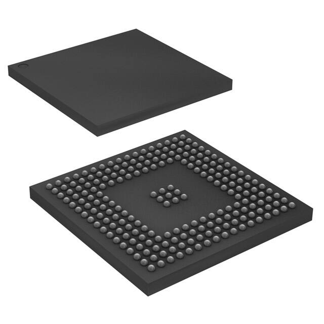


 工商网监
湘ICP备2023018690号
工商网监
湘ICP备2023018690号

