ATA6286C
Embedded AVR Microcontroller with LF Receiver and
UHF Transmitter
DATASHEET
Features
● 8-bit Atmel® AVR® RISC low-power microcontroller
● Embedded ultra-low-power flash 8-bit AVR (Atmel ATA6289) with on-chip sensitive
LF receiver, temperature sensor and integrated UHF transmitter IC
● 8KB of in-system self-programmable Flash memory and 320 Bytes of EEPROM
● 8-bit AVR RISC low-power microcontroller requires typically < 0.5µA sleep current
with active interval timer
● 8mA active current requested at 6dBm output power in transmission mode within
432MHz to 448MHz (Atmel ATA5757) frequency range
● ASK and FSK modulation with up to 20Kbaud data rate in Manchester mode
● Programmable 125kHz wake-up receiver channel with typically 2.3µA current
consumption in listening mode
● Typically 25mbar ADC resolution (measured with a typical pressure sensor)
● Low-power measurement mode for directly connected capacitive sensors with
typically 350µA in 30ms
● Three interfaces for simple capacitive sensors (3pF to 16pF)
● One interface can be configured for motion wake-up (1pF to 4pF)
● Operation voltage 2V to 3.6V for single Li-Cell power supply
● Operating temperature –40°C to +85°C and storage temperature –40°C to +85°C
● Less than 10 external passive components
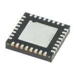
● QFN 32 (5 x 5) package
Applications
● Active RFID
● Access control
9308C-RFID-09/14
�1.
Description
The Atmel® ATA6286C is a embedded ultra-low-power AVR 8-bit microcontroller ICs with integrated RF transmission and LF
receiving functionality for wake-up purposes in a small QFN32 package.
The RF transmission is based on well-known Atmel IPs for 432MHz to 448MHz (Atmel ATA5757) frequency range with a
typical output power up to 6dBm. They are suited for ASK and FSK modulation with up to 20Kbaud data rate in Manchester
mode.
The integrated programmable 125kHz LF receiver channel has extremely low current consumption in active listening mode.
As a result, the LF receiver is particularly well suited for wake-up purposes.
The programmable AVR 8-bit Flash microcontroller includes 8KB of in-system self-programmable Flash memory and 320
bytes of EEPROM thus allowing the system integrator to install field programmable firmware to meet flexible system
requirements on different platforms. The Atmel ATA6286C is configurable to meet extremely low-power requests in sleep
mode, measurement mode and transmission mode.
Furthermore, a low-power interval timer and brown-out detector is integrated.
The Atmel ATA6286Cis suited for powering single cell battery applications. Therefore, a single LiMnO2 battery coin cell can
supply a whole system.
The AVR 8-bit Flash microcontroller also delivers a dedicated integrated simple capacitive sensor interface, as well as an
on-chip calibratable temperature sensor.
Three sensor interfaces are available for capacitive sensing in a range of 3pF to 16pF. In addition, one channel can be
configured for motion sensing in a range of 1pF to 4pF.
The Atmel ATA6286C is thus proposed for applications requiring very extreme low-power consumption such as active RFID
tags with an extended service life.
Owing to the integrated capacitive sensor interface, these ICs may also be used in pressure sensor applications.
2
ATA6286C [DATASHEET]
9308C–RFID–09/14
�2.
Overview
2.1
Block Diagram
VSRF
VCC
PB7 (NSS)
PB5 (SCK)
PB4 (MISO)
PB3 (MOSI)
Figure 2-1. Atmel ATA6286C Block Diagram (MCP)
CLOCK
LF1
LF2
LF Receiver
125 kHz
ECIN1
SPI
Oscillator
Voltage
monitor
EEPROM
Clock
management
and
monitoring
XTO
S0
S1
S2
PC2
PC1
PC0
XTO2
PLL
Timer block
Watchdog
oscillator
ASK
RF
Transmitter
AVR Core
Sensor
interface/
input
multiplexer
FSK
Watchdog
timer
EN
GND
PD7 (SDIN)
PD1 (T3I)
debugWIRE
PD2 (INTO)
PB6
PD0 (T2ICP)
PB2 (T2I)
PB1 (T3O)
PB0 (T3ICP)
IO Ports
Flash
Power
Supervision
POR/ BOD/
TSD and
RESET
VCO
Power
amplifier
ANT1
ANT2
GNDRF
SRAM
RESET
Temperature
sensor
2.2
XTO1
Bonding Diagram
The Atmel® ATA6286C is a smart RF microtransmitter-based multichip package (MCP). Figure 2-2 on page 4 shows the
internal assembly of the MCP. This assembly has two internal dies with four inter-die connections, as shown in Table 2-1.
Table 2-1.
Inter-Die Connection Description of the MCP
Atmel ATA6289 Pin
Atmel ATA5757 Pin
PD3 (INT1) – External Interrupt Input 1
EN – Enable Input
PD4 (ECIN1) – External Clock Input 1
CLK – Clock Output Signal
PD5 (T2O1) – Timer2 Modulator Output 1
ASK – Input Signal
PD6 (T2O2) – Timer2 Modulator Output 2
FSK – Input Signal
ATA6286C [DATASHEET]
9308C–RFID–09/14
3
�Figure 2-2. Multichip Package (MCP)
S1
S0
GND
RESET GNDRF VSRF
XTO1
PB2/
T2I
XTO2
PD3
S2
PB7/
NSS
SGND
ENABLE
LF1
CLK
PB6
ATA5757
PB1/
T3O
ASK FSK
LF2/GND
ANT1
VCC
ATA6289
ANT2
PC2
T2O2
T2O1
ECIN1
PC1
SDIN
PB5/
SCK
PB4/
1 MISO
PC0
PD0/
PD1/
T2ICP T3I
2.3
PB0/
GND
T3ICP
PD7/
SDIN
GND
PD2/
INT0
Pin Configurations
S2
ATA6286C [DATASHEET]
9308C–RFID–09/14
PB2 (T2I)
XTO1
VSRF
GND
RESET
GND
16 15 14 13 12 11 10 9
8
17
XTO2
SGND
18
7
PB7 (NSS)
LF1
19
6
PB6
LF2 (GND)
20
5
PB1 (T3O)
VCC
21
4
ANT1
PC2
22
3
ANT2
PC1
23
2
PB5 (SCK)
PC0
1
24
25 26 27 28 29 30 31 32
PD2 (INTO)
PB3 (MOSI)
GND
PD7 (SDIN)
GND
PB0 (T3ICP)
PD1 (T3I)
Atmel
ATA6286C
PD0 (T2ICP)
4
S0
S1
Figure 2-3. Pinout for QFN32 5mm × 5mm Package
PB4 (MISO)
PB3/
MOSI
�Table 2-2.
Pin Description
Pin
Symbol
Alternate
Function 1
Alternate
Function 2
1
PB4
MISO
PCINT4
SPI
Port B4
2
PB5
SCK
PCINT5
SPI
Port B5
3
ANT2
-
-
RF antenna 2, emitter of antenna output stage
RF pin
4
ANT1
-
-
RF antenna 1, open collector antenna output
RF pin
5
PB1
T3O
PCINT1
Timer3 output
Port B1
6
PB6
-
PCINT6
7
PB7
SS
PCINT7
8
XT02
-
-
9
PB2
T2I
PCINT2
10
XT01
-
11
VSRF
-
12
GNDRF
13
Function
Comment
Port B6
SPI
Port B7
Switch for FSK modulation
RF pin
Timer1, timer2, timer3 external input clock
Port B2
-
Connection for crystal
RF pin
-
Power supply voltage for RF
RF pin
-
-
Power supply ground for RF
RF pin
RESET
debugWIRE
-
Reset input / debugWIRE interface
14
GND
-
-
Power supply ground
15
S0
-
-
Sensor input 0 – pressure sensor (cap.)
16
S1
-
-
Sensor input 1 – sensor (cap.)
17
S2
-
-
Sensor input 2 – motion sensor (cap.) wake-up
18
SGND
-
-
Sensor ground
19
LF1
-
-
LF receiver input 1
20
LF2 / GND
-
-
LF receiver input 2 internally to GND
21
VCC
-
-
Power supply voltage (analog + digital)
22
PC2
-
PCINT10
-
Port C2
23
PC1
CLKO
PCINT9
System clock output
Port C1
24
PC0
ECIN0
PCINT8
External clock input 0
Port C0
25
PD0
T2ICP
PCINT16
Timer2 external input capture
Port D0
26
PD1
T3I
PCINT17
Timer1, timer2, timer3 external input clock
Port D1
27
PB0
T3ICP
PCINT0
Timer3 external input capture
Port B0
28
GND
-
-
Power supply ground
GND
-
-
Power supply ground
29
External interrupt 1 → inter-die connection
(1)
Inter-die
PD3
INT1
PCINT19
Inter-die(1)
PD4
ECIN1
PCINT20
(1)
PD5
T2O1
PCINT21
(1)
PD6
T2O2
PCINT22
Timer2 modulator output 2 → inter-die connection
Port D6
30
PD7
SDIN
PCINT23
SSI – serial data input
Port D7
31
PD2
INT0
PCINT18
External interrupt input 0
Port D2
SPI
Port B3
Inter-die
Inter-die
32
Note:
1.
PB3
MOSI
PCINT3
Internal inter-die connection of the MCP
External clock input 1 → inter-die connection
Timer2 modulator output 1 → inter-die connection
Port D2
Port D4
Port D5
ATA6286C [DATASHEET]
9308C–RFID–09/14
5
�2.4
Pin Names
2.4.1
VCC
Supply voltage
2.4.2
GND
Ground
2.4.3
Port B (PB7..0)
Port B is an 8-bit bi-directional I/O port with internal pull-up resistors (selected for each bit). The port B output buffers have
symmetrical drive characteristics with both high-sink and source-current capability. As inputs, port B pins that are pulled low
externally will source current if the pull-up resistors are activated. The port B pins are tri-stated when a reset condition
becomes active, even if the clock is not running. Port B also serves the functions of various special ATA6289 features as
listed in Section 3.12.3.1 “Alternate Functions of Port B” on page 51.
2.4.4
Port C (PC2..0)
Port C is a 3-bit bi-directional I/O port with internal pull-up resistors (selected for each bit). The port C output buffers have
symmetrical drive characteristics with both high-sink and source-current capability. As inputs, port C pins that are pulled low
externally will source current if the pull-up resistors are activated. The port C pins are tri-stated when a reset condition
becomes active, even if the clock is not running. Port C also serves the functions of various special ATA6289 features as
listed in Section 3.12.3.3 “Alternate Functions of Port C” on page 53.
2.4.5
Port D (PD7..0)
Port D is a 8(4)-bit bi-directional I/O port with internal pull-up resistors (selected for each bit). The PD(6..3) pins are used as
internal inter-die connections I/O ports. The port D output buffers have symmetrical drive characteristics with both high-sink
and source-current capability. As inputs, port D pins that are pulled low externally will source current if the pull-up resistors
are activated. The port D pins are tri-stated when a reset condition becomes active, even if the clock is not running. Port D
also serves the functions of various ATA6289 features as listed in Section 3.12.3.4 “Alternate Functions of Port D” on page
54.
2.4.6
RESET
Reset input. A low level on this pin for longer than the minimum pulse length generates a reset, even if the clock is not
running. The minimum pulse length is given in Table 3-13 on page 35. Shorter pulses do not ensure that a reset is
generated.
2.4.7
LF (2..1)
Input coil pins for the LF receiver.
2.4.8
S (2..0)
Measuring input pins for external capacitance sensor elements.
2.4.9
ANT(2, 1)
RF antenna pins.
2.4.10 XTO(0, 1)
External crystal pins for the internal RF transmitter IC.
2.5
Disclaimer
Typical values contained in this datasheet are based on simulations and the characterization of other AVR microcontrollers
manufactured based on the same process technology. Minimum and maximum values become available after device
characterization.
6
ATA6286C [DATASHEET]
9308C–RFID–09/14
�3.
AVR Microcontroller ATA6289
3.1
Features
●
●
●
●
●
●
●
●
●
High performance, extremely low-power Atmel AVR 8-bit microcontroller
Advanced RISC architecture
●
131 powerful instructions
●
32 × 8 general purpose working registers
●
Fully static operation
●
On-chip 2-cycle multiplier
Non-volatile program and data memories
●
8KB of in-system self-programmable Flash
●
Optional boot code section with independent lock bits
●
320 (256 + 64) bytes of EEPROM
●
512-byte internal SRAM
●
Programming lock for software security
Peripheral features
●
Programmable watchdog/interval timer with separate internal calibrated extremely low-power oscillator
●
Two 16-bit timer/counter with compare mode, capture mode, and on-chip digital data modulator circuitry
●
Integrated (not calibrated) on-chip temperature sensor with thermal shutdown function
●
Sensor interface for external pressure sensor and motion sensor with wake-up function
●
Highly sensitive 1D LF receiver
●
Programmable voltage monitor
●
System clock management and clock monitoring
●
Master/Slave SPI serial interface
●
Integrated debug-wire-interface
●
Interrupt and wake-up on pin change
Special microcontroller features
●
Power-on reset and programmable brown-out detection
●
Internal calibrated RC oscillator
●
External and internal interrupt sources
●
Three sleep modes: idle, sensor noise reduction, and power-down
I/O and package
●
15 (19) programmable I/O lines
●
QFN32 package, 5mm × 5mm
Operating voltage
●
1.9V to 3.6V for ADC and LF receiver
●
1.8V to 3.6V all other components
Speed
●
0 to 2MHz (system clock CLK)
●
0 to 4MHz (timer clock CLT)
Temperature range
●
–40°C to +85°C
ATA6286C [DATASHEET]
9308C–RFID–09/14
7
�3.2
Overview
The Atmel® ATA6289 is a CMOS 8-bit microcontroller with extremely low-power consumption based on the Atmel AVR®
enhanced RISC architecture. By executing powerful instructions in a single clock cycle, the ATA6289 achieves throughputs
approaching 1MIPS per MHz allowing the designer to optimize power consumption versus processing speed.
3.3
Block Diagram
Figure 3-1. Block Diagram of Atmel ATA6289
Oscillator
circuit
Watchdog
timer 0
Clock
management
and monitoring
Watchdog
oscillator
EEPROM
SRAM
Power
Supervision
POR/ BOD/
TSD and
RESET
VCC
GND
RESET
Flash
debugWIRE
AVR Core
Program
logic
AVCC
16 bit T/ C2
12 bit T1
Sensor value
processing
AGND
8
ATA6286C [DATASHEET]
9308C–RFID–09/14
16 bit T/ C3
Temperature
sensor
MUX and
sensor input
SPI
LF receiver
Voltage
monitor
PORT C (x)
PORT B (x)
PORT D (x)
�The Atmel® AVR® core combines a rich instruction set with 32 general purpose working registers. All 32 registers are directly
connected to the Arithmetic Logic Unit (ALU) allowing two independent registers to be accessed in one single instruction
executed in one clock cycle. The resulting architecture is more code-efficient while achieving throughputs up to ten times
faster than conventional CISC microcontrollers.
The Atmel ATA6289 provides the following features: 8KB of in-system programmable Flash with read-while-write
capabilities, 320 (256+64) bytes of EEPROM, 512 bytes of SRAM, 15 (19) general purpose I/O lines, 32 general purpose
working registers, on-chip debugging support and programming, three flexible timers/counters, two of them with compare
modes, internal and external interrupts, a sensor interface for the external pressure sensor and an acceleration/motion
sensor, a programmable watchdog timer with internally calibrated oscillator, an SPI serial port, and three software-selectable
power-saving modes.
The device is manufactured using Atmel high-density non-volatile memory technology. On-chip ISP Flash allows the
program memory to be reprogrammed in-system through an SPI serial interface, by a conventional non-volatile memory
programmer, or by an on-chip boot program running on the Atmel AVR core. The boot program can use any interface to
download the application program in the application Flash memory. Software in the boot Flash section continues to run while
the application Flash section is updated, providing true read-while-write operation. By combining an 8-bit RISC CPU with insystem self-programmable Flash on a monolithic chip, the Atmel ATA6289 is a powerful microcontroller that provides a
highly flexible and cost effective solution to many embedded control applications.
The Atmel ATA6289 AVR is supported with a full suite of program and system development tools including: C compilers,
macro assemblers, program debugger/simulators, in-circuit emulators, and evaluation kits.
3.4
About Code Examples
This documentation contains simple code examples that briefly show how to use various parts of the device. These code
examples assume that the part-specific header file is included before compilation. Be aware that not all C compiler vendors
include bit definitions in the header files and interrupt handling in C is compiler-dependent. Please refer to the C compiler
documentation for more details.
The Atmel AVR Studio® can be used for code development. Please select the Atmel AVR device “ATA6289.”
ATA6286C [DATASHEET]
9308C–RFID–09/14
9
�3.5
Atmel AVR CPU Core
3.5.1
Architectural Overview
Figure 3-2. Block Diagram of the Atmel AVR Architecture
Data Bus 8-bit
Flash
Program
Me m or y
Program
Counter
Status and
Control
32 x 8
General
Purpose
Registers
Instruction
Register
Lines
Addressing
ALU
Indirect
Control
SPI
Unit
Watchdog
Tim e r
Direct Addressing
Instruction
Decoder
Interrupt
Unit
Clock
Management
LFReceiver
Data
SRAM
I/O Module 1
EEPROM
I/O Module n
I/O Lines
In order to maximize performance and parallelism, the Atmel® AVR® uses Harvard architecture with separate memories and
buses for program and data. Instructions in the program memory are executed with single level pipelining. While one
instruction is being executed, the next instruction is pre-fetched from the program memory. This concept enables instructions
to be executed in every clock cycle. The program memory is in-system reprogrammable Flash memory.
The fast-access register file contains 32 x 8-bit general purpose working registers with a single clock cycle access time. This
allows single-cycle ALU operation. In a typical ALU operation, two operands are output from the register file, the operation is
executed and the result is stored back in the register file—all in one clock cycle.
Six of the 32 registers can be used as three 16-bit indirect address-register pointers for data space addressing—enabling
efficient address calculations. One of these address pointers can also be used as an address pointer to look up tables in the
Flash program memory. These added function registers are the 16-bit X, Y and Z registers described later in this section.
The ALU supports arithmetic and logic operations between registers or between a constant and a register. Single-register
operations can also be executed in the ALU. After an arithmetic operation, the status register is updated to reflect
information about the operation outcome.
10
ATA6286C [DATASHEET]
9308C–RFID–09/14
�Program flow is enabled by conditional and unconditional jump and call instructions, allowing the entire address space to be
addressed directly. Most Atmel® AVR® instructions have a single 16-bit word format. Every program memory address
contains a 16- or 32-bit instruction.
Program Flash memory space is divided into two sections, the boot program section and the application program section.
Both sections have dedicated lock bits for write and read/write protection. The Store Program Memory (SPM) instruction that
writes into the application Flash memory section must reside in the boot program section.
During interrupts and subroutine calls, the return address Program Counter (PC) is stored on the stack. The stack is
effectively allocated in the general data SRAM, and consequently the stack size is only limited by the total SRAM size and
the usage of the SRAM. All user programs must initialize the Stack Pointer (SP) in the reset routine (before subroutines or
interrupts are executed). The SP is read/write-accessible in the I/O space. The data SRAM can be accessed easily through
the five different addressing modes supported in the Atmel AVR architecture.
The memory spaces in the Atmel AVR architecture are all linear and regular memory maps.
A flexible interrupt module has its control registers in the I/O space with an additional global interrupt enable bit in the status
register. All interrupts have a separate interrupt vector in the interrupt vector table. The interrupts have priority in accordance
with their interrupt vector position. The lower the interrupt vector address, the higher the priority.
The I/O memory space contains 64 addresses for CPU peripheral functions as control registers, SPI and other I/O functions.
The I/O memory can be accessed directly, or as the data space locations following those of the register file, 0x20 - 0x5F. In
addition, the ATA6289 has extended I/O space from 0x60 - 0xFF in SRAM where only the ST/STS/STD and LD/LDS/LDD
instructions can be used.
3.5.2
ALU – Arithmetic Logic Unit
The high-performance Atmel AVR ALU operates in direct connection with all 32 general purpose working registers. Within a
single clock cycle, arithmetic operations between general purpose registers or between a register and an immediate are
executed. The ALU operations are divided into three main categories—arithmetic, logic and bit-functions. Some
implementations of the architecture also provide a powerful multiplier supporting both signed/unsigned multiplication and
fractional format. For a detailed description, see Section 3.22 “Instruction Set Summary” on page 156.
3.5.3
Status Register
The status register contains information about the result of the most recently executed arithmetic instruction. This
information can be used for altering the program flow in order to perform conditional operations. Note that the status register
is updated after all ALU operations, as specified in the instruction set reference. In many cases—this eliminates the need to
use the dedicated compare instructions, resulting in faster and more compact code. The status register is not automatically
stored when entering an interrupt routine and restored when returning from an interrupt.This must be handled by software.
3.5.3.1 The Atmel AVR Status Register (SREG):
Bit
7
6
5
4
3
2
1
0
I
T
H
S
V
N
Z
C
Read/Write
R/W
R/W
R/W
R/W
R/W
R/W
R/W
R/W
Initial Value
0
0
0
0
0
0
0
0
SREG
Bit 7 – I: Global Interrupt Enable
The global interrupt enable bit must be set for the interrupts to be enabled. The individual interrupt enable control is then
performed in separate control registers. If the global interrupt enable register is cleared, none of the interrupts are enabled
independently of the individual interrupt enable settings. The I bit is cleared by hardware after an interrupt has occurred, and
is set by the RETI instruction to enable subsequent interrupts. The I bit can also be set and cleared by the application with
the SEI and CLI instructions, as described in the instruction set reference.
Bit 6 – T: Bit Copy Storage
The bit copy instructions BLD (Bit LoaD) and BST (Bit STore) use the T bit as the source or destination for the operated bit.
A bit from a register in the register file can be copied into T by the BST instruction, and a bit in T can be copied by the BLD
instruction into a bit in a register in the register file.
Bit 5 – H: Half Carry Flag
The half carry flag H indicates a half carry in some arithmetic operations. Half carry is useful in BCD arithmetic. See Section
3.22 “Instruction Set Summary” on page 156 for detailed information.
ATA6286C [DATASHEET]
9308C–RFID–09/14
11
�Bit 4 – S: Sign Bit, S = N ⊕ V
The S bit is always exclusive or located between the negative flag N and the two’s complement overflow flag V. See Section
3.22 “Instruction Set Summary” on page 156 for detailed information.
Bit 3 – V: Two’s Complement Overflow Flag
The two's complement overflow flag V supports two's complement arithmetic. See Section 3.22 “Instruction Set Summary”
on page 156 for detailed information.
Bit 2 – N: Negative Flag
The negative flag N indicates a negative result in an arithmetic or logic operation. See Section 3.22 “Instruction Set
Summary” on page 156 for detailed information.
Bit 1 – Z: Zero Flag
The zero flag Z indicates a zero result in an arithmetic or logic operation. See Section 3.22 “Instruction Set Summary” on
page 156 for detailed information.
Bit 0 – C: Carry Flag
The carry flag C indicates a carry in an arithmetic or logic operation. See Section 3.22 “Instruction Set Summary” on page
156 for detailed information.
3.5.4
General Purpose Register File
The register file is optimized for the Atmel® AVR® enhanced RISC instruction set. In order to achieve the required
performance and flexibility, the following input/output schemes are supported by the register file:
• One 8-bit output operand and one 8-bit result input
• Two 8-bit output operands and one 8-bit result input
• Two 8-bit output operands and one 16-bit result input
• One 16-bit output operand and one 16-bit result input
Figure 3-3 shows how the 32 general purpose working registers in the CPU are structured.
Figure 3-3. Atmel AVR CPU General Purpose Working Registers
Bit:
7
0
Addr.
R0
0x00
R1
0x01
R2
0x02
…
R13
0x0D
General
R14
0x0E
Purpose
R15
0x0F
Working
R16
0x10
Registers
R17
0x11
…
R26
0x1A
X register low byte
R27
0x1B
X register high byte
R28
0x1C
Y register low byte
R29
0x1D
Y register high byte
R30
0x1E
Z register low byte
R31
0x1F
Z register high byte
Most of the instructions operating on the register file have direct access to all registers, and most of them are single-cycle
instructions. As shown in Figure 3-3, each register is also assigned a data memory address, mapping them directly into the
first 32 locations of the user data space. Although not physically implemented as SRAM locations, this memory organization
provides considerable flexibility in accessing the registers because the X-, Y- and Z-pointer registers can be set to index any
register in the file.
12
ATA6286C [DATASHEET]
9308C–RFID–09/14
�3.5.4.1 The X, Y and Z Registers
The registers R26..R31 have some added functions to their general purpose usage. These registers are 16-bit address
pointers for indirect addressing of the data space. The three indirect address registers X, Y and Z are defined as described
in Figure 3-4.
Figure 3-4. The X, Y and Z Registers
X Register
15
XH
XL
0
7
0
7
0
R27(0x1B)
Y Register
R26 (0x1A)
15
YH
YL
0
7
0
7
0
R29 (0x1D)
Z Register
R28 (0x1C)
15
ZH
ZL
0
7
0
7
0
R31 (0x1F)
R30 (0x1E)
In the different addressing modes these address registers have functions as fixed displacement, automatic increment and
automatic decrement (see the instruction set reference for more information.)
3.5.5
The Stack Pointer
The stack is primarily used for storing temporary data, for storing local variables and for storing return addresses after
interrupts and subroutine calls. The stack pointer register always points to the top of the stack. Note that the stack is
implemented as growing from higher memory locations to lower memory locations. This implies that a stack PUSH command
decreases the stack pointer.
The stack pointer points to the data SRAM stack area where the subroutine and interrupt stacks are located. This stack
space in the data SRAM must be defined by the program before any subroutine calls are executed or interrupts are enabled.
The stack pointer must be set to point above 0x100, preferably RAMEND. The stack pointer is decremented by one when
data is pushed onto the stack with the PUSH instruction, and it is decremented by two when the return address is pushed
onto the stack with a subroutine call or interrupt. The stack pointer is incremented by one when data is popped from the
stack with the POP instruction, and it is incremented by two when the return address is popped from the stack with return
from subroutine RET or return from interrupt RETI.
The Atmel® AVR® Stack Pointer is implemented as two 8-bit registers in the I/O space. The number of bits actually used is
implementation-dependent. Note that the data space in some implementations of the Atmel AVR architecture is so small that
only SPL is needed. In this case, the SPH register is not present.
In ATA6289 only SP9 and Sp8 of high byte (SPH) are used.
Bit
15
14
13
12
11
10
9
8
SP15
SP14
SP13
SP12
SP11
SP10
SP9
SP8
SPH
SP7
SP6
SP5
SP4
SP3
SP2
SP1
SP0
SPL
Bit
7
6
5
4
3
2
1
0
Read/Write
R/W
R/W
R/W
R/W
R/W
R/W
R/W
R/W
R/W
R/W
R/W
R/W
R/W
R/W
R/W
R/W
Initial Value
RAMEND RAMEND RAMEND RAMEND RAMEND RAMEND RAMEND RAMEND
RAMEND RAMEND RAMEND RAMEND RAMEND RAMEND RAMEND RAMEND
ATA6286C [DATASHEET]
9308C–RFID–09/14
13
�3.5.6
Instruction Execution Timing
This section describes the general access timing concepts for instruction execution. The Atmel® AVR® CPU is driven by the
CPU clock, CLKCPU, directly generated from the selected clock source for the chip. No internal clock division is used.
Figure 3-5 shows the parallel instruction fetches and instruction executions enabled by the Harvard architecture and the fastaccess register file concept. This is the basic pipelining concept to obtain up to 1MIPS per MHz with the corresponding
unique results for functions per cost, functions per clocks and functions per power unit.
Figure 3-5. The Parallel Instruction Fetches and Instruction Executions
T1
T2
T3
T4
clkCPU
1st Instruction Fetch
1st Instruction Fetch
2nd Instruction Fetch
2nd Instruction Fetch
3rd Instruction Fetch
3rd Instruction Fetch
4th Instruction Fetch
Figure 3-6 shows the internal timing concept for the register file. In a single clock cycle an ALU operation using two register
operands is executed with the result stored to the destination register.
Figure 3-6. Single-Cycle ALU Operation
T1
T2
T3
T4
clkCPU
Total Execution Time
Register Operands Fetch
ALU Operation Execute
Result Write Back
3.5.7
Reset and Interrupt Handling
The Atmel AVR provides several different interrupt sources. These interrupts and the separate reset vector each have a
separate program vector in the program memory space. All interrupts are assigned unique enable bits which must be written
logic one together with the global interrupt enable bit in the status register in order to enable the interrupt. Depending on the
program counter value, interrupts may be automatically disabled when boot lock bits BLB02 or BLB12 are programmed. This
feature improves software security. See Section 3.19.5.1 “Store Program Memory Control and Status Register – SPMCSR”
on page 136 for more details.
By default the lowest addresses in the program memory space are defined as the reset and interrupt vectors. The complete
list of vectors is found in Section 3.10 “Interrupts” on page 39. This list also determines the priority levels of the different
interrupts. The lower the address the higher the priority level. RESET has the highest priority, followed by INT0—the external
interrupt request 0. The interrupt vectors can be moved to the start of the boot Flash section by setting the IVSEL bit in the
MCU Control Register (MCUCR). For more information, see Section 3.10 “Interrupts” on page 39. The reset vector can also
be moved to the start of the boot Flash section by programming the BOOTRST fuse. See Section 3.19 “Boot Loader Support
– Read-While-Write Self-Programming” on page 126 for more details.
When an interrupt occurs, the global interrupt enable I bit is cleared and all interrupts are disabled. The user software can
write logic one to the I bit to enable nested interrupts. All enabled interrupts can then interrupt the current interrupt routine.
The I bit is automatically set when a Return from Interrupt instruction (RETI) is executed.
14
ATA6286C [DATASHEET]
9308C–RFID–09/14
�There are basically two types of interrupts. The first type is triggered by an event that sets the interrupt flag. For these
interrupts, the program counter is vectored to the actual interrupt vector in order to execute the interrupt handling routine,
and hardware clears the corresponding interrupt flag. Interrupt flags can also be cleared by writing a logic one to the flag bit
position(s) to be cleared. If an interrupt condition occurs while the corresponding interrupt enable bit is cleared, the interrupt
flag is set and remembered until the interrupt is enabled, or the flag is cleared by software. Similarly, if one or more interrupt
conditions occur while the global interrupt enable bit is cleared, the corresponding interrupt flag(s) is set and remembered
until the global interrupt enable bit is set, and is then executed by order of priority.
The second type of interrupts triggers as long as the interrupt condition is present. These interrupts do not necessarily have
interrupt flags. If the interrupt condition disappears before the interrupt is enabled, the interrupt is not triggered.
When the Atmel AVR exits from an interrupt, it always returns to the main program and executes one more instruction before
any pending interrupt is served.
Note that the status register is not automatically stored when entering an interrupt routine, and not restored when returning
from an interrupt routine. This must be handled by software.
When using the CLI instruction to disable interrupts, interrupts are immediately disabled. No interrupt is executed after the
CLI instruction, even if it occurs simultaneously with the CLI instruction. The following example shows how this can be used
to avoid interrupts during the timed EEPROM write sequence.
Assembly Code Example
inr16, SREG; store SREG value
cli ; disable interrupts during timed sequence
sbiEECR, EEMWE; start EEPROM write
sbiEECR, EEWE
outSREG, r16; restore SREG value (I-bit)
C Code Example
char cSREG;
cSREG = SREG;/* store SREG value */
/* disable interrupts during timed sequence */
_CLI();
EECR |= (1


 工商网监
湘ICP备2023018690号
工商网监
湘ICP备2023018690号
