ATA6622C/ATA6624C/ATA6626C
LIN Bus Transceiver with 3.3V (5V) Regulator and
Watchdog
DATASHEET
Features
● Master and slave operation possible
● Supply voltage up to 40V
● Operating voltage VS = 5V to 27V
● Typically 10µA supply current during Sleep Mode
● Typically 57µA supply current in Silent Mode
● Linear low-drop voltage regulator, 85mA current capability:
● Normal, Fail-safe, and Silent Mode
● Atmel ATA6622C VCC = 3.3V ±2%
● Atmel ATA6624C VCC = 5.0V ±2%
● Atmel ATA6626C VCC = 5.0V ±2%, TXD time-out timer disabled
● In Sleep Mode VCC is switched off
● VCC- undervoltage detection (4ms reset time) and watchdog reset logical
combined at open drain output NRES
● Negative trigger input for watchdog
● Boosting the voltage regulator possible with an external NPN transistor
● LIN physical layer according to LIN 2.0, 2.1 and SAEJ2602-2
● Wake-up capability via LIN-bus, wake pin, or Kl_15 pin
● INH output to control an external voltage regulator or to switch off the master pull
up resistor
● TXD time-out timer; Atmel ATA6626C: TXD time-out timer Is disabled
● Bus pin is overtemperature and short circuit protected versus GND and battery
● Adjustable watchdog time via external resistor
● Advanced EMC and ESD performance
● Fulfills the OEM “Hardware Requirements for LIN in automotive Applications
Rev.1.0”
● Interference and damage protection according to ISO7637
● Qualified according to AEC-Q100
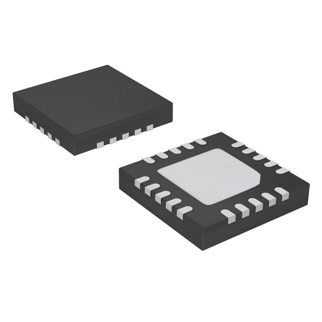
● Package: QFN 5mm x 5mm with 20 pins (Moisture Sensitivity Level 1)
4986O-AUTO-10/14
�1.
Description
The Atmel® ATA6622C is a fully integrated LIN transceiver, which complies with the LIN 2.0, 2.1 and SAEJ2602-2
specifications. It has a low-drop voltage regulator for 3.3V/85mA output and a window watchdog. The Atmel ATA6624C has
the same functionality as the Atmel ATA6622C; however, it uses a 5V/85mA regulator. The Atmel ATA6626C has the same
functionality as Atmel ATA6624C without a TXD time-out timer. The voltage regulator is able to source 85mA, but the output
current can be boosted by using an external NPN transistor. This chip combination makes it possible to develop inexpensive,
simple, yet powerful slave and master nodes for LIN-bus systems. Atmel ATA6622C/ATA6624C/ATA6626C are designed to
handle the low-speed data communication in vehicles, e.g., in convenience electronics. Improved slope control at the LINdriver ensures secure data communication up to 20kBaud. Sleep Mode and Silent Mode guarantee very low current
consumption. The Atmel ATA6626C is able to switch the LIN unlimited to dominant level via TXD for low data rates.
Figure 1-1. Block Diagram
20
VS
Normal and
Fail-safe
Mode
10
INH
PVCC
Normal
Mode
Receiver
-
9
RXD
+
7
RF Filter
LIN
4
WAKE
16
KL_15
PVCC
Edge
Detection
Wake-up
Bus Timer
Slew Rate Control
TXD
Time-out
Timer
11
TXD
Short Circuit and
Overtemperature
Protection
*)
Control Unit
EN
GND
1
5
OUT
Internal Testing
Unit
15
MODE
14
Watchdog
3
TM
*) Not in ATA6626
ATA6622C/ATA6624C/ATA6626C [DATASHEET]
4986O–AUTO–10/14
18
NTRIG
VCC
PVCC
12
Undervoltage
Reset
PVCC
2
19
Normal/Silent/
Fail-safe Mode
3.3/5V
NRES
Adjustable
Watchdog
Oscillator
13
WD_OSC
�Pin Configuration
Table 2-1.
VCC
PVCC
GND
KL15
20
19
18
17
16
1
3
WAKE
4
GND
5
QFN 5mm x 5mm
0.65mm pitch
20 lead
6
7
8
9
10
INH
NTRIG
RXD
2
GND
GND
ATA6622C
ATA6624C
ATA6626C
LIN
EN
VS
Figure 2-1. Pinning QFN20
GND
2.
15
MODE
14
TM
13
WD_OSC
12
NRES
11
TXD
Pin Description
Pin
Symbol
1
EN
Function
Enables the device in Normal Mode
2
GND
3
NTRIG
System ground (optional)
Low-level watchdog trigger input from microcontroller
4
WAKE
High-voltage input for local wake-up request; if not needed, connect directly to VS
5
GND
System ground (mandatory)
6
GND
System ground (optional)
7
LIN
LIN-bus line input/output
8
GND
System ground (optional)
9
RXD
Receive data output
10
INH
Battery related output for controlling an external voltage regulator
11
TXD
Transmit data input; active low output (strong pull down) after a local wake-up request
12
NRES
13
WD_OSC
Output undervoltage and watchdog reset (open drain)
External resistor for adjustable watchdog timing
14
TM
15
MODE
Low, watchdog is on; high, watchdog is off
16
KL_15
Ignition detection (edge sensitive)
17
GND
System ground (optional)
18
PVCC
3.3V/5V regulator sense input pin
19
VCC
3.3V/5V regulator output/driver pin
20
VS
Backside
For factory testing only (tie to ground)
Battery supply
Heat slug is connected to all GND pins
ATA6622C/ATA6624C/ATA6626C [DATASHEET]
4986O–AUTO–10/14
3
�3.
Functional Description
3.1
Physical Layer Compatibility
Since the LIN physical layer is independent from higher LIN layers (e.g., the LIN protocol layer), all nodes with a LIN physical
layer according to revision 2.x can be mixed with LIN physical layer nodes, which, according to older versions (i.e., LIN 1.0,
LIN 1.1, LIN 1.2, LIN 1.3), are without any restrictions.
3.2
Supply Pin (VS)
The LIN operating voltage is VS = 5V to 27V. An undervoltage detection is implemented to disable data transmission if VS
falls below VSth < 4V in order to avoid false bus messages. After switching on VS, the IC starts in Fail-safe Mode, and the
voltage regulator is switched on.
The supply current is typically 10µA in Sleep Mode and 57µA in Silent Mode.
3.3
Ground Pin (GND)
The IC does not affect the LIN Bus in the event of GND disconnection. It is able to handle a ground shift up to 11.5% of VS.
The mandatory system ground is pin 5.
3.4
Voltage Regulator Output Pin (VCC)
The internal 3.3V/5V voltage regulator is capable of driving loads up to 85mA. It is able to supply the microcontroller and
other ICs on the PCB and is protected against overloads by means of current limitation and overtemperature shut-down.
Furthermore, the output voltage is monitored and will cause a reset signal at the NRES output pin if it drops below a defined
threshold Vthun. To boost up the maximum load current, an external NPN transistor may be used, with its base connected to
the VCC pin and its emitter connected to PVCC.
3.5
Voltage Regulator Sense Pin (PVCC)
The PVCC is the sense input pin of the 3.3V/5V voltage regulator. For normal applications (i.e., when only using the internal
output transistor), this pin is connected to the VCC pin. If an external boosting transistor is used, the PVCC pin must be
connected to the output of this transistor, i.e., its emitter terminal.
3.6
Bus Pin (LIN)
A low-side driver with internal current limitation and thermal shutdown and an internal pull-up resistor compliant with the LIN
2.x specification are implemented. The allowed voltage range is between –27V and +40V. Reverse currents from the LIN
bus to VS are suppressed, even in the event of GND shifts or battery disconnection. LIN receiver thresholds are compatible
with the LIN protocol specification. The fall time from recessive to dominant bus state and the rise time from dominant to
recessive bus state are slope controlled.
3.7
Input/Output Pin (TXD)
In Normal Mode the TXD pin is the microcontroller interface used to control the state of the LIN output. TXD must be pulled
to ground in order to have a low LIN-bus. If TXD is high or unconnected (internal pull-up resistor), the LIN output transistor is
turned off, and the bus is in recessive state. During Fail-safe Mode, this pin is used as output. It is current-limited to < 8mA.
and is latched to low if the last wake-up event was from pin WAKE or KL_15.
3.8
TXD Dominant Time-out Function
The TXD input has an internal pull-up resistor. An internal timer prevents the bus line from being driven permanently in
dominant state. If TXD is forced to low for longer than tDOM > 6ms, the LIN-bus driver is switched to recessive state.
To reactivate the LIN bus driver, switch TXD to high (> 10µs).
The time-out function is disabled in the ATA6626C. Switching to dominant level on the LIN bus occurs without any time
limitations.
4
ATA6622C/ATA6624C/ATA6626C [DATASHEET]
4986O–AUTO–10/14
�3.9
Output Pin (RXD)
This output pin reports the state of the LIN-bus to the microcontroller. LIN high (recessive state) is reported by a high level at
RXD; LIN low (dominant state) is reported by a low level at RXD. The output has an internal pull-up resistor with typically
5kΩ to VCC. The AC characteristics can be defined with an external load capacitor of 20pF.
The output is short-circuit protected. RXD is switched off in Unpowered Mode (i.e., VS = 0V).
3.10
Enable Input Pin (EN)
The Enable Input pin controls the operation mode of the device. If EN is high, the circuit is in Normal Mode, with transmission
paths from TXD to LIN and from LIN to RXD both active. The VCC voltage regulator operates with 3.3V/5V/85mA output
capability.
If EN is switched to low while TXD is still high, the device is forced to Silent Mode. No data transmission is then possible, and
the current consumption is reduced to IVS typ. 57µA. The VCC regulator has its full functionality.
If EN is switched to low while TXD is low, the device is forced to Sleep Mode. No data transmission is possible, and the
voltage regulator is switched off.
3.11
Wake Input Pin (WAKE)
The Wake Input pin is a high-voltage input used to wake up the device from Sleep Mode or Silent Mode. It is usually
connected to an external switch in the application to generate a local wake-up. A pull-up current source, typically 10µA, is
implemented.
If a local wake-up is not needed in the application, connect the Wake pin directly to the VS pin.
3.12
Mode Input Pin (MODE)
Connect the MODE pin directly or via an external resistor to GND for normal watchdog operation. To debug the software of
the connected microcontroller, connect MODE pin to 3.3V/5V and the watchdog is switched off.
3.13
TM Input Pin
The TM pin is used for final production measurements at Atmel®. In normal application, it has to be always connected to
GND.
3.14
KL_15 Pin
The KL_15 pin is a high-voltage input used to wake up the device from Sleep or Silent Mode. It is an edge sensitive pin (lowto-high transition). It is usually connected to ignition to generate a local wake-up in the application when the ignition is
switched on. Although KL_15 pin is at high voltage (VBatt), it is possible to switch the IC into Sleep or Silent Mode. Connect
the KL_15 pin directly to GND if you do not need it. A debounce timer with a typical TdbKl_15 of 160µs is implemented.
The input voltage threshold can be adjusted by varying the external resistor due to the input current IKL_15. To protect this pin
against voltage transients, a serial resistor of 47kΩ and a ceramic capacitor of 100nF are recommended. With this RC
combination you can increase the wake-up time TwKL_15 and, therefore, the sensitivity against transients on the ignition
Kl.15.
You can also increase the wake-up time using external capacitors with higher values.
3.15
INH Output Pin
The INH Output pin is used to switch an external voltage regulator on during Normal or Fail-safe Mode. The INH pin is
switched off in Sleep or Silent Mode. It is possible to switch off the external 1kΩ master resistor via the INH pin for master
node applications. The INH pin is switched off during VCC undervoltage reset.
3.16
Reset Output Pin (NRES)
The Reset Output pin, an open drain output, switches to low during VCC undervoltage or a watchdog failure.
ATA6622C/ATA6624C/ATA6626C [DATASHEET]
4986O–AUTO–10/14
5
�3.17
WD_OSC Output Pin
The WD_OSC Output pin provides a typical voltage of 1.2V, which supplies an external resistor with values between 34kΩ
and 120kΩ to adjust the watchdog oscillator time.
3.18
NTRIG Input Pin
The NTRIG Input pin is the trigger input for the window watchdog. A pull-up resistor is implemented. A negative edge triggers
the watchdog. The trigger signal (low) must exceed a minimum time ttrigmin to generate a watchdog trigger.
3.19
Wake-up Events from Sleep or Silent Mode
●
●
●
●
6
LIN-bus
WAKE pin
EN pin
KL_15
ATA6622C/ATA6624C/ATA6626C [DATASHEET]
4986O–AUTO–10/14
�4.
Modes of Operation
Figure 4-1. Modes of Operation
a: VS > 5V
Unpowered Mode
VBatt = 0V
b: VS < 3.7V
c: Bus wake-up event
d: Wake up from WAKE or KL_15 pin
a
b
e: NRES switches to low
b
Fail-safe Mode
VCC: 3.3V/5V
with undervoltage monitoring
Communication: OFF
Watchdog: ON
b
e
EN = 1
b
c+d+e
EN = 1
c+d
Go to silent command
EN = 0
Silent Mode
TXD = 1
Normal Mode
VCC: 3.3V/5V
with undervoltage monitoring
Communication: OFF
Watchdog: OFF
Local wake-up event
EN = 1
VCC: 3.3V/5V
with undervoltage
monitoring
Go to sleep command
EN = 0
Communication: ON
Watchdog: ON
Table 4-1.
VCC: switched off
Communication: OFF
Watchdog: OFF
Table of Modes
Mode of
Operation
4.1
Sleep Mode
TXD = 0
Transceiver
VCC
Watchdog
WD_OSC
INH
RXD
LIN
Recessive
Fail-safe
Off
3.3V/5V
On
1.23V
On
High,
except after wake-up
Normal
On
3.3V/5V
On
1.23V
On
LIN depending
TXD
depending
Silent
Off
3.3V/5V
Off
0V
Off
High
Recessive
Sleep
Off
0V
Off
0V
Off
0V
Recessive
Normal Mode
This is the normal transmitting and receiving mode of the LIN Interface in accordance with the LIN specification LIN 2.x. The
voltage regulator is active and can source up to 85mA. The undervoltage detection is activated. The watchdog needs a
trigger signal from NTRIG to avoid resets at NRES. If NRES is switched to low, the IC changes its state to Fail-safe Mode.
ATA6622C/ATA6624C/ATA6626C [DATASHEET]
4986O–AUTO–10/14
7
�4.2
Silent Mode
A falling edge at EN when TXD is high switches the IC into Silent Mode. The TXD Signal has to be logic high during the
Mode Select window (see Figure 4-2). The transmission path is disabled in Silent Mode. The overall supply current from VBatt
is a combination of the IVSsi = 57µA plus the VCC regulator output current IVCC.
The internal slave termination between the LIN pin and the VS pin is disabled in Silent Mode, only a weak pull-up current
(typically 10µA) between the LIN pin and the VS pin is present. Silent Mode can be activated independently from the actual
level on the LIN, WAKE, or KL_15 pins.
If an undervoltage condition occurs, NRES is switched to low, and the IC changes its state to Fail-safe Mode.
A voltage less than the LIN Pre_Wake detection VLINL at the LIN pin activates the internal LIN receiver and switches on the
internal slave termination between the LIN pin and the VS pin.
Figure 4-2. Switch to Silent Mode
Normal Mode
Silent Mode
EN
TXD
Mode select window
td = 3.2μs
NRES
VCC
Delay time silent mode
td_silent maximum 20μs
LIN
LIN switches directly to recessive mode
8
ATA6622C/ATA6624C/ATA6626C [DATASHEET]
4986O–AUTO–10/14
�A falling edge at the LIN pin followed by a dominant bus level maintained for a certain time period (> tbus) and the following
rising edge at the LIN pin (see Figure 4-3 on page 9) results in a remote wake-up request. The device switches from Silent
Mode to Fail-safe Mode. The remote wake-up request is indicated by a low level at the RXD pin to interrupt the
microcontroller (see Figure 4-3 on page 9). EN high can be used to switch directly to Normal Mode.
Figure 4-3. LIN Wake Up from Silent Mode
Bus wake-up filtering time
tbus
Fail-safe mode
Normal mode
LIN bus
Node in silent mode
RXD
High
Low
High
TXD
Watchdog
VCC
voltage
regulator
Watchdog off
Start watchdog lead time td
Silent mode 3.3V/5V
Fail safe mode 3.3V/5V
Normal mode
EN High
EN
NRES
Undervoltage detection active
ATA6622C/ATA6624C/ATA6626C [DATASHEET]
4986O–AUTO–10/14
9
�4.3
Sleep Mode
A falling edge at EN when TXD is low switches the IC into Sleep Mode. The TXD Signal has to be logic low during the Mode
Select window (Figure 4-4 on page 10). In order to avoid any influence to the LIN-pin during switching into sleep mode it is
possible to switch the EN up to 3.2 µs earlier to LOW than the TXD. Therefore, the best and easiest way are two falling
edges at TXD and EN at the same time.The transmission path is disabled in Sleep Mode. The supply current IVSsleep from
VBatt is typically 10µA.
The VCC regulator is switched off. NRES and RXD are low. The internal slave termination between the LIN pin and VS pin is
disabled, only a weak pull-up current (typically 10µA) between the LIN pin and the VS pin is present. Sleep Mode can be
activated independently from the current level on the LIN, WAKE, or KL_15 pin.
A voltage less than the LIN Pre_Wake detection VLINL at the LIN pin activates the internal LIN receiver and switches on the
internal slave termination between the LIN pin and the VS pin.
A falling edge at the LIN pin followed by a dominant bus level maintained for a certain time period (> tbus) and a following
rising edge at pin LIN results in a remote wake-up request. The device switches from Sleep Mode to Fail-safe Mode.
The VCC regulator is activated, and the remote wake-up request is indicated by a low level at the RXD pin to interrupt the
microcontroller (see Figure 4-5 on page 11).
EN high can be used to switch directly from Sleep/Silent to Fail-safe Mode. If EN is still high after VCC ramp up and
undervoltage reset time, the IC switches to the Normal Mode.
Figure 4-4. Switch to Sleep Mode
Normal Mode
Sleep Mode
EN
Mode select window
TXD
td = 3.2μs
NRES
VCC
Delay time sleep mode
td_sleep = maximum 20μs
LIN
LIN switches directly to recessive mode
10
ATA6622C/ATA6624C/ATA6626C [DATASHEET]
4986O–AUTO–10/14
�4.4
Fail-safe Mode
The device automatically switches to Fail-safe Mode at system power-up. The voltage regulator is switched on (see Figure
5-1 on page 13). The NRES output switches to low for tres = 4ms and gives a reset to the microcontroller. LIN communication
is switched off. The IC stays in this mode until EN is switched to high. The IC then changes to Normal Mode. A power down
of VBatt (VS < 3.7V) during Silent or Sleep Mode switches the IC into Fail-safe Mode after power up. A low at NRES switches
into Fail-safe Mode directly. During Fail-safe Mode the TXD pin is an output and signals the last wake-up source.
4.5
Unpowered Mode
If you connect battery voltage to the application circuit, the voltage at the VS pin increases according to the block capacitor
(see Figure 5-1 on page 13). After VS is higher than the VS undervoltage threshold VSth, the IC mode changes from
Unpowered Mode to Fail-safe Mode. The VCC output voltage reaches its nominal value after tVCC. This time, tVCC, depends
on the VCC capacitor and the load.
The NRES is low for the reset time delay treset. During this time, treset, no mode change is possible.
Figure 4-5. LIN Wake Up from Sleep Mode
Bus wake-up filtering time
tbus
Fail-safe Mode
Low
Low
Normal Mode
LIN bus
RXD
TXD
VCC
voltage
regulator
On state
Off state
Regulator wake-up time
EN High
EN
Reset
time
NRES
Low
Microcontroller
start-up time delay
Watchdog
Watchdog off
Start watchdog lead time td
ATA6622C/ATA6624C/ATA6626C [DATASHEET]
4986O–AUTO–10/14
11
�5.
Wake-up Scenarios from Silent or Sleep Mode
5.1
Remote Wake-up via Dominant Bus State
A voltage less than the LIN Pre_Wake detection VLINL at the LIN pin activates the internal LIN receiver.
A falling edge at the LIN pin followed by a dominant bus level VBUSdom maintained for a certain time period (> tBUS) and a
rising edge at pin LIN result in a remote wake-up request. The device switches from Silent or Sleep Mode to Fail-safe Mode.
The VCC voltage regulator is/remains activated, the INH pin is switched to high, and the remote wake-up request is
indicated by a low level at the RXD pin to generate an interrupt for the microcontroller. A low level at the LIN pin in the
Normal Mode starts the bus wake-up filtering time, and if the IC is switched to Silent or Sleep Mode, it will receive a wake-up
after a positive edge at the LIN pin.
5.2
Local Wake-up via Pin WAKE
A falling edge at the WAKE pin followed by a low level maintained for a certain time period (> tWAKE) results in a local wakeup request. The device switches to Fail-safe Mode. The local wake-up request is indicated by a low level at the RXD pin to
generate an interrupt in the microcontroller and a strong pull down at TXD. When the Wake pin is low, it is possible to switch
to Silent or Sleep Mode via pin EN. In this case, the wake-up signal has to be switched to high > 10µs before the negative
edge at WAKE starts a new local wake-up request.
5.3
Local Wake-up via Pin KL_15
A positive edge at pin KL_15 followed by a high voltage level for a certain time period (> tKL_15) results in a local wake-up
request. The device switches into the Fail-safe Mode. The extra long wake-up time ensures that no transients at KL_15
create a wake up. The local wake-up request is indicated by a low level at the RXD pin to generate an interrupt for the
microcontroller and a strong pull down at TXD. During high-level voltage at pin KL_15, it is possible to switch to Silent or
Sleep Mode via pin EN. In this case, the wake-up signal has to be switched to low > 250µs before the positive edge at KL_15
starts a new local wake-up request. With external RC combination, the time is even longer.
5.4
Wake-up Source Recognition
The device can distinguish between a local wake-up request (Wake or KL_15 pins) and a remote wake-up request
(dominant LIN bus state). The wake-up source can be read on the TXD pin in Fail-safe Mode. A high level indicates a remote
wake-up request (weak pull up at the TXD pin); a low level indicates a local wake-up request (strong pull down at the TXD
pin). The wake-up request flag (signalled on the RXD pin), as well as the wake-up source flag (signalled on the TXD pin), is
immediately reset if the microcontroller sets the EN pin to high (see Figure 4-2 on page 8 and Figure 4-3 on page 9) and the
IC is in Normal Mode. The last wake-up source flag is stored and signalled in Fail-safe Mode at the TXD pin.
5.5
12
Fail-safe Features
●
During a short-circuit at LIN to VBattery, the output limits the output current to IBUS_lim. Due to the power dissipation, the
chip temperature exceeds TLINoff, and the LIN output is switched off. The chip cools down and after a hysteresis of
Thys, switches the output on again. RXD stays on high because LIN is high. During LIN overtemperature switch-off,
the VCC regulator works independently.
●
During a short-circuit from LIN to GND the IC can be switched into Sleep or Silent Mode. If the short-circuit
disappears, the IC starts with a remote wake-up.
●
The reverse current is very low < 2µA at the LIN pin during loss of VBatt. This is optimal behavior for bus systems
where some slave nodes are supplied from battery or ignition.
●
During a short circuit at VCC, the output limits the output current to IVCClim. Because of undervoltage, NRES switches
to low and sends a reset to the microcontroller. The IC switches into Fail-safe Mode. If the chip temperature exceeds
the value TVCCoff, the VCC output switches off. The chip cools down and after a hysteresis of Thys, switches the output
on again. Because of the Fail-safe Mode, the VCC voltage will switch on again although EN is switched off from the
microcontroller. The microcontroller can start with its normal operation.
●
●
●
EN pin provides a pull-down resistor to force the transceiver into recessive mode if EN is disconnected.
RXD pin is set floating if VBatt is disconnected.
TXD pin provides a pull-up resistor to force the transceiver into recessive mode if TXD is disconnected.
ATA6622C/ATA6624C/ATA6626C [DATASHEET]
4986O–AUTO–10/14
�If TXD is short-circuited to GND, it is possible to switch to Sleep Mode via ENABLE after tdom > 20ms (only for Atmel®
ATA6622C/ATA6624C).
●
If the WD_OSC pin has a short-circuit to GND and the NTRIG Signal has a period time > 27ms, the watchdog runs
with an internal oscillator and guarantees a reset after the second NTRIG signal at the latest.
●
If the resistor at WO_OSC pin is disconnected, the watchdog runs with an internal oscillator and guarantees a reseet
after the second NTRIG signal at the latest.
Voltage Regulator
The voltage regulator needs an external capacitor for compensation and for smoothing the disturbances from the
microcontroller. It is recommended to use an electrolythic capacitor with C > 1.8µF and a ceramic capacitor with C = 100nF.
The values of these capacitors can be varied by the customer, depending on the application.
The main power dissipation of the IC is created from the VCC output current IVCC, which is needed for the application. In
Figure 5-2 on page 13 the safe operating area of the Atmel ATA6624C/ATA6626C is shown.
Figure 5-1. VCC Voltage Regulator: Ramp-up and Undervoltage Detection
VS
12V
5.5V/3.8V
t
VCC
5V/3.3V
Vthun
TVCC
Tres_f
TReset
t
NRES
5V/3.3V
t
Figure 5-2. Power Dissipation: Safe Operating Area: VCC Output Current versus Supply Voltage VS at Different
Ambient Temperatures Due to Rthja = 35K/W
90
Tamb = 105°C
80
70
IVCC (mA)
5.6
●
Tamb = 115°C
60
50
Tamb = 125°C
40
30
20
10
0
5
6
7
8
9
10
11
12
13
14
15
16
17
18
VS (V)
For programming purposes of the microcontroller it is potentially necessary to supply the VCC output via an external power
supply while the VS Pin of the system basis chip is disconnected. This will not affect the system basis chip.
ATA6622C/ATA6624C/ATA6626C [DATASHEET]
4986O–AUTO–10/14
13
�6.
Watchdog
The watchdog anticipates a trigger signal from the microcontroller at the NTRIG (negative edge) input within a time window
of Twd. The trigger signal must exceed a minimum time ttrigmin > 200ns. If a triggering signal is not received, a reset signal will
be generated at output NRES. The timing basis of the watchdog is provided by the internal oscillator. Its time period, Tosc, is
adjustable via the external resistor Rwd_osc (34kΩ to 120kΩ).
During Silent or Sleep Mode the watchdog is switched off to reduce current consumption.
The minimum time for the first watchdog pulse is required after the undervoltage reset at NRES disappears. It is defined as
lead time td. After wake up from Sleep or Silent Mode, the lead time td starts with the negative edge of the RXD output.
6.1
Typical Timing Sequence with RWD_OSC = 51kΩ
The trigger signal Twd is adjustable between 20ms and 64ms using the external resistor RWD_OSC.
For example, with an external resistor of RWD_OSC = 51kΩ ±1%, the typical parameters of the watchdog are as follows:
tosc = 0.405 × RWD_OSC – 0.0004 × (RWD_OSC)2 (RWD_OSC in kΩ; tosc in µs)
tOSC = 19.6µs due to 51kΩ
td = 7895 × 19.6µs = 155ms
t1 = 1053 × 19.6µs = 20.6ms
t2 = 1105 × 19.6µs = 21.6ms
tnres = constant = 4ms
After ramping up the battery voltage, the 3.3V/5V regulator is switched on. The reset output NRES stays low for the time treset
(typically 4ms), then it switches to high, and the watchdog waits for the trigger sequence from the microcontroller. The lead
time, td, follows the reset and is td = 155ms. In this time, the first watchdog pulse from the microcontroller is required. If the
trigger pulse NTRIG occurs during this time, the time t1 starts immediately. If no trigger signal occurs during the time td, a
watchdog reset with tNRES = 4ms will reset the microcontroller after td = 155ms. The times t1 and t2 have a fixed relationship
between each other. A triggering signal from the microcontroller is anticipated within the time frame of t2 = 21.6ms. To avoid
false triggering from glitches, the trigger pulse must be longer than tTRIG,min > 200ns. This slope serves to restart the
watchdog sequence. If the triggering signal fails in this open window t2, the NRES output will be drawn to ground. A
triggering signal during the closed window t1 immediately switches NRES to low.
Figure 6-1. Timing Sequence with RWD_OSC = 51kΩ
VCC
3.3V/5V
Undervoltage Reset
NRES
Watchdog Reset
tnres = 4ms
treset = 4ms
td = 155ms
t1
t1 = 20.6ms
t2 = 21ms
twd
NTRIG
ttrig > 200ns
14
ATA6622C/ATA6624C/ATA6626C [DATASHEET]
4986O–AUTO–10/14
t2
�6.2
Worst Case Calculation with RWD_OSC = 51kΩ
The internal oscillator has a tolerance of 20%. This means that t1 and t2 can also vary by 20%. The worst case calculation for
the watchdog period twd is calculated as follows.
The ideal watchdog time twd is between the maximum t1 and the minimum t1 plus the minimum t2.
t1,min = 0.8 × t1 = 16.5ms, t1,max = 1.2 × t1 = 24.8ms
t2,min = 0.8 × t2 = 17.3ms, t2,max = 1.2 × t2 = 26ms
twdmax = t1min + t2min = 16.5ms + 17.3ms = 33.8ms
twdmin = t1max = 24.8ms
twd = 29.3ms ±4.5ms (±15%)
A microcontroller with an oscillator tolerance of ±15% is sufficient to supply the trigger inputs correctly.
Table 6-1.
Typical Watchdog Timings
RWD_OSC
kΩ
Oscillator
Period
tosc/µs
Lead
Time
td/ms
Closed
Window
t1/ms
Open Window
t2/ms
Trigger Period from
Microcontroller twd/ms
Reset Time
tnres/ms
34
13.3
105
14.0
14.7
19.9
4
51
19.61
154.8
20.64
21.67
29.32
4
91
33.54
264.80
35.32
37.06
50.14
4
120
42.84
338.22
45.11
47.34
64.05
4
ATA6622C/ATA6624C/ATA6626C [DATASHEET]
4986O–AUTO–10/14
15
�7.
Absolute Maximum Ratings
Stresses beyond those listed under “Absolute Maximum Ratings” may cause permanent damage to the device. This is a stress rating
only and functional operation of the device at these or any other conditions beyond those indicated in the operational sections of this
specification is not implied. Exposure to absolute maximum rating conditions for extended periods may affect device reliability.
Parameters
Symbol
Min.
Supply voltage VS
VS
–0.3
Pulse time ≤ 500ms; Ta = 25°C
Output current IVCC ≤ 85mA
Pulse time ≤ 2min; Ta = 25°C
Output current IVCC ≤ 85mA
Max.
Unit
+40
V
VS
+40
V
VS
27
V
–1
–150
+40
+100
V
V
INH
- DC voltage
–0.3
VS + 0.3
V
LIN
- DC voltage
–27
+40
V
Logic pins (RxD, TxD, EN, NRES, NTRIG,
WD_OSC, MODE, TM)
–0.3
+5.5
WAKE (with 33kΩ serial resistor)
KL_15 (with 47kΩ/100nF)
DC voltage
Transient voltage due to ISO7637 (coupling 1nF)
Output current NRES
Typ.
INRES
PVCC DC voltage
VCC DC voltage
–0.3
–0.3
ESD according to IBEE LIN EMC
Test Spec. 1.0 following IEC 61000-4-2
- Pin VS, LIN, KL_15 (47kΩ/100nF) to GND
- Pin WAKE (33kΩ serial resistor) to GND
V
+2
mA
+5.5
+6.5
V
V
±6
±5
KV
KV
ESD HBM following STM5.1 with 1.5kΩ 100pF
- Pin VS, LIN, KL_15, WAKE to GND
±6
KV
HBM ESD
ANSI/ESD-STM5.1
JESD22-A114
AEC-Q100 (002)
±3
KV
±750
V
CDM ESD STM 5.3.1
Machine Model ESD AEC-Q100-RevF(003)
±200
V
Junction temperature
Tj
–40
+150
°C
Storage temperature
Ts
–55
+150
°C
Symbol
Min.
Max.
Unit
10
K/W
8.
Thermal Characteristics
Parameters
Thermal resistance junction to heat slug
Rthjc
Thermal resistance junction to ambient, where
heat slug is soldered to PCB
Rthja
Typ.
35
K/W
Thermal shutdown of VCC regulator
150
165
170
°C
Thermal shutdown of LIN output
150
165
170
°C
Thermal shutdown hysteresis
16
ATA6622C/ATA6624C/ATA6626C [DATASHEET]
4986O–AUTO–10/14
10
°C
�9.
Electrical Characteristics
5V < VS < 27V, -40°C < Tj < 150°C, unless otherwise specified. All values refer to GND pins
No.
1
Parameters
Test Conditions
1.1
Nominal DC voltage
range
1.2
Sleep Mode
VLIN > VS – 0.5V
V
Supply current in Sleep S < 14V (Tj = 25°C)
Mode
Sleep Mode
VLIN > VS – 0.5V
VS < 14V (Tj = 125°C)
1.3
Pin
Symbol
Min.
VS
VS
5
VS
IVSsleep
3
VS
IVSsleep
VS
Typ.
Max.
Unit
Type*
27
V
A
10
14
µA
B
5
11
16
µA
A
IVSsi
47
57
67
µA
B
VS
IVSsi
56
66
76
µA
A
VS Pin
Bus recessive
VS < 14V (Tj = 25°C)
Supply current in Silent Without load at VCC
Mode
Bus recessive
VS < 14V (Tj = 125°C)
Without load at VCC
1.4
Supply current in
Normal Mode
Bus recessive
VS < 14V
Without load at VCC
VS
IVSrec
0.3
0.8
mA
A
1.5
Supply current in
Normal Mode
Bus dominant
VS < 14V
VCC load current 50 mA
VS
IVSdom
50
53
mA
A
1.6
Supply current in Failsafe Mode
Bus recessive
VS < 14V
Without load at VCC
VS
IVSfail
250
550
µA
A
1.7
VS undervoltage
threshold
VS
VSth
3.7
5
V
A
1.8
VS undervoltage
threshold hysteresis
VS
VSth_hys
V
A
RXD
IRXD
8
mA
A
0.4
V
A
7
kΩ
A
2
4.4
0.2
RXD Output Pin
Normal Mode
VLIN = 0V
VRXD = 0.4V
2.1
Low-level output sink
current
2.2
Low-level output voltage IRXD = 1mA
RXD
VRXDL
2.3
Internal resistor to VCC
RXD
RRXD
3
3
TXD Input/Output Pin
TXD
VTXDL
–0.3
+0.8
V
A
VCC +
0.3V
V
A
400
kΩ
A
+3
µA
A
8
mA
A
3.1
Low-level voltage input
3.2
High-level voltage input
3.3
Pull-up resistor
3.4
High-level leakage
current
3.5
Fail-safe Mode
Low-level output sink
V = VS
current at local wake-up LIN
VWAKE = 0V
request
VTXD = 0.4V
1.3
TXD
VTXDH
2
VTXD = 0V
TXD
RTXD
125
VTXD = VCC
TXD
ITXD
–3
TXD
ITXDwake
2
2.5
5
250
2.5
*) Type means: A = 100% tested, B = 100% correlation tested, C = Characterized on samples, D = Design parameter
ATA6622C/ATA6624C/ATA6626C [DATASHEET]
4986O–AUTO–10/14
17
�9.
Electrical Characteristics (Continued)
5V < VS < 27V, -40°C < Tj < 150°C, unless otherwise specified. All values refer to GND pins
No.
Parameters
4
EN Input Pin
4.1
Low-level voltage input
4.2
High-level voltage input
4.3
Pull-down resistor
4.4
Low-level input current
5
Test Conditions
Pin
Symbol
Min.
EN
VENL
Typ.
Max.
Unit
Type*
–0.3
+0.8
V
A
VCC +
0.3V
V
A
200
kΩ
A
EN
VENH
2
VEN = VCC
EN
REN
50
VEN = 0V
EN
IEN
–3
+3
µA
A
125
NTRIG Watchdog Input Pin
5.1
Low-level voltage input
NTRIG
VNTRIGL
–0.3
+0.8
V
A
5.2
High-level voltage input
NTRIG
VNTRIGH
2
VCC +
0.3V
V
A
5.3
Pull-up resistor
VNTRIG = 0V
NTRIG
RNTRIG
125
400
kΩ
A
5.4
High-level leakage
current
VNTRIG = VCC
NTRIG
INTRIG
–3
+3
µA
A
6
250
Mode Input Pin
6.1
Low-level voltage input
MODE
VMODEL
–0.3
+0.8
V
A
6.2
High-level voltage input
MODE
VMODEH
2
VCC +
0.3V
V
A
6.3
Leakage current
MODE
IMODE
–3
+3
µA
A
7
INH Output Pin
INH
VINHH
VS –
0.75
VS
V
A
INH
RINH
50
Ω
A
INH
IINHL
+3
µA
A
7.1
High-level voltage
7.2
Switch-on resistance
between VS and INH
7.3
Leakage current
8
VMODE = VCC or
VMODE = 0V
IINH = –15mA
Sleep Mode
VINH = 0V/27V, VS = 27V
30
–3
LIN Bus Driver: Bus Load Conditions:
Load 1 (Small): 1nF, 1kΩ; Load 2 (Large): 10nF, 500Ω; Internal Pull-up RRXD = 5kΩ; CRXD = 20pF
Load 3 (Medium): 6.8nF, 660Ω, Characterized on Samples
10.6 and 10.7 Specifies the Timing Parameters for Proper Operation at 20kBit/s and 10.8 and 10.9 at 10.4kBit/s
8.1
Driver recessive output
Load1/Load2
voltage
LIN
VBUSrec
8.2
Driver dominant voltage
VVS = 7V
Rload = 500Ω
LIN
8.3
Driver dominant voltage
VVS = 18V
Rload = 500Ω
8.4
Driver dominant voltage
8.5
0.9 × VS
VS
V
A
V_LoSUP
1.2
V
A
LIN
V_HiSUP
2
V
A
VVS = 7.0V
Rload = 1000Ω
LIN
V_LoSUP_1k
0.6
V
A
Driver dominant voltage
VVS = 18V
Rload = 1000Ω
LIN
V_HiSUP_1k
0.8
V
A
8.6
Pull-up resistor to VS
The serial diode is
mandatory
LIN
RLIN
20
60
kΩ
A
8.7
Voltage drop at the
serial diodes
In pull-up path with Rslave
ISerDiode = 10mA
LIN
VSerDiode
0.4
1.0
V
D
30
*) Type means: A = 100% tested, B = 100% correlation tested, C = Characterized on samples, D = Design parameter
18
ATA6622C/ATA6624C/ATA6626C [DATASHEET]
4986O–AUTO–10/14
�9.
Electrical Characteristics (Continued)
5V < VS < 27V, -40°C < Tj < 150°C, unless otherwise specified. All values refer to GND pins
No.
Parameters
8.8
LIN current limitation
VBUS = VBatt_max
8.9
Input leakage current at
the receiver including
pull-up resistor as
specified
Test Conditions
Pin
Symbol
Min.
Typ.
Max.
Unit
Type*
LIN
IBUS_LIM
40
120
200
mA
A
Input leakage current
Driver off
VBUS = 0V
VBatt = 12V
LIN
IBUS_PAS_dom
–1
–0.35
mA
A
8.10
Leakage current LIN
recessive
Driver off
8V < VBatt < 18V
8V < VBUS < 18V
VBUS ≥ VBatt
LIN
IBUS_PAS_rec
8.11
Leakage current when
control unit
disconnected from
ground.
Loss of local ground
must not affect
communication in the
residual network.
GNDDevice = VS
VBatt = 12V
0V < VBUS < 18V
LIN
IBUS_NO_gnd
8.12
Leakage current at a
disconnected battery.
Node has to sustain the
VBatt disconnected
current that can flow
VSUP_Device = GND
under this condition.
0V < VBUS < 18V
Bus must remain
operational under this
condition.
LIN
IBUS_NO_bat
8.13
Capacitance on pin LIN
to GND
LIN
CLIN
LIN
VBUS_CNT
–10
10
20
µA
A
+0.5
+10
µA
A
0.1
2
µA
A
20
pF
D
0.525 ×
VS
V
A
0.4 × VS
V
A
V
A
0.175 ×
VS
V
A
9
LIN Bus Receiver
9.1
Center of receiver
threshold
9.2
Receiver dominant state VEN = 5V
LIN
VBUSdom
9.3
Receiver recessive
state
VEN = 5V
LIN
VBUSrec
0.6 × VS
9.4
Receiver input
hysteresis
Vhys = Vth_rec – Vth_dom
LIN
VBUShys
0.028 ×
VS
9.5
Pre_Wake detection
LIN
High-level input voltage
LIN
VLINH
VS – 2V
VS +
0.3V
V
A
9.6
Pre_Wake detection
LIN
Low-level input voltage
LIN
VLINL
–27
VS –
3.3V
V
A
VBUS_CNT =
(Vth_dom + Vth_rec)/2
Activates the LIN receiver
0.475 ×
VS
0.5 ×
VS
0.1 × VS
*) Type means: A = 100% tested, B = 100% correlation tested, C = Characterized on samples, D = Design parameter
ATA6622C/ATA6624C/ATA6626C [DATASHEET]
4986O–AUTO–10/14
19
�9.
Electrical Characteristics (Continued)
5V < VS < 27V, -40°C < Tj < 150°C, unless otherwise specified. All values refer to GND pins
No.
Parameters
10
Internal Timers
Test Conditions
Pin
Symbol
Min.
Typ.
Max.
Unit
Type*
10.1
Dominant time for
wake-up via LIN bus
VLIN = 0V
LIN
tbus
30
90
150
µs
A
10.2
Time delay for mode
change from Fail-safe
into Normal Mode via
EN pin
VEN = 5V
EN
tnorm
5
15
20
µs
A
10.3
Time delay for mode
change from Normal
V = 0V
Mode to Sleep Mode via EN
EN pin
EN
tsleep
2
7
12
µs
A
10.4
TXD dominant time-out
VTXD = 0V
time (ATA6626C
disabled)
TXD
tdom
6
13
20
ms
A
10.5
Time delay for mode
change from Silent
V = 5V
Mode into Normal Mode EN
via EN
EN
ts_n
5
15
40
µs
A
Duty cycle 1
THRec(max) = 0.744 × VS
THDom(max) = 0.581 × VS
VS = 7.0V to 18V
tBit = 50µs
D1 = tbus_rec(min)/(2 × tBit)
LIN
D1
0.396
Duty cycle 2
THRec(min) = 0.422 × VS
THDom(min) = 0.284 × VS
VS = 7.6V to 18V
tBit = 50µs
D2 = tbus_rec(max)/(2 × tBit)
LIN
D2
Duty cycle 3
THRec(max) = 0.778 × VS
THDom(max) = 0.616 × VS
VS = 7.0V to 18V
tBit = 96µs
D3 = tbus_rec(min)/(2 × tBit)
LIN
D3
10.9
Duty cycle 4
THRec(min) = 0.389 × VS
THDom(min) = 0.251 × VS
VS = 7.6V to 18V
tBit = 96µs
D4 = tbus_rec(max)/(2 × tBit)
LIN
D4
10.10
Slope time falling and
rising edge at LIN
VS = 7.0V to 18V
LIN
tSLOPE_fall
tSLOPE_rise
10.6
10.7
10.8
11
A
0.581
0.417
A
0.590
3.5
A
22.5
µs
A
6
µs
A
+2
µs
A
Receiver Electrical AC Parameters of the LIN Physical Layer
LIN Receiver, RXD Load Conditions: CRXD = 20pF
11.1
Propagation delay of
receiver (Figure 9-1 on
page 23)
11.2
Symmetry of receiver
V = 7.0V to 18V
propagation delay rising S
=t
–t
t
edge minus falling edge rx_sym rx_pdr rx_pdf
VS = 7.0V to 18V
trx_pd = max(trx_pdr , trx_pdf)
RXD
trx_pd
RXD
trx_sym
–2
*) Type means: A = 100% tested, B = 100% correlation tested, C = Characterized on samples, D = Design parameter
20
A
ATA6622C/ATA6624C/ATA6626C [DATASHEET]
4986O–AUTO–10/14
�9.
Electrical Characteristics (Continued)
5V < VS < 27V, -40°C < Tj < 150°C, unless otherwise specified. All values refer to GND pins
No.
Parameters
Test Conditions
12
NRES Open Drain Output Pin
Pin
Symbol
Min.
Typ.
Max.
Unit
Type*
12.1
Low-level output voltage
VS ≥ 5.5V
INRES = 1mA
NRES
VNRESL
0.14
V
12.2
Low-level output low
10kΩ to 5V
VCC = 0V
NRES
VNRESLL
0.14
V
A
12.3
Undervoltage reset time
VS ≥ 5.5V
CNRES = 20pF
NRES
treset
2
6
ms
A
12.4
Reset debounce time
for falling edge
VS ≥ 5.5V
CNRES = 20pF
NRES
tres_f
1.5
10
µs
A
13
Watchdog Oscillator
IWD_OSC = –200µA
VVS ≥ 4V
WD_
OSC
VWD_OSC
1.13
1.33
V
A
WD_
OSC
ROSC
34
120
kΩ
A
4
A
13.1
Voltage at WD_OSC in
Normal Mode
13.2
Possible values of
resistor
13.3
Oscillator period
ROSC = 34kΩ
tOSC
10.65
13.3
15.97
µs
A
13.4
Oscillator period
ROSC = 51kΩ
tOSC
15.68
19.6
23.52
µs
A
13.5
Oscillator period
ROSC = 91kΩ
tOSC
26.83
33.5
40.24
µs
A
13.6
Oscillator period
ROSC = 120kΩ
tOSC
34.2
42.8
51.4
µs
A
14
1.23
Watchdog Timing Relative to tOSC
14.1
Watchdog lead time
after Reset
td
7895
cycles
A
14.2
Watchdog closed
window
t1
1053
cycles
A
14.3
Watchdog open window
t2
1105
cycles
A
14.4
Watchdog reset time
NRES
4.8
ms
A
15
NRES
tnres
3.2
4
KL_15 Pin
15.1
High-level input voltage Positive edge initializes a
RV = 47kΩ
wake-up
KL_15
VKL_15H
4
VS +
0.3V
V
A
15.2
Low-level input voltage
RV = 47kΩ
KL_15
VKL_15L
–1
+2
V
A
15.3
KL_15 pull-down
current
KL_15
IKL_15
50
65
µA
A
15.4
Internal debounce time Without external capacitor
KL_15
TdbKL_15
80
160
250
µs
A
15.5
KL_15 wake-up time
KL_15
TwKL_15
0.4
2
4.5
ms
C
16
VS < 27V
VKL_15 = 27V
RV = 47kΩ, C = 100nF
WAKE Pin
16.1
High-level input voltage
WAKE
VWAKEH
VS – 1V
VS +
0.3V
V
A
16.2
Low-level input voltage
Initializes a wake-up signal WAKE
VWAKEL
–1
VS –
3.3V
V
A
16.3
WAKE pull-up current
VS < 27V
VWAKE = 0V
WAKE
IWAKE
–30
µA
A
16.4
High-level leakage
current
VS = 27V
VWAKE = 27V
WAKE
IWAKEL
–5
µA
A
–10
+5
*) Type means: A = 100% tested, B = 100% correlation tested, C = Characterized on samples, D = Design parameter
ATA6622C/ATA6624C/ATA6626C [DATASHEET]
4986O–AUTO–10/14
21
�9.
Electrical Characteristics (Continued)
5V < VS < 27V, -40°C < Tj < 150°C, unless otherwise specified. All values refer to GND pins
No.
Parameters
Test Conditions
16.5
Time of low pulse for
wake-up via WAKE pin
VWAKE = 0V
17
17.1
Pin
Symbol
Min.
Typ.
Max.
Unit
Type*
WAKE
IWAKEL
30
70
150
µs
A
4V < VS < 18V
(0mA to 50mA)
VCC
VCCnor
3.234
3.366
V
A
4.5V < VS < 18V
(0mA to 85mA)
VCC
VCCnor
3.234
3.366
V
C
VS – VD
3.366
V
A
200
mV
A
VCC Voltage Regulator ATA6622C, PVCC = VCC
Output voltage VCC
17.2
Output voltage VCC at
low VS
3V < VS < 4V
VCC
VCClow
17.3
Regulator drop voltage
VS > 3V
IVCC = –15mA
VS,
VCC
VD1
17.4
Regulator drop voltage
VS > 3V
IVCC = –50mA
VS,
VCC
VD2
500
700
mV
A
17.5
Line regulation
4V < VS < 18V
VCC
VCCline
0.1
0.2
%
A
17.6
Load regulation
5mA < IVCC < 50mA
VCC
VCCload
0.1
0.5
%
A
17.7
Power supply ripple
rejection
10Hz to 100kHz
CVCC = 10µF
VS = 14V, IVCC = –15mA
VCC
dB
D
17.8
Output current limitation VS > 4V
mA
A
µF
D
V
A
mV
A
250
µs
A
17.9
External load capacity
0.2Ω < ESR < 5Ω at
100kHz
for phase margin ≥ 60°
50
VCC
IVCClim
–240
–160
VCC
Cload
1.8
10
2.8
–85
ESR < 0.2Ω at 100kHz
for phase margin ≥ 30°
17.10
VCC undervoltage
threshold
Referred to VCC
VS > 4V
VCC
VthunN
17.11
Hysteresis of
undervoltage threshold
Referred to VCC
VS > 4V
VCC
Vhysthun
150
17.12
Ramp-up time VS > 4V
to VCC = 3.3V
CVCC = 2.2µF
Iload = –5mA at VCC
VCC
TVCC
100
18
18.1
3.2
VCC Voltage Regulator ATA6624C/ATA6626C, PVCC = VCC
Output voltage VCC
5.5V < VS < 18V
(0mA to 50mA)
VCC
VCCnor
4.9
5.1
V
A
6V < VS < 18V
(0mA to 85mA)
VCC
VCCnor
4.9
5.1
V
C
VS – VD
5.1
V
A
250
mV
A
600
mV
A
200
mV
A
18.2
Output voltage VCC at
low VS
4V < VS < 5.5V
VCC
VCClow
18.3
Regulator drop voltage
VS > 4V
IVCC = –20mA
VS,
VCC
VD1
18.4
Regulator drop voltage
VS > 4V
IVCC = –50mA
VS,
VCC
VD2
18.5
Regulator drop voltage
VS > 3.3V
IVCC = –15mA
VS,
VCC
VD3
18.6
Line regulation
5.5V < VS < 18V
VCC
VCCline
0.1
0.2
%
A
18.7
Load regulation
5mA < IVCC < 50mA
VCC
VCCload
0.1
0.5
%
A
400
*) Type means: A = 100% tested, B = 100% correlation tested, C = Characterized on samples, D = Design parameter
22
ATA6622C/ATA6624C/ATA6626C [DATASHEET]
4986O–AUTO–10/14
�9.
Electrical Characteristics (Continued)
5V < VS < 27V, -40°C < Tj < 150°C, unless otherwise specified. All values refer to GND pins
No.
Parameters
Test Conditions
Pin
18.8
Power supply ripple
rejection
10Hz to 100kHz
CVCC = 10µF
VS = 14V, IVCC = –15mA
VCC
18.9
Output current limitation VS > 5.5V
18.10 External load capacity
0.2Ω < ESR < 5Ω at
100kHz
for phase margin ≥ 60°
Symbol
Min.
Typ.
Max.
50
VCC
IVCClim
–240
–130
VCC
Cload
1.8
10
4.2
–85
Unit
Type*
dB
D
mA
A
µF
D
V
A
mV
A
µs
A
ESR < 0.2Ω at 100kHz
for phase margin ≥ 30°
18.11
VCC undervoltage
threshold
Referred to VCC
VS > 5.5V
VCC
VthunN
18.12
Hysteresis of
undervoltage threshold
Referred to VCC
VS > 5.5V
VCC
Vhysthun
250
18.13
Ramp-up time VS >
5.5V to VCC = 5V
CVCC = 2.2µF
Iload = –5mA at VCC
VCC
tVCC
130
4.8
300
*) Type means: A = 100% tested, B = 100% correlation tested, C = Characterized on samples, D = Design parameter
Figure 9-1. Definition of Bus Timing Characteristics
tBit
tBit
tBit
TXD
(Input to transmitting node)
tBus_dom(max)
tBus_rec(min)
Thresholds of
THRec(max)
VS
(Transceiver supply
of transmitting node)
receiving node1
THDom(max)
LIN Bus Signal
Thresholds of
THRec(min)
receiving node2
THDom(min)
tBus_dom(min)
tBus_rec(max)
RXD
(Output of receiving node1)
trx_pdf(1)
trx_pdr(1)
RXD
(Output of receiving node2)
trx_pdr(2)
trx_pdf(2)
ATA6622C/ATA6624C/ATA6626C [DATASHEET]
4986O–AUTO–10/14
23
�Figure 9-2. Typical Application Circuit
Ignition
KL15
VBattery
KL30
22μF +
100nF
47kΩ
Master node
pull-up
KL_15
PVCC
10kΩ
1kΩ
Debug
10μF
20
Microcontroller
NTRIG
33kΩ
WAKE
GND
EN
Wake
switch
16
15
ATA6622C
ATA6624C
ATA6626C
3
14
13
MLP 5mm x 5mm
0.65mm pitch
20 lead
4
5
6
NTRIG
17
1
2
10kΩ
18
7
8
9
12
11
10
RXD
RESET
INH
24
ATA6622C/ATA6624C/ATA6626C [DATASHEET]
4986O–AUTO–10/14
10kΩ
TM
WD_OSC
NRES
51kΩ
TXD
220pF
TXD
GND
MODE
LIN sub bus
VCC
19
RXD
EN
LIN
100nF
VCC
+
VS
100nF
�Figure 9-3. Application Circuit with External NPN-Transistor
Ignition
KL15
VBattery
KL30
22μF +
*)
100nF
MJD31C
47kΩ
Master node
pull-up
+
2.2μF
PVCC
VCC
10kΩ
1kΩ
Debug
10μF
20
VCC
Microcontroller
NTRIG
33kΩ
WAKE
GND
EN
Wake
switch
17
16
15
ATA6622C
ATA6624C
ATA6626C
3
14
13
MLP 5mm x 5mm
0.65mm pitch
20 lead
4
5
7
LIN
6
NTRIG
18
1
2
10kΩ
19
8
9
12
11
MODE
10kΩ
TM
WD_OSC
NRES
51kΩ
TXD
LIN sub bus
EN
10
RXD
100nF
VS
3.3Ω
+
KL_15
100nF
RXD
220pF
TXD
GND
RESET
INH
*) Note that the output voltage PVCC is no longer short-ciruit protected when boosting the output current by an external NPN-transistor.
ATA6622C/ATA6624C/ATA6626C [DATASHEET]
4986O–AUTO–10/14
25
�Figure 9-4. LIN Slave Application with Minimum External Devices
VBAT
+ C2
22μF/50V
NTRIG
WAKE
Microcontroller
GND
KL_15
GND
15
2
14
ATA6622C
ATA6624C
ATA6626C
3
4
13
12
5
11
GND
NTRIG
16
1
6
EN
17
7
8
9
MODE
TM
WD_OSC
NRES
TXD
10
INH
VCC
18
RXD
GND
19
LIN Sub Bus
20
EN
VCC
PVCC
C1
100nF
GND
10μF
LIN
100nF
+ C3
VS
C5
VCC
VCC
C4
RXD
220pF
TXD
R9
VCC
RESET
GND
10kΩ
Note: No watchdog, INH output not used, no local wake-up
26
ATA6622C/ATA6624C/ATA6626C [DATASHEET]
4986O–AUTO–10/14
�10.
Ordering Information
Extended Type Number
Package
Remarks
ATA6622C-PGQW-1
QFN20
3.3V LIN system-basis-chip, Pb-free, 6k, taped and reeled
ATA6624C-PGQW-1
QFN20
5V LIN system-basis-chip, Pb-free, 6k, taped and reeled
ATA6626C-PGQW-1
QFN20
5V LIN system-basis-chip, Pb-free, 6k, taped and reeled
Package Information
Top View
D
20
1
technical drawings
according to DIN
specifications
E
PIN 1 ID
5
A
Side View
A3
A1
Dimensions in mm
Bottom View
D2
6
10
11
5
E2
COMMON DIMENSIONS
1
Z
(Unit of Measure = mm)
SYMBOL
MIN
A
0.8
0.85
0.9
A1
A3
0
0.16
0.035
0.21
0.05
0.26
15
20
16
e
Z 10:1
L
11.
b
NOM
MAX
D
4.9
5
5.1
D2
3.0
3.1
3.2
E
4.9
5
5.1
E2
3.0
3.1
3.2
L
0.55
0.6
0.65
b
0.25
0.3
0.35
e
NOTE
0.65
10/18/13
TITLE
Package Drawing Contact:
packagedrawings@atmel.com
GPC
Package: VQFN_5x5_20L
Exposed pad 3.1x3.1
DRAWING NO.
REV.
6.543-5129.02-4
1
ATA6622C/ATA6624C/ATA6626C [DATASHEET]
4986O–AUTO–10/14
27
�12.
Revision History
Please note that the following page numbers referred to in this section refer to the specific revision mentioned, not to this
document.
Revision No.
4986O-AUTO-10/14
History
• Section 10 “Ordering Information” on page 27 updated
• Section 11 “Package Information” on page 27 updated
4986N-AUTO-07/14
• Put datasheet in the latest template
4986M-AUTO-02/13
• Section 10 “Ordering Information” on page 27 updated
4986L-AUTO-11/12
• Section 10 “Ordering Information” on page 27 updated
4986K-AUTO-01/12
• Table 2-1 “Pin Description” on page 3 changed
• Features on page 1 changed
• Section 1 “Description” on pages 1 to 2 changed
• Table 2-1 “Pin Description” on page 3 changed
4986J-AUTO-03/11
• Section 3 “Functional Description” on pages 4 to 6 changed
• Section 4 “Modes of Operation” on pages 7 to 11 changed
• Section 5 “Wake-up Scenarios from Silent to Sleep Mode” on pages 12 to 14 changed
• Section 7 “Absolute Maximum Ratings” on page 17 changed
• Section 9 “Electrical Characteristics” on pages 18 to 26 changed
4986I-AUTO-07/10
• Section 6 “Watchdog” on pages 15 to 16 changed
• New Part numbers ATA6622C, ATA6624C and ATA6626C added
• Features on page 1 changed
• Pin Description table: rows Pin 4 and Pin 15 changed
• Text under headings 3.3, 3.9, 3.11, 5.5 and 6 changed
• Figures 4-5, 6-1 and 9-3 changed
4986H-AUTO-05/10
• Abs.Max.Rat.Table -> Values in row “ESD HBM following....” changed
• El.Char.Table -> rows changed: 7.1, 12.1, 12.2, 17.5, 17.6, 17.7, 17.8, 18.6, 18.7, 18.8,
18.9
• El.Char.Table -> row 8.13 added
• Figures 9-2 and 9-3 figure title changed
• Figure 9-4 on page 27 added
• Ord.Info.Table -> new part numbers added
• complete datasheet: “LIN 2.0 specification” changed in “LIN 2.1 specification”
• Figures changed: 1-1, 4-2, 4-3, 4-4, 4-5, 5-1, 9-2, 9-3
• Sections changed: 3.1, 3.6, 3.8, 3.9, 3.10, 3.14, 4.1, 4.2, 4,3, 5.1, 5.2, 5.3, 5.5, 5.6
4986G-AUTO-08/09
• Features and Description changed
• Table 4-1 changed
• Abs. Max. Ratings table changed
• Thermal Characteristics table inserted
• El. Characteristics table changed
• Section 3.15 “INH Output Pin” on page 6 changed
4986F-AUTO-05/08
• Section 5.5 “Fail-safe Features” on page 13 changed
• Section 6.1 “Typical Timing Sequence with RWD_OSC = 51 kΩ” on page 15 changed
• Section 8 “Electrical Characteristics” numbers 1.6 to 1.8 on page 18 changed
28
ATA6622C/ATA6624C/ATA6626C [DATASHEET]
4986O–AUTO–10/14
�XXXXXX
Atmel Corporation
1600 Technology Drive, San Jose, CA 95110 USA
T: (+1)(408) 441.0311
F: (+1)(408) 436.4200
|
www.atmel.com
© 2014 Atmel Corporation. / Rev.: 4986O–AUTO–10/14
Atmel®, Atmel logo and combinations thereof, Enabling Unlimited Possibilities®, and others are registered trademarks or trademarks of Atmel Corporation in U.S. and
other countries. Other terms and product names may be trademarks of others.
DISCLAIMER: The information in this document is provided in connection with Atmel products. No license, express or implied, by estoppel or otherwise, to any intellectual property right
is granted by this document or in connection with the sale of Atmel products. EXCEPT AS SET FORTH IN THE ATMEL TERMS AND CONDITIONS OF SALES LOCATED ON THE
ATMEL WEBSITE, ATMEL ASSUMES NO LIABILITY WHATSOEVER AND DISCLAIMS ANY EXPRESS, IMPLIED OR STATUTORY WARRANTY RELATING TO ITS PRODUCTS
INCLUDING, BUT NOT LIMITED TO, THE IMPLIED WARRANTY OF MERCHANTABILITY, FITNESS FOR A PARTICULAR PURPOSE, OR NON-INFRINGEMENT. IN NO EVENT
SHALL ATMEL BE LIABLE FOR ANY DIRECT, INDIRECT, CONSEQUENTIAL, PUNITIVE, SPECIAL OR INCIDENTAL DAMAGES (INCLUDING, WITHOUT LIMITATION, DAMAGES
FOR LOSS AND PROFITS, BUSINESS INTERRUPTION, OR LOSS OF INFORMATION) ARISING OUT OF THE USE OR INABILITY TO USE THIS DOCUMENT, EVEN IF ATMEL HAS
BEEN ADVISED OF THE POSSIBILITY OF SUCH DAMAGES. Atmel makes no representations or warranties with respect to the accuracy or completeness of the contents of this
document and reserves the right to make changes to specifications and products descriptions at any time without notice. Atmel does not make any commitment to update the information
contained herein. Unless specifically provided otherwise, Atmel products are not suitable for, and shall not be used in, automotive applications. Atmel products are not intended,
authorized, or warranted for use as components in applications intended to support or sustain life.
SAFETY-CRITICAL, MILITARY, AND AUTOMOTIVE APPLICATIONS DISCLAIMER: Atmel products are not designed for and will not be used in connection with any applications where
the failure of such products would reasonably be expected to result in significant personal injury or death (“Safety-Critical Applications”) without an Atmel officer's specific written
consent. Safety-Critical Applications include, without limitation, life support devices and systems, equipment or systems for the operation of nuclear facilities and weapons systems.
Atmel products are not designed nor intended for use in military or aerospace applications or environments unless specifically designated by Atmel as military-grade. Atmel products are
not designed nor intended for use in automotive applications unless specifically designated by Atmel as automotive-grade.
�


 工商网监
湘ICP备2023018690号
工商网监
湘ICP备2023018690号
