ATBTLC1000 WLCSP SoC
Ultra Low Power BLE 4.1 SoC
DATASHEET
Description
The Atmel® ATBTLC1000 is an ultra-low power Bluetooth® SMART (BLE 4.1) System
on a Chip with Integrated MCU, Transceiver, Modem, MAC, PA, TR Switch, and
Power Management Unit (PMU). It can be used as a Bluetooth Low Energy link
controller or data pump with external host MCU or as a standalone applications
processor with embedded BLE connectivity and external memory.
The qualified Bluetooth Smart protocol stack is stored in dedicated ROM. The
firmware includes L2CAP service layer protocols, Security Manager, Attribute
protocol (ATT), Generic Attribute Profile (GATT), and the Generic Access Profile
(GAP). Additionally, application profiles such as Proximity, Thermometer, Heart Rate,
Blood Pressure, and many others are supported and included in the protocol stack.
Features
Complies with Bluetooth V4.1, ETSI EN 300 328 and EN 300 440 Class 2, FCC
CFR47 Part 15 and ARIB STD-T66
2.4GHz transceiver and modem
– -95dBm/-93dBm programmable receiver sensitivity
– -20 to +3.5dBm programmable TX output power
– Integrated T/R switch
– Single wire antenna connection
ARM® Cortex®-M0 32-bit processor
– Single wire Debug (SWD) interface
– Four-channel DMA controller
– Brownout detector and Power On Reset
– Watch Dog Timer
Memory
– 128kB embedded RAM (96kB available for application)
– 128kB embedded ROM
Hardware Security Accelerators
– AES-128
– SHA-256
Peripherals
– 10 digital and one wakeup GPIOs with 96kΩ internal pull-up resistors, one Mixed
Signal GPIO
– 2x SPI Master/Slave
– 2x I2C Master/Slave and 1x I2C Slave
– 2x UART
– 1x SPI Flash
– Three-Axis quadrature decoder
– 4x Pulse Width Modulation (PWM), three General Purpose Timers, and one
Wakeup Timer
Atmel-42493D-ATBTLC1000_WLCSP_SoC-Datasheet_02/2016
�– 1-channel 11-bit ADC
Clock
– Integrated 26MHz RC oscillator
– 26MHz crystal oscillator
– Integrated 2MHz sleep RC oscillator
– 32.768kHz RTC crystal oscillator
Ultra-low power
– 1.1µA sleep current (8KB RAM retention and RTC running)
– 3.0mA peak TX current (0dBm, 3.6V)
– 4.0mA peak RX current (3.6V, -93dBm sensitivity)
– 9.7µA average advertisement current (three channels, 1s interval)
Integrated Power management
– 1.8 to 4.3V battery voltage range
– Fully integrated Buck DC/DC converter
Bluetooth SIG Certification
– QD ID Controller (see declaration D028678)
– QD ID Host (see declaration D028679)
2
ATBTLC1000
WLCSP SoC [DATASHEET]
2
Atmel-42493D-ATBTLC1000_WLCSP_SoC-Datasheet_02/2016
�Ta bl e of Conte nts
1
Ordering Information ................................................................................................... 5
2
Package Information ................................................................................................... 5
3
Block Diagram ............................................................................................................. 5
4
Pinout Information....................................................................................................... 6
5
Package Drawing ......................................................................................................... 8
6
Power Management ..................................................................................................... 9
6.1
6.2
6.3
6.4
6.5
7
Clocking ..................................................................................................................... 16
7.1
7.2
7.3
7.4
8
Overview ............................................................................................................................................. 16
26MHz Crystal Oscillator (XO) ............................................................................................................ 17
32.768kHz RTC Crystal Oscillator (RTC XO) ...................................................................................... 18
7.3.1 General Information ................................................................................................................ 18
7.3.2 RTC XO Design and Interface Specification ........................................................................... 20
7.3.3 RTC Characterization with Gm Code Variation at Supply 1.2V and Temp. = 25°C ................ 20
7.3.4 RTC Characterization with Supply Variation and Temp. = 25°C ............................................. 21
2MHz and 26MHz Integrated RC Oscillators ....................................................................................... 22
CPU and Memory Subsystem ................................................................................... 24
8.1
8.2
8.3
9
Power Architecture ................................................................................................................................ 9
DC/DC Converter ................................................................................................................................ 10
Power Consumption ............................................................................................................................ 11
6.3.1 Description of Device States................................................................................................... 11
6.3.2 Controlling the Device States ................................................................................................. 12
6.3.3 Current Consumption in Various Device States...................................................................... 12
Power Sequences ............................................................................................................................... 13
Power on Reset and Brown out Detector ............................................................................................ 14
ARM Subsystem ................................................................................................................................. 24
8.1.1 Features ................................................................................................................................. 24
8.1.2 Module Descriptions ............................................................................................................... 25
Memory Subsystem............................................................................................................................. 27
8.2.1 BLE Retention Memory........................................................................................................... 27
Non-volatile Memory ........................................................................................................................... 27
Bluetooth Low Energy (BLE) Subsystem ................................................................ 28
9.1
9.2
9.3
BLE Core............................................................................................................................................. 28
9.1.1 Features ................................................................................................................................. 28
BLE Radio ........................................................................................................................................... 28
9.2.1 Receiver Performance ............................................................................................................ 28
9.2.2 Transmitter Performance ........................................................................................................ 29
Atmel Bluetooth SmartConnect Stack ................................................................................................. 29
10 External Interfaces .................................................................................................... 31
10.1 Overview ............................................................................................................................................. 31
10.2 I2C Master/Slave Interface .................................................................................................................. 33
10.2.1 Description.............................................................................................................................. 33
10.2.2 I2C Interface Timing ................................................................................................................ 33
ATBTLC1000 WLCSP SoC [DATASHEET]
Atmel-42493D-ATBTLC1000_WLCSP_SoC-Datasheet_02/2016
3 3
�10.3 SPI Master/Slave Interface.................................................................................................................. 34
10.3.1 Description.............................................................................................................................. 34
10.3.2 SPI Interface Modes ............................................................................................................... 35
10.3.3 SPI Slave Timing .................................................................................................................... 36
10.3.4 SPI Master Timing .................................................................................................................. 37
10.4 SPI Flash Master Interface .................................................................................................................. 37
10.4.1 Description.............................................................................................................................. 37
10.4.2 SPI Master Timing .................................................................................................................. 38
10.5 UART Interface ................................................................................................................................... 38
10.6 GPIOs ............................................................................................................................................... 39
10.7 Analog to Digital Converter (ADC)....................................................................................................... 39
10.7.1 Overview................................................................................................................................. 39
10.7.2 Timing ..................................................................................................................................... 40
10.7.3 Performance ........................................................................................................................... 41
10.8 Software Programmable Timer and Pulse Width Modulator ................................................................ 44
10.9 Clock Output ....................................................................................................................................... 44
10.9.1 Variable Frequency Clock Output Using Fractional Divider .................................................... 44
10.9.2 Fixed Frequency Clock Output ............................................................................................... 44
10.10
Three-axis Quadrature Decoder ............................................................................................. 45
11 Reference Design ...................................................................................................... 46
12 Bill of Material (BOM) ................................................................................................ 47
13 Electrical Characteristics .......................................................................................... 48
13.1 Absolute Maximum Ratings................................................................................................................. 48
13.2 Recommended Operating Conditions ................................................................................................. 48
13.3 DC Characteristics .............................................................................................................................. 49
14 Errata .......................................................................................................................... 50
15 Document Revision History ...................................................................................... 51
4
ATBTLC1000
WLCSP SoC [DATASHEET]
4
Atmel-42493D-ATBTLC1000_WLCSP_SoC-Datasheet_02/2016
�1
Ordering Information
Ordering code
ATBTLC1000A-UU-T
2
Package
31L WLCSP
Description
ATBTLC1000 Tape and Reel
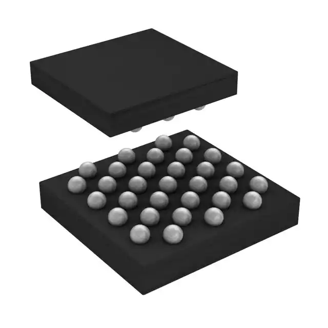
Package Information
Table 2-1.
ATBTLC1000 31L WLCSP Package Information
Parameter
Value
Tolerance
2.262 × 2.142
±0.03
Total thickness
0.502
±0.039
I/O pitch
0.35
Ball diameter
0.2
Ball count
31
Package size
Units
mm
3
±0.03
Block Diagram
Figure 3-1.
ATBTLC1000 Block Diagram
ATBTLC1000 WLCSP SoC [DATASHEET]
Atmel-42493D-ATBTLC1000_WLCSP_SoC-Datasheet_02/2016
5 5
�4
Pinout Information
The ATBTLC1000 is offered in a 0.35mm-pitch staggered SAC405 balls 31L WLCSP package. The WLCSP
package pin assignment is shown in Figure 4-1. The color shading is used to indicate the pin type as follows:
Red – analog
Green – digital I/O (switchable power domain)
Blue – digital I/O (always-on power domain)
Yellow – digital power, purple – PMU
Green/red – configurable mixed-signal GPIO (digital/analog)
The ATBTLC1000 pins are described in Table 4-1.
Figure 4-1.
6
ATBTLC1000 WLCSP Pin Assignment
ATBTLC1000
WLCSP SoC [DATASHEET]
6
Atmel-42493D-ATBTLC1000_WLCSP_SoC-Datasheet_02/2016
�Table 4-1.
ATBTLC1000 WLCSP Pin Description
Pin #
Pin Name
Pin Type
Description / Default Function
A2
VDDIO
Digital Power
I/O Supply, can be less than or equal to VBATT_BUCK
A4
XO_P
Analog/RF
XO Crystal +
A6
VDD_VCO & VDD_SXDIG
Analog/RF
Synthesizer VCO and Digital Supplies 1.2V
B1
AO_GPIO_0
Digital I/O
Always-on External Wakeup
B3
VDDIO_SWITCH
Digital Power
I/O supply switch for external flash
B5
XO_N
Analog/RF
XO Crystal -
B7
RFIO
Analog/RF
RX input and TX output
C2
RTC_CLK_P
PMU
RTC terminal + / 32.768kHz XTAL +
C4
TPP
Analog/RF
Test MUX + output
C6
VDD_RF
Analog/RF
RF Supply 1.2V
D1
RTC_CLK_N
PMU
RTC terminal – / 32.768kHz XTAL -
D3
LP_GPIO_13
Digital I/O
SPI MISO/SPI FLASH RXD
D5
LP_GPIO_0
Digital I/O
SWD Clock
D7
RFGND
Analog/RF
RF Ground
E2
CHIP_EN
PMU
Master Enable for chip
E4
VSS
Digital Power
Digital I/O and Core Ground
E6
VDD_AMS
Analog/RF
AMS Supply 1.2V
F1
LP_LDO_OUT_1P2
PMU
Low Power LDO output (connect to 1µF decoupling cap)
F3
GPIO_MS1
Mixed Signal I/O
Configurable to be a GPIO Mixed Signal only (ADC interface)
F5
LP_GPIO_11
Digital I/O
SPI MOSI/SPI FLASH TXD
F7
LP_GPIO_1
Digital I/O
SWD I/O
G2
VBATT_BUCK
PMU
DC/DC Converter Supply and General Battery Connection
G4
LP_GPIO_12
Digital I/O
SPI SSN/SPI FLASH SSN
G6
LP_GPIO_2
Digital I/O
UART RXD
H1
VDDC_PD4
PMU
DC/DC Converter 1.2V output and feedback node
H3
GND_BUCK
PMU
DC/DC Converter Ground
H5
LP_GPIO_9
Digital I/O
I2C SCL (high-drive pad, see Table 13-3)
H7
LP_GPIO_3
Digital I/O
UART TXD
J2
VSW
PMU
DC/DC Converter Switching Node
J4
LP_GPIO_10
Digital I/O
SPI SCK/SPI FLASH SCK
J6
LP_GPIO_8
Digital I/O
I2C SDA (high-drive pad, see Table 13-3)
ATBTLC1000 WLCSP SoC [DATASHEET]
Atmel-42493D-ATBTLC1000_WLCSP_SoC-Datasheet_02/2016
7 7
�5
Package Drawing
The ATBTLC1000 WLCSP package is RoHS/green compliant.
Figure 5-1.
8
ATBTLC1000 31L WLCSP Package Outline Drawing
ATBTLC1000
WLCSP SoC [DATASHEET]
8
Atmel-42493D-ATBTLC1000_WLCSP_SoC-Datasheet_02/2016
�6
Power Management
6.1
Power Architecture
ATBTLC1000 uses an innovative power architecture to eliminate the need for external regulators and reduce the
number of off-chip components. The integrated power management block includes a DC/DC buck converter and
separate Low Drop out (LDO) regulators for different power domains. The DC/DC buck converter converts battery
voltage to a lower internal voltage for the different circuit blocks and does this with high efficiency. The DC/DC
requires three external components for proper operation (two inductors L 4.7µH and 9.1nH, and one capacitor C
4.7µF).
Figure 6-1.
ATBTLC1000 Power Architecture
RF/AMS
VDD_VCO
LDO2
1.0V
~
SX
VDD_AMS,
VDD_RF,
VDD_SXDIG
RF/AMS Core
VDDIO
Digital
RF/AMS Core Voltage
Pads
Digital Core
eFuse
dcdc_ena
PMU
2.5V
Digital Core Voltage
Sleep
Osc
EFuse
LDO
LP LDO
ena
Dig Core
ena LDO
CHIP_EN
VDDC_PD4
ena
DC/DC Converter
VBATT_BUCK
Vin
Vout
VSW
Off-Chip
LC
ATBTLC1000 WLCSP SoC [DATASHEET]
Atmel-42493D-ATBTLC1000_WLCSP_SoC-Datasheet_02/2016
9 9
�6.2
DC/DC Converter
The DC/DC Converter is intended to supply current to the BLE digital core and the RF transceiver core. The
DC/DC consists of a power switch, 26MHz RC oscillator, controller, external inductor, and external capacitor. The
DC/DC is utilizing pulse skipping discontinuous mode as its control scheme. The DC/DC specifications are shown
in the following tables and figures.
Table 6-1.
DC/DC Converter Specifications (Performance is Guaranteed for (L) 4.7µH and (C) 4.7µF
Parameter
Symbol
Min.
Typ.
Max.
Unit
Note
Output current capability
IREG
0
10
30
mA
Dependent on external component values
and DC/DC settings with acceptable efficiency
External capacitor range
CEXT
4.7
-10%
4.7
20
µF
External capacitance range
External inductor range
LEXT
2.2
-10%
4.7
4.7
+10%
µH
External inductance range
Battery voltage
VBAT
2.35
3
4.3
Functionality and stability given
V
Output voltage range
VREG
Current consumption
IDD
1.05
1.2
tstartup
50
Voltage ripple
ΔVREG
5
85
VOS
0
Line Regulation
ΔVREG
10
Load regulation
ΔVREG
5
Table 6-2.
µA
DC/DC quiescent current
600
µs
Dependent on external component values
and DC/DC settings
30
mV
Dependent on external component values
and DC/DC settings
10
η
Overshoot at startup
25mV step size
125
Startup time
Efficiency
1.47
%
Measured at 3V VBAT, at load of 10mA
No overshoot, no output pre-charge
mV
From 1.8 to 4.3V
From 0 to 10mA
DC/DC Converter Allowable Onboard Inductor and Capacitor Values (VBAT = 3V)
Vripple [mV]
Inductor [µH]
Note:
10
RX Sensitivity (1) [dBm]
Efficiency [%]
C=2.2µF
C=4.7µF
C=10µF
2.2
83
N/A
很抱歉,暂时无法提供与“ATBTLC1000A-UU-T”相匹配的价格&库存,您可以联系我们找货
免费人工找货- 国内价格
- 1+39.62520
- 200+15.81120
- 500+15.28200
- 1500+15.02280