Features
• High-performance, Low-power AVR® 8-bit Microcontroller
• Advanced RISC Architecture
•
•
•
•
•
•
•
– 131 Powerful Instructions – Most Single-clock Cycle Execution
– 32 x 8 General Purpose Working Registers
– Fully Static Operation
– Up to 16 MIPS Throughput at 16 MHz
– On-chip 2-cycle Multiplier
High Endurance Non-volatile Memory segments
– 16K Bytes of In-System Self-programmable Flash program memory
– 512 Bytes EEPROM
– 1K Bytes Internal SRAM
– Write/Erase cycles: 10,000 Flash/100,000 EEPROM
– Data retention: 20 years at 85°C/100 years at 25°C(1)
– Optional Boot Code Section with Independent Lock Bits
In-System Programming by On-chip Boot Program
True Read-While-Write Operation
– Up to 64K Bytes Optional External Memory Space
– Programming Lock for Software Security
JTAG (IEEE std. 1149.1 Compliant) Interface
– Boundary-scan Capabilities According to the JTAG Standard
– Extensive On-chip Debug Support
– Programming of Flash, EEPROM, Fuses, and Lock Bits through the JTAG Interface
Peripheral Features
– Two 8-bit Timer/Counters with Separate Prescalers and Compare Modes
– Two 16-bit Timer/Counters with Separate Prescalers, Compare Modes, and
Capture Modes
– Real Time Counter with Separate Oscillator
– Six PWM Channels
– Dual Programmable Serial USARTs
– Master/Slave SPI Serial Interface
– Programmable Watchdog Timer with Separate On-chip Oscillator
– On-chip Analog Comparator
Special Microcontroller Features
– Power-on Reset and Programmable Brown-out Detection
– Internal Calibrated RC Oscillator
– External and Internal Interrupt Sources
– Five Sleep Modes: Idle, Power-save, Power-down, Standby, and Extended Standby
I/O and Packages
– 35 Programmable I/O Lines
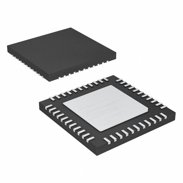
– 40-pin PDIP, 44-lead TQFP, and 44-pad MLF
Operating Voltages
– 1.8 - 5.5V for ATmega162V
– 2.7 - 5.5V for ATmega162
Speed Grades
– 0 - 8 MHz for ATmega162V (see Figure 113 on page 266)
– 0 - 16 MHz for ATmega162 (see Figure 114 on page 266)
8-bit
Microcontroller
with 16K Bytes
In-System
Programmable
Flash
ATmega162
ATmega162V
Summary
2513LS–AVR–03/2013
�Pin
Configurations
Figure 1. Pinout ATmega162
PDIP
(OC0/T0) PB0
(OC2/T1) PB1
(RXD1/AIN0) PB2
(TXD1/AIN1) PB3
(SS/OC3B) PB4
(MOSI) PB5
(MISO) PB6
(SCK) PB7
RESET
(RXD0) PD0
(TXD0) PD1
(INT0/XCK1) PD2
(INT1/ICP3) PD3
(TOSC1/XCK0/OC3A) PD4
(OC1A/TOSC2) PD5
(WR) PD6
(RD) PD7
XTAL2
XTAL1
GND
1
2
3
4
5
6
7
8
9
10
11
12
13
14
15
16
17
18
19
20
40
39
38
37
36
35
34
33
32
31
30
29
28
27
26
25
24
23
22
21
VCC
PA0 (AD0/PCINT0)
PA1 (AD1/PCINT1)
PA2 (AD2/PCINT2)
PA3 (AD3/PCINT3)
PA4 (AD4/PCINT4)
PA5 (AD5/PCINT5)
PA6 (AD6/PCINT6)
PA7 (AD7/PCINT7)
PE0 (ICP1/INT2)
PE1 (ALE)
PE2 (OC1B)
PC7 (A15/TDI/PCINT15)
PC6 (A14/TDO/PCINT14)
PC5 (A13/TMS/PCINT13)
PC4 (A12/TCK/PCINT12)
PC3 (A11/PCINT11)
PC2 (A10/PCINT10)
PC1 (A9/PCINT9)
PC0 (A8/PCINT8)
PB4 (SS/OC3B)
PB3 (TXD1/AIN1)
PB2 (RXD1/AIN0)
PB1 (OC2/T1)
PB0 (OC0/T0)
GND
VCC
PA0 (AD0/PCINT0)
PA1 (AD1/PCINT1)
PA2 (AD2/PCINT2)
PA3 (AD3/PCINT3)
TQFP/MLF
NOTE:
MLF bottom pad should
be soldered to ground.
Disclaimer
2
44 42 40 38 36 34
43 41 39 37 35
33
1
32
2
31
3
30
4
29
5
28
6
27
7
26
8
25
9
24
10
23
11
13 15 17 19 21
12 14 16 18 20 22
PA4 (AD4/PCINT4)
PA5 (AD5/PCINT5)
PA6 (AD6/PCINT6)
PA7 (AD7/PCINT7)
PE0 (ICP1/INT2)
GND
PE1 (ALE)
PE2 (OC1B)
PC7 (A15/TDI/PCINT15)
PC6 (A14/TDO/PCINT14)
PC5 (A13/TMS/PCINT13)
(WR) PD6
(RD) PD7
XTAL2
XTAL1
GND
VCC
(A8/PCINT8) PC0
(A9/PCINT9) PC1
(A10/PCINT10) PC2
(A11/PCINT11) PC3
(TCK/A12/PCINT12) PC4
(MOSI) PB5
(MISO) PB6
(SCK) PB7
RESET
(RXD0) PD0
VCC
(TXD0) PD1
(INT0/XCK1) PD2
(INT1/ICP3) PD3
(TOSC1/XCK0/OC3A) PD4
(OC1A/TOSC2) PD5
Typical values contained in this datasheet are based on simulations and characterization of
other AVR microcontrollers manufactured on the same process technology. Min and Max values
will be available after the device is characterized.
ATmega162/V
2513LS–AVR–03/2013
�ATmega162/V
Overview
The ATmega162 is a low-power CMOS 8-bit microcontroller based on the AVR enhanced RISC
architecture. By executing powerful instructions in a single clock cycle, the ATmega162
achieves throughputs approaching 1 MIPS per MHz allowing the system designer to optimize
power consumption versus processing speed.
Block Diagram
Figure 2. Block Diagram
PA0 - PA7
PE0 - PE2
PC0 - PC7
PORTA DRIVERS/BUFFERS
PORTE
DRIVERS/
BUFFERS
PORTC DRIVERS/BUFFERS
PORTA DIGITAL INTERFACE
PORTE
DIGITAL
INTERFACE
PORTC DIGITAL INTERFACE
VCC
GND
PROGRAM
COUNTER
STACK
POINTER
INTERNAL
OSCILLATOR
XTAL1
PROGRAM
FLASH
SRAM
WATCHDOG
TIMER
OSCILLATOR
XTAL2
INSTRUCTION
REGISTER
GENERAL
PURPOSE
REGISTERS
MCU CTRL.
& TIMING
X
INSTRUCTION
DECODER
Y
INTERRUPT
UNIT
INTERNAL
CALIBRATED
OSCILLATOR
TIMERS/
COUNTERS
OSCILLATOR
Z
CONTROL
LINES
ALU
AVR CPU
STATUS
REGISTER
EEPROM
PROGRAMMING
LOGIC
SPI
USART0
COMP.
INTERFACE
USART1
+
-
RESET
PORTB DIGITAL INTERFACE
PORTD DIGITAL INTERFACE
PORTB DRIVERS/BUFFERS
PORTD DRIVERS/BUFFERS
PB0 - PB7
PD0 - PD7
3
2513LS–AVR–03/2013
�The AVR core combines a rich instruction set with 32 general purpose working registers. All the
32 registers are directly connected to the Arithmetic Logic Unit (ALU), allowing two independent
registers to be accessed in one single instruction executed in one clock cycle. The resulting
architecture is more code efficient while achieving throughputs up to ten times faster than conventional CISC microcontrollers.
The ATmega162 provides the following features: 16K bytes of In-System Programmable Flash
with Read-While-Write capabilities, 512 bytes EEPROM, 1K bytes SRAM, an external memory
interface, 35 general purpose I/O lines, 32 general purpose working registers, a JTAG interface
for Boundary-scan, On-chip Debugging support and programming, four flexible Timer/Counters
with compare modes, internal and external interrupts, two serial programmable USARTs, a programmable Watchdog Timer with Internal Oscillator, an SPI serial port, and five software
selectable power saving modes. The Idle mode stops the CPU while allowing the SRAM,
Timer/Counters, SPI port, and interrupt system to continue functioning. The Power-down mode
saves the register contents but freezes the Oscillator, disabling all other chip functions until the
next interrupt or Hardware Reset. In Power-save mode, the Asynchronous Timer continues to
run, allowing the user to maintain a timer base while the rest of the device is sleeping. In
Standby mode, the crystal/resonator Oscillator is running while the rest of the device is sleeping.
This allows very fast start-up combined with low-power consumption. In Extended Standby
mode, both the main Oscillator and the Asynchronous Timer continue to run.
The device is manufactured using Atmel’s high density non-volatile memory technology. The
On-chip ISP Flash allows the program memory to be reprogrammed In-System through an SPI
serial interface, by a conventional non-volatile memory programmer, or by an On-chip Boot Program running on the AVR core. The Boot Program can use any interface to download the
Application Program in the Application Flash memory. Software in the Boot Flash section will
continue to run while the Application Flash section is updated, providing true Read-While-Write
operation. By combining an 8-bit RISC CPU with In-System Self-Programmable Flash on a
monolithic chip, the Atmel ATmega162 is a powerful microcontroller that provides a highly flexible and cost effective solution to many embedded control applications.
The ATmega162 AVR is supported with a full suite of program and system development tools
including: C compilers, macro assemblers, program debugger/simulators, In-Circuit Emulators,
and evaluation kits.
ATmega161 and
ATmega162
Compatibility
The ATmega162 is a highly complex microcontroller where the number of I/O locations supersedes the 64 I/O locations reserved in the AVR instruction set. To ensure back-ward
compatibility with the ATmega161, all I/O locations present in ATmega161 have the same locations in ATmega162. Some additional I/O locations are added in an Extended I/O space starting
from 0x60 to 0xFF, (i.e., in the ATmega162 internal RAM space). These locations can be
reached by using LD/LDS/LDD and ST/STS/STD instructions only, not by using IN and OUT
instructions. The relocation of the internal RAM space may still be a problem for ATmega161
users. Also, the increased number of Interrupt Vectors might be a problem if the code uses
absolute addresses. To solve these problems, an ATmega161 compatibility mode can be
selected by programming the fuse M161C. In this mode, none of the functions in the Extended
I/O space are in use, so the internal RAM is located as in ATmega161. Also, the Extended Interrupt Vec-tors are removed. The ATmega162 is 100% pin compatible with ATmega161, and can
replace the ATmega161 on current Printed Circuit Boards. However, the location of Fuse bits
and the electrical characteristics differs between the two devices.
ATmega161
Compatibility Mode
Programming the M161C will change the following functionality:
4
•
The extended I/O map will be configured as internal RAM once the M161C Fuse is
programmed.
ATmega162/V
2513LS–AVR–03/2013
�ATmega162/V
•
The timed sequence for changing the Watchdog Time-out period is disabled. See “Timed
Sequences for Changing the Configuration of the Watchdog Timer” on page 56 for details.
•
The double buffering of the USART Receive Registers is disabled. See “AVR USART vs.
AVR UART – Compatibility” on page 168 for details.
•
Pin change interrupts are not supported (Control Registers are located in Extended I/O).
•
One 16 bits Timer/Counter (Timer/Counter1) only. Timer/Counter3 is not accessible.
Note that the shared UBRRHI Register in ATmega161 is split into two separate registers in
ATmega162, UBRR0H and UBRR1H. The location of these registers will not be affected by the
ATmega161 compatibility fuse.
Pin Descriptions
VCC
Digital supply voltage
GND
Ground
Port A (PA7..PA0)
Port A is an 8-bit bi-directional I/O port with internal pull-up resistors (selected for each bit). The
Port A output buffers have symmetrical drive characteristics with both high sink and source
capability. When pins PA0 to PA7 are used as inputs and are externally pulled low, they will
source current if the internal pull-up resistors are activated. The Port A pins are tri-stated when a
reset condition becomes active, even if the clock is not running.
Port A also serves the functions of various special features of the ATmega162 as listed on page
72.
Port B (PB7..PB0)
Port B is an 8-bit bi-directional I/O port with internal pull-up resistors (selected for each bit). The
Port B output buffers have symmetrical drive characteristics with both high sink and source
capability. As inputs, Port B pins that are externally pulled low will source current if the pull-up
resistors are activated. The Port B pins are tri-stated when a reset condition becomes active,
even if the clock is not running.
Port B also serves the functions of various special features of the ATmega162 as listed on page
72.
Port C (PC7..PC0)
Port C is an 8-bit bi-directional I/O port with internal pull-up resistors (selected for each bit). The
Port C output buffers have symmetrical drive characteristics with both high sink and source
capability. As inputs, Port C pins that are externally pulled low will source current if the pull-up
resistors are activated. The Port C pins are tri-stated when a reset condition becomes active,
even if the clock is not running. If the JTAG interface is enabled, the pull-up resistors on pins
PC7(TDI), PC5(TMS) and PC4(TCK) will be activated even if a Reset occurs.
Port C also serves the functions of the JTAG interface and other special features of the
ATmega162 as listed on page 75.
5
2513LS–AVR–03/2013
�Port D (PD7..PD0)
Port D is an 8-bit bi-directional I/O port with internal pull-up resistors (selected for each bit). The
Port D output buffers have symmetrical drive characteristics with both high sink and source
capability. As inputs, Port D pins that are externally pulled low will source current if the pull-up
resistors are activated. The Port D pins are tri-stated when a reset condition becomes active,
even if the clock is not running.
Port D also serves the functions of various special features of the ATmega162 as listed on page
78.
Port E(PE2..PE0)
Port E is an 3-bit bi-directional I/O port with internal pull-up resistors (selected for each bit). The
Port E output buffers have symmetrical drive characteristics with both high sink and source
capability. As inputs, Port E pins that are externally pulled low will source current if the pull-up
resistors are activated. The Port E pins are tri-stated when a reset condition becomes active,
even if the clock is not running.
Port E also serves the functions of various special features of the ATmega162 as listed on page
81.
RESET
Reset input. A low level on this pin for longer than the minimum pulse length will generate a
Reset, even if the clock is not running. The minimum pulse length is given in Table 18 on page
48. Shorter pulses are not guaranteed to generate a reset.
XTAL1
Input to the Inverting Oscillator amplifier and input to the internal clock operating circuit.
XTAL2
Output from the Inverting Oscillator amplifier.
6
ATmega162/V
2513LS–AVR–03/2013
�ATmega162/V
Resources
A comprehensive set of development tools, application notes and datasheets are available for
download on http://www.atmel.com/avr.
Note:
Data Retention
1.
Reliability Qualification results show that the projected data retention failure rate is much less
than 1 PPM over 20 years at 85°C or 100 years at 25°C.
7
2513LS–AVR–03/2013
�Register Summary
8
Address
Name
Bit 7
Bit 6
Bit 5
Bit 4
Bit 3
Bit 2
Bit 1
Bit 0
(0xFF)
Reserved
–
–
–
–
–
–
–
–
..
Reserved
–
–
–
–
–
–
–
–
(0x9E)
Reserved
–
–
–
–
–
–
–
–
(0x9D)
Reserved
–
–
–
–
–
–
–
–
(0x9C)
Reserved
–
–
–
–
–
–
–
–
(0x9B)
Reserved
–
–
–
–
–
–
–
–
(0x9A)
Reserved
–
–
–
–
–
–
–
–
(0x99)
Reserved
–
–
–
–
–
–
–
–
(0x98)
Reserved
–
–
–
–
–
–
–
–
(0x97)
Reserved
–
–
–
–
–
–
–
–
(0x96)
Reserved
–
–
–
–
–
–
–
–
(0x95)
Reserved
–
–
–
–
–
–
–
–
(0x94)
Reserved
–
–
–
–
–
–
–
–
(0x93)
Reserved
–
–
–
–
–
–
–
–
(0x92)
Reserved
–
–
–
–
–
–
–
–
(0x91)
Reserved
–
–
–
–
–
–
–
–
(0x90)
Reserved
–
–
–
–
–
–
–
–
(0x8F)
Reserved
–
–
–
–
–
–
–
–
(0x8E)
Reserved
–
–
–
–
–
–
–
–
(0x8D)
Reserved
–
–
–
–
–
–
–
–
(0x8C)
Reserved
–
–
–
–
–
–
–
–
(0x8B)
TCCR3A
COM3A1
COM3A0
COM3B1
COM3B0
FOC3A
FOC3B
WGM31
WGM30
(0x8A)
TCCR3B
ICNC3
ICES3
–
WGM33
WGM32
CS32
CS31
CS30
(0x89)
TCNT3H
Page
131
128
Timer/Counter3 – Counter Register High Byte
133
133
(0x88)
TCNT3L
Timer/Counter3 – Counter Register Low Byte
(0x87)
OCR3AH
Timer/Counter3 – Output Compare Register A High Byte
133
(0x86)
OCR3AL
Timer/Counter3 – Output Compare Register A Low Byte
133
(0x85)
OCR3BH
Timer/Counter3 – Output Compare Register B High Byte
133
(0x84)
OCR3BL
Timer/Counter3 – Output Compare Register B Low Byte
133
(0x83)
Reserved
–
–
–
–
–
–
–
–
(0x82)
Reserved
–
–
–
–
–
–
–
–
(0x81)
ICR3H
Timer/Counter3 – Input Capture Register High Byte
(0x80)
ICR3L
Timer/Counter3 – Input Capture Register Low Byte
(0x7F)
Reserved
–
–
–
–
–
134
134
–
–
–
(0x7E)
Reserved
–
–
–
–
–
–
–
–
(0x7D)
ETIMSK
–
–
TICIE3
OCIE3A
OCIE3B
TOIE3
–
–
135
(0x7C)
ETIFR
–
–
ICF3
OCF3A
OCF3B
TOV3
–
–
135
(0x7B)
Reserved
–
–
–
–
–
–
–
–
(0x7A)
Reserved
–
–
–
–
–
–
–
–
(0x79)
Reserved
–
–
–
–
–
–
–
–
(0x78)
Reserved
–
–
–
–
–
–
–
–
(0x77)
Reserved
–
–
–
–
–
–
–
–
(0x76)
Reserved
–
–
–
–
–
–
–
–
(0x75)
Reserved
–
–
–
–
–
–
–
–
(0x74)
Reserved
–
–
–
–
–
–
–
–
(0x73)
Reserved
–
–
–
–
–
–
–
–
(0x72)
Reserved
–
–
–
–
–
–
–
–
(0x71)
Reserved
–
–
–
–
–
–
–
–
(0x70)
Reserved
–
–
–
–
–
–
–
–
(0x6F)
Reserved
–
–
–
–
–
–
–
–
(0x6E)
Reserved
–
–
–
–
–
–
–
–
(0x6D)
Reserved
–
–
–
–
–
–
–
–
(0x6C)
PCMSK1
PCINT15
PCINT14
PCINT13
PCINT12
PCINT11
PCINT10
PCINT9
PCINT8
88
(0x6B)
PCMSK0
PCINT7
PCINT6
PCINT5
PCINT4
PCINT3
PCINT2
PCINT1
PCINT0
88
(0x6A)
Reserved
–
–
–
–
–
–
–
–
(0x69)
Reserved
–
–
–
–
–
–
–
–
(0x68)
Reserved
–
–
–
–
–
–
–
–
(0x67)
Reserved
–
–
–
–
–
–
–
–
(0x66)
Reserved
–
–
–
–
–
–
–
–
(0x65)
Reserved
–
–
–
–
–
–
–
–
(0x64)
Reserved
–
–
–
–
–
–
–
–
(0x63)
Reserved
–
–
–
–
–
–
–
–
(0x62)
Reserved
–
–
–
–
–
–
–
–
(0x61)
CLKPR
CLKPCE
–
–
–
CLKPS3
CLKPS2
CLKPS1
CLKPS0
41
ATmega162/V
2513LS–AVR–03/2013
�ATmega162/V
Address
Name
Bit 7
Bit 6
Bit 5
Bit 4
Bit 3
Bit 2
Bit 1
Bit 0
(0x60)
Reserved
–
–
–
–
–
–
–
–
0x3F (0x5F)
SREG
I
T
H
S
V
N
Z
C
10
0x3E (0x5E)
SPH
SP15
SP14
SP13
SP12
SP11
SP10
SP9
SP8
13
SP6
SP5
SP4
SP3
SP2
SP1
UBRR1[11:8]
SP0
0x3D (0x5D)
(2)
(2)
0x3C (0x5C)
0x3B (0x5B)
Page
SPL
SP7
UBRR1H
URSEL1
13
UCSR1C
URSEL1
UMSEL1
UPM11
UPM10
USBS1
UCSZ11
UCSZ10
UCPOL1
189
GICR
INT1
INT0
INT2
PCIE1
PCIE0
–
IVSEL
IVCE
61, 86
190
0x3A (0x5A)
GIFR
INTF1
INTF0
INTF2
PCIF1
PCIF0
–
–
–
87
0x39 (0x59)
TIMSK
TOIE1
OCIE1A
OCIE1B
OCIE2
TICIE1
TOIE2
TOIE0
OCIE0
102, 134, 154
103, 135, 155
0x38 (0x58)
TIFR
TOV1
OCF1A
OCF1B
OCF2
ICF1
TOV2
TOV0
OCF0
0x37 (0x57)
SPMCR
SPMIE
RWWSB
–
RWWSRE
BLBSET
PGWRT
PGERS
SPMEN
221
0x36 (0x56)
EMCUCR
SM0
SRL2
SRL1
SRL0
SRW01
SRW00
SRW11
ISC2
30,44,85
0x35 (0x55)
MCUCR
SRE
SRW10
SE
SM1
ISC11
ISC10
ISC01
ISC00
30,43,84
0x34 (0x54)
MCUCSR
JTD
–
SM2
JTRF
WDRF
BORF
EXTRF
PORF
43,51,207
0x33 (0x53)
TCCR0
FOC0
WGM00
COM01
COM00
WGM01
CS02
CS01
CS00
0x32 (0x52)
0x31 (0x51)
TCNT0
0x30 (0x50)
SFIOR
TSM
XMBK
XMM2
XMM1
Timer/Counter0 (8 Bits)
OCR0
100
102
Timer/Counter0 Output Compare Register
102
XMM0
PUD
PSR2
PSR310
32,70,105,156
128
0x2F (0x4F)
TCCR1A
COM1A1
COM1A0
COM1B1
COM1B0
FOC1A
FOC1B
WGM11
WGM10
0x2E (0x4E)
TCCR1B
ICNC1
ICES1
–
WGM13
WGM12
CS12
CS11
CS10
0x2D (0x4D)
TCNT1H
Timer/Counter1 – Counter Register High Byte
131
133
0x2C (0x4C)
TCNT1L
Timer/Counter1 – Counter Register Low Byte
133
0x2B (0x4B)
OCR1AH
Timer/Counter1 – Output Compare Register A High Byte
133
0x2A (0x4A)
OCR1AL
Timer/Counter1 – Output Compare Register A Low Byte
133
0x29 (0x49)
OCR1BH
Timer/Counter1 – Output Compare Register B High Byte
133
0x28 (0x48)
OCR1BL
0x27 (0x47)
TCCR2
FOC2
WGM20
COM21
COM20
WGM21
CS22
CS21
CS20
149
–
–
–
–
AS2
TCN2UB
OCR2UB
TCR2UB
152
Timer/Counter1 – Output Compare Register B Low Byte
133
0x26 (0x46)
ASSR
0x25 (0x45)
ICR1H
Timer/Counter1 – Input Capture Register High Byte
0x24 (0x44)
ICR1L
Timer/Counter1 – Input Capture Register Low Byte
134
0x23 (0x43)
TCNT2
Timer/Counter2 (8 Bits)
151
0x22 (0x42)
OCR2
0x21 (0x41)
WDTCR
–
–
–
WDCE
UBRR0H
URSEL0
–
–
–
(2)
0x20
(0x40)
(2)
134
Timer/Counter2 Output Compare Register
WDE
151
WDP2
WDP1
WDP0
UBRR0[11:8]
53
190
UCSR0C
URSEL0
UMSEL0
UPM01
UPM00
USBS0
UCSZ01
UCSZ00
UCPOL0
189
0x1F (0x3F)
EEARH
–
–
–
–
–
–
–
EEAR8
20
0x1E (0x3E)
EEARL
EEPROM Address Register Low Byte
20
0x1D (0x3D)
EEDR
EEPROM Data Register
21
0x1C (0x3C)
EECR
–
–
–
–
EERIE
EEMWE
EEWE
EERE
0x1B (0x3B)
PORTA
PORTA7
PORTA6
PORTA5
PORTA4
PORTA3
PORTA2
PORTA1
PORTA0
21
82
0x1A (0x3A)
DDRA
DDA7
DDA6
DDA5
DDA4
DDA3
DDA2
DDA1
DDA0
82
0x19 (0x39)
PINA
PINA7
PINA6
PINA5
PINA4
PINA3
PINA2
PINA1
PINA0
82
0x18 (0x38)
PORTB
PORTB7
PORTB6
PORTB5
PORTB4
PORTB3
PORTB2
PORTB1
PORTB0
82
0x17 (0x37)
DDRB
DDB7
DDB6
DDB5
DDB4
DDB3
DDB2
DDB1
DDB0
82
0x16 (0x36)
PINB
PINB7
PINB6
PINB5
PINB4
PINB3
PINB2
PINB1
PINB0
82
0x15 (0x35)
PORTC
PORTC7
PORTC6
PORTC5
PORTC4
PORTC3
PORTC2
PORTC1
PORTC0
82
0x14 (0x34)
DDRC
DDC7
DDC6
DDC5
DDC4
DDC3
DDC2
DDC1
DDC0
82
0x13 (0x33)
PINC
PINC7
PINC6
PINC5
PINC4
PINC3
PINC2
PINC1
PINC0
83
0x12 (0x32)
PORTD
PORTD7
PORTD6
PORTD5
PORTD4
PORTD3
PORTD2
PORTD1
PORTD0
83
0x11 (0x31)
DDRD
DDD7
DDD6
DDD5
DDD4
DDD3
DDD2
DDD1
DDD0
83
0x10 (0x30)
PIND
PIND7
PIND6
PIND5
PIND4
PIND3
PIND2
PIND1
PIND0
0x0F (0x2F)
SPDR
SPI Data Register
83
164
0x0E (0x2E)
SPSR
SPIF
WCOL
–
–
–
–
–
SPI2X
164
0x0D (0x2D)
SPCR
SPIE
SPE
DORD
MSTR
CPOL
CPHA
SPR1
SPR0
162
0x0C (0x2C)
UDR0
0x0B (0x2B)
UCSR0A
RXC0
TXC0
UDRE0
186
0x0A (0x2A)
UCSR0B
RXCIE0
TXCIE0
UDRIE0
0x09 (0x29)
UBRR0L
USART0 I/O Data Register
186
FE0
DOR0
UPE0
U2X0
MPCM0
RXEN0
TXEN0
UCSZ02
RXB80
TXB80
USART0 Baud Rate Register Low Byte
187
190
0x08 (0x28)
ACSR
ACD
ACBG
ACO
ACI
ACIE
ACIC
ACIS1
ACIS0
0x07 (0x27)
PORTE
–
–
–
–
–
PORTE2
PORTE1
PORTE0
83
0x06 (0x26)
DDRE
–
–
–
–
–
DDE2
DDE1
DDE0
83
PINE
–
–
–
–
–
PINE2
PINE1
PINE0
83
OSCCAL
–
CAL6
CAL5
CAL4
CAL3
CAL2
CAL1
CAL0
39
0x05 (0x25)
0x04(1) (0x24)(1)
OCDR
On-chip Debug Register
0x03 (0x23)
UDR1
USART1 I/O Data Register
0x02 (0x22)
UCSR1A
RXC1
TXC1
UDRE1
FE1
DOR1
195
202
186
UPE1
U2X1
MPCM1
186
9
2513LS–AVR–03/2013
�Address
Name
Bit 7
Bit 6
Bit 5
Bit 4
Bit 3
Bit 2
Bit 1
Bit 0
Page
0x01 (0x21)
UCSR1B
RXCIE1
TXCIE1
UDRIE1
RXEN1
TXEN1
UCSZ12
RXB81
TXB81
187
0x00 (0x20)
UBRR1L
Notes:
10
USART1 Baud Rate Register Low Byte
190
1. When the OCDEN Fuse is unprogrammed, the OSCCAL Register is always accessed on this address. Refer to the debugger specific documentation for details on how to use the OCDR Register.
2. Refer to the USART description for details on how to access UBRRH and UCSRC.
3. For compatibility with future devices, reserved bits should be written to zero if accessed. Reserved I/O memory addresses
should never be written.
4. Some of the Status Flags are cleared by writing a logical one to them. Note that the CBI and SBI instructions will operate on
all bits in the I/O Register, writing a one back into any flag read as set, thus clearing the flag. The CBI and SBI instructions
work with registers 0x00 to 0x1F only.
ATmega162/V
2513LS–AVR–03/2013
�ATmega162/V
Instruction Set Summary
Mnemonics
Operands
Description
Operation
Flags
#Clocks
ARITHMETIC AND LOGIC INSTRUCTIONS
ADD
Rd, Rr
Add two Registers
Rd Rd + Rr
Z,C,N,V,H
ADC
Rd, Rr
Add with Carry two Registers
Rd Rd + Rr + C
Z,C,N,V,H
1
ADIW
Rdl,K
Add Immediate to Word
Rdh:Rdl Rdh:Rdl + K
Z,C,N,V,S
2
SUB
Rd, Rr
Subtract two Registers
Rd Rd - Rr
Z,C,N,V,H
1
SUBI
Rd, K
Subtract Constant from Register
Rd Rd - K
Z,C,N,V,H
1
SBC
Rd, Rr
Subtract with Carry two Registers
Rd Rd - Rr - C
Z,C,N,V,H
1
1
SBCI
Rd, K
Subtract with Carry Constant from Reg.
Rd Rd - K - C
Z,C,N,V,H
1
SBIW
Rdl,K
Subtract Immediate from Word
Rdh:Rdl Rdh:Rdl - K
Z,C,N,V,S
2
1
AND
Rd, Rr
Logical AND Registers
Rd Rd Rr
Z,N,V
ANDI
Rd, K
Logical AND Register and Constant
Rd Rd K
Z,N,V
1
OR
Rd, Rr
Logical OR Registers
Rd Rd v Rr
Z,N,V
1
ORI
Rd, K
Logical OR Register and Constant
Rd Rd v K
Z,N,V
1
EOR
Rd, Rr
Exclusive OR Registers
Rd Rd Rr
Z,N,V
1
COM
Rd
One’s Complement
Rd 0xFF Rd
Z,C,N,V
1
NEG
Rd
Two’s Complement
Rd 0x00 Rd
Z,C,N,V,H
1
SBR
Rd,K
Set Bit(s) in Register
Rd Rd v K
Z,N,V
1
CBR
Rd,K
Clear Bit(s) in Register
Rd Rd (0xFF - K)
Z,N,V
1
INC
Rd
Increment
Rd Rd + 1
Z,N,V
1
DEC
Rd
Decrement
Rd Rd 1
Z,N,V
1
TST
Rd
Test for Zero or Minus
Rd Rd Rd
Z,N,V
1
CLR
Rd
Clear Register
Rd Rd Rd
Z,N,V
1
SER
Rd
Set Register
Rd 0xFF
None
1
MUL
Rd, Rr
Multiply Unsigned
R1:R0 Rd x Rr
Z,C
2
MULS
Rd, Rr
Multiply Signed
R1:R0 Rd x Rr
Z,C
2
MULSU
Rd, Rr
Multiply Signed with Unsigned
R1:R0 Rd x Rr
Z,C
2
FMUL
Rd, Rr
Fractional Multiply Unsigned
R1:R0 (Rd x Rr)


 工商网监
湘ICP备2023018690号
工商网监
湘ICP备2023018690号
