This is a summary document. A
complete document is available on
our Web site at www.microchip.com
ATmega328PB
ATmega328PB Summary Datasheet
Introduction
®
The picoPower ATmega328PB is a low-power CMOS 8-bit microcontroller based on the AVR® enhanced
RISC architecture. By executing powerful instructions in a single clock cycle, the ATmega328PB achieves
throughputs close to 1MIPS per MHz. This empowers system designers to optimize the device for power
consumption versus processing speed.
Features
High Performance, Low Power AVR® 8-Bit Microcontroller Family
•
Advanced RISC Architecture
– 131 Powerful Instructions
– Most Single Clock Cycle Execution
– 32 x 8 General Purpose Working Registers
– Fully Static Operation
– Up to 20 MIPS Throughput at 20MHz
– On-Chip 2-Cycle Multiplier
•
High Endurance Non-Volatile Memory Segments
– 32KBytes of In-System Self-Programmable Flash program memory
– 1KBytes EEPROM
– 2KBytes Internal SRAM
– Write/Erase Cycles: 10,000 Flash/100,000 EEPROM
– Data retention: 20 years at 85°C
– Optional Boot Code Section with Independent Lock Bits
• In-System Programming by On-chip Boot Program
• True Read-While-Write Operation
– Programming Lock for Software Security
•
Peripheral Features
– Peripheral Touch Controller (PTC)
• Capacitive Touch Buttons, Sliders and Wheels
• 24 Self-Cap Channels and 144 Mutual Cap Channels
– Two 8-bit Timer/Counters with Separate Prescaler and Compare Mode
– Three 16-bit Timer/Counters with Separate Prescaler, Compare Mode, and Capture Mode
– Real Time Counter with Separate Oscillator
– Ten PWM Channels
– 8-channel 10-bit ADC in TQFP and QFN/MLF package
– Two Programmable Serial USARTs
© 2017 Microchip Technology Inc.
Datasheet Summary
40001907A-page 1
�ATmega328PB
•
– Two Master/Slave SPI Serial Interfaces
– Two Byte-Oriented 2-Wire Serial Interfaces (Philips I2C Compatible)
– Programmable Watchdog Timer with Separate On-chip Oscillator
– On-Chip Analog Comparator
– Interrupt and Wake-Up on Pin Change
Special Microcontroller Features
– Power-On Reset and Programmable Brown-Out Detection
– Internal 8 MHz Calibrated Oscillator
–
–
•
•
•
•
•
External and Internal Interrupt Sources
Six Sleep Modes: Idle, ADC Noise Reduction, Power-save, Power-down, Standby, and Extended
Standby
– Clock Failure Detection Mechanism and Switch to Internal 8 MHz RC Oscillator in case of Failure
– Individual Serial Number to Represent a Unique ID
I/O and Packages
– 27 Programmable I/O Lines
– 32-pin TQFP and 32-pin QFN/MLF
Operating Voltage:
– 1.8 - 5.5V
Temperature Range:
– -40°C to 105°C
Speed Grade:
– 0 - 4MHz @ 1.8 - 5.5V
– 0 - 10MHz @ 2.7 - 5.5.V
– 0 - 20MHz @ 4.5 - 5.5V
Power Consumption at 1MHz, 1.8V, 25°C
– Active Mode: 0.24mA
– Power-Down Mode: 0.2μA
– Power-Save Mode: 1.3μA (Including 32kHz RTC)
© 2017 Microchip Technology Inc.
Datasheet Summary
40001907A-page 2
�Table of Contents
Introduction......................................................................................................................1
Features.......................................................................................................................... 1
1. Description.................................................................................................................4
2. Configuration Summary.............................................................................................5
3. Ordering Information..................................................................................................6
4. Block Diagram........................................................................................................... 7
5. Pin Configurations..................................................................................................... 8
5.1.
Pin Descriptions........................................................................................................................... 9
6. I/O Multiplexing........................................................................................................ 11
7. Resources............................................................................................................... 12
8. About Code Examples.............................................................................................13
The Microchip Web Site................................................................................................ 14
Customer Change Notification Service..........................................................................14
Customer Support......................................................................................................... 14
Microchip Devices Code Protection Feature................................................................. 14
Legal Notice...................................................................................................................15
Trademarks................................................................................................................... 15
Quality Management System Certified by DNV.............................................................16
Worldwide Sales and Service........................................................................................17
© 2017 Microchip Technology Inc.
Datasheet Summary
40001907A-page 3
�ATmega328PB
1.
Description
The ATmega328PB is a low-power CMOS 8-bit microcontroller based on the AVR enhanced RISC
architecture. By executing powerful instructions in a single clock cycle, the ATmega328PB achieves
throughputs close to 1MIPS per MHz. This empowers system designer to optimize the device for power
consumption versus processing speed.
The core combines a rich instruction set with 32 general purpose working registers. All the 32 registers
are directly connected to the Arithmetic Logic Unit (ALU), allowing two independent registers to be
accessed in a single instruction executed in one clock cycle. The resulting architecture is more code
efficient while achieving throughputs up to ten times faster than conventional CISC microcontrollers.
The ATmega328PB provides the following features: 32Kbytes of In-System Programmable Flash with
Read-While-Write capabilities, 1Kbytes EEPROM, 2Kbytes SRAM, 27 general purpose I/O lines, 32
general purpose working registers, five flexible Timer/Counters with compare modes, internal and
external interrupts, two serial programmable USART, two byte-oriented 2-wire Serial Interface (I2C), two
SPI serial ports, a 8-channel 10-bit ADC in TQFP and QFN/MLF package, a programmable Watchdog
Timer with internal Oscillator, Clock failure detection mechanism and six software selectable power
saving modes. The Idle mode stops the CPU while allowing the SRAM, Timer/Counters, USART, 2-wire
Serial Interface, SPI port, and interrupt system to continue functioning. PTC with enabling up to 24 selfcap and 144 mutual-cap sensors. The Power-down mode saves the register contents but freezes the
Oscillator, disabling all other chip functions until the next interrupt or hardware reset. In Power-save
mode, the asynchronous timer continues to run, allowing the user to maintain a timer base while the rest
of the device is sleeping. Also ability to run PTC in power-save mode/wake-up on touch and Dynamic
on/off of PTC analog and digital portion. The ADC Noise Reduction mode stops the CPU and all I/O
modules except asynchronous timer, PTC, and ADC to minimize switching noise during ADC
conversions. In Standby mode, the crystal/resonator Oscillator is running while the rest of the device is
sleeping. This allows very fast start-up combined with low power consumption.
The device is manufactured using high density non-volatile memory technology. The On-chip ISP Flash
allows the program memory to be reprogrammed In-System through an SPI serial interface, by a
conventional nonvolatile memory programmer, or by an On-chip Boot program running on the AVR core.
The Boot program can use any interface to download the application program in the Application Flash
memory. Software in the Boot Flash section will continue to run while the Application Flash section is
updated, providing true Read-While-Write operation. By combining an 8-bit RISC CPU with In-System
Self-Programmable Flash on a monolithic chip, the ATmega328PB is a powerful microcontroller that
provides a highly flexible and cost effective solution to many embedded control applications.
The ATmega328PB is supported with a full suite of program and system development tools including: C
Compilers, Macro Assemblers, Program Debugger/Simulators, In-Circuit Emulators, and Evaluation kits.
© 2017 Microchip Technology Inc.
Datasheet Summary
40001907A-page 4
�ATmega328PB
2.
Configuration Summary
Features
ATmega328PB
Pin count
32
Flash (KB)
32
SRAM (KB)
2
EEPROM (KB)
1
General Purpose I/O pins
27
SPI
2
TWI (I2C)
2
USART
2
ADC
10-bit 15ksps
ADC channels
8
AC propagation delay
400ns (Typical)
8-bit Timer/Counters
2
16-bit Timer/Counters
3
PWM channels
10
PTC
Available
Clock Failure Detector (CFD)
Available
Output Compare Modulator (OCM1C2)
Available
© 2017 Microchip Technology Inc.
Datasheet Summary
40001907A-page 5
�ATmega328PB
3.
Ordering Information
Speed [MHz]
Power Supply [V]
Ordering Code(2)
Package(1)
Operational Range
20
1.8 - 5.5
ATmega328PB-AU
ATmega328PB-AUR(3)
ATmega328PB-MU
ATmega328PB-MUR(3)
32A
32A
32MS1
32MS1
Industrial
(-40°C to 85°C)
ATmega328PB-AN
ATmega328PB-ANR(3)
ATmega328PB-MN
ATmega328PB-MNR(3)
32A
32A
32MS1
32MS1
Industrial
(-40°C to 105°C)
Note:
1. This device can also be supplied in wafer form. Contact your local Atmel sales office for detailed
ordering information and minimum quantities.
2. Pb-free packaging complies to the European Directive for Restriction of Hazardous Substances
(RoHS directive). Also Halide free and fully Green.
3. Tape & Reel.
Package Type
32A
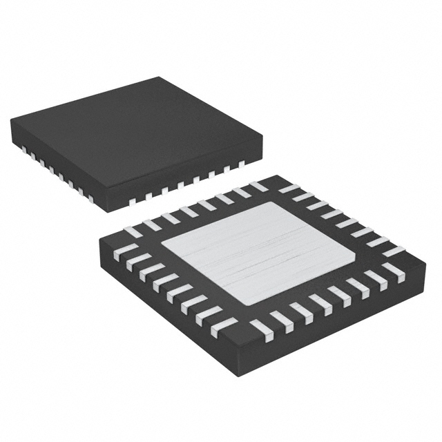
32-lead, Thin (1.0mm) Plastic Quad Flat Package (TQFP)
32MS1
32-pad, 5.0x5.0x0.9mm body, Lead Pitch 0.50mm, Very-thin Fine pitch, Quad Flat No Lead Package
(VQFN)
© 2017 Microchip Technology Inc.
Datasheet Summary
40001907A-page 6
�ATmega328PB
4.
Block Diagram
Figure 4-1. Block Diagram
SRAM
debugWire
PARPROG
CPU
OCD
SPIPROG
Clock generation
XTAL1 /
TOSC1
XTAL2 /
TOSC2
32.768kHz
XOSC
8MHz
Calib RC
External
clock
16MHz LP
XOSC
128kHz int
osc
Crystal failure detection
VCC
Power
Supervision
POR/BOD &
RESET
RESET
GND
NVM
programming
Power
management
and clock
control
Watchdog
Timer
PE[3:2], PC[5:0]
AREF
ADC[7:0]
AREF
ADC
PB[5:0], PE[1:0], PD[7:0]
PB[5:0], PE[1:0], PD[7:0], PE[3:2], PC[5:0]
X[15:0]
Y[23:0]
PTC
PE[3:0], PD[7:0], PC[6:0], PB[7:0]
PD3, PD2
PCINT[27:0]
INT[1:0]
PB1, PB2
PD5
PB0
OC1A/B
T1
ICP1
PB3
PD3
OC2A
OC2B
PD0, PD2
PE3
PE2
OC3A/B
T3
ICP3
PD1, PD2
PE1
PE0
OC4A/B
T4
ICP4
© 2017 Microchip Technology Inc.
FLASH
D
A
T
A
B
U
S
EEPROM
EEPROMIF
I/O
PORTS
I
N
/
O
U
T
GPIOR[2:0]
TC 0
D
A
T
A
B
U
S
(8-bit)
SPI 0
AC
Internal
Reference
EXTINT
USART 0
RxD0
TxD0
XCK0
PD0
PD1
PD4
TC 1
USART 1
RxD1
TxD1
XCK1
PB4
PB3
PB5
TC 2
TWI 0
SDA0
SCL0
PC4
PC5
TC 3
TWI 1
SDA1
SCL1
PE0
PE1
TC 4
SPI 1
MISO1
MOSI1
SCK1
SS1
PC0
PE3
PC1
PE2
(16-bit)
PB[7:0]
PC[6 :0]
PD[7:0]
PE[3:0]
T0
OC0A
OC0B
PD4
PD6
PD5
MISO0
MOSI0
SCK0
SS0
PB4
PB3
PB5
PB2
AIN0
AIN1
ACO
PD6
PD7
PE0
(8-bit async)
(16-bit)
(16-bit)
Datasheet Summary
40001907A-page 7
�ATmega328PB
Pin Configurations
PC6 (RESET)
PC5 (ADC5/PTCY/SCL0)
PC4 (ADC4/PTCY/SDA0)
PC3 (ADC3/PTCY)
PC2 (ADC2/PTCY)
29
28
27
26
25
Crystal/CLK
PD0 (PTCXY/OC3A/RXD0)
Analog
30
Digital
PD1 (PTCXY/OC4A/TXD0)
Programming/debug
31
Ground
PD2 (PTCXY/INT0/OC3B/OC4B)
Power
32
Figure 5-1. 32 TQFP Pinout ATmega328PB
GND
GND
5
20
AREF
(SCL1/T4/PTCXY) PE1
6
19
PE2 (ADC6/PTCY/ICP3/SS1)
(XTAL1/TOSC1) PB6
7
18
AVCC
(XTAL2/TOSC2) PB7
8
17
PB5 (PTCXY/XCK1/SCK0)
© 2017 Microchip Technology Inc.
16
21
(MISO0/RXD1/PTCXY) PB4
4
15
VCC
(MOSI0/TXD1/OC2A/PTCXY) PB3
PE3 (ADC7/PTCY/T3/MOSI1)
14
22
(SS0/OC1B/PTCXY) PB2
3
13
(SDA1/ICP4/ACO/PTCXY) PE0
(OC1A/PTCXY) PB1
PC0 (ADC0/PTCY/MISO1)
12
23
(ICP1/CLKO/PTCXY) PB0
2
11
(XCK0/T0/PTCXY) PD4
(PTCXY/AIN1) PD7
PC1 (ADC1/PTCY/SCK1)
10
24
(OC0A/PTCXY/AIN0) PD6
1
9
(OC2B/INT1/PTCXY) PD3
(OC0B/T1/PTCXY) PD5
5.
Datasheet Summary
40001907A-page 8
�ATmega328PB
PD2 (PTCXY/INT0/OC3B/OC4B)
PD1 (PTCXY/OC4A/TXD0)
PD0 (PTCXY/OC3A/RXD0)
PC6 (RESET)
PC5 (ADC5/PTCY/SCL0)
PC4 (ADC4/PTCY/SDA0)
PC3 (ADC3/PTCY)
PC2 (ADC2/PTCY)
32
31
30
29
28
27
26
25
Figure 5-2. 32 VQFN Pinout ATmega328PB
GND
5
20
AREF
(SCL1/T4/PTCXY) PE1
6
19
PE2 (ADC6/PTCY/ICP3/SS1)
(XTAL1/TOSC1) PB6
7
18
AVCC
(XTAL2/TOSC2) PB7
8
17
PB5 (PTCXY/XCK1/SCK0)
16
GND
(MISO0/RXD1/PTCXY) PB4
21
15
4
(MOSI0/TXD1/OC2A/PTCXY) PB3
VCC
14
PE3 (ADC7/PTCY/T3/MOSI1)
(SS0/OC1B/PTCXY) PB2
22
13
3
(OC1A/PTCXY) PB1
(SDA1/ICP4/ACO/PTCXY) PE0
12
PC0 (ADC0/PTCY/MISO1)
(ICP1/CLKO/PTCXY) PB0
23
11
2
(PTCXY/AIN1) PD7
(XCK0/T0/PTCXY) PD4
10
PC1 (ADC1/PTCY/SCK1)
(OC0A/PTCXY/AIN0) PD6
24
9
1
(OC0B/T1/PTCXY) PD5
(OC2B/INT1/PTCXY) PD3
Bottom pad should be
soldered to ground
5.1
Pin Descriptions
5.1.1
VCC
Digital supply voltage.
5.1.2
GND
Ground.
5.1.3
Port B (PB[7:0]) XTAL1/XTAL2/TOSC1/TOSC2
Port B is an 8-bit bi-directional I/O port with internal pull-up resistors (selected for each pin). The Port B
output buffers have symmetrical drive characteristics with both high sink and source capability. As inputs,
© 2017 Microchip Technology Inc.
Datasheet Summary
40001907A-page 9
�ATmega328PB
Port B pins that are externally pulled low will source current if the pull-up resistors are activated. The Port
B pins are tri-stated during a reset condition even if the clock is not running.
Depending on the clock selection fuse settings, PB6 can be used as input to the inverting Oscillator
amplifier and input to the internal clock operating circuit.
Depending on the clock selection fuse settings, PB7 can be used as output from the inverting Oscillator
amplifier.
If the Internal Calibrated RC Oscillator is used as chip clock source, PB[7:6] is used as TOSC[2:1] input
for the Asynchronous Timer/Counter2 if the AS2 bit in ASSR is set.
5.1.4
Port C (PC[5:0])
Port C is a 7-bit bi-directional I/O port with internal pull-up resistors (selected for each pin). The PC[5:0]
output buffers have symmetrical drive characteristics with both high sink and source capability. As inputs,
Port C pins that are externally pulled low will source current if the pull-up resistors are activated. The Port
C pins are tri-stated during a reset condition even if the clock is not running.
5.1.5
PC6/RESET
If the RSTDISBL Fuse is programmed, PC6 is used as an I/O pin. Note that the electrical characteristics
of PC6 differ from those of the other pins of Port C.
If the RSTDISBL Fuse is unprogrammed, PC6 is used as a Reset input. A low level on this pin for longer
than the minimum pulse length will generate a Reset, even if the clock is not running. Shorter pulses are
not guaranteed to generate a Reset.
The various special features of Port C are elaborated in the Alternate Functions of Port C section.
5.1.6
Port D (PD[7:0])
Port D is an 8-bit bi-directional I/O port with internal pull-up resistors (selected for each pin). The Port D
output buffers have symmetrical drive characteristics with both high sink and source capability. As inputs,
Port D pins that are externally pulled low will source current if the pull-up resistors are activated. The Port
D pins are tri-stated during a reset condition even if the clock is not running.
5.1.7
Port E (PE[3:0])
Port E is an 4-bit bi-directional I/O port with internal pull-up resistors (selected for each pin). The Port E
output buffers have symmetrical drive characteristics with both high sink and source capability. As inputs,
Port E pins that are externally pulled low will source current if the pull-up resistors are activated. The Port
E pins are tri-stated during a reset condition even if the clock is not running.
5.1.8
AVCC
AVCC is the supply voltage pin for the A/D Converter, PC[3:0], and PE[3:2]. It should be externally
connected to VCC, even if the ADC is not used. If the ADC is used, it should be connected to VCC through
a low-pass filter. Note that PC[6:4] use digital supply voltage, VCC.
5.1.9
AREF
AREF is the analog reference pin for the A/D Converter.
5.1.10
ADC[7:6] (TQFP and VFQFN Package Only)
In the TQFP and VFQFN package, ADC[7:6] serve as analog inputs to the A/D converter. These pins are
powered from the analog supply and serve as 10-bit ADC channels.
© 2017 Microchip Technology Inc.
Datasheet Summary
40001907A-page 10
�ATmega328PB
6.
I/O Multiplexing
Each pin is by default controlled by the PORT as a general purpose I/O and alternatively it can be
assigned to one of the peripheral functions.
The following table describes the peripheral signals multiplexed to the PORT I/O pins.
Table 6-1. PORT Function Multiplexing
No
PAD
EXTINT
PCINT
1
PD[3]
INT1
2
ADC/AC
PTC X
PTC Y
PCINT19
X3
Y11
OC2B
PD[4]
PCINT20
X4
Y12
T0
3
PE[0]
PCINT24
X8
Y16
ICP4
SDA1
4
VCC
5
GND
6
PE[1]
PCINT25
X9
Y17
TC4
SCL1
7
PB[6]
PCINT6
XTAL1/TOSC1
8
PB[7]
PCINT7
XTAL2/TOSC2
9
PD[5]
PCINT21
10
PD[6]
PCINT22
11
PD[7]
PCINT23
12
PB[0]
13
ACO
OSC
T/C
X5
Y13
OC0B / T1
AIN0
X6
Y14
OC0A
AIN1
X7
Y15
PCINT0
X10
Y18
PB[1]
PCINT1
X11
Y19
OC1A
14
PB[2]
PCINT2
X12
Y20
OC1B
15
PB[3]
PCINT3
X13
Y21
OC2A
16
PB[4]
PCINT4
X14
17
PB[5]
PCINT5
X15
18
AVCC
19
PE[2]
20
AREF
21
GND
22
CLKO
USART
I2C
SPI
XCK0
ICP1
SS0
TXD1
MOSI0
Y22
RXD1
MISO0
Y23
XCK1
SCK0
PCINT26
ADC6
Y6
ICP3
SS1
PE[3]
PCINT27
ADC7
Y7
T3
MOSI1
23
PC[0]
PCINT8
ADC0
Y0
MISO1
24
PC[1]
PCINT9
ADC1
Y1
SCK1
25
PC[2]
PCINT10
ADC2
Y2
26
PC[3]
PCINT11
ADC3
Y3
27
PC[4]
PCINT12
ADC4
Y4
SDA0
28
PC[5]
PCINT13
ADC5
Y5
SCL0
29
PC[6]/RESET
PCINT14
30
PD[0]
PCINT16
X0
Y8
OC3A
RXD0
31
PD[1]
PCINT17
X1
Y9
OC4A
TXD0
32
PD[2]
PCINT18
X2
Y10
OC3B / OC4B
INT0
© 2017 Microchip Technology Inc.
Datasheet Summary
40001907A-page 11
�ATmega328PB
7.
Resources
A comprehensive set of development tools, application notes, and datasheets are available for download
on http://www.microchip.com/design-centers/8-bit/microchip-avr-mcus.
© 2017 Microchip Technology Inc.
Datasheet Summary
40001907A-page 12
�ATmega328PB
8.
About Code Examples
This documentation contains simple code examples that briefly show how to use various parts of the
device. These code examples assume that the part specific header file is included before compilation. Be
aware that not all C compiler vendors include bit definitions in the header files and interrupt handling in C
is compiler dependent. Confirm with the C compiler documentation for more details.
For I/O Registers located in extended I/O map, “IN”, “OUT”, “SBIS”, “SBIC”, “CBI”, and “SBI” instructions
must be replaced with instructions that allow access to extended I/O. Typically “LDS” and “STS”
combined with “SBRS”, “SBRC”, “SBR”, and “CBR”.
© 2017 Microchip Technology Inc.
Datasheet Summary
40001907A-page 13
�ATmega328PB
The Microchip Web Site
Microchip provides online support via our web site at http://www.microchip.com/. This web site is used as
a means to make files and information easily available to customers. Accessible by using your favorite
Internet browser, the web site contains the following information:
•
•
•
Product Support – Data sheets and errata, application notes and sample programs, design
resources, user’s guides and hardware support documents, latest software releases and archived
software
General Technical Support – Frequently Asked Questions (FAQ), technical support requests,
online discussion groups, Microchip consultant program member listing
Business of Microchip – Product selector and ordering guides, latest Microchip press releases,
listing of seminars and events, listings of Microchip sales offices, distributors and factory
representatives
Customer Change Notification Service
Microchip’s customer notification service helps keep customers current on Microchip products.
Subscribers will receive e-mail notification whenever there are changes, updates, revisions or errata
related to a specified product family or development tool of interest.
To register, access the Microchip web site at http://www.microchip.com/. Under “Support”, click on
“Customer Change Notification” and follow the registration instructions.
Customer Support
Users of Microchip products can receive assistance through several channels:
•
•
•
•
Distributor or Representative
Local Sales Office
Field Application Engineer (FAE)
Technical Support
Customers should contact their distributor, representative or Field Application Engineer (FAE) for support.
Local sales offices are also available to help customers. A listing of sales offices and locations is included
in the back of this document.
Technical support is available through the web site at: http://www.microchip.com/support
Microchip Devices Code Protection Feature
Note the following details of the code protection feature on Microchip devices:
•
•
•
•
Microchip products meet the specification contained in their particular Microchip Data Sheet.
Microchip believes that its family of products is one of the most secure families of its kind on the
market today, when used in the intended manner and under normal conditions.
There are dishonest and possibly illegal methods used to breach the code protection feature. All of
these methods, to our knowledge, require using the Microchip products in a manner outside the
operating specifications contained in Microchip’s Data Sheets. Most likely, the person doing so is
engaged in theft of intellectual property.
Microchip is willing to work with the customer who is concerned about the integrity of their code.
© 2017 Microchip Technology Inc.
Datasheet Summary
40001907A-page 14
�ATmega328PB
•
Neither Microchip nor any other semiconductor manufacturer can guarantee the security of their
code. Code protection does not mean that we are guaranteeing the product as “unbreakable.”
Code protection is constantly evolving. We at Microchip are committed to continuously improving the
code protection features of our products. Attempts to break Microchip’s code protection feature may be a
violation of the Digital Millennium Copyright Act. If such acts allow unauthorized access to your software
or other copyrighted work, you may have a right to sue for relief under that Act.
Legal Notice
Information contained in this publication regarding device applications and the like is provided only for
your convenience and may be superseded by updates. It is your responsibility to ensure that your
application meets with your specifications. MICROCHIP MAKES NO REPRESENTATIONS OR
WARRANTIES OF ANY KIND WHETHER EXPRESS OR IMPLIED, WRITTEN OR ORAL, STATUTORY
OR OTHERWISE, RELATED TO THE INFORMATION, INCLUDING BUT NOT LIMITED TO ITS
CONDITION, QUALITY, PERFORMANCE, MERCHANTABILITY OR FITNESS FOR PURPOSE.
Microchip disclaims all liability arising from this information and its use. Use of Microchip devices in life
support and/or safety applications is entirely at the buyer’s risk, and the buyer agrees to defend,
indemnify and hold harmless Microchip from any and all damages, claims, suits, or expenses resulting
from such use. No licenses are conveyed, implicitly or otherwise, under any Microchip intellectual
property rights unless otherwise stated.
Trademarks
The Microchip name and logo, the Microchip logo, AnyRate, AVR, AVR logo, AVR Freaks, BeaconThings,
BitCloud, CryptoMemory, CryptoRF, dsPIC, FlashFlex, flexPWR, Heldo, JukeBlox, KeeLoq, KeeLoq logo,
Kleer, LANCheck, LINK MD, maXStylus, maXTouch, MediaLB, megaAVR, MOST, MOST logo, MPLAB,
OptoLyzer, PIC, picoPower, PICSTART, PIC32 logo, Prochip Designer, QTouch, RightTouch, SAM-BA,
SpyNIC, SST, SST Logo, SuperFlash, tinyAVR, UNI/O, and XMEGA are registered trademarks of
Microchip Technology Incorporated in the U.S.A. and other countries.
ClockWorks, The Embedded Control Solutions Company, EtherSynch, Hyper Speed Control, HyperLight
Load, IntelliMOS, mTouch, Precision Edge, and Quiet-Wire are registered trademarks of Microchip
Technology Incorporated in the U.S.A.
Adjacent Key Suppression, AKS, Analog-for-the-Digital Age, Any Capacitor, AnyIn, AnyOut, BodyCom,
chipKIT, chipKIT logo, CodeGuard, CryptoAuthentication, CryptoCompanion, CryptoController,
dsPICDEM, dsPICDEM.net, Dynamic Average Matching, DAM, ECAN, EtherGREEN, In-Circuit Serial
Programming, ICSP, Inter-Chip Connectivity, JitterBlocker, KleerNet, KleerNet logo, Mindi, MiWi,
motorBench, MPASM, MPF, MPLAB Certified logo, MPLIB, MPLINK, MultiTRAK, NetDetach, Omniscient
Code Generation, PICDEM, PICDEM.net, PICkit, PICtail, PureSilicon, QMatrix, RightTouch logo, REAL
ICE, Ripple Blocker, SAM-ICE, Serial Quad I/O, SMART-I.S., SQI, SuperSwitcher, SuperSwitcher II, Total
Endurance, TSHARC, USBCheck, VariSense, ViewSpan, WiperLock, Wireless DNA, and ZENA are
trademarks of Microchip Technology Incorporated in the U.S.A. and other countries.
SQTP is a service mark of Microchip Technology Incorporated in the U.S.A.
Silicon Storage Technology is a registered trademark of Microchip Technology Inc. in other countries.
GestIC is a registered trademark of Microchip Technology Germany II GmbH & Co. KG, a subsidiary of
Microchip Technology Inc., in other countries.
All other trademarks mentioned herein are property of their respective companies.
©
2017, Microchip Technology Incorporated, Printed in the U.S.A., All Rights Reserved.
© 2017 Microchip Technology Inc.
Datasheet Summary
40001907A-page 15
�ATmega328PB
ISBN: 978-1-5224-1683-8
Quality Management System Certified by DNV
ISO/TS 16949
Microchip received ISO/TS-16949:2009 certification for its worldwide headquarters, design and wafer
fabrication facilities in Chandler and Tempe, Arizona; Gresham, Oregon and design centers in California
®
®
and India. The Company’s quality system processes and procedures are for its PIC MCUs and dsPIC
®
DSCs, KEELOQ code hopping devices, Serial EEPROMs, microperipherals, nonvolatile memory and
analog products. In addition, Microchip’s quality system for the design and manufacture of development
systems is ISO 9001:2000 certified.
© 2017 Microchip Technology Inc.
Datasheet Summary
40001907A-page 16
�Worldwide Sales and Service
AMERICAS
ASIA/PACIFIC
ASIA/PACIFIC
EUROPE
Corporate Office
Asia Pacific Office
China - Xiamen
Austria - Wels
2355 West Chandler Blvd.
Suites 3707-14, 37th Floor
Tel: 86-592-2388138
Tel: 43-7242-2244-39
Chandler, AZ 85224-6199
Tower 6, The Gateway
Fax: 86-592-2388130
Fax: 43-7242-2244-393
Tel: 480-792-7200
Harbour City, Kowloon
China - Zhuhai
Denmark - Copenhagen
Fax: 480-792-7277
Hong Kong
Tel: 86-756-3210040
Tel: 45-4450-2828
Technical Support:
Tel: 852-2943-5100
Fax: 86-756-3210049
Fax: 45-4485-2829
http://www.microchip.com/
Fax: 852-2401-3431
India - Bangalore
Finland - Espoo
support
Australia - Sydney
Tel: 91-80-3090-4444
Tel: 358-9-4520-820
Web Address:
Tel: 61-2-9868-6733
Fax: 91-80-3090-4123
France - Paris
www.microchip.com
Fax: 61-2-9868-6755
India - New Delhi
Tel: 33-1-69-53-63-20
Atlanta
China - Beijing
Tel: 91-11-4160-8631
Fax: 33-1-69-30-90-79
Duluth, GA
Tel: 86-10-8569-7000
Fax: 91-11-4160-8632
France - Saint Cloud
Tel: 678-957-9614
Fax: 86-10-8528-2104
India - Pune
Tel: 33-1-30-60-70-00
Fax: 678-957-1455
China - Chengdu
Tel: 91-20-3019-1500
Germany - Garching
Austin, TX
Tel: 86-28-8665-5511
Japan - Osaka
Tel: 49-8931-9700
Tel: 512-257-3370
Fax: 86-28-8665-7889
Tel: 81-6-6152-7160
Germany - Haan
Boston
China - Chongqing
Fax: 81-6-6152-9310
Tel: 49-2129-3766400
Westborough, MA
Tel: 86-23-8980-9588
Japan - Tokyo
Germany - Heilbronn
Tel: 774-760-0087
Fax: 86-23-8980-9500
Tel: 81-3-6880- 3770
Tel: 49-7131-67-3636
Fax: 774-760-0088
China - Dongguan
Fax: 81-3-6880-3771
Germany - Karlsruhe
Chicago
Tel: 86-769-8702-9880
Korea - Daegu
Tel: 49-721-625370
Itasca, IL
China - Guangzhou
Tel: 82-53-744-4301
Germany - Munich
Tel: 630-285-0071
Tel: 86-20-8755-8029
Fax: 82-53-744-4302
Tel: 49-89-627-144-0
Fax: 630-285-0075
China - Hangzhou
Korea - Seoul
Fax: 49-89-627-144-44
Dallas
Tel: 86-571-8792-8115
Tel: 82-2-554-7200
Germany - Rosenheim
Addison, TX
Fax: 86-571-8792-8116
Fax: 82-2-558-5932 or
Tel: 49-8031-354-560
Tel: 972-818-7423
China - Hong Kong SAR
82-2-558-5934
Israel - Ra’anana
Fax: 972-818-2924
Tel: 852-2943-5100
Malaysia - Kuala Lumpur
Tel: 972-9-744-7705
Detroit
Fax: 852-2401-3431
Tel: 60-3-6201-9857
Italy - Milan
Novi, MI
China - Nanjing
Fax: 60-3-6201-9859
Tel: 39-0331-742611
Tel: 248-848-4000
Tel: 86-25-8473-2460
Malaysia - Penang
Fax: 39-0331-466781
Houston, TX
Fax: 86-25-8473-2470
Tel: 60-4-227-8870
Italy - Padova
Tel: 281-894-5983
China - Qingdao
Fax: 60-4-227-4068
Tel: 39-049-7625286
Indianapolis
Tel: 86-532-8502-7355
Philippines - Manila
Netherlands - Drunen
Noblesville, IN
Fax: 86-532-8502-7205
Tel: 63-2-634-9065
Tel: 31-416-690399
Tel: 317-773-8323
China - Shanghai
Fax: 63-2-634-9069
Fax: 31-416-690340
Fax: 317-773-5453
Tel: 86-21-3326-8000
Singapore
Norway - Trondheim
Tel: 317-536-2380
Fax: 86-21-3326-8021
Tel: 65-6334-8870
Tel: 47-7289-7561
Los Angeles
China - Shenyang
Fax: 65-6334-8850
Poland - Warsaw
Mission Viejo, CA
Tel: 86-24-2334-2829
Taiwan - Hsin Chu
Tel: 48-22-3325737
Tel: 949-462-9523
Fax: 86-24-2334-2393
Tel: 886-3-5778-366
Romania - Bucharest
Fax: 949-462-9608
China - Shenzhen
Fax: 886-3-5770-955
Tel: 40-21-407-87-50
Tel: 951-273-7800
Tel: 86-755-8864-2200
Taiwan - Kaohsiung
Spain - Madrid
Raleigh, NC
Fax: 86-755-8203-1760
Tel: 886-7-213-7830
Tel: 34-91-708-08-90
Tel: 919-844-7510
China - Wuhan
Taiwan - Taipei
Fax: 34-91-708-08-91
New York, NY
Tel: 86-27-5980-5300
Tel: 886-2-2508-8600
Sweden - Gothenberg
Tel: 631-435-6000
Fax: 86-27-5980-5118
Fax: 886-2-2508-0102
Tel: 46-31-704-60-40
San Jose, CA
China - Xian
Thailand - Bangkok
Sweden - Stockholm
Tel: 408-735-9110
Tel: 86-29-8833-7252
Tel: 66-2-694-1351
Tel: 46-8-5090-4654
Tel: 408-436-4270
Fax: 86-29-8833-7256
Fax: 66-2-694-1350
UK - Wokingham
Canada - Toronto
Tel: 44-118-921-5800
Tel: 905-695-1980
Fax: 44-118-921-5820
Fax: 905-695-2078
© 2017 Microchip Technology Inc.
Datasheet Summary
40001907A-page 17
�