Features
• High Performance, Low Power AVR® 8-bit Microcontroller
• Advanced RISC Architecture
•
•
•
•
•
•
•
•
•
– 124 Powerful Instructions - Most Single Clock Cycle Execution
– 32 x 8 General Purpose Working Registers
– Fully Static Operation
– Up to 1 MIPS Throughput at 1 MHz
Nonvolatile Program and Data Memories
– 40K Bytes of In-System Self-Programmable Flash, Endurance: 10,000 Write/Erase
Cycles
– Optional Boot Code Section with Independent Lock Bits
In-System Programming by On-chip Boot Program
True Read-While-Write Operation
– 512 bytes EEPROM, Endurance: 100,000 Write/Erase Cycles
– 2K Bytes Internal SRAM
– Programming Lock for Software Security
On-chip Debugging
– Extensive On-chip Debug Support
– Available through JTAG interface
Battery Management Features
– Two, Three, or Four Cells in Series
– Deep Under-voltage Protection
– Over-current Protection (Charge and Discharge)
– Short-circuit Protection (Discharge)
– Integrated Cell Balancing FETs
– High Voltage Outputs to Drive Charge/Precharge/Discharge FETs
Peripheral Features
– One 8-bit Timer/Counter with Separate Prescaler, Compare Mode, and PWM
– One 16-bit Timer/Counter with Separate Prescaler and Compare Mode
– 12-bit Voltage ADC, Eight External and Two Internal ADC Inputs
– High Resolution Coulomb Counter ADC for Current Measurements
– TWI Serial Interface for SM-Bus
– Programmable Wake-up Timer
– Programmable Watchdog Timer
Special Microcontroller Features
– Power-on Reset
– On-chip Voltage Regulator
– External and Internal Interrupt Sources
– Four Sleep Modes: Idle, Power-save, Power-down, and Power-off
Packages
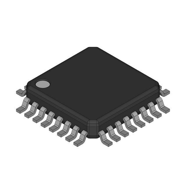
– 48-pin LQFP
Operating Voltage: 4.0 - 25V
Maximum Withstand Voltage (High-voltage pins): 28V
Temperature Range: -30°C to 85°C
– Speed Grade: 1 MHz
8-bit
Microcontroller
with 40K Bytes
In-System
Programmable
Flash
ATmega406
Preliminary
Summary
2548FS–AVR–03/2013
�1. Pin Configurations
Figure 1-1.
Pinout ATmega406.
48
47
46
45
44
43
42
41
40
39
38
37
NNI
NI
PI
PPI
VREFGND
VREF
NV
PV1
PV2
PV3
PV4
GND
Top View
36
35
34
33
32
31
30
29
28
27
26
25
1
2
3
4
5
6
7
8
9
10
11
12
PVT
OD
VFET
OC
OPC
BATT
PC0
GND
PD1
PD0 (T0)
PB7 (OC0B/PCINT15)
PB6 (OC0A/PCINT14)
RESET
XTAL1
XTAL2
GND
(TDO/PCINT8) PB0
(TDI/PCINT9) PB1
(TMS/PCINT10) PB2
(TCK/PCINT11) PB3
(PCINT12) PB4
(PCINT13) PB5
SCL
SDA
13
14
15
16
17
18
19
20
21
22
23
24
SGND
(ADC0/PCINT0) PA0
(ADC1/PCINT1) PA1
(ADC2/PCINT2) PA2
(ADC3/PCINT3) PA3
VREG
VCC
GND
(ADC4/INT0/PCINT4) PA4
(INT1/PCINT5) PA5
(INT2/PCINT6) PA6
(INT3/PCINT7) PA7
1.1
Disclaimer
Typical values contained in this datasheet are based on simulations and characterization of
other AVR microcontrollers manufactured on the same process technology. Min and Max values
will be available after the device is characterized.
2
ATmega406
2548FS–AVR–03/2013
�ATmega406
2. Overview
The ATmega406 is a low-power CMOS 8-bit microcontroller based on the AVR enhanced RISC
architecture. By executing powerful instructions in a single clock cycle, the ATmega406
achieves throughputs approaching 1 MIPS at 1 MHz.
2.1
Block Diagram
Figure 2-1.
Block Diagram
PD1..0
PB7..0
PORTD (2)
PORTB (8)
XTAL1
Oscillator
Circuits /
Clock
Generation
XTAL2
Watchdog
Oscillator
VCC
RESET
OPC
OC
OD
FET
Control
Battery
Protection
PPI
NNI
PVT
PV4
PV3
PV2
PV1
NV
Wake-Up
Timer
JTAG
8 bit T/C0
Cell
Balancing
Flash
SRAM
16 bit T/C1
Voltage
ADC
EEPROM
Voltage
Reference
Watchdog
Timer
Power
Supervision
POR &
RESET
CPU
SGND
VREF
VREFGND
GND
BATT
VFET
VREG
Coulumb
Counter ADC
Charger
Detect
PI
NI
DATA BUS
Voltage
Regulator
TWI
PORTC (1)
PORTA (8)
PA3..0
SCL
SCA
PC0
PA7..0
The ATmega406 provides the following features: a Voltage Regulator, dedicated Battery Protection Circuitry, integrated cell balancing FETs, high-voltage analog front-end, and an MCU with
two ADCs with On-chip voltage reference for battery fuel gauging.
The voltage regulator operates at a wide range of voltages, 4.0 - 25 volts. This voltage is regulated to a constant supply voltage of nominally 3.3 volts for the integrated logic and analog
functions.
The battery protection monitors the battery voltage and charge/discharge current to detect illegal
conditions and protect the battery from these when required. The illegal conditions are deep
under-voltage during discharging, short-circuit during discharging and over-current during charging and discharging.
3
2548FS–AVR–03/2013
�The integrated cell balancing FETs allow cell balancing algorithms to be implemented in
software.
The MCU provides the following features: 40K bytes of In-System Programmable Flash with
Read-While-Write capabilities, 512 bytes EEPROM, 2K byte SRAM, 32 general purpose working
registers, 18 general purpose I/O lines, 11 high-voltage I/O lines, a JTAG Interface for On-chip
Debugging support and programming, two flexible Timer/Counters with PWM and compare
modes, one Wake-up Timer, an SM-Bus compliant TWI module, internal and external interrupts,
a 12-bit Sigma Delta ADC for voltage and temperature measurements, a high resolution Sigma
Delta ADC for Coulomb Counting and instantaneous current measurements, a programmable
Watchdog Timer with internal Oscillator, and four software selectable power saving modes.
The AVR core combines a rich instruction set with 32 general purpose working registers. All the
32 registers are directly connected to the Arithmetic Logic Unit (ALU), allowing two independent
registers to be accessed in one single instruction executed in one clock cycle. The resulting
architecture is more code efficient while achieving throughputs up to ten times faster than conventional CISC microcontrollers.
The Idle mode stops the CPU while allowing the other chip function to continue functioning. The
Power-down mode allows the voltage regulator, battery protection, regulator current detection,
Watchdog Timer, and Wake-up Timer to operate, while disabling all other chip functions until the
next Interrupt or Hardware Reset. In Power-save mode, the Wake-up Timer and Coulomb Counter ADC continues to run.
The device is manufactured using Atmel’s high voltage high density non-volatile memory technology. The On-chip ISP Flash allows the program memory to be reprogrammed In-System, by
a conventional non-volatile memory programmer or by an On-chip Boot program running on the
AVR core. The Boot program can use any interface to download the application program in the
Application Flash memory. Software in the Boot Flash section will continue to run while the
Application Flash section is updated, providing true Read-While-Write operation. By combining
an 8-bit RISC CPU with In-System Self-Programmable Flash, fuel gauging ADCs, dedicated battery protection circuitry, Cell Balancing FETs, and a voltage regulator on a monolithic chip, the
Atmel ATmega406 is a powerful microcontroller that provides a highly flexible and cost effective
solution for Li-ion Smart Battery applications.
The ATmega406 AVR is supported with a full suite of program and system development tools
including: C Compilers, Macro Assemblers, Program Debugger/Simulators, and On-chip
Debugger.
4
ATmega406
2548FS–AVR–03/2013
�ATmega406
2.2
2.2.1
Pin Descriptions
VFET
High voltage supply pin. This pin is used as supply for the internal voltage regulator, described in
”Voltage Regulator” on page 114. In addition the voltage level on this pin is monitored by the battery protection circuit, for deep-under-voltage protection. For details, see ”Battery Protection” on
page 125.
2.2.2
VCC
Digital supply voltage. Normally connected to VREG.
2.2.3
VREG
Output from the internal Voltage Regulator. Used for external decoupling to ensure stable regulator operation. For details, see ”Voltage Regulator” on page 114.
2.2.4
VREF
Internal Voltage Reference for external decoupling. For details, see ”Voltage Reference and
Temperature Sensor” on page 121.
2.2.5
VREFGND
Ground for decoupling of Internal Voltage Reference. For details, see ”Voltage Reference and
Temperature Sensor” on page 121.
2.2.6
GND
Ground
2.2.7
SGND
Signal ground pin, used as reference for Voltage-ADC conversions. For details, see ”Voltage
ADC – 10-channel General Purpose 12-bit Sigma-Delta ADC” on page 116.
2.2.8
Port A (PA7:PA0)
PA3:PA0 serves as the analog inputs to the Voltage A/D Converter.
Port A also serves as a low-voltage 8-bit bi-directional I/O port with internal pull-up resistors
(selected for each bit). As inputs, Port A pins that are externally pulled low will source current if
the pull-up resistors are activated. The Port A pins are tri-stated when a reset condition becomes
active, even if the clock is not running.
Port A also serves the functions of various special features of the ATmega406 as listed in ”Alternate Functions of Port A” on page 68.
2.2.9
Port B (PB7:PB0)
Port B is a low-voltage 8-bit bi-directional I/O port with internal pull-up resistors (selected for
each bit). As inputs, Port B pins that are externally pulled low will source current if the pull-up
resistors are activated. The Port B pins are tri-stated when a reset condition becomes active,
even if the clock is not running.
Port B also serves the functions of various special features of the ATmega406 as listed in ”Alternate Functions of Port B” on page 70.
5
2548FS–AVR–03/2013
�2.2.10
Port C (PC0)
Port C is a high voltage Open Drain output port.
2.2.11
Port D (PD1:PD0)
Port D is a low-voltage 2-bit bi-directional I/O port with internal pull-up resistors (selected for
each bit). As inputs, Port D pins that are externally pulled low will source current if the pull-up
resistors are activated. The Port D pins are tri-stated when a reset condition becomes active,
even if the clock is not running.
Port D also serves the functions of various special features of the ATmega406 as listed in ”Alternate Functions of Port D” on page 72.
2.2.12
SCL
SMBUS clock, Open Drain bidirectional pin.
2.2.13
SDA
SMBUS data, Open Drain bidirectional pin.
2.2.14
OC/OD/OPC
High voltage output to drive external Charge/Discharge/Pre-charge FETs. For details, see ”FET
Control” on page 133.
2.2.15
PPI/NNI
Unfiltered positive/negative input from external current sense resistor, used by the battery protection circuit, for over-current and short-circuit detection. For details, see ”Battery Protection” on
page 125.
2.2.16
PI/NI
Filtered positive/negative input from external current sense resistor, used to by the Coulomb
Counter ADC to measure charge/discharge currents flowing in the battery pack. For details, see
”Coulomb Counter - Dedicated Fuel Gauging Sigma-delta ADC” on page 106.
2.2.17
NV/PV1/PV2/PV3/PV4
NV, PV1, PV2, PV3, and PV4 are the inputs for battery cells 1, 2, 3 and 4, used by the Voltage
ADC to measure each cell voltage. For details, see ”Voltage ADC – 10-channel General Purpose 12-bit Sigma-Delta ADC” on page 116.
2.2.18
PVT
PVT defines the pull-up level for the OD output.
2.2.19
BATT
Input for detecting when a charger is connected. This pin also defines the pull-up level for OC
and OPC outputs.
2.2.20
RESET
Reset input. A low level on this pin for longer than the minimum pulse length will generate a
reset, even if the clock is not running. The minimum pulse length is given in Table 11 on page
38. Shorter pulses are not guaranteed to generate a reset.
6
ATmega406
2548FS–AVR–03/2013
�ATmega406
2.2.21
XTAL1
Input to the inverting Oscillator amplifier.
2.2.22
XTAL2
Output from the inverting Oscillator amplifier.
3. Resources
A comprehensive set of development tools, application notes and datasheets are available for
download on http://www.atmel.com/avr.
7
2548FS–AVR–03/2013
�8
ATmega406
2548FS–AVR–03/2013
�ATmega406
4. Register Summary
Address
Name
Bit 7
Bit 6
Bit 5
Bit 4
Bit 3
Bit 2
Bit 1
Bit 0
(0xFF)
Reserved
–
–
–
–
–
–
–
–
Page
(0xFE)
Reserved
–
–
–
–
–
–
–
–
(0xFD)
Reserved
–
–
–
–
–
–
–
–
(0xFC)
Reserved
–
–
–
–
–
–
–
–
(0xFB)
Reserved
–
–
–
–
–
–
–
–
(0xFA)
Reserved
–
–
–
–
–
–
–
–
(0xF9)
Reserved
–
–
–
–
–
–
–
–
(0xF8)
BPPLR
–
–
–
–
–
–
BPPLE
BPPL
128
(0xF7)
BPCR
–
–
–
–
DUVD
SCD
DCD
CCD
128
(0xF6)
CBPTR
SCPT[3:0]
OCPT[3:0]
129
(0xF5)
BPOCD
DCDL[3:0]
CCDL[3:0]
130
(0xF4)
BPSCD
–
–
–
–
SCDL[3:0]
130
(0xF3)
BPDUV
–
–
DUVT1
DUVT0
DUDL[3:0]
131
(0xF2)
BPIR
DUVIF
COCIF
DOCIF
SCIF
DUVIE
COCIE
DOCIE
SCIE
132
(0xF1)
CBCR
–
–
–
–
CBE4
CBE3
CBE2
CBE1
137
(0xF0)
FCSR
–
–
PWMOC
PWMOPC
CPS
DFE
CFE
PFD
134
(0xEF)
Reserved
–
–
–
–
–
–
–
–
(0xEE)
Reserved
–
–
–
–
–
–
–
–
(0xED)
Reserved
–
–
–
–
–
–
–
–
(0xEC)
Reserved
–
–
–
–
–
–
–
–
(0xEB)
Reserved
–
–
–
–
–
–
–
–
(0xEA)
Reserved
–
–
–
–
–
–
–
–
(0xE9)
CADICH
CADIC[15:8]
111
(0xE8)
CADICL
CADIC[7:0]
111
(0xE7)
CADRDC
CADRDC[7:0]
112
(0xE6)
CADRCC
CADRCC[7:0]
(0xE5)
CADCSRB
–
CADACIE
CADRCIE
CADICIE
–
CADACIF
CADRCIF
CADICIF
110
(0xE4)
CADCSRA
CADEN
–
CADUB
CADAS1
CADAS0
CADSI1
CADSI0
CADSE
109
(0xE3)
CADAC3
CADAC[31:24]
111
(0xE2)
CADAC2
CADAC[23:16]
111
(0xE1)
CADAC1
CADAC[15:8]
111
(0xE0)
CADAC0
CADAC[7:0]
(0xDF)
Reserved
–
–
–
–
–
–
–
–
112
111
(0xDE)
Reserved
–
–
–
–
–
–
–
–
(0xDD)
Reserved
–
–
–
–
–
–
–
–
(0xDC)
Reserved
–
–
–
–
–
–
–
–
(0xDB)
Reserved
–
–
–
–
–
–
–
–
(0xDA)
Reserved
–
–
–
–
–
–
–
–
(0xD9)
Reserved
–
–
–
–
–
–
–
–
(0xD8)
Reserved
–
–
–
–
–
–
–
–
(0xD7)
Reserved
–
–
–
–
–
–
–
–
(0xD6)
Reserved
–
–
–
–
–
–
–
–
(0xD5)
Reserved
–
–
–
–
–
–
–
–
(0xD4)
Reserved
–
–
–
–
–
–
–
–
(0xD3)
Reserved
–
–
–
–
–
–
–
–
(0xD2)
Reserved
–
–
–
–
–
–
–
–
(0xD1)
BGCRR
BGCR7
BGCR6
BGCR5
BGCR4
BGCR3
BGCR2
BGCR1
BGCR0
123
(0xD0)
BGCCR
BGEN
–
BGCC5
BGCC4
BGCC3
BGCC2
BGCC1
BGCC0
123
(0xCF)
Reserved
–
–
–
–
–
–
–
–
(0xCE)
Reserved
–
–
–
–
–
–
–
–
(0xCD)
Reserved
–
–
–
–
–
–
–
–
(0xCC)
Reserved
–
–
–
–
–
–
–
–
(0xCB)
Reserved
–
–
–
–
–
–
–
–
(0xCA)
Reserved
–
–
–
–
–
–
–
–
(0xC9)
Reserved
–
–
–
–
–
–
–
–
(0xC8)
Reserved
–
–
–
–
–
–
–
–
(0xC7)
Reserved
–
–
–
–
–
–
–
–
(0xC6)
Reserved
–
–
–
–
–
–
–
–
(0xC5)
Reserved
–
–
–
–
–
–
–
–
(0xC4)
Reserved
–
–
–
–
–
–
–
–
(0xC3)
Reserved
–
–
–
–
–
–
–
–
(0xC2)
Reserved
–
–
–
–
–
–
–
–
(0xC1)
Reserved
–
–
–
–
–
–
–
–
(0xC0)
CCSR
–
–
–
–
–
–
XOE
ACS
29
9
2548FS–AVR–03/2013
�Address
Name
Bit 7
Bit 6
Bit 5
Bit 4
Bit 3
Bit 2
Bit 1
Bit 0
(0xBF)
Reserved
–
–
–
–
–
–
–
–
TWBCIF
TWBCIE
–
–
–
TWBDT1
TWBDT0
TWBCIP
169
–
150
10
(0xBE)
TWBCSR
(0xBD)
TWAMR
(0xBC)
TWCR
(0xBB)
TWDR
TWAM[6:0]
TWINT
TWEA
TWSTA
TWSTO
TWWC
TWEN
–
TWIE
2–wire Serial Interface Data Register
Page
147
149
(0xBA)
TWAR
(0xB9)
TWSR
TWA[6:0]
TWGCE
(0xB8)
TWBR
(0xB7)
Reserved
–
–
–
–
–
–
–
(0xB6)
Reserved
–
–
–
–
–
–
–
–
(0xB5)
Reserved
–
–
–
–
–
–
–
–
(0xB4)
Reserved
–
–
–
–
–
–
–
–
(0xB3)
Reserved
–
–
–
–
–
–
–
–
(0xB2)
Reserved
–
–
–
–
–
–
–
–
(0xB1)
Reserved
–
–
–
–
–
–
–
–
(0xB0)
Reserved
–
–
–
–
–
–
–
–
(0xAF)
Reserved
–
–
–
–
–
–
–
–
(0xAE)
Reserved
–
–
–
–
–
–
–
–
(0xAD)
Reserved
–
–
–
–
–
–
–
–
(0xAC)
Reserved
–
–
–
–
–
–
–
–
(0xAB)
Reserved
–
–
–
–
–
–
–
–
(0xAA)
Reserved
–
–
–
–
–
–
–
–
(0xA9)
Reserved
–
–
–
–
–
–
–
–
(0xA8)
Reserved
–
–
–
–
–
–
–
–
(0xA7)
Reserved
–
–
–
–
–
–
–
–
(0xA6)
Reserved
–
–
–
–
–
–
–
–
(0xA5)
Reserved
–
–
–
–
–
–
–
–
(0xA4)
Reserved
–
–
–
–
–
–
–
–
(0xA3)
Reserved
–
–
–
–
–
–
–
–
(0xA2)
Reserved
–
–
–
–
–
–
–
–
(0xA1)
Reserved
–
–
–
–
–
–
–
–
(0xA0)
Reserved
–
–
–
–
–
–
–
–
(0x9F)
Reserved
–
–
–
–
–
–
–
–
(0x9E)
Reserved
–
–
–
–
–
–
–
–
(0x9D)
Reserved
–
–
–
–
–
–
–
–
(0x9C)
Reserved
–
–
–
–
–
–
–
–
(0x9B)
Reserved
–
–
–
–
–
–
–
–
(0x9A)
Reserved
–
–
–
–
–
–
–
–
(0x99)
Reserved
–
–
–
–
–
–
–
–
(0x98)
Reserved
–
–
–
–
–
–
–
–
(0x97)
Reserved
–
–
–
–
–
–
–
–
(0x96)
Reserved
–
–
–
–
–
–
–
–
(0x95)
Reserved
–
–
–
–
–
–
–
–
(0x94)
Reserved
–
–
–
–
–
–
–
–
(0x93)
Reserved
–
–
–
–
–
–
–
–
(0x92)
Reserved
–
–
–
–
–
–
–
–
(0x91)
Reserved
–
–
–
–
–
–
–
–
(0x90)
Reserved
–
–
–
–
–
–
–
–
(0x8F)
Reserved
–
–
–
–
–
–
–
–
(0x8E)
Reserved
–
–
–
–
–
–
–
–
(0x8D)
Reserved
–
–
–
–
–
–
–
–
(0x8C)
Reserved
–
–
–
–
–
–
–
–
(0x8B)
Reserved
–
–
–
–
–
–
–
–
(0x8A)
Reserved
–
–
–
–
–
–
–
–
(0x89)
OCR1AH
Timer/Counter1 – Output Compare Register A High Byte
101
(0x88)
OCR1AL
Timer/Counter1 – Output Compare Register A Low Byte
101
(0x87)
Reserved
–
–
–
–
–
–
–
–
(0x86)
Reserved
–
–
–
–
–
–
–
–
(0x85)
TCNT1H
Timer/Counter1 – Counter Register High Byte
101
(0x84)
TCNT1L
Timer/Counter1 – Counter Register Low Byte
101
(0x83)
Reserved
–
–
–
–
–
–
–
(0x82)
Reserved
–
–
–
–
–
–
–
–
(0x81)
TCCR1B
–
–
–
–
CTC1
CS12
CS11
CS10
(0x80)
Reserved
–
–
–
–
–
–
–
–
(0x7F)
Reserved
–
–
–
–
–
–
–
–
(0x7E)
DIDR0
–
–
–
–
VADC3D
VADC2D
VADC1D
VADC0D
TWS[7:3]
–
TWPS1
TWPS0
2–wire Serial Interface Bit Rate Register
149
148
147
–
100
120
ATmega406
2548FS–AVR–03/2013
�ATmega406
Address
Name
Bit 7
Bit 6
Bit 5
Bit 4
Bit 3
Bit 2
Bit 1
Bit 0
(0x7D)
Reserved
–
–
–
–
–
–
–
–
(0x7C)
VADMUX
–
–
–
–
VADMUX3
VADMUX2
VADMUX1
VADMUX0
(0x7B)
Reserved
–
–
–
–
–
–
–
–
(0x7A)
VADCSR
–
–
–
–
VADEN
VADSC
VADCCIF
VADCCIE
(0x79)
VADCH
–
–
–
–
(0x78)
VADCL
(0x77)
Reserved
–
–
–
–
–
–
–
–
(0x76)
Reserved
–
–
–
–
–
–
–
–
(0x75)
Reserved
–
–
–
–
–
–
–
–
(0x74)
Reserved
–
–
–
–
–
–
–
–
(0x73)
Reserved
–
–
–
–
–
–
–
–
(0x72)
Reserved
–
–
–
–
–
–
–
–
(0x71)
Reserved
–
–
–
–
–
–
–
–
(0x70)
Reserved
–
–
–
–
–
–
–
–
(0x6F)
TIMSK1
–
–
–
–
–
–
OCIE1A
TOIE1
102
(0x6E)
TIMSK0
–
–
–
–
–
OCIE0B
OCIE0A
TOIE0
93
(0x6D)
Reserved
–
–
–
–
–
–
–
–
VADC Data Register High byte
Page
118
118
119
VADC Data Register Low byte
119
(0x6C)
PCMSK1
PCINT[15:8]
(0x6B)
PCMSK0
PCINT[7:0]
59
(0x6A)
Reserved
–
–
–
–
–
–
(0x69)
EICRA
ISC31
ISC30
ISC21
ISC20
ISC11
ISC10
ISC01
ISC00
56
(0x68)
PCICR
–
–
–
–
–
–
PCIE1
PCIE0
58
(0x67)
Reserved
–
–
–
–
–
–
–
–
(0x66)
FOSCCAL
(0x65)
Reserved
–
–
–
–
–
–
–
–
(0x64)
PRR0
–
–
–
–
PRTWI
PRTIM1
PRTIM0
PRVADC
(0x63)
Reserved
–
–
–
–
–
–
–
–
(0x62)
WUTCSR
WUTIF
WUTIE
WUTCF
WUTR
WUTE
WUTP2
WUTP1
WUTP0
(0x61)
Reserved
–
–
–
–
–
–
–
–
59
–
–
Fast Oscillator Calibration Register
29
36
49
(0x60)
WDTCSR
WDIF
WDIE
WDP3
WDCE
WDE
WDP2
WDP1
WDP0
0x3F (0x5F)
SREG
I
T
H
S
V
N
Z
C
47
10
0x3E (0x5E)
SPH
SP15
SP14
SP13
SP12
SP11
SP10
SP9
SP8
12
0x3D (0x5D)
SPL
SP7
SP6
SP5
SP4
SP3
SP2
SP1
SP0
12
0x3C (0x5C)
Reserved
–
–
–
–
–
–
–
–
0x3B (0x5B)
Reserved
–
–
–
–
–
–
–
–
0x3A (0x5A)
Reserved
–
–
–
–
–
–
–
–
0x39 (0x59)
Reserved
–
–
–
–
–
–
–
–
0x38 (0x58)
Reserved
–
–
–
–
–
–
–
–
0x37 (0x57)
SPMCSR
SPMIE
RWWSB
SIGRD
RWWSRE
BLBSET
PGWRT
PGERS
SPMEN
0x36 (0x56)
Reserved
–
–
–
–
–
–
–
–
183
0x35 (0x55)
MCUCR
JTD
–
–
PUD
–
–
IVSEL
IVCE
0x34 (0x54)
MCUSR
–
–
–
JTRF
WDRF
BODRF
EXTRF
PORF
46
0x33 (0x53)
SMCR
–
–
–
–
SM2
SM1
SM0
SE
31
–
–
–
–
–
–
–
–
0x32 (0x52)
Reserved
0x31 (0x51)
OCDR
0x30 (0x50)
Reserved
–
–
–
–
–
–
–
–
On-Chip Debug Register
55/73/176
176
0x2F (0x4F)
Reserved
–
–
–
–
–
–
–
–
0x2E (0x4E)
Reserved
–
–
–
–
–
–
–
–
0x2D (0x4D)
Reserved
–
–
–
–
–
–
–
–
0x2C (0x4C)
Reserved
–
–
–
–
–
–
–
–
0x2B (0x4B)
GPIOR2
General Purpose I/O Register 2
0x2A (0x4A)
GPIOR1
General Purpose I/O Register 1
0x29 (0x49)
Reserved
0x28 (0x48)
OCR0B
Timer/Counter0 Output Compare Register B
92
0x27 (0x47)
OCR0A
Timer/Counter0 Output Compare Register A
92
0x26 (0x46)
TCNT0
Timer/Counter0 (8 Bit)
0x25 (0x45)
TCCR0B
FOC0A
FOC0B
–
–
WGM02
CS02
CS01
CS00
0x24 (0x44)
TCCR0A
COM0A1
COM0A0
COM0B1
COM0B0
–
–
WGM01
WGM00
88
0x23 (0x43)
GTCCR
TSM
–
–
–
–
–
–
PSRSYNC
105
0x22 (0x42)
EEARH
–
–
–
–
–
–
–
High Byte
19
0x21 (0x41)
EEARL
EEPROM Address Register Low Byte
19
0x20 (0x40)
EEDR
EEPROM Data Register
19
–
–
–
–
–
EEPM1
–
EEPM0
24
24
–
EERIE
–
–
–
92
EEMPE
EEPE
EERE
91
0x1F (0x3F)
EECR
0x1E (0x3E)
GPIOR0
0x1D (0x3D)
EIMSK
–
–
–
–
INT3
INT2
INT1
INT0
57
0x1C (0x3C)
EIFR
–
–
–
–
INTF3
INTF2
INTF1
INTF0
57
General Purpose I/O Register 0
19
24
11
2548FS–AVR–03/2013
�Address
Name
Bit 7
Bit 6
Bit 5
Bit 4
Bit 3
Bit 2
Bit 1
Bit 0
0x1B (0x3B)
PCIFR
–
–
–
–
–
–
PCIF1
PCIF0
Page
0x1A (0x3A)
Reserved
–
–
–
–
–
–
–
–
0x19 (0x39)
Reserved
–
–
–
–
–
–
–
–
0x18 (0x38)
Reserved
–
–
–
–
–
–
–
–
0x17 (0x37)
Reserved
–
–
–
–
–
–
–
–
0x16 (0x36)
TIFR1
–
–
–
–
–
–
OCF1A
TOV1
102
0x15 (0x35)
TIFR0
–
–
–
–
–
OCF0B
OCF0A
TOV0
94
0x14 (0x34)
Reserved
–
–
–
–
–
–
–
–
0x13 (0x33)
Reserved
–
–
–
–
–
–
–
–
0x12 (0x32)
Reserved
–
–
–
–
–
–
–
–
0x11 (0x31)
Reserved
–
–
–
–
–
–
–
–
0x10 (0x30)
Reserved
–
–
–
–
–
–
–
–
0x0F (0x2F)
Reserved
–
–
–
–
–
–
–
–
0x0E (0x2E)
Reserved
–
–
–
–
–
–
–
–
0x0D (0x2D)
Reserved
–
–
–
–
–
–
–
–
0x0C (0x2C)
Reserved
–
–
–
–
–
–
–
–
0x0B (0x2B)
PORTD
–
–
–
–
–
–
PORTD1
PORTD0
74
0x0A (0x2A)
DDRD
–
–
–
–
–
–
DDD1
DDD0
74
0x09 (0x29)
PIND
–
–
–
–
–
–
PIND1
PIND0
74
0x08 (0x28)
PORTC
–
–
–
–
–
–
–
PORTC0
76
0x07 (0x27)
Reserved
–
–
–
–
–
–
–
–
0x06 (0x26)
Reserved
–
–
–
–
–
–
–
–
0x05 (0x25)
PORTB
PORTB7
PORTB6
PORTB5
PORTB4
PORTB3
PORTB2
PORTB1
PORTB0
74
0x04 (0x24)
DDRB
DDB7
DDB6
DDB5
DDB4
DDB3
DDB2
DDB1
DDB0
74
74
0x03 (0x23)
PINB
PINB7
PINB6
PINB5
PINB4
PINB3
PINB2
PINB1
PINB0
0x02 (0x22)
PORTA
PORTA7
PORTA6
PORTA5
PORTA4
PORTB3
PORTA2
PORTA1
PORTA0
73
0x01 (0x21)
DDRA
DDA7
DDA6
DDA5
DDA4
DDA3
DDA2
DDA1
DDA0
73
0x00 (0x20)
PINA
PINA7
PINA6
PINA5
PINA4
PINA3
PINA2
PINA1
PINA0
73
Notes:
12
1. For compatibility with future devices, reserved bits should be written to zero if accessed. Reserved I/O memory addresses
should never be written.
2. I/O registers within the address range $00 - $1F are directly bit-accessible using the SBI and CBI instructions. In these registers, the value of single bits can be checked by using the SBIS and SBIC instructions.
3. Some of the status flags are cleared by writing a logical one to them. Note that the CBI and SBI instructions will operate on
all bits in the I/O register, writing a one back into any flag read as set, thus clearing the flag. The CBI and SBI instructions
work with registers 0x00 to 0x1F only.
4. When using the I/O specific commands IN and OUT, the I/O addresses $00 - $3F must be used. When addressing I/O registers as data space using LD and ST instructions, $20 must be added to these addresses. The ATmega406 is a complex
microcontroller with more peripheral units than can be supported within the 64 location reserved in Opcode for the IN and
OUT instructions. For the Extended I/O space from $60 - $FF in SRAM, only the ST/STS/STD and LD/LDS/LDD instructions
can be used.
ATmega406
2548FS–AVR–03/2013
�ATmega406
5. Instruction Set Summary
Mnemonics
Operands
Description
Operation
Flags
#Clocks
ARITHMETIC AND LOGIC INSTRUCTIONS
ADD
Rd, Rr
Add two Registers
Rd Rd + Rr
Z,C,N,V,H
ADC
Rd, Rr
Add with Carry two Registers
Rd Rd + Rr + C
Z,C,N,V,H
1
ADIW
Rdl,K
Add Immediate to Word
Rdh:Rdl Rdh:Rdl + K
Z,C,N,V,S
2
SUB
Rd, Rr
Subtract two Registers
Rd Rd - Rr
Z,C,N,V,H
1
SUBI
Rd, K
Subtract Constant from Register
Rd Rd - K
Z,C,N,V,H
1
SBC
Rd, Rr
Subtract with Carry two Registers
Rd Rd - Rr - C
Z,C,N,V,H
1
1
SBCI
Rd, K
Subtract with Carry Constant from Reg.
Rd Rd - K - C
Z,C,N,V,H
1
SBIW
Rdl,K
Subtract Immediate from Word
Rdh:Rdl Rdh:Rdl - K
Z,C,N,V,S
2
1
AND
Rd, Rr
Logical AND Registers
Rd Rd Rr
Z,N,V
ANDI
Rd, K
Logical AND Register and Constant
Rd Rd K
Z,N,V
1
OR
Rd, Rr
Logical OR Registers
Rd Rd v Rr
Z,N,V
1
ORI
Rd, K
Logical OR Register and Constant
Rd Rd v K
Z,N,V
1
EOR
Rd, Rr
Exclusive OR Registers
Rd Rd Rr
Z,N,V
1
COM
Rd
One’s Complement
Rd 0xFF Rd
Z,C,N,V
1
NEG
Rd
Two’s Complement
Rd 0x00 Rd
Z,C,N,V,H
1
SBR
Rd,K
Set Bit(s) in Register
Rd Rd v K
Z,N,V
1
CBR
Rd,K
Clear Bit(s) in Register
Rd Rd (0xFF - K)
Z,N,V
1
INC
Rd
Increment
Rd Rd + 1
Z,N,V
1
DEC
Rd
Decrement
Rd Rd 1
Z,N,V
1
TST
Rd
Test for Zero or Minus
Rd Rd Rd
Z,N,V
1
CLR
Rd
Clear Register
Rd Rd Rd
Z,N,V
1
SER
Rd
Set Register
Rd 0xFF
None
1
MUL
Rd, Rr
Multiply Unsigned
R1:R0 Rd x Rr
Z,C
2
MULS
Rd, Rr
Multiply Signed
R1:R0 Rd x Rr
Z,C
2
MULSU
Rd, Rr
Multiply Signed with Unsigned
R1:R0 Rd x Rr
Z,C
2
FMUL
Rd, Rr
Fractional Multiply Unsigned
R1:R0 (Rd x Rr)