Features
• High-performance, Low-power AVR® 8-bit Microcontroller
• Advanced RISC Architecture
•
•
•
•
•
•
•
•
– 131 Powerful Instructions – Most Single-clock Cycle Execution
– 32 x 8 General Purpose Working Registers
– Fully Static Operation
– Up to 16 MIPS Throughput at 16 MHz
– On-chip 2-cycle Multiplier
Nonvolatile Program and Data Memories
– 16/32/64K Bytes of In-System Self-Programmable Flash
Endurance: 10,000 Write/Erase Cycles
– Optional Boot Code Section with Independent Lock Bits
In-System Programming by On-chip Boot Program
True Read-While-Write Operation
– 512B/1K/2K Bytes EEPROM
Endurance: 100,000 Write/Erase Cycles
– 1/2/4K Bytes Internal SRAM
– Programming Lock for Software Security
JTAG (IEEE std. 1149.1 Compliant) Interface
– Boundary-scan Capabilities According to the JTAG Standard
– Extensive On-chip Debug Support
– Programming of Flash, EEPROM, Fuses, and Lock Bits through the JTAG Interface
Peripheral Features
– Two 8-bit Timer/Counters with Separate Prescalers and Compare Modes
– One 16-bit Timer/Counter with Separate Prescaler, Compare Mode, and Capture
Mode
– Real Time Counter with Separate Oscillator
– Six PWM Channels
– 8-channel, 10-bit ADC
Differential mode with selectable gain at 1x, 10x or 200x(1)
– Byte-oriented Two-wire Serial Interface
– Two Programmable Serial USART
– Master/Slave SPI Serial Interface
– Programmable Watchdog Timer with Separate On-chip Oscillator
– On-chip Analog Comparator
– Interrupt and Wake-up on Pin Change
Special Microcontroller Features
– Power-on Reset and Programmable Brown-out Detection
– Internal Calibrated RC Oscillator
– External and Internal Interrupt Sources
– Six Sleep Modes: Idle, ADC Noise Reduction, Power-save, Power-down, Standby
and Extended Standby
I/O and Packages
– 32 Programmable I/O Lines
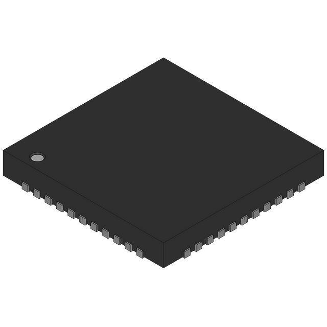
– 44-lead TQFP, and 44-pad QFN/MLF
Operating Voltages
– 2.7 - 5.5V for ATmega164P/324P/644P
Speed Grades
– ATmega164P/324P/644P: 0 - 8MHz @ 2.7 - 5.5V, 0 - 16MHz @ 4.5 - 5.5V
Power Consumption at 8 MHz, 5V, 25⋅C for ATmega644P
– Active mode: 8 mA
– Idle mode: 2.4 mA
– Power-down Mode: 0.8 µA
Notes:
8-bit
Microcontroller
with 16/32/64K
Bytes In-System
Programmable
Flash
ATmega164P
ATmega324P
ATmega644P
Automotive
Summary
1. Differential Mode is not recommended above 85°C.
7674DS–AVR–08/08
�1. Pin Configurations
Figure 1-1.
Pinout ATmega164P/324P/644P
PB4 (SS/OC0B/PCINT12)
PB3 (AIN1/OC0A/PCINT11)
PB2 (AIN0/INT2/PCINT10)
PB1 (T1/CLKO/PCINT9)
PB0 (XCK0/T0/PCINT8)
GND
VCC
PA0 (ADC0/PCINT0)
PA1 (ADC1/PCINT1)
PA2 (ADC2/PCINT2)
PA3 (ADC3/PCINT3)
TQFP/QFN/MLF
(PCINT13/MOSI) PB5
(PCINT14/MISO) PB6
(PCINT15/SCK) PB7
RESET
VCC
GND
XTAL2
XTAL1
(PCINT24/RXD0) PD0
(PCINT25/TXD0) PD1
NT/RXD1/26/INT0) PD2
(PCINT/TXD1/27/INT1)
(PCINT28/XCK1/OC1B)
(PCINT29/OC1A)
(PCINT30/OC2B/ICP)
(PCINT31/OC2A)
PD3
PD4
PD5
PD6
PD7
VCC
GND
(PCINT16/SCL) PC0
(PCINT17/SDA) PC1
(PCINT18/TCK) PC2
(PCINT19/TMS) PC3
PA4 (ADC4/PCINT
PA5 (ADC5/PCINT
PA6 (ADC6/PCINT
PA7 (ADC7/PCINT
AREF
GND
AVCC
PC7 (TOSC2/PCIN
PC6 (TOSC1/PCIN
PC5 (TDI/PCINT2
PC4 (TDO/PCINT2
Note:
2
The large center pad underneath the QFN/MLF package should be soldered to ground on the
board to ensure good mechanical stability.
ATmega164P/324P/644P
7674DS–AVR–08/08
�ATmega164P/324P/644P
2. Overview
The ATmega164P/324P/644P is a low-power CMOS 8-bit microcontroller based on the AVR
enhanced RISC architecture. By executing powerful instructions in a single clock cycle, the
ATmega164P/324P/644P achieves throughputs approaching 1 MIPS per MHz allowing the system designer to optimize power consumption versus processing speed.
2.1
Block Diagram
Figure 2-1.
Block Diagram
PA7..0
PB7..0
VCC
RESET
GND
Power
Supervision
POR / BOD &
RESET
PORT A (8)
PORT B (8)
Watchdog
Timer
Analog
Comparator
A/D
Converter
Watchdog
Oscillator
USART 0
XTAL1
Oscillator
Circuits /
Clock
Generation
EEPROM
Internal
Bandgap reference
SPI
XTAL2
8bit T/C 0
CPU
JTAG/OCD
TWI
PORT C (8)
TOSC2/PC7
TOSC1/PC6
PC5..0
16bit T/C 1
FLASH
SRAM
8bit T/C 2
USART 1
PORT D (8)
PD7..0
The AVR core combines a rich instruction set with 32 general purpose working registers. All the
32 registers are directly connected to the Arithmetic Logic Unit (ALU), allowing two independent
registers to be accessed in one single instruction executed in one clock cycle. The resulting
architecture is more code efficient while achieving throughputs up to ten times faster than conventional CISC microcontrollers.
3
7674DS–AVR–08/08
�The ATmega164P/324P/644P provides the following features: 16/32/64K bytes of In-System
Programmable Flash with Read-While-Write capabilities, 512B/1K/2K bytes EEPROM, 1/2/4K
bytes SRAM, 32 general purpose I/O lines, 32 general purpose working registers, Real Time
Counter (RTC), three flexible Timer/Counters with compare modes and PWM, 2 USARTs, a byte
oriented 2-wire Serial Interface, a 8-channel, 10-bit ADC with optional differential input stage
with programmable gain, programmable Watchdog Timer with Internal Oscillator, an SPI serial
port, IEEE std. 1149.1 compliant JTAG test interface, also used for accessing the On-chip
Debug system and programming and six software selectable power saving modes. The Idle
mode stops the CPU while allowing the SRAM, Timer/Counters, SPI port, and interrupt system
to continue functioning. The Power-down mode saves the register contents but freezes the
Oscillator, disabling all other chip functions until the next interrupt or Hardware Reset. In Powersave mode, the asynchronous timer continues to run, allowing the user to maintain a timer base
while the rest of the device is sleeping. The ADC Noise Reduction mode stops the CPU and all
I/O modules except Asynchronous Timer and ADC, to minimize switching noise during ADC
conversions. In Standby mode, the Crystal/Resonator Oscillator is running while the rest of the
device is sleeping. This allows very fast start-up combined with low power consumption. In
Extended Standby mode, both the main Oscillator and the Asynchronous Timer continue to run.
The device is manufactured using Atmel’s high-density nonvolatile memory technology. The Onchip ISP Flash allows the program memory to be reprogrammed in-system through an SPI serial
interface, by a conventional nonvolatile memory programmer, or by an On-chip Boot program
running on the AVR core. The boot program can use any interface to download the application
program in the application Flash memory. Software in the Boot Flash section will continue to run
while the Application Flash section is updated, providing true Read-While-Write operation. By
combining an 8-bit RISC CPU with In-System Self-Programmable Flash on a monolithic chip,
the Atmel ATmega164P/324P/644P is a powerful microcontroller that provides a highly flexible
and cost effective solution to many embedded control applications.
The ATmega164P/324P/644P AVR is supported with a full suite of program and system development tools including: C compilers, macro assemblers, program debugger/simulators, in-circuit
emulators, and evaluation kits.
2.2
Comparison Between ATmega164P, ATmega324P and ATmega644P
Table 2-1.
Automotive
Quality Grade
4
Differences between ATmega164P and ATmega644P
Device
Flash
EEPROM
RAM
ATmega164P
16 Kbyte
512 Bytes
1 Kbyte
ATmega324P
32 Kbyte
1 Kbyte
2 Kbyte
ATmega644P
64 Kbyte
2 Kbyte
4 Kbyte
The ATmega164P/324P/644P have been developed and manufactured according to the most
stringent requirements of the international standard ISO-TS-16949. This data sheet contains
limit values extracted from the results of extensive characterization (Temperature and Voltage).
The quality and reliability of the ATmega164P/324P/644P have been verified during regular
product qualification as per AEC-Q100 grade 1.
ATmega164P/324P/644P
7674DS–AVR–08/08
�ATmega164P/324P/644P
As indicated in the ordering information paragraph, the products are available in three different
temperature grades, but with equivalent quality and reliability objectives. Different temperature
identifiers have been defined as listed in Table 1.
Table 1. Temperature Grade Identification for Automotive Products
Temperature
Temperature
Identifier
Comments
-40 ; +85
T
Similar to Industrial Temperature Grade but with
Automotive Quality
-40 ; +105
T1
Reduced Automotive Temperature Range
-40 ; +125
Z
Full AutomotiveTemperature Range
5
7674DS–AVR–08/08
�3. Register Summary
Address
(0xFF)
6
Bit 7
Bit 6
Bit 5
Bit 4
Reserved
Name
-
-
-
-
Bit 3
Bit 2
Bit 1
Bit 0
-
-
-
(0xFE)
Reserved
-
-
-
-
-
-
-
-
(0xFD)
Reserved
-
-
-
-
-
-
-
-
(0xFC)
Reserved
-
-
-
-
-
-
-
-
(0xFB)
Reserved
-
-
-
-
-
-
-
(0xFA)
Reserved
-
-
-
-
-
-
-
(0xF9)
Reserved
-
-
-
-
-
-
-
(0xF8)
Reserved
-
-
-
-
-
-
-
-
(0xF7)
Reserved
-
-
-
-
-
-
-
-
(0xF6)
Reserved
-
-
-
-
-
-
-
-
(0xF5)
Reserved
-
-
-
-
-
-
-
(0xF4)
Reserved
-
-
-
-
-
-
-
-
(0xF3)
Reserved
-
-
-
-
-
-
-
-
(0xF2)
Reserved
-
-
-
-
-
-
-
-
(0xF1)
Reserved
-
-
-
-
-
-
-
(0xF0)
Reserved
-
-
-
-
-
-
-
(0xEF)
Reserved
-
-
-
-
-
-
-
(0xEE)
Reserved
-
-
-
-
-
-
-
-
(0xED)
Reserved
-
-
-
-
-
-
-
-
(0xEC)
Reserved
-
-
-
-
-
-
-
-
(0xEB)
Reserved
-
-
-
-
-
-
-
(0xEA)
Reserved
-
-
-
-
-
-
-
-
(0xE9)
Reserved
-
-
-
-
-
-
-
-
(0xE8)
Reserved
-
-
-
-
-
-
-
-
(0xE7)
Reserved
-
-
-
-
-
-
-
(0xE6)
Reserved
-
-
-
-
-
-
-
-
(0xE5)
Reserved
-
-
-
-
-
-
-
-
(0xE4)
Reserved
-
-
-
-
-
-
-
-
(0xE3)
Reserved
-
-
-
-
-
-
-
(0xE2)
Reserved
-
-
-
-
-
-
-
(0xE1)
Reserved
-
-
-
-
-
-
-
(0xE0)
Reserved
-
-
-
-
-
-
-
(0xDF)
Reserved
-
-
-
-
-
-
-
-
(0xDE)
Reserved
-
-
-
-
-
-
-
-
(0xDD)
Reserved
-
-
-
-
-
-
-
-
(0xDC)
Reserved
-
-
-
-
-
-
-
(0xDB)
Reserved
-
-
-
-
-
-
-
-
(0xDA)
Reserved
-
-
-
-
-
-
-
-
(0xD9)
Reserved
-
-
-
-
-
-
-
-
(0xD8)
Reserved
-
-
-
-
-
-
-
-
(0xD7)
Reserved
-
-
-
-
-
-
-
-
(0xD6)
Reserved
-
-
-
-
-
-
-
-
(0xD5)
Reserved
-
-
-
-
-
-
-
-
(0xD4)
Reserved
-
-
-
-
-
-
-
-
(0xD3)
Reserved
-
-
-
-
-
-
-
-
(0xD2)
Reserved
-
-
-
-
-
-
-
-
(0xD1)
Reserved
-
-
-
-
-
-
-
-
(0xD0)
Reserved
-
-
-
-
-
-
-
-
(0xCF)
Reserved
-
-
-
-
-
-
-
-
(0xCE)
UDR1
(0xCD)
UBRR1H
(0xCC)
UBRR1L
(0xCB)
-
-
-
USART1 I/O Data Register
188
-
-
-
Reserved
-
-
-
-
-
-
-
-
(0xCA)
UCSR1C
UMSEL11
UMSEL10
UPM11
UPM10
USBS1
UCSZ11
UCSZ10
UCPOL1
(0xC9)
UCSR1B
RXCIE1
TXCIE1
UDRIE1
RXEN1
TXEN1
UCSZ12
RXB81
TXB81
189/203
(0xC8)
UCSR1A
RXC1
TXC1
UDRE1
FE1
DOR1
UPE1
U2X1
MPCM1
188/203
-
-
-
-
-
-
-
-
(0xC7)
Reserved
(0xC6)
UDR0
(0xC5)
UBRR0H
(0xC4)
UBRR0L
(0xC3)
-
Page
USART1 Baud Rate Register High Byte
192/205
USART1 Baud Rate Register Low Byte
192/205
USART0 I/O Data Register
-
190/204
188
-
-
-
USART0 Baud Rate Register High Byte
192/205
Reserved
-
-
-
-
-
-
-
-
(0xC2)
UCSR0C
UMSEL01
UMSEL00
UPM01
UPM00
USBS0
UCSZ01
UCSZ00
UCPOL0
(0xC1)
UCSR0B
RXCIE0
TXCIE0
UDRIE0
RXEN0
TXEN0
UCSZ02
RXB80
TXB80
189/203
(0xC0)
UCSR0A
RXC0
TXC0
UDRE0
FE0
DOR0
UPE0
U2X0
MPCM0
188/203
USART0 Baud Rate Register Low Byte
192/205
190/204
ATmega164P/324P/644P
7674DS–AVR–08/08
�ATmega164P/324P/644P
Address
(0xBF)
Name
Reserved
Bit 7
Bit 6
Bit 5
Bit 4
Bit 3
Bit 2
Bit 1
Bit 0
-
-
-
-
-
-
-
-
(0xBE)
Reserved
-
-
-
-
-
-
-
(0xBD)
TWAMR
TWAM6
TWAM5
TWAM4
TWAM3
TWAM2
TWAM1
TWAM0
-
(0xBC)
TWCR
TWINT
TWEA
TWSTA
TWSTO
TWWC
TWEN
-
TWIE
(0xBB)
TWDR
2-wire Serial Interface Data Register
Page
234
231
233
(0xBA)
TWAR
TWA6
TWA5
TWA4
TWA3
TWA2
TWA1
TWA0
TWGCE
234
(0xB9)
TWSR
TWS7
TWS6
TWS5
TWS4
TWS3
-
TWPS1
TWPS0
233
(0xB8)
TWBR
(0xB7)
Reserved
-
-
-
2-wire Serial Interface Bit Rate Register
-
-
-
-
-
231
(0xB6)
ASSR
-
EXCLK
AS2
TCN2UB
OCR2AUB
OCR2BUB
TCR2AUB
TCR2BUB
(0xB5)
Reserved
-
-
-
-
-
-
-
-
(0xB4)
OCR2B
Timer/Counter2 Output Compare Register B
(0xB3)
OCR2A
Timer/Counter2 Output Compare Register A
157
(0xB2)
TCNT2
Timer/Counter2 (8 Bit)
156
157
157
(0xB1)
TCCR2B
FOC2A
FOC2B
-
-
WGM22
CS22
CS21
CS20
155
(0xB0)
TCCR2A
COM2A1
COM2A0
COM2B1
COM2B0
-
-
WGM21
WGM20
152
(0xAF)
Reserved
-
-
-
-
-
-
-
-
(0xAE)
Reserved
-
-
-
-
-
-
-
-
(0xAD)
Reserved
-
-
-
-
-
-
-
-
(0xAC)
Reserved
-
-
-
-
-
-
-
-
(0xAB)
Reserved
-
-
-
-
-
-
-
-
(0xAA)
Reserved
-
-
-
-
-
-
-
-
(0xA9)
Reserved
-
-
-
-
-
-
-
-
(0xA8)
Reserved
-
-
-
-
-
-
-
-
(0xA7)
Reserved
-
-
-
-
-
-
-
-
(0xA6)
Reserved
-
-
-
-
-
-
-
-
(0xA5)
Reserved
-
-
-
-
-
-
-
-
(0xA4)
Reserved
-
-
-
-
-
-
-
-
(0xA3)
Reserved
-
-
-
-
-
-
-
-
(0xA2)
Reserved
-
-
-
-
-
-
-
-
(0xA1)
Reserved
-
-
-
-
-
-
-
-
(0xA0)
Reserved
-
-
-
-
-
-
-
-
(0x9F)
Reserved
-
-
-
-
-
-
-
-
(0x9E)
Reserved
-
-
-
-
-
-
-
-
(0x9D)
Reserved
-
-
-
-
-
-
-
-
(0x9C)
Reserved
-
-
-
-
-
-
-
-
(0x9B)
Reserved
-
-
-
-
-
-
-
-
(0x9A)
Reserved
-
-
-
-
-
-
-
-
(0x99)
Reserved
-
-
-
-
-
-
-
-
(0x98)
Reserved
-
-
-
-
-
-
-
-
(0x97)
Reserved
-
-
-
-
-
-
-
-
(0x96)
Reserved
-
-
-
-
-
-
-
-
(0x95)
Reserved
-
-
-
-
-
-
-
-
(0x94)
Reserved
-
-
-
-
-
-
-
-
(0x93)
Reserved
-
-
-
-
-
-
-
-
(0x92)
Reserved
-
-
-
-
-
-
-
-
(0x91)
Reserved
-
-
-
-
-
-
-
-
(0x90)
Reserved
-
-
-
-
-
-
-
-
(0x8F)
Reserved
-
-
-
-
-
-
-
-
(0x8E)
Reserved
-
-
-
-
-
-
-
-
(0x8D)
Reserved
-
-
-
-
-
-
-
-
(0x8C)
Reserved
-
-
-
-
-
-
-
-
(0x8B)
OCR1BH
Timer/Counter1 - Output Compare Register B High Byte
(0x8A)
OCR1BL
Timer/Counter1 - Output Compare Register B Low Byte
136
(0x89)
OCR1AH
Timer/Counter1 - Output Compare Register A High Byte
136
(0x88)
OCR1AL
Timer/Counter1 - Output Compare Register A Low Byte
136
(0x87)
ICR1H
Timer/Counter1 - Input Capture Register High Byte
137
(0x86)
ICR1L
Timer/Counter1 - Input Capture Register Low Byte
137
(0x85)
TCNT1H
Timer/Counter1 - Counter Register High Byte
136
136
(0x84)
TCNT1L
(0x83)
Reserved
-
-
-
Timer/Counter1 - Counter Register Low Byte
(0x82)
TCCR1C
FOC1A
FOC1B
-
-
-
-
-
-
135
(0x81)
TCCR1B
ICNC1
ICES1
-
WGM13
WGM12
CS12
CS11
CS10
134
-
-
136
-
-
-
(0x80)
TCCR1A
COM1A1
COM1A0
COM1B1
COM1B0
-
-
WGM11
WGM10
132
(0x7F)
DIDR1
-
-
-
-
-
-
AIN1D
AIN0D
238
(0x7E)
DIDR0
ADC7D
ADC6D
ADC5D
ADC4D
ADC3D
ADC2D
ADC1D
ADC0D
258
7
7674DS–AVR–08/08
�Address
(0x7D)
8
Name
Reserved
Bit 7
Bit 6
Bit 5
Bit 4
Bit 3
Bit 2
Bit 1
Bit 0
-
-
-
-
-
-
-
-
Page
(0x7C)
ADMUX
REFS1
REFS0
ADLAR
MUX4
MUX3
MUX2
MUX1
MUX0
(0x7B)
ADCSRB
-
ACME
-
-
-
ADTS2
ADTS1
ADTS0
237
(0x7A)
ADCSRA
ADEN
ADSC
ADATE
ADIF
ADIE
ADPS2
ADPS1
ADPS0
256
(0x79)
ADCH
ADC Data Register High byte
(0x78)
ADCL
ADC Data Register Low byte
(0x77)
Reserved
-
-
-
-
-
-
-
-
(0x76)
Reserved
-
-
-
-
-
-
-
-
(0x75)
Reserved
-
-
-
-
-
-
-
-
(0x74)
Reserved
-
-
-
-
-
-
-
-
(0x73)
PCMSK3
PCINT31
PCINT30
PCINT29
PCINT28
PCINT27
PCINT26
PCINT25
PCINT24
(0x72)
Reserved
-
-
-
-
-
-
-
-
(0x71)
Reserved
-
-
-
-
-
-
-
-
(0x70)
TIMSK2
-
-
-
-
-
OCIE2B
OCIE2A
TOIE2
158
(0x6F)
TIMSK1
-
-
ICIE1
-
-
OCIE1B
OCIE1A
TOIE1
137
(0x6E)
TIMSK0
-
-
-
-
-
OCIE0B
OCIE0A
TOIE0
109
(0x6D)
PCMSK2
PCINT23
PCINT22
PCINT21
PCINT20
PCINT19
PCINT18
PCINT17
PCINT16
70
(0x6C)
PCMSK1
PCINT15
PCINT14
PCINT13
PCINT12
PCINT11
PCINT10
PCINT9
PCINT8
70
(0x6B)
PCMSK0
PCINT7
PCINT6
PCINT5
PCINT4
PCINT3
PCINT2
PCINT1
PCINT0
71
(0x6A)
Reserved
-
-
-
-
-
-
-
-
(0x69)
EICRA
-
-
ISC21
ISC20
ISC11
ISC10
ISC01
ISC00
67
(0x68)
PCICR
-
-
-
-
PCIE3
PCIE2
PCIE1
PCIE0
69
(0x67)
Reserved
-
-
-
-
-
-
-
-
-
-
-
-
-
-
-
-
PRTWI
PRTIM2
PRTIM0
PRUSART1
PRTIM1
PRSPI
PRUSART0
PRADC
-
-
-
-
-
-
-
-
(0x66)
OSCCAL
(0x65)
Reserved
(0x64)
PRR
(0x63)
Reserved
(0x62)
Reserved
(0x61)
CLKPR
(0x60)
WDTCSR
254
257
257
Oscillator Calibration Register
70
40
48
-
-
-
-
-
-
-
-
CLKPCE
-
-
-
CLKPS3
CLKPS2
CLKPS1
CLKPS0
40
WDIF
WDIE
WDP3
WDCE
WDE
WDP2
WDP1
WDP0
60
0x3F (0x5F)
SREG
I
T
H
S
V
N
Z
C
10
0x3E (0x5E)
SPH
SP15
SP14
SP13
SP12
SP11
SP10
SP9
SP8
11
0x3D (0x5D)
SPL
SP7
SP6
SP5
SP4
SP3
SP2
SP1
SP0
11
0x3C (0x5C)
Reserved
-
-
-
-
-
-
-
-
0x3B (0x5B)
Reserved
-
-
-
-
-
-
-
-
0x3A (0x5A)
Reserved
-
-
-
-
-
-
-
-
0x39 (0x59)
Reserved
-
-
-
-
-
-
-
-
0x38 (0x58)
Reserved
-
-
-
-
-
-
-
-
0x37 (0x57)
SPMCSR
SPMIE
RWWSB
SIGRD
RWWSRE
BLBSET
PGWRT
PGERS
SPMEN
0x36 (0x56)
Reserved
-
-
-
-
-
-
-
-
0x35 (0x55)
MCUCR
JTD
BODS
BODSE
PUD
-
-
IVSEL
IVCE
91/274
0x34 (0x54)
MCUSR
-
-
-
JTRF
WDRF
BORF
EXTRF
PORF
59/274
0x33 (0x53)
SMCR
-
-
-
-
SM2
SM1
SM0
SE
47
0x32 (0x52)
Reserved
-
-
-
-
-
-
-
-
0x31 (0x51)
OCDR
0x30 (0x50)
ACSR
ACD
ACBG
ACO
ACI
ACIE
ACIC
ACIS1
ACIS0
-
-
-
-
-
-
-
-
On-Chip Debug Register
290
264
256
0x2F (0x4F)
Reserved
0x2E (0x4E)
SPDR
0x2D (0x4D)
SPSR
SPIF0
WCOL0
-
0x2C (0x4C)
SPCR
SPIE0
SPE0
DORD0
0x2B (0x4B)
GPIOR2
General Purpose I/O Register 2
0x2A (0x4A)
GPIOR1
General Purpose I/O Register 1
0x29 (0x49)
Reserved
0x28 (0x48)
OCR0B
Timer/Counter0 Output Compare Register B
0x27 (0x47)
OCR0A
Timer/Counter0 Output Compare Register A
108
0x26 (0x46)
TCNT0
Timer/Counter0 (8 Bit)
108
SPI 0 Data Register
-
-
169
-
-
-
-
SPI2X0
168
MSTR0
CPOL0
CPHA0
SPR01
SPR00
167
-
-
28
28
-
-
-
109
0x25 (0x45)
TCCR0B
FOC0A
FOC0B
-
-
WGM02
CS02
CS01
CS00
0x24 (0x44)
TCCR0A
COM0A1
COM0A0
COM0B1
COM0B0
-
-
WGM01
WGM00
109
0x23 (0x43)
GTCCR
TSM
-
-
-
-
-
PSR2
PSR54310
159
0x22 (0x42)
EEARH
-
-
-
0x21 (0x41)
EEARL
-
EEPROM Address Register High Byte
107
23
EEPROM Address Register Low Byte
23
0x20 (0x40)
EEDR
0x1F (0x3F)
EECR
EEPROM Data Register
0x1E (0x3E)
GPIOR0
0x1D (0x3D)
EIMSK
-
-
-
-
-
INT2
INT1
INT0
68
0x1C (0x3C)
EIFR
-
-
-
-
-
INTF2
INTF1
INTF0
68
-
-
EEPM1
EEPM0
EERIE
23
EEMWE
EEWE
EERE
General Purpose I/O Register 0
23
28
ATmega164P/324P/644P
7674DS–AVR–08/08
�ATmega164P/324P/644P
Bit 7
Bit 6
Bit 5
Bit 4
Bit 3
Bit 2
Bit 1
Bit 0
Page
0x1B (0x3B)
Address
PCIFR
Name
-
-
-
-
PCIF3
PCIF2
PCIF1
PCIF0
69
0x1A (0x3A)
Reserved
-
-
-
-
-
-
-
-
0x19 (0x39)
Reserved
-
-
-
-
-
-
-
-
0x18 (0x38)
Reserved
-
-
-
-
-
-
-
-
0x17 (0x37)
TIFR2
-
-
-
-
-
OCF2b
OCF2A
TOV2
159
0x16 (0x36)
TIFR1
-
-
ICF1
-
-
OCF1B
OCF1A
TOV1
138
0x15 (0x35)
TIFR0
-
-
-
-
-
OCF0B
OCF0A
TOV0
109
0x14 (0x34)
Reserved
-
-
-
-
-
-
-
-
0x13 (0x33)
Reserved
-
-
-
-
-
-
-
-
0x12 (0x32)
Reserved
-
-
-
-
-
-
-
-
0x11 (0x31)
Reserved
-
-
-
-
-
-
-
-
0x10 (0x30)
Reserved
-
-
-
-
-
-
-
-
0x0F (0x2F)
Reserved
-
-
-
-
-
-
-
-
0x0E (0x2E)
Reserved
-
-
-
-
-
-
-
-
0x0D (0x2D)
Reserved
-
-
-
-
-
-
-
-
0x0C (0x2C)
Reserved
-
-
-
-
-
-
-
-
0x0B (0x2B)
PORTD
PORTD7
PORTD6
PORTD5
PORTD4
PORTD3
PORTD2
PORTD1
PORTD0
92
0x0A (0x2A)
DDRD
DDD7
DDD6
DDD5
DDD4
DDD3
DDD2
DDD1
DDD0
92
92
0x09 (0x29)
PIND
PIND7
PIND6
PIND5
PIND4
PIND3
PIND2
PIND1
PIND0
0x08 (0x28)
PORTC
PORTC7
PORTC6
PORTC5
PORTC4
PORTC3
PORTC2
PORTC1
PORTC0
92
0x07 (0x27)
DDRC
DDC7
DDC6
DDC5
DDC4
DDC3
DDC2
DDC1
DDC0
92
92
0x06 (0x26)
PINC
PINC7
PINC6
PINC5
PINC4
PINC3
PINC2
PINC1
PINC0
0x05 (0x25)
PORTB
PORTB7
PORTB6
PORTB5
PORTB4
PORTB3
PORTB2
PORTB1
PORTB0
91
0x04 (0x24)
DDRB
DDB7
DDB6
DDB5
DDB4
DDB3
DDB2
DDB1
DDB0
91
0x03 (0x23)
PINB
0x02 (0x22)
PORTA
PINB7
PINB6
PINB5
PINB4
PINB3
PINB2
PINB1
PINB0
91
PORTA7
PORTA6
PORTA5
PORTA4
PORTA3
PORTA2
PORTA1
PORTA0
91
0x01 (0x21)
DDRA
DDA7
DDA6
DDA5
DDA4
DDA3
DDA2
DDA1
DDA0
91
0x00 (0x20)
PINA
PINA7
PINA6
PINA5
PINA4
PINA3
PINA2
PINA1
PINA0
91
Notes:
1. For compatibility with future devices, reserved bits should be written to zero if accessed. Reserved I/O memory addresses
should never be written.
2. I/O registers within the address range $00 - $1F are directly bit-accessible using the SBI and CBI instructions. In these registers, the value of single bits can be checked by using the SBIS and SBIC instructions.
3. Some of the status flags are cleared by writing a logical one to them. Note that the CBI and SBI instructions will operate on
all bits in the I/O register, writing a one back into any flag read as set, thus clearing the flag. The CBI and SBI instructions
work with registers 0x00 to 0x1F only.
4. When using the I/O specific commands IN and OUT, the I/O addresses $00 - $3F must be used. When addressing I/O registers as data space using LD and ST instructions, $20 must be added to these addresses. The ATmega164P/324P/644P is
a complex microcontroller with more peripheral units than can be supported within the 64 location reserved in Opcode for
the IN and OUT instructions. For the Extended I/O space from $60 - $FF, only the ST/STS/STD and LD/LDS/LDD instructions can be used.
9
7674DS–AVR–08/08
�4. Instruction Set Summary
Mnemonics
Operands
Description
Operation
Flags
#Clocks
ARITHMETIC AND LOGIC INSTRUCTIONS
ADD
Rd, Rr
Add two Registers
Rd ← Rd + Rr
Z,C,N,V,H
ADC
Rd, Rr
Add with Carry two Registers
Rd ← Rd + Rr + C
Z,C,N,V,H
1
ADIW
Rdl,K
Add Immediate to Word
Rdh:Rdl ← Rdh:Rdl + K
Z,C,N,V,S
2
SUB
Rd, Rr
Subtract two Registers
Rd ← Rd - Rr
Z,C,N,V,H
1
SUBI
Rd, K
Subtract Constant from Register
Rd ← Rd - K
Z,C,N,V,H
1
SBC
Rd, Rr
Subtract with Carry two Registers
Rd ← Rd - Rr - C
Z,C,N,V,H
1
1
SBCI
Rd, K
Subtract with Carry Constant from Reg.
Rd ← Rd - K - C
Z,C,N,V,H
1
SBIW
Rdl,K
Subtract Immediate from Word
Rdh:Rdl ← Rdh:Rdl - K
Z,C,N,V,S
2
1
AND
Rd, Rr
Logical AND Registers
Rd ← Rd • Rr
Z,N,V
ANDI
Rd, K
Logical AND Register and Constant
Rd ← Rd • K
Z,N,V
1
OR
Rd, Rr
Logical OR Registers
Rd ← Rd v Rr
Z,N,V
1
ORI
Rd, K
Logical OR Register and Constant
Rd ← Rd v K
Z,N,V
1
EOR
Rd, Rr
Exclusive OR Registers
Rd ← Rd ⊕ Rr
Z,N,V
1
COM
Rd
One’s Complement
Rd ← 0xFF − Rd
Z,C,N,V
1
NEG
Rd
Two’s Complement
Rd ← 0x00 − Rd
Z,C,N,V,H
1
SBR
Rd,K
Set Bit(s) in Register
Rd ← Rd v K
Z,N,V
1
CBR
Rd,K
Clear Bit(s) in Register
Rd ← Rd • (0xFF - K)
Z,N,V
1
INC
Rd
Increment
Rd ← Rd + 1
Z,N,V
1
DEC
Rd
Decrement
Rd ← Rd − 1
Z,N,V
1
TST
Rd
Test for Zero or Minus
Rd ← Rd • Rd
Z,N,V
1
CLR
Rd
Clear Register
Rd ← Rd ⊕ Rd
Z,N,V
1
SER
Rd
Set Register
Rd ← 0xFF
None
1
MUL
Rd, Rr
Multiply Unsigned
R1:R0 ← Rd x Rr
Z,C
2
MULS
Rd, Rr
Multiply Signed
R1:R0 ← Rd x Rr
Z,C
2
MULSU
Rd, Rr
Multiply Signed with Unsigned
R1:R0 ← Rd x Rr
Z,C
2
FMUL
Rd, Rr
Fractional Multiply Unsigned
R1:R0 ← (Rd x Rr)


 工商网监
湘ICP备2023018690号
工商网监
湘ICP备2023018690号
