Features
• High Performance, Low Power AVR® 8-bit Microcontroller
• Advanced RISC Architecture
•
•
•
•
•
•
•
•
•
•
– 131 Powerful Instructions - Most Single Clock Cycle Execution
– 32 x 8 General Purpose Working Registers
– Fully Static Operation
– Up to 4 MIPS Throughput at 4 MHz
High Endurance Non-volatile Memorie segments
– 8K/16K Bytes of In-System Self-Programmable Flash Program
Memory(ATmega8HVA/16HVA)
– 256 Bytes EEPROM
– 512 Bytes Internal SRAM
– Write/Erase cycles: 10,000 Flash/100,000 EEPROM
– Data Retention: 20 years at 85°C /100 years at 25°C(1)
– Programming Lock for Software Security
Battery Management Features
– One or Two Cells in Series
– Over-current Protection (Charge and Discharge)
– Short-circuit Protection (Discharge)
– High Voltage Outputs to Drive N-Channel Charge/Discharge FETs
Peripheral Features
– Two configurable 8- or 16-bit Timers with Separate Prescaler, Optional Input
Capture (IC), Compare Mode and CTC
– SPI - Serial Programmable Interface
– 12-bit Voltage ADC, Four External and One Internal ADC Inputs
– High Resolution Coulomb Counter ADC for Current Measurements
– Programmable Watchdog Timer
Special Microcontroller Features
– debugWIRE On-chip Debug System
– In-System Programmable via SPI ports
– Power-on Reset
– On-chip Voltage Regulator with Short-circuit Monitoring Interface
– External and Internal Interrupt Sources
– Sleep Modes:
Idle, ADC Noise Reduction, Power-save, and Power-off
Additional Secure Authentication Features available only under NDA
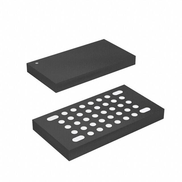
Packages
– 36-pad LGA
– 28-lead TSOP
Operating Voltage: 1.8 - 9V
Maximum Withstand Voltage (High-voltage pins): 28V
Temperature Range: - 20°C to 85°C
Speed Grade: 1-4 MHz
8-bit
Microcontroller
with 8K/16K
Bytes In-System
Programmable
Flash
ATmega8HVA
ATmega16HVA
Preliminary
8024A–AVR–04/08
�1. Pin Configurations
1.1
LGA
Figure 1-1.
LGA - Pinout ATmega8HVA/16HVA
1
2
3
4
5
6
7
8
A
B
C
D
E
Figure 1-2.
2
LGA - pinout ATmega8HVA/16HVA
1
2
3
4
5
6
7
8
A
DNC
PV2
PV1
NV
GND
OC
OD
DNC
B
CF2P
CF2N
VFET
CF1P
GND
PC0
DNC
GND
C
VREF
VREFGND
VREG
CF1N
VCC
GND
GND
BATT
D
PI
NI
GND
GND
GND
PB2
PB3
GND
E
DNC
DNC
PA1
PA0
PB1
PB0
RESET
DNC
ATmega8HVA/16HVA
8024A–AVR–04/08
�ATmega8HVA/16HVA
1.2
TSOP
Figure 1-3.
1.3
1.3.1
TSOP - pinout ATmega8HVA/16HVA
PV2
1
28
OD
PV1
2
27
OC
NV
3
26
GND
GND
4
25
BATT
VFET
5
24
PC0 (RXD/TXD/INT0)
CF1P
6
23
VCC
CF1N
7
22
GND
CF2P
8
21
PB3 (MISO/INT2)
CF2N
9
20
PB2 (MOSI/INT1)
VREG
10
19
PB1 (SCK)
VREF
11
18
PB0 (SS/CKOUT)
VREFGND
12
17
PA2 (RESET/dW)
PI
13
16
PA1 (ADC1/SGND/T1)
NI
14
15
PA0 (ADC0/SGND/T0)
Pin Descriptions
VFET
Input to the internal voltage regulator.
1.3.2
VCC
Digital supply voltage. Normally connected to VREG.
1.3.3
VREG
Output from the internal voltage regulator.
1.3.4
CF1P/CF1N/CF2P/CF2N
CF1P/CF1N/CF2P/CF2N are the connection pins for connecting external fly capacitors to the
step-up regulator.
1.3.5
VREF
Internal Voltage Reference for external decoupling.
1.3.6
VREFGND
Ground for decoupling of Internal Voltage Reference. Do not connect to GND or SGND on PCB.
3
8024A–AVR–04/08
�1.3.7
GND
Ground
1.3.8
Port A (PA1..PA0)
Port A serves as a low-voltage 2-bit bi-directional I/O port with internal pull-up resistors (selected
for each bit). As inputs, Port A pins that are externally pulled low will source current if the pull-up
resistors are activated. The Port A pins are tri-stated when a reset condition becomes active,
even if the clock is not running.
Port A also serves the functions of various special features of the ATmega8HVA/16HVA as
listed in ”Alternate Functions of Port A” on page 70.
1.3.9
Port B (PB3..PB0)
Port B is a low-voltage 4-bit bi-directional I/O port with internal pull-up resistors (selected for
each bit). As inputs, Port B pins that are externally pulled low will source current if the pull-up
resistors are activated. The Port B pins are tri-stated when a reset condition becomes active,
even if the clock is not running.
Port B also serves the functions of various special features of the ATmega8HVA/16HVA as
listed in ”Alternate Functions of Port B” on page 71.
1.3.10
PC0
Port C serves the functions of various special features of the ATmega8HVA/16HVA as listed in
”Alternate Functions of Port C” on page 61.
1.3.11
OC
High voltage output to drive Charge FET.
1.3.12
OD
High voltage output to drive Discharge FET.
1.3.13
NI
NI is the filtered negative input from the current sense resistor.
1.3.14
PI
PI is the filtered positive input from the current sense resistor.
1.3.15
NV/PV1/PV2
NV, PV1, and PV2 are the inputs for battery cells 1 and 2.
1.3.16
BATT
Input for detecting when a charger is connected.
1.3.17
RESET/dw
Reset input. A low level on this pin for longer than the minimum pulse length will generate a
reset, even if the clock is not running. The minimum pulse length is given in Table 11 on page
38. Shorter pulses are not guaranteed to generate a reset. This pin is also used as debugWIRE
communication pin.
4
ATmega8HVA/16HVA
8024A–AVR–04/08
�ATmega8HVA/16HVA
2. Overview
The ATmega8HVA/16HVA is a monitoring and protection circuit for 1-cell and 2-cell Li-ion applications with focus on high security/authentication, accurate monitoring, low cost and high
utilization of the cell energy. The device contains secure authentication features as well as
autonomous battery protection during charging and discharging. The chip allows very accurate
accumulated current measurements using an 18-bit ADC with a resolution of 0.84 µV. The feature set makes the ATmega8HVA/16HVA a key component in any system focusing on high
security, battery protection, accurate monitoring, high system utilization and low cost.
Figure 2-1.
Block Diagram
PB3..0
PC0
PB0
Oscillator
Circuits /
Clock
Generation
Oscillator
Sampling
Interface
Watchdog
Oscillator
VCC
PORTB (4)
SPI
Flash
Power
Supervision
POR &
RESET
8/16-bit T/C0
Battery
Protection
8/16-bit T/C1
Voltage
ADC
SRAM
VPTAT
EEPROM
CPU
GND
Charger
Detect
VFET
VREG
PV2
PV1
NV
debugWIRE
Security
Module
BATT
OC
OD
FET
Control
Program
Logic
Watchdog
Timer
RESET/dW
PORTC (1)
Voltage
Reference
Coulumb
Counter ADC
VREF
VREFGND
PI
NI
DATA BUS
Voltage Regulator
Monitor Interface
Voltage
Regulator
PORTA (2)
PA1..0
CF1N
CF2N
CF1P
PA1..0
CF2P
A combined step-up and linear voltage regulator ensures that the chip can operate with supply
voltages as low as 1.8V for 1-cell applications. The regulator automatically switches to linear
mode when the input voltage is sufficiently high, thereby ensuring a minimum power consumption at all times. For 2-cell applications, only linear regulation is enabled. The regulator
capabilities, combined with an extremely low power consumption in the power saving modes,
greatly enhances the cell energy utilization compared to existing solutions.
The chip utilizes Atmel's patented Deep Under-voltage Recovery (DUVR) mode that supports
pre-charging of deeply discharged battery cells without using a separate Pre-charge FET.
5
8024A–AVR–04/08
�The ATmega8HVA/16HVA contains a 12-bit ADC that can be used to measure the voltage of
each cell individually. The ADC can also be used to monitor temperature, either on-chip temperature using the built-in temperature sensor, external temperature using thermistors connected to
dedicated ADC inputs. The ATmega8HVA/16HVA contains a high-voltage tolerant, open-drain
IO pin that supports serial communication. Programming can be done in-system using the 4
General Purpose IO ports that support SPI programming.
The AVR core combines a rich instruction set with 32 general purpose working registers. All the
32 registers are directly connected to the Arithmetic Logic Unit (ALU), allowing two independent
registers to be accessed in one single instruction executed in one clock cycle. The resulting
architecture is more code efficient while achieving throughputs up to ten times faster than conventional CISC microcontrollers.
The MCU includes 8K/16K bytes of In-System Programmable Flash with Read-While-Write
capabilities, 256 bytes EEPROM, 512 bytes SRAM, 32 general purpose working registers, 6
general purpose I/O lines, debugWIRE for On-chip debugging and SPI for In-system Programming, two flexible Timer/Counters with Input Capture and compare modes, internal and external
interrupts, a 12-bit Sigma Delta ADC for voltage and temperature measurements, a high resolution Sigma Delta ADC for Coulomb Counting and instantaneous current measurements,
Additional Secure Authentication Features, an authonomous Battery Protection module, a programmable Watchdog Timer with wake-up capabilities, and software selectable power saving
modes.
The AVR core combines a rich instruction set with 32 general purpose working registers. All the
32 registers are directly connected to the Arithmetic Logic Unit (ALU), allowing two indepdent
registers to be accessed in one single instruction executed in one clock cycle. The resulting
architecture is more code efficient while achieving throughputs up to ten times faster than conventional CISC microcontrollers.
The device is manufactured using Atmel’s high voltage high density non-volatile memory technology. The On-chip ISP Flash allows the program memory to be reprogrammed In-System,
through an SPI serial interface, by a conventional non-volatile memory programmer or by an Onchip Boot program running on the AVR core. By combining an 8-bit RISC CPU with In-System
Self-Programmable Flash, fuel gauging ADCs, dedicated battery protection circuitry, and a voltage regulator on a monolithic chip, the ATmega8HVA/16HVA is a powerful microcontroller that
provides a highly flexible and cost effective solution for Li-ion Smart Battery applications.
The ATmega8HVA/16HVA AVR is supported with a full suite of program and system development tools including: C Compilers, Macro Assemblers, Program Debugger/Simulators, and Onchip Debugger.
The ATmega8HVA/16HVA is a low-power CMOS 8-bit microcontroller based on the AVR architecture. It is part of the AVR Smart Battery family that provides secure authentication, highly
accurate monitoring and autonomous protection for Lithium-ion battery cells.
6
ATmega8HVA/16HVA
8024A–AVR–04/08
�ATmega8HVA/16HVA
2.1
Comparison Between ATmega8HVA and ATmega16HVA
The ATmega8HVA and ATmega16HVA differ only in memory size and interrupt vector size.
Table 2-1 summarizes the different configuration for the two devices.
Table 2-1.
Configuration summary
Device
Flash
Interrupt vector size
ATmega8HVA
8K
1 Word
ATmega16HVA
16K
2 Word
3. Disclaimer
All Min, Typ and Max values contained in this datasheet are preliminary estimates based on simulations and characterization of other AVR microcontrollers manufactured on the same process
technology. Final values will be available after the device is characterized.
4. Resources
A comprehensive set of development tools, application notes and datasheets are available for
download on http://www.atmel.com/avr.
Note:
1.
5. Data Retention
Reliability Qualification results show that the projected data retention failure rate is much less
than 1 PPM over 20 years at 85°C or 100 years at 25°C.
6. About Code Examples
This documentation contains simple code examples that briefly show how to use various parts of
the device. These code examples assume that the part specific header file is included before
compilation. Be aware that not all C compiler vendors include bit definitions in the header files
and interrupt handling in C is compiler dependent. Please confirm with the C compiler documentation for more details.
For I/O registers located in extended I/O map, “IN”, “OUT”, “SBIS”, “SBIC”, “CBI”, and “SBI”
instructions must be replaced with instructions that allow access to extended I/O. Typically
“LDS” and “STS” combined with “SBRS”, “SBRC”, “SBR”, and “CBR”.
7
8024A–AVR–04/08
�7. AVR CPU Core
7.1
Overview
This section discusses the AVR core architecture in general. The main function of the CPU core
is to ensure correct program execution. The CPU must therefore be able to access memories,
perform calculations, control peripherals, and handle interrupts.
Figure 7-1.
Block Diagram of the AVR Architecture
Data Bus 8-bit
Flash
Program
Memory
Program
Counter
Status
and Control
32 x 8
General
Purpose
Registrers
Control Lines
Direct Addressing
Instruction
Decoder
Indirect Addressing
Instruction
Register
Interrupt
Unit
Watchdog
Timer
ALU
I/O Module1
I/O Module 2
Data
SRAM
I/O Module n
EEPROM
I/O Lines
In order to maximize performance and parallelism, the AVR uses a Harvard architecture – with
separate memories and buses for program and data. Instructions in the program memory are
executed with a single level pipelining. While one instruction is being executed, the next instruction is pre-fetched from the program memory. This concept enables instructions to be executed
in every clock cycle. The program memory is In-System Reprogrammable Flash memory.
The fast-access Register File contains 32 x 8-bit general purpose working registers with a single
clock cycle access time. This allows single-cycle Arithmetic Logic Unit (ALU) operation. In a typ-
8
ATmega8HVA/16HVA
8024A–AVR–04/08
�ATmega8HVA/16HVA
ical ALU operation, two operands are output from the Register File, the operation is executed,
and the result is stored back in the Register File – in one clock cycle.
Six of the 32 registers can be used as three 16-bit indirect address register pointers for Data
Space addressing – enabling efficient address calculations. One of the these address pointers
can also be used as an address pointer for look up tables in Flash program memory. These
added function registers are the 16-bit X-, Y-, and Z-register, described later in this section.
The ALU supports arithmetic and logic operations between registers or between a constant and
a register. Single register operations can also be executed in the ALU. After an arithmetic operation, the Status Register is updated to reflect information about the result of the operation.
Program flow is provided by conditional and unconditional jump and call instructions, able to
directly address the whole address space. Most AVR instructions have a single 16-bit word format. Every program memory address contains a 16- or 32-bit instruction.
During interrupts and subroutine calls, the return address Program Counter (PC) is stored on the
Stack. The Stack is effectively allocated in the general data SRAM, and consequently the Stack
size is only limited by the total SRAM size and the usage of the SRAM. All user programs must
initialize the SP in the Reset routine (before subroutines or interrupts are executed). The Stack
Pointer (SP) is read/write accessible in the I/O space. The data SRAM can easily be accessed
through the five different addressing modes supported in the AVR architecture.
The memory spaces in the AVR architecture are all linear and regular memory maps.
A flexible interrupt module has its control registers in the I/O space with an additional Global
Interrupt Enable bit in the Status Register. All interrupts have a separate Interrupt Vector in the
Interrupt Vector table. The interrupts have priority in accordance with their Interrupt Vector position. The lower the Interrupt Vector address, the higher the priority.
The I/O memory space contains 64 addresses for CPU peripheral functions as Control Registers, SPI, and other I/O functions. The I/O Memory can be accessed directly, or as the Data
Space locations following those of the Register File, 0x20 - 0x5F. In addition, the
ATmega8HVA/16HVA has Extended I/O space from 0x60 - 0xFF in SRAM where only the
ST/STS/STD and LD/LDS/LDD instructions can be used.
7.2
ALU – Arithmetic Logic Unit
The high-performance AVR ALU operates in direct connection with all the 32 general purpose
working registers. Within a single clock cycle, arithmetic operations between general purpose
registers or between a register and an immediate are executed. The ALU operations are divided
into three main categories – arithmetic, logical, and bit-functions. Some implementations of the
architecture also provide a powerful multiplier supporting both signed/unsigned multiplication
and fractional format. See the “Instruction Set” section for a detailed description.
7.3
Status Register
The Status Register contains information about the result of the most recently executed arithmetic instruction. This information can be used for altering program flow in order to perform
conditional operations. Note that the Status Register is updated after all ALU operations, as
specified in the Instruction Set Reference. This will in many cases remove the need for using the
dedicated compare instructions, resulting in faster and more compact code.
The Status Register is not automatically stored when entering an interrupt routine and restored
when returning from an interrupt. This must be handled by software.
9
8024A–AVR–04/08
�7.3.1
SREG – AVR Status Register
Bit
7
6
5
4
3
2
1
0
0x3F (0x5F)
I
T
H
S
V
N
Z
C
Read/Write
R/W
R/W
R/W
R/W
R/W
R/W
R/W
R/W
Initial Value
0
0
0
0
0
0
0
0
SREG
• Bit 7 – I: Global Interrupt Enable
The Global Interrupt Enable bit must be set for the interrupts to be enabled. The individual interrupt enable control is then performed in separate control registers. If the Global Interrupt Enable
Register is cleared, none of the interrupts are enabled independent of the individual interrupt
enable settings. The I-bit is cleared by hardware after an interrupt has occurred, and is set by
the RETI instruction to enable subsequent interrupts. The I-bit can also be set and cleared by
the application with the SEI and CLI instructions, as described in the instruction set reference.
• Bit 6 – T: Bit Copy Storage
The Bit Copy instructions BLD (Bit LoaD) and BST (Bit STore) use the T-bit as source or destination for the operated bit. A bit from a register in the Register File can be copied into T by the
BST instruction, and a bit in T can be copied into a bit in a register in the Register File by the
BLD instruction.
• Bit 5 – H: Half Carry Flag
The Half Carry Flag H indicates a Half Carry in some arithmetic operations. Half Carry Is useful
in BCD arithmetic. See the “Instruction Set Description” for detailed information.
• Bit 4 – S: Sign Bit, S = N ⊕ V
The S-bit is always an exclusive or between the negative flag N and the Two’s Complement
Overflow Flag V. See the “Instruction Set Description” for detailed information.
• Bit 3 – V: Two’s Complement Overflow Flag
The Two’s Complement Overflow Flag V supports two’s complement arithmetics. See the
“Instruction Set Description” for detailed information.
• Bit 2 – N: Negative Flag
The Negative Flag N indicates a negative result in an arithmetic or logic operation. See the
“Instruction Set Description” for detailed information.
• Bit 1 – Z: Zero Flag
The Zero Flag Z indicates a zero result in an arithmetic or logic operation. See the “Instruction
Set Description” for detailed information.
• Bit 0 – C: Carry Flag
The Carry Flag C indicates a carry in an arithmetic or logic operation. See the “Instruction Set
Description” for detailed information.
10
ATmega8HVA/16HVA
8024A–AVR–04/08
�ATmega8HVA/16HVA
7.4
General Purpose Register File
The Register File is optimized for the AVR Enhanced RISC instruction set. In order to achieve
the required performance and flexibility, the following input/output schemes are supported by the
Register File:
• One 8-bit output operand and one 8-bit result input
• Two 8-bit output operands and one 8-bit result input
• Two 8-bit output operands and one 16-bit result input
• One 16-bit output operand and one 16-bit result input
Figure 7-2 shows the structure of the 32 general purpose working registers in the CPU.
Figure 7-2.
AVR CPU General Purpose Working Registers
7
0
Addr.
R0
0x00
R1
0x01
R2
0x02
…
R13
0x0D
General
R14
0x0E
Purpose
R15
0x0F
Working
R16
0x10
Registers
R17
0x11
…
R26
0x1A
X-register Low Byte
R27
0x1B
X-register High Byte
R28
0x1C
Y-register Low Byte
R29
0x1D
Y-register High Byte
R30
0x1E
Z-register Low Byte
R31
0x1F
Z-register High Byte
Most of the instructions operating on the Register File have direct access to all registers, and
most of them are single cycle instructions.
As shown in Figure 7-2, each register is also assigned a data memory address, mapping them
directly into the first 32 locations of the user Data Space. Although not being physically implemented as SRAM locations, this memory organization provides great flexibility in access of the
registers, as the X-, Y- and Z-pointer registers can be set to index any register in the file.
7.4.1
The X-register, Y-register, and Z-register
The registers R26..R31 have some added functions to their general purpose usage. These registers are 16-bit address pointers for indirect addressing of the data space. The three indirect
address registers X, Y, and Z are defined as described in Figure 7-3 on page 12.
11
8024A–AVR–04/08
�Figure 7-3.
The X-, Y-, and Z-registers
15
X-register
XH
XL
7
0
R27 (0x1B)
YH
YL
7
0
R29 (0x1D)
Z-register
0
R26 (0x1A)
15
Y-register
0
7
0
7
0
R28 (0x1C)
15
ZH
7
0
ZL
7
R31 (0x1F)
0
0
R30 (0x1E)
In the different addressing modes these address registers have functions as fixed displacement,
automatic increment, and automatic decrement (see the instruction set reference for details).
7.5
Stack Pointer
The Stack is mainly used for storing temporary data, for storing local variables and for storing
return addresses after interrupts and subroutine calls. The Stack Pointer Register always points
to the top of the Stack. Note that the Stack is implemented as growing from higher memory locations to lower memory locations. This implies that a Stack PUSH command decreases the Stack
Pointer.
The Stack Pointer points to the data SRAM Stack area where the Subroutine and Interrupt
Stacks are located. This Stack space in the data SRAM must be defined by the program before
any subroutine calls are executed or interrupts are enabled. The Stack Pointer must be set to
point above 0x100. The Stack Pointer is decremented by one when data is pushed onto the
Stack with the PUSH instruction, and it is decremented by two when the return address is
pushed onto the Stack with subroutine call or interrupt. The Stack Pointer is incremented by one
when data is popped from the Stack with the POP instruction, and it is incremented by two when
data is popped from the Stack with return from subroutine RET or return from interrupt RETI.
The AVR Stack Pointer is implemented as two 8-bit registers in the I/O space. The number of
bits actually used is implementation dependent. Note that the data space in some implementations of the AVR architecture is so small that only SPL is needed. In this case, the SPH Register
will not be present.
7.5.1
SPH and SPL – Stack Pointer High and Stack Pointer Low
Bit
15
14
13
12
11
10
9
8
0x3E (0x5E)
SP15
SP14
SP13
SP12
SP11
SP10
SP9
SP8
SPH
0x3D (0x5D)
SP7
SP6
SP5
SP4
SP3
SP2
SP1
SP0
SPL
7
6
5
4
3
2
1
0
R/W
R/W
R/W
R/W
R/W
R/W
R/W
R/W
R/W
R/W
R/W
R/W
R/W
R/W
R/W
R/W
0
0
0
0
0
0
0
0
0
0
0
0
0
0
0
0
Read/Write
Initial Value
12
ATmega8HVA/16HVA
8024A–AVR–04/08
�ATmega8HVA/16HVA
7.6
Instruction Execution Timing
This section describes the general access timing concepts for instruction execution. The AVR
CPU is driven by the CPU clock clkCPU, directly generated from the selected clock source for the
chip. No internal clock division is used.
Figure 7-4 shows the parallel instruction fetches and instruction executions enabled by the Harvard architecture and the fast-access Register File concept. This is the basic pipelining concept
to obtain up to 1 MIPS per MHz with the corresponding unique results for functions per cost,
functions per clocks, and functions per power-unit.
Figure 7-4.
The Parallel Instruction Fetches and Instruction Executions
T1
T2
T3
T4
clkCPU
1st Instruction Fetch
1st Instruction Execute
2nd Instruction Fetch
2nd Instruction Execute
3rd Instruction Fetch
3rd Instruction Execute
4th Instruction Fetch
Figure 7-5 shows the internal timing concept for the Register File. In a single clock cycle an ALU
operation using two register operands is executed, and the result is stored back to the destination register.
Figure 7-5.
Single Cycle ALU Operation
T1
T2
T3
T4
clkCPU
Total Execution Time
Register Operands Fetch
ALU Operation Execute
Result Write Back
7.7
Reset and Interrupt Handling
The AVR provides several different interrupt sources. These interrupts and the separate Reset
Vector each have a separate program vector in the program memory space. All interrupts are
assigned individual enable bits which must be written logic one together with the Global Interrupt
Enable bit in the Status Register in order to enable the interrupt.
The lowest addresses in the program memory space are by default defined as the Reset and
Interrupt Vectors. The complete list of vectors is shown in ”Interrupts” on page 52. The list also
determines the priority levels of the different interrupts. The lower the address the higher is the
priority level. RESET has the highest priority.
13
8024A–AVR–04/08
�When an interrupt occurs, the Global Interrupt Enable I-bit is cleared and all interrupts are disabled. The user software can write logic one to the I-bit to enable nested interrupts. All enabled
interrupts can then interrupt the current interrupt routine. The I-bit is automatically set when a
Return from Interrupt instruction – RETI – is executed.
There are basically two types of interrupts. The first type is triggered by an event that sets the
interrupt flag. For these interrupts, the Program Counter is vectored to the actual Interrupt Vector
in order to execute the interrupt handling routine, and hardware clears the corresponding interrupt flag. Interrupt flags can also be cleared by writing a logic one to the flag bit position(s) to be
cleared. If an interrupt condition occurs while the corresponding interrupt enable bit is cleared,
the interrupt flag will be set and remembered until the interrupt is enabled, or the flag is cleared
by software. Similarly, if one or more interrupt conditions occur while the Global Interrupt Enable
bit is cleared, the corresponding interrupt flag(s) will be set and remembered until the Global
Interrupt Enable bit is set, and will then be executed by order of priority.
The second type of interrupts will trigger as long as the interrupt condition is present. These
interrupts do not necessarily have interrupt flags. If the interrupt condition disappears before the
interrupt is enabled, the interrupt will not be triggered.
When the AVR exits from an interrupt, it will always return to the main program and execute one
more instruction before any pending interrupt is served.
Note that the Status Register is not automatically stored when entering an interrupt routine, nor
restored when returning from an interrupt routine. This must be handled by software.
When using the CLI instruction to disable interrupts, the interrupts will be immediately disabled.
No interrupt will be executed after the CLI instruction, even if it occurs simultaneously with the
CLI instruction. The following example shows how this can be used to avoid interrupts during the
timed EEPROM write sequence.
Assembly Code Example
in r16, SREG
cli
; store SREG value
; disable interrupts during timed sequence
sbi EECR, EEMPE
; start EEPROM write
sbi EECR, EEPE
out SREG, r16
; restore SREG value (I-bit)
C Code Example
char cSREG;
cSREG = SREG; /* store SREG value */
/* disable interrupts during timed sequence */
_CLI();
EECR |= (1


 工商网监
湘ICP备2023018690号
工商网监
湘ICP备2023018690号
