SAM3N Series
Atmel | SMART ARM-based MCU
DATASHEET
Description
The Atmel ® | SMART SAM3N series is a member of a family of Flash
microcontrollers based on the high performance 32-bit ARM® Cortex®-M3 RISC
processor. It operates at a maximum speed of 48 MHz and features up to
256 Kbytes of Flash and up to 24 Kbytes of SRAM. The peripheral set includes 2
USARTs, 2 UARTs, 2 TWIs, 3 SPIs, as well as a PWM timer, two 3-channel
general-purpose 16-bit timers, an RTC, a 10-bit ADC, and a 10-bit DAC.
The SAM3N devices have three software-selectable low-power modes: Sleep,
Wait and Backup. In Sleep mode, the processor is stopped while all other
functions can be kept running. In Wait mode, all clocks and functions are stopped
but some peripherals can be configured to wake up the system based on
predefined conditions. In Backup mode, only the RTC, RTT, 256-bit GPBR, and
wake-up logic are running.
The Real-time Event Managment allows peripherals to receive, react to and send
events in Active and Sleep modes without processor intervention.
The SAM3N series is ready for capacitive touch thanks to the Atmel QTouch®
library, offering an easy way to implement buttons, wheels and sliders.
The SAM3N device is an entry-level general purpose microcontroller. That makes
t h e S A M 3 N t h e i d e a l s t a r t i n g p o i n t t o m o v e f r o m 8 - / 1 6 - b i t t o 3 2 - b it
microcontrollers.
It operates from 1.62V to 3.6V and is available in 48-pin, 64-pin and 100-pin QFP,
48-pin and 64-pin QFN, and 100-pin BGA packages.
The SAM3N series is the ideal migration path from the SAM3S for applications
that require a reduced BOM cost. The SAM3N series is pin-to-pin compatible with
the SAM3S series. Its aggressive price point and high level of integration pushes
its scope of use far into cost-sensitive, high-volume applications.
Atmel-11011C-ATARM-SAM3N-Series-Datasheet_16-Apr-15
�1.
2
Features
Core
̶ ARM Cortex-M3 revision 2.0 running at up to 48 MHz
̶ Thumb®-2 Instruction Set
̶ 24-bit SysTick Counter
̶ Nested Vector Interrupt Controller
Pin-to-pin compatible with SAM7S legacy products (48/64-pin versions) and SAM3S (48/64/100-pin versions)
Memories
̶ From 16 to 256 Kbytes embedded Flash, 128-bit wide access, memory accelerator, single plane
̶ From 4 to 24 Kbytes embedded SRAM
̶ 16 Kbytes ROM with embedded bootloader routines (UART) and IAP routines
System
̶ Embedded voltage regulator for single supply operation
̶ Power-on-Reset (POR), Brown-out Detector (BOD) and Watchdog for safe operation
̶ Quartz or ceramic resonator oscillators: 3 to 20 MHz main power with Failure Detection and optional low power
32.768 kHz for RTC or device clock
̶ High precision 8/12 MHz factory trimmed internal RC oscillator with 4 MHz default frequency for device startup.
In-application trimming access for frequency adjustment
̶ Slow Clock Internal RC oscillator as permanent low-power mode device clock
̶ One PLL up to 130 MHz for device clock
̶ Up to 10 Peripheral DMA (PDC) channels
Low Power Modes
̶ Sleep, Wait, and Backup modes, down to 1.2 µA in Backup mode with RTC, RTT, and 256-bit GPBR
Peripherals
̶ Up to 2 USARTs with RS-485 and SPI mode support. One USART (USART0) has ISO7816, IrDA® and PDC
support in addition
̶ Two 2-wire UARTs
̶ Two 2-wire Interfaces (I2C compatible)
̶ One SPI
̶ Up to two 3-channel 16-bit Timer Counters with capture, waveform, compare and PWM mode, Quadrature
Decoder Logic and 2-bit Gray Up/Down Counter for Stepper Motor
̶ 4-channel 16-bit PWM
̶ 32-bit low-power Real-time Timer (RTT)
̶ Low-power Real-time Clock (RTC) with calendar and alarm features
̶ Up to 16 channels, 384 ksps 10-bit ADC
̶ One 500 ksps 10-bit DAC
̶ Register Write Protection
I/O
̶ Up to 79 I/O lines with external interrupt capability (edge or level sensitivity), debouncing, glitch filtering and ondie Series Resistor Termination
̶ Three 32-bit Parallel Input/Output Controllers
Packages
̶ 100-lead LQFP – 14 x 14 mm, pitch 0.5 mm
̶ 100-ball TFBGA – 9 x 9 mm, pitch 0.8 mm
̶ 64-lead LQFP – 10 x 10 mm, pitch 0.5 mm
̶ 64-pad QFN – 9 x 9 mm, pitch 0.5 mm
̶ 48-lead LQFP – 7 x 7 mm, pitch 0.5 mm
̶ 48-pad QFN – 7 x 7 mm, pitch 0.5 mm
SAM3N Series [DATASHEET]
Atmel-11011C-ATARM-SAM3N-Series-Datasheet_16-Apr-15
�1.1
Configuration Summary
The SAM3N series devices differ in memory size, package and features list. Table 1-1 summarizes the
configurations.
Table 1-1.
Configuration Summary
Device
Flash
(Kbytes)
SRAM
(Kbytes)
SAM3N4A
256
24
SAM3N4B
256
24
SAM3N4C
256
24
SAM3N2A
128
16
SAM3N2B
128
16
SAM3N2C
128
16
SAM3N1A
64
8
SAM3N1B
64
8
SAM3N1C
64
8
SAM3N0A
32
8
SAM3N0B
32
8
SAM3N0C
32
8
SAM3N00A
16
4
SAM3N00B
16
4
Notes:
Package
LQFP48
QFN48
LQFP64
QFN64
LQFP100
BGA100
LQFP48
QFN48
LQFP64
QFN64
LQFP100
BGA100
LQFP48
QFN48
LQFP64
QFN64
LQFP100
BGA100
LQFP48
QFN48
LQFP64
QFN64
LQFP100
BGA100
LQFP48
QFN48
LQFP64
QFN64
Number
of PIOs
ADC
Channels
Timer
Channels
PDC
Channels
USART
DAC
34
8
6(1)
8
1
_
47
10
6(2)
10
2
1
79
16
6
10
2
1
34
8
6(1)
8
1
_
47
10
6((2)
10
2
1
79
16
6
10
2
1
34
8
6(1)
8
1
_
47
10
6(2)
10
2
1
79
16
6
10
2
1
34
8
6(1)
8
1
_
47
10
6(2)
10
2
1
79
16
6
10
2
1
34
8
6(1)
8
1
_
47
10
6(2)
10
2
1
1. Only two TC channels are accessible through the PIO.
2. Only three TC channels are accessible through the PIO.
SAM3N Series [DATASHEET]
Atmel-11011C-ATARM-SAM3N-Series-Datasheet_16-Apr-15
3
�SAM3N Block Diagram
System Controller
UT
DO
N
VD
DI
VD
AG
SE
L
SAM3N 100-pin version Block Diagram
TD
TDI
O
TM /TR
S A
TC /SW CE
K/ D SW
SW IO O
CL
K
Figure 2-1.
JT
2.
Voltage
Regulator
TST
PCK0–PCK2
PMC
PLL
JTAG & Serial Wire
Oscillator
3-20 MHz
XIN
XOUT
WDT
RC Osc.
12/8/4 MHz
WKUP0–15
SM
SUPC
XIN32
XOUT32
Osc 32k
ERASE
RC 32k
In-circuit Emulator
24-bit
N
SysTick Counter
V
Cortex-M3 Processor
I
fmax 48 MHz
C
I/D
Flash
256 Kbytes
128 Kbytes
64 Kbytes
32 Kbytes
16 Kbytes
SRAM
24 Kbytes
16 Kbytes
8 Kbytes
4 Kbytes
ROM
16 Kbytes
S
256-bit
GPBR
3-layer AHB Bus Matrix fmax 48 MHz
RTT
RTC
POR
VDDIO
RSTC
Peripheral
Bridge
NRST
PIOA
PIOB
PIOC
VDDCORE
URXD0
UTXD0
UART0
URXD1
UTXD1
UART1
RXD0
TXD0
SCK0
RTS0
CTS0
RXD1
TXD1
SCK1
RTS1
CTS1
Timer Counter 0
PDC
USART0
TC[0..2]
TIOA[0:2]
TIOB[0:2]
Timer Counter 1
TCLK[3:5]
TC[3..5]
TIOA[3:5]
TIOB[3:5]
PDC
USART1
PDC
SPI
NPCS0
NPCS1
NPCS2
NPCS3
MISO
MOS
SPCK
TWI0
TWCK0
TWD0
TWI1
TWCK1
TWD1
PWM
PWM[0:3]
ADTRG
AD[0..15]
TCLK[0:2]
PDC
10-bit ADC
PDC
ADVREF
DAC0
10-bit DAC
DATRG
4
SAM3N Series [DATASHEET]
Atmel-11011C-ATARM-SAM3N-Series-Datasheet_16-Apr-15
PDC
Real-Time Event
�System Controller
UT
N
DO
VD
DI
VD
JT
AG
SE
L
SAM3N 64-pin version Block Diagram
TD
TDI
O
TM /TR
S A
TC /SW CE
K/ D SW
SW IO O
CL
K
Figure 2-2.
Voltage
Regulator
TST
PCK0–PCK2
PMC
PLL
JTAG & Serial Wire
Oscillator
3-20 MHz
XIN
XOUT
WDT
RC Osc.
12/8/4 MHz
WKUP0–15
SM
SUPC
XIN32
XOUT32
Osc 32k
ERASE
RC 32k
In-circuit Emulator
24-bit
N
SysTick Counter
V
Cortex-M3 Processor
I
fmax 48 MHz
C
I/D
Flash
256 Kbytes
128 Kbytes
64 Kbytes
32 Kbytes
16 Kbytes
SRAM
24 Kbytes
16 Kbytes
8 Kbytes
4 Kbytes
ROM
16 Kbytes
S
3-layer
AHBBus
Bus Matrix
Matrix ffmax
48 MHz
3- layer
AHB
48 MHz
max
256-bit
GPBR
RTT
RTC
POR
VDDIO
RSTC
Peripheral
Bridge
NRST
PIOA
PIOB
VDDCORE
URXD0
UTXD0
URXD1
UTXD1
RXD0
TXD0
SCK0
RTS0
CTS0
RXD1
TXD1
SCK1
RTS1
CTS1
UART0
Timer Counter 0
PDC
TC[0..2]
UART1
USART0
TCLK[0:2]
TIOA[0:2]
TIOB[0:2]
Timer Counter 1
PDC
TC[3..5]
USART1
PDC
PWM[0:3]
PWM
ADTRG
AD[0..9]
10-bit ADC
PDC
SPI
NPCS0
NPCS1
NPCS2
NPCS3
MISO
MOS
SPCK
TWI0
TWCK0
TWD0
TWI1
TWCK1
TWD1
PDC
ADVREF
DAC0
DATRG
10-bit DAC
PDC
Real-Time Event
SAM3N Series [DATASHEET]
Atmel-11011C-ATARM-SAM3N-Series-Datasheet_16-Apr-15
5
�SAM3N 48-pin version Block Diagram
System Controller
UT
N
DO
VD
DI
VD
JT
AG
SE
L
TD
TDI
O
TM /TR
S A
TC /SW CE
K/ D SW
SW IO O
CL
K
Figure 2-3.
Voltage
Regulator
TST
PCK0–PCK2
PMC
PLL
JTAG & Serial Wire
Oscillator
3–20 MHz
XIN
XOUT
WDT
RC Osc.
12/8/4 MHz
WKUP0–15
SM
SUPC
XIN32
XOUT32
Osc 32k
ERASE
RC 32k
In-circuit Emulator
24-bit
N
SysTick Counter
V
Cortex-M3 Processor
I
fmax 48 MHz
C
I/D
Flash
256 Kbytes
128 Kbytes
64 Kbytes
32 Kbytes
16 Kbytes
SRAM
24 Kbytes
16 Kbytes
8 Kbytes
4 Kbytes
ROM
16 Kbytes
S
MHz
3-layer
AHB
Bus
MatrixFmax
fmax 48 48
3- layer
AHB
Bus
Matrix
MHz
256-bit
GPBR
RTT
RTC
POR
VDDIO
RSTC
Peripheral
Bridge
NRST
PIOA
PIOB
VDDCORE
URXD0
UTXD0
UART0
URXD1
UTXD1
UART1
RXD0
TXD0
SCK0
RTS0
CTS0
USART0
Timer Counter 0
PDC
TC[0..1]
TC[3..5]
PDC
PWM
ADTRG
AD[0..7]
10-bit ADC
PDC
ADVREF
SAM3N Series [DATASHEET]
Atmel-11011C-ATARM-SAM3N-Series-Datasheet_16-Apr-15
SPI
NPCS0
NPCS1
NPCS2
NPCS3
MISO
MOS
SPCK
TWI0
TWCK0
TWD0
TWI1
TWCK1
TWD1
PDC
Real-Time Event
6
TIOA[0..1]
TIOB[0..1]
Timer Counter 1
PDC
PWM[0:3]
TCLK[0..1]
�3.
Signal Description
Table 3-1 gives details on the signal name classified by peripheral.
Table 3-1.
Signal Description List
Signal Name
Function
Type
Active
Voltage
Level Reference Comments
Power Supplies
VDDIO
Peripherals I/O Lines Power Supply
Power
1.62V to 3.6V
VDDIN
Voltage Regulator, ADC and DAC
Power Supply
Power
1.8V to 3.6V(3)
VDDOUT
Voltage Regulator Output
Power
1.8V Output
VDDPLL
Oscillator and PLL Power Supply
Power
1.65 V to 1.95V
VDDCORE
Power the core, the embedded
memories and the peripherals
Power
GND
Ground
Ground
1.65V to 1.95V
Connected externally to
VDDOUT
Clocks, Oscillators and PLLs
XIN
Main Oscillator Input
XOUT
Main Oscillator Output
XIN32
Slow Clock Oscillator Input
XOUT32
Slow Clock Oscillator Output
Input
Reset State:
Output
- PIO Input
- Internal Pull-up disabled(4)
Input
Output
VDDIO
- Schmitt Trigger enabled(1)
Reset State:
PCK0–PCK2
Programmable Clock Output
- PIO Input
Output
- Internal Pull-up enabled
- Schmitt Trigger enabled(1)
ICE and JTAG
TCK/SWCLK
Test Clock/Serial Wire Clock
Input
TDI
Test Data In
Input
TDO/TRACESWO
Test Data Out/Trace Asynchronous
Data Out
TMS/SWDIO
Test Mode Select /Serial Wire
Input/Output
JTAGSEL
JTAG Selection
Reset State:
- SWJ-DP Mode
Output
VDDIO
- Schmitt Trigger enabled(1)
Input / I/O
Input
- Internal pull-up disabled(1)
High
Permanent Internal pull-down
Flash Memory
Reset State:
ERASE
Flash and NVM Configuration Bits
Erase Command
Input
High
VDDIO
- Erase Input
- Internal pull-down enabled
- Schmitt Trigger enabled(1)
Reset/Test
NRST
Microcontroller Reset
TST
Test Mode Select
I/O
Input
Low
VDDIO
Permanent Internal pull-up
VDDIO
Permanent Internal pull-down
SAM3N Series [DATASHEET]
Atmel-11011C-ATARM-SAM3N-Series-Datasheet_16-Apr-15
7
�Table 3-1.
Signal Description List (Continued)
Signal Name
Function
Type
Active
Voltage
Level Reference Comments
Universal Asynchronous Receiver Transceiver - UARTx
URXDx
UART Receive Data
Input
UTXDx
UART Transmit Data
Output
PIO Controller - PIOA - PIOB - PIOC
PA0–PA31
Parallel IO Controller A
I/O
PB0–PB14
Parallel IO Controller B
I/O
PC0–PC31
Parallel IO Controller C
I/O
Reset State:
VDDIO
- PIO or System IOs(2)
- Internal pull-up enabled
- Schmitt Trigger enabled(1)
Universal Synchronous Asynchronous Receiver Transmitter - USARTx
SCKx
USARTx Serial Clock
I/O
TXDx
USARTx Transmit Data
I/O
RXDx
USARTx Receive Data
Input
RTSx
USARTx Request To Send
CTSx
USARTx Clear To Send
Output
Input
Timer Counter - TC
TCLKx
TC Channel x External Clock Input
Input
TIOAx
TC Channel x I/O Line A
I/O
TIOBx
TC Channel x I/O Line B
I/O
Pulse Width Modulation Controller - PWM
PWMx
PWM Waveform Output for channel x
Output
Serial Peripheral Interface - SPI
MISO
Master In Slave Out
I/O
MOSI
Master Out Slave In
I/O
SPCK
SPI Serial Clock
I/O
SPI_NPCS0
SPI Peripheral Chip Select 0
I/O
Low
Output
Low
SPI_NPCS1–SPI_NPCS3 SPI Peripheral Chip Select
Two-Wire Interface - TWIx
TWDx
TWIx Two-wire Serial Data
I/O
TWCKx
TWIx Two-wire Serial Clock
I/O
Analog
ADVREF
ADC and DAC Reference
Analog
10-bit Analog-to-Digital Converter - ADC
AD0–AD15
Analog Inputs
Analog
ADTRG
ADC Trigger
Input
VDDIO
Digital-to-Analog Converter Controller - DACC
DAC0
DACC Channel Analog Output
DATRG
DACC Trigger
8
SAM3N Series [DATASHEET]
Atmel-11011C-ATARM-SAM3N-Series-Datasheet_16-Apr-15
Analog
Input
VDDIO
�Table 3-1.
Signal Description List (Continued)
Signal Name
Function
Type
Active
Voltage
Level Reference Comments
Fast Flash Programming Interface - FFPI
PGMEN0–PGMEN2
Programming Enabling
Input
PGMM0–PGMM3
Programming Mode
Input
PGMD0–PGMD15
Programming Data
I/O
PGMRDY
Programming Ready
Output
High
PGMNVALID
Data Direction
Output
Low
PGMNOE
Programming Read
Input
Low
PGMCK
Programming Clock
Input
VDDIO
PGMNCMD
Programming Command
Input
Low
Notes: 1. Schmitt triggers can be disabled through PIO registers.
2. Some PIO lines are shared with System IOs.
3. See Section 5.4 “Typical Powering Schematics” for restriction on voltage range of analog cells.
4. TDO pin is set in input mode when the Cortex-M3 Core is not in debug mode. Thus the internal pull-up corresponding to this
PIO line must be enabled to avoid current consumption due to floating input.
SAM3N Series [DATASHEET]
Atmel-11011C-ATARM-SAM3N-Series-Datasheet_16-Apr-15
9
�4.
Package and Pinout
SAM3N4/2/1/0/00 series is pin-to-pin compatible with SAM3S products. Furthermore SAM3N4/2/1/0/00 devices
have new functionalities referenced in italic in Table 4-1, Table 4-3 and Table 4-4.
4.1
SAM3N4/2/1/0/00C Package and Pinout
4.1.1
100-lead LQFP Package Outline
Figure 4-1.
Orientation of the 100-lead LQFP Package
75
51
76
50
100
26
1
25
See Section 37. “Mechanical Characteristics” for mechanical drawings and specifications.
4.1.2
100-ball TFBGA Package Outline
Figure 4-2.
Orientation of the 100-ball TFBGA Package
TOP VIEW
10
9
8
7
6
5
4
3
2
1
A B C D E F G H J K
BALL A1
The 100-ball TFBGA package respects Green Standards.
See Section 37. “Mechanical Characteristics” for mechanical drawings and specifications.
10
SAM3N Series [DATASHEET]
Atmel-11011C-ATARM-SAM3N-Series-Datasheet_16-Apr-15
�4.1.3
100-Lead LQFP Pinout
Table 4-1.
100-lead LQFP SAM3N4/2/1/0/00C Pinout
1
ADVREF
26
GND
51
TDI/PB4
76
TDO/TRACESWO/PB5
2
GND
27
VDDIO
52
PA6/PGMNOE
77
JTAGSEL
3
PB0/AD4
28
PA16/PGMD4
53
PA5/PGMRDY
78
PC18
4
PC29/AD13
29
PC7
54
PC28
79
TMS/SWDIO/PB6
5
PB1/AD5
30
PA15/PGMD3
55
PA4/PGMNCMD
80
PC19
6
PC30/AD14
31
PA14/PGMD2
56
VDDCORE
81
PA31
7
PB2/AD6
32
PC6
57
PA27
82
PC20
8
PC31/AD15
33
PA13/PGMD1
58
PC8
83
TCK/SWCLK/PB7
9
PB3/AD7
34
PA24
59
PA28
84
PC21
10
VDDIN
35
PC5
60
NRST
85
VDDCORE
11
VDDOUT
36
VDDCORE
61
TST
86
PC22
12
PA17/PGMD5/AD0
37
PC4
62
PC9
87
ERASE/PB12
13
PC26
38
PA25
63
PA29
88
PB10
14
PA18/PGMD6/AD1
39
PA26
64
PA30
89
PB11
15
PA21/AD8
40
PC3
65
PC10
90
PC23
16
VDDCORE
41
PA12/PGMD0
66
PA3
91
VDDIO
17
PC27
42
PA11/PGMM3
67
PA2/PGMEN2
92
PC24
18
PA19/PGMD7/AD2
43
PC2
68
PC11
93
PB13/DAC0
19
PC15/AD11
44
PA10/PGMM2
69
VDDIO
94
PC25
20
PA22/AD9
45
GND
70
GND
95
GND
21
PC13/AD10
46
PA9/PGMM1
71
PC14
96
PB8/XOUT
22
PA23
47
PC1
72
PA1/PGMEN1
97
PB9/PGMCK/XIN
23
PC12/AD12
48
PA8/XOUT32/PGMM0
73
PC16
98
VDDIO
24
PA20/AD3
49
PA7/XIN32/PGMNVALID
74
PA0/PGMEN0
99
PB14
25
PC0
50
VDDIO
75
PC17
100
VDDPLL
SAM3N Series [DATASHEET]
Atmel-11011C-ATARM-SAM3N-Series-Datasheet_16-Apr-15
11
�4.1.4
100-ball TFBGA Pinout
Table 4-2.
100-ball TFBGA SAM3N4/2/1/0/00C Pinout
A1
PB1
C6
PB7
F1
PA18/PGMD6
H6
PC4
A2
PC29
C7
PC16
F2
PC26
H7
PA11/PGMM3
A3
VDDIO
C8
PA1/PGMEN1
F3
VDDOUT
H8
PC1
A4
PB9/PGMCK
C9
PC17
F4
GND
H9
PA6/PGMNOE
A5
PB8
C10
PA0/PGMEN
F5
VDDIO
H10
PB4
A6
PB13
D1
PB3
F6
PA27
J1
PC15
A7
PB11
D2
PB0
F7
PC8
J2
PC0
A8
PB10
D3
PC24
F8
PA28
J3
PA16/PGMD4
A9
PB6
D4
PC22
F9
TST
J4
PC6
A10
JTAGSEL
D5
GND
F10
PC9
J5
PA24
B1
PC30
D6
GND
G1
PA21
J6
PA25
B2
ADVREF
D7
VDDCORE
G2
PC27
J7
PA10/PGMM2
B3
GNDANA
D8
PA2/PGMEN2
G3
PA15/PGMD3
J8
GND
B4
PB14
D9
PC11
G4
VDDCORE
J9
VDDCORE
B5
PC21
D10
PC14
G5
VDDCORE
J10
VDDIO
B6
PC20
E1
PA17/PGMD5
G6
PA26
K1
PA22
B7
PA31
E2
PC31
G7
PA12/PGMD0
K2
PC13
B8
PC19
E3
VDDIN
G8
PC28
K3
PC12
B9
PC18
E4
GND
G9
PA4/PGMNCMD
K4
PA20
B10
PB5
E5
GND
G10
PA5/PGMRDY
K5
PC5
C1
PB2
E6
NRST
H1
PA19/PGMD7
K6
PC3
C2
VDDPLL
E7
PA29
H2
PA23
K7
PC2
C3
PC25
E8
PA30
H3
PC7
K8
PA9/PGMM1
C4
PC23
E9
PC10
H4
PA14/PGMD2
K9
PA8/PGMM0
C5
PB12
E10
PA3
H5
PA13/PGMD1
K10
PA7/PGMVALID
12
SAM3N Series [DATASHEET]
Atmel-11011C-ATARM-SAM3N-Series-Datasheet_16-Apr-15
�4.2
SAM3N4/2/1/0/00B Package and Pinout
Figure 4-3.
Orientation of the 64-pad QFN Package
64
49
1
48
16
33
32
17
Figure 4-4.
TOP VIEW
Orientation of the 64-lead LQFP Package
48
33
49
32
64
17
1
16
See Section 37. “Mechanical Characteristics” for mechanical drawings and specifications.
SAM3N Series [DATASHEET]
Atmel-11011C-ATARM-SAM3N-Series-Datasheet_16-Apr-15
13
�4.2.1
64-Lead LQFP and QFN Pinout
64-pin version SAM3N devices are pin-to-pin compatible with SAM3S products. Furthermore, SAM3N products
have new functionalities shown in italic in Table 4-3.
Table 4-3.
64-pin SAM3N4/2/1/0/00B Pinout
1
ADVREF
17
GND
33
TDI/PB4
49
TDO/TRACESWO/PB5
2
GND
18
VDDIO
34
PA6/PGMNOE
50
JTAGSEL
3
PB0/AD4
19
PA16/PGMD4
35
PA5/PGMRDY
51
TMS/SWDIO/PB6
4
PB1AD5
20
PA15/PGMD3
36
PA4/PGMNCMD
52
PA31
5
PB2/AD6
21
PA14/PGMD2
37
PA27/PGMD15
53
TCK/SWCLK/PB7
6
PB3/AD7
22
PA13/PGMD1
38
PA28
54
VDDCORE
7
VDDIN
23
PA24/PGMD12
39
NRST
55
ERASE/PB12
8
VDDOUT
24
VDDCORE
40
TST
56
PB10
9
PA17/PGMD5/AD0
25
PA25/PGMD13
41
PA29
57
PB11
10
PA18/PGMD6/AD1
26
PA26/PGMD14
42
PA30
58
VDDIO
11
PA21/PGMD9/AD8
27
PA12/PGMD0
43
PA3
59
PB13/DAC0
12
VDDCORE
28
PA11/PGMM3
44
PA2/PGMEN2
60
GND
13
PA19/PGMD7/AD2
29
PA10/PGMM2
45
VDDIO
61
XOUT/PB8
14
PA22/PGMD10/AD9
30
PA9/PGMM1
46
GND
62
XIN/PGMCK/PB9
15
PA23/PGMD11
31
PA8/XOUT32/PGMM0
47
PA1/PGMEN1
63
PB14
16
PA20/PGMD8/AD3
32
PA7/XIN32/XOUT32/
PGMNVALID
48
PA0/PGMEN0
64
VDDPLL
Note:
14
The bottom pad of the QFN package must be connected to ground.
SAM3N Series [DATASHEET]
Atmel-11011C-ATARM-SAM3N-Series-Datasheet_16-Apr-15
�4.3
SAM3N4/2/1/0/00A Package and Pinout
Figure 4-5.
Orientation of the 48-pad QFN Package
48
37
1
36
12
25
13
24
TOP VIEW
Figure 4-6.
Orientation of the 48-lead LQFP Package
36
25
37
24
48
13
1
12
See Section 37. “Mechanical Characteristics” for mechanical drawings and specifications.
4.3.1
48-Lead LQFP and QFN Pinout
Table 4-4.
48-pin SAM3N4/2/1/0/00A Pinout
1
ADVREF
13
VDDIO
25
TDI/PB4
37
TDO/TRACESWO/PB5
2
GND
14
PA16/PGMD4
26
PA6/PGMNOE
38
JTAGSEL
3
PB0/AD4
15
PA15/PGMD3
27
PA5/PGMRDY
39
TMS/SWDIO/PB6
4
PB1/AD5
16
PA14/PGMD2
28
PA4/PGMNCMD
40
TCK/SWCLK/PB7
5
PB2/AD6
17
PA13/PGMD1
29
NRST
41
VDDCORE
6
PB3/AD7
18
VDDCORE
30
TST
42
ERASE/PB12
7
VDDIN
19
PA12/PGMD0
31
PA3
43
PB10
8
VDDOUT
20
PA11/PGMM3
32
PA2/PGMEN2
44
PB11
9
PA17/PGMD5/AD0
21
PA10/PGMM2
33
VDDIO
45
XOUT/PB8
10
PA18/PGMD6/AD1
22
PA9/PGMM1
34
GND
46
XIN/P/PB9/GMCK
11
PA19/PGMD7/AD2
23
PA8/XOUT32/PGMM0
35
PA1/PGMEN1
47
VDDIO
12
PA20/AD3
24
PA7/XIN32/PGMNVALID
36
PA0/PGMEN0
48
VDDPLL
Note:
The bottom pad of the QFN package must be connected to ground.
SAM3N Series [DATASHEET]
Atmel-11011C-ATARM-SAM3N-Series-Datasheet_16-Apr-15
15
�5.
Power Considerations
5.1
Power Supplies
The SAM3N product has several types of power supply pins:
VDDCORE pins: Power the core, including the processor, the embedded memories and the peripherals.
Voltage ranges from 1.62V to 1.95V.
VDDIO pins: Power the peripherals I/O lines, backup part, 32 kHz crystal oscillator and oscillator pads.
Voltage ranges from 1.62V to 3.6V
VDDIN pin: Voltage Regulator, ADC and DAC Power Supply. Voltage ranges from 1.8V to 3.6V for the
Voltage Regulator.
VDDPLL pin: Powers the PLL, the Fast RC and the 3 to 20 MHz oscillators. Voltage ranges from 1.62V to
1.95V.
5.2
Power-up Considerations
5.2.1
VDDIO Versus VDDCORE
VDDIO must always be higher or equal to VDDCORE.
VDDIO must reach its minimum operating voltage (1.62 V) before VDDCORE has reached VDDCORE(min). The minimum
slope for VDDCORE is defined by (VDDCORE(min) - VT+) / tRST.
If VDDCORE rises at the same time as VDDIO, the VDDIO rising slope must be higher than or equal to 5V/ms.
If VDDCORE is powered by the internal regulator, all power-up considerations are met.
Figure 5-1.
VDDCORE and VDDIO Constraints at Startup
Supply (V)
VDDIO
VDDIO(min)
VDDCORE
VDDCORE(min)
VT+
tRST
Core supply POR output
SLCK
16
SAM3N Series [DATASHEET]
Atmel-11011C-ATARM-SAM3N-Series-Datasheet_16-Apr-15
Time (t)
�5.2.2
VDDIO Versus VDDIN
At power-up, VDDIO needs to reach 0.6 V before VDDIN reaches 1.0 V.
VDDIO voltage needs to be equal to or below (VDDIN voltage + 0.5 V).
5.3
Voltage Regulator
The SAM3N embeds a voltage regulator that is managed by the Supply Controller.
This internal regulator is intended to supply the internal core of SAM3N. It features two different operating modes:
In Normal mode, the voltage regulator consumes less than 700 µA static current and draws 60 mA of output
current. Internal adaptive biasing adjusts the regulator quiescent current depending on the required load
current. In Wait mode quiescent current is only 7 µA.
In Backup mode, the voltage regulator consumes less than 1 µA while its output (VDDOUT) is driven
internally to GND. The default output voltage is 1.80 V and the start-up time to reach Normal mode is less
than 100 µs.
For adequate input and output power supply decoupling/bypassing, refer to Table 36-3 ”1.8V Voltage Regulator
Characteristics”.
5.4
Typical Powering Schematics
The SAM3N supports a 1.62–3.6 V single supply mode. The internal regulator input connected to the source and
its output feeds VDDCORE. Figure 5-2 shows the power schematics.
As VDDIN powers the voltage regulator and the ADC/DAC, when the user does not want to use the embedded
voltage regulator, it can be disabled by software via the SUPC (note that it is different from Backup mode).
Figure 5-2.
Single Supply
VDDIO
I/Os.
Main Supply
(1.8–3.6 V)
ADC, DAC
VDDIN
VDDOUT
Voltage
Regulator
VDDCORE
VDDPLL
SAM3N Series [DATASHEET]
Atmel-11011C-ATARM-SAM3N-Series-Datasheet_16-Apr-15
17
�Figure 5-3.
Core Externally Supplied
VDDIO
Main Supply
(1.62V-3.6V)
I/Os.
Can be the
same supply
ADC, DAC
VDDIN
ADC, DAC Supply
(3V-3.6V)
VDDOUT
Voltage
Regulator
VDDCORE
VDDCORE Supply
(1.62V-1.95V)
VDDPLL
Note:
Restrictions:
- With Main Supply < 3V, ADC and DAC are not usable.
- With Main Supply ≥ 3V, all peripherals are usable.
Figure 5-4 provides an example of the powering scheme when using a backup battery. Since the PIO state is
preserved when in backup mode, any free PIO line can be used to switch off the external regulator by driving the
PIO line at low level (PIO is input, pull-up enabled after backup reset). External wake-up of the system can be from
a push button or any signal. See Section 5.7 “Wake-up Sources” for further details.
Figure 5-4.
Core Externally Supplied (Backup Battery)
VDDIO
Backup
Battery
I/Os.
+
ADC, DAC
VDDIN
Main Supply
IN
OUT
3.3V
LDO
VDDOUT
Voltage
Regulator
VDDCORE
ON/OFF
VDDPLL
PIOx (Output)
WAKEUPx
External wakeup signal
Notes: 1. The two diodes provide a “switchover circuit” (for illustration purpose) between the backup battery and
the main supply when the system is put in backup mode.
2. Restrictions:
- With Main Supply < 3V, ADC and DAC are not usable.
- With Main Supply ≥ 3V, all peripherals are usable.
18
SAM3N Series [DATASHEET]
Atmel-11011C-ATARM-SAM3N-Series-Datasheet_16-Apr-15
�5.5
Active Mode
Active mode is the normal running mode with the core clock running from the fast RC oscillator, the main crystal
oscillator or the PLL. The power management controller can be used to adapt the frequency and to disable the
peripheral clocks.
5.6
Low Power Modes
The various low-power modes of the SAM3N are described below.
5.6.1
Backup Mode
The purpose of backup mode is to achieve the lowest power consumption possible in a system that is performing
periodic wakeups to carry out tasks but not requiring fast startup time (< 0.1ms). Total current consumption is 3 µA
typical.
The Supply Controller, zero-power power-on reset, RTT, RTC, backup registers and 32 kHz oscillator (RC or
crystal oscillator selected by software in the Supply Controller) are running. The regulator and the core supply are
off.
Backup mode is based on the Cortex-M3 deep sleep mode with the voltage regulator disabled.
The SAM3N can be woken up from this mode through pins WKUP0–15, the supply monitor (SM), the RTT or RTC
wake-up event.
Backup mode can be entered by using the WFE instruction.
The procedure to enter Backup mode using the WFE instruction is the following:
1.
Write a 1 to the SLEEPDEEP bit in the Cortex-M3 processor System Control Register (SCR) (refer to
Section 11.21.7 “System Control Register”).
2.
Execute the WFE instruction of the processor.
Exit from Backup mode happens if one of the following enable wake-up events occurs:
5.6.2
Level transition, configurable debouncing on pins WKUPEN0–15
SM alarm
RTC alarm
RTT alarm
Wait Mode
The purpose of the wait mode is to achieve very low power consumption while maintaining the whole device in a
powered state for a startup time of less than 10 µs. Current consumption in Wait mode is typically 15 µA (total
current consumption) if the internal voltage regulator is used or 8 µA if an external regulator is used.
In this mode, the clocks of the core, peripherals and memories are stopped. However, the core, peripherals and
memories power supplies are still powered. From this mode, a fast start up is available.
This mode is entered via Wait for Event (WFE) instructions with LPM = 1 (Low Power Mode bit in PMC_FSMR).
The Cortex-M3 is able to handle external or internal events in order to wake up the core (WFE). By configuring the
WKUP0–15 external lines as fast startup wake-up pins (refer to Section 5.8 “Fast Startup”). RTC or RTT Alarm
wake-up events can be used to wake up the CPU (exit from WFE).
The procedure to enter Wait Mode is the following:
1.
Select the 4/8/12 MHz fast RC oscillator as Main Clock
2.
Set the LPM bit in the PMC Fast Startup Mode Register (PMC_FSMR)
3.
Execute the WFE instruction of the processor
SAM3N Series [DATASHEET]
Atmel-11011C-ATARM-SAM3N-Series-Datasheet_16-Apr-15
19
�Note:
5.6.3
Internal Main clock resynchronization cycles are necessary between the writing of MOSCRCEN bit and the
effective entry in Wait mode. Depending on the user application, Waiting for MOSCRCEN bit to be cleared
is recommended to ensure that the core will not execute undesired instructions.
Sleep Mode
The purpose of sleep mode is to optimize power consumption of the device versus response time. In this mode,
only the core clock is stopped. The peripheral clocks can be enabled. The current consumption in this mode is
application dependent.
This mode is entered via Wait for Interrupt (WFI) or WFE instructions with LPM = 0 in PMC_FSMR.
The processor can be woken up from an interrupt if WFI instruction of the Cortex M3 is used, or from an event if
the WFE instruction is used to enter this mode.
5.6.4
Low Power Mode Summary Table
The modes detailed above are the main low power modes. Each part can be set to on or off separately and wake
up sources can be individually configured. Table 5-1 on page 21 shows a summary of the configurations of the low
power modes.
20
SAM3N Series [DATASHEET]
Atmel-11011C-ATARM-SAM3N-Series-Datasheet_16-Apr-15
�Table 5-1.
Mode
Backup
Wait
Sleep
Notes:
Low Power Mode Configuration Summary
SUPC,
32 kHz Osc.,
RTC, RTT, GPBR,
Core
POR
Memory
(Backup Region) Regulator Peripherals
ON
ON
ON
Mode Entry
Potential Wake-up Sources
Core at
Wake-up
PIO State
While in Low PIO State at Consumption Wake-up
(2) (3)
Time(1)
Power Mode
Wake-up
OFF
WKUP0–15 pins
RTC alarm
(Not powered) + SLEEPDEEP = 1 RTT alarm
SM alarm
ON
Any event from
- Fast startup through pins WKUP0–15
Previous state
+ SLEEPDEEP = 0 - RTC alarm
Clocked back
Unchanged
saved
(Not clocked)
RTT
alarm
+ LPM bit = 1
- SM alarm
ON
Entry mode = WFI Interrupt Only;
Entry mode = WFE
Any enabled interrupt
WFE or WFI
and/or
Powered(7)
Previous state
+ SLEEPDEEP = 0 any event from
Clocked back
Unchanged
saved
(Not clocked)
- Fast startup through pins WKUP0–15
+ LPM bit = 0
- RTC alarm
- RTT alarm
- SM alarm
OFF
Powered
WFE
Reset
PIOA & PIOB
Previous state & PIOC
saved
inputs with
pull ups
3 µA typ(4)
< 0.1 ms
WFE
5 µA/15 µA (5) < 10 µs
(6)
(6)
SAM3N Series [DATASHEET]
Atmel-11011C-ATARM-SAM3N-Series-Datasheet_16-Apr-15
1. When considering wake-up time, the time required to start the PLL is not taken into account. Once started, the device works with the 4/8/12 MHz Fast RC
oscillator. The user has to add the PLL start-up time if it is needed in the system. The wake-up time is defined as the time taken for wake up until the first
instruction is fetched.
2. The external loads on PIOs are not taken into account in the calculation.
3. Supply Monitor current consumption is not included.
4. Total current consumption.
5. 5 µA on VDDCORE, 15 µA for total current consumption (using internal voltage regulator), 8 µA for total current consumption (without using internal voltage
regulator).
6. Depends on MCK frequency.
7. In this mode the core is supplied and not clocked but some peripherals can be clocked.
21
�5.7
Wake-up Sources
The wake-up events allow the device to exit Backup mode. When a wake-up event is detected, the Supply
Controller performs a sequence which automatically reenables the core power supply and the SRAM power
supply, if they are not already enabled. See Figure 17-4, "Wake Up Sources" on page 255.
5.8
Fast Startup
The SAM3N allows the processor to restart in a few microseconds while the processor is in wait mode. A fast
startup can occur upon detection of a low level on one of the 19 wake-up inputs (WKUP0 to 15 + SM + RTC +
RTT).
The fast restart circuitry (shown in Figure 25-3, "Fast Startup Circuitry" on page 337), is fully asynchronous and
provides a fast start-up signal to the Power Management Controller. As soon as the fast start-up signal is asserted,
the PMC automatically restarts the embedded 4 MHz fast RC oscillator, switches the master clock on this 4 MHz
clock and reenables the processor clock.
6.
Input/Output Lines
The SAM3N has several kinds of input/output (I/O) lines such as general purpose I/Os (GPIO) and system I/Os.
GPIOs can have alternate functionality due to multiplexing capabilities of the PIO controllers. The same PIO line
can be used whether in IO mode or by the multiplexed peripheral. System I/Os include pins such as test pins,
oscillators, erase or analog inputs.
6.1
General Purpose I/O Lines
GPIO Lines are managed by PIO Controllers. All I/Os have several input or output modes such as pull-up or pulldown, input Schmitt triggers, multi-drive (open-drain), glitch filters, debouncing or input change interrupt.
Programming of these modes is performed independently for each I/O line through the PIO controller user
interface. For more details, refer to the product PIO controller section.
The input output buffers of the PIO lines are supplied through VDDIO power supply rail.
The SAM3N embeds high speed pads able to handle up to 45 MHz for SPI clock lines and 35 MHz on other lines.
See Section 36.8 “AC Characteristics” for more details. Typical pull-up and pull-down value is 100 kΩ for all I/Os.
Each I/O line also embeds an ODT (On-Die Termination) (see Figure 6-1). ODT consists of an internal series
resistor termination scheme for impedance matching between the driver output (SAM3N) and the PCB trace
impedance preventing signal reflection. The series resistor helps to reduce I/O switching current (di/dt) thereby
reducing in turn, EMI. It also decreases overshoot and undershoot (ringing) due to inductance of interconnect
between devices or between boards. In conclusion ODT helps diminish signal integrity issues.
Figure 6-1.
On-Die Termination
Z0 ~ ZO + RODT
ODT
36 Ω Typ.
RODT
Receiver
SAM3N Driver with
ZO ~ 10 Ω
22
SAM3N Series [DATASHEET]
Atmel-11011C-ATARM-SAM3N-Series-Datasheet_16-Apr-15
PCB Trace
Z0 ~ 50 Ω
�6.2
System I/O Lines
Table 6-1 lists the SAM3N system I/O lines shared with PIO lines. These pins are software configurable as general
purpose I/O or system pins. At startup, the default function of these pins is always used.
Table 6-1.
System I/O Configuration Pin List
CCFG_SYSIO
Bit No.
Default Function
After Reset
Constraints For
Normal Start
Other Function
Configuration
(1)
12
ERASE
PB12
Low Level at startup
7
TCK/SWCLK
PB7
–
6
TMS/SWDIO
PB6
–
5
TDO/TRACESWO
PB5
–
4
TDI
PB4
–
–
PA7
XIN32
–
–
PA8
XOUT32
–
–
PB9
XIN
–
–
PB8
XOUT
–
In Matrix User Interface Registers (refer to
System I/O Configuration Register in Section 22.
“Bus Matrix (MATRIX)”)
(2)
(3)
Notes:
1. If PB12 is used as PIO input in user applications, a low level must be ensured at startup to prevent Flash erase before the
user application sets PB12 into PIO mode.
2. Refer to Section 17.4.2 “Slow Clock Generator”.
3. Refer to Section 24.5.3 “3 to 20 MHz Crystal or Ceramic Resonator-based Oscillator”.
6.2.1
Serial Wire JTAG Debug Port (SWJ-DP) Pins
The SWJ-DP pins are TCK/SWCLK, TMS/SWDIO, TDO/SWO, TDI and commonly provided on a standard 20-pin
JTAG connector defined by ARM. For more details about voltage reference and reset state, refer to Table 3-1
”Signal Description List”.
At startup, SWJ-DP pins are configured in SWJ-DP mode to allow connection with debugging probe. Please refer
to Section 12. “Debug and Test Features”.
SWJ-DP pins can be used as standard I/Os to provide users more general input/output pins when the debug port
is not needed in the end application. Mode selection between SWJ-DP mode (System IO mode) and general IO
mode is performed through the AHB Matrix Special Function Registers (MATRIX_SFR). Configuration of the pad
for pull-up, triggers, debouncing and glitch filters is possible regardless of the mode.
The JTAGSEL pin is used to select the JTAG boundary scan when asserted at a high level. It integrates a
permanent pull-down resistor of about 15 kΩ to GND, so that it can be left unconnected for normal operations.
By default, the JTAG Debug Port is active. If the debugger host wants to switch to the Serial Wire Debug Port, it
must provide a dedicated JTAG sequence on TMS/SWDIO and TCK/SWCLK which disables the JTAG-DP and
enables the SW-DP. When the Serial Wire Debug Port is active, TDO/TRACESWO can be used for trace.
The asynchronous TRACE output (TRACESWO) is multiplexed with TDO. So the asynchronous trace can only be
used with SW-DP, not JTAG-DP. For more information about SW-DP and JTAG-DP switching, please refer to
Section 12. “Debug and Test Features”.
6.3
Test Pin
The TST pin is used for JTAG Boundary Scan Manufacturing Test or Fast Flash programming mode of the SAM3N
series. The TST pin integrates a permanent pull-down resistor of about 15 kΩ to GND, so that it can be left
unconnected for normal operations. To enter fast programming mode, see Section 20. “Fast Flash Programming
Interface (FFPI)”. For more on the manufacturing and test mode, refer to Section 12. “Debug and Test Features”.
SAM3N Series [DATASHEET]
Atmel-11011C-ATARM-SAM3N-Series-Datasheet_16-Apr-15
23
�6.4
NRST Pin
The NRST pin is bidirectional. It is handled by the on-chip reset controller and can be driven low to provide a reset
signal to the external components or asserted low externally to reset the microcontroller. It will reset the Core and
the peripherals except the Backup region (RTC, RTT and Supply Controller). There is no constraint on the length
of the reset pulse and the reset controller can guarantee a minimum pulse length. The NRST pin integrates a
permanent pull-up resistor to VDDIO of about 100 kΩ. By default, the NRST pin is configured as an input.
6.5
ERASE Pin
The ERASE pin is used to reinitialize the Flash content (and some of its NVM bits) to an erased state (all bits read
as logic level 1). The ERASE pin and the ROM code ensure an in-situ reprogrammability of the Flash content
without the use of a debug tool. When the security bit is activated, the ERASE pin provides the capability to
reprogram the Flash content. It integrates a pull-down resistor of about 100 kΩ to GND, so that it can be left
unconnected for normal operations.
This pin is debounced by SCLK to improve the glitch tolerance. When the ERASE pin is tied high during less than
100 ms, it is not taken into account. The pin must be tied high during more than 220 ms to perform a Flash erase
operation.
The ERASE pin is a system I/O pin and can be used as a standard I/O. At startup, the ERASE pin is not configured
as a PIO pin. If the ERASE pin is used as a standard I/O, startup level of this pin must be low to prevent unwanted
erasing. Please refer to Section 10.3 “Peripheral Signal Multiplexing on I/O Lines” on page 32. Also, if the ERASE
pin is used as a standard I/O output, asserting the pin to high does not erase the Flash.
24
SAM3N Series [DATASHEET]
Atmel-11011C-ATARM-SAM3N-Series-Datasheet_16-Apr-15
�7.
Memories
7.1
Product Mapping
Figure 7-1.
0x00000000
SAM3N4/2/1/0/00 Product Mapping
Code
0x00000000
Address Memory Space
Peripherals
0x40000000
Boot Memory
MATRIX
Reserved
1 Mbyte
bit band
region
0x40008000
0x20000000
0x20100000
0x400E0400
SPI
PMC
21
0x4000C000
SRAM
0x00C00000
5
0x400E0600
Reserved
Reserved
0x1FFFFFFF
Reserved
0x400E0200
Internal Flash
Internal ROM
System Controller
Reserved
0x40004000
Code
0x00400000
0x00800000
0x400E0000
0x22000000
0x40010000
Undefined
0x24000000
+0x40
32 Mbytes
bit band alias
+0x80
0x40000000
0x40014000
Peripherals
+0x40
0x60000000
+0x80
Reserved
TC0
CHIPID
23
TC0
0x400E0800
TC1
UART1
24
TC0
0x400E0A00
TC2
Reserved
0x400E0E00
TC4
PIOA
27
TC1
6
0x400E0C00
TC3
26
TC1
0x400E1000
TC5
28
12
0x400E1200
PIOC
19
0x4001C000
TWI1
20
0x40020000
0xE0000000
1 Mbyte
bit band
region
0x400E1400
+0x10
PWM
31
0x40024000
System
+0x30
USART0
14
0x40028000
0xFFFFFFFF
+0x50
USART1
15
0x4002C000
+0x60
Reserved
offset
0x40038000
block
+0x90
ADC
peripheral
ID
29
0x4003C000
13
SYSC
RSTC
1
SYSC
SYSC
SUPC
RTT
3
SYSC
WDT
4
SYSC
RTC
2
SYSC
GPBR
0x400E1600
DACC
Reserved
30
0x40040000
11
PIOB
TWI0
Reserved
9
EEFC
25
TC1
8
0x400E0740
TC0
0x40018000
0xA0000000
UART0
0x4007FFFF
Reserved
0x40044000
Reserved
0x40048000
Reserved
0x400E0000
System Controller
0x400E2600
Reserved
Reserved
0x40100000
Reserved
0x40200000
0x40400000
32 Mbytes
bit band alias
Reserved
0x60000000
SAM3N Series [DATASHEET]
Atmel-11011C-ATARM-SAM3N-Series-Datasheet_16-Apr-15
25
�7.2
Embedded Memories
7.2.1
Internal SRAM
Table 7-2 shows the SRAM size for the various devices.
Table 7-1.
Embedded High-speed SRAM per Device
Device
SRAM Size (Kbytes)
SAM3N4
24
SAM3N2
16
SAM3N1
8
SAM3N0
8
SAM3N00
4
The SRAM is accessible over System Cortex-M3 bus at address 0x2000 0000.
The SRAM is in the bit band region. The bit band alias region is from 0x2200 0000 and 0x23FF FFFF.
RAM size must be configurable by calibration fuses.
7.2.2
Internal ROM
The SAM3N product embeds an Internal ROM, which contains the SAM Boot Assistant (SAM-BA), In Application
Programming (IAP) routines and Fast Flash Programming Interface (FFPI).
At any time, the ROM is mapped at address 0x0080 0000.
7.2.3
Embedded Flash
7.2.3.1 Flash Overview
Table 7-2 shows the Flash organization for the various devices.
Table 7-2.
Embedded Flash Memory Organization per Device
Device
Flash Size (Kbytes)
Number of Banks
Number of Pages
Page Size (bytes)
Plane
SAM3N4
256
1
1024
256
Single
SAM3N2
128
1
512
256
Single
SAM3N1
64
1
256
256
Single
SAM3N0
32
1
128
256
Single
SAM3N00
16
1
64
256
Single
The Flash contains a 128-byte write buffer, accessible through a 32-bit interface.
7.2.3.2 Flash Power Supply
The Flash is supplied by VDDCORE.
7.2.3.3 Enhanced Embedded Flash Controller
The Enhanced Embedded Flash Controller (EEFC) manages accesses performed by the masters of the system. It
enables reading the Flash and writing the write buffer. It also contains a User Interface, mapped on the APB.
The EEFC ensures the interface of the Flash block with the 32-bit internal bus. Its 128-bit wide memory interface
increases performance.
26
SAM3N Series [DATASHEET]
Atmel-11011C-ATARM-SAM3N-Series-Datasheet_16-Apr-15
�The user can choose between high performance or lower current consumption by selecting either 128-bit or 64-bit
access. It also manages the programming, erasing, locking and unlocking sequences of the Flash using a full set
of commands.
One of the commands returns the embedded Flash descriptor definition that informs the system about the Flash
organization, thus making the software generic.
7.2.3.4 Flash Speed
The user needs to set the number of wait states depending on the frequency used.
For more details, refer to Section 36.8 “AC Characteristics”.
7.2.3.5 Lock Regions
Several lock bits used to protect write and erase operations on lock regions. A lock region is composed of several
consecutive pages, and each lock region has its associated lock bit.
Table 7-3.
Lock bit number
Product
Number of Lock Bits
Lock Region Size
SAM3N4
16
16 Kbytes (64 pages)
SAM3N2
8
16 Kbytes (64 pages)
SAM3N1
4
16 Kbytes (64 pages)
SAM3N0
2
16 Kbytes (64 pages)
SAM3N00
1
16 Kbytes (64 pages)
If a locked-region’s erase or program command occurs, the command is aborted and the EEFC triggers an
interrupt.
The lock bits are software programmable through the EEFC User Interface. The command “Set Lock Bit” enables
the protection. The command “Clear Lock Bit” unlocks the lock region.
Asserting the ERASE pin clears the lock bits, thus unlocking the entire Flash.
7.2.3.6 Security Bit Feature
The SAM3N features a security bit, based on a specific General Purpose NVM bit (GPNVM bit 0). When the
security is enabled, any access to the Flash, either through the ICE interface or through the Fast Flash
Programming Interface (FFPI), is forbidden. This ensures the confidentiality of the code programmed in the Flash.
This security bit can only be enabled, through the command “Set General Purpose NVM Bit 0” of the EEFC User
Interface. Disabling the security bit can only be achieved by asserting the ERASE pin at 1, after a full Flash erase
is performed. When the security bit is deactivated, all accesses to the Flash are permitted.
It is important to note that the assertion of the ERASE pin should always be longer than 200 ms.
As the ERASE pin integrates a permanent pull-down, it can be left unconnected during normal operation.
However, it is safer to connect it directly to GND for the final application.
7.2.3.7 Calibration Bits
NVM bits are used to calibrate the brownout detector and the voltage regulator. These bits are factory configured
and cannot be changed by the user. The ERASE pin has no effect on the calibration bits.
7.2.3.8 Unique Identifier
Each device integrates its own 128-bit unique identifier. These bits are factory configured and cannot be changed
by the user. The ERASE pin has no effect on the unique identifier.
SAM3N Series [DATASHEET]
Atmel-11011C-ATARM-SAM3N-Series-Datasheet_16-Apr-15
27
�7.2.3.9 Fast Flash Programming Interface (FFPI)
The FFPI allows programming the device through either a serial JTAG interface or through a multiplexed fullyhandshaked parallel port. It allows gang programming with market-standard industrial programmers.
The FFPI supports read, page program, page erase, full erase, lock, unlock and protect commands.
The FFPI is enabled and the Fast Programming Mode is entered when TST and PA0 and PA1 are tied low.
7.2.3.10 SAM-BA Boot
The SAM-BA Boot is a default boot program which provides an easy way to program in-situ the on-chip Flash
memory.
The SAM-BA Boot Assistant supports serial communication via the UART0.
The SAM-BA Boot provides an interface with SAM-BA Graphic User Interface (GUI).
The SAM-BA Boot is in ROM and is mapped in Flash at address 0x0 when GPNVM bit 1 is set to 0.
7.2.3.11 GPNVM Bits
The SAM3N features three GPNVM bits that can be cleared or set respectively through the commands “Clear
GPNVM Bit” and “Set GPNVM Bit” of the EEFC User Interface.
Table 7-4.
7.2.4
General-purpose Non volatile Memory Bits
GPNVMBit[#]
Function
0
Security bit
1
Boot mode selection
Boot Strategies
The system always boots at address 0x0. To ensure a maximum boot possibilities the memory layout can be
changed via GPNVM.
A general purpose NVM (GPNVM) bit is used to boot either on the ROM (default) or from the Flash.
The GPNVM bit can be cleared or set respectively through the commands “Clear General-purpose NVM Bit” and
“Set General-purpose NVM Bit” of the EEFC User Interface.
Setting the GPNVM Bit 1 selects the boot from the Flash, clearing it selects the boot from the ROM. Asserting
ERASE clears the GPNVM Bit 1 and thus selects the boot from the ROM by default.
28
SAM3N Series [DATASHEET]
Atmel-11011C-ATARM-SAM3N-Series-Datasheet_16-Apr-15
�8.
Real-time Event Management
The events generated by peripherals are designed to be directly routed to peripherals managing/using these
events without processor intervention. Peripherals receiving events contain logic by which to determine and
perform the action required.
8.1
Embedded Characteristics
8.2
IO peripherals generate event triggers which are directly routed to event managers such as ADC or DACC,
for example, to start measurement/conversion without processor intervention.
UART, USART, SPI, TWI, ADC, DACC, PIO also generate event triggers directly connected to Peripheral
DMA Controller (PDC) for data transfer without processor intervention.
Parallel capture logic is directly embedded in PIO and generates trigger event to PDC to capture data
without processor intervention.
Real-time Event Mapping
Table 8-1.
Function
Real-time Event Mapping List
Application
Description
Event Source
Event Destination
PIO (ADTRG)
Measurement
trigger
General-purpose
TC: TIOA0
Trigger source selection in ADC (1)
TC: TIOA1
Analog-to-Digital
Converter (ADC)
TC: TIOA2
PIO DATRG
Conversion
trigger
General-purpose
TC Output 0
Trigger source selection in DACC (2)
TC Output 1
Digital-to-Analog
Converter
Controller (DACC)
TC Output 2
Direct
Memory
Access
Notes:
General-purpose
Peripheral trigger event generation to transfer
data to/from system memory (3)
USART/UART, TWI,
ADC
Peripheral DMA
Controller (PDC)
1. Refer to “Conversion Triggers” and the “ADC Mode Register” (ADC_MR) in Section 34. “Analog-to-digital Converter (ADC)”.
2. Refer to “DACC Mode Register” (DACC_MR) in Section 35. “Digital to Analog Converter Controller (DACC)”.
3. Refer to Section 23. “Peripheral DMA Controller (PDC)”
SAM3N Series [DATASHEET]
Atmel-11011C-ATARM-SAM3N-Series-Datasheet_16-Apr-15
29
�9.
System Controller
The System Controller is a set of peripherals, which allow handling of key elements of the system, such as but not
limited to power, resets, clocks, time, interrupts, and watchdog.
9.1
System Controller and Peripheral Mapping
Please refer to Figure 7-1, "SAM3N4/2/1/0/00 Product Mapping" on page 25.
All the peripherals are in the bit band region and are mapped in the bit band alias region.
9.2
Power-on-Reset, Brownout and Supply Monitor
The SAM3N embeds three features to monitor, warn and/or reset the chip:
9.2.1
Power-on-Reset on VDDIO
Brownout Detector on VDDCORE
Supply Monitor on VDDIO
Power-on-Reset
The Power-on-Reset monitors VDDIO. It is always activated and monitors voltage at start up but also during power
down. If VDDIO goes below the threshold voltage, the entire chip is reset. For more information, refer to Section
36. “Electrical Characteristics”.
9.2.2
Brownout Detector on VDDCORE
The Brownout Detector monitors VDDCORE. It is active by default. It can be deactivated by software through the
Supply Controller (SUPC_MR). It is especially recommended to disable it during low-power modes such as wait or
sleep modes.
If VDDCORE goes below the threshold voltage, the reset of the core is asserted. For more information, refer to
Section 17. “Supply Controller (SUPC)” and Section 36. “Electrical Characteristics”.
9.2.3
Supply Monitor on VDDIO
The Supply Monitor monitors VDDIO. It is inactive by default. It can be activated by software and is fully
programmable with 16 steps for the threshold (between 1.9V to 3.4V). It is controlled by the Supply Controller
(SUPC). A sample mode is possible. It allows to divide the supply monitor power consumption by a factor of up to
2048. For more information, refer to Section 17. “Supply Controller (SUPC)” and Section 36. “Electrical
Characteristics”.
30
SAM3N Series [DATASHEET]
Atmel-11011C-ATARM-SAM3N-Series-Datasheet_16-Apr-15
�10.
Peripherals
10.1
Peripheral Identifiers
Table 10-1 defines the Peripheral Identifiers of the SAM3N4/2/1/0/00. A peripheral identifier is required for the
control of the peripheral interrupt with the Nested Vectored Interrupt Controller and for the control of the peripheral
clock with the Power Management Controller.
Table 10-1.
Peripheral Identifiers
Instance ID
Instance
Name
NVIC
Interrupt
PMC Clock
Control
0
SUPC
X
Supply Controller
1
RSTC
X
Reset Controller
2
RTC
X
Real-time Clock
3
RTT
X
Real-time Timer
4
WDT
X
Watchdog Timer
5
PMC
X
Power Management Controller
6
EEFC
X
Enhanced Embedded Flash Controller
7
–
–
Reserved
8
UART0
X
X
Universal Asynchronous Receiver Transceiver 0
9
UART1
X
X
Universal Asynchronous Receiver Transceiver 1
10
–
–
–
Reserved
11
PIOA
X
X
Parallel I/O Controller A
12
PIOB
X
X
Parallel I/O Controller B
13
PIOC
X
X
Parallel I/O Controller C
14
USART0
X
X
Universal Synchronous Asynchronous Receiver Transmitter 0
15
USART1
X
X
Universal Synchronous Asynchronous Receiver Transmitter 1
16
–
–
–
Reserved
17
–
–
–
Reserved
18
–
–
–
Reserved
19
TWI0
X
X
Two-wire Interface 0
20
TWI1
X
X
Two-wire Interface 1
21
SPI
X
X
Serial Peripheral Interface
22
–
–
–
Reserved
23
TC0
X
X
Timer Counter Channel 0
24
TC1
X
X
Timer Counter Channel 1
25
TC2
X
X
Timer Counter Channel 2
26
TC3
X
X
Timer Counter Channel 3
27
TC4
X
X
Timer Counter Channel 5
28
TC5
X
X
Timer Counter Channel 5
29
ADC
X
X
Analog-to-Digital Converter
30
DACC
X
X
Digital-to-Analog Converter Controller
31
PWM
X
X
Pulse Width Modulation
Instance Description
SAM3N Series [DATASHEET]
Atmel-11011C-ATARM-SAM3N-Series-Datasheet_16-Apr-15
31
�10.2
APB/AHB Bridge
The SAM3N4/2/1/0/00 product embeds one peripheral bridge.
The peripherals of the bridge are clocked by MCK.
10.3
Peripheral Signal Multiplexing on I/O Lines
The SAM3N product features up to three PIO controllers (PIOA, PIOB, and PIOC) that multiplex the I/O lines of the
peripheral set:
2 PIO controllers on 48-pin and 64-pin version devices
3 PIO controllers on 100-pin version devices
The SAM3N 64-pin and 100-pin PIO Controller controls up to 32 lines (see Table 10-2, “Multiplexing on PIO
Controller A (PIOA),” on page 33). Each line can be assigned to one of three peripheral functions: A, B or C. The
multiplexing tables in the following paragraphs define how the I/O lines of the peripherals A, B and C are
multiplexed on the PIO Controllers.
Note that some output-only peripheral functions might be duplicated within the tables.
32
SAM3N Series [DATASHEET]
Atmel-11011C-ATARM-SAM3N-Series-Datasheet_16-Apr-15
�10.3.1 PIO Controller A Multiplexing
Table 10-2.
I/O Line
PA0
Peripheral A
PWM0
PA1
PWM1
Peripheral B
Peripheral C
TIOA0
TIOB0
PA2
PWM2
SCK0
PA3
TWD0
NPCS3
DATRG
Extra Function
System Function
Comments
WKUP0
(1)
High drive
WKUP1
(1)
High drive
WKUP2
(1)
High drive
High drive
(1)
PA4
TWCK0
TCLK0
WKUP3
PA5
RXD0
NPCS3
WKUP4(1)
PA6
TXD0
PCK0
PA7
RTS0
PWM3
PA8
CTS0
ADTRG
WKUP5(1)
PA9
URXD0
NPCS1
WKUP6(1)
PA10
UTXD0
NPCS2
PA11
NPCS0
PWM0
PA12
MISO
PWM1
PA13
MOSI
PWM2
PA14
SPCK
PWM3
WKUP8(1)
PA15
TIOA1
WKUP14(1)
PA16
TIOB1
WKUP15(1)
PA17
PCK1
AD0 (3)
PA18
PCK2
AD1(3)
XIN32 (2)
XOUT32(2)
WKUP7(1)
PA19
AD2/WKUP9 (4)
PA20
AD3/WKUP10(4)
PA21
RXD1
PCK1
AD8(3)
64/100-pin versions
PA22
TXD1
NPCS3
AD9(3)
64/100-pin versions
PA23
SCK1
PWM0
64/100-pin versions
PA24
RTS1
PWM1
64/100-pin versions
PA25
CTS1
PWM2
64/100-pin versions
PA26
TIOA2
64/100-pin versions
PA27
TIOB2
64/100-pin versions
PA28
TCLK1
64/100-pin versions
PA29
TCLK2
64/100-pin versions
PA30
NPCS2
PA31
1.
2.
3.
4.
Multiplexing on PIO Controller A (PIOA)
NPCS1
WKUP11(1)
PCK2
64/100-pin versions
64/100-pin versions
WKUPx can be used if PIO controller defines the I/O line as “input”.
Refer to Section 6.2 “System I/O Lines”.
To select this extra function, refer to Section 34.5.3 “Analog Inputs”.
Analog input has priority over WKUPx pin.
SAM3N Series [DATASHEET]
Atmel-11011C-ATARM-SAM3N-Series-Datasheet_16-Apr-15
33
�10.3.2 PIO Controller B Multiplexing
Table 10-3.
I/O Line
Multiplexing on PIO Controller B (PIOB)
Peripheral A
Peripheral B
Peripheral C
Extra Function
System Function
Comments
(1)
PB0
PWM0
AD4
PB1
PWM1
AD5(1)
PB2
URXD1
NPCS2
AD6/WKUP12 (2)
PB3
UTXD1
PCK2
AD7(1)
PB4
TWD1
PWM2
PB5
TWCK1
TDI (3)
WKUP13 (4)
TDO/TRACESWO(3)
PB6
TMS/SWDIO(3)
PB7
TCK/SWCLK(3)
PB8
XOUT(3)
PB9
XIN(3)
PB10
PB11
ERASE(3)
PB12
PB13
PB14
1.
2.
3.
4.
5.
34
PCK0
NPCS1
DAC0 (5)
PWM3
To select this extra function, refer to Section 34.5.3 “Analog Inputs”.
Analog input has priority over WKUPx pin.
Refer to Section 6.2 “System I/O Lines”.
WKUPx can be used if PIO controller defines the I/O line as “input”.
DAC0 is enabled when DACC_MR.DACEN is set. See Section 35.7.2 “DACC Mode Register”.
SAM3N Series [DATASHEET]
Atmel-11011C-ATARM-SAM3N-Series-Datasheet_16-Apr-15
64/100-pin versions
64/100-pin versions
�10.3.3 PIO Controller C Multiplexing
Table 10-4.
I/O Line
Multiplexing on PIO Controller C (PIOC)
Peripheral A
Peripheral B
Extra Function
System Function
Comments
PC0
100-pin version
PC1
100-pin version
PC2
100-pin version
PC3
100-pin version
PC4
NPCS1
100-pin version
PC5
100-pin version
PC6
100-pin version
PC7
NPCS2
100-pin version
PC8
PWM0
100-pin version
PC9
PWM1
100-pin version
PC10
PWM2
100-pin version
PC11
PWM3
PC12
PC13
PC14
100-pin version
AD12
(1)
100-pin version
AD10
(1)
100-pin version
PCK2
100-pin version
(1)
PC15
AD11
100-pin version
PC16
PCK0
100-pin version
PC17
PCK1
100-pin version
PC18
PWM0
100-pin version
PC19
PWM1
100-pin version
PC20
PWM2
100-pin version
PC21
PWM3
100-pin version
PC22
PWM0
100-pin version
PC23
TIOA3
100-pin version
PC24
TIOB3
100-pin version
PC25
TCLK3
100-pin version
PC26
TIOA4
100-pin version
PC27
TIOB4
100-pin version
PC28
TCLK4
100-pin version
(1)
100-pin version
PC29
TIOA5
AD13
PC30
TIOB5
AD14(1)
100-pin version
TCLK5
(1)
100-pin version
PC31
1.
Peripheral C
AD15
To select this extra function, refer to Section 34.5.3 “Analog Inputs”.
SAM3N Series [DATASHEET]
Atmel-11011C-ATARM-SAM3N-Series-Datasheet_16-Apr-15
35
�11.
ARM Cortex-M3 Processor
11.1
About this section
This section provides the information required for application and system-level software development. It does not
provide information on debug components, features, or operation.
This material is for microcontroller software and hardware engineers, including those who have no experience of
ARM products.
Note: The information in this section is reproduced from source material provided to Atmel by ARM Ltd. in terms of
Atmel’s license for the ARM Cortex-M3 processor core. This information is copyright ARM Ltd., 2008 - 2009.
11.2
Embedded Characteristics
Version 2.0
Thumb-2 (ISA) subset consisting of all base Thumb-2 instructions, 16-bit and 32-bit.
Harvard processor architecture enabling simultaneous instruction fetch with data load/store.
Three-stage pipeline.
Single cycle 32-bit multiply.
Hardware divide.
Thumb and Debug states.
Handler and Thread modes.
Low latency ISR entry and exit.
SysTick Timer
̶
24-bit down counter
̶
Self-reload capability
̶
Flexible System timer
Nested Vectored Interrupt Controller
̶
Thirty-two maskable external interrupts
̶
Sixteen priority levels
̶
Processor state automatically saved on interrupt entry, and restored on
̶
Dynamic reprioritization of interrupts
̶
Priority grouping
selection of pre-empting interrupt levels and non pre-empting interrupt levels
̶
Support for tail-chaining and late arrival of interrupts
back-to-back interrupt processing without the overhead of state saving and restoration between interrupts.
Processor state automatically saved on interrupt entry and restored on interrupt exit, with no instruction overhead
11.3
36
About the Cortex-M3 processor and core peripherals
The Cortex-M3 processor is a high performance 32-bit processor designed for the microcontroller market. It
offers significant benefits to developers, including:
outstanding processing performance combined with fast interrupt handling
enhanced system debug with extensive breakpoint and trace capabilities
efficient processor core, system and memories
ultra-low power consumption with integrated sleep modes
SAM3N Series [DATASHEET]
Atmel-11011C-ATARM-SAM3N-Series-Datasheet_16-Apr-15
�Figure 11-1.
Typical Cortex-M3 Implementation
Cortex-M3
Processor
NVIC
Processor
Core
Debug
Access
Port
Serial
Wire
Viewer
Flash
Patch
Data
Watchpoints
Bus Matrix
Code
Interface
SRAM and
Peripheral Interface
The Cortex-M3 processor is built on a high-performance processor core, with a 3-stage pipeline Harvard
architecture, making it ideal for demanding embedded applications. The processor delivers exceptional power
efficiency through an efficient instruction set and extensively optimized design, providing high-end processing
hardware including single-cycle 32x32 multiplication and dedicated hardware division.
To facilitate the design of cost-sensitive devices, the Cortex-M3 processor implements tightly-coupled system
components that reduce processor area while significantly improving interrupt handling and system debug
capabilities. The Cortex-M3 processor implements a version of the Thumb® instruction set, ensuring high code
density and reduced program memory requirements. The Cortex-M3 instruction set provides the exceptional
performance expected of a modern 32-bit architecture, with the high code density of 8-bit and 16-bit
microcontrollers.
The Cortex-M3 processor closely integrates a configurable nested interrupt controller (NVIC), to deliver industryleading interrupt performance. The NVIC provides up to 16 interrupt priority levels. The tight integration of the
processor core and NVIC provides fast execution of interrupt service routines (ISRs), dramatically reducing the
interrupt latency. This is achieved through the hardware stacking of registers, and the ability to suspend loadmultiple and store-multiple operations. Interrupt handlers do not require any assembler stubs, removing any code
overhead from the ISRs. Tail-chaining optimization also significantly reduces the overhead when switching from
one ISR to another.
To optimize low-power designs, the NVIC integrates with the sleep modes, that include a deep sleep function that
enables the entire device to be rapidly powered down.
11.3.1 System level interface
The Cortex-M3 processor provides multiple interfaces using AMBA® technology to provide high speed, low latency
memory accesses. It supports unaligned data accesses and implements atomic bit manipulation that enables
faster peripheral controls, system spinlocks and thread-safe Boolean data handling.
SAM3N Series [DATASHEET]
Atmel-11011C-ATARM-SAM3N-Series-Datasheet_16-Apr-15
37
�11.3.2 Integrated configurable debug
The Cortex-M3 processor implements a complete hardware debug solution. This provides high system visibility of
the processor and memory through either a traditional JTAG port or a 2-pin Serial Wire Debug (SWD) port that is
ideal for microcontrollers and other small package devices.
For system trace the processor integrates an Instrumentation Trace Macrocell (ITM) alongside data watchpoints
and a profiling unit. To enable simple and cost-effective profiling of the system events these generate, a Serial
Wire Viewer (SWV) can export a stream of software-generated messages, data trace, and profiling information
through a single pin.
11.3.3 Cortex-M3 processor features and benefits summary
tight integration of system peripherals reduces area and development costs
Thumb instruction set combines high code density with 32-bit performance
code-patch ability for ROM system updates
power control optimization of system components
integrated sleep modes for low power consumption
fast code execution permits slower processor clock or increases sleep mode time
hardware division and fast multiplier
deterministic, high-performance interrupt handling for time-critical applications
extensive debug and trace capabilities:
̶
Serial Wire Debug and Serial Wire Trace reduce the number of pins required for debugging and
tracing.
11.3.4 Cortex-M3 core peripherals
These are:
11.3.4.1 Nested Vectored Interrupt Controller
The Nested Vectored Interrupt Controller (NVIC) is an embedded interrupt controller that supports low latency
interrupt processing.
11.3.4.2 System control block
The System control block (SCB) is the programmers model interface to the processor. It provides system
implementation information and system control, including configuration, control, and reporting of system
exceptions.
11.3.4.3 System timer
The system timer, SysTick, is a 24-bit count-down timer. Use this as a Real Time Operating System (RTOS) tick
timer or as a simple counter.
38
SAM3N Series [DATASHEET]
Atmel-11011C-ATARM-SAM3N-Series-Datasheet_16-Apr-15
�11.4
Programmers model
This section describes the Cortex-M3 programmers model. In addition to the individual core register descriptions, it
contains information about the processor modes and privilege levels for software execution and stacks.
11.4.1 Processor mode and privilege levels for software execution
The processor modes are:
11.4.1.1 Thread mode
Used to execute application software. The processor enters Thread mode when it comes out of reset.
11.4.1.2 Handler mode
Used to handle exceptions. The processor returns to Thread mode when it has finished exception processing.
The privilege levels for software execution are:
11.4.1.3 Unprivileged
The software:
has limited access to the MSR and MRS instructions, and cannot use the CPS instruction
cannot access the system timer, NVIC, or system control block
might have restricted access to memory or peripherals.
Unprivileged software executes at the unprivileged level.
11.4.1.4 Privileged
The software can use all the instructions and has access to all resources.
Privileged software executes at the privileged level.
In Thread mode, the CONTROL register controls whether software execution is privileged or unprivileged, see
“CONTROL register” on page 51. In Handler mode, software execution is always privileged.
Only privileged software can write to the CONTROL register to change the privilege level for software execution in
Thread mode. Unprivileged software can use the SVC instruction to make a supervisor call to transfer control to
privileged software.
11.4.2 Stacks
The processor uses a full descending stack. This means the stack pointer indicates the last stacked item on the
stack memory. When the processor pushes a new item onto the stack, it decrements the stack pointer and then
writes the item to the new memory location. The processor implements two stacks, the main stack and the process
stack, with independent copies of the stack pointer, see “Stack Pointer” on page 41.
In Thread mode, the CONTROL register controls whether the processor uses the main stack or the process stack,
see “CONTROL register” on page 51. In Handler mode, the processor always uses the main stack. The options for
processor operations are:
Table 11-1.
Summary of processor mode, execution privilege level, and stack use options
Processor mode
Used to execute
Privilege level for software
execution
Stack used
Thread
Applications
Privileged or unprivileged (1)
Main stack or process stack(1)
Handler
Exception handlers
Always privileged
Main stack
1.
See “CONTROL register” on page 51.
SAM3N Series [DATASHEET]
Atmel-11011C-ATARM-SAM3N-Series-Datasheet_16-Apr-15
39
�11.4.3 Core registers
The processor core registers are:
5�
5�
5�
5�
/RZ�UHJLVWHUV
5�
5�
5�
*HQHUDO�SXUSRVH�UHJLVWHUV
5�
5�
5�
+LJK�UHJLVWHUV
5��
5��
5��
6WDFN�3RLQWHU
63��5���
/LQN�5HJLVWHU��
/5��5���
3URJUDP�&RXQWHU��
3&��5���
365
363Á
063Á
Á
%DQNHG�YHUVLRQ�RI�63
3URJUDP�VWDWXV�UHJLVWHU
35,0$6.
)$8/70$6.
([FHSWLRQ�PDVN�UHJLVWHUV
6SHFLDO�UHJLVWHUV
%$6(35,
&21752/
Table 11-2.
Core register set summary
Name
Type (1)
Required privilege (2)
Reset value
Description
R0-R12
RW
Either
Unknown
“General-purpose registers” on page 41
MSP
RW
Privileged
See description
“Stack Pointer” on page 41
PSP
RW
Either
Unknown
“Stack Pointer” on page 41
LR
RW
Either
0xFFFFFFFF
“Link Register” on page 41
PC
RW
Either
See description
“Program Counter” on page 41
PSR
RW
Privileged
0x01000000
“Program Status Register” on page 42
ASPR
RW
Either
0x00000000
“Application Program Status Register” on page 44
IPSR
RO
Privileged
0x00000000
“Interrupt Program Status Register” on page 45
EPSR
RO
Privileged
0x01000000
“Execution Program Status Register” on page 46
PRIMASK
RW
Privileged
0x00000000
“Priority Mask Register” on page 48
FAULTMASK
RW
Privileged
0x00000000
“Fault Mask Register” on page 49
BASEPRI
RW
Privileged
0x00000000
“Base Priority Mask Register” on page 50
CONTROL
RW
Privileged
0x00000000
“CONTROL register” on page 51
1.
2.
40
&21752/�UHJLVWHU
Describes access type during program execution in thread mode and Handler mode. Debug access can differ.
An entry of Either means privileged and unprivileged software can access the register.
SAM3N Series [DATASHEET]
Atmel-11011C-ATARM-SAM3N-Series-Datasheet_16-Apr-15
�11.4.3.1 General-purpose registers
R0-R12 are 32-bit general-purpose registers for data operations.
11.4.3.2 Stack Pointer
The Stack Pointer (SP) is register R13. In Thread mode, bit[1] of the CONTROL register indicates the stack pointer
to use:
0 = Main Stack Pointer (MSP). This is the reset value.
1 = Process Stack Pointer (PSP).
On reset, the processor loads the MSP with the value from address 0x00000000.
11.4.3.3
Link Register
The Link Register (LR) is register R14. It stores the return information for subroutines, function calls, and
exceptions. On reset, the processor loads the LR value 0xFFFFFFFF.
11.4.3.4 Program Counter
The Program Counter (PC) is register R15. It contains the current program address. Bit[0] is always 0 because
instruction fetches must be halfword aligned. On reset, the processor loads the PC with the value of the reset
vector, which is at address 0x00000004.
SAM3N Series [DATASHEET]
Atmel-11011C-ATARM-SAM3N-Series-Datasheet_16-Apr-15
41
�11.4.3.5 Program Status Register
The Program Status Register (PSR) combines:
Application Program Status Register (APSR)
Interrupt Program Status Register (IPSR)
Execution Program Status Register (EPSR).
These registers are mutually exclusive bitfields in the 32-bit PSR. The bit assignments are:
• APSR:
31
30
29
28
27
N
Z
C
V
Q
23
22
21
20
26
25
24
Reserved
19
18
17
16
11
10
9
8
3
2
1
0
27
26
25
24
19
18
17
16
11
10
9
Reserved
15
14
13
12
Reserved
7
6
5
4
Reserved
• IPSR:
31
30
29
28
Reserved
23
22
21
20
Reserved
15
14
13
12
7
6
5
8
ISR_NUMBER
Reserved
4
3
2
27
26
1
0
25
24
ISR_NUMBER
• EPSR:
31
30
29
28
Reserved
23
22
ICI/IT
21
20
T
19
18
17
11
10
9
16
Reserved
15
14
13
12
ICI/IT
7
6
5
4
3
Reserved
42
SAM3N Series [DATASHEET]
Atmel-11011C-ATARM-SAM3N-Series-Datasheet_16-Apr-15
8
Reserved
2
1
0
�The PSR bit assignments are:
31
30
29
28
27
N
Z
C
V
Q
23
22
21
20
26
25
24
ICI/IT
T
19
18
17
16
11
10
9
8
Reserved
ISR_NUMBER
1
0
Reserved
15
14
13
12
ICI/IT
7
6
5
4
3
2
ISR_NUMBER
Access these registers individually or as a combination of any two or all three registers, using the register name as
an argument to the MSR or MRS instructions. For example:
read all of the registers using PSR with the MRS instruction
write to the APSR using APSR with the MSR instruction.
The PSR combinations and attributes are:
Table 11-3.
PSR register combinations
Register
Type
PSR
RW (1),
IEPSR
RO
IAPSR
EAPSR
1.
2.
Combination
(2)
APSR, EPSR, and IPSR
EPSR and IPSR
RW
(1)
APSR and IPSR
RW
(2)
APSR and EPSR
The processor ignores writes to the IPSR bits.
Reads of the EPSR bits return zero, and the processor ignores writes to the these bits.
See the instruction descriptions “MRS” on page 136 and “MSR” on page 137 for more information about how to
access the program status registers.
SAM3N Series [DATASHEET]
Atmel-11011C-ATARM-SAM3N-Series-Datasheet_16-Apr-15
43
�11.4.3.6
Application Program Status Register
The APSR contains the current state of the condition flags from previous instruction executions. See the register
summary in Table 11-2 on page 40 for its attributes. The bit assignments are:
• N
Negative or less than flag:
0 = operation result was positive, zero, greater than, or equal
1 = operation result was negative or less than.
• Z
Zero flag:
0 = operation result was not zero
1 = operation result was zero.
• C
Carry or borrow flag:
0 = add operation did not result in a carry bit or subtract operation resulted in a borrow bit
1 = add operation resulted in a carry bit or subtract operation did not result in a borrow bit.
• V
Overflow flag:
0 = operation did not result in an overflow
1 = operation resulted in an overflow.
• Q
Sticky saturation flag:
0 = indicates that saturation has not occurred since reset or since the bit was last cleared to zero
1 = indicates when an SSAT or USAT instruction results in saturation.
This bit is cleared to zero by software using an MRS instruction.
44
SAM3N Series [DATASHEET]
Atmel-11011C-ATARM-SAM3N-Series-Datasheet_16-Apr-15
�11.4.3.7 Interrupt Program Status Register
The IPSR contains the exception type number of the current Interrupt Service Routine (ISR). See the register
summary in Table 11-2 on page 40 for its attributes. The bit assignments are:
• ISR_NUMBER
This is the number of the current exception:
0 = Thread mode
1 = Reserved
2 = NMI
3 = Hard fault
4 = Memory management fault
5 = Bus fault
6 = Usage fault
7-10 = Reserved
11 = SVCall
12 = Reserved for Debug
13 = Reserved
14 = PendSV
15 = SysTick
16 = IRQ0
26 = IRQ32
see “Exception types” on page 62 for more information.
SAM3N Series [DATASHEET]
Atmel-11011C-ATARM-SAM3N-Series-Datasheet_16-Apr-15
45
�11.4.3.8
Execution Program Status Register
The EPSR contains the Thumb state bit, and the execution state bits for either the:
If-Then (IT) instruction
Interruptible-Continuable Instruction (ICI) field for an interrupted load multiple or store multiple instruction.
See the register summary in Table 11-2 on page 40 for the EPSR attributes. The bit assignments are:
• ICI
Interruptible-continuable instruction bits, see “Interruptible-continuable instructions” on page 47.
• IT
Indicates the execution state bits of the IT instruction, see “IT” on page 127.
• T
Always set to 1.
Attempts to read the EPSR directly through application software using the MSR instruction always return zero.
Attempts to write the EPSR using the MSR instruction in application software are ignored. Fault handlers can
examine EPSR value in the stacked PSR to indicate the operation that is at fault. See “Exception entry and return”
on page 66.
46
SAM3N Series [DATASHEET]
Atmel-11011C-ATARM-SAM3N-Series-Datasheet_16-Apr-15
�11.4.3.9 Interruptible-continuable instructions
When an interrupt occurs during the execution of an LDM or STM instruction, the processor:
stops the load multiple or store multiple instruction operation temporarily
stores the next register operand in the multiple operation to EPSR bits[15:12].
After servicing the interrupt, the processor:
returns to the register pointed to by bits[15:12]
resumes execution of the multiple load or store instruction.
When the EPSR holds ICI execution state, bits[26:25,11:10] are zero.
11.4.3.10 If-Then block
The If-Then block contains up to four instructions following a 16-bit IT instruction. Each instruction in the block is
conditional. The conditions for the instructions are either all the same, or some can be the inverse of others. See
“IT” on page 127 for more information.
11.4.3.11 Exception mask registers
The exception mask registers disable the handling of exceptions by the processor. Disable exceptions where they
might impact on timing critical tasks.
To access the exception mask registers use the MSR and MRS instructions, or the CPS instruction to change the
value of PRIMASK or FAULTMASK. See “MRS” on page 136, “MSR” on page 137, and “CPS” on page 132 for
more information.
SAM3N Series [DATASHEET]
Atmel-11011C-ATARM-SAM3N-Series-Datasheet_16-Apr-15
47
�11.4.3.12 Priority Mask Register
The PRIMASK register prevents activation of all exceptions with configurable priority. See the register summary in
Table 11-2 on page 40 for its attributes. The bit assignments are:
31
30
29
28
27
26
25
24
19
18
17
16
11
10
9
8
3
2
1
Reserved
23
22
21
20
Reserved
15
14
13
12
Reserved
7
6
5
4
Reserved
• PRIMASK
0 = no effect
1 = prevents the activation of all exceptions with configurable priority.
48
SAM3N Series [DATASHEET]
Atmel-11011C-ATARM-SAM3N-Series-Datasheet_16-Apr-15
0
PRIMASK
�11.4.3.13 Fault Mask Register
The FAULTMASK register prevents activation of all exceptions. See the register summary in Table 11-2 on page
40 for its attributes. The bit assignments are:
31
30
29
28
27
26
25
24
19
18
17
16
11
10
9
8
3
2
1
Reserved
23
22
21
20
Reserved
15
14
13
12
Reserved
7
6
5
4
Reserved
0
FAULTMASK
• FAULTMASK
0 = no effect
1 = prevents the activation of all exceptions.
The processor clears the FAULTMASK bit to 0 on exit from any exception handler except the NMI handler.
SAM3N Series [DATASHEET]
Atmel-11011C-ATARM-SAM3N-Series-Datasheet_16-Apr-15
49
�11.4.3.14 Base Priority Mask Register
The BASEPRI register defines the minimum priority for exception processing. When BASEPRI is set to a nonzero
value, it prevents the activation of all exceptions with same or lower priority level as the BASEPRI value. See the
register summary in Table 11-2 on page 40 for its attributes. The bit assignments are:
31
30
29
28
27
26
25
24
19
18
17
16
11
10
9
8
3
2
1
0
Reserved
23
22
21
20
Reserved
15
14
13
12
Reserved
7
6
5
4
BASEPRI
• BASEPRI
Priority mask bits:
0x0000 = no effect
Nonzero = defines the base priority for exception processing.
The processor does not process any exception with a priority value greater than or equal to BASEPRI.
This field is similar to the priority fields in the interrupt priority registers. The processor implements only bits[7:4] of this
field, bits[3:0] read as zero and ignore writes. See “Interrupt Priority Registers” on page 151 for more information. Remember that higher priority field values correspond to lower exception priorities.
50
SAM3N Series [DATASHEET]
Atmel-11011C-ATARM-SAM3N-Series-Datasheet_16-Apr-15
�11.4.3.15 CONTROL register
The CONTROL register controls the stack used and the privilege level for software execution when the processor
is in Thread mode. See the register summary in Table 11-2 on page 40 for its attributes. The bit assignments are:
31
30
29
28
27
26
25
24
19
18
17
16
11
10
9
8
3
2
Reserved
23
22
21
20
Reserved
15
14
13
12
Reserved
7
6
5
4
Reserved
1
0
Active Stack
Pointer
Thread Mode
Privilege Level
• Active stack pointer
Defines the current stack:
0 = MSP is the current stack pointer
1 = PSP is the current stack pointer.
In Handler mode this bit reads as zero and ignores writes.
• Thread mode privilege level
Defines the Thread mode privilege level:
0 = privileged
1 = unprivileged.
Handler mode always uses the MSP, so the processor ignores explicit writes to the active stack pointer bit of the CONTROL register when in Handler mode. The exception entry and return mechanisms update the CONTROL register.
In an OS environment, ARM recommends that threads running in Thread mode use the process stack and the kernel and
exception handlers use the main stack.
By default, Thread mode uses the MSP. To switch the stack pointer used in Thread mode to the PSP, use the MSR
instruction to set the Active stack pointer bit to 1, see “MSR” on page 137.
When changing the stack pointer, software must use an ISB instruction immediately after the MSR instruction. This
ensures that instructions after the ISB execute using the new stack pointer. See “ISB” on page 135
SAM3N Series [DATASHEET]
Atmel-11011C-ATARM-SAM3N-Series-Datasheet_16-Apr-15
51
�11.4.4 Exceptions and interrupts
The Cortex-M3 processor supports interrupts and system exceptions. The processor and the Nested Vectored
Interrupt Controller (NVIC) prioritize and handle all exceptions. An exception changes the normal flow of software
control. The processor uses handler mode to handle all exceptions except for reset. See “Exception entry” on page
67 and “Exception return” on page 68 for more information.
The NVIC registers control interrupt handling. See “Nested Vectored Interrupt Controller” on page 144 for more
information.
11.4.5 Data types
The processor:
supports the following data types:
̶
32-bit words
̶
16-bit halfwords
̶
8-bit bytes
supports 64-bit data transfer instructions.
manages all data memory accesses as little-endian. Instruction memory and Private Peripheral Bus (PPB)
accesses are always little-endian. See “Memory regions, types and attributes” on page 54 for more
information.
11.4.6 The Cortex Microcontroller Software Interface Standard
For a Cortex-M3 microcontroller system, the Cortex Microcontroller Software Interface Standard (CMSIS) defines:
a common way to:
̶
access peripheral registers
̶
define exception vectors
the names of:
̶
the registers of the core peripherals
̶
the core exception vectors
a device-independent interface for RTOS kernels, including a debug channel.
The CMSIS includes address definitions and data structures for the core peripherals in the Cortex-M3 processor. It
also includes optional interfaces for middleware components comprising a TCP/IP stack and a Flash file system.
CMSIS simplifies software development by enabling the reuse of template code and the combination of CMSIScompliant software components from various middleware vendors. Software vendors can expand the CMSIS to
include their peripheral definitions and access functions for those peripherals.
This document includes the register names defined by the CMSIS, and gives short descriptions of the CMSIS
functions that address the processor core and the core peripherals.
This document uses the register short names defined by the CMSIS. In a few cases these differ from the
architectural short names that might be used in other documents.
The following sections give more information about the CMSIS:
52
“Power management programming hints” on page 71
“Intrinsic functions” on page 76
“The CMSIS mapping of the Cortex-M3 NVIC registers” on page 144
“NVIC programming hints” on page 156.
SAM3N Series [DATASHEET]
Atmel-11011C-ATARM-SAM3N-Series-Datasheet_16-Apr-15
�11.5
Memory model
This section describes the processor memory map, the behavior of memory accesses, and the bit-banding
features. The processor has a fixed memory map that provides up to 4GB of addressable memory. The memory
map is:
�[))))))))
9HQGRU�VSHFLILF
PHPRU\
���0%
�[(�������
�[(��)))))
3ULYDWH�SHULSKHUDO
���0%
EXV
�[(�������
�[')))))))
([WHUQDO�GHYLFH
���*%
�[$�������
�[�)))))))
([WHUQDO�5$0
�[��))))))
���*%
��0% %LW�EDQG�DOLDV
�[��������
�[�)))))))
�[��������
�[���)))))
�0% %LW�EDQG�UHJLRQ
�[��������
3HULSKHUDO
���*%
�[��������
�[�)))))))
�[��))))))
��0% %LW�EDQG�DOLDV
65$0
���*%
�[��������
�[�)))))))
�[��������
�[���)))))
�0% %LW�EDQG�UHJLRQ
�[��������
&RGH
���*%
�[��������
The regions for SRAM and peripherals include bit-band regions. Bit-banding provides atomic operations to bit
data, see “Bit-banding” on page 57.
The processor reserves regions of the Private peripheral bus (PPB) address range for core peripheral registers,
see “About the Cortex-M3 peripherals” on page 143.
This memory mapping is generic to ARM Cortex-M3 products. To get the specific memory mapping of this product,
refer to the Memories section of the datasheet.
SAM3N Series [DATASHEET]
Atmel-11011C-ATARM-SAM3N-Series-Datasheet_16-Apr-15
53
�11.5.1 Memory regions, types and attributes
The memory map split the memory map into regions. Each region has a defined memory type, and some regions
have additional memory attributes. The memory type and attributes determine the behavior of accesses to the
region.
The memory types are:
11.5.1.1 Normal
The processor can re-order transactions for efficiency, or perform speculative reads.
11.5.1.2 Device
The processor preserves transaction order relative to other transactions to Device or Strongly-ordered memory.
11.5.1.3 Strongly-ordered
The processor preserves transaction order relative to all other transactions.
The different ordering requirements for Device and Strongly-ordered memory mean that the memory system can
buffer a write to Device memory, but must not buffer a write to Strongly-ordered memory.
The additional memory attributes include.
11.5.1.4 Shareable
For a shareable memory region, the memory system provides data synchronization between bus masters in a
system with multiple bus masters, for example, a processor with a DMA controller.
Strongly-ordered memory is always shareable.
If multiple bus masters can access a non-shareable memory region, software must ensure data coherency
between the bus masters.
11.5.1.5 Execute Never (XN)
Means the processor prevents instruction accesses. Any attempt to fetch an instruction from an XN region causes
a memory management fault exception.
54
SAM3N Series [DATASHEET]
Atmel-11011C-ATARM-SAM3N-Series-Datasheet_16-Apr-15
�11.5.2 Memory system ordering of memory accesses
For most memory accesses caused by explicit memory access instructions, the memory system does not
guarantee that the order in which the accesses complete matches the program order of the instructions, providing
this does not affect the behavior of the instruction sequence. Normally, if correct program execution depends on
two memory accesses completing in program order, software must insert a memory barrier instruction between the
memory access instructions, see “Software ordering of memory accesses” on page 56.
However, the memory system does guarantee some ordering of accesses to Device and Strongly-ordered
memory. For two memory access instructions A1 and A2, if A1 occurs before A2 in program order, the ordering of
the memory accesses caused by two instructions is:
1RUPDO
DFFHVV
1RQ�VKDUHDEOH
6KDUHDEOH
6WURQJO\�
RUGHUHG
DFFHVV
1RUPDO�DFFHVV
�
�
�
�
'HYLFH�DFFHVV��QRQ�VKDUHDEOH
�
�
�
�
'HYLFH�DFFHVV��VKDUHDEOH
�
�
�
�
6WURQJO\�RUGHUHG�DFFHVV
�
�
�
�
$�
$�
'HYLFH�DFFHVV
Where:
- Means that the memory system does not guarantee the ordering of the accesses.
< Means that accesses are observed in program order, that is, A1 is always observed before A2.
11.5.3 Behavior of memory accesses
The behavior of accesses to each region in the memory map is:
Table 11-4.
Address
range
Memory access behavior
Memory region
Memory type
XN
Description
0x000000000x1FFFFFFF
Code
Normal (1)
-
Executable region for program code. You can also put
data here.
0x200000000x3FFFFFFF
SRAM
Normal (1)
-
0x400000000x5FFFFFFF
Peripheral
Device (1)
XN
This region includes bit band and bit band alias areas, see
Table 11-6 on page 58.
0x600000000x9FFFFFFF
External RAM
Normal (1)
-
Executable region for data.
0xA00000000xDFFFFFFF
External device
Device (1)
XN
External Device memory
0xE00000000xE00FFFFF
Private
Peripheral Bus
Strongly- ordered (1)
XN
This region includes the NVIC, System timer, and system
control block.
0xE01000000xFFFFFFFF
Reserved
Device (1)
XN
Reserved
1.
Executable region for data. You can also put code here.
This region includes bit band and bit band alias areas, see
Table 11-6 on page 58.
See “Memory regions, types and attributes” on page 54 for more information.
SAM3N Series [DATASHEET]
Atmel-11011C-ATARM-SAM3N-Series-Datasheet_16-Apr-15
55
�The Code, SRAM, and external RAM regions can hold programs. However, ARM recommends that programs
always use the Code region. This is because the processor has separate buses that enable instruction fetches and
data accesses to occur simultaneously.
11.5.3.1 Additional memory access constraints for shared memory
When a system includes shared memory, some memory regions have additional access constraints, and some
regions are subdivided, as Table 11-5 shows:
Table 11-5.
Memory region share ability policies
Address range
Memory region
Memory type
Shareability
0x000000000x1FFFFFFF
Code
Normal (1)
-
0x200000000x3FFFFFFF
SRAM
Normal (1)
-
0x400000000x5FFFFFFF
Peripheral (2)
Device (1)
-
0x600000000x7FFFFFFF
0x800000000x9FFFFFFF
0xA00000000xBFFFFFFF
0xC00000000xDFFFFFFF
WBWA (2)
External RAM
Normal (1)
WT (2)
Shareable (1)
External device
Device (1)
Non-shareable (1)
0xE00000000xE00FFFFF
Private Peripheral Bus
Strongly- ordered(1)
Shareable (1)
-
0xE01000000xFFFFFFFF
Vendor-specific device(2)
Device (1)
-
-
1.
2.
See “Memory regions, types and attributes” on page 54 for more information.
The Peripheral and Vendor-specific device regions have no additional access constraints.
11.5.4 Software ordering of memory accesses
The order of instructions in the program flow does not always guarantee the order of the corresponding memory
transactions. This is because:
56
the processor can reorder some memory accesses to improve efficiency, providing this does not affect the
behavior of the instruction sequence.
the processor has multiple bus interfaces
memory or devices in the memory map have different wait states
some memory accesses are buffered or speculative.
SAM3N Series [DATASHEET]
Atmel-11011C-ATARM-SAM3N-Series-Datasheet_16-Apr-15
�“Memory system ordering of memory accesses” on page 55 describes the cases where the memory system
guarantees the order of memory accesses. Otherwise, if the order of memory accesses is critical, software must
include memory barrier instructions to force that ordering. The processor provides the following memory barrier
instructions:
11.5.4.1 DMB
The Data Memory Barrier (DMB) instruction ensures that outstanding memory transactions complete before
subsequent memory transactions. See “DMB” on page 133.
11.5.4.2 DSB
The Data Synchronization Barrier (DSB) instruction ensures that outstanding memory transactions complete
before subsequent instructions execute. See “DSB” on page 134.
11.5.4.3 ISB
The Instruction Synchronization Barrier (ISB) ensures that the effect of all completed memory transactions is
recognizable by subsequent instructions. See “ISB” on page 135.
Use memory barrier instructions in, for example:
Vector table. If the program changes an entry in the vector table, and then enables the corresponding
exception, use a DMB instruction between the operations. This ensures that if the exception is taken
immediately after being enabled the processor uses the new exception vector.
Self-modifying code. If a program contains self-modifying code, use an ISB instruction immediately after the
code modification in the program. This ensures subsequent instruction execution uses the updated program.
Memory map switching. If the system contains a memory map switching mechanism, use a DSB instruction
after switching the memory map in the program. This ensures subsequent instruction execution uses the
updated memory map.
Dynamic exception priority change. When an exception priority has to change when the exception is pending
or active, use DSB instructions after the change. This ensures the change takes effect on completion of the
DSB instruction.
Using a semaphore in multi-master system. If the system contains more than one bus master, for example, if
another processor is present in the system, each processor must use a DMB instruction after any
semaphore instructions, to ensure other bus masters see the memory transactions in the order in which they
were executed.
Memory accesses to Strongly-ordered memory, such as the system control block, do not require the use of DMB
instructions.
11.5.5 Bit-banding
A bit-band region maps each word in a bit-band alias region to a single bit in the bit-band region. The bit-band
regions occupy the lowest 1MB of the SRAM and peripheral memory regions.
The memory map has two 32MB alias regions that map to two 1MB bit-band regions:
accesses to the 32MB SRAM alias region map to the 1MB SRAM bit-band region, as shown in Table 11-6
accesses to the 32MB peripheral alias region map to the 1MB peripheral bit-band region, as shown in Table
11-7.
SAM3N Series [DATASHEET]
Atmel-11011C-ATARM-SAM3N-Series-Datasheet_16-Apr-15
57
�Table 11-6.
Address
range
0x200000000x200FFFFF
0x220000000x23FFFFFF
Table 11-7.
Address
range
0x400000000x400FFFFF
0x420000000x43FFFFFF
SRAM memory bit-banding regions
Memory region
Instruction and data accesses
SRAM bit-band region
Direct accesses to this memory range behave as SRAM memory accesses,
but this region is also bit addressable through bit-band alias.
SRAM bit-band alias
Data accesses to this region are remapped to bit band region. A write
operation is performed as read-modify-write. Instruction accesses are not
remapped.
Peripheral memory bit-banding regions
Memory region
Instruction and data accesses
Peripheral bit-band alias
Direct accesses to this memory range behave as peripheral memory
accesses, but this region is also bit addressable through bit-band alias.
Peripheral bit-band region
Data accesses to this region are remapped to bit band region. A write
operation is performed as read-modify-write. Instruction accesses are not
permitted.
A word access to the SRAM or peripheral bit-band alias regions map to a single bit in the SRAM or peripheral bitband region.
The following formula shows how the alias region maps onto the bit-band region:
bit_word_offset = (byte_offset x 32) + (bit_number x 4)
bit_word_addr = bit_band_base + bit_word_offset
where:
Bit_word_offset is the position of the target bit in the bit-band memory region.
Bit_word_addr is the address of the word in the alias memory region that maps to the targeted bit.
Bit_band_base is the starting address of the alias region.
Byte_offset is the number of the byte in the bit-band region that contains the targeted bit.
Bit_number is the bit position, 0-7, of the targeted bit.
Figure 11-2 shows examples of bit-band mapping between the SRAM bit-band alias region and the SRAM bitband region:
58
The alias word at 0x23FFFFE0 maps to bit[0] of the bit-band byte at 0x200FFFFF: 0x23FFFFE0 = 0x22000000 +
(0xFFFFF*32) + (0*4).
The alias word at 0x23FFFFFC maps to bit[7] of the bit-band byte at 0x200FFFFF: 0x23FFFFFC = 0x22000000 +
(0xFFFFF*32) + (7*4).
The alias word at 0x22000000 maps to bit[0] of the bit-band byte at 0x20000000: 0x22000000 = 0x22000000 +
(0*32) + (0 *4).
The alias word at 0x2200001C maps to bit[7] of the bit-band byte at 0x20000000: 0x2200001C = 0x22000000+
(0*32) + (7*4).
SAM3N Series [DATASHEET]
Atmel-11011C-ATARM-SAM3N-Series-Datasheet_16-Apr-15
�Figure 11-2.
Bit-band mapping
��0%�DOLDV�UHJLRQ
�[��)))))&
�[��)))))�
�[��)))))�
�[��)))))�
�[��))))(&
�[��))))(�
�[��))))(�
�[��))))(�
�[�������&
�[��������
�[��������
�[��������
�[�������&
�[��������
�[��������
�[��������
�0%�65$0�ELW�EDQG�UHJLRQ
�
�
�
�
�
�
�
�
�
�
�[���)))))
�
�
�
�
�
�
�
�
�
�
�
�
�
�
�[���))))(
�
�[��������
�
�
�
�
�
�
�
�[��������
�
�
�
�
�
�
�
�
�[���))))'
�
�
�
�
�
�
�
�
�[��������
�
�
�
�
�
�
�
�
�[���))))&
�
�
�
�
�
�
�
�
�[��������
11.5.5.1 Directly accessing an alias region
Writing to a word in the alias region updates a single bit in the bit-band region.
Bit[0] of the value written to a word in the alias region determines the value written to the targeted bit in the bitband region. Writing a value with bit[0] set to 1 writes a 1 to the bit-band bit, and writing a value with bit[0] set to 0
writes a 0 to the bit-band bit.
Bits[31:1] of the alias word have no effect on the bit-band bit. Writing 0x01 has the same effect as writing 0xFF.
Writing 0x00 has the same effect as writing 0x0E.
Reading a word in the alias region:
0x00000000 indicates that the targeted bit in the bit-band region is set to zero
0x00000001 indicates that the targeted bit in the bit-band region is set to 1
11.5.5.2 Directly accessing a bit-band region
“Behavior of memory accesses” on page 55 describes the behavior of direct byte, halfword, or word accesses to
the bit-band regions.
11.5.6 Memory endianness
The processor views memory as a linear collection of bytes numbered in ascending order from zero. For example,
bytes 0-3 hold the first stored word, and bytes 4-7 hold the second stored word. or “Little-endian format” describes
how words of data are stored in memory.
SAM3N Series [DATASHEET]
Atmel-11011C-ATARM-SAM3N-Series-Datasheet_16-Apr-15
59
�11.5.6.1 Little-endian format
In little-endian format, the processor stores the least significant byte of a word at the lowest-numbered byte, and
the most significant byte at the highest-numbered byte. For example:
0HPRU\
�
5HJLVWHU
�
��
$GGUHVV�$
%�
$��
%�
$��
%�
$��
%�
OVE\WH
�� ��
%�
�� ��
%�
� �
%�
�
%�
PVE\WH
11.5.7 Synchronization primitives
The Cortex-M3 instruction set includes pairs of synchronization primitives. These provide a non-blocking
mechanism that a thread or process can use to obtain exclusive access to a memory location. Software can use
them to perform a guaranteed read-modify-write memory update sequence, or for a semaphore mechanism.
A pair of synchronization primitives comprises:
11.5.7.1 A Load-Exclusive instruction
Used to read the value of a memory location, requesting exclusive access to that location.
11.5.7.2 A Store-Exclusive instruction
Used to attempt to write to the same memory location, returning a status bit to a register. If this bit is:
0: it indicates that the thread or process gained exclusive access to the memory, and the write succeeds,
1: it indicates that the thread or process did not gain exclusive access to the memory, and no write is performed,
The pairs of Load-Exclusive and Store-Exclusive instructions are:
the word instructions LDREX and STREX
the halfword instructions LDREXH and STREXH
the byte instructions LDREXB and STREXB.
Software must use a Load-Exclusive instruction with the corresponding Store-Exclusive instruction.
To perform a guaranteed read-modify-write of a memory location, software must:
Use a Load-Exclusive instruction to read the value of the location.
Update the value, as required.
Use a Store-Exclusive instruction to attempt to write the new value back to the memory location, and tests
the returned status bit. If this bit is:
0: The read-modify-write completed successfully,
1: No write was performed. This indicates that the value returned the first step might be out of date. The
software must retry the read-modify-write sequence,
60
SAM3N Series [DATASHEET]
Atmel-11011C-ATARM-SAM3N-Series-Datasheet_16-Apr-15
�Software can use the synchronization primitives to implement a semaphores as follows:
Use a Load-Exclusive instruction to read from the semaphore address to check whether the semaphore is
free.
If the semaphore is free, use a Store-Exclusive to write the claim value to the semaphore address.
If the returned status bit from the second step indicates that the Store-Exclusive succeeded then the
software has claimed the semaphore. However, if the Store-Exclusive failed, another process might have
claimed the semaphore after the software performed the first step.
The Cortex-M3 includes an exclusive access monitor, that tags the fact that the processor has executed a LoadExclusive instruction. If the processor is part of a multiprocessor system, the system also globally tags the memory
locations addressed by exclusive accesses by each processor.
The processor removes its exclusive access tag if:
It executes a CLREX instruction
It executes a Store-Exclusive instruction, regardless of whether the write succeeds.
An exception occurs. This means the processor can resolve semaphore conflicts between different threads.
In a multiprocessor implementation:
executing a CLREX instruction removes only the local exclusive access tag for the processor
executing a Store-Exclusive instruction, or an exception. removes the local exclusive access tags, and all
global exclusive access tags for the processor.
For more information about the synchronization primitive instructions, see “LDREX and STREX” on page 97 and
“CLREX” on page 99.
11.5.8 Programming hints for the synchronization primitives
ANSI C cannot directly generate the exclusive access instructions. Some C compilers provide intrinsic functions
for generation of these instructions:
Table 11-8.
C compiler intrinsic functions for exclusive access instructions
Instruction
Intrinsic function
LDREX, LDREXH, or LDREXB
unsigned int __ldrex(volatile void *ptr)
STREX, STREXH, or STREXB
int __strex(unsigned int val, volatile void *ptr)
CLREX
void __clrex(void)
The actual exclusive access instruction generated depends on the data type of the pointer passed to the intrinsic
function. For example, the following C code generates the require LDREXB operation:
__ldrex((volatile char *) 0xFF);
SAM3N Series [DATASHEET]
Atmel-11011C-ATARM-SAM3N-Series-Datasheet_16-Apr-15
61
�11.6
Exception model
This section describes the exception model.
11.6.1 Exception states
Each exception is in one of the following states:
11.6.1.1 Inactive
The exception is not active and not pending.
11.6.1.2 Pending
The exception is waiting to be serviced by the processor.
An interrupt request from a peripheral or from software can change the state of the corresponding interrupt to
pending.
11.6.1.3 Active
An exception that is being serviced by the processor but has not completed.
An exception handler can interrupt the execution of another exception handler. In this case both exceptions are in
the active state.
11.6.1.4 Active and pending
The exception is being serviced by the processor and there is a pending exception from the same source.
11.6.2 Exception types
The exception types are:
11.6.2.1 Reset
Reset is invoked on power up or a warm reset. The exception model treats reset as a special form of exception.
When reset is asserted, the operation of the processor stops, potentially at any point in an instruction. When reset
is deasserted, execution restarts from the address provided by the reset entry in the vector table. Execution
restarts as privileged execution in Thread mode.
11.6.2.2 Non Maskable Interrupt (NMI)
A non maskable interrupt (NMI) can be signalled by a peripheral or triggered by software. This is the highest
priority exception other than reset. It is permanently enabled and has a fixed priority of -2.
NMIs cannot be:
Masked or prevented from activation by any other exception.
Preempted by any exception other than Reset.
11.6.2.3 Hard fault
A hard fault is an exception that occurs because of an error during exception processing, or because an exception
cannot be managed by any other exception mechanism. Hard faults have a fixed priority of -1, meaning they have
higher priority than any exception with configurable priority.
11.6.2.4 Bus fault
A bus fault is an exception that occurs because of a memory related fault for an instruction or data memory
transaction. This might be from an error detected on a bus in the memory system.
62
SAM3N Series [DATASHEET]
Atmel-11011C-ATARM-SAM3N-Series-Datasheet_16-Apr-15
�11.6.2.5 Usage fault
A usage fault is an exception that occurs because of a fault related to instruction execution. This includes:
an undefined instruction
an illegal unaligned access
invalid state on instruction execution
an error on exception return.
The following can cause a usage fault when the core is configured to report them:
an unaligned address on word and halfword memory access
division by zero.
11.6.2.6 SVCall
A supervisor call (SVC) is an exception that is triggered by the SVC instruction. In an OS environment, applications
can use SVC instructions to access OS kernel functions and device drivers.
11.6.2.7 PendSV
PendSV is an interrupt-driven request for system-level service. In an OS environment, use PendSV for context
switching when no other exception is active.
11.6.2.8 SysTick
A SysTick exception is an exception the system timer generates when it reaches zero. Software can also generate
a SysTick exception. In an OS environment, the processor can use this exception as system tick.
11.6.2.9 Interrupt (IRQ)
A interrupt, or IRQ, is an exception signalled by a peripheral, or generated by a software request. All interrupts are
asynchronous to instruction execution. In the system, peripherals use interrupts to communicate with the
processor.
SAM3N Series [DATASHEET]
Atmel-11011C-ATARM-SAM3N-Series-Datasheet_16-Apr-15
63
�Table 11-9.
Properties of the different exception types
Exception
number (1)
IRQ number (1)
Exception type
Priority
Vector address
or offset (2)
Activation
1
-
Reset
-3, the highest
0x00000004
Asynchronous
2
-14
NMI
-2
0x00000008
Asynchronous
3
-13
Hard fault
-1
0x0000000C
-
4
-12
Memory management fault
Configurable (3)
0x00000010
Synchronous
(3)
0x00000014
Synchronous when
precise,
asynchronous when
imprecise
5
-11
Bus fault
Configurable
6
-10
Usage fault
Configurable (3)
0x00000018
Synchronous
7-10
-
-
-
Reserved
-
0x0000002C
Synchronous
Reserved
-
0x00000038
Asynchronous
11
-5
SVCall
Configurable
12-13
-
-
-
(3)
(3)
14
-2
PendSV
Configurable
15
-1
SysTick
Configurable (3)
16 and above
1.
2.
3.
4.
5.
6.
0 and above
(4)
Interrupt (IRQ)
Configurable
(5)
0x0000003C
0x00000040 and above
Asynchronous
(6)
Asynchronous
To simplify the software layer, the CMSIS only uses IRQ numbers and therefore uses negative values for exceptions other than
interrupts. The IPSR returns the Exception number, see “Interrupt Program Status Register” on page 45.
See “Vector table” on page 65 for more information.
See “System Handler Priority Registers” on page 170.
See the “Peripheral Identifiers” section of the datasheet.
See “Interrupt Priority Registers” on page 151.
Increasing in steps of 4.
For an asynchronous exception, other than reset, the processor can execute another instruction between when the
exception is triggered and when the processor enters the exception handler.
Privileged software can disable the exceptions that Table 11-9 on page 64 shows as having configurable priority,
see:
“System Handler Control and State Register” on page 174
“Interrupt Clear-enable Registers” on page 147.
For more information about hard faults, memory management faults, bus faults, and usage faults, see “Fault
handling” on page 68.
11.6.3 Exception handlers
The processor handles exceptions using:
11.6.3.1 Interrupt Service Routines (ISRs)
Interrupts IRQ0 to IRQ32 are the exceptions handled by ISRs.
11.6.3.2 Fault handlers
Hard fault, memory management fault, usage fault, bus fault are fault exceptions handled by the fault handlers.
64
SAM3N Series [DATASHEET]
Atmel-11011C-ATARM-SAM3N-Series-Datasheet_16-Apr-15
�11.6.3.3 System handlers
NMI, PendSV, SVCall SysTick, and the fault exceptions are all system exceptions that are handled by system
handlers.
11.6.4 Vector table
The vector table contains the reset value of the stack pointer, and the start addresses, also called exception
vectors, for all exception handlers. Figure 11-3 on page 65 shows the order of the exception vectors in the vector
table. The least-significant bit of each vector must be 1, indicating that the exception handler is Thumb code.
Figure 11-3.
Vector table
Exception number IRQ number
45
29
.
.
.
18
2
17
1
16
0
15
-1
14
-2
13
Offset
0x00B4
.
.
.
0x004C
0x0048
0x0044
0x0040
0x003C
0x0038
12
11
Vector
IRQ29
.
.
.
IRQ2
IRQ1
IRQ0
Systick
PendSV
Reserved
Reserved for Debug
-5
10
0x002C
9
SVCall
Reserved
8
7
6
-10
5
-11
4
-12
3
-13
2
-14
1
0x0018
0x0014
0x0010
0x000C
0x0008
0x0004
0x0000
Usage fault
Bus fault
Memory management fault
Hard fault
Reserved
Reset
Initial SP value
On system reset, the vector table is fixed at address 0x00000000. Privileged software can write to the VTOR to
relocate the vector table start address to a different memory location, in the range 0x00000080 to 0x3FFFFF80, see
“Vector Table Offset Register” on page 163.
SAM3N Series [DATASHEET]
Atmel-11011C-ATARM-SAM3N-Series-Datasheet_16-Apr-15
65
�11.6.5 Exception priorities
As Table 11-9 on page 64 shows, all exceptions have an associated priority, with:
a lower priority value indicating a higher priority
configurable priorities for all exceptions except Reset, Hard fault.
If software does not configure any priorities, then all exceptions with a configurable priority have a priority of 0. For
information about configuring exception priorities see
“System Handler Priority Registers” on page 170
“Interrupt Priority Registers” on page 151.
Configurable priority values are in the range 0-15. This means that the Reset, Hard fault, and NMI exceptions, with
fixed negative priority values, always have higher priority than any other exception.
For example, assigning a higher priority value to IRQ[0] and a lower priority value to IRQ[1] means that IRQ[1] has
higher priority than IRQ[0]. If both IRQ[1] and IRQ[0] are asserted, IRQ[1] is processed before IRQ[0].
If multiple pending exceptions have the same priority, the pending exception with the lowest exception number
takes precedence. For example, if both IRQ[0] and IRQ[1] are pending and have the same priority, then IRQ[0] is
processed before IRQ[1].
When the processor is executing an exception handler, the exception handler is preempted if a higher priority
exception occurs. If an exception occurs with the same priority as the exception being handled, the handler is not
preempted, irrespective of the exception number. However, the status of the new interrupt changes to pending.
11.6.6 Interrupt priority grouping
To increase priority control in systems with interrupts, the NVIC supports priority grouping. This divides each
interrupt priority register entry into two fields:
an upper field that defines the group priority
a lower field that defines a subpriority within the group.
Only the group priority determines preemption of interrupt exceptions. When the processor is executing an
interrupt exception handler, another interrupt with the same group priority as the interrupt being handled does not
preempt the handler,
If multiple pending interrupts have the same group priority, the subpriority field determines the order in which they
are processed. If multiple pending interrupts have the same group priority and subpriority, the interrupt with the
lowest IRQ number is processed first.
For information about splitting the interrupt priority fields into group priority and subpriority, see “Application
Interrupt and Reset Control Register” on page 164.
11.6.7 Exception entry and return
Descriptions of exception handling use the following terms:
11.6.7.1 Preemption
When the processor is executing an exception handler, an exception can preempt the exception handler if its
priority is higher than the priority of the exception being handled. See “Interrupt priority grouping” on page 66 for
more information about preemption by an interrupt.
When one exception preempts another, the exceptions are called nested exceptions. See “Exception entry” on
page 67 more information.
66
SAM3N Series [DATASHEET]
Atmel-11011C-ATARM-SAM3N-Series-Datasheet_16-Apr-15
�11.6.7.2 Return
This occurs when the exception handler is completed, and:
there is no pending exception with sufficient priority to be serviced
the completed exception handler was not handling a late-arriving exception.
The processor pops the stack and restores the processor state to the state it had before the interrupt occurred.
See “Exception return” on page 68 for more information.
11.6.7.3 Tail-chaining
This mechanism speeds up exception servicing. On completion of an exception handler, if there is a pending
exception that meets the requirements for exception entry, the stack pop is skipped and control transfers to the
new exception handler.
11.6.7.4 Late-arriving
This mechanism speeds up preemption. If a higher priority exception occurs during state saving for a previous
exception, the processor switches to handle the higher priority exception and initiates the vector fetch for that
exception. State saving is not affected by late arrival because the state saved is the same for both exceptions.
Therefore the state saving continues uninterrupted. The processor can accept a late arriving exception until the
first instruction of the exception handler of the original exception enters the execute stage of the processor. On
return from the exception handler of the late-arriving exception, the normal tail-chaining rules apply.
11.6.7.5 Exception entry
Exception entry occurs when there is a pending exception with sufficient priority and either:
the processor is in Thread mode
the new exception is of higher priority than the exception being handled, in which case the new exception
preempts the original exception.
When one exception preempts another, the exceptions are nested.
Sufficient priority means the exception has more priority than any limits set by the mask registers, see “Exception
mask registers” on page 47. An exception with less priority than this is pending but is not handled by the
processor.
When the processor takes an exception, unless the exception is a tail-chained or a late-arriving exception, the
processor pushes information onto the current stack. This operation is referred as stacking and the structure of
eight data words is referred as stack frame. The stack frame contains the following information:
R0-R3, R12
Return address
PSR
LR.
Immediately after stacking, the stack pointer indicates the lowest address in the stack frame. Unless stack
alignment is disabled, the stack frame is aligned to a double-word address. If the STKALIGN bit of the
Configuration Control Register (CCR) is set to 1, stack align adjustment is performed during stacking.
The stack frame includes the return address. This is the address of the next instruction in the interrupted program.
This value is restored to the PC at exception return so that the interrupted program resumes.
In parallel to the stacking operation, the processor performs a vector fetch that reads the exception handler start
address from the vector table. When stacking is complete, the processor starts executing the exception handler. At
the same time, the processor writes an EXC_RETURN value to the LR. This indicates which stack pointer
corresponds to the stack frame and what operation mode the was processor was in before the entry occurred.
If no higher priority exception occurs during exception entry, the processor starts executing the exception handler
and automatically changes the status of the corresponding pending interrupt to active.
SAM3N Series [DATASHEET]
Atmel-11011C-ATARM-SAM3N-Series-Datasheet_16-Apr-15
67
�If another higher priority exception occurs during exception entry, the processor starts executing the exception
handler for this exception and does not change the pending status of the earlier exception. This is the late arrival
case.
11.6.7.6 Exception return
Exception return occurs when the processor is in Handler mode and executes one of the following instructions to
load the EXC_RETURN value into the PC:
a POP instruction that includes the PC
a BX instruction with any register.
an LDR or LDM instruction with the PC as the destination.
EXC_RETURN is the value loaded into the LR on exception entry. The exception mechanism relies on this value
to detect when the processor has completed an exception handler. The lowest four bits of this value provide
information on the return stack and processor mode. Table 11-10 shows the EXC_RETURN[3:0] values with a
description of the exception return behavior.
The processor sets EXC_RETURN bits[31:4] to 0xFFFFFFF. When this value is loaded into the PC it indicates to the
processor that the exception is complete, and the processor initiates the exception return sequence.
Table 11-10.
Exception return behavior
EXC_RETURN[3:0]
Description
bXXX0
Reserved.
Return to Handler mode.
b0001
Exception return gets state from MSP.
Execution uses MSP after return.
b0011
Reserved.
b01X1
Reserved.
Return to Thread mode.
b1001
Exception return gets state from MSP.
Execution uses MSP after return.
Return to Thread mode.
b1101
Exception return gets state from PSP.
Execution uses PSP after return.
b1X11
11.7
Reserved.
Fault handling
Faults are a subset of the exceptions, see “Exception model” on page 62. The following generate a fault:
̶
68
a bus error on:
̶
an instruction fetch or vector table load
̶
a data access
an internally-detected error such as an undefined instruction or an attempt to change state with a BX
instruction
attempting to execute an instruction from a memory region marked as Non-Executable (XN).
SAM3N Series [DATASHEET]
Atmel-11011C-ATARM-SAM3N-Series-Datasheet_16-Apr-15
�11.7.1 Fault types
Table 11-11 shows the types of fault, the handler used for the fault, the corresponding fault status register, and the
register bit that indicates that the fault has occurred. See “Configurable Fault Status Register” on page 176 for
more information about the fault status registers.
Table 11-11.
Faults
Fault
Handler
Bus error on a vector read
Hard fault
Fault escalated to a hard fault
Bus error:
during exception stacking
Bit name
Fault status register
VECTTBL
FORCED
“Hard Fault Status Register”
on page 182
-
-
STKERR
during exception unstacking
Bus fault
during instruction prefetch
UNSTKERR
IBUSERR
Precise data bus error
PRECISERR
Imprecise data bus error
IMPRECISERR
Attempt to access a coprocessor
NOCP
Undefined instruction
Attempt to enter an invalid instruction set state
Invalid EXC_RETURN value
UNDEFINSTR
(1)
Usage fault
INVSTATE
INVPC
Illegal unaligned load or store
UNALIGNED
Divide By 0
DIVBYZERO
1.
“Bus Fault Status Register” on
page 178
“Usage Fault Status Register”
on page 180
Attempting to use an instruction set other than the Thumb instruction set.
11.7.2 Fault escalation and hard faults
All faults exceptions except for hard fault have configurable exception priority, see “System Handler Priority
Registers” on page 170. Software can disable execution of the handlers for these faults, see “System Handler
Control and State Register” on page 174.
Usually, the exception priority, together with the values of the exception mask registers, determines whether the
processor enters the fault handler, and whether a fault handler can preempt another fault handler. as described in
“Exception model” on page 62.
In some situations, a fault with configurable priority is treated as a hard fault. This is called priority escalation, and
the fault is described as escalated to hard fault. Escalation to hard fault occurs when:
A fault handler causes the same kind of fault as the one it is servicing. This escalation to hard fault occurs
because a fault handler cannot preempt itself because it must have the same priority as the current priority
level.
A fault handler causes a fault with the same or lower priority as the fault it is servicing. This is because the
handler for the new fault cannot preempt the currently executing fault handler.
An exception handler causes a fault for which the priority is the same as or lower than the currently
executing exception.
A fault occurs and the handler for that fault is not enabled.
SAM3N Series [DATASHEET]
Atmel-11011C-ATARM-SAM3N-Series-Datasheet_16-Apr-15
69
�If a bus fault occurs during a stack push when entering a bus fault handler, the bus fault does not escalate to a
hard fault. This means that if a corrupted stack causes a fault, the fault handler executes even though the stack
push for the handler failed. The fault handler operates but the stack contents are corrupted.
Only Reset and NMI can preempt the fixed priority hard fault. A hard fault can preempt any exception other than
Reset, NMI, or another hard fault.
11.7.3 Fault status registers and fault address registers
The fault status registers indicate the cause of a fault. For bus faults and memory management faults, the fault
address register indicates the address accessed by the operation that caused the fault, as shown in Table 11-12.
Table 11-12.
Fault status and fault address registers
Handler
Status register
name
Address register
name
Register description
Hard fault
HFSR
-
“Hard Fault Status Register” on page 182
Memory management
fault
MMFSR
MMFAR
Bus fault
BFSR
BFAR
Usage fault
UFSR
-
“Memory Management Fault Status Register” on
page 177
“Memory Management Fault Address Register”
on page 183
“Bus Fault Status Register” on page 178
“Bus Fault Address Register” on page 184
“Usage Fault Status Register” on page 180
11.7.4 Lockup
The processor enters a lockup state if a hard fault occurs when executing the hard fault handlers. When the
processor is in lockup state it does not execute any instructions. The processor remains in lockup state until:
11.8
it is reset
Power management
The Cortex-M3 processor sleep modes reduce power consumption:
Backup Mode
Wait Mode
Sleep Mode
The SLEEPDEEP bit of the SCR selects which sleep mode is used, see “System Control Register” on page 167.
For more information about the behavior of the sleep modes see “Low Power Modes” in the PMC section of the
datasheet.
This section describes the mechanisms for entering sleep mode, and the conditions for waking up from sleep
mode.
11.8.1 Entering sleep mode
This section describes the mechanisms software can use to put the processor into sleep mode.
The system can generate spurious wakeup events, for example a debug operation wakes up the processor.
Therefore software must be able to put the processor back into sleep mode after such an event. A program might
have an idle loop to put the processor back to sleep mode.
70
SAM3N Series [DATASHEET]
Atmel-11011C-ATARM-SAM3N-Series-Datasheet_16-Apr-15
�11.8.1.1 Wait for interrupt
The wait for interrupt instruction, WFI, causes immediate entry to sleep mode. When the processor executes a
WFI instruction it stops executing instructions and enters sleep mode. See “WFI” on page 142 for more
information.
11.8.1.2 Wait for event
The wait for event instruction, WFE, causes entry to sleep mode conditional on the value of an one-bit event
register. When the processor executes a WFE instruction, it checks this register:
if the register is 0 the processor stops executing instructions and enters sleep mode
if the register is 1 the processor clears the register to 0 and continues executing instructions without entering
sleep mode.
See “WFE” on page 141 for more information.
11.8.1.3 Sleep-on-exit
If the SLEEPONEXIT bit of the SCR is set to 1, when the processor completes the execution of an exception
handler it returns to Thread mode and immediately enters sleep mode. Use this mechanism in applications that
only require the processor to run when an exception occurs.
11.8.2 Wakeup from sleep mode
The conditions for the processor to wakeup depend on the mechanism that cause it to enter sleep mode.
11.8.2.1 Wakeup from WFI or sleep-on-exit
Normally, the processor wakes up only when it detects an exception with sufficient priority to cause exception
entry.
Some embedded systems might have to execute system restore tasks after the processor wakes up, and before it
executes an interrupt handler. To achieve this set the PRIMASK bit to 1 and the FAULTMASK bit to 0. If an
interrupt arrives that is enabled and has a higher priority than current exception priority, the processor wakes up
but does not execute the interrupt handler until the processor sets PRIMASK to zero. For more information about
PRIMASK and FAULTMASK see “Exception mask registers” on page 47.
11.8.2.2 Wakeup from WFE
The processor wakes up if:
it detects an exception with sufficient priority to cause exception entry
In addition, if the SEVONPEND bit in the SCR is set to 1, any new pending interrupt triggers an event and wakes
up the processor, even if the interrupt is disabled or has insufficient priority to cause exception entry. For more
information about the SCR see “System Control Register” on page 167.
11.8.3 Power management programming hints
ANSI C cannot directly generate the WFI and WFE instructions. The CMSIS provides the following intrinsic
functions for these instructions:
void __WFE(void) // Wait for Event
void __WFE(void) // Wait for Interrupt
SAM3N Series [DATASHEET]
Atmel-11011C-ATARM-SAM3N-Series-Datasheet_16-Apr-15
71
�11.9
Instruction set summary
The processor implements a version of the Thumb instruction set. Table 11-13 lists the supported instructions.
In Table 11-13:
angle brackets, , enclose alternative forms of the operand
braces, {}, enclose optional operands
the Operands column is not exhaustive
Op2 is a flexible second operand that can be either a register or a constant
most instructions can use an optional condition code suffix.
For more information on the instructions and operands, see the instruction descriptions.
Table 11-13.
72
Cortex-M3 instructions
Mnemonic
Operands
Brief description
Flags
Page
ADC, ADCS
{Rd,} Rn, Op2
Add with Carry
N,Z,C,V
page 101
ADD, ADDS
{Rd,} Rn, Op2
Add
N,Z,C,V
page 101
ADD, ADDW
{Rd,} Rn, #imm12
Add
N,Z,C,V
page 101
ADR
Rd, label
Load PC-relative address
-
page 86
AND, ANDS
{Rd,} Rn, Op2
Logical AND
N,Z,C
page 103
ASR, ASRS
Rd, Rm,
Arithmetic Shift Right
N,Z,C
page 104
B
label
Branch
-
page 124
BFC
Rd, #lsb, #width
Bit Field Clear
-
page 120
BFI
Rd, Rn, #lsb, #width
Bit Field Insert
-
page 120
BIC, BICS
{Rd,} Rn, Op2
Bit Clear
N,Z,C
page 103
BKPT
#imm
Breakpoint
-
page 131
BL
label
Branch with Link
-
page 124
BLX
Rm
Branch indirect with Link
-
page 124
BX
Rm
Branch indirect
-
page 124
CBNZ
Rn, label
Compare and Branch if Non Zero
-
page 126
CBZ
Rn, label
Compare and Branch if Zero
-
page 126
CLREX
-
Clear Exclusive
-
page 99
CLZ
Rd, Rm
Count leading zeros
-
page 106
CMN, CMNS
Rn, Op2
Compare Negative
N,Z,C,V
page 107
CMP, CMPS
Rn, Op2
Compare
N,Z,C,V
page 107
CPSID
iflags
Change Processor State, Disable Interrupts
-
page 132
CPSIE
iflags
Change Processor State, Enable Interrupts
-
page 132
DMB
-
Data Memory Barrier
-
page 133
DSB
-
Data Synchronization Barrier
-
page 134
EOR, EORS
{Rd,} Rn, Op2
Exclusive OR
N,Z,C
page 103
ISB
-
Instruction Synchronization Barrier
-
page 135
IT
-
If-Then condition block
-
page 127
LDM
Rn{!}, reglist
Load Multiple registers, increment after
-
page 94
SAM3N Series [DATASHEET]
Atmel-11011C-ATARM-SAM3N-Series-Datasheet_16-Apr-15
�Table 11-13.
Cortex-M3 instructions (Continued)
Mnemonic
Operands
Brief description
Flags
Page
LDMDB,
LDMEA
Rn{!}, reglist
Load Multiple registers, decrement before
-
page 94
LDMFD, LDMIA Rn{!}, reglist
Load Multiple registers, increment after
-
page 94
LDR
Rt, [Rn, #offset]
Load Register with word
-
page 89
LDRB, LDRBT
Rt, [Rn, #offset]
Load Register with byte
-
page 89
LDRD
Rt, Rt2, [Rn, #offset]
Load Register with two bytes
-
page 89
LDREX
Rt, [Rn, #offset]
Load Register Exclusive
-
page 89
LDREXB
Rt, [Rn]
Load Register Exclusive with byte
-
page 89
LDREXH
Rt, [Rn]
Load Register Exclusive with halfword
-
page 89
LDRH, LDRHT
Rt, [Rn, #offset]
Load Register with halfword
-
page 89
LDRSB,
LDRSBT
Rt, [Rn, #offset]
Load Register with signed byte
-
page 89
LDRSH,
LDRSHT
Rt, [Rn, #offset]
Load Register with signed halfword
-
page 89
LDRT
Rt, [Rn, #offset]
Load Register with word
-
page 89
LSL, LSLS
Rd, Rm,
Logical Shift Left
N,Z,C
page 104
LSR, LSRS
Rd, Rm,
Logical Shift Right
N,Z,C
page 104
MLA
Rd, Rn, Rm, Ra
Multiply with Accumulate, 32-bit result
-
page 114
MLS
Rd, Rn, Rm, Ra
Multiply and Subtract, 32-bit result
-
page 114
MOV, MOVS
Rd, Op2
Move
N,Z,C
page 108
MOVT
Rd, #imm16
Move Top
-
page 110
MOVW, MOV
Rd, #imm16
Move 16-bit constant
N,Z,C
page 108
MRS
Rd, spec_reg
Move from special register to general register
-
page 136
MSR
spec_reg, Rm
Move from general register to special register
N,Z,C,V
page 137
MUL, MULS
{Rd,} Rn, Rm
Multiply, 32-bit result
N,Z
page 114
MVN, MVNS
Rd, Op2
Move NOT
N,Z,C
page 108
NOP
-
No Operation
-
page 138
ORN, ORNS
{Rd,} Rn, Op2
Logical OR NOT
N,Z,C
page 103
ORR, ORRS
{Rd,} Rn, Op2
Logical OR
N,Z,C
page 103
POP
reglist
Pop registers from stack
-
page 96
PUSH
reglist
Push registers onto stack
-
page 96
RBIT
Rd, Rn
Reverse Bits
-
page 111
REV
Rd, Rn
Reverse byte order in a word
-
page 111
REV16
Rd, Rn
Reverse byte order in each halfword
-
page 111
REVSH
Rd, Rn
Reverse byte order in bottom halfword and sign
extend
-
page 111
ROR, RORS
Rd, Rm,
Rotate Right
N,Z,C
page 104
RRX, RRXS
Rd, Rm
Rotate Right with Extend
N,Z,C
page 104
SAM3N Series [DATASHEET]
Atmel-11011C-ATARM-SAM3N-Series-Datasheet_16-Apr-15
73
�Table 11-13.
74
Cortex-M3 instructions (Continued)
Mnemonic
Operands
Brief description
Flags
Page
RSB, RSBS
{Rd,} Rn, Op2
Reverse Subtract
N,Z,C,V
page 101
SBC, SBCS
{Rd,} Rn, Op2
Subtract with Carry
N,Z,C,V
page 101
SBFX
Rd, Rn, #lsb, #width
Signed Bit Field Extract
-
page 121
SDIV
{Rd,} Rn, Rm
Signed Divide
-
page 116
SEV
-
Send Event
-
page 139
SMLAL
RdLo, RdHi, Rn, Rm
Signed Multiply with Accumulate (32 x 32 + 64), 64bit result
page 115
SMULL
RdLo, RdHi, Rn, Rm
Signed Multiply (32 x 32), 64-bit result
-
page 115
SSAT
Rd, #n, Rm {,shift #s}
Signed Saturate
Q
page 117
STM
Rn{!}, reglist
Store Multiple registers, increment after
-
page 94
STMDB,
STMEA
Rn{!}, reglist
Store Multiple registers, decrement before
-
page 94
STMFD, STMIA Rn{!}, reglist
Store Multiple registers, increment after
-
page 94
STR
Rt, [Rn, #offset]
Store Register word
-
page 89
STRB, STRBT
Rt, [Rn, #offset]
Store Register byte
-
page 89
STRD
Rt, Rt2, [Rn, #offset]
Store Register two words
-
page 89
STREX
Rd, Rt, [Rn, #offset]
Store Register Exclusive
-
page 97
STREXB
Rd, Rt, [Rn]
Store Register Exclusive byte
-
page 97
STREXH
Rd, Rt, [Rn]
Store Register Exclusive halfword
-
page 97
STRH, STRHT
Rt, [Rn, #offset]
Store Register halfword
-
page 89
STRT
Rt, [Rn, #offset]
Store Register word
-
page 89
SUB, SUBS
{Rd,} Rn, Op2
Subtract
N,Z,C,V
page 101
SUB, SUBW
{Rd,} Rn, #imm12
Subtract
N,Z,C,V
page 101
SVC
#imm
Supervisor Call
-
page 140
SXTB
{Rd,} Rm {,ROR #n}
Sign extend a byte
-
page 122
SXTH
{Rd,} Rm {,ROR #n}
Sign extend a halfword
-
page 122
TBB
[Rn, Rm]
Table Branch Byte
-
page 129
TBH
[Rn, Rm, LSL #1]
Table Branch Halfword
-
page 129
TEQ
Rn, Op2
Test Equivalence
N,Z,C
page 112
TST
Rn, Op2
Test
N,Z,C
page 112
UBFX
Rd, Rn, #lsb, #width
Unsigned Bit Field Extract
-
page 121
UDIV
{Rd,} Rn, Rm
Unsigned Divide
-
page 116
UMLAL
RdLo, RdHi, Rn, Rm
Unsigned Multiply with Accumulate
(32 x 32 + 64), 64-bit result
-
page 115
UMULL
RdLo, RdHi, Rn, Rm
Unsigned Multiply (32 x 32), 64-bit result
-
page 115
USAT
Rd, #n, Rm {,shift #s}
Unsigned Saturate
Q
page 117
UXTB
{Rd,} Rm {,ROR #n}
Zero extend a byte
-
page 122
UXTH
{Rd,} Rm {,ROR #n}
Zero extend a halfword
-
page 122
SAM3N Series [DATASHEET]
Atmel-11011C-ATARM-SAM3N-Series-Datasheet_16-Apr-15
�Table 11-13.
Cortex-M3 instructions (Continued)
Mnemonic
Operands
Brief description
Flags
Page
WFE
-
Wait For Event
-
page 141
WFI
-
Wait For Interrupt
-
page 142
SAM3N Series [DATASHEET]
Atmel-11011C-ATARM-SAM3N-Series-Datasheet_16-Apr-15
75
�11.10 Intrinsic functions
ANSI cannot directly access some Cortex-M3 instructions. This section describes intrinsic functions that can
generate these instructions, provided by the CMIS and that might be provided by a C compiler. If a C compiler
does not support an appropriate intrinsic function, you might have to use inline assembler to access some
instructions.
The CMSIS provides the following intrinsic functions to generate instructions that ANSI cannot directly access:
Table 11-14.
CMSIS intrinsic functions to generate some Cortex-M3 instructions
Instruction
CMSIS intrinsic function
CPSIE I
void __enable_irq(void)
CPSID I
void __disable_irq(void)
CPSIE F
void __enable_fault_irq(void)
CPSID F
void __disable_fault_irq(void)
ISB
void __ISB(void)
DSB
void __DSB(void)
DMB
void __DMB(void)
REV
uint32_t __REV(uint32_t int value)
REV16
uint32_t __REV16(uint32_t int value)
REVSH
uint32_t __REVSH(uint32_t int value)
RBIT
uint32_t __RBIT(uint32_t int value)
SEV
void __SEV(void)
WFE
void __WFE(void)
WFI
void __WFI(void)
The CMSIS also provides a number of functions for accessing the special registers using MRS and MSR
instructions:
Table 11-15.
CMSIS intrinsic functions to access the special registers
Special register
PRIMASK
FAULTMASK
BASEPRI
CONTROL
MSP
PSP
76
Access
CMSIS function
Read
uint32_t __get_PRIMASK (void)
Write
void __set_PRIMASK (uint32_t value)
Read
uint32_t __get_FAULTMASK (void)
Write
void __set_FAULTMASK (uint32_t value)
Read
uint32_t __get_BASEPRI (void)
Write
void __set_BASEPRI (uint32_t value)
Read
uint32_t __get_CONTROL (void)
Write
void __set_CONTROL (uint32_t value)
Read
uint32_t __get_MSP (void)
Write
void __set_MSP (uint32_t TopOfMainStack)
Read
uint32_t __get_PSP (void)
Write
void __set_PSP (uint32_t TopOfProcStack)
SAM3N Series [DATASHEET]
Atmel-11011C-ATARM-SAM3N-Series-Datasheet_16-Apr-15
�11.11 About the instruction descriptions
The following sections give more information about using the instructions:
“Operands” on page 77
“Restrictions when using PC or SP” on page 77
“Flexible second operand” on page 77
“Shift Operations” on page 78
“Address alignment” on page 81
“PC-relative expressions” on page 81
“Conditional execution” on page 81
“Instruction width selection” on page 83.
11.11.1 Operands
An instruction operand can be an ARM register, a constant, or another instruction-specific parameter. Instructions
act on the operands and often store the result in a destination register. When there is a destination register in the
instruction, it is usually specified before the operands.
Operands in some instructions are flexible in that they can either be a register or a constant. See “Flexible second
operand” .
11.11.2 Restrictions when using PC or SP
Many instructions have restrictions on whether you can use the Program Counter (PC) or Stack Pointer (SP) for
the operands or destination register. See instruction descriptions for more information.
Bit[0] of any address you write to the PC with a BX, BLX, LDM, LDR, or POP instruction must be 1 for correct
execution, because this bit indicates the required instruction set, and the Cortex-M3 processor only supports
Thumb instructions.
11.11.3 Flexible second operand
Many general data processing instructions have a flexible second operand. This is shown as Operand2 in the
descriptions of the syntax of each instruction.
Operand2 can be a:
“Constant”
“Register with optional shift” on page 78
11.11.3.1 Constant
You specify an Operand2 constant in the form:
#constant
where constant can be:
any constant that can be produced by shifting an 8-bit value left by any number of bits within a 32-bit word
any constant of the form 0x00XY00XY
any constant of the form 0xXY00XY00
any constant of the form 0xXYXYXYXY.
In the constants shown above, X and Y are hexadecimal digits.
In addition, in a small number of instructions, constant can take a wider range of values. These are described in
the individual instruction descriptions.
When an Operand2 constant is used with the instructions MOVS, MVNS, ANDS, ORRS, ORNS, EORS, BICS,
TEQ or TST, the carry flag is updated to bit[31] of the constant, if the constant is greater than 255 and can be
SAM3N Series [DATASHEET]
Atmel-11011C-ATARM-SAM3N-Series-Datasheet_16-Apr-15
77
�produced by shifting an 8-bit value. These instructions do not affect the carry flag if Operand2 is any other
constant.
11.11.3.2 Instruction substitution
Your assembler might be able to produce an equivalent instruction in cases where you specify a constant that is
not permitted. For example, an assembler might assemble the instruction CMP Rd, #0xFFFFFFFE as the
equivalent instruction CMN Rd, #0x2.
11.11.3.3 Register with optional shift
You specify an Operand2 register in the form:
Rm {, shift}
where:
Rm
is the register holding the data for the second operand.
shift
is an optional shift to be applied to Rm. It can be one of:
ASR #n
arithmetic shift right n bits, 1 ≤ n ≤ 32.
LSL #n
logical shift left n bits, 1 ≤ n ≤ 31.
LSR #n
logical shift right n bits, 1 ≤ n ≤ 32.
ROR #n
rotate right n bits, 1 ≤ n ≤ 31.
RRX
rotate right one bit, with extend.
-
if omitted, no shift occurs, equivalent to LSL #0.
If you omit the shift, or specify LSL #0, the instruction uses the value in Rm.
If you specify a shift, the shift is applied to the value in Rm, and the resulting 32-bit value is used by the instruction.
However, the contents in the register Rm remains unchanged. Specifying a register with shift also updates the
carry flag when used with certain instructions. For information on the shift operations and how they affect the carry
flag, see “Shift Operations”
11.11.4 Shift Operations
Register shift operations move the bits in a register left or right by a specified number of bits, the shift length.
Register shift can be performed:
directly by the instructions ASR, LSR, LSL, ROR, and RRX, and the result is written to a destination register
during the calculation of Operand2 by the instructions that specify the second operand as a register with
shift, see “Flexible second operand” on page 77. The result is used by the instruction.
The permitted shift lengths depend on the shift type and the instruction, see the individual instruction description or
“Flexible second operand” on page 77. If the shift length is 0, no shift occurs. Register shift operations update the
carry flag except when the specified shift length is 0. The following sub-sections describe the various shift
operations and how they affect the carry flag. In these descriptions, Rm is the register containing the value to be
shifted, and n is the shift length.
78
SAM3N Series [DATASHEET]
Atmel-11011C-ATARM-SAM3N-Series-Datasheet_16-Apr-15
�11.11.4.1 ASR
Arithmetic shift right by n bits moves the left-hand 32-n bits of the register Rm, to the right by n places, into the
right-hand 32-n bits of the result. And it copies the original bit[31] of the register into the left-hand n bits of the
result. See Figure 11-4 on page 79.
You can use the ASR #n operation to divide the value in the register Rm by 2n, with the result being rounded
towards negative-infinity.
When the instruction is ASRS or when ASR #n is used in Operand2 with the instructions MOVS, MVNS, ANDS,
ORRS, ORNS, EORS, BICS, TEQ or TST, the carry flag is updated to the last bit shifted out, bit[n-1], of the
register Rm.
If n is 32 or more, then all the bits in the result are set to the value of bit[31] of Rm.
If n is 32 or more and the carry flag is updated, it is updated to the value of bit[31] of Rm.
Figure 11-4.
ASR #3
&DUU\
)ODJ
��
� � � � � �
���
11.11.4.2 LSR
Logical shift right by n bits moves the left-hand 32-n bits of the register Rm, to the right by n places, into the righthand 32-n bits of the result. And it sets the left-hand n bits of the result to 0. See Figure 11-5.
You can use the LSR #n operation to divide the value in the register Rm by 2n, if the value is regarded as an
unsigned integer.
When the instruction is LSRS or when LSR #n is used in Operand2 with the instructions MOVS, MVNS, ANDS,
ORRS, ORNS, EORS, BICS, TEQ or TST, the carry flag is updated to the last bit shifted out, bit[n-1], of the
register Rm.
If n is 32 or more, then all the bits in the result are cleared to 0.
If n is 33 or more and the carry flag is updated, it is updated to 0.
Figure 11-5.
LSR #3
�
�
&DUU\
)ODJ
�
��
� � � � � �
���
SAM3N Series [DATASHEET]
Atmel-11011C-ATARM-SAM3N-Series-Datasheet_16-Apr-15
79
�11.11.4.3 LSL
Logical shift left by n bits moves the right-hand 32-n bits of the register Rm, to the left by n places, into the left-hand
32-n bits of the result. And it sets the right-hand n bits of the result to 0. See Figure 11-6 on page 80.
You can use he LSL #n operation to multiply the value in the register Rm by 2n, if the value is regarded as an
unsigned integer or a two’s complement signed integer. Overflow can occur without warning.
When the instruction is LSLS or when LSL #n, with non-zero n, is used in Operand2 with the instructions MOVS,
MVNS, ANDS, ORRS, ORNS, EORS, BICS, TEQ or TST, the carry flag is updated to the last bit shifted out, bit[32n], of the register Rm. These instructions do not affect the carry flag when used with LSL #0.
If n is 32 or more, then all the bits in the result are cleared to 0.
If n is 33 or more and the carry flag is updated, it is updated to 0.
Figure 11-6.
LSL #3
�
��
�
�
� � � � � �
&DUU\
)ODJ
���
11.11.4.4 ROR
Rotate right by n bits moves the left-hand 32-n bits of the register Rm, to the right by n places, into the right-hand
32-n bits of the result. And it moves the right-hand n bits of the register into the left-hand n bits of the result. See
Figure 11-7.
When the instruction is RORS or when ROR #n is used in Operand2 with the instructions MOVS, MVNS, ANDS,
ORRS, ORNS, EORS, BICS, TEQ or TST, the carry flag is updated to the last bit rotation, bit[n-1], of the register
Rm.
If n is 32, then the value of the result is same as the value in Rm, and if the carry flag is updated, it is updated
to bit[31] of Rm.
ROR with shift length, n, more than 32 is the same as ROR with shift length n-32.
Figure 11-7.
ROR #3
&DUU\
)ODJ
��
� � � �
���
80
SAM3N Series [DATASHEET]
Atmel-11011C-ATARM-SAM3N-Series-Datasheet_16-Apr-15
� �
�11.11.4.5 RRX
Rotate right with extend moves the bits of the register Rm to the right by one bit. And it copies the carry flag into
bit[31] of the result. See Figure 11-8 on page 81.
When the instruction is RRXS or when RRX is used in Operand2 with the instructions MOVS, MVNS, ANDS,
ORRS, ORNS, EORS, BICS, TEQ or TST, the carry flag is updated to bit[0] of the register Rm.
Figure 11-8.
RRX
&DUU\
)ODJ
�� ��
� �
���
���
11.11.5 Address alignment
An aligned access is an operation where a word-aligned address is used for a word, dual word, or multiple word
access, or where a halfword-aligned address is used for a halfword access. Byte accesses are always aligned.
The Cortex-M3 processor supports unaligned access only for the following instructions:
LDR, LDRT
LDRH, LDRHT
LDRSH, LDRSHT
STR, STRT
STRH, STRHT
All other load and store instructions generate a usage fault exception if they perform an unaligned access, and
therefore their accesses must be address aligned. For more information about usage faults see “Fault handling” on
page 68.
Unaligned accesses are usually slower than aligned accesses. In addition, some memory regions might not
support unaligned accesses. Therefore, ARM recommends that programmers ensure that accesses are aligned.
To avoid accidental generation of unaligned accesses, use the UNALIGN_TRP bit in the Configuration and Control
Register to trap all unaligned accesses, see “Configuration and Control Register” on page 168.
11.11.6 PC-relative expressions
A PC-relative expression or label is a symbol that represents the address of an instruction or literal data. It is
represented in the instruction as the PC value plus or minus a numeric offset. The assembler calculates the
required offset from the label and the address of the current instruction. If the offset is too big, the assembler
produces an error.
For B, BL, CBNZ, and CBZ instructions, the value of the PC is the address of the current instruction plus 4
bytes.
For all other instructions that use labels, the value of the PC is the address of the current instruction plus 4
bytes, with bit[1] of the result cleared to 0 to make it word-aligned.
Your assembler might permit other syntaxes for PC-relative expressions, such as a label plus or minus a
number, or an expression of the form [PC, #number].
11.11.7 Conditional execution
Most data processing instructions can optionally update the condition flags in the Application Program Status
Register (APSR) according to the result of the operation, see “Application Program Status Register” on page 44.
SAM3N Series [DATASHEET]
Atmel-11011C-ATARM-SAM3N-Series-Datasheet_16-Apr-15
81
�Some instructions update all flags, and some only update a subset. If a flag is not updated, the original value is
preserved. See the instruction descriptions for the flags they affect.
You can execute an instruction conditionally, based on the condition flags set in another instruction, either:
immediately after the instruction that updated the flags
after any number of intervening instructions that have not updated the flags.
Conditional execution is available by using conditional branches or by adding condition code suffixes to
instructions. See Table 11-16 on page 83 for a list of the suffixes to add to instructions to make them conditional
instructions. The condition code suffix enables the processor to test a condition based on the flags. If the condition
test of a conditional instruction fails, the instruction:
does not execute
does not write any value to its destination register
does not affect any of the flags
does not generate any exception.
Conditional instructions, except for conditional branches, must be inside an If-Then instruction block. See “IT” on
page 127 for more information and restrictions when using the IT instruction. Depending on the vendor, the
assembler might automatically insert an IT instruction if you have conditional instructions outside the IT block.
Use the CBZ and CBNZ instructions to compare the value of a register against zero and branch on the result.
This section describes:
“The condition flags”
“Condition code suffixes” .
11.11.7.1 The condition flags
The APSR contains the following condition flags:
N
Set to 1 when the result of the operation was negative, cleared to 0 otherwise.
Z
Set to 1 when the result of the operation was zero, cleared to 0 otherwise.
C
Set to 1 when the operation resulted in a carry, cleared to 0 otherwise.
V
Set to 1 when the operation caused overflow, cleared to 0 otherwise.
For more information about the APSR see “Program Status Register” on page 42.
A carry occurs:
if the result of an addition is greater than or equal to 232
if the result of a subtraction is positive or zero
as the result of an inline barrel shifter operation in a move or logical instruction.
Overflow occurs if the result of an add, subtract, or compare is greater than or equal to 231, or less than –231.
Most instructions update the status flags only if the S suffix is specified. See the instruction descriptions for more
information.
11.11.7.2 Condition code suffixes
The instructions that can be conditional have an optional condition code, shown in syntax descriptions as {cond}.
Conditional execution requires a preceding IT instruction. An instruction with a condition code is only executed if
the condition code flags in the APSR meet the specified condition. Table 11-16 shows the condition codes to use.
You can use conditional execution with the IT instruction to reduce the number of branch instructions in code.
82
SAM3N Series [DATASHEET]
Atmel-11011C-ATARM-SAM3N-Series-Datasheet_16-Apr-15
�Table 11-16 also shows the relationship between condition code suffixes and the N, Z, C, and V flags.
Table 11-16.
Condition code suffixes
Suffix
Flags
Meaning
EQ
Z=1
Equal
NE
Z=0
Not equal
CS or
HS
C=1
Higher or same, unsigned ≥
CC or
LO
C=0
Lower, unsigned <
MI
N=1
Negative
PL
N=0
Positive or zero
VS
V=1
Overflow
VC
V=0
No overflow
HI
C = 1 and Z = 0
Higher, unsigned >
LS
C = 0 or Z = 1
Lower or same, unsigned ≤
GE
N=V
Greater than or equal, signed ≥
LT
N != V
Less than, signed <
GT
Z = 0 and N = V
Greater than, signed >
LE
Z = 1 and N != V
Less than or equal, signed ≤
AL
Can have any value
Always. This is the default when no suffix is specified.
11.11.7.3 Absolute value
The example below shows the use of a conditional instruction to find the absolute value of a number. R0 = ABS(R1).
MOVS
IT
RSBMI
R0, R1
MI
R0, R1, #0
; R0 = R1, setting flags
; IT instruction for the negative condition
; If negative, R0 = -R1
11.11.7.4 Compare and update value
The example below shows the use of conditional instructions to update the value of R4 if the signed values R0 is greater
than R1 and R2 is greater than R3.
CMP
ITT
CMPGT
MOVGT
R0, R1
GT
R2, R3
R4, R5
;
;
;
;
Compare R0 and R1, setting flags
IT instruction for the two GT conditions
If 'greater than', compare R2 and R3, setting flags
If still 'greater than', do R4 = R5
11.11.8 Instruction width selection
There are many instructions that can generate either a 16-bit encoding or a 32-bit encoding depending on the
operands and destination register specified. For some of these instructions, you can force a specific instruction
size by using an instruction width suffix. The .W suffix forces a 32-bit instruction encoding. The .N suffix forces a
16-bit instruction encoding.
If you specify an instruction width suffix and the assembler cannot generate an instruction encoding of the
requested width, it generates an error.
In some cases it might be necessary to specify the .W suffix, for example if the operand is the label of an
instruction or literal data, as in the case of branch instructions. This is because the assembler might not
automatically generate the right size encoding.
SAM3N Series [DATASHEET]
Atmel-11011C-ATARM-SAM3N-Series-Datasheet_16-Apr-15
83
�11.11.8.1 Instruction width selection
To use an instruction width suffix, place it immediately after the instruction mnemonic and condition code, if any. The
example below shows instructions with the instruction width suffix.
BCS.W
label
; creates a 32-bit instruction even for a short branch
ADDS.W R0, R0, R1 ; creates a 32-bit instruction even though the same
; operation can be done by a 16-bit instruction
84
SAM3N Series [DATASHEET]
Atmel-11011C-ATARM-SAM3N-Series-Datasheet_16-Apr-15
�11.12 Memory access instructions
Table 11-17 shows the memory access instructions:
Table 11-17.
Memory access instructions
Mnemonic
Brief description
See
ADR
Load PC-relative address
“ADR” on page 86
CLREX
Clear Exclusive
“CLREX” on page 99
LDM{mode}
Load Multiple registers
“LDM and STM” on page 94
LDR{type}
Load Register using immediate offset
“LDR and STR, immediate offset” on page 87
LDR{type}
Load Register using register offset
“LDR and STR, register offset” on page 89
LDR{type}T
Load Register with unprivileged access
“LDR and STR, unprivileged” on page 91
LDR
Load Register using PC-relative address
“LDR, PC-relative” on page 92
LDREX{type}
Load Register Exclusive
“LDREX and STREX” on page 97
POP
Pop registers from stack
“PUSH and POP” on page 96
PUSH
Push registers onto stack
“PUSH and POP” on page 96
STM{mode}
Store Multiple registers
“LDM and STM” on page 94
STR{type}
Store Register using immediate offset
“LDR and STR, immediate offset” on page 87
STR{type}
Store Register using register offset
“LDR and STR, register offset” on page 89
STR{type}T
Store Register with unprivileged access
“LDR and STR, unprivileged” on page 91
STREX{type}
Store Register Exclusive
“LDREX and STREX” on page 97
SAM3N Series [DATASHEET]
Atmel-11011C-ATARM-SAM3N-Series-Datasheet_16-Apr-15
85
�11.12.1 ADR
Load PC-relative address.
11.12.1.1 Syntax
ADR{cond} Rd, label
where:
cond
is an optional condition code, see “Conditional execution” on page 81.
Rd
is the destination register.
label
is a PC-relative expression. See “PC-relative expressions” on page 81.
11.12.1.2 Operation
ADR determines the address by adding an immediate value to the PC, and writes the result to the destination
register.
ADR produces position-independent code, because the address is PC-relative.
If you use ADR to generate a target address for a BX or BLX instruction, you must ensure that bit[0] of the address
you generate is set to1 for correct execution.
Values of label must be within the range of −4095 to +4095 from the address in the PC.
You might have to use the .W suffix to get the maximum offset range or to generate addresses that are not wordaligned. See “Instruction width selection” on page 83.
11.12.1.3 Restrictions
Rd must not be SP and must not be PC.
11.12.1.4 Condition flags
This instruction does not change the flags.
11.12.1.5 Examples
ADR
86
R1, TextMessage
; Write address value of a location labelled as
; TextMessage to R1
SAM3N Series [DATASHEET]
Atmel-11011C-ATARM-SAM3N-Series-Datasheet_16-Apr-15
�11.12.2 LDR and STR, immediate offset
Load and Store with immediate offset, pre-indexed immediate offset, or post-indexed immediate offset.
11.12.2.1 Syntax
op{type}{cond} Rt,
op{type}{cond} Rt,
op{type}{cond} Rt,
opD{cond} Rt, Rt2,
opD{cond} Rt, Rt2,
opD{cond} Rt, Rt2,
[Rn {, #offset}]
[Rn, #offset]!
[Rn], #offset
[Rn {, #offset}]
[Rn, #offset]!
[Rn], #offset
;
;
;
;
;
;
immediate offset
pre-indexed
post-indexed
immediate offset, two words
pre-indexed, two words
post-indexed, two words
where:
op
is one of:
LDR
Load Register.
STR
Store Register.
type
is one of:
B
unsigned byte, zero extend to 32 bits on loads.
SB
signed byte, sign extend to 32 bits (LDR only).
H
unsigned halfword, zero extend to 32 bits on loads.
SH
signed halfword, sign extend to 32 bits (LDR only).
-
omit, for word.
cond
is an optional condition code, see “Conditional execution” on page 81.
Rt
is the register to load or store.
Rn
is the register on which the memory address is based.
offset
is an offset from Rn. If offset is omitted, the address is the contents of Rn.
Rt2
is the additional register to load or store for two-word operations.
11.12.2.2 Operation
LDR instructions load one or two registers with a value from memory.
STR instructions store one or two register values to memory.
Load and store instructions with immediate offset can use the following addressing modes:
11.12.2.3 Offset addressing
The offset value is added to or subtracted from the address obtained from the register Rn. The result is used as the
address for the memory access. The register Rn is unaltered. The assembly language syntax for this mode is:
[Rn, #offset]
11.12.2.4 Pre-indexed addressing
The offset value is added to or subtracted from the address obtained from the register Rn. The result is used as the
address for the memory access and written back into the register Rn. The assembly language syntax for this mode
is:
[Rn, #offset]!
11.12.2.5 Post-indexed addressing
The address obtained from the register Rn is used as the address for the memory access. The offset value is
added to or subtracted from the address, and written back into the register Rn. The assembly language syntax for
this mode is:
[Rn], #offset
SAM3N Series [DATASHEET]
Atmel-11011C-ATARM-SAM3N-Series-Datasheet_16-Apr-15
87
�The value to load or store can be a byte, halfword, word, or two words. Bytes and halfwords can either be signed
or unsigned. See “Address alignment” on page 81.
Table 11-18 shows the ranges of offset for immediate, pre-indexed and post-indexed forms.
Table 11-18.
Offset ranges
Instruction type
Immediate offset
Pre-indexed
Post-indexed
Word, halfword, signed halfword,
byte, or signed byte
−255 to 4095
−255 to 255
−255 to 255
Two words
multiple of 4 in the range
−1020 to 1020
multiple of 4 in the range
−1020 to 1020
multiple of 4 in the range
−1020 to 1020
11.12.2.6 Restrictions
For load instructions:
Rt can be SP or PC for word loads only
Rt must be different from Rt2 for two-word loads
Rn must be different from Rt and Rt2 in the pre-indexed or post-indexed forms.
When Rt is PC in a word load instruction:
bit[0] of the loaded value must be 1 for correct execution
a branch occurs to the address created by changing bit[0] of the loaded value to 0
if the instruction is conditional, it must be the last instruction in the IT block.
For store instructions:
Rt can be SP for word stores only
Rt must not be PC
Rn must not be PC
Rn must be different from Rt and Rt2 in the pre-indexed or post-indexed forms.
11.12.2.7 Condition flags
These instructions do not change the flags.
11.12.2.8 Examples
88
LDR
LDRNE
R8, [R10]
R2, [R5, #960]!
STR
R2, [R9,#const-struc]
STRH
R3, [R4], #4
LDRD
R8, R9, [R3, #0x20]
STRD
R0, R1, [R8], #-16
SAM3N Series [DATASHEET]
Atmel-11011C-ATARM-SAM3N-Series-Datasheet_16-Apr-15
;
;
;
;
;
;
;
;
;
;
;
;
;
;
Loads R8 from the address in R10.
Loads (conditionally) R2 from a word
960 bytes above the address in R5, and
increments R5 by 960.
const-struc is an expression evaluating
to a constant in the range 0-4095.
Store R3 as halfword data into address in
R4, then increment R4 by 4
Load R8 from a word 32 bytes above the
address in R3, and load R9 from a word 36
bytes above the address in R3
Store R0 to address in R8, and store R1 to
a word 4 bytes above the address in R8,
and then decrement R8 by 16.
�11.12.3 LDR and STR, register offset
Load and Store with register offset.
11.12.3.1 Syntax
op{type}{cond} Rt, [Rn, Rm {, LSL #n}]
where:
op
is one of:
LDR
Load Register.
STR
Store Register.
type
is one of:
B
unsigned byte, zero extend to 32 bits on loads.
SB
signed byte, sign extend to 32 bits (LDR only).
H
unsigned halfword, zero extend to 32 bits on loads.
SH
signed halfword, sign extend to 32 bits (LDR only).
-
omit, for word.
cond
is an optional condition code, see “Conditional execution” on page 81.
Rt
is the register to load or store.
Rn
is the register on which the memory address is based.
Rm
is a register containing a value to be used as the offset.
LSL #n
is an optional shift, with n in the range 0 to 3.
11.12.3.2 Operation
LDR instructions load a register with a value from memory.
STR instructions store a register value into memory.
The memory address to load from or store to is at an offset from the register Rn. The offset is specified by the
register Rm and can be shifted left by up to 3 bits using LSL.
The value to load or store can be a byte, halfword, or word. For load instructions, bytes and halfwords can either
be signed or unsigned. See “Address alignment” on page 81.
11.12.3.3 Restrictions
In these instructions:
Rn must not be PC
Rm must not be SP and must not be PC
Rt can be SP only for word loads and word stores
Rt can be PC only for word loads.
When Rt is PC in a word load instruction:
bit[0] of the loaded value must be 1 for correct execution, and a branch occurs to this halfword-aligned
address
if the instruction is conditional, it must be the last instruction in the IT block.
11.12.3.4 Condition flags
These instructions do not change the flags.
SAM3N Series [DATASHEET]
Atmel-11011C-ATARM-SAM3N-Series-Datasheet_16-Apr-15
89
�11.12.3.5 Examples
STR
LDRSB
STR
90
R0, [R5, R1]
;
;
R0, [R5, R1, LSL #1] ;
;
;
R0, [R1, R2, LSL #2] ;
;
Store value of R0 into an address equal to
sum of R5 and R1
Read byte value from an address equal to
sum of R5 and two times R1, sign extended it
to a word value and put it in R0
Stores R0 to an address equal to sum of R1
and four times R2
SAM3N Series [DATASHEET]
Atmel-11011C-ATARM-SAM3N-Series-Datasheet_16-Apr-15
�11.12.4 LDR and STR, unprivileged
Load and Store with unprivileged access.
11.12.4.1 Syntax
op{type}T{cond} Rt, [Rn {, #offset}]
; immediate offset
where:
op
is one of:
LDR
Load Register.
STR
Store Register.
type is one of:
B
unsigned byte, zero extend to 32 bits on loads.
SB
signed byte, sign extend to 32 bits (LDR only).
H
unsigned halfword, zero extend to 32 bits on loads.
SH
signed halfword, sign extend to 32 bits (LDR only).
-
omit, for word.
cond
is an optional condition code, see “Conditional execution” on page 81.
Rt
is the register to load or store.
Rn
is the register on which the memory address is based.
offset
is an offset from Rn and can be 0 to 255.
If offset is omitted, the address is the value in Rn.
11.12.4.2 Operation
These load and store instructions perform the same function as the memory access instructions with immediate
offset, see “LDR and STR, immediate offset” on page 87. The difference is that these instructions have only
unprivileged access even when used in privileged software.
When used in unprivileged software, these instructions behave in exactly the same way as normal memory access
instructions with immediate offset.
11.12.4.3 Restrictions
In these instructions:
Rn must not be PC
Rt must not be SP and must not be PC.
11.12.4.4 Condition flags
These instructions do not change the flags.
11.12.4.5 Examples
STRBTEQ
R4, [R7]
LDRHT
R2, [R2, #8]
;
;
;
;
Conditionally store least significant byte in
R4 to an address in R7, with unprivileged access
Load halfword value from an address equal to
sum of R2 and 8 into R2, with unprivileged access
SAM3N Series [DATASHEET]
Atmel-11011C-ATARM-SAM3N-Series-Datasheet_16-Apr-15
91
�11.12.5 LDR, PC-relative
Load register from memory.
11.12.5.1 Syntax
LDR{type}{cond} Rt, label
LDRD{cond} Rt, Rt2, label
; Load two words
where:
type
is one of:
B
unsigned byte, zero extend to 32 bits.
SB
signed byte, sign extend to 32 bits.
H
unsigned halfword, zero extend to 32 bits.
SH
signed halfword, sign extend to 32 bits.
-
omit, for word.
cond
is an optional condition code, see “Conditional execution” on page 81.
Rt
is the register to load or store.
Rt2
is the second register to load or store.
label
is a PC-relative expression. See “PC-relative expressions” on page 81.
11.12.5.2 Operation
LDR loads a register with a value from a PC-relative memory address. The memory address is specified by a label
or by an offset from the PC.
The value to load or store can be a byte, halfword, or word. For load instructions, bytes and halfwords can either
be signed or unsigned. See “Address alignment” on page 81.
label must be within a limited range of the current instruction. Table 11-19 shows the possible offsets between
label and the PC.
Table 11-19.
Offset ranges
Instruction type
Offset range
Word, halfword, signed halfword, byte, signed byte
−4095 to 4095
Two words
−1020 to 1020
You might have to use the .W suffix to get the maximum offset range. See “Instruction width selection” on page 83.
11.12.5.3 Restrictions
In these instructions:
Rt can be SP or PC only for word loads
Rt2 must not be SP and must not be PC
Rt must be different from Rt2.
When Rt is PC in a word load instruction:
bit[0] of the loaded value must be 1 for correct execution, and a branch occurs to this halfword-aligned
address
if the instruction is conditional, it must be the last instruction in the IT block.
11.12.5.4 Condition flags
These instructions do not change the flags.
92
SAM3N Series [DATASHEET]
Atmel-11011C-ATARM-SAM3N-Series-Datasheet_16-Apr-15
�11.12.5.5 Examples
LDR
R0, LookUpTable
LDRSB
R7, localdata
;
;
;
;
;
Load R0 with a word of data from an address
labelled as LookUpTable
Load a byte value from an address labelled
as localdata, sign extend it to a word
value, and put it in R7
SAM3N Series [DATASHEET]
Atmel-11011C-ATARM-SAM3N-Series-Datasheet_16-Apr-15
93
�11.12.6 LDM and STM
Load and Store Multiple registers.
11.12.6.1 Syntax
op{addr_mode}{cond} Rn{!}, reglist
where:
op
is one of:
LDM
Load Multiple registers.
STM
Store Multiple registers.
addr_mode
is any one of the following:
IA
Increment address After each access. This is the default.
DB
Decrement address Before each access.
cond
is an optional condition code, see “Conditional execution” on page 81.
Rn
is the register on which the memory addresses are based.
!
is an optional writeback suffix.
If ! is present the final address, that is loaded from or stored to, is written back into Rn.
reglist
is a list of one or more registers to be loaded or stored, enclosed in braces. It can contain register
ranges. It must be comma separated if it contains more than one register or register range, see “Examples” on
page 95.
LDM and LDMFD are synonyms for LDMIA. LDMFD refers to its use for popping data from Full Descending
stacks.
LDMEA is a synonym for LDMDB, and refers to its use for popping data from Empty Ascending stacks.
STM and STMEA are synonyms for STMIA. STMEA refers to its use for pushing data onto Empty Ascending
stacks.
STMFD is s synonym for STMDB, and refers to its use for pushing data onto Full Descending stacks
11.12.6.2 Operation
LDM instructions load the registers in reglist with word values from memory addresses based on Rn.
STM instructions store the word values in the registers in reglist to memory addresses based on Rn.
For LDM, LDMIA, LDMFD, STM, STMIA, and STMEA the memory addresses used for the accesses are at 4-byte
intervals ranging from Rn to Rn + 4 * (n-1), where n is the number of registers in reglist. The accesses happens in
order of increasing register numbers, with the lowest numbered register using the lowest memory address and the
highest number register using the highest memory address. If the writeback suffix is specified, the value of Rn + 4
* (n-1) is written back to Rn.
For LDMDB, LDMEA, STMDB, and STMFD the memory addresses used for the accesses are at 4-byte intervals
ranging from Rn to Rn - 4 * (n-1), where n is the number of registers in reglist. The accesses happen in order of
decreasing register numbers, with the highest numbered register using the highest memory address and the
lowest number register using the lowest memory address. If the writeback suffix is specified, the value of Rn - 4 *
(n-1) is written back to Rn.
The PUSH and POP instructions can be expressed in this form. See “PUSH and POP” on page 96 for details.
94
SAM3N Series [DATASHEET]
Atmel-11011C-ATARM-SAM3N-Series-Datasheet_16-Apr-15
�11.12.6.3 Restrictions
In these instructions:
Rn must not be PC
reglist must not contain SP
in any STM instruction, reglist must not contain PC
in any LDM instruction, reglist must not contain PC if it contains LR
reglist must not contain Rn if you specify the writeback suffix.
When PC is in reglist in an LDM instruction:
bit[0] of the value loaded to the PC must be 1 for correct execution, and a branch occurs to this halfwordaligned address
if the instruction is conditional, it must be the last instruction in the IT block.
11.12.6.4 Condition flags
These instructions do not change the flags.
11.12.6.5 Examples
LDM
STMDB
R8,{R0,R2,R9}
; LDMIA is a synonym for LDM
R1!,{R3-R6,R11,R12}
11.12.6.6 Incorrect examples
STM
LDM
R5!,{R5,R4,R9} ; Value stored for R5 is unpredictable
R2, {}
; There must be at least one register in the list
SAM3N Series [DATASHEET]
Atmel-11011C-ATARM-SAM3N-Series-Datasheet_16-Apr-15
95
�11.12.7 PUSH and POP
Push registers onto, and pop registers off a full-descending stack.
11.12.7.1 Syntax
PUSH{cond} reglist
POP{cond} reglist
where:
cond
is an optional condition code, see “Conditional execution” on page 81.
reglist
is a non-empty list of registers, enclosed in braces. It can contain register ranges. It must be comma
separated if it contains more than one register or register range.
PUSH and POP are synonyms for STMDB and LDM (or LDMIA) with the memory addresses for the access based
on SP, and with the final address for the access written back to the SP. PUSH and POP are the preferred
mnemonics in these cases.
11.12.7.2 Operation
PUSH stores registers on the stack in order of decreasing the register numbers, with the highest numbered
register using the highest memory address and the lowest numbered register using the lowest memory address.
POP loads registers from the stack in order of increasing register numbers, with the lowest numbered register
using the lowest memory address and the highest numbered register using the highest memory address.
See “LDM and STM” on page 94 for more information.
11.12.7.3 Restrictions
In these instructions:
reglist must not contain SP
for the PUSH instruction, reglist must not contain PC
for the POP instruction, reglist must not contain PC if it contains LR.
When PC is in reglist in a POP instruction:
bit[0] of the value loaded to the PC must be 1 for correct execution, and a branch occurs to this halfwordaligned address
if the instruction is conditional, it must be the last instruction in the IT block.
11.12.7.4 Condition flags
These instructions do not change the flags.
11.12.7.5 Examples
PUSH
PUSH
POP
96
{R0,R4-R7}
{R2,LR}
{R0,R10,PC}
SAM3N Series [DATASHEET]
Atmel-11011C-ATARM-SAM3N-Series-Datasheet_16-Apr-15
�11.12.8 LDREX and STREX
Load and Store Register Exclusive.
11.12.8.1 Syntax
LDREX{cond} Rt, [Rn {, #offset}]
STREX{cond} Rd, Rt, [Rn {, #offset}]
LDREXB{cond} Rt, [Rn]
STREXB{cond} Rd, Rt, [Rn]
LDREXH{cond} Rt, [Rn]
STREXH{cond} Rd, Rt, [Rn]
where:
cond
is an optional condition code, see “Conditional execution” on page 81.
Rd
is the destination register for the returned status.
Rt
is the register to load or store.
Rn
is the register on which the memory address is based.
offset
is an optional offset applied to the value in Rn.
If offset is omitted, the address is the value in Rn.
11.12.8.2 Operation
LDREX, LDREXB, and LDREXH load a word, byte, and halfword respectively from a memory address.
STREX, STREXB, and STREXH attempt to store a word, byte, and halfword respectively to a memory address.
The address used in any Store-Exclusive instruction must be the same as the address in the most recently
executed Load-exclusive instruction. The value stored by the Store-Exclusive instruction must also have the same
data size as the value loaded by the preceding Load-exclusive instruction. This means software must always use a
Load-exclusive instruction and a matching Store-Exclusive instruction to perform a synchronization operation, see
“Synchronization primitives” on page 60
If an Store-Exclusive instruction performs the store, it writes 0 to its destination register. If it does not perform the
store, it writes 1 to its destination register. If the Store-Exclusive instruction writes 0 to the destination register, it is
guaranteed that no other process in the system has accessed the memory location between the Load-exclusive
and Store-Exclusive instructions.
For reasons of performance, keep the number of instructions between corresponding Load-Exclusive and StoreExclusive instruction to a minimum.
The result of executing a Store-Exclusive instruction to an address that is different from that used in the preceding
Load-Exclusive instruction is unpredictable.
11.12.8.3 Restrictions
In these instructions:
do not use PC
do not use SP for Rd and Rt
for STREX, Rd must be different from both Rt and Rn
the value of offset must be a multiple of four in the range 0-1020.
11.12.8.4 Condition flags
These instructions do not change the flags.
SAM3N Series [DATASHEET]
Atmel-11011C-ATARM-SAM3N-Series-Datasheet_16-Apr-15
97
�11.12.8.5 Examples
MOV
R1, #0x1
; Initialize the ‘lock taken’ value
LDREX
CMP
ITT
STREXEQ
CMPEQ
BNE
....
R0,
R0,
EQ
R0,
R0,
try
;
;
;
;
;
;
;
try
98
[LockAddr]
#0
R1, [LockAddr]
#0
Load the lock value
Is the lock free?
IT instruction for STREXEQ and CMPEQ
Try and claim the lock
Did this succeed?
No – try again
Yes – we have the lock
SAM3N Series [DATASHEET]
Atmel-11011C-ATARM-SAM3N-Series-Datasheet_16-Apr-15
�11.12.9 CLREX
Clear Exclusive.
11.12.9.1 Syntax
CLREX{cond}
where:
cond
is an optional condition code, see “Conditional execution” on page 81.
11.12.9.2 Operation
Use CLREX to make the next STREX, STREXB, or STREXH instruction write 1 to its destination register and fail to
perform the store. It is useful in exception handler code to force the failure of the store exclusive if the exception
occurs between a load exclusive instruction and the matching store exclusive instruction in a synchronization
operation.
See “Synchronization primitives” on page 60 for more information.
11.12.9.3 Condition flags
These instructions do not change the flags.
11.12.9.4 Examples
CLREX
SAM3N Series [DATASHEET]
Atmel-11011C-ATARM-SAM3N-Series-Datasheet_16-Apr-15
99
�11.13 General data processing instructions
Table 11-20 shows the data processing instructions:
Table 11-20.
100
Data processing instructions
Mnemonic
Brief description
See
ADC
Add with Carry
“ADD, ADC, SUB, SBC, and RSB” on page 101
ADD
Add
“ADD, ADC, SUB, SBC, and RSB” on page 101
ADDW
Add
“ADD, ADC, SUB, SBC, and RSB” on page 101
AND
Logical AND
“AND, ORR, EOR, BIC, and ORN” on page 103
ASR
Arithmetic Shift Right
“ASR, LSL, LSR, ROR, and RRX” on page 104
BIC
Bit Clear
“AND, ORR, EOR, BIC, and ORN” on page 103
CLZ
Count leading zeros
“CLZ” on page 106
CMN
Compare Negative
“CMP and CMN” on page 107
CMP
Compare
“CMP and CMN” on page 107
EOR
Exclusive OR
“AND, ORR, EOR, BIC, and ORN” on page 103
LSL
Logical Shift Left
“ASR, LSL, LSR, ROR, and RRX” on page 104
LSR
Logical Shift Right
“ASR, LSL, LSR, ROR, and RRX” on page 104
MOV
Move
“MOV and MVN” on page 108
MOVT
Move Top
“MOVT” on page 110
MOVW
Move 16-bit constant
“MOV and MVN” on page 108
MVN
Move NOT
“MOV and MVN” on page 108
ORN
Logical OR NOT
“AND, ORR, EOR, BIC, and ORN” on page 103
ORR
Logical OR
“AND, ORR, EOR, BIC, and ORN” on page 103
RBIT
Reverse Bits
“REV, REV16, REVSH, and RBIT” on page 111
REV
Reverse byte order in a word
“REV, REV16, REVSH, and RBIT” on page 111
REV16
Reverse byte order in each halfword
“REV, REV16, REVSH, and RBIT” on page 111
REVSH
Reverse byte order in bottom halfword and sign extend
“REV, REV16, REVSH, and RBIT” on page 111
ROR
Rotate Right
“ASR, LSL, LSR, ROR, and RRX” on page 104
RRX
Rotate Right with Extend
“ASR, LSL, LSR, ROR, and RRX” on page 104
RSB
Reverse Subtract
“ADD, ADC, SUB, SBC, and RSB” on page 101
SBC
Subtract with Carry
“ADD, ADC, SUB, SBC, and RSB” on page 101
SUB
Subtract
“ADD, ADC, SUB, SBC, and RSB” on page 101
SUBW
Subtract
“ADD, ADC, SUB, SBC, and RSB” on page 101
TEQ
Test Equivalence
“TST and TEQ” on page 112
TST
Test
“TST and TEQ” on page 112
SAM3N Series [DATASHEET]
Atmel-11011C-ATARM-SAM3N-Series-Datasheet_16-Apr-15
�11.13.1 ADD, ADC, SUB, SBC, and RSB
Add, Add with carry, Subtract, Subtract with carry, and Reverse Subtract.
11.13.1.1 Syntax
op{S}{cond} {Rd,} Rn, Operand2
op{cond} {Rd,} Rn, #imm12
; ADD and SUB only
where:
op
is one of:
ADD
Add.
ADC
Add with Carry.
SUB
Subtract.
SBC
Subtract with Carry.
RSB
Reverse Subtract.
S
is an optional suffix. If S is specified, the condition code flags are updated on the result of the
operation, see “Conditional execution” on page 81.
cond
is an optional condition code, see “Conditional execution” on page 81.
Rd
is the destination register. If Rd is omitted, the destination register is Rn.
Rn
is the register holding the first operand.
Operand2
is a flexible second operand.
See “Flexible second operand” on page 77 for details of the options.
imm12
is any value in the range 0-4095.
11.13.1.2 Operation
The ADD instruction adds the value of Operand2 or imm12 to the value in Rn.
The ADC instruction adds the values in Rn and Operand2, together with the carry flag.
The SUB instruction subtracts the value of Operand2 or imm12 from the value in Rn.
The SBC instruction subtracts the value of Operand2 from the value in Rn. If the carry flag is clear, the result is
reduced by one.
The RSB instruction subtracts the value in Rn from the value of Operand2. This is useful because of the wide
range of options for Operand2.
Use ADC and SBC to synthesize multiword arithmetic, see “Multiword arithmetic examples” on page 102.
See also “ADR” on page 86.
ADDW is equivalent to the ADD syntax that uses the imm12 operand. SUBW is equivalent to the SUB syntax that
uses the imm12 operand.
11.13.1.3 Restrictions
In these instructions:
Operand2 must not be SP and must not be PC
Rd can be SP only in ADD and SUB, and only with the additional restrictions:
̶
Rn must also be SP
̶
any shift in Operand2 must be limited to a maximum of 3 bits using LSL
Rn can be SP only in ADD and SUB
Rd can be PC only in the ADD{cond} PC, PC, Rm instruction where:
̶
you must not specify the S suffix
SAM3N Series [DATASHEET]
Atmel-11011C-ATARM-SAM3N-Series-Datasheet_16-Apr-15
101
�̶
Rm must not be PC and must not be SP
̶
if the instruction is conditional, it must be the last instruction in the IT block
with the exception of the ADD{cond} PC, PC, Rm instruction, Rn can be PC only in ADD and SUB, and only
with the additional restrictions:
̶
you must not specify the S suffix
̶
the second operand must be a constant in the range 0 to 4095.
̶
̶
When using the PC for an addition or a subtraction, bits[1:0] of the PC are rounded to b00 before
performing the calculation, making the base address for the calculation word-aligned.
̶
If you want to generate the address of an instruction, you have to adjust the constant based on the
value of the PC. ARM recommends that you use the ADR instruction instead of ADD or SUB with Rn
equal to the PC, because your assembler automatically calculates the correct constant for the ADR
instruction.
When Rd is PC in the ADD{cond} PC, PC, Rm instruction:
bit[0] of the value written to the PC is ignored
a branch occurs to the address created by forcing bit[0] of that value to 0.
11.13.1.4 Condition flags
If S is specified, these instructions update the N, Z, C and V flags according to the result.
11.13.1.5 Examples
ADD
SUBS
RSB
ADCHI
R2, R1, R3
R8, R6, #240
R4, R4, #1280
R11, R0, R3
;
;
;
;
Sets the flags on the result
Subtracts contents of R4 from 1280
Only executed if C flag set and Z
flag clear
11.13.1.6 Multiword arithmetic examples
11.13.1.7 64-bit addition
The example below shows two instructions that add a 64-bit integer contained in R2 and R3 to another 64-bit integer contained in R0 and R1, and place the result in R4 and R5.
ADDS
ADC
R4, R0, R2
R5, R1, R3
; add the least significant words
; add the most significant words with carry
11.13.1.8 96-bit subtraction
Multiword values do not have to use consecutive registers. The example below shows instructions that subtract a 96-bit
integer contained in R9, R1, and R11 from another contained in R6, R2, and R8. The example stores the result in R6, R9,
and R2.
SUBS
SBCS
SBC
102
R6, R6, R9
R9, R2, R1
R2, R8, R11
; subtract the least significant words
; subtract the middle words with carry
; subtract the most significant words with carry
SAM3N Series [DATASHEET]
Atmel-11011C-ATARM-SAM3N-Series-Datasheet_16-Apr-15
�11.13.2 AND, ORR, EOR, BIC, and ORN
Logical AND, OR, Exclusive OR, Bit Clear, and OR NOT.
11.13.2.1 Syntax
op{S}{cond} {Rd,} Rn, Operand2
where:
op
is one of:
AND
logical AND.
ORR
logical OR, or bit set.
EOR
logical Exclusive OR.
BIC
logical AND NOT, or bit clear.
ORN
logical OR NOT.
S
is an optional suffix. If S is specified, the condition code flags are updated on the result of the
operation, see “Conditional execution” on page 81.
cond
is an optional condition code, see See “Conditional execution” on page 81..
Rd
is the destination register.
Rn
is the register holding the first operand.
Operand2
is a flexible second operand. See “Flexible second operand” on page 77 for details of the options.
11.13.2.2 Operation
The AND, EOR, and ORR instructions perform bitwise AND, Exclusive OR, and OR operations on the values in Rn
and Operand2.
The BIC instruction performs an AND operation on the bits in Rn with the complements of the corresponding bits in
the value of Operand2.
The ORN instruction performs an OR operation on the bits in Rn with the complements of the corresponding bits in
the value of Operand2.
11.13.2.3 Restrictions
Do not use SP and do not use PC.
11.13.2.4 Condition flags
If S is specified, these instructions:
update the N and Z flags according to the result
can update the C flag during the calculation of Operand2, see “Flexible second operand” on page 77
do not affect the V flag.
11.13.2.5 Examples
AND
ORREQ
ANDS
EORS
BIC
ORN
ORNS
R9,
R2,
R9,
R7,
R0,
R7,
R7,
R2, #0xFF00
R0, R5
R8, #0x19
R11, #0x18181818
R1, #0xab
R11, R14, ROR #4
R11, R14, ASR #32
SAM3N Series [DATASHEET]
Atmel-11011C-ATARM-SAM3N-Series-Datasheet_16-Apr-15
103
�11.13.3 ASR, LSL, LSR, ROR, and RRX
Arithmetic Shift Right, Logical Shift Left, Logical Shift Right, Rotate Right, and Rotate Right with Extend.
11.13.3.1 Syntax
op{S}{cond} Rd, Rm, Rs
op{S}{cond} Rd, Rm, #n
RRX{S}{cond} Rd, Rm
where:
op
is one of:
ASR
Arithmetic Shift Right.
LSL
Logical Shift Left.
LSR
Logical Shift Right.
ROR
Rotate Right.
S
is an optional suffix. If S is specified, the condition code flags are updated on the result of the
operation, see “Conditional execution” on page 81.
Rd
is the destination register.
Rm
is the register holding the value to be shifted.
Rs
is the register holding the shift length to apply to the value in Rm. Only the least significant byte is
used and can be in the range 0 to 255.
n
is the shift length. The range of shift length depends on the instruction:
ASR
shift length from 1 to 32
LSL
shift length from 0 to 31
LSR
shift length from 1 to 32
ROR
shift length from 1 to 31.
MOV{S}{cond} Rd, Rm is the preferred syntax for LSL{S}{cond} Rd, Rm, #0.
11.13.3.2 Operation
ASR, LSL, LSR, and ROR move the bits in the register Rm to the left or right by the number of places specified by
constant n or register Rs.
RRX moves the bits in register Rm to the right by 1.
In all these instructions, the result is written to Rd, but the value in register Rm remains unchanged. For details on
what result is generated by the different instructions, see “Shift Operations” on page 78.
11.13.3.3 Restrictions
Do not use SP and do not use PC.
11.13.3.4 Condition flags
If S is specified:
104
these instructions update the N and Z flags according to the result
the C flag is updated to the last bit shifted out, except when the shift length is 0, see “Shift Operations” on
page 78.
SAM3N Series [DATASHEET]
Atmel-11011C-ATARM-SAM3N-Series-Datasheet_16-Apr-15
�11.13.3.5 Examples
ASR
LSLS
LSR
ROR
RRX
R7,
R1,
R4,
R4,
R4,
R8,
R2,
R5,
R5,
R5
#9
#3
#6
R6
;
;
;
;
;
Arithmetic shift right by 9 bits
Logical shift left by 3 bits with flag update
Logical shift right by 6 bits
Rotate right by the value in the bottom byte of R6
Rotate right with extend
SAM3N Series [DATASHEET]
Atmel-11011C-ATARM-SAM3N-Series-Datasheet_16-Apr-15
105
�11.13.4 CLZ
Count Leading Zeros.
11.13.4.1 Syntax
CLZ{cond} Rd, Rm
where:
cond
is an optional condition code, see “Conditional execution” on page 81.
Rd
is the destination register.
Rm
is the operand register.
11.13.4.2 Operation
The CLZ instruction counts the number of leading zeros in the value in Rm and returns the result in Rd. The result
value is 32 if no bits are set in the source register, and zero if bit[31] is set.
11.13.4.3 Restrictions
Do not use SP and do not use PC.
11.13.4.4 Condition flags
This instruction does not change the flags.
11.13.4.5 Examples
CLZ
CLZNE
106
R4,R9
R2,R3
SAM3N Series [DATASHEET]
Atmel-11011C-ATARM-SAM3N-Series-Datasheet_16-Apr-15
�11.13.5 CMP and CMN
Compare and Compare Negative.
11.13.5.1 Syntax
CMP{cond} Rn, Operand2
CMN{cond} Rn, Operand2
where:
cond
is an optional condition code, see “Conditional execution” on page 81.
Rn
is the register holding the first operand.
Operand2
is a flexible second operand. See “Flexible second operand” on page 77 for details of the options.
11.13.5.2 Operation
These instructions compare the value in a register with Operand2. They update the condition flags on the result,
but do not write the result to a register.
The CMP instruction subtracts the value of Operand2 from the value in Rn. This is the same as a SUBS
instruction, except that the result is discarded.
The CMN instruction adds the value of Operand2 to the value in Rn. This is the same as an ADDS instruction,
except that the result is discarded.
11.13.5.3 Restrictions
In these instructions:
do not use PC
Operand2 must not be SP.
11.13.5.4 Condition flags
These instructions update the N, Z, C and V flags according to the result.
11.13.5.5 Examples
CMP
CMN
CMPGT
R2, R9
R0, #6400
SP, R7, LSL #2
SAM3N Series [DATASHEET]
Atmel-11011C-ATARM-SAM3N-Series-Datasheet_16-Apr-15
107
�11.13.6 MOV and MVN
Move and Move NOT.
11.13.6.1 Syntax
MOV{S}{cond} Rd, Operand2
MOV{cond} Rd, #imm16
MVN{S}{cond} Rd, Operand2
where:
S
is an optional suffix. If S is specified, the condition code flags are updated on the result of the
operation, see “Conditional execution” on page 81.
cond
is an optional condition code, see “Conditional execution” on page 81.
Rd
is the destination register.
Operand2
is a flexible second operand. See “Flexible second operand” on page 77 for details of the options.
imm16
is any value in the range 0-65535.
11.13.6.2 Operation
The MOV instruction copies the value of Operand2 into Rd.
When Operand2 in a MOV instruction is a register with a shift other than LSL #0, the preferred syntax is the
corresponding shift instruction:
ASR{S}{cond} Rd, Rm, #n is the preferred syntax for MOV{S}{cond} Rd, Rm, ASR #n
LSL{S}{cond} Rd, Rm, #n is the preferred syntax for MOV{S}{cond} Rd, Rm, LSL #n if n != 0
LSR{S}{cond} Rd, Rm, #n is the preferred syntax for MOV{S}{cond} Rd, Rm, LSR #n
ROR{S}{cond} Rd, Rm, #n is the preferred syntax for MOV{S}{cond} Rd, Rm, ROR #n
RRX{S}{cond} Rd, Rm is the preferred syntax for MOV{S}{cond} Rd, Rm, RRX.
Also, the MOV instruction permits additional forms of Operand2 as synonyms for shift instructions:
MOV{S}{cond} Rd, Rm, ASR Rs is a synonym for ASR{S}{cond} Rd, Rm, Rs
MOV{S}{cond} Rd, Rm, LSL Rs is a synonym for LSL{S}{cond} Rd, Rm, Rs
MOV{S}{cond} Rd, Rm, LSR Rs is a synonym for LSR{S}{cond} Rd, Rm, Rs
MOV{S}{cond} Rd, Rm, ROR Rs is a synonym for ROR{S}{cond} Rd, Rm, Rs
See “ASR, LSL, LSR, ROR, and RRX” on page 104.
The MVN instruction takes the value of Operand2, performs a bitwise logical NOT operation on the value, and
places the result into Rd.
The MOVW instruction provides the same function as MOV, but is restricted to using the imm16 operand.
11.13.6.3 Restrictions
You can use SP and PC only in the MOV instruction, with the following restrictions:
the second operand must be a register without shift
you must not specify the S suffix.
When Rd is PC in a MOV instruction:
bit[0] of the value written to the PC is ignored
a branch occurs to the address created by forcing bit[0] of that value to 0.
Though it is possible to use MOV as a branch instruction, ARM strongly recommends the use of a BX or BLX
instruction to branch for software portability to the ARM instruction set.
108
SAM3N Series [DATASHEET]
Atmel-11011C-ATARM-SAM3N-Series-Datasheet_16-Apr-15
�11.13.6.4 Condition flags
If S is specified, these instructions:
update the N and Z flags according to the result
can update the C flag during the calculation of Operand2, see “Flexible second operand” on page 77
do not affect the V flag.
11.13.6.5 Example
MOVS
MOV
MOVS
MOV
MOV
MVNS
R11, #0x000B
R1, #0xFA05
R10, R12
R3, #23
R8, SP
R2, #0xF
;
;
;
;
;
;
;
Write value of 0x000B to R11, flags get updated
Write value of 0xFA05 to R1, flags are not updated
Write value in R12 to R10, flags get updated
Write value of 23 to R3
Write value of stack pointer to R8
Write value of 0xFFFFFFF0 (bitwise inverse of 0xF)
to the R2 and update flags
SAM3N Series [DATASHEET]
Atmel-11011C-ATARM-SAM3N-Series-Datasheet_16-Apr-15
109
�11.13.7 MOVT
Move Top.
11.13.7.1 Syntax
MOVT{cond} Rd, #imm16
where:
cond
is an optional condition code, see “Conditional execution” on page 81.
Rd
is the destination register.
imm16
is a 16-bit immediate constant.
11.13.7.2 Operation
MOVT writes a 16-bit immediate value, imm16, to the top halfword, Rd[31:16], of its destination register. The write
does not affect Rd[15:0].
The MOV, MOVT instruction pair enables you to generate any 32-bit constant.
11.13.7.3 Restrictions
Rd must not be SP and must not be PC.
11.13.7.4 Condition flags
This instruction does not change the flags.
11.13.7.5 Examples
MOVT
110
R3, #0xF123 ; Write 0xF123 to upper halfword of R3, lower halfword
; and APSR are unchanged
SAM3N Series [DATASHEET]
Atmel-11011C-ATARM-SAM3N-Series-Datasheet_16-Apr-15
�11.13.8 REV, REV16, REVSH, and RBIT
Reverse bytes and Reverse bits.
11.13.8.1 Syntax
op{cond} Rd, Rn
where:
op
is any of:
REV
Reverse byte order in a word.
REV16 Reverse byte order in each halfword independently.
REVSH Reverse byte order in the bottom halfword, and sign extend to 32 bits.
RBIT
Reverse the bit order in a 32-bit word.
cond
is an optional condition code, see “Conditional execution” on page 81.
Rd
is the destination register.
Rn
is the register holding the operand.
11.13.8.2 Operation
Use these instructions to change endianness of data:
REV
converts 32-bit big-endian data into little-endian data or 32-bit little-endian data into big-endian data.
REV16
converts 16-bit big-endian data into little-endian data or 16-bit little-endian data into big-endian data.
REVSH
converts either:
16-bit signed big-endian data into 32-bit signed little-endian data
16-bit signed little-endian data into 32-bit signed big-endian data.
11.13.8.3 Restrictions
Do not use SP and do not use PC.
11.13.8.4 Condition flags
These instructions do not change the flags.
11.13.8.5 Examples
REV
REV16
REVSH
REVHS
RBIT
R3,
R0,
R0,
R3,
R7,
R7
R0
R5
R7
R8
;
;
;
;
;
Reverse
Reverse
Reverse
Reverse
Reverse
byte order of value in R7 and write it to R3
byte order of each 16-bit halfword in R0
Signed Halfword
with Higher or Same condition
bit order of value in R8 and write the result to R7
SAM3N Series [DATASHEET]
Atmel-11011C-ATARM-SAM3N-Series-Datasheet_16-Apr-15
111
�11.13.9 TST and TEQ
Test bits and Test Equivalence.
11.13.9.1 Syntax
TST{cond} Rn, Operand2
TEQ{cond} Rn, Operand2
where:
cond
is an optional condition code, see “Conditional execution” on page 81.
Rn
is the register holding the first operand.
Operand2
is a flexible second operand. See “Flexible second operand” on page 77 for details of the options.
11.13.9.2 Operation
These instructions test the value in a register against Operand2. They update the condition flags based on the
result, but do not write the result to a register.
The TST instruction performs a bitwise AND operation on the value in Rn and the value of Operand2. This is the
same as the ANDS instruction, except that it discards the result.
To test whether a bit of Rn is 0 or 1, use the TST instruction with an Operand2 constant that has that bit set to 1
and all other bits cleared to 0.
The TEQ instruction performs a bitwise Exclusive OR operation on the value in Rn and the value of Operand2.
This is the same as the EORS instruction, except that it discards the result.
Use the TEQ instruction to test if two values are equal without affecting the V or C flags.
TEQ is also useful for testing the sign of a value. After the comparison, the N flag is the logical Exclusive OR of the
sign bits of the two operands.
11.13.9.3 Restrictions
Do not use SP and do not use PC.
11.13.9.4 Condition flags
These instructions:
update the N and Z flags according to the result
can update the C flag during the calculation of Operand2, see “Flexible second operand” on page 77
do not affect the V flag.
11.13.9.5 Examples
112
TST
R0, #0x3F8
TEQEQ
R10, R9
;
;
;
;
Perform bitwise AND of R0 value to 0x3F8,
APSR is updated but result is discarded
Conditionally test if value in R10 is equal to
value in R9, APSR is updated but result is discarded
SAM3N Series [DATASHEET]
Atmel-11011C-ATARM-SAM3N-Series-Datasheet_16-Apr-15
�11.14 Multiply and divide instructions
Table 11-21 shows the multiply and divide instructions:
Table 11-21.
Multiply and divide instructions
Mnemonic
Brief description
See
MLA
Multiply with Accumulate, 32-bit result
“MUL, MLA, and MLS” on page 114
MLS
Multiply and Subtract, 32-bit result
“MUL, MLA, and MLS” on page 114
MUL
Multiply, 32-bit result
“MUL, MLA, and MLS” on page 114
SDIV
Signed Divide
“SDIV and UDIV” on page 116
SMLAL
Signed Multiply with Accumulate (32x32+64), 64-bit
result
“UMULL, UMLAL, SMULL, and SMLAL” on page 115
SMULL
Signed Multiply (32x32), 64-bit result
“UMULL, UMLAL, SMULL, and SMLAL” on page 115
UDIV
Unsigned Divide
“SDIV and UDIV” on page 116
UMLAL
Unsigned Multiply with Accumulate (32x32+64), 64bit result
“UMULL, UMLAL, SMULL, and SMLAL” on page 115
UMULL
Unsigned Multiply (32x32), 64-bit result
“UMULL, UMLAL, SMULL, and SMLAL” on page 115
SAM3N Series [DATASHEET]
Atmel-11011C-ATARM-SAM3N-Series-Datasheet_16-Apr-15
113
�11.14.1 MUL, MLA, and MLS
Multiply, Multiply with Accumulate, and Multiply with Subtract, using 32-bit operands, and producing a 32-bit result.
11.14.1.1 Syntax
MUL{S}{cond} {Rd,} Rn, Rm ; Multiply
MLA{cond} Rd, Rn, Rm, Ra ; Multiply with accumulate
MLS{cond} Rd, Rn, Rm, Ra ; Multiply with subtract
where:
cond
is an optional condition code, see “Conditional execution” on page 81.
S
is an optional suffix. If S is specified, the condition code flags are updated on the result of the
operation, see “Conditional execution” on page 81.
Rd
is the destination register. If Rd is omitted, the destination register is Rn.
Rn, Rm
are registers holding the values to be multiplied.
Ra
is a register holding the value to be added or subtracted from.
11.14.1.2 Operation
The MUL instruction multiplies the values from Rn and Rm, and places the least significant 32 bits of the result in
Rd.
The MLA instruction multiplies the values from Rn and Rm, adds the value from Ra, and places the least
significant 32 bits of the result in Rd.
The MLS instruction multiplies the values from Rn and Rm, subtracts the product from the value from Ra, and
places the least significant 32 bits of the result in Rd.
The results of these instructions do not depend on whether the operands are signed or unsigned.
11.14.1.3 Restrictions
In these instructions, do not use SP and do not use PC.
If you use the S suffix with the MUL instruction:
Rd, Rn, and Rm must all be in the range R0 to R7
Rd must be the same as Rm
you must not use the cond suffix.
11.14.1.4 Condition flags
If S is specified, the MUL instruction:
updates the N and Z flags according to the result
does not affect the C and V flags.
11.14.1.5 Examples
MUL
MLA
MULS
MULLT
MLS
114
R10, R2, R5
R10, R2, R1, R5
R0, R2, R2
R2, R3, R2
R4, R5, R6, R7
;
;
;
;
;
Multiply, R10
Multiply with
Multiply with
Conditionally
Multiply with
SAM3N Series [DATASHEET]
Atmel-11011C-ATARM-SAM3N-Series-Datasheet_16-Apr-15
= R2 x R5
accumulate, R10 =
flag update, R0 =
multiply, R2 = R3
subtract, R4 = R7
(R2 x R1) + R5
R2 x R2
x R2
- (R5 x R6)
�11.14.2 UMULL, UMLAL, SMULL, and SMLAL
Signed and Unsigned Long Multiply, with optional Accumulate, using 32-bit operands and producing a 64-bit
result.
11.14.2.1 Syntax
op{cond} RdLo, RdHi, Rn, Rm
where:
op
is one of:
UMULL Unsigned Long Multiply.
UMLAL Unsigned Long Multiply, with Accumulate.
SMULL Signed Long Multiply.
SMLAL Signed Long Multiply, with Accumulate.
cond
is an optional condition code, see “Conditional execution” on page 81.
RdHi, RdLo
are the destination registers.
For UMLAL and SMLAL they also hold the accumulating value.
Rn, Rm
are registers holding the operands.
11.14.2.2 Operation
The UMULL instruction interprets the values from Rn and Rm as unsigned integers. It multiplies these integers and
places the least significant 32 bits of the result in RdLo, and the most significant 32 bits of the result in RdHi.
The UMLAL instruction interprets the values from Rn and Rm as unsigned integers. It multiplies these integers,
adds the 64-bit result to the 64-bit unsigned integer contained in RdHi and RdLo, and writes the result back to
RdHi and RdLo.
The SMULL instruction interprets the values from Rn and Rm as two’s complement signed integers. It multiplies
these integers and places the least significant 32 bits of the result in RdLo, and the most significant 32 bits of the
result in RdHi.
The SMLAL instruction interprets the values from Rn and Rm as two’s complement signed integers. It multiplies
these integers, adds the 64-bit result to the 64-bit signed integer contained in RdHi and RdLo, and writes the result
back to RdHi and RdLo.
11.14.2.3 Restrictions
In these instructions:
do not use SP and do not use PC
RdHi and RdLo must be different registers.
11.14.2.4 Condition flags
These instructions do not affect the condition code flags.
11.14.2.5 Examples
UMULL
SMLAL
R0, R4, R5, R6
R4, R5, R3, R8
; Unsigned (R4,R0) = R5 x R6
; Signed (R5,R4) = (R5,R4) + R3 x R8
SAM3N Series [DATASHEET]
Atmel-11011C-ATARM-SAM3N-Series-Datasheet_16-Apr-15
115
�11.14.3 SDIV and UDIV
Signed Divide and Unsigned Divide.
11.14.3.1 Syntax
SDIV{cond} {Rd,} Rn, Rm
UDIV{cond} {Rd,} Rn, Rm
where:
cond
is an optional condition code, see “Conditional execution” on page 81.
Rd
is the destination register. If Rd is omitted, the destination register is Rn.
Rn
is the register holding the value to be divided.
Rm
is a register holding the divisor.
11.14.3.2 Operation
SDIV performs a signed integer division of the value in Rn by the value in Rm.
UDIV performs an unsigned integer division of the value in Rn by the value in Rm.
For both instructions, if the value in Rn is not divisible by the value in Rm, the result is rounded towards zero.
11.14.3.3 Restrictions
Do not use SP and do not use PC.
11.14.3.4 Condition flags
These instructions do not change the flags.
11.14.3.5 Examples
SDIV
UDIV
116
R0, R2, R4
R8, R8, R1
; Signed divide, R0 = R2/R4
; Unsigned divide, R8 = R8/R1
SAM3N Series [DATASHEET]
Atmel-11011C-ATARM-SAM3N-Series-Datasheet_16-Apr-15
�11.15 Saturating instructions
This section describes the saturating instructions, SSAT and USAT.
11.15.1 SSAT and USAT
Signed Saturate and Unsigned Saturate to any bit position, with optional shift before saturating.
11.15.1.1 Syntax
op{cond} Rd, #n, Rm {, shift #s}
where:
op
is one of:
SSAT
Saturates a signed value to a signed range.
USAT
Saturates a signed value to an unsigned range.
cond
is an optional condition code, see “Conditional execution” on page 81.
Rd
is the destination register.
n
specifies the bit position to saturate to:
n ranges from 1 to 32 for SSAT
n ranges from 0 to 31 for USAT.
Rm
is the register containing the value to saturate.
shift #s
is an optional shift applied to Rm before saturating. It must be one of the following:
ASR #s where s is in the range 1 to 31
LSL #s where s is in the range 0 to 31.
11.15.1.2 Operation
These instructions saturate to a signed or unsigned n-bit value.
The SSAT instruction applies the specified shift, then saturates to the signed range −2n–1 ≤ x ≤ 2n–1−1.
The USAT instruction applies the specified shift, then saturates to the unsigned range 0 ≤ x ≤ 2n−1.
For signed n-bit saturation using SSAT, this means that:
if the value to be saturated is less than −2n−1, the result returned is −2n-1
if the value to be saturated is greater than 2n−1−1, the result returned is 2n-1−1
otherwise, the result returned is the same as the value to be saturated.
For unsigned n-bit saturation using USAT, this means that:
if the value to be saturated is less than 0, the result returned is 0
if the value to be saturated is greater than 2n−1, the result returned is 2n−1
otherwise, the result returned is the same as the value to be saturated.
If the returned result is different from the value to be saturated, it is called saturation. If saturation occurs, the
instruction sets the Q flag to 1 in the APSR. Otherwise, it leaves the Q flag unchanged. To clear the Q flag to 0,
you must use the MSR instruction, see “MSR” on page 137.
To read the state of the Q flag, use the MRS instruction, see “MRS” on page 136.
11.15.1.3 Restrictions
Do not use SP and do not use PC.
SAM3N Series [DATASHEET]
Atmel-11011C-ATARM-SAM3N-Series-Datasheet_16-Apr-15
117
�11.15.1.4 Condition flags
These instructions do not affect the condition code flags.
If saturation occurs, these instructions set the Q flag to 1.
11.15.1.5 Examples
118
SSAT
R7, #16, R7, LSL #4
USATNE
R0, #7, R5
;
;
;
;
;
SAM3N Series [DATASHEET]
Atmel-11011C-ATARM-SAM3N-Series-Datasheet_16-Apr-15
Logical shift left value in R7 by 4, then
saturate it as a signed 16-bit value and
write it back to R7
Conditionally saturate value in R5 as an
unsigned 7 bit value and write it to R0
�11.16 Bitfield instructions
Table 11-22 shows the instructions that operate on adjacent sets of bits in registers or bitfields:
Table 11-22.
Packing and unpacking instructions
Mnemonic
Brief description
See
BFC
Bit Field Clear
“BFC and BFI” on page 120
BFI
Bit Field Insert
“BFC and BFI” on page 120
SBFX
Signed Bit Field Extract
“SBFX and UBFX” on page 121
SXTB
Sign extend a byte
“SXT and UXT” on page 122
SXTH
Sign extend a halfword
“SXT and UXT” on page 122
UBFX
Unsigned Bit Field Extract
“SBFX and UBFX” on page 121
UXTB
Zero extend a byte
“SXT and UXT” on page 122
UXTH
Zero extend a halfword
“SXT and UXT” on page 122
SAM3N Series [DATASHEET]
Atmel-11011C-ATARM-SAM3N-Series-Datasheet_16-Apr-15
119
�11.16.1 BFC and BFI
Bit Field Clear and Bit Field Insert.
11.16.1.1 Syntax
BFC{cond} Rd, #lsb, #width
BFI{cond} Rd, Rn, #lsb, #width
where:
cond
is an optional condition code, see “Conditional execution” on page 81.
Rd
is the destination register.
Rn
is the source register.
lsb
is the position of the least significant bit of the bitfield.
lsb must be in the range 0 to 31.
width
is the width of the bitfield and must be in the range 1 to 32−lsb.
11.16.1.2 Operation
BFC clears a bitfield in a register. It clears width bits in Rd, starting at the low bit position lsb. Other bits in Rd are
unchanged.
BFI copies a bitfield into one register from another register. It replaces width bits in Rd starting at the low bit
position lsb, with width bits from Rn starting at bit[0]. Other bits in Rd are unchanged.
11.16.1.3 Restrictions
Do not use SP and do not use PC.
11.16.1.4 Condition flags
These instructions do not affect the flags.
11.16.1.5 Examples
BFC
BFI
120
R4, #8, #12
R9, R2, #8, #12
; Clear bit 8 to bit 19 (12 bits) of R4 to 0
; Replace bit 8 to bit 19 (12 bits) of R9 with
; bit 0 to bit 11 from R2
SAM3N Series [DATASHEET]
Atmel-11011C-ATARM-SAM3N-Series-Datasheet_16-Apr-15
�11.16.2 SBFX and UBFX
Signed Bit Field Extract and Unsigned Bit Field Extract.
11.16.2.1 Syntax
SBFX{cond} Rd, Rn, #lsb, #width
UBFX{cond} Rd, Rn, #lsb, #width
where:
cond
is an optional condition code, see “Conditional execution” on page 81.
Rd
is the destination register.
Rn
is the source register.
lsb
is the position of the least significant bit of the bitfield.
lsb must be in the range 0 to 31.
width
is the width of the bitfield and must be in the range 1 to 32−lsb.
11.16.2.2 Operation
SBFX extracts a bitfield from one register, sign extends it to 32 bits, and writes the result to the destination register.
UBFX extracts a bitfield from one register, zero extends it to 32 bits, and writes the result to the destination
register.
11.16.2.3 Restrictions
Do not use SP and do not use PC.
11.16.2.4 Condition flags
These instructions do not affect the flags.
11.16.2.5 Examples
SBFX
UBFX
R0, R1, #20, #4
;
;
R8, R11, #9, #10 ;
;
Extract bit 20 to bit 23 (4 bits) from R1 and sign
extend to 32 bits and then write the result to R0.
Extract bit 9 to bit 18 (10 bits) from R11 and zero
extend to 32 bits and then write the result to R8
SAM3N Series [DATASHEET]
Atmel-11011C-ATARM-SAM3N-Series-Datasheet_16-Apr-15
121
�11.16.3 SXT and UXT
Sign extend and Zero extend.
11.16.3.1 Syntax
SXTextend{cond} {Rd,} Rm {, ROR #n}
UXTextend{cond} {Rd}, Rm {, ROR #n}
where:
extend
is one of:
B
Extends an 8-bit value to a 32-bit value.
H
Extends a 16-bit value to a 32-bit value.
cond
is an optional condition code, see “Conditional execution” on page 81.
Rd
is the destination register.
Rm
is the register holding the value to extend.
ROR #n
is one of:
ROR #8 Value from Rm is rotated right 8 bits.
ROR #16 Value from Rm is rotated right 16 bits.
ROR #24 Value from Rm is rotated right 24 bits.
If ROR #n is omitted, no rotation is performed.
11.16.3.2 Operation
These instructions do the following:
Rotate the value from Rm right by 0, 8, 16 or 24 bits.
Extract bits from the resulting value:
SXTB extracts bits[7:0] and sign extends to 32 bits.
UXTB extracts bits[7:0] and zero extends to 32 bits.
SXTH extracts bits[15:0] and sign extends to 32 bits.
UXTH extracts bits[15:0] and zero extends to 32 bits.
11.16.3.3 Restrictions
Do not use SP and do not use PC.
11.16.3.4 Condition flags
These instructions do not affect the flags.
11.16.3.5 Examples
122
SXTH
R4, R6, ROR #16
UXTB
R3, R10
;
;
;
;
;
Rotate R6 right by 16 bits, then obtain the lower
halfword of the result and then sign extend to
32 bits and write the result to R4.
Extract lowest byte of the value in R10 and zero
extend it, and write the result to R3
SAM3N Series [DATASHEET]
Atmel-11011C-ATARM-SAM3N-Series-Datasheet_16-Apr-15
�11.17 Branch and control instructions
Table 11-23 shows the branch and control instructions:
Table 11-23.
Branch and control instructions
Mnemonic
Brief description
See
B
Branch
“B, BL, BX, and BLX” on page 124
BL
Branch with Link
“B, BL, BX, and BLX” on page 124
BLX
Branch indirect with Link
“B, BL, BX, and BLX” on page 124
BX
Branch indirect
“B, BL, BX, and BLX” on page 124
CBNZ
Compare and Branch if Non Zero
“CBZ and CBNZ” on page 126
CBZ
Compare and Branch if Non Zero
“CBZ and CBNZ” on page 126
IT
If-Then
“IT” on page 127
TBB
Table Branch Byte
“TBB and TBH” on page 129
TBH
Table Branch Halfword
“TBB and TBH” on page 129
SAM3N Series [DATASHEET]
Atmel-11011C-ATARM-SAM3N-Series-Datasheet_16-Apr-15
123
�11.17.1 B, BL, BX, and BLX
Branch instructions.
11.17.1.1 Syntax
B{cond} label
BL{cond} label
BX{cond} Rm
BLX{cond} Rm
where:
B
is branch (immediate).
BL
is branch with link (immediate).
BX
is branch indirect (register).
BLX
is branch indirect with link (register).
cond
is an optional condition code, see “Conditional execution” on page 81.
label
is a PC-relative expression. See “PC-relative expressions” on page 81.
Rm
is a register that indicates an address to branch to. Bit[0] of the value in Rm must be 1, but the
address to branch to is created by changing bit[0] to 0.
11.17.1.2 Operation
All these instructions cause a branch to label, or to the address indicated in Rm. In addition:
The BL and BLX instructions write the address of the next instruction to LR (the link register, R14).
The BX and BLX instructions cause a UsageFault exception if bit[0] of Rm is 0.
Bcond label is the only conditional instruction that can be either inside or outside an IT block. All other branch
instructions must be conditional inside an IT block, and must be unconditional outside the IT block, see “IT” on
page 127.
Table 11-24 shows the ranges for the various branch instructions.
Table 11-24.
Branch ranges
Instruction
Branch range
B label
−16 MB to +16 MB
Bcond label (outside IT block)
−1 MB to +1 MB
Bcond label (inside IT block)
−16 MB to +16 MB
BL{cond} label
−16 MB to +16 MB
BX{cond} Rm
Any value in register
BLX{cond} Rm
Any value in register
You might have to use the .W suffix to get the maximum branch range. See “Instruction width selection” on page
83.
11.17.1.3 Restrictions
The restrictions are:
124
do not use PC in the BLX instruction
for BX and BLX, bit[0] of Rm must be 1 for correct execution but a branch occurs to the target address
created by changing bit[0] to 0
when any of these instructions is inside an IT block, it must be the last instruction of the IT block.
SAM3N Series [DATASHEET]
Atmel-11011C-ATARM-SAM3N-Series-Datasheet_16-Apr-15
�Bcond is the only conditional instruction that is not required to be inside an IT block. However, it has a longer
branch range when it is inside an IT block.
11.17.1.4 Condition flags
These instructions do not change the flags.
11.17.1.5 Examples
B
BLE
B.W
BEQ
BEQ.W
BL
loopA
ng
target
target
target
funC
BX
BXNE
BLX
LR
R0
R0
;
;
;
;
;
;
;
;
;
;
;
Branch to loopA
Conditionally branch to label ng
Branch to target within 16MB range
Conditionally branch to target
Conditionally branch to target within 1MB
Branch with link (Call) to function funC, return address
stored in LR
Return from function call
Conditionally branch to address stored in R0
Branch with link and exchange (Call) to a address stored
in R0
SAM3N Series [DATASHEET]
Atmel-11011C-ATARM-SAM3N-Series-Datasheet_16-Apr-15
125
�11.17.2 CBZ and CBNZ
Compare and Branch on Zero, Compare and Branch on Non-Zero.
11.17.2.1 Syntax
CBZ Rn, label
CBNZ Rn, label
where:
Rn
is the register holding the operand.
label
is the branch destination.
11.17.2.2 Operation
Use the CBZ or CBNZ instructions to avoid changing the condition code flags and to reduce the number of
instructions.
CBZ Rn, label does not change condition flags but is otherwise equivalent to:
CMP
Rn, #0
BEQ
label
CBNZ Rn, label does not change condition flags but is otherwise equivalent to:
CMP
Rn, #0
BNE
label
11.17.2.3 Restrictions
The restrictions are:
Rn must be in the range of R0 to R7
the branch destination must be within 4 to 130 bytes after the instruction
these instructions must not be used inside an IT block.
11.17.2.4 Condition flags
These instructions do not change the flags.
11.17.2.5 Examples
CBZ
CBNZ
126
R5, target ; Forward branch if R5 is zero
R0, target ; Forward branch if R0 is not zero
SAM3N Series [DATASHEET]
Atmel-11011C-ATARM-SAM3N-Series-Datasheet_16-Apr-15
�11.17.3 IT
If-Then condition instruction.
11.17.3.1 Syntax
IT{x{y{z}}} cond
where:
x
specifies the condition switch for the second instruction in the IT block.
y
specifies the condition switch for the third instruction in the IT block.
z
specifies the condition switch for the fourth instruction in the IT block.
cond
specifies the condition for the first instruction in the IT block.
The condition switch for the second, third and fourth instruction in the IT block can be either:
T
Then. Applies the condition cond to the instruction.
E
Else. Applies the inverse condition of cond to the instruction.
It is possible to use AL (the always condition) for cond in an IT instruction. If this is done, all of the instructions in
the IT block must be unconditional, and each of x, y, and z must be T or omitted but not E.
11.17.3.2 Operation
The IT instruction makes up to four following instructions conditional. The conditions can be all the same, or some
of them can be the logical inverse of the others. The conditional instructions following the IT instruction form the IT
block.
The instructions in the IT block, including any branches, must specify the condition in the {cond} part of their
syntax.
Your assembler might be able to generate the required IT instructions for conditional instructions automatically, so
that you do not need to write them yourself. See your assembler documentation for details.
A BKPT instruction in an IT block is always executed, even if its condition fails.
Exceptions can be taken between an IT instruction and the corresponding IT block, or within an IT block. Such an
exception results in entry to the appropriate exception handler, with suitable return information in LR and stacked
PSR.
Instructions designed for use for exception returns can be used as normal to return from the exception, and
execution of the IT block resumes correctly. This is the only way that a PC-modifying instruction is permitted to
branch to an instruction in an IT block.
11.17.3.3 Restrictions
The following instructions are not permitted in an IT block:
IT
CBZ and CBNZ
CPSID and CPSIE.
Other restrictions when using an IT block are:
a branch or any instruction that modifies the PC must either be outside an IT block or must be the last
instruction inside the IT block. These are:
̶
ADD PC, PC, Rm
̶
MOV PC, Rm
̶
B, BL, BX, BLX
̶
any LDM, LDR, or POP instruction that writes to the PC
̶
TBB and TBH
SAM3N Series [DATASHEET]
Atmel-11011C-ATARM-SAM3N-Series-Datasheet_16-Apr-15
127
�
do not branch to any instruction inside an IT block, except when returning from an exception handler
all conditional instructions except Bcond must be inside an IT block. Bcond can be either outside or inside an
IT block but has a larger branch range if it is inside one
each instruction inside the IT block must specify a condition code suffix that is either the same or logical
inverse as for the other instructions in the block.
Your assembler might place extra restrictions on the use of IT blocks, such as prohibiting the use of assembler
directives within them.
11.17.3.4 Condition flags
This instruction does not change the flags.
11.17.3.5 Example
128
ITTE
ANDNE
ADDSNE
MOVEQ
NE
R0, R0, R1
R2, R2, #1
R2, R3
;
;
;
;
Next 3 instructions are conditional
ANDNE does not update condition flags
ADDSNE updates condition flags
Conditional move
CMP
R0, #9
ITE
ADDGT
ADDLE
GT
R1, R0, #55
R1, R0, #48
;
;
;
;
;
Convert R0 hex value (0 to 15) into ASCII
('0'-'9', 'A'-'F')
Next 2 instructions are conditional
Convert 0xA -> 'A'
Convert 0x0 -> '0'
IT
GT
; IT block with only one conditional instruction
ADDGT
R1, R1, #1
; Increment R1 conditionally
ITTEE
MOVEQ
ADDEQ
ANDNE
BNE.W
EQ
R0, R1
R2, R2, #10
R3, R3, #1
dloop
;
;
;
;
;
;
IT
ADD
NE
R0, R0, R1
; Next instruction is conditional
; Syntax error: no condition code used in IT block
Next 4 instructions are conditional
Conditional move
Conditional add
Conditional AND
Branch instruction can only be used in the last
instruction of an IT block
SAM3N Series [DATASHEET]
Atmel-11011C-ATARM-SAM3N-Series-Datasheet_16-Apr-15
�11.17.4 TBB and TBH
Table Branch Byte and Table Branch Halfword.
11.17.4.1 Syntax
TBB [Rn, Rm]
TBH [Rn, Rm, LSL #1]
where:
Rn
is the register containing the address of the table of branch lengths. If Rn is PC, then the address of
the table is the address of the byte immediately following the TBB or TBH instruction.
Rm
is the index register. This contains an index into the table. For halfword tables, LSL #1 doubles the
value in Rm to form the right offset into the table.
11.17.4.2 Operation
These instructions cause a PC-relative forward branch using a table of single byte offsets for TBB, or halfword
offsets for TBH. Rn provides a pointer to the table, and Rm supplies an index into the table. For TBB the branch
offset is twice the unsigned value of the byte returned from the table. and for TBH the branch offset is twice the
unsigned value of the halfword returned from the table. The branch occurs to the address at that offset from the
address of the byte immediately after the TBB or TBH instruction.
11.17.4.3 Restrictions
The restrictions are:
Rn must not be SP
Rm must not be SP and must not be PC
when any of these instructions is used inside an IT block, it must be the last instruction of the IT block.
11.17.4.4 Condition flags
These instructions do not change the flags.
11.17.4.5 Examples
ADR.W R0, BranchTable_Byte
TBB
[R0, R1]
; R1 is the index, R0 is the base address of the
; branch table
Case1
; an instruction sequence follows
Case2
; an instruction sequence follows
Case3
; an instruction sequence follows
BranchTable_Byte
DCB
0
; Case1 offset calculation
DCB
((Case2-Case1)/2) ; Case2 offset calculation
DCB
((Case3-Case1)/2) ; Case3 offset calculation
TBH
[PC, R1, LSL #1]
; R1 is the index, PC is used as base of the
; branch table
BranchTable_H
DCI
((CaseA - BranchTable_H)/2) ; CaseA offset calculation
DCI
((CaseB - BranchTable_H)/2) ; CaseB offset calculation
DCI
((CaseC - BranchTable_H)/2) ; CaseC offset calculation
CaseA
; an instruction sequence follows
CaseB
; an instruction sequence follows
CaseC
; an instruction sequence follows
SAM3N Series [DATASHEET]
Atmel-11011C-ATARM-SAM3N-Series-Datasheet_16-Apr-15
129
�11.18 Miscellaneous instructions
Table 11-25 shows the remaining Cortex-M3 instructions:
Table 11-25.
130
Miscellaneous instructions
Mnemonic
Brief description
See
BKPT
Breakpoint
“BKPT” on page 131
CPSID
Change Processor State, Disable Interrupts
“CPS” on page 132
CPSIE
Change Processor State, Enable Interrupts
“CPS” on page 132
DMB
Data Memory Barrier
“DMB” on page 133
DSB
Data Synchronization Barrier
“DSB” on page 134
ISB
Instruction Synchronization Barrier
“ISB” on page 135
MRS
Move from special register to register
“MRS” on page 136
MSR
Move from register to special register
“MSR” on page 137
NOP
No Operation
“NOP” on page 138
SEV
Send Event
“SEV” on page 139
SVC
Supervisor Call
“SVC” on page 140
WFE
Wait For Event
“WFE” on page 141
WFI
Wait For Interrupt
“WFI” on page 142
SAM3N Series [DATASHEET]
Atmel-11011C-ATARM-SAM3N-Series-Datasheet_16-Apr-15
�11.18.1 BKPT
Breakpoint.
11.18.1.1 Syntax
BKPT #imm
where:
imm
is an expression evaluating to an integer in the range 0-255 (8-bit value).
11.18.1.2 Operation
The BKPT instruction causes the processor to enter Debug state. Debug tools can use this to investigate system
state when the instruction at a particular address is reached.
imm is ignored by the processor. If required, a debugger can use it to store additional information about the
breakpoint.
The BKPT instruction can be placed inside an IT block, but it executes unconditionally, unaffected by the condition
specified by the IT instruction.
11.18.1.3 Condition flags
This instruction does not change the flags.
11.18.1.4 Examples
BKPT 0xAB
; Breakpoint with immediate value set to 0xAB (debugger can
; extract the immediate value by locating it using the PC)
SAM3N Series [DATASHEET]
Atmel-11011C-ATARM-SAM3N-Series-Datasheet_16-Apr-15
131
�11.18.2 CPS
Change Processor State.
11.18.2.1 Syntax
CPSeffect iflags
where:
effect
is one of:
IE
Clears the special purpose register.
ID
Sets the special purpose register.
iflags
is a sequence of one or more flags:
i
Set or clear PRIMASK.
f
Set or clear FAULTMASK.
11.18.2.2 Operation
CPS changes the PRIMASK and FAULTMASK special register values. See “Exception mask registers” on page 47
for more information about these registers.
11.18.2.3 Restrictions
The restrictions are:
use CPS only from privileged software, it has no effect if used in unprivileged software
CPS cannot be conditional and so must not be used inside an IT block.
11.18.2.4 Condition flags
This instruction does not change the condition flags.
11.18.2.5 Examples
CPSID
CPSID
CPSIE
CPSIE
132
i
f
i
f
;
;
;
;
Disable interrupts and configurable fault handlers (set PRIMASK)
Disable interrupts and all fault handlers (set FAULTMASK)
Enable interrupts and configurable fault handlers (clear PRIMASK)
Enable interrupts and fault handlers (clear FAULTMASK)
SAM3N Series [DATASHEET]
Atmel-11011C-ATARM-SAM3N-Series-Datasheet_16-Apr-15
�11.18.3 DMB
Data Memory Barrier.
11.18.3.1 Syntax
DMB{cond}
where:
cond
is an optional condition code, see “Conditional execution” on page 81.
11.18.3.2 Operation
DMB acts as a data memory barrier. It ensures that all explicit memory accesses that appear, in program order,
before the DMB instruction are completed before any explicit memory accesses that appear, in program order,
after the DMB instruction. DMB does not affect the ordering or execution of instructions that do not access
memory.
11.18.3.3 Condition flags
This instruction does not change the flags.
11.18.3.4 Examples
DMB
; Data Memory Barrier
SAM3N Series [DATASHEET]
Atmel-11011C-ATARM-SAM3N-Series-Datasheet_16-Apr-15
133
�11.18.4 DSB
Data Synchronization Barrier.
11.18.4.1 Syntax
DSB{cond}
where:
cond
is an optional condition code, see “Conditional execution” on page 81.
11.18.4.2 Operation
DSB acts as a special data synchronization memory barrier. Instructions that come after the DSB, in program
order, do not execute until the DSB instruction completes. The DSB instruction completes when all explicit memory
accesses before it complete.
11.18.4.3 Condition flags
This instruction does not change the flags.
11.18.4.4 Examples
DSB ; Data Synchronisation Barrier
134
SAM3N Series [DATASHEET]
Atmel-11011C-ATARM-SAM3N-Series-Datasheet_16-Apr-15
�11.18.5 ISB
Instruction Synchronization Barrier.
11.18.5.1 Syntax
ISB{cond}
where:
cond
is an optional condition code, see “Conditional execution” on page 81.
11.18.5.2 Operation
ISB acts as an instruction synchronization barrier. It flushes the pipeline of the processor, so that all instructions
following the ISB are fetched from memory again, after the ISB instruction has been completed.
11.18.5.3 Condition flags
This instruction does not change the flags.
11.18.5.4 Examples
ISB
; Instruction Synchronisation Barrier
SAM3N Series [DATASHEET]
Atmel-11011C-ATARM-SAM3N-Series-Datasheet_16-Apr-15
135
�11.18.6 MRS
Move the contents of a special register to a general-purpose register.
11.18.6.1 Syntax
MRS{cond} Rd, spec_reg
where:
cond
is an optional condition code, see “Conditional execution” on page 81.
Rd
is the destination register.
spec_reg
can be any of: APSR, IPSR, EPSR, IEPSR, IAPSR, EAPSR, PSR, MSP, PSP, PRIMASK,
BASEPRI, BASEPRI_MAX, FAULTMASK, or CONTROL.
11.18.6.2 Operation
Use MRS in combination with MSR as part of a read-modify-write sequence for updating a PSR, for example to
clear the Q flag.
In process swap code, the programmers model state of the process being swapped out must be saved, including
relevant PSR contents. Similarly, the state of the process being swapped in must also be restored. These
operations use MRS in the state-saving instruction sequence and MSR in the state-restoring instruction sequence.
BASEPRI_MAX is an alias of BASEPRI when used with the MRS instruction.
See “MSR” on page 137.
11.18.6.3 Restrictions
Rd must not be SP and must not be PC.
11.18.6.4 Condition flags
This instruction does not change the flags.
11.18.6.5 Examples
MRS
136
R0, PRIMASK ; Read PRIMASK value and write it to R0
SAM3N Series [DATASHEET]
Atmel-11011C-ATARM-SAM3N-Series-Datasheet_16-Apr-15
�11.18.7 MSR
Move the contents of a general-purpose register into the specified special register.
11.18.7.1 Syntax
MSR{cond} spec_reg, Rn
where:
cond
is an optional condition code, see “Conditional execution” on page 81.
Rn
is the source register.
spec_reg
can be any of: APSR, IPSR, EPSR, IEPSR, IAPSR, EAPSR, PSR, MSP, PSP, PRIMASK,
BASEPRI, BASEPRI_MAX, FAULTMASK, or CONTROL.
11.18.7.2 Operation
The register access operation in MSR depends on the privilege level. Unprivileged software can only access the
APSR, see “Application Program Status Register” on page 44. Privileged software can access all special registers.
In unprivileged software writes to unallocated or execution state bits in the PSR are ignored.
When you write to BASEPRI_MAX, the instruction writes to BASEPRI only if either:
Rn is non-zero and the current BASEPRI value is 0
Rn is non-zero and less than the current BASEPRI value.
See “MRS” on page 136.
11.18.7.3 Restrictions
Rn must not be SP and must not be PC.
11.18.7.4 Condition flags
This instruction updates the flags explicitly based on the value in Rn.
11.18.7.5 Examples
MSR
CONTROL, R1 ; Read R1 value and write it to the CONTROL register
SAM3N Series [DATASHEET]
Atmel-11011C-ATARM-SAM3N-Series-Datasheet_16-Apr-15
137
�11.18.8 NOP
No Operation.
11.18.8.1 Syntax
NOP{cond}
where:
cond
is an optional condition code, see “Conditional execution” on page 81.
11.18.8.2 Operation
NOP does nothing. NOP is not necessarily a time-consuming NOP. The processor might remove it from the
pipeline before it reaches the execution stage.
Use NOP for padding, for example to place the following instruction on a 64-bit boundary.
11.18.8.3 Condition flags
This instruction does not change the flags.
11.18.8.4 Examples
NOP
138
; No operation
SAM3N Series [DATASHEET]
Atmel-11011C-ATARM-SAM3N-Series-Datasheet_16-Apr-15
�11.18.9 SEV
Send Event.
11.18.9.1 Syntax
SEV{cond}
where:
cond
is an optional condition code, see “Conditional execution” on page 81.
11.18.9.2 Operation
SEV is a hint instruction that causes an event to be signaled to all processors within a multiprocessor system. It
also sets the local event register to 1, see “Power management” on page 70.
11.18.9.3 Condition flags
This instruction does not change the flags.
11.18.9.4 Examples
SEV ; Send Event
SAM3N Series [DATASHEET]
Atmel-11011C-ATARM-SAM3N-Series-Datasheet_16-Apr-15
139
�11.18.10SVC
Supervisor Call.
11.18.10.1 Syntax
SVC{cond} #imm
where:
cond
is an optional condition code, see “Conditional execution” on page 81.
imm
is an expression evaluating to an integer in the range 0-255 (8-bit value).
11.18.10.2 Operation
The SVC instruction causes the SVC exception.
imm is ignored by the processor. If required, it can be retrieved by the exception handler to determine what service
is being requested.
11.18.10.3 Condition flags
This instruction does not change the flags.
11.18.10.4 Examples
SVC
140
0x32
; Supervisor Call (SVC handler can extract the immediate value
; by locating it via the stacked PC)
SAM3N Series [DATASHEET]
Atmel-11011C-ATARM-SAM3N-Series-Datasheet_16-Apr-15
�11.18.11WFE
Wait For Event.
11.18.11.1 Syntax
WFE{cond}
where:
cond
is an optional condition code, see “Conditional execution” on page 81.
11.18.11.2 Operation
WFE is a hint instruction.
If the event register is 0, WFE suspends execution until one of the following events occurs:
an exception, unless masked by the exception mask registers or the current priority level
an exception enters the Pending state, if SEVONPEND in the System Control Register is set
a Debug Entry request, if Debug is enabled
an event signaled by a peripheral or another processor in a multiprocessor system using the SEV
instruction.
If the event register is 1, WFE clears it to 0 and returns immediately.
For more information see “Power management” on page 70.
11.18.11.3 Condition flags
This instruction does not change the flags.
11.18.11.4 Examples
WFE
; Wait for event
SAM3N Series [DATASHEET]
Atmel-11011C-ATARM-SAM3N-Series-Datasheet_16-Apr-15
141
�11.18.12WFI
Wait for Interrupt.
11.18.12.1 Syntax
WFI{cond}
where:
cond
is an optional condition code, see “Conditional execution” on page 81.
11.18.12.2 Operation
WFI is a hint instruction that suspends execution until one of the following events occurs:
an exception
a Debug Entry request, regardless of whether Debug is enabled.
11.18.12.3 Condition flags
This instruction does not change the flags.
11.18.12.4 Examples
WFI ; Wait for interrupt
142
SAM3N Series [DATASHEET]
Atmel-11011C-ATARM-SAM3N-Series-Datasheet_16-Apr-15
�11.19 About the Cortex-M3 peripherals
The address map of the Private peripheral bus (PPB) is:
Table 11-26.
Core peripheral register regions
Address
Core peripheral
Description
0xE000E0080xE000E00F
System control block
Table 11-30 on page 157
0xE000E0100xE000E01F
System timer
Table 11-33 on page 186
0xE000E1000xE000E4EF
Nested Vectored Interrupt Controller
Table 11-27 on page 144
0xE000ED000xE000ED3F
System control block
Table 11-30 on page 157
0xE000ED900xE000ED93
MPU Type Register
Reads as zero, indicating no MPU is implemented (1)
0xE000EF000xE000EF03
Nested Vectored Interrupt Controller
Table 11-27 on page 144
1.
Software can read the MPU Type Register at 0xE000ED90 to test for the presence of a memory protection unit (MPU).
In register descriptions:
the register type is described as follows:
RW
Read and write.
RO
Read-only.
WO
Write-only.
the required privilege gives the privilege level required to access the register, as follows:
Privileged
Only privileged software can access the register.
Unprivileged
Both unprivileged and privileged software can access the register.
SAM3N Series [DATASHEET]
Atmel-11011C-ATARM-SAM3N-Series-Datasheet_16-Apr-15
143
�11.20 Nested Vectored Interrupt Controller
This section describes the Nested Vectored Interrupt Controller (NVIC) and the registers it uses. The NVIC
supports:
1 to 33 interrupts.
A programmable priority level of 0-15 for each interrupt. A higher level corresponds to a lower priority, so
level 0 is the highest interrupt priority.
Level and pulse detection of interrupt signals.
Dynamic reprioritization of interrupts.
Grouping of priority values into group priority and subpriority fields.
Interrupt tail-chaining.
The processor automatically stacks its state on exception entry and unstacks this state on exception exit, with no
instruction overhead. This provides low latency exception handling. The hardware implementation of the NVIC
registers is:
Table 11-27.
NVIC register summary
Address
Name
Type
Required privilege
Reset value
Description
0xE000E100
ISER0
RW
Privileged
0x00000000
“Interrupt Set-enable Registers” on page 146
0xE000E180
ICER0
RW
Privileged
0x00000000
“Interrupt Clear-enable Registers” on page 147
0xE000E200
ISPR0
RW
Privileged
0x00000000
“Interrupt Set-pending Registers” on page 148
0xE000E280
ICPR0
RW
Privileged
0x00000000
“Interrupt Clear-pending Registers” on page 149
0xE000E300
IABR0
RO
Privileged
0x00000000
“Interrupt Active Bit Registers” on page 150
0xE000E400-
IPR0-
0xE000E41C
IPR8
RW
Privileged
0x00000000
“Interrupt Priority Registers” on page 151
0xE000EF00
STIR
WO
Configurable (1)
0x00000000
“Software Trigger Interrupt Register” on page 154
1.
See the register description for more information.
11.20.1 The CMSIS mapping of the Cortex-M3 NVIC registers
To improve software efficiency, the CMSIS simplifies the NVIC register presentation. In the CMSIS:
the Set-enable, Clear-enable, Set-pending, Clear-pending and Active Bit registers map to arrays of 32-bit
integers, so that:
̶
the array ICER[0] corresponds to the registers ICER0
̶
the array ISPR[0] corresponds to the registers ISPR0
̶
the array ICPR[0] corresponds to the registers ICPR0
̶
the array ISER[0] corresponds to the registers ISER0
̶
the array IABR[0] corresponds to the registers IABR0
the 4-bit fields of the Interrupt Priority Registers map to an array of 4-bit integers, so that the array IP[0] to
IP[32] corresponds to the registers IPR0-IPR8, and the array entry IP[n] holds the interrupt priority for
interrupt n.
The CMSIS provides thread-safe code that gives atomic access to the Interrupt Priority Registers. For more
information see the description of the NVIC_SetPriority function in “NVIC programming hints” on page 156. Table
11-28 shows how the interrupts, or IRQ numbers, map onto the interrupt registers and corresponding CMSIS
variables that have one bit per interrupt.
144
SAM3N Series [DATASHEET]
Atmel-11011C-ATARM-SAM3N-Series-Datasheet_16-Apr-15
�Table 11-28.
Mapping of interrupts to the interrupt variables
CMSIS array elements (1)
Interrupts
Set-enable
Clear-enable
Set-pending
Clear-pending
Active Bit
0-32
ISER[0]
ICER[0]
ISPR[0]
ICPR[0]
IABR[0]
1.
Each array element corresponds to a single NVIC register, for example the element ICER[0] corresponds to the ICER0
register.
SAM3N Series [DATASHEET]
Atmel-11011C-ATARM-SAM3N-Series-Datasheet_16-Apr-15
145
�11.20.2 Interrupt Set-enable Registers
The ISER0 register enables interrupts, and show which interrupts are enabled. See:
the register summary in Table 11-27 on page 144 for the register attributes
Table 11-28 on page 145 for which interrupts are controlled by each register.
The bit assignments are:
31
30
29
28
27
26
25
24
19
18
17
16
11
10
9
8
3
2
1
0
SETENA bits
23
22
21
20
SETENA bits
15
14
13
12
SETENA bits
7
6
5
4
SETENA bits
• SETENA
Interrupt set-enable bits.
Write:
0 = no effect
1 = enable interrupt.
Read:
0 = interrupt disabled
1 = interrupt enabled.
If a pending interrupt is enabled, the NVIC activates the interrupt based on its priority. If an interrupt is not enabled, asserting its interrupt signal changes the interrupt state to pending, but the NVIC never activates the interrupt, regardless of its
priority.
146
SAM3N Series [DATASHEET]
Atmel-11011C-ATARM-SAM3N-Series-Datasheet_16-Apr-15
�11.20.3 Interrupt Clear-enable Registers
The ICER0 register disables interrupts, and shows which interrupts are enabled. See:
the register summary in Table 11-27 on page 144 for the register attributes
Table 11-28 on page 145 for which interrupts are controlled by each register
The bit assignments are:
31
30
29
28
27
26
25
24
19
18
17
16
11
10
9
8
3
2
1
0
CLRENA
23
22
21
20
CLRENA
15
14
13
12
CLRENA
7
6
5
4
CLRENA
• CLRENA
Interrupt clear-enable bits.
Write:
0 = no effect
1 = disable interrupt.
Read:
0 = interrupt disabled
1 = interrupt enabled.
SAM3N Series [DATASHEET]
Atmel-11011C-ATARM-SAM3N-Series-Datasheet_16-Apr-15
147
�11.20.4 Interrupt Set-pending Registers
The ISPR0 register forces interrupts into the pending state, and shows which interrupts are pending. See:
the register summary in Table 11-27 on page 144 for the register attributes
Table 11-28 on page 145 for which interrupts are controlled by each register.
The bit assignments are:
31
30
29
28
27
26
25
24
19
18
17
16
11
10
9
8
3
2
1
0
SETPEND
23
22
21
20
SETPEND
15
14
13
12
SETPEND
7
6
5
4
SETPEND
• SETPEND
Interrupt set-pending bits.
Write:
0 = no effect.
1 = changes interrupt state to pending.
Read:
0 = interrupt is not pending.
1 = interrupt is pending.
Writing 1 to the ISPR bit corresponding to:
• an interrupt that is pending has no effect
• a disabled interrupt sets the state of that interrupt to pending
148
SAM3N Series [DATASHEET]
Atmel-11011C-ATARM-SAM3N-Series-Datasheet_16-Apr-15
�11.20.5 Interrupt Clear-pending Registers
The ICPR0 register removes the pending state from interrupts, and show which interrupts are pending. See:
the register summary in Table 11-27 on page 144 for the register attributes
Table 11-28 on page 145 for which interrupts are controlled by each register.
The bit assignments are:
31
30
29
28
27
26
25
24
19
18
17
16
11
10
9
8
3
2
1
0
CLRPEND
23
22
21
20
CLRPEND
15
14
13
12
CLRPEND
7
6
5
4
CLRPEND
• CLRPEND
Interrupt clear-pending bits.
Write:
0 = no effect.
1 = removes pending state an interrupt.
Read:
0 = interrupt is not pending.
1 = interrupt is pending.
Writing 1 to an ICPR bit does not affect the active state of the corresponding interrupt.
SAM3N Series [DATASHEET]
Atmel-11011C-ATARM-SAM3N-Series-Datasheet_16-Apr-15
149
�11.20.6 Interrupt Active Bit Registers
The IABR0 register indicates which interrupts are active. See:
the register summary in Table 11-27 on page 144 for the register attributes
Table 11-28 on page 145 for which interrupts are controlled by each register.
The bit assignments are:
31
30
29
28
27
26
25
24
19
18
17
16
11
10
9
8
3
2
1
0
ACTIVE
23
22
21
20
ACTIVE
15
14
13
12
ACTIVE
7
6
5
4
ACTIVE
• ACTIVE
Interrupt active flags:
0 = interrupt not active
1 = interrupt active.
A bit reads as one if the status of the corresponding interrupt is active or active and pending.
150
SAM3N Series [DATASHEET]
Atmel-11011C-ATARM-SAM3N-Series-Datasheet_16-Apr-15
�11.20.7 Interrupt Priority Registers
The IPR0-IPR8 registers provide a 4-bit priority field for each interrupt (See the “Peripheral Identifiers” section of
the datasheet for more details). These registers are byte-accessible. See the register summary in Table 11-27 on
page 144 for their attributes. Each register holds four priority fields, that map up to four elements in the CMSIS
interrupt priority array IP[0] to IP[32], as shown:
11.20.7.1 IPRm
31
30
29
28
27
26
25
24
19
18
17
16
11
10
9
8
3
2
1
0
27
26
25
24
19
18
17
16
IP[4m+3]
23
22
21
20
IP[4m+2]
15
14
13
12
IP[4m+1]
7
6
5
4
IP[4m]
11.20.7.2 IPR4
31
30
29
28
IP[19]
23
22
21
20
IP[18]
15
14
13
12
11
10
9
8
7
6
5
4
3
2
1
0
30
29
28
27
26
25
24
19
18
17
16
11
10
9
8
3
2
1
0
11.20.7.3 IPR3
31
IP[15]
23
22
21
20
IP[14]
15
14
13
12
IP[13]
7
6
5
4
IP[12]
SAM3N Series [DATASHEET]
Atmel-11011C-ATARM-SAM3N-Series-Datasheet_16-Apr-15
151
�11.20.7.4 IPR2
31
30
29
28
27
26
25
24
19
18
17
16
11
10
9
8
3
2
1
0
27
26
25
24
19
18
17
16
11
10
9
8
3
2
1
0
27
26
25
24
19
18
17
16
11
10
9
8
3
2
1
0
IP[11]
23
22
21
20
IP[10]
15
14
13
12
IP[9]
7
6
5
4
IP[8]
11.20.7.5 IPR1
31
30
29
28
23
22
21
20
IP[6]
15
14
13
12
IP[5]
7
6
5
4
IP[4]
11.20.7.6 IPR0
31
30
29
28
IP[3]
23
22
21
20
IP[2]
15
14
13
12
IP[1]
7
6
5
4
IP[0]
• Priority, byte offset 3
• Priority, byte offset 2
• Priority, byte offset 1
• Priority, byte offset 0
Each priority field holds a priority value, 0-15. The lower the value, the greater the priority of the corresponding interrupt.
The processor implements only bits[7:4] of each field, bits[3:0] read as zero and ignore writes.
See “The CMSIS mapping of the Cortex-M3 NVIC registers” on page 144 for more information about the IP[0] to IP[32]
interrupt priority array, that provides the software view of the interrupt priorities.
Find the IPR number and byte offset for interrupt N as follows:
• the corresponding IPR number, M, is given by M = N DIV 4
• the byte offset of the required Priority field in this register is N MOD 4, where:
– byte offset 0 refers to register bits[7:0]
152
SAM3N Series [DATASHEET]
Atmel-11011C-ATARM-SAM3N-Series-Datasheet_16-Apr-15
�– byte offset 1 refers to register bits[15:8]
– byte offset 2 refers to register bits[23:16]
– byte offset 3 refers to register bits[31:24].
SAM3N Series [DATASHEET]
Atmel-11011C-ATARM-SAM3N-Series-Datasheet_16-Apr-15
153
�11.20.8 Software Trigger Interrupt Register
Write to the STIR to generate a Software Generated Interrupt (SGI). See the register summary in Table 11-27 on
page 144 for the STIR attributes.
When the USERSETMPEND bit in the SCR is set to 1, unprivileged software can access the STIR, see “System
Control Register” on page 167.
Only privileged software can enable unprivileged access to the STIR.
The bit assignments are:
31
30
29
28
27
26
25
24
19
18
17
16
11
10
9
Reserved
23
22
21
20
Reserved
15
14
13
12
Reserved
7
6
5
8
INTID
4
3
2
1
INTID
• INTID
Interrupt ID of the required SGI, in the range 0-239. For example, a value of b000000011 specifies interrupt IRQ3.
154
SAM3N Series [DATASHEET]
Atmel-11011C-ATARM-SAM3N-Series-Datasheet_16-Apr-15
0
�11.20.9 Level-sensitive interrupts
The processor supports level-sensitive interrupts.
A level-sensitive interrupt is held asserted until the peripheral deasserts the interrupt signal. Typically this happens
because the ISR accesses the peripheral, causing it to clear the interrupt request.
When the processor enters the ISR, it automatically removes the pending state from the interrupt, see “Hardware
and software control of interrupts” . For a level-sensitive interrupt, if the signal is not deasserted before the
processor returns from the ISR, the interrupt becomes pending again, and the processor must execute its ISR
again. This means that the peripheral can hold the interrupt signal asserted until it no longer needs servicing.
11.20.9.1 Hardware and software control of interrupts
The Cortex-M3 latches all interrupts. A peripheral interrupt becomes pending for one of the following reasons:
the NVIC detects that the interrupt signal is HIGH and the interrupt is not active
the NVIC detects a rising edge on the interrupt signal
software writes to the corresponding interrupt set-pending register bit, see “Interrupt Set-pending Registers”
on page 148, or to the STIR to make an SGI pending, see “Software Trigger Interrupt Register” on page 154.
A pending interrupt remains pending until one of the following:
The processor enters the ISR for the interrupt. This changes the state of the interrupt from pending to active. Then:
̶
̶
For a level-sensitive interrupt, when the processor returns from the ISR, the NVIC samples the
interrupt signal. If the signal is asserted, the state of the interrupt changes to pending, which might
cause the processor to immediately re-enter the ISR. Otherwise, the state of the interrupt changes to
inactive.
If the interrupt signal is not pulsed while the processor is in the ISR, when the processor returns from
the ISR the state of the interrupt changes to inactive.
Software writes to the corresponding interrupt clear-pending register bit.
For a level-sensitive interrupt, if the interrupt signal is still asserted, the state of the interrupt does not change.
Otherwise, the state of the interrupt changes to inactive.
11.20.10NVIC design hints and tips
Ensure software uses correctly aligned register accesses. The processor does not support unaligned accesses to
NVIC registers. See the individual register descriptions for the supported access sizes.
A interrupt can enter pending state even it is disabled.
Before programming VTOR to relocate the vector table, ensure the vector table entries of the new vector table are
setup for fault handlers and all enabled exception like interrupts. For more information see “Vector Table Offset
Register” on page 163.
SAM3N Series [DATASHEET]
Atmel-11011C-ATARM-SAM3N-Series-Datasheet_16-Apr-15
155
�11.20.10.1 NVIC programming hints
Software uses the CPSIE I and CPSID I instructions to enable and disable interrupts. The CMSIS provides the
following intrinsic functions for these instructions:
void __disable_irq(void) // Disable Interrupts
void __enable_irq(void) // Enable Interrupts
In addition, the CMSIS provides a number of functions for NVIC control, including:
Table 11-29.
CMSIS functions for NVIC control
CMSIS interrupt control function
Description
void NVIC_SetPriorityGrouping(uint32_t
priority_grouping)
Set the priority grouping
void NVIC_EnableIRQ(IRQn_t IRQn)
Enable IRQn
void NVIC_DisableIRQ(IRQn_t IRQn)
Disable IRQn
uint32_t NVIC_GetPendingIRQ (IRQn_t IRQn)
Return true if IRQn is pending
void NVIC_SetPendingIRQ (IRQn_t IRQn)
Set IRQn pending
void NVIC_ClearPendingIRQ (IRQn_t IRQn)
Clear IRQn pending status
uint32_t NVIC_GetActive (IRQn_t IRQn)
Return the IRQ number of the active interrupt
void NVIC_SetPriority (IRQn_t IRQn, uint32_t priority)
Set priority for IRQn
uint32_t NVIC_GetPriority (IRQn_t IRQn)
Read priority of IRQn
void NVIC_SystemReset (void)
Reset the system
For more information about these functions see the CMSIS documentation.
156
SAM3N Series [DATASHEET]
Atmel-11011C-ATARM-SAM3N-Series-Datasheet_16-Apr-15
�11.21 System control block
The System control block (SCB) provides system implementation information, and system control. This includes
configuration, control, and reporting of the system exceptions. The system control block registers are:
Table 11-30.
Summary of the system control block registers
Address
Name
Type
Required
privilege
Reset value
Description
0xE000E008
ACTLR
RW
Privileged
0x00000000
“Auxiliary Control Register” on page 158
0xE000ED00
CPUID
RO
Privileged
0x412FC230
“CPUID Base Register” on page 159
Privileged
0x00000000
“Interrupt Control and State Register” on page 160
(1)
0xE000ED04
ICSR
RW
0xE000ED08
VTOR
RW
Privileged
0x00000000
“Vector Table Offset Register” on page 163
0xE000ED0C
AIRCR
RW (1)
Privileged
0xFA050000
“Application Interrupt and Reset Control Register” on page
164
0xE000ED10
SCR
RW
Privileged
0x00000000
“System Control Register” on page 167
0xE000ED14
CCR
RW
Privileged
0x00000200
“Configuration and Control Register” on page 168
0xE000ED18
SHPR1
RW
Privileged
0x00000000
“System Handler Priority Register 1” on page 171
0xE000ED1C
SHPR2
RW
Privileged
0x00000000
“System Handler Priority Register 2” on page 172
0xE000ED20
SHPR3
RW
Privileged
0x00000000
“System Handler Priority Register 3” on page 173
0xE000ED24
SHCRS
RW
Privileged
0x00000000
“System Handler Control and State Register” on page 174
0xE000ED28
CFSR
RW
Privileged
0x00000000
“Configurable Fault Status Register” on page 176
0xE000ED28
MMSR(2)
RW
Privileged
0x00
“Memory Management Fault Address Register” on page 183
BFSR
(2)
RW
Privileged
0x00
“Bus Fault Status Register” on page 178
0xE000ED2A
UFSR
(2)
RW
Privileged
0x0000
“Usage Fault Status Register” on page 180
0xE000ED2C
HFSR
RW
Privileged
0x00000000
“Hard Fault Status Register” on page 182
0xE000ED34
MMAR
RW
Privileged
Unknown
“Memory Management Fault Address Register” on page 183
0xE000ED38
BFAR
RW
Privileged
Unknown
“Bus Fault Address Register” on page 184
0xE000ED29
Notes:
1. See the register description for more information.
2. A subregister of the CFSR.
11.21.1 The CMSIS mapping of the Cortex-M3 SCB registers
To improve software efficiency, the CMSIS simplifies the SCB register presentation. In the CMSIS, the byte array
SHP[0] to SHP[12] corresponds to the registers SHPR1-SHPR3.
SAM3N Series [DATASHEET]
Atmel-11011C-ATARM-SAM3N-Series-Datasheet_16-Apr-15
157
�11.21.2 Auxiliary Control Register
The ACTLR provides disable bits for the following processor functions:
IT folding
write buffer use for accesses to the default memory map
interruption of multi-cycle instructions.
See the register summary in Table 11-30 on page 157 for the ACTLR attributes. The bit assignments are:
31
30
29
28
27
26
25
24
19
18
17
16
11
10
9
8
Reserved
23
22
21
20
Reserved
15
14
13
12
Reserved
7
6
5
4
3
Reserved
2
1
0
DISFOLD
DISDEFWBUF
DISMCYCINT
• DISFOLD
When set to 1, disables IT folding. see “About IT folding” on page 158 for more information.
• DISDEFWBUF
When set to 1, disables write buffer use during default memory map accesses. This causes all bus faults to be precise bus
faults but decreases performance because any store to memory must complete before the processor can execute the next
instruction.
This bit only affects write buffers implemented in the Cortex-M3 processor.
• DISMCYCINT
When set to 1, disables interruption of load multiple and store multiple instructions. This increases the interrupt latency of
the processor because any LDM or STM must complete before the processor can stack the current state and enter the
interrupt handler.
11.21.2.1 About IT folding
In some situations, the processor can start executing the first instruction in an IT block while it is still executing the
IT instruction. This behavior is called IT folding, and improves performance, However, IT folding can cause jitter in
looping. If a task must avoid jitter, set the DISFOLD bit to 1 before executing the task, to disable IT folding.
158
SAM3N Series [DATASHEET]
Atmel-11011C-ATARM-SAM3N-Series-Datasheet_16-Apr-15
�11.21.3 CPUID Base Register
The CPUID register contains the processor part number, version, and implementation information. See the register
summary in Table 11-30 on page 157 for its attributes. The bit assignments are:
31
30
29
28
27
26
25
24
19
18
17
16
9
8
1
0
Implementer
23
22
21
20
Variant
15
14
Constant
13
12
11
10
3
2
PartNo
7
6
5
4
PartNo
Revision
• Implementer
Implementer code:
0x41 = ARM
• Variant
Variant number, the r value in the rnpn product revision identifier:
0x2 = r2p0
• Constant
Reads as 0xF
• PartNo
Part number of the processor:
0xC23 = Cortex-M3
• Revision
Revision number, the p value in the rnpn product revision identifier:
0x0 = r2p0
SAM3N Series [DATASHEET]
Atmel-11011C-ATARM-SAM3N-Series-Datasheet_16-Apr-15
159
�11.21.4 Interrupt Control and State Register
The ICSR:
provides:
̶
set-pending and clear-pending bits for the PendSV and SysTick exceptions
indicates:
̶
the exception number of the exception being processed
̶
whether there are preempted active exceptions
̶
the exception number of the highest priority pending exception
̶
whether any interrupts are pending.
See the register summary in Table 11-30 on page 157, and the Type descriptions in Table 11-33 on page 186, for
the ICSR attributes. The bit assignments are:
31
30
Reserved
29
Reserved
23
22
Reserved for
Debug
ISRPENDING
15
14
28
27
26
25
24
PENDSVSET
PENDSVCLR
PENDSTSET
PENDSTCLR
Reserved
20
19
18
17
16
21
VECTPENDING
13
12
11
VECTPENDING
7
6
5
4
3
VECTACTIVE
• PENDSVSET
RW
PendSV set-pending bit.
Write:
0 = no effect
1 = changes PendSV exception state to pending.
Read:
0 = PendSV exception is not pending
1 = PendSV exception is pending.
Writing 1 to this bit is the only way to set the PendSV exception state to pending.
• PENDSVCLR
WO
PendSV clear-pending bit.
Write:
0 = no effect
1 = removes the pending state from the PendSV exception.
160
SAM3N Series [DATASHEET]
Atmel-11011C-ATARM-SAM3N-Series-Datasheet_16-Apr-15
10
RETTOBASE
9
Reserved
2
8
VECTACTIVE
1
0
�• PENDSTSET
RW
SysTick exception set-pending bit.
Write:
0 = no effect
1 = changes SysTick exception state to pending.
Read:
0 = SysTick exception is not pending
1 = SysTick exception is pending.
• PENDSTCLR
WO
SysTick exception clear-pending bit.
Write:
0 = no effect
1 = removes the pending state from the SysTick exception.
This bit is WO. On a register read its value is Unknown.
• Reserved for Debug use
RO
This bit is reserved for Debug use and reads-as-zero when the processor is not in Debug.
• ISRPENDING
RO
Interrupt pending flag, excluding Faults:
0 = interrupt not pending
1 = interrupt pending.
• VECTPENDING
RO
Indicates the exception number of the highest priority pending enabled exception:
0 = no pending exceptions
Nonzero = the exception number of the highest priority pending enabled exception.
The value indicated by this field includes the effect of the BASEPRI and FAULTMASK registers, but not any effect of the
PRIMASK register.
• RETTOBASE
RO
Indicates whether there are preempted active exceptions:
0 = there are preempted active exceptions to execute
1 = there are no active exceptions, or the currently-executing exception is the only active exception.
SAM3N Series [DATASHEET]
Atmel-11011C-ATARM-SAM3N-Series-Datasheet_16-Apr-15
161
�• VECTACTIVE
RO
Contains the active exception number:
0 = Thread mode
Nonzero = The exception number (1) of the currently active exception.
Subtract 16 from this value to obtain the IRQ number required to index into the Interrupt Clear-Enable, Set-Enable, ClearPending, Set-Pending, or Priority Registers, see “Interrupt Program Status Register” on page 45.
When you write to the ICSR, the effect is Unpredictable if you:
• write 1 to the PENDSVSET bit and write 1 to the PENDSVCLR bit
• write 1 to the PENDSTSET bit and write 1 to the PENDSTCLR bit.
Note:
162
1. This is the same value as IPSR bits [8:0] see “Interrupt Program Status Register” on page 45.
SAM3N Series [DATASHEET]
Atmel-11011C-ATARM-SAM3N-Series-Datasheet_16-Apr-15
�11.21.5 Vector Table Offset Register
The VTOR indicates the offset of the vector table base address from memory address 0x00000000. See the
register summary in Table 11-30 on page 157 for its attributes.
The bit assignments are:
31
30
29
28
27
26
25
24
19
18
17
16
11
10
9
8
3
2
1
0
Reserved
23
TBLOFF
22
21
20
TBLOFF
15
14
13
12
TBLOFF
7
6
5
TBLOFF
4
Reserved
• TBLOFF
Vector table base offset field. It contains bits[29:7] of the offset of the table base from the bottom of the memory map.
Bit[29] determines whether the vector table is in the code or SRAM memory region:
0 = code
1 = SRAM.
Bit[29] is sometimes called the TBLBASE bit.
When setting TBLOFF, you must align the offset to the number of exception entries in the vector table. The minimum alignment is 32 words, enough for up to 16 interrupts. For more interrupts, adjust the alignment by rounding up to the next
power of two. For example, if you require 21 interrupts, the alignment must be on a 64-word boundary because the
required table size is 37 words, and the next power of two is 64.
Table alignment requirements mean that bits[6:0] of the table offset are always zero.
SAM3N Series [DATASHEET]
Atmel-11011C-ATARM-SAM3N-Series-Datasheet_16-Apr-15
163
�11.21.6 Application Interrupt and Reset Control Register
The AIRCR provides priority grouping control for the exception model, endian status for data accesses, and reset
control of the system. See the register summary in Table 11-30 on page 157 and Table 11-33 on page 186 for its
attributes.
To write to this register, you must write 0x05FA to the VECTKEY field, otherwise the processor ignores the write.
The bit assignments are:
31
30
29
28
27
26
25
24
18
17
16
9
8
On Read: VECTKEYSTAT, On Write: VECTKEY
23
22
21
20
19
On Read: VECTKEYSTAT, On Write: VECTKEY
15
14
13
ENDIANESS
7
12
11
6
5
PRIGROUP
4
3
Reserved
•
10
Reserved
2
1
0
SYSRESETREQ
VECTCLRACTIVE
VECTRESET
VECTKEYSTAT
Register Key:
Reads as 0xFA05
• VECTKEY
Register key:
On writes, write 0x5FA to VECTKEY, otherwise the write is ignored.
• ENDIANESS
RO
Data endianness bit:
0 = Little-endian
ENDIANESS is set from the BIGEND configuration signal during reset.
• PRIGROUP
R/W
Interrupt priority grouping field. This field determines the split of group priority from subpriority, see “Binary point” on page
166.
• SYSRESETREQ
WO
System reset request:
0 = no effect
1 = asserts a proc_reset_signal.
This is intended to force a large system reset of all major components except for debug.
This bit reads as 0.
164
SAM3N Series [DATASHEET]
Atmel-11011C-ATARM-SAM3N-Series-Datasheet_16-Apr-15
�• VECTCLRACTIVE
WO
Reserved for Debug use. This bit reads as 0. When writing to the register you must write 0 to this bit, otherwise behavior is
Unpredictable.
• VECTRESET
WO
Reserved for Debug use. This bit reads as 0. When writing to the register you must write 0 to this bit, otherwise behavior is
Unpredictable.
SAM3N Series [DATASHEET]
Atmel-11011C-ATARM-SAM3N-Series-Datasheet_16-Apr-15
165
�11.21.6.1 Binary point
The PRIGROUP field indicates the position of the binary point that splits the PRI_n fields in the Interrupt Priority
Registers into separate group priority and subpriority fields. Table 11-31 shows how the PRIGROUP value controls
this split.
Table 11-31.
Priority grouping
Interrupt priority level value, PRI_N[7:0]
Number of
PRIGROUP
Binary point (1)
Group priority
bits
Subpriority bits
Group priorities
Subpriorities
b011
bxxxx.0000
[7:4]
None
16
1
b100
bxxx.y0000
[7:5]
[4]
8
2
b101
bxx.yy0000
[7:6]
[5:4]
4
4
b110
bx.yyy0000
[7]
[6:4]
2
8
b111
b.yyyy0000
None
[7:4]
1
16
1.
PRI_n[7:0] field showing the binary point. x denotes a group priority field bit, and y denotes a subpriority field bit.
Determining preemption of an exception uses only the group priority field, see “Interrupt priority grouping” on page
66.
166
SAM3N Series [DATASHEET]
Atmel-11011C-ATARM-SAM3N-Series-Datasheet_16-Apr-15
�11.21.7 System Control Register
The SCR controls features of entry to and exit from low power state. See the register summary in Table 11-30 on
page 157 for its attributes. The bit assignments are:
31
30
29
28
27
26
25
24
19
18
17
16
11
10
9
8
Reserved
23
22
21
20
Reserved
15
14
13
12
Reserved
7
6
Reserved
5
4
3
2
1
0
SEVONPEND
Reserved
SLEEPDEEP
SLEEONEXIT
Reserved
• SEVONPEND
Send Event on Pending bit:
0 = only enabled interrupts or events can wakeup the processor, disabled interrupts are excluded
1 = enabled events and all interrupts, including disabled interrupts, can wakeup the processor.
When an event or interrupt enters pending state, the event signal wakes up the processor from WFE. If the processor is not
waiting for an event, the event is registered and affects the next WFE.
The processor also wakes up on execution of an SEV instruction or an external event.
• SLEEPDEEP
Controls whether the processor uses sleep or deep sleep as its low power mode:
0 = sleep
1 = deep sleep.
• SLEEPONEXIT
Indicates sleep-on-exit when returning from Handler mode to Thread mode:
0 = do not sleep when returning to Thread mode.
1 = enter sleep, or deep sleep, on return from an ISR.
Setting this bit to 1 enables an interrupt driven application to avoid returning to an empty main application.
SAM3N Series [DATASHEET]
Atmel-11011C-ATARM-SAM3N-Series-Datasheet_16-Apr-15
167
�11.21.8 Configuration and Control Register
The CCR controls entry to Thread mode and enables:
the handlers for hard fault and faults escalated by FAULTMASK to ignore bus faults
trapping of divide by zero and unaligned accesses
access to the STIR by unprivileged software, see “Software Trigger Interrupt Register” on page 154.
See the register summary in Table 11-30 on page 157 for the CCR attributes.
The bit assignments are:
31
30
29
28
27
26
25
24
19
18
17
16
11
10
Reserved
23
22
21
20
Reserved
15
14
13
12
Reserved
7
6
5
Reserved
4
3
2
DIV_0_TRP
UNALIGN_TRP
Reserved
9
8
STKALIGN
BFHFNMIGN
1
0
USERSETMPE NONBASETHR
ND
DENA
• STKALIGN
Indicates stack alignment on exception entry:
0 = 4-byte aligned
1 = 8-byte aligned.
On exception entry, the processor uses bit[9] of the stacked PSR to indicate the stack alignment. On return from the exception it uses this stacked bit to restore the correct stack alignment.
• BFHFNMIGN
Enables handlers with priority -1 or -2 to ignore data bus faults caused by load and store instructions. This applies to the
hard fault and FAULTMASK escalated handlers:
0 = data bus faults caused by load and store instructions cause a lock-up
1 = handlers running at priority -1 and -2 ignore data bus faults caused by load and store instructions.
Set this bit to 1 only when the handler and its data are in absolutely safe memory. The normal use of this bit is to probe system devices and bridges to detect control path problems and fix them.
• DIV_0_TRP
Enables faulting or halting when the processor executes an SDIV or UDIV instruction with a divisor of 0:
0 = do not trap divide by 0
1 = trap divide by 0.
When this bit is set to 0,a divide by zero returns a quotient of 0.
• UNALIGN_TRP
Enables unaligned access traps:
0 = do not trap unaligned halfword and word accesses
1 = trap unaligned halfword and word accesses.
If this bit is set to 1, an unaligned access generates a usage fault.
Unaligned LDM, STM, LDRD, and STRD instructions always fault irrespective of whether UNALIGN_TRP is set to 1.
168
SAM3N Series [DATASHEET]
Atmel-11011C-ATARM-SAM3N-Series-Datasheet_16-Apr-15
�• USERSETMPEND
Enables unprivileged software access to the STIR, see “Software Trigger Interrupt Register” on page 154:
0 = disable
1 = enable.
• NONEBASETHRDENA
Indicates how the processor enters Thread mode:
0 = processor can enter Thread mode only when no exception is active.
1 = processor can enter Thread mode from any level under the control of an EXC_RETURN value, see “Exception return”
on page 68.
SAM3N Series [DATASHEET]
Atmel-11011C-ATARM-SAM3N-Series-Datasheet_16-Apr-15
169
�11.21.9 System Handler Priority Registers
The SHPR1-SHPR3 registers set the priority level, 0 to 15 of the exception handlers that have configurable priority.
SHPR1-SHPR3 are byte accessible. See the register summary in Table 11-30 on page 157 for their attributes.
The system fault handlers and the priority field and register for each handler are:
Table 11-32.
System fault handler priority fields
Handler
Field
Memory management fault
PRI_4
Bus fault
PRI_5
Usage fault
PRI_6
SVCall
PRI_11
PendSV
PRI_14
SysTick
PRI_15
Register description
“System Handler Priority Register 1” on page 171
“System Handler Priority Register 2” on page 172
“System Handler Priority Register 3” on page 173
Each PRI_N field is 8 bits wide, but the processor implements only bits[7:4] of each field, and bits[3:0] read as zero
and ignore writes.
170
SAM3N Series [DATASHEET]
Atmel-11011C-ATARM-SAM3N-Series-Datasheet_16-Apr-15
�11.21.9.1 System Handler Priority Register 1
The bit assignments are:
31
30
29
28
27
26
25
24
19
18
17
16
11
10
9
8
3
2
1
0
PRI_7: Reserved
23
22
21
20
PRI_6
15
14
13
12
PRI_5
7
6
5
4
PRI_4
• PRI_7
Reserved
• PRI_6
Priority of system handler 6, usage fault
• PRI_5
Priority of system handler 5, bus fault
• PRI_4
Priority of system handler 4, memory management fault
SAM3N Series [DATASHEET]
Atmel-11011C-ATARM-SAM3N-Series-Datasheet_16-Apr-15
171
�11.21.9.2 System Handler Priority Register 2
The bit assignments are:
31
30
29
28
27
26
25
24
19
18
17
16
11
10
9
8
3
2
1
0
PRI_11
23
22
21
20
Reserved
15
14
13
12
Reserved
7
6
5
4
Reserved
• PRI_11
Priority of system handler 11, SVCall
172
SAM3N Series [DATASHEET]
Atmel-11011C-ATARM-SAM3N-Series-Datasheet_16-Apr-15
�11.21.9.3 System Handler Priority Register 3
The bit assignments are:
31
30
29
28
27
26
25
24
19
18
17
16
11
10
9
8
3
2
1
0
PRI_15
23
22
21
20
PRI_14
15
14
13
12
Reserved
7
6
5
4
Reserved
• PRI_15
Priority of system handler 15, SysTick exception
• PRI_14
Priority of system handler 14, PendSV
SAM3N Series [DATASHEET]
Atmel-11011C-ATARM-SAM3N-Series-Datasheet_16-Apr-15
173
�11.21.10System Handler Control and State Register
The SHCSR enables the system handlers, and indicates:
the pending status of the bus fault, memory management fault, and SVC exceptions
the active status of the system handlers.
See the register summary in Table 11-30 on page 157 for the SHCSR attributes. The bit assignments are:
31
30
29
28
27
26
25
24
18
17
16
Reserved
23
22
21
20
19
Reserved
15
14
13
USGFAULTENA BUSFAULTENA MEMFAULTENA
12
11
SVCALLPENDE BUSFAULTPEN MEMFAULTPEN USGFAULTPEN SYSTICKACT
D
DED
DED
DED
7
6
SVCALLAVCT
5
4
Reserved
10
9
8
PENDSVACT
Reserved
MONITORACT
1
0
3
2
USGFAULTACT
Reserved
BUSFAULTACT MEMFAULTACT
• USGFAULTENA
Usage fault enable bit, set to 1 to enable (1)
• BUSFAULTENA
Bus fault enable bit, set to 1 to enable (3)
• MEMFAULTENA
Memory management fault enable bit, set to 1 to enable (3)
• SVCALLPENDED
SVC call pending bit, reads as 1 if exception is pending (2)
• BUSFAULTPENDED
Bus fault exception pending bit, reads as 1 if exception is pending (2)
• MEMFAULTPENDED
Memory management fault exception pending bit, reads as 1 if exception is pending (2)
• USGFAULTPENDED
Usage fault exception pending bit, reads as 1 if exception is pending (2)
• SYSTICKACT
SysTick exception active bit, reads as 1 if exception is active (3)
1.
2.
3.
174
Enable bits, set to 1 to enable the exception, or set to 0 to disable the exception.
Pending bits, read as 1 if the exception is pending, or as 0 if it is not pending. You can write to these bits to change the pending
status of the exceptions.
Active bits, read as 1 if the exception is active, or as 0 if it is not active. You can write to these bits to change the active status of
the exceptions, but see the Caution in this section.
SAM3N Series [DATASHEET]
Atmel-11011C-ATARM-SAM3N-Series-Datasheet_16-Apr-15
�• PENDSVACT
PendSV exception active bit, reads as 1 if exception is active
• MONITORACT
Debug monitor active bit, reads as 1 if Debug monitor is active
• SVCALLACT
SVC call active bit, reads as 1 if SVC call is active
• USGFAULTACT
Usage fault exception active bit, reads as 1 if exception is active
• BUSFAULTACT
Bus fault exception active bit, reads as 1 if exception is active
• MEMFAULTACT
Memory management fault exception active bit, reads as 1 if exception is active
If you disable a system handler and the corresponding fault occurs, the processor treats the fault as a hard fault.
You can write to this register to change the pending or active status of system exceptions. An OS kernel can write to the
active bits to perform a context switch that changes the current exception type.
• Software that changes the value of an active bit in this register without correct adjustment to the stacked content can
cause the processor to generate a fault exception. Ensure software that writes to this register retains and subsequently
restores the current active status.
• After you have enabled the system handlers, if you have to change the value of a bit in this register you must use a
read-modify-write procedure to ensure that you change only the required bit.
SAM3N Series [DATASHEET]
Atmel-11011C-ATARM-SAM3N-Series-Datasheet_16-Apr-15
175
�11.21.11Configurable Fault Status Register
The CFSR indicates the cause of a memory management fault, bus fault, or usage fault. See the register summary
in Table 11-30 on page 157 for its attributes. The bit assignments are:
31
30
29
28
27
26
25
24
18
17
16
10
9
8
2
1
0
Usage Fault Status Register: UFSR
23
22
21
20
19
Usage Fault Status Register: UFSR
15
14
13
12
11
Bus Fault Status Register: BFSR
7
6
5
4
3
Memory Management Fault Status Register: MMFSR
The following subsections describe the subregisters that make up the CFSR:
“Memory Management Fault Status Register” on page 177
“Bus Fault Status Register” on page 178
“Usage Fault Status Register” on page 180.
The CFSR is byte accessible. You can access the CFSR or its subregisters as follows:
176
access the complete CFSR with a word access to 0xE000ED28
access the MMFSR with a byte access to 0xE000ED28
access the MMFSR and BFSR with a halfword access to 0xE000ED28
access the BFSR with a byte access to 0xE000ED29
access the UFSR with a halfword access to 0xE000ED2A.
SAM3N Series [DATASHEET]
Atmel-11011C-ATARM-SAM3N-Series-Datasheet_16-Apr-15
�11.21.11.1 Memory Management Fault Status Register
The flags in the MMFSR indicate the cause of memory access faults. The bit assignments are:
7
6
MMARVALID
5
Reserved
4
3
2
1
0
MSTKERR
MUNSTKERR
Reserved
DACCVIOL
IACCVIOL
• MMARVALID
Memory Management Fault Address Register (MMAR) valid flag:
0 = value in MMAR is not a valid fault address
1 = MMAR holds a valid fault address.
If a memory management fault occurs and is escalated to a hard fault because of priority, the hard fault handler must set
this bit to 0. This prevents problems on return to a stacked active memory management fault handler whose MMAR value
has been overwritten.
• MSTKERR
Memory manager fault on stacking for exception entry:
0 = no stacking fault
1 = stacking for an exception entry has caused one or more access violations.
When this bit is 1, the SP is still adjusted but the values in the context area on the stack might be incorrect. The processor
has not written a fault address to the MMAR.
• MUNSTKERR
Memory manager fault on unstacking for a return from exception:
0 = no unstacking fault
1 = unstack for an exception return has caused one or more access violations.
This fault is chained to the handler. This means that when this bit is 1, the original return stack is still present. The processor has not adjusted the SP from the failing return, and has not performed a new save. The processor has not written a
fault address to the MMAR.
• DACCVIOL
Data access violation flag:
0 = no data access violation fault
1 = the processor attempted a load or store at a location that does not permit the operation.
When this bit is 1, the PC value stacked for the exception return points to the faulting instruction. The processor has loaded
the MMAR with the address of the attempted access.
• IACCVIOL
Instruction access violation flag:
0 = no instruction access violation fault
1 = the processor attempted an instruction fetch from a location that does not permit execution.
When this bit is 1, the PC value stacked for the exception return points to the faulting instruction. The processor has not
written a fault address to the MMAR.
SAM3N Series [DATASHEET]
Atmel-11011C-ATARM-SAM3N-Series-Datasheet_16-Apr-15
177
�11.21.11.2 Bus Fault Status Register
The flags in the BFSR indicate the cause of a bus access fault. The bit assignments are:
7
6
BFRVALID
5
Reserved
4
3
2
1
0
STKERR
UNSTKERR
IMPRECISERR
PRECISERR
IBUSERR
• BFARVALID
Bus Fault Address Register (BFAR) valid flag:
0 = value in BFAR is not a valid fault address
1 = BFAR holds a valid fault address.
The processor sets this bit to 1 after a bus fault where the address is known. Other faults can set this bit to 0, such as a
memory management fault occurring later.
If a bus fault occurs and is escalated to a hard fault because of priority, the hard fault handler must set this bit to 0. This
prevents problems if returning to a stacked active bus fault handler whose BFAR value has been overwritten.
• STKERR
Bus fault on stacking for exception entry:
0 = no stacking fault
1 = stacking for an exception entry has caused one or more bus faults.
When the processor sets this bit to 1, the SP is still adjusted but the values in the context area on the stack might be incorrect. The processor does not write a fault address to the BFAR.
• UNSTKERR
Bus fault on unstacking for a return from exception:
0 = no unstacking fault
1 = unstack for an exception return has caused one or more bus faults.
This fault is chained to the handler. This means that when the processor sets this bit to 1, the original return stack is still
present. The processor does not adjust the SP from the failing return, does not performed a new save, and does not write
a fault address to the BFAR.
• IMPRECISERR
Imprecise data bus error:
0 = no imprecise data bus error
1 = a data bus error has occurred, but the return address in the stack frame is not related to the instruction that caused the
error.
When the processor sets this bit to 1, it does not write a fault address to the BFAR.
This is an asynchronous fault. Therefore, if it is detected when the priority of the current process is higher than the bus fault
priority, the bus fault becomes pending and becomes active only when the processor returns from all higher priority processes. If a precise fault occurs before the processor enters the handler for the imprecise bus fault, the handler detects
both IMPRECISERR set to 1 and one of the precise fault status bits set to 1.
• PRECISERR
Precise data bus error:
0 = no precise data bus error
1 = a data bus error has occurred, and the PC value stacked for the exception return points to the instruction that caused
the fault.
178
SAM3N Series [DATASHEET]
Atmel-11011C-ATARM-SAM3N-Series-Datasheet_16-Apr-15
�When the processor sets this bit is 1, it writes the faulting address to the BFAR.
• IBUSERR
Instruction bus error:
0 = no instruction bus error
1 = instruction bus error.
The processor detects the instruction bus error on prefetching an instruction, but it sets the IBUSERR flag to 1 only if it
attempts to issue the faulting instruction.
When the processor sets this bit is 1, it does not write a fault address to the BFAR.
SAM3N Series [DATASHEET]
Atmel-11011C-ATARM-SAM3N-Series-Datasheet_16-Apr-15
179
�11.21.11.3 Usage Fault Status Register
The UFSR indicates the cause of a usage fault. The bit assignments are:
15
14
13
12
11
10
Reserved
7
6
5
4
Reserved
9
8
DIVBYZERO
UNALIGNED
3
2
1
0
NOCP
INVPC
INVSTATE
UNDEFINSTR
• DIVBYZERO
Divide by zero usage fault:
0 = no divide by zero fault, or divide by zero trapping not enabled
1 = the processor has executed an SDIV or UDIV instruction with a divisor of 0.
When the processor sets this bit to 1, the PC value stacked for the exception return points to the instruction that performed
the divide by zero.
Enable trapping of divide by zero by setting the DIV_0_TRP bit in the CCR to 1, see “Configuration and Control Register”
on page 168.
• UNALIGNED
Unaligned access usage fault:
0 = no unaligned access fault, or unaligned access trapping not enabled
1 = the processor has made an unaligned memory access.
Enable trapping of unaligned accesses by setting the UNALIGN_TRP bit in the CCR to 1, see “Configuration and Control
Register” on page 168.
Unaligned LDM, STM, LDRD, and STRD instructions always fault irrespective of the setting of UNALIGN_TRP.
• NOCP
No coprocessor usage fault. The processor does not support coprocessor instructions:
0 = no usage fault caused by attempting to access a coprocessor
1 = the processor has attempted to access a coprocessor.
• INVPC
Invalid PC load usage fault, caused by an invalid PC load by EXC_RETURN:
0 = no invalid PC load usage fault
1 = the processor has attempted an illegal load of EXC_RETURN to the PC, as a result of an invalid context, or an invalid
EXC_RETURN value.
When this bit is set to 1, the PC value stacked for the exception return points to the instruction that tried to perform the illegal load of the PC.
• INVSTATE
Invalid state usage fault:
0 = no invalid state usage fault
1 = the processor has attempted to execute an instruction that makes illegal use of the EPSR.
When this bit is set to 1, the PC value stacked for the exception return points to the instruction that attempted the illegal
use of the EPSR.
This bit is not set to 1 if an undefined instruction uses the EPSR.
180
SAM3N Series [DATASHEET]
Atmel-11011C-ATARM-SAM3N-Series-Datasheet_16-Apr-15
�• UNDEFINSTR
Undefined instruction usage fault:
0 = no undefined instruction usage fault
1 = the processor has attempted to execute an undefined instruction.
When this bit is set to 1, the PC value stacked for the exception return points to the undefined instruction.
An undefined instruction is an instruction that the processor cannot decode.
The UFSR bits are sticky. This means as one or more fault occurs, the associated bits are set to 1. A bit that is set to 1 is
cleared to 0 only by writing 1 to that bit, or by a reset.
SAM3N Series [DATASHEET]
Atmel-11011C-ATARM-SAM3N-Series-Datasheet_16-Apr-15
181
�11.21.12Hard Fault Status Register
The HFSR gives information about events that activate the hard fault handler. See the register summary in Table
11-30 on page 157 for its attributes.
This register is read, write to clear. This means that bits in the register read normally, but writing 1 to any bit clears
that bit to 0. The bit assignments are:
31
30
DEBUGEVT
FORCED
23
22
29
28
27
26
25
24
19
18
17
16
11
10
9
8
3
2
1
0
VECTTBL
Reserved
Reserved
21
20
Reserved
15
14
13
12
Reserved
7
6
5
4
Reserved
• DEBUGEVT
Reserved for Debug use. When writing to the register you must write 0 to this bit, otherwise behavior is Unpredictable.
• FORCED
Indicates a forced hard fault, generated by escalation of a fault with configurable priority that cannot be handles, either
because of priority or because it is disabled:
0 = no forced hard fault
1 = forced hard fault.
When this bit is set to 1, the hard fault handler must read the other fault status registers to find the cause of the fault.
• VECTTBL
Indicates a bus fault on a vector table read during exception processing:
0 = no bus fault on vector table read
1 = bus fault on vector table read.
This error is always handled by the hard fault handler.
When this bit is set to 1, the PC value stacked for the exception return points to the instruction that was preempted by the
exception.
The HFSR bits are sticky. This means as one or more fault occurs, the associated bits are set to 1. A bit that is set to 1 is
cleared to 0 only by writing 1 to that bit, or by a reset.
182
SAM3N Series [DATASHEET]
Atmel-11011C-ATARM-SAM3N-Series-Datasheet_16-Apr-15
�11.21.13Memory Management Fault Address Register
The MMFAR contains the address of the location that generated a memory management fault. See the register
summary in Table 11-30 on page 157 for its attributes. The bit assignments are:
31
30
29
28
27
26
25
24
19
18
17
16
11
10
9
8
3
2
1
0
ADDRESS
23
22
21
20
ADDRESS
15
14
13
12
ADDRESS
7
6
5
4
ADDRESS
• ADDRESS
When the MMARVALID bit of the MMFSR is set to 1, this field holds the address of the location that generated the memory
management fault
When an unaligned access faults, the address is the actual address that faulted. Because a single read or write instruction
can be split into multiple aligned accesses, the fault address can be any address in the range of the requested access size.
Flags in the MMFSR indicate the cause of the fault, and whether the value in the MMFAR is valid. See “Memory Management Fault Status Register” on page 177.
SAM3N Series [DATASHEET]
Atmel-11011C-ATARM-SAM3N-Series-Datasheet_16-Apr-15
183
�11.21.14Bus Fault Address Register
The BFAR contains the address of the location that generated a bus fault. See the register summary in Table 1130 on page 157 for its attributes. The bit assignments are:
31
30
29
28
27
26
25
24
19
18
17
16
11
10
9
8
3
2
1
0
ADDRESS
23
22
21
20
ADDRESS
15
14
13
12
ADDRESS
7
6
5
4
ADDRESS
• ADDRESS
When the BFARVALID bit of the BFSR is set to 1, this field holds the address of the location that generated the bus fault
When an unaligned access faults the address in the BFAR is the one requested by the instruction, even if it is not the
address of the fault.
Flags in the BFSR indicate the cause of the fault, and whether the value in the BFAR is valid. See “Bus Fault Status Register” on page 178.
184
SAM3N Series [DATASHEET]
Atmel-11011C-ATARM-SAM3N-Series-Datasheet_16-Apr-15
�11.21.15System control block design hints and tips
Ensure software uses aligned accesses of the correct size to access the system control block registers:
except for the CFSR and SHPR1-SHPR3, it must use aligned word accesses
for the CFSR and SHPR1-SHPR3 it can use byte or aligned halfword or word accesses.
The processor does not support unaligned accesses to system control block registers.
In a fault handler. to determine the true faulting address:
Read and save the MMFAR or BFAR value.
Read the MMARVALID bit in the MMFSR, or the BFARVALID bit in the BFSR. The MMFAR or BFAR address
is valid only if this bit is 1.
Software must follow this sequence because another higher priority exception might change the MMFAR or BFAR
value. For example, if a higher priority handler preempts the current fault handler, the other fault might change the
MMFAR or BFAR value.
SAM3N Series [DATASHEET]
Atmel-11011C-ATARM-SAM3N-Series-Datasheet_16-Apr-15
185
�11.22 System timer, SysTick
The processor has a 24-bit system timer, SysTick, that counts down from the reload value to zero, reloads (wraps
to) the value in the LOAD register on the next clock edge, then counts down on subsequent clocks.
When the processor is halted for debugging the counter does not decrement.
The system timer registers are:
Table 11-33.
Address
Name
Type
Required
privilege
Reset value
Description
0xE000E010
CTRL
RW
Privileged
0x00000004
“SysTick Control and Status Register” on page 187
0xE000E014
LOAD
RW
Privileged
0x00000000
“SysTick Reload Value Register” on page 188
0xE000E018
VAL
RW
Privileged
0x00000000
“SysTick Current Value Register” on page 190
0xE000E01C
1.
186
System timer registers summary
CALIB
RO
Privileged
SysTick calibration value.
SAM3N Series [DATASHEET]
Atmel-11011C-ATARM-SAM3N-Series-Datasheet_16-Apr-15
0x0002904
(1)
“SysTick Calibration Value Register” on page 191
�11.22.1 SysTick Control and Status Register
The SysTick CTRL register enables the SysTick features. See the register summary in Table 11-33 on page 186
for its attributes. The bit assignments are:
31
30
29
28
27
26
25
24
19
18
17
16
Reserved
23
22
21
20
Reserved
15
14
13
12
COUNTFLAG
11
10
9
8
Reserved
7
6
5
4
3
Reserved
2
1
0
CLKSOURCE
TICKINT
ENABLE
• COUNTFLAG
Returns 1 if timer counted to 0 since last time this was read.
• CLKSOURCE
Indicates the clock source:
0 = MCK/8
1 = MCK
• TICKINT
Enables SysTick exception request:
0 = counting down to zero does not assert the SysTick exception request
1 = counting down to zero to asserts the SysTick exception request.
Software can use COUNTFLAG to determine if SysTick has ever counted to zero.
• ENABLE
Enables the counter:
0 = counter disabled
1 = counter enabled.
When ENABLE is set to 1, the counter loads the RELOAD value from the LOAD register and then counts down. On reaching 0, it sets the COUNTFLAG to 1 and optionally asserts the SysTick depending on the value of TICKINT. It then loads the
RELOAD value again, and begins counting.
SAM3N Series [DATASHEET]
Atmel-11011C-ATARM-SAM3N-Series-Datasheet_16-Apr-15
187
�11.22.2 SysTick Reload Value Register
The LOAD register specifies the start value to load into the VAL register. See the register summary in Table 11-33
on page 186 for its attributes. The bit assignments are:
31
30
29
28
27
26
25
24
19
18
17
16
11
10
9
8
3
2
1
0
Reserved
23
22
21
20
RELOAD
15
14
13
12
RELOAD
7
6
5
4
-RELOAD
• RELOAD
Value to load into the VAL register when the counter is enabled and when it reaches 0, see “Calculating the RELOAD
value” .
188
SAM3N Series [DATASHEET]
Atmel-11011C-ATARM-SAM3N-Series-Datasheet_16-Apr-15
�11.22.2.1 Calculating the RELOAD value
The RELOAD value can be any value in the range 0x00000001-0x00FFFFFF. A start value of 0 is possible, but
has no effect because the SysTick exception request and COUNTFLAG are activated when counting from 1 to 0.
The RELOAD value is calculated according to its use:
To generate a multi-shot timer with a period of N processor clock cycles, use a RELOAD value of N-1. For
example, if the SysTick interrupt is required every 100 clock pulses, set RELOAD to 99.
To deliver a single SysTick interrupt after a delay of N processor clock cycles, use a RELOAD of value N. For
example, if a SysTick interrupt is required after 400 clock pulses, set RELOAD to 400.
SAM3N Series [DATASHEET]
Atmel-11011C-ATARM-SAM3N-Series-Datasheet_16-Apr-15
189
�11.22.3 SysTick Current Value Register
The VAL register contains the current value of the SysTick counter. See the register summary in Table 11-33 on
page 186 for its attributes. The bit assignments are:
31
30
29
28
27
26
25
24
19
18
17
16
11
10
9
8
3
2
1
0
Reserved
23
22
21
20
CURRENT
15
14
13
12
CURRENT
7
6
5
4
CURRENT
• CURRENT
Reads return the current value of the SysTick counter.
A write of any value clears the field to 0, and also clears the SysTick CTRL.COUNTFLAG bit to 0.
190
SAM3N Series [DATASHEET]
Atmel-11011C-ATARM-SAM3N-Series-Datasheet_16-Apr-15
�11.22.4 SysTick Calibration Value Register
The CALIB register indicates the SysTick calibration properties. See the register summary in Table 11-33 on page
186 for its attributes. The bit assignments are:
31
30
NOREF
SKEW
23
22
29
28
27
26
25
24
19
18
17
16
11
10
9
8
3
2
1
0
Reserved
21
20
TENMS
15
14
13
12
TENMS
7
6
5
4
TENMS
• NOREF
Reads as zero.
• SKEW
Reads as zero
• TENMS
Read as 0x0002904. The SysTick calibration value is fixed at 0x0002904 (10500), which allows the generation of a time
base of 1 ms with SysTick clock at 6 MHz (48/8 = 6 MHz)
SAM3N Series [DATASHEET]
Atmel-11011C-ATARM-SAM3N-Series-Datasheet_16-Apr-15
191
�11.22.5 SysTick design hints and tips
The SysTick counter runs on the processor clock. If this clock signal is stopped for low power mode, the SysTick
counter stops.
Ensure software uses aligned word accesses to access the SysTick registers.
192
SAM3N Series [DATASHEET]
Atmel-11011C-ATARM-SAM3N-Series-Datasheet_16-Apr-15
�11.23 Glossary
This glossary describes some of the terms used in technical documents from ARM.
Abort
A mechanism that indicates to a processor that the value associated with a memory access is invalid. An abort can
be caused by the external or internal memory system as a result of attempting to access invalid instruction or data
memory.
Aligned
A data item stored at an address that is divisible by the number of bytes that defines the data size is said to be
aligned. Aligned words and halfwords have addresses that are divisible by four and two respectively. The terms
word-aligned and halfword-aligned therefore stipulate addresses that are divisible by four and two respectively.
Banked register
A register that has multiple physical copies, where the state of the processor determines which copy is used. The
Stack Pointer, SP (R13) is a banked register.
Base register
In instruction descriptions, a register specified by a load or store instruction that is used to hold the base value for
the instruction’s address calculation. Depending on the instruction and its addressing mode, an offset can be
added to or subtracted from the base register value to form the address that is sent to memory.
See also “Index register”
“Little-endian (LE)” See also “Little-endian memory” .Breakpoint
A breakpoint is a mechanism provided by debuggers to identify an instruction at which program execution is to be
halted. Breakpoints are inserted by the programmer to enable inspection of register contents, memory locations,
variable values at fixed points in the program execution to test that the program is operating correctly. Breakpoints
are removed after the program is successfully tested.
.
Condition field
A four-bit field in an instruction that specifies a condition under which the instruction can execute.
Conditional execution
If the condition code flags indicate that the corresponding condition is true when the instruction starts executing, it
executes normally. Otherwise, the instruction does nothing.
Context
The environment that each process operates in for a multitasking operating system. In ARM processors, this is
limited to mean the physical address range that it can access in memory and the associated memory access
permissions.
Coprocessor
A processor that supplements the main processor. Cortex-M3 does not support any coprocessors.
Debugger
A debugging system that includes a program, used to detect, locate, and correct software faults, together with
custom hardware that supports software debugging.
Direct Memory Access (DMA)
An operation that accesses main memory directly, without the processor performing any accesses to the data
concerned.
SAM3N Series [DATASHEET]
Atmel-11011C-ATARM-SAM3N-Series-Datasheet_16-Apr-15
193
�Doubleword
A 64-bit data item. The contents are taken as being an unsigned integer unless otherwise stated.
Doubleword-aligned
A data item having a memory address that is divisible by eight.
Endianness
Byte ordering. The scheme that determines the order that successive bytes of a data word are stored in memory.
An aspect of the system’s memory mapping.
See also “Little-endian (LE)”
Exception
An event that interrupts program execution. When an exception occurs, the processor suspends the normal
program flow and starts execution at the address indicated by the corresponding exception vector. The indicated
address contains the first instruction of the handler for the exception.
An exception can be an interrupt request, a fault, or a software-generated system exception. Faults include
attempting an invalid memory access, attempting to execute an instruction in an invalid processor state, and
attempting to execute an undefined instruction.
Exception service routine
See “Interrupt handler” .
Exception vector
See “Interrupt vector” .
Flat address mapping
A system of organizing memory in which each physical address in the memory space is the same as the
corresponding virtual address.
Halfword
A 16-bit data item.
Illegal instruction
An instruction that is architecturally Undefined.
Implementation-defined
The behavior is not architecturally defined, but is defined and documented by individual implementations.
Implementation-specific
The behavior is not architecturally defined, and does not have to be documented by individual implementations.
Used when there are a number of implementation options available and the option chosen does not affect software
compatibility.
Index register
In some load and store instruction descriptions, the value of this register is used as an offset to be added to or
subtracted from the base register value to form the address that is sent to memory. Some addressing modes
optionally enable the index register value to be shifted prior to the addition or subtraction.
See also “Base register”
Instruction cycle count
The number of cycles that an instruction occupies the Execute stage of the pipeline.
Interrupt handler
A program that control of the processor is passed to when an interrupt occurs.
194
SAM3N Series [DATASHEET]
Atmel-11011C-ATARM-SAM3N-Series-Datasheet_16-Apr-15
�Interrupt vector
One of a number of fixed addresses in low memory, or in high memory if high vectors are configured, that contains
the first instruction of the corresponding interrupt handler.
Little-endian (LE)
Byte ordering scheme in which bytes of increasing significance in a data word are stored at increasing addresses
in memory.
See also ““Little-endian (LE)” See also “Little-endian memory” .Breakpoint” , “.” , “Endianness” .
Little-endian memory
Memory in which:
a byte or halfword at a word-aligned address is the least significant byte or halfword within the word at that address
a byte at a halfword-aligned address is the least significant byte within the halfword at that address.
.
Load/store architecture
A processor architecture where data-processing operations only operate on register contents, not directly on
memory contents.
Prefetching
In pipelined processors, the process of fetching instructions from memory to fill up the pipeline before the
preceding instructions have finished executing. Prefetching an instruction does not mean that the instruction has to
be executed.
Read
Reads are defined as memory operations that have the semantics of a load. Reads include the Thumb instructions
LDM, LDR, LDRSH, LDRH, LDRSB, LDRB, and POP.
Region
A partition of memory space.
Reserved
A field in a control register or instruction format is reserved if the field is to be defined by the implementation, or
produces Unpredictable results if the contents of the field are not zero. These fields are reserved for use in future
extensions of the architecture or are implementation-specific. All reserved bits not used by the implementation
must be written as 0 and read as 0.
Should Be One (SBO)
Write as 1, or all 1s for bit fields, by software. Writing as 0 produces Unpredictable results.
Should Be Zero (SBZ)
Write as 0, or all 0s for bit fields, by software. Writing as 1 produces Unpredictable results.
Should Be Zero or Preserved (SBZP)
Write as 0, or all 0s for bit fields, by software, or preserved by writing the same value back that has been previously
read from the same field on the same processor.
Thread-safe
In a multi-tasking environment, thread-safe functions use safeguard mechanisms when accessing shared
resources, to ensure correct operation without the risk of shared access conflicts.
SAM3N Series [DATASHEET]
Atmel-11011C-ATARM-SAM3N-Series-Datasheet_16-Apr-15
195
�Thumb instruction
One or two halfwords that specify an operation for a processor to perform. Thumb instructions must be halfwordaligned.
Unaligned
A data item stored at an address that is not divisible by the number of bytes that defines the data size is said to be
unaligned. For example, a word stored at an address that is not divisible by four.
Undefined
Indicates an instruction that generates an Undefined instruction exception.
Unpredictable (UNP)
You cannot rely on the behavior. Unpredictable behavior must not represent security holes. Unpredictable
behavior must not halt or hang the processor, or any parts of the system.
Warm reset
Also known as a core reset. Initializes the majority of the processor excluding the debug controller and debug
logic. This type of reset is useful if you are using the debugging features of a processor.
Word
A 32-bit data item.
Write
Writes are defined as operations that have the semantics of a store. Writes include the Thumb instructions STM,
STR, STRH, STRB, and PUSH.
196
SAM3N Series [DATASHEET]
Atmel-11011C-ATARM-SAM3N-Series-Datasheet_16-Apr-15
�12.
Debug and Test Features
12.1
Description
The SAM3 Series Microcontrollers feature a number of complementary debug and test capabilities. The Serial
Wire/JTAG Debug Port (SWJ-DP) combining a Serial Wire Debug Port (SW-DP) and JTAG Debug (JTAG-DP) port
is used for standard debugging functions, such as downloading code and single-stepping through programs. It also
embeds a serial wire trace.
12.2
Embedded Characteristics
Debug access to all memory and registers in the system, including Cortex-M3 register bank when the core is
running, halted, or held in reset.
Serial Wire Debug Port (SW-DP) and Serial Wire JTAG Debug Port (SWJ-DP) debug access
Flash Patch and Breakpoint (FPB) unit for implementing breakpoints and code patches
Data Watchpoint and Trace (DWT) unit for implementing watchpoints, data tracing, and system profiling
Instrumentation Trace Macrocell (ITM) for support of printf style debugging
IEEE1149.1 JTAG Boundary-scan on All Digital Pins
Figure 12-1.
Debug and Test Block Diagram
TMS
TCK/SWCLK
TDI
Boundary
TAP
JTAGSEL
SWJ-DP
TDO/TRACESWO
Reset
and
Test
POR
TST
SAM3N Series [DATASHEET]
Atmel-11011C-ATARM-SAM3N-Series-Datasheet_16-Apr-15
197
�12.3
Application Examples
12.3.1 Debug Environment
Figure 12-2 shows a complete debug environment example. The SWJ-DP interface is used for standard
debugging functions, such as downloading code and single-stepping through the program and viewing core and
peripheral registers.
Figure 12-2.
Application Debug Environment Example
Host Debugger
PC
SWJ-DP
Emulator/Probe
SWJ-DP
Connector
SAM3
SAM3-based Application Board
12.3.2 Test Environment
Figure 12-3 shows a test environment example (JTAG Boundary scan). Test vectors are sent and interpreted by
the tester. In this example, the “board in test” is designed using a number of JTAG-compliant devices. These
devices can be connected to form a single scan chain.
198
SAM3N Series [DATASHEET]
Atmel-11011C-ATARM-SAM3N-Series-Datasheet_16-Apr-15
�Figure 12-3.
Application Test Environment Example
Test Adaptor
Tester
JTAG
Probe
JTAG
Connector
Chip n
SAM3
Chip 2
Chip 1
SAM3-based Application Board In Test
12.4
Debug and Test Pin Description
Table 12-1.
Debug and Test Signal List
Signal Name
Function
Type
Active Level
Input/Output
Low
Reset/Test
NRST
Microcontroller Reset
TST
Test Select
Input
SWD/JTAG
TCK/SWCLK
Test Clock/Serial Wire Clock
Input
TDI
Test Data In
Input
TDO/TRACESWO
Test Data Out/Trace Asynchronous Data Out
TMS/SWDIO
Test Mode Select/Serial Wire Input/Output
Input
JTAGSEL
JTAG Selection
Input
1.
(1)
Output
High
TDO pin is set in input mode when the Cortex-M3 Core is not in debug mode. Thus the internal pull-up corresponding
to this PIO line must be enabled to avoid current consumption due to floating input.
SAM3N Series [DATASHEET]
Atmel-11011C-ATARM-SAM3N-Series-Datasheet_16-Apr-15
199
�12.5
Functional Description
12.5.1 Test Pin
One dedicated pin, TST, is used to define the device operating mode. When this pin is at low level during powerup, the device is in normal operating mode. When at high level, the device is in test mode or FFPI mode. The TST
pin integrates a permanent pull-down resistor of about 15 kΩ,so that it can be left unconnected for normal
operation. Note that when setting the TST pin to low or high level at power up, it must remain in the same state
during the duration of the whole operation.
12.5.2 Debug Architecture
Figure 12-4 shows the Debug Architecture used in the SAM3. The Cortex-M3 embeds five functional units for
debug:
SWJ-DP (Serial Wire/JTAG Debug Port)
FPB (Flash Patch Breakpoint)
DWT (Data Watchpoint and Trace)
ITM (Instrumentation Trace Macrocell)
TPIU (Trace Port Interface Unit)
The debug architecture information that follows is mainly dedicated to developers of SWJ-DP Emulators/Probes
and debugging tool vendors for Cortex M3-based microcontrollers. For further details on SWJ-DP see the Cortex
M3 technical reference manual.
Figure 12-4.
Debug Architecture
DWT
4 watchpoints
FPB
SWJ-DP
PC sampler
6 breakpoints
data address sampler
SWD/JTAG
data sampler
ITM
software trace
32 channels
interrupt trace
SWO trace
TPIU
time stamping
CPU statistics
12.5.3 Serial Wire/JTAG Debug Port (SWJ-DP)
The Cortex-M3 embeds a SWJ-DP Debug port which is the standard CoreSight™ debug port. It combines Serial
Wire Debug Port (SW-DP), from 2 to 3 pins and JTAG debug Port (JTAG-DP), 5 pins.
By default, the JTAG Debug Port is active. If the host debugger wants to switch to the Serial Wire Debug Port, it
must provide a dedicated JTAG sequence on TMS/SWDIO and TCK/SWCLK which disables JTAG-DP and
enables SW-DP.
200
SAM3N Series [DATASHEET]
Atmel-11011C-ATARM-SAM3N-Series-Datasheet_16-Apr-15
�When the Serial Wire Debug Port is active, TDO/TRACESWO can be used for trace. The asynchronous TRACE
output (TRACESWO) is multiplexed with TDO. So the asynchronous trace can only be used with SW-DP, not
JTAG-DP.
Table 12-2.
SWJ-DP Pin List
Pin Name
JTAG Port
Serial Wire Debug Port
TMS/SWDIO
TMS
SWDIO
TCK/SWCLK
TCK
SWCLK
TDI
TDI
–
TDO/TRACESWO
TDO
TRACESWO (optional: trace)
SW-DP or JTAG-DP mode is selected when JTAGSEL is low. It is not possible to switch directly between SWJ-DP
and JTAG boundary scan operations. A chip reset must be performed after JTAGSEL is changed.
12.5.3.1 SW-DP and JTAG-DP Selection Mechanism
Debug port selection mechanism is done by sending specific SWDIOTMS sequence. The JTAG-DP is selected by
default after reset.
Switch from JTAG-DP to SW-DP. The sequence is:
̶
Send more than 50 SWCLKTCK cycles with SWDIOTMS = 1
̶
Send the 16-bit sequence on SWDIOTMS = 0111100111100111 (0x79E7 MSB first)
̶
Send more than 50 SWCLKTCK cycles with SWDIOTMS = 1
Switch from SWD to JTAG. The sequence is:
̶
̶
̶
Send more than 50 SWCLKTCK cycles with SWDIOTMS = 1
Send the 16-bit sequence on SWDIOTMS = 0011110011100111 (0x3CE7 MSB first)
Send more than 50 SWCLKTCK cycles with SWDIOTMS = 1
12.5.4 FPB (Flash Patch Breakpoint)
The FPB:
Implements hardware breakpoints
Patches code and data from code space to system space.
The FPB unit contains:
Two literal comparators for matching against literal loads from Code space, and remapping to a
corresponding area in System space.
Six instruction comparators for matching against instruction fetches from Code space and remapping to a
corresponding area in System space.
Alternatively, comparators can also be configured to generate a Breakpoint instruction to the processor core
on a match.
12.5.5 DWT (Data Watchpoint and Trace)
The DWT contains four comparators which can be configured to generate the following:
PC sampling packets at set intervals
PC or Data watchpoint packets
Watchpoint event to halt core
SAM3N Series [DATASHEET]
Atmel-11011C-ATARM-SAM3N-Series-Datasheet_16-Apr-15
201
�The DWT contains counters for the following items:
Clock cycle (CYCCNT)
Folded instructions
Load Store Unit (LSU) operations
Sleep Cycles
CPI (all instruction cycles except for the first cycle)
Interrupt overhead
12.5.6 ITM (Instrumentation Trace Macrocell)
The ITM is an application driven trace source that supports printf style debugging to trace Operating System (OS)
and application events, and emits diagnostic system information. The ITM emits trace information as packets
which can be generated by three different sources with several priority levels:
Software trace: Software can write directly to ITM stimulus registers. This can be done thanks to the “printf”
function. For more information, refer to Section 12.5.6.1 “How to Configure the ITM”.
Hardware trace: The ITM emits packets generated by the DWT.
Time stamping: Timestamps are emitted relative to packets. The ITM contains a 21-bit counter to generate
the timestamp.
12.5.6.1 How to Configure the ITM
The following example describes how to output trace data in asynchronous trace mode.
Configure the TPIU for asynchronous trace mode (refer to Section 12.5.6.3 “5.4.3. How to Configure the
TPIU”)
Enable the write accesses into the ITM registers by writing “0xC5ACCE55” into the Lock Access Register
(Address: 0xE0000FB0)
Write 0x00010015 into the Trace Control Register:
̶
Enable ITM
̶
Enable Synchronization packets
̶
Enable SWO behavior
̶
Fix the ATB ID to 1
Write 0x1 into the Trace Enable Register:
̶
Enable the Stimulus port 0
Write 0x1 into the Trace Privilege Register:
̶
Stimulus port 0 only accessed in privileged mode (Clearing a bit in this register will result in the
corresponding stimulus port being accessible in user mode.)
Write into the Stimulus port 0 register: TPIU (Trace Port Interface Unit)
The TPIU acts as a bridge between the on-chip trace data and the Instruction Trace Macrocell (ITM).
The TPIU formats and transmits trace data off-chip at frequencies asynchronous to the core.
12.5.6.2 Asynchronous Mode
The TPIU is configured in asynchronous mode, trace data are output using the single TRACESWO pin. The
TRACESWO signal is multiplexed with the TDO signal of the JTAG Debug Port. As a consequence, asynchronous
trace mode is only available when the Serial Wire Debug mode is selected since TDO signal is used in JTAG
debug mode.
Two encoding formats are available for the single pin output:
202
Manchester encoded stream. This is the reset value.
NRZ_based UART byte structure
SAM3N Series [DATASHEET]
Atmel-11011C-ATARM-SAM3N-Series-Datasheet_16-Apr-15
�12.5.6.3 5.4.3. How to Configure the TPIU
This example only concerns the asynchronous trace mode.
Set the TRCENA bit to 1 into the Debug Exception and Monitor Register (0xE000EDFC) to enable the use of
trace and debug blocks.
Write 0x2 into the Selected Pin Protocol Register
̶
Select the Serial Wire Output – NRZ
Write 0x100 into the Formatter and Flush Control Register
Set the suitable clock prescaler value into the Async Clock Prescaler Register to scale the baud rate of the
asynchronous output (this can be done automatically by the debugging tool).
12.5.7 IEEE® 1149.1 JTAG Boundary Scan
IEEE 1149.1 JTAG Boundary Scan allows pin-level access independent of the device packaging technology.
IEEE 1149.1 JTAG Boundary Scan is enabled when TST, is tied to low while JTAG SEL is high during power-up
and must be kept in this state during the whole boundary scan operation. The SAMPLE, EXTEST and BYPASS
functions are implemented. In SWD/JTAG debug mode, the ARM processor responds with a non-JTAG chip ID
that identifies the processor. This is not IEEE 1149.1 JTAG-compliant.
It is not possible to switch directly between JTAG Boundary Scan and SWJ Debug Port operations. A chip reset
must be performed after JTAGSEL is changed. A Boundary-scan Descriptor Language (BSDL) file to set up the
test is provided on www.atmel.com.
12.5.7.1 JTAG Boundary-scan Register
The Boundary-scan Register (BSR) contains a number of bits which correspond to active pins and associated
control signals.
Each SAM3 input/output pin corresponds to a 3-bit register in the BSR. The OUTPUT bit contains data that can be
forced on the pad. The INPUT bit facilitates the observability of data applied to the pad. The CONTROL bit selects
the direction of the pad.
For more information, please refer to BDSL files available for the SAM3 Series.
SAM3N Series [DATASHEET]
Atmel-11011C-ATARM-SAM3N-Series-Datasheet_16-Apr-15
203
�12.5.8 ID Code Register
Access: Read-only
31
30
29
28
27
VERSION
23
22
26
25
24
PART NUMBER
21
20
19
18
17
16
10
9
8
PART NUMBER
15
14
13
12
11
PART NUMBER
7
6
MANUFACTURER IDENTITY
5
4
3
2
1
MANUFACTURER IDENTITY
• VERSION[31:28]: Product Version Number
Set to 0x0.
• PART NUMBER[27:12]: Product Part Number
Chip Name
Chip ID
SAM3N
0x05B2E
• MANUFACTURER IDENTITY[11:1]
Set to 0x01F.
• Bit[0] Required by IEEE Std. 1149.1.
Set to 0x1.
204
Chip Name
JTAG ID Code
SAM3N
0x05B2E03F
SAM3N Series [DATASHEET]
Atmel-11011C-ATARM-SAM3N-Series-Datasheet_16-Apr-15
0
1
�13.
Reset Controller (RSTC)
13.1
Description
The Reset Controller (RSTC), based on power-on reset cells, handles all the resets of the system without any
external components. It reports which reset occurred last.
The Reset Controller also drives independently or simultaneously the external reset and the peripheral and
processor resets.
13.2
Embedded Characteristics
The Reset Controller is based on a Power-on-Reset cell, and a Supply Monitor on VDDCORE.
The Reset Controller is capable to return to the software the source of the last reset, either a general reset, a
wake-up reset, a software reset, a user reset or a watchdog reset.
The Reset Controller controls the internal resets of the system and the NRST pin input/output. It is capable to
shape a reset signal for the external devices, simplifying to a minimum connection of a push-button on the NRST
pin to implement a manual reset.
The configuration of the Reset Controller is saved as supplied on VDDIO.
13.3
Block Diagram
Figure 13-1.
Reset Controller Block Diagram
Reset Controller
core_backup_reset
rstc_irq
vddcore_nreset
user_reset
NRST
nrst_out
NRST
Manager
Reset
State
Manager
proc_nreset
periph_nreset
exter_nreset
WDRPROC
wd_fault
SLCK
SAM3N Series [DATASHEET]
Atmel-11011C-ATARM-SAM3N-Series-Datasheet_16-Apr-15
205
�13.4
Functional Description
13.4.1 Reset Controller Overview
The Reset Controller is made up of an NRST Manager and a Reset State Manager. It runs at Slow Clock and
generates the following reset signals:
proc_nreset: Processor reset line. It also resets the Watchdog Timer.
periph_nreset: Affects the whole set of embedded peripherals.
nrst_out: Drives the NRST pin.
These reset signals are asserted by the Reset Controller, either on external events or on software action. The
Reset State Manager controls the generation of reset signals and provides a signal to the NRST Manager when an
assertion of the NRST pin is required.
The NRST Manager shapes the NRST assertion during a programmable time, thus controlling external device
resets.
The Reset Controller Mode Register (RSTC_MR), allowing the configuration of the Reset Controller, is powered
with VDDIO, so that its configuration is saved as long as VDDIO is on.
13.4.2 NRST Manager
After power-up, NRST is an output during the ERSTL time period defined in the RSTC_MR. When ERSTL has
elapsed, the pin behaves as an input and all the system is held in reset if NRST is tied to GND by an external
signal.
The NRST Manager samples the NRST input pin and drives this pin low when required by the Reset State
Manager. Figure 13-2 shows the block diagram of the NRST Manager.
Figure 13-2.
NRST Manager
RSTC_MR
URSTIEN
RSTC_SR
URSTS
NRSTL
rstc_irq
RSTC_MR
URSTEN
Other
interrupt
sources
user_reset
NRST
RSTC_MR
ERSTL
nrst_out
External Reset Timer
exter_nreset
13.4.2.1 NRST Signal or Interrupt
The NRST Manager samples the NRST pin at Slow Clock speed. When the line is detected low, a User Reset is
reported to the Reset State Manager.
However, the NRST Manager can be programmed to not trigger a reset when an assertion of NRST occurs.
Writing the bit URSTEN at 0 in RSTC_MR disables the User Reset trigger.
The level of the pin NRST can be read at any time in the bit NRSTL (NRST level) in RSTC_SR. As soon as the pin
NRST is asserted, the bit URSTS in RSTC_SR is set. This bit clears only when RSTC_SR is read.
The Reset Controller can also be programmed to generate an interrupt instead of generating a reset. To do so, the
bit URSTIEN in RSTC_MR must be written at 1.
206
SAM3N Series [DATASHEET]
Atmel-11011C-ATARM-SAM3N-Series-Datasheet_16-Apr-15
�13.4.2.2 NRST External Reset Control
The Reset State Manager asserts the signal ext_nreset to assert the NRST pin. When this occurs, the “nrst_out”
signal is driven low by the NRST Manager for a time programmed by the field ERSTL in RSTC_MR. This assertion
duration, named EXTERNAL_RESET_LENGTH, lasts 2(ERSTL+1) Slow Clock cycles. This gives the approximate
duration of an assertion between 60 µs and 2 seconds. Note that ERSTL at 0 defines a two-cycle duration for the
NRST pulse.
This feature allows the Reset Controller to shape the NRST pin level, and thus to guarantee that the NRST line is
driven low for a time compliant with potential external devices connected on the system reset.
As the ERSTL field is within RSTC_MR register, which is backed-up, it can be used to shape the system power-up
reset for devices requiring a longer startup time than the Slow Clock Oscillator.
13.4.3 Brownout Manager
The Brownout manager is embedded within the Supply Controller, please refer to the product Supply Controller
section for a detailed description.
13.4.4 Reset States
The Reset State Manager handles the different reset sources and generates the internal reset signals. It reports
the reset status in the field RSTTYP of the Status Register (RSTC_SR). The update of the field RSTTYP is
performed when the processor reset is released.
13.4.4.1 General Reset
A general reset occurs when a Power-on-reset is detected, a Brownout or a Voltage regulation loss is detected by
the Supply controller. The vddcore_nreset signal is asserted by the Supply Controller when a general reset occurs.
All the reset signals are released and the field RSTTYP in RSTC_SR reports a General Reset. As the RSTC_MR
is reset, the NRST line rises 2 cycles after the vddcore_nreset, as ERSTL defaults at value 0x0.
Figure 13-3 shows how the General Reset affects the reset signals.
Figure 13-3.
General Reset State
SLCK
Any
Freq.
MCK
backup_nreset
Processor Startup
= 2 cycles
proc_nreset
RSTTYP
XXX
0x0 = General Reset
XXX
periph_nreset
NRST
(nrst_out)
EXTERNAL RESET LENGTH
= 2 cycles
SAM3N Series [DATASHEET]
Atmel-11011C-ATARM-SAM3N-Series-Datasheet_16-Apr-15
207
�13.4.4.2 Backup Reset
A Backup reset occurs when the chip returns from Backup mode. The core_backup_reset signal is asserted by the
Supply Controller when a Backup reset occurs.
The field RSTTYP in RSTC_SR is updated to report a Backup Reset.
13.4.4.3 User Reset
The User Reset is entered when a low level is detected on the NRST pin and the bit URSTEN in RSTC_MR is at 1.
The NRST input signal is resynchronized with SLCK to insure proper behavior of the system.
The User Reset is entered as soon as a low level is detected on NRST. The Processor Reset and the Peripheral
Reset are asserted.
The User Reset is left when NRST rises, after a two-cycle resynchronization time and a 3-cycle processor startup.
The processor clock is re-enabled as soon as NRST is confirmed high.
When the processor reset signal is released, the RSTTYP field of the Status Register (RSTC_SR) is loaded with
the value 0x4, indicating a User Reset.
The NRST Manager guarantees that the NRST line is asserted for EXTERNAL_RESET_LENGTH Slow Clock
cycles, as programmed in the field ERSTL. However, if NRST does not rise after EXTERNAL_RESET_LENGTH
because it is driven low externally, the internal reset lines remain asserted until NRST actually rises.
Figure 13-4.
User Reset State
SLCK
MCK
Any
Freq.
NRST
Resynch.
2 cycles
Resynch.
2 cycles
Processor Startup
= 2 cycles
proc_nreset
RSTTYP
Any
XXX
0x4 = User Reset
periph_nreset
NRST
(nrst_out)
>= EXTERNAL RESET LENGTH
13.4.4.4 Software Reset
The Reset Controller offers several commands used to assert the different reset signals. These commands are
performed by writing the Control Register (RSTC_CR) with the following bits at 1:
208
PROCRST: Writing PROCRST at 1 resets the processor and the watchdog timer.
PERRST: Writing PERRST at 1 resets all the embedded peripherals, including the memory system, and, in
particular, the Remap Command. The Peripheral Reset is generally used for debug purposes.
Except for debug purposes , PERRST must always be used in conjunction with PROCRST (PERRST and
PROCRST set both at 1 simultaneously).
SAM3N Series [DATASHEET]
Atmel-11011C-ATARM-SAM3N-Series-Datasheet_16-Apr-15
�
EXTRST: Writing EXTRST at 1 asserts low the NRST pin during a time defined by the field ERSTL in the
Mode Register (RSTC_MR).
The software reset is entered if at least one of these bits is set by the software. All these commands can be
performed independently or simultaneously. The software reset lasts 3 Slow Clock cycles.
The internal reset signals are asserted as soon as the register write is performed. This is detected on the Master
Clock (MCK). They are released when the software reset is left, i.e.; synchronously to SLCK.
If EXTRST is set, the nrst_out signal is asserted depending on the programming of the field ERSTL. However, the
resulting falling edge on NRST does not lead to a User Reset.
If and only if the PROCRST bit is set, the Reset Controller reports the software status in the field RSTTYP of the
Status Register (RSTC_SR). Other Software Resets are not reported in RSTTYP.
As soon as a software operation is detected, the bit SRCMP (Software Reset Command in Progress) is set in the
Status Register (RSTC_SR). It is cleared as soon as the software reset is left. No other software reset can be
performed while the SRCMP bit is set, and writing any value in RSTC_CR has no effect.
Figure 13-5.
Software Reset
SLCK
MCK
Any
Freq.
Write RSTC_CR
Resynch. Processor Startup
1 cycle
= 2 cycles
proc_nreset
if PROCRST=1
RSTTYP
Any
XXX
0x3 = Software Reset
periph_nreset
if PERRST=1
NRST
(nrst_out)
if EXTRST=1
EXTERNAL RESET LENGTH
8 cycles (ERSTL=2)
SRCMP in RSTC_SR
13.4.4.5 Watchdog Reset
The Watchdog Reset is entered when a watchdog fault occurs. This state lasts 3 Slow Clock cycles.
When in Watchdog Reset, assertion of the reset signals depends on the WDRPROC bit in WDT_MR:
If WDRPROC is 0, the Processor Reset and the Peripheral Reset are asserted. The NRST line is also
asserted, depending on the programming of the field ERSTL. However, the resulting low level on NRST
does not result in a User Reset state.
If WDRPROC = 1, only the processor reset is asserted.
SAM3N Series [DATASHEET]
Atmel-11011C-ATARM-SAM3N-Series-Datasheet_16-Apr-15
209
�The Watchdog Timer is reset by the proc_nreset signal. As the watchdog fault always causes a processor reset if
WDRSTEN is set, the Watchdog Timer is always reset after a Watchdog Reset, and the Watchdog is enabled by
default and with a period set to a maximum.
When the WDRSTEN in WDT_MR bit is reset, the watchdog fault has no impact on the reset controller.
Figure 13-6.
Watchdog Reset
SLCK
MCK
Any
Freq.
wd_fault
Processor Startup
= 2 cycles
proc_nreset
RSTTYP
Any
XXX
0x2 = Watchdog Reset
periph_nreset
Only if
WDRPROC = 0
NRST
(nrst_out)
EXTERNAL RESET LENGTH
8 cycles (ERSTL=2)
13.4.5 Reset State Priorities
The Reset State Manager manages the following priorities between the different reset sources, given in
descending order:
General Reset
Backup Reset
Watchdog Reset
Software Reset
User Reset
Particular cases are listed below:
When in User Reset:
̶
̶
A watchdog event is impossible because the Watchdog Timer is being reset by the proc_nreset signal.
210
A software reset is impossible, since the processor reset is being activated.
When in Software Reset:
̶
A watchdog event has priority over the current state.
̶
The NRST has no effect.
When in Watchdog Reset:
̶
The processor reset is active and so a Software Reset cannot be programmed.
̶
A User Reset cannot be entered.
SAM3N Series [DATASHEET]
Atmel-11011C-ATARM-SAM3N-Series-Datasheet_16-Apr-15
�13.4.6 Reset Controller Status Register
The Reset Controller status register (RSTC_SR) provides several status fields:
RSTTYP field: This field gives the type of the last reset, as explained in previous sections.
SRCMP bit: This field indicates that a Software Reset Command is in progress and that no further software
reset should be performed until the end of the current one. This bit is automatically cleared at the end of the
current software reset.
NRSTL bit: The NRSTL bit of the Status Register gives the level of the NRST pin sampled on each MCK
rising edge.
URSTS bit: A high-to-low transition of the NRST pin sets the URSTS bit of the RSTC_SR register. This
transition is also detected on the Master Clock (MCK) rising edge (see Figure 13-7). If the User Reset is
disabled (URSTEN = 0) and if the interruption is enabled by the URSTIEN bit in the RSTC_MR register, the
URSTS bit triggers an interrupt. Reading the RSTC_SR status register resets the URSTS bit and clears the
interrupt.
Figure 13-7.
Reset Controller Status and Interrupt
MCK
read
RSTC_SR
Peripheral Access
2 cycle
resynchronization
2 cycle
resynchronization
NRST
NRSTL
URSTS
rstc_irq
if (URSTEN = 0) and
(URSTIEN = 1)
SAM3N Series [DATASHEET]
Atmel-11011C-ATARM-SAM3N-Series-Datasheet_16-Apr-15
211
�13.5
Reset Controller (RSTC) User Interface
Table 13-1.
Register Mapping
Offset
Register
Name
0x00
Control Register
0x04
0x08
212
Access
Reset
RSTC_CR
Write-only
-
Status Register
RSTC_SR
Read-only
0x0000_0000
Mode Register
RSTC_MR
Read-write
0x0000 0001
SAM3N Series [DATASHEET]
Atmel-11011C-ATARM-SAM3N-Series-Datasheet_16-Apr-15
�13.5.1 Reset Controller Control Register
Name:
RSTC_CR
Address:
0x400E1400
Access:
Write-only
31
30
29
28
27
26
25
24
KEY
23
–
22
–
21
–
20
–
19
–
18
–
17
–
16
–
15
–
14
–
13
–
12
–
11
–
10
–
9
8
–
7
–
6
–
5
–
4
–
3
EXTRST
2
PERRST
1
–
0
PROCRST
• PROCRST: Processor Reset
0 = No effect.
1 = If KEY is correct, resets the processor.
• PERRST: Peripheral Reset
0 = No effect.
1 = If KEY is correct, resets the peripherals.
• EXTRST: External Reset
0 = No effect.
1 = If KEY is correct, asserts the NRST pin.
• KEY: Password
Should be written at value 0xA5. Writing any other value in this field aborts the write operation.
SAM3N Series [DATASHEET]
Atmel-11011C-ATARM-SAM3N-Series-Datasheet_16-Apr-15
213
�13.5.2 Reset Controller Status Register
Name:
RSTC_SR
Address:
0x400E1404
Access:
Read-only
31
–
30
–
29
–
28
–
27
–
26
–
25
–
24
–
23
–
22
–
21
–
20
–
19
–
18
–
17
SRCMP
16
NRSTL
15
–
14
–
13
–
12
–
11
–
10
9
RSTTYP
8
7
–
6
–
5
–
4
–
3
–
2
–
1
–
0
URSTS
• URSTS: User Reset Status
0 = No high-to-low edge on NRST happened since the last read of RSTC_SR.
1 = At least one high-to-low transition of NRST has been detected since the last read of RSTC_SR.
• RSTTYP: Reset Type
Reports the cause of the last processor reset. Reading this RSTC_SR does not reset this field.
RSTTYP
Reset Type
Comments
0
0
0
General Reset
First power-up Reset
0
0
1
Backup Reset
Return from Backup mode
0
1
0
Watchdog Reset
Watchdog fault occurred
0
1
1
Software Reset
Processor reset required by the software
1
0
0
User Reset
NRST pin detected low
• NRSTL: NRST Pin Level
Registers the NRST Pin Level at Master Clock (MCK).
• SRCMP: Software Reset Command in Progress
0 = No software command is being performed by the reset controller. The reset controller is ready for a software command.
1 = A software reset command is being performed by the reset controller. The reset controller is busy.
214
SAM3N Series [DATASHEET]
Atmel-11011C-ATARM-SAM3N-Series-Datasheet_16-Apr-15
�13.5.3 Reset Controller Mode Register
Name:
RSTC_MR
Address:
0x400E1408
Access:
Read-write
31
30
29
28
27
26
25
24
17
–
16
–
9
8
1
–
0
URSTEN
KEY
23
–
22
–
21
–
20
–
19
–
18
–
15
–
14
–
13
–
12
–
11
10
7
–
6
–
5
4
URSTIEN
3
–
ERSTL
2
–
• URSTEN: User Reset Enable
0 = The detection of a low level on the pin NRST does not generate a User Reset.
1 = The detection of a low level on the pin NRST triggers a User Reset.
• URSTIEN: User Reset Interrupt Enable
0 = USRTS bit in RSTC_SR at 1 has no effect on rstc_irq.
1 = USRTS bit in RSTC_SR at 1 asserts rstc_irq if URSTEN = 0.
• ERSTL: External Reset Length
This field defines the external reset length. The external reset is asserted during a time of 2(ERSTL+1) Slow Clock cycles.
This allows assertion duration to be programmed between 60 µs and 2 seconds.
• KEY: Password
Should be written at value 0xA5. Writing any other value in this field aborts the write operation.
SAM3N Series [DATASHEET]
Atmel-11011C-ATARM-SAM3N-Series-Datasheet_16-Apr-15
215
�14.
Real-time Timer (RTT)
14.1
Description
The Real-time Timer is built around a 32-bit counter used to count roll-over events of the programmable16-bit
prescaler which enables counting elapsed seconds from a 32 kHz slow clock source. It generates a periodic
interrupt and/or triggers an alarm on a programmed value.
14.2
14.3
Embedded Characteristics
32-bit Free-running Counter on prescaled slow clock
16-bit Configurable Prescaler
Interrupt on Alarm
Block Diagram
Figure 14-1.
Real-time Timer
RTT_MR
RTTRST
RTT_MR
RTPRES
RTT_MR
SLCK
RTTINCIEN
reload
16-bit
Divider
set
0
RTT_MR
RTTRST
RTT_SR
1
RTTINC
reset
0
rtt_int
32-bit
Counter
read
RTT_SR
RTT_MR
ALMIEN
RTT_VR
reset
CRTV
RTT_SR
ALMS
set
=
RTT_AR
216
SAM3N Series [DATASHEET]
Atmel-11011C-ATARM-SAM3N-Series-Datasheet_16-Apr-15
ALMV
rtt_alarm
�14.4
Functional Description
The Real-time Timer can be used to count elapsed seconds. It is built around a 32-bit counter fed by Slow Clock
divided by a programmable 16-bit value. The value can be programmed in the field RTPRES of the Real-time
Mode Register (RTT_MR).
Programming RTPRES at 0x00008000 corresponds to feeding the real-time counter with a 1 Hz signal (if the Slow
Clock is 32.768 kHz). The 32-bit counter can count up to 232 seconds, corresponding to more than 136 years, then
roll over to 0.
The Real-time Timer can also be used as a free-running timer with a lower time-base. The best accuracy is
achieved by writing RTPRES to 3. Programming RTPRES to 1 or 2 is possible, but may result in losing status
events because the status register is cleared two Slow Clock cycles after read. Thus if the RTT is configured to
trigger an interrupt, the interrupt occurs during 2 Slow Clock cycles after reading RTT_SR. To prevent several
executions of the interrupt handler, the interrupt must be disabled in the interrupt handler and re-enabled when the
status register is clear.
The Real-time Timer value (CRTV) can be read at any time in the register RTT_VR (Real-time Value Register). As
this value can be updated asynchronously from the Master Clock, it is advisable to read this register twice at the
same value to improve accuracy of the returned value.
The current value of the counter is compared with the value written in the alarm register RTT_AR (Real-time Alarm
Register). If the counter value matches the alarm, the bit ALMS in RTT_SR is set. The alarm register is set to its
maximum value, corresponding to 0xFFFF_FFFF, after a reset.
The bit RTTINC in RTT_SR is set each time the Real-time Timer counter is incremented. This bit can be used to
start a periodic interrupt, the period being one second when the RTPRES is programmed with 0x8000 and Slow
Clock equal to 32.768 Hz.
Reading the RTT_SR status register resets the RTTINC and ALMS fields.
Writing the bit RTTRST in RTT_MR immediately reloads and restarts the clock divider with the new programmed
value. This also resets the 32-bit counter.
Note:
Because of the asynchronism between the Slow Clock (SCLK) and the System Clock (MCK):
1) The restart of the counter and the reset of the RTT_VR current value register is effective only 2 slow clock cycles
after the write of the RTTRST bit in the RTT_MR register.
2) The status register flags reset is taken into account only 2 slow clock cycles after the read of the RTT_SR (Status
Register).
SAM3N Series [DATASHEET]
Atmel-11011C-ATARM-SAM3N-Series-Datasheet_16-Apr-15
217
�Figure 14-2.
RTT Counting
APB cycle
APB cycle
SCLK
RTPRES - 1
Prescaler
0
RTT
0
...
ALMV-1
ALMV
ALMV+1
RTTINC (RTT_SR)
ALMS (RTT_SR)
APB Interface
read RTT_SR
218
SAM3N Series [DATASHEET]
Atmel-11011C-ATARM-SAM3N-Series-Datasheet_16-Apr-15
ALMV+2
ALMV+3
�14.5
Real-time Timer (RTT) User Interface
Table 14-1.
Register Mapping
Offset
Register
Name
Access
Reset
0x00
Mode Register
RTT_MR
Read-write
0x0000_8000
0x04
Alarm Register
RTT_AR
Read-write
0xFFFF_FFFF
0x08
Value Register
RTT_VR
Read-only
0x0000_0000
0x0C
Status Register
RTT_SR
Read-only
0x0000_0000
SAM3N Series [DATASHEET]
Atmel-11011C-ATARM-SAM3N-Series-Datasheet_16-Apr-15
219
�14.5.1 Real-time Timer Mode Register
Register Name:
RTT_MR
Address:
0x400E1430
Access Type:
Read-write
31
–
30
–
29
–
28
–
27
–
26
–
25
–
24
–
23
–
22
–
21
–
20
–
19
–
18
RTTRST
17
RTTINCIEN
16
ALMIEN
15
14
13
12
11
10
9
8
3
2
1
0
RTPRES
7
6
5
4
RTPRES
• RTPRES: Real-time Timer Prescaler Value
Defines the number of SLCK periods required to increment the Real-time timer. RTPRES is defined as follows:
RTPRES = 0: The prescaler period is equal to 216 * SCLK period.
RTPRES ≠ 0: The prescaler period is equal to RTPRES * SCLK period.
• ALMIEN: Alarm Interrupt Enable
0 = The bit ALMS in RTT_SR has no effect on interrupt.
1 = The bit ALMS in RTT_SR asserts interrupt.
• RTTINCIEN: Real-time Timer Increment Interrupt Enable
0 = The bit RTTINC in RTT_SR has no effect on interrupt.
1 = The bit RTTINC in RTT_SR asserts interrupt.
• RTTRST: Real-time Timer Restart
0 = No effect.
1 = Reloads and restarts the clock divider with the new programmed value. This also resets the 32-bit counter.
220
SAM3N Series [DATASHEET]
Atmel-11011C-ATARM-SAM3N-Series-Datasheet_16-Apr-15
�14.5.2 Real-time Timer Alarm Register
Register Name:
RTT_AR
Address:
0x400E1434
Access Type:
Read/Write
31
30
29
28
27
26
25
24
19
18
17
16
11
10
9
8
3
2
1
0
ALMV
23
22
21
20
ALMV
15
14
13
12
ALMV
7
6
5
4
ALMV
• ALMV: Alarm Value
Defines the alarm value (ALMV+1) compared with the Real-time Timer.
SAM3N Series [DATASHEET]
Atmel-11011C-ATARM-SAM3N-Series-Datasheet_16-Apr-15
221
�14.5.3 Real-time Timer Value Register
Register Name:
RTT_VR
Address:
0x400E1438
Access Type:
Read-only
31
30
29
28
27
26
25
24
19
18
17
16
11
10
9
8
3
2
1
0
CRTV
23
22
21
20
CRTV
15
14
13
12
CRTV
7
6
5
4
CRTV
• CRTV: Current Real-time Value
Returns the current value of the Real-time Timer.
222
SAM3N Series [DATASHEET]
Atmel-11011C-ATARM-SAM3N-Series-Datasheet_16-Apr-15
�14.5.4 Real-time Timer Status Register
Register Name:
RTT_SR
Address:
0x400E143C
Access Type:
Read-only
31
–
30
–
29
–
28
–
27
–
26
–
25
–
24
–
23
–
22
–
21
–
20
–
19
–
18
–
17
–
16
–
15
–
14
–
13
–
12
–
11
–
10
–
9
–
8
–
7
–
6
–
5
–
4
–
3
–
2
–
1
RTTINC
0
ALMS
• ALMS: Real-time Alarm Status
0 = The Real-time Alarm has not occurred since the last read of RTT_SR.
1 = The Real-time Alarm occurred since the last read of RTT_SR.
• RTTINC: Real-time Timer Increment
0 = The Real-time Timer has not been incremented since the last read of the RTT_SR.
1 = The Real-time Timer has been incremented since the last read of the RTT_SR.
SAM3N Series [DATASHEET]
Atmel-11011C-ATARM-SAM3N-Series-Datasheet_16-Apr-15
223
�15.
Real Time Clock (RTC)
15.1
Description
The Real-time Clock (RTC) peripheral is designed for very low power consumption.
It combines a complete time-of-day clock with alarm and a two-hundred-year Gregorian calendar, complemented
by a programmable periodic interrupt. The alarm and calendar registers are accessed by a 32-bit data bus.
The time and calendar values are coded in binary-coded decimal (BCD) format. The time format can be 24-hour
mode or 12-hour mode with an AM/PM indicator.
Updating time and calendar fields and configuring the alarm fields are performed by a parallel capture on the 32-bit
data bus. An entry control is performed to avoid loading registers with incompatible BCD format data or with an
incompatible date according to the current month/year/century.
15.2
15.3
Embedded Characteristics
Low Power Consumption
Full asynchronous design
Two hundred year calendar
Programmable Periodic Interrupt
Alarm and update parallel load
Control of alarm and update Time/Calendar Data In
Block Diagram
Figure 15-1.
224
RTC Block Diagram
Slow Clock: SLCK
32768 Divider
Bus Interface
Bus Interface
SAM3N Series [DATASHEET]
Atmel-11011C-ATARM-SAM3N-Series-Datasheet_16-Apr-15
Time
Date
Entry
Control
Interrupt
Control
RTC Interrupt
�15.4
Product Dependencies
15.4.1 Power Management
The Real-time Clock is continuously clocked at 32768 Hz. The Power Management Controller has no effect on
RTC behavior.
15.4.2 Interrupt
RTC interrupt line is connected on one of the internal sources of the interrupt controller. RTC interrupt requires the
interrupt controller to be programmed first.
15.5
Functional Description
The RTC provides a full binary-coded decimal (BCD) clock that includes century (19/20), year (with leap years),
month, date, day, hours, minutes and seconds.
The valid year range is 1900 to 2099 in Gregorian mode, a two-hundred-year calendar.
The RTC can operate in 24-hour mode or in 12-hour mode with an AM/PM indicator.
Corrections for leap years are included (all years divisible by 4 being leap years). This is correct up to the year
2099.
15.5.1 Reference Clock
The reference clock is Slow Clock (SLCK). It can be driven internally or by an external 32.768 kHz crystal.
During low power modes of the processor, the oscillator runs and power consumption is critical. The crystal
selection has to take into account the current consumption for power saving and the frequency drift due to
temperature effect on the circuit for time accuracy.
15.5.2 Timing
The RTC is updated in real time at one-second intervals in normal mode for the counters of seconds, at oneminute intervals for the counter of minutes and so on.
Due to the asynchronous operation of the RTC with respect to the rest of the chip, to be certain that the value read
in the RTC registers (century, year, month, date, day, hours, minutes, seconds) are valid and stable, it is
necessary to read these registers twice. If the data is the same both times, then it is valid. Therefore, a minimum of
two and a maximum of three accesses are required.
15.5.3 Alarm
The RTC has five programmable fields: month, date, hours, minutes and seconds.
Each of these fields can be enabled or disabled to match the alarm condition:
If all the fields are enabled, an alarm flag is generated (the corresponding flag is asserted and an interrupt
generated if enabled) at a given month, date, hour/minute/second.
If only the “seconds” field is enabled, then an alarm is generated every minute.
Depending on the combination of fields enabled, a large number of possibilities are available to the user ranging
from minutes to 365/366 days.
15.5.4 Error Checking
Verification on user interface data is performed when accessing the century, year, month, date, day, hours,
minutes, seconds and alarms. A check is performed on illegal BCD entries such as illegal date of the month with
regard to the year and century configured.
SAM3N Series [DATASHEET]
Atmel-11011C-ATARM-SAM3N-Series-Datasheet_16-Apr-15
225
�If one of the time fields is not correct, the data is not loaded into the register/counter and a flag is set in the validity
register. The user can not reset this flag. It is reset as soon as an acceptable value is programmed. This avoids
any further side effects in the hardware. The same procedure is done for the alarm.
The following checks are performed:
1. Century (check if it is in range 19 - 20 )
2.
Year (BCD entry check)
3.
Date (check range 01 - 31)
4.
Month (check if it is in BCD range 01 - 12, check validity regarding “date”)
5.
Day (check range 1 - 7)
6.
Hour (BCD checks: in 24-hour mode, check range 00 - 23 and check that AM/PM flag is not set if RTC is set
in 24-hour mode; in 12-hour mode check range 01 - 12)
7.
Minute (check BCD and range 00 - 59)
8.
Second (check BCD and range 00 - 59)
Note:
If the 12-hour mode is selected by means of the RTC_MODE register, a 12-hour value can be programmed and the
returned value on RTC_TIME will be the corresponding 24-hour value. The entry control checks the value of the
AM/PM indicator (bit 22 of RTC_TIME register) to determine the range to be checked.
15.5.5 Updating Time/Calendar
To update any of the time/calendar fields, the user must first stop the RTC by setting the corresponding field in the
Control Register. Bit UPDTIM must be set to update time fields (hour, minute, second) and bit UPDCAL must be
set to update calendar fields (century, year, month, date, day).
Then the user must poll or wait for the interrupt (if enabled) of bit ACKUPD in the Status Register. Once the bit
reads 1, it is mandatory to clear this flag by writing the corresponding bit in RTC_SCCR. The user can now write to
the appropriate Time and Calendar register.
Once the update is finished, the user must reset (0) UPDTIM and/or UPDCAL in the Control
When entering programming mode of the calendar fields, the time fields remain enabled. When entering the
programming mode of the time fields, both time and calendar fields are stopped. This is due to the location of the
calendar logic circuity (downstream for low-power considerations). It is highly recommended to prepare all the
fields to be updated before entering programming mode. In successive update operations, the user must wait at
least one second after resetting the UPDTIM/UPDCAL bit in the RTC_CR (Control Register) before setting these
bits again. This is done by waiting for the SEC flag in the Status Register before setting UPDTIM/UPDCAL bit.
After resetting UPDTIM/UPDCAL, the SEC flag must also be cleared.
226
SAM3N Series [DATASHEET]
Atmel-11011C-ATARM-SAM3N-Series-Datasheet_16-Apr-15
�Figure 15-2.
Update Sequence
Begin
Prepare TIme or Calendar Fields
Set UPDTIM and/or UPDCAL
bit(s) in RTC_CR
Read RTC_SR
Polling or
IRQ (if enabled)
ACKUPD
=1?
No
Yes
Clear ACKUPD bit in RTC_SCCR
Update Time and/or Calendar values in
RTC_TIMR/RTC_CALR
Clear UPDTIM and/or UPDCAL bit in
RTC_CR
End
SAM3N Series [DATASHEET]
Atmel-11011C-ATARM-SAM3N-Series-Datasheet_16-Apr-15
227
�15.6
Real Time Clock (RTC) User Interface
Table 15-1.
Offset
Register Mapping
Register
Name
Access
Reset
0x00
Control Register
RTC_CR
Read-write
0x0
0x04
Mode Register
RTC_MR
Read-write
0x0
0x08
Time Register
RTC_TIMR
Read-write
0x0
0x0C
Calendar Register
RTC_CALR
Read-write
0x01210720
0x10
Time Alarm Register
RTC_TIMALR
Read-write
0x0
0x14
Calendar Alarm Register
RTC_CALALR
Read-write
0x01010000
0x18
Status Register
RTC_SR
Read-only
0x0
0x1C
Status Clear Command Register
RTC_SCCR
Write-only
–
0x20
Interrupt Enable Register
RTC_IER
Write-only
–
0x24
Interrupt Disable Register
RTC_IDR
Write-only
–
0x28
Interrupt Mask Register
RTC_IMR
Read-only
0x0
0x2C
Valid Entry Register
RTC_VER
Read-only
0x0
0x30–0xE0
Reserved Register
–
–
–
RTC_WPMR
Read-write
0x00000000
0xE4
Write Protect Mode Register
0xE8–0xF8
Reserved Register
–
–
–
0xFC
Reserved Register
–
–
–
Note: if an offset is not listed in the table it must be considered as reserved.
228
SAM3N Series [DATASHEET]
Atmel-11011C-ATARM-SAM3N-Series-Datasheet_16-Apr-15
�15.6.1 RTC Control Register
Name:
RTC_CR
Address:
0x400E1460
Access:
Read-write
31
30
29
28
27
26
25
24
–
–
–
–
–
–
–
–
23
22
21
20
19
18
17
–
–
–
–
–
–
15
14
13
12
11
10
–
–
–
–
–
–
16
CALEVSEL
9
8
TIMEVSEL
7
6
5
4
3
2
1
0
–
–
–
–
–
–
UPDCAL
UPDTIM
This register can only be written if the WPEN bit is cleared in “RTC Write Protect Mode Register” on page 241.
• UPDTIM: Update Request Time Register
0 = No effect.
1 = Stops the RTC time counting.
Time counting consists of second, minute and hour counters. Time counters can be programmed once this bit is set and
acknowledged by the bit ACKUPD of the Status Register.
• UPDCAL: Update Request Calendar Register
0 = No effect.
1 = Stops the RTC calendar counting.
Calendar counting consists of day, date, month, year and century counters. Calendar counters can be programmed once
this bit is set.
• TIMEVSEL: Time Event Selection
The event that generates the flag TIMEV in RTC_SR (Status Register) depends on the value of TIMEVSEL.
Value
Name
Description
0
MINUTE
Minute change
1
HOUR
Hour change
2
MIDNIGHT
Every day at midnight
3
NOON
Every day at noon
• CALEVSEL: Calendar Event Selection
The event that generates the flag CALEV in RTC_SR depends on the value of CALEVSEL
Value
Name
Description
0
WEEK
Week change (every Monday at time 00:00:00)
1
MONTH
Month change (every 01 of each month at time 00:00:00)
2
YEAR
Year change (every January 1 at time 00:00:00)
3
–
SAM3N Series [DATASHEET]
Atmel-11011C-ATARM-SAM3N-Series-Datasheet_16-Apr-15
229
�15.6.2 RTC Mode Register
Name:
RTC_MR
Address:
0x400E1464
Access:
Read-write
31
30
29
28
27
26
25
24
–
–
–
–
–
–
–
–
23
22
21
20
19
18
17
16
–
–
–
–
–
–
–
–
15
14
13
12
11
10
9
8
–
–
–
–
–
–
–
–
7
6
5
4
3
2
1
0
–
–
–
–
–
–
–
HRMOD
• HRMOD: 12-/24-hour Mode
0 = 24-hour mode is selected.
1 = 12-hour mode is selected.
All non-significant bits read zero.
230
SAM3N Series [DATASHEET]
Atmel-11011C-ATARM-SAM3N-Series-Datasheet_16-Apr-15
�15.6.3 RTC Time Register
Name:
RTC_TIMR
Address:
0x400E1468
Access:
Read-write
31
30
29
28
27
26
25
24
–
–
–
–
–
–
–
–
23
22
21
20
19
18
17
16
–
AMPM
15
14
10
9
8
2
1
0
HOUR
13
12
–
7
11
MIN
6
5
–
4
3
SEC
• SEC: Current Second
The range that can be set is 0 - 59 (BCD).
The lowest four bits encode the units. The higher bits encode the tens.
• MIN: Current Minute
The range that can be set is 0 - 59 (BCD).
The lowest four bits encode the units. The higher bits encode the tens.
• HOUR: Current Hour
The range that can be set is 1 - 12 (BCD) in 12-hour mode or 0 - 23 (BCD) in 24-hour mode.
• AMPM: Ante Meridiem Post Meridiem Indicator
This bit is the AM/PM indicator in 12-hour mode.
0 = AM.
1 = PM.
All non-significant bits read zero.
SAM3N Series [DATASHEET]
Atmel-11011C-ATARM-SAM3N-Series-Datasheet_16-Apr-15
231
�15.6.4 RTC Calendar Register
Name:
RTC_CALR
Address:
0x400E146C
Access:
Read-write
31
30
–
–
23
22
29
28
27
21
20
19
DAY
15
14
26
25
24
18
17
16
DATE
MONTH
13
12
11
10
9
8
3
2
1
0
YEAR
7
6
5
–
4
CENT
• CENT: Current Century
The range that can be set is 19 - 20 (BCD).
The lowest four bits encode the units. The higher bits encode the tens.
• YEAR: Current Year
The range that can be set is 00 - 99 (BCD).
The lowest four bits encode the units. The higher bits encode the tens.
• MONTH: Current Month
The range that can be set is 01 - 12 (BCD).
The lowest four bits encode the units. The higher bits encode the tens.
• DAY: Current Day in Current Week
The range that can be set is 1 - 7 (BCD).
The coding of the number (which number represents which day) is user-defined as it has no effect on the date counter.
• DATE: Current Day in Current Month
The range that can be set is 01 - 31 (BCD).
The lowest four bits encode the units. The higher bits encode the tens.
All non-significant bits read zero.
232
SAM3N Series [DATASHEET]
Atmel-11011C-ATARM-SAM3N-Series-Datasheet_16-Apr-15
�15.6.5 RTC Time Alarm Register
Name:
RTC_TIMALR
Address:
0x400E1470
Access:
Read-write
31
30
29
28
27
26
25
24
–
–
–
–
–
–
–
–
21
20
19
18
17
16
10
9
8
2
1
0
23
22
HOUREN
AMPM
15
14
HOUR
13
12
MINEN
7
11
MIN
6
5
SECEN
4
3
SEC
This register can only be written if the WPEN bit is cleared in “RTC Write Protect Mode Register” on page 241.
• SEC: Second Alarm
This field is the alarm field corresponding to the BCD-coded second counter.
• SECEN: Second Alarm Enable
0 = The second-matching alarm is disabled.
1 = The second-matching alarm is enabled.
• MIN: Minute Alarm
This field is the alarm field corresponding to the BCD-coded minute counter.
• MINEN: Minute Alarm Enable
0 = The minute-matching alarm is disabled.
1 = The minute-matching alarm is enabled.
• HOUR: Hour Alarm
This field is the alarm field corresponding to the BCD-coded hour counter.
• AMPM: AM/PM Indicator
This field is the alarm field corresponding to the BCD-coded hour counter.
• HOUREN: Hour Alarm Enable
0 = The hour-matching alarm is disabled.
1 = The hour-matching alarm is enabled.
SAM3N Series [DATASHEET]
Atmel-11011C-ATARM-SAM3N-Series-Datasheet_16-Apr-15
233
�15.6.6 RTC Calendar Alarm Register
Name:
RTC_CALALR
Address:
0x400E1474
Access:
Read-write
31
30
DATEEN
–
29
28
27
26
25
24
18
17
16
DATE
23
22
21
MTHEN
–
–
20
19
15
14
13
12
11
10
9
8
–
–
–
–
–
–
–
–
MONTH
7
6
5
4
3
2
1
0
–
–
–
–
–
–
–
–
This register can only be written if the WPEN bit is cleared in “RTC Write Protect Mode Register” on page 241.
• MONTH: Month Alarm
This field is the alarm field corresponding to the BCD-coded month counter.
• MTHEN: Month Alarm Enable
0 = The month-matching alarm is disabled.
1 = The month-matching alarm is enabled.
• DATE: Date Alarm
This field is the alarm field corresponding to the BCD-coded date counter.
• DATEEN: Date Alarm Enable
0 = The date-matching alarm is disabled.
1 = The date-matching alarm is enabled.
234
SAM3N Series [DATASHEET]
Atmel-11011C-ATARM-SAM3N-Series-Datasheet_16-Apr-15
�15.6.7 RTC Status Register
Name:
RTC_SR
Address:
0x400E1478
Access:
Read-only
31
30
29
28
27
26
25
24
–
–
–
–
–
–
–
–
23
22
21
20
19
18
17
16
–
–
–
–
–
–
–
–
15
14
13
12
11
10
9
8
–
–
–
–
–
–
–
–
7
6
5
4
3
2
1
0
–
–
–
CALEV
TIMEV
SEC
ALARM
ACKUPD
• ACKUPD: Acknowledge for Update
0 = Time and calendar registers cannot be updated.
1 = Time and calendar registers can be updated.
• ALARM: Alarm Flag
0 = No alarm matching condition occurred.
1 = An alarm matching condition has occurred.
• SEC: Second Event
0 = No second event has occurred since the last clear.
1 = At least one second event has occurred since the last clear.
• TIMEV: Time Event
0 = No time event has occurred since the last clear.
1 = At least one time event has occurred since the last clear.
The time event is selected in the TIMEVSEL field in RTC_CR (Control Register) and can be any one of the following
events: minute change, hour change, noon, midnight (day change).
• CALEV: Calendar Event
0 = No calendar event has occurred since the last clear.
1 = At least one calendar event has occurred since the last clear.
The calendar event is selected in the CALEVSEL field in RTC_CR and can be any one of the following events: week
change, month change and year change.
SAM3N Series [DATASHEET]
Atmel-11011C-ATARM-SAM3N-Series-Datasheet_16-Apr-15
235
�15.6.8 RTC Status Clear Command Register
Name:
RTC_SCCR
Address:
0x400E147C
Access:
Write-only
31
30
29
28
27
26
25
24
–
–
–
–
–
–
–
–
23
22
21
20
19
18
17
16
–
–
–
–
–
–
–
–
15
14
13
12
11
10
9
8
–
–
–
–
–
–
–
–
7
6
5
4
3
2
1
0
–
–
–
CALCLR
TIMCLR
SECCLR
ALRCLR
ACKCLR
• ACKCLR: Acknowledge Clear
0 = No effect.
1 = Clears corresponding status flag in the Status Register (RTC_SR).
• ALRCLR: Alarm Clear
0 = No effect.
1 = Clears corresponding status flag in the Status Register (RTC_SR).
• SECCLR: Second Clear
0 = No effect.
1 = Clears corresponding status flag in the Status Register (RTC_SR).
• TIMCLR: Time Clear
0 = No effect.
1 = Clears corresponding status flag in the Status Register (RTC_SR).
• CALCLR: Calendar Clear
0 = No effect.
1 = Clears corresponding status flag in the Status Register (RTC_SR).
236
SAM3N Series [DATASHEET]
Atmel-11011C-ATARM-SAM3N-Series-Datasheet_16-Apr-15
�15.6.9 RTC Interrupt Enable Register
Name:
RTC_IER
Address:
0x400E1480
Access:
Write-only
31
30
29
28
27
26
25
24
–
–
–
–
–
–
–
–
23
22
21
20
19
18
17
16
–
–
–
–
–
–
–
–
15
14
13
12
11
10
9
8
–
–
–
–
–
–
–
–
7
6
5
4
3
2
1
0
–
–
–
CALEN
TIMEN
SECEN
ALREN
ACKEN
• ACKEN: Acknowledge Update Interrupt Enable
0 = No effect.
1 = The acknowledge for update interrupt is enabled.
• ALREN: Alarm Interrupt Enable
0 = No effect.
1 = The alarm interrupt is enabled.
• SECEN: Second Event Interrupt Enable
0 = No effect.
1 = The second periodic interrupt is enabled.
• TIMEN: Time Event Interrupt Enable
0 = No effect.
1 = The selected time event interrupt is enabled.
• CALEN: Calendar Event Interrupt Enable
0 = No effect.
• 1 = The selected calendar event interrupt is enabled.
SAM3N Series [DATASHEET]
Atmel-11011C-ATARM-SAM3N-Series-Datasheet_16-Apr-15
237
�15.6.10 RTC Interrupt Disable Register
Name:
RTC_IDR
Address:
0x400E1484
Access:
Write-only
31
30
29
28
27
26
25
24
–
–
–
–
–
–
–
–
23
22
21
20
19
18
17
16
–
–
–
–
–
–
–
–
15
14
13
12
11
10
9
8
–
–
–
–
–
–
–
–
7
6
5
4
3
2
1
0
–
–
–
CALDIS
TIMDIS
SECDIS
ALRDIS
ACKDIS
• ACKDIS: Acknowledge Update Interrupt Disable
0 = No effect.
1 = The acknowledge for update interrupt is disabled.
• ALRDIS: Alarm Interrupt Disable
0 = No effect.
1 = The alarm interrupt is disabled.
• SECDIS: Second Event Interrupt Disable
0 = No effect.
1 = The second periodic interrupt is disabled.
• TIMDIS: Time Event Interrupt Disable
0 = No effect.
1 = The selected time event interrupt is disabled.
• CALDIS: Calendar Event Interrupt Disable
0 = No effect.
1 = The selected calendar event interrupt is disabled.
238
SAM3N Series [DATASHEET]
Atmel-11011C-ATARM-SAM3N-Series-Datasheet_16-Apr-15
�15.6.11 RTC Interrupt Mask Register
Name:
RTC_IMR
Address:
0x400E1488
Access:
Read-only
31
30
29
28
27
26
25
24
–
–
–
–
–
–
–
–
23
22
21
20
19
18
17
16
–
–
–
–
–
–
–
–
15
14
13
12
11
10
9
8
–
–
–
–
–
–
–
–
7
6
5
4
3
2
1
0
–
–
–
CAL
TIM
SEC
ALR
ACK
• ACK: Acknowledge Update Interrupt Mask
0 = The acknowledge for update interrupt is disabled.
1 = The acknowledge for update interrupt is enabled.
• ALR: Alarm Interrupt Mask
0 = The alarm interrupt is disabled.
1 = The alarm interrupt is enabled.
• SEC: Second Event Interrupt Mask
0 = The second periodic interrupt is disabled.
1 = The second periodic interrupt is enabled.
• TIM: Time Event Interrupt Mask
0 = The selected time event interrupt is disabled.
1 = The selected time event interrupt is enabled.
• CAL: Calendar Event Interrupt Mask
0 = The selected calendar event interrupt is disabled.
1 = The selected calendar event interrupt is enabled.
SAM3N Series [DATASHEET]
Atmel-11011C-ATARM-SAM3N-Series-Datasheet_16-Apr-15
239
�15.6.12 RTC Valid Entry Register
Name:
RTC_VER
Address:
0x400E148C
Access:
Read-only
31
30
29
28
27
26
25
24
–
–
–
–
–
–
–
–
23
22
21
20
19
18
17
16
–
–
–
–
–
–
–
–
15
14
13
12
11
10
9
8
–
–
–
–
–
–
–
–
7
6
5
4
3
2
1
0
–
–
–
–
NVCALALR
NVTIMALR
NVCAL
NVTIM
• NVTIM: Non-valid Time
0 = No invalid data has been detected in RTC_TIMR (Time Register).
1 = RTC_TIMR has contained invalid data since it was last programmed.
• NVCAL: Non-valid Calendar
0 = No invalid data has been detected in RTC_CALR (Calendar Register).
1 = RTC_CALR has contained invalid data since it was last programmed.
• NVTIMALR: Non-valid Time Alarm
0 = No invalid data has been detected in RTC_TIMALR (Time Alarm Register).
1 = RTC_TIMALR has contained invalid data since it was last programmed.
• NVCALALR: Non-valid Calendar Alarm
0 = No invalid data has been detected in RTC_CALALR (Calendar Alarm Register).
1 = RTC_CALALR has contained invalid data since it was last programmed.
240
SAM3N Series [DATASHEET]
Atmel-11011C-ATARM-SAM3N-Series-Datasheet_16-Apr-15
�15.6.13 RTC Write Protect Mode Register
Name:
RTC_WPMR
Address:
0x400E1544
Access:
Read-write
31
30
29
28
27
26
25
24
19
18
17
16
11
10
9
8
WPKEY
23
22
21
20
WPKEY
15
14
13
12
WPKEY
7
6
5
4
3
2
1
0
—
—
—
—
—
—
—
WPEN
• WPEN: Write Protect Enable
0 = Disables the Write Protect if WPKEY corresponds to 0x525443 (“RTC” in ASCII).
1 = Enables the Write Protect if WPKEY corresponds to 0x525443 (“RTC” in ASCII).
Protects the registers:
“RTC Mode Register”
“RTC Mode Register”
“RTC Time Alarm Register”
“RTC Calendar Alarm Register”
SAM3N Series [DATASHEET]
Atmel-11011C-ATARM-SAM3N-Series-Datasheet_16-Apr-15
241
�16.
Watchdog Timer (WDT)
16.1
Description
The Watchdog Timer can be used to prevent system lock-up if the software becomes trapped in a deadlock. It
features a 12-bit down counter that allows a watchdog period of up to 16 seconds (slow clock at 32.768 kHz). It
can generate a general reset or a processor reset only. In addition, it can be stopped while the processor is in
debug mode or idle mode.
16.2
16.3
Embedded Characteristics
16-bit key-protected only-once-Programmable Counter
Windowed, prevents the processor to be in a dead-lock on the watchdog access.
Block Diagram
Figure 16-1.
Watchdog Timer Block Diagram
write WDT_MR
WDT_MR
WDV
WDT_CR
WDRSTT
reload
1
0
12-bit Down
Counter
WDT_MR
WDD
reload
Current
Value
1/128
SLCK
bit MREAD = 0
Load Transmit register
TWI_THR = Data to send
Write STOP Command
TWI_CR = STOP
Read Status register
No
TXRDY = 1?
Yes
Read Status register
No
TXCOMP = 1?
Yes
Transfer finished
SAM3N Series [DATASHEET]
Atmel-11011C-ATARM-SAM3N-Series-Datasheet_16-Apr-15
483
�Figure 29-16. TWI Write Operation with Single Data Byte and Internal Address
BEGIN
Set TWI clock
(CLDIV, CHDIV, CKDIV) in TWI_CWGR
(Needed only once)
Set the Control register:
- Master enable
TWI_CR = MSEN + SVDIS
Set the Master Mode register:
- Device slave address (DADR)
- Internal address size (IADRSZ)
- Transfer direction bit
Write ==> bit MREAD = 0
Set the internal address
TWI_IADR = address
Load transmit register
TWI_THR = Data to send
Write STOP command
TWI_CR = STOP
Read Status register
No
TXRDY = 1?
Yes
Read Status register
TXCOMP = 1?
No
Yes
Transfer finished
484
SAM3N Series [DATASHEET]
Atmel-11011C-ATARM-SAM3N-Series-Datasheet_16-Apr-15
�Figure 29-17. TWI Write Operation with Multiple Data Bytes with or without Internal Address
BEGIN
Set TWI clock
(CLDIV, CHDIV, CKDIV) in TWI_CWGR
(Needed only once)
Set the Control register:
- Master enable
TWI_CR = MSEN + SVDIS
Set the Master Mode register:
- Device slave address
- Internal address size (if IADR used)
- Transfer direction bit
Write ==> bit MREAD = 0
No
Internal address size = 0?
Set the internal address
TWI_IADR = address
Yes
Load Transmit register
TWI_THR = Data to send
Read Status register
TWI_THR = data to send
No
TXRDY = 1?
Yes
Data to send?
Yes
Write STOP Command
TWI_CR = STOP
Read Status register
Yes
No
TXCOMP = 1?
END
SAM3N Series [DATASHEET]
Atmel-11011C-ATARM-SAM3N-Series-Datasheet_16-Apr-15
485
�Figure 29-18. TWI Read Operation with Single Data Byte without Internal Address
BEGIN
Set TWI clock
(CLDIV, CHDIV, CKDIV) in TWI_CWGR
(Needed only once)
Set the Control register:
- Master enable
TWI_CR = MSEN + SVDIS
Set the Master Mode register:
- Device slave address
- Transfer direction bit
Read ==> bit MREAD = 1
Start the transfer
TWI_CR = START | STOP
Read status register
RXRDY = 1?
No
Yes
Read Receive Holding Register
Read Status register
No
TXCOMP = 1?
Yes
END
486
SAM3N Series [DATASHEET]
Atmel-11011C-ATARM-SAM3N-Series-Datasheet_16-Apr-15
�Figure 29-19. TWI Read Operation with Single Data Byte and Internal Address
BEGIN
Set TWI clock
(CLDIV, CHDIV, CKDIV) in TWI_CWGR
(Needed only once)
Set the Control register:
- Master enable
TWI_CR = MSEN + SVDIS
Set the Master Mode register:
- Device slave address
- Internal address size (IADRSZ)
- Transfer direction bit
Read ==> bit MREAD = 1
Set the internal address
TWI_IADR = address
Start the transfer
TWI_CR = START | STOP
Read Status register
No
RXRDY = 1?
Yes
Read Receive Holding register
Read Status register
No
TXCOMP = 1?
Yes
END
SAM3N Series [DATASHEET]
Atmel-11011C-ATARM-SAM3N-Series-Datasheet_16-Apr-15
487
�Figure 29-20. TWI Read Operation with Multiple Data Bytes with or without Internal Address
BEGIN
Set TWI clock
(CLDIV, CHDIV, CKDIV) in TWI_CWGR
(Needed only once)
Set the Control register:
- Master enable
TWI_CR = MSEN + SVDIS
Set the Master Mode register:
- Device slave address
- Internal address size (if IADR used)
- Transfer direction bit
Read ==> bit MREAD = 1
Internal address size = 0?
Set the internal address
TWI_IADR = address
Yes
Start the transfer
TWI_CR = START
Read Status register
RXRDY = 1?
No
Yes
Read Receive Holding register (TWI_RHR)
No
Last data to read
but one?
Yes
Stop the transfer
TWI_CR = STOP
Read Status register
No
RXRDY = 1?
Yes
Read Receive Holding register (TWI_RHR)
Read status register
TXCOMP = 1?
Yes
END
488
SAM3N Series [DATASHEET]
Atmel-11011C-ATARM-SAM3N-Series-Datasheet_16-Apr-15
No
�29.9
Multi-master Mode
29.9.1 Definition
More than one master may handle the bus at the same time without data corruption by using arbitration.
Arbitration starts as soon as two or more masters place information on the bus at the same time, and stops
(arbitration is lost) for the master that intends to send a logical one while the other master sends a logical zero.
As soon as arbitration is lost by a master, it stops sending data and listens to the bus in order to detect a stop.
When the stop is detected, the master who has lost arbitration may put its data on the bus by respecting
arbitration.
Arbitration is illustrated in Figure 29-22 on page 490.
29.9.2 Different Multi-master Modes
Two multi-master modes may be distinguished:
1. TWI is considered as a Master only and will never be addressed.
2.
Note:
TWI may be either a Master or a Slave and may be addressed.
In both Multi-master modes arbitration is supported.
29.9.2.1 TWI as Master Only
In this mode, TWI is considered as a Master only (MSEN is always at one) and must be driven like a Master with
the ARBLST (ARBitration Lost) flag in addition.
If arbitration is lost (ARBLST = 1), the programmer must reinitiate the data transfer.
If the user starts a transfer (ex.: DADR + START + W + Write in THR) and if the bus is busy, the TWI automatically
waits for a STOP condition on the bus to initiate the transfer (see Figure 29-21 on page 490).
Note:
The state of the bus (busy or free) is not indicated in the user interface.
29.9.2.2 TWI as Master or Slave
The automatic reversal from Master to Slave is not supported in case of a lost arbitration.
Then, in the case where TWI may be either a Master or a Slave, the programmer must manage the pseudo Multimaster mode described in the steps below.
1. Program TWI in Slave mode (SADR + MSDIS + SVEN) and perform Slave Access (if TWI is addressed).
2.
If TWI has to be set in Master mode, wait until TXCOMP flag is at 1.
3.
Program Master mode (DADR + SVDIS + MSEN) and start the transfer (ex: START + Write in THR).
4.
As soon as the Master mode is enabled, TWI scans the bus in order to detect if it is busy or free. When the
bus is considered as free, TWI initiates the transfer.
5.
As soon as the transfer is initiated and until a STOP condition is sent, the arbitration becomes relevant and
the user must monitor the ARBLST flag.
6.
If the arbitration is lost (ARBLST is set to 1), the user must program the TWI in Slave mode in the case
where the Master that won the arbitration wanted to access the TWI.
7.
If TWI has to be set in Slave mode, wait until TXCOMP flag is at 1 and then program the Slave mode.
Note:
In the case where the arbitration is lost and TWI is addressed, TWI will not acknowledge even if it is programmed in
Slave mode as soon as ARBLST is set to 1. Then, the Master must repeat SADR.
SAM3N Series [DATASHEET]
Atmel-11011C-ATARM-SAM3N-Series-Datasheet_16-Apr-15
489
�Figure 29-21. Programmer Sends Data While the Bus is Busy
TWCK
START sent by the TWI
STOP sent by the master
DATA sent by a master
TWD
DATA sent by the TWI
Bus is busy
Bus is free
Transfer is kept
TWI DATA transfer
A transfer is programmed
(DADR + W + START + Write THR)
Bus is considered as free
Transfer is initiated
Figure 29-22. Arbitration Cases
TWCK
TWD
TWCK
Data from a Master
S
1
0
0 1 1
Data from TWI
S
1
0
1
TWD
S
1
0 0
P
Arbitration is lost
TWI stops sending data
1 1
Data from the master
P
Arbitration is lost
S
1
0
1
S
1
0
0 1
1
S
1
0
0 1
1
The master stops sending data
Data from the TWI
ARBLST
Bus is busy
Transfer is kept
TWI DATA transfer
A transfer is programmed
(DADR + W + START + Write THR)
Bus is free
Transfer is stopped
Transfer is programmed again
(DADR + W + START + Write THR)
Bus is considered as free
Transfer is initiated
The flowchart shown in Figure 29-23 on page 491 gives an example of read and write operations in Multi-master
mode.
490
SAM3N Series [DATASHEET]
Atmel-11011C-ATARM-SAM3N-Series-Datasheet_16-Apr-15
�Figure 29-23. Multi-master Flowchart
START
Programm the SLAVE mode:
SADR + MSDIS + SVEN
Read Status Register
SVACC = 1 ?
Yes
GACC = 1 ?
No
No
No
No
SVREAD = 0 ?
EOSACC = 1 ?
TXRDY= 1 ?
Yes
Yes
Yes
No
Write in TWI_THR
TXCOMP = 1 ?
No
RXRDY= 0 ?
Yes
No
No
Yes
Read TWI_RHR
Need to perform
a master access ?
GENERAL CALL TREATMENT
Yes
Decoding of the
programming sequence
No
Prog seq
OK ?
Change SADR
Program the Master mode
DADR + SVDIS + MSEN + CLK + R / W
Read Status Register
Yes
No
ARBLST = 1 ?
Yes
Yes
No
MREAD = 1 ?
RXRDY= 0 ?
TXRDY= 0 ?
No
No
Read TWI_RHR
Yes
Yes
Data to read?
Data to send ?
Yes
Write in TWI_THR
No
No
Stop Transfer
TWI_CR = STOP
Read Status Register
Yes
TXCOMP = 0 ?
No
SAM3N Series [DATASHEET]
Atmel-11011C-ATARM-SAM3N-Series-Datasheet_16-Apr-15
491
�29.10 Slave Mode
29.10.1 Definition
The Slave Mode is defined as a mode where the device receives the clock and the address from another device
called the master.
In this mode, the device never initiates and never completes the transmission (START, REPEATED_START and
STOP conditions are always provided by the master).
29.10.2 Application Block Diagram
Figure 29-24. Slave Mode Typical Application Block Diagram
VDD
R
Master
Host with
TWI
Interface
R
TWD
TWCK
Host with TWI
Interface
Host with TWI
Interface
LCD Controller
Slave 1
Slave 2
Slave 3
29.10.3 Programming Slave Mode
The following fields must be programmed before entering Slave mode:
1. SADR (TWI_SMR): The slave device address is used in order to be accessed by master devices in read
or write mode.
2.
MSDIS (TWI_CR): Disable the master mode.
3.
SVEN (TWI_CR): Enable the slave mode.
As the device receives the clock, values written in TWI_CWGR are not taken into account.
29.10.4 Receiving Data
After a Start or Repeated Start condition is detected and if the address sent by the Master matches with the Slave
address programmed in the SADR (Slave ADdress) field, SVACC (Slave ACCess) flag is set and SVREAD (Slave
READ) indicates the direction of the transfer.
SVACC remains high until a STOP condition or a repeated START is detected. When such a condition is detected,
EOSACC (End Of Slave ACCess) flag is set.
29.10.4.1 Read Sequence
In the case of a Read sequence (SVREAD is high), TWI transfers data written in the TWI_THR (TWI Transmit
Holding Register) until a STOP condition or a REPEATED_START + an address different from SADR is detected.
Note that at the end of the read sequence TXCOMP (Transmission Complete) flag is set and SVACC reset.
As soon as data is written in the TWI_THR, TXRDY (Transmit Holding Register Ready) flag is reset, and it is set
when the shift register is empty and the sent data acknowledged or not. If the data is not acknowledged, the NACK
flag is set.
Note that a STOP or a repeated START always follows a NACK.
See Figure 29-25 on page 494.
492
SAM3N Series [DATASHEET]
Atmel-11011C-ATARM-SAM3N-Series-Datasheet_16-Apr-15
�29.10.4.2 Write Sequence
In the case of a Write sequence (SVREAD is low), the RXRDY (Receive Holding Register Ready) flag is set as
soon as a character has been received in the TWI_RHR (TWI Receive Holding Register). RXRDY is reset when
reading the TWI_RHR.
TWI continues receiving data until a STOP condition or a REPEATED_START + an address different from SADR
is detected. Note that at the end of the write sequence TXCOMP flag is set and SVACC reset.
See Figure 29-26 on page 494.
29.10.4.3 Clock Synchronization Sequence
In the case where TWI_THR or TWI_RHR is not written/read in time, TWI performs a clock synchronization.
Clock stretching information is given by the SCLWS (Clock Wait state) bit.
See Figure 29-28 on page 495 and Figure 29-29 on page 496.
29.10.4.4 General Call
In the case where a GENERAL CALL is performed, GACC (General Call ACCess) flag is set.
After GACC is set, it is up to the programmer to interpret the meaning of the GENERAL CALL and to decode the
new address programming sequence.
See Figure 29-27 on page 495.
29.10.4.5 PDC
As it is impossible to know the exact number of data to receive/send, the use of PDC is NOT recommended in
SLAVE mode.
29.10.4.6 DMAC
As it is impossible to know the exact number of data to receive/send, the use of DMAC is NOT recommended in
SLAVE mode.
29.10.5 Data Transfer
29.10.5.1 Read Operation
The read mode is defined as a data requirement from the master.
After a START or a REPEATED START condition is detected, the decoding of the address starts. If the slave
address (SADR) is decoded, SVACC is set and SVREAD indicates the direction of the transfer.
Until a STOP or REPEATED START condition is detected, TWI continues sending data loaded in the TWI_THR
register.
If a STOP condition or a REPEATED START + an address different from SADR is detected, SVACC is reset.
Figure 29-25 on page 494 describes the write operation.
SAM3N Series [DATASHEET]
Atmel-11011C-ATARM-SAM3N-Series-Datasheet_16-Apr-15
493
�Figure 29-25. Read Access Ordered by a MASTER
SADR matches,
TWI answers with an ACK
SADR does not match,
TWI answers with a NACK
TWD
S
ADR
R
NA
DATA
NA
P/S/Sr
SADR R
A
DATA
A
ACK/NACK from the Master
A
DATA
NA
S/Sr
TXRDY
Read RHR
Write THR
NACK
SVACC
SVREAD
SVREAD has to be taken into account only while SVACC is active
EOSVACC
Notes:
1. When SVACC is low, the state of SVREAD becomes irrelevant.
2. TXRDY is reset when data has been transmitted from TWI_THR to the shift register and set when this data has been
acknowledged or non acknowledged.
29.10.5.2 Write Operation
The write mode is defined as a data transmission from the master.
After a START or a REPEATED START, the decoding of the address starts. If the slave address is decoded,
SVACC is set and SVREAD indicates the direction of the transfer (SVREAD is low in this case).
Until a STOP or REPEATED START condition is detected, TWI stores the received data in the TWI_RHR register.
If a STOP condition or a REPEATED START + an address different from SADR is detected, SVACC is reset.
Figure 29-26 on page 494 describes the Write operation.
Figure 29-26. Write Access Ordered by a Master
SADR does not match,
TWI answers with a NACK
TWD
S
ADR
W
NA
DATA
NA
SADR matches,
TWI answers with an ACK
P/S/Sr
SADR W
A
DATA
A
Read RHR
A
DATA
NA
S/Sr
RXRDY
SVACC
SVREAD
SVREAD has to be taken into account only while SVACC is active
EOSVACC
Notes:
1. When SVACC is low, the state of SVREAD becomes irrelevant.
2. RXRDY is set when data has been transmitted from the shift register to the TWI_RHR and reset when this data is read.
29.10.5.3 General Call
The general call is performed in order to change the address of the slave.
If a GENERAL CALL is detected, GACC is set.
After the detection of General Call, it is up to the programmer to decode the commands which come afterwards.
In case of a WRITE command, the programmer has to decode the programming sequence and program a new
SADR if the programming sequence matches.
Figure 29-27 on page 495 describes the General Call access.
494
SAM3N Series [DATASHEET]
Atmel-11011C-ATARM-SAM3N-Series-Datasheet_16-Apr-15
�Figure 29-27. Master Performs a General Call
0000000 + W
TXD
S
GENERAL CALL
RESET command = 00000110X
WRITE command = 00000100X
A
Reset or write DADD
A
DATA1
A
DATA2
A
A
New SADR
P
New SADR
Programming sequence
GCACC
Reset after read
SVACC
Note:
This method allows the user to create an own programming sequence by choosing the programming bytes and the
number of them. The programming sequence has to be provided to the master.
29.10.5.4 Clock Synchronization
In both read and write modes, it may happen that TWI_THR/TWI_RHR buffer is not filled /emptied before the
emission/reception of a new character. In this case, to avoid sending/receiving undesired data, a clock stretching
mechanism is implemented.
Clock Synchronization in Read Mode
The clock is tied low if the shift register is empty and if a STOP or REPEATED START condition was not detected.
It is tied low until the shift register is loaded.
Figure 29-28 on page 495 describes the clock synchronization in Read mode.
Figure 29-28. Clock Synchronization in Read Mode
TWI_THR
S
SADR
R
DATA1
1
DATA0
A
DATA0
A
DATA1
DATA2
A
XXXXXXX
DATA2
NA
S
2
TWCK
Write THR
CLOCK is tied low by the TWI
as long as THR is empty
SCLWS
TXRDY
SVACC
SVREAD
As soon as a START is detected
TXCOMP
TWI_THR is transmitted to the shift register
Notes:
Ack or Nack from the master
1
The data is memorized in TWI_THR until a new value is written
2
The clock is stretched after the ACK, the state of TWD is undefined during clock stretching
1. TXRDY is reset when data has been written in the TWI_THR to the shift register and set when this data has been
acknowledged or non acknowledged.
2. At the end of the read sequence, TXCOMP is set after a STOP or after a REPEATED_START + an address different from
SADR.
3. SCLWS is automatically set when the clock synchronization mechanism is started.
SAM3N Series [DATASHEET]
Atmel-11011C-ATARM-SAM3N-Series-Datasheet_16-Apr-15
495
�Clock Synchronization in Write Mode
The clock is tied low if the shift register and the TWI_RHR is full. If a STOP or REPEATED_START condition was
not detected, it is tied low until TWI_RHR is read.
Figure 29-29 on page 496 describes the clock synchronization in Read mode.
Figure 29-29. Clock Synchronization in Write Mode
TWCK
CLOCK is tied low by the TWI as long as RHR is full
TWD
S
SADR
W
A
DATA0
TWI_RHR
A
DATA1
A
DATA0 is not read in the RHR
DATA2
DATA1
NA
S
ADR
DATA2
SCLWS
SCL is stretched on the last bit of DATA1
RXRDY
Rd DATA0
Rd DATA1
Rd DATA2
SVACC
SVREAD
TXCOMP
Notes:
496
As soon as a START is detected
1. At the end of the read sequence, TXCOMP is set after a STOP or after a REPEATED_START + an address different from
SADR.
2. SCLWS is automatically set when the clock synchronization mechanism is started and automatically reset when the
mechanism is finished.
SAM3N Series [DATASHEET]
Atmel-11011C-ATARM-SAM3N-Series-Datasheet_16-Apr-15
�29.10.5.5 Reversal after a Repeated Start
Reversal of Read to Write
The master initiates the communication by a read command and finishes it by a write command.
Figure 29-30 on page 497 describes the repeated start + reversal from Read to Write mode.
Figure 29-30. Repeated Start + Reversal from Read to Write Mode
TWI_THR
TWD
DATA0
S
SADR
R
A
DATA0
DATA1
A
DATA1
NA
Sr
SADR
W
A
DATA2
TWI_RHR
A
DATA3
DATA2
A
P
DATA3
SVACC
SVREAD
TXRDY
RXRDY
EOSACC
Cleared after read
As soon as a START is detected
TXCOMP
1. TXCOMP is only set at the end of the transmission because after the repeated start, SADR is detected again.
Reversal of Write to Read
The master initiates the communication by a write command and finishes it by a read command.Figure 29-31 on
page 497 describes the repeated start + reversal from Write to Read mode.
Figure 29-31. Repeated Start + Reversal from Write to Read Mode
DATA2
TWI_THR
TWD
S
SADR
W
A
DATA0
TWI_RHR
A
DATA1
DATA0
A
Sr
SADR
R
A
DATA3
DATA2
A
DATA3
NA
P
DATA1
SVACC
SVREAD
TXRDY
RXRDY
EOSACC
TXCOMP
Notes:
Read TWI_RHR
Cleared after read
As soon as a START is detected
1. In this case, if TWI_THR has not been written at the end of the read command, the clock is automatically stretched before
the ACK.
2. TXCOMP is only set at the end of the transmission because after the repeated start, SADR is detected again.
29.10.6 Read Write Flowcharts
The flowchart shown in Figure 29-32 on page 498 gives an example of read and write operations in Slave mode. A
polling or interrupt method can be used to check the status bits. The interrupt method requires that the interrupt
enable register (TWI_IER) be configured first.
SAM3N Series [DATASHEET]
Atmel-11011C-ATARM-SAM3N-Series-Datasheet_16-Apr-15
497
�Figure 29-32. Read Write Flowchart in Slave Mode
Set the SLAVE mode:
SADR + MSDIS + SVEN
Read Status Register
SVACC = 1 ?
No
No
EOSACC = 1 ?
GACC = 1 ?
No
SVREAD = 0 ?
TXRDY= 1 ?
No
Write in TWI_THR
No
TXCOMP = 1 ?
RXRDY= 0 ?
No
END
Read TWI_RHR
GENERAL CALL TREATMENT
Decoding of the
programming sequence
Prog seq
OK ?
Change SADR
498
SAM3N Series [DATASHEET]
Atmel-11011C-ATARM-SAM3N-Series-Datasheet_16-Apr-15
No
No
�29.11 Two-wire Interface (TWI) User Interface
Table 29-6.
Register Mapping
Offset
Register
Name
Access
Reset
0x00
Control Register
TWI_CR
Write-only
N/A
0x04
Master Mode Register
TWI_MMR
Read-write
0x00000000
0x08
Slave Mode Register
TWI_SMR
Read-write
0x00000000
0x0C
Internal Address Register
TWI_IADR
Read-write
0x00000000
0x10
Clock Waveform Generator Register
TWI_CWGR
Read-write
0x00000000
0x14 - 0x1C
Reserved
–
–
–
0x20
Status Register
TWI_SR
Read-only
0x0000F009
0x24
Interrupt Enable Register
TWI_IER
Write-only
N/A
0x28
Interrupt Disable Register
TWI_IDR
Write-only
N/A
0x2C
Interrupt Mask Register
TWI_IMR
Read-only
0x00000000
0x30
Receive Holding Register
TWI_RHR
Read-only
0x00000000
Transmit Holding Register
TWI_THR
Write-only
0x00000000
–
–
–
–
–
–
0x34
(1)
0xEC - 0xFC
Reserved
0x100 - 0x124
Reserved for the PDC
Note:
1. All unlisted offset values are conisedered as “reserved”.
SAM3N Series [DATASHEET]
Atmel-11011C-ATARM-SAM3N-Series-Datasheet_16-Apr-15
499
�29.11.1 TWI Control Register
Name:
TWI_CR
Addresses: 0x40018000 (0), 0x4001C000 (1)
Access:
Write-only
Reset:
0x00000000
31
–
30
–
29
–
28
–
27
–
26
–
25
–
24
–
23
–
22
–
21
–
20
–
19
–
18
–
17
–
16
–
15
–
14
–
13
–
12
–
11
–
10
–
9
–
8
–
7
SWRST
6
QUICK
5
SVDIS
4
SVEN
3
MSDIS
2
MSEN
1
STOP
0
START
• START: Send a START Condition
0 = No effect.
1 = A frame beginning with a START bit is transmitted according to the features defined in the mode register.
This action is necessary when the TWI peripheral wants to read data from a slave. When configured in Master Mode with a
write operation, a frame is sent as soon as the user writes a character in the Transmit Holding Register (TWI_THR).
• STOP: Send a STOP Condition
0 = No effect.
1 = STOP Condition is sent just after completing the current byte transmission in master read mode.
– In single data byte master read, the START and STOP must both be set.
– In multiple data bytes master read, the STOP must be set after the last data received but one.
– In master read mode, if a NACK bit is received, the STOP is automatically performed.
– In master data write operation, a STOP condition will be sent after the transmission of the current data is
finished.
• MSEN: TWI Master Mode Enabled
0 = No effect.
1 = If MSDIS = 0, the master mode is enabled.
Note: Switching from Slave to Master mode is only permitted when TXCOMP = 1.
• MSDIS: TWI Master Mode Disabled
0 = No effect.
1 = The master mode is disabled, all pending data is transmitted. The shifter and holding characters (if it contains data) are
transmitted in case of write operation. In read operation, the character being transferred must be completely received
before disabling.
500
SAM3N Series [DATASHEET]
Atmel-11011C-ATARM-SAM3N-Series-Datasheet_16-Apr-15
�• SVEN: TWI Slave Mode Enabled
0 = No effect.
1 = If SVDIS = 0, the slave mode is enabled.
Note: Switching from Master to Slave mode is only permitted when TXCOMP = 1.
• SVDIS: TWI Slave Mode Disabled
0 = No effect.
1 = The slave mode is disabled. The shifter and holding characters (if it contains data) are transmitted in case of read operation. In write operation, the character being transferred must be completely received before disabling.
• QUICK: SMBUS Quick Command
0 = No effect.
1 = If Master mode is enabled, a SMBUS Quick Command is sent.
• SWRST: Software Reset
0 = No effect.
1 = Equivalent to a system reset.
SAM3N Series [DATASHEET]
Atmel-11011C-ATARM-SAM3N-Series-Datasheet_16-Apr-15
501
�29.11.2 TWI Master Mode Register
Name:
TWI_MMR
Addresses: 0x40018004 (0), 0x4001C004 (1)
Access:
Read-write
Reset:
0x00000000
31
–
30
–
29
–
28
–
27
–
26
–
25
–
24
–
23
–
22
21
20
19
DADR
18
17
16
15
–
14
–
13
–
12
MREAD
11
–
10
–
9
8
7
–
6
–
5
–
4
–
3
–
2
–
1
–
IADRSZ
0
–
• IADRSZ: Internal Device Address Size
Value
Name
Description
0
NONE
No internal device address
1
1_BYTE
One-byte internal device address
2
2_BYTE
Two-byte internal device address
3
3_BYTE
Three-byte internal device address
• MREAD: Master Read Direction
0 = Master write direction.
1 = Master read direction.
• DADR: Device Address
The device address is used to access slave devices in read or write mode. Those bits are only used in Master mode.
502
SAM3N Series [DATASHEET]
Atmel-11011C-ATARM-SAM3N-Series-Datasheet_16-Apr-15
�29.11.3 TWI Slave Mode Register
Name:
TWI_SMR
Addresses: 0x40018008 (0), 0x4001C008 (1)
Access:
Read-write
Reset:
0x00000000
31
–
30
–
29
–
28
–
27
–
26
–
25
–
24
–
23
–
22
21
20
19
SADR
18
17
16
15
–
14
–
13
–
12
–
11
–
10
–
9
8
7
–
6
–
5
–
4
–
3
–
2
–
1
–
0
–
• SADR: Slave Address
The slave device address is used in Slave mode in order to be accessed by master devices in read or write mode.
SADR must be programmed before enabling the Slave mode or after a general call. Writes at other times have no effect.
SAM3N Series [DATASHEET]
Atmel-11011C-ATARM-SAM3N-Series-Datasheet_16-Apr-15
503
�29.11.4 TWI Internal Address Register
Name:
TWI_IADR
Addresses: 0x4001800C (0), 0x4001C00C (1)
Access:
Read-write
Reset:
0x00000000
31
–
30
–
29
–
28
–
23
22
21
20
27
–
26
–
25
–
24
–
19
18
17
16
11
10
9
8
3
2
1
0
IADR
15
14
13
12
IADR
7
6
5
4
IADR
• IADR: Internal Address
0, 1, 2 or 3 bytes depending on IADRSZ.
504
SAM3N Series [DATASHEET]
Atmel-11011C-ATARM-SAM3N-Series-Datasheet_16-Apr-15
�29.11.5 TWI Clock Waveform Generator Register
Name:
TWI_CWGR
Addresses: 0x40018010 (0), 0x4001C010 (1)
Access:
Read-write
Reset:
0x00000000
31
–
30
–
29
–
28
–
27
–
26
–
25
–
24
–
23
22
21
20
19
18
17
CKDIV
16
15
14
13
12
11
10
9
8
3
2
1
0
CHDIV
7
6
5
4
CLDIV
TWI_CWGR is only used in Master mode.
• CLDIV: Clock Low Divider
The SCL low period is defined as follows:
T low = ( ( CLDIV × 2
CKDIV
) + 4 ) × T MCK
• CHDIV: Clock High Divider
The SCL high period is defined as follows:
T high = ( ( CHDIV × 2
CKDIV
) + 4 ) × T MCK
• CKDIV: Clock Divider
The CKDIV is used to increase both SCL high and low periods.
SAM3N Series [DATASHEET]
Atmel-11011C-ATARM-SAM3N-Series-Datasheet_16-Apr-15
505
�29.11.6 TWI Status Register
Name:
TWI_SR
Addresses: 0x40018020 (0), 0x4001C020 (1)
Access:
Read-only
Reset:
0x0000F009
31
–
30
–
29
–
28
–
27
–
26
–
25
–
24
–
23
–
22
–
21
–
20
–
19
–
18
–
17
–
16
–
15
TXBUFE
14
RXBUFF
13
ENDTX
12
ENDRX
11
EOSACC
10
SCLWS
9
ARBLST
8
NACK
7
–
6
OVRE
5
GACC
4
SVACC
3
SVREAD
2
TXRDY
1
RXRDY
0
TXCOMP
• TXCOMP: Transmission Completed (automatically set / reset)
TXCOMP used in Master mode:
0 = During the length of the current frame.
1 = When both holding and shifter registers are empty and STOP condition has been sent.
TXCOMP behavior in Master mode can be seen in Figure 29-8 on page 479 and in Figure 29-10 on page 480.
TXCOMP used in Slave mode:
0 = As soon as a Start is detected.
1 = After a Stop or a Repeated Start + an address different from SADR is detected.
TXCOMP behavior in Slave mode can be seen in Figure 29-28 on page 495, Figure 29-29 on page 496, Figure 29-30 on
page 497 and Figure 29-31 on page 497.
• RXRDY: Receive Holding Register Ready (automatically set / reset)
0 = No character has been received since the last TWI_RHR read operation.
1 = A byte has been received in the TWI_RHR since the last read.
RXRDY behavior in Master mode can be seen in Figure 29-10 on page 480.
RXRDY behavior in Slave mode can be seen in Figure 29-26 on page 494, Figure 29-29 on page 496, Figure 29-30 on
page 497 and Figure 29-31 on page 497.
• TXRDY: Transmit Holding Register Ready (automatically set / reset)
TXRDY used in Master mode:
0 = The transmit holding register has not been transferred into shift register. Set to 0 when writing into TWI_THR register.
1 = As soon as a data byte is transferred from TWI_THR to internal shifter or if a NACK error is detected, TXRDY is set at
the same time as TXCOMP and NACK. TXRDY is also set when MSEN is set (enable TWI).
TXRDY behavior in Master mode can be seen in Figure 29-8 on page 479.
TXRDY used in Slave mode:
0 = As soon as data is written in the TWI_THR, until this data has been transmitted and acknowledged (ACK or NACK).
1 = It indicates that the TWI_THR is empty and that data has been transmitted and acknowledged.
506
SAM3N Series [DATASHEET]
Atmel-11011C-ATARM-SAM3N-Series-Datasheet_16-Apr-15
�If TXRDY is high and if a NACK has been detected, the transmission will be stopped. Thus when TRDY = NACK = 1, the
programmer must not fill TWI_THR to avoid losing it.
TXRDY behavior in Slave mode can be seen in Figure 29-25 on page 494, Figure 29-28 on page 495, Figure 29-30 on
page 497 and Figure 29-31 on page 497.
• SVREAD: Slave Read (automatically set / reset)
This bit is only used in Slave mode. When SVACC is low (no Slave access has been detected) SVREAD is irrelevant.
0 = Indicates that a write access is performed by a Master.
1 = Indicates that a read access is performed by a Master.
SVREAD behavior can be seen in Figure 29-25 on page 494, Figure 29-26 on page 494, Figure 29-30 on page 497 and
Figure 29-31 on page 497.
• SVACC: Slave Access (automatically set / reset)
This bit is only used in Slave mode.
0 = TWI is not addressed. SVACC is automatically cleared after a NACK or a STOP condition is detected.
1 = Indicates that the address decoding sequence has matched (A Master has sent SADR). SVACC remains high until a
NACK or a STOP condition is detected.
SVACC behavior can be seen in Figure 29-25 on page 494, Figure 29-26 on page 494, Figure 29-30 on page 497 and Figure 29-31 on page 497.
• GACC: General Call Access (clear on read)
This bit is only used in Slave mode.
0 = No General Call has been detected.
1 = A General Call has been detected. After the detection of General Call, if need be, the programmer may acknowledge
this access and decode the following bytes and respond according to the value of the bytes.
GACC behavior can be seen in Figure 29-27 on page 495.
• OVRE: Overrun Error (clear on read)
This bit is only used in Master mode.
0 = TWI_RHR has not been loaded while RXRDY was set
1 = TWI_RHR has been loaded while RXRDY was set. Reset by read in TWI_SR when TXCOMP is set.
• NACK: Not Acknowledged (clear on read)
NACK used in Master mode:
0 = Each data byte has been correctly received by the far-end side TWI slave component.
1 = A data byte has not been acknowledged by the slave component. Set at the same time as TXCOMP.
NACK used in Slave Read mode:
0 = Each data byte has been correctly received by the Master.
1 = In read mode, a data byte has not been acknowledged by the Master. When NACK is set the programmer must not fill
TWI_THR even if TXRDY is set, because it means that the Master will stop the data transfer or re initiate it.
Note that in Slave Write mode all data are acknowledged by the TWI.
SAM3N Series [DATASHEET]
Atmel-11011C-ATARM-SAM3N-Series-Datasheet_16-Apr-15
507
�• ARBLST: Arbitration Lost (clear on read)
This bit is only used in Master mode.
0: Arbitration won.
1: Arbitration lost. Another master of the TWI bus has won the multi-master arbitration. TXCOMP is set at the same time.
• SCLWS: Clock Wait State (automatically set / reset)
This bit is only used in Slave mode.
0 = The clock is not stretched.
1 = The clock is stretched. TWI_THR / TWI_RHR buffer is not filled / emptied before the emission / reception of a new
character.
SCLWS behavior can be seen in Figure 29-28 on page 495 and Figure 29-29 on page 496.
• EOSACC: End Of Slave Access (clear on read)
This bit is only used in Slave mode.
0 = A slave access is being performing.
1 = The Slave Access is finished. End Of Slave Access is automatically set as soon as SVACC is reset.
EOSACC behavior can be seen in Figure 29-30 on page 497 and Figure 29-31 on page 497
• ENDRX: End of RX buffer
This bit is only used in Master mode.
0 = The Receive Counter Register has not reached 0 since the last write in TWI_RCR or TWI_RNCR.
1 = The Receive Counter Register has reached 0 since the last write in TWI_RCR or TWI_RNCR.
• ENDTX: End of TX buffer
This bit is only used in Master mode.
0 = The Transmit Counter Register has not reached 0 since the last write in TWI_TCR or TWI_TNCR.
1 = The Transmit Counter Register has reached 0 since the last write in TWI_TCR or TWI_TNCR.
• RXBUFF: RX Buffer Full
This bit is only used in Master mode.
0 = TWI_RCR or TWI_RNCR have a value other than 0.
1 = Both TWI_RCR and TWI_RNCR have a value of 0.
• TXBUFE: TX Buffer Empty
This bit is only used in Master mode.
0 = TWI_TCR or TWI_TNCR have a value other than 0.
1 = Both TWI_TCR and TWI_TNCR have a value of 0.
508
SAM3N Series [DATASHEET]
Atmel-11011C-ATARM-SAM3N-Series-Datasheet_16-Apr-15
�29.11.7 TWI Interrupt Enable Register
Name:
TWI_IER
Addresses: 0x40018024 (0), 0x4001C024 (1)
Access:
Write-only
Reset:
0x00000000
31
–
30
–
29
–
28
–
27
–
26
–
25
–
24
–
23
–
22
–
21
–
20
–
19
–
18
–
17
–
16
–
15
TXBUFE
14
RXBUFF
13
ENDTX
12
ENDRX
11
EOSACC
10
SCL_WS
9
ARBLST
8
NACK
7
–
6
OVRE
5
GACC
4
SVACC
3
–
2
TXRDY
1
RXRDY
0
TXCOMP
• TXCOMP: Transmission Completed Interrupt Enable
• RXRDY: Receive Holding Register Ready Interrupt Enable
• TXRDY: Transmit Holding Register Ready Interrupt Enable
• SVACC: Slave Access Interrupt Enable
• GACC: General Call Access Interrupt Enable
• OVRE: Overrun Error Interrupt Enable
• NACK: Not Acknowledge Interrupt Enable
• ARBLST: Arbitration Lost Interrupt Enable
• SCL_WS: Clock Wait State Interrupt Enable
• EOSACC: End Of Slave Access Interrupt Enable
• ENDRX: End of Receive Buffer Interrupt Enable
• ENDTX: End of Transmit Buffer Interrupt Enable
• RXBUFF: Receive Buffer Full Interrupt Enable
• TXBUFE: Transmit Buffer Empty Interrupt Enable
0 = No effect.
1 = Enables the corresponding interrupt.
SAM3N Series [DATASHEET]
Atmel-11011C-ATARM-SAM3N-Series-Datasheet_16-Apr-15
509
�29.11.8 TWI Interrupt Disable Register
Name:
TWI_IDR
Addresses: 0x40018028 (0), 0x4001C028 (1)
Access:
Write-only
Reset:
0x00000000
31
–
30
–
29
–
28
–
27
–
26
–
25
–
24
–
23
–
22
–
21
–
20
–
19
–
18
–
17
–
16
–
15
TXBUFE
14
RXBUFF
13
ENDTX
12
ENDRX
11
EOSACC
10
SCL_WS
9
ARBLST
8
NACK
7
–
6
OVRE
5
GACC
4
SVACC
3
–
2
TXRDY
1
RXRDY
0
TXCOMP
• TXCOMP: Transmission Completed Interrupt Disable
• RXRDY: Receive Holding Register Ready Interrupt Disable
• TXRDY: Transmit Holding Register Ready Interrupt Disable
• SVACC: Slave Access Interrupt Disable
• GACC: General Call Access Interrupt Disable
• OVRE: Overrun Error Interrupt Disable
• NACK: Not Acknowledge Interrupt Disable
• ARBLST: Arbitration Lost Interrupt Disable
• SCL_WS: Clock Wait State Interrupt Disable
• EOSACC: End Of Slave Access Interrupt Disable
• ENDRX: End of Receive Buffer Interrupt Disable
• ENDTX: End of Transmit Buffer Interrupt Disable
• RXBUFF: Receive Buffer Full Interrupt Disable
• TXBUFE: Transmit Buffer Empty Interrupt Disable
0 = No effect.
1 = Disables the corresponding interrupt.
510
SAM3N Series [DATASHEET]
Atmel-11011C-ATARM-SAM3N-Series-Datasheet_16-Apr-15
�29.11.9 TWI Interrupt Mask Register
Name:
TWI_IMR
Addresses: 0x4001802C (0), 0x4001C02C (1)
Access:
Read-only
Reset:
0x00000000
31
–
30
–
29
–
28
–
27
–
26
–
25
–
24
–
23
–
22
–
21
–
20
–
19
–
18
–
17
–
16
–
15
TXBUFE
14
RXBUFF
13
ENDTX
12
ENDRX
11
EOSACC
10
SCL_WS
9
ARBLST
8
NACK
7
–
6
OVRE
5
GACC
4
SVACC
3
–
2
TXRDY
1
RXRDY
0
TXCOMP
• TXCOMP: Transmission Completed Interrupt Mask
• RXRDY: Receive Holding Register Ready Interrupt Mask
• TXRDY: Transmit Holding Register Ready Interrupt Mask
• SVACC: Slave Access Interrupt Mask
• GACC: General Call Access Interrupt Mask
• OVRE: Overrun Error Interrupt Mask
• NACK: Not Acknowledge Interrupt Mask
• ARBLST: Arbitration Lost Interrupt Mask
• SCL_WS: Clock Wait State Interrupt Mask
• EOSACC: End Of Slave Access Interrupt Mask
• ENDRX: End of Receive Buffer Interrupt Mask
• ENDTX: End of Transmit Buffer Interrupt Mask
• RXBUFF: Receive Buffer Full Interrupt Mask
• TXBUFE: Transmit Buffer Empty Interrupt Mask
0 = The corresponding interrupt is disabled.
1 = The corresponding interrupt is enabled.
SAM3N Series [DATASHEET]
Atmel-11011C-ATARM-SAM3N-Series-Datasheet_16-Apr-15
511
�29.11.10TWI Receive Holding Register
Name:
TWI_RHR
Addresses: 0x40018030 (0), 0x4001C030 (1)
Access:
Read-only
Reset:
0x00000000
31
–
30
–
29
–
28
–
27
–
26
–
25
–
24
–
23
–
22
–
21
–
20
–
19
–
18
–
17
–
16
–
15
–
14
–
13
–
12
–
11
–
10
–
9
–
8
–
7
6
5
4
3
2
1
0
RXDATA
• RXDATA: Master or Slave Receive Holding Data
512
SAM3N Series [DATASHEET]
Atmel-11011C-ATARM-SAM3N-Series-Datasheet_16-Apr-15
�29.11.11TWI Transmit Holding Register
Name:
TWI_THR
Addresses: 0x40018034 (0), 0x4001C034 (1)
Access:
Read-write
Reset:
0x00000000
31
–
30
–
29
–
28
–
27
–
26
–
25
–
24
–
23
–
22
–
21
–
20
–
19
–
18
–
17
–
16
–
15
–
14
–
13
–
12
–
11
–
10
–
9
–
8
–
7
6
5
4
3
2
1
0
TXDATA
• TXDATA: Master or Slave Transmit Holding Data
SAM3N Series [DATASHEET]
Atmel-11011C-ATARM-SAM3N-Series-Datasheet_16-Apr-15
513
�30.
Universal Asynchronous Receiver Transceiver (UART)
30.1
Description
The Universal Asynchronous Receiver Transmitter features a two-pin UART that can be used for communication
and trace purposes and offers an ideal medium for in-situ programming solutions. Moreover, the association with
two peripheral DMA controller (PDC) channels permits packet handling for these tasks with processor time
reduced to a minimum.
30.2
Embedded Characteristics
30.3
Two-pin UART
̶
Implemented Features are USART Compatible
̶
Independent Receiver and Transmitter with a Common Programmable Baud Rate Generator
̶
Even, Odd, Mark or Space Parity Generation
̶
Parity, Framing and Overrun Error Detection
̶
Automatic Echo, Local Loopback and Remote Loopback Channel Modes
̶
Interrupt Generation
̶
Support for Two PDC Channels with Connection to Receiver and Transmitter
Block Diagram
Figure 30-1.
UART Functional Block Diagram
Peripheral
Bridge
Peripheral DMA Controller
APB
UART
UTXD
Transmit
Power
Management
Controller
MCK
Parallel
Input/
Output
Baud Rate
Generator
Receive
URXD
Interrupt
Control
Table 30-1.
UART Pin Description
Pin Name
Description
Type
URXD
UART Receive Data
Input
UTXD
UART Transmit Data
Output
514
SAM3N Series [DATASHEET]
Atmel-11011C-ATARM-SAM3N-Series-Datasheet_16-Apr-15
uart_irq
�30.4
Product Dependencies
30.4.1 I/O Lines
The UART pins are multiplexed with PIO lines. The programmer must first configure the corresponding PIO
Controller to enable I/O line operations of the UART.
Table 30-2.
I/O Lines
Instance
Signal
I/O Line
Peripheral
UART0
URXD0
PA9
A
UART0
UTXD0
PA10
A
UART1
URXD1
PB2
A
UART1
UTXD1
PB3
A
30.4.2 Power Management
The UART clock is controllable through the Power Management Controller. In this case, the programmer must first
configure the PMC to enable the UART clock. Usually, the peripheral identifier used for this purpose is 1.
30.4.3 Interrupt Source
The UART interrupt line is connected to one of the interrupt sources of the Nested Vectored Interrupt Controller
(NVIC). Interrupt handling requires programming of the NVIC before configuring the UART.
SAM3N Series [DATASHEET]
Atmel-11011C-ATARM-SAM3N-Series-Datasheet_16-Apr-15
515
�30.5
UART Operations
The UART operates in asynchronous mode only and supports only 8-bit character handling (with parity). It has no
clock pin.
The UART is made up of a receiver and a transmitter that operate independently, and a common baud rate
generator. Receiver timeout and transmitter time guard are not implemented. However, all the implemented
features are compatible with those of a standard USART.
30.5.1 Baud Rate Generator
The baud rate generator provides the bit period clock named baud rate clock to both the receiver and the
transmitter.
The baud rate clock is the master clock divided by 16 times the value (CD) written in UART_BRGR (Baud Rate
Generator Register). If UART_BRGR is set to 0, the baud rate clock is disabled and the UART remains inactive.
The maximum allowable baud rate is Master Clock divided by 16. The minimum allowable baud rate is Master
Clock divided by (16 x 65536).
MCK
Baud Rate = ---------------------16 × CD
Figure 30-2.
Baud Rate Generator
CD
CD
MCK
16-bit Counter
OUT
>1
1
0
Divide
by 16
Baud Rate
Clock
0
Receiver
Sampling Clock
30.5.2 Receiver
30.5.2.1 Receiver Reset, Enable and Disable
After device reset, the UART receiver is disabled and must be enabled before being used. The receiver can be
enabled by writing the control register UART_CR with the bit RXEN at 1. At this command, the receiver starts
looking for a start bit.
The programmer can disable the receiver by writing UART_CR with the bit RXDIS at 1. If the receiver is waiting for
a start bit, it is immediately stopped. However, if the receiver has already detected a start bit and is receiving the
data, it waits for the stop bit before actually stopping its operation.
The programmer can also put the receiver in its reset state by writing UART_CR with the bit RSTRX at 1. In doing
so, the receiver immediately stops its current operations and is disabled, whatever its current state. If RSTRX is
applied when data is being processed, this data is lost.
30.5.2.2 Start Detection and Data Sampling
The UART only supports asynchronous operations, and this affects only its receiver. The UART receiver detects
the start of a received character by sampling the URXD signal until it detects a valid start bit. A low level (space) on
URXD is interpreted as a valid start bit if it is detected for more than 7 cycles of the sampling clock, which is 16
516
SAM3N Series [DATASHEET]
Atmel-11011C-ATARM-SAM3N-Series-Datasheet_16-Apr-15
�times the baud rate. Hence, a space that is longer than 7/16 of the bit period is detected as a valid start bit. A
space which is 7/16 of a bit period or shorter is ignored and the receiver continues to wait for a valid start bit.
When a valid start bit has been detected, the receiver samples the URXD at the theoretical midpoint of each bit. It
is assumed that each bit lasts 16 cycles of the sampling clock (1-bit period) so the bit sampling point is eight cycles
(0.5-bit period) after the start of the bit. The first sampling point is therefore 24 cycles (1.5-bit periods) after the
falling edge of the start bit was detected.
Each subsequent bit is sampled 16 cycles (1-bit period) after the previous one.
Figure 30-3.
Start Bit Detection
Sampling Clock
URXD
True Start
Detection
D0
Baud Rate
Clock
Figure 30-4.
Character Reception
Example: 8-bit, parity enabled 1 stop
0.5 bit
period
1 bit
period
URXD
Sampling
D0
D1
True Start Detection
D2
D3
D4
D5
D6
Stop Bit
D7
Parity Bit
30.5.2.3 Receiver Ready
When a complete character is received, it is transferred to the UART_RHR and the RXRDY status bit in UART_SR
(Status Register) is set. The bit RXRDY is automatically cleared when the receive holding register UART_RHR is
read.
Figure 30-5.
URXD
Receiver Ready
S
D0
D1
D2
D3
D4
D5
D6
D7
P
S
D0
D1
D2
D3
D4
D5
D6
D7
P
RXRDY
Read UART_RHR
SAM3N Series [DATASHEET]
Atmel-11011C-ATARM-SAM3N-Series-Datasheet_16-Apr-15
517
�30.5.2.4 Receiver Overrun
If UART_RHR has not been read by the software (or the Peripheral Data Controller or DMA Controller) since the
last transfer, the RXRDY bit is still set and a new character is received, the OVRE status bit in UART_SR is set.
OVRE is cleared when the software writes the control register UART_CR with the bit RSTSTA (Reset Status) at 1.
Figure 30-6.
Receiver Overrun
S
URXD
D0
D1
D2
D3
D4
D5
D6
D7
P
stop
D0
S
D1
D2
D3
D4
D5
D6
D7
P
stop
RXRDY
OVRE
RSTSTA
30.5.2.5 Parity Error
Each time a character is received, the receiver calculates the parity of the received data bits, in accordance with
the field PAR in UART_MR. It then compares the result with the received parity bit. If different, the parity error bit
PARE in UART_SR is set at the same time the RXRDY is set. The parity bit is cleared when the control register
UART_CR is written with the bit RSTSTA (Reset Status) at 1. If a new character is received before the reset status
command is written, the PARE bit remains at 1.
Figure 30-7.
Parity Error
S
URXD
D0
D1
D2
D3
D4
D5
D6
D7
P
stop
RXRDY
PARE
Wrong Parity Bit
RSTSTA
30.5.2.6 Receiver Framing Error
When a start bit is detected, it generates a character reception when all the data bits have been sampled. The stop
bit is also sampled and when it is detected at 0, the FRAME (Framing Error) bit in UART_SR is set at the same
time the RXRDY bit is set. The FRAME bit remains high until the control register UART_CR is written with the bit
RSTSTA at 1.
Figure 30-8.
Receiver Framing Error
URXD
S
D0
D1
D2
D3
D4
D5
D6
D7
P
stop
RXRDY
FRAME
Stop Bit
Detected at 0
518
SAM3N Series [DATASHEET]
Atmel-11011C-ATARM-SAM3N-Series-Datasheet_16-Apr-15
RSTSTA
�30.5.3 Transmitter
30.5.3.1 Transmitter Reset, Enable and Disable
After device reset, the UART transmitter is disabled and it must be enabled before being used. The transmitter is
enabled by writing the control register UART_CR with the bit TXEN at 1. From this command, the transmitter waits
for a character to be written in the Transmit Holding Register (UART_THR) before actually starting the
transmission.
The programmer can disable the transmitter by writing UART_CR with the bit TXDIS at 1. If the transmitter is not
operating, it is immediately stopped. However, if a character is being processed into the Shift Register and/or a
character has been written in the Transmit Holding Register, the characters are completed before the transmitter is
actually stopped.
The programmer can also put the transmitter in its reset state by writing the UART_CR with the bit RSTTX at 1.
This immediately stops the transmitter, whether or not it is processing characters.
30.5.3.2 Transmit Format
The UART transmitter drives the pin UTXD at the baud rate clock speed. The line is driven depending on the
format defined in the Mode Register and the data stored in the Shift Register. One start bit at level 0, then the 8
data bits, from the lowest to the highest bit, one optional parity bit and one stop bit at 1 are consecutively shifted
out as shown in the following figure. The field PARE in the mode register UART_MR defines whether or not a
parity bit is shifted out. When a parity bit is enabled, it can be selected between an odd parity, an even parity, or a
fixed space or mark bit.
Figure 30-9.
Character Transmission
Example: Parity enabled
Baud Rate
Clock
UTXD
Start
Bit
D0
D1
D2
D3
D4
D5
D6
D7
Parity
Bit
Stop
Bit
30.5.3.3 Transmitter Control
When the transmitter is enabled, the bit TXRDY (Transmitter Ready) is set in the status register UART_SR. The
transmission starts when the programmer writes in the Transmit Holding Register (UART_THR), and after the
written character is transferred from UART_THR to the Shift Register. The TXRDY bit remains high until a second
character is written in UART_THR. As soon as the first character is completed, the last character written in
UART_THR is transferred into the shift register and TXRDY rises again, showing that the holding register is empty.
When both the Shift Register and UART_THR are empty, i.e., all the characters written in UART_THR have been
processed, the TXEMPTY bit rises after the last stop bit has been completed.
SAM3N Series [DATASHEET]
Atmel-11011C-ATARM-SAM3N-Series-Datasheet_16-Apr-15
519
�Figure 30-10. Transmitter Control
UART_THR
Data 0
Data 1
Shift Register
UTXD
Data 0
S
Data 0
Data 1
P
stop
S
Data 1
P
stop
TXRDY
TXEMPTY
Write Data 0
in UART_THR
Write Data 1
in UART_THR
30.5.4 Peripheral DMA Controller
Both the receiver and the transmitter of the UART are connected to a Peripheral DMA Controller (PDC) channel.
The peripheral data controller channels are programmed via registers that are mapped within the UART user
interface from the offset 0x100. The status bits are reported in the UART status register (UART_SR) and can
generate an interrupt.
The RXRDY bit triggers the PDC channel data transfer of the receiver. This results in a read of the data in
UART_RHR. The TXRDY bit triggers the PDC channel data transfer of the transmitter. This results in a write of
data in UART_THR.
30.5.5 Test Modes
The UART supports three test modes. These modes of operation are programmed by using the field CHMODE
(Channel Mode) in the mode register (UART_MR).
The Automatic Echo mode allows bit-by-bit retransmission. When a bit is received on the URXD line, it is sent to
the UTXD line. The transmitter operates normally, but has no effect on the UTXD line.
The Local Loopback mode allows the transmitted characters to be received. UTXD and URXD pins are not used
and the output of the transmitter is internally connected to the input of the receiver. The URXD pin level has no
effect and the UTXD line is held high, as in idle state.
The Remote Loopback mode directly connects the URXD pin to the UTXD line. The transmitter and the receiver
are disabled and have no effect. This mode allows a bit-by-bit retransmission.
520
SAM3N Series [DATASHEET]
Atmel-11011C-ATARM-SAM3N-Series-Datasheet_16-Apr-15
�Figure 30-11. Test Modes
Automatic Echo
RXD
Receiver
Transmitter
Disabled
TXD
Local Loopback
Disabled
Receiver
RXD
VDD
Disabled
Transmitter
Remote Loopback
TXD
VDD
Disabled
RXD
Receiver
Disabled
Transmitter
TXD
SAM3N Series [DATASHEET]
Atmel-11011C-ATARM-SAM3N-Series-Datasheet_16-Apr-15
521
�30.6
Universal Asynchronous Receiver Transmitter (UART) User Interface
Table 30-3.
Register Mapping
Offset
Register
Name
Access
Reset
0x0000
Control Register
UART_CR
Write-only
–
0x0004
Mode Register
UART_MR
Read-write
0x0
0x0008
Interrupt Enable Register
UART_IER
Write-only
–
0x000C
Interrupt Disable Register
UART_IDR
Write-only
–
0x0010
Interrupt Mask Register
UART_IMR
Read-only
0x0
0x0014
Status Register
UART_SR
Read-only
–
0x0018
Receive Holding Register
UART_RHR
Read-only
0x0
0x001C
Transmit Holding Register
UART_THR
Write-only
–
0x0020
Baud Rate Generator Register
UART_BRGR
Read-write
0x0
0x0024 - 0x003C
Reserved
–
–
–
0x004C - 0x00FC
Reserved
–
–
–
0x0100 - 0x0124
PDC Area
–
–
–
522
SAM3N Series [DATASHEET]
Atmel-11011C-ATARM-SAM3N-Series-Datasheet_16-Apr-15
�30.6.1 UART Control Register
Name:
UART_CR
Addresses: 0x400E0600 (0), 0x400E0800 (1)
Access:
Write-only
31
30
29
28
27
26
25
24
–
–
–
–
–
–
–
–
23
22
21
20
19
18
17
16
–
–
–
–
–
–
–
–
15
14
13
12
11
10
9
8
–
–
–
–
–
–
–
RSTSTA
7
6
5
4
3
2
1
0
TXDIS
TXEN
RXDIS
RXEN
RSTTX
RSTRX
–
–
• RSTRX: Reset Receiver
0 = No effect.
1 = The receiver logic is reset and disabled. If a character is being received, the reception is aborted.
• RSTTX: Reset Transmitter
0 = No effect.
1 = The transmitter logic is reset and disabled. If a character is being transmitted, the transmission is aborted.
• RXEN: Receiver Enable
0 = No effect.
1 = The receiver is enabled if RXDIS is 0.
• RXDIS: Receiver Disable
0 = No effect.
1 = The receiver is disabled. If a character is being processed and RSTRX is not set, the character is completed before the
receiver is stopped.
• TXEN: Transmitter Enable
0 = No effect.
1 = The transmitter is enabled if TXDIS is 0.
• TXDIS: Transmitter Disable
0 = No effect.
1 = The transmitter is disabled. If a character is being processed and a character has been written in the UART_THR and
RSTTX is not set, both characters are completed before the transmitter is stopped.
• RSTSTA: Reset Status Bits
0 = No effect.
1 = Resets the status bits PARE, FRAME and OVRE in the UART_SR.
SAM3N Series [DATASHEET]
Atmel-11011C-ATARM-SAM3N-Series-Datasheet_16-Apr-15
523
�30.6.2 UART Mode Register
Name:
UART_MR
Addresses: 0x400E0604 (0), 0x400E0804 (1)
Access:
Read-write
31
30
29
28
27
26
25
24
–
–
–
–
–
–
–
–
23
22
21
20
19
18
17
16
–
–
–
–
–
–
–
–
14
13
12
11
10
9
–
–
15
CHMODE
8
–
7
6
5
4
3
2
1
0
–
–
–
–
–
–
–
–
• PAR: Parity Type
Value
Name
Description
0
EVEN
Even parity
1
ODD
Odd parity
2
SPACE
Space: parity forced to 0
3
MARK
Mark: parity forced to 1
4
NO
No parity
• CHMODE: Channel Mode
Value
524
PAR
Name
Description
0
NORMAL
Normal Mode
1
AUTOMATIC
Automatic Echo
2
LOCAL_LOOPBACK
Local Loopback
3
REMOTE_LOOPBACK
Remote Loopback
SAM3N Series [DATASHEET]
Atmel-11011C-ATARM-SAM3N-Series-Datasheet_16-Apr-15
�30.6.3 UART Interrupt Enable Register
Name:
UART_IER
Addresses: 0x400E0608 (0), 0x400E0808 (1)
Access:
Write-only
31
30
29
28
27
26
25
24
–
–
–
–
–
–
–
–
23
22
21
20
19
18
17
16
–
–
–
–
–
–
–
–
15
14
13
12
11
10
9
8
–
–
–
RXBUFF
TXBUFE
–
TXEMPTY
–
7
6
5
4
3
2
1
0
PARE
FRAME
OVRE
ENDTX
ENDRX
–
TXRDY
RXRDY
• RXRDY: Enable RXRDY Interrupt
• TXRDY: Enable TXRDY Interrupt
• ENDRX: Enable End of Receive Transfer Interrupt
• ENDTX: Enable End of Transmit Interrupt
• OVRE: Enable Overrun Error Interrupt
• FRAME: Enable Framing Error Interrupt
• PARE: Enable Parity Error Interrupt
• TXEMPTY: Enable TXEMPTY Interrupt
• TXBUFE: Enable Buffer Empty Interrupt
• RXBUFF: Enable Buffer Full Interrupt
0 = No effect.
1 = Enables the corresponding interrupt.
SAM3N Series [DATASHEET]
Atmel-11011C-ATARM-SAM3N-Series-Datasheet_16-Apr-15
525
�30.6.4 UART Interrupt Disable Register
Name:
UART_IDR
Addresses: 0x400E060C (0), 0x400E080C (1)
Access:
Write-only
31
30
29
28
27
26
25
24
–
–
–
–
–
–
–
–
23
22
21
20
19
18
17
16
–
–
–
–
–
–
–
–
15
14
13
12
11
10
9
8
–
–
–
RXBUFF
TXBUFE
–
TXEMPTY
–
7
6
5
4
3
2
1
0
PARE
FRAME
OVRE
ENDTX
ENDRX
–
TXRDY
RXRDY
• RXRDY: Disable RXRDY Interrupt
• TXRDY: Disable TXRDY Interrupt
• ENDRX: Disable End of Receive Transfer Interrupt
• ENDTX: Disable End of Transmit Interrupt
• OVRE: Disable Overrun Error Interrupt
• FRAME: Disable Framing Error Interrupt
• PARE: Disable Parity Error Interrupt
• TXEMPTY: Disable TXEMPTY Interrupt
• TXBUFE: Disable Buffer Empty Interrupt
• RXBUFF: Disable Buffer Full Interrupt
0 = No effect.
1 = Disables the corresponding interrupt.
526
SAM3N Series [DATASHEET]
Atmel-11011C-ATARM-SAM3N-Series-Datasheet_16-Apr-15
�30.6.5 UART Interrupt Mask Register
Name:
UART_IMR
Addresses: 0x400E0610 (0), 0x400E0810 (1)
Access:
Read-only
31
30
29
28
27
26
25
24
–
–
–
–
–
–
–
–
23
22
21
20
19
18
17
16
–
–
–
–
–
–
–
–
15
14
13
12
11
10
9
8
–
–
–
RXBUFF
TXBUFE
–
TXEMPTY
–
7
6
5
4
3
2
1
0
PARE
FRAME
OVRE
ENDTX
ENDRX
–
TXRDY
RXRDY
• RXRDY: Mask RXRDY Interrupt
• TXRDY: Disable TXRDY Interrupt
• ENDRX: Mask End of Receive Transfer Interrupt
• ENDTX: Mask End of Transmit Interrupt
• OVRE: Mask Overrun Error Interrupt
• FRAME: Mask Framing Error Interrupt
• PARE: Mask Parity Error Interrupt
• TXEMPTY: Mask TXEMPTY Interrupt
• TXBUFE: Mask TXBUFE Interrupt
• RXBUFF: Mask RXBUFF Interrupt
0 = The corresponding interrupt is disabled.
1 = The corresponding interrupt is enabled.
SAM3N Series [DATASHEET]
Atmel-11011C-ATARM-SAM3N-Series-Datasheet_16-Apr-15
527
�30.6.6 UART Status Register
Name:
UART_SR
Addresses: 0x400E0614 (0), 0x400E0814 (1)
Access:
Read-only
31
30
29
28
27
26
25
24
–
–
–
–
–
–
–
–
23
22
21
20
19
18
17
16
–
–
–
–
–
–
–
–
15
14
13
12
11
10
9
8
–
–
–
RXBUFF
TXBUFE
–
TXEMPTY
–
7
6
5
4
3
2
1
0
PARE
FRAME
OVRE
ENDTX
ENDRX
–
TXRDY
RXRDY
• RXRDY: Receiver Ready
0 = No character has been received since the last read of the UART_RHR or the receiver is disabled.
1 = At least one complete character has been received, transferred to UART_RHR and not yet read.
• TXRDY: Transmitter Ready
0 = A character has been written to UART_THR and not yet transferred to the Shift Register, or the transmitter is disabled.
1 = There is no character written to UART_THR not yet transferred to the Shift Register.
• ENDRX: End of Receiver Transfer
0 = The End of Transfer signal from the receiver Peripheral Data Controller channel is inactive.
1 = The End of Transfer signal from the receiver Peripheral Data Controller channel is active.
• ENDTX: End of Transmitter Transfer
0 = The End of Transfer signal from the transmitter Peripheral Data Controller channel is inactive.
1 = The End of Transfer signal from the transmitter Peripheral Data Controller channel is active.
• OVRE: Overrun Error
0 = No overrun error has occurred since the last RSTSTA.
1 = At least one overrun error has occurred since the last RSTSTA.
• FRAME: Framing Error
0 = No framing error has occurred since the last RSTSTA.
1 = At least one framing error has occurred since the last RSTSTA.
• PARE: Parity Error
0 = No parity error has occurred since the last RSTSTA.
1 = At least one parity error has occurred since the last RSTSTA.
• TXEMPTY: Transmitter Empty
0 = There are characters in UART_THR, or characters being processed by the transmitter, or the transmitter is disabled.
1 = There are no characters in UART_THR and there are no characters being processed by the transmitter.
528
SAM3N Series [DATASHEET]
Atmel-11011C-ATARM-SAM3N-Series-Datasheet_16-Apr-15
�• TXBUFE: Transmission Buffer Empty
0 = The buffer empty signal from the transmitter PDC channel is inactive.
1 = The buffer empty signal from the transmitter PDC channel is active.
• RXBUFF: Receive Buffer Full
0 = The buffer full signal from the receiver PDC channel is inactive.
1 = The buffer full signal from the receiver PDC channel is active.
SAM3N Series [DATASHEET]
Atmel-11011C-ATARM-SAM3N-Series-Datasheet_16-Apr-15
529
�30.6.7 UART Receiver Holding Register
Name:
UART_RHR
Addresses: 0x400E0618 (0), 0x400E0818 (1)
Access:
Read-only
31
30
29
28
27
26
25
24
–
–
–
–
–
–
–
–
23
22
21
20
19
18
17
16
–
–
–
–
–
–
–
–
15
14
13
12
11
10
9
8
–
–
–
–
–
–
–
–
7
6
5
4
3
2
1
0
RXCHR
• RXCHR: Received Character
Last received character if RXRDY is set.
530
SAM3N Series [DATASHEET]
Atmel-11011C-ATARM-SAM3N-Series-Datasheet_16-Apr-15
�30.6.8 UART Transmit Holding Register
Name:
UART_THR
Addresses: 0x400E061C (0), 0x400E081C (1)
Access:
Write-only
31
30
29
28
27
26
25
24
–
–
–
–
–
–
–
–
23
22
21
20
19
18
17
16
–
–
–
–
–
–
–
–
15
14
13
12
11
10
9
8
–
–
–
–
–
–
–
–
7
6
5
4
3
2
1
0
TXCHR
• TXCHR: Character to be Transmitted
Next character to be transmitted after the current character if TXRDY is not set.
SAM3N Series [DATASHEET]
Atmel-11011C-ATARM-SAM3N-Series-Datasheet_16-Apr-15
531
�30.6.9 UART Baud Rate Generator Register
Name:
UART_BRGR
Addresses: 0x400E0620 (0), 0x400E0820 (1)
Access:
Read-write
31
30
29
28
27
26
25
24
–
–
–
–
–
–
–
–
23
22
21
20
19
18
17
16
–
–
–
–
–
–
–
–
15
14
13
12
11
10
9
8
3
2
1
0
CD
7
6
5
4
CD
• CD: Clock Divisor
0 = Baud Rate Clock is disabled
1 to 65,535 = MCK / (CD x 16)
532
SAM3N Series [DATASHEET]
Atmel-11011C-ATARM-SAM3N-Series-Datasheet_16-Apr-15
�31.
Universal Synchronous Asynchronous Receiver Transmitter (USART)
31.1
Description
The Universal Synchronous Asynchronous Receiver Transceiver (USART) provides one full duplex universal
synchronous asynchronous serial link. Data frame format is widely programmable (data length, parity, number of
stop bits) to support a maximum of standards. The receiver implements parity error, framing error and overrun
error detection. The receiver time-out enables handling variable-length frames and the transmitter timeguard
facilitates communications with slow remote devices. Multidrop communications are also supported through
address bit handling in reception and transmission.
The USART features three test modes: remote loopback, local loopback and automatic echo.
The USART supports specific operating modes providing interfaces on RS485 and SPI buses, with ISO7816 T = 0
or T = 1 smart card slots and infrared transceivers (ISO7816 only on USART0). The hardware handshaking
feature enables an out-of-band flow control by automatic management of the pins RTS and CTS.
The USART supports the connection to the Peripheral DMA Controller, which enables data transfers to the
transmitter and from the receiver. The PDC provides chained buffer management without any intervention of the
processor.
31.2
Embedded Characteristics
Programmable Baud Rate Generator
5- to 9-bit Full-duplex Synchronous or Asynchronous Serial Communications
̶
1, 1.5 or 2 Stop Bits in Asynchronous Mode or 1 or 2 Stop Bits in Synchronous Mode
̶
Parity Generation and Error Detection
̶
Framing Error Detection, Overrun Error Detection
̶
MSB- or LSB-first
̶
Optional Break Generation and Detection
̶
By 8 or by 16 Over-sampling Receiver Frequency
̶
Optional Hardware Handshaking RTS-CTS
̶
Receiver Time-out and Transmitter Timeguard
̶
Optional Multidrop Mode with Address Generation and Detection
RS485 with Driver Control Signal
ISO7816, T = 0 or T = 1 Protocols for Interfacing with Smart Cards (Only on USART0)
̶
NACK Handling, Error Counter with Repetition and Iteration Limit
IrDA Modulation and Demodulation (Only on USART0)
̶
Communication at up to 115.2 Kbps
SPI Mode
̶
Master or Slave
̶
Serial Clock Programmable Phase and Polarity
̶
SPI Serial Clock (SCK) Frequency up to Internal Clock Frequency MCK/6
Test Modes
̶
Remote Loopback, Local Loopback, Automatic Echo
Supports Connection of Two Peripheral DMA Controller Channels (PDC)
̶
Offers Buffer Transfer without Processor Intervention
SAM3N Series [DATASHEET]
Atmel-11011C-ATARM-SAM3N-Series-Datasheet_16-Apr-15
533
�31.3
Block Diagram
Figure 31-1.
USART Block Diagram
(Peripheral) DMA
Controller
Channel
Channel
PIO
Controller
USART
RXD
Receiver
RTS
Interrupt
Controller
USART
Interrupt
TXD
Transmitter
CTS
PMC
MCK
DIV
Baud Rate
Generator
MCK/DIV
User Interface
SLCK
APB
Table 31-1.
534
SPI Operating Mode
PIN
USART
SPI Slave
SPI Master
RXD
RXD
MOSI
MISO
TXD
TXD
MISO
MOSI
RTS
RTS
–
CS
CTS
CTS
CS
–
SAM3N Series [DATASHEET]
Atmel-11011C-ATARM-SAM3N-Series-Datasheet_16-Apr-15
SCK
�31.4
Application Block Diagram
Figure 31-2.
Application Block Diagram
IrLAP
PPP
Serial
Driver
Field Bus
Driver
EMV
Driver
SPI
Driver
IrDA
Driver
USART
31.5
RS232
Drivers
RS485
Drivers
Serial
Port
Differential
Bus
Smart
Card
Slot
IrDA
Transceivers
SPI
Bus
I/O Lines Description
Table 31-2.
I/O Line Description
Name
Description
Type
SCK
Serial Clock
I/O
Active Level
Transmit Serial Data
TXD
or Master Out Slave In (MOSI) in SPI Master Mode
I/O
or Master In Slave Out (MISO) in SPI Slave Mode
Receive Serial Data
RXD
or Master In Slave Out (MISO) in SPI Master Mode
Input
or Master Out Slave In (MOSI) in SPI Slave Mode
CTS
RTS
Clear to Send
or Slave Select (NSS) in SPI Slave Mode
Request to Send
or Slave Select (NSS) in SPI Master Mode
Input
Low
Output
Low
SAM3N Series [DATASHEET]
Atmel-11011C-ATARM-SAM3N-Series-Datasheet_16-Apr-15
535
�31.6
Product Dependencies
31.6.1 I/O Lines
The pins used for interfacing the USART may be multiplexed with the PIO lines. The programmer must first
program the PIO controller to assign the desired USART pins to their peripheral function. If I/O lines of the USART
are not used by the application, they can be used for other purposes by the PIO Controller.
To prevent the TXD line from falling when the USART is disabled, the use of an internal pull up is mandatory. If the
hardware handshaking feature is used, the internal pull up on TXD must also be enabled.
Table 31-3.
I/O Lines
Instance
Signal
I/O Line
Peripheral
USART0
CTS0
PA8
A
USART0
RTS0
PA7
A
USART0
RXD0
PA5
A
USART0
SCK0
PA2
B
USART0
TXD0
PA6
A
USART1
CTS1
PA25
A
USART1
RTS1
PA24
A
USART1
RXD1
PA21
A
USART1
SCK1
PA23
A
USART1
TXD1
PA22
A
31.6.2 Power Management
The USART is not continuously clocked. The programmer must first enable the USART Clock in the Power
Management Controller (PMC) before using the USART. However, if the application does not require USART
operations, the USART clock can be stopped when not needed and be restarted later. In this case, the USART will
resume its operations where it left off.
Configuring the USART does not require the USART clock to be enabled.
31.6.3 Interrupt
The USART interrupt line is connected on one of the internal sources of the Interrupt Controller. Using the USART
interrupt requires the Interrupt Controller to be programmed first. Note that it is not recommended to use the
USART interrupt line in edge sensitive mode.
Table 31-4.
536
Peripheral IDs
Instance
ID
USART0
14
USART1
15
SAM3N Series [DATASHEET]
Atmel-11011C-ATARM-SAM3N-Series-Datasheet_16-Apr-15
�31.7
Functional Description
The USART is capable of managing several types of serial synchronous or asynchronous communications.
It supports the following communication modes:
5- to 9-bit full-duplex asynchronous serial communication
̶
MSB- or LSB-first
̶
1, 1.5 or 2 stop bits
̶
Parity even, odd, marked, space or none
̶
By 8 or by 16 over-sampling receiver frequency
̶
Optional hardware handshaking
̶
Optional break management
̶
Optional multidrop serial communication
High-speed 5- to 9-bit full-duplex synchronous serial communication
̶
MSB- or LSB-first
̶
1 or 2 stop bits
̶
Parity even, odd, marked, space or none
̶
By 8 or by 16 over-sampling frequency
̶
Optional hardware handshaking
̶
Optional break management
̶
Optional multidrop serial communication
RS485 with driver control signal
ISO7816, T0 or T1 protocols for interfacing with smart cards (Only on USART0)
̶
NACK handling, error counter with repetition and iteration limit, inverted data.
InfraRed IrDA Modulation and Demodulation
SPI Mode
̶
Master or Slave
̶
Serial Clock Programmable Phase and Polarity
̶
SPI Serial Clock (SCK) Frequency up to Internal Clock Frequency MCK/6
Test modes
̶
Remote loopback, local loopback, automatic echo
SAM3N Series [DATASHEET]
Atmel-11011C-ATARM-SAM3N-Series-Datasheet_16-Apr-15
537
�31.7.1 Baud Rate Generator
The Baud Rate Generator provides the bit period clock named the Baud Rate Clock to both the receiver and the
transmitter.
The Baud Rate Generator clock source can be selected by setting the USCLKS field in the Mode Register
(US_MR) between:
the Master Clock MCK
a division of the Master Clock, the divider being product dependent, but generally set to 8
the external clock, available on the SCK pin
The Baud Rate Generator is based upon a 16-bit divider, which is programmed with the CD field of the Baud Rate
Generator Register (US_BRGR). If CD is programmed to 0, the Baud Rate Generator does not generate any
clock. If CD is programmed to 1, the divider is bypassed and becomes inactive.
If the external SCK clock is selected, the duration of the low and high levels of the signal provided on the SCK pin
must be longer than a Master Clock (MCK) period. The frequency of the signal provided on SCK must be at least
3 times lower than MCK in USART mode, or 6 in SPI mode.
Figure 31-3.
Baud Rate Generator
USCLKS
MCK
MCK/DIV
SCK
Reserved
CD
CD
SCK
0
1
2
16-bit Counter
FIDI
>1
3
1
0
0
0
SYNC
OVER
Sampling
Divider
0
Baud Rate
Clock
1
1
SYNC
USCLKS = 3
Sampling
Clock
31.7.1.1 Baud Rate in Asynchronous Mode
If the USART is programmed to operate in asynchronous mode, the selected clock is first divided by CD, which is
field programmed in the Baud Rate Generator Register (US_BRGR). The resulting clock is provided to the receiver
as a sampling clock and then divided by 16 or 8, depending on the programming of the OVER bit in US_MR.
If OVER is set to 1, the receiver sampling is 8 times higher than the baud rate clock. If OVER is cleared, the
sampling is performed at 16 times the baud rate clock.
The following formula performs the calculation of the Baud Rate.
SelectedClock
Baudrate = -------------------------------------------( 8 ( 2 – Over )CD )
This gives a maximum baud rate of MCK divided by 8, assuming that MCK is the highest possible clock and that
OVER is programmed to 1.
Baud Rate Calculation Example
Table 31-5 shows calculations of CD to obtain a baud rate at 38400 bauds for different source clock frequencies.
This table also shows the actual resulting baud rate and the error.
538
SAM3N Series [DATASHEET]
Atmel-11011C-ATARM-SAM3N-Series-Datasheet_16-Apr-15
�Table 31-5.
Baud Rate Example (OVER = 0)
Source Clock
Expected Baud
Rate
MHz
Bit/s
3 686 400
38 400
6.00
6
38 400.00
0.00%
4 915 200
38 400
8.00
8
38 400.00
0.00%
5 000 000
38 400
8.14
8
39 062.50
1.70%
7 372 800
38 400
12.00
12
38 400.00
0.00%
8 000 000
38 400
13.02
13
38 461.54
0.16%
12 000 000
38 400
19.53
20
37 500.00
2.40%
12 288 000
38 400
20.00
20
38 400.00
0.00%
14 318 180
38 400
23.30
23
38 908.10
1.31%
14 745 600
38 400
24.00
24
38 400.00
0.00%
18 432 000
38 400
30.00
30
38 400.00
0.00%
24 000 000
38 400
39.06
39
38 461.54
0.16%
24 576 000
38 400
40.00
40
38 400.00
0.00%
25 000 000
38 400
40.69
40
38 109.76
0.76%
32 000 000
38 400
52.08
52
38 461.54
0.16%
32 768 000
38 400
53.33
53
38 641.51
0.63%
33 000 000
38 400
53.71
54
38 194.44
0.54%
40 000 000
38 400
65.10
65
38 461.54
0.16%
50 000 000
38 400
81.38
81
38 580.25
0.47%
Calculation Result
CD
Actual Baud Rate
Error
Bit/s
The baud rate is calculated with the following formula:
BaudRate = MCK ⁄ CD × 16
The baud rate error is calculated with the following formula. It is not recommended to work with an error higher
than 5%.
ExpectedBaudRate
Error = 1 – ---------------------------------------------------
ActualBaudRate
31.7.1.2 Fractional Baud Rate in Asynchronous Mode
The Baud Rate generator previously defined is subject to the following limitation: the output frequency changes by
only integer multiples of the reference frequency. An approach to this problem is to integrate a fractional N clock
generator that has a high resolution. The generator architecture is modified to obtain Baud Rate changes by a
fraction of the reference source clock. This fractional part is programmed with the FP field in the Baud Rate
Generator Register (US_BRGR). If FP is not 0, the fractional part is activated. The resolution is one eighth of the
clock divider. This feature is only available when using USART normal mode. The fractional Baud Rate is
calculated using the following formula:
SelectedClock
Baudrate = --------------------------------------------------------------- 8 ( 2 – Over ) CD + FP
-------
8
SAM3N Series [DATASHEET]
Atmel-11011C-ATARM-SAM3N-Series-Datasheet_16-Apr-15
539
�The modified architecture is presented below:
Figure 31-4.
Fractional Baud Rate Generator
FP
USCLKS
CD
Modulus
Control
FP
MCK
MCK/DIV
SCK
Reserved
CD
SCK
0
1
16-bit Counter
2
3
glitch-free
logic
1
0
FIDI
>1
0
0
SYNC
OVER
Sampling
Divider
0
Baud Rate
Clock
1
1
SYNC
USCLKS = 3
Sampling
Clock
31.7.1.3 Baud Rate in Synchronous Mode or SPI Mode
If the USART is programmed to operate in synchronous mode, the selected clock is simply divided by the field CD
in US_BRGR.
SelectedClock
BaudRate = -------------------------------------CD
In synchronous mode, if the external clock is selected (USCLKS = 3), the clock is provided directly by the signal on
the USART SCK pin. No division is active. The value written in US_BRGR has no effect. The external clock
frequency must be at least 3 times lower than the system clock. In synchronous mode master (USCLKS = 0 or 1,
CLK0 set to 1), the receive part limits the SCK maximum frequency to MCK/3 in USART mode, or MCK/6 in SPI
mode.
When either the external clock SCK or the internal clock divided (MCK/DIV) is selected, the value programmed in
CD must be even if the user has to ensure a 50:50 mark/space ratio on the SCK pin. If the internal clock MCK is
selected, the Baud Rate Generator ensures a 50:50 duty cycle on the SCK pin, even if the value programmed in
CD is odd.
31.7.1.4 Baud Rate in ISO 7816 Mode
The ISO7816 specification defines the bit rate with the following formula:
Di
B = ------ × f
Fi
where:
540
B is the bit rate
Di is the bit-rate adjustment factor
Fi is the clock frequency division factor
f is the ISO7816 clock frequency (Hz)
SAM3N Series [DATASHEET]
Atmel-11011C-ATARM-SAM3N-Series-Datasheet_16-Apr-15
�Di is a binary value encoded on a 4-bit field, named DI, as represented in Table 31-6.
Table 31-6.
Binary and Decimal Values for Di
DI field
0001
0010
0011
0100
0101
0110
1000
1001
1
2
4
8
16
32
12
20
Di (decimal)
Fi is a binary value encoded on a 4-bit field, named FI, as represented in Table 31-7.
Table 31-7.
Binary and Decimal Values for Fi
FI field
0000
0001
0010
0011
0100
0101
0110
1001
1010
1011
1100
1101
Fi (decimal)
372
372
558
744
1116
1488
1860
512
768
1024
1536
2048
Table 31-8 shows the resulting Fi/Di Ratio, which is the ratio between the ISO7816 clock and the baud rate clock.
Table 31-8.
Possible Values for the Fi/Di Ratio
Fi/Di
372
558
774
1116
1488
1806
512
768
1024
1536
2048
1
372
558
744
1116
1488
1860
512
768
1024
1536
2048
2
186
279
372
558
744
930
256
384
512
768
1024
4
93
139.5
186
279
372
465
128
192
256
384
512
8
46.5
69.75
93
139.5
186
232.5
64
96
128
192
256
16
23.25
34.87
46.5
69.75
93
116.2
32
48
64
96
128
32
11.62
17.43
23.25
34.87
46.5
58.13
16
24
32
48
64
12
31
46.5
62
93
124
155
42.66
64
85.33
128
170.6
20
18.6
27.9
37.2
55.8
74.4
93
25.6
38.4
51.2
76.8
102.4
If the USART is configured in ISO7816 Mode, the clock selected by the USCLKS field in the Mode Register
(US_MR) is first divided by the value programmed in the field CD in the Baud Rate Generator Register
(US_BRGR). The resulting clock can be provided to the SCK pin to feed the smart card clock inputs. This means
that the CLKO bit can be set in US_MR.
This clock is then divided by the value programmed in the FI_DI_RATIO field in the FI_DI_Ratio register
(US_FIDI). This is performed by the Sampling Divider, which performs a division by up to 2047 in ISO7816 Mode.
The non-integer values of the Fi/Di Ratio are not supported and the user must program the FI_DI_RATIO field to a
value as close as possible to the expected value.
The FI_DI_RATIO field resets to the value 0x174 (372 in decimal) and is the most common divider between the
ISO7816 clock and the bit rate (Fi = 372, Di = 1).
Figure 31-5 shows the relation between the Elementary Time Unit, corresponding to a bit time, and the ISO 7816
clock.
SAM3N Series [DATASHEET]
Atmel-11011C-ATARM-SAM3N-Series-Datasheet_16-Apr-15
541
�Figure 31-5.
Elementary Time Unit (ETU)
FI_DI_RATIO
ISO7816 Clock Cycles
ISO7816 Clock
on SCK
ISO7816 I/O Line
on TXD
1 ETU
31.7.2 Receiver and Transmitter Control
After reset, the receiver is disabled. The user must enable the receiver by setting the RXEN bit in the Control
Register (US_CR). However, the receiver registers can be programmed before the receiver clock is enabled.
After reset, the transmitter is disabled. The user must enable it by setting the TXEN bit in the Control Register
(US_CR). However, the transmitter registers can be programmed before being enabled.
The Receiver and the Transmitter can be enabled together or independently.
At any time, the software can perform a reset on the receiver or the transmitter of the USART by setting the
corresponding bit, RSTRX and RSTTX respectively, in the Control Register (US_CR). The software resets clear
the status flag and reset internal state machines but the user interface configuration registers hold the value
configured prior to software reset. Regardless of what the receiver or the transmitter is performing, the
communication is immediately stopped.
The user can also independently disable the receiver or the transmitter by setting RXDIS and TXDIS respectively
in US_CR. If the receiver is disabled during a character reception, the USART waits until the end of reception of
the current character, then the reception is stopped. If the transmitter is disabled while it is operating, the USART
waits the end of transmission of both the current character and character being stored in the Transmit Holding
Register (US_THR). If a timeguard is programmed, it is handled normally.
31.7.3 Synchronous and Asynchronous Modes
31.7.3.1 Transmitter Operations
The transmitter performs the same in both synchronous and asynchronous operating modes (SYNC = 0 or SYNC
= 1). One start bit, up to 9 data bits, one optional parity bit and up to two stop bits are successively shifted out on
the TXD pin at each falling edge of the programmed serial clock.
The number of data bits is selected by the CHRL field and the MODE 9 bit in the Mode Register (US_MR). Nine
bits are selected by setting the MODE 9 bit regardless of the CHRL field. The parity bit is set according to the PAR
field in US_MR. The even, odd, space, marked or none parity bit can be configured. The MSBF field in US_MR
configures which data bit is sent first. If written to 1, the most significant bit is sent first. If written to 0, the less
significant bit is sent first. The number of stop bits is selected by the NBSTOP field in US_MR. The 1.5 stop bit is
supported in asynchronous mode only.
542
SAM3N Series [DATASHEET]
Atmel-11011C-ATARM-SAM3N-Series-Datasheet_16-Apr-15
�Figure 31-6.
Character Transmit
Example: 8-bit, Parity Enabled One Stop
Baud Rate
Clock
TXD
D0
Start
Bit
D1
D2
D3
D4
D5
D6
D7
Parity
Bit
Stop
Bit
The characters are sent by writing in the Transmit Holding Register (US_THR). The transmitter reports two status
bits in the Channel Status Register (US_CSR): TXRDY (Transmitter Ready), which indicates that US_THR is
empty and TXEMPTY, which indicates that all the characters written in US_THR have been processed. When the
current character processing is completed, the last character written in US_THR is transferred into the Shift
Register of the transmitter and US_THR becomes empty, thus TXRDY rises.
Both TXRDY and TXEMPTY bits are low when the transmitter is disabled. Writing a character in US_THR while
TXRDY is low has no effect and the written character is lost.
Figure 31-7.
Transmitter Status
Baud Rate
Clock
TXD
Start
D0
Bit
D1
D2
D3
D4
D5
D6
D7
Parity Stop Start
D0
Bit Bit Bit
D1
D2
D3
D4
D5
D6
D7
Parity Stop
Bit Bit
Write
US_THR
TXRDY
TXEMPTY
31.7.3.2 Asynchronous Receiver
If the USART is programmed in asynchronous operating mode (SYNC = 0), the receiver oversamples the RXD
input line. The oversampling is either 16 or 8 times the Baud Rate clock, depending on the OVER bit in the Mode
Register (US_MR).
The receiver samples the RXD line. If the line is sampled during one half of a bit time to 0, a start bit is detected
and data, parity and stop bits are successively sampled on the bit rate clock.
If the oversampling is 16, (OVER to 0), a start is detected at the eighth sample to 0. Then, data bits, parity bit and
stop bit are sampled on each 16 sampling clock cycle. If the oversampling is 8 (OVER to 1), a start bit is detected
at the fourth sample to 0. Then, data bits, parity bit and stop bit are sampled on each 8 sampling clock cycle.
The number of data bits, first bit sent and parity mode are selected by the same fields and bits as the transmitter,
i.e. respectively CHRL, MODE9, MSBF and PAR. For the synchronization mechanism only, the number of stop
bits has no effect on the receiver as it considers only one stop bit, regardless of the field NBSTOP, so that
resynchronization between the receiver and the transmitter can occur. Moreover, as soon as the stop bit is
sampled, the receiver starts looking for a new start bit so that resynchronization can also be accomplished when
the transmitter is operating with one stop bit.
Figure 31-8 and Figure 31-9 illustrate start detection and character reception when USART operates in
asynchronous mode.
SAM3N Series [DATASHEET]
Atmel-11011C-ATARM-SAM3N-Series-Datasheet_16-Apr-15
543
�Figure 31-8.
Asynchronous Start Detection
Baud Rate
Clock
Sampling
Clock (x16)
RXD
Sampling
1
2
3
4
5
6
7
8
1
2
3
4
2
3
4
5
6
7
8
9 10 11 12 13 14 15 16
D0
Sampling
Start
Detection
RXD
Sampling
1
Figure 31-9.
2
3
4
5
6
7
0 1
Start
Rejection
Asynchronous Character Reception
Example: 8-bit, Parity Enabled
Baud Rate
Clock
RXD
Start
Detection
16
16
16
16
16
16
16
16
16
16
samples samples samples samples samples samples samples samples samples samples
D0
D1
D2
D3
D4
D5
D6
D7
Parity
Bit
Stop
Bit
31.7.3.3 Synchronous Receiver
In synchronous mode (SYNC = 1), the receiver samples the RXD signal on each rising edge of the Baud Rate
Clock. If a low level is detected, it is considered as a start. All data bits, the parity bit and the stop bits are sampled
and the receiver waits for the next start bit. Synchronous mode operations provide a high speed transfer capability.
Configuration fields and bits are the same as in asynchronous mode.
Figure 31-10 illustrates a character reception in synchronous mode.
Figure 31-10. Synchronous Mode Character Reception
Example: 8-bit, Parity Enabled 1 Stop
Baud Rate
Clock
RXD
Sampling
Start
D0
D1
D2
D3
D4
D5
D6
D7
Stop Bit
Parity Bit
544
SAM3N Series [DATASHEET]
Atmel-11011C-ATARM-SAM3N-Series-Datasheet_16-Apr-15
�31.7.3.4 Receiver Operations
When a character reception is completed, it is transferred to the Receive Holding Register (US_RHR) and the
RXRDY bit in the Status Register (US_CSR) rises. If a character is completed while the RXRDY is set, the OVRE
(Overrun Error) bit is set. The last character is transferred into US_RHR and overwrites the previous one. The
OVRE bit is cleared by writing the Control Register (US_CR) with the RSTSTA (Reset Status) bit to 1.
Figure 31-11. Receiver Status
Baud Rate
Clock
RXD
Start
D0
Bit
D1
D2
D3
D4
D5
D6
D7
Parity Stop Start
D0
Bit Bit Bit
D1
D2
D3
D4
D5
D6
D7
Parity Stop
Bit Bit
RSTSTA = 1
Write
US_CR
Read
US_RHR
RXRDY
OVRE
31.7.3.5 Parity
The USART supports five parity modes selected by programming the PAR field in the Mode Register (US_MR).
The PAR field also enables the Multidrop mode, see “Multidrop Mode” on page 546. Even and odd parity bit
generation and error detection are supported.
If even parity is selected, the parity generator of the transmitter drives the parity bit to 0 if a number of 1s in the
character data bit is even, and to 1 if the number of 1s is odd. Accordingly, the receiver parity checker counts the
number of received 1s and reports a parity error if the sampled parity bit does not correspond. If odd parity is
selected, the parity generator of the transmitter drives the parity bit to 1 if a number of 1s in the character data bit
is even, and to 0 if the number of 1s is odd. Accordingly, the receiver parity checker counts the number of received
1s and reports a parity error if the sampled parity bit does not correspond. If the mark parity is used, the parity
generator of the transmitter drives the parity bit to 1 for all characters. The receiver parity checker reports an error
if the parity bit is sampled to 0. If the space parity is used, the parity generator of the transmitter drives the parity bit
to 0 for all characters. The receiver parity checker reports an error if the parity bit is sampled to 1. If parity is
disabled, the transmitter does not generate any parity bit and the receiver does not report any parity error.
Table 31-9 shows an example of the parity bit for the character 0x41 (character ASCII “A”) depending on the
configuration of the USART. Because there are two bits to 1, 1 bit is added when a parity is odd, or 0 is added
when a parity is even.
Table 31-9.
Parity Bit Examples
Character
Hexa
Binary
Parity Bit
Parity Mode
A
0x41
0100 0001
1
Odd
A
0x41
0100 0001
0
Even
A
0x41
0100 0001
1
Mark
A
0x41
0100 0001
0
Space
A
0x41
0100 0001
None
None
SAM3N Series [DATASHEET]
Atmel-11011C-ATARM-SAM3N-Series-Datasheet_16-Apr-15
545
�When the receiver detects a parity error, it sets the PARE (Parity Error) bit in the Channel Status Register
(US_CSR). The PARE bit can be cleared by writing the Control Register (US_CR) with the RSTSTA bit to 1. Figure
31-12 illustrates the parity bit status setting and clearing.
Figure 31-12. Parity Error
Baud Rate
Clock
RXD
Start
D0
Bit
D1
D2
D3
D4
D5
D6
D7
Bad Stop
Parity Bit
Bit
RSTSTA = 1
Write
US_CR
PARE
RXRDY
31.7.3.6 Multidrop Mode
If the PAR field in the Mode Register (US_MR) is programmed to the value 0x6 or 0x07, the USART runs in
Multidrop Mode. This mode differentiates the data characters and the address characters. Data is transmitted with
the parity bit to 0 and addresses are transmitted with the parity bit to 1.
If the USART is configured in multidrop mode, the receiver sets the PARE parity error bit when the parity bit is high
and the transmitter is able to send a character with the parity bit high when the Control Register is written with the
SENDA bit to 1.
To handle parity error, the PARE bit is cleared when the Control Register is written with the bit RSTSTA to 1.
The transmitter sends an address byte (parity bit set) when SENDA is written to US_CR. In this case, the next byte
written to US_THR is transmitted as an address. Any character written in US_THR without having written the
command SENDA is transmitted normally with the parity to 0.
31.7.3.7 Transmitter Timeguard
The timeguard feature enables the USART interface with slow remote devices.
The timeguard function enables the transmitter to insert an idle state on the TXD line between two characters. This
idle state actually acts as a long stop bit.
The duration of the idle state is programmed in the TG field of the Transmitter Timeguard Register (US_TTGR).
When this field is programmed to zero no timeguard is generated. Otherwise, the transmitter holds a high level on
TXD after each transmitted byte during the number of bit periods programmed in TG in addition to the number of
stop bits.
As illustrated in Figure 31-13, the behavior of TXRDY and TXEMPTY status bits is modified by the programming of
a timeguard. TXRDY rises only when the start bit of the next character is sent, and thus remains to 0 during the
timeguard transmission if a character has been written in US_THR. TXEMPTY remains low until the timeguard
transmission is completed as the timeguard is part of the current character being transmitted.
546
SAM3N Series [DATASHEET]
Atmel-11011C-ATARM-SAM3N-Series-Datasheet_16-Apr-15
�Figure 31-13. Timeguard Operations
TG = 4
TG = 4
Baud Rate
Clock
TXD
Start
D0
Bit
D1
D2
D3
D4
D5
D6
D7
Parity Stop
Bit Bit
Start
D0
Bit
D1
D2
D3
D4
D5
D6
D7
Parity Stop
Bit Bit
Write
US_THR
TXRDY
TXEMPTY
Table 31-10 indicates the maximum length of a timeguard period that the transmitter can handle in relation to the
function of the Baud Rate.
Table 31-10.
Maximum Timeguard Length Depending on Baud Rate
Baud Rate
Bit time
Timeguard
Bit/sec
µs
ms
1 200
833
212.50
9 600
104
26.56
14400
69.4
17.71
19200
52.1
13.28
28800
34.7
8.85
33400
29.9
7.63
56000
17.9
4.55
57600
17.4
4.43
115200
8.7
2.21
31.7.3.8 Receiver Time-out
The Receiver Time-out provides support in handling variable-length frames. This feature detects an idle condition
on the RXD line. When a time-out is detected, the bit TIMEOUT in the Channel Status Register (US_CSR) rises
and can generate an interrupt, thus indicating to the driver an end of frame.
The time-out delay period (during which the receiver waits for a new character) is programmed in the TO field of
the Receiver Time-out Register (US_RTOR). If the TO field is programmed to 0, the Receiver Time-out is disabled
and no time-out is detected. The TIMEOUT bit in US_CSR remains to 0. Otherwise, the receiver loads a 16-bit
counter with the value programmed in TO. This counter is decremented at each bit period and reloaded each time
a new character is received. If the counter reaches 0, the TIMEOUT bit in the Status Register rises. Then, the user
can either:
Stop the counter clock until a new character is received. This is performed by writing the Control Register
(US_CR) with the STTTO (Start Time-out) bit to 1. In this case, the idle state on RXD before a new character
is received will not provide a time-out. This prevents having to handle an interrupt before a character is
received and allows waiting for the next idle state on RXD after a frame is received.
Obtain an interrupt while no character is received. This is performed by writing US_CR with the RETTO
(Reload and Start Time-out) bit to 1. If RETTO is performed, the counter starts counting down immediately
SAM3N Series [DATASHEET]
Atmel-11011C-ATARM-SAM3N-Series-Datasheet_16-Apr-15
547
�from the value TO. This enables generation of a periodic interrupt so that a user time-out can be handled, for
example when no key is pressed on a keyboard.
If STTTO is performed, the counter clock is stopped until a first character is received. The idle state on RXD before
the start of the frame does not provide a time-out. This prevents having to obtain a periodic interrupt and enables a
wait of the end of frame when the idle state on RXD is detected.
If RETTO is performed, the counter starts counting down immediately from the value TO. This enables generation
of a periodic interrupt so that a user time-out can be handled, for example when no key is pressed on a keyboard.
Figure 31-14 shows the block diagram of the Receiver Time-out feature.
Figure 31-14. Receiver Time-out Block Diagram
TO
Baud Rate
Clock
1
D
Clock
Q
16-bit Time-out
Counter
16-bit
Value
=
STTTO
Character
Received
Load
Clear
TIMEOUT
0
RETTO
Table 31-11 gives the maximum time-out period for some standard baud rates.
Table 31-11.
Maximum Time-out Period
Baud Rate
Bit Time
Time-out
bit/sec
µs
ms
600
1 667
109 225
1 200
833
54 613
2 400
417
27 306
4 800
208
13 653
9 600
104
6 827
14400
69
4 551
19200
52
3 413
28800
35
2 276
33400
30
1 962
56000
18
1 170
57600
17
1 138
200000
5
328
31.7.3.9 Framing Error
The receiver is capable of detecting framing errors. A framing error happens when the stop bit of a received
character is detected at level 0. This can occur if the receiver and the transmitter are fully desynchronized.
A framing error is reported on the FRAME bit of the Channel Status Register (US_CSR). The FRAME bit is
asserted in the middle of the stop bit as soon as the framing error is detected. It is cleared by writing the Control
Register (US_CR) with the RSTSTA bit to 1.
548
SAM3N Series [DATASHEET]
Atmel-11011C-ATARM-SAM3N-Series-Datasheet_16-Apr-15
�Figure 31-15. Framing Error Status
Baud Rate
Clock
RXD
Start
D0
Bit
D1
D2
D3
D4
D5
D6
D7
Parity Stop
Bit Bit
RSTSTA = 1
Write
US_CR
FRAME
RXRDY
31.7.3.10Transmit Break
The user can request the transmitter to generate a break condition on the TXD line. A break condition drives the
TXD line low during at least one complete character. It appears the same as a 0x00 character sent with the parity
and the stop bits to 0. However, the transmitter holds the TXD line at least during one character until the user
requests the break condition to be removed.
A break is transmitted by writing the Control Register (US_CR) with the STTBRK bit to 1. This can be performed at
any time, either while the transmitter is empty (no character in either the Shift Register or in US_THR) or when a
character is being transmitted. If a break is requested while a character is being shifted out, the character is first
completed before the TXD line is held low.
Once STTBRK command is requested further STTBRK commands are ignored until the end of the break is
completed.
The break condition is removed by writing US_CR with the STPBRK bit to 1. If the STPBRK is requested before
the end of the minimum break duration (one character, including start, data, parity and stop bits), the transmitter
ensures that the break condition completes.
The transmitter considers the break as though it is a character, i.e. the STTBRK and STPBRK commands are
taken into account only if the TXRDY bit in US_CSR is to 1 and the start of the break condition clears the TXRDY
and TXEMPTY bits as if a character is processed.
Writing US_CR with both STTBRK and STPBRK bits to 1 can lead to an unpredictable result. All STPBRK
commands requested without a previous STTBRK command are ignored. A byte written into the Transmit Holding
Register while a break is pending, but not started, is ignored.
After the break condition, the transmitter returns the TXD line to 1 for a minimum of 12 bit times. Thus, the
transmitter ensures that the remote receiver detects correctly the end of break and the start of the next character.
If the timeguard is programmed with a value higher than 12, the TXD line is held high for the timeguard period.
After holding the TXD line for this period, the transmitter resumes normal operations.
Figure 31-16 illustrates the effect of both the Start Break (STTBRK) and Stop Break (STPBRK) commands on the
TXD line.
SAM3N Series [DATASHEET]
Atmel-11011C-ATARM-SAM3N-Series-Datasheet_16-Apr-15
549
�Figure 31-16. Break Transmission
Baud Rate
Clock
TXD
Start
D0
Bit
D1
D2
D3
D4
D5
D6
D7
Parity Stop
Bit Bit
STTBRK = 1
Break Transmission
End of Break
STPBRK = 1
Write
US_CR
TXRDY
TXEMPTY
31.7.3.11Receive Break
The receiver detects a break condition when all data, parity and stop bits are low. This corresponds to detecting a
framing error with data to 0x00, but FRAME remains low.
When the low stop bit is detected, the receiver asserts the RXBRK bit in US_CSR. This bit may be cleared by
writing the Control Register (US_CR) with the bit RSTSTA to 1.
An end of receive break is detected by a high level for at least 2/16 of a bit period in asynchronous operating mode
or one sample at high level in synchronous operating mode. The end of break detection also asserts the RXBRK
bit.
31.7.3.12Hardware Handshaking
The USART features a hardware handshaking out-of-band flow control. The RTS and CTS pins are used to
connect with the remote device, as shown in Figure 31-17.
Figure 31-17. Connection with a Remote Device for Hardware Handshaking
USART
Remote
Device
TXD
RXD
RXD
TXD
CTS
RTS
RTS
CTS
Setting the USART to operate with hardware handshaking is performed by writing the USART_MODE field in the
Mode Register (US_MR) to the value 0x2.
The USART behavior when hardware handshaking is enabled is the same as the behavior in standard
synchronous or asynchronous mode, except that the receiver drives the RTS pin as described below and the level
on the CTS pin modifies the behavior of the transmitter as described below. Using this mode requires using the
PDC channel for reception. The transmitter can handle hardware handshaking in any case.
Figure 31-18 shows how the receiver operates if hardware handshaking is enabled. The RTS pin is driven high if
the receiver is disabled and if the status RXBUFF (Receive Buffer Full) coming from the PDC channel is high.
Normally, the remote device does not start transmitting while its CTS pin (driven by RTS) is high. As soon as the
Receiver is enabled, the RTS falls, indicating to the remote device that it can start transmitting. Defining a new
buffer to the PDC clears the status bit RXBUFF and, as a result, asserts the pin RTS low.
550
SAM3N Series [DATASHEET]
Atmel-11011C-ATARM-SAM3N-Series-Datasheet_16-Apr-15
�Figure 31-18. Receiver Behavior when Operating with Hardware Handshaking
RXD
RXEN = 1
RXDIS = 1
Write
US_CR
RTS
RXBUFF
Figure 31-19 shows how the transmitter operates if hardware handshaking is enabled. The CTS pin disables the
transmitter. If a character is being processing, the transmitter is disabled only after the completion of the current
character and transmission of the next character happens as soon as the pin CTS falls.
Figure 31-19. Transmitter Behavior when Operating with Hardware Handshaking
CTS
TXD
31.7.4 ISO7816 Mode
The USART features an ISO7816-compatible operating mode (Only on USART0). This mode permits interfacing
with smart cards and Security Access Modules (SAM) communicating through an ISO7816 link. Both T = 0 and T
= 1 protocols defined by the ISO7816 specification are supported.
Setting the USART in ISO7816 mode is performed by writing the USART_MODE field in the Mode Register
(US_MR) to the value 0x4 for protocol T = 0 and to the value 0x5 for protocol T = 1.
31.7.4.1 ISO7816 Mode Overview
The ISO7816 is a half duplex communication on only one bidirectional line. The baud rate is determined by a
division of the clock provided to the remote device (see “Baud Rate Generator” on page 538).
The USART connects to a smart card as shown in Figure 31-20. The TXD line becomes bidirectional and the Baud
Rate Generator feeds the ISO7816 clock on the SCK pin. As the TXD pin becomes bidirectional, its output remains
driven by the output of the transmitter but only when the transmitter is active while its input is directed to the input
of the receiver. The USART is considered as the master of the communication as it generates the clock.
Figure 31-20. Connection of a Smart Card to the USART
USART
SCK
TXD
CLK
I/O
Smart
Card
When operating in ISO7816, either in T = 0 or T = 1 modes, the character format is fixed. The configuration is 8
data bits, even parity and 1 or 2 stop bits, regardless of the values programmed in the CHRL, MODE9, PAR and
CHMODE fields. MSBF can be used to transmit LSB or MSB first. Parity Bit (PAR) can be used to transmit in
normal or inverse mode. Refer to “USART Mode Register” on page 567 and “PAR: Parity Type” on page 568.
SAM3N Series [DATASHEET]
Atmel-11011C-ATARM-SAM3N-Series-Datasheet_16-Apr-15
551
�The USART cannot operate concurrently in both receiver and transmitter modes as the communication is
unidirectional at a time. It has to be configured according to the required mode by enabling or disabling either the
receiver or the transmitter as desired. Enabling both the receiver and the transmitter at the same time in ISO7816
mode may lead to unpredictable results.
The ISO7816 specification defines an inverse transmission format. Data bits of the character must be transmitted
on the I/O line at their negative value. The USART does not support this format and the user has to perform an
exclusive OR on the data before writing it in the Transmit Holding Register (US_THR) or after reading it in the
Receive Holding Register (US_RHR).
31.7.4.2 Protocol T = 0
In T = 0 protocol, a character is made up of one start bit, eight data bits, one parity bit and one guard time, which
lasts two bit times. The transmitter shifts out the bits and does not drive the I/O line during the guard time.
If no parity error is detected, the I/O line remains to 1 during the guard time and the transmitter can continue with
the transmission of the next character, as shown in Figure 31-21.
If a parity error is detected by the receiver, it drives the I/O line to 0 during the guard time, as shown in Figure 3122. This error bit is also named NACK, for Non Acknowledge. In this case, the character lasts 1 bit time more, as
the guard time length is the same and is added to the error bit time which lasts 1 bit time.
When the USART is the receiver and it detects an error, it does not load the erroneous character in the Receive
Holding Register (US_RHR). It appropriately sets the PARE bit in the Status Register (US_SR) so that the
software can handle the error.
Figure 31-21. T = 0 Protocol without Parity Error
Baud Rate
Clock
RXD
Start
Bit
D0
D2
D1
D4
D3
D5
D6
D7
Parity Guard Guard Next
Bit Time 1 Time 2 Start
Bit
Figure 31-22. T = 0 Protocol with Parity Error
Baud Rate
Clock
Error
I/O
Start
Bit
D0
D1
D2
D3
D4
D5
D6
D7
Parity Guard
Bit Time 1
Guard Start
Time 2 Bit
D0
D1
Repetition
Receive Error Counter
The USART receiver also records the total number of errors. This can be read in the Number of Error (US_NER)
register. The NB_ERRORS field can record up to 255 errors. Reading US_NER automatically clears the
NB_ERRORS field.
Receive NACK Inhibit
The USART can also be configured to inhibit an error. This can be achieved by setting the INACK bit in the Mode
Register (US_MR). If INACK is to 1, no error signal is driven on the I/O line even if a parity bit is detected.
Moreover, if INACK is set, the erroneous received character is stored in the Receive Holding Register, as if no
error occurred and the RXRDY bit does rise.
552
SAM3N Series [DATASHEET]
Atmel-11011C-ATARM-SAM3N-Series-Datasheet_16-Apr-15
�Transmit Character Repetition
When the USART is transmitting a character and gets a NACK, it can automatically repeat the character before
moving on to the next one. Repetition is enabled by writing the MAX_ITERATION field in the Mode Register
(US_MR) at a value higher than 0. Each character can be transmitted up to eight times; the first transmission plus
seven repetitions.
If MAX_ITERATION does not equal zero, the USART repeats the character as many times as the value loaded in
MAX_ITERATION.
When the USART repetition number reaches MAX_ITERATION, the ITERATION bit is set in the Channel Status
Register (US_CSR). If the repetition of the character is acknowledged by the receiver, the repetitions are stopped
and the iteration counter is cleared.
The ITERATION bit in US_CSR can be cleared by writing the Control Register with the RSIT bit to 1.
Disable Successive Receive NACK
The receiver can limit the number of successive NACKs sent back to the remote transmitter. This is programmed
by setting the bit DSNACK in the Mode Register (US_MR). The maximum number of NACK transmitted is
programmed in the MAX_ITERATION field. As soon as MAX_ITERATION is reached, the character is considered
as correct, an acknowledge is sent on the line and the ITERATION bit in the Channel Status Register is set.
31.7.4.3 Protocol T = 1
When operating in ISO7816 protocol T = 1, the transmission is similar to an asynchronous format with only one
stop bit. The parity is generated when transmitting and checked when receiving. Parity error detection sets the
PARE bit in the Channel Status Register (US_CSR).
31.7.5 IrDA Mode
The USART features an IrDA mode (Only on USART0) supplying half-duplex point-to-point wireless
communication. It embeds the modulator and demodulator which allows a glueless connection to the infrared
transceivers, as shown in Figure 31-23. The modulator and demodulator are compliant with the IrDA specification
version 1.1 and support data transfer speeds ranging from 2.4 Kb/s to 115.2 Kb/s.
The USART IrDA mode is enabled by setting the USART_MODE field in the Mode Register (US_MR) to the value
0x8. The IrDA Filter Register (US_IF) allows configuring the demodulator filter. The USART transmitter and
receiver operate in a normal asynchronous mode and all parameters are accessible. Note that the modulator and
the demodulator are activated.
Figure 31-23. Connection to IrDA Transceivers
USART
IrDA
Transceivers
Receiver
Demodulator
Transmitter
Modulator
RXD
RX
TX
TXD
The receiver and the transmitter must be enabled or disabled according to the direction of the transmission to be
managed.
SAM3N Series [DATASHEET]
Atmel-11011C-ATARM-SAM3N-Series-Datasheet_16-Apr-15
553
�To receive IrDA signals, the following needs to be done:
Disable TX and Enable RX
Configure the TXD pin as PIO and set it as an output to 0 (to avoid LED emission). Disable the internal pullup (better for power consumption).
Receive data
31.7.5.1 IrDA Modulation
For baud rates up to and including 115.2 Kbits/sec, the RZI modulation scheme is used. “0” is represented by a
light pulse of 3/16th of a bit time. Some examples of signal pulse duration are shown in Table 31-12.
Table 31-12.
IrDA Pulse Duration
Baud Rate
Pulse Duration (3/16)
2.4 Kb/s
78.13 µs
9.6 Kb/s
19.53 µs
19.2 Kb/s
9.77 µs
38.4 Kb/s
4.88 µs
57.6 Kb/s
3.26 µs
115.2 Kb/s
1.63 µs
Figure 31-24 shows an example of character transmission.
Figure 31-24. IrDA Modulation
Start
Bit
Transmitter
Output
0
Stop
Bit
Data Bits
1
0
1
0
0
1
1
0
1
TXD
Bit Period
554
SAM3N Series [DATASHEET]
Atmel-11011C-ATARM-SAM3N-Series-Datasheet_16-Apr-15
3
16 Bit Period
�31.7.5.2 IrDA Baud Rate
Table 31-13 gives some examples of CD values, baud rate error and pulse duration. Note that the requirement on
the maximum acceptable error of ±1.87% must be met.
Table 31-13.
IrDA Baud Rate Error
Peripheral Clock
Baud Rate
CD
Baud Rate Error
Pulse Time
3 686 400
115 200
2
0.00%
1.63
20 000 000
115 200
11
1.38%
1.63
32 768 000
115 200
18
1.25%
1.63
40 000 000
115 200
22
1.38%
1.63
3 686 400
57 600
4
0.00%
3.26
20 000 000
57 600
22
1.38%
3.26
32 768 000
57 600
36
1.25%
3.26
40 000 000
57 600
43
0.93%
3.26
3 686 400
38 400
6
0.00%
4.88
20 000 000
38 400
33
1.38%
4.88
32 768 000
38 400
53
0.63%
4.88
40 000 000
38 400
65
0.16%
4.88
3 686 400
19 200
12
0.00%
9.77
20 000 000
19 200
65
0.16%
9.77
32 768 000
19 200
107
0.31%
9.77
40 000 000
19 200
130
0.16%
9.77
3 686 400
9 600
24
0.00%
19.53
20 000 000
9 600
130
0.16%
19.53
32 768 000
9 600
213
0.16%
19.53
40 000 000
9 600
260
0.16%
19.53
3 686 400
2 400
96
0.00%
78.13
20 000 000
2 400
521
0.03%
78.13
32 768 000
2 400
853
0.04%
78.13
31.7.5.3 IrDA Demodulator
The demodulator is based on the IrDA Receive filter comprised of an 8-bit down counter which is loaded with the
value programmed in US_IF. When a falling edge is detected on the RXD pin, the Filter Counter starts counting
down at the Master Clock (MCK) speed. If a rising edge is detected on the RXD pin, the counter stops and is
reloaded with US_IF. If no rising edge is detected when the counter reaches 0, the input of the receiver is driven
low during one bit time.
Figure 31-25 illustrates the operations of the IrDA demodulator.
SAM3N Series [DATASHEET]
Atmel-11011C-ATARM-SAM3N-Series-Datasheet_16-Apr-15
555
�Figure 31-25. IrDA Demodulator Operations
MCK
RXD
Counter
Value
6
Receiver
Input
5
4 3
Pulse
Rejected
2
6
6
5
4
3
2
1
0
Pulse
Accepted
As the IrDA mode uses the same logic as the ISO7816, note that the FI_DI_RATIO field in US_FIDI must be set to
a value higher than 0 in order to assure IrDA communications operate correctly.
31.7.6 RS485 Mode
The USART features the RS485 mode to enable line driver control. While operating in RS485 mode, the USART
behaves as though in asynchronous or synchronous mode and configuration of all the parameters is possible. The
difference is that the RTS pin is driven high when the transmitter is operating. The behavior of the RTS pin is
controlled by the TXEMPTY bit. A typical connection of the USART to a RS485 bus is shown in Figure 31-26.
Figure 31-26. Typical Connection to a RS485 Bus
USART
RXD
TXD
Differential
Bus
RTS
The USART is set in RS485 mode by programming the USART_MODE field in the Mode Register (US_MR) to the
value 0x1.
The RTS pin is at a level inverse to the TXEMPTY bit. Significantly, the RTS pin remains high when a timeguard is
programmed so that the line can remain driven after the last character completion. Figure 31-27 gives an example
of the RTS waveform during a character transmission when the timeguard is enabled.
556
SAM3N Series [DATASHEET]
Atmel-11011C-ATARM-SAM3N-Series-Datasheet_16-Apr-15
�Figure 31-27. Example of RTS Drive with Timeguard
TG = 4
Baud Rate
Clock
TXD
Start
D0
Bit
D1
D2
D3
D4
D5
D6
D7
Parity Stop
Bit Bit
Write
US_THR
TXRDY
TXEMPTY
RTS
31.7.7 SPI Mode
The Serial Peripheral Interface (SPI) Mode is a synchronous serial data link that provides communication with
external devices in Master or Slave Mode. It also enables communication between processors if an external
processor is connected to the system.
The Serial Peripheral Interface is essentially a shift register that serially transmits data bits to other SPIs. During a
data transfer, one SPI system acts as the “master” which controls the data flow, while the other devices act as
“slaves'' which have data shifted into and out by the master. Different CPUs can take turns being masters and one
master may simultaneously shift data into multiple slaves. (Multiple Master Protocol is the opposite of Single
Master Protocol, where one CPU is always the master while all of the others are always slaves.) However, only
one slave may drive its output to write data back to the master at any given time.
A slave device is selected when its NSS signal is asserted by the master. The USART in SPI Master mode can
address only one SPI Slave because it can generate only one NSS signal.
The SPI system consists of two data lines and two control lines:
Master Out Slave In (MOSI): This data line supplies the output data from the master shifted into the input of
the slave.
Master In Slave Out (MISO): This data line supplies the output data from a slave to the input of the master.
Serial Clock (SCK): This control line is driven by the master and regulates the flow of the data bits. The
master may transmit data at a variety of baud rates. The SCK line cycles once for each bit that is
transmitted.
Slave Select (NSS): This control line allows the master to select or deselect the slave.
31.7.7.1 Modes of Operation
The USART can operate in SPI Master Mode or in SPI Slave Mode.
Operation in SPI Master Mode is programmed by writing to 0xE the USART_MODE field in the Mode Register. In
this case the SPI lines must be connected as described below:
the MOSI line is driven by the output pin TXD
the MISO line drives the input pin RXD
the SCK line is driven by the output pin SCK
the NSS line is driven by the output pin RTS
SAM3N Series [DATASHEET]
Atmel-11011C-ATARM-SAM3N-Series-Datasheet_16-Apr-15
557
�Operation in SPI Slave Mode is programmed by writing to 0xF the USART_MODE field in the Mode Register. In
this case the SPI lines must be connected as described below:
the MOSI line drives the input pin RXD
the MISO line is driven by the output pin TXD
the SCK line drives the input pin SCK
the NSS line drives the input pin CTS
In order to avoid unpredicted behavior, any change of the SPI Mode must be followed by a software reset of the
transmitter and of the receiver (except the initial configuration after a hardware reset). (See Section 31.7.7.4).
31.7.7.2 Baud Rate
In SPI Mode, the baudrate generator operates in the same way as in USART synchronous mode: See “Baud Rate
in Synchronous Mode or SPI Mode” on page 540. However, there are some restrictions:
In SPI Master Mode:
the external clock SCK must not be selected (USCLKS ≠ 0x3), and the bit CLKO must be set to “1” in the
Mode Register (US_MR), in order to generate correctly the serial clock on the SCK pin.
to obtain correct behavior of the receiver and the transmitter, the value programmed in CD must be superior
or equal to 6.
if the internal clock divided (MCK/DIV) is selected, the value programmed in CD must be even to ensure a
50:50 mark/space ratio on the SCK pin, this value can be odd if the internal clock is selected (MCK).
In SPI Slave Mode:
the external clock (SCK) selection is forced regardless of the value of the USCLKS field in the Mode
Register (US_MR). Likewise, the value written in US_BRGR has no effect, because the clock is provided
directly by the signal on the USART SCK pin.
to obtain correct behavior of the receiver and the transmitter, the external clock (SCK) frequency must be at
least 6 times lower than the system clock.
31.7.7.3 Data Transfer
Up to 9 data bits are successively shifted out on the TXD pin at each rising or falling edge (depending of CPOL and
CPHA) of the programmed serial clock. There is no Start bit, no Parity bit and no Stop bit.
The number of data bits is selected by the CHRL field and the MODE 9 bit in the Mode Register (US_MR). The 9
bits are selected by setting the MODE 9 bit regardless of the CHRL field. The MSB data bit is always sent first in
SPI Mode (Master or Slave).
Four combinations of polarity and phase are available for data transfers. The clock polarity is programmed with the
CPOL bit in the Mode Register. The clock phase is programmed with the CPHA bit. These two parameters
determine the edges of the clock signal upon which data is driven and sampled. Each of the two parameters has
two possible states, resulting in four possible combinations that are incompatible with one another. Thus, a
master/slave pair must use the same parameter pair values to communicate. If multiple slaves are used and fixed
in different configurations, the master must reconfigure itself each time it needs to communicate with a different
slave.
Table 31-14.
558
SPI Bus Protocol Mode
SPI Bus Protocol Mode
CPOL
CPHA
0
0
1
1
0
0
2
1
1
3
1
0
SAM3N Series [DATASHEET]
Atmel-11011C-ATARM-SAM3N-Series-Datasheet_16-Apr-15
�Figure 31-28. SPI Transfer Format (CPHA=1, 8 bits per transfer)
SCK cycle (for reference)
1
2
3
4
6
5
7
8
SCK
(CPOL = 0)
SCK
(CPOL = 1)
MOSI
SPI Master ->TXD
SPI Slave -> RXD
MISO
SPI Master ->RXD
SPI Slave -> TXD
MSB
MSB
6
5
4
3
2
1
LSB
6
5
4
3
2
1
LSB
NSS
SPI Master -> RTS
SPI Slave -> CTS
Figure 31-29. SPI Transfer Format (CPHA=0, 8 bits per transfer)
SCK cycle (for reference)
1
2
3
4
5
8
7
6
SCK
(CPOL = 0)
SCK
(CPOL = 1)
MOSI
SPI Master -> TXD
SPI Slave -> RXD
MSB
6
5
4
3
2
1
LSB
MISO
SPI Master -> RXD
SPI Slave -> TXD
MSB
6
5
4
3
2
1
LSB
NSS
SPI Master -> RTS
SPI Slave -> CTS
31.7.7.4 Receiver and Transmitter Control
See “Receiver and Transmitter Control” on page 542.
SAM3N Series [DATASHEET]
Atmel-11011C-ATARM-SAM3N-Series-Datasheet_16-Apr-15
559
�31.7.7.5 Character Transmission
The characters are sent by writing in the Transmit Holding Register (US_THR). An additional condition for
transmitting a character can be added when the USART is configured in SPI master mode. In the USART_MR
register, the value configured on INACK field can prevent any character transmission (even if US_THR has been
written) while the receiver side is not ready (character not read). When INACK equals 0, the character is
transmitted whatever the receiver status. If INACK is set to 1, the transmitter waits for the receiver holding register
to be read before transmitting the character (RXRDY flag cleared), thus preventing any overflow (character loss)
on the receiver side.
The transmitter reports two status bits in the Channel Status Register (US_CSR): TXRDY (Transmitter Ready),
which indicates that US_THR is empty and TXEMPTY, which indicates that all the characters written in US_THR
have been processed. When the current character processing is completed, the last character written in US_THR
is transferred into the Shift Register of the transmitter and US_THR becomes empty, thus TXRDY rises.
Both TXRDY and TXEMPTY bits are low when the transmitter is disabled. Writing a character in US_THR while
TXRDY is low has no effect and the written character is lost.
If the USART is in SPI Slave Mode and if a character must be sent while the Transmit Holding Register (US_THR)
is empty, the UNRE (Underrun Error) bit is set. The TXD transmission line stays at high level during all this time.
The UNRE bit is cleared by writing the Control Register (US_CR) with the RSTSTA (Reset Status) bit to 1.
In SPI Master Mode, the slave select line (NSS) is asserted at low level 1 Tbit (Time bit) before the transmission of
the MSB bit and released at high level 1 Tbit after the transmission of the LSB bit. So, the slave select line (NSS)
is always released between each character transmission and a minimum delay of 3 Tbits always inserted.
However, in order to address slave devices supporting the CSAAT mode (Chip Select Active After Transfer), the
slave select line (NSS) can be forced at low level by writing the Control Register (US_CR) with the RTSEN bit to 1.
The slave select line (NSS) can be released at high level only by writing the Control Register (US_CR) with the
RTSDIS bit to 1 (for example, when all data have been transferred to the slave device).
In SPI Slave Mode, the transmitter does not require a falling edge of the slave select line (NSS) to initiate a
character transmission but only a low level. However, this low level must be present on the slave select line (NSS)
at least 1 Tbit before the first serial clock cycle corresponding to the MSB bit.
31.7.7.6 Character Reception
When a character reception is completed, it is transferred to the Receive Holding Register (US_RHR) and the
RXRDY bit in the Status Register (US_CSR) rises. If a character is completed while RXRDY is set, the OVRE
(Overrun Error) bit is set. The last character is transferred into US_RHR and overwrites the previous one. The
OVRE bit is cleared by writing the Control Register (US_CR) with the RSTSTA (Reset Status) bit to 1.
To ensure correct behavior of the receiver in SPI Slave Mode, the master device sending the frame must ensure a
minimum delay of 1 Tbit between each character transmission. The receiver does not require a falling edge of the
slave select line (NSS) to initiate a character reception but only a low level. However, this low level must be
present on the slave select line (NSS) at least 1 Tbit before the first serial clock cycle corresponding to the MSB
bit.
31.7.7.7 Receiver Timeout
Because the receiver baudrate clock is active only during data transfers in SPI Mode, a receiver timeout is
impossible in this mode, whatever the Time-out value is (field TO) in the Time-out Register (US_RTOR).
560
SAM3N Series [DATASHEET]
Atmel-11011C-ATARM-SAM3N-Series-Datasheet_16-Apr-15
�31.7.8 Test Modes
WRITE BUFFER
READ BUFFER
DATA 0
DATA 0
NACT = SUBSCRIBE
APB bus
|
|
|
|
APB bus
USART3
LIN CONTROLLER
(Peripheral) DMA
Controller
TXRDY
DATA N
|
|
|
|
USART3
LIN CONTROLLER
(Peripheral) DMA
Controller
RXRDY
DATA N
The USART can be programmed to operate in three different test modes. The internal loopback capability allows
on-board diagnostics. In the loopback mode the USART interface pins are disconnected or not and reconfigured
for loopback internally or externally.
31.7.8.1 Normal Mode
Normal mode connects the RXD pin on the receiver input and the transmitter output on the TXD pin.
Figure 31-30. Normal Mode Configuration
RXD
Receiver
TXD
Transmitter
31.7.8.2 Automatic Echo Mode
Automatic echo mode allows bit-by-bit retransmission. When a bit is received on the RXD pin, it is sent to the TXD
pin, as shown in Figure 31-31. Programming the transmitter has no effect on the TXD pin. The RXD pin is still
connected to the receiver input, thus the receiver remains active.
Figure 31-31. Automatic Echo Mode Configuration
RXD
Receiver
TXD
Transmitter
SAM3N Series [DATASHEET]
Atmel-11011C-ATARM-SAM3N-Series-Datasheet_16-Apr-15
561
�31.7.8.3 Local Loopback Mode
Local loopback mode connects the output of the transmitter directly to the input of the receiver, as shown in Figure
31-32. The TXD and RXD pins are not used. The RXD pin has no effect on the receiver and the TXD pin is
continuously driven high, as in idle state.
Figure 31-32. Local Loopback Mode Configuration
RXD
Receiver
1
Transmitter
TXD
31.7.8.4 Remote Loopback Mode
Remote loopback mode directly connects the RXD pin to the TXD pin, as shown in Figure 31-33. The transmitter
and the receiver are disabled and have no effect. This mode allows bit-by-bit retransmission.
Figure 31-33. Remote Loopback Mode Configuration
Receiver
1
RXD
TXD
Transmitter
31.7.9 Write Protection Registers
To prevent any single software error that may corrupt USART behavior, certain address spaces can be write-protected by
setting the WPEN bit in the USART Write Protect Mode Register (US_WPMR).
If a write access to the protected registers is detected, then the WPVS flag in the USART Write Protect Status Register
(US_WPSR) is set and the field WPVSRC indicates in which register the write access has been attempted.
The WPVS flag is reset by writing the USART Write Protect Mode Register (US_WPMR) with the appropriate access key,
WPKEY.
The protected registers are:
• “USART Mode Register”
• “USART Baud Rate Generator Register”
• “USART Receiver Time-out Register”
• “USART Transmitter Timeguard Register”
• “USART FI DI RATIO Register”
• “USART IrDA FILTER Register”
562
SAM3N Series [DATASHEET]
Atmel-11011C-ATARM-SAM3N-Series-Datasheet_16-Apr-15
�31.8
Universal Synchronous Asynchronous Receiver Transmitter (USART) User Interface
Table 31-15.
Register Mapping
Offset
Register
Name
Access
Reset
0x0000
Control Register
US_CR
Write-only
–
0x0004
Mode Register
US_MR
Read-write
–
0x0008
Interrupt Enable Register
US_IER
Write-only
–
0x000C
Interrupt Disable Register
US_IDR
Write-only
–
0x0010
Interrupt Mask Register
US_IMR
Read-only
0x0
0x0014
Channel Status Register
US_CSR
Read-only
–
0x0018
Receiver Holding Register
US_RHR
Read-only
0x0
0x001C
Transmitter Holding Register
US_THR
Write-only
–
0x0020
Baud Rate Generator Register
US_BRGR
Read-write
0x0
0x0024
Receiver Time-out Register
US_RTOR
Read-write
0x0
0x0028
Transmitter Timeguard Register
US_TTGR
Read-write
0x0
–
–
–
0x2C - 0x3C
Reserved
0x0040
FI DI Ratio Register
US_FIDI
Read-write
0x174
0x0044
Number of Errors Register
US_NER
Read-only
–
0x0048
Reserved
–
–
–
0x004C
IrDA Filter Register
US_IF
Read-write
0x0
0xE4
Write Protect Mode Register
US_WPMR
Read-write
0x0
0xE8
Write Protect Status Register
US_WPSR
Read-only
0x0
Reserved
–
–
–
Reserved for PDC Registers
–
–
–
0x5C - 0xFC
0x100 - 0x128
SAM3N Series [DATASHEET]
Atmel-11011C-ATARM-SAM3N-Series-Datasheet_16-Apr-15
563
�31.8.1 USART Control Register
Name:
US_CR
Addresses: 0x40024000 (0), 0x40028000 (1)
Access:
Write-only
31
–
30
–
29
–
28
–
27
–
26
–
25
–
24
–
23
–
22
–
21
–
20
–
19
RTSDIS/RCS
18
RTSEN/FCS
17
–
16
–
15
RETTO
14
RSTNACK
13
RSTIT
12
SENDA
11
STTTO
10
STPBRK
9
STTBRK
8
RSTSTA
7
TXDIS
6
TXEN
5
RXDIS
4
RXEN
3
RSTTX
2
RSTRX
1
–
0
–
• RSTRX: Reset Receiver
0: No effect.
1: Resets the receiver.
• RSTTX: Reset Transmitter
0: No effect.
1: Resets the transmitter.
• RXEN: Receiver Enable
0: No effect.
1: Enables the receiver, if RXDIS is 0.
• RXDIS: Receiver Disable
0: No effect.
1: Disables the receiver.
• TXEN: Transmitter Enable
0: No effect.
1: Enables the transmitter if TXDIS is 0.
• TXDIS: Transmitter Disable
0: No effect.
1: Disables the transmitter.
• RSTSTA: Reset Status Bits
0: No effect.
1: Resets the status bits PARE, FRAME, OVRE, UNRE and RXBRK in US_CSR.
564
SAM3N Series [DATASHEET]
Atmel-11011C-ATARM-SAM3N-Series-Datasheet_16-Apr-15
�• STTBRK: Start Break
0: No effect.
1: Starts transmission of a break after the characters present in US_THR and the Transmit Shift Register have been transmitted. No effect if a break is already being transmitted.
• STPBRK: Stop Break
0: No effect.
1: Stops transmission of the break after a minimum of one character length and transmits a high level during 12-bit periods.
No effect if no break is being transmitted.
• STTTO: Start Time-out
0: No effect.
1: Starts waiting for a character before clocking the time-out counter. Resets the status bit TIMEOUT in US_CSR.
• SENDA: Send Address
0: No effect.
1: In Multidrop Mode only, the next character written to the US_THR is sent with the address bit set.
• RSTIT: Reset Iterations
0: No effect.
1: Resets ITERATION in US_CSR. No effect if the ISO7816 is not enabled.
• RSTNACK: Reset Non Acknowledge
0: No effect
1: Resets NACK in US_CSR.
• RETTO: Rearm Time-out
0: No effect
1: Restart Time-out
• RTSEN: Request to Send Enable
0: No effect.
1: Drives the pin RTS to 0.
• FCS: Force SPI Chip Select
– Applicable if USART operates in SPI Master Mode (USART_MODE = 0xE):
FCS = 0: No effect.
FCS = 1: Forces the Slave Select Line NSS (RTS pin) to 0, even if USART is no transmitting, in order to address SPI slave
devices supporting the CSAAT Mode (Chip Select Active After Transfer).
• RTSDIS: Request to Send Disable
0: No effect.
1: Drives the pin RTS to 1.
SAM3N Series [DATASHEET]
Atmel-11011C-ATARM-SAM3N-Series-Datasheet_16-Apr-15
565
�• RCS: Release SPI Chip Select
– Applicable if USART operates in SPI Master Mode (USART_MODE = 0xE):
RCS = 0: No effect.
RCS = 1: Releases the Slave Select Line NSS (RTS pin).
566
SAM3N Series [DATASHEET]
Atmel-11011C-ATARM-SAM3N-Series-Datasheet_16-Apr-15
�31.8.2 USART Mode Register
Name:
US_MR
Addresses: 0x40024004 (0), 0x40028004 (1)
Access:
Read-write
31
–
30
–
29
–
28
FILTER
27
–
26
25
MAX_ITERATION
24
23
INVDATA
22
–
21
DSNACK
20
INACK
19
OVER
18
CLKO
17
MODE9
16
MSBF/CPOL
15
14
13
12
11
10
PAR
9
8
SYNC/CPHA
4
3
2
1
0
CHMODE
7
NBSTOP
6
5
CHRL
USCLKS
USART_MODE
This register can only be written if the WPEN bit is cleared in “USART Write Protect Mode Register” on page 583.
• USART_MODE
Value
Name
Description
0x0
NORMAL
Normal mode
0x1
RS485
0x2
HW_HANDSHAKING
Hardware Handshaking
0x4
IS07816_T_0
IS07816 Protocol: T = 0
0x6
IS07816_T_1
IS07816 Protocol: T = 1
0x8
IRDA
0xE
SPI_MASTER
SPI Master
0xF
SPI_SLAVE
SPI Slave
RS485
IrDA
• USCLKS: Clock Selection
Value
Name
Description
0
MCK
Master Clock MCK is selected
1
DIV
Internal Clock Divided MCK/DIV (DIV=8) is selected
3
SCK
Serial Clock SLK is selected
• CHRL: Character Length.
Value
Name
Description
0
5_BIT
Character length is 5 bits
1
6_BIT
Character length is 6 bits
2
7_BIT
Character length is 7 bits
3
8_BIT
Character length is 8 bits
SAM3N Series [DATASHEET]
Atmel-11011C-ATARM-SAM3N-Series-Datasheet_16-Apr-15
567
�• SYNC: Synchronous Mode Select
0: USART operates in Asynchronous Mode.
1: USART operates in Synchronous Mode.
• CPHA: SPI Clock Phase
– Applicable if USART operates in SPI Mode (USART_MODE = 0xE or 0xF):
CPHA = 0: Data is changed on the leading edge of SPCK and captured on the following edge of SPCK.
CPHA = 1: Data is captured on the leading edge of SPCK and changed on the following edge of SPCK.
CPHA determines which edge of SPCK causes data to change and which edge causes data to be captured. CPHA is used
with CPOL to produce the required clock/data relationship between master and slave devices.
• PAR: Parity Type
Value
Name
Description
0
EVEN
Even parity
1
ODD
Odd parity
2
SPACE
Parity forced to 0 (Space)
3
MARK
Parity forced to 1 (Mark)
4
NO
6
MULTIDROP
No parity
Multidrop mode
• NBSTOP: Number of Stop Bits
Value
Name
Description
0
1_BIT
1 stop bit
1
1_5_BIT
2
2_BIT
1.5 stop bit (SYNC = 0) or reserved (SYNC = 1)
2 stop bits
• CHMODE: Channel Mode
Value
Name
Description
0
NORMAL
Normal Mode
1
AUTOMATIC
2
LOCAL_LOOPBACK
3
REMOTE_LOOPBACK
Automatic Echo. Receiver input is connected to the TXD pin.
Local Loopback. Transmitter output is connected to the Receiver Input.
Remote Loopback. RXD pin is internally connected to the TXD pin.
• MSBF: Bit Order
0: Least Significant Bit is sent/received first.
1: Most Significant Bit is sent/received first.
• CPOL: SPI Clock Polarity
– Applicable if USART operates in SPI Mode (Slave or Master, USART_MODE = 0xE or 0xF):
CPOL = 0: The inactive state value of SPCK is logic level zero.
CPOL = 1: The inactive state value of SPCK is logic level one.
CPOL is used to determine the inactive state value of the serial clock (SPCK). It is used with CPHA to produce the required
clock/data relationship between master and slave devices.
568
SAM3N Series [DATASHEET]
Atmel-11011C-ATARM-SAM3N-Series-Datasheet_16-Apr-15
�• MODE9: 9-bit Character Length
0: CHRL defines character length.
1: 9-bit character length.
• CLKO: Clock Output Select
0: The USART does not drive the SCK pin.
1: The USART drives the SCK pin if USCLKS does not select the external clock SCK.
• OVER: Oversampling Mode
0: 16x Oversampling.
1: 8x Oversampling.
• INACK: Inhibit Non Acknowledge
0: The NACK is generated.
1: The NACK is not generated.
Note: In SPI master mode, if INACK = 0 the character transmission starts as soon as a character is written into US_THR
register (assuming TXRDY was set). When INACK is 1, an additional condition must be met. The character transmission
starts when a character is written and only if RXRDY flag is cleared (Receiver Holding Register has been read).
• DSNACK: Disable Successive NACK
0: NACK is sent on the ISO line as soon as a parity error occurs in the received character (unless INACK is set).
1: Successive parity errors are counted up to the value specified in the MAX_ITERATION field. These parity errors generate a NACK on the ISO line. As soon as this value is reached, no additional NACK is sent on the ISO line. The flag
ITERATION is asserted.
• INVDATA: INverted Data
0: The data field transmitted on TXD line is the same as the one written in US_THR register or the content read in US_RHR
is the same as RXD line. Normal mode of operation.
1: The data field transmitted on TXD line is inverted (voltage polarity only) compared to the value written on US_THR register or the content read in US_RHR is inverted compared to what is received on RXD line (or ISO7816 IO line). Inverted
Mode of operation, useful for contactless card application. To be used with configuration bit MSBF.
• MAX_ITERATION
Defines the maximum number of iterations in mode ISO7816, protocol T= 0.
• FILTER: Infrared Receive Line Filter
0: The USART does not filter the receive line.
1: The USART filters the receive line using a three-sample filter (1/16-bit clock) (2 over 3 majority).
SAM3N Series [DATASHEET]
Atmel-11011C-ATARM-SAM3N-Series-Datasheet_16-Apr-15
569
�31.8.3 USART Interrupt Enable Register
Name:
US_IER
Addresses: 0x40024008 (0), 0x40028008 (1)
Access:
Write-only
31
–
30
–
29
–
28
–
27
–
26
–
25
–
24
–
23
–
22
–
21
–
20
–
19
CTSIC
18
–
17
–
16
–
15
–
14
–
13
NACK
12
RXBUFF
11
TXBUFE
10
ITER/UNRE
9
TXEMPTY
8
TIMEOUT
7
PARE
6
FRAME
5
OVRE
4
ENDTX
3
ENDRX
2
RXBRK
1
TXRDY
0
RXRDY
0: No effect
1: Enables the corresponding interrupt.
• RXRDY: RXRDY Interrupt Enable
• TXRDY: TXRDY Interrupt Enable
• RXBRK: Receiver Break Interrupt Enable
• ENDRX: End of Receive Transfer Interrupt Enable
• ENDTX: End of Transmit Interrupt Enable
• OVRE: Overrun Error Interrupt Enable
• FRAME: Framing Error Interrupt Enable
• PARE: Parity Error Interrupt Enable
• TIMEOUT: Time-out Interrupt Enable
• TXEMPTY: TXEMPTY Interrupt Enable
• ITER: Max number of Repetitions Reached
• UNRE: SPI Underrun Error
• TXBUFE: Buffer Empty Interrupt Enable
• RXBUFF: Buffer Full Interrupt Enable
• NACK: Non AcknowledgeInterrupt Enable
• CTSIC: Clear to Send Input Change Interrupt Enable
570
SAM3N Series [DATASHEET]
Atmel-11011C-ATARM-SAM3N-Series-Datasheet_16-Apr-15
�31.8.4 USART Interrupt Disable Register
Name:
US_IDR
Addresses: 0x4002400C (0), 0x4002800C (1)
Access:
Write-only
31
–
30
–
29
–
28
–
27
–
26
–
25
–
24
–
23
–
22
–
21
–
20
–
19
CTSIC
18
–
17
–
16
–
15
–
14
–
13
NACK
12
RXBUFF
11
TXBUFE
10
ITER/UNRE
9
TXEMPTY
8
TIMEOUT
7
PARE
6
FRAME
5
OVRE
4
ENDTX
3
ENDRX
2
RXBRK
1
TXRDY
0
RXRDY
0: No effect
1: Disables the corresponding interrupt.
• RXRDY: RXRDY Interrupt Disable
• TXRDY: TXRDY Interrupt Disable
• RXBRK: Receiver Break Interrupt Disable
• ENDRX: End of Receive Transfer Interrupt Disable
• ENDTX: End of Transmit Interrupt Disable
• OVRE: Overrun Error Interrupt Disable
• FRAME: Framing Error Interrupt Disable
• PARE: Parity Error Interrupt Disable
• TIMEOUT: Time-out Interrupt Disable
• TXEMPTY: TXEMPTY Interrupt Disable
• ITER: Max number of Repetitions Reached Disable
• UNRE: SPI Underrun Error Disable
• TXBUFE: Buffer Empty Interrupt Disable
• RXBUFF: Buffer Full Interrupt Disable
• NACK: Non AcknowledgeInterrupt Disable
•
CTSIC: Clear to Send Input Change Interrupt Disable
SAM3N Series [DATASHEET]
Atmel-11011C-ATARM-SAM3N-Series-Datasheet_16-Apr-15
571
�31.8.5 USART Interrupt Mask Register
Name:
US_IMR
Addresses: 0x40024010 (0), 0x40028010 (1)
Access:
Read-only
31
–
30
–
29
–
28
–
27
–
26
–
25
–
24
–
23
–
22
–
21
–
20
–
19
CTSIC
18
–
17
–
16
–
15
–
14
–
13
NACK
12
RXBUFF
11
TXBUFE
10
ITER/UNRE
9
TXEMPTY
8
TIMEOUT
7
PARE
6
FRAME
5
OVRE
4
ENDTX
3
ENDRX
2
RXBRK
1
TXRDY
0
RXRDY
0: The corresponding interrupt is not enabled.
1: The corresponding interrupt is enabled.
• RXRDY: RXRDY Interrupt Mask
• TXRDY: TXRDY Interrupt Mask
• RXBRK: Receiver Break Interrupt Mask
• ENDRX: End of Receive Transfer Interrupt Mask
• ENDTX: End of Transmit Interrupt Mask
• OVRE: Overrun Error Interrupt Mask
• FRAME: Framing Error Interrupt Mask
• PARE: Parity Error Interrupt Mask
• TIMEOUT: Time-out Interrupt Mask
• TXEMPTY: TXEMPTY Interrupt Mask
• ITER: Max number of Repetitions Reached Mask
• UNRE: SPI Underrun Error Mask
• TXBUFE: Buffer Empty Interrupt Mask
• RXBUFF: Buffer Full Interrupt Mask
• NACK: Non AcknowledgeInterrupt Mask
• CTSIC: Clear to Send Input Change Interrupt Mask
572
SAM3N Series [DATASHEET]
Atmel-11011C-ATARM-SAM3N-Series-Datasheet_16-Apr-15
�31.8.6 USART Channel Status Register
Name:
US_CSR
Addresses: 0x40024014 (0), 0x40028014 (1)
Access:
Read-only
31
–
30
–
29
–
28
–
27
–
26
–
25
–
24
–
23
CTS
22
–
21
–
20
–
19
CTSIC
18
–
17
–
16
–
15
–
14
–
13
NACK
12
RXBUFF
11
TXBUFE
10
ITER/UNRE
9
TXEMPTY
8
TIMEOUT
7
PARE
6
FRAME
5
OVRE
4
ENDTX
3
ENDRX
2
RXBRK
1
TXRDY
0
RXRDY
• RXRDY: Receiver Ready
0: No complete character has been received since the last read of US_RHR or the receiver is disabled. If characters were
being received when the receiver was disabled, RXRDY changes to 1 when the receiver is enabled.
1: At least one complete character has been received and US_RHR has not yet been read.
• TXRDY: Transmitter Ready
0: A character is in the US_THR waiting to be transferred to the Transmit Shift Register, or an STTBRK command has
been requested, or the transmitter is disabled. As soon as the transmitter is enabled, TXRDY becomes 1.
1: There is no character in the US_THR.
• RXBRK: Break Received/End of Break
0: No Break received or End of Break detected since the last RSTSTA.
1: Break Received or End of Break detected since the last RSTSTA.
• ENDRX: End of Receiver Transfer
0: The End of Transfer signal from the Receive PDC channel is inactive.
1: The End of Transfer signal from the Receive PDC channel is active.
• ENDTX: End of Transmitter Transfer
0: The End of Transfer signal from the Transmit PDC channel is inactive.
1: The End of Transfer signal from the Transmit PDC channel is active.
• OVRE: Overrun Error
0: No overrun error has occurred since the last RSTSTA.
1: At least one overrun error has occurred since the last RSTSTA.
• FRAME: Framing Error
0: No stop bit has been detected low since the last RSTSTA.
1: At least one stop bit has been detected low since the last RSTSTA.
SAM3N Series [DATASHEET]
Atmel-11011C-ATARM-SAM3N-Series-Datasheet_16-Apr-15
573
�• PARE: Parity Error
0: No parity error has been detected since the last RSTSTA.
1: At least one parity error has been detected since the last RSTSTA.
• TIMEOUT: Receiver Time-out
0: There has not been a time-out since the last Start Time-out command (STTTO in US_CR) or the Time-out Register is 0.
1: There has been a time-out since the last Start Time-out command (STTTO in US_CR).
• TXEMPTY: Transmitter Empty
0: There are characters in either US_THR or the Transmit Shift Register, or the transmitter is disabled.
1: There are no characters in US_THR, nor in the Transmit Shift Register.
• ITER: Max number of Repetitions Reached
0: Maximum number of repetitions has not been reached since the last RSTSTA.
1: Maximum number of repetitions has been reached since the last RSTSTA.
• UNRE: SPI Underrun Error
– Applicable if USART operates in SPI Slave Mode (USART_MODE = 0xF):
UNRE = 0: No SPI underrun error has occurred since the last RSTSTA.
UNRE = 1: At least one SPI underrun error has occurred since the last RSTSTA.
• TXBUFE: Transmission Buffer Empty
0: The signal Buffer Empty from the Transmit PDC channel is inactive.
1: The signal Buffer Empty from the Transmit PDC channel is active.
• RXBUFF: Reception Buffer Full
0: The signal Buffer Full from the Receive PDC channel is inactive.
1: The signal Buffer Full from the Receive PDC channel is active.
• NACK: Non AcknowledgeInterrupt
0: Non Acknowledge has not been detected since the last RSTNACK.
1: At least one Non Acknowledge has been detected since the last RSTNACK.
• CTSIC: Clear to Send Input Change Flag
0: No input change has been detected on the CTS pin since the last read of US_CSR.
1: At least one input change has been detected on the CTS pin since the last read of US_CSR.
• CTS: Image of CTS Input
0: CTS is set to 0.
1: CTS is set to 1.
574
SAM3N Series [DATASHEET]
Atmel-11011C-ATARM-SAM3N-Series-Datasheet_16-Apr-15
�31.8.7 USART Receive Holding Register
Name:
US_RHR
Addresses: 0x40024018 (0), 0x40028018 (1)
Access:
Read-only
31
–
30
–
29
–
28
–
27
–
26
–
25
–
24
–
23
–
22
–
21
–
20
–
19
–
18
–
17
–
16
–
15
RXSYNH
14
–
13
–
12
–
11
–
10
–
9
–
8
RXCHR
7
6
5
4
3
2
1
0
RXCHR
• RXCHR: Received Character
Last character received if RXRDY is set.
• RXSYNH: Received Sync
0: Last Character received is a Data.
1: Last Character received is a Command.
SAM3N Series [DATASHEET]
Atmel-11011C-ATARM-SAM3N-Series-Datasheet_16-Apr-15
575
�31.8.8 USART Transmit Holding Register
Name:
US_THR
Addresses: 0x4002401C (0), 0x4002801C (1)
Access:
Write-only
31
–
30
–
29
–
28
–
27
–
26
–
25
–
24
–
23
–
22
–
21
–
20
–
19
–
18
–
17
–
16
–
15
TXSYNH
14
–
13
–
12
–
11
–
10
–
9
–
8
TXCHR
7
6
5
4
3
2
1
0
TXCHR
• TXCHR: Character to be Transmitted
Next character to be transmitted after the current character if TXRDY is not set.
• TXSYNH: Sync Field to be transmitted
0: The next character sent is encoded as a data. Start Frame Delimiter is DATA SYNC.
1: The next character sent is encoded as a command. Start Frame Delimiter is COMMAND SYNC.
576
SAM3N Series [DATASHEET]
Atmel-11011C-ATARM-SAM3N-Series-Datasheet_16-Apr-15
�31.8.9 USART Baud Rate Generator Register
Name:
US_BRGR
Addresses: 0x40024020 (0), 0x40028020 (1)
Access:
Read-write
31
–
30
–
29
–
28
–
27
–
26
–
25
–
24
–
23
–
22
–
21
–
20
–
19
–
18
17
FP
16
15
14
13
12
11
10
9
8
3
2
1
0
CD
7
6
5
4
CD
This register can only be written if the WPEN bit is cleared in “USART Write Protect Mode Register” on page 583.
• CD: Clock Divider
USART_MODE ≠ ISO7816
SYNC = 1
or
USART_MODE = SPI
(Master or Slave)
SYNC = 0
CD
OVER = 0
OVER = 1
0
1 to 65535
USART_MODE =
ISO7816
Baud Rate Clock Disabled
Baud Rate =
Baud Rate =
Baud Rate =
Selected Clock/(16*CD)
Selected Clock/(8*CD)
Selected Clock /CD
Baud Rate = Selected
Clock/(FI_DI_RATIO*CD)
• FP: Fractional Part
0: Fractional divider is disabled.
1 - 7: Baudrate resolution, defined by FP x 1/8.
SAM3N Series [DATASHEET]
Atmel-11011C-ATARM-SAM3N-Series-Datasheet_16-Apr-15
577
�31.8.10 USART Receiver Time-out Register
Name:
US_RTOR
Addresses: 0x40024024 (0), 0x40028024 (1)
Access:
Read-write
31
30
29
28
27
26
25
24
–
–
–
–
–
–
–
–
23
–
22
–
21
–
20
–
19
–
18
–
17
–
16
–
15
14
13
12
11
10
9
8
3
2
1
0
TO
7
6
5
4
TO
This register can only be written if the WPEN bit is cleared in “USART Write Protect Mode Register” on page 583.
• TO: Time-out Value
0: The Receiver Time-out is disabled.
1 - 65535: The Receiver Time-out is enabled and the Time-out delay is TO x Bit Period.
578
SAM3N Series [DATASHEET]
Atmel-11011C-ATARM-SAM3N-Series-Datasheet_16-Apr-15
�31.8.11 USART Transmitter Timeguard Register
Name:
US_TTGR
Addresses: 0x40024028 (0), 0x40028028 (1)
Access:
Read-write
31
–
30
–
29
–
28
–
27
–
26
–
25
–
24
–
23
–
22
–
21
–
20
–
19
–
18
–
17
–
16
–
15
–
14
–
13
–
12
–
11
–
10
–
9
–
8
–
7
6
5
4
3
2
1
0
TG
This register can only be written if the WPEN bit is cleared in “USART Write Protect Mode Register” on page 583.
• TG: Timeguard Value
0: The Transmitter Timeguard is disabled.
1 - 255: The Transmitter timeguard is enabled and the timeguard delay is TG x Bit Period.
SAM3N Series [DATASHEET]
Atmel-11011C-ATARM-SAM3N-Series-Datasheet_16-Apr-15
579
�31.8.12 USART FI DI RATIO Register
Name:
US_FIDI
Addresses: 0x40024040 (0), 0x40028040 (1)
Access:
Read-write
Reset Value: 0x174
31
–
30
–
29
–
28
–
27
–
26
–
25
–
24
–
23
–
22
–
21
–
20
–
19
–
18
–
17
–
16
–
15
–
14
–
13
–
12
–
11
–
10
9
FI_DI_RATIO
8
7
6
5
4
3
2
1
0
FI_DI_RATIO
This register can only be written if the WPEN bit is cleared in “USART Write Protect Mode Register” on page 583.
• FI_DI_RATIO: FI Over DI Ratio Value
0: If ISO7816 mode is selected, the Baud Rate Generator generates no signal.
1 - 2047: If ISO7816 mode is selected, the Baud Rate is the clock provided on SCK divided by FI_DI_RATIO.
580
SAM3N Series [DATASHEET]
Atmel-11011C-ATARM-SAM3N-Series-Datasheet_16-Apr-15
�31.8.13 USART Number of Errors Register
Name:
US_NER
Addresses: 0x40024044 (0), 0x40028044 (1)
Access:
Read-only
31
–
30
–
29
–
28
–
27
–
26
–
25
–
24
–
23
–
22
–
21
–
20
–
19
–
18
–
17
–
16
–
15
–
14
–
13
–
12
–
11
–
10
–
9
–
8
–
7
6
5
4
3
2
1
0
NB_ERRORS
• NB_ERRORS: Number of Errors
Total number of errors that occurred during an ISO7816 transfer. This register automatically clears when read.
SAM3N Series [DATASHEET]
Atmel-11011C-ATARM-SAM3N-Series-Datasheet_16-Apr-15
581
�31.8.14 USART IrDA FILTER Register
Name:
US_IF
Addresses: 0x4002404C (0), 0x4002804C (1)
Access:
Read-write
31
–
30
–
29
–
28
–
27
–
26
–
25
–
24
–
23
–
22
–
21
–
20
–
19
–
18
–
17
–
16
–
15
–
14
–
13
–
12
–
11
–
10
–
9
–
8
–
7
6
5
4
3
2
1
0
IRDA_FILTER
This register can only be written if the WPEN bit is cleared in “USART Write Protect Mode Register” on page 583.
• IRDA_FILTER: IrDA Filter
Sets the filter of the IrDA demodulator.
582
SAM3N Series [DATASHEET]
Atmel-11011C-ATARM-SAM3N-Series-Datasheet_16-Apr-15
�31.8.15 USART Write Protect Mode Register
Name:
US_WPMR
Addresses: 0x400240E4 (0), 0x400280E4 (1)
Access:
Read-write
Reset:
See Table 31-15
31
30
29
28
27
26
25
24
19
18
17
16
11
10
9
8
WPKEY
23
22
21
20
WPKEY
15
14
13
12
WPKEY
7
6
5
4
3
2
1
0
—
—
—
—
—
—
—
WPEN
• WPEN: Write Protect Enable
0 = Disables the Write Protect if WPKEY corresponds to 0x555341 (“USA” in ASCII).
1 = Enables the Write Protect if WPKEY corresponds to 0x555341 (“USA” in ASCII).
Protects the registers:
• “USART Mode Register” on page 567
• “USART Baud Rate Generator Register” on page 577
• “USART Receiver Time-out Register” on page 578
• “USART Transmitter Timeguard Register” on page 579
• “USART FI DI RATIO Register” on page 580
• “USART IrDA FILTER Register” on page 582
• WPKEY: Write Protect KEY
Should be written at value 0x555341 (“USA” in ASCII). Writing any other value in this field aborts the write operation of the
WPEN bit. Always reads as 0.
SAM3N Series [DATASHEET]
Atmel-11011C-ATARM-SAM3N-Series-Datasheet_16-Apr-15
583
�31.8.16 USART Write Protect Status Register
Name:
US_WPSR
Addresses: 0x400240E8 (0), 0x400280E8 (1)
Access:
Read-only
Reset:
See Table 31-15
31
30
29
28
27
26
25
24
—
—
—
—
—
—
—
—
23
22
21
20
19
18
17
16
11
10
9
8
WPVSRC
15
14
13
12
WPVSRC
7
6
5
4
3
2
1
0
—
—
—
—
—
—
—
WPVS
• WPVS: Write Protect Violation Status
0 = No Write Protect Violation has occurred since the last read of the US_WPSR register.
1 = A Write Protect Violation has occurred since the last read of the US_WPSR register. If this violation is an unauthorized
attempt to write a protected register, the associated violation is reported into field WPVSRC.
• WPVSRC: Write Protect Violation Source
When WPVS is active, this field indicates the write-protected register (through address offset or code) in which a write
access has been attempted.
Note: Reading US_WPSR automatically clears all fields.
584
SAM3N Series [DATASHEET]
Atmel-11011C-ATARM-SAM3N-Series-Datasheet_16-Apr-15
�32.
Timer Counter (TC)
32.1
Description
A Timer Counter (TC) module includes three identical TC channels. The number of implemented TC modules is
device-specific.
Each TC channel can be independently programmed to perform a wide range of functions including frequency
measurement, event counting, interval measurement, pulse generation, delay timing and pulse width modulation.
Each channel has three external clock inputs, five internal clock inputs and two multi-purpose input/output signals
which can be configured by the user. Each channel drives an internal interrupt signal which can be programmed to
generate processor interrupts.
The TC embeds a quadrature decoder (QDEC) connected in front of the timers and driven by TIOA0, TIOB0 and
TIOB1 inputs. When enabled, the QDEC performs the input lines filtering, decoding of quadrature signals and
connects to the timers/counters in order to read the position and speed of the motor through the user interface.
The TC block has two global registers which act upon all TC channels:
32.2
Block Control Register (TC_BCR)—allows channels to be started simultaneously with the same instruction
Block Mode Register (TC_BMR)—defines the external clock inputs for each channel, allowing them to be
chained
Embedded Characteristics
Total number of TC channels: 6
TC channel size: 16-bit
Wide range of functions including:
̶
Frequency measurement
̶
Event counting
̶
Interval measurement
̶
Pulse generation
̶
Delay timing
̶
Pulse Width Modulation
̶
Up/down capabilities
̶
Quadrature decoder
̶
2-bit gray up/down count for stepper motor
Each channel is user-configurable and contains:
̶
Three external clock inputs
̶
Five Internal clock inputs
̶
Two multi-purpose input/output signals acting as trigger event
Internal interrupt signal
Register Write Protection
SAM3N Series [DATASHEET]
Atmel-11011C-ATARM-SAM3N-Series-Datasheet_16-Apr-15
585
�32.3
Block Diagram
Table 32-1.
Timer Counter Clock Assignment
Name
Definition
TIMER_CLOCK1
MCK/2
TIMER_CLOCK2
MCK/8
TIMER_CLOCK3
MCK/32
TIMER_CLOCK4
MCK/128
TIMER_CLOCK5
SLCK
Note:
Figure 32-1.
1.
When SLCK is selected for Peripheral Clock (CSS = 0 in PMC Master Clock Register), SLCK input is equivalent
to Peripheral Clock.
Timer Counter Block Diagram
Parallel I/O
Controller
TIMER_CLOCK1
TCLK0
TIMER_CLOCK2
TIOA1
TIOA2
TIMER_CLOCK3
XC0
TCLK1
TIMER_CLOCK4
XC1
Timer/Counter
Channel 0
TIOA
TIOA0
TIOB0
TIOA0
TIOB
TCLK2
TIOB0
XC2
TIMER_CLOCK5
TC0XC0S
SYNC
TCLK0
TCLK1
TCLK2
INT0
TCLK0
TCLK1
XC0
TIOA0
XC1
Timer/Counter
Channel 1
TIOA
TIOA1
TIOB1
TIOA1
TIOB
TIOA2
TCLK2
TIOB1
XC2
TC1XC1S
TCLK0
XC0
TCLK1
XC1
TCLK2
XC2
SYNC
Timer/Counter
Channel 2
INT1
TIOA
TIOA2
TIOB2
TIOA2
TIOB
TIOA0
TIOA1
TC2XC2S
TIOB2
SYNC
INT2
Timer Counter
Interrupt
Controller
586
SAM3N Series [DATASHEET]
Atmel-11011C-ATARM-SAM3N-Series-Datasheet_16-Apr-15
�Table 32-2.
Signal Name Description
Block/Channel
Signal Name
XC0, XC1, XC2
Channel Signal
External Clock Inputs
TIOA
Capture Mode: Timer Counter Input
Waveform Mode: Timer Counter Output
TIOB
Capture Mode: Timer Counter Input
Waveform Mode: Timer Counter Input/Output
INT
SYNC
32.4
Description
Interrupt Signal Output (internal signal)
Synchronization Input Signal (from configuration register)
Pin Name List
Table 32-3.
TC Pin List
Pin Name
Description
Type
TCLK0–TCLK2
External Clock Input
Input
TIOA0–TIOA2
I/O Line A
I/O
TIOB0–TIOB2
I/O Line B
I/O
SAM3N Series [DATASHEET]
Atmel-11011C-ATARM-SAM3N-Series-Datasheet_16-Apr-15
587
�32.5
Product Dependencies
32.5.1 I/O Lines
The pins used for interfacing the compliant external devices may be multiplexed with PIO lines. The programmer
must first program the PIO controllers to assign the TC pins to their peripheral functions.
Table 32-4.
I/O Lines
Instance
Signal
I/O Line
Peripheral
TC0
TCLK0
PA4
B
TC0
TCLK1
PA28
B
TC0
TCLK2
PA29
B
TC0
TIOA0
PA0
B
TC0
TIOA1
PA15
B
TC0
TIOA2
PA26
B
TC0
TIOB0
PA1
B
TC0
TIOB1
PA16
B
TC0
TIOB2
PA27
B
TC1
TCLK3
PC25
B
TC1
TCLK4
PC28
B
TC1
TCLK5
PC31
B
TC1
TIOA3
PC23
B
TC1
TIOA4
PC26
B
TC1
TIOA5
PC29
B
TC1
TIOB3
PC24
B
TC1
TIOB4
PC27
B
TC1
TIOB5
PC30
B
32.5.2 Power Management
The TC is clocked through the Power Management Controller (PMC), thus the programmer must first configure the
PMC to enable the Timer Counter clock of each channel.
32.5.3 Interrupt Sources
The TC has an interrupt line per channel connected to the interrupt controller. Handling the TC interrupt requires
programming the interrupt controller before configuring the TC.
Table 32-5.
588
Peripheral IDs
Instance
ID
TC0
23
TC1
24
SAM3N Series [DATASHEET]
Atmel-11011C-ATARM-SAM3N-Series-Datasheet_16-Apr-15
�32.6
Functional Description
32.6.1 Description
All channels of the Timer Counter are independent and identical in operation except when the QDEC is enabled.
The registers for channel programming are listed in Table 32-6 “Register Mapping”.
32.6.2 16-bit Counter
Each 16-bit channel is organized around a 16-bit counter. The value of the counter is incremented at each positive
edge of the selected clock. When the counter has reached the value 216-1 and passes to zero, an overflow occurs
and the COVFS bit in the TC Status Register (TC_SR) is set.
The current value of the counter is accessible in real time by reading the TC Counter Value Register (TC_CV). The
counter can be reset by a trigger. In this case, the counter value passes to zero on the next valid edge of the
selected clock.
32.6.3 Clock Selection
At block level, input clock signals of each channel can either be connected to the external inputs TCLK0, TCLK1 or
TCLK2, or be connected to the internal I/O signals TIOA0, TIOA1 or TIOA2 for chaining by programming the TC
Block Mode Register (TC_BMR). See Figure 32-2.
Each channel can independently select an internal or external clock source for its counter:
External clock signals(1): XC0, XC1 or XC2
Internal clock signals: MCK/2, MCK/8, MCK/32, MCK/128, SLCK
This selection is made by the TCCLKS bits in the TC Channel Mode Register (TC_CMR).
The selected clock can be inverted with the CLKI bit in the TC_CMR. This allows counting on the opposite edges
of the clock.
The burst function allows the clock to be validated when an external signal is high. The BURST parameter in the
TC_CMR defines this signal (none, XC0, XC1, XC2). See Figure 32-3.
Note:
1.
In all cases, if an external clock is used, the duration of each of its levels must be longer than the peripheral clock
period. The external clock frequency must be at least 2.5 times lower than the peripheral clock.
SAM3N Series [DATASHEET]
Atmel-11011C-ATARM-SAM3N-Series-Datasheet_16-Apr-15
589
�Figure 32-2.
Clock Chaining Selection
TC0XC0S
Timer/Counter
Channel 0
TCLK0
TIOA1
XC0
TIOA2
TIOA0
XC1 = TCLK1
XC2 = TCLK2
TIOB0
SYNC
TC1XC1S
Timer/Counter
Channel 1
TCLK1
XC0 = TCLK0
TIOA0
TIOA1
XC1
TIOA2
XC2 = TCLK2
TIOB1
SYNC
Timer/Counter
Channel 2
TC2XC2S
XC0 = TCLK0
TCLK2
TIOA2
XC1 = TCLK1
TIOA0
XC2
TIOB2
TIOA1
SYNC
Figure 32-3.
Clock Selection
TCCLKS
CLKI
TIMER_CLOCK1
Synchronous
Edge Detection
TIMER_CLOCK2
TIMER_CLOCK3
Selected
Clock
TIMER_CLOCK4
TIMER_CLOCK5
XC0
XC1
XC2
Peripheral Clock
BURST
1
590
SAM3N Series [DATASHEET]
Atmel-11011C-ATARM-SAM3N-Series-Datasheet_16-Apr-15
�32.6.4 Clock Control
The clock of each counter can be controlled in two different ways: it can be enabled/disabled and started/stopped.
See Figure 32-4.
The clock can be enabled or disabled by the user with the CLKEN and the CLKDIS commands in the TC
Channel Control Register (TC_CCR). In Capture mode it can be disabled by an RB load event if LDBDIS is
set to 1 in the TC_CMR. In Waveform mode, it can be disabled by an RC Compare event if CPCDIS is set to
1 in TC_CMR. When disabled, the start or the stop actions have no effect: only a CLKEN command in the
TC_CCR can re-enable the clock. When the clock is enabled, the CLKSTA bit is set in the TC_SR.
The clock can also be started or stopped: a trigger (software, synchro, external or compare) always starts
the clock. The clock can be stopped by an RB load event in Capture mode (LDBSTOP = 1 in TC_CMR) or
an RC compare event in Waveform mode (CPCSTOP = 1 in TC_CMR). The start and the stop commands
are effective only if the clock is enabled.
Figure 32-4.
Clock Control
Selected
Clock
Trigger
CLKSTA
Q
Q
S
CLKEN
CLKDIS
S
R
R
Counter
Clock
Stop
Event
Disable
Event
32.6.5 Operating Modes
Each channel can operate independently in two different modes:
Capture mode provides measurement on signals.
Waveform mode provides wave generation.
The TC operating mode is programmed with the WAVE bit in the TC_CMR.
In Capture mode, TIOA and TIOB are configured as inputs.
In Waveform mode, TIOA is always configured to be an output and TIOB is an output if it is not selected to be the
external trigger.
32.6.6 Trigger
A trigger resets the counter and starts the counter clock. Three types of triggers are common to both modes, and a
fourth external trigger is available to each mode.
Regardless of the trigger used, it will be taken into account at the following active edge of the selected clock. This
means that the counter value can be read differently from zero just after a trigger, especially when a low frequency
signal is selected as the clock.
SAM3N Series [DATASHEET]
Atmel-11011C-ATARM-SAM3N-Series-Datasheet_16-Apr-15
591
�The following triggers are common to both modes:
Software Trigger: Each channel has a software trigger, available by setting SWTRG in TC_CCR.
SYNC: Each channel has a synchronization signal SYNC. When asserted, this signal has the same effect as
a software trigger. The SYNC signals of all channels are asserted simultaneously by writing TC_BCR (Block
Control) with SYNC set.
Compare RC Trigger: RC is implemented in each channel and can provide a trigger when the counter value
matches the RC value if CPCTRG is set in the TC_CMR.
The channel can also be configured to have an external trigger. In Capture mode, the external trigger signal can be
selected between TIOA and TIOB. In Waveform mode, an external event can be programmed on one of the
following signals: TIOB, XC0, XC1 or XC2. This external event can then be programmed to perform a trigger by
setting bit ENETRG in the TC_CMR.
If an external trigger is used, the duration of the pulses must be longer than the peripheral clock period in order to
be detected.
32.6.7 Capture Mode
Capture mode is entered by clearing the WAVE bit in the TC_CMR.
Capture mode allows the TC channel to perform measurements such as pulse timing, frequency, period, duty
cycle and phase on TIOA and TIOB signals which are considered as inputs.
Figure 32-5 shows the configuration of the TC channel when programmed in Capture mode.
32.6.8 Capture Registers A and B
Registers A and B (RA and RB) are used as capture registers. They can be loaded with the counter value when a
programmable event occurs on the signal TIOA.
The LDRA field in the TC_CMR defines the TIOA selected edge for the loading of register A, and the LDRB field
defines the TIOA selected edge for the loading of Register B.
RA is loaded only if it has not been loaded since the last trigger or if RB has been loaded since the last loading of
RA.
RB is loaded only if RA has been loaded since the last trigger or the last loading of RB.
Loading RA or RB before the read of the last value loaded sets the Overrun Error Flag (LOVRS bit) in the TC_SR.
In this case, the old value is overwritten.
32.6.9 Trigger Conditions
In addition to the SYNC signal, the software trigger and the RC compare trigger, an external trigger can be defined.
The ABETRG bit in the TC_CMR selects TIOA or TIOB input signal as an external trigger. The External Trigger
Edge Selection parameter (ETRGEDG field in TC_CMR) defines the edge (rising, falling, or both) detected to
generate an external trigger. If ETRGEDG = 0 (none), the external trigger is disabled.
592
SAM3N Series [DATASHEET]
Atmel-11011C-ATARM-SAM3N-Series-Datasheet_16-Apr-15
�MTIOA
MTIOB
1
ABETRG
CLKI
If RA is not loaded
or RB is Loaded
Edge
Detector
ETRGEDG
SWTRG
Timer/Counter Channel
BURST
Peripheral Clock
Synchronous
Edge Detection
S
R
OVF
LDRB
Edge
Detector
Edge
Detector
Capture
Register A
LDBSTOP
R
S
CLKEN
LDRA
If RA is Loaded
CPCTRG
Counter
RESET
Trig
CLK
Q
Q
CLKSTA
LDBDIS
Capture
Register B
CLKDIS
TC1_SR
TIOA
TIOB
SYNC
XC2
XC1
XC0
TIMER_CLOCK5
TIMER_CLOCK4
TIMER_CLOCK3
TIMER_CLOCK2
TIMER_CLOCK1
TCCLKS
Compare RC =
Register C
COVFS
LDRBS
INT
Figure 32-5.
Capture Mode
LOVRS
CPCS
ETRGS
LDRAS
TC1_IMR
Atmel-11011C-ATARM-SAM3N-Series-Datasheet_16-Apr-15
SAM3N Series [DATASHEET]
593
�32.6.10 Waveform Mode
Waveform mode is entered by setting the TC_CMRx.WAVE bit.
In Waveform mode, the TC channel generates one or two PWM signals with the same frequency and
independently programmable duty cycles, or generates different types of one-shot or repetitive pulses.
In this mode, TIOA is configured as an output and TIOB is defined as an output if it is not used as an external event
(EEVT parameter in TC_CMR).
Figure 32-6 shows the configuration of the TC channel when programmed in Waveform operating mode.
32.6.11 Waveform Selection
Depending on the WAVSEL parameter in TC_CMR, the behavior of TC_CV varies.
With any selection, TC_RA, TC_RB and TC_RC can all be used as compare registers.
RA Compare is used to control the TIOA output, RB Compare is used to control the TIOB output (if correctly
configured) and RC Compare is used to control TIOA and/or TIOB outputs.
594
SAM3N Series [DATASHEET]
Atmel-11011C-ATARM-SAM3N-Series-Datasheet_16-Apr-15
�1
EEVT
BURST
ENETRG
CLKI
Timer/Counter Channel
Edge
Detector
EEVTEDG
SWTRG
Peripheral Clock
Synchronous
Edge Detection
Trig
CLK
R
S
OVF
WAVSEL
RESET
Counter
WAVSEL
Q
Compare RA =
Register A
Q
CLKSTA
Compare RC =
Compare RB =
CPCSTOP
CPCDIS
Register C
CLKDIS
Register B
R
S
CLKEN
CPAS
INT
BSWTRG
BEEVT
BCPB
BCPC
ASWTRG
AEEVT
ACPA
ACPC
Output Controller
TIOB
SYNC
XC2
XC1
XC0
TIMER_CLOCK5
TIMER_CLOCK4
TIMER_CLOCK3
TIMER_CLOCK2
TIMER_CLOCK1
TCCLKS
TIOB
MTIOB
TIOA
MTIOA
Figure 32-6.
Waveform Mode
Output Controller
CPCS
CPBS
COVFS
TC1_SR
ETRGS
TC1_IMR
Atmel-11011C-ATARM-SAM3N-Series-Datasheet_16-Apr-15
SAM3N Series [DATASHEET]
595
�32.6.11.1 WAVSEL = 00
When WAVSEL = 00, the value of TC_CV is incremented from 0 to 216-1. Once 216-1 has been reached, the value
of TC_CV is reset. Incrementation of TC_CV starts again and the cycle continues. See Figure 32-7.
An external event trigger or a software trigger can reset the value of TC_CV. It is important to note that the trigger
may occur at any time. See Figure 32-8.
RC Compare cannot be programmed to generate a trigger in this configuration. At the same time, RC Compare
can stop the counter clock (CPCSTOP = 1 in TC_CMR) and/or disable the counter clock (CPCDIS = 1 in
TC_CMR).
Figure 32-7.
WAVSEL = 00 without Trigger
Counter Value
Counter cleared by compare match with 0xFFFF
0xFFFF
RC
RB
RA
Time
Waveform Examples
TIOB
TIOA
Figure 32-8.
WAVSEL = 00 with Trigger
Counter Value
Counter cleared by compare match with 0xFFFF
0xFFFF
RC
Counter cleared by trigger
RB
RA
Waveform Examples
TIOB
TIOA
596
SAM3N Series [DATASHEET]
Atmel-11011C-ATARM-SAM3N-Series-Datasheet_16-Apr-15
Time
�32.6.11.2 WAVSEL = 10
When WAVSEL = 10, the value of TC_CV is incremented from 0 to the value of RC, then automatically reset on a
RC Compare. Once the value of TC_CV has been reset, it is then incremented and so on. See Figure 32-9.
It is important to note that TC_CV can be reset at any time by an external event or a software trigger if both are
programmed correctly. See Figure 32-10.
In addition, RC Compare can stop the counter clock (CPCSTOP = 1 in TC_CMR) and/or disable the counter clock
(CPCDIS = 1 in TC_CMR).
Figure 32-9.
WAVSEL = 10 without Trigger
Counter Value
2n-1
(n = counter size)
Counter cleared by compare match with RC
RC
RB
RA
Time
Waveform Examples
TIOB
TIOA
Figure 32-10. WAVSEL = 10 with Trigger
Counter Value
2n-1
(n = counter size)
Counter cleared by compare match with RC
Counter cleared by trigger
RC
RB
RA
Waveform Examples
Time
TIOB
TIOA
SAM3N Series [DATASHEET]
Atmel-11011C-ATARM-SAM3N-Series-Datasheet_16-Apr-15
597
�32.6.11.3 WAVSEL = 01
When WAVSEL = 01, the value of TC_CV is incremented from 0 to 216-1 . Once 216-1 is reached, the value of
TC_CV is decremented to 0, then re-incremented to 216-1 and so on. See Figure 32-11.
A trigger such as an external event or a software trigger can modify TC_CV at any time. If a trigger occurs while
TC_CV is incrementing, TC_CV then decrements. If a trigger is received while TC_CV is decrementing, TC_CV
then increments. See Figure 32-12.
RC Compare cannot be programmed to generate a trigger in this configuration.
At the same time, RC Compare can stop the counter clock (CPCSTOP = 1) and/or disable the counter clock
(CPCDIS = 1).
Figure 32-11. WAVSEL = 01 without Trigger
Counter Value
Counter decremented by compare match with 0xFFFF
0xFFFF
RC
RB
RA
Time
Waveform Examples
TIOB
TIOA
Figure 32-12. WAVSEL = 01 with Trigger
Counter Value
Counter decremented by compare match with 0xFFFF
0xFFFF
Counter decremented
by trigger
RC
RB
Counter incremented
by trigger
RA
Waveform Examples
TIOB
TIOA
598
SAM3N Series [DATASHEET]
Atmel-11011C-ATARM-SAM3N-Series-Datasheet_16-Apr-15
Time
�32.6.11.4 WAVSEL = 11
When WAVSEL = 11, the value of TC_CV is incremented from 0 to RC. Once RC is reached, the value of TC_CV
is decremented to 0, then re-incremented to RC and so on. See Figure 32-13.
A trigger such as an external event or a software trigger can modify TC_CV at any time. If a trigger occurs while
TC_CV is incrementing, TC_CV then decrements. If a trigger is received while TC_CV is decrementing, TC_CV
then increments. See Figure 32-14.
RC Compare can stop the counter clock (CPCSTOP = 1) and/or disable the counter clock (CPCDIS = 1).
Figure 32-13. WAVSEL = 11 without Trigger
Counter Value
2n-1
(n = counter size)
Counter decremented by compare match with RC
RC
RB
RA
Time
Waveform Examples
TIOB
TIOA
Figure 32-14. WAVSEL = 11 with Trigger
Counter Value
2n-1
(n = counter size)
RC
RB
Counter decremented by compare match with RC
Counter decremented
by trigger
Counter incremented
by trigger
RA
Waveform Examples
Time
TIOB
TIOA
SAM3N Series [DATASHEET]
Atmel-11011C-ATARM-SAM3N-Series-Datasheet_16-Apr-15
599
�32.6.12 External Event/Trigger Conditions
An external event can be programmed to be detected on one of the clock sources (XC0, XC1, XC2) or TIOB. The
external event selected can then be used as a trigger.
The EEVT parameter in TC_CMR selects the external trigger. The EEVTEDG parameter defines the trigger edge
for each of the possible external triggers (rising, falling or both). If EEVTEDG is cleared (none), no external event
is defined.
If TIOB is defined as an external event signal (EEVT = 0), TIOB is no longer used as an output and the compare
register B is not used to generate waveforms and subsequently no IRQs. In this case the TC channel can only
generate a waveform on TIOA.
When an external event is defined, it can be used as a trigger by setting bit ENETRG in the TC_CMR.
As in Capture mode, the SYNC signal and the software trigger are also available as triggers. RC Compare can
also be used as a trigger depending on the parameter WAVSEL.
32.6.13 Output Controller
The output controller defines the output level changes on TIOA and TIOB following an event. TIOB control is used
only if TIOB is defined as output (not as an external event).
The following events control TIOA and TIOB: software trigger, external event and RC compare. RA compare
controls TIOA and RB compare controls TIOB. Each of these events can be programmed to set, clear or toggle the
output as defined in the corresponding parameter in TC_CMR.
32.6.14 Quadrature Decoder
32.6.14.1 Description
The quadrature decoder (QDEC) is driven by TIOA0, TIOB0, TIOB1 input pins and drives the timer/counter of
channel 0 and 1. Channel 2 can be used as a time base in case of speed measurement requirements (refer to
Figure 32-15).
When writing a 0 to bit QDEN of the TC_BMR, the QDEC is bypassed and the IO pins are directly routed to the
timer counter function. See
TIOA0 and TIOB0 are to be driven by the two dedicated quadrature signals from a rotary sensor mounted on the
shaft of the off-chip motor.
A third signal from the rotary sensor can be processed through pin TIOB1 and is typically dedicated to be driven by
an index signal if it is provided by the sensor. This signal is not required to decode the quadrature signals PHA,
PHB.
Field TCCLKS of TC_CMRx must be configured to select XC0 input (i.e., 0x101). Field TC0XC0S has no effect as
soon as the QDEC is enabled.
Either speed or position/revolution can be measured. Position channel 0 accumulates the edges of PHA, PHB
input signals giving a high accuracy on motor position whereas channel 1 accumulates the index pulses of the
sensor, therefore the number of rotations. Concatenation of both values provides a high level of precision on
motion system position.
In Speed mode, position cannot be measured but revolution can be measured.
Inputs from the rotary sensor can be filtered prior to down-stream processing. Accommodation of input polarity,
phase definition and other factors are configurable.
Interruptions can be generated on different events.
A compare function (using TC_RC) is available on channel 0 (speed/position) or channel 1 (rotation) and can
generate an interrupt by means of the CPCS flag in the TC_SRx.
600
SAM3N Series [DATASHEET]
Atmel-11011C-ATARM-SAM3N-Series-Datasheet_16-Apr-15
�Figure 32-15. Predefined Connection of the Quadrature Decoder with Timer Counters
Reset pulse
SPEEDEN
Quadrature
Decoder
1
1
(Filter + Edge
Detect + QD)
TIOA
Timer/Counter
Channel 0
TIOA0
QDEN
PHEdges
1
TIOB
1
XC0
TIOB0
TIOA0
PHA
TIOB0
PHB
TIOB1
IDX
XC0
Speed/Position
QDEN
Index
1
TIOB
TIOB1
1
XC0
Timer/Counter
Channel 1
XC0
Rotation
Direction
Timer/Counter
Channel 2
Speed Time Base
32.6.14.2 Input Pre-processing
Input pre-processing consists of capabilities to take into account rotary sensor factors such as polarities and phase
definition followed by configurable digital filtering.
Each input can be negated and swapping PHA, PHB is also configurable.
The MAXFILT field in the TC_BMR is used to configure a minimum duration for which the pulse is stated as valid.
When the filter is active, pulses with a duration lower than MAXFILT +1 × tperipheral clock ns are not passed to downstream logic.
SAM3N Series [DATASHEET]
Atmel-11011C-ATARM-SAM3N-Series-Datasheet_16-Apr-15
601
�Figure 32-16. Input Stage
Input Pre-Processing
MAXFILT
SWAP
1
PHA
Filter
TIOA0
MAXFILT > 0
1
PHedge
Direction
and
Edge
Detection
INVA
1
PHB
Filter
TIOB0
1
DIR
1
IDX
INVB
1
1
IDX
Filter
TIOB1
IDXPHB
INVIDX
Input filtering can efficiently remove spurious pulses that might be generated by the presence of particulate
contamination on the optical or magnetic disk of the rotary sensor.
Spurious pulses can also occur in environments with high levels of electro-magnetic interference. Or, simply if
vibration occurs even when rotation is fully stopped and the shaft of the motor is in such a position that the
beginning of one of the reflective or magnetic bars on the rotary sensor disk is aligned with the light or magnetic
(Hall) receiver cell of the rotary sensor. Any vibration can make the PHA, PHB signals toggle for a short duration.
602
SAM3N Series [DATASHEET]
Atmel-11011C-ATARM-SAM3N-Series-Datasheet_16-Apr-15
�Figure 32-17. Filtering Examples
MAXFILT = 2
Peripheral Clock
particulate contamination
PHA,B
Filter Out
Optical/Magnetic disk strips
PHA
PHB
motor shaft stopped in such a position that
rotary sensor cell is aligned with an edge of the disk
rotation
stop
PHA
PHB Edge area due to system vibration
PHB
Resulting PHA, PHB electrical waveforms
PHA
stop
mechanical shock on system
PHB
vibration
PHA, PHB electrical waveforms after filtering
PHA
PHB
SAM3N Series [DATASHEET]
Atmel-11011C-ATARM-SAM3N-Series-Datasheet_16-Apr-15
603
�32.6.14.3 Direction Status and Change Detection
After filtering, the quadrature signals are analyzed to extract the rotation direction and edges of the two quadrature
signals detected in order to be counted by timer/counter logic downstream.
The direction status can be directly read at anytime in the TC_QISR. The polarity of the direction flag status
depends on the configuration written in TC_BMR. INVA, INVB, INVIDX, SWAP modify the polarity of DIR flag.
Any change in rotation direction is reported in the TC_QISR and can generate an interrupt.
The direction change condition is reported as soon as two consecutive edges on a phase signal have sampled the
same value on the other phase signal and there is an edge on the other signal. The two consecutive edges of one
phase signal sampling the same value on other phase signal is not sufficient to declare a direction change, for the
reason that particulate contamination may mask one or more reflective bars on the optical or magnetic disk of the
sensor. Refer to Figure 32-18 for waveforms.
Figure 32-18. Rotation Change Detection
Direction Change under normal conditions
PHA
change condition
Report Time
PHB
DIR
DIRCHG
No direction change due to particulate contamination masking a reflective bar
missing pulse
PHA
same phase
PHB
DIR
spurious change condition (if detected in a simple way)
DIRCHG
The direction change detection is disabled when QDTRANS is set in the TC_BMR. In this case, the DIR flag report
must not be used.
A quadrature error is also reported by the QDEC via the QERR flag in the TC_QISR. This error is reported if the
time difference between two edges on PHA, PHB is lower than a predefined value. This predefined value is
604
SAM3N Series [DATASHEET]
Atmel-11011C-ATARM-SAM3N-Series-Datasheet_16-Apr-15
�configurable and corresponds to (MAXFILT + 1) × tperipheral clock ns. After being filtered there is no reason to have
two edges closer than (MAXFILT + 1) × tperipheral clock ns under normal mode of operation.
Figure 32-19. Quadrature Error Detection
MAXFILT = 2
Peripheral Clock
Abnormally formatted optical disk strips (theoretical view)
PHA
PHB
strip edge inaccurary due to disk etching/printing process
PHA
PHB
resulting PHA, PHB electrical waveforms
PHA
Even with an abnorrmaly formatted disk, there is no occurence of PHA, PHB switching at the same time.
PHB
duration < MAXFILT
QERR
MAXFILT must be tuned according to several factors such as the peripheral clock frequency, type of rotary sensor
and rotation speed to be achieved.
32.6.14.4 Position and Rotation Measurement
When the POSEN bit is set in the TC_BMR, the motor axis position is processed on channel 0 (by means of the
PHA, PHB edge detections) and the number of motor revolutions are recorded on channel 1 if the IDX signal is
provided on the TIOB1 input. The position measurement can be read in the TC_CV0 register and the rotation
measurement can be read in the TC_CV1 register.
Channel 0 and 1 must be configured in Capture mode (TC_CMR0.WAVE = 0). ‘Rising edge’ must be selected as
the External Trigger Edge (TC_CMR.ETRGEDG = 0x01) and ‘TIOA’ must be selected as the External Trigger
(TC_CMR.ABETRG = 0x1).
In parallel, the number of edges are accumulated on timer/counter channel 0 and can be read on the TC_CV0
register.
Therefore, the accurate position can be read on both TC_CV registers and concatenated to form a 32-bit word.
The timer/counter channel 0 is cleared for each increment of IDX count value.
SAM3N Series [DATASHEET]
Atmel-11011C-ATARM-SAM3N-Series-Datasheet_16-Apr-15
605
�Depending on the quadrature signals, the direction is decoded and allows to count up or down in timer/counter
channels 0 and 1. The direction status is reported on TC_QISR.
32.6.14.5
Speed Measurement
When SPEEDEN is set in the TC_BMR, the speed measure is enabled on channel 0.
A time base must be defined on channel 2 by writing the TC_RC2 period register. Channel 2 must be configured in
Waveform mode (WAVE bit set) in TC_CMR2. The WAVSEL field must be defined with 0x10 to clear the counter
by comparison and matching with TC_RC value. Field ACPC must be defined at 0x11 to toggle TIOA output.
This time base is automatically fed back to TIOA of channel 0 when QDEN and SPEEDEN are set.
Channel 0 must be configured in Capture mode (WAVE = 0 in TC_CMR0). The ABETRG bit of TC_CMR0 must be
configured at 1 to select TIOA as a trigger for this channel.
EDGTRG must be set to 0x01, to clear the counter on a rising edge of the TIOA signal and field LDRA must be set
accordingly to 0x01, to load TC_RA0 at the same time as the counter is cleared (LDRB must be set to 0x01). As a
consequence, at the end of each time base period the differentiation required for the speed calculation is
performed.
The process must be started by configuring bits CLKEN and SWTRG in the TC_CCR.
The speed can be read on field RA in TC_RA0.
Channel 1 can still be used to count the number of revolutions of the motor.
32.6.15 2-bit Gray Up/Down Counter for Stepper Motor
Each channel can be independently configured to generate a 2-bit gray count waveform on corresponding TIOA,
TIOB outputs by means of the GCEN bit in TC_SMMRx.
Up or Down count can be defined by writing bit DOWN in TC_SMMRx.
It is mandatory to configure the channel in Waveform mode in the TC_CMR.
The period of the counters can be programmed in TC_RCx.
Figure 32-20. 2-bit Gray Up/Down Counter
WAVEx = GCENx =1
TIOAx
TC_RCx
TIOBx
DOWNx
606
SAM3N Series [DATASHEET]
Atmel-11011C-ATARM-SAM3N-Series-Datasheet_16-Apr-15
�32.6.16 Register Write Protection
To prevent any single software error from corrupting TC behavior, certain registers in the address space can be
write-protected by setting the WPEN bit in the TC Write Protection Mode Register (TC_WPMR).
The Timer Counter clock of the first channel must be enabled to access TC_WPMR.
The following registers can be write-protected:
TC Block Mode Register
TC Channel Mode Register: Capture Mode
TC Channel Mode Register: Waveform Mode
TC Stepper Motor Mode Register
TC Register A
TC Register B
TC Register C
SAM3N Series [DATASHEET]
Atmel-11011C-ATARM-SAM3N-Series-Datasheet_16-Apr-15
607
�32.7
Timer Counter (TC) User Interface
Table 32-6.
Register Mapping
Offset(1)
Register
Name
Access
Reset
0x00 + channel * 0x40 + 0x00
Channel Control Register
TC_CCR
Write-only
–
0x00 + channel * 0x40 + 0x04
Channel Mode Register
TC_CMR
Read/Write
0
0x00 + channel * 0x40 + 0x08
Stepper Motor Mode Register
TC_SMMR
Read/Write
0
0x00 + channel * 0x40 + 0x0C
Reserved
–
–
–
0x00 + channel * 0x40 + 0x10
Counter Value
TC_CV
0x00 + channel * 0x40 + 0x14
Register A
TC_RA
Read-only
Read/Write
0
(2)
0
(2)
0
0x00 + channel * 0x40 + 0x18
Register B
TC_RB
0x00 + channel * 0x40 + 0x1C
Register C
TC_RC
Read/Write
0
0x00 + channel * 0x40 + 0x20
Status Register
TC_SR
Read-only
0
0x00 + channel * 0x40 + 0x24
Interrupt Enable Register
TC_IER
Write-only
–
0x00 + channel * 0x40 + 0x28
Interrupt Disable Register
TC_IDR
Write-only
–
0x00 + channel * 0x40 + 0x2C
Interrupt Mask Register
TC_IMR
Read-only
0
0xC0
Block Control Register
TC_BCR
Write-only
–
0xC4
Block Mode Register
TC_BMR
Read/Write
0
0xC8
QDEC Interrupt Enable Register
TC_QIER
Write-only
–
0xCC
QDEC Interrupt Disable Register
TC_QIDR
Write-only
–
0xD0
QDEC Interrupt Mask Register
TC_QIMR
Read-only
0
0xD4
QDEC Interrupt Status Register
TC_QISR
Read-only
0
0xD8
Reserved
–
–
–
0xE4
Write Protection Mode Register
TC_WPMR
Read/Write
0
Reserved
–
–
–
0xE8–0xFC
Notes:
1. Channel index ranges from 0 to 2.
2. Read-only if TC_CMRx.WAVE = 0
608
SAM3N Series [DATASHEET]
Atmel-11011C-ATARM-SAM3N-Series-Datasheet_16-Apr-15
Read/Write
�32.7.1 TC Channel Control Register
Name:
TC_CCRx [x=0..2]
Address:
0x40010000 (0)[0], 0x40010040 (0)[1], 0x40010080 (0)[2], 0x40014000 (1)[0], 0x40014040 (1)[1],
0x40014080 (1)[2]
Access:
Write-only
31
–
30
–
29
–
28
–
27
–
26
–
25
–
24
–
23
–
22
–
21
–
20
–
19
–
18
–
17
–
16
–
15
–
14
–
13
–
12
–
11
–
10
–
9
–
8
–
7
–
6
–
5
–
4
–
3
–
2
SWTRG
1
CLKDIS
0
CLKEN
• CLKEN: Counter Clock Enable Command
0: No effect.
1: Enables the clock if CLKDIS is not 1.
• CLKDIS: Counter Clock Disable Command
0: No effect.
1: Disables the clock.
• SWTRG: Software Trigger Command
0: No effect.
1: A software trigger is performed: the counter is reset and the clock is started.
SAM3N Series [DATASHEET]
Atmel-11011C-ATARM-SAM3N-Series-Datasheet_16-Apr-15
609
�32.7.2 TC Channel Mode Register: Capture Mode
Name:
TC_CMRx [x=0..2] (CAPTURE_MODE)
Address:
0x40010004 (0)[0], 0x40010044 (0)[1], 0x40010084 (0)[2], 0x40014004 (1)[0], 0x40014044 (1)[1],
0x40014084 (1)[2]
Access:
Read/Write
31
–
30
–
29
–
28
–
27
–
26
–
25
–
18
17
24
–
23
–
22
–
21
–
20
–
19
15
WAVE
14
CPCTRG
13
–
12
–
11
–
10
ABETRG
9
7
LDBDIS
6
LDBSTOP
5
4
3
CLKI
2
1
TCCLKS
16
LDRB
BURST
LDRA
8
ETRGEDG
This register can only be written if the WPEN bit is cleared in the TC Write Protection Mode Register.
• TCCLKS: Clock Selection
Value
Name
Description
0
TIMER_CLOCK1
Clock selected: internal MCK/2 clock signal (from PMC)
1
TIMER_CLOCK2
Clock selected: internal MCK/8 clock signal (from PMC)
2
TIMER_CLOCK3
Clock selected: internal MCK/32 clock signal (from PMC)
3
TIMER_CLOCK4
Clock selected: internal MCK/128 clock signal (from PMC)
4
TIMER_CLOCK5
Clock selected: internal SLCK clock signal (from PMC)
5
XC0
Clock selected: XC0
6
XC1
Clock selected: XC1
7
XC2
Clock selected: XC2
• CLKI: Clock Invert
0: Counter is incremented on rising edge of the clock.
1: Counter is incremented on falling edge of the clock.
• BURST: Burst Signal Selection
Value
Name
Description
0
NONE
The clock is not gated by an external signal.
1
XC0
XC0 is ANDed with the selected clock.
2
XC1
XC1 is ANDed with the selected clock.
3
XC2
XC2 is ANDed with the selected clock.
• LDBSTOP: Counter Clock Stopped with RB Loading
0: Counter clock is not stopped when RB loading occurs.
1: Counter clock is stopped when RB loading occurs.
610
SAM3N Series [DATASHEET]
Atmel-11011C-ATARM-SAM3N-Series-Datasheet_16-Apr-15
0
�• LDBDIS: Counter Clock Disable with RB Loading
0: Counter clock is not disabled when RB loading occurs.
1: Counter clock is disabled when RB loading occurs.
• ETRGEDG: External Trigger Edge Selection
Value
Name
Description
0
NONE
The clock is not gated by an external signal.
1
RISING
Rising edge
2
FALLING
Falling edge
3
EDGE
Each edge
• ABETRG: TIOA or TIOB External Trigger Selection
0: TIOB is used as an external trigger.
1: TIOA is used as an external trigger.
• CPCTRG: RC Compare Trigger Enable
0: RC Compare has no effect on the counter and its clock.
1: RC Compare resets the counter and starts the counter clock.
• WAVE: Waveform Mode
0: Capture mode is enabled.
1: Capture mode is disabled (Waveform mode is enabled).
• LDRA: RA Loading Edge Selection
Value
Name
Description
0
NONE
None
1
RISING
Rising edge of TIOA
2
FALLING
Falling edge of TIOA
3
EDGE
Each edge of TIOA
• LDRB: RB Loading Edge Selection
Value
Name
Description
0
NONE
None
1
RISING
Rising edge of TIOA
2
FALLING
Falling edge of TIOA
3
EDGE
Each edge of TIOA
SAM3N Series [DATASHEET]
Atmel-11011C-ATARM-SAM3N-Series-Datasheet_16-Apr-15
611
�32.7.3 TC Channel Mode Register: Waveform Mode
Name:
TC_CMRx [x=0..2] (WAVEFORM_MODE)
Address:
0x40010004 (0)[0], 0x40010044 (0)[1], 0x40010084 (0)[2], 0x40014004 (1)[0], 0x40014044 (1)[1],
0x40014084 (1)[2]
Access:
Read/Write
31
30
29
BSWTRG
23
28
27
BEEVT
22
21
ASWTRG
20
19
AEEVT
15
WAVE
14
13
7
CPCDIS
6
CPCSTOP
WAVSEL
26
25
BCPB
18
17
12
ENETRG
11
4
3
CLKI
5
BURST
ACPA
10
9
EEVT
2
1
TCCLKS
Name
Description
0
TIMER_CLOCK1
Clock selected: internal MCK/2 clock signal (from PMC)
1
TIMER_CLOCK2
Clock selected: internal MCK/8 clock signal (from PMC)
2
TIMER_CLOCK3
Clock selected: internal MCK/32 clock signal (from PMC)
3
TIMER_CLOCK4
Clock selected: internal MCK/128 clock signal (from PMC)
4
TIMER_CLOCK5
Clock selected: internal SLCK clock signal (from PMC)
5
XC0
Clock selected: XC0
6
XC1
Clock selected: XC1
7
XC2
Clock selected: XC2
• CLKI: Clock Invert
0: Counter is incremented on rising edge of the clock.
1: Counter is incremented on falling edge of the clock.
• BURST: Burst Signal Selection
Value
Name
Description
0
NONE
The clock is not gated by an external signal.
1
XC0
XC0 is ANDed with the selected clock.
2
XC1
XC1 is ANDed with the selected clock.
3
XC2
XC2 is ANDed with the selected clock.
• CPCSTOP: Counter Clock Stopped with RC Compare
0: Counter clock is not stopped when counter reaches RC.
1: Counter clock is stopped when counter reaches RC.
SAM3N Series [DATASHEET]
Atmel-11011C-ATARM-SAM3N-Series-Datasheet_16-Apr-15
8
EEVTEDG
• TCCLKS: Clock Selection
612
16
ACPC
This register can only be written if the WPEN bit is cleared in the TC Write Protection Mode Register.
Value
24
BCPC
0
�• CPCDIS: Counter Clock Disable with RC Compare
0: Counter clock is not disabled when counter reaches RC.
1: Counter clock is disabled when counter reaches RC.
• EEVTEDG: External Event Edge Selection
Value
Name
Description
0
NONE
None
1
RISING
Rising edge
2
FALLING
Falling edge
3
EDGE
Each edge
• EEVT: External Event Selection
Signal selected as external event.
Value
Note:
Name
Description
0
TIOB
(1)
TIOB Direction
TIOB
Input
1
XC0
XC0
Output
2
XC1
XC1
Output
3
XC2
XC2
Output
1. If TIOB is chosen as the external event signal, it is configured as an input and no longer generates waveforms and
subsequently no IRQs.
• ENETRG: External Event Trigger Enable
0: The external event has no effect on the counter and its clock.
1: The external event resets the counter and starts the counter clock.
Note: Whatever the value programmed in ENETRG, the selected external event only controls the TIOA output and TIOB if not used as
input (trigger event input or other input used).
• WAVSEL: Waveform Selection
Value
Name
Description
0
UP
UP mode without automatic trigger on RC Compare
1
UPDOWN
UPDOWN mode without automatic trigger on RC Compare
2
UP_RC
UP mode with automatic trigger on RC Compare
3
UPDOWN_RC
UPDOWN mode with automatic trigger on RC Compare
• WAVE: Waveform Mode
0: Waveform mode is disabled (Capture mode is enabled).
1: Waveform mode is enabled.
• ACPA: RA Compare Effect on TIOA
Value
Name
Description
0
NONE
None
1
SET
Set
2
CLEAR
Clear
3
TOGGLE
Toggle
SAM3N Series [DATASHEET]
Atmel-11011C-ATARM-SAM3N-Series-Datasheet_16-Apr-15
613
�• ACPC: RC Compare Effect on TIOA
Value
Name
Description
0
NONE
None
1
SET
Set
2
CLEAR
Clear
3
TOGGLE
Toggle
• AEEVT: External Event Effect on TIOA
Value
Name
Description
0
NONE
None
1
SET
Set
2
CLEAR
Clear
3
TOGGLE
Toggle
• ASWTRG: Software Trigger Effect on TIOA
Value
Name
Description
0
NONE
None
1
SET
Set
2
CLEAR
Clear
3
TOGGLE
Toggle
• BCPB: RB Compare Effect on TIOB
Value
Name
Description
0
NONE
None
1
SET
Set
2
CLEAR
Clear
3
TOGGLE
Toggle
• BCPC: RC Compare Effect on TIOB
Value
Name
Description
0
NONE
None
1
SET
Set
2
CLEAR
Clear
3
TOGGLE
Toggle
• BEEVT: External Event Effect on TIOB
614
Value
Name
Description
0
NONE
None
1
SET
Set
2
CLEAR
Clear
3
TOGGLE
Toggle
SAM3N Series [DATASHEET]
Atmel-11011C-ATARM-SAM3N-Series-Datasheet_16-Apr-15
�• BSWTRG: Software Trigger Effect on TIOB
Value
Name
Description
0
NONE
None
1
SET
Set
2
CLEAR
Clear
3
TOGGLE
Toggle
SAM3N Series [DATASHEET]
Atmel-11011C-ATARM-SAM3N-Series-Datasheet_16-Apr-15
615
�32.7.4 TC Stepper Motor Mode Register
Name:
TC_SMMRx [x=0..2]
Address:
0x40010008 (0)[0], 0x40010048 (0)[1], 0x40010088 (0)[2], 0x40014008 (1)[0], 0x40014048 (1)[1],
0x40014088 (1)[2]
Access:
Read/Write
31
–
30
–
29
–
28
–
27
–
26
–
25
–
24
–
23
–
22
–
21
–
20
–
19
–
18
–
17
–
16
–
15
–
14
–
13
–
12
–
11
–
10
–
9
–
8
–
7
–
6
–
5
–
4
–
3
–
2
–
1
DOWN
0
GCEN
This register can only be written if the WPEN bit is cleared in the TC Write Protection Mode Register.
• GCEN: Gray Count Enable
0: TIOAx [x=0..2] and TIOBx [x=0..2] are driven by internal counter of channel x.
1: TIOAx [x=0..2] and TIOBx [x=0..2] are driven by a 2-bit gray counter.
• DOWN: Down Count
0: Up counter.
1: Down counter.
616
SAM3N Series [DATASHEET]
Atmel-11011C-ATARM-SAM3N-Series-Datasheet_16-Apr-15
�32.7.5 TC Counter Value Register
Name:
TC_CVx [x=0..2]
Address:
0x40010010 (0)[0], 0x40010050 (0)[1], 0x40010090 (0)[2], 0x40014010 (1)[0], 0x40014050 (1)[1],
0x40014090 (1)[2]
Access:
Read-only
31
30
29
28
27
26
25
24
19
18
17
16
11
10
9
8
3
2
1
0
CV
23
22
21
20
CV
15
14
13
12
CV
7
6
5
4
CV
• CV: Counter Value
CV contains the counter value in real time.
IMPORTANT: For 16-bit channels, CV field size is limited to register bits 15:0.
SAM3N Series [DATASHEET]
Atmel-11011C-ATARM-SAM3N-Series-Datasheet_16-Apr-15
617
�32.7.6 TC Register A
Name:
TC_RAx [x=0..2]
Address:
0x40010014 (0)[0], 0x40010054 (0)[1], 0x40010094 (0)[2], 0x40014014 (1)[0], 0x40014054 (1)[1],
0x40014094 (1)[2]
Access:
Read-only if TC_CMRx.WAVE = 0, Read/Write if TC_CMRx.WAVE = 1
31
30
29
28
27
26
25
24
19
18
17
16
11
10
9
8
3
2
1
0
RA
23
22
21
20
RA
15
14
13
12
RA
7
6
5
4
RA
This register can only be written if the WPEN bit is cleared in the TC Write Protection Mode Register.
• RA: Register A
RA contains the Register A value in real time.
IMPORTANT: For 16-bit channels, RA field size is limited to register bits 15:0.
618
SAM3N Series [DATASHEET]
Atmel-11011C-ATARM-SAM3N-Series-Datasheet_16-Apr-15
�32.7.7 TC Register B
Name:
TC_RBx [x=0..2]
Address:
0x40010018 (0)[0], 0x40010058 (0)[1], 0x40010098 (0)[2], 0x40014018 (1)[0], 0x40014058 (1)[1],
0x40014098 (1)[2]
Access:
Read-only if TC_CMRx.WAVE = 0, Read/Write if TC_CMRx.WAVE = 1
31
30
29
28
27
26
25
24
19
18
17
16
11
10
9
8
3
2
1
0
RB
23
22
21
20
RB
15
14
13
12
RB
7
6
5
4
RB
This register can only be written if the WPEN bit is cleared in the TC Write Protection Mode Register.
• RB: Register B
RB contains the Register B value in real time.
IMPORTANT: For 16-bit channels, RB field size is limited to register bits 15:0.
SAM3N Series [DATASHEET]
Atmel-11011C-ATARM-SAM3N-Series-Datasheet_16-Apr-15
619
�32.7.8 TC Register C
Name:
TC_RCx [x=0..2]
Address:
0x4001001C (0)[0], 0x4001005C (0)[1], 0x4001009C (0)[2], 0x4001401C (1)[0], 0x4001405C (1)[1],
0x4001409C (1)[2]
Access:
Read/Write
31
30
29
28
27
26
25
24
19
18
17
16
11
10
9
8
3
2
1
0
RC
23
22
21
20
RC
15
14
13
12
RC
7
6
5
4
RC
This register can only be written if the WPEN bit is cleared in the TC Write Protection Mode Register.
• RC: Register C
RC contains the Register C value in real time.
IMPORTANT: For 16-bit channels, RC field size is limited to register bits 15:0.
620
SAM3N Series [DATASHEET]
Atmel-11011C-ATARM-SAM3N-Series-Datasheet_16-Apr-15
�32.7.9 TC Status Register
Name:
TC_SRx [x=0..2]
Address:
0x40010020 (0)[0], 0x40010060 (0)[1], 0x400100A0 (0)[2], 0x40014020 (1)[0], 0x40014060 (1)[1],
0x400140A0 (1)[2]
Access:
Read-only
31
–
30
–
29
–
28
–
27
–
26
–
25
–
24
–
23
–
22
–
21
–
20
–
19
–
18
MTIOB
17
MTIOA
16
CLKSTA
15
–
14
–
13
–
12
–
11
–
10
–
9
–
8
–
7
ETRGS
6
LDRBS
5
LDRAS
4
CPCS
3
CPBS
2
CPAS
1
LOVRS
0
COVFS
• COVFS: Counter Overflow Status (cleared on read)
0: No counter overflow has occurred since the last read of the Status Register.
1: A counter overflow has occurred since the last read of the Status Register.
• LOVRS: Load Overrun Status (cleared on read)
0: Load overrun has not occurred since the last read of the Status Register or TC_CMRx.WAVE = 1.
1: RA or RB have been loaded at least twice without any read of the corresponding register since the last read of the Status Register, if TC_CMRx.WAVE = 0.
• CPAS: RA Compare Status (cleared on read)
0: RA Compare has not occurred since the last read of the Status Register or TC_CMRx.WAVE = 0.
1: RA Compare has occurred since the last read of the Status Register, if TC_CMRx.WAVE = 1.
• CPBS: RB Compare Status (cleared on read)
0: RB Compare has not occurred since the last read of the Status Register or TC_CMRx.WAVE = 0.
1: RB Compare has occurred since the last read of the Status Register, if TC_CMRx.WAVE = 1.
• CPCS: RC Compare Status (cleared on read)
0: RC Compare has not occurred since the last read of the Status Register.
1: RC Compare has occurred since the last read of the Status Register.
• LDRAS: RA Loading Status (cleared on read)
0: RA Load has not occurred since the last read of the Status Register or TC_CMRx.WAVE = 1.
1: RA Load has occurred since the last read of the Status Register, if TC_CMRx.WAVE = 0.
• LDRBS: RB Loading Status (cleared on read)
0: RB Load has not occurred since the last read of the Status Register or TC_CMRx.WAVE = 1.
1: RB Load has occurred since the last read of the Status Register, if TC_CMRx.WAVE = 0.
SAM3N Series [DATASHEET]
Atmel-11011C-ATARM-SAM3N-Series-Datasheet_16-Apr-15
621
�• ETRGS: External Trigger Status (cleared on read)
0: External trigger has not occurred since the last read of the Status Register.
1: External trigger has occurred since the last read of the Status Register.
• CLKSTA: Clock Enabling Status
0: Clock is disabled.
1: Clock is enabled.
• MTIOA: TIOA Mirror
0: TIOA is low. If TC_CMRx.WAVE = 0, this means that TIOA pin is low. If TC_CMRx.WAVE = 1, this means that TIOA is
driven low.
1: TIOA is high. If TC_CMRx.WAVE = 0, this means that TIOA pin is high. If TC_CMRx.WAVE = 1, this means that TIOA is
driven high.
• MTIOB: TIOB Mirror
0: TIOB is low. If TC_CMRx.WAVE = 0, this means that TIOB pin is low. If TC_CMRx.WAVE = 1, this means that TIOB is
driven low.
1: TIOB is high. If TC_CMRx.WAVE = 0, this means that TIOB pin is high. If TC_CMRx.WAVE = 1, this means that TIOB is
driven high.
622
SAM3N Series [DATASHEET]
Atmel-11011C-ATARM-SAM3N-Series-Datasheet_16-Apr-15
�32.7.10 TC Interrupt Enable Register
Name:
TC_IERx [x=0..2]
Address:
0x40010024 (0)[0], 0x40010064 (0)[1], 0x400100A4 (0)[2], 0x40014024 (1)[0], 0x40014064 (1)[1],
0x400140A4 (1)[2]
Access:
Write-only
31
–
30
–
29
–
28
–
27
–
26
–
25
–
24
–
23
–
22
–
21
–
20
–
19
–
18
–
17
–
16
–
15
–
14
–
13
–
12
–
11
–
10
–
9
–
8
–
7
ETRGS
6
LDRBS
5
LDRAS
4
CPCS
3
CPBS
2
CPAS
1
LOVRS
0
COVFS
• COVFS: Counter Overflow
0: No effect.
1: Enables the Counter Overflow Interrupt.
• LOVRS: Load Overrun
0: No effect.
1: Enables the Load Overrun Interrupt.
• CPAS: RA Compare
0: No effect.
1: Enables the RA Compare Interrupt.
• CPBS: RB Compare
0: No effect.
1: Enables the RB Compare Interrupt.
• CPCS: RC Compare
0: No effect.
1: Enables the RC Compare Interrupt.
• LDRAS: RA Loading
0: No effect.
1: Enables the RA Load Interrupt.
• LDRBS: RB Loading
0: No effect.
1: Enables the RB Load Interrupt.
SAM3N Series [DATASHEET]
Atmel-11011C-ATARM-SAM3N-Series-Datasheet_16-Apr-15
623
�• ETRGS: External Trigger
0: No effect.
1: Enables the External Trigger Interrupt.
624
SAM3N Series [DATASHEET]
Atmel-11011C-ATARM-SAM3N-Series-Datasheet_16-Apr-15
�32.7.11 TC Interrupt Disable Register
Name:
TC_IDRx [x=0..2]
Address:
0x40010028 (0)[0], 0x40010068 (0)[1], 0x400100A8 (0)[2], 0x40014028 (1)[0], 0x40014068 (1)[1],
0x400140A8 (1)[2]
Access:
Write-only
31
–
30
–
29
–
28
–
27
–
26
–
25
–
24
–
23
–
22
–
21
–
20
–
19
–
18
–
17
–
16
–
15
–
14
–
13
–
12
–
11
–
10
–
9
–
8
–
7
ETRGS
6
LDRBS
5
LDRAS
4
CPCS
3
CPBS
2
CPAS
1
LOVRS
0
COVFS
• COVFS: Counter Overflow
0: No effect.
1: Disables the Counter Overflow Interrupt.
• LOVRS: Load Overrun
0: No effect.
1: Disables the Load Overrun Interrupt (if TC_CMRx.WAVE = 0).
• CPAS: RA Compare
0: No effect.
1: Disables the RA Compare Interrupt (if TC_CMRx.WAVE = 1).
• CPBS: RB Compare
0: No effect.
1: Disables the RB Compare Interrupt (if TC_CMRx.WAVE = 1).
• CPCS: RC Compare
0: No effect.
1: Disables the RC Compare Interrupt.
• LDRAS: RA Loading
0: No effect.
1: Disables the RA Load Interrupt (if TC_CMRx.WAVE = 0).
• LDRBS: RB Loading
0: No effect.
1: Disables the RB Load Interrupt (if TC_CMRx.WAVE = 0).
SAM3N Series [DATASHEET]
Atmel-11011C-ATARM-SAM3N-Series-Datasheet_16-Apr-15
625
�• ETRGS: External Trigger
0: No effect.
1: Disables the External Trigger Interrupt.
626
SAM3N Series [DATASHEET]
Atmel-11011C-ATARM-SAM3N-Series-Datasheet_16-Apr-15
�32.7.12 TC Interrupt Mask Register
Name:
TC_IMRx [x=0..2]
Address:
0x4001002C (0)[0], 0x4001006C (0)[1], 0x400100AC (0)[2], 0x4001402C (1)[0], 0x4001406C (1)[1],
0x400140AC (1)[2]
Access:
Read-only
31
–
30
–
29
–
28
–
27
–
26
–
25
–
24
–
23
–
22
–
21
–
20
–
19
–
18
–
17
–
16
–
15
–
14
–
13
–
12
–
11
–
10
–
9
–
8
–
7
ETRGS
6
LDRBS
5
LDRAS
4
CPCS
3
CPBS
2
CPAS
1
LOVRS
0
COVFS
• COVFS: Counter Overflow
0: The Counter Overflow Interrupt is disabled.
1: The Counter Overflow Interrupt is enabled.
• LOVRS: Load Overrun
0: The Load Overrun Interrupt is disabled.
1: The Load Overrun Interrupt is enabled.
• CPAS: RA Compare
0: The RA Compare Interrupt is disabled.
1: The RA Compare Interrupt is enabled.
• CPBS: RB Compare
0: The RB Compare Interrupt is disabled.
1: The RB Compare Interrupt is enabled.
• CPCS: RC Compare
0: The RC Compare Interrupt is disabled.
1: The RC Compare Interrupt is enabled.
• LDRAS: RA Loading
0: The Load RA Interrupt is disabled.
1: The Load RA Interrupt is enabled.
• LDRBS: RB Loading
0: The Load RB Interrupt is disabled.
1: The Load RB Interrupt is enabled.
SAM3N Series [DATASHEET]
Atmel-11011C-ATARM-SAM3N-Series-Datasheet_16-Apr-15
627
�• ETRGS: External Trigger
0: The External Trigger Interrupt is disabled.
1: The External Trigger Interrupt is enabled.
628
SAM3N Series [DATASHEET]
Atmel-11011C-ATARM-SAM3N-Series-Datasheet_16-Apr-15
�32.7.13 TC Block Control Register
Name:
TC_BCR
Address:
0x400100C0 (0), 0x400140C0 (1)
Access:
Write-only
31
–
30
–
29
–
28
–
27
–
26
–
25
–
24
–
23
–
22
–
21
–
20
–
19
–
18
–
17
–
16
–
15
–
14
–
13
–
12
–
11
–
10
–
9
–
8
–
7
–
6
–
5
–
4
–
3
–
2
–
1
–
0
SYNC
• SYNC: Synchro Command
0: No effect.
1: Asserts the SYNC signal which generates a software trigger simultaneously for each of the channels.
SAM3N Series [DATASHEET]
Atmel-11011C-ATARM-SAM3N-Series-Datasheet_16-Apr-15
629
�32.7.14 TC Block Mode Register
Name:
TC_BMR
Address:
0x400100C4 (0), 0x400140C4 (1)
Access:
Read/Write
31
–
30
–
29
–
28
–
27
–
26
–
25
23
22
21
20
19
–
18
–
17
IDXPHB
16
SWAP
12
EDGPHA
11
QDTRANS
10
SPEEDEN
9
POSEN
8
QDEN
4
3
2
1
0
MAXFILT
15
INVIDX
14
INVB
13
INVA
7
–
6
–
5
TC2XC2S
TC1XC1S
This register can only be written if the WPEN bit is cleared in the TC Write Protection Mode Register.
• TC0XC0S: External Clock Signal 0 Selection
Value
Name
Description
0
TCLK0
Signal connected to XC0: TCLK0
1
–
Reserved
2
TIOA1
Signal connected to XC0: TIOA1
3
TIOA2
Signal connected to XC0: TIOA2
• TC1XC1S: External Clock Signal 1 Selection
Value
Name
Description
0
TCLK1
Signal connected to XC1: TCLK1
1
–
Reserved
2
TIOA0
Signal connected to XC1: TIOA0
3
TIOA2
Signal connected to XC1: TIOA2
• TC2XC2S: External Clock Signal 2 Selection
Value
Name
Description
0
TCLK2
Signal connected to XC2: TCLK2
1
–
Reserved
2
TIOA0
Signal connected to XC2: TIOA0
3
TIOA1
Signal connected to XC2: TIOA1
• QDEN: Quadrature Decoder Enabled
0: Disabled.
1: Enables the QDEC (filter, edge detection and quadrature decoding).
Quadrature decoding (direction change) can be disabled using QDTRANS bit.
One of the POSEN or SPEEDEN bits must be also enabled.
630
SAM3N Series [DATASHEET]
Atmel-11011C-ATARM-SAM3N-Series-Datasheet_16-Apr-15
24
MAXFILT
TC0XC0S
�• POSEN: Position Enabled
0: Disable position.
1: Enables the position measure on channel 0 and 1.
• SPEEDEN: Speed Enabled
0: Disabled.
1: Enables the speed measure on channel 0, the time base being provided by channel 2.
• QDTRANS: Quadrature Decoding Transparent
0: Full quadrature decoding logic is active (direction change detected).
1: Quadrature decoding logic is inactive (direction change inactive) but input filtering and edge detection are performed.
• EDGPHA: Edge on PHA Count Mode
0: Edges are detected on PHA only.
1: Edges are detected on both PHA and PHB.
• INVA: Inverted PHA
0: PHA (TIOA0) is directly driving the QDEC.
1: PHA is inverted before driving the QDEC.
• INVB: Inverted PHB
0: PHB (TIOB0) is directly driving the QDEC.
1: PHB is inverted before driving the QDEC.
• INVIDX: Inverted Index
0: IDX (TIOA1) is directly driving the QDEC.
1: IDX is inverted before driving the QDEC.
• SWAP: Swap PHA and PHB
0: No swap between PHA and PHB.
1: Swap PHA and PHB internally, prior to driving the QDEC.
• IDXPHB: Index Pin is PHB Pin
0: IDX pin of the rotary sensor must drive TIOA1.
1: IDX pin of the rotary sensor must drive TIOB0.
• MAXFILT: Maximum Filter
1–63: Defines the filtering capabilities.
Pulses with a period shorter than MAXFILT+1 peripheral clock cycles are discarded.
SAM3N Series [DATASHEET]
Atmel-11011C-ATARM-SAM3N-Series-Datasheet_16-Apr-15
631
�32.7.15 TC QDEC Interrupt Enable Register
Name:
TC_QIER
Address:
0x400100C8 (0), 0x400140C8 (1)
Access:
Write-only
31
–
30
–
29
–
28
–
27
–
26
–
25
–
24
–
23
–
22
–
21
–
20
–
19
–
18
–
17
–
16
–
15
–
14
–
13
–
12
–
11
–
10
–
9
–
8
–
7
–
6
–
5
–
4
–
3
–
2
QERR
1
DIRCHG
0
IDX
• IDX: Index
0: No effect.
1: Enables the interrupt when a rising edge occurs on IDX input.
• DIRCHG: Direction Change
0: No effect.
1: Enables the interrupt when a change on rotation direction is detected.
• QERR: Quadrature Error
0: No effect.
1: Enables the interrupt when a quadrature error occurs on PHA, PHB.
632
SAM3N Series [DATASHEET]
Atmel-11011C-ATARM-SAM3N-Series-Datasheet_16-Apr-15
�32.7.16 TC QDEC Interrupt Disable Register
Name:
TC_QIDR
Address:
0x400100CC (0), 0x400140CC (1)
Access:
Write-only
31
–
30
–
29
–
28
–
27
–
26
–
25
–
24
–
23
–
22
–
21
–
20
–
19
–
18
–
17
–
16
–
15
–
14
–
13
–
12
–
11
–
10
–
9
–
8
–
7
–
6
–
5
–
4
–
3
–
2
QERR
1
DIRCHG
0
IDX
• IDX: Index
0: No effect.
1: Disables the interrupt when a rising edge occurs on IDX input.
• DIRCHG: Direction Change
0: No effect.
1: Disables the interrupt when a change on rotation direction is detected.
• QERR: Quadrature Error
0: No effect.
1: Disables the interrupt when a quadrature error occurs on PHA, PHB.
SAM3N Series [DATASHEET]
Atmel-11011C-ATARM-SAM3N-Series-Datasheet_16-Apr-15
633
�32.7.17 TC QDEC Interrupt Mask Register
Name:
TC_QIMR
Address:
0x400100D0 (0), 0x400140D0 (1)
Access:
Read-only
31
–
30
–
29
–
28
–
27
–
26
–
25
–
24
–
23
–
22
–
21
–
20
–
19
–
18
–
17
–
16
–
15
–
14
–
13
–
12
–
11
–
10
–
9
–
8
–
7
–
6
–
5
–
4
–
3
–
2
QERR
1
DIRCHG
0
IDX
• IDX: Index
0: The interrupt on IDX input is disabled.
1: The interrupt on IDX input is enabled.
• DIRCHG: Direction Change
0: The interrupt on rotation direction change is disabled.
1: The interrupt on rotation direction change is enabled.
• QERR: Quadrature Error
0: The interrupt on quadrature error is disabled.
1: The interrupt on quadrature error is enabled.
634
SAM3N Series [DATASHEET]
Atmel-11011C-ATARM-SAM3N-Series-Datasheet_16-Apr-15
�32.7.18 TC QDEC Interrupt Status Register
Name:
TC_QISR
Address:
0x400100D4 (0), 0x400140D4 (1)
Access:
Read-only
31
–
30
–
29
–
28
–
27
–
26
–
25
–
24
–
23
–
22
–
21
–
20
–
19
–
18
–
17
–
16
–
15
–
14
–
13
–
12
–
11
–
10
–
9
–
8
DIR
7
–
6
–
5
–
4
–
3
–
2
QERR
1
DIRCHG
0
IDX
• IDX: Index
0: No Index input change since the last read of TC_QISR.
1: The IDX input has changed since the last read of TC_QISR.
• DIRCHG: Direction Change
0: No change on rotation direction since the last read of TC_QISR.
1: The rotation direction changed since the last read of TC_QISR.
• QERR: Quadrature Error
0: No quadrature error since the last read of TC_QISR.
1: A quadrature error occurred since the last read of TC_QISR.
• DIR: Direction
Returns an image of the actual rotation direction.
SAM3N Series [DATASHEET]
Atmel-11011C-ATARM-SAM3N-Series-Datasheet_16-Apr-15
635
�32.7.19 TC Write Protection Mode Register
Name:
TC_WPMR
Address:
0x400100E4 (0), 0x400140E4 (1)
Access:
Read/Write
31
30
29
28
27
26
25
24
19
18
17
16
11
10
9
8
3
–
2
–
1
–
0
WPEN
WPKEY
23
22
21
20
WPKEY
15
14
13
12
WPKEY
7
–
6
–
5
–
4
–
• WPEN: Write Protection Enable
0: Disables the write protection if WPKEY corresponds to 0x54494D (“TIM” in ASCII).
1: Enables the write protection if WPKEY corresponds to 0x54494D (“TIM” in ASCII).
The Timer Counter clock of the first channel must be enabled to access this register.
See Section 32.6.16 ”Register Write Protection”, for a list of registers that can be write-protected and Timer Counter clock
conditions.
• WPKEY: Write Protection Key
Value
0x54494D
636
Name
PASSWD
Description
Writing any other value in this field aborts the write operation of the WPEN bit.
Always reads as 0.
SAM3N Series [DATASHEET]
Atmel-11011C-ATARM-SAM3N-Series-Datasheet_16-Apr-15
�33.
Pulse Width Modulation Controller (PWM)
33.1
Description
The PWM macrocell controls several channels independently. Each channel controls one square output
waveform. Characteristics of the output waveform such as period, duty-cycle and polarity are configurable through
the user interface. Each channel selects and uses one of the clocks provided by the clock generator. The clock
generator provides several clocks resulting from the division of the PWM macrocell master clock.
All PWM macrocell accesses are made through APB mapped registers.
Channels can be synchronized, to generate non overlapped waveforms. All channels integrate a double buffering
system in order to prevent an unexpected output waveform while modifying the period or the duty-cycle.
33.2
Embedded Characteristics
4 Channels
One 16-bit Counter Per Channel
Common Clock Generator Providing Thirteen Different Clocks
̶
A Modulo n Counter Providing Eleven Clocks
̶
Two Independent Linear Dividers Working on Modulo n Counter Outputs
Independent Channels
̶
Independent Enable Disable Command for Each Channel
̶
Independent Clock Selection for Each Channel
̶
Independent Period and Duty Cycle for Each Channel
̶
Double Buffering of Period or Duty Cycle for Each Channel
̶
Programmable Selection of The Output Waveform Polarity for Each Channel
̶
Programmable Center or Left Aligned Output Waveform for Each Channel
SAM3N Series [DATASHEET]
Atmel-11011C-ATARM-SAM3N-Series-Datasheet_16-Apr-15
637
�33.3
Block Diagram
Figure 33-1.
Pulse Width Modulation Controller Block Diagram
PWM
Controller
PWMx
Period
Channel
PWMx
Update
Duty Cycle
Clock
Selector
Comparator
PWMx
Counter
PIO
PWM0
Channel
Period
PWM0
Update
Duty Cycle
Clock
Selector
PMC
MCK
Clock Generator
Comparator
PWM0
Counter
APB Interface
Interrupt Generator
Interrupt Controller
APB
33.4
I/O Lines Description
Each channel outputs one waveform on one external I/O line.
Table 33-1.
638
I/O Line Description
Name
Description
Type
PWMx
PWM Waveform Output for channel x
Output
SAM3N Series [DATASHEET]
Atmel-11011C-ATARM-SAM3N-Series-Datasheet_16-Apr-15
�33.5
Product Dependencies
33.5.1 I/O Lines
The pins used for interfacing the PWM may be multiplexed with PIO lines. The programmer must first program the
PIO controller to assign the desired PWM pins to their peripheral function. If I/O lines of the PWM are not used by
the application, they can be used for other purposes by the PIO controller.
All of the PWM outputs may or may not be enabled. If an application requires only four channels, then only four
PIO lines will be assigned to PWM outputs.
Table 33-2.
I/O Lines
Instance
Signal
I/O Line
Peripheral
PWM
PWM0
PA0
A
PWM
PWM0
PA11
B
PWM
PWM0
PA23
B
PWM
PWM0
PB0
A
PWM
PWM0
PC8
B
PWM
PWM0
PC18
B
PWM
PWM0
PC22
B
PWM
PWM1
PA1
A
PWM
PWM1
PA12
B
PWM
PWM1
PA24
B
PWM
PWM1
PB1
A
PWM
PWM1
PC9
B
PWM
PWM1
PC19
B
PWM
PWM2
PA2
A
PWM
PWM2
PA13
B
PWM
PWM2
PA25
B
PWM
PWM2
PB4
B
PWM
PWM2
PC10
B
PWM
PWM2
PC20
B
PWM
PWM3
PA7
B
PWM
PWM3
PA14
B
PWM
PWM3
PB14
B
PWM
PWM3
PC11
B
PWM
PWM3
PC21
B
33.5.2 Power Management
The PWM is not continuously clocked. The programmer must first enable the PWM clock in the Power
Management Controller (PMC) before using the PWM. However, if the application does not require PWM
operations, the PWM clock can be stopped when not needed and be restarted later. In this case, the PWM will
resume its operations where it left off.
Configuring the PWM does not require the PWM clock to be enabled.
SAM3N Series [DATASHEET]
Atmel-11011C-ATARM-SAM3N-Series-Datasheet_16-Apr-15
639
�33.5.3 Interrupt Sources
The PWM interrupt line is connected on one of the internal sources of the Interrupt Controller. Using the PWM
interrupt requires the Interrupt Controller to be programmed first. Note that it is not recommended to use the PWM
interrupt line in edge sensitive mode.
Table 33-3.
640
Peripheral IDs
Instance
ID
PWM
31
SAM3N Series [DATASHEET]
Atmel-11011C-ATARM-SAM3N-Series-Datasheet_16-Apr-15
�33.6
Functional Description
The PWM macrocell is primarily composed of a clock generator module and 4 channels.
̶
Clocked by the system clock, MCK, the clock generator module provides 13 clocks.
̶
Each channel can independently choose one of the clock generator outputs.
̶
Each channel generates an output waveform with attributes that can be defined independently for
each channel through the user interface registers.
33.6.1 PWM Clock Generator
Figure 33-2.
Functional View of the Clock Generator Block Diagram
MCK
modulo n counter
MCK
MCK/2
MCK/4
MCK/8
MCK/16
MCK/32
MCK/64
MCK/128
MCK/256
MCK/512
MCK/1024
Divider A
PREA
clkA
DIVA
PWM_MR
Divider B
PREB
clkB
DIVB
PWM_MR
Caution: Before using the PWM macrocell, the programmer must first enable the PWM clock in the Power
Management Controller (PMC).
The PWM macrocell master clock, MCK, is divided in the clock generator module to provide different clocks
available for all channels. Each channel can independently select one of the divided clocks.
The clock generator is divided in three blocks:
̶
̶
a modulo n counter which provides 11 clocks: FMCK, FMCK/2, FMCK/4, FMCK/8, FMCK/16, FMCK/32,
FMCK/64, FMCK/128, FMCK/256, FMCK/512, FMCK/1024
two linear dividers (1, 1/2, 1/3, ... 1/255) that provide two separate clocks: clkA and clkB
SAM3N Series [DATASHEET]
Atmel-11011C-ATARM-SAM3N-Series-Datasheet_16-Apr-15
641
�Each linear divider can independently divide one of the clocks of the modulo n counter. The selection of the clock
to be divided is made according to the PREA (PREB) field of the PWM Mode register (PWM_MR). The resulting
clock clkA (clkB) is the clock selected divided by DIVA (DIVB) field value in the PWM Mode register (PWM_MR).
After a reset of the PWM controller, DIVA (DIVB) and PREA (PREB) in the PWM Mode register are set to 0. This
implies that after reset clkA (clkB) are turned off.
At reset, all clocks provided by the modulo n counter are turned off except clock “clk”. This situation is also true
when the PWM master clock is turned off through the Power Management Controller.
33.6.2 PWM Channel
33.6.2.1 Block Diagram
Figure 33-3.
Functional View of the Channel Block Diagram
inputs
from clock
generator
Channel
Clock
Selector
Internal
Counter
Comparator
PWMx
output waveform
inputs from
APB bus
Each of the 4 channels is composed of three blocks:
642
A clock selector which selects one of the clocks provided by the clock generator described in Section 33.6.1
“PWM Clock Generator” on page 641.
An internal counter clocked by the output of the clock selector. This internal counter is incremented or
decremented according to the channel configuration and comparators events. The size of the internal
counter is 16 bits.
A comparator used to generate events according to the internal counter value. It also computes the PWMx
output waveform according to the configuration.
SAM3N Series [DATASHEET]
Atmel-11011C-ATARM-SAM3N-Series-Datasheet_16-Apr-15
�33.6.2.2 Waveform Properties
The different properties of output waveforms are:
the internal clock selection. The internal channel counter is clocked by one of the clocks provided by the
clock generator described in the previous section. This channel parameter is defined in the CPRE field of the
PWM_CMRx register. This field is reset at 0.
the waveform period. This channel parameter is defined in the CPRD field of the PWM_CPRDx register.
- If the waveform is left aligned, then the output waveform period depends on the counter source clock and
can be calculated:
By using the Master Clock (MCK) divided by an X given prescaler value
(with X being 1, 2, 4, 8, 16, 32, 64, 128, 256, 512, or 1024), the resulting period formula will be:
(-----------------------------X × CPRD )MCK
By using a Master Clock divided by one of both DIVA or DIVB divider, the formula becomes, respectively:
( X*CPRD*DIVA )
( X*CPRD*DIVB )
----------------------------------------------- or ----------------------------------------------MCK
MCK
If the waveform is center aligned then the output waveform period depends on the counter source clock and
can be calculated:
By using the Master Clock (MCK) divided by an X given prescaler value
(with X being 1, 2, 4, 8, 16, 32, 64, 128, 256, 512, or 1024). The resulting period formula will be:
(---------------------------------------2 × X × CPRD )
MCK
By using a Master Clock divided by one of both DIVA or DIVB divider, the formula becomes, respectively:
(----------------------------------------------------2*X*CPRD*DIVA -)
( 2*X*CPRD*DIVB )
or -----------------------------------------------------MCK
MCK
the waveform duty cycle. This channel parameter is defined in the CDTY field of the PWM_CDTYx
register.
If the waveform is left aligned then:
( period – 1 ⁄ fchannel_x_clock × CDTY )
duty cycle = ---------------------------------------------------------------------------------------------------period
If the waveform is center aligned, then:
( ( period ⁄ 2 ) – 1 ⁄ fchannel_x_clock × CDTY ) )
duty cycle = ------------------------------------------------------------------------------------------------------------------( period ⁄ 2 )
the waveform polarity. At the beginning of the period, the signal can be at high or low level. This property is
defined in the CPOL field of the PWM_CMRx register. By default the signal starts by a low level.
the waveform alignment. The output waveform can be left or center aligned. Center aligned waveforms can
be used to generate non overlapped waveforms. This property is defined in the CALG field of the
PWM_CMRx register. The default mode is left aligned.
SAM3N Series [DATASHEET]
Atmel-11011C-ATARM-SAM3N-Series-Datasheet_16-Apr-15
643
�Figure 33-4.
Non Overlapped Center Aligned Waveforms
No overlap
PWM0
PWM1
Period
Note:
1.
See Figure 33-5 on page 645 for a detailed description of center aligned waveforms.
When center aligned, the internal channel counter increases up to CPRD and.decreases down to 0. This ends the
period.
When left aligned, the internal channel counter increases up to CPRD and is reset. This ends the period.
Thus, for the same CPRD value, the period for a center aligned channel is twice the period for a left aligned
channel.
Waveforms are fixed at 0 when:
CDTY = CPRD and CPOL = 0
CDTY = 0 and CPOL = 1
Waveforms are fixed at 1 (once the channel is enabled) when:
CDTY = 0 and CPOL = 0
CDTY = CPRD and CPOL = 1
The waveform polarity must be set before enabling the channel. This immediately affects the channel output level.
Changes on channel polarity are not taken into account while the channel is enabled.
644
SAM3N Series [DATASHEET]
Atmel-11011C-ATARM-SAM3N-Series-Datasheet_16-Apr-15
�Figure 33-5.
Waveform Properties
PWM_MCKx
CHIDx(PWM_SR)
CHIDx(PWM_ENA)
CHIDx(PWM_DIS)
Center Aligned
CALG(PWM_CMRx) = 1
PWM_CCNTx
CPRD(PWM_CPRDx)
CDTY(PWM_CDTYx)
Period
Output Waveform PWMx
CPOL(PWM_CMRx) = 0
Output Waveform PWMx
CPOL(PWM_CMRx) = 1
CHIDx(PWM_ISR)
Left Aligned
CALG(PWM_CMRx) = 0
PWM_CCNTx
CPRD(PWM_CPRDx)
CDTY(PWM_CDTYx)
Period
Output Waveform PWMx
CPOL(PWM_CMRx) = 0
Output Waveform PWMx
CPOL(PWM_CMRx) = 1
CHIDx(PWM_ISR)
SAM3N Series [DATASHEET]
Atmel-11011C-ATARM-SAM3N-Series-Datasheet_16-Apr-15
645
�33.6.3 PWM Controller Operations
33.6.3.1 Initialization
Before enabling the output channel, this channel must have been configured by the software application:
Configuration of the clock generator if DIVA and DIVB are required
Selection of the clock for each channel (CPRE field in the PWM_CMRx register)
Configuration of the waveform alignment for each channel (CALG field in the PWM_CMRx register)
Configuration of the period for each channel (CPRD in the PWM_CPRDx register). Writing in PWM_CPRDx
Register is possible while the channel is disabled. After validation of the channel, the user must use
PWM_CUPDx Register to update PWM_CPRDx as explained below.
Configuration of the duty cycle for each channel (CDTY in the PWM_CDTYx register). Writing in
PWM_CDTYx Register is possible while the channel is disabled. After validation of the channel, the user
must use PWM_CUPDx Register to update PWM_CDTYx as explained below.
Configuration of the output waveform polarity for each channel (CPOL in the PWM_CMRx register)
Enable Interrupts (Writing CHIDx in the PWM_IER register)
Enable the PWM channel (Writing CHIDx in the PWM_ENA register)
It is possible to synchronize different channels by enabling them at the same time by means of writing
simultaneously several CHIDx bits in the PWM_ENA register.
In such a situation, all channels may have the same clock selector configuration and the same period
specified.
33.6.3.2 Source Clock Selection Criteria
The large number of source clocks can make selection difficult. The relationship between the value in the Period
Register (PWM_CPRDx) and the Duty Cycle Register (PWM_CDTYx) can help the user in choosing. The event
number written in the Period Register gives the PWM accuracy. The Duty Cycle quantum cannot be lower than
1/PWM_CPRDx value. The higher the value of PWM_CPRDx, the greater the PWM accuracy.
For example, if the user sets 15 (in decimal) in PWM_CPRDx, the user is able to set a value between 1 up to 14 in
PWM_CDTYx Register. The resulting duty cycle quantum cannot be lower than 1/15 of the PWM period.
33.6.3.3 Changing the Duty Cycle or the Period
It is possible to modulate the output waveform duty cycle or period.
To prevent unexpected output waveform, the user must use the update register (PWM_CUPDx) to change
waveform parameters while the channel is still enabled. The user can write a new period value or duty cycle value
in the update register (PWM_CUPDx). This register holds the new value until the end of the current cycle and
updates the value for the next cycle. Depending on the CPD field in the PWM_CMRx register, PWM_CUPDx either
updates PWM_CPRDx or PWM_CDTYx. Note that even if the update register is used, the period must not be
smaller than the duty cycle.
646
SAM3N Series [DATASHEET]
Atmel-11011C-ATARM-SAM3N-Series-Datasheet_16-Apr-15
�Figure 33-6.
Synchronized Period or Duty Cycle Update
User's Writing
PWM_CUPDx Value
0
1
PWM_CPRDx
PWM_CMRx. CPD
PWM_CDTYx
End of Cycle
To prevent overwriting the PWM_CUPDx by software, the user can use status events in order to synchronize his
software. Two methods are possible. In both, the user must enable the dedicated interrupt in PWM_IER at PWM
Controller level.
The first method (polling method) consists of reading the relevant status bit in PWM_ISR Register according to the
enabled channel(s). See Figure 33-7.
The second method uses an Interrupt Service Routine associated with the PWM channel.
Note:
Reading the PWM_ISR register automatically clears CHIDx flags.
Figure 33-7.
Polling Method
PWM_ISR Read
Acknowledgement and clear previous register state
Writing in CPD field
Update of the Period or Duty Cycle
CHIDx = 1
YES
Writing in PWM_CUPDx
The last write has been taken into account
Note:
Polarity and alignment can be modified only when the channel is disabled.
SAM3N Series [DATASHEET]
Atmel-11011C-ATARM-SAM3N-Series-Datasheet_16-Apr-15
647
�33.6.3.4 Interrupts
Depending on the interrupt mask in the PWM_IMR register, an interrupt is generated at the end of the
corresponding channel period. The interrupt remains active until a read operation in the PWM_ISR register occurs.
A channel interrupt is enabled by setting the corresponding bit in the PWM_IER register. A channel interrupt is
disabled by setting the corresponding bit in the PWM_IDR register.
648
SAM3N Series [DATASHEET]
Atmel-11011C-ATARM-SAM3N-Series-Datasheet_16-Apr-15
�33.7
Pulse Width Modulation Controller (PWM) User Interface
Table 33-4.
Register Mapping(2)
Offset
Register
Name
Access
Reset
0x00
PWM Mode Register
PWM_MR
Read-write
0
0x04
PWM Enable Register
PWM_ENA
Write-only
-
0x08
PWM Disable Register
PWM_DIS
Write-only
-
0x0C
PWM Status Register
PWM_SR
Read-only
0
0x10
PWM Interrupt Enable Register
PWM_IER
Write-only
-
0x14
PWM Interrupt Disable Register
PWM_IDR
Write-only
-
0x18
PWM Interrupt Mask Register
PWM_IMR
Read-only
0
0x1C
PWM Interrupt Status Register
PWM_ISR
Read-only
0
0x20 - 0xFC
Reserved
–
–
0x100 - 0x1FC
Reserved
0x200 + ch_num * 0x20 + 0x00
PWM Channel Mode Register
PWM_CMR
Read-write
0x0
0x200 + ch_num * 0x20 + 0x04
PWM Channel Duty Cycle Register
PWM_CDTY
Read-write
0x0
0x200 + ch_num * 0x20 + 0x08
PWM Channel Period Register
PWM_CPRD
Read-write
0x0
0x200 + ch_num * 0x20 + 0x0C
PWM Channel Counter Register
PWM_CCNT
Read-only
0x0
0x200 + ch_num * 0x20 + 0x10
PWM Channel Update Register
PWM_CUPD
Write-only
-
–
2. Some registers are indexed with “ch_num” index ranging from 0 to 3.
SAM3N Series [DATASHEET]
Atmel-11011C-ATARM-SAM3N-Series-Datasheet_16-Apr-15
649
�33.7.1 PWM Mode Register
Name:
PWM_MR
Address:
0x40020000
Access:
Read/Write
31
–
30
–
29
–
28
–
27
26
23
22
21
20
19
18
11
10
25
24
17
16
9
8
1
0
PREB
DIVB
15
–
14
–
13
–
12
–
7
6
5
4
PREA
3
2
DIVA
• DIVA, DIVB: CLKA, CLKB Divide Factor
Value
Name
Description
0
CLK_OFF
CLKA, CLKB clock is turned off
1
CLK_DIV1
CLKA, CLKB clock is clock selected by PREA, PREB
2-255
–
CLKA, CLKB clock is clock selected by PREA, PREB divided by DIVA, DIVB factor.
• PREA, PREB
Value
Name
Description
0000
MCK
Master Clock
0001
MCKDIV2
Master Clock divided by 2
0010
MCKDIV4
Master Clock divided by 4
0011
MCKDIV8
Master Clock divided by 8
0100
MCKDIV16
Master Clock divided by 16
0101
MCKDIV32
Master Clock divided by 32
0110
MCKDIV64
Master Clock divided by 64
0111
MCKDIV128
Master Clock divided by 128
1000
MCKDIV256
Master Clock divided by 256
1001
MCKDIV512
Master Clock divided by 512
1010
MCKDIV1024
Master Clock divided by 1024
Values which are not listed in the table must be considered as “reserved”.
650
SAM3N Series [DATASHEET]
Atmel-11011C-ATARM-SAM3N-Series-Datasheet_16-Apr-15
�33.7.2 PWM Enable Register
Name:
PWM_ENA
Address:
0x40020004
Access:
Write-only
31
30
29
28
27
26
25
24
23
22
21
20
19
18
17
16
15
14
13
12
11
10
9
8
7
6
5
4
3
CHID3
2
CHID2
1
CHID1
0
CHID0
• CHIDx: Channel ID
0 = No effect.
1 = Enable PWM output for channel x.
SAM3N Series [DATASHEET]
Atmel-11011C-ATARM-SAM3N-Series-Datasheet_16-Apr-15
651
�33.7.3 PWM Disable Register
Name:
PWM_DIS
Address:
0x40020008
Access:
Write-only
31
30
29
28
27
26
25
24
23
22
21
20
19
18
17
16
15
14
13
12
11
10
9
8
7
6
5
4
3
CHID3
2
CHID2
1
CHID1
0
CHID0
• CHIDx: Channel ID
0 = No effect.
1 = Disable PWM output for channel x.
652
SAM3N Series [DATASHEET]
Atmel-11011C-ATARM-SAM3N-Series-Datasheet_16-Apr-15
�33.7.4 PWM Status Register
Name:
PWM_SR
Address:
0x4002000C
Access:
Read-only
31
30
29
28
27
26
25
24
23
22
21
20
19
18
17
16
15
14
13
12
11
10
9
8
7
6
5
4
3
CHID3
2
CHID2
1
CHID1
0
CHID0
• CHIDx: Channel ID
0 = PWM output for channel x is disabled.
1 = PWM output for channel x is enabled.
SAM3N Series [DATASHEET]
Atmel-11011C-ATARM-SAM3N-Series-Datasheet_16-Apr-15
653
�33.7.5 PWM Interrupt Enable Register
Name:
PWM_IER
Address:
0x40020010
Access:
Write-only
31
30
29
28
27
26
25
24
23
22
21
20
19
18
17
16
15
14
13
12
11
10
9
8
7
6
5
4
3
CHID3
2
CHID2
1
CHID1
0
CHID0
• CHIDx: Channel ID.
0 = No effect.
1 = Enable interrupt for PWM channel x.
654
SAM3N Series [DATASHEET]
Atmel-11011C-ATARM-SAM3N-Series-Datasheet_16-Apr-15
�33.7.6 PWM Interrupt Disable Register
Name:
PWM_IDR
Address:
0x40020014
Access:
Write-only
31
30
29
28
27
26
25
24
23
22
21
20
19
18
17
16
15
14
13
12
11
10
9
8
7
6
5
4
3
CHID3
2
CHID2
1
CHID1
0
CHID0
• CHIDx: Channel ID.
0 = No effect.
1 = Disable interrupt for PWM channel x.
SAM3N Series [DATASHEET]
Atmel-11011C-ATARM-SAM3N-Series-Datasheet_16-Apr-15
655
�33.7.7 PWM Interrupt Mask Register
Name:
PWM_IMR
Address:
0x40020018
Access:
Read-only
31
30
29
28
27
26
25
24
23
22
21
20
19
18
17
16
15
14
13
12
11
10
9
8
7
6
5
4
3
CHID3
2
CHID2
1
CHID1
0
CHID0
• CHIDx: Channel ID.
0 = Interrupt for PWM channel x is disabled.
1 = Interrupt for PWM channel x is enabled.
656
SAM3N Series [DATASHEET]
Atmel-11011C-ATARM-SAM3N-Series-Datasheet_16-Apr-15
�33.7.8 PWM Interrupt Status Register
Name:
PWM_ISR
Address:
0x4002001C
Access:
Read-only
31
30
29
28
27
26
25
24
23
22
21
20
19
18
17
16
15
14
13
12
11
10
9
8
7
6
5
4
3
CHID3
2
CHID2
1
CHID1
0
CHID0
• CHIDx: Channel ID
0 = No new channel period has been achieved since the last read of the PWM_ISR register.
1 = At least one new channel period has been achieved since the last read of the PWM_ISR register.
Note: Reading PWM_ISR automatically clears CHIDx flags.
SAM3N Series [DATASHEET]
Atmel-11011C-ATARM-SAM3N-Series-Datasheet_16-Apr-15
657
�33.7.9 PWM Channel Mode Register
Name:
PWM_CMR[0..3]
Addresses: 0x40020200 [0], 0x40020220 [1], 0x40020240 [2], 0x40020260 [3]
Access:
Read/Write
31
–
30
–
29
–
28
–
27
–
26
–
25
–
24
–
23
–
22
–
21
–
20
–
19
–
18
–
17
–
16
–
15
–
14
–
13
–
12
–
11
–
10
CPD
9
CPOL
8
CALG
7
–
6
–
5
–
4
–
3
2
1
0
CPRE
• CPRE: Channel Pre-scaler
Value
Name
Description
0000
MCK
Master Clock
0001
MCKDIV2
Master Clock divided by 2
0010
MCKDIV4
Master Clock divided by 4
0011
MCKDIV8
Master Clock divided by 8
0100
MCKDIV16
Master Clock divided by 16
0101
MCKDIV32
Master Clock divided by 32
0110
MCKDIV64
Master Clock divided by 64
0111
MCKDIV128
Master Clock divided by 128
1000
MCKDIV256
Master Clock divided by 256
1001
MCKDIV512
Master Clock divided by 512
1010
MCKDIV1024
Master Clock divided by 1024
1011
CLKA
Clock A
1100
CLKB
Clock B
Values which are not listed in the table must be considered as “reserved”.
• CALG: Channel Alignment
0 = The period is left aligned.
1 = The period is center aligned.
• CPOL: Channel Polarity
0 = The output waveform starts at a low level.
1 = The output waveform starts at a high level.
• CPD: Channel Update Period
0 = Writing to the PWM_CUPDx will modify the duty cycle at the next period start event.
1 = Writing to the PWM_CUPDx will modify the period at the next period start event.
658
SAM3N Series [DATASHEET]
Atmel-11011C-ATARM-SAM3N-Series-Datasheet_16-Apr-15
�33.7.10 PWM Channel Duty Cycle Register
Name:
PWM_CDTY[0..3]
Addresses: 0x40020204 [0], 0x40020224 [1], 0x40020244 [2], 0x40020264 [3]
Access:
31
Read/Write
30
29
28
27
26
25
24
19
18
17
16
11
10
9
8
3
2
1
0
CDTY
23
22
21
20
CDTY
15
14
13
12
CDTY
7
6
5
4
CDTY
Only the first 16 bits (internal channel counter size) are significant.
• CDTY: Channel Duty Cycle
Defines the waveform duty cycle. This value must be defined between 0 and CPRD (PWM_CPRx).
SAM3N Series [DATASHEET]
Atmel-11011C-ATARM-SAM3N-Series-Datasheet_16-Apr-15
659
�33.7.11 PWM Channel Period Register
Name:
PWM_CPRD[0..3]
Addresses: 0x40020208 [0], 0x40020228 [1], 0x40020248 [2], 0x40020268 [3]
Access:
Read/Write
31
30
29
28
27
26
25
24
19
18
17
16
11
10
9
8
3
2
1
0
CPRD
23
22
21
20
CPRD
15
14
13
12
CPRD
7
6
5
4
CPRD
Only the first 16 bits (internal channel counter size) are significant.
• CPRD: Channel Period
If the waveform is left-aligned, then the output waveform period depends on the counter source clock and can be
calculated:
– By using the Master Clock (MCK) divided by an X given prescaler value (with X being 1, 2, 4, 8, 16, 32, 64, 128,
256, 512, or 1024). The resulting period formula will be:
(-----------------------------X × CPRD )MCK
– By using a Master Clock divided by one of both DIVA or DIVB divider, the formula becomes, respectively:
(----------------------------------------CRPD × DIVA )( CRPD × DIVAB )
or ---------------------------------------------MCK
MCK
If the waveform is center-aligned, then the output waveform period depends on the counter source clock and can be
calculated:
– By using the Master Clock (MCK) divided by an X given prescaler value (with X being 1, 2, 4, 8, 16, 32, 64, 128,
256, 512, or 1024). The resulting period formula will be:
(---------------------------------------2 × X × CPRD )
MCK
– By using a Master Clock divided by one of both DIVA or DIVB divider, the formula becomes, respectively:
(--------------------------------------------------2 × CPRD × DIVA )
( 2 × CPRD × DIVB )
or --------------------------------------------------MCK
MCK
660
SAM3N Series [DATASHEET]
Atmel-11011C-ATARM-SAM3N-Series-Datasheet_16-Apr-15
�33.7.12 PWM Channel Counter Register
Name:
PWM_CCNT[0..3]
Addresses: 0x4002020C [0], 0x4002022C [1], 0x4002024C [2], 0x4002026C [3]
Access:
Read-only
31
30
29
28
27
26
25
24
19
18
17
16
11
10
9
8
3
2
1
0
CNT
23
22
21
20
CNT
15
14
13
12
CNT
7
6
5
4
CNT
• CNT: Channel Counter Register
Internal counter value. This register is reset when:
• the channel is enabled (writing CHIDx in the PWM_ENA register).
• the counter reaches CPRD value defined in the PWM_CPRDx register if the waveform is left aligned.
SAM3N Series [DATASHEET]
Atmel-11011C-ATARM-SAM3N-Series-Datasheet_16-Apr-15
661
�33.7.13 PWM Channel Update Register
Name:
PWM_CUPD[0..3]
Addresses: 0x40020210 [0], 0x40020230 [1], 0x40020250 [2], 0x40020270 [3]
Access:
Write-only
31
30
29
28
27
26
25
24
19
18
17
16
11
10
9
8
3
2
1
0
CUPD
23
22
21
20
CUPD
15
14
13
12
CUPD
7
6
5
4
CUPD
CUPD: Channel Update Register
This register acts as a double buffer for the period or the duty cycle. This prevents an unexpected waveform when modifying the waveform period or duty-cycle.
Only the first 16 bits (internal channel counter size) are significant.
When CPD field of PWM_CMRx register = 0, the duty-cycle (CDTY of PWM_CDTYx register) is updated with the CUPD
value at the beginning of the next period.
When CPD field of PWM_CMRx register = 1, the period (CPRD of PWM_CPRDx register) is updated with the CUPD value
at the beginning of the next period.
662
SAM3N Series [DATASHEET]
Atmel-11011C-ATARM-SAM3N-Series-Datasheet_16-Apr-15
�34.
Analog-to-digital Converter (ADC)
34.1
Description
The ADC is based on a 10-bit Analog-to-Digital Converter (ADC) managed by an ADC Controller. Refer to the
Block Diagram: Figure 34-1. It also integrates a 16-to-1 analog multiplexer, making possible the analog-to-digital
conversions of 16 analog lines. The conversions extend from 0V to ADVREF. The ADC supports an 8-bit or 10-bit
resolution mode, and conversion results are reported in a common register for all channels, as well as in a
channel-dedicated register. Software trigger, external trigger on rising edge of the ADTRG pin or internal triggers
from Timer Counter output(s) are configurable.
The comparison circuitry allows automatic detection of values below a threshold, higher than a threshold, in a
given range or outside the range, thresholds and ranges being fully configurable.
The ADC also integrates a Sleep Mode and a conversion sequencer and connects with a PDC channel. These
features reduce both power consumption and processor intervention.
A whole set of reference voltages is generated internally from a single external reference voltage node that may
be equal to the analog supply voltage. An external decoupling capacitance is required for noise filtering.
Finally, the user can configure ADC timings, such as Startup Time and Tracking Time.
34.2
Embedded Characteristics
10-bit Resolution
500 kHz Conversion Rate
Wide Range Power Supply Operation
Integrated Multiplexer Offering Up to 16 Independent Analog Inputs
Individual Enable and Disable of Each Channel
Hardware or Software Trigger
̶
External Trigger Pin
̶
Timer Counter Outputs (Corresponding TIOA Trigger)
PDC Support
Possibility of ADC Timings Configuration
Two Sleep Modes and Conversion Sequencer
̶
Automatic Wakeup on Trigger and Back to Sleep Mode after Conversions of all Enabled Channels
̶
Possibility of Customized Channel Sequence
Standby Mode for Fast Wakeup Time Response
Automatic Window Comparison of Converted Values
Write Protect Registers
̶
Power Down Capability
SAM3N Series [DATASHEET]
Atmel-11011C-ATARM-SAM3N-Series-Datasheet_16-Apr-15
663
�34.3
Block Diagram
Figure 34-1.
Analog-to-Digital Converter Block Diagram
Timer
Counter
Channels
PMC
MCK
ADC Controller
Trigger
Selection
ADTRG
Control
Logic
ADC Interrupt
Interrupt
Controller
ADC cell
ADVREF
System Bus
PDC
User
Interface
AD-
Analog Inputs
Multiplexed
with I/O lines
PIO
APB
ADCHx
AD-
GND
34.4
Signal Description
Table 34-1.
ADC Pin Description
Pin Name
Description
ADVREF
Reference voltage
AD0 - AD15
Analog input channels
ADTRG
External trigger
664
Peripheral Bridge
Successive
Approximation
Register
Analog-to-Digital
Converter
SAM3N Series [DATASHEET]
Atmel-11011C-ATARM-SAM3N-Series-Datasheet_16-Apr-15
�34.5
Product Dependencies
34.5.1 Power Management
The ADC Controller is not continuously clocked. The programmer must first enable the ADC Controller MCK in the
Power Management Controller (PMC) before using the ADC Controller. However, if the application does not
require ADC operations, the ADC Controller clock can be stopped when not needed and restarted when
necessary. Configuring the ADC Controller does not require the ADC Controller clock to be enabled.
34.5.2 Interrupt Sources
The ADC interrupt line is connected on one of the internal sources of the Interrupt Controller. Using the ADC
interrupt requires the NVIC to be programmed first.
Table 34-2.
Peripheral IDs
Instance
ID
ADC
29
34.5.3 Analog Inputs
The analog input pins can be multiplexed with PIO lines. In this case, the assignment of the ADC input is
automatically done as soon as the corresponding channel is enabled by writing the register ADC_CHER. By
default, after reset, the PIO line is configured as input with its pull-up enabled and the ADC input is connected to
the GND.
34.5.4 I/O Lines
The pin ADTRG may be shared with other peripheral functions through the PIO Controller. In this case, the PIO
Controller should be set accordingly to assign the pin ADTRG to the ADC function.
Table 34-3.
I/O Lines
Instance
Signal
I/O Line
Peripheral
ADC
ADTRG
PA8
B
ADC
AD0
PA17
X1
ADC
AD1
PA18
X1
ADC
AD2/WKUP9
PA19
X1
ADC
AD3/WKUP10
PA20
X1
ADC
AD4
PB0
X1
ADC
AD5
PB1
X1
ADC
AD6/WKUP12
PB2
X1
ADC
AD7
PB3
X1
ADC
AD8
PA21
X1
ADC
AD9
PA22
X1
ADC
AD10
PC13
X1
ADC
AD11
PC15
X1
ADC
AD12
PC12
X1
ADC
AD13
PC29
X1
ADC
AD14
PC30
X1
ADC
AD15
PC31
X1
SAM3N Series [DATASHEET]
Atmel-11011C-ATARM-SAM3N-Series-Datasheet_16-Apr-15
665
�34.5.5 Timer Triggers
Timer Counters may or may not be used as hardware triggers depending on user requirements. Thus, some or all
of the timer counters may be unconnected.
34.5.6 Conversion Performances
For performance and electrical characteristics of the ADC, see the product DC Characteristics section.
666
SAM3N Series [DATASHEET]
Atmel-11011C-ATARM-SAM3N-Series-Datasheet_16-Apr-15
�34.6
Functional Description
34.6.1 Analog-to-digital Conversion
The ADC uses the ADC Clock to perform conversions. Converting a single analog value to a 10-bit digital data
requires Tracking Clock cycles as defined in the field TRACKTIM of the “ADC Mode Register” on page 675 and
Transfer Clock cycles as defined in the field TRANSFER of the same register. The ADC Clock frequency is
selected in the PRESCAL field of the Mode Register (ADC_MR). The tracking phase starts during the conversion
of the previous channel. If the tracking time is longer than the conversion time, the tracking phase is extended to
the end of the previous conversion.
The ADC clock range is between MCK/2, if PRESCAL is 0, and MCK/512, if PRESCAL is set to 255 (0xFF).
PRESCAL must be programmed in order to provide an ADC clock frequency according to the parameters given in
the product Electrical Characteristics section.
Figure 34-2.
Sequence of ADC conversions
ADCClock
Trigger event
(Hard or Soft)
Analog cell IOs
ADC_ON
ADC_Start
ADC_eoc
ADC_SEL
CH0
LCDR
CH1
CH2
CH0
CH1
DRDY
Conversion of CH0
Start Up Time
(and tracking of CH0)
Tracking of CH1
Conversion of CH1
Tracking of CH2
34.6.2 Conversion Reference
The conversion is performed on a full range between 0V and the reference voltage pin ADVREF. Analog inputs
between these voltages convert to values based on a linear conversion.
34.6.3 Conversion Resolution
The ADC supports 8-bit or 10-bit resolutions. The 8-bit selection is performed by setting the LOWRES bit in the
ADC Mode Register (ADC_MR). By default, after a reset, the resolution is the highest and the DATA field in the
data registers is fully used. By setting the LOWRES bit, the ADC switches to the lowest resolution and the
conversion results can be read in the lowest significant bits of the data registers. The two highest bits of the DATA
field in the corresponding ADC_CDR register and of the LDATA field in the ADC_LCDR register read 0.
SAM3N Series [DATASHEET]
Atmel-11011C-ATARM-SAM3N-Series-Datasheet_16-Apr-15
667
�34.6.4 Conversion Results
When a conversion is completed, the resulting 10-bit digital value is stored in the Channel Data Register
(ADC_CDRx) of the current channel and in the ADC Last Converted Data Register (ADC_LCDR). By setting the
TAG option in the ADC_EMR, the ADC_LCDR presents the channel number associated to the last converted data
in the CHNB field.
The channel EOC bit in the Status Register (ADC_SR) is set and the DRDY is set. In the case of a connected
PDC channel, DRDY rising triggers a data transfer request. In any case, either EOC and DRDY can trigger an
interrupt.
Reading one of the ADC_CDR registers clears the corresponding EOC bit. Reading ADC_LCDR clears the DRDY
bit and EOC bit corresponding to the last converted channel.
Figure 34-3.
EOCx and DRDY Flag Behavior
Write the ADC_CR
with START = 1
Read the ADC_CDRx
Write the ADC_CR
with START = 1
Read the ADC_LCDR
CHx
(ADC_CHSR)
EOCx
(ADC_SR)
DRDY
(ADC_SR)
If the ADC_CDR is not read before further incoming data is converted, the corresponding Overrun Error (OVREx)
flag is set in the Overrun Status Register (ADC_OVER).
Likewise, new data converted when DRDY is high sets the GOVRE bit (General Overrun Error) in ADC_SR.
The OVREx flag is automatically cleared when ADC_OVER is read, and GOVRE flag is automatically cleared
when ADC_SR is read.
668
SAM3N Series [DATASHEET]
Atmel-11011C-ATARM-SAM3N-Series-Datasheet_16-Apr-15
�Figure 34-4.
GOVRE and OVREx Flag Behavior
Trigger event
CH0
(ADC_CHSR)
CH1
(ADC_CHSR)
ADC_LCDR
Undefined Data
ADC_CDR0
Undefined Data
ADC_CDR1
EOC0
(ADC_SR)
EOC1
(ADC_SR)
GOVRE
(ADC_SR)
Data B
Data A
Data C
Data A
Undefined Data
Data C
Data B
Conversion A
Conversion C
Conversion B
Read ADC_CDR0
Read ADC_CDR1
Read ADC_SR
DRDY
(ADC_SR)
Read ADC_OVER
OVRE0
(ADC_OVER)
OVRE1
(ADC_OVER)
Warning: If the corresponding channel is disabled during a conversion or if it is disabled and then reenabled
during a conversion, its associated data and its corresponding EOC and OVRE flags in ADC_SR are
unpredictable.
SAM3N Series [DATASHEET]
Atmel-11011C-ATARM-SAM3N-Series-Datasheet_16-Apr-15
669
�34.6.5 Conversion Triggers
Conversions of the active analog channels are started with a software or hardware trigger. The software trigger is
provided by writing the Control Register (ADC_CR) with the START bit at 1.
The hardware trigger can be one of the TIOA outputs of the Timer Counter channels or the external trigger input of
the ADC (ADTRG). The hardware trigger is selected with the TRGSEL field in the Mode Register (ADC_MR). The
selected hardware trigger is enabled with the TRGEN bit in the Mode Register (ADC_MR).
The minimum time between 2 consecutive trigger events must be strictly greater than the duration time of the
longest conversion sequence according to configuration of registers ADC_MR, ADC_CHSR, ADC_SEQR1,
ADC_SEQR2.
If a hardware trigger is selected, the start of a conversion is triggered after a delay starting at each rising edge of
the selected signal. Due to asynchronous handling, the delay may vary in a range of 2 MCK clock periods to 1
ADC clock period.
trigger
start
delay
If one of the TIOA outputs is selected, the corresponding Timer Counter channel must be programmed in
Waveform Mode.
Only one start command is necessary to initiate a conversion sequence on all the channels. The ADC hardware
logic automatically performs the conversions on the active channels, then waits for a new request. The Channel
Enable (ADC_CHER) and Channel Disable (ADC_CHDR) Registers permit the analog channels to be enabled or
disabled independently.
If the ADC is used with a PDC, only the transfers of converted data from enabled channels are performed and the
resulting data buffers should be interpreted accordingly.
34.6.6 Sleep Mode and Conversion Sequencer
The ADC Sleep Mode maximizes power saving by automatically deactivating the ADC when it is not being used for
conversions. Sleep Mode is selected by setting the SLEEP bit in the Mode Register ADC_MR.
The Sleep mode is automatically managed by a conversion sequencer, which can automatically process the
conversions of all channels at lowest power consumption.
This mode can be used when the minimum period of time between 2 successive trigger events is greater than the
startup period of Analog-Digital converter (See the product ADC Characteristics section).
When a start conversion request occurs, the ADC is automatically activated. As the analog cell requires a start-up
time, the logic waits during this time and starts the conversion on the enabled channels. When all conversions are
complete, the ADC is deactivated until the next trigger. Triggers occurring during the sequence are not taken into
account.
A fast wake-up mode is available in the ADC Mode Register (ADC_MR) as a compromise between power saving
strategy and responsiveness. Setting the FWUP bit to ‘1’ enables the fast wake-up mode. In fast wake-up mode
the ADC cell is not fully deactivated while no conversion is requested, thereby providing less power saving but
faster wakeup.
The conversion sequencer allows automatic processing with minimum processor intervention and optimized power
consumption. Conversion sequences can be performed periodically using a Timer/Counter output. The periodic
acquisition of several samples can be processed automatically without any intervention of the processor thanks to
the PDC.
The sequence can be customized by programming the Sequence Channel Registers, ADC_SEQR1 and
ADC_SEQR2 and setting to 1 the USEQ bit of the Mode Register (ADC_MR). The user can choose a specific
order of channels and can program up to 16 conversions by sequence. The user is totally free to create a personal
670
SAM3N Series [DATASHEET]
Atmel-11011C-ATARM-SAM3N-Series-Datasheet_16-Apr-15
�sequence, by writing channel numbers in ADC_SEQR1 and ADC_SEQR2. Not only can channel numbers be
written in any sequence, channel numbers can be repeated several times. Only enabled sequence bitfields are
converted, consequently to program a 15-conversion sequence, the user can simply put a disable in
ADC_CHSR[15], thus disabling the 16THCH field of ADC_SEQR2.
If all ADC channels (i.e. 16) are used on an application board, there is no restriction of usage of the user sequence.
But as soon as some ADC channels are not enabled for conversion but rather used as pure digital inputs, the
respective indexes of these channels cannot be used in the user sequence fields (ADC_SEQR1, ADC_SEQR2
bitfields). For example, if channel 4 is disabled (ADC_CSR[4] = 0), ADC_SEQR1, ADC_SEQR2 register bitfields
USCH1 up to USCH16 must not contain the value 4. Thus the length of the user sequence may be limited by this
behavior.
As an example, if only 4 channels over 16 (CH0 up to CH3) are selected for ADC conversions, the user sequence
length cannot exceed 4 channels. Each trigger event may launch up to 4 successive conversions of any
combination of channels 0 up to 3 but no more (i.e. in this case the sequence CH0, CH0, CH1, CH1, CH1 is
impossible).
A sequence that repeats several times the same channel requires more enabled channels than channels actually
used for conversion. For example, a sequence like CH0, CH0, CH1, CH1 requires 4 enabled channels (4 free
channels on application boards) whereas only CH0, CH1 are really converted.
Note:
The reference voltage pins always remain connected in normal mode as in sleep mode.
34.6.7 Comparison Window
The ADC Controller features automatic comparison functions. It compares converted values to a low threshold or a
high threshold or both, according to the CMPMODE function chosen in the Extended Mode Register (ADC_EMR).
The comparison can be done on all channels or only on the channel specified in CMPSEL field of ADC_EMR. To
compare all channels the CMP_ALL parameter of ADC_EMR should be set.
The flag can be read on the COMPE bit of the Interrupt Status Register (ADC_ISR) and can trigger an interrupt.
The High Threshold and the Low Threshold can be read/write in the Comparison Window Register (ADC_CWR).
34.6.8 ADC Timings
Each ADC has its own minimal Startup Time that is programmed through the field STARTUP in the Mode Register,
ADC_MR.
A minimal Tracking Time is necessary for the ADC to guarantee the best converted final value between two
channel selections. This time has to be programmed through the TRACKTIM bit field in the Mode Register,
ADC_MR.
Warning: No input buffer amplifier to isolate the source is included in the ADC. This must be taken into
consideration to program a precise value in the TRACKTIM field. See the product ADC Characteristics section.
34.6.9 Buffer Structure
The PDC read channel is triggered each time new data is stored in ADC_LCDR register. The same structure of
data is repeatedly stored in ADC_LCDR register each time a trigger event occurs. Depending on user mode of
operation (ADC_MR, ADC_CHSR, ADC_SEQR1, ADC_SEQR2) the structure differs. Each data transferred to
PDC buffer, carried on a half-word (16-bit), consists of last converted data right aligned and when TAG is set in
ADC_EMR register, the 4 most significant bits are carrying the channel number thus allowing an easier postprocessing in the PDC buffer or better checking the PDC buffer integrity.
SAM3N Series [DATASHEET]
Atmel-11011C-ATARM-SAM3N-Series-Datasheet_16-Apr-15
671
�34.6.10 Write Protection Registers
To prevent any single software error that may corrupt ADC behavior, certain address spaces can be writeprotected by setting the WPEN bit in the “ADC Write Protect Mode Register” (ADC_WPMR).
If a write access to the protected registers is detected, then the WPVS flag in the ADC Write Protect Status
Register (ADC_WPSR) is set and the field WPVSRC indicates in which register the write access has been
attempted.
The WPVS flag is reset by writing the ADC Write Protect Mode Register (ADC_WPMR) with the appropriate
access key, WPKEY.
The protected registers are:
“ADC Mode Register” on page 675
“ADC Channel Sequence 1 Register” on page 677
“ADC Channel Sequence 2 Register” on page 678
“ADC Channel Enable Register” on page 679
“ADC Channel Disable Register” on page 680
“ADC Extended Mode Register” on page 688
“ADC Compare Window Register” on page 689
672
SAM3N Series [DATASHEET]
Atmel-11011C-ATARM-SAM3N-Series-Datasheet_16-Apr-15
�34.7
Analog-to-Digital Converter (ADC) User Interface
Any offset not listed in Table 34-4 must be considered as “reserved”.
Table 34-4.
Register Mapping
Offset
Register
Name
Access
Reset
0x00
Control Register
ADC_CR
Write-only
–
0x04
Mode Register
ADC_MR
Read-write
0x00000000
0x08
Channel Sequence Register 1
ADC_SEQR1
Read-write
0x00000000
0x0C
Channel Sequence Register 2
ADC_SEQR2
Read-write
0x00000000
0x10
Channel Enable Register
ADC_CHER
Write-only
–
0x14
Channel Disable Register
ADC_CHDR
Write-only
–
0x18
Channel Status Register
ADC_CHSR
Read-only
0x00000000
0x1C
Reserved
–
–
–
0x20
Last Converted Data Register
ADC_LCDR
Read-only
0x00000000
0x24
Interrupt Enable Register
ADC_IER
Write-only
–
0x28
Interrupt Disable Register
ADC_IDR
Write-only
–
0x2C
Interrupt Mask Register
ADC_IMR
Read-only
0x00000000
0x30
Interrupt Status Register
ADC_ISR
Read-only
0x00000000
0x34
Reserved
–
–
–
0x38
Reserved
–
–
–
0x3C
Overrun Status Register
ADC_OVER
Read-only
0x00000000
0x40
Extended Mode Register
ADC_EMR
Read-write
0x00000000
0x44
Compare Window Register
ADC_CWR
Read-write
0x00000000
0x50
Channel Data Register 0
ADC_CDR0
Read-only
0x00000000
0x54
Channel Data Register 1
ADC_CDR1
Read-only
0x00000000
...
...
...
ADC_CDR15
Read-only
0x00000000
...
...
0x8C
Channel Data Register 15
- 0x90
Reserved
–
–
–
0x98 - 0xAC
Reserved
–
–
–
0xC4 - 0xE0
Reserved
–
–
–
0xE4
Write Protect Mode Register
ADC_WPMR
Read-write
0x00000000
0xE8
Write Protect Status Register
ADC_WPSR
Read-only
0x00000000
–
–
–
–
–
–
0xEC - 0xF8
Reserved
0xFC
Reserved
Note: If an offset is not listed in the table it must be considered as “reserved”.
SAM3N Series [DATASHEET]
Atmel-11011C-ATARM-SAM3N-Series-Datasheet_16-Apr-15
673
�34.7.1 ADC Control Register
Name:
ADC_CR
Address:
0x40038000
Access:
Write-only
31
–
30
–
29
–
28
–
27
–
26
–
25
–
24
–
23
–
22
–
21
–
20
–
19
–
18
–
17
–
16
–
15
–
14
–
13
–
12
–
11
–
10
–
9
–
8
–
7
–
6
–
5
–
4
–
3
–
2
–
1
START
0
SWRST
• SWRST: Software Reset
0 = No effect.
1 = Resets the ADC simulating a hardware reset.
• START: Start Conversion
0 = No effect.
1 = Begins analog-to-digital conversion.
674
SAM3N Series [DATASHEET]
Atmel-11011C-ATARM-SAM3N-Series-Datasheet_16-Apr-15
�34.7.2 ADC Mode Register
Name:
ADC_MR
Address:
0x40038004
Access:
Read-write
31
USEQ
30
–
29
–
28
–
27
23
–
22
–
21
–
20
–
19
15
14
13
12
26
25
24
17
16
TRACKTIM
18
STARTUP
11
10
9
8
3
2
TRGSEL
1
0
TRGEN
PRESCAL
7
FREERUN
6
FWUP
5
SLEEP
4
LOWRES
This register can only be written if the WPEN bit is cleared in “ADC Write Protect Mode Register” on page 691.
• TRGEN: Trigger Enable
Value
Name
Description
0
DIS
Hardware triggers are disabled. Starting a conversion is only possible by software.
1
EN
Hardware trigger selected by TRGSEL field is enabled.
• TRGSEL: Trigger Selection
Value
Name
Description
0
ADC_TRIG0
External trigger
1
ADC_TRIG1
TIO Output of the Timer Counter Channel 0
2
ADC_TRIG2
TIO Output of the Timer Counter Channel 1
3
ADC_TRIG3
TIO Output of the Timer Counter Channel 2
4
ADC_TRIG4
Reserved
5
ADC_TRIG5
Reserved
6
ADC_TRIG6
Reserved
7
–
Reserved
• LOWRES: Resolution
Value
Name
Description
0
BITS_10
10-bit resolution
1
BITS_8
8-bit resolution
• SLEEP: Sleep Mode
Value
Name
0
NORMAL
1
SLEEP
Description
Normal Mode: The ADC Core and reference voltage circuitry are kept ON between conversions
Sleep Mode: The ADC Core and reference voltage circuitry are OFF between conversions
SAM3N Series [DATASHEET]
Atmel-11011C-ATARM-SAM3N-Series-Datasheet_16-Apr-15
675
�• FWUP: Fast Wake Up
Value
Name
Description
0
OFF
Normal Sleep Mode: The sleep mode is defined by the SLEEP bit
1
ON
Fast Wake Up Sleep Mode: The Voltage reference is ON between conversions and ADC Core is
OFF
• FREERUN: Free Run Mode
Value
Name
Description
0
OFF
Normal Mode
1
ON
Free Run Mode: Never wait for any trigger.
• PRESCAL: Prescaler Rate Selection
ADCClock = MCK / ( (PRESCAL+1) * 2 )
• STARTUP: Start Up Time
Value
Name
Description
0
SUT0
0 periods of ADCClock
1
SUT8
8 periods of ADCClock
2
SUT16
16 periods of ADCClock
3
SUT24
24 periods of ADCClock
4
SUT64
64 periods of ADCClock
5
SUT80
80 periods of ADCClock
6
SUT96
96 periods of ADCClock
7
SUT112
112 periods of ADCClock
8
SUT512
512 periods of ADCClock
9
SUT576
576 periods of ADCClock
10
SUT640
640 periods of ADCClock
11
SUT704
704 periods of ADCClock
12
SUT768
768 periods of ADCClock
13
SUT832
832 periods of ADCClock
14
SUT896
896 periods of ADCClock
15
SUT960
960 periods of ADCClock
• TRACKTIM: Tracking Time
Tracking Time = (TRACKTIM + 1) * ADCClock periods.
• USEQ: Use Sequence Enable
Value
Name
0
NUM_ORDER
Normal Mode: The controller converts channels in a simple numeric order.
1
REG_ORDER
User Sequence Mode: The sequence respects what is defined in ADC_SEQR1 and ADC_SEQR2
registers.
676
Description
SAM3N Series [DATASHEET]
Atmel-11011C-ATARM-SAM3N-Series-Datasheet_16-Apr-15
�34.7.3 ADC Channel Sequence 1 Register
Name:
ADC_SEQR1
Address:
0x40038008
Access:
Read-write
31
30
29
28
27
26
USCH8
23
22
21
20
19
18
USCH6
15
14
13
6
24
17
16
9
8
1
0
USCH5
12
11
10
USCH4
7
25
USCH7
USCH3
5
4
USCH2
3
2
USCH1
This register can only be written if the WPEN bit is cleared in “ADC Write Protect Mode Register” on page 691.
• USCHx: User Sequence Number x
The sequence number x (USCHx) can be programmed by the Channel number CHy where y is the value written in this
field. The allowed range is 0 up to 15. So it is only possible to use the sequencer from CH0 to CH15.
This register activates only if ADC_MR(USEQ) field is set to ‘1’.
Any USCHx field is taken into account only if ADC_CHSR(CHx) register field reads logical ‘1’ else any value written in
USCHx does not add the corresponding channel in the conversion sequence.
Configuring the same value in different fields leads to multiple samples of the same channel during the conversion
sequence. This can be done consecutively, or not, according to user needs.
SAM3N Series [DATASHEET]
Atmel-11011C-ATARM-SAM3N-Series-Datasheet_16-Apr-15
677
�34.7.4 ADC Channel Sequence 2 Register
Name:
ADC_SEQR2
Address:
0x4003800C
Access:
Read-write
31
30
29
28
27
26
USCH16
23
22
21
20
19
18
USCH14
15
14
13
6
24
17
16
9
8
1
0
USCH13
12
11
10
USCH12
7
25
USCH15
USCH11
5
4
USCH10
3
2
USCH9
This register can only be written if the WPEN bit is cleared in “ADC Write Protect Mode Register” on page 691.
• USCHx: User Sequence Number x
The sequence number x (USCHx) can be programmed by the Channel number CHy where y is the value written in this
field. The allowed range is 0 up to 15. So it is only possible to use the sequencer from CH0 to CH15.
This register activates only if ADC_MR(USEQ) field is set to ‘1’.
Any USCHx field is taken into account only if ADC_CHSR(CHx) register field reads logical ‘1’ else any value written in
USCHx does not add the corresponding channel in the conversion sequence.
Configuring the same value in different fields leads to multiple samples of the same channel during the conversion
sequence. This can be done consecutively, or not, according to user needs.
678
SAM3N Series [DATASHEET]
Atmel-11011C-ATARM-SAM3N-Series-Datasheet_16-Apr-15
�34.7.5 ADC Channel Enable Register
Name:
ADC_CHER
Address:
0x40038010
Access:
Write-only
31
–
30
–
29
–
28
–
27
–
26
–
25
–
24
–
23
–
22
–
21
–
20
–
19
–
18
–
17
–
16
–
15
CH15
14
CH14
13
CH13
12
CH12
11
CH11
10
CH10
9
CH9
8
CH8
7
CH7
6
CH6
5
CH5
4
CH4
3
CH3
2
CH2
1
CH1
0
CH0
This register can only be written if the WPEN bit is cleared in “ADC Write Protect Mode Register” on page 691.
• CHx: Channel x Enable
0 = No effect.
1 = Enables the corresponding channel.
Note: if USEQ = 1 in ADC_MR register, CHx corresponds to the xth channel of the sequence described in ADC_SEQR1
and ADC_SEQR2.
SAM3N Series [DATASHEET]
Atmel-11011C-ATARM-SAM3N-Series-Datasheet_16-Apr-15
679
�34.7.6 ADC Channel Disable Register
Name:
ADC_CHDR
Address:
0x40038014
Access:
Write-only
31
–
30
–
29
–
28
–
27
–
26
–
25
–
24
–
23
–
22
–
21
–
20
–
19
–
18
–
17
–
16
–
15
CH15
14
CH14
13
CH13
12
CH12
11
CH11
10
CH10
9
CH9
8
CH8
7
CH7
6
CH6
5
CH5
4
CH4
3
CH3
2
CH2
1
CH1
0
CH0
This register can only be written if the WPEN bit is cleared in “ADC Write Protect Mode Register” on page 691.
• CHx: Channel x Disable
0 = No effect.
1 = Disables the corresponding channel.
Warning: If the corresponding channel is disabled during a conversion or if it is disabled then reenabled during a conversion, its associated data and its corresponding EOC and OVRE flags in ADC_SR are unpredictable.
680
SAM3N Series [DATASHEET]
Atmel-11011C-ATARM-SAM3N-Series-Datasheet_16-Apr-15
�34.7.7 ADC Channel Status Register
Name:
ADC_CHSR
Address:
0x40038018
Access:
Read-only
31
–
30
–
29
–
28
–
27
–
26
–
25
–
24
–
23
–
22
–
21
–
20
–
19
–
18
–
17
–
16
–
15
CH15
14
CH14
13
CH13
12
CH12
11
CH11
10
CH10
9
CH9
8
CH8
7
CH7
6
CH6
5
CH5
4
CH4
3
CH3
2
CH2
1
CH1
0
CH0
• CHx: Channel x Status
0 = Corresponding channel is disabled.
1 = Corresponding channel is enabled.
SAM3N Series [DATASHEET]
Atmel-11011C-ATARM-SAM3N-Series-Datasheet_16-Apr-15
681
�34.7.8 ADC Last Converted Data Register
Name:
ADC_LCDR
Address:
0x40038020
Access:
Read-only
31
–
30
–
29
–
28
–
27
–
26
–
25
–
24
–
23
–
22
–
21
–
20
–
19
–
18
–
17
–
16
–
15
14
13
12
11
10
9
8
1
0
CHNB
7
6
LDATA
5
4
3
2
LDATA
• LDATA: Last Data Converted
The analog-to-digital conversion data is placed into this register at the end of a conversion and remains until a new conversion is completed.
• CHNB: Channel Number
Indicates the last converted channel when the TAG option is set to 1 in ADC_EMR register. If TAG option is not set,
CHNB = 0.
682
SAM3N Series [DATASHEET]
Atmel-11011C-ATARM-SAM3N-Series-Datasheet_16-Apr-15
�34.7.9 ADC Interrupt Enable Register
Name:
ADC_IER
Address:
0x40038024
Access:
Write-only
31
–
30
–
29
–
28
RXBUFF
27
ENDRX
26
COMPE
25
GOVRE
24
DRDY
23
–
22
–
21
–
20
–
19
–
18
–
17
–
16
–
15
EOC15
14
EOC14
13
EOC13
12
EOC12
11
EOC11
10
EOC10
9
EOC9
8
EOC8
7
EOC7
6
EOC6
5
EOC5
4
EOC4
3
EOC3
2
EOC2
1
EOC1
0
EOC0
• EOCx: End of Conversion Interrupt Enable x
• DRDY: Data Ready Interrupt Enable
• GOVRE: General Overrun Error Interrupt Enable
• COMPE: Comparison Event Interrupt Enable
• ENDRX: End of Receive Buffer Interrupt Enable
• RXBUFF: Receive Buffer Full Interrupt Enable
0 = No effect.
1 = Enables the corresponding interrupt.
SAM3N Series [DATASHEET]
Atmel-11011C-ATARM-SAM3N-Series-Datasheet_16-Apr-15
683
�34.7.10 ADC Interrupt Disable Register
Name:
ADC_IDR
Address:
0x40038028
Access:
Write-only
31
–
30
–
29
–
28
RXBUFF
27
ENDRX
26
COMPE
25
GOVRE
24
DRDY
23
–
22
–
21
–
20
–
19
–
18
–
17
–
16
–
15
EOC15
14
EOC14
13
EOC13
12
EOC12
11
EOC11
10
EOC10
9
EOC9
8
EOC8
7
EOC7
6
EOC6
5
EOC5
4
EOC4
3
EOC3
2
EOC2
1
EOC1
0
EOC0
• EOCx: End of Conversion Interrupt Disable x
• DRDY: Data Ready Interrupt Disable
• GOVRE: General Overrun Error Interrupt Disable
• COMPE: Comparison Event Interrupt Disable
• ENDRX: End of Receive Buffer Interrupt Disable
• RXBUFF: Receive Buffer Full Interrupt Disable
0 = No effect.
1 = Disables the corresponding interrupt.
684
SAM3N Series [DATASHEET]
Atmel-11011C-ATARM-SAM3N-Series-Datasheet_16-Apr-15
�34.7.11 ADC Interrupt Mask Register
Name:
ADC_IMR
Address:
0x4003802C
Access:
Read-only
31
–
30
–
29
–
28
RXBUFF
27
ENDRX
26
COMPE
25
GOVRE
24
DRDY
23
–
22
–
21
–
20
–
19
–
18
–
17
–
16
–
15
EOC15
14
EOC14
13
EOC13
12
EOC12
11
EOC11
10
EOC10
9
EOC9
8
EOC8
7
EOC7
6
EOC6
5
EOC5
4
EOC4
3
EOC3
2
EOC2
1
EOC1
0
EOC0
• EOCx: End of Conversion Interrupt Mask x
• DRDY: Data Ready Interrupt Mask
• GOVRE: General Overrun Error Interrupt Mask
• COMPE: Comparison Event Interrupt Mask
• ENDRX: End of Receive Buffer Interrupt Mask
• RXBUFF: Receive Buffer Full Interrupt Mask
0 = The corresponding interrupt is disabled.
1 = The corresponding interrupt is enabled.
SAM3N Series [DATASHEET]
Atmel-11011C-ATARM-SAM3N-Series-Datasheet_16-Apr-15
685
�34.7.12 ADC Interrupt Status Register
Name:
ADC_ISR
Address:
0x40038030
Access:
Read-only
31
–
30
–
29
–
28
RXBUFF
27
ENDRX
26
COMPE
25
GOVRE
24
DRDY
23
–
22
–
21
–
20
–
19
–
18
–
17
–
16
–
15
EOC15
14
EOC14
13
EOC13
12
EOC12
11
EOC11
10
EOC10
9
EOC9
8
EOC8
7
EOC7
6
EOC6
5
EOC5
4
EOC4
3
EOC3
2
EOC2
1
EOC1
0
EOC0
• EOCx: End of Conversion x
0 = Corresponding analog channel is disabled, or the conversion is not finished. This flag is cleared when reading the corresponding ADC_CDRx registers.
1 = Corresponding analog channel is enabled and conversion is complete.
• DRDY: Data Ready
0 = No data has been converted since the last read of ADC_LCDR.
1 = At least one data has been converted and is available in ADC_LCDR.
• GOVRE: General Overrun Error
0 = No General Overrun Error occurred since the last read of ADC_ISR.
1 = At least one General Overrun Error has occurred since the last read of ADC_ISR.
• COMPE: Comparison Error
0 = No Comparison Error since the last read of ADC_ISR.
1 = At least one Comparison Error has occurred since the last read of ADC_ISR.
• ENDRX: End of RX Buffer
0 = The Receive Counter Register has not reached 0 since the last write in ADC_RCR or ADC_RNCR.
1 = The Receive Counter Register has reached 0 since the last write in ADC_RCR or ADC_RNCR.
• RXBUFF: RX Buffer Full
0 = ADC_RCR or ADC_RNCR have a value other than 0.
1 = Both ADC_RCR and ADC_RNCR have a value of 0.
686
SAM3N Series [DATASHEET]
Atmel-11011C-ATARM-SAM3N-Series-Datasheet_16-Apr-15
�34.7.13 ADC Overrun Status Register
Name:
ADC_OVER
Address:
0x4003803C
Access:
Read-only
31
–
30
–
29
–
28
–
27
–
26
–
25
–
24
–
23
–
22
–
21
–
20
–
19
–
18
–
17
–
16
–
15
OVRE15
14
OVRE14
13
OVRE13
12
OVRE12
11
OVRE11
10
OVRE10
9
OVRE9
8
OVRE8
7
OVRE7
6
OVRE6
5
OVRE5
4
OVRE4
3
OVRE3
2
OVRE2
1
OVRE1
0
OVRE0
• OVREx: Overrun Error x
0 = No overrun error on the corresponding channel since the last read of ADC_OVER.
1 = There has been an overrun error on the corresponding channel since the last read of ADC_OVER.
SAM3N Series [DATASHEET]
Atmel-11011C-ATARM-SAM3N-Series-Datasheet_16-Apr-15
687
�34.7.14 ADC Extended Mode Register
Name:
ADC_EMR
Address:
0x40038040
Access:
Read-write
31
–
30
–
29
–
28
–
27
–
26
–
25
–
24
TAG
23
–
22
–
21
–
20
–
19
–
18
–
17
–
16
–
15
–
14
–
13
–
12
–
11
–
10
–
9
CMPALL
8
–
7
6
5
4
3
–
2
–
1
0
CMPSEL
CMPMODE
This register can only be written if the WPEN bit is cleared in “ADC Write Protect Mode Register” on page 691.
• CMPMODE: Comparison Mode
Value
Name
Description
0
LOW
Generates an event when the converted data is lower than the low threshold of the window.
1
HIGH
Generates an event when the converted data is higher than the high threshold of the window.
2
IN
3
OUT
Generates an event when the converted data is in the comparison window.
Generates an event when the converted data is out of the comparison window.
• CMPSEL: Comparison Selected Channel
If CMPALL = 0: CMPSEL indicates which channel has to be compared.
If CMPALL = 1: No effect.
• CMPALL: Compare All Channels
0 = Only channel indicated in CMPSEL field is compared.
1 = All channels are compared.
• TAG: TAG of ADC_LDCR register
0 = set CHNB to zero in ADC_LDCR.
1 = append the channel number to the conversion result in ADC_LDCR register.
688
SAM3N Series [DATASHEET]
Atmel-11011C-ATARM-SAM3N-Series-Datasheet_16-Apr-15
�34.7.15 ADC Compare Window Register
Name:
ADC_CWR
Address:
0x40038044
Access:
Read-write
31
–
30
–
29
–
28
–
23
22
21
20
27
26
25
24
17
16
9
8
1
0
HIGHTHRES
19
18
11
10
HIGHTHRES
15
–
14
–
13
–
12
–
7
6
5
4
LOWTHRES
3
2
LOWTHRES
This register can only be written if the WPEN bit is cleared in “ADC Write Protect Mode Register” on page 691.
• LOWTHRES: Low Threshold
Low threshold associated to compare settings of ADC_EMR register.
• HIGHTHRES: High Threshold
High threshold associated to compare settings of ADC_EMR register.
SAM3N Series [DATASHEET]
Atmel-11011C-ATARM-SAM3N-Series-Datasheet_16-Apr-15
689
�34.7.16 ADC Channel Data Register
Name:
ADC_CDRx [x=0..15]
Address:
0x40038050
Access:
Read-only
31
–
30
–
29
–
28
–
27
–
26
–
25
–
24
–
23
–
22
–
21
–
20
–
19
–
18
–
17
–
16
–
15
–
14
–
13
–
12
–
11
–
10
–
9
7
6
5
4
3
2
1
8
DATA
0
DATA
• DATA: Converted Data
The analog-to-digital conversion data is placed into this register at the end of a conversion and remains until a new conversion is completed. The Convert Data Register (CDR) is only loaded if the corresponding analog channel is enabled.
690
SAM3N Series [DATASHEET]
Atmel-11011C-ATARM-SAM3N-Series-Datasheet_16-Apr-15
�34.7.17 ADC Write Protect Mode Register
Name:
ADC_WPMR
Address:
0x400380E4
Access:
Read-write
31
30
29
28
27
26
25
24
19
18
17
16
11
10
9
8
WPKEY
23
22
21
20
WPKEY
15
14
13
12
WPKEY
7
6
5
4
3
2
1
0
—
—
—
—
—
—
—
WPEN
• WPEN: Write Protect Enable
0 = Disables the Write Protect if WPKEY corresponds to 0x414443 (“ADC” in ASCII).
1 = Enables the Write Protect if WPKEY corresponds to 0x414443 (“ADC” in ASCII).
Protects the registers:
“ADC Mode Register” on page 675
“ADC Channel Sequence 1 Register” on page 677
“ADC Channel Sequence 2 Register” on page 678
“ADC Channel Enable Register” on page 679
“ADC Channel Disable Register” on page 680
“ADC Extended Mode Register” on page 688
“ADC Compare Window Register” on page 689
• WPKEY: Write Protect KEY
Should be written at value 0x414443 (“ADC” in ASCII). Writing any other value in this field aborts the write operation of the
WPEN bit. Always reads as 0.
SAM3N Series [DATASHEET]
Atmel-11011C-ATARM-SAM3N-Series-Datasheet_16-Apr-15
691
�34.7.18 ADC Write Protect Status Register
Name:
ADC_WPSR
Address:
0x400380E8
Access:
Read-only
31
30
29
28
27
26
25
24
—
—
—
—
—
—
—
—
23
22
21
20
19
18
17
16
11
10
9
8
WPVSRC
15
14
13
12
WPVSRC
7
6
5
4
3
2
1
0
—
—
—
—
—
—
—
WPVS
• WPVS: Write Protect Violation Status
0 = No Write Protect Violation has occurred since the last read of the ADC_WPSR register.
1 = A Write Protect Violation has occurred since the last read of the ADC_WPSR register. If this violation is an unauthorized attempt to write a protected register, the associated violation is reported into field WPVSRC.
• WPVSRC: Write Protect Violation Source
When WPVS is active, this field indicates the write-protected register (through address offset or code) in which a write
access has been attempted.
Reading ADC_WPSR automatically clears all fields.
692
SAM3N Series [DATASHEET]
Atmel-11011C-ATARM-SAM3N-Series-Datasheet_16-Apr-15
�35.
Digital to Analog Converter Controller (DACC)
35.1
Description
The Digital-to-Analog Converter Controller (DACC) has one analog output, making it possible for the digital-toanalog conversion to drive one analog line.
The DACC supports 10-bit resolution and data to be converted are sent in a common register. External triggers,
through the ext_trig pins, or internal triggers are configurable.
The DACC Controller connects with a PDC channel. This feature reduces processor intervention.
Finally, the user can configure DACC timings such as Startup Time and the Internal Trigger Period.
35.2
Embedded Characteristics
1 channel 10-bit DAC
Up to 500 ksamples/s conversion rate
Flexible conversion range
Multiple trigger sources
One PDC channel
SAM3N Series [DATASHEET]
Atmel-11011C-ATARM-SAM3N-Series-Datasheet_16-Apr-15
693
�35.3
Block Diagram
Figure 35-1.
Digital-to-Analog Converter Controller Block Diagram
DAC Controller
Trigger
Selection
DATRG
Control
Logic
DACC Interrupt
Interrupt
Controller
DAC Cell
PDC
AHB
DAC Core
User
Interface
Peripheral Bridge
APB
DAC0
35.4
Signal Description
Table 35-1.
DAC Pin Description
Pin Name
Description
DAC0
Analog output channel
DATRG
External triggers
694
SAM3N Series [DATASHEET]
Atmel-11011C-ATARM-SAM3N-Series-Datasheet_16-Apr-15
�35.5
Product Dependencies
35.5.1 Power Management
The DAC can be enabled and disabled through the DACEN bit of the DACC Mode Register.
35.5.2 Interrupt Sources
The DACC interrupt line is connected on one of the internal sources of the Interrupt Controller. Using the DACC
interrupt requires the Interrupt Controller to be programmed first.
Table 35-2.
Peripheral IDs
Instance
ID
DACC
30
35.5.3 Conversion Performances
For performance and electrical characteristics of the DAC, see the product DC Characteristics section.
SAM3N Series [DATASHEET]
Atmel-11011C-ATARM-SAM3N-Series-Datasheet_16-Apr-15
695
�35.6
Functional Description
35.6.1 Digital-to-analog Conversion
The DAC uses the master clock (MCK) to perform conversions.
Once a conversion has started, the DAC will take a setup time to provide the analog result on the analog output.
Refer to the product electrical characteristics for more information.
35.6.2 Conversion Results
When a conversion is completed, the resulting analog value is available at the DAC channel output.
35.6.3 Conversion Triggers
In internal trigger mode, conversion starts as soon as the DACC is enabled, data is written in the DACC
Conversion Data Register and an internal trigger event occurs (see Figure 35-2). The internal trigger frequency is
configurable through the CLKDIV field of the DACC Mode Register and must not be above the maximum
frequency allowed by the DAC.
In external trigger mode, the conversion waits for a rising edge event on the selected trigger to begin (see Figure
35-3).
Warning: Disabling the external trigger mode will automatically set the DACC in internal trigger mode.
Figure 35-2.
Internal trigger
TXRDY
data1 data2 data3 data4
write
DACC_CDR
CLKDIV
CLKDIV/2
CLKDIV
CLKDIV
Internal
trigger
data1
data2
data3
data4
DACC
conversion
Number of
bytes in FIFO
0
Figure 35-3.
1
2
3
4
3
2
1
0
External trigger
TXRDY
write
DACC_CDR
data1
data2
data3
data4
data5
External
trigger
data1
data2
data3
data5
data4
DACC
conversion
Number of
bytes in FIFO
0
1
2
3 2
3
4
3
2
1
0
35.6.4 Conversion FIFO
To provide flexibility and high efficiency, a 4 half-word FIFO is used to handle the data to be converted.
As long as the TXRDY flag in the DACC Interrupt Status Register is active the DAC Controller is ready to accept
conversion requests by writing data in the DACC Conversion Data Register (DACC_CDR). Data which cannot be
converted immediately are stored in the DACC FIFO.
When the FIFO is full or the DACC is not ready to accept conversion requests, the TXRDY flag is inactive.
Warning: Writing in the DACC_CDR register while TXRDY flag is inactive will corrupt FIFO data.
696
SAM3N Series [DATASHEET]
Atmel-11011C-ATARM-SAM3N-Series-Datasheet_16-Apr-15
�35.6.5 Conversion Width
The WORD field of the DACC Mode Register allows the user to switch between half-word and word transfer.
In half-word transfer mode only one 10-bit data item is sampled (DACC_MR[9:0]) per DACC_CDR register write.
In word transfer mode each time the DACC_CDR register is written 2 data items are sampled. First data item
sampled for conversion will be DACC_CDR[9:0] and the second DACC_CDR[25:16].
35.6.6 DAC Timings
The DAC startup time must be defined by the user in the STARTUP field of the DACC Mode Register.
The DAC maximum clock frequency is 13 MHz, therefore the internal trigger period can be configured through the
CLKDIV field of the DACC Mode Register.
35.6.7 Write Protection Registers
In order to bring security to the DACC, a write protection system has been implemented.
The write protection mode prevents the write of the DACC Mode Register. When this mode is enabled and the
protected register is written an error is generated in the DACC Write Protect Status Register and the register write
request is canceled. When a write protection error occurs, the WPROTERR flag is set and the address of the
corresponding canceled register write is available in the WPROTADRR field of the DACC Write Protect Status
Register.
Due to the nature of the write protection feature, enabling and disabling the write protection mode requires the use
of a security code. Thus when enabling or disabling the write protection mode, the WPKEY field of the DACC Write
Protect Mode Register must be filled with the “DAC” ASCII code (corresponding to 0x444143) otherwise the
register write will be canceled.
SAM3N Series [DATASHEET]
Atmel-11011C-ATARM-SAM3N-Series-Datasheet_16-Apr-15
697
�35.7
Digital-to-Analog Converter Controller (DACC) User Interface
Table 35-3.
Register Mapping
Offset
Name
Access
Reset
0x00
Control Register
DACC_CR
Write-only
–
0x04
Mode Register
DACC_MR
Read-write
0x00000000
0x08
Conversion Data Register
DACC_CDR
Write-only
0x00000000
0x0C
Interrupt Enable Register
DACC_IER
Write-only
–
0x10
Interrupt Disable Register
DACC_IDR
Write-only
–
0x14
Interrupt Mask Register
DACC_IMR
Read-only
0x00000000
0x18
Interrupt Status Register
DACC_ISR
Read-only
0x00000000
0xE4
Write Protect Mode Register
DACC_WPMR
Read-write
0x00000000
0xE8
Write Protect Status Register
DACC_WPSR
Read-only
0x00000000
...
...
...
...
Reserved
–
–
–
...
0xEC - 0xFC
698
Register
SAM3N Series [DATASHEET]
Atmel-11011C-ATARM-SAM3N-Series-Datasheet_16-Apr-15
�35.7.1 DACC Control Register
Name:
DACC_CR
Address:
0x4003C000
Access:
Write-only
31
–
30
–
29
–
28
–
27
–
26
–
25
–
24
–
23
–
22
–
21
–
20
–
19
–
18
–
17
–
16
–
15
–
14
–
13
–
12
–
11
–
10
–
9
–
8
–
7
–
6
–
5
–
4
–
3
–
2
–
1
–
0
SWRST
• SWRST: Software Reset
0 = No effect.
1 = Resets the DACC simulating a hardware reset.
SAM3N Series [DATASHEET]
Atmel-11011C-ATARM-SAM3N-Series-Datasheet_16-Apr-15
699
�35.7.2 DACC Mode Register
Name:
DACC_MR
Address:
0x4003C004
Access:
Read-write
31
30
29
28
27
26
25
24
19
18
17
16
11
10
9
8
3
2
TRGSEL
1
0
TRGEN
CLKDIV
23
22
21
20
CLKDIV
15
14
13
12
STARTUP
7
–
6
–
5
WORD
4
DACEN
• TRGEN: Trigger Enable
TRGEN
Selected Mode
0
External trigger mode disabled. DACC in free running mode.
1
External trigger mode enabled.
• TRGSEL: Trigger Selection
Value
Name
Description
0
TRGSEL0
External trigger
1
TRGSEL1
TIO Output of the Timer Counter Channel 0
2
TRGSEL2
TIO Output of the Timer Counter Channel 1
3
TRGSEL3
TIO Output of the Timer Counter Channel 2
4
TRGSEL4
Reserved
5
TRGSEL5
Reserved
6
TRGSEL6
Reserved
Reserved
7
• DACEN: DAC enable
0 = DAC disabled.
1 = DAC enabled.
• WORD: Word Transfer
WORD
Selected Resolution
0
Half-Word transfer
1
Word Transfer
• STARTUP: Startup Time Selection
Startup Time = (STARTUP+1) * Clock period
• CLKDIV: DAC Clock Divider for Internal Trigger
Trigger Period = CLKDIV * Clock period
700
SAM3N Series [DATASHEET]
Atmel-11011C-ATARM-SAM3N-Series-Datasheet_16-Apr-15
�35.7.3 DACC Conversion Data Register
Name:
DACC_CDR
Address:
0x4003C008
Access:
Write-only
31
30
29
28
27
26
25
24
19
18
17
16
11
10
9
8
3
2
1
0
DATA
23
22
21
20
DATA
15
14
13
12
DATA
7
6
5
4
DATA
• DATA: Data to Convert
Data to convert. Can be one half-word or two half-word s depending on WORD bit in DACC_MR register.
SAM3N Series [DATASHEET]
Atmel-11011C-ATARM-SAM3N-Series-Datasheet_16-Apr-15
701
�35.7.4 DACC Interrupt Enable Register
Name:
DACC_IER
Address:
0x4003C00C
Access:
Write-only
31
–
30
–
29
–
28
–
27
–
26
–
25
–
24
–
23
–
22
–
21
–
20
–
19
–
18
–
17
–
16
–
15
–
14
–
13
–
12
–
11
–
10
–
9
–
8
–
7
–
6
–
5
–
4
–
3
–
2
TXBUFE
1
ENDTX
0
TXRDY
• TXRDY: Transmission Ready Interrupt Enable
Enables ready for transmission interrupt.
• ENDTX: End of PDC Interrupt Enable
• TXBUFE: Buffer Empty Interrupt Enable
Enables end of conversion IT.
702
SAM3N Series [DATASHEET]
Atmel-11011C-ATARM-SAM3N-Series-Datasheet_16-Apr-15
�35.7.5 DACC Interrupt Disable Register
Name:
DACC_IDR
Address:
0x4003C010
Access:
Write-only
31
–
30
–
29
–
28
–
27
–
26
–
25
–
24
–
23
–
22
–
21
–
20
–
19
–
18
–
17
–
16
–
15
–
14
–
13
–
12
–
11
–
10
–
9
–
8
–
7
–
6
–
5
–
4
–
3
–
2
TXBUFE
1
ENDTX
0
TXRDY
• TXRDY: Transmission Ready Interrupt Disable
Disables ready for transmission interrupt.
• ENDTX: End of PDC Interrupt Disable
• TXBUFE: Buffer Empty Interrupt Disable
SAM3N Series [DATASHEET]
Atmel-11011C-ATARM-SAM3N-Series-Datasheet_16-Apr-15
703
�35.7.6 DACC Interrupt Mask Register
Name:
DACC_IMR
Address:
0x4003C014
Access:
Read-only
31
–
30
–
29
–
28
–
27
–
26
–
25
–
24
–
23
–
22
–
21
–
20
–
19
–
18
–
17
–
16
–
15
–
14
–
13
–
12
–
11
–
10
–
9
–
8
–
7
–
6
–
5
–
4
–
3
–
2
TXBUFE
1
ENDTX
0
TXRDY
• TXRDY: Transmission Ready Interrupt Mask
• ENDTX: End of PDC Interrupt Mask
• TXBUFE: Buffer Empty Interrupt Mask
704
SAM3N Series [DATASHEET]
Atmel-11011C-ATARM-SAM3N-Series-Datasheet_16-Apr-15
�35.7.7 DACC Interrupt Status Register
Name:
DACC_ISR
Address:
0x4003C018
Access:
Read-only
31
–
30
–
29
–
28
–
27
–
26
–
25
–
24
–
23
–
22
–
21
–
20
–
19
–
18
–
17
–
16
–
15
–
14
–
13
–
12
–
11
–
10
–
9
–
8
–
7
–
6
–
5
–
4
–
3
–
2
TXBUFE
1
ENDTX
0
TXRDY
• TXRDY: Transmission Ready Interrupt Flag
• ENDTX: End of PDC Interrupt Flag
• TXBUFE: Buffer Empty Interrupt Flag
SAM3N Series [DATASHEET]
Atmel-11011C-ATARM-SAM3N-Series-Datasheet_16-Apr-15
705
�35.7.8 DACC Write Protect Mode Register
Name:
DACC_WPMR
Address:
0x4003C0E4
Access:
Read-write
31
30
29
28
27
26
25
24
19
18
17
16
11
10
9
8
3
–
2
–
1
–
0
WPEN
WPKEY
23
22
21
20
WPKEY
15
14
13
12
WPKEY
7
–
6
–
5
–
4
–
• WPEN: Write Protect Enable
0 = Disables the Write Protect if WPKEY corresponds to 0x444143 (“DAC” in ASCII).
1 = Enables the Write Protect if WPKEY corresponds to 0x444143 (“DAC” in ASCII).
Protects the DACC Mode Register.
• WPKEY: Write Protect KEY
This security code is needed to set/reset the WPROT bit value (see Section 35.6.7 ”Write Protection Registers” for details).
Must be filled with “DAC” ASCII code.
706
SAM3N Series [DATASHEET]
Atmel-11011C-ATARM-SAM3N-Series-Datasheet_16-Apr-15
�35.7.9 DACC Write Protect Status Register
Name:
DACC_WPSR
Address:
0x4003C0E8
Access:
Read-only
31
–
30
–
29
–
28
–
27
–
26
–
25
–
24
–
23
–
22
–
21
–
20
–
19
–
18
–
17
–
16
–
15
14
13
12
11
WPROTADDR
10
9
8
7
–
6
–
5
–
4
–
2
–
1
–
0
WPROTERR
3
–
• WPROTERR: Write protection error
Indicates a write protection error.
• WPROTADDR: Write protection error address
Indicates the address of the register write request which generated the error.
SAM3N Series [DATASHEET]
Atmel-11011C-ATARM-SAM3N-Series-Datasheet_16-Apr-15
707
�36.
Electrical Characteristics
36.1
Absolute Maximum Ratings
Table 36-1.
Absolute Maximum Ratings*
Operating Temperature (Industrial)....................-40°C to + 85°C *NOTICE:
Storage Temperature.......................................-60°C to + 150°C
Voltage on Input Pins
with Respect to Ground.......................................-0.3V to + 4.0V
Maximum Operating Voltage
(VDDCORE)........................................................................2.0V
Maximum Operating Voltage
(VDDIO)...............................................................................4.0V
Total DC Output Current on all I/O lines
100-lead LQFP...............................................................150 mA
100-ball TFBGA.............................................................150 mA
64-lead LQFP.................................................................100 mA
48-lead LQFP.................................................................100 mA
64-pad QFN...................................................................100 mA
48-pad QFN...................................................................100 mA
708
SAM3N Series [DATASHEET]
Atmel-11011C-ATARM-SAM3N-Series-Datasheet_16-Apr-15
Stresses beyond those listed under “Absolute Maximum
Ratings” may cause permanent damage to the device.
This is a stress rating only and functional operation of the
device at these or other conditions beyond those indicated in the operational sections of this specification is
not implied. Exposure to absolute maximum rating
conditions for extended periods may affect device
reliability.
�36.2
DC Characteristics
The following characteristics are applicable to the operating temperature range: TA = -40°C to 85°C, unless
otherwise specified.
Table 36-2.
DC Characteristics
Symbol
Parameter
VDDCORE
DC Supply Core
VDDIO
DC Supply I/Os
VDDPLL
PLL and Main Oscillator
Supply
VIL
Input Low-level Voltage
VIH
Input High-level Voltage
VOH
Output High-level Voltage
Conditions
Min
Typ
Max
Unit
1.62
1.8
1.95
V
1.62
3.3
3.6
V
1.62
1.95
V
PA0–PA31, PB0–PB14, PC0–PC31
-0.3
0.3 × VDDIO
V
PA0–PA31, PB0–PB14, PC0–PC31
0.7 × VDDIO
VDDIO + 0.3V
V
IOH ~ 0
0.2
V
IOH > 0 (See IOH details below)
0.4
(2)
PA0–PA31, PB0–PB14, PC0–PC31
PA0–PA31, PB0–PB14, PC0–PC31
VOL
Vhys
Output Low-level Voltage
Hysteresis Voltage
IOH ~ 0
VDDIO - 0.2V
IOH > 0 (See IOL details below)
VDDIO - 0.4V
V
PA0–PA31, PB0–PB14, PC0–PC31
(Hysteresis mode enabled)
150
500
mV
ERASE, TST, JTAGSEL
230
700
mV
1.62V < VDDIO < 1.95V;
VOH = VDDIO - 0.4
- PA14 (SPCK), pins
-6
- PA0–PA3
-6
(1)
-3
- Other pins
3.0V < VDDIO < 3.6V; VOH = VDDIO - 0.4
IOH
Source Current
- PA14 (SPCK), pins
-6
- PA0–PA3
-6
(1)
-3
- Other pins
1.62V < VDDIO < 3.6V; VOH = VDDIO - 0.4
- NRST
mA
-2
Relaxed Mode:
3.0V < VDDIO < 3.6V; VOH = 2.2V
- PA14 (SPCK), pins
-14
- PA0–PA3
-16
(1)
- Other pins
-8
SAM3N Series [DATASHEET]
Atmel-11011C-ATARM-SAM3N-Series-Datasheet_16-Apr-15
709
�Table 36-2.
Symbol
DC Characteristics (Continued)
Parameter
Conditions
Min
Typ
Max
Unit
1.62V < VDDIO < 1.95V; VOL = 0.4V
- PA14 (SPCK), pins
8
- PA0–PA3
8
(1)
4
- Other pins
3.0V < VDDIO < 3.6V; VOL = 0.4V
IOL
Sink Current
- PA14 (SPCK), pins
9
- PA0–PA3
12
- Other pins(1)
6
1.62V < VDDIO < 3.6V; VOL = 0.4V
mA
2
- NRST
Relaxed Mode:
3.0V < VDDIO < 3.6V; VOL = 0.6V
- PA14 (SPCK), pins
14
- PA0–PA3
18
(1)
9
- Other pins
IIL_lkg
Input Low Leakage
Current
No pull-up or pull-down; VIN = GND;
VDDIO Max.
(Typ: TA = 25°C, Max: TA = 85°C)
5
30
nA
IIH_lkg
Input High Leakage
Current
No pull-up or pull-down; VIN = VDD;
VDDIO Max.
(Typ: TA = 25°C, Max: TA = 85°C)
2
18
nA
RPULLUP
Pull-up Resistor
RPULLDOWN
Pull-down Resistor
RODT
On-die Series Termination
Resistor
Note:
710
PA0–PA31, PB0–PB14, PC0–PC31
50
100
175
NRST
50
100
175
PA0–PA31, PB0–PB14, PC0–PC31
50
100
175
TST, JTAGSEL
10
100
20
PA4–PA31, PB0–PB14, PC0–PC31
PA0–PA3
1. PA[4–13], PA[15–28], PB[0–14], PC[0–31]
2. Refer to Section 5.2.2 “VDDIO Versus VDDIN”
SAM3N Series [DATASHEET]
Atmel-11011C-ATARM-SAM3N-Series-Datasheet_16-Apr-15
36
18
kΩ
kΩ
Ω
�Table 36-3.
Symbol
1.8V Voltage Regulator Characteristics
Parameter
Conditions
Min
Typ
Max
Unit
VDDIN
DC Input Voltage Range
(3)
1.8
3.3
3.6
V
VDDOUT
DC Output Voltage
VO(accuracy)
Output Voltage Accuracy
ILOAD = 0.5– 60 mA
ILOAD
Maximum DC Output
Current
VDDIN > 2V
60
VDDIN ≤ 2V
40
VDROPOUT
Dropout Voltage
VDDIN = 1.8V
ILOAD = 40 mA
150
mV
VLINE
Line Regulation
VDDIN 2.7–3.6 V
ILOAD MAX
20
50
mV
VLINE-TR
Transient Line Regulation
VDDIN 2.7–3.6 V
ILOAD Max
tr = tf = 5 µs
CDOUT = 1 µF
50
100
mV
VLOAD
Load Regulation
VDDIN ≥ 2.2V
ILOAD = 10% to 90% MAX
20
50
mV
Transient Load Regulation
VDDIN ≥ 2.2V
ILOAD = 10% to 90% MAX
tr = tf = 5 µs
CDOUT = 1 µF
50
100
mV
Normal Mode @ ILOAD = 0 mA
7
10
Normal Mode @ ILOAD = 60 mA
700
1200
VLOAD-TR
IQ
Quiescent Current
Normal Mode
1.8
Standby Mode
0
-3
3
Standby Mode
%
mA
µA
1
(1)
CDIN
Input Decoupling Capacitor
CDOUT
Output Decoupling
Capacitor
ton
Turn on Time
CDOUT = 1 µF, VDDOUT reaches VT+ (core power
brownout detector supply rising threshold)
toff
Turn off Time
CDOUT = 1 µF
Notes:
V
(2)
0.75
ESR
10
µF
1
µF
0.1
100
10
Ω
200
µs
40
ms
1. A 10 µF or higher ceramic capacitor must be connected between VDDIN and the closest GND pin of the device.
This large decoupling capacitor is mandatory to reduce startup current, improving transient response and noise rejection.
2. To ensure stability, an external 1 µF output capacitor, CDOUT must be connected between the VDDOUT and the closest
GND pin of the device. The ESR (Equivalent Series Resistance) of the capacitor must be in the range 0.1 to 10 ohms.
Solid tantalum, and multilayer ceramic capacitors are all suitable as output capacitor.
A 100nF bypass capacitor between VDDOUT and the closest GND pin of the device helps decreasing output noise and
improves the load transient response.
3. Refer to Section 5.2.2 “VDDIO Versus VDDIN”
SAM3N Series [DATASHEET]
Atmel-11011C-ATARM-SAM3N-Series-Datasheet_16-Apr-15
711
�Table 36-4.
Symbol
Core Power Supply Brownout Detector Characteristics
Parameter
Conditions
(1)
Typ
Max
Unit
1.52
1.55
1.58
V
25
38
mV
VT-
Supply Falling Threshold
Vhys-
Hysteresis VT-
VT+
Supply Rising Threshold
1.35
1.50
1.62
V
tRST
Reset Period
100
–
350
µs
Vhys+
Hysteresis VT+
100
170
250
mV
IDDON
Current Consumption on VDDCORE
IDDOFF
Brownout Detector enabled
18
200
nA
200
ns
200
µs
VT- detection propagation time
VDDCORE = VT+ to (VT- - 100mV)
tSTART
Startup Time
From disabled state to enabled state
1.
Figure 36-1.
The product is guaranteed to be functional at VTCore Brownout Output Waveform
VDDCORE
Vth+
Vtht
BOD OUTPUT
td-
td+
t
SAM3N Series [DATASHEET]
Atmel-11011C-ATARM-SAM3N-Series-Datasheet_16-Apr-15
µA
Brownout Detector disabled
tdNote:
712
Min
100
�Table 36-5.
VDDIO Supply Monitor
Symbol
Parameter
Conditions
Min
VT
Supply Monitor Threshold
16 selectable steps of 100mV
VT(accuracy)
Threshold Level Accuracy
Vhys
Hysteresis
IDDON
Current Consumption on VDDCORE
IDDOFF
Startup Time
tSTART
Figure 36-2.
Max
Unit
1.9
3.4
V
-1.5
+1.5
%
20
30
mV
18
28
Supply Monitor enabled
Typ
Supply Monitor disabled
1
From disabled state to enabled state
µA
140
µs
VDDIO Supply Monitor
VDDIO
VT + Vhys
VT
Reset
Table 36-6.
Zero-Power-on Reset Characteristics
Symbol
Parameter
Conditions
Min
Typ
Max
Unit
VT+
Threshold Voltage Rising
At startup
1.46
1.55
1.60
V
VT-
Threshold Voltage Falling
1.36
1.45
1.54
V
tRST
Reset Period
40
90
150
µs
Figure 36-3.
Zero-Power-on Reset Characteristics
VDDIO
VT+
VT-
Reset
SAM3N Series [DATASHEET]
Atmel-11011C-ATARM-SAM3N-Series-Datasheet_16-Apr-15
713
�Table 36-7.
Symbol
IDD(standby)
DC Flash Characteristics
Parameter
Standby Current
Conditions
Typ
Max
@ 25°C onto VDDCORE = 1.8V
3.2
4
@ 85°C onto VDDCORE = 1.8V
6
8
@ 25°C onto VDDCORE = 1.95V
4
4.8
@ 85°C onto VDDCORE = 1.95V
6.5
9
Maximum Read Frequency onto VDDCORE = 1.8V @ 25 °C
19
22.5
Maximum Read Frequency onto VDDCORE = 1.95V @ 25 °C
25
30
Maximum Read Frequency onto VDDCORE = 1.8V @ 25 °C
8
11
Maximum Read Frequency onto VDDCORE = 1.95V @ 25 °C
12.5
15
Write onto VDDCORE = 1.8V @ 25 °C
7.5
9.5
Write onto VDDCORE = 1.95V @ 25 °C
5.5
6.0
Unit
µA
128-bit Mode Read Access:
Active Current
ICC
36.3
64-bit Mode Read Access:
Power Consumption
Power consumption of the device according to the different Low Power Mode Capabilities (Backup, Wait,
Sleep) and Active Mode
Power consumption on power supply in different modes: Backup, Wait, Sleep, and Active
Power consumption by peripheral: calculated as the difference in current measurement after having enabled
then disabled the corresponding clock
36.3.1 Backup Mode Current Consumption
The Backup mode configuration and measurements are defined as follows.
Figure 36-4.
Measurement Setup
AMP1
3.3V
VDDIO
VDDIN
Voltage
Regulator
VDDOUT
VDDCORE
VDDPLL
714
mA
SAM3N Series [DATASHEET]
Atmel-11011C-ATARM-SAM3N-Series-Datasheet_16-Apr-15
�36.3.1.1 Configuration A: Embedded Slow Clock RC Oscillator Enabled
Supply Monitor on VDDIO is disabled
RTC is running
RTT is enabled in 1 Hz mode
One WKUPx enabled
Current measurement on AMP1 (See Figure 36-4)
36.3.1.2 Configuration B: 32.768 kHz Crystal Oscillator Enabled
Supply Monitor on VDDIO is disabled
RTC is running
RTT is enabled in 1 Hz mode
One WKUPx enabled
Current measurement on AMP1 (See Figure 36-4)
Table 36-8.
Power Consumption for Backup Mode (SAM3N4/2/1 MRL A)
Conditions
Total Consumption (AMP1)
Configuration A
Total Consumption (AMP1)
Configuration B
VDDIO = 3.3V @ 25°C
2.85
3.25
VDDIO = 3.0V @ 25°C
2.55
2.96
VDDIO = 2.5V @ 25°C
2.1
2.50
VDDIO = 1.8V @ 25°C
1.56
1.89
VDDIO = 3.3V @ 85°C
10.5
10.9
VDDIO = 3.0V @ 85°C
9.56
9.98
VDDIO = 2.5V @ 85°C
7.88
8.3
VDDIO = 1.8V @ 85°C
5.85
6.25
Table 36-9.
Unit
µA
µA
Power Consumption for Backup Mode (SAM3N1 MRL B and SAM3N0/00 MRL A)
Conditions
Total Consumption (AMP1)
Configuration A
Total Consumption (AMP1)
Configuration B
VDDIO = 3.3V @ 25°C
1.55
1.60
VDDIO = 3.0V @ 25°C
1.40
1.45
VDDIO = 2.5V @ 25°C
1.20
1.25
VDDIO = 1.8V @ 25°C
1.20
1.25
VDDIO = 3.3V @ 85°C
5.50
5.80
VDDIO = 3.0V @ 85°C
5.25
5.50
VDDIO = 2.5V @ 85°C
4.75
4.90
VDDIO = 1.8V @ 85°C
4.45
4.60
SAM3N Series [DATASHEET]
Atmel-11011C-ATARM-SAM3N-Series-Datasheet_16-Apr-15
Unit
µA
µA
715
�36.3.2 Sleep and Wait Mode Current Consumption
The Wait mode and Sleep mode configuration and measurements are defined below.
Figure 36-5.
Measurement Setup for Sleep Mode
3.3V
VDDIO
VDDIN
Voltage
Regulator
VDDOUT
AMP1
VDDCORE
VDDPLL
36.3.2.1 Sleep Mode
Core Clock OFF
Master Clock (MCK) running at various frequencies with PLL or the fast RC oscillator
Fast startup through pins WKUP0–15
Current measurement as shown in Figure 36-6
All peripheral clocks deactivated
Table 36-10 gives current consumption in typical conditions.
Table 36-10.
Typical Current Consumption for Sleep Mode
Conditions
See Figure 36-5
@ 25°C
MCK = 48 MHz
There is no activity on the I/Os of the device.
716
SAM3N Series [DATASHEET]
Atmel-11011C-ATARM-SAM3N-Series-Datasheet_16-Apr-15
VDDCORE Consumption
(AMP1)
Total Consumption
(AMP2)
Unit
6.4
8.4
mA
�Figure 36-6.
Current Consumption in Sleep Mode (AMP1) Versus Master Clock Ranges (refer to Table 36-10)
9.00
8.00
IDDCORE in mA
7.00
6.00
5.00
4.00
3.00
2.00
1.00
0.00
0
10
20
30
40
50
60
70
Processor and Peripheral Clocks in MHz
Table 36-11.
Sleep Mode Current Consumption Versus Master Clock (MCK) Variation
Core Clock/MCK (MHz)
VDDCORE Consumption
(AMP1)
Total Consumption
(AMP2)
62
8.16
10.7
48
6.4
8.4
32
4.3
5.65
24
3.5
5.5
12
1.68
1.71
8
1.13
1.16
4
0.56
0.57
2
0.33
0.35
1
0.22
0.23
0.5
0.16
0.17
0.25
0.14
0.16
0.125
0.12
0.13
0.032
0.01
0.02
SAM3N Series [DATASHEET]
Atmel-11011C-ATARM-SAM3N-Series-Datasheet_16-Apr-15
Unit
mA
717
�36.3.2.2 Wait Mode
Figure 36-7.
Measurement Setup for Wait Mode
AMP2
3.3V
VDDIO
VDDIN
AMP1
Voltage
Regulator
VDDOUT
VDDCORE
VDDPLL
Core Clock and Master Clock stopped
Current measurement as shown in Figure 36-7
All peripheral clocks deactivated
Table 36-12 gives current consumption in typical conditions.
Table 36-12.
Typical Current Consumption in Wait Mode
Conditions
VDDOUT Consumption
(AMP1)
Total Consumption
(AMP2)
Unit
5.7
14.9
µA
See Figure 36-7
@ 25°C
There is no activity on the I/Os of the device.
36.3.3 Active Mode Power Consumption
The Active Mode configuration and measurements are defined as follows:
VDDIO = VDDIN = 3.3V
VDDCORE = 1.8V (Internal Voltage regulator used) and 1.62V (external supply)
TA = 25°C
Recursive Fibonacci Algorithm or division operation running from Flash memory
All peripheral clocks are deactivated.
Master Clock (MCK) running at various frequencies with PLL or the fast RC oscillator
Current measurement on AMP1 (VDDCORE)
Note:
1.
Figure 36-8.
Recursive Fibonacci is a high computation test whereas division operation is a low computation test.
Active Mode Measurement Setup
3.3V
VDDIO
VDDIN
Voltage
Regulator
VDDOUT
AMP1
VDDCORE
VDDPLL
718
SAM3N Series [DATASHEET]
Atmel-11011C-ATARM-SAM3N-Series-Datasheet_16-Apr-15
�36.3.3.1 Active Power Consumption with VDDCORE @ 1.8V
Table 36-13.
Master Clock (MCK) and Core Clock Variation (SAM3N4/2/1 MRL A)
AMP1 (VDDOUT) Consumption
Division
Fibonacci
Core Clock/MCK
(MHz)
128-bit Flash access
64-bit Flash access
128-bit Flash access
64-bit Flash access
62
30
25.3
31.4
28.55
48
24.45
20.6
26.2
23.15
32
15.6
14.3
20
17.7
24
11.4
10.5
15.6
15
12
6.45
5.7
9.2
8.5
8
4.9
4.2
7.1
6.4
4
4.3
2.9
4.5
2.9
2
2.2
1.5
2.4
1.7
1
1.1
0.84
1.2
0.9
Table 36-14.
Unit
mA
Master Clock (MCK) and Core Clock Variation (SAM3N1 MRL B and SAM3N0/00 MRL B)
AMP1 (VDDOUT) Consumption
Division
Fibonacci
Core Clock/MCK
(MHz)
128-bit Flash access
64-bit Flash access
128-bit Flash access
64-bit Flash access
62
18.5
17.7
21.28
23.4
48
14.43
13.76
16.68
18.1
32
9.87
9.32
11.26
12.26
24
8.91
8.44
9.84
10.64
12
3.34
3.07
3.74
4.17
8
2.25
2.07
2.52
2.81
4
1.07
0.98
1.19
1.32
2
0.59
0.55
0.65
0.72
1
0.35
0.33
0.38
0.41
0.5
0.23
0.22
0.24
0.26
0.25
0.17
0.16
0.18
0.18
0.125
0.14
0.13
0.14
0.15
0.032
0.013
0.012
0.014
0.015
SAM3N Series [DATASHEET]
Atmel-11011C-ATARM-SAM3N-Series-Datasheet_16-Apr-15
Unit
mA
719
�36.3.3.2 Active Power Consumption with VDDCORE @ 1.62V
Table 36-15.
Master Clock (MCK) and Core Clock Variation (SAM3N4/2/1 MRL A)
AMP1 (VDDOUT) Consumption
Division
Fibonacci
Core Clock/MCK
(MHz)
128-bit Flash access
64-bit Flash access
128-bit Flash access
64-bit Flash access
62
25.7
22.6
27.05
25.2
48
20.8
18
23.2
20.4
32
14.1
12.5
17.2
15.75
24
11.1
9.25
13.65
13.2
12
5.6
5
7.9
7.36
8
4.2
3.6
5.9
5.41
4
3.55
2.4
3.6
5.5
2
1.84
1.3
1.88
1.3
1
1
0.72
1.2
0.72
Table 36-16.
Unit
mA
Master Clock (MCK) and Core Clock Variation (SAM3N1 MRL B and SAM3N0/00 MRL B)
AMP1 (VDDOUT) Consumption
Division
Fibonacci
Core Clock/MCK
(MHz)
128-bit Flash access
64-bit Flash access
128-bit Flash access
64-bit Flash access
62
16.72
16.17
19.31
20.99
48
12.97
12.38
14.95
16.14
32
8.81
8.38
10.12
10.91
24
8.02
7.69
8.96
9.59
12
2.92
2.71
3.30
3.65
8
1.96
1.82
2.22
2.45
4
0.93
0.87
1.05
1.16
2
0.52
0.48
0.58
0.63
1
0.31
0.29
0.34
0.37
0.5
0.21
0.20
0.22
0.23
0.25
0.15
0.15
0.16
0.17
0.125
0.13
0.12
0.13
0.13
0.032
0.011
0.010
0.012
0.013
720
SAM3N Series [DATASHEET]
Atmel-11011C-ATARM-SAM3N-Series-Datasheet_16-Apr-15
Unit
mA
�36.3.4 Peripheral Power Consumption in Active Mode
Power Consumption on VDDCORE (1) (SAM3N4/2/1 MRL A)
Table 36-17.
Peripheral
Consumption (Typ)
PIO Controller A (PIOA)
10
PIO Controller B (PIOB)
5.15
PIO Controller C (PIOC)
9.8
UART0 (PDC)
14
UART1 (no PDC)
3.8
USART0 (PDC)
21.2
USART1 (no PDC)
8.2
PWM
10.55
TWI0 (PDC)
15.25
TWI1 (no PDC)
4.6
SPI
12.5
TC0, TC3
9
TC1, TC2, TC4, TC5
5
ADC
7.75
1.
VDDIO = 3.3V, VDDCORE = 1.80V, TA = 25°C
Power Consumption on VDDCORE (1) (SAM3N1 MRL B, SAM3N0/00 MRLA)
Table 36-18.
Peripheral
Consumption (Typ)
PIO Controller A (PIOA)
11
PIO Controller B (PIOB)
6.78
PIO Controller C (PIOC)
12.72
UART0 (PDC)
8.9
UART1 (no PDC)
3.02
USART0 (PDC)
15.58
USART1 (no PDC)
10.04
PWM
8.10
TWI0 (PDC)
9.54
TWI1 (no PDC)
3.61
SPI
8.17
TC0, TC3
7.1
TC1, TC2, TC4, TC5
ADC
Unit
µA/MHz
4
10.4
DACC
Note:
µA/MHz
17.6
DACC
Note:
Unit
4.54
1.
VDDIO = 3.3V, VDDCORE = 1.80V, TA = 25°C
SAM3N Series [DATASHEET]
Atmel-11011C-ATARM-SAM3N-Series-Datasheet_16-Apr-15
721
�36.4
Crystal Oscillators Characteristics
36.4.1 32 kHz RC Oscillator Characteristics
Table 36-19.
32 kHz RC Oscillator Characteristics
Symbol
Parameter
fOSC
Min
Typ
Max
Unit
RC Oscillator Frequency
20
32
44
kHz
Frequency Supply Dependency
-3
3
%/V
-11
11
%
55
%
100
µs
870
nA
Frequency Temperature Dependency
Duty
Duty Cycle
tSTART
Startup Time
IDDON
Current Consumption
Conditions
Over temperature range -40 to 85°C versus
TA 25°C
45
After startup time
Temp. range = -40 to 85°C
Typical consumption at 2.2V supply and TA = 25°C
50
540
36.4.2 4/8/12 MHz RC Oscillators Characteristics
Table 36-20.
Symbol
4/8/12 MHz RC Oscillators Characteristics
Parameter
Conditions
fOSC
RC Oscillator Frequency Range
(1)
ACC4
4 MHz Total Accuracy
ACC8
ACC12
8 MHz Total Accuracy
12 MHz Total Accuracy
Frequency deviation versus trimming code
Duty
Duty Cycle
tSTART
Startup Time
IDDON
Active Current Consumption
Notes:
722
Max
Unit
12
MHz
-40°C < Temp < +85°C
4 MHz output selected (1)(2)
±35
%
-40°C < Temp < +85°C
8 MHz output selected (1)(3)
±3.5
%
-20°C < Temp < +85°C
8 MHz output selected (1)(3)
±2.5
%
0°C < Temp < +70°C
8 MHz output selected (1)(3)
±2
%
-40°C < Temp < +85°C
12 MHz output selected (1)(3)
±3.5
%
-20°C < Temp < +85°C
12 MHz output selected (1)(3)
±2.7
%
0°C < Temp < +70°C
12 MHz output selected (1)(3)
±2
%
Atmel-11011C-ATARM-SAM3N-Series-Datasheet_16-Apr-15
Typ
4
8 MHz
49.2
12 MHz
37.5
45
50
kHz/trimming code
55
%
10
µs
4 MHz
80
120
8 MHz
105
160
12 MHz
145
210
1. Frequency range can be configured in the Supply Controller registers.
2. Not trimmed from factory
3. After Trimming from factory
SAM3N Series [DATASHEET]
Min
µA
�The 4/8/12 MHz Fast RC oscillator is calibrated in production. This calibration can be read through the Get CALIB
Bit command (see Section 19. “Enhanced Embedded Flash Controller (EEFC)”) and the frequency can be trimmed
by software through the PMC. Figure 36-9 and Figure 36-10 show the frequency versus trimming for 8 and
12 MHz.
Figure 36-9.
RC 8 MHz Trimming
Figure 36-10. RC 12 MHz Trimming
SAM3N Series [DATASHEET]
Atmel-11011C-ATARM-SAM3N-Series-Datasheet_16-Apr-15
723
�36.4.3 32.768 kHz Crystal Oscillator Characteristics
Table 36-21.
32.768 kHz Crystal Oscillator Characteristics
Symbol
Parameter
Conditions
Min
fOSC
Operating Frequency
Normal mode with crystal
Vrip(VDDIO)
Supply Ripple Voltage (on VDDIO)
RMS value, 10 kHz to 10 MHz
Duty Cycle
40
RS < 50KΩ(1)
Startup Time
tSTART
(1)
RS < 100KΩ
RS < 50KΩ(1)
IDDON
Current Consumption
(1)
RS < 100KΩ
Unit
32.768
kHz
30
mV
60
%
900
Ccrystal = 6 pF
300
Ccrystal = 12.5 pF
1200
Ccrystal = 6 pF
500
Ccrystal = 12.5 pF
650
1400
Ccrystal = 6 pF
450
1200
Ccrystal = 12.5 pF
900
1600
Ccrystal = 6 pF
650
1400
Drive Level
Rf
Internal Resistor
Between XIN32 and XOUT32
Ccrystal
Allowed Crystal Capacitance Load
From crystal specification
0.1
10
6
Internal Parasitic Capacitance
Cpara
50
Max
Ccrystal = 12.5 pF
PON
Note:
Typ
0.8
1
ms
nA
µW
MΩ
12.5
pF
1.2
pF
1. RS is the series resistor.
Figure 36-11. 32.768 kHz Crystal Oscillator Schematics
SAM3
XOUT32
XIN32
CLEXT
CLEXT
CLEXT = 2 × (Ccrystal - Cpara - CPCB)
where:
CPCB is the capacitance of the printed circuit board (PCB) track layout from the crystal to the SAM3 pin.
36.4.4 32.768 kHz Crystal Characteristics
Table 36-22.
724
Crystal Characteristics
Symbol
Parameter
ESR
Equivalent Series Resistor (RS)
Cm
Motional Capacitance
CSHUNT
Shunt Capacitance
SAM3N Series [DATASHEET]
Atmel-11011C-ATARM-SAM3N-Series-Datasheet_16-Apr-15
Conditions
Crystal @ 32.768 kHz
Min
Typ
Max
Unit
50
100
kΩ
0.6
3
fF
0.6
2
pF
�36.4.5 32.768 kHz XIN32 Clock Input Characteristics in Bypass Mode
Table 36-23.
XIN32 Clock Electrical Characteristics (In Bypass Mode)
Symbol
Parameter
Conditions
1/(tCPXIN32)
XIN32 Clock Frequency
tCPXIN32
XIN32 Clock Period
tCHXIN32
XIN32 Clock High Half-period
tCLXIN32
XIN32 Clock Low Half-period
CIN
XIN32 Input Capacitance
–
RIN
XIN32 Pull-down Resistor
–
VXIN32_IL
VXIN32 Input Low-level Voltage
VXIN32_IH
VXIN32 Input High-level Voltage
Min
32.768 kHz crystal oscillator is in Bypass mode:
SUPC_MR.OSCBYPASS = 1
SUPC_CR.XTALSEL = 1
Max
Unit
44
kHz
22
µs
11
µs
11
µs
6
pF
3
5
MΩ
–
-0.3
0.3 × VDDIO
V
–
0.7 × VDDIO
VDDIO + 0.3
V
Figure 36-12. XIN32 Clock Timing
tCHCL
tCLCH
tCHXIN32
VXIN32_IH
VXIN32_IL
tCLXIN32
tCPXIN32
SAM3N Series [DATASHEET]
Atmel-11011C-ATARM-SAM3N-Series-Datasheet_16-Apr-15
725
�36.4.6 3 to 20 MHz Crystal Oscillator Characteristics
Table 36-24.
3 to 20 MHz Crystal Oscillator Characteristics
Symbol
Parameter
Conditions
Min
Typ
Max
Unit
fOSC
Operating Frequency
Normal mode with crystal
3
16
20
MHz
fOSC(bypass)
Operating Frequency In Bypass Mode
External Clock on XIN
50
MHz
Vrip(VDDPLL)
Supply Ripple Voltage (on VDDPLL)
RMS value, 10 kHz to 10 MHz
30
mV
60
%
Duty Cycle
tSTART
40
Startup Time
50
3 MHz, CSHUNT = 3 pF
14.5
8 MHz, CSHUNT = 7 pF
4
12 to 16 MHz, CSHUNT = 7 pF
20 MHz, CSHUNT = 7 pF
IDDON
PON
Current Consumption
Drive Level
ms
1.4
1
3 MHz
150
230
8 MHz
200
300
12 to 16 MHz
250
350
20 MHz
350
450
3 MHz
15
8 MHz
30
12 MHz, 16 MHz, 20 MHz
50
Rf
Internal Resistor
Between XIN and XOUT
1
Ccrystal
Allowed Crystal Capacitance Load
From crystal specification
12.5
CLOAD
Internal Equivalent Load Capacitance
Integrated Load Capacitance
(XIN and XOUT in series)
7.5
9.5
µA
µW
MΩ
17.5
pF
11.5
pF
Figure 36-13. 3 to 20 MHz Crystal Oscillator Schematic
SAM3
CLOAD
XOUT
XIN
R = 1K if crystal frequency is lower than 8 MHz
CLEXT
Ccrystal
CLEXT
CLEXT = 2 × (Ccrystal - CLOAD - CPCB)
where:
CPCB is the capacitance of the printed circuit board (PCB) track layout from the crystal to the SAM3 pin.
726
SAM3N Series [DATASHEET]
Atmel-11011C-ATARM-SAM3N-Series-Datasheet_16-Apr-15
�36.4.7 3 to 20 MHz Crystal Characteristics
Table 36-25.
Symbol
ESR
Crystal Characteristics
Parameter
Conditions
Equivalent Series Resistor (Rs)
Min
Typ
Max
Fundamental @ 3 MHz
200
Fundamental @ 8 MHz
100
Fundamental @ 12 MHz
80
Fundamental @ 16 MHz
80
Fundamental @ 20 MHz
50
Unit
Ω
Cm
Motional capacitance
8
fF
CSHUNT
Shunt capacitance
7
pF
Max
Unit
50
MHz
36.4.8 3 to 20 MHz XIN Clock Input Characteristics in Bypass Mode
Table 36-26.
XIN Clock Electrical Characteristics (In Bypass Mode)
Symbol
Parameter
Conditions
Min
1/(tCPXIN)
XIN Clock Frequency
tCPXIN
XIN Clock Period
tCHXIN
XIN Clock High Half-period
tCLXIN
XIN Clock Low Half-period
VXIN_IL
VXIN Input Low-level Voltage
-0.3
0.3 × VDDIO
V
VXIN_IH
VXIN Input High-level Voltage
0.7 × VDDIO
VDDIO + 0.3
V
3–20 MHz crystal oscillator in
Bypass mode
Typ
20
ns
8
ns
8
ns
Figure 36-14. XIN Clock Timing
tCHCL
tCLCH
tCHXIN
VXIN_IH
VXIN_IL
tCLXIN
tCPXIN
SAM3N Series [DATASHEET]
Atmel-11011C-ATARM-SAM3N-Series-Datasheet_16-Apr-15
727
�36.4.9 Crystal Oscillators Design Consideration Information
SAM3N oscillators are low-power oscillators requiring particular attention when designing PCB systems.
When choosing a crystal for the 32.768 kHz Slow Clock Oscillator or for the 3–20 MHz oscillator, several
parameters must be taken into account. Important parameters between crystal and SAM3N specifications are as
follows:
Load Capacitance
Ccrystal is the equivalent capacitor value the oscillator must “show” to the crystal in order to oscillate at the
target frequency. The crystal must be chosen according to the internal load capacitance (CLOAD) of the onchip oscillator. Having a mismatch for the load capacitance will result in a frequency drift.
Drive Level
Crystal Drive Level ≥ Oscillator Drive Level. Having a crystal drive level number lower than the oscillator
specification may damage the crystal.
Equivalent Series Resistor (ESR)
Crystal ESR ≤ Oscillator ESR Max. Having a crystal with ESR value higher than the oscillator may cause the
oscillator to not start.
Shunt Capacitance
Max. Crystal Shunt Capacitance ≤ Oscillator Shunt Capacitance (CSHUNT). Having a crystal with ESR value
higher than the oscillator may cause the oscillator to not start.
36.5
PLL Characteristics
Table 36-27.
Symbol
Parameter
VDDPLL
Supply Voltage Range
Vrip(VDDPLL)
Allowable Voltage Ripple
fIN
Input Frequency
3.5
20
MHz
fOUT
Output Frequency
60
130
MHz
IPLL
ts
728
PLL Characteristics
Current Consumption
Settling Time
SAM3N Series [DATASHEET]
Atmel-11011C-ATARM-SAM3N-Series-Datasheet_16-Apr-15
Conditions
Min
Typ
Max
Unit
1.6
1.8
1.95
V
RMS value 10 kHz to 10 MHz
30
RMS value > 10 MHz
10
Active mode @ 60 MHz @ 1.8V
1.2
1.7
Active mode @ 96 MHz @ 1.8V
2
2.5
Active mode @ 130 MHz @ 1.8V
2.5
3
150
mV
mA
µs
�36.6
10-bit ADC Characteristics
Table 36-28.
Analog Power Supply Characteristics
Symbol
Parameter
VDDIN
ADC Analog Supply
IVDDIN
Active Current Consumption
Table 36-29.
Conditions
Min
Typ
Max
Unit
3.6
V
0.55
1
mA
Typ
Max
Unit
3.0
On VDDIN
Channel Conversion Time and ADC Clock
Symbol
Parameter
Conditions
fADC
ADC Clock Frequency
tSTART
Min
10-bit resolution mode
5
8-bit resolution mode
8
Startup Time
Return from Idle Mode
20
tTRACK
Track and Hold Acquisition Time
See Section 36.6.1 “Track and Hold Time
versus Source Output Impedance” for more
details
tCONV
Conversion Time
Throughput Rate
Notes:
600
MHz
µs
ns
ADC Clock = 5 MHz
2
ADC Clock = 8 MHz
1.25
ADC Clock = 5 MHz
384(1)
ADC Clock = 8 MHz
533(2)
µs
ksps
1. Corresponds to 13 clock cycles at 5 MHz: 3 clock cycles for track and hold acquisition time and 10 clock cycles for
conversion.
2. Corresponds to 15 clock cycles at 8 MHz: 5 clock cycles for track and hold acquisition time and 10 clock cycles for
conversion.
Table 36-30.
External Voltage Reference Input
Parameter
ADVREF Input Voltage Range
ADVREF Average Current
Table 36-31.
Symbol
Conditions
Min
10-bit resolution mode
2.6
VDDIN
8-bit resolution mode
2.5
VDDIN
On 13 samples with ADC Clock = 5 MHz
Typ
Max
Unit
V
200
250
µA
Typ
Max
Unit
Transfer Characteristics
Parameter
Conditions
Resolution
Min
10
bit
INL
Integral Non-linearity
±2
DNL
Differential Non-linearity
EO
Offset Error
±2
EG
Gain Error
±2
Absolute Accuracy
±4
No missing code
±1
SAM3N Series [DATASHEET]
Atmel-11011C-ATARM-SAM3N-Series-Datasheet_16-Apr-15
LSB
729
�Table 36-32.
Analog Inputs
Symbol
Parameter
VIR
Input Voltage Range
Ilkg
Input Leakage Current
Min
1.
Typ
0
Input Capacitance
Ci
Note:
Conditions
12
Max
Unit
VADVREF
V
±1
µA
14
pF
Input Voltage range can be up to VDDIN without destruction or over-consumption.
If VDDIO < VADVREF, max input voltage is VDDIO.
36.6.1 Track and Hold Time versus Source Output Impedance
The following figure gives a simplified acquisition path.
Figure 36-15. Simplified Acquisition Path
ADC
Input
Mux.
Sample & Hold
10-bit ADC
ZSOURCE
RON
Csample
The user can drive ADC input with impedance of ZSOURCE up to:
In 8-bit mode: tTRACK = 0.1 × ZSOURCE + 470
In 10-bit mode: tTRACK = 0.13 × ZSOURCE + 589
with tTRACK (Track and Hold Time register) expressed in ns and ZSOURCE expressed in ohms.
Note:
Csample and RON are taken into account in the formulas
36.6.2 ADC Application Information
For more information on data converter terminology, please refer to the application note Data Converter
Terminology, Atmel literature No. 6022, available on www.atmel.com.
730
SAM3N Series [DATASHEET]
Atmel-11011C-ATARM-SAM3N-Series-Datasheet_16-Apr-15
�36.7
10-bit DAC Characteristics
Table 36-33.
Analog Power Supply Characteristics
Symbol
Parameter
VDDIN
Analog Supply
IVDDIN
Active Current Consumption
Table 36-34.
Conditions
Min
Typ
2.4
Max
Unit
3.6
V
On VDDIN
485
660
On ADVREF
250
300
µA
Channel Conversion Time and DAC Clock
Symbol
Parameter
fDAC
Clock Frequency
fSTART
Startup Time
tCONV
Conversion Time
Conditions
Min
Typ
Max
Unit
500
kHz
5
µs
1
tCP_DAC
External voltage reference for DAC is ADVREF. See the ADC voltage reference characteristics in Table 36-30 on
page 729.
Table 36-35.
Symbol
Static Performance Characteristics
Parameter
Conditions
Min
Typ
Resolution
10
Unit
bit
3.0V < VDDIN < 3.6V
±1
±2
2.4V < VDDIN < 3.6V
±1
±3
3.0V < VDDIN < 3.6V
±0.5
-0.9/+1
2.4V < VDDIN < 3.6V
±0.5
-3/+2
Offset Error
1
5
mV
Gain Error
5
10
mV
INL
Integral Non-linearity
DNL
Differential Non-linearity
EO
EG
Table 36-36.
Max
Voltage output range
between 0V and
(VADVREF - 100 mV)
LSB
LSB
Analog Outputs
Symbol Parameter
Conditions
Min
VOR
Voltage Output Range
0
ts
Settling/Setup Time
RLOAD = 5kΩ/0pF < CLOAD< 50pF
RLOAD
Output Load Resistor
Output Load Resistor
CLOAD
Output Load Capacitor
Output Load Capacitor
Typ
Max
Unit
VADVREF
V
2
µs
5
kΩ
50
SAM3N Series [DATASHEET]
Atmel-11011C-ATARM-SAM3N-Series-Datasheet_16-Apr-15
pF
731
�36.8
AC Characteristics
36.8.1 Master Clock Characteristics
Table 36-37.
Master Clock Waveform Parameters
Symbol
Parameter
Conditions
1/(tCPMCK)
Master Clock Frequency
Min
Max
VDDCORE @ 1.62V
48
VDDCORE @ 1.80V
62
Unit
MHz
36.8.2 I/O Characteristics
Criteria used to define the maximum frequency of the I/Os:
̶
Output duty cycle (40%–60%)
̶
Minimum output swing: 100 mV to VDDIO - 100 mV
̶
Minimum output swing: 100 mV to VDDIO - 100 mV
̶
Addition of rising and falling time inferior to 75% of the period
Table 36-38.
Symbol
I/O Characteristics
Parameter
Conditions
30 pF
FreqMax1
Pin Group 1 (1) Maximum Output Frequency
45 pF
30 pF
PulseminH1
Pin Group 1 (1) High Level Pulse Width
45 pF
30 pF
PulseminL1
Pin Group 1 (1) Low Level Pulse Width
45 pF
Maximum Output Frequency
FreqMax2
Pin Group 2
PulseminH2
Pin Group 2 (2) High Level Pulse Width
PulseminL2
Notes:
732
(2)
1.
2.
Pin Group 2
(2)
Low Level Pulse Width
Atmel-11011C-ATARM-SAM3N-Series-Datasheet_16-Apr-15
Max
VDDIO = 1.62V
45
VDDIO = 3.0V
62
VDDIO = 1.62V
34
VDDIO = 3.0V
45
VDDIO = 1.62V
11
VDDIO = 3.0V
7.7
VDDIO = 1.8V
14.7
VDDIO = 3.0V
11
VDDIO = 1.62V
11
VDDIO = 3.0V
7.7
VDDIO = 1.62V
14.7
VDDIO = 3.0V
11
Unit
MHz
ns
ns
25 pF
1.62V < VDDIO < 3.6V
25 pF
1.62V < VDDIO < 3.6V
14.5
ns
25 pF
1.62V < VDDIO < 3.6V
14.5
ns
Pin Group 1 = PA14
Pin Group 2 = PA[0–13], PA[15–31], PB[0–14], PC[0–31]
SAM3N Series [DATASHEET]
Min
35
MHz
�36.8.3 SPI Characteristics
Figure 36-16. SPI Master Mode with (CPOL = NCPHA = 0) or (CPOL = NCPHA = 1)
SPCK
SPI1
SPI0
MISO
SPI2
MOSI
Figure 36-17. SPI Master Mode with (CPOL = 0 and NCPHA = 1) or (CPOL = 1 and NCPHA = 0)
SPCK
SPI4
SPI3
MISO
SPI5
MOSI
Figure 36-18. SPI Slave Mode with (CPOL = 0 and NCPHA = 1) or (CPOL = 1 and NCPHA = 0)
NPCSS
SPI13
SPI12
SPCK
SPI6
MISO
SPI7
SPI8
MOSI
SAM3N Series [DATASHEET]
Atmel-11011C-ATARM-SAM3N-Series-Datasheet_16-Apr-15
733
�Figure 36-19. SPI Slave Mode with (CPOL = NCPHA = 0) or (CPOL = NCPHA = 1)
NPCS0
SPI15
SPI14
SPCK
SPI9
MISO
SPI10
SPI11
MOSI
36.8.3.1 Maximum SPI Frequency
The following formulas give maximum SPI frequency in Master read and write modes and in Slave read and
write modes.
Master Write Mode
The SPI is only sending data to a slave device such as an LCD, for example. The limit is given by SPI2 (or
SPI5) timing. Since it gives a maximum frequency above the maximum pad speed (see Section 36.8.2 “I/O
Characteristics”), the max SPI frequency is defined by the pin FreqMax value.
Master Read Mode
1
f SPCK Max = -----------------------------------------------------SPI 0 ( orSPI 3 ) + t valid
tvalid is the slave time response to output data after deleting an SPCK edge. For a non-volatile memory with
tvalid (or tv) = 12 ns, fSPCKmax = 38 MHz at VDDIO = 3.3V.
Slave Read Mode
In slave mode, SPCK is the input clock for the SPI. The max SPCK frequency is given by setup and hold
timings SPI7/SPI8(or SPI10/SPI11). Since this gives a frequency well above the pad limit, the limit in slave
read mode is given by SPCK pad.
Slave Write Mode
1
f SPCK Max = ------------------------------------------------------------------2x ( S PI 6 ( orSPI 9 ) + t setup )
For 3.3V I/O domain and SPI6, fSPCKMax = 32 MHz. tsetup is the setup time from the master before sampling
data.
734
SAM3N Series [DATASHEET]
Atmel-11011C-ATARM-SAM3N-Series-Datasheet_16-Apr-15
�36.8.3.2 SPI Timings
SPI timings are given for the following domains:
3.3V domain: VDDIO from 3.0V to 3.6V, maximum external capacitor = 30 pF
1.8V domain: VDDIO from 1.65V to 1.95V, maximum external capacitor = 30 pF
Table 36-39.
SPI Timings
Symbol
Parameter
SPI0
MISO Setup time before SPCK rises (master)
SPI1
MISO Hold time after SPCK rises (master)
SPI2
SPCK rising to MOSI Delay (master)
SPI3
MISO Setup time before SPCK falls (master)
SPI4
MISO Hold time after SPCK falls (master)
SPI5
SPCK falling to MOSI Delay (master)
SPI6
SPCK falling to MISO Delay (slave)
SPI7
MOSI Setup time before SPCK rises (slave)
SPI8
MOSI Hold time after SPCK rises (slave)
SPI9
SPCK rising to MISO Delay (slave)
SPI10
MOSI Setup time before SPCK falls (slave)
SPI11
MOSI Hold time after SPCK falls (slave)
SPI12
NPCS setup to SPCK rising (slave)
SPI13
NPCS hold after SPCK falling (slave)
SPI14
NPCS setup to SPCK falling (slave)
SPI15
NPCS hold after SPCK falling (slave)
Conditions
Min
Max
3.3V Domain
14.2
1.8V Domain
17
3.3V Domain
0
1.8V Domain
0
3.3V Domain
-2.7
2.6
1.8V Domain
-3.6
3.4
3.3V Domain
14.4
1.8V Domain
17
3.3V Domain
0
1.8V Domain
0
3.3V Domain
-2.4
2.8
1.8V Domain
-3.4
3.6
3.3V Domain
4.4
15.4
1.8V Domain
4.6
18.5
3.3V Domain
0
1.8V Domain
0
3.3V Domain
1.8
1.8V Domain
1.6
3.3V Domain
4.9
15.4
1.8V Domain
5.2
18.3
3.3V Domain
0
1.8V Domain
0
3.3V Domain
1.9
1.8V Domain
2
3.3V Domain
6.3
1.8V Domain
6.4
3.3V Domain
0
1.8V Domain
0
3.3V Domain
6.4
1.8V Domain
6.4
3.3V Domain
0
1.8V Domain
0
Unit
ns
Note that in SPI master mode the SAM3N does not sample the data (MISO) on the opposite edge where data
clocks out (MOSI) but the same edge is used as shown in Figure 36-16 and Figure 36-17.
SAM3N Series [DATASHEET]
Atmel-11011C-ATARM-SAM3N-Series-Datasheet_16-Apr-15
735
�36.8.4 USART in SPI Mode Timings
USART in SPI mode timings are given for the following domains:
1.8V domain: VDDIO from 1.65V to 1.95V, maximum external capacitor = 25pF
3.3V domain: VDDIO from 3.0V to 3.6V, maximum external capacitor = 25pF
Timings are given with the following conditions:
VDDIO = 1.62V and 3V
SCK/MISO/MOSI Load = 30 pF
Figure 36-20. USART SPI Master Mode
• MOSI line is driven by the output pin TXD
• MISO line drives the input pin RXD
• SCK line is driven by the output pin SCK
• NSS line is driven by the output pin RTS
NSS
SPI5
SPI3
CPOL=1
SPI0
SCK
CPOL=0
SPI4
MISO
SPI4
SPI1
SPI2
LSB
MSB
MOSI
Figure 36-21. USART SPI Slave mode: (Mode 1 or 2)
• MOSI line drives the input pin RXD
• MISO line is driven by the output pin TXD
• SCK line drives the input pin SCK
• NSS line drives the input pin CTS
NSS
SPI13
SPI12
SCK
SPI6
MISO
SPI7
MOSI
736
SAM3N Series [DATASHEET]
Atmel-11011C-ATARM-SAM3N-Series-Datasheet_16-Apr-15
SPI8
�Figure 36-22. USART SPI Slave mode: (Mode 0 or 3)
NSS
SPI14
SPI15
SCK
SPI9
MISO
SPI10
SPI11
MOSI
SAM3N Series [DATASHEET]
Atmel-11011C-ATARM-SAM3N-Series-Datasheet_16-Apr-15
737
�Table 36-40.
Symbol
USART SPI Timings
Parameter
Conditions
Min
Max
Unit
Master Mode
SPI0
tCPSCK Period
SPI1
Input Data Setup Time
SPI2
Input Data Hold Time
SPI3
Chip Select Active to Serial Clock
SPI4
Output Data Setup Time
SPI5
Serial Clock to Chip Select Inactive
1.8V Domain
3.3V Domain
tCPMCK / 6
ns
1.8V Domain
0.5 × tCPMCK + 2.6
3.3V Domain
0.5 × tCPMCK + 2.4
1.8V Domain
1.5 × tCPMCK - 0.3
3.3V Domain
1.5 × tCPMCK - 0.3
1.8V Domain
1.5 × tCPSCK - 0.9
3.3V Domain
1.5 × tCPSCK - 0.6
1.8V Domain
-6
3.8
3.3V Domain
-4.7
3.6
1.8V Domain
1 × tCPSCK - 6
3.3V Domain
1 × tCPSCK - 4.6
ns
ns
ns
ns
ns
Slave Mode
738
SPI6
tCPSCK falling to MISO
SPI7
MOSI Setup time before tCPSCK rises
SPI8
MOSI Hold time after tCPSCK rises
SPI9
tCPSCK rising to MISO
SPI10
MOSI Setup time before tCPSCK falls
SPI11
MOSI Hold time after tCPSCK falls
SPI12
NPCS0 setup to tCPSCK rising
SPI13
NPCS0 hold after tCPSCK falling
SPI14
NPCS0 setup to tCPSCK falling
SPI15
NPCS0 hold after tCPSCK rising
SAM3N Series [DATASHEET]
Atmel-11011C-ATARM-SAM3N-Series-Datasheet_16-Apr-15
1.8V Domain
5.7
22.6
3.3V Domain
5.3
19.8
1.8V Domain
2 × tCPMCK + 1.9
3.3V Domain
2 × tCPMCK + 1.7
1.8V Domain
0
3.3V Domain
0
1.8V Domain
5.9
22
3.3V Domain
5.6
19.4
1.8V Domain
2 × tCPMCK + 1.8
3.3V Domain
2 × tCPMCK + 1.7
1.8V Domain
0.5
3.3V Domain
0.4
1.8V Domain
2.5 × tCPMCK -0.26
3.3V Domain
2.5 × tCPMCK -0.4
1.8V Domain
1.5 × tCPMCK + 2.2
3.3V Domain
1.5 × tCPMCK + 2
1.8V Domain
2.5 × tCPMCK -0.4
3.3V Domain
2.5 × tCPMCK -0.4
1.8V Domain
1.5 × tCPMCK + 1.8
3.3V Domain
1.5 × tCPMCK + 1.7
ns
ns
ns
ns
ns
ns
ns
ns
ns
ns
�36.8.5 Two-wire Serial Interface Characteristics
Table 36-41 describes the requirements for devices connected to the Two-wire Serial Bus. For timing symbols refer to Figure 36-23.
Table 36-41.
Two-wire Serial Bus Requirements
Symbol
Parameter
VIL
Conditions
Min
Max
Unit
Input Low-voltage
-0.3
0.3 × VDDIO
V
VIH
Input High-voltage
0.7 × VDDIO
VCC + 0.3
V
Vhys
Hysteresis of Schmitt Trigger Inputs
0.150
–
V
VOL
Output Low-voltage
–
3 mA sink current
0.4
V
0.1Cb(1)(2)
300
ns
20 + 0.1Cb(1)(2)
250
ns
tr
Rise Time for both TWD and TWCK
tfo
Output Fall Time from VIHmin to VILmax
Ci(1)
Capacitance for each I/O Pin
–
10
pF
fTWCK
TWCK Clock Frequency
0
400
kHz
Rp
Value of Pull-up resistor
tLOW
Low Period of the TWCK clock
tHIGH
High period of the TWCK clock
th(start)
Hold Time (repeated) START condition
tsu(start)
Set-up time for a repeated START
condition
th(data)
Data hold time
tsu(data)
Data setup time
tsu(stop)
Setup time for STOP condition
tBUF
Bus free time between a STOP and
START condition
Note:
1.
2.
3.
4.
5.
20 +
10 pF < Cb < 400 pF
Figure 36-23
fTWCK ≤ 100 kHz
fTWCK > 100 kHz
(VDDIO - 0.4V) ÷ 3mA
1000ns ÷ Cb
300ns ÷ Cb
fTWCK ≤ 100 kHz
(3)
–
fTWCK > 100 kHz
(3)
–
fTWCK ≤ 100 kHz
(4)
–
fTWCK > 100 kHz
(4)
–
fTWCK ≤ 100 kHz
tHIGH
–
fTWCK > 100 kHz
tHIGH
–
fTWCK ≤ 100 kHz
tHIGH
–
fTWCK > 100 kHz
tHIGH
–
fTWCK ≤ 100 kHz
0
3 × tCPMCK(5)
fTWCK > 100 kHz
0
3 × tCPMCK(5)
fTWCK ≤ 100 kHz
tLOW - 3 × tCPMCK(5)
–
fTWCK > 100 kHz
tCPMCK(5)
–
tLOW - 3 ×
fTWCK ≤ 100 kHz
tHIGH
–
fTWCK > 100 kHz
tHIGH
–
fTWCK ≤ 100 kHz
tLOW
–
fTWCK > 100 kHz
tLOW
–
Ω
µs
µs
µs
µs
µs
ns
µs
µs
Required only for fTWCK > 100 kHz.
Cb = capacitance of one bus line in pF. Per I2C Standard, Cb Max = 400pF
The TWCK low Period is defined as follows: tLOW = ((CLDIV × 2CKDIV) + 4) × tMCK
The TWCK high period is defined as follows: tHIGH = ((CHDIV × 2CKDIV) + 4) × tMCK
tCPMCK = MCK bus period
SAM3N Series [DATASHEET]
Atmel-11011C-ATARM-SAM3N-Series-Datasheet_16-Apr-15
739
�Figure 36-23. Two-wire Serial Bus Timing
tHIGH
tfo
tLOW
tr
tLOW
TWCK
tsu(start)
th(start)
th(data)
tsu(data)
tsu(stop)
TWD
tBUF
36.8.6 Embedded Flash Characteristics
The maximum operating frequency given in Table 36-42 is limited by the Embedded Flash access time when the
processor is fetching code out of it. The table provides the device maximum operating frequency defined by the
value of field FWS in the EEFC_FMR. This field defines the number of wait states required to access the
Embedded Flash Memory.
Note:
The embedded Flash is fully tested during production test. The Flash contents are not set to a known state
prior to shipment. Therefore, the Flash contents should be erased prior to programming an application.
Table 36-42.
Embedded Flash Wait State - VDDCORE 1.65V/1.80V
Maximum Operating Frequency (MHz)
EEFC_FMR.FWS
Read Operations
VDDCORE 1.62V
VDDCORE 1.80V
0
1 cycle
21
24
1
2 cycles
32
42
2
3 cycles
48
62
Table 36-43.
AC Flash Characteristics
Parameter
Program Cycle Time
Conditions
Min
Endurance
740
Max
Per page including auto-erase
4.6
Per page without auto-erase
2.3
Full Chip Erase
Data Retention
Typ
10
Not Powered or Powered
10
Write/Erase cycles @ 25°C
Write/Erase cycles @ 85°C
SAM3N Series [DATASHEET]
Atmel-11011C-ATARM-SAM3N-Series-Datasheet_16-Apr-15
ms
s
years
30K
10K
11.5
Unit
cycles
�37.
Mechanical Characteristics
Figure 37-1.
100-lead LQFP Package Mechanical Drawing
CONTROL DIMENSIONS ARE IN MILLIMETERS.
Note: 1. This drawing is for general information only. Refer to JEDEC Drawing MS-026 for additional information.
Table 37-1.
Device and 100-lead LQFP Package Maximum Weight
SAM3N4/2/1
Table 37-2.
800
100-lead LQFP Package Reference
JEDEC Drawing Reference
MS-026
JESD97 Classification
e3
Table 37-3.
mg
100-lead LQFP Package Characteristics
Moisture Sensitivity Level
3
This package respects the recommendations of the NEMI User Group.
SAM3N Series [DATASHEET]
Atmel-11011C-ATARM-SAM3N-Series-Datasheet_16-Apr-15
741
�Figure 37-2.
100-ball TFBGA Package Drawing
Table 37-4.
100-ball TFBGA Soldering Information (Substrate Level)
Ball Land
0.35 mm
Soldering Mask Opening
0.35 mm
Table 37-5.
100-ball TFBGA Device Maximum Weight
150
Table 37-6.
mg
100-ball TFBGA Package Characteristics
Moisture Sensitivity Level
Table 37-7.
742
3
100-ball TFBGA Package Reference
JEDEC Drawing Reference
MO-275-DDAC-01
JESD97 Classification
e8
SAM3N Series [DATASHEET]
Atmel-11011C-ATARM-SAM3N-Series-Datasheet_16-Apr-15
�Figure 37-3.
64- and 48-lead LQFP Package Drawing
SAM3N Series [DATASHEET]
Atmel-11011C-ATARM-SAM3N-Series-Datasheet_16-Apr-15
743
�Table 37-8.
Symbol
48-lead LQFP Package Dimensions (in mm)
Millimeter
Inch
Min
Nom
Max
Min
Nom
Max
A
–
–
1.60
–
–
0.063
A1
0.05
–
0.15
0.002
–
0.006
A2
1.35
1.40
1.45
0.053
0.055
0.057
D
9.00 BSC
0.354 BSC
D1
7.00 BSC
0.276 BSC
E
9.00 BSC
0.354 BSC
E1
7.00 BSC
0.276 BSC
R2
0.08
–
0.20
0.003
–
0.008
R1
0.08
–
–
0.003
–
–
q
0°
3.5°
7°
0°
3.5°
7°
θ1
0°
–
–
0°
–
–
θ2
11°
12°
13°
11°
12°
13°
θ3
11°
12°
13°
11°
12°
13°
c
0.09
–
0.20
0.004
–
0.008
L
0.45
0.60
0.75
0.018
0.024
0.030
L1
1.00 REF
0.039 REF
S
0.20
–
–
0.008
–
–
b
0.17
0.20
0.27
0.007
0.008
0.011
e
0.50 BSC.
0.020 BSC.
D2
5.50
0.217
E2
5.50
0.217
Tolerances of Form and Position
744
aaa
0.20
0.008
bbb
0.20
0.008
ccc
0.08
0.003
ddd
0.08
0.003
SAM3N Series [DATASHEET]
Atmel-11011C-ATARM-SAM3N-Series-Datasheet_16-Apr-15
�Table 37-9.
64-lead LQFP Package Dimensions (in mm)
Millimeter
Symbol
Inch
Min
Nom
Max
Min
Nom
Max
A
–
–
1.60
–
–
0.063
A1
0.05
–
0.15
0.002
–
0.006
A2
1.35
1.40
1.45
0.053
0.055
0.057
D
12.00 BSC
0.472 BSC
D1
10.00 BSC
0.383 BSC
E
12.00 BSC
0.472 BSC
E1
10.00 BSC
0.383 BSC
R2
0.08
–
0.20
0.003
–
0.008
R1
0.08
–
–
0.003
–
–
q
0°
3.5°
7°
0°
3.5°
7°
θ1
0°
–
–
0°
–
–
θ2
11°
12°
13°
11°
12°
13°
θ3
11°
12°
13°
11°
12°
13°
c
0.09
–
0.20
0.004
–
0.008
L
0.45
0.60
0.75
0.018
0.024
0.030
L1
1.00 REF
0.039 REF
S
0.20
–
–
0.008
–
–
b
0.17
0.20
0.27
0.007
0.008
0.011
e
0.50 BSC.
0.020 BSC.
D2
7.50
0.285
E2
7.50
0.285
Tolerances of Form and Position
aaa
0.20
0.008
bbb
0.20
0.008
ccc
0.08
0.003
ddd
0.08
0.003
Table 37-10.
Device and LQFP Package Maximum Weight
SAM3N4/2/1
Table 37-11.
750
mg
LQFP Package Reference
JEDEC Drawing Reference
MS-026
JESD97 Classification
e3
Table 37-12.
LQFP and QFN Package Characteristics
Moisture Sensitivity Level
3
This package respects the recommendations of the NEMI User Group.
SAM3N Series [DATASHEET]
Atmel-11011C-ATARM-SAM3N-Series-Datasheet_16-Apr-15
745
�Figure 37-4.
746
48-pad QFN Package
SAM3N Series [DATASHEET]
Atmel-11011C-ATARM-SAM3N-Series-Datasheet_16-Apr-15
�Table 37-13.
48-pad QFN Package Dimensions (in mm)
Millimeter
Inch
Symbol
Min
Nom
Max
Min
Nom
Max
A
–
–
090
–
–
0.035
A1
–
–
0.050
–
–
0.002
A2
–
0.65
0.70
–
0.026
0.028
A3
b
0.20 REF
0.18
D
D2
0.20
0.008 REF
0.23
0.007
7.00 bsc
5.45
E
5.60
0.008
0.009
0.276 bsc
5.75
0.215
7.00 bsc
0.220
0.226
0.276 bsc
E2
5.45
5.60
5.75
0.215
0.220
0.226
L
0.35
0.40
0.45
0.014
0.016
0.018
e
R
0.50 bsc
0.09
–
0.020 bsc
–
0.004
–
–
Tolerances of Form and Position
aaa
0.10
0.004
bbb
0.10
0.004
ccc
0.05
0.002
SAM3N Series [DATASHEET]
Atmel-11011C-ATARM-SAM3N-Series-Datasheet_16-Apr-15
747
�Figure 37-5.
64-pad QFN Package Drawing
Table 37-14.
Device and QFN Package Maximum Weight (Preliminary)
SAM3N4/2/1
Table 37-15.
280
mg
QFN Package Reference
JEDEC Drawing Reference
MO-220
JESD97 Classification
e3
Table 37-16.
QFN Package Characteristics
Moisture Sensitivity Level
3
This package respects the recommendations of the NEMI User Group.
748
SAM3N Series [DATASHEET]
Atmel-11011C-ATARM-SAM3N-Series-Datasheet_16-Apr-15
�37.1
Soldering Profile
Table 37-17 gives the recommended soldering profile from J-STD-020C.
Table 37-17.
Soldering Profile
Profile Feature
Green Package
Average Ramp-up Rate (217°C to Peak)
3°C/sec. max.
Preheat Temperature 175°C ±25°C
180 sec. max.
Temperature Maintained Above 217°C
60 sec. to 150 sec.
Time within 5°C of Actual Peak Temperature
20 sec. to 40 sec.
Peak Temperature Range
260°C
Ramp-down Rate
6°C/sec. max.
Time 25°C to Peak Temperature
8 min. max.
Note:
The package is certified to be backward compatible with Pb/Sn soldering profile.
A maximum of three reflow passes is allowed per component.
37.2
Packaging Resources
Land Pattern Definition.
Refer to the following IPC Standards:
IPC-7351A and IPC-782 (Generic Requirements for Surface Mount Design and Land Pattern Standards)
http://landpatterns.ipc.org/default.asp
Atmel Green and RoHS Policy and Package Material Declaration Data Sheet http://www.atmel.com/green/
SAM3N Series [DATASHEET]
Atmel-11011C-ATARM-SAM3N-Series-Datasheet_16-Apr-15
749
�38.
Marking
All devices are marked with the Atmel logo and the ordering code.
Additional marking may be in one of the following formats:
YYWW
V
XXXXXXXXX
where
750
“YY”: manufactory year
“WW”: manufactory week
“V”: revision
“XXXXXXXXX”: lot number
SAM3N Series [DATASHEET]
Atmel-11011C-ATARM-SAM3N-Series-Datasheet_16-Apr-15
ARM
�39.
Ordering Information
Table 39-1.
SAM3N Ordering Information
Ordering Code
MRL
Flash
(Kbytes)
Package
Operating Temperature
Range
ATSAM3N4CA-AU
A
256
LQFP100
Industrial
-40°C to 85°C
ATSAM3N4CA-CU
A
256
TFBGA100
Industrial
-40°C to 85°C
ATSAM3N4BA-AU
A
256
LQFP64
Industrial
-40°C to 85°C
ATSAM3N4BA-MU
A
256
QFN64
Industrial
-40°C to 85°C
ATSAM3N4AA-AU
A
256
LQFP48
Industrial
-40°C to 85°C
ATSAM3N4AA-MU
A
256
QFN48
Industrial
-40°C to 85°C
ATSAM3N2CA-AU
A
128
LQFP100
Industrial
-40°C to 85°C
ATSAM3N2CA-CU
A
128
TFBGA100
Industrial
-40°C to 85°C
ATSAM3N2BA-AU
A
128
LQFP64
Industrial
-40°C to 85°C
ATSAM3N2BA-MU
A
128
QFN64
Industrial
-40°C to 85°C
ATSAM3N2AA-AU
A
128
LQFP48
Industrial
-40°C to 85°C
ATSAM3N2AA-MU
A
128
QFN48
Industrial
-40°C to 85°C
ATSAM3N1CA-AU
A
64
LQFP100
Industrial
-40°C to 85°C
ATSAM3N1CB-AU
B
64
LQFP100
Industrial
-40°C to 85°C
ATSAM3N1CA-CU
A
64
TFBGA100
Industrial
-40°C to 85°C
ATSAM3N1CB-CU
B
64
TFBGA100
Industrial
-40°C to 85°C
ATSAM3N1BA-AU
A
64
LQFP64
Industrial
-40°C to 85°C
ATSAM3N1BB-AU
B
64
LQFP64
Industrial
-40°C to 85°C
ATSAM3N1BA-MU
A
64
QFN 64
Industrial
-40°C to 85°C
ATSAM3N1BB-MU
B
64
QFN 64
Industrial
-40°C to 85°C
ATSAM3N1AA-AU
A
64
LQFP48
Industrial
-40°C to 85°C
SAM3N Series [DATASHEET]
Atmel-11011C-ATARM-SAM3N-Series-Datasheet_16-Apr-15
751
�Table 39-1.
752
SAM3N Ordering Information (Continued)
Ordering Code
MRL
Flash
(Kbytes)
Package
ATSAM3N1AB-AU
B
64
LQFP48
Industrial
-40°C to 85°C
ATSAM3N1AA-MU
A
64
QFN48
Industrial
-40°C to 85°C
ATSAM3N1AB-MU
B
64
QFN48
Industrial
-40°C to 85°C
ATSAM3N0CA-AU
A
32
LQFP100
Industrial
-40°C to 85°C
ATSAM3N0CA-CU
A
32
TFBGA100
Industrial
-40°C to 85°C
ATSAM3N0BA-AU
A
32
LQFP64
Industrial
-40°C to 85°C
ATSAM3N0BA-MU
A
32
QFN64
Industrial
-40°C to 85°C
ATSAM3N0AA-AU
A
32
LQFP48
Industrial
-40°C to 85°C
ATSAM3N0AA-MU
A
32
QFN48
Industrial
-40°C to 85°C
ATSAM3N00BA-AU
A
16
LQFP64
Industrial
-40°C to 85°C
ATSAM3N00BA-MU
A
16
QFN64
Industrial
-40°C to 85°C
ATSAM3N00AA-AU
A
16
LQFP48
Industrial
-40°C to 85°C
ATSAM3N00AA-MU
A
16
QFN48
Industrial
-40°C to 85°C
SAM3N Series [DATASHEET]
Atmel-11011C-ATARM-SAM3N-Series-Datasheet_16-Apr-15
Operating Temperature
Range
�40.
SAM3N Series Errata
40.1
SAM3N4/2/1 Errata - Rev. A Parts
The table below lists the chip IDs for SAM3N4/2/1 revision A parts.
Table 40-1.
40.2
Chip IDs: SAM3N4/2/1 Rev. A Parts
Chip Name
Revision
Chip ID
ATSAM3N4C
A
0x29540960
ATSAM3N2C
A
0x29590760
ATSAM3N1C
A
0x29580560
ATSAM3N4B
A
0x29440960
ATSAM3N2B
A
0x29490760
ATSAM3N1B
A
0x29480560
ATSAM3N4A
A
0x29340960
ATSAM3N2A
A
0x29390760
ATSAM3N1A
A
0x29380560
Flash Memory
40.2.1 Flash: Flash Programming
When writing data into the Flash memory plane (either through the EEFC, using the IAP function or FFPI), the data
may not be correctly written (i.e the data written is not the one expected).
Problem Fix/Workaround
Set the number of Wait States (WS) at 6 (FWS = 6) during the programming.
40.2.2 Flash: Fetching Error after Reading the Unique Identifier
After reading the Unique Identifier (or using the STUI/SPUI command), the processor may fetch wrong
instructions. It depends on the code and on the region of the code.
Problem Fix/Workaround
In order to avoid this problem, follow the steps below:
1.
Set bit 16 of EEFC Flash Mode Register to 1
2.
Send the Start Read Unique Identifier command (STUI) by writing the Flash Command Register with the
STUI command
3.
Wait for the FRDY bit to fall
4.
Read the Unique ID (and next bits if required)
5.
Send the Stop Read Unique Identifier command (SPUI) by writing the Flash Command Register with the
SPUI command
6.
Wait for the FRDY bit to rise
7.
Clear bit 16 of EEFC Flash Mode Register
Note:
During the sequence, the software cannot run out of Flash (so it has to run out of SRAM).
SAM3N Series [DATASHEET]
Atmel-11011C-ATARM-SAM3N-Series-Datasheet_16-Apr-15
753
�40.3
SAM3N1 Errata - Rev. B Parts / SAM3N0/00 - Rev. A Parts
The table below lists the chip IDs for SAM3N1 revision B parts and SAM3N0/00 revision A parts.
Table 40-2.
Chip IDs: SAM3N1 Rev. B Parts / SAM3N0/00 Rev. A Parts
Chip Name
Revision
Chip ID
ATSAM3N1C
B
0x29580561
ATSAM3N1B
B
0x29480561
ATSAM3N1A
B
0x29380561
ATSAM3N0C
A
0x29580361
ATSAM3N0B
A
0x29480361
ATSAM3N0A
A
0x29380361
ATSAM3N00B
A
0x29450261
ATSAM3N00A
A
0x29350261
40.3.1 Flash: Fetching Error after Reading the Unique Identifier
After reading the Unique Identifier (or using the STUI/SPUI command), the processor may fetch wrong
instructions. It depends on the code and on the region of the code.
Problem Fix/Workaround
In order to avoid this problem, follow the steps below:
1.
Set bit 16 of EEFC Flash Mode Register to 1
2.
Send the Start Read Unique Identifier command (STUI) by writing the Flash Command Register with the
STUI command
3.
Wait for the FRDY bit to fall
4.
Read the Unique ID (and next bits if required)
5.
Send the Stop Read Unique Identifier command (SPUI) by writing the Flash Command Register with the
SPUI command
6.
Wait for the FRDY bit to rise
7.
Clear bit 16 of EEFC Flash Mode Register
Note:
754
During the sequence, the software cannot run out of Flash (so it has to run out of SRAM).
SAM3N Series [DATASHEET]
Atmel-11011C-ATARM-SAM3N-Series-Datasheet_16-Apr-15
�41.
Revision History
Table 41-1.
Date
11011C Revision History
Comments
General formatting and editorial changes throughout
Section “Description”
Added paragraph relating to low-power modes
Added paragraph relating to Real-time Event Managment
Section 1. “Features”
Updated description of “Low Power Modes”
Changed “Up to 6 Three-Channel 16-bit Timer/Counter” to “Up to two 3-channel 16-bit Timer Counters”
Added bullet “Register Write Protection”
Section 2. “SAM3N Block Diagram”
In Figure 2-1 “SAM3N 100-pin version Block Diagram”, Figure 2-2 “SAM3N 64-pin version Block Diagram” and Figure 2-3
“SAM3N 48-pin version Block Diagram”, updated System Controller block, added Real-Time Event block, and renumbered
two Timer Counter blocks as 0–1 (were previously A–B)
Section 4. “Package and Pinout”
Table 4-2 ”100-ball TFBGA SAM3N4/2/1/0/00C Pinout”: updated to add FFPI signal names
Section 5. “Power Considerations”
Added Section 5.2 “Power-up Considerations”
Table 5-1 ”Low Power Mode Configuration Summary”: updated potential wake-up sources (removed “USB wake-up” and
“BOD alarm”; added “SM alarm”)
Updated Figure 5-4 ”Core Externally Supplied (Backup Battery)”
16-Apr-15 Updated Section 5.6.1 “Backup Mode”, Section 5.7 “Wake-up Sources”, and Section 5.8 “Fast Startup”
Section 6. “Input/Output Lines”
Table 6-1 ”System I/O Configuration Pin List”: renamed column header “SYSTEM_IO bit number” to “CCFG_SYSIO Bit No.”
Section 6.5 “ERASE Pin”: in first paragraph, added details relative to reprogramming Flash content; in last sentence,
changed “asserting the pin to low does not erase the Flash” to “asserting the pin to high does not erase the Flash”
Added Section 8. “Real-time Event Management”
Section 9. “System Controller”
Removed Figure 8-1. System Controller Block Diagram (redundant with Figure 17-1 ”Supply Controller Block Diagram”)
Section 10. “Peripherals”
Table 10-2 ”Multiplexing on PIO Controller A (PIOA)”: added footnotes on selecting extra functions and system functions
Table 10-3 ”Multiplexing on PIO Controller B (PIOB)”: added footnotes on selecting extra functions and system functions
Table 10-4 ”Multiplexing on PIO Controller C (PIOC)”: added footnotes on selecting extra functions
Section 12. “Debug and Test Features”
Section 12.5.2 “Debug Architecture”: corrected “Cortex-M3 embeds four functional units” to “Cortex-M3 embeds five
functional units”
Section 21. “SAM3N Boot Program”
Section 21.5.3 “In Application Programming (IAP) Feature”: modified content to reference two arguments instead of a single
argument; replaced two instances of “MC_FSR register” with “EEFC_FSR”
Section 25. “Power Management Controller (PMC)”
Updated Section 25.10 “Fast Startup”
SAM3N Series [DATASHEET]
Atmel-11011C-ATARM-SAM3N-Series-Datasheet_16-Apr-15
755
�Table 41-1.
Date
11011C Revision History (Continued)
Comments
Section 32. “Timer Counter (TC)”
Replaced instances of “Master clock” or “MCK” with “peripheral clock” throughout
Replaced instances of ‘quadrature decoder logic’ with ‘quadrature decoder’ or ‘QDEC’ throughout
Section 32.1 “Description”; updated text and corrected instance of input “TIOA1” to “TIOB1”
Section 32.2 “Embedded Characteristics”: corrected total number of TC channels from “Three” to “6”; deleted bullet “Two
Global Registers that Act on All Three TC Channels”
Section 32.3 “Block Diagram”: added Table 32-1 ”Timer Counter Clock Assignment”; updated descriptions of INT and
SYNC in Table 32-2 ”Signal Name Description”
Added Table 32-5 ”Peripheral IDs”
Section 32.6.3 “Clock Selection”: updated names of internal clock signals
Section 32.6.11.1 “WAVSEL = 00”: replaced “0xFFFF” with “216-1” in first paragraph
In Figure 32-9 ”WAVSEL = 10 without Trigger” and Figure 32-10 ”WAVSEL = 10 with Trigger”, replaced “0xFFFF” with “2n1” (with “n” representing counter size)
Section 32.6.11.3 “WAVSEL = 01”: replaced “0xFFFF” with “216-1” in first paragraph
In Figure 32-13 ”WAVSEL = 11 without Trigger” and Figure 32-14 ”WAVSEL = 11 with Trigger”, replaced “0xFFFF” with “2n1” (with “n” representing counter size)
Section 32.6.14.1 “Description”: in first paragraph, changed TIOA1 into TIOB1 and corrected link to Figure 32-15
Section 32.6.14.2 “Input Pre-processing”: deleted sentence “Filters can be disabled using the FILTER bit in the TC_BMR”
Figure 32-16 ”Input Stage”: replaced “FILTER” with “MAXFILTER > 0”
Section 32.6.14.3 “Direction Status and Change Detection”: rewrote sixth paragraph for clarity
Section 32.6.14.4 “Position and Rotation Measurement”: rewrote first paragraph for clarity and changed TIOA1 into TIOB1;
16-Apr-15 at end of second paragraph, defined External Trigger Edge and External Trigger configuration in TC_CMR
Section 32.6.14.5 “Speed Measurement”: in fifth paragraph, replaced “EDGTRG can be set to 0x01” with “ETRGEDG must
be set to 0x01”; in seventh paragraph, replaced sentence “The speed can be read on TC_RA0 register in TC_CMR0” with
“The speed can be read on field RA in register TC_RA0”
Revised Section 32.6.16 “Register Write Protection”
Table 32-6 ”Register Mapping”: defined offset 0xD8 and offset range 0xE8–0xFC as reserved
Section 32.7.2 “TC Channel Mode Register: Capture Mode”: in ‘Name’ line, replaced “(WAVE = 0)” with
“(CAPTURE_MODE)”; updated TCCLKS field values 0–4
Section 32.7.3 “TC Channel Mode Register: Waveform Mode”: in ‘Name’ line, replaced “(WAVE = 1)” with
“(WAVEFORM_MODE)”; updated TCCLKS field values 0–4; added note to ENETRG bit description description
Section 32.7.5 “TC Counter Value Register”: in CV field description, added notation “IMPORTANT: For 16-bit channels, CV
field size is limited to register bits 15:0”
Section 32.7.6 “TC Register A”: in RA field description, added notation “IMPORTANT: For 16-bit channels, RA field size is
limited to register bits 15:0”
Section 32.7.7 “TC Register B”: in RB field description, added notation “IMPORTANT: For 16-bit channels, RB field size is
limited to register bits 15:0”
Section 32.7.8 “TC Register C”: in RC field description, added notation “IMPORTANT: For 16-bit channels, RC field size is
limited to register bits 15:0”
Section 32.7.9 “TC Status Register”: updated bit descriptions
Section 32.7.14 “TC Block Mode Register”:
- removed FILTER bit (register bit 19 now reserved)
- corrected TC2XC2S field configuration values: value 2 is TIOA0 (was TIOA1); value 3 is TIOA1 (was TIOA2)
Section 32.7.19 “TC Write Protection Mode Register”: updated bit/field descriptions
756
SAM3N Series [DATASHEET]
Atmel-11011C-ATARM-SAM3N-Series-Datasheet_16-Apr-15
�Table 41-1.
Date
11011C Revision History (Continued)
Comments
Section 36. “Electrical Characteristics”
Updated and harmonized parameter symbols throughout
Table 36-2 ”DC Characteristics”: removed parameter “Input Capacitance“; updated footnotes
Table 36-3 ”1.8V Voltage Regulator Characteristics”: updated footnotes; updated conditions for CDIN and CDOUT
Table 36-4 ”Core Power Supply Brownout Detector Characteristics”: added parameter “Reset Period”
Table 36-7 ”DC Flash Characteristics”: replaced TBDs with values for “Active Current” (64-bit Mode Read Access)
Updated Section 36.3.1.1 “Configuration A: Embedded Slow Clock RC Oscillator Enabled”
Updated Section 36.3.1.2 “Configuration B: 32.768 kHz Crystal Oscillator Enabled”
Table 36-8 ”Power Consumption for Backup Mode (SAM3N4/2/1 MRL A)”: replaced TBDs with values (for 85°C conditions)
Table 36-21 ”32.768 kHz Crystal Oscillator Characteristics”: removed parameter “Maximum external capacitor on XIN32
and XOUT32”; added parameter “Allowed Crystal Capacitance Load”
Updated Figure 36-12 ”XIN32 Clock Timing”
Table 36-24 ”3 to 20 MHz Crystal Oscillator Characteristics”: removed parameter “Maximum external capacitor on XIN and
XOUT”; added parameter “Allowed Crystal Capacitance Load”; removed all footnotes
Table 36-25 ”Crystal Characteristics”: for ESR values, corrected unit ‘W’ to ‘Ω’
Updated Figure 36-14 ”XIN Clock Timing”
Updated Section 36.4.9 “Crystal Oscillators Design Consideration Information”
Merged PLL characteristics into single Table 36-27 ”PLL Characteristics”
16-Apr-15 Table 36-30 ”External Voltage Reference Input”: updated conditions for parameter “ADVREF Input Voltage Range” and
deleted duplicated Table 35-33. “External Voltage Reference Input”
Updated Section 36.6.1 “Track and Hold Time versus Source Output Impedance”
Section 36.8.3.1 “Maximum SPI Frequency”: updated content under “Master Write Mode” and “Master Read Mode”
Table 36-41 ”Two-wire Serial Bus Requirements”: in bottom row, replaced duplicated parameter “Hold Time (repeated)
START Condition” with new parameter “Bus free time between a STOP and START condition”
Section 36.8.6 “Embedded Flash Characteristics”: corrected “field FWS of the MC_FMR register” to “field FWS in the
EEFC_FMR”; updated text and replaced two wait state tables with single ”Table 36-42 ”Embedded Flash Wait State VDDCORE 1.65V/1.80V”
Table 36-43 ”AC Flash Characteristics”: changed unit ‘ms’ to ‘s’ for “Full Chip Erase” parameter
Section 37. “Mechanical Characteristics”
Updated Table 37-4 ”100-ball TFBGA Soldering Information (Substrate Level)”
Updated Table 37-5 ”100-ball TFBGA Device Maximum Weight”
Updated Table 37-7 ”100-ball TFBGA Package Reference”
Updated Figure 37-5 ”64-pad QFN Package Drawing” and removed redundant Table 36-14. “64-pad QFN Package
Dimensions (in mm)”
Inserted Section 38. “Marking” (was previously subsection of Section 40. “SAM3N Series Errata”)
Section 39. “Ordering Information”
Table 39-1 ”SAM3N Ordering Information”: removed “Package Type” column (this information is provided on the Atmel
website)
SAM3N Series [DATASHEET]
Atmel-11011C-ATARM-SAM3N-Series-Datasheet_16-Apr-15
757
�Doc. Rev.
11011B
Comments
Overview:
All mentions of 100-ball LFBGA changed into 100-ball TFBGA
Numerous updates
Section 7. “Memories” on page 25, Heading was ‘Memories’. Changed to ‘Product Mapping’
Several updates to clarify that only 1 USART has ISO7816 capability
Two typos corrected in chapter 12 and 32
Section 5. “Power Considerations” on page 16: Figure 6., Changed from Edge detection to Level detection.
Section 25.10 “Fast Startup” on page 337, Added ‘SM’ for Fast Startup detection
Section “Features”, extented range for Flash (now from 16Kbytes) and SRAM (now from 4Kbytes)
Change
Request
Ref.
8044
7634
7685
7857
7913
7922
8106
Section 1.1 “Configuration Summary” on page 3, table extended
Section 2. “SAM3N Block Diagram” on page 4: Figure 2-1 and Figure 2-2 and Figure 2-3, updated FLASH and
SRAM boxes
Figure 3-1, added table note for ’Internal pull-up disabled’ under ’’Comments’ in ‘ICE and JTAG’ secion
Whole doc.. Replaced ‘SAM3N4/2/1’ by ‘SAM3N4/2/1/0/00’
Section 7.::
Figure 7., added SAM3N0 and SAM3N00 product information
Figure 7.2.3, added SAM3N0 and SAM3N00 Flash bank information
Section 7.2.3.5 “Lock Regions” on page 27, added lock bit information for SAM3N0 and SAM3N00
Section 4.1.4 “100-ball TFBGA Pinout” on page 12, whole pinout table updated
7201
Updated package dimensions in ‘Features’
7965
Section 36-2 “DC Characteristics” on page 709, Pull-down Resistor values updated
rfo
Section 36-7 “DC Flash Characteristics” on page 714, Max value for ‘25°C /VDDCORE = 1.95V’ updated
rfo
Section 36-35 “Static Performance Characteristics” on page 731, updated values for Integral and Differential
Non-linearity parameters
8189
Section 36-3 “1.8V Voltage Regulator Characteristics” on page 711, updated values for ‘Dropout Voltage’
Section 24.2 “Embedded Characteristics” on page 326, changed sentence “Processor Clock (HCLK), must be
switched off...”
CHIPID:
Section 26. “Chip Identifier (CHIPID)” on page 369: Figure 26-1, table updated with new chip names
8217
8106
Debug and Test Features:
Section 12. “Debug and Test Features”:
758
Section 12.5.7 “IEEE® 1149.1 JTAG Boundary Scan” on page 203, Updated.
7489
Section 12.4 “Debug and Test Pin Description” on page 199: Figure 12-1, added table note for
TDO/TRACESWO
8106
SAM3N Series [DATASHEET]
Atmel-11011C-ATARM-SAM3N-Series-Datasheet_16-Apr-15
�Change
Request
Ref.
Doc. Rev.
11011B
Comments
ELEC:
Section 36.2 “DC Characteristics” on page 709:
8077
PULLUP Pull-up Resistor NRST: New values added
PULLDOWN Pull-down Resistor: Changed signal names and added one line for signal names PB10-PB11
8174
Section 36. “Electrical Characteristics” on page 708:
Table 36-19, “32 kHz RC Oscillator Characteristics,” on page 722, changed parameter ‘Frequency Temperature
Dependency’
Table 36-4, “Core Power Supply Brownout Detector Characteristics,” on page 712, changed MAX value of
VTH+
Section 36.8.6 “Embedded Flash Characteristics” on page 740, added note regarding erasing Flash contents
8223
Errata:
Section 40. “SAM3N Series Errata” on page 753:
8106
Added section: Section 40.1 “SAM3N4/2/1 Errata - Rev. A Parts” on page 753
Added section: Section 40.3 “SAM3N1 Errata - Rev. B Parts / SAM3N0/00 - Rev. A Parts” on page 754
Section 40.1 “SAM3N4/2/1 Errata - Rev. A Parts” on page 753 and Section 40.3 “SAM3N1 Errata - Rev. B
7978
Parts / SAM3N0/00 - Rev. A Parts” on page 754, Added errata ‘Flash: Fetching Error after Reading the Unique
Identifier’
FFPI:
Section 20-1 “Signal Description List” on page 285, Text for ‘Function’ changed to ‘Main Clock Input’
7851
Ordering Information:
Section 39. “Ordering Information” on page 751: Table 39-1:
8106
Updated and added ordering codes
Corrected multiple instances of wrong Package types for 128 and 256Kbytes devices
RFO
PMC:
7915
Section 25.3 “Block Diagram” on page 334, figure updated with ‘PMC_PCKx’
Section 25.10 “Fast Startup” on page 337, SUPC_FSMR changed to PMC_FSMR and SUPC_FSPR changed 8010
to PMC_FSPR
USART:
Table 36-40, “USART SPI Timings,” on page 738, Changed 'MCK' --> 'tCPMCK' and 'SCK' --> 'tCPSCK'
Doc. Rev.
11011A
Comments
7651
Change
Request
Ref.
First Issue
SAM3N Series [DATASHEET]
Atmel-11011C-ATARM-SAM3N-Series-Datasheet_16-Apr-15
759
�Table of Contents
Description. . . . . . . . . . . . . . . . . . . . . . . . . . . . . . . . . . . . . . . . . . . . . . . . . . . . . . . . . . . . . . . . . . . . . . . . . . . . . 1
1.
Features . . . . . . . . . . . . . . . . . . . . . . . . . . . . . . . . . . . . . . . . . . . . . . . . . . . . . . . . . . . . . . . . . . . . . . . . . . 2
1.1
Configuration Summary. . . . . . . . . . . . . . . . . . . . . . . . . . . . . . . . . . . . . . . . . . . . . . . . . . . . . . . . . . . . 3
2.
SAM3N Block Diagram . . . . . . . . . . . . . . . . . . . . . . . . . . . . . . . . . . . . . . . . . . . . . . . . . . . . . . . . . . . . 4
3.
Signal Description . . . . . . . . . . . . . . . . . . . . . . . . . . . . . . . . . . . . . . . . . . . . . . . . . . . . . . . . . . . . . . . . 7
4.
Package and Pinout . . . . . . . . . . . . . . . . . . . . . . . . . . . . . . . . . . . . . . . . . . . . . . . . . . . . . . . . . . . . . . 10
4.1
4.2
4.3
5.
Power Considerations . . . . . . . . . . . . . . . . . . . . . . . . . . . . . . . . . . . . . . . . . . . . . . . . . . . . . . . . . . . 16
5.1
5.2
5.3
5.4
5.5
5.6
5.7
5.8
6.
General Purpose I/O Lines . . . . . . . . . . . . . . . . . . . . . . . . . . . . . . . . . . . . . . . . . . . . . . . . . . . . . . . .
System I/O Lines . . . . . . . . . . . . . . . . . . . . . . . . . . . . . . . . . . . . . . . . . . . . . . . . . . . . . . . . . . . . . . . .
Test Pin . . . . . . . . . . . . . . . . . . . . . . . . . . . . . . . . . . . . . . . . . . . . . . . . . . . . . . . . . . . . . . . . . . . . . . .
NRST Pin . . . . . . . . . . . . . . . . . . . . . . . . . . . . . . . . . . . . . . . . . . . . . . . . . . . . . . . . . . . . . . . . . . . . .
ERASE Pin . . . . . . . . . . . . . . . . . . . . . . . . . . . . . . . . . . . . . . . . . . . . . . . . . . . . . . . . . . . . . . . . . . . .
22
23
23
24
24
Product Mapping . . . . . . . . . . . . . . . . . . . . . . . . . . . . . . . . . . . . . . . . . . . . . . . . . . . . . . . . . . . . . . . . 25
Embedded Memories . . . . . . . . . . . . . . . . . . . . . . . . . . . . . . . . . . . . . . . . . . . . . . . . . . . . . . . . . . . . 26
Real-time Event Management . . . . . . . . . . . . . . . . . . . . . . . . . . . . . . . . . . . . . . . . . . . . . . . . . . . . 29
8.1
8.2
9.
16
16
17
17
19
19
22
22
Memories . . . . . . . . . . . . . . . . . . . . . . . . . . . . . . . . . . . . . . . . . . . . . . . . . . . . . . . . . . . . . . . . . . . . . . . . 25
7.1
7.2
8.
Power Supplies . . . . . . . . . . . . . . . . . . . . . . . . . . . . . . . . . . . . . . . . . . . . . . . . . . . . . . . . . . . . . . . . .
Power-up Considerations . . . . . . . . . . . . . . . . . . . . . . . . . . . . . . . . . . . . . . . . . . . . . . . . . . . . . . . . .
Voltage Regulator . . . . . . . . . . . . . . . . . . . . . . . . . . . . . . . . . . . . . . . . . . . . . . . . . . . . . . . . . . . . . . .
Typical Powering Schematics . . . . . . . . . . . . . . . . . . . . . . . . . . . . . . . . . . . . . . . . . . . . . . . . . . . . . .
Active Mode. . . . . . . . . . . . . . . . . . . . . . . . . . . . . . . . . . . . . . . . . . . . . . . . . . . . . . . . . . . . . . . . . . . .
Low Power Modes. . . . . . . . . . . . . . . . . . . . . . . . . . . . . . . . . . . . . . . . . . . . . . . . . . . . . . . . . . . . . . .
Wake-up Sources . . . . . . . . . . . . . . . . . . . . . . . . . . . . . . . . . . . . . . . . . . . . . . . . . . . . . . . . . . . . . . .
Fast Startup. . . . . . . . . . . . . . . . . . . . . . . . . . . . . . . . . . . . . . . . . . . . . . . . . . . . . . . . . . . . . . . . . . . .
Input/Output Lines . . . . . . . . . . . . . . . . . . . . . . . . . . . . . . . . . . . . . . . . . . . . . . . . . . . . . . . . . . . . . . . 22
6.1
6.2
6.3
6.4
6.5
7.
SAM3N4/2/1/0/00C Package and Pinout . . . . . . . . . . . . . . . . . . . . . . . . . . . . . . . . . . . . . . . . . . . . . 10
SAM3N4/2/1/0/00B Package and Pinout . . . . . . . . . . . . . . . . . . . . . . . . . . . . . . . . . . . . . . . . . . . . . 13
SAM3N4/2/1/0/00A Package and Pinout . . . . . . . . . . . . . . . . . . . . . . . . . . . . . . . . . . . . . . . . . . . . . 15
Embedded Characteristics . . . . . . . . . . . . . . . . . . . . . . . . . . . . . . . . . . . . . . . . . . . . . . . . . . . . . . . . 29
Real-time Event Mapping . . . . . . . . . . . . . . . . . . . . . . . . . . . . . . . . . . . . . . . . . . . . . . . . . . . . . . . . . 29
System Controller . . . . . . . . . . . . . . . . . . . . . . . . . . . . . . . . . . . . . . . . . . . . . . . . . . . . . . . . . . . . . . . . 30
9.1
9.2
System Controller and Peripheral Mapping. . . . . . . . . . . . . . . . . . . . . . . . . . . . . . . . . . . . . . . . . . . . 30
Power-on-Reset, Brownout and Supply Monitor . . . . . . . . . . . . . . . . . . . . . . . . . . . . . . . . . . . . . . . . 30
10. Peripherals . . . . . . . . . . . . . . . . . . . . . . . . . . . . . . . . . . . . . . . . . . . . . . . . . . . . . . . . . . . . . . . . . . . . . . . 31
10.1
10.2
10.3
Peripheral Identifiers . . . . . . . . . . . . . . . . . . . . . . . . . . . . . . . . . . . . . . . . . . . . . . . . . . . . . . . . . . . . . 31
APB/AHB Bridge . . . . . . . . . . . . . . . . . . . . . . . . . . . . . . . . . . . . . . . . . . . . . . . . . . . . . . . . . . . . . . . . 32
Peripheral Signal Multiplexing on I/O Lines. . . . . . . . . . . . . . . . . . . . . . . . . . . . . . . . . . . . . . . . . . . . 32
11. ARM Cortex-M3 Processor . . . . . . . . . . . . . . . . . . . . . . . . . . . . . . . . . . . . . . . . . . . . . . . . . . . . . . . 36
11.1
11.2
760
About this section . . . . . . . . . . . . . . . . . . . . . . . . . . . . . . . . . . . . . . . . . . . . . . . . . . . . . . . . . . . . . . . 36
Embedded Characteristics . . . . . . . . . . . . . . . . . . . . . . . . . . . . . . . . . . . . . . . . . . . . . . . . . . . . . . . . 36
SAM3N Series [DATASHEET]
Atmel-11011C-ATARM-SAM3N-Series-Datasheet_16-Apr-15
�11.3
11.4
11.5
11.6
11.7
11.8
11.9
11.10
11.11
11.12
11.13
11.14
11.15
11.16
11.17
11.18
11.19
11.20
11.21
11.22
11.23
About the Cortex-M3 processor and core peripherals. . . . . . . . . . . . . . . . . . . . . . . . . . . . . . . . . . . . 36
Programmers model . . . . . . . . . . . . . . . . . . . . . . . . . . . . . . . . . . . . . . . . . . . . . . . . . . . . . . . . . . . . . 39
Memory model. . . . . . . . . . . . . . . . . . . . . . . . . . . . . . . . . . . . . . . . . . . . . . . . . . . . . . . . . . . . . . . . . . 53
Exception model . . . . . . . . . . . . . . . . . . . . . . . . . . . . . . . . . . . . . . . . . . . . . . . . . . . . . . . . . . . . . . . . 62
Fault handling . . . . . . . . . . . . . . . . . . . . . . . . . . . . . . . . . . . . . . . . . . . . . . . . . . . . . . . . . . . . . . . . . . 68
Power management . . . . . . . . . . . . . . . . . . . . . . . . . . . . . . . . . . . . . . . . . . . . . . . . . . . . . . . . . . . . . 70
Instruction set summary . . . . . . . . . . . . . . . . . . . . . . . . . . . . . . . . . . . . . . . . . . . . . . . . . . . . . . . . . . 72
Intrinsic functions. . . . . . . . . . . . . . . . . . . . . . . . . . . . . . . . . . . . . . . . . . . . . . . . . . . . . . . . . . . . . . . . 76
About the instruction descriptions . . . . . . . . . . . . . . . . . . . . . . . . . . . . . . . . . . . . . . . . . . . . . . . . . . . 77
Memory access instructions . . . . . . . . . . . . . . . . . . . . . . . . . . . . . . . . . . . . . . . . . . . . . . . . . . . . . . . 85
General data processing instructions . . . . . . . . . . . . . . . . . . . . . . . . . . . . . . . . . . . . . . . . . . . . . . . 100
Multiply and divide instructions . . . . . . . . . . . . . . . . . . . . . . . . . . . . . . . . . . . . . . . . . . . . . . . . . . . . 113
Saturating instructions. . . . . . . . . . . . . . . . . . . . . . . . . . . . . . . . . . . . . . . . . . . . . . . . . . . . . . . . . . . 117
Bitfield instructions . . . . . . . . . . . . . . . . . . . . . . . . . . . . . . . . . . . . . . . . . . . . . . . . . . . . . . . . . . . . . 119
Branch and control instructions . . . . . . . . . . . . . . . . . . . . . . . . . . . . . . . . . . . . . . . . . . . . . . . . . . . . 123
Miscellaneous instructions . . . . . . . . . . . . . . . . . . . . . . . . . . . . . . . . . . . . . . . . . . . . . . . . . . . . . . . 130
About the Cortex-M3 peripherals . . . . . . . . . . . . . . . . . . . . . . . . . . . . . . . . . . . . . . . . . . . . . . . . . . 143
Nested Vectored Interrupt Controller. . . . . . . . . . . . . . . . . . . . . . . . . . . . . . . . . . . . . . . . . . . . . . . . 144
System control block . . . . . . . . . . . . . . . . . . . . . . . . . . . . . . . . . . . . . . . . . . . . . . . . . . . . . . . . . . . . 157
System timer, SysTick. . . . . . . . . . . . . . . . . . . . . . . . . . . . . . . . . . . . . . . . . . . . . . . . . . . . . . . . . . . 186
Glossary . . . . . . . . . . . . . . . . . . . . . . . . . . . . . . . . . . . . . . . . . . . . . . . . . . . . . . . . . . . . . . . . . . . . . 193
12. Debug and Test Features . . . . . . . . . . . . . . . . . . . . . . . . . . . . . . . . . . . . . . . . . . . . . . . . . . . . . . . 197
12.1
12.2
12.3
12.4
12.5
Description . . . . . . . . . . . . . . . . . . . . . . . . . . . . . . . . . . . . . . . . . . . . . . . . . . . . . . . . . . . . . . . . . . .
Embedded Characteristics . . . . . . . . . . . . . . . . . . . . . . . . . . . . . . . . . . . . . . . . . . . . . . . . . . . . . . .
Application Examples . . . . . . . . . . . . . . . . . . . . . . . . . . . . . . . . . . . . . . . . . . . . . . . . . . . . . . . . . . .
Debug and Test Pin Description . . . . . . . . . . . . . . . . . . . . . . . . . . . . . . . . . . . . . . . . . . . . . . . . . . .
Functional Description. . . . . . . . . . . . . . . . . . . . . . . . . . . . . . . . . . . . . . . . . . . . . . . . . . . . . . . . . . .
197
197
198
199
200
13. Reset Controller (RSTC) . . . . . . . . . . . . . . . . . . . . . . . . . . . . . . . . . . . . . . . . . . . . . . . . . . . . . . . . 205
13.1
13.2
13.3
13.4
13.5
Description . . . . . . . . . . . . . . . . . . . . . . . . . . . . . . . . . . . . . . . . . . . . . . . . . . . . . . . . . . . . . . . . . . .
Embedded Characteristics . . . . . . . . . . . . . . . . . . . . . . . . . . . . . . . . . . . . . . . . . . . . . . . . . . . . . . .
Block Diagram . . . . . . . . . . . . . . . . . . . . . . . . . . . . . . . . . . . . . . . . . . . . . . . . . . . . . . . . . . . . . . . . .
Functional Description. . . . . . . . . . . . . . . . . . . . . . . . . . . . . . . . . . . . . . . . . . . . . . . . . . . . . . . . . . .
Reset Controller (RSTC) User Interface . . . . . . . . . . . . . . . . . . . . . . . . . . . . . . . . . . . . . . . . . . . . .
205
205
205
206
212
14. Real-time Timer (RTT) . . . . . . . . . . . . . . . . . . . . . . . . . . . . . . . . . . . . . . . . . . . . . . . . . . . . . . . . . . . 216
14.1
14.2
14.3
14.4
14.5
Description . . . . . . . . . . . . . . . . . . . . . . . . . . . . . . . . . . . . . . . . . . . . . . . . . . . . . . . . . . . . . . . . . . .
Embedded Characteristics . . . . . . . . . . . . . . . . . . . . . . . . . . . . . . . . . . . . . . . . . . . . . . . . . . . . . . .
Block Diagram . . . . . . . . . . . . . . . . . . . . . . . . . . . . . . . . . . . . . . . . . . . . . . . . . . . . . . . . . . . . . . . . .
Functional Description. . . . . . . . . . . . . . . . . . . . . . . . . . . . . . . . . . . . . . . . . . . . . . . . . . . . . . . . . . .
Real-time Timer (RTT) User Interface. . . . . . . . . . . . . . . . . . . . . . . . . . . . . . . . . . . . . . . . . . . . . . .
216
216
216
217
219
15. Real Time Clock (RTC) . . . . . . . . . . . . . . . . . . . . . . . . . . . . . . . . . . . . . . . . . . . . . . . . . . . . . . . . . . 224
15.1
15.2
15.3
15.4
15.5
15.6
Description . . . . . . . . . . . . . . . . . . . . . . . . . . . . . . . . . . . . . . . . . . . . . . . . . . . . . . . . . . . . . . . . . . .
Embedded Characteristics . . . . . . . . . . . . . . . . . . . . . . . . . . . . . . . . . . . . . . . . . . . . . . . . . . . . . . .
Block Diagram . . . . . . . . . . . . . . . . . . . . . . . . . . . . . . . . . . . . . . . . . . . . . . . . . . . . . . . . . . . . . . . . .
Product Dependencies . . . . . . . . . . . . . . . . . . . . . . . . . . . . . . . . . . . . . . . . . . . . . . . . . . . . . . . . . .
Functional Description. . . . . . . . . . . . . . . . . . . . . . . . . . . . . . . . . . . . . . . . . . . . . . . . . . . . . . . . . . .
Real Time Clock (RTC) User Interface . . . . . . . . . . . . . . . . . . . . . . . . . . . . . . . . . . . . . . . . . . . . .
224
224
224
225
225
228
16. Watchdog Timer (WDT) . . . . . . . . . . . . . . . . . . . . . . . . . . . . . . . . . . . . . . . . . . . . . . . . . . . . . . . . . 242
SAM3N Series [DATASHEET]
Atmel-11011C-ATARM-SAM3N-Series-Datasheet_16-Apr-15
761
�16.1
16.2
16.3
16.4
16.5
Description . . . . . . . . . . . . . . . . . . . . . . . . . . . . . . . . . . . . . . . . . . . . . . . . . . . . . . . . . . . . . . . . . . .
Embedded Characteristics . . . . . . . . . . . . . . . . . . . . . . . . . . . . . . . . . . . . . . . . . . . . . . . . . . . . . . .
Block Diagram . . . . . . . . . . . . . . . . . . . . . . . . . . . . . . . . . . . . . . . . . . . . . . . . . . . . . . . . . . . . . . . . .
Functional Description. . . . . . . . . . . . . . . . . . . . . . . . . . . . . . . . . . . . . . . . . . . . . . . . . . . . . . . . . . .
Watchdog Timer (WDT) User Interface. . . . . . . . . . . . . . . . . . . . . . . . . . . . . . . . . . . . . . . . . . . . . .
242
242
242
243
245
17. Supply Controller (SUPC) . . . . . . . . . . . . . . . . . . . . . . . . . . . . . . . . . . . . . . . . . . . . . . . . . . . . . . . 249
17.1
17.2
17.3
17.4
17.5
Description . . . . . . . . . . . . . . . . . . . . . . . . . . . . . . . . . . . . . . . . . . . . . . . . . . . . . . . . . . . . . . . . . . .
Embedded Characteristics . . . . . . . . . . . . . . . . . . . . . . . . . . . . . . . . . . . . . . . . . . . . . . . . . . . . . . .
Block Diagram . . . . . . . . . . . . . . . . . . . . . . . . . . . . . . . . . . . . . . . . . . . . . . . . . . . . . . . . . . . . . . . . .
Supply Controller Functional Description . . . . . . . . . . . . . . . . . . . . . . . . . . . . . . . . . . . . . . . . . . . .
Supply Controller (SUPC) User Interface . . . . . . . . . . . . . . . . . . . . . . . . . . . . . . . . . . . . . . . . . . . .
249
249
250
251
257
18. General Purpose Backup Registers (GPBR) . . . . . . . . . . . . . . . . . . . . . . . . . . . . . . . . . . . . 265
18.1
18.2
18.3
Description . . . . . . . . . . . . . . . . . . . . . . . . . . . . . . . . . . . . . . . . . . . . . . . . . . . . . . . . . . . . . . . . . . . 265
Embedded Characteristics . . . . . . . . . . . . . . . . . . . . . . . . . . . . . . . . . . . . . . . . . . . . . . . . . . . . . . . 265
General Purpose Backup Registers (GPBR) User Interface . . . . . . . . . . . . . . . . . . . . . . . . . . . . . 266
19. Enhanced Embedded Flash Controller (EEFC) . . . . . . . . . . . . . . . . . . . . . . . . . . . . . . . . . . 268
19.1
19.2
19.3
19.4
Description. . . . . . . . . . . . . . . . . . . . . . . . . . . . . . . . . . . . . . . . . . . . . . . . . . . . . . . . . . . . . . . . . . . 268
Product Dependencies . . . . . . . . . . . . . . . . . . . . . . . . . . . . . . . . . . . . . . . . . . . . . . . . . . . . . . . . . . 268
Functional Description. . . . . . . . . . . . . . . . . . . . . . . . . . . . . . . . . . . . . . . . . . . . . . . . . . . . . . . . . . . 269
Enhanced Embedded Flash Controller (EEFC) User Interface. . . . . . . . . . . . . . . . . . . . . . . . . . . . 279
20. Fast Flash Programming Interface (FFPI) . . . . . . . . . . . . . . . . . . . . . . . . . . . . . . . . . . . . . . . 284
20.1
20.2
Description . . . . . . . . . . . . . . . . . . . . . . . . . . . . . . . . . . . . . . . . . . . . . . . . . . . . . . . . . . . . . . . . . . . 284
Parallel Fast Flash Programming . . . . . . . . . . . . . . . . . . . . . . . . . . . . . . . . . . . . . . . . . . . . . . . . . . 284
21. SAM3N Boot Program . . . . . . . . . . . . . . . . . . . . . . . . . . . . . . . . . . . . . . . . . . . . . . . . . . . . . . . . . . . 296
21.1
21.2
21.3
21.4
21.5
Description . . . . . . . . . . . . . . . . . . . . . . . . . . . . . . . . . . . . . . . . . . . . . . . . . . . . . . . . . . . . . . . . . . .
Hardware and Software Constraints . . . . . . . . . . . . . . . . . . . . . . . . . . . . . . . . . . . . . . . . . . . . . . . .
Flow Diagram . . . . . . . . . . . . . . . . . . . . . . . . . . . . . . . . . . . . . . . . . . . . . . . . . . . . . . . . . . . . . . . . .
Device Initialization . . . . . . . . . . . . . . . . . . . . . . . . . . . . . . . . . . . . . . . . . . . . . . . . . . . . . . . . . . . . .
SAM-BA Monitor . . . . . . . . . . . . . . . . . . . . . . . . . . . . . . . . . . . . . . . . . . . . . . . . . . . . . . . . . . . . . . .
296
296
296
296
297
22. Bus Matrix (MATRIX) . . . . . . . . . . . . . . . . . . . . . . . . . . . . . . . . . . . . . . . . . . . . . . . . . . . . . . . . . . . . 300
22.1
22.2
22.3
22.4
22.5
22.6
22.7
22.8
Description . . . . . . . . . . . . . . . . . . . . . . . . . . . . . . . . . . . . . . . . . . . . . . . . . . . . . . . . . . . . . . . . . . .
Embedded Characteristics . . . . . . . . . . . . . . . . . . . . . . . . . . . . . . . . . . . . . . . . . . . . . . . . . . . . . . .
Memory Mapping. . . . . . . . . . . . . . . . . . . . . . . . . . . . . . . . . . . . . . . . . . . . . . . . . . . . . . . . . . . . . . .
Special Bus Granting Techniques . . . . . . . . . . . . . . . . . . . . . . . . . . . . . . . . . . . . . . . . . . . . . . . . . .
Arbitration . . . . . . . . . . . . . . . . . . . . . . . . . . . . . . . . . . . . . . . . . . . . . . . . . . . . . . . . . . . . . . . . . . . .
System I/O Configuration . . . . . . . . . . . . . . . . . . . . . . . . . . . . . . . . . . . . . . . . . . . . . . . . . . . . . . . .
Write Protect Registers . . . . . . . . . . . . . . . . . . . . . . . . . . . . . . . . . . . . . . . . . . . . . . . . . . . . . . . . . .
Bus Matrix (MATRIX) User Interface. . . . . . . . . . . . . . . . . . . . . . . . . . . . . . . . . . . . . . . . . . . . . . . .
300
300
301
301
301
303
303
304
23. Peripheral DMA Controller (PDC) . . . . . . . . . . . . . . . . . . . . . . . . . . . . . . . . . . . . . . . . . . . . . . . 311
23.1
23.2
23.3
23.4
23.5
Description . . . . . . . . . . . . . . . . . . . . . . . . . . . . . . . . . . . . . . . . . . . . . . . . . . . . . . . . . . . . . . . . . . .
Embedded Characteristics . . . . . . . . . . . . . . . . . . . . . . . . . . . . . . . . . . . . . . . . . . . . . . . . . . . . . . .
Block Diagram . . . . . . . . . . . . . . . . . . . . . . . . . . . . . . . . . . . . . . . . . . . . . . . . . . . . . . . . . . . . . . . . .
Functional Description. . . . . . . . . . . . . . . . . . . . . . . . . . . . . . . . . . . . . . . . . . . . . . . . . . . . . . . . . . .
Peripheral DMA Controller (PDC) User Interface . . . . . . . . . . . . . . . . . . . . . . . . . . . . . . . . . . . . . .
311
311
312
313
315
24. Clock Generator . . . . . . . . . . . . . . . . . . . . . . . . . . . . . . . . . . . . . . . . . . . . . . . . . . . . . . . . . . . . . . . . 326
762
SAM3N Series [DATASHEET]
Atmel-11011C-ATARM-SAM3N-Series-Datasheet_16-Apr-15
�24.1
24.2
24.3
24.4
24.5
24.6
Description . . . . . . . . . . . . . . . . . . . . . . . . . . . . . . . . . . . . . . . . . . . . . . . . . . . . . . . . . . . . . . . . . . . 326
Embedded Characteristics . . . . . . . . . . . . . . . . . . . . . . . . . . . . . . . . . . . . . . . . . . . . . . . . . . . . . . . 326
Block Diagram . . . . . . . . . . . . . . . . . . . . . . . . . . . . . . . . . . . . . . . . . . . . . . . . . . . . . . . . . . . . . . . . . 327
Slow Clock. . . . . . . . . . . . . . . . . . . . . . . . . . . . . . . . . . . . . . . . . . . . . . . . . . . . . . . . . . . . . . . . . . . . 328
Main Clock. . . . . . . . . . . . . . . . . . . . . . . . . . . . . . . . . . . . . . . . . . . . . . . . . . . . . . . . . . . . . . . . . . . . 329
Divider and PLL Block . . . . . . . . . . . . . . . . . . . . . . . . . . . . . . . . . . . . . . . . . . . . . . . . . . . . . . . . . . . 332
25. Power Management Controller (PMC) . . . . . . . . . . . . . . . . . . . . . . . . . . . . . . . . . . . . . . . . . . . 333
25.1
25.2
25.3
25.4
25.5
25.6
25.7
25.8
25.9
25.10
25.11
25.12
25.13
25.14
25.15
Description . . . . . . . . . . . . . . . . . . . . . . . . . . . . . . . . . . . . . . . . . . . . . . . . . . . . . . . . . . . . . . . . . . . 333
Embedded Characteristics . . . . . . . . . . . . . . . . . . . . . . . . . . . . . . . . . . . . . . . . . . . . . . . . . . . . . . . 333
Block Diagram . . . . . . . . . . . . . . . . . . . . . . . . . . . . . . . . . . . . . . . . . . . . . . . . . . . . . . . . . . . . . . . . . 334
Master Clock Controller. . . . . . . . . . . . . . . . . . . . . . . . . . . . . . . . . . . . . . . . . . . . . . . . . . . . . . . . . . 334
Processor Clock Controller . . . . . . . . . . . . . . . . . . . . . . . . . . . . . . . . . . . . . . . . . . . . . . . . . . . . . . . 335
SysTick Clock . . . . . . . . . . . . . . . . . . . . . . . . . . . . . . . . . . . . . . . . . . . . . . . . . . . . . . . . . . . . . . . . . 335
Peripheral Clock Controller . . . . . . . . . . . . . . . . . . . . . . . . . . . . . . . . . . . . . . . . . . . . . . . . . . . . . . . 335
Free Running Processor Clock . . . . . . . . . . . . . . . . . . . . . . . . . . . . . . . . . . . . . . . . . . . . . . . . . . . . 335
Programmable Clock Output Controller . . . . . . . . . . . . . . . . . . . . . . . . . . . . . . . . . . . . . . . . . . . . . 336
Fast Startup. . . . . . . . . . . . . . . . . . . . . . . . . . . . . . . . . . . . . . . . . . . . . . . . . . . . . . . . . . . . . . . . . . . 337
Clock Failure Detector. . . . . . . . . . . . . . . . . . . . . . . . . . . . . . . . . . . . . . . . . . . . . . . . . . . . . . . . . . . 338
Programming Sequence . . . . . . . . . . . . . . . . . . . . . . . . . . . . . . . . . . . . . . . . . . . . . . . . . . . . . . . . . 339
Clock Switching Details . . . . . . . . . . . . . . . . . . . . . . . . . . . . . . . . . . . . . . . . . . . . . . . . . . . . . . . . . . 341
Write Protection Registers. . . . . . . . . . . . . . . . . . . . . . . . . . . . . . . . . . . . . . . . . . . . . . . . . . . . . . . . 344
Power Management Controller (PMC) User Interface . . . . . . . . . . . . . . . . . . . . . . . . . . . . . . . . . . 345
26. Chip Identifier (CHIPID) . . . . . . . . . . . . . . . . . . . . . . . . . . . . . . . . . . . . . . . . . . . . . . . . . . . . . . . . . 369
26.1
26.2
Description . . . . . . . . . . . . . . . . . . . . . . . . . . . . . . . . . . . . . . . . . . . . . . . . . . . . . . . . . . . . . . . . . . . 369
Chip Identifier (CHIPID) User Interface . . . . . . . . . . . . . . . . . . . . . . . . . . . . . . . . . . . . . . . . . . . . . 370
27. Parallel Input/Output (PIO) Controller . . . . . . . . . . . . . . . . . . . . . . . . . . . . . . . . . . . . . . . . . . . 376
27.1
27.2
27.3
27.4
27.5
27.6
27.7
Description . . . . . . . . . . . . . . . . . . . . . . . . . . . . . . . . . . . . . . . . . . . . . . . . . . . . . . . . . . . . . . . . . . . 376
Embedded Characteristics . . . . . . . . . . . . . . . . . . . . . . . . . . . . . . . . . . . . . . . . . . . . . . . . . . . . . . . 376
Block Diagram . . . . . . . . . . . . . . . . . . . . . . . . . . . . . . . . . . . . . . . . . . . . . . . . . . . . . . . . . . . . . . . . . 377
Product Dependencies . . . . . . . . . . . . . . . . . . . . . . . . . . . . . . . . . . . . . . . . . . . . . . . . . . . . . . . . . . 378
Functional Description. . . . . . . . . . . . . . . . . . . . . . . . . . . . . . . . . . . . . . . . . . . . . . . . . . . . . . . . . . . 379
I/O Lines Programming Example . . . . . . . . . . . . . . . . . . . . . . . . . . . . . . . . . . . . . . . . . . . . . . . . . . 387
Parallel Input/Output Controller (PIO) User Interface . . . . . . . . . . . . . . . . . . . . . . . . . . . . . . . . . . . 388
28. Serial Peripheral Interface (SPI) . . . . . . . . . . . . . . . . . . . . . . . . . . . . . . . . . . . . . . . . . . . . . . . . . 438
28.1
28.2
28.3
28.4
28.5
28.6
28.7
28.8
Description . . . . . . . . . . . . . . . . . . . . . . . . . . . . . . . . . . . . . . . . . . . . . . . . . . . . . . . . . . . . . . . . . . .
Embedded Characteristics . . . . . . . . . . . . . . . . . . . . . . . . . . . . . . . . . . . . . . . . . . . . . . . . . . . . . . .
Block Diagram . . . . . . . . . . . . . . . . . . . . . . . . . . . . . . . . . . . . . . . . . . . . . . . . . . . . . . . . . . . . . . . . .
Application Block Diagram . . . . . . . . . . . . . . . . . . . . . . . . . . . . . . . . . . . . . . . . . . . . . . . . . . . . . . .
Signal Description . . . . . . . . . . . . . . . . . . . . . . . . . . . . . . . . . . . . . . . . . . . . . . . . . . . . . . . . . . . . .
Product Dependencies . . . . . . . . . . . . . . . . . . . . . . . . . . . . . . . . . . . . . . . . . . . . . . . . . . . . . . . . . .
Functional Description. . . . . . . . . . . . . . . . . . . . . . . . . . . . . . . . . . . . . . . . . . . . . . . . . . . . . . . . . . .
Serial Peripheral Interface (SPI) User Interface . . . . . . . . . . . . . . . . . . . . . . . . . . . . . . . . . . . . . . .
438
438
439
439
440
440
442
456
29. Two-wire Interface (TWI) . . . . . . . . . . . . . . . . . . . . . . . . . . . . . . . . . . . . . . . . . . . . . . . . . . . . . . . . 472
29.1
29.2
29.3
29.4
Description . . . . . . . . . . . . . . . . . . . . . . . . . . . . . . . . . . . . . . . . . . . . . . . . . . . . . . . . . . . . . . . . . . .
Embedded Characteristics . . . . . . . . . . . . . . . . . . . . . . . . . . . . . . . . . . . . . . . . . . . . . . . . . . . . . . .
List of Abbreviations . . . . . . . . . . . . . . . . . . . . . . . . . . . . . . . . . . . . . . . . . . . . . . . . . . . . . . . . . . . .
Block Diagram . . . . . . . . . . . . . . . . . . . . . . . . . . . . . . . . . . . . . . . . . . . . . . . . . . . . . . . . . . . . . . . . .
472
472
473
473
SAM3N Series [DATASHEET]
Atmel-11011C-ATARM-SAM3N-Series-Datasheet_16-Apr-15
763
�29.5
29.6
29.7
29.8
29.9
29.10
29.11
Application Block Diagram . . . . . . . . . . . . . . . . . . . . . . . . . . . . . . . . . . . . . . . . . . . . . . . . . . . . . . .
Product Dependencies . . . . . . . . . . . . . . . . . . . . . . . . . . . . . . . . . . . . . . . . . . . . . . . . . . . . . . . . . .
Functional Description. . . . . . . . . . . . . . . . . . . . . . . . . . . . . . . . . . . . . . . . . . . . . . . . . . . . . . . . . . .
Master Mode . . . . . . . . . . . . . . . . . . . . . . . . . . . . . . . . . . . . . . . . . . . . . . . . . . . . . . . . . . . . . . . . . .
Multi-master Mode. . . . . . . . . . . . . . . . . . . . . . . . . . . . . . . . . . . . . . . . . . . . . . . . . . . . . . . . . . . . . .
Slave Mode . . . . . . . . . . . . . . . . . . . . . . . . . . . . . . . . . . . . . . . . . . . . . . . . . . . . . . . . . . . . . . . . . . .
Two-wire Interface (TWI) User Interface . . . . . . . . . . . . . . . . . . . . . . . . . . . . . . . . . . . . . . . . . . . . .
474
475
476
477
489
492
499
30. Universal Asynchronous Receiver Transceiver (UART) . . . . . . . . . . . . . . . . . . . . . . . . . 514
30.1
30.2
30.3
30.4
30.5
30.6
Description . . . . . . . . . . . . . . . . . . . . . . . . . . . . . . . . . . . . . . . . . . . . . . . . . . . . . . . . . . . . . . . . . . .
Embedded Characteristics . . . . . . . . . . . . . . . . . . . . . . . . . . . . . . . . . . . . . . . . . . . . . . . . . . . . . . .
Block Diagram . . . . . . . . . . . . . . . . . . . . . . . . . . . . . . . . . . . . . . . . . . . . . . . . . . . . . . . . . . . . . . . . .
Product Dependencies . . . . . . . . . . . . . . . . . . . . . . . . . . . . . . . . . . . . . . . . . . . . . . . . . . . . . . . . . .
UART Operations . . . . . . . . . . . . . . . . . . . . . . . . . . . . . . . . . . . . . . . . . . . . . . . . . . . . . . . . . . . . . .
Universal Asynchronous Receiver Transmitter (UART) User Interface . . . . . . . . . . . . . . . . . . . . .
514
514
514
515
516
522
31. Universal Synchronous Asynchronous Receiver Transmitter (USART) . . . . . . . . . 533
31.1
31.2
31.3
31.4
31.5
31.6
31.7
31.8
Description . . . . . . . . . . . . . . . . . . . . . . . . . . . . . . . . . . . . . . . . . . . . . . . . . . . . . . . . . . . . . . . . . . . 533
Embedded Characteristics . . . . . . . . . . . . . . . . . . . . . . . . . . . . . . . . . . . . . . . . . . . . . . . . . . . . . . . 533
Block Diagram . . . . . . . . . . . . . . . . . . . . . . . . . . . . . . . . . . . . . . . . . . . . . . . . . . . . . . . . . . . . . . . . . 534
Application Block Diagram . . . . . . . . . . . . . . . . . . . . . . . . . . . . . . . . . . . . . . . . . . . . . . . . . . . . . . . 535
I/O Lines Description . . . . . . . . . . . . . . . . . . . . . . . . . . . . . . . . . . . . . . . . . . . . . . . . . . . . . . . . . . . 535
Product Dependencies . . . . . . . . . . . . . . . . . . . . . . . . . . . . . . . . . . . . . . . . . . . . . . . . . . . . . . . . . . 536
Functional Description. . . . . . . . . . . . . . . . . . . . . . . . . . . . . . . . . . . . . . . . . . . . . . . . . . . . . . . . . . . 537
Universal Synchronous Asynchronous Receiver Transmitter (USART) User Interface . . . . . . . . . 563
32. Timer Counter (TC) . . . . . . . . . . . . . . . . . . . . . . . . . . . . . . . . . . . . . . . . . . . . . . . . . . . . . . . . . . . . . . 585
32.1
32.2
32.3
32.4
32.5
32.6
32.7
Description . . . . . . . . . . . . . . . . . . . . . . . . . . . . . . . . . . . . . . . . . . . . . . . . . . . . . . . . . . . . . . . . . . .
Embedded Characteristics . . . . . . . . . . . . . . . . . . . . . . . . . . . . . . . . . . . . . . . . . . . . . . . . . . . . . . .
Block Diagram . . . . . . . . . . . . . . . . . . . . . . . . . . . . . . . . . . . . . . . . . . . . . . . . . . . . . . . . . . . . . . . . .
Pin Name List . . . . . . . . . . . . . . . . . . . . . . . . . . . . . . . . . . . . . . . . . . . . . . . . . . . . . . . . . . . . . . . . .
Product Dependencies . . . . . . . . . . . . . . . . . . . . . . . . . . . . . . . . . . . . . . . . . . . . . . . . . . . . . . . . . .
Functional Description. . . . . . . . . . . . . . . . . . . . . . . . . . . . . . . . . . . . . . . . . . . . . . . . . . . . . . . . . . .
Timer Counter (TC) User Interface . . . . . . . . . . . . . . . . . . . . . . . . . . . . . . . . . . . . . . . . . . . . . . . . .
585
585
586
587
588
589
608
33. Pulse Width Modulation Controller (PWM) . . . . . . . . . . . . . . . . . . . . . . . . . . . . . . . . . . . . . . 637
33.1
33.2
33.3
33.4
33.5
33.6
33.7
Description . . . . . . . . . . . . . . . . . . . . . . . . . . . . . . . . . . . . . . . . . . . . . . . . . . . . . . . . . . . . . . . . . . .
Embedded Characteristics . . . . . . . . . . . . . . . . . . . . . . . . . . . . . . . . . . . . . . . . . . . . . . . . . . . . . . .
Block Diagram . . . . . . . . . . . . . . . . . . . . . . . . . . . . . . . . . . . . . . . . . . . . . . . . . . . . . . . . . . . . . . . . .
I/O Lines Description . . . . . . . . . . . . . . . . . . . . . . . . . . . . . . . . . . . . . . . . . . . . . . . . . . . . . . . . . . . .
Product Dependencies . . . . . . . . . . . . . . . . . . . . . . . . . . . . . . . . . . . . . . . . . . . . . . . . . . . . . . . . . .
Functional Description. . . . . . . . . . . . . . . . . . . . . . . . . . . . . . . . . . . . . . . . . . . . . . . . . . . . . . . . . . .
Pulse Width Modulation Controller (PWM) User Interface . . . . . . . . . . . . . . . . . . . . . . . . . . . . . . .
637
637
638
638
639
641
649
34. Analog-to-digital Converter (ADC) . . . . . . . . . . . . . . . . . . . . . . . . . . . . . . . . . . . . . . . . . . . . . . 663
34.1
34.2
34.3
34.4
34.5
34.6
34.7
764
Description . . . . . . . . . . . . . . . . . . . . . . . . . . . . . . . . . . . . . . . . . . . . . . . . . . . . . . . . . . . . . . . . . . .
Embedded Characteristics . . . . . . . . . . . . . . . . . . . . . . . . . . . . . . . . . . . . . . . . . . . . . . . . . . . . . . .
Block Diagram . . . . . . . . . . . . . . . . . . . . . . . . . . . . . . . . . . . . . . . . . . . . . . . . . . . . . . . . . . . . . . . . .
Signal Description . . . . . . . . . . . . . . . . . . . . . . . . . . . . . . . . . . . . . . . . . . . . . . . . . . . . . . . . . . . . . .
Product Dependencies . . . . . . . . . . . . . . . . . . . . . . . . . . . . . . . . . . . . . . . . . . . . . . . . . . . . . . . . . .
Functional Description. . . . . . . . . . . . . . . . . . . . . . . . . . . . . . . . . . . . . . . . . . . . . . . . . . . . . . . . . . .
Analog-to-Digital Converter (ADC) User Interface . . . . . . . . . . . . . . . . . . . . . . . . . . . . . . . . . . . . .
SAM3N Series [DATASHEET]
Atmel-11011C-ATARM-SAM3N-Series-Datasheet_16-Apr-15
663
663
664
664
665
667
673
�35. Digital to Analog Converter Controller (DACC) . . . . . . . . . . . . . . . . . . . . . . . . . . . . . . . . . . 693
35.1
35.2
35.3
35.4
35.5
35.6
35.7
Description . . . . . . . . . . . . . . . . . . . . . . . . . . . . . . . . . . . . . . . . . . . . . . . . . . . . . . . . . . . . . . . . . . .
Embedded Characteristics . . . . . . . . . . . . . . . . . . . . . . . . . . . . . . . . . . . . . . . . . . . . . . . . . . . . . . .
Block Diagram . . . . . . . . . . . . . . . . . . . . . . . . . . . . . . . . . . . . . . . . . . . . . . . . . . . . . . . . . . . . . . . . .
Signal Description . . . . . . . . . . . . . . . . . . . . . . . . . . . . . . . . . . . . . . . . . . . . . . . . . . . . . . . . . . . . . .
Product Dependencies . . . . . . . . . . . . . . . . . . . . . . . . . . . . . . . . . . . . . . . . . . . . . . . . . . . . . . . . . .
Functional Description. . . . . . . . . . . . . . . . . . . . . . . . . . . . . . . . . . . . . . . . . . . . . . . . . . . . . . . . . . .
Digital-to-Analog Converter Controller (DACC) User Interface . . . . . . . . . . . . . . . . . . . . . . . . . . . .
693
693
694
694
695
696
698
36. Electrical Characteristics . . . . . . . . . . . . . . . . . . . . . . . . . . . . . . . . . . . . . . . . . . . . . . . . . . . . . . . 708
36.1
36.2
36.3
36.4
36.5
36.6
36.7
36.8
Absolute Maximum Ratings. . . . . . . . . . . . . . . . . . . . . . . . . . . . . . . . . . . . . . . . . . . . . . . . . . . . . . .
DC Characteristics . . . . . . . . . . . . . . . . . . . . . . . . . . . . . . . . . . . . . . . . . . . . . . . . . . . . . . . . . . . . .
Power Consumption . . . . . . . . . . . . . . . . . . . . . . . . . . . . . . . . . . . . . . . . . . . . . . . . . . . . . . . . . . . .
Crystal Oscillators Characteristics. . . . . . . . . . . . . . . . . . . . . . . . . . . . . . . . . . . . . . . . . . . . . . . . . .
PLL Characteristics . . . . . . . . . . . . . . . . . . . . . . . . . . . . . . . . . . . . . . . . . . . . . . . . . . . . . . . . . . . . .
10-bit ADC Characteristics . . . . . . . . . . . . . . . . . . . . . . . . . . . . . . . . . . . . . . . . . . . . . . . . . . . . . . .
10-bit DAC Characteristics . . . . . . . . . . . . . . . . . . . . . . . . . . . . . . . . . . . . . . . . . . . . . . . . . . . . . . .
AC Characteristics. . . . . . . . . . . . . . . . . . . . . . . . . . . . . . . . . . . . . . . . . . . . . . . . . . . . . . . . . . . . . .
708
709
714
722
728
729
731
732
37. Mechanical Characteristics . . . . . . . . . . . . . . . . . . . . . . . . . . . . . . . . . . . . . . . . . . . . . . . . . . . . . 741
37.1
37.2
Soldering Profile . . . . . . . . . . . . . . . . . . . . . . . . . . . . . . . . . . . . . . . . . . . . . . . . . . . . . . . . . . . . . . . 749
Packaging Resources . . . . . . . . . . . . . . . . . . . . . . . . . . . . . . . . . . . . . . . . . . . . . . . . . . . . . . . . . . . 749
38. Marking . . . . . . . . . . . . . . . . . . . . . . . . . . . . . . . . . . . . . . . . . . . . . . . . . . . . . . . . . . . . . . . . . . . . . . . . . 750
39. Ordering Information . . . . . . . . . . . . . . . . . . . . . . . . . . . . . . . . . . . . . . . . . . . . . . . . . . . . . . . . . . . . 751
40. SAM3N Series Errata . . . . . . . . . . . . . . . . . . . . . . . . . . . . . . . . . . . . . . . . . . . . . . . . . . . . . . . . . . . . 753
40.1
40.2
40.3
SAM3N4/2/1 Errata - Rev. A Parts . . . . . . . . . . . . . . . . . . . . . . . . . . . . . . . . . . . . . . . . . . . . . . . . . 753
Flash Memory . . . . . . . . . . . . . . . . . . . . . . . . . . . . . . . . . . . . . . . . . . . . . . . . . . . . . . . . . . . . . . . . . 753
SAM3N1 Errata - Rev. B Parts / SAM3N0/00 - Rev. A Parts . . . . . . . . . . . . . . . . . . . . . . . . . . . . . 754
41. Revision History . . . . . . . . . . . . . . . . . . . . . . . . . . . . . . . . . . . . . . . . . . . . . . . . . . . . . . . . . . . . . . . . 755
Table of Contents . . . . . . . . . . . . . . . . . . . . . . . . . . . . . . . . . . . . . . . . . . . . . . . . . . . . . . . . . . . . . . . . . . . . 760
SAM3N Series [DATASHEET]
Atmel-11011C-ATARM-SAM3N-Series-Datasheet_16-Apr-15
765
�ARM Connected Logo
XXXXXX
Atmel Corporation
1600 Technology Drive, San Jose, CA 95110 USA
T: (+1)(408) 441.0311
F: (+1)(408) 436.4200
|
www.atmel.com
© 2015 Atmel Corporation. / Rev.: Atmel-11011C-ATARM-SAM3N-Series-Datasheet_16-Apr-15.
Atmel®, Atmel logo and combinations thereof, Enabling Unlimited Possibilities®, and others are registered trademarks or trademarks of Atmel Corporation in U.S. and
other countries. ARM®, ARM Connected® logo, and others are the registered trademarks or trademarks of ARM Ltd. Other terms and product names may be
trademarks of others.
DISCLAIMER: The information in this document is provided in connection with Atmel products. No license, express or implied, by estoppel or otherwise, to any intellectual property right
is granted by this document or in connection with the sale of Atmel products. EXCEPT AS SET FORTH IN THE ATMEL TERMS AND CONDITIONS OF SALES LOCATED ON THE
ATMEL WEBSITE, ATMEL ASSUMES NO LIABILITY WHATSOEVER AND DISCLAIMS ANY EXPRESS, IMPLIED OR STATUTORY WARRANTY RELATING TO ITS PRODUCTS
INCLUDING, BUT NOT LIMITED TO, THE IMPLIED WARRANTY OF MERCHANTABILITY, FITNESS FOR A PARTICULAR PURPOSE, OR NON-INFRINGEMENT. IN NO EVENT
SHALL ATMEL BE LIABLE FOR ANY DIRECT, INDIRECT, CONSEQUENTIAL, PUNITIVE, SPECIAL OR INCIDENTAL DAMAGES (INCLUDING, WITHOUT LIMITATION, DAMAGES
FOR LOSS AND PROFITS, BUSINESS INTERRUPTION, OR LOSS OF INFORMATION) ARISING OUT OF THE USE OR INABILITY TO USE THIS DOCUMENT, EVEN IF ATMEL HAS
BEEN ADVISED OF THE POSSIBILITY OF SUCH DAMAGES. Atmel makes no representations or warranties with respect to the accuracy or completeness of the contents of this
document and reserves the right to make changes to specifications and products descriptions at any time without notice. Atmel does not make any commitment to update the information
contained herein. Unless specifically provided otherwise, Atmel products are not suitable for, and shall not be used in, automotive applications. Atmel products are not intended,
authorized, or warranted for use as components in applications intended to support or sustain life.
SAFETY-CRITICAL, MILITARY, AND AUTOMOTIVE APPLICATIONS DISCLAIMER: Atmel products are not designed for and will not be used in connection with any applications where
the failure of such products would reasonably be expected to result in significant personal injury or death (“Safety-Critical Applications”) without an Atmel officer's specific written
consent. Safety-Critical Applications include, without limitation, life support devices and systems, equipment or systems for the operation of nuclear facilities and weapons systems.
Atmel products are not designed nor intended for use in military or aerospace applications or environments unless specifically designated by Atmel as military-grade. Atmel products are
not designed nor intended for use in automotive applications unless specifically designated by Atmel as automotive-grade.
�
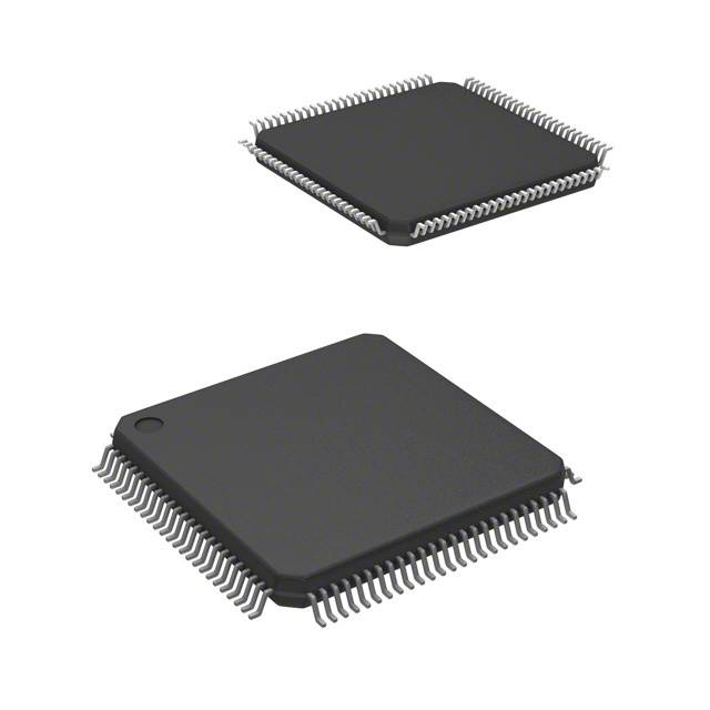


 工商网监
湘ICP备2023018690号
工商网监
湘ICP备2023018690号
