SAMA5D2 Series
Ultra-Low-Power Arm® Cortex®-A5 Core-Based MPU,
500 MHz, Graphics Interface, Ethernet 10/100, CAN, USB,
PCI 5.0 Pre-Certified
Introduction
The SAMA5D2 series is a high-performance, ultra-low-power Arm Cortex-A5 CPU-based embedded microprocessor
(MPU) running up to 500 MHz, with support for multiple memories such as DDR2, DDR3L, LPDDR2, LPDDR3, and
QSPI and e.MMC Flash. The devices integrate powerful peripherals for connectivity and user interface applications,
®
and offer advanced security functions (Arm TrustZone , tamper detection, secure data storage, etc.), as well as
high-performance crypto accelerators AES, SHA and TRNG.
Selected members of the SAMA5D2 series are qualified for extended industrial temperature range operation (-40°C
to 105°C external temperature).
®
The SAMA5D2 series is delivered with a free Linux distribution and bare metal C examples.
Features
•
•
•
Arm Cortex-A5 Core
– Armv7-A architecture
– Arm TrustZone
™
– NEON Media Processing Engine
– Up to 500 MHz
– ETM/ETB 8 Kbytes
Memory Architecture
– Memory Management Unit (MMU)
– 32-Kbyte L1 data cache, 32-Kbyte L1 instruction cache
– 128-Kbyte L2 cache configurable to be used as an internal SRAM
– One 128-Kbyte scrambled internal SRAM
– One 160-Kbyte internal ROM
• 64-Kbyte scrambled and maskable ROM embedding bootloader/Secure bootloader
• 96-Kbyte unscrambled, unmaskable ROM for NAND Flash BCH ECC table
– High-bandwidth scramblable 16-bit or 32-bit Double Data Rate (DDR) multiport dynamic RAM controller
supporting up to 512 Mbytes 8-bank DDR2/DDR3 (DLL off only) / DDR3L (DLL off only) / LPDDR1/
LPDDR2/LPDDR3, including “on-the-fly” encryption/decryption path
– 8-bit SLC/MLC NAND controller, with up to 32-bit Error Correcting Code (PMECC)
System Running up to 166 MHz in Typical Conditions
– Reset Controller (RSTC), Shutdown Controller (SHDWC), Periodic Interval Timer (PIT), independent
Watchdog Timer (WDT) and secure Real-Time Clock (RTC) with clock calibration
– One 600 to 1200 MHz PLL for the system and one 480 MHz PLL optimized for high-speed USB
– Digital fractional PLL for audio (11.2896 MHz and 12.288 MHz)
– Internal low-power 12 MHz RC and 32 kHz typical RC
– Selectable 32.768 Hz low-power oscillator and 8 to 24 MHz oscillator
– 51 DMA channels including two 16-channel 64-bit Central DMA Controllers
© 2021 Microchip Technology Inc.
Complete Datasheet
DS60001476G-page 1
�SAMA5D2 Series
•
•
– 64-bit Advanced Interrupt Controller (AIC)
– 64-bit Secure Advanced Interrupt Controller (SAIC)
– Three programmable external clock signals
Low-Power Modes
– Ultra-low-power mode with fast wake-up capability
– Low-power Backup mode with 5-Kbyte SRAM and SleepWalking™ features
• Wake up from up to nine wake-up pins, UART reception, analog comparison
• Fast wake-up capability
• Extended Backup mode with DDR in Self-Refresh mode
Peripherals
– LCD TFT controller (LCDC) up to 1024x768 or 1280x768 (still image). Four overlays, rotation, postprocessing and alpha blending, 24-bit parallel RGB interface
– ITU-R BT. 601/656/1120 Image Sensor Controller (ISC) supporting up to 5 Mpixel sensors with a parallel
12-bit interface for Raw Bayer, YCbCr, Monochrome and JPEG-compressed sensor interface
– Two Synchronous Serial Controllers (SSC), two Inter-IC Sound Controllers (I2SC), and one Stereo Class D
amplifier (CLASSD)
– One Peripheral Touch Controller (PTC) with up to 8 X-lines and 8 Y-lines (64-channel capacitive touch)
– One Pulse Density Modulation Interface Controller (PDMIC)
– One USB device high-speed port (UDPHS) and one USB host high-speed port or two USB host high-speed
ports (UHPHS)
– One USB host high-speed port with a High-Speed Inter-Chip (HSIC) interface
– One 10/100 Ethernet MAC (GMAC)
• Energy efficiency support (IEEE® 802.3az standard)
• Ethernet AVB support with IEEE802.1AS timestamping
• IEEE802.1Qav credit-based traffic-shaping hardware support
• IEEE1588 Precision Time Protocol (PTP)
– Two high-speed memory card hosts:
• SDMMC0: SD 3.0, eMMC 4.51, 8 bits
• SDMMC1: SD 2.0, eMMC 4.41, 4 bits only
– Two master/slave Serial Peripheral Interfaces (SPI)
– Two Quad Serial Peripheral Interfaces (QSPI)
– Five FLEXCOMs (USART, SPI and TWI)
– Five UARTs
– Two master CAN-FD (MCAN) controllers with SRAM-based mailboxes, and time- and event-triggered
transmission
WARNING
•
MCAN implements the non-ISO CAN FD frame format and therefore does not pass the CAN FD
Conformance Test according to ISO 16845-1:2016.
– One Rx only UART in backup area (RXLP)
– One Analog Comparator Controller (ACC) in backup area
– Two 2-wire interfaces (TWIHS) up to 400 Kbits/s supporting the I2C protocol and SMBUS
– One full-featured 4-channel 16-bit Pulse Width Modulation (PWM) controller
– Two 3-channel 32-bit Timer/Counters (TC), supporting basic PWM modes
– One 12-channel, 12-bit, Analog-to-Digital Converter (ADC) with resistive touchscreen capability
Safety
– Zero-power Power-on Reset (POR) cells
– Main crystal clock failure detector
– Write-protected registers
– Integrity Check Monitor (ICM) based on SHA256
© 2021 Microchip Technology Inc.
Complete Datasheet
DS60001476G-page 2
�SAMA5D2 Series
•
•
•
•
– Memory Management Unit (MMU)
– Independent watchdog
Security
– 5 Kbytes of internal scrambled SRAM:
• 1 Kbyte nonerasable on tamper detection
• 4 Kbytes erasable on tamper detection
– 256 bits of scrambled and erasable registers
– Up to eight tamper pins for static or dynamic intrusion detections(1)
– Environmental monitors on specific versions: temperature, voltage, frequency and active die shield(2)
– Secure Bootloader(3)
– On-the-fly AES encryption/decryption on DDR and QSPI memories (AESB)
– RTC including timestamping on security intrusions
– Programmable fuse box with 544 fuse bits (including JTAG protection and BMS)
Notes:
1. For information specific to dynamic tamper protection (PIOBU), refer to the document SAMA5D2
External Tamper Protections (document no. 44095).
2. For environmental monitors, refer to the document SAMA5D23 and SAMA5D28 Environmental
Monitors (document no. 44036), available under Non-Disclosure Agreement (NDA). Contact a
Microchip Sales Representative for details.
3. For secure boot strategies, refer to the document SAMA5D2 Series Secure Boot Strategy (document
no. DS00002435), available under Non-Disclosure Agreement (NDA). Contact a Microchip Sales
Representative for details.
Hardware Cryptography
– SHA (SHA1, SHA224, SHA256, SHA384, SHA512): compliant with FIPS PUB 180-2
– AES: 256-, 192-, 128-bit key algorithms, compliant with FIPS PUB 197
– TDES: two-key or three-key algorithms, compliant with FIPS PUB 46-3
– True Random Number Generator (TRNG) compliant with NIST Special Publication 800-22 Test Suite and
FIPS PUBs 140-2 and 140-3
Up to 128 I/Os
– Fully programmable through set/clear registers
– Multiplexing of up to eight peripheral functions per I/O line
– Each I/O line can be assigned to a peripheral or used as a general-purpose I/O
– The PIO controller features a synchronous output providing up to 32 bits of data output in one write
operation
Packages
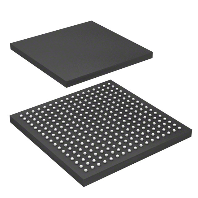
– 289-ball LFBGA, 14 x 14 mm body, 0.8 mm pitch
– 256-ball TFBGA, 8 x 8 mm body, 0.4 mm pitch
– 196-ball TFBGA, 11 x 11 mm body, 0.75 mm pitch
© 2021 Microchip Technology Inc.
Complete Datasheet
DS60001476G-page 3
�SAMA5D2 Series
Table of Contents
Introduction.....................................................................................................................................................1
Features......................................................................................................................................................... 1
1.
Description............................................................................................................................................ 17
2.
Configuration Summary........................................................................................................................ 18
3.
Block Diagram.......................................................................................................................................19
4.
Signal Description................................................................................................................................. 20
5.
Microchip Recommended Power Management Solutions.................................................................... 26
5.1.
5.2.
6.
Safety and Security Features................................................................................................................29
6.1.
6.2.
6.3.
6.4.
7.
Packages....................................................................................................................................33
Pinouts....................................................................................................................................... 33
Power Considerations........................................................................................................................... 66
8.1.
8.2.
8.3.
8.4.
9.
Design for Safety and IEC60730 Class B Certification.............................................................. 29
Design for Security..................................................................................................................... 29
Safety and IEC 60730 Features................................................................................................. 29
Security Features....................................................................................................................... 30
Package and Pinout.............................................................................................................................. 33
7.1.
7.2.
8.
MCP16502 PMIC....................................................................................................................... 26
MCP16501 PMIC....................................................................................................................... 27
Power Supplies ......................................................................................................................... 66
Power-up Considerations........................................................................................................... 66
Power-down Considerations...................................................................................................... 68
Power Supply Sequencing at Backup Mode Entry and Exit.......................................................68
Memories.............................................................................................................................................. 71
9.1.
9.2.
Embedded Memories................................................................................................................. 72
External Memory........................................................................................................................ 72
10. Event System........................................................................................................................................ 76
10.1. Real-time Event List................................................................................................................... 76
10.2. Real-time Event Mapping........................................................................................................... 76
11. System Controller..................................................................................................................................78
11.1. Power-On Reset.........................................................................................................................80
12. Peripherals............................................................................................................................................ 81
12.1.
12.2.
12.3.
12.4.
Peripheral Mapping.................................................................................................................... 81
Peripheral Identifiers.................................................................................................................. 81
Peripheral Signal Multiplexing on I/O Lines................................................................................81
Peripheral Clock Types.............................................................................................................. 81
13. Chip Identifier (CHIPID)........................................................................................................................ 83
© 2021 Microchip Technology Inc.
Complete Datasheet
DS60001476G-page 4
�SAMA5D2 Series
13.1. Description................................................................................................................................. 83
13.2. Embedded Characteristics......................................................................................................... 83
13.3. Register Summary......................................................................................................................85
14. Cortex-A5 Processor (ARM)................................................................................................................. 90
14.1.
14.2.
14.3.
14.4.
14.5.
14.6.
Reference Documents................................................................................................................90
Description................................................................................................................................. 90
Embedded Characteristics......................................................................................................... 91
Block Diagram............................................................................................................................ 91
Programmer Model.....................................................................................................................91
Memory Management Unit (MMU) ............................................................................................ 98
15. L2 Cache Controller (L2CC)................................................................................................................103
15.1.
15.2.
15.3.
15.4.
15.5.
Description............................................................................................................................... 103
Embedded Characteristics....................................................................................................... 103
Product Dependencies............................................................................................................. 103
Functional Description..............................................................................................................103
Register Summary....................................................................................................................105
16. Debug and Test Features....................................................................................................................140
16.1.
16.2.
16.3.
16.4.
16.5.
16.6.
16.7.
16.8.
Description............................................................................................................................... 140
Embedded Characteristics....................................................................................................... 140
Debug and Test Block Diagrams.............................................................................................. 141
Application Examples............................................................................................................... 142
Debug and Test Pin Description............................................................................................... 144
Functional Description..............................................................................................................144
Boundary JTAG ID Register..................................................................................................... 146
Cortex-A5 DP Identification Code Register IDCODE............................................................... 146
17. Standard Boot Strategies.................................................................................................................... 149
17.1.
17.2.
17.3.
17.4.
17.5.
17.6.
17.7.
Description............................................................................................................................... 149
Chip Access Using JTAG Connection...................................................................................... 149
Flow Diagram........................................................................................................................... 149
Chip Setup................................................................................................................................149
Boot Configuration....................................................................................................................150
SAM-BA Monitor.......................................................................................................................176
Fuse Box Controller..................................................................................................................180
18. AXI Matrix (AXIMX)............................................................................................................................. 182
18.1.
18.2.
18.3.
18.4.
Description............................................................................................................................... 182
Embedded Characteristics....................................................................................................... 182
Operation..................................................................................................................................182
Register Summary....................................................................................................................183
19. Matrix (H64MX/H32MX)...................................................................................................................... 185
19.1.
19.2.
19.3.
19.4.
Description............................................................................................................................... 185
Embedded Characteristics....................................................................................................... 185
64-bit Matrix (H64MX).............................................................................................................. 185
32-bit Matrix (H32MX).............................................................................................................. 188
© 2021 Microchip Technology Inc.
Complete Datasheet
DS60001476G-page 5
�SAMA5D2 Series
19.5. Memory Mapping......................................................................................................................189
19.6. Special Bus Granting Mechanism............................................................................................ 190
19.7. No Default Master.................................................................................................................... 190
19.8. Last Access Master.................................................................................................................. 190
19.9. Fixed Default Master................................................................................................................ 190
19.10. Arbitration.................................................................................................................................191
19.11. Register Write Protection......................................................................................................... 193
19.12. TrustZone Technology..............................................................................................................193
19.13. Register Summary................................................................................................................... 209
20. Special Function Registers (SFR).......................................................................................................231
20.1. Description............................................................................................................................... 231
20.2. Embedded Characteristics....................................................................................................... 231
20.3. Register Summary....................................................................................................................232
21. Special Function Registers Backup (SFRBU).....................................................................................250
21.1. Description............................................................................................................................... 250
21.2. Embedded Characteristics....................................................................................................... 250
21.3. Register Summary....................................................................................................................251
22. Advanced Interrupt Controller (AIC)....................................................................................................257
22.1.
22.2.
22.3.
22.4.
22.5.
22.6.
22.7.
22.8.
22.9.
Description............................................................................................................................... 257
Embedded Characteristics....................................................................................................... 257
Block Diagram.......................................................................................................................... 258
Application Block Diagram....................................................................................................... 258
AIC Detailed Block Diagram.....................................................................................................259
I/O Line Description..................................................................................................................259
Product Dependencies............................................................................................................. 259
Functional Description..............................................................................................................260
Register Summary....................................................................................................................268
23. Watchdog Timer (WDT).......................................................................................................................291
23.1.
23.2.
23.3.
23.4.
23.5.
Description............................................................................................................................... 291
Embedded Characteristics....................................................................................................... 291
Block Diagram.......................................................................................................................... 291
Functional Description..............................................................................................................291
Register Summary....................................................................................................................294
24. Reset Controller (RSTC)..................................................................................................................... 299
24.1.
24.2.
24.3.
24.4.
24.5.
Description............................................................................................................................... 299
Embedded Characteristics....................................................................................................... 299
Block Diagram.......................................................................................................................... 299
Functional Description..............................................................................................................299
Register Summary....................................................................................................................305
25. Shutdown Controller (SHDWC)...........................................................................................................309
25.1. Description............................................................................................................................... 309
25.2. Embedded Characteristics....................................................................................................... 309
25.3. Block Diagram.......................................................................................................................... 309
© 2021 Microchip Technology Inc.
Complete Datasheet
DS60001476G-page 6
�SAMA5D2 Series
25.4.
25.5.
25.6.
25.7.
I/O Lines Description................................................................................................................ 310
Product Dependencies............................................................................................................. 310
Functional Description..............................................................................................................310
Register Summary....................................................................................................................312
26. Periodic Interval Timer (PIT)............................................................................................................... 318
26.1.
26.2.
26.3.
26.4.
26.5.
Description............................................................................................................................... 318
Embedded Characteristics....................................................................................................... 318
Block Diagram.......................................................................................................................... 318
Functional Description..............................................................................................................318
Register Summary....................................................................................................................320
27. Real-time Clock (RTC)........................................................................................................................ 325
27.1.
27.2.
27.3.
27.4.
27.5.
27.6.
Description............................................................................................................................... 325
Embedded Characteristics....................................................................................................... 325
Block Diagram.......................................................................................................................... 325
Product Dependencies............................................................................................................. 326
Functional Description..............................................................................................................326
Register Summary....................................................................................................................336
28. System Controller Write Protection (SYSCWP).................................................................................. 365
28.1. Functional Description..............................................................................................................365
28.2. Register Summary....................................................................................................................366
29. Slow Clock Controller (SCKC)............................................................................................................ 368
29.1.
29.2.
29.3.
29.4.
29.5.
Description............................................................................................................................... 368
Embedded Characteristics....................................................................................................... 368
Block Diagram.......................................................................................................................... 368
Functional Description..............................................................................................................368
Register Summary....................................................................................................................370
30. Peripheral Touch Controller (PTC)...................................................................................................... 372
30.1.
30.2.
30.3.
30.4.
30.5.
30.6.
30.7.
Description............................................................................................................................... 372
Embedded Characteristics....................................................................................................... 372
Block Diagram.......................................................................................................................... 373
Signal Description.................................................................................................................... 373
Product Dependencies............................................................................................................. 374
Functional Description..............................................................................................................375
Register Summary....................................................................................................................380
31. Low Power Asynchronous Receiver (RXLP).......................................................................................384
31.1.
31.2.
31.3.
31.4.
31.5.
31.6.
Description............................................................................................................................... 384
Embedded Characteristics....................................................................................................... 384
Block Diagram.......................................................................................................................... 384
Product Dependencies............................................................................................................. 384
Functional Description..............................................................................................................385
Register Summary....................................................................................................................387
32. Clock Generator.................................................................................................................................. 394
© 2021 Microchip Technology Inc.
Complete Datasheet
DS60001476G-page 7
�SAMA5D2 Series
32.1.
32.2.
32.3.
32.4.
32.5.
32.6.
32.7.
32.8.
Description............................................................................................................................... 394
Embedded Characteristics....................................................................................................... 394
Block Diagram.......................................................................................................................... 395
Slow Clock................................................................................................................................395
Main Clock................................................................................................................................396
Divider and PLLA Block............................................................................................................399
UTMI PLL Clock....................................................................................................................... 400
Audio PLL.................................................................................................................................400
33. Power Management Controller (PMC)................................................................................................ 402
33.1. Description............................................................................................................................... 402
33.2. Embedded Characteristics....................................................................................................... 402
33.3. Block Diagram.......................................................................................................................... 403
33.4. Master Clock Controller............................................................................................................404
33.5. Processor Clock Controller.......................................................................................................404
33.6. Matrix Clock Controller............................................................................................................. 404
33.7. Programmable Clock Controller............................................................................................... 405
33.8. Core and Bus Independent Clocks for Peripherals.................................................................. 405
33.9. Peripheral and Generic Clock Controller..................................................................................406
33.10. LCDC Clock Controller.............................................................................................................406
33.11. ISC Clock Controller.................................................................................................................407
33.12. USB Device and Host Clocks...................................................................................................407
33.13. DDR2/LPDDR/LPDDR2 Clock Controller................................................................................ 407
33.14. Fast Start-up from Ultra-Low-Power (ULP) Mode 0................................................................. 407
33.15. Fast Start-up from Ultra-Low-Power (ULP) Mode 1................................................................. 408
33.16. Asynchronous Partial Wake-up (SleepWalking).......................................................................410
33.17. Main Crystal Oscillator Failure Detection................................................................................. 412
33.18. 32.768 kHz Crystal Oscillator Frequency Monitor....................................................................413
33.19. Programming Sequence.......................................................................................................... 413
33.20. Clock Switching Details............................................................................................................415
33.21. Register Write Protection......................................................................................................... 418
33.22. Register Summary................................................................................................................... 419
34. Parallel Input/Output Controller (PIO)................................................................................................. 472
34.1.
34.2.
34.3.
34.4.
34.5.
34.6.
34.7.
Description............................................................................................................................... 472
Embedded Characteristics....................................................................................................... 472
Block Diagram.......................................................................................................................... 473
Product Dependencies............................................................................................................. 474
Functional Description..............................................................................................................474
I/O Lines Programming Example............................................................................................. 484
Register Summary....................................................................................................................487
35. External Memories.............................................................................................................................. 534
35.1. Multiport DDR-SDRAM Controller (MPDDRC).........................................................................534
35.2. External Bus Interface (EBI).....................................................................................................542
36. AHB Multiport DDR-SDRAM Controller (MPDDRC)........................................................................... 544
36.1. Description............................................................................................................................... 544
36.2. Embedded Characteristics....................................................................................................... 544
© 2021 Microchip Technology Inc.
Complete Datasheet
DS60001476G-page 8
�SAMA5D2 Series
36.3.
36.4.
36.5.
36.6.
36.7.
Block Diagram.......................................................................................................................... 545
Product Dependencies, Initialization Sequence....................................................................... 546
Functional Description..............................................................................................................553
Software Interface/SDRAM Organization, Address Mapping...................................................566
Register Summary....................................................................................................................573
37. Static Memory Controller (SMC)......................................................................................................... 621
37.1. Description............................................................................................................................... 621
37.2. Embedded Characteristics....................................................................................................... 621
37.3. Block Diagram.......................................................................................................................... 622
37.4. I/O Lines Description................................................................................................................ 622
37.5. Multiplexed Signals.................................................................................................................. 623
37.6. Application Example.................................................................................................................623
37.7. Product Dependencies............................................................................................................. 623
37.8. External Memory Mapping....................................................................................................... 624
37.9. Connection to External Devices............................................................................................... 624
37.10. Standard Read and Write Protocols.........................................................................................626
37.11. Scrambling/Unscrambling Function..........................................................................................632
37.12. Automatic Wait States..............................................................................................................632
37.13. Data Float Wait States............................................................................................................. 636
37.14. External Wait............................................................................................................................640
37.15. Slow Clock Mode..................................................................................................................... 644
37.16. Register Write Protection......................................................................................................... 646
37.17. NFC Operations....................................................................................................................... 646
37.18. PMECC Controller Functional Description............................................................................... 656
37.19. Software Implementation......................................................................................................... 662
37.20. Register Summary................................................................................................................... 667
38. DMA Controller (XDMAC)................................................................................................................... 719
38.1.
38.2.
38.3.
38.4.
38.5.
38.6.
38.7.
38.8.
38.9.
Description............................................................................................................................... 719
Embedded Characteristics....................................................................................................... 719
Block Diagram.......................................................................................................................... 720
DMA Controller Peripheral Connections.................................................................................. 720
Functional Description..............................................................................................................724
Linked List Descriptor Operation.............................................................................................. 730
XDMAC Maintenance Software Operations............................................................................. 732
XDMAC Software Requirements..............................................................................................732
Register Summary....................................................................................................................734
39. LCD Controller (LCDC)....................................................................................................................... 789
39.1.
39.2.
39.3.
39.4.
39.5.
39.6.
39.7.
Description............................................................................................................................... 789
Embedded Characteristics....................................................................................................... 789
Block Diagram.......................................................................................................................... 790
I/O Lines Description................................................................................................................ 790
Product Dependencies............................................................................................................. 791
Functional Description..............................................................................................................791
Register Summary....................................................................................................................820
40. Ethernet MAC (GMAC)..................................................................................................................... 1005
© 2021 Microchip Technology Inc.
Complete Datasheet
DS60001476G-page 9
�SAMA5D2 Series
40.1.
40.2.
40.3.
40.4.
40.5.
40.6.
40.7.
40.8.
Description............................................................................................................................. 1005
Embedded Characteristics..................................................................................................... 1005
Block Diagram........................................................................................................................ 1006
Signal Interfaces.....................................................................................................................1006
Product Dependencies........................................................................................................... 1007
Functional Description............................................................................................................1007
Programming Interface...........................................................................................................1032
Register Summary..................................................................................................................1037
41. USB High Speed Device Port (UDPHS)............................................................................................1184
41.1.
41.2.
41.3.
41.4.
41.5.
41.6.
41.7.
Description..............................................................................................................................1184
Embedded Characteristics..................................................................................................... 1184
Block Diagram........................................................................................................................ 1185
Typical Connection................................................................................................................. 1185
Product Dependencies........................................................................................................... 1186
Functional Description............................................................................................................ 1186
Register Summary..................................................................................................................1208
42. USB Host High Speed Port (UHPHS)............................................................................................... 1279
42.1.
42.2.
42.3.
42.4.
42.5.
42.6.
42.7.
Description............................................................................................................................. 1279
Embedded Characteristics..................................................................................................... 1279
Block Diagram........................................................................................................................ 1280
Typical Connection................................................................................................................. 1281
Product Dependencies........................................................................................................... 1281
Functional Description............................................................................................................1282
Register Summary..................................................................................................................1284
43. Audio Class D Amplifier (CLASSD)...................................................................................................1310
43.1.
43.2.
43.3.
43.4.
43.5.
43.6.
43.7.
Description............................................................................................................................. 1310
Embedded Characteristics..................................................................................................... 1310
Block Diagram........................................................................................................................ 1311
Pin Name List......................................................................................................................... 1311
Product Dependencies........................................................................................................... 1312
Functional Description............................................................................................................1312
Register Summary..................................................................................................................1325
44. Inter-IC Sound Controller (I2SC).......................................................................................................1338
44.1.
44.2.
44.3.
44.4.
44.5.
44.6.
44.7.
44.8.
Description............................................................................................................................. 1338
Embedded Characteristics..................................................................................................... 1338
Block Diagram........................................................................................................................ 1339
I/O Lines Description.............................................................................................................. 1339
Product Dependencies........................................................................................................... 1339
Functional Description............................................................................................................1340
I2SC Application Examples.................................................................................................... 1344
Register Summary..................................................................................................................1348
45. Synchronous Serial Controller (SSC)................................................................................................1363
45.1. Description............................................................................................................................. 1363
45.2. Embedded Characteristics..................................................................................................... 1363
© 2021 Microchip Technology Inc.
Complete Datasheet
DS60001476G-page 10
�SAMA5D2 Series
45.3.
45.4.
45.5.
45.6.
45.7.
45.8.
45.9.
Block Diagram........................................................................................................................ 1364
Application Block Diagram..................................................................................................... 1364
SSC Application Examples.....................................................................................................1364
Pin Name List......................................................................................................................... 1366
Product Dependencies........................................................................................................... 1366
Functional Description............................................................................................................1367
Register Summary..................................................................................................................1377
46. Two-wire Interface (TWIHS)..............................................................................................................1405
46.1.
46.2.
46.3.
46.4.
46.5.
46.6.
46.7.
Description............................................................................................................................. 1405
Embedded Characteristics..................................................................................................... 1405
List of Abbreviations............................................................................................................... 1406
Block Diagram........................................................................................................................ 1406
Product Dependencies........................................................................................................... 1407
Functional Description............................................................................................................1407
Register Summary..................................................................................................................1453
47. Flexible Serial Communication Controller (FLEXCOM).................................................................... 1500
47.1. Description............................................................................................................................. 1500
47.2. Embedded Characteristics..................................................................................................... 1501
47.3. Block Diagram........................................................................................................................ 1503
47.4. I/O Lines Description.............................................................................................................. 1503
47.5. Product Dependencies........................................................................................................... 1504
47.6. Register Accesses..................................................................................................................1504
47.7. USART Functional Description...............................................................................................1504
47.8. SPI Functional Description..................................................................................................... 1548
47.9. TWI Functional Description.................................................................................................... 1568
47.10. Register Summary................................................................................................................. 1612
48. Universal Asynchronous Receiver Transmitter (UART).................................................................... 1751
48.1.
48.2.
48.3.
48.4.
48.5.
48.6.
Description............................................................................................................................. 1751
Embedded Characteristics..................................................................................................... 1751
Block Diagram........................................................................................................................ 1751
Product Dependencies........................................................................................................... 1752
Functional Description............................................................................................................1752
Register Summary..................................................................................................................1762
49. Serial Peripheral Interface (SPI)....................................................................................................... 1777
49.1.
49.2.
49.3.
49.4.
49.5.
49.6.
49.7.
49.8.
Description............................................................................................................................. 1777
Embedded Characteristics..................................................................................................... 1777
Block Diagram........................................................................................................................ 1778
Application Block Diagram..................................................................................................... 1778
Signal Description.................................................................................................................. 1779
Product Dependencies........................................................................................................... 1779
Functional Description............................................................................................................1779
Register Summary..................................................................................................................1799
50. Quad Serial Peripheral Interface (QSPI)...........................................................................................1827
50.1. Description............................................................................................................................. 1827
© 2021 Microchip Technology Inc.
Complete Datasheet
DS60001476G-page 11
�SAMA5D2 Series
50.2.
50.3.
50.4.
50.5.
50.6.
50.7.
Embedded Characteristics..................................................................................................... 1827
Block Diagram........................................................................................................................ 1828
Signal Description.................................................................................................................. 1828
Product Dependencies........................................................................................................... 1828
Functional Description............................................................................................................1829
Register Summary..................................................................................................................1845
51. Secure Digital MultiMedia Card Controller (SDMMC)....................................................................... 1866
51.1. Description............................................................................................................................. 1866
51.2. Embedded Characteristics..................................................................................................... 1866
51.3. Reference Documents............................................................................................................1866
51.4. Block Diagram........................................................................................................................ 1867
51.5. Application Block Diagram..................................................................................................... 1868
51.6. Pin Name List......................................................................................................................... 1868
51.7. Product Dependencies........................................................................................................... 1868
51.8. SD/SDIO Operating Mode......................................................................................................1869
51.9. e.MMC Operating Mode......................................................................................................... 1869
51.10. SDR104 / HS200 Tuning........................................................................................................1871
51.11. I/O Calibration........................................................................................................................ 1873
51.12. Register Summary................................................................................................................. 1874
52. Image Sensor Controller (ISC)..........................................................................................................1967
52.1.
52.2.
52.3.
52.4.
52.5.
52.6.
52.7.
Description............................................................................................................................. 1967
Embedded Characteristics..................................................................................................... 1967
Block Diagram and Use Cases.............................................................................................. 1968
I/O Lines Description.............................................................................................................. 1969
Product Dependencies........................................................................................................... 1971
Functional Description............................................................................................................1971
Register Summary..................................................................................................................1991
53. Controller Area Network (MCAN)......................................................................................................2063
53.1.
53.2.
53.3.
53.4.
53.5.
53.6.
Description............................................................................................................................. 2063
Embedded Characteristics..................................................................................................... 2063
Block Diagram........................................................................................................................ 2064
Product Dependencies........................................................................................................... 2064
Functional Description............................................................................................................2065
Register Summary..................................................................................................................2090
54. Timer Counter (TC)........................................................................................................................... 2149
54.1.
54.2.
54.3.
54.4.
54.5.
54.6.
54.7.
Description............................................................................................................................. 2149
Embedded Characteristics..................................................................................................... 2149
Block Diagram........................................................................................................................ 2150
Pin List....................................................................................................................................2151
Product Dependencies........................................................................................................... 2151
Functional Description............................................................................................................2151
Register Summary..................................................................................................................2174
55. Pulse Density Modulation Interface Controller (PDMIC)................................................................... 2206
55.1. Description............................................................................................................................. 2206
© 2021 Microchip Technology Inc.
Complete Datasheet
DS60001476G-page 12
�SAMA5D2 Series
55.2.
55.3.
55.4.
55.5.
55.6.
55.7.
Embedded Characteristics..................................................................................................... 2206
Block Diagram........................................................................................................................ 2206
Signal Description.................................................................................................................. 2206
Product Dependencies........................................................................................................... 2207
Functional Description............................................................................................................2207
Register Summary..................................................................................................................2212
56. Pulse Width Modulation Controller (PWM)........................................................................................2224
56.1.
56.2.
56.3.
56.4.
56.5.
56.6.
56.7.
Description............................................................................................................................. 2224
Embedded Characteristics..................................................................................................... 2224
Block Diagram........................................................................................................................ 2226
I/O Lines Description.............................................................................................................. 2226
Product Dependencies........................................................................................................... 2227
Functional Description............................................................................................................2228
Register Summary..................................................................................................................2266
57. Secure Fuse Controller (SFC)...........................................................................................................2328
57.1.
57.2.
57.3.
57.4.
57.5.
Description............................................................................................................................. 2328
Embedded Characteristics..................................................................................................... 2328
Block Diagram........................................................................................................................ 2328
Functional Description............................................................................................................2329
Register Summary..................................................................................................................2331
58. Integrity Check Monitor (ICM)........................................................................................................... 2339
58.1.
58.2.
58.3.
58.4.
58.5.
58.6.
Description............................................................................................................................. 2339
Embedded Characteristics..................................................................................................... 2340
Block Diagram........................................................................................................................ 2340
Product Dependencies........................................................................................................... 2341
Functional Description............................................................................................................2341
Register Summary..................................................................................................................2354
59. Advanced Encryption Standard Bridge (AESB)................................................................................ 2373
59.1.
59.2.
59.3.
59.4.
59.5.
Description............................................................................................................................. 2373
Embedded Characteristics..................................................................................................... 2373
Product Dependencies........................................................................................................... 2373
Functional Description............................................................................................................2373
Register Summary..................................................................................................................2377
60. Advanced Encryption Standard (AES).............................................................................................. 2390
60.1.
60.2.
60.3.
60.4.
60.5.
Description............................................................................................................................. 2390
Embedded Characteristics..................................................................................................... 2390
Product Dependencies........................................................................................................... 2390
Functional Description............................................................................................................2391
Register Summary..................................................................................................................2410
61. Secure Hash Algorithm (SHA).......................................................................................................... 2437
61.1. Description............................................................................................................................. 2437
61.2. Embedded Characteristics..................................................................................................... 2437
61.3. Product Dependencies........................................................................................................... 2437
© 2021 Microchip Technology Inc.
Complete Datasheet
DS60001476G-page 13
�SAMA5D2 Series
61.4. Functional Description............................................................................................................2437
61.5. Register Summary..................................................................................................................2445
62. Triple Data Encryption Standard (TDES).......................................................................................... 2459
62.1.
62.2.
62.3.
62.4.
62.5.
Description............................................................................................................................. 2459
Embedded Characteristics..................................................................................................... 2459
Product Dependencies........................................................................................................... 2459
Functional Description............................................................................................................2460
Register Summary..................................................................................................................2466
63. True Random Number Generator (TRNG)........................................................................................2482
63.1.
63.2.
63.3.
63.4.
63.5.
63.6.
Description............................................................................................................................. 2482
Embedded Characteristics..................................................................................................... 2482
Block Diagram........................................................................................................................ 2482
Product Dependencies........................................................................................................... 2482
Functional Description............................................................................................................2483
Register Summary..................................................................................................................2484
64. Analog Comparator Controller (ACC)............................................................................................... 2491
64.1.
64.2.
64.3.
64.4.
64.5.
64.6.
64.7.
Description............................................................................................................................. 2491
Embedded Characteristics..................................................................................................... 2491
Block Diagram........................................................................................................................ 2491
Signal Description.................................................................................................................. 2491
Product Dependencies........................................................................................................... 2491
Functional Description............................................................................................................2492
Register Summary..................................................................................................................2493
65. Security Module (SECUMOD)...........................................................................................................2498
65.1.
65.2.
65.3.
65.4.
65.5.
65.6.
Description............................................................................................................................. 2498
Embedded Characteristics..................................................................................................... 2498
Block Diagram........................................................................................................................ 2499
Product Dependencies........................................................................................................... 2500
Functional Description............................................................................................................2500
Register Summary..................................................................................................................2507
66. Analog-to-Digital Controller (ADC).................................................................................................... 2527
66.1.
66.2.
66.3.
66.4.
66.5.
66.6.
66.7.
Description............................................................................................................................. 2527
Embedded Characteristics..................................................................................................... 2527
Block Diagram........................................................................................................................ 2528
Signal Description.................................................................................................................. 2528
Product Dependencies........................................................................................................... 2529
Functional Description............................................................................................................2529
Register Summary..................................................................................................................2555
67. Electrical Characteristics...................................................................................................................2592
67.1.
67.2.
67.3.
67.4.
Absolute Maximum Ratings....................................................................................................2592
DC Characteristics................................................................................................................. 2592
Power Consumption............................................................................................................... 2595
Active Mode............................................................................................................................2596
© 2021 Microchip Technology Inc.
Complete Datasheet
DS60001476G-page 14
�SAMA5D2 Series
67.5. Low-power Modes.................................................................................................................. 2598
67.6. Clock Characteristics..............................................................................................................2603
67.7. Oscillator Characteristics........................................................................................................2604
67.8. PLL Characteristics................................................................................................................ 2607
67.9. USB HS Characteristics......................................................................................................... 2608
67.10. PTC Characteristics............................................................................................................... 2608
67.11. ADC Characteristics............................................................................................................... 2609
67.12. Analog Comparator Characteristics....................................................................................... 2614
67.13. POR Characteristics...............................................................................................................2615
67.14. SMC Timings..........................................................................................................................2616
67.15. FLEXCOM Timings................................................................................................................ 2620
67.16. USART in Asynchronous Modes............................................................................................2629
67.17. SPI Timings............................................................................................................................2629
67.18. TWI Timings........................................................................................................................... 2635
67.19. QSPI Timings......................................................................................................................... 2637
67.20. MPDDRC Timings..................................................................................................................2641
67.21. SSC Timings.......................................................................................................................... 2643
67.22. PDMIC Timings...................................................................................................................... 2649
67.23. I2SC Timings..........................................................................................................................2650
67.24. ISC Timings............................................................................................................................2652
67.25. SDMMC Timings.................................................................................................................... 2653
67.26. GMAC Timings.......................................................................................................................2654
68. Mechanical Characteristics............................................................................................................... 2657
68.1. 289-Ball Low Profile Fine Pitch Ball Grid Array (AMB) - 14x14x1.4 mm Body [LFBGA] Atmel
Legacy Global Package Code CCZ....................................................................................... 2657
68.2. 256-Ball Thin Fine Pitch Ball Grid Array (AYB) - 8x8x1.05 mm Body [TFBGA]..................... 2661
68.3. 196-Ball Thin Fine Pitch Ball Grid Array (BAB) - 11x11 mm Body [TFBGA]...........................2665
69. Schematic Checklist..........................................................................................................................2669
69.1. Power Supply......................................................................................................................... 2669
69.2. Power-On Reset.....................................................................................................................2673
69.3. Clock, Oscillator and PLL....................................................................................................... 2674
69.4. ICE and JTAG........................................................................................................................ 2675
69.5. Reset and Test....................................................................................................................... 2677
69.6. Shutdown/Wake-up Logic.......................................................................................................2677
69.7. Parallel Input/Output (PIO)..................................................................................................... 2678
69.8. Analog-to-Digital Converter (ADC)......................................................................................... 2678
69.9. External Bus Interface (EBI)...................................................................................................2678
69.10. USB High-Speed Host Port (UHPHS) / USB High-Speed Device Port (UDPHS)..................2680
69.11. Boot Program Hardware Constraints..................................................................................... 2681
69.12. Layout and Design Constraints.............................................................................................. 2681
70. Marking............................................................................................................................................. 2685
71. Ordering Information......................................................................................................................... 2686
72. Revision History................................................................................................................................ 2687
72.1. Revision DS60001476G - 03/2021.........................................................................................2687
© 2021 Microchip Technology Inc.
Complete Datasheet
DS60001476G-page 15
�SAMA5D2 Series
72.2. Revision DS60001476F - 09/2020......................................................................................... 2687
72.3. Revision DS60001476E - 09/2020......................................................................................... 2687
72.4. Revision DS60001476D - 02/2020.........................................................................................2688
72.5. Revision DS60001476C......................................................................................................... 2693
72.6. Revision DS60001476B......................................................................................................... 2697
72.7. Revision DS60001476A......................................................................................................... 2698
72.8. Revision 11267E.................................................................................................................... 2706
72.9. Revision 11267D.................................................................................................................... 2706
72.10. Revision 11267C.................................................................................................................... 2715
72.11. Revision 11267B.................................................................................................................... 2719
72.12. Revision 11267A.................................................................................................................... 2722
The Microchip Website.............................................................................................................................2723
Product Change Notification Service........................................................................................................2723
Customer Support.................................................................................................................................... 2723
Product Identification System...................................................................................................................2724
Microchip Devices Code Protection Feature............................................................................................ 2724
Legal Notice............................................................................................................................................. 2725
Trademarks.............................................................................................................................................. 2725
Quality Management System................................................................................................................... 2726
Worldwide Sales and Service...................................................................................................................2727
© 2021 Microchip Technology Inc.
Complete Datasheet
DS60001476G-page 16
�SAMA5D2 Series
Description
1.
Description
The SAMA5D2 Series is a high-performance, power-efficient embedded MPU based on the Arm Cortex-A5
processor. It integrates the Arm NEON SIMD engine for accelerated multimedia and signal processing, a configurable
128-Kbyte L2 cache and a floating point unit (FPU) for high-precision computing. The device features an advanced
user interface and connectivity peripherals. Advanced security is provided by powerful cryptographic accelerators,
by the Arm TrustZone technology securing access to memories and sensitive peripherals, and by several hardware
features that safeguard memory content, authenticate software, detect physical attacks and prevent information
leakage during code execution.
The SAMA5D2 features an internal multilayer bus architecture associated with 2 x 16 DMA channels and dedicated
DMAs for the communication and interface peripherals required to ensure uninterrupted data transfers with minimal
processor overhead. The device supports DDR2, DDR3, DDR3L, LPDDR1, LPDDR2, LPDDR3, QSPI and e.MMC
Flash, and SLC/MLC parallel NAND Flash memory up to 32-bit ECC.
The comprehensive peripheral set includes an LCD TFT controller with overlays for hardware-accelerated image
composition, an image sensor controller, audio support through I2S, SSC, a stereo Class D amplifier and a digital
microphone. Connectivity peripherals include a 10/100 EMAC, USBs, CANs, FLEXCOMs, UARTs, SPIs and two
QSPIs, SDIO/SD/e.MMCs, and TWIs/I2C.
Protection of code and data is provided by automatic scrambling of memories and an Integrity Check Monitor (ICM)
to detect any modification of the memory contents. The SAMA5D2 also supports execution of encrypted code (QSPI
or one portion of the DDR) with an “on-the-fly” encryption-decryption process.
With its secure design architecture, cryptographic acceleration engines, and secure bootloader, the SAMA5D2 is the
ideal solution for point-of-sale (POS), IoT and industrial applications requiring device authentication, anti-cloning, data
protection and secure communication.
SAMA5D2 devices feature three software-selectable low-power modes: Idle, Ultra-Low-Power and Backup.
In Idle mode, the processor is stopped while all other functions can be kept running.
In Ultra-Low-Power mode 0, the processor is stopped while all other functions are clocked at 512 Hz and interrupts
or peripherals can be configured to wake up the system based on events, including partial asynchronous wake-up
(SleepWalking).
In Ultra-Low-Power mode 1, all clocks and functions are stopped but some peripherals can be configured to wake up
the system based on events, including partial asynchronous wake-up (SleepWalking).
In Backup mode, RTC and wake-up logic are active. The Backup mode can be extended to feature DDR in Selfrefresh mode.
SAMA5D2 devices also include an Event System that allows peripherals to receive, react to and send events in
Active and Idle modes without processor intervention.
© 2021 Microchip Technology Inc.
Complete Datasheet
DS60001476G-page 17
�SAMA5D2 Series
Configuration Summary
2.
Configuration Summary
Table 2-1. SAMA5D2 Configuration Summary
Feature
SAMA5D21
SAMA5D22
Package
PIOs
DDR Bus
SAMA5D23
SAMA5D24
SAMA5D26
TFBGA196
TFBGA256
LFBGA289
72
105
128
16-bit
Up to 16-bit
SRAM
128 Kbytes
QSPI
2
LCD
24-bit RGB
Camera Interface
(ISC)
1
EMAC
1
PTC
–
4 X-lines x 8 Y-lines
CAN
–
1
8 X-lines x
8 Y-lines
–
8 X-lines x 8 Y-lines
–
2
(2 Hosts
or
1 Host/1 Device)
3
(2 Hosts/
1 HSIC,
or
1 Host/
1 Device/
1 HSIC)
2
2
(2 Hosts
or
1 Host/
1 Device)
3
(2 Hosts/1 HSIC
or
1 Host/1 Device/1 HSIC)
UART/SPI/I2C
9/6/6
10 / 7 / 7
SDIO/SD/MMC
1
2
I2S/SSC/
Class D/PDM
2/2/1/1
ADC Inputs
5
12
Timers
5
6
PWM
4 (PWM) + 5 (TC)
4 (PWM) + 6 (TC)
Tamper Pins
AESB
6
–
Environmental
Monitors,
Die Shield
SAMA5D28
16/32-bit
SMC
USB
SAMA5D27
–
2
8
Yes
–
Yes
–
Yes
Yes
For information on device pin compatibility, see the section "Pinouts".
© 2021 Microchip Technology Inc.
Complete Datasheet
DS60001476G-page 18
�SAMA5D2 Series
Block Diagram
Block Diagram
Figure 3-1. SAMA5D2 Series Block Diagram
PIO
JTAG / SWD
Key
Digital
In-Circuit Emulator
L1 32-KB
ICache
Master
Slave
NEON
FPU
Cortex-A5 Processor
EBI
L1 32-KB
DCache
MMU
L2 Cache
I/D
Scrambling
AES
128/192/256
M
S
S
16-ch
DMA0
M
16-ch
DMA1
M
160 KB
ROM
S
S
AESB
(Bridge to
memory)
M
S
M
HS
Trans
PC
PB
HS
Trans
PA
M
HS
Trans
HS USB
Device
M
TDES
TRNG
S
H64MX Peripheral Bridge
M
S
DMA
TrustZone
Secured
Multilayer
Matrix
TWI0
2 x FLEXCOM
CAN1
TWI1
3 x FLEXCOM
(USART, SPI,
TWI)
(USART, SPI,
TWI)
2x
UART
3x
UART
PIO
CAN0
S
DMA
DMA
DMA
M
HS EHCI
USB HOST
HS HSIC
DMA
ISC
DMA
4-layer
LCDC
M
DMA
2x
SDMMC
NANDFlash
Controller
PMECC
S
M
Reduced
Static
Memory
Controller
(9 KB SRAM)
DMA
2 x QSPI
Scrambling
128 KB
SRAM
SHA
1/256/512
S
Scrambling
128 KB
L2 or SRAM
DDR2
DDR3
DDR3L
LPDDR1
LPDDR2
LPDDR3
Controller
PIO
Security Module
Processor and
Crypto-accelerators
M
S
Trust
Zone
ETM
CoreSight
ETB
PIO
Backup Area
Scrambling
Analog
Memories
PIO
H32MX Peripheral Bridge 0
S
H32MX Peripheral Bridge 1
S
SSC0
SSC1
I2SC1
SHA1/256
ICM
6 x 32-bit
Timers + PWM
(TC)
DMA
PIO
I2SC0
M
Stereo
Class D
12-ch
12-bit ADC
(+ Resistive
Touchscreen)
4-ch PWM
S
PTC
PDMIC
EMAC
10/100
Audio PLL
M
PLL UTMI
Crystal Oscillator
(or external Clock
in Bypass mode)
PLLA
Fuse Box (SFC)
12 MHz RC Osc.
WDT
Clock Control (PMC)
System Controller
Backup Area
Shutdown and
Wakeup Control
(SHDWC)
Reset Control (RSTC)
PIO
PIO
SPI1
SPI0
DMA
3.
POR
RTC
64 kHz RC Osc.
32K Crystal Osc.
POR
ACC
Security Module
8 PIOBU
256-bit
Backup Register
Environmental
Sensors
Secure
RAM
RX UART Wakeup (RXLP)
Refer to the section DMA Controller (XDMAC) for peripheral connections to DMA.
© 2021 Microchip Technology Inc.
Complete Datasheet
DS60001476G-page 19
�SAMA5D2 Series
Signal Description
4.
Signal Description
Table 4-1. Signal Description List
Signal Name
Function
Type
Comments
Active
Level
Input
–
–
Output
–
–
Input
–
–
Clocks, Oscillators and PLLs
XIN
Main Oscillator Input
XOUT
Main Oscillator Output
XIN32
Slow Clock Oscillator Input
XOUT32
Slow Clock Oscillator Output
Output
–
–
CLK_AUDIO
Audio Clock
Output
–
–
VBG
Bias Voltage Reference for USB
Analog
–
–
PCK 0–2
Programmable Clock Output
Output
Reset State:
- PIO Input
–
- Internal Pull-up enabled
- Schmitt Trigger enabled
Shutdown, Wake-up Logic
SHDN
Shutdown Control
Output
–
–
PIOBU 0–7
Tamper or Wake-up Inputs
Input
–
–
WKUP
Wake-up Input
Input
–
–
ICE and JTAG
TCK/SWCLK
Test Clock/Serial Wire Clock
Input
–
–
TDI
Test Data In
Input
–
–
TDO
Test Data Out
Output
–
–
TMS/SWDIO
Test Mode Select/Serial Wire Input/Output
I/O
–
–
JTAGSEL
JTAG Selection
Input
–
–
Reset/Test
NRST
Microprocessor Reset
Input
–
Low
TST
Test Mode Select
Input
–
–
NTRST
Test Reset Signal
Input
–
–
–
–
–
–
Advanced Interrupt Controller - AIC
IRQ
External Interrupt Input
Input
Secured Advanced Interrupt Controller - SAIC
FIQ
Fast Interrupt Input
Input
PIO Controller
PA0–PA31
Parallel IO Controller
I/O
–
–
PB0–PB31
Parallel IO Controller
I/O
–
–
© 2021 Microchip Technology Inc.
Complete Datasheet
DS60001476G-page 20
�SAMA5D2 Series
Signal Description
...........continued
Signal Name
Function
Type
Comments
Active
Level
PC0–PC31
Parallel IO Controller
I/O
–
–
PD0–PD31
Parallel IO Controller
I/O
–
–
I/O
–
–
Output
–
–
Input
–
Low
External Bus Interface - EBI
D[15:0]
Data Bus
A[25:0]
Address Bus
NWAIT
External Wait Signal
Static Memory Controller - HSMC
NCS0–NCS3
Chip Select Lines
Output
–
Low
NWR0–NWR1
Write Signal
Output
–
Low
NRD
Read Signal
Output
–
Low
NWE
Write Enable
Output
–
Low
NBS0–NBS1
Byte Mask Signal
Output
–
Low
NANDOE
NAND Flash Output Enable
Output
–
Low
NANDWE
NAND Flash Write Enable
Output
–
Low
DDR2/DDR3/LPDDR1/LPDDR2/LPDDR3 Controller
DDR_CK, DDR_CLKN
DDR Differential Clock
Output
–
–
DDR_CKE
DDR Clock Enable
Output
When Backup Self-refresh mode is used,
should be tied to GND using 100 KΩ pulldown
High
DDR_CS
DDR Controller Chip Select
Output
–
Low
DDR_BA[2:0]
Bank Select
Output
–
Low
DDR_WE
DDR Write Enable
Output
–
Low
DDR_RAS, DDR_CAS
Row and Column Signal
Output
–
Low
DDR_A[13:0]
DDR Address Bus
Output
–
–
DDR_D[31:0]
DDR Data Bus
I/O/-PD
–
–
DDR_DQS[3:0],
DDR_DQSN[3:0]
Differential Data Strobe
I/O- PD
–
–
DDR_DQM[3:0]
Write Data Mask
Output
–
–
DDR_CAL
DDR/LPDDR Calibration
Input
–
–
DDR_VREF
DDR/LPDDR Reference
Input
–
–
DDR_RESETN
DDR3 Active Low Asynchronous Reset
Output
When Backup Self-refresh mode is used,
should be tied to VDDIODDR using
100 KΩ pull-up
–
Secure Data Memory Card - SDMMCx [1:0]
SDMMCx_CD
SDcard / e.MMC Card Detect
SDMMCx_CMD
SDcard / e.MMC Command line
© 2021 Microchip Technology Inc.
Input
–
–
I/O
–
–
Complete Datasheet
DS60001476G-page 21
�SAMA5D2 Series
Signal Description
...........continued
Signal Name
Function
Type
Comments
Active
Level
SDMMCx_WP
SDcard Connector Write Protect Signal
Input
–
–
SDMMCx_RSTN
e.MMC Reset Signal
Output
–
–
SDMMCx_1V8SEL
SDcard Signal Voltage Selection
Output
–
–
SDMMCx_CK
SDcard / e.MMC Clock Signal
Output
–
–
SDMMCx_DAT[7:0]
SDcard / e.MMC Data Lines
I/O
–
–
Flexible Serial Communication Controller - FLEXCOMx [4:0]
FLEXCOMx_IO0
FLEXCOMx Transmit Data
I/O
–
–
FLEXCOMx_IO1
FLEXCOMx Receive Data
I/O
–
–
FLEXCOMx_IO2
FLEXCOMx Serial Clock
I/O
–
–
FLEXCOMx_IO3
FLEXCOMx Clear To Send /
Peripheral Chip Select
I/O
–
–
FLEXCOMx_IO4
FLEXCOMx Request To Send /
Peripheral Chip Select
Output
–
–
Universal Asynchronous Receiver Transmitter - UARTx [4..0]
UTXDx
UARTx Transmit Data
Output
–
–
URXDx
UARTx Receive Data
Input
–
–
Inter-IC Sound Controller - I2SCx [1..0]
I2SCx_MCK
Master Clock
Output
–
–
I2SCx_CK
Serial Clock
I/O
–
–
I2SCx_WS
I2S
I/O
–
–
I2SCx_DI0
Serial Data Input
Input
–
–
I2SCx_DO0
Serial Data Output
Output
–
–
Word Select
Synchronous Serial Controller - SSCx [1..0]
TDx
SSC Transmit Data
Output
–
–
RDx
SSC Receive Data
Input
–
–
TKx
SSC Transmit Clock
I/O
–
–
RKx
SSC Receive Clock
I/O
–
–
TFx
SSC Transmit Frame Sync
I/O
–
–
RFx
SSC Receive Frame Sync
I/O
–
–
Input
–
–
Timer/Counter - TCx [1..0]
TCLK[5..0]
TC Channel y External Clock Input
TIOA[5..0]
TC Channel y I/O Line A
I/O
–
–
TIOB[5..0]
TC Channel y I/O Line B
I/O
–
–
–
–
Quad IO SPI - QSPIx [1..0]
QSPIx_SCK
QSPI Serial Clock
© 2021 Microchip Technology Inc.
Output
Complete Datasheet
DS60001476G-page 22
�SAMA5D2 Series
Signal Description
...........continued
Signal Name
Function
QSPIx_CS
QSPI Chip Select
QSPIx_IO[0..3]
QSPI I/O
QIO0 is QMOSI Master Out - Slave In
Type
Comments
Active
Level
Output
–
–
I/O
–
–
QIO1 is QMISO Master In - Slave Out
Serial Peripheral Interface - SPIx [1..0]
SPIx_MISO
Master In Slave Out
I/O
–
–
SPIx_MOSI
Master Out Slave In
I/O
–
–
SPIx_SPCK
SPI Serial Clock
I/O
–
–
SPIx_NPCS0
SPI Peripheral Chip Select 0
I/O
–
Low
SPIx_NPCS[3..1]
SPI Peripheral Chip Select
Output
–
Low
Two-wire Interface - TWIx [1..0]
TWDx
Two-wire Serial Data
I/O
–
–
TWCKx
Two-wire Serial Clock
I/O
–
–
Pulse Width Modulation Controller - PWM
PWMH0–3
PWM Waveform Output High
Output
–
–
PWML0–3
PWM Waveform Output Low
Output
–
–
PWMFI0–1
PWM Fault Inputs
Input
–
–
PWMEXTRG1–2
PWM External Trigger
Input
–
–
USB Host High-Speed Port - UHPHS
HHSDPA
USB Host Port A High-Speed Data +
Analog
–
–
HHSDMA
USB Host Port A High-Speed Data -
Analog
–
–
HHSDPB
USB Host Port B High-Speed Data +
Analog
–
–
HHSDMB
USB Host Port B High-Speed Data -
Analog
–
–
USB Device High-Speed Port - UDPHS
DHSDP
USB Device High-Speed Data +
Analog
–
–
DHSDM
USB Device High-Speed Data -
Analog
–
–
USB High-Speed Inter-Chip Port - HSIC
HHSTROBE
USB High-Speed Inter-Chip Strobe
I/O
–
–
HHDATA
USB High-Speed Inter-Chip Data
I/O
–
–
Ethernet 10/100 - GMAC
GREFCK
Reference Clock
Input
–
–
GTXCK
Transmit Clock
Input
–
–
GRXCK
Receive Clock
Input
–
–
GTXEN
Transmit Enable
Output
–
–
GTX0–GTX3
Transmit Data
Output
–
–
© 2021 Microchip Technology Inc.
Complete Datasheet
DS60001476G-page 23
�SAMA5D2 Series
Signal Description
...........continued
Signal Name
Function
Type
Comments
Active
Level
GTXER
Transmit Coding Error
Output
–
–
GRXDV
Receive Data Valid
Input
–
–
GRX0–GRX3
Receive Data
Input
–
–
GRXER
Receive Error
Input
–
–
GCRS
Carrier Sense
Input
–
–
GCOL
Collision Detected
Input
–
–
GMDC
Management Data Clock
Output
–
–
GMDIO
Management Data Input/Output
I/O
–
–
GTSUCOMP
TSU timer comparison valid
Output
–
–
LCD Controller - LCDC
LCDDAT[23:0]
LCD Data Bus
Output
–
–
LCDVSYNC
LCD Vertical Synchronization
Output
–
–
LCDHSYNC
LCD Horizontal Synchronization
Output
–
–
LCDPCK
LCD Pixel Clock
Output
–
–
LCDDEN
LCD Data Enable
Output
–
–
LCDPWM
LCDPWM for Contrast Control
Output
–
–
LCDDISP
LCD Display ON/OFF
Output
–
–
Analog
–
–
Input
–
–
Analog
–
–
–
–
Touchscreen Analog-to-Digital Converter - ADC
AD0–11
12 Analog Inputs
ADTRG
ADC Trigger
ADVREF
ADC Reference
Secure Box Module - SBM
PIOBU0–7
Tamper I/Os
I/O
Image Sensor Controller - ISC
ISC_D0–ISC_D11
Image Sensor Data
Input
–
–
ISC_HSYNC
Image Sensor Horizontal Synchro
Input
–
–
ISC_VSYNC
Image Sensor Vertical Synchro
Input
–
–
ISC_PCK
Image Sensor Pixel clock
Input
–
–
ISC_MCK
Image Sensor Main clock
Output
–
–
ISC_FIELD
Field identification signal
Input
–
–
Audio Class Amplifier - CLASSD
CLASSD_L0
CLASSD Left Output L0
Output
–
–
CLASSD_L1
CLASSD Left Output L1
Output
–
–
CLASSD_L2
CLASSD Left Output L2
Output
–
–
© 2021 Microchip Technology Inc.
Complete Datasheet
DS60001476G-page 24
�SAMA5D2 Series
Signal Description
...........continued
Signal Name
Function
Type
Comments
Active
Level
CLASSD_L3
CLASSD Left Output L3
Output
–
–
CLASSD_R0
CLASSD Right Output R0
Output
–
–
CLASSD_R1
CLASSD Right Output R1
Output
–
–
CLASSD_R2
CLASSD Right Output R2
Output
–
–
CLASSD_R3
CLASSD Right Output R3
Output
–
–
Control Area Network - CAN
CANRXx
CAN Receive
Input
–
–
CANTXx
CAN Transmit
Output
–
–
Peripheral Touch Controller - PTC
PTC_X[7..0]
X-lines
Output
–
–
PTC_Y[7..0]
Y-lines
Input
–
–
Pulse Density Modulation Interface Controller - PDMIC
PDMIC_DAT
PDM Data
Input
–
–
PDMIC_CLK
PDM Clock
Output
–
–
© 2021 Microchip Technology Inc.
Complete Datasheet
DS60001476G-page 25
�SAMA5D2 Series
Microchip Recommended Power Management Solutions
5.
Microchip Recommended Power Management Solutions
MCP16502 and MCP16501 are multi-channel Power Management Integrated Circuits (PMICs) recommended for the
SAMA5D2.
5.1
MCP16502 PMIC
MCP16502 features four 1A DC-DC Buck regulators and two 0.3A auxiliary LDO regulators, and provides a
comprehensive interface to the MPU, which includes an interrupt flag and a 1-MHz I²C interface. The PMIC processor
interface is optimized so that it remains leakage-free in any power mode, in particular, Backup mode or BSR mode.
MCP16502’s VOUT2 voltage, corresponding to VDDIODDR, is pin-selectable from 1.2V, 1.35V or 1.8V to cover all
supported SDRAM memory types. The application's primary rails (3.3V, 1.25V and VDDIODDR) are all fed from
DC-DC converters for maximum efficiency.
Two versions of the MCP16502 are available:
• MCP16502AA supports SAMA5D2 systems with CPU frequency up to 500 MHz and using LPSDR-, LPDDR- or
DDR2-SDRAM memories (1.8V), or DDR3L-SDRAM memories (1.35V)
• MCP16502AC supports SAMA5D2 systems with CPU frequency up to 500 MHz using LPDDR2- or LPDDR3SDRAM (1.2V and 1.8V). In this case, VOUT2 is set to 1.2V through SELV2 pin level and LOUT1 to 1.8V
through SELV1 pin level.
The figure below gives an application schematic example of a SAMA5D2 with DDR3L-SDRAM system running at a
CPU frequency up to 500 MHz, powered by MCP16502AA. The fourth DC-DC converter of MCP16502AA is OFF
by default during start-up and its components may be removed. The two LDO regulator outputs LOUT1 and LOUT2
are auxiliary power rails available for the application. LOUT1 output is ON by default at power-up and its default
voltage is set to 2.5V, with the SELV1 pin connection, to power VDDFUSE input of SAMA5D2. When VDDFUSE is
not needed in the application, LOUT1 can be repurposed. LOUT2, OFF by default at power-up, can be started by
software through the I²C control bus to the necessary voltage. The BSR low-power mode of the processor is entered
and exited by a combination of the PIOBU0 and the SHDN pins of the processor.
For further details, refer to the MCP16502 documentation on www.microchip.com.
© 2021 Microchip Technology Inc.
Complete Datasheet
DS60001476G-page 26
�SAMA5D2 Series
Microchip Recommended Power Management Solutions
Figure 5-1. Application Schematic Example with MCP16502AA
VDDIODDR
VDDIOP[0,1,2]
VDDISC
VDDSDMMC
VDDUTMII
VDDBU
VDDOSC
VDDAUDIOPLL
VDDANA
PIOBU0
SHDN
DDR3L
VVDDBU
VOUT2
MEMORY VOLTAGE
SELECTION
OPEN = 1.35V
VIN:5V TYP
VIN
17
PGND2
MCP16502AA
VIN
BACKUP SUPPLY
(BATTERY
or SUPERCAP)
SW2
R6
OUT2
Q1
PVIN1
13
14
C6
4.7µF
L2
1.5-2.2µH
C2
22µF
VOUT2
1.35V
16
VIN
22
8
23
SAMA 5D2
MPU
SELV2
PVIN2
VVDDBU
R1
LPM
PWRHLD
HPM
VOUT1
R2
PGND1
SW1
OUT1
SVIN
R3
R4
R5
WKUP0
NRST
GPIOx
7
SGND
nSTRTO
nRSTO
1
5
TWD
TWCK
LVIN
nINTO
LOUT1
SDA
LOUT2
12
11
C4
4.7µF
L1
1.5-2.2µH
C1
22µF
VOUT1
3.3V
9
4
VIN
C9
2.2µF
3
VIN
20
VLOUT 1
2.5V
19
21
C12
4.7μF
SCL
C11
2.2µF4.7µF
C10
2.2µF
VLOUT 2
3.3V
nSTRT
VDDFUSE
VLOUT1 LDO1
VLOUT 1
2.5V
SELVL1
VIN
VDDPLLA
VDDUTMIC
VDDHSIC
VDDCORE
5.2
VOUT3
1.25V
C7
4.7µF
L3
1.5-2.2µH
C3
22µF
26
28
27
25
PVIN4
PGND4
SW4
OUT4
18 OUTPUT VOLTAGE
SELECTION
OPEN = 2.5V
31
VIN
29
30
32
MCP16501 PMIC
MCP16501 is a 4-channel PMIC designed for PCB area-constrained applications. In a 4x4mm QFN24 package, it
features three 1A DC-DC Buck regulators, one 0.3A auxiliary LDO regulator, and provides a simple, leakage-free
interface with SAMA5D2. MCP16501’s VOUT2 voltage, corresponding to VDDIODDR, is pin-selectable from 1.2V,
1.35V or 1.8V to cover all supported SDRAM memory types. The application's primary rails (3.3V, 1.25V and
VDDIODDR) are all fed from DC-DC converters for maximum efficiency.
Two versions of the MCP16501 PMIC are available:
•
•
MCP16501A supports SAMA5D2 systems with CPU frequency up to 500 MHz and using LPSDR-, LPDDR- or
DDR2-SDRAM memories (1.8V), or DDR3L-SDRAM memories (1.35V)
MCP16501D supports SAMA5D2 systems with CPU frequency up to 500 MHz using LPDDR2- or LPDDR3SDRAM (1.2V and 1.8V). In this case, VOUT2 is set to 1.2V through SELV2 pin level and LOUT to 1.8V through
R3 and R4 values.
The figure below gives an application schematic example of a SAMA5D2 with DDR3L-SDRAM system running at a
CPU frequency up to 500 MHz, powered by MCP16501A. The LDO regulator output LOUT is started at 2.5V by the
connection of the LEN input to the 3.3V power rail, to power the VDDFUSE input of SAMA5D2. The BSR low-power
mode of the processor is entered and exited by a combination of the PIOBU0 and the SHDN pins of the processor.
© 2021 Microchip Technology Inc.
Complete Datasheet
DS60001476G-page 27
�SAMA5D2 Series
Microchip Recommended Power Management Solutions
For further details, refer to the MCP16501 documentation on www.microchip.com.
Figure 5-2. Application Schematic Example with MCP16501A
VDDIOP[0,1,2]
VDDISC
VDDSDMMC
VDDUTMII
VDDOSC
VDDAUDIOPLL
VDDANA
VDDBU
VIN:5V TYP
21
VDDIODDR
LEN
DDR3L
VVDDBU
BACKUP SUPPLY
(BATTERY
or SUPERCAP)
20
VOUT2
MEMORY VOLTAGE
SELECTION
OPEN = 1.35V
SELV2
PGND2
SW2
VIN
OUT2
9
8
4
LPM
Q1
3
VOUT1
PWRHLD
SW1
OUT1
22
23
MCP16501A
R2
2
nRSTO
VVDDBU
5
WKUP0
nSTRTO
nSTRT
VLOUT
2.5V
LFB
LOUT
16
19
C7
2.2µF
R3
182kΩ
R4
324kΩ
PVIN3
VIN
15
VOUT3
CORE VOLTAGE
SELECTION
SELV3
Complete Datasheet
SW3
10
11
C6
4.7µF
L3
1.5-2.2µH
C8
2.2µF
VLOUT
2.5V
18
VIN
PGND3
© 2021 Microchip Technology Inc.
C1
22µF
VIN
VIN
SGND
C4
4.7µF
L1
1.5-2.2µH
1
R1
VDDPLLA
VDDUTMIC
VDDHSIC
VDDCORE
C2
22µF
6
PVIN1
PGND1
PIOBU0
SHDN
VDDFUSE
C5
4.7µF
L2
1.5-2.2µH
VIN
R6
SAMA 5D2
MPU NRST
VIN
PVIN2
C3
22µF
OUT3
DS60001476G-page 28
�SAMA5D2 Series
Safety and Security Features
6.
Safety and Security Features
6.1
Design for Safety and IEC60730 Class B Certification
6.1.1
Background Information
The IEC 60730 standard encompasses all aspects of appliance design. Annex H of the standard covers the aspects
most relevant to microcontrollers. It details the tests and diagnostics which are intended to ensure safe operation of
embedded control hardware and software. IEC 60730 defines three classifications for electronic control functions:
•
•
•
Class A - Control functions which are not intended to be relied upon for safety of the equipment
Class B - Control functions intended to prevent unsafe operation of the controlled equipment
Class C - Control functions intended to prevent special hazards such as explosions
Specific design techniques have been used in the SAMA5D2 to ease compliance with the IEC 60730 Class B
Certification and to resolve general-purpose safety concerns. This allows reduced software development and code
size as well as savings on external hardware circuitry, since built-in self-tests are already embedded in the MPU. The
table “Safety and IEC 60730 Features List” below gives the list of peripherals which incorporate these techniques,
and details whether these features are applicable for the IEC 60730 Class B Certification or for general-purpose
safety considerations.
6.2
Design for Security
The SAMA5D2 embeds peripherals with security features to prevent counterfeiting, to secure external
communication, and to authenticate the system.
The table “Security Features” provides the list of peripherals and an overview of their security function. For more
information, see the sections on each peripheral.
6.3
Safety and IEC 60730 Features
Table 6-1. Safety and IEC 60730 Features List
Peripheral
PMC
Component
Clock
PIOC
I/O Periphery
ADCC
© 2021 Microchip Technology Inc.
Fault/Error/Feature
Requirements
for Class B
IEC 60730(1)
General
Safety
CPU clock monitoring
- Overclocking detection
–
X
32.768 kHz crystal oscillator frequency monitoring
- Abnormal frequency deviation
X
X
Main crystal oscillator
- Crystal failure detection
X
X
Programmable configuration lock (active until next
VDDCORE reset) to protect against further software
modifications (intentional or unintentional)
–
X
Digital I/O
- Plausibility check
X
–
Analog I/O and ADC converter
- Plausibility check
X
–
Complete Datasheet
DS60001476G-page 29
�SAMA5D2 Series
Safety and Security Features
...........continued
Peripheral
Component
Fault/Error/Feature
Requirements
for Class B
IEC 60730(1)
General
Safety
X
–
–
X
Power supplies
- VDDCORE, VDDIO, VDDANA, VDDBU abnormal
levels
–
X
Watchdog can be fed by an internal always ON clock
- Program counter stuck at faults.
X
X
Watchdog configuration can be locked (write-protected)
- Errant writes (Programming errors, errors introduced
by system or hardware failures)
–
X
Watchdog overflow generates a system reset
X
X
–
X
Configuration, Interrupt Enable/Disable, Control
registers can be independently write-protected
- Errant writes (Programming errors, errors introduced
by system or hardware failures)
–
X
Fault inputs can be configured to put the PWM outputs
in Safe mode
- Programming errors, errors introduced by system or
hardware failures
–
X
PIO controller can lock the PWM I/O
- Programming errors, errors introduced by system or
hardware failures
–
X
Fault inputs can be external (IO) or internal (ADC,
TIMER, ACC, etc.)
- Programming errors, errors introduced by system or
hardware failures
–
X
All internal and external memories such as QSPI, DDR,
and all memories on SMC
Memory and
Internal Data Path Non-volatile memory
- Mutiple error detection (2 to 32)
ICM (SHA)
NAND Flash Controller
ECC
System Controller
Supply Monitor
WDT,
RSTC
Watchdog
Memory
Cortex-A5 Memory Management Unit
Management Unit
Cortex MMU
MATRIX, AIC, RTC,
SYSC, RXLP, ACC, PMC,
PIO, MPDDRC, SMC,
CLASSD, SSC, TWI,
UART, SPI, FLEXCOM,
QSPI, TC, PDMIC, ADC
PWM,
PIO
Peripherals
PWM
Note:
Class B IEC 60730 Requirements. Annex H - Table H.1 (H.11.12.7 of edition 3).
6.4
Security Features
Table 6-2. Security Features
Peripheral
TrustZone
Function
Description
Comments
Security Enclave Partition secure/non-secure world
© 2021 Microchip Technology Inc.
Complete Datasheet
Arm technology
DS60001476G-page 30
�SAMA5D2 Series
Safety and Security Features
...........continued
Peripheral
Function
Cortex MMU
Memory
Management
Unit
I/O Control/
Peripheral
Access
Description
Comments
Cortex-A5 Memory Management Unit
–
When a peripheral is not selected (PIO-controlled),
I/O lines have no access to the peripheral.
–
Capability to freeze either the functional part or the
physical part of the configuration.
Once the freeze command is issued,
no modifications to the current
configuration are possible. Only a
hardware reset allows a change to
the configuration.
PIO
Freeze
Software ECC (Asymmetric key algorithm, elliptic
curves)
Classical Advanced
Software Crypto
LIbrary (CASCL)
TDES, TRNG
Software RSA (Asymmetric key algorithm)
Cryptography
Hardware-accelerated Triple DES
True Random Number Generator
Hardware-accelerated AES up to 256 bits
FIPS-compliant(3)
SHA up to 512 and HMAC-SHA
AES, SHA
Secure Boot
AESB
AES on-the-fly
Memories
Scrambling
ICM
Software library(1)
Code encrypted/decrypted, Trusted Code
Authentication
Hardware SHA (HMAC) + Software
RSA or AES Hardware (CMAC)
On-the-fly encryption/decryption for DDR and QSPI
memories
AES128
On-the-fly scrambling/unscrambling for memories
All internal and external memories
such as QSPI, DDR, and all
memories on SMC
Memory Integrity
Uses a hardware Secure Hash Algorithm
Check
(up to SHA256)
Monitoring
© 2021 Microchip Technology Inc.
Complete Datasheet
More robust than CRC.
All internal and external memories
such as QSPI, DDR, and all
memories on SMC can be monitored
DS60001476G-page 31
�SAMA5D2 Series
Safety and Security Features
...........continued
Peripheral
Function
JTAG
Test entry monitor
Active Shield(2)
Die Active Shield
Temperature
Monitoring(2)
RTC
Secure Fuse
Frequency
Monitoring(2)
Comments
JTAG entry monitor
Test
Voltage
Monitoring(2)
SECUMOD
Description
VDDBU monitoring
VDDCORE monitoring
Temperature monitoring
32.768 kHz crystal oscillator monitoring
These tamper pins (JTAG, test,
PIOBUs, monitors, etc.) can be
configured to immediately erase
Backup memories (BUSRAM4KB
and BUREG256b), or generate an
interrupt or a wakeup signal.
CPU clock monitoring
IO Tamper Pin
8 tamper detection pins. Active and Dynamic modes
supported.
Secure Backup
SRAM
5 Kbytes scrambled and non-imprinting avoiding data 4 Kbytes erasable on tamper
persistance
detection
Secure Backup
Registers
256-bit register bank, scrambled
Erasable on tamper detection
Timestamping of tamper events. Protection against
bad configuration (invalid entry for date and time are
impossible)
All events are logged in the RTC.
Timestamping gives the source of the
reset/erase memory/interruption
RTC robustness against glitch attack on 32 kHz
crystal oscillator
–
JTAG Access
Control
Disable JTAG access by fuse bit
–
Secure Debug
Disable
JTAG debug allowed in Normal mode only, not in
Secure mode
TrustZone
RTC
Notes:
1. A PCI-certified Advanced Software Crypto Library (ASCL) is available under NDA.
2. Available on SAMA5D23 and SAMA5D28 only. For environmental monitors, refer to SAMA5D23 and
SAMA5D28 Environmental Monitors (document no. 44036), available under Non-Disclosure Agreement
(NDA). Contact a Microchip sales representative for details.
3. Refer to the sections on each peripheral for details on FIPS compliancy.
© 2021 Microchip Technology Inc.
Complete Datasheet
DS60001476G-page 32
�SAMA5D2 Series
Package and Pinout
7.
Package and Pinout
7.1
Packages
The SAMA5D2 is available in the packages listed below.
Table 7-1. SAMA5D2 Packages
Package Name
Pin Count
Ball Pitch
LFBGA289
289
0.8 mm
TFBGA256
256
0.4 mm
TFBGA196
196
0.75 mm
The package mechanical characteristics are described in the section Mechanical Characteristics.
7.2
Pinouts
Pinouts are provided in the tables below:
•
•
•
Pin Description (all packages)
Pin Description (SAMA5D23 pins different from those in table ”Pin Description (all packages)” )
Pin Description (SAMA5D28B/C pins different from those in the table ”Pin Description (all packages)” )
I/Os for each peripheral are grouped into IO sets, listed in the column ‘IO Set’ in the pinout tables below. For all
peripherals, it is mandatory to use I/Os that belong to the same IO set. The timings are not guaranteed when IOs
from different IO sets are mixed.
© 2021 Microchip Technology Inc.
Complete Datasheet
DS60001476G-page 33
�© 2021 Microchip Technology Inc.
Table 7-2. Pin Description (all packages)
289pin
BGA
U11
P10
T11
R10
Complete Datasheet
U12
T12
R12
196pin
BGA
Power Rail
R10
–
VDDSDMMC
R9
U11
P10
P11
V11
U12
–
–
–
–
–
–
VDDSDMMC
VDDSDMMC
VDDSDMMC
VDDSDMMC
VDDSDMMC
VDDSDMMC
VDDSDMMC
PIO Peripheral
I/O Type
GPIO_EMMC
GPIO_EMMC
GPIO_EMMC
GPIO_EMMC
GPIO_EMMC
GGPIO_EMMC
GPIO_EMMC
GPIO_EMMC
Signal
Dir
Signal
Dir
PA0
I/O
–
–
PA1
PA2
PA3
PA4
PA5
PA6
PA7
I/O
I/O
I/O
I/O
I/O
I/O
I/O
–
–
–
–
–
–
–
–
–
–
–
–
–
–
Func
Signal
Dir
IO
Set
A
SDMMC0_CK
I/O
1
B
QSPI0_SCK
O
1
F
D0
I/O
2
A
SDMMC0_CMD
I/O
1
B
QSPI0_CS
O
1
F
D1
I/O
2
A
SDMMC0_DAT0
I/O
1
B
QSPI0_IO0
I/O
1
F
D2
I/O
2
A
SDMMC0_DAT1
I/O
1
B
QSPI0_IO1
I/O
1
F
D3
I/O
2
A
SDMMC0_DAT2
I/O
1
B
QSPI0_IO2
I/O
1
F
D4
I/O
2
A
SDMMC0_DAT3
I/O
1
B
QSPI0_IO3
I/O
1
2
F
D5
I/O
A
SDMMC0_DAT4
I/O
1
B
QSPI1_SCK
O
1
D
TIOA5
I/O
1
E
FLEXCOM2_IO0
I/O
1
F
D6
I/O
2
A
SDMMC0_DAT5
I/O
1
B
QSPI1_IO0
I/O
1
D
TIOB5
I/O
1
E
FLEXCOM2_IO1
I/O
1
F
D7
I/O
2
Reset State
(Signal, Dir, PU, PD,
HiZ, ST)(1)(2)
PIO, I, PU, ST
PIO, I, PU, ST
PIO, I, PU, ST
PIO, I, PU, ST
PIO, I, PU, ST
PIO, I, PU, ST
PIO, I, PU, ST
PIO, I, PU, ST
SAMA5D2 Series
V12
–
Alternate
Package and Pinout
DS60001476G-page 34
T13
rotatethispage90
Primary
256pin
BGA
�© 2021 Microchip Technology Inc.
...........continued
289pin
BGA
N10
N11
Complete Datasheet
U13
P15
N15
P12
U13
R14
N13
P14
P17
–
–
–
–
–
–
–
Primary
Power Rail
Signal
VDDSDMMC
VDDSDMMC
VDDSDMMC
VDDIOP1
VDDIOP1
VDDIOP1
VDDIOP1
Alternate
PIO Peripheral
I/O Type
GPIO_EMMC
GPIO_EMMC
GPIO_EMMC
GPIO
GPIO
GPIO
GPIO_QSPI
PA8
PA9
PA10
PA11
PA12
PA13
PA14
Dir
I/O
I/O
I/O
I/O
I/O
I/O
I/O
Signal
–
–
–
–
–
–
–
Dir
–
–
–
–
–
–
–
Func
Signal
Dir
IO
Set
A
SDMMC0_DAT6
I/O
1
B
QSPI1_IO1
I/O
1
D
TCLK5
I
1
E
FLEXCOM2_IO2
I/O
1
F
NWE/NANDWE
O
2
A
SDMMC0_DAT7
I/O
1
B
QSPI1_IO2
I/O
1
D
TIOA4
I/O
1
E
FLEXCOM2_IO3
O
1
F
NCS3
O
2
A
SDMMC0_RSTN
O
1
B
QSPI1_IO3
I/O
1
D
TIOB4
I/O
1
E
FLEXCOM2_IO4
O
1
F
A21/NANDALE
O
2
A
SDMMC0_1V8SEL
O
1
B
QSPI1_CS
O
1
D
TCLK4
I
1
F
A22/NANDCLE
O
2
A
SDMMC0_WP
I
1
B
IRQ
I
1
F
NRD/NANDOE
O
2
A
SDMMC0_CD
I
1
E
FLEXCOM3_IO1
I/O
1
F
D8
I/O
2
A
SPI0_SPCK
I/O
1
B
TK1
I/O
1
C
QSPI0_SCK
O
2
D
I2SC1_MCK
O
2
E
FLEXCOM3_IO2
I/O
1
F
D9
I/O
2
Reset State
(Signal, Dir, PU, PD,
HiZ, ST)(1)(2)
PIO, I, PU, ST
PIO, I, PU, ST
PIO, I, PU, ST
PIO, I, PU, ST
PIO, I, PU, ST
PIO, I, PU, ST
PIO, I, PU, ST
SAMA5D2 Series
DS60001476G-page 35
M14
N11
196pin
BGA
Package and Pinout
P16
rotatethispage90
256pin
BGA
�© 2021 Microchip Technology Inc.
...........continued
289pin
BGA
N16
M10
Complete Datasheet
N17
U14
R18
N15
P18
M9
–
–
–
L9
N9
Primary
Power Rail
Signal
VDDIOP1
VDDIOP1
VDDIOP1
VDDIOP1
VDDIOP1
Alternate
PIO Peripheral
I/O Type
GPIO
GPIO_IO
GPIO_IO
GPIO_IO
GPIO_IO
PA15
PA16
PA17
PA18
PA19
Dir
I/O
I/O
I/O
I/O
I/O
Signal
–
–
–
–
–
Dir
–
–
–
–
–
Func
Signal
Dir
IO
Set
A
SPI0_MOSI
I/O
1
B
TF1
I/O
1
C
QSPI0_CS
O
2
D
I2SC1_CK
I/O
2
E
FLEXCOM3_IO0
I/O
1
F
D10
I/O
2
A
SPI0_MISO
I/O
1
B
TD1
O
1
C
QSPI0_IO0
I/O
2
D
I2SC1_WS
I/O
2
E
FLEXCOM3_IO3
I/O
1
F
D11
I/O
2
A
SPI0_NPCS0
I/O
1
B
RD1
I
1
C
QSPI0_IO1
I/O
2
D
I2SC1_DI0
I
2
E
FLEXCOM3_IO4
O
1
F
D12
I/O
2
A
SPI0_NPCS1
O
1
B
RK1
I/O
1
C
QSPI0_IO2
I/O
2
D
I2SC1_DO0
O
2
E
SDMMC1_DAT0
I/O
1
F
D13
I/O
2
A
SPI0_NPCS2
O
1
B
RF1
I/O
1
C
QSPI0_IO3
I/O
2
D
TIOA0
I/O
1
E
SDMMC1_DAT1
I/O
1
F
D14
I/O
2
Reset State
(Signal, Dir, PU, PD,
HiZ, ST)(1)(2)
PIO, I, PU, ST
PIO, I, PU, ST
PIO, I, PU, ST
PIO, I, PU, ST
PIO, I, PU, ST
SAMA5D2 Series
V13
196pin
BGA
Package and Pinout
DS60001476G-page 36
T14
rotatethispage90
256pin
BGA
�© 2021 Microchip Technology Inc.
...........continued
289pin
BGA
P12
R13
Complete Datasheet
U15
U16
M10
V14
U14
R13
U15
M9
M10
P9
P10
N10
L10
Primary
Power Rail
Signal
VDDIOP1
VDDIOP1
VDDIOP1
VDDIOP1
VDDIOP1
VDDIOP1
Alternate
PIO Peripheral
I/O Type
GPIO_IO
GPIO_IO
GPIO_QSPI
GPIO
GPIO_IO
GPIO_IO
PA20
PA21
PA22
PA23
PA24
PA25
Dir
I/O
I/O
I/O
I/O
I/O
I/O
Signal
–
–
–
–
–
–
Dir
–
–
–
–
–
–
Func
Signal
Dir
IO
Set
A
SPI0_NPCS3
O
1
D
TIOB0
I/O
1
E
SDMMC1_DAT2
I/O
1
F
D15
I/O
2
A
IRQ
I
2
B
PCK2
O
3
D
TCLK0
I
1
E
SDMMC1_DAT3
I/O
1
F
NANDRDY
I
2
A
FLEXCOM1_IO2
I/O
1
B
D0
I/O
1
C
TCK
I
4
D
SPI1_SPCK
I/O
2
E
SDMMC1_CK
I/O
1
F
QSPI0_SCK
O
3
A
FLEXCOM1_IO1
I/O
1
B
D1
I/O
1
C
TDI
I
4
D
SPI1_MOSI
I/O
2
F
QSPI0_CS
O
3
A
FLEXCOM1_IO0
I/O
1
B
D2
I/O
1
C
TDO
O
4
D
SPI1_MISO
I/O
2
F
QSPI0_IO0
I/O
3
A
FLEXCOM1_IO3
O
1
B
D3
I/O
1
C
TMS
I
4
D
SPI1_NPCS0
I/O
2
F
QSPI0_IO1
I/O
3
Reset State
(Signal, Dir, PU, PD,
HiZ, ST)(1)(2)
PIO, I, PU, ST
PIO, I, PU, ST
PIO, I, PU, ST
PIO, I, PU, ST
PIO, I, PU, ST
PIO, I, PU, ST
Package and Pinout
DS60001476G-page 37
U17
L9
196pin
BGA
SAMA5D2 Series
T15
rotatethispage90
256pin
BGA
�© 2021 Microchip Technology Inc.
...........continued
289pin
BGA
P13
T16
Complete Datasheet
R16
T17
V17
U16
U17
V18
U18
P11
P12
M11
N11
N12
M12
Primary
Power Rail
Signal
VDDIOP1
VDDIOP1
VDDIOP1
VDDIOP1
VDDIOP1
VDDIOP1
Alternate
PIO Peripheral
I/O Type
GPIO_IO
GPIO_IO
GPIO
GPIO
GPIO
GPIO
PA26
PA27
PA28
PA29
PA30
PA31
Dir
I/O
I/O
I/O
I/O
I/O
I/O
Signal
–
–
–
–
–
–
Dir
–
–
–
–
–
–
Dir
IO
Set
FLEXCOM1_IO4
O
1
D4
I/O
1
Func
Signal
A
B
C
NTRST
I
4
D
SPI1_NPCS1
O
2
F
QSPI0_IO2
I/O
3
A
TIOA1
I/O
2
B
D5
I/O
1
C
SPI0_NPCS2
O
2
D
SPI1_NPCS2
O
2
E
SDMMC1_RSTN
O
1
F
QSPI0_IO3
I/O
3
A
TIOB1
I/O
2
B
D6
I/O
1
C
SPI0_NPCS3
O
2
D
SPI1_NPCS3
O
2
E
SDMMC1_CMD
I/O
1
1
F
CLASSD_L0
O
A
TCLK1
I
2
B
D7
I/O
1
C
SPI0_NPCS1
O
2
E
SDMMC1_WP
I
1
F
CLASSD_L1
O
1
B
NWE/NANDWE
O
1
C
SPI0_NPCS0
I/O
2
D
PWMH0
O
1
E
SDMMC1_CD
I
1
F
CLASSD_L2
O
1
B
NCS3
O
1
C
SPI0_MISO
I/O
2
D
PWML0
O
1
F
CLASSD_L3
O
1
Reset State
(Signal, Dir, PU, PD,
HiZ, ST)(1)(2)
PIO, I, PU, ST
PIO, I, PU, ST
PIO, I, PU, ST
PIO, I, PU, ST
PIO, I, PU, ST
PIO, I, PU, ST
SAMA5D2 Series
DS60001476G-page 38
R17
L10
196pin
BGA
Package and Pinout
R15
rotatethispage90
256pin
BGA
�© 2021 Microchip Technology Inc.
...........continued
289pin
BGA
J8
A8
A7
Complete Datasheet
A6
B6
B7
196pin
BGA
Power Rail
G9
A6
VDDIOP0
A7
B7
B6
A6
D7
B6
B5
A4
D6
A3
VDDIOP0
VDDIOP0
VDDIOP0
VDDIOP0
VDDIOP0
VDDIOP0
PIO Peripheral
GPIO
GPIO
GPIO
GPIO
GPIO
GPIO_QSPI
GPIO
Dir
IO
Set
A21/NANDALE
O
1
SPI0_MOSI
I/O
2
D
PWMH1
O
1
B
A22/NANDCLE
O
1
C
SPI0_SPCK
I/O
2
D
PWML1
O
1
F
CLASSD_R0
O
1
Signal
Dir
Signal
Dir
Func
Signal
B
PB0
I/O
–
–
C
PB1
PB2
PB3
PB4
PB5
PB6
I/O
I/O
I/O
I/O
I/O
I/O
–
–
–
–
–
–
–
–
–
–
–
–
B
NRD/NANDOE
O
1
D
PWMFI0
I
1
F
CLASSD_R1
O
1
A
URXD4
I
1
B
D8
I/O
1
C
IRQ
I
3
D
PWMEXTRG1
I
1
F
CLASSD_R2
O
1
A
UTXD4
O
1
B
D9
I/O
1
C
FIQ
I
4
F
CLASSD_R3
O
1
A
TCLK2
I
1
B
D10
I/O
1
C
PWMH2
O
1
D
QSPI1_SCK
O
2
F
GTSUCOMP
O
3
A
TIOA2
I/O
1
B
D11
I/O
1
C
PWML2
O
1
D
QSPI1_CS
O
2
F
GTXER
O
3
Reset State
(Signal, Dir, PU, PD,
HiZ, ST)(1)(2)
PIO, I, PU, ST
PIO, I, PU, ST
PIO, I, PU, ST
PIO, I, PU, ST
PIO, I, PU, ST
PIO, I, PU, ST
PIO, I, PU, ST
SAMA5D2 Series
B5
A5
Alternate
I/O Type
Package and Pinout
DS60001476G-page 39
C7
rotatethispage90
Primary
256pin
BGA
�© 2021 Microchip Technology Inc.
...........continued
289pin
BGA
C6
A5
Complete Datasheet
A4
H8
E7
F6
D6
A4
B3
B4
A2
B3
A1
B1
B2
Primary
Power Rail
Signal
VDDIOP0
VDDIOP0
VDDIOP0
VDDIOP0
VDDIOP0
VDDIOP0
Alternate
PIO Peripheral
I/O Type
GPIO_IO
GPIO_IO
GPIO_IO
GPIO_IO
GPIO
GPIO
PB7
PB8
PB9
PB10
PB11
PB12
Dir
I/O
I/O
I/O
I/O
I/O
I/O
Signal
–
–
–
–
–
–
Dir
–
–
–
–
–
–
Dir
IO
Set
Func
Signal
A
TIOB2
I/O
1
B
D12
I/O
1
C
PWMH3
O
1
D
QSPI1_IO0
I/O
2
F
GRXCK
I
3
A
TCLK3
I
1
B
D13
I/O
1
C
PWML3
O
1
D
QSPI1_IO1
I/O
2
F
GCRS
I
3
A
TIOA3
I/O
1
B
D14
I/O
1
C
PWMFI1
I
1
D
QSPI1_IO2
I/O
2
F
GCOL
I
3
A
TIOB3
I/O
1
B
D15
I/O
1
C
PWMEXTRG2
I
1
D
QSPI1_IO3
I/O
2
F
GRX2
I
3
A
LCDDAT0
O
1
B
A0/NBS0
O
1
C
URXD3
I
3
D
PDMIC_DAT
Reset State
(Signal, Dir, PU, PD,
HiZ, ST)(1)(2)
PIO, I, PU, ST
PIO, I, PU, ST
PIO, I, PU, ST
PIO, I, PU, ST
PIO, I, PU, ST
2
F
GRX3
I
A
LCDDAT1
O
3
1
B
A1
O
1
C
UTXD3
O
3
D
PDMIC_CLK
F
GTX2
2
O
3
PIO, I, PU, ST
Package and Pinout
DS60001476G-page 40
D6
A5
196pin
BGA
SAMA5D2 Series
B5
rotatethispage90
256pin
BGA
�© 2021 Microchip Technology Inc.
...........continued
289pin
BGA
B4
C5
Complete Datasheet
H7
D5
A3
B4
G8
E5
C1
D5
E5
C5
C2
Primary
Power Rail
Signal
VDDIOP0
VDDIOP0
VDDIOP0
VDDIOP0
VDDIOP0
Alternate
PIO Peripheral
I/O Type
GPIO
GPIO_QSPI
GPIO
GPIO_IO
GPIO_IO
PB13
PB14
PB15
PB16
PB17
Dir
I/O
I/O
I/O
I/O
I/O
Signal
–
–
–
–
–
Dir
–
–
–
–
–
Func
Signal
Dir
IO
Set
A
LCDDAT2
O
1
B
A2
O
1
C
PCK1
O
3
3
F
GTX3
O
A
LCDDAT3
O
1
B
A3
O
1
C
TK1
I/O
2
D
I2SC1_MCK
O
1
E
QSPI1_SCK
O
3
F
GTXCK
I/O
3
A
LCDDAT4
O
1
B
A4
O
1
C
TF1
I/O
2
D
I2SC1_CK
I/O
1
E
QSPI1_CS
O
3
F
GTXEN
O
3
DS60001476G-page 41
A
LCDDAT5
O
1
B
A5
O
1
C
TD1
O
2
D
I2SC1_WS
I/O
1
E
QSPI1_IO0
I/O
3
F
GRXDV
I
3
A
LCDDAT6
O
1
B
A6
O
1
C
RD1
I
2
D
I2SC1_DI0
I
1
E
QSPI1_IO1
I/O
3
F
GRXER
I
3
Reset State
(Signal, Dir, PU, PD,
HiZ, ST)(1)(2)
PIO, I, PU, ST
PIO, I, PU, ST
PIO, I, PU, ST
PIO, I, PU, ST
PIO, I, PU, ST
SAMA5D2 Series
G7
196pin
BGA
Package and Pinout
C4
rotatethispage90
256pin
BGA
�© 2021 Microchip Technology Inc.
...........continued
289pin
BGA
A3
D4
Complete Datasheet
B3
A2
A2
H7
A1
D2
D4
C4
C3
D1
D2
Primary
Power Rail
Signal
VDDIOP0
VDDIOP0
VDDIOP0
VDDIOP0
VDDIOP0
Alternate
PIO Peripheral
I/O Type
GPIO_IO
GPIO_IO
GPIO
GPIO
GPIO
PB18
PB19
PB20
PB21
PB22
Dir
I/O
I/O
I/O
I/O
I/O
Signal
–
–
–
–
–
Dir
–
–
–
–
–
Dir
IO
Set
Func
Signal
A
LCDDAT7
O
1
B
A7
O
1
C
RK1
I/O
2
D
I2SC1_DO0
O
1
E
QSPI1_IO2
I/O
3
F
GRX0
I
3
A
LCDDAT8
O
1
B
A8
O
1
C
RF1
I/O
2
D
TIOA3
I/O
2
E
QSPI1_IO3
I/O
3
3
F
GRX1
I
A
LCDDAT9
O
1
B
A9
O
1
C
TK0
I/O
1
D
TIOB3
I/O
2
E
PCK1
O
4
F
GTX0
O
3
A
LCDDAT10
O
1
B
A10
O
1
C
TF0
I/O
1
D
TCLK3
I
2
E
FLEXCOM3_IO2
I/O
3
F
GTX1
O
3
A
LCDDAT11
O
1
B
A11
O
1
C
TD0
O
1
D
TIOA2
I/O
2
E
FLEXCOM3_IO1
I/O
3
F
GMDC
O
3
Reset State
(Signal, Dir, PU, PD,
HiZ, ST)(1)(2)
PIO, I, PU, ST
PIO, I, PU, ST
PIO, I, PU, ST
PIO, I, PU, ST
PIO, I, PU, ST
SAMA5D2 Series
G5
196pin
BGA
Package and Pinout
DS60001476G-page 42
C3
rotatethispage90
256pin
BGA
�© 2021 Microchip Technology Inc.
...........continued
289pin
BGA
A1
E5
Complete Datasheet
B2
E4
F4
C1
E4
F1
D1
E1
D3
E3
E2
E6
F1
Primary
Power Rail
Signal
VDDIOP0
VDDIOP0
VDDIOP0
VDDIOP0
VDDIOP0
VDDIOP0
Alternate
PIO Peripheral
I/O Type
GPIO
GPIO
GPIO
GPIO
GPIO
GPIO
PB23
PB24
PB25
PB26
PB27
PB28
Dir
I/O
I/O
I/O
I/O
I/O
I/O
Signal
–
–
–
–
–
–
Dir
–
–
–
–
–
–
Dir
IO
Set
Func
Signal
A
LCDDAT12
O
1
B
A12
O
1
C
RD0
I
1
D
TIOB2
I/O
2
E
FLEXCOM3_IO0
I/O
3
F
GMDIO
I/O
3
A
LCDDAT13
O
1
1
B
A13
O
C
RK0
I/O
1
D
TCLK2
I
2
E
FLEXCOM3_IO3
I/O
3
F
ISC_D10
I
3
A
LCDDAT14
O
1
B
A14
O
1
C
RF0
I/O
1
E
FLEXCOM3_IO4
O
3
F
ISC_D11
I
3
A
LCDDAT15
O
1
B
A15
O
1
C
URXD0
I
1
D
PDMIC_DAT
F
ISC_D0
I
A
LCDDAT16
O
1
B
A16
O
1
C
UTXD0
O
D
PDMIC_CLK
Reset State
(Signal, Dir, PU, PD,
HiZ, ST)(1)(2)
PIO, I, PU, ST
PIO, I, PU, ST
PIO, I, PU, ST
PIO, I, PU, ST
1
3
1
PIO, I, PU, ST
1
F
ISC_D1
I
A
LCDDAT17
O
3
1
B
A17
O
1
C
FLEXCOM0_IO0
I/O
1
D
TIOA5
I/O
2
F
ISC_D2
I
3
PIO, I, PU, ST
SAMA5D2 Series
DS60001476G-page 43
C2
C2
196pin
BGA
Package and Pinout
B1
rotatethispage90
256pin
BGA
�© 2021 Microchip Technology Inc.
...........continued
289pin
BGA
D3
D2
Complete Datasheet
C1
P17
E2
E1
R15
M11
P15
F6
F2
F7
M13
P13
N13
Primary
Power Rail
Signal
VDDIOP0
VDDIOP0
VDDIOP0
VDDIOP1
VDDIOP1
VDDIOP1
Alternate
PIO Peripheral
I/O Type
GPIO
GPIO
GPIO
GPIO
GPIO
GPIO
PB29
PB30
PB31
PC0
PC1
PC2
Dir
I/O
I/O
I/O
I/O
I/O
I/O
Signal
–
–
–
–
–
–
Dir
–
–
–
–
–
–
Func
Signal
Dir
IO
Set
A
LCDDAT18
O
1
B
A18
O
1
C
FLEXCOM0_IO1
I/O
1
D
TIOB5
I/O
2
3
F
ISC_D3
I
A
LCDDAT19
O
1
B
A19
O
1
C
FLEXCOM0_IO2
I/O
1
D
TCLK5
I
2
F
ISC_D4
I
3
A
LCDDAT20
O
1
B
A20
O
1
C
FLEXCOM0_IO3
O
1
D
TWD0
I/O
1
F
ISC_D5
I
3
A
LCDDAT21
O
1
B
A23
O
1
C
FLEXCOM0_IO4
O
1
D
TWCK0
I/O
1
F
ISC_D6
I
3
A
LCDDAT22
O
1
B
A24
O
1
C
CANTX0
O
1
D
SPI1_SPCK
I/O
1
E
I2SC0_CK
I/O
1
F
ISC_D7
I
3
A
LCDDAT23
O
1
B
A25
O
1
C
CANRX0
I
1
D
SPI1_MOSI
I/O
1
E
I2SC0_MCK
O
1
F
ISC_D8
I
3
Reset State
(Signal, Dir, PU, PD,
HiZ, ST)(1)(2)
PIO, I, PU, ST
PIO, I, PU, ST
PIO, I, PU, ST
PIO, I, PU, ST
PIO, I, PU, ST
PIO, I, PU, ST
Package and Pinout
DS60001476G-page 44
N14
F2
196pin
BGA
SAMA5D2 Series
N12
rotatethispage90
256pin
BGA
�© 2021 Microchip Technology Inc.
...........continued
289pin
BGA
M15
M11
Complete Datasheet
L10
K10
K9
K10
L11
L12
K10
P14
J8
N14
M14
Primary
Power Rail
Signal
VDDIOP1
VDDIOP1
VDDIOP1
VDDIOP1
VDDIOP1
Alternate
PIO Peripheral
I/O Type
GPIO
GPIO
GPIO
GPIO
GPIO_CLK
PC3
PC4
PC5
PC6
PC7
Dir
I/O
I/O
I/O
I/O
I/O
Signal
–
–
–
–
–
Dir
–
–
–
–
–
IO
Set
Func
Signal
Dir
A
LCDPWM
O
1
B
NWAIT
I
1
C
TIOA1
I/O
1
D
SPI1_MISO
I/O
1
E
I2SC0_WS
I/O
1
F
ISC_D9
I
3
A
LCDDISP
O
1
B
NWR1/NBS1
O
1
C
TIOB1
I/O
1
D
SPI1_NPCS0
I/O
1
E
I2SC0_DI0
I
1
F
ISC_PCK
I
3
A
LCDVSYNC
O
1
B
NCS0
O
1
C
TCLK1
I
1
D
SPI1_NPCS1
O
1
E
I2SC0_DO0
O
1
F
ISC_VSYNC
I
3
A
LCDHSYNC
O
1
B
NCS1
O
1
C
TWD1
I/O
1
D
SPI1_NPCS2
O
1
F
ISC_HSYNC
I
3
A
LCDPCK
O
1
B
NCS2
O
1
C
TWCK1
I/O
1
D
SPI1_NPCS3
O
1
E
URXD1
I
2
F
ISC_MCK
O
3
Reset State
(Signal, Dir, PU, PD,
HiZ, ST)(1)(2)
PIO, I, PU, ST
PIO, I, PU, ST
PIO, I, PU, ST
PIO, I, PU, ST
PIO, I, PU, ST
SAMA5D2 Series
M12
196pin
BGA
Package and Pinout
DS60001476G-page 45
M16
rotatethispage90
256pin
BGA
�© 2021 Microchip Technology Inc.
...........continued
289pin
BGA
J10
D1
Complete Datasheet
E3
E2
K11
–
–
–
J9
–
–
–
–
Primary
Power Rail
Signal
VDDIOP1
VDDISC
VDDISC
VDDISC
VDDISC
Alternate
PIO Peripheral
I/O Type
GPIO
GPIO
GPIO
GPIO
GPIO
PC8
PC9
PC10
PC11
PC12
Dir
I/O
I/O
I/O
I/O
I/O
Signal
–
–
–
–
–
Dir
–
–
–
–
–
Signal
Dir
IO
Set
A
LCDDEN
O
1
B
NANDRDY
I
1
Func
C
FIQ
I
1
D
PCK0
O
3
E
UTXD1
O
2
F
ISC_FIELD
I
3
A
FIQ
I
3
B
GTSUCOMP
O
1
C
ISC_D0
I
1
D
TIOA4
I/O
2
A
LCDDAT2
O
2
B
GTXCK
I/O
1
C
ISC_D1
I
1
D
TIOB4
I/O
2
E
CANTX0
O
2
A
LCDDAT3
O
2
B
GTXEN
O
1
C
ISC_D2
I
1
D
TCLK4
I
2
E
CANRX0
I
2
DS60001476G-page 46
F
A0/NBS0
O
2
A
LCDDAT4
O
2
B
GRXDV
I
1
C
ISC_D3
I
1
D
URXD3
I
1
E
TK0
I/O
2
F
A1
O
2
Reset State
(Signal, Dir, PU, PD,
HiZ, ST)(1)(2)
PIO, I, PU, ST
PIO, I, PU, ST
PIO, I, PU, ST
PIO, I, PU, ST
PIO, I, PU, ST
SAMA5D2 Series
–
196pin
BGA
Package and Pinout
E1
rotatethispage90
256pin
BGA
�© 2021 Microchip Technology Inc.
...........continued
289pin
BGA
F3
F5
Complete Datasheet
F2
G6
–
–
–
–
–
–
–
–
–
–
–
Primary
Power Rail
Signal
VDDISC
VDDISC
VDDISC
VDDISC
VDDISC
VDDISC
Alternate
PIO Peripheral
I/O Type
GPIO
GPIO
GPIO
GPIO
GPIO
GPIO
PC13
PC14
PC15
PC16
PC17
PC18
Dir
I/O
I/O
I/O
I/O
I/O
I/O
Signal
–
–
–
–
–
–
Dir
–
–
–
–
–
–
Func
Signal
Dir
IO
Set
A
LCDDAT5
O
2
B
GRXER
I
1
C
ISC_D4
I
1
D
UTXD3
O
1
E
TF0
I/O
2
F
A2
O
2
A
LCDDAT6
O
2
B
GRX0
I
1
C
ISC_D5
I
1
E
TD0
O
2
F
A3
O
2
A
LCDDAT7
O
2
B
GRX1
I
1
C
ISC_D6
I
1
E
RD0
I
2
F
A4
O
2
A
LCDDAT10
O
2
B
GTX0
O
1
C
ISC_D7
I
1
E
RK0
I/O
2
F
A5
O
2
A
LCDDAT11
O
2
B
GTX1
O
1
C
ISC_D8
I
1
E
RF0
I/O
2
F
A6
O
2
A
LCDDAT12
O
2
B
GMDC
O
1
C
ISC_D9
I
1
E
FLEXCOM3_IO2
I/O
2
F
A7
O
2
Reset State
(Signal, Dir, PU, PD,
HiZ, ST)(1)(2)
PIO, I, PU, ST
PIO, I, PU, ST
PIO, I, PU, ST
PIO, I, PU, ST
PIO, I, PU, ST
PIO, I, PU, ST
SAMA5D2 Series
DS60001476G-page 47
H6
–
196pin
BGA
Package and Pinout
F1
rotatethispage90
256pin
BGA
�© 2021 Microchip Technology Inc.
...........continued
289pin
BGA
G2
G3
Complete Datasheet
G1
H2
H5
–
–
–
–
–
–
–
–
–
–
–
–
–
Primary
Power Rail
Signal
VDDISC
VDDISC
VDDISC
VDDISC
VDDISC
VDDISC
VDDISC
Alternate
PIO Peripheral
I/O Type
GPIO
GPIO
GPIO
GPIO
GPIO
GPIO_CLK
GPIO
PC19
PC20
PC21
PC22
PC23
PC24
PC25
Dir
I/O
I/O
I/O
I/O
I/O
I/O
I/O
Signal
–
–
–
–
–
–
–
Dir
–
–
–
–
–
–
–
Dir
IO
Set
LCDDAT13
O
2
GMDIO
I/O
1
Func
Signal
A
B
C
ISC_D10
I
1
E
FLEXCOM3_IO1
I/O
2
F
A8
O
2
A
LCDDAT14
O
2
B
GRXCK
I
1
C
ISC_D11
I
1
E
FLEXCOM3_IO0
I/O
2
F
A9
O
2
A
LCDDAT15
O
2
B
GTXER
O
1
C
ISC_PCK
I
1
E
FLEXCOM3_IO3
I/O
2
F
A10
O
2
A
LCDDAT18
O
2
B
GCRS
I
1
C
ISC_VSYNC
I
1
E
FLEXCOM3_IO4
O
2
F
A11
O
2
A
LCDDAT19
O
2
B
GCOL
I
1
C
ISC_HSYNC
I
1
F
A12
O
2
A
LCDDAT20
O
2
B
GRX2
I
1
C
ISC_MCK
O
1
F
A13
O
2
A
LCDDAT21
O
2
B
GRX3
I
1
C
ISC_FIELD
I
1
F
A14
O
2
Reset State
(Signal, Dir, PU, PD,
HiZ, ST)(1)(2)
PIO, I, PU, ST
PIO, I, PU, ST
PIO, I, PU, ST
PIO, I, PU, ST
PIO, I, PU, ST
PIO, I, PU, ST
PIO, I, PU, ST
Package and Pinout
DS60001476G-page 48
H1
–
196pin
BGA
SAMA5D2 Series
G5
rotatethispage90
256pin
BGA
�© 2021 Microchip Technology Inc.
...........continued
289pin
BGA
J9
H9
Complete Datasheet
E8
G8
F8
–
–
–
–
–
E9
–
–
–
–
–
–
–
Primary
Power Rail
Signal
VDDIOP2
VDDIOP2
VDDIOP2
VDDIOP2
VDDIOP2
VDDIOP2
VDDIOP2
Alternate
PIO Peripheral
I/O Type
GPIO
GPIO
GPIO
GPIO
GPIO
GPIO
GPIO_CLK
PC26
PC27
PC28
PC29
PC30
PC31
PD0
Dir
I/O
I/O
I/O
I/O
I/O
I/O
I/O
Signal
–
–
–
–
–
–
–
Dir
–
–
–
–
–
–
–
Func
Signal
Dir
IO
Set
A
LCDDAT22
O
2
B
GTX2
O
1
D
CANTX1
O
1
F
A15
O
2
A
LCDDAT23
O
2
B
GTX3
O
1
C
PCK1
O
2
D
CANRX1
I
1
E
TWD0
I/O
2
F
A16
O
2
A
LCDPWM
O
2
B
FLEXCOM4_IO0
I/O
1
C
PCK2
O
1
E
TWCK0
I/O
2
F
A17
O
2
A
LCDDISP
O
2
B
FLEXCOM4_IO1
I/O
1
F
A18
O
2
A
LCDVSYNC
O
2
B
FLEXCOM4_IO2
I/O
1
F
A19
O
2
A
LCDHSYNC
O
2
B
FLEXCOM4_IO3
O
1
C
URXD3
I
2
F
A20
O
2
A
LCDPCK
O
2
B
FLEXCOM4_IO4
O
1
C
UTXD3
O
2
D
GTSUCOMP
O
2
F
A23
O
2
Reset State
(Signal, Dir, PU, PD,
HiZ, ST)(1)(2)
PIO, I, PU, ST
PIO, I, PU, ST
PIO, I, PU, ST
PIO, I, PU, ST
PIO, I, PU, ST
PIO, I, PU, ST
PIO, I, PU, ST
Package and Pinout
DS60001476G-page 49
G10
–
196pin
BGA
SAMA5D2 Series
D8
rotatethispage90
256pin
BGA
�© 2021 Microchip Technology Inc.
...........continued
289pin
BGA
E10
G9
K1
Complete Datasheet
J6
J4
Power Rail
F8
–
VDDIOP2
F9
J4
H6
H1
G4
H5
–
–
–
–
–
F5
VDDIOP2
VDDANA
VDDANA
VDDANA
VDDANA
VDDANA
Alternate
PIO Peripheral
I/O Type
GPIO
GPIO_CLK
GPIO_AD
GPIO_AD
GPIO_AD
GPIO_AD
GPIO_AD
Signal
Dir
Signal
Dir
Func
Signal
Dir
IO
Set
A
LCDDEN
O
2
PD1
I/O
–
–
D
GRXCK
I
2
PD2
PD3
PD4
PD5
PD6
PD7
I/O
I/O
I/O
I/O
I/O
I/O
–
PTC_X0
PTC_X1
PTC_X2
PTC_X3
PTC_X4
–
–
–
–
–
–
F
A24
O
2
A
URXD1
I
1
D
GTXER
O
2
E
ISC_MCK
O
2
F
A25
O
2
A
UTXD1
O
1
B
FIQ
I
2
D
GCRS
I
2
E
ISC_D11
I
2
F
NWAIT
I
2
A
TWD1
I/O
2
B
URXD2
I
1
D
GCOL
I
2
E
ISC_D10
I
2
2
F
NCS0
O
A
TWCK1
I/O
2
B
UTXD2
O
1
D
GRX2
I
2
E
ISC_D9
I
2
F
NCS1
O
2
A
TCK
I
2
B
PCK1
O
1
D
GRX3
I
2
E
ISC_D8
I
2
F
NCS2
O
2
A
TDI
I
2
C
UTMI_RXVAL
O
1
D
GTX2
O
2
E
ISC_D0
I
2
F
NWR1/NBS1
O
2
Reset State
(Signal, Dir, PU, PD,
HiZ, ST)(1)(2)
PIO, I, PU, ST
PIO, I, PU, ST
PIO, I, PU, ST
PIO, I, PU, ST
PIO, I, PU, ST
PIO, I, PU, ST
PIO, I, PU, ST
SAMA5D2 Series
DS60001476G-page 50
J7
196pin
BGA
Package and Pinout
J2
rotatethispage90
Primary
256pin
BGA
�© 2021 Microchip Technology Inc.
...........continued
289pin
BGA
J1
K9
J3
Complete Datasheet
M1
H4
G2
H2
K5
J5
F3
G5
G4
H1
H6
H3
Primary
Power Rail
Signal
VDDANA
VDDANA
VDDANA
VDDANA
VDDANA
VDDANA
Alternate
PIO Peripheral
I/O Type
GPIO_AD
GPIO_AD
GPIO_AD
GPIO_AD
GPIO_AD
GPIO_AD
PD8
PD9
PD10
PD11
PD12
PD13
Dir
I/O
I/O
I/O
I/O
I/O
I/O
Signal
PTC_X5
PTC_X6
PTC_X7
PTC_Y0
PTC_Y1
PTC_Y2
Dir
–
–
–
–
–
–
Signal
Dir
IO
Set
A
TDO
O
2
C
UTMI_RXERR
O
1
D
GTX3
O
2
E
ISC_D1
I
2
Func
F
NANDRDY
I
2
A
TMS
I
2
C
UTMI_RXACT
O
1
D
GTXCK
I/O
2
E
ISC_D2
I
2
A
NTRST
I
2
C
UTMI_HDIS
O
1
D
GTXEN
O
2
E
ISC_D3
I
2
A
TIOA1
I/O
3
B
PCK2
O
2
C
UTMI_LS0
O
1
D
GRXDV
I
2
E
ISC_D4
I
2
F
ISC_MCK
O
4
A
TIOB1
I/O
3
B
FLEXCOM4_IO0
I/O
2
C
UTMI_LS1
O
1
D
GRXER
I
2
E
ISC_D5
I
2
F
ISC_D4
I
4
A
TCLK1
I
3
B
FLEXCOM4_IO1
I/O
2
C
UTMI_CDRCPSEL0
I
1
D
GRX0
I
2
E
ISC_D6
I
2
F
ISC_D5
I
4
Reset State
(Signal, Dir, PU, PD,
HiZ, ST)(1)(2)
PIO, I, PU, ST
PIO, I, PU, ST
PIO, I, PU, ST
PIO, I, PU, ST
PIO, I, PU, ST
PIO, I, PU, ST
Package and Pinout
DS60001476G-page 51
L2
G1
196pin
BGA
SAMA5D2 Series
K8
rotatethispage90
256pin
BGA
�© 2021 Microchip Technology Inc.
...........continued
289pin
BGA
K4
rotatethispage90
256pin
BGA
K6
196pin
BGA
G6
Primary
Power Rail
Signal
VDDANA
Alternate
PIO Peripheral
I/O Type
GPIO_AD
PD14
Dir
I/O
Signal
PTC_Y3
Dir
–
Func
Complete Datasheet
L1
K2
A
TCK(4)
I
1
FLEXCOM4_IO2
I/O
2
C
UTMI_CDRCPSEL1
I
1
D
GRX1
I
2
E
ISC_D7
I
2
F
ISC_D6
TDI(4)
I
4
I
1
K2
L5
L4
G1
G2
G3
H4
VDDANA
VDDANA
VDDANA
VDDANA
VDDANA
GPIO_AD
GPIO_AD
GPIO_AD
GPIO_AD
GPIO_AD
PD15
PD16
PD17
PD18
PD19
I/O
I/O
I/O
I/O
I/O
PTC_Y4
PTC_Y5
PTC_Y6
PTC_Y7
AD0
–
–
–
–
–
B
FLEXCOM4_IO3
O
2
C
UTMI_CDRCPDIVEN
I
1
D
GTX0
O
2
E
ISC_PCK
I
2
F
ISC_D7
TDO(4)
I
4
A
O
1
B
FLEXCOM4_IO4
O
2
C
UTMI_CDRBISTEN
I
1
D
GTX1
O
2
E
ISC_VSYNC
I
2
F
I
4
A
ISC_D8
TMS(4)
I
1
C
UTMI_CDRCPSELDIV
O
1
D
GMDC
O
2
E
ISC_HSYNC
I
2
F
ISC_D9
I
4
A
NTRST(4)
I
1
D
GMDIO
I/O
2
E
ISC_FIELD
I
2
F
ISC_D10
I
4
A
PCK0
O
1
B
TWD1
I/O
3
C
URXD2
I
3
E
I2SC0_CK
I/O
2
F
ISC_D11
I
4
A, PU, ST
PIO, I, PU, ST
PIO, I, PU, ST
A, PU, ST
PIO, I, PU, ST
PIO, I, PU, ST
SAMA5D2 Series
DS60001476G-page 52
K6
K1
H5
IO
Set
Package and Pinout
J5
K4
Dir
B
A
K7
Signal
Reset State
(Signal, Dir, PU, PD,
HiZ, ST)(1)(2)
�© 2021 Microchip Technology Inc.
...........continued
289pin
BGA
M2
N1
Complete Datasheet
L4
M3
rotatethispage90
256pin
BGA
M1
M2
M4
P1
196pin
BGA
J1
K1
J3
K2
Primary
Power Rail
Signal
VDDANA
VDDANA
VDDANA
VDDANA
Alternate
PIO Peripheral
I/O Type
GPIO_AD
GPIO_AD
GPIO_AD
GPIO_AD
PD20
PD21
PD22
PD23
Dir
I/O
I/O
I/O
I/O
Signal
AD1
AD2
AD3
AD4
Dir
–
–
–
–
–
VDDANA
GPIO_AD
PD24
I/O
AD5
–
L6
M5
–
VDDANA
GPIO_AD
PD25
I/O
AD6
–
N2
N1
–
VDDANA
GPIO_AD
PD26
I/O
AD7
–
L8
N2
–
VDDANA
GPIO_AD
PD27
I/O
AD8
–
M4
P2
–
VDDANA
GPIO_AD
PD28
I/O
AD9
–
IO
Set
A
TIOA2
I/O
3
B
TWCK1
I/O
3
C
UTXD2
O
3
E
I2SC0_MCK
O
2
F
ISC_PCK
I
4
A
TIOB2
I/O
3
B
TWD0
I/O
4
C
FLEXCOM4_IO0
I/O
3
E
I2SC0_WS
I/O
2
F
ISC_VSYNC
I
4
A
TCLK2
I
3
B
TWCK0
I/O
4
C
FLEXCOM4_IO1
I/O
3
E
I2SC0_DI0
I
2
F
ISC_HSYNC
I
4
A
URXD2
I
2
C
FLEXCOM4_IO2
I/O
3
E
I2SC0_DO0
O
2
F
ISC_FIELD
I
4
A
UTXD2
O
2
C
FLEXCOM4_IO3
O
3
A
SPI1_SPCK
I/O
3
C
FLEXCOM4_IO4
O
3
A
SPI1_MOSI
I/O
3
C
FLEXCOM2_IO0
I/O
2
A
SPI1_MISO
I/O
3
B
TCK
I
3
C
FLEXCOM2_IO1
I/O
2
A
SPI1_NPCS0
I/O
3
B
TDI
I
3
C
FLEXCOM2_IO2
I/O
2
PIO, I, PU, ST
PIO, I, PU, ST
PIO, I, PU, ST
PIO, I, PU, ST
PIO, I, PU, ST
PIO, I, PU, ST
PIO, I, PU, ST
PIO, I, PU, ST
PIO, I, PU, ST
SAMA5D2 Series
L6
Dir
Package and Pinout
DS60001476G-page 53
L7
Signal
Func
Reset State
(Signal, Dir, PU, PD,
HiZ, ST)(1)(2)
�© 2021 Microchip Technology Inc.
...........continued
289pin
BGA
N3
L9
Complete Datasheet
M7
L5
rotatethispage90
256pin
BGA
R1
N4
T1
196pin
BGA
–
–
–
Primary
Power Rail
Signal
VDDANA
VDDANA
VDDANA
Alternate
PIO Peripheral
I/O Type
GPIO_AD
GPIO_AD
GPIO
PD29
PD30
PD31
Dir
I/O
I/O
I/O
Signal
AD10
AD11
–
Dir
–
–
–
Func
Signal
Dir
IO
Set
A
SPI1_NPCS1
O
3
B
TDO
O
3
C
FLEXCOM2_IO3
O
2
D
TIOA3
I/O
3
E
TWD0
I/O
3
A
SPI1_NPCS2
O
3
B
TMS
I
3
C
FLEXCOM2_IO4
O
2
D
TIOB3
I/O
3
E
TWCK0
I/O
3
A
ADTRG
I
1
B
NTRST
I
3
C
IRQ
I
4
D
TCLK3
I
3
Reset State
(Signal, Dir, PU, PD,
HiZ, ST)(1)(2)
PIO, I, PU, ST
PIO, I, PU, ST
PIO, I, PU, ST
E
PCK0
O
2
L1
K3
VDDANA
power
VDDANA
I
–
–
–
–
–
–
–
L2
K4
GNDANA
ground
GNDANA
I
–
–
–
–
–
–
–
P5
L2
VDDANA
–
ADVREF
I
–
–
–
–
–
–
–
K3
J1
H2
VDDANA
power
VDDANA
I
–
–
–
–
–
–
–
L3
J2
J2
GNDANA
ground
GNDANA
I
–
–
–
–
–
–
–
H16,
D16
J17,
D12
H12,
C12
VDDIODDR
DDR
DDR_VREF
I
–
–
–
–
–
–
–
B12
B12
B7
VDDIODDR
DDR
DDR_D0
I/O
–
–
–
–
–
–
–
B13
A7
VDDIODDR
DDR
DDR_D1
I/O
–
–
–
–
–
–
–
D13
C8
VDDIODDR
DDR
DDR_D2
I/O
–
–
–
–
–
–
–
A13
A13
B9
VDDIODDR
DDR
DDR_D3
I/O
–
–
–
–
–
–
–
A14
A15
A9
VDDIODDR
DDR
DDR_D4
I/O
–
–
–
–
–
–
–
C13
D14
C9
VDDIODDR
DDR
DDR_D5
I/O
–
–
–
–
–
–
–
A15
B15
A10
VDDIODDR
DDR
DDR_D6
I/O
–
–
–
–
–
–
–
B15
B16
B10
VDDIODDR
DDR
DDR_D7
I/O
–
–
–
–
–
–
–
G17
G18
H13
VDDIODDR
DDR
DDR_D8
I/O
–
–
–
–
–
–
–
G16
K17
H14
VDDIODDR
DDR
DDR_D9
I/O
–
–
–
–
–
–
–
Package and Pinout
DS60001476G-page 54
A12
C12
SAMA5D2 Series
K5
M6
�© 2021 Microchip Technology Inc.
...........continued
289pin
BGA
Primary
256pin
BGA
196pin
BGA
Power Rail
H17
J13
J13
VDDIODDR
K17
H15
J14
VDDIODDR
K16
J15
L13
J13
J14
L14
K14
K13
K15
B8
rotatethispage90
Alternate
PIO Peripheral
I/O Type
Reset State
(Signal, Dir, PU, PD,
HiZ, ST)(1)(2)
Signal
Dir
Signal
Dir
Func
Signal
Dir
IO
Set
DDR
DDR_D10
I/O
–
–
–
–
–
–
–
DDR
DDR_D11
I/O
–
–
–
–
–
–
–
VDDIODDR
DDR
DDR_D12
I/O
–
–
–
–
–
–
–
VDDIODDR
DDR
DDR_D13
I/O
–
–
–
–
–
–
–
J12
VDDIODDR
DDR
DDR_D14
I/O
–
–
–
–
–
–
–
K18
K12
VDDIODDR
DDR
DDR_D15
I/O
–
–
–
–
–
–
–
A8
–
VDDIODDR
DDR
DDR_D16
I/O
–
–
–
–
–
–
–
Complete Datasheet
B9
B9
–
VDDIODDR
DDR
DDR_D17
I/O
–
–
–
–
–
–
–
C9
D9
–
VDDIODDR
DDR
DDR_D18
I/O
–
–
–
–
–
–
–
A9
A9
–
VDDIODDR
DDR
DDR_D19
I/O
–
–
–
–
–
–
–
A10
B11
–
VDDIODDR
DDR
DDR_D20
I/O
–
–
–
–
–
–
–
D10
D10
–
VDDIODDR
DDR
DDR_D21
I/O
–
–
–
–
–
–
–
B11
A11
–
VDDIODDR
DDR
DDR_D22
I/O
–
–
–
–
–
–
–
A11
A12
–
VDDIODDR
DDR
DDR_D23
I/O
–
–
–
–
–
–
–
J12
L18
–
VDDIODDR
DDR
DDR_D24
I/O
–
–
–
–
–
–
–
H10
K15
–
VDDIODDR
DDR
DDR_D25
I/O
–
–
–
–
–
–
–
J11
K14
–
VDDIODDR
DDR
DDR_D26
I/O
–
–
–
–
–
–
–
K11
M18
–
VDDIODDR
DDR
DDR_D27
I/O
–
–
–
–
–
–
–
L13
N17
–
VDDIODDR
DDR
DDR_D28
I/O
–
–
–
–
–
–
–
L11
M14
–
VDDIODDR
DDR
DDR_D29
I/O
–
–
–
–
–
–
–
–
–
VDDIODDR
DDR
DDR_D30
I/O
–
–
–
–
–
–
N18
–
VDDIODDR
DDR
DDR_D31
I/O
–
–
–
–
–
–
–
F12
D17
E11
VDDIODDR
DDR
DDR_A0
O
–
–
–
–
–
–
–
C17
A17
C11
VDDIODDR
DDR
DDR_A1
O
–
–
–
–
–
–
–
B17
A18
B12
VDDIODDR
DDR
DDR_A2
O
–
–
–
–
–
–
–
B16
F15
A12
VDDIODDR
DDR
DDR_A3
O
–
–
–
–
–
–
–
C16
G12
D11
VDDIODDR
DDR
DDR_A4
O
–
–
–
–
–
–
–
G14
H12
D14
VDDIODDR
DDR
DDR_A5
O
–
–
–
–
–
–
–
F14
F13
B14
VDDIODDR
DDR
DDR_A6
O
–
–
–
–
–
–
–
F11
H10
D9
VDDIODDR
DDR
DDR_A7
O
–
–
–
–
–
–
–
C14
A16
C10
VDDIODDR
DDR
DDR_A8
O
–
–
–
–
–
–
–
D13
E12
D10
VDDIODDR
DDR
DDR_A9
O
–
–
–
–
–
–
–
SAMA5D2 Series
M15
Package and Pinout
DS60001476G-page 55
L12
M17
�© 2021 Microchip Technology Inc.
...........continued
289pin
BGA
rotatethispage90
256pin
BGA
196pin
BGA
Primary
Power Rail
Alternate
PIO Peripheral
I/O Type
Signal
Dir
Signal
Dir
Func
Signal
Dir
IO
Set
Reset State
(Signal, Dir, PU, PD,
HiZ, ST)(1)(2)
C15
H11
F9
VDDIODDR
DDR
DDR_A10
O
–
–
–
–
–
–
–
A16
J10
A11
VDDIODDR
DDR
DDR_A11
O
–
–
–
–
–
–
–
A17
D15
B11
VDDIODDR
DDR
DDR_A12
O
–
–
–
–
–
–
–
G11
J11
E13
VDDIODDR
DDR
DDR_A13
O
–
–
–
–
–
–
–
E17
C18
A13
VDDIODDR
DDR
DDR_CLK
O
–
–
–
–
–
–
–
D17
C17
B13
VDDIODDR
DDR
DDR_CLKN
O
–
–
–
–
–
–
–
F16
F18
E14
VDDIODDR
DDR
DDR_CKE
O
–
–
–
–
–
–
–
Complete Datasheet
E16
F17
D13
VDDIODDR
DDR
DDR_RESETN
O
–
–
–
–
–
–
–
G13
J12
F11
VDDIODDR
DDR
DDR_CS
O
–
–
–
–
–
–
–
F15
D18
A14
VDDIODDR
DDR
DDR_WE
O
–
–
–
–
–
–
–
F13
E18
C14
VDDIODDR
DDR
DDR_RAS
O
–
–
–
–
–
–
–
G12
E17
C13
VDDIODDR
DDR
DDR_CAS
O
–
–
–
–
–
–
–
C11
D11
D8
VDDIODDR
DDR
DDR_DQM0
O
–
–
–
–
–
–
–
G15
H14
G14
VDDIODDR
DDR
DDR_DQM1
O
–
–
–
–
–
–
–
C8
B8
–
VDDIODDR
DDR
DDR_DQM2
O
–
–
–
–
–
–
–
H11
L13
–
VDDIODDR
DDR
DDR_DQM3
O
–
–
–
–
–
–
–
B8
VDDIODDR
DDR
DDR_DQS0
O
–
–
–
–
–
–
–
H18
K14
VDDIODDR
DDR
DDR_DQS1
O
–
–
–
–
–
–
–
C10
A10
–
VDDIODDR
DDR
DDR_DQS2
O
–
–
–
–
–
–
–
L17
M17
–
VDDIODDR
DDR
DDR_DQS3
O
–
–
–
–
–
–
–
B14
B14
A8
VDDIODDR
DDR
DDR_DQSN0
O
–
–
–
–
–
–
–
J16
J18
K13
VDDIODDR
DDR
DDR_DQSN1
O
–
–
–
–
–
–
–
B10
B10
–
VDDIODDR
DDR
DDR_DQSN2
O
–
–
–
–
–
–
–
L16
L17
–
VDDIODDR
DDR
DDR_DQSN3
O
–
–
–
–
–
–
–
H12
H13
F13
VDDIODDR
DDR
DDR_BA0
O
–
–
–
–
–
–
–
H13
K12
G13
VDDIODDR
DDR
DDR_BA1
O
–
–
–
–
–
–
–
F17
H17
F14
VDDIODDR
DDR
DDR_BA2
O
–
–
–
–
–
–
–
E13
G17
F10
VDDIODDR
DDR
DDR_CAL
I
–
–
–
–
–
–
–
SAMA5D2 Series
A14
J17
Package and Pinout
DS60001476G-page 56
B13
�© 2021 Microchip Technology Inc.
...........continued
289pin
BGA
Primary
256pin
BGA
196pin
BGA
Power Rail
L15,
J15,
H15,
E15,
D15,
D12,
D11
B17,
E11,
E14,
F10,
G11,
G15,
L14
C6,
E10,
E12,
G10,
G12,
H11,
J10
VDDIODDR
L14,
J14,
H14,
E14,
D14,
E12,
E11
B18,
E10,
E15,
F11,
G10,
G14,
L15
C7,
D12,
E9,
F12,
G11,
H10,
J11
Alternate
PIO Peripheral
I/O Type
Reset State
(Signal, Dir, PU, PD,
HiZ, ST)(1)(2)
Complete Datasheet
Signal
Dir
Signal
Dir
Func
Signal
Dir
IO
Set
power
VDDIODDR
I
–
–
–
–
–
–
–
GNDIODDR
ground
GNDIODDR
I
–
–
–
–
–
–
–
H3, N5,
H8, J6, E8, G8,
N9,
J9, K8, H8, H9,
K13,
L8
J5
D9, D7
VDDCORE
power
VDDCORE
I
–
–
–
–
–
–
–
H4,
M5, H9, J7, F8, G7,
M9, J8, K7, G9, H7,
K12,
L7
J4
E9, E7
GNDCORE
ground
GNDCORE
I
–
–
–
–
–
–
–
E6, F7 B1, D5 D7, F4
VDDIOP0
power
VDDIOP0
I
–
–
–
–
–
–
–
F6, G7 B2, D4 E4, E7
GNDIOP0
ground
GNDIOP0
I
–
–
–
–
–
–
–
rotatethispage90
K8, L11
VDDIOP1
power
VDDIOP1
I
–
–
–
–
–
–
–
M13,
P14
T17,
V15
K9, L12
GNDIOP1
ground
GNDIOP1
I
–
–
–
–
–
–
–
F10
D8
–
VDDIOP2
power
VDDIOP2
I
–
–
–
–
–
–
–
F9
E8
–
GNDIOP2
ground
GNDIOP2
I
–
–
–
–
–
–
–
P11
R11
–
VDDSDMMC
power
VDDSDMMC
I
–
–
–
–
–
–
–
R11
R12
–
GNDSDMMC
ground
GNDSDMMC
I
–
–
–
–
–
–
–
F4
–
–
VDDISC
power
VDDISC
I
–
–
–
–
–
–
–
G4
–
–
GNDISC
ground
GNDISC
I
–
–
–
–
–
–
–
M12
R17
K11
VDDFUSE
power
VDDFUSE
I
–
–
–
–
–
–
–
SAMA5D2 Series
T18,
V16
Package and Pinout
DS60001476G-page 57
R14,
N13
�© 2021 Microchip Technology Inc.
...........continued
289pin
BGA
Primary
256pin
BGA
196pin
BGA
U4
V5
P3
VDDPLLA
U5
U6
P4
GNDPLLA
T3
M7
K6
VDDAUDIOPLL
T5
P7
L6
GNDDPLL
T4
N6
J6
GNDAUDIOPLL
U3
M8
J7
U7
V7
P5
rotatethispage90
Power Rail
Alternate
PIO Peripheral
I/O Type
Reset State
(Signal, Dir, PU, PD,
HiZ, ST)(1)(2)
Signal
Dir
Signal
Dir
Func
Signal
Dir
IO
Set
power
VDDPLLA
I
–
–
–
–
–
–
–
ground
GNDPLLA
I
–
–
–
–
–
–
–
power
VDDAUDIOPLL
I
–
–
–
–
–
–
–
ground
GNDDPLL
I
–
–
–
–
–
–
–
ground
GNDAUDIOPLL
I
–
–
–
–
–
–
–
VDDAUDIOPLL
–
CLK_AUDIO
O
–
–
–
–
–
–
–
VDDOSC
–
XIN
I
–
–
–
–
–
–
–
U6
V6
P6
VDDOSC
–
XOUT
O
–
–
–
–
–
–
–
T7
R8
N5
VDDOSC
power
VDDOSC
I
–
–
–
–
–
–
–
T6
U5
N6
GNDOSC
ground
GNDOSC
I
–
–
–
–
–
–
–
P8
N8
K7
VDDUTMII
power
VDDUTMII
I
–
–
–
–
–
–
–
Complete Datasheet
R9
P9
–
VDDHSIC
power
VDDHSIC
I
–
–
–
–
–
–
–
P9
N9
L8
GNDUTMII
ground
GNDUTMII
I
–
–
–
–
–
–
–
T8
U8
N7
VDDUTMII
–
HHSDPA
I/O
–
–
–
–
–
–
–
R8
V8
P7
VDDUTMII
–
HHSDMA
I/O
–
–
–
–
–
–
–
U8
U9
N8
VDDUTMII
–
HHSDPB
I/O
–
–
–
–
–
–
–
U9
V9
P8
VDDUTMII
–
HHSDMB
I/O
–
–
–
–
–
–
–
T9
U10
–
VDDHSIC
–
HHSDPDATC
I/O
–
–
–
–
–
–
–
U10
V10
–
VDDHSIC
–
HHSDMSTRC
I/O
–
–
–
–
–
–
–
P7
P8
M7
VDDUTMIC
power
VDDUTMIC
I
–
–
–
–
–
–
–
M8
GNDUTMIC
ground
GNDUTMIC
I
–
–
–
–
–
–
–
–
VDDSDMMC
–
SDCAL
I
–
–
–
–
–
–
–
R6
R7
L7
VDDUTMIC
–
VBG
I
–
–
–
–
–
–
–
P3
P4
M2
VDDBU
–
I
–
–
–
–
–
–
–
U2
V1
N3
VDDBU
–
TST
NRST(3)
I
–
–
–
–
–
–
–
T2
V2
L4
VDDBU
–
JTAGSEL
I
–
–
–
–
–
–
–
P4
R5
P1
VDDBU
–
WKUP
I
–
–
–
–
–
–
–
N4
U2
–
VDDBU
–
RXD
I
–
–
–
–
–
–
–
R1
U1
N1
VDDBU
–
SHDN
O
–
–
–
–
–
–
–
R3
R6
K5
VDDBU
–
PIOBU0
I/O
–
–
–
–
–
–
–
N8
R4
L3
VDDBU
–
PIOBU1
I/O
–
–
–
–
–
–
–
R2
–
M3
VDDBU
–
PIOBU2
I/O
–
–
–
–
–
–
–
SAMA5D2 Series
U7
N10
Package and Pinout
DS60001476G-page 58
R7
T10
�© 2021 Microchip Technology Inc.
...........continued
289pin
BGA
Primary
256pin
BGA
196pin
BGA
Power Rail
R5
–
N4
VDDBU
R4
–
L5
VDDBU
P5
–
M6
P6
–
–
M8
–
N7
N6
Alternate
PIO Peripheral
I/O Type
Reset State
(Signal, Dir, PU, PD,
HiZ, ST)(1)(2)
Signal
Dir
Signal
Dir
Func
Signal
Dir
IO
Set
–
PIOBU3
I/O
–
–
–
–
–
–
–
–
PIOBU4
I/O
–
–
–
–
–
–
–
VDDBU
–
PIOBU5
I/O
–
–
–
–
–
–
–
VDDBU
–
PIOBU6
I/O
–
–
–
–
–
–
–
–
VDDBU
–
PIOBU7
I/O
–
–
–
–
–
–
–
U3
M4
VDDBU
power
VDDBU
I
–
–
–
–
–
–
–
U4
M5
GNDBU
ground
GNDBU
I
–
–
–
–
–
–
–
P1
T2
M1
VDDBU
–
XIN32
I
–
–
–
–
–
–
–
P2
R2
L1
VDDBU
–
XOUT32
O
–
–
–
–
–
–
–
T1
V3
N2
VDDBU
–
COMPP
I
–
–
–
–
–
–
–
U1
V4
P2
VDDBU
–
COMPN
I
–
–
–
–
–
–
–
rotatethispage90
Complete Datasheet
SAMA5D2 Series
Package and Pinout
DS60001476G-page 59
�SAMA5D2 Series
Package and Pinout
Notes:
1. Signal = ‘PIO’ if GPIO; Dir = Direction; PU = Pull-up; PD = Pull-down; HiZ = High impedance; ST = Schmitt
Trigger
2. The GPIO reset state is not guaranteed during the power-up phase. During this phase, the GPIOs are in Input
Pull-Up mode and they take their reset value only after VDDCORE POR reset has been released. If a GPIO
must be at level zero at power-up, it is recommended to connect an external pull-down to ensure this state.
3. For NRST usage, refer to the section Reset and Test.
4. JTAG boundary scan is available only on JTAG IO Set 1.
The SAMA5D23 is not pin-to-pin compatible with SAMA5D21/SAMA5D22. The table below provides the differences
in pinout.
© 2021 Microchip Technology Inc.
Complete Datasheet
DS60001476G-page 60
�© 2021 Microchip Technology Inc.
Table 7-3. Pin Description (SAMA5D23 pins different from those in table Pin Description (all packages))
196-pin
BGA
Power Rail
I/O Type
Primary
Alternate
PIO Peripheral
rotatethispage90
Signal
Dir
Signal
Dir
Func
Signal
Dir
IO
Set
Reset State
(Signal, Dir, PU, PD,
HiZ, ST)(1)(2)
N4
GNDBU
ground
GNDBU
I
–
–
–
–
–
–
–
M6
GNDDPLL
ground
GNDDPLL
I
–
–
–
–
–
–
–
M3
JTAGSEL
–
JTAGSEL
I
–
–
–
–
–
–
–
B
NCS3
O
1
C
SPI0_MISO
I/O
2
D
PWML0
O
1
K11
D6
Complete Datasheet
A6
B6
B5
VDDIOP0
VDDIOP0
VDDIOP0
VDDIOP0
GPIO
GPIO
GPIO
GPIO_QSPI
GPIO
PA31
PB0
PB2
PB3
PB5
PC0
I/O
I/O
I/O
I/O
I/O
I/O
–
–
–
–
–
–
–
–
–
–
–
–
F
CLASSD_L3
O
1
B
A21/NANDALE
O
1
C
SPI0_MOSI
I/O
2
D
PWMH1
O
1
B
NRD/NANDOE
O
1
D
PWMFI0
I
1
F
CLASSD_R1
O
1
A
URXD4
I
1
B
D8
I/O
1
C
IRQ
I
3
D
PWMEXTRG1
I
1
F
CLASSD_R2
O
1
A
TCLK2
I
1
B
D10
I/O
1
C
PWMH2
O
1
D
QSPI1_SCK
O
2
F
GTSUCOMP
O
3
A
LCDDAT21
O
1
B
A23
O
1
C
FLEXCOM0_IO4
O
1
D
TWCK0
I/O
1
F
ISC_D6
I
3
PIO, I, PU, ST
PIO, I, PU, ST
PIO, I, PU, ST
PIO, I, PU, ST
PIO, I, PU, ST
PIO, I, PU, ST
SAMA5D2 Series
VDDIOP1
GPIO
Package and Pinout
DS60001476G-page 61
M12
VDDIOP1
�© 2021 Microchip Technology Inc.
...........continued
196-pin
BGA
Power Rail
I/O Type
Primary
Alternate
PIO Peripheral
rotatethispage90
Signal
M13
VDDIOP1
GPIO
PC1
Dir
I/O
Signal
–
Dir
–
Func
Signal
Dir
IO
Set
A
LCDDAT22
O
1
B
A24
O
1
C
CANTX0
O
1
D
SPI1_SPCK
I/O
1
E
I2SC0_CK
I/O
1
F
ISC_D7
I
3
Reset State
(Signal, Dir, PU, PD,
HiZ, ST)(1)(2)
PIO, I, PU, ST
L4
VDDBU
–
PIOBU1
I/O
–
–
–
–
–
–
–
L3
VDDBU
–
PIOBU2
I/O
–
–
–
–
–
–
–
M5
VDDBU
–
PIOBU3
I/O
–
–
–
–
–
–
–
L6
VDDBU
–
PIOBU5
I/O
–
–
–
–
–
–
–
P13
VDDFUSE
power
VDDFUSE
I
–
–
–
–
–
–
–
Complete Datasheet
SAMA5D2 Series
Package and Pinout
DS60001476G-page 62
�SAMA5D2 Series
Package and Pinout
Notes:
1. Signal = ‘PIO’ if GPIO; Dir = Direction; PU = Pull-up; PD = Pull-down; HiZ = High impedance; ST = Schmitt
Trigger.
2. The GPIO reset state is not guaranteed during the power-up phase. During this phase, the GPIOs are in Input
Pull-Up mode and they take their reset value only after VDDCORE POR reset has been released. If a GPIO
must be at level zero at power-up, it is recommended to connect an external pull-down to ensure this state.
The SAMA5D28B/C are not pin-to-pin compatible with SAMA5D28A, SAMA5D26A/B/C and SAMA5D27A/B/C. The
table below provides the differences in pinout.
© 2021 Microchip Technology Inc.
Complete Datasheet
DS60001476G-page 63
�© 2021 Microchip Technology Inc.
Table 7-4. Pin Description (SAMA5D28B/C pins different from those in the table Pin Description (all packages))
289-pin
BGA
Power Rail
I/O Type
Primary
Alternate
PIO Peripheral
rotatethispage90
Signal
Dir
Signal
Dir
Func
Signal
Dir
IO
Set
Reset State
(Signal, Dir, PU, PD,
HiZ, ST)(1)(2)
P4
VDDCORE
power
VDDCORE
I
–
–
–
–
–
–
–
N5
GNDCORE
ground
GNDCORE
I
–
–
–
–
–
–
–
R2
VDDBU
–
WKUP
I
–
–
–
–
–
–
–
N6
VDDBU
–
PIOBU0
I/O
–
–
–
–
–
–
–
M8
VDDBU
–
PIOBU2
I/O
–
–
–
–
–
–
–
P6
VDDBU
–
PIOBU3
I/O
–
–
–
–
–
–
–
P5
VDDBU
–
PIOBU4
I/O
–
–
–
–
–
–
–
R5
VDDBU
–
PIOBU5
I/O
–
–
–
–
–
–
–
Complete Datasheet
N7
VDDBU
–
PIOBU6
I/O
–
–
–
–
–
–
–
M5
VDDBU
–
PIOBU7
I/O
–
–
–
–
–
–
–
R3
VDDBU
power
VDDBU
I
–
–
–
–
–
–
–
R4
GNDBU
ground
GNDBU
I
–
–
–
–
–
–
–
SAMA5D2 Series
Package and Pinout
DS60001476G-page 64
�SAMA5D2 Series
Package and Pinout
Notes:
1. Signal = ‘PIO’ if GPIO; Dir = Direction; PU = Pull-up; PD = Pull-down; HiZ = High impedance; ST = Schmitt
Trigger.
2. The GPIO reset state is not guaranteed during the power-up phase. During this phase, the GPIOs are in Input
Pull-Up mode and they take their reset value only after VDDCORE POR reset has been released. If a GPIO
must be at level zero at power-up, it is recommended to connect an external pull-down to ensure this state.
© 2021 Microchip Technology Inc.
Complete Datasheet
DS60001476G-page 65
�SAMA5D2 Series
Power Considerations
8.
Power Considerations
8.1
Power Supplies
Table 8-1. SAMA5D2 Power Supplies
Name
Voltage Range, Nominal
Associated
Ground
Powers
VDDCORE
1.10V – 1.32V, 1.20V
GNDCORE
Core, including the processor, the embedded memories and the peripherals
VDDPLLA
1.10V – 1.32V, 1.20V
GNDPLLA
PLLA Cell
VDDUTMIC
1.10V – 1.32V, 1.20V
GNDUTMII
USB device and host UTMI+ core
VDDHSIC
1.10V – 1.30V, 1.20V
GNDUTMII
USB High-Speed Inter-Chip
1.70V – 1.90V, 1.80V
1.14V – 1.30V, 1.20V
VDDIODDR
1.29V – 1.45V, 1.35V
LPDDR1 / DDR2 Interface I/O lines
GNDIODDR
1.43V – 1.57V, 1.50V
LPDDR2 / LPDDR3 Interface I/O lines
DDR3L Interface I/O lines
DDR3 Interface I/O lines
VDDIOP0
1.65V – 3.60V
GNDIOP0
Peripheral I/O lines
VDDIOP1
1.65V – 3.60V
GNDIOP1
Peripheral I/O lines
VDDIOP2
1.65V – 3.60V
GNDIOP2
Peripheral I/O lines
VDDISC
1.65V – 3.60V
GNDISC
Image Sensor I/O lines
VDDSDMMC
1.65V – 3.60V
GNDSDMMC
SDMMC I/O lines
VDDUTMII
3.00V – 3.60V, 3.30V
GNDUTMII
USB device and host UTMI+ interface
VDDOSC
1.65V – 3.60V
GNDOSC
Main Oscillator cell and PLL UTMI. If PLL UTMI or USB is used, the range is
restricted to 3.00V–3.60V
VDDAUDIOPLL
3.00V – 3.60V, 3.30V
VDDANA
1.65V – 3.60V, 3.30V
GNDANA
VDD Analog
VDDFUSE
2.25V – 2.75V, 2.50V
GNDFUSE
Fuse box for programming. It can be tied to ground with a 100 Ω resistor for fuse
reading only. It must be powered for fuse programming and to switch to Secure
mode.
VDDBU
1.65V – 3.60V
GNDBU
Slow Clock Oscillator, the internal 64-kHz RC Oscillator and a part of the System
Controller
8.2
GNDAUDIOPLL
GNDDPLL
Audio PLL
Power-up Considerations
At power-up, from a supply sequencing perspective, the SAMA5D2 power supply inputs are categorized into two
groups:
•
•
Group 1 (core group) contains VDDCORE, VDDUTMIC, VDDHSIC and VDDPLLA.
Group 2 (periphery group) contains all other power supply inputs except VDDFUSE.
The figure below shows the recommended power-up sequence. Note that:
• VDDBU, when supplied from a battery, is an always-on supply input and is therefore not part of the power
supply sequencing. When no backup battery is present in the application, VDDBU is part of Group 2.
• VDDFUSE is the only power supply that may be left unpowered during operation. This is possible if and
only if the application does not access the Customer Fuse Matrix in Write mode. It is good practice to turn
© 2021 Microchip Technology Inc.
Complete Datasheet
DS60001476G-page 66
�SAMA5D2 Series
Power Considerations
•
on VDDFUSE only when the Customer Fuse Matrix is accessed in Write mode, and to turn off VDDFUSE
otherwise.
VDDIODDR may be nominally supplied at 1.2V when the SAMA5D2 device is equipped with an LPDDR2 or
LPDDR3 memory. In this case, VDDIODDR can be considered as part of Group 1.
Figure 8-1. Recommended Power-up Sequence
Group 2
No specific order and no
specific timing required
among these channels
VDDBU
VDDANA
VDDOSC
VDDUTMII
VDDAUDIOPLL
VDDIOP0
VDDIOP1
VDDIOP2
VDDISC
VDDSDMMC
VDDIODDR
t3
VDDFUSE
Group 1
t1
VDDCORE
VDDPLLA
VDDHSIC
VDDUTMIC
t2
NRST
tRSTPU
time
Table 8-2. Power-up Timing Specification
Symbol
Parameter
Conditions
t1
Group 2 to Group 1 delay
t2
t3
tRSTPU
Min
Max
Delay from the last Group 2 established(1) supply to the
first Group1 supply turn-on
0
–
Group 1 delay(2)
Delay from the first group 1 established supply to the
last Group 1 established supply
–
1
VDDFUSE to VDDBU delay
Delay from VDDBU established to VDDFUSE turn-on
1
–
Reset delay at power-up
From the last established supply to NRST high
1
–
Notes:
1. An “established” supply refers to a power supply established at 90% of its final value.
2. Also applies to VDDIODDR when considered as part of Group 1.
© 2021 Microchip Technology Inc.
Complete Datasheet
DS60001476G-page 67
Unit
ms
�SAMA5D2 Series
Power Considerations
8.3
Power-down Considerations
The figure below shows the SAMA5D2 power-down sequence that starts by asserting the NRST line to 0. Once
NRST is asserted, the supply inputs can be immediately shut down without any specific timing or order. VDDBU may
not be shut down if the application uses a backup battery on this supply input. In applications where VDDFUSE is
powered, it is mandatory to shut down VDDFUSE prior to removing any other supply. VDDFUSE can be removed
before or after asserting the NRST signal.
Figure 8-2. Recommended Power-down Sequence
tRSTPD
NRST
No specific order and no
specific timing required
among the channels
VDDBU
VDDANA
VDDOSC
VDDUTMII
VDDAUDIOPLL
VDDIOP0
VDDIOP1
VDDIOP2
VDDISC
VDDSDMMC
VDDIODDR
VDDFUSE
t1
VDDCORE
VDDPLLA
VDDHSIC
VDDUTMIC
time
Table 8-3. Power-down Timing Specification
Symbol
tRSTPD
t1
8.4
8.4.1
Parameter
Conditions
Min
Max
Unit
Reset delay at power-down
From NRST low to the first supply turn-off
0
–
ms
VDDFUSE delay at shut-down
From VDDFUSE < 1V to the first supply turn-off
0
–
Power Supply Sequencing at Backup Mode Entry and Exit
VDDBU Power Architecture
The backup power switch aims at optimizing the power consumption on VDDBU source by switching the supply of
the backup digital part (BUREG memories + 64-kHz RC oscillator) to VDDANA.
When enabled, the backup power source can be automatically switched to VDDANA, which reduces power
consumption on VDDBU. Then, VDDBU powers the pads, VDDBU POR, 32-kHz crystal and, on secure products
SAMA5D23 and SAMA5D28, the temperature sensor and the backup supply monitor.
The power source (VDDANA or VDDBU) can be selected manually or can be set to work automatically by
programming an SFRBU register (refer to SFRBU_PSWBUCTRL in the section Special Function Registers Backup
(SFRBU)).
© 2021 Microchip Technology Inc.
Complete Datasheet
DS60001476G-page 68
�SAMA5D2 Series
Power Considerations
8.4.2
Backup Mode Entry
The figure below shows the recommended power down sequence to place the SAMA5D2 either in Backup mode or
in Backup mode with its DDR in self-refresh. The SHDN signal, output of Shutdown Controller (SHDWC), signals the
shutdown request to the power supply. This output is supplied by VDDBU that is present in Backup mode. Placing the
external DDR memory in self-refresh while in Backup mode, requires to maintain also VDDIODDR. One possible way
to signal this additional need to the power supply is to position one of the general purpose I/Os supplied by VDDBU
(PIOBUx) in a predefined state.
Figure 8-3. Recommended Backup Mode Entry
Shutdown Request
in SHDWC
tRSTPD
SHDN
PIOBUx
NRST
VDDBU
VDDANA
PIOBUx signals to
maintain or shutdown
VDDIODDR
No specific order and no
specific timing required
among the channels
VDDOSC
VDDUTMII
VDDAUDIOPLL
VDDIOP0
VDDIOP1
VDDIOP2
VDDISC
VDDSDMMC
VDDFUSE
VDDIODDR
VDDCORE
VDDPLLA
VDDHSIC
VDDUTMIC
time
Table 8-4. Powerdown Timing Specification
Symbol
tRSTPD
8.4.3
Parameter
Conditions
Reset delay at powerdown
From NRST low to the first supply turn-off
Min
Max
Unit
0
–
ms
Backup Mode Exit (Wake-up)
The figure below shows the recommended power-up sequence to wake up SAMA5D2 from Backup mode. Upon a
wake-up event, the Shutdown Controller toggles its SHDN output back to VDDBU to request the power supply to
restart. Except for VDDIODDR which may already be present if the external DDR memory was placed in Self-refresh
mode, this power-up sequence is the same one as presented in the figure “Recommended Power-up Sequence”. In
particular, the definitions of Group 1 and Group 2 are the same.
© 2021 Microchip Technology Inc.
Complete Datasheet
DS60001476G-page 69
�SAMA5D2 Series
Power Considerations
Figure 8-4. Recommended Power Supply Sequencing at Wake-up
SHDN
VDDBU
Group 2
No specific order and no
specific timing required
among these channels
VDDANA
VDDOSC
VDDUTMII
VDDAUDIOPLL
VDDIOP0
VDDIOP1
VDDIOP2
VDDISC
VDDSDMMC
VDDFUSE
VDDIODDR
Group 1
t1
VDDCORE
VDDPLLA
VDDHSIC
VDDUTMIC
t2
NRST
tRSTPU
time
Table 8-5. Power-up Timing Specification
Symbol
Parameter
Conditions
t1
Group 2 to Group 1 delay
t2
tRSTPU
Min
Max
Delay from the last Group 2 established(1) supply to the
first Group1 supply turn-on
1
–
Group 1 delay(2)
Delay from the first group 1 established supply to the
last Group 1 established supply
–
1
Reset delay at power-up
From the last established supply to NRST high.
1
–
Notes:
1. An “established” supply refers to a power supply established at 90% of its final value.
2. Also applies to VDDIODDR when considered as part of Group 1.
© 2021 Microchip Technology Inc.
Complete Datasheet
DS60001476G-page 70
Unit
ms
�SAMA5D2 Series
Memories
9.
Memories
Figure 9-1. Memory Mapping
0x00000000
Address memory space
Internal memories
0x10000000
0x00000000
Internal memories
0xF0004000
0x00040000
ECC ROM
0xF0008000
0x00100000
EBI Chip Select 0
0x20000000
NFC (SRAM)
0xF000C000
0x00200000
SRAM0
0xF0010000
0x00220000
DDR Chip Select
0x40000000
SRAM1
0xF0014000
0x00300000
UDPHS (RAM)
0xF0018000
0x00400000
DDR
AESB Chip Select
0x60000000
UHPHS (OHCI)
0xF001C000
0x00500000
UHPHS (EHCI)
0xF0020000
0x00600000
EBI Chip Select 1
0x70000000
AXIMX
0xF0024000
0x00700000
DAP
0x00800000
EBI Chip Select 2
0x80000000
EBI Chip Select 3
0xF0028000
PTC
0xF002C000
0x00A00000
0x00C00000
0xF0000000
ROM
L2CC
63
0xF8000000
Undefined (Abort)
0x0FFFFFFF
0xF8004000
0xF8008000
0x90000000
QSPI0 AESB MEM
0xF800C000
+0x40
0x98000000
QSPI1 AESB MEM
+0x80
0xF8010000
0xA0000000
SDMMC0
31;71
0xB0000000
SDMMC1
32;72
0xC0000000
NFC command Register
0xD0000000
+0x40
+0x80
0xF8014000
0xF8018000
0xF801C000
Internal peripherals
LCDC
XDMAC1
ISC
MPDDRC
XDMAC0
PMC
H64MX
AESB
QSPI0
QSPI1
SHA
AES
SPI0
SSC0
45
7
46
13
6
1
15
10
52
53
12
9
33
43
GMAC
5;66;67
TC0_CH0
35
TC0_CH1
36
PDMIC
UART0
0xFC014000
19
0xFC018000
20
0xFC01C000
0;61
0xFC020000
8
0xFC024000
51
0xFC028000
+73
0xFC02C000
ICM
0xF8044000
SECURAM
SYSC
SYSC
SYSC
RSTC
SHDWC
PIT
SYSC
WDT
SYSC
SCKC
SYSC
SYSC
0xFC030000
RTC
0xF804C000
17
48
24
QSPI0 MEM
0xF8050000
0xF8054000
0xFC000000
0xFC004000
0xD8000000
0xFC008000
QSPI1 MEM
0xFC00C000
0xF0000000
0xFC034000
4
0xFC038000
74
SYSCWP
RXLP
0xF804A000
3
0xFC03C000
ACC
0xF804B000
TC1_CH5
HSMC
SAIC
0xF8040000
+0xb0
60
FLEXCOM1
0xF803C000
+0x50
0xFC010000
FLEXCOM0
0xF8038000
+0x40
38
SFR
0xF8034000
+0x30
29
PWM
0xF8030000
+0x10
26
TWIHS0
0xF802C000
0xF8048000
25
UART2
0xF8028000
0xF8049000
TC1_CH4
UART1
0xF8024000
+0x194
TC0_CH2
TC1_CH3
0xF8020000
0xFC044000
76
0xFC048000
75
0xFC04C000
RESERVED
SFC
I2SC0
CAN0
SPI1
SSC1
UART3
UART4
0xFC040000
0xFC050000
50
0xFC054000
54
0xFC058000
56;64
0xFC05C000
34
0xFC060000
44
0xFC064000
27
0xFC068000
28
0xFC069000
0xFC06A000
Internal peripherals
0xFFFFFFFF
offset
block
peripheral
ID
(+ : wired-or)
© 2021 Microchip Technology Inc.
Complete Datasheet
DS60001476G-page 71
FLEXCOM2
FLEXCOM3
FLEXCOM4
TRNG
AIC
21
22
23
47
49;62
RESERVED
TWIHS1
30
UDPHS
42
ADC
40
RESERVED
PIOA
18
H32MX
14
SECUMOD
TDES
11
CLASSD
59
I2SC1
CAN1
16
55
57;65
UTMI
RESERVED
SFRBU
PTC
77
58
RESERVED
RESERVED
CHIPID
RESERVED
78
�SAMA5D2 Series
Memories
9.1
Embedded Memories
9.1.1
Internal SRAM
The SAMA5D2 embeds a total of 128 Kbytes of high-speed SRAM. After reset, and until the Remap command is
performed, the SRAM is accessible at address 0x0020 0000. When the AXI Bus Matrix is remapped, the SRAM is
also available at address 0x0.
The device features a second 128-Kbyte SRAM that can be allocated either to the L2 cache controller or used
as an internal SRAM. After reset, this block is connected to the system SRAM, making the two 128-Kbyte RAMs
contiguous. The SRAM_SEL bit, located in the SFR_L2CC_HRAMC register, is used to reassign this memory as a L2
cache memory.
9.1.2
Internal ROM
The product embeds one 160-Kbyte secured internal ROM mapped at address 0 after reset. The ROM contains a
standard and secure bootloader as well as the BCH (Bose, Chaudhuri and Hocquenghem) code tables for NAND
Flash ECC correction. The memory area containing the secure boot is automatically hidden after the execution of the
secure boot while the one containing the code tables for ECC remains visible.
9.1.3
Boot Strategies
For standard boot strategies, refer to the section Standard Boot Strategies.
For secure boot strategies, refer to the document “SAMA5D2x Secure Boot Strategy”, document no. 44040 (NonDisclosure Agreement required).
9.2
External Memory
The SAMA5D2 offers connections to a wide range of external memories or to parallel peripherals.
9.2.1
External Bus Interface
The External Bus Interface (EBI) is a 16-bit-wide interface working at MCK/2.
The EBI supports:
•
•
•
Static memories
8-bit NAND Flash with 32-bit BCH ECC
16-bit NAND Flash
EBI I/Os accept three drive levels (Low, Medium, High) to avoid overshoots and provide the best performances
according to the bus load and external memories voltage.
The drive levels are configured with the DRVSTR field in the PIO Configuration Register (PIO_CFGRx) if the
corresponding line is nonsecure or the Secure PIO Configuration Register (S_PIO_CFGRx) if the I/O line is secure.
At reset, the selected drive is low. The user must make sure to program the correct drive according to the device
load. The I/O embeds serial resistors for impedance matching.
9.2.2
Supported Memories on DDR Interface
•
•
•
•
•
•
•
•
16-bit or 32-bit external interface
512 Mbytes of address space on DDR CS and DDR/AES CS in 32-bit mode
256 Mbytes of address space on DDR CS and DDR/AES CS in 16-bit mode
Supports 16-bit or 32-bit 8-bank DDR2, DDR3, LPDDR1, LPDDR2 and LPDDR3 memories
Automatic drive level control
Multiport
Scramblable data path
Port 0 of this interface has an embedded automatic AES encryption and decryption mechanism (refer to the
section Advanced Encryption Standard Bridge (AESB)). Writing to or reading from the address 0x40000000 may
trigger the encryption and decryption mechanism depending on the AESB on External Memories configuration.
© 2021 Microchip Technology Inc.
Complete Datasheet
DS60001476G-page 72
�SAMA5D2 Series
Memories
•
9.2.3
TrustZone: The multiport feature of this interface implies TrustZone configuration constraints. Refer to the
section TrustZone Technology for more details.
Supported Memories on Static Memories and NAND Flash Interfaces
The Static Memory Controller is dedicated to interfacing external memory devices:
•
•
Asynchronous SRAM-like memories and parallel peripherals
NAND Flash (MLC and SLC) 8-bit datapath
The Static Memory Controller is able to drive up to four chip select. NCS3 is dedicated to the NAND Flash control.
The HSMC embeds a NAND Flash Controller (NFC). The NFC can handle automatic transfers, sending the
commands and address cycles to the NAND Flash and transferring the contents of the page (for read and write)
to the NFC SRAM. It minimizes the processor overhead.
In order to improve overall system performance, the DATA phase of the transfer can be DMA-assisted. The static
memory embeds the NAND Flash Error Correcting Code controller with the following features:
•
•
•
•
•
•
•
•
•
•
•
•
9.2.4
9.2.4.1
Algorithm based on BCH codes
Supports also SLC 1-bit (BCH 2-bit), SLC 4-bit (BCH 4-bit)
Programmable Error Correcting Capability
– 2-bit, 4-bit, 8-bit and 16-bit errors for 512 bytes/sector (4-Kbyte page)
– 24-bit error for 1024 bytes/sector (8-Kbyte page)
Programmable sector size: 512 bytes or 1024 bytes
Programmable number of sectors per page: 1, 2, 4 or 8 blocks of data per page
Programmable spare area size
Supports spare area ECC protection
Supports 8-Kbyte page size using 1024 bytes/sector and 4-Kbyte page size using 512 bytes/sector
Error detection is interrupt-driven
Provides hardware acceleration for error location
Finds roots of error-locator polynomial
Programmable number of roots
DDR and SDMMC I/Os Calibration
DDR I/O Calibration
The DDR2/DDR3/LPDDR1/LPDDR2/LPDDR3/DDR3L I/Os embed an automatic impedance matching control to
avoid overshoots and reach the best performance levels depending on the bus load and external memories. A serial
termination connection scheme, where the driver has an output impedance matched to the characteristic impedance
of the line, is used to improve signal quality and reduce EMI.
One specific analog input, DDR_CAL, is used to calibrate all DDR / IOs.
The MPDDRC supports the ZQ calibration procedure used to calibrate the SAMA5D2 DDR I/O drive strength and the
commands to setup the external DDR device drive strength (refer to the section Multiport DDR-SDRAM Controller
(MPDDRC)). The calibration cell supports all the memory types listed above.
© 2021 Microchip Technology Inc.
Complete Datasheet
DS60001476G-page 73
�SAMA5D2 Series
Memories
Figure 9-2. DDR Calibration Cell
CAL_CTRL
DDR_CAL
CALCODEN/CALCODEP
Calibration Cell
RZQ
MPDDRC
CZQ
cal_nmos
cal_pmos
drive
DDR I/O
PCB Trace
DDR
Memory
DDR I/O
PCB Trace
The calibration cell provides an input pin, DDR_CAL, loaded with one of the following resistor RZQ values:
•
•
•
•
24 KΩ for LPDDR2/LPDDR3
23 KΩ for DDR3L
22 KΩ for DDR3
21 KΩ for DDR2/LPDDR1
The typical value for CZQ is 22 pF.
9.2.4.1.1 LPDDR2 Power Fail Management
The DDR controller (MPDDRC) is used to manage the LPDDR memory when an uncontrolled power off occurs.
The DDR power rail must be monitored externally and generate an interrupt when a power fail condition is triggered.
The interrupt handler must apply the sequence defined in the MPDDRC Low-power register (MPDDRC_LPR) by
setting bit LPDDR2_PWOFF (LPDDR2 Power Off bit).
9.2.4.2
SDMMC I/O Calibration
The SAMA5D2 also embeds an SDMMC I/O calibration cell. The purpose of this block is to provide to e.MMC/SD
I/Os an output impedance reference to limit the impact of process, voltage and temperature on the drivers output
impedance. The impedance control is required at high frequency in order to improve signal quality.
The control and procedure to setup the SDMMC calibration cell is described in the section Secure Digital MultiMedia
Card Controller (SDMMC).
© 2021 Microchip Technology Inc.
Complete Datasheet
DS60001476G-page 74
�SAMA5D2 Series
Memories
Figure 9-3. SDMMC I/O Calibration Cell
SDCAL
CAL_CTRL
Calibration Cell
RZQ
SDMMC
CZQ
cal_nmos
cal_pmos
drive
SDMMC I/O
PCB Trace
SD/MMC
Memory
SDMMC I/O
PCB Trace
The calibration cell provides an input pin SDCAL loaded with a 20 KΩ resistor for 1.8V memories and a 16.9 KΩ
resistor for 3.3V memories.
According to the e.MMC specification, the output impedance calibration is mandatory for HS200 mode (1.8V) when it
is not for other modes (3.3V).
In addition, according to the SD specification, the output impedance calibration is mandatory for 1.8V signaling when
it is not for 3.3V signaling.
Thus, the calibration cell design is oriented to get the highest accuracy under 1.8V.
In case of interfacing which would need to operate under both 1.8V and 3.3V, external devices RZQ and CZQ must
get values related to the 1.8V mode. The typical value for CZQ is 22 pF.
© 2021 Microchip Technology Inc.
Complete Datasheet
DS60001476G-page 75
�SAMA5D2 Series
Event System
10.
Event System
The events generated by peripherals are designed to be directly routed to peripherals managing/using these events
without processor intervention. Peripherals receiving events contain logic by which to select the one required.
10.1
Real-time Event List
•
•
•
•
•
•
•
10.2
Timers, PWM, and IO peripherals generate event triggers which are directly routed to event managers such as
ADC, for example, to start measurement/conversion without processor intervention.
ADC is connected to nine trigger inputs defined as two groups:
– One group of eight elements for Timer Counter (TC0 to TC4), ADTRIG and PMW0 event0, PWM0 event1
– One group of one element for low-rate trigger, RTC
UART, USART, SPI, TWI, PWM, CLASSD, AES, SHA, ADC, PIO, TIMER (Capture mode) generate event
triggers directly connected to DMA controllers (XDMAC) for data transfer without processor intervention.
PWM safety events (faults) are in combinational form and directly routed from event generators (ADC, ACC,
PMC, TIMER) to the PWM module.
PWM receives external triggers to provide PFC, DC/DC functions.
PWM output comparators generate events directly connected to TIMER.
PMC safety event (clock failure detection) can be programmed to switch the MCK on a reliable main RC internal
clock without processor intervention.
Real-time Event Mapping
Table 10-1. Real-time Event Mapping List
Function
Application
Description
General-purpose
Automatic switch to reliable main RC oscillator
in case of main crystal clock failure(1)
General-purpose, motor
control, power factor
correction (PFC)
Puts the PWM outputs in Safe mode (main
crystal clock failure detection)(1)(2)
Motor control, PFC
Puts the PWM outputs in Safe mode
(overspeed, overcurrent detection, etc.)(2)(3)
Motor control
Puts the PWM outputs in Safe mode (overspeed
detection through TIMER quadrature decoder)
(2)(4)
Safety
General-purpose
© 2021 Microchip Technology Inc.
Event Source
Event Destination
PMC
Power Management Controller
(PMC)
Puts the PWM outputs in Safe mode (generalpurpose fault inputs)(2)
Complete Datasheet
ADC
Timer Counter Block
(TC 0, 1, 2)
PWM
Timer Counter Block
(TC 3, 4, 5)
2 IOs (PWM_Flx)
DS60001476G-page 76
�SAMA5D2 Series
Event System
...........continued
Function
Application
Description
General-purpose
Programmable delay in PWM(7)
Event Source
Event Destination
PWM Event Line 0
PWM Event Line 1
IO (ADC_ADTRG)
TC Output 0
Measurement trigger
General-purpose
Trigger source selection in ADC(5)
ADC
TC Output 1
TC Output 2
TC Output 3
GTSUCOMP
synchronous clock
generation trigger
Delay measurement
TC Output 4
RTCOUT0
General-purpose
Low-speed measurement(6)
RTC
RTCOUT1
Audio
Trigger source selection in TC
GMAC GTSUCOMP Line
TC5
PWM Compare Line 0
TC Input (A/B) 0
Motor control
Delay measurement between PWM outputs
and TC inputs externally connected to power
transistor bridge driver.(8)(9)
PWM Compare Line 1
TC Input (A/B) 1
PWM Compare Line 2
TC Input (A/B) 2
Notes:
1. Refer to Main Crystal Oscillator Failure Detection in section Power Management Controller (PMC).
2. Refer to Fault Inputs and Fault Protection in section Pulse Width Modulation Controller (PWM).
3. Refer to Fault Output in section Analog-to-Digital Converter (ADC).
4. Refer to Fault Mode in section Timer Counter (TC).
5. Refer to ADC Trigger Register in section Analog-to-Digital Converter (ADC).
6. Refer to Waveform Generation in section Real-time Clock (RTC).
7. Refer to PWM Comparison Units and PWM Event Lines in section Pulse Width Modulation Controller (PWM).
8. Refer to Synchronization with PWM in section Timer Counter (TC).
9. Refer to Comparator in section Pulse Width Modulation Controller (PWM).
© 2021 Microchip Technology Inc.
Complete Datasheet
DS60001476G-page 77
�SAMA5D2 Series
System Controller
11.
System Controller
The system controller is a set of peripherals handling key elements of the system, such as power, resets, clocks,
time, interrupts, watchdog, etc.
The system controller’s peripherals are all mapped between addresses 0xF8049000 and 0xF8048000.
The figure below shows the system controller block diagram.
© 2021 Microchip Technology Inc.
Complete Datasheet
DS60001476G-page 78
�SAMA5D2 Series
System Controller
Figure 11-1. System Controller Block Diagram
FIQ
VDDCORE Powered
Secured
Advanced
Interrupt
Controller
secure_peripheral_irq[]
irq[23]
pmc_irq
nfiq
CA5_wakeup
nirq
IRQ
pit_irq
wdt_irq
VDDCORE
Cortex-A5
Advanced
Interrupt
Controller
nonsecure_peripheral_irq[]
ntrst
proc_nreset
PCK
MCK
debug
periph_nreset
SLCK
debug
idle
proc_nreset
Periodic
Interval
Timer
pit_irq
Watchdog
Timer
wdt_irq
debug
jtag_nreset
MCK
wdt_fault
periph_nreset
NRST
por_ntrst
jtag_nreset
VDDCORE
POR
Reset
Controller
periph_nreset
proc_nreset
backup_nreset
VDDBU Powered
VDDBU
POR
SLCK
Real-time
Clock
backup_nreset
VDDBU
rtc_irq
rtc_alarm
Bus Matrix
UPLLCK
UHP48M
UHP12M
SLCK
Boundary Scan
TAP Controller
periph_nreset
USB High Speed
Host Port
periph_irq[41]
Security Module
ntrst
Tamper Detection
PIOBU[7..0]
irq[16]
debug
MCK
Protection
Manager
12 MHz RC
64 kHz RC
RXD
COMPP
COMPN
wkup (to PMC)
Secure
Memories
UPLLCK
periph_nreset
USB High Speed
Device Port
periph_irq[42]
RXLP
RXLP_wkup (to PMC)
ACC
ACC_wkup (to PMC)
SLCK
SHDN
WKUP
backup_nreset
Shutdown
Controller
DDR_BUMEN
DDR sysclk
rtc_alarm
XIN32
XOUT32
32.768 kHz
Crystal
Oscillator
MPDDRC
periph_clk[13]
64 kHz RC
Oscillator
SFRBU
DDR_BUMEN
SCKC_CR
SLCK
XIN
XOUT
periph_clk[id]
8–24 MHz
Main
Oscillator
MAINCK
12 MHz RC
Oscillator
PLLACK
PLLA
Power
Management
Controller
UPLLCK
UPLL
pmc_irq
idle
CA5_wakeup
int
periph_nreset
RXLP, ACC, SBM wkup
PA0–PA31
PB0–PB31
pck[0–2]
UHP48M
UHP12M
UPLLCK
GCLK
PCK
MCK
DDR sysclk
LCD Pixel clock
periph_nreset
periph_irq[70, 69, 68, 18]
periph_clk[id]
irq
PIO
Controllers
fiq
PC0–PC31
PD0–PD31
© 2021 Microchip Technology Inc.
Complete Datasheet
periph_clk[id]
periph_nreset
periph_irq[id]
Embedded
Peripherals
in
out
enable
DS60001476G-page 79
�SAMA5D2 Series
System Controller
11.1
Power-On Reset
The SAMA5D2 embeds several Power-On Resets (PORs) to ensure the power supply is established when the reset
is released. These PORs are dedicated to monitoring VDDBU, VDDIOP and VDDCORE respectively.
© 2021 Microchip Technology Inc.
Complete Datasheet
DS60001476G-page 80
�SAMA5D2 Series
Peripherals
12.
Peripherals
12.1
Peripheral Mapping
As shown in the figure Memory Mapping, the peripherals are mapped in the upper 256 Mbytes of the address space,
between addresses 0xF000 0000 and 0xFFFC 0000.
12.2
Peripheral Identifiers
For details, refer to Table 19-9.
12.3
Peripheral Signal Multiplexing on I/O Lines
The SAMA5D2 features several PIO Controllers that multiplex the I/O lines of the peripheral set.
The table Pin Description (all packages) defines how the I/O lines are multiplexed on the different PIO Controllers.
Several I/O sets are available for each peripheral. However, selecting I/Os from different I/O sets for one peripheral is
prohibited.
The column “Reset State” shows whether the PIO line resets in I/O mode or in Peripheral mode. If I/O is shown, the
PIO line resets in input with the pull-up enabled, so that the device is maintained in a static state as soon as the reset
is released. As a result, the bit corresponding to the PIO line in register PIO_CFGR (PIO Configuration Register)
resets low.
If a signal name is shown in the “Reset State” column, the PIO line is assigned to this function and the corresponding
bit in PIO_CFGR resets high. That is the case for pins controlling memories, in particular address lines, which require
the pin to be driven as soon as the reset is released.
The PIO state can be retained when the system enters in Backup mode.
12.4
Peripheral Clock Types
The table below lists the clock types available on embedded peripherals in SAMA5D2. Clock type suffixes HS and LS
refer to Matrix (H64MX) and Matrix (H32MX), respectively.
For details on embedded peripherals, refer to the section Matrix (H64MX/H32MX).
Table 12-1. Peripheral Clock Types
Clock Type
Description
HCLOCK_HS
HCLOCK_LS
AHB Clock.
Managed with the PMC_PCER, PMC_PCDR, PMC_PCSR and PMC_PCR registers of
Peripheral Clock.(1)
PCLOCK_HS
PCLOCK_LS
APB Clock.
Managed with the PMC_PCER, PMC_PCDR, PMC_PCSR and PMC_PCR registers of
Peripheral Clock. (1)
SYS_CLK_LS
This clock cannot be disabled. (2)
SYS_CLOCK
This clock cannot be disabled. (2)
PROC_CLK
The clock related to Processor Clock (PCK) and managed with the PMC_SCDR and
PMC_SCSR registers of PMC System Clock
© 2021 Microchip Technology Inc.
Complete Datasheet
DS60001476G-page 81
�SAMA5D2 Series
Peripherals
...........continued
Clock Type
Description
SLOW_CLOCK
The clock related to the backup area and the RTC and managed with the SCKC_CR. This
clock can be generated either by an external 32.768 kHz crystal oscillator or by the on-chip
64 kHz RC oscillator.
Notes:
1. Refer to the figure General Clock Block Diagram in the section Power Management Controller (PMC).
2. Refer to the MCK clock in the figure General Clock Block Diagram in the section Power Management
Controller (PMC).
© 2021 Microchip Technology Inc.
Complete Datasheet
DS60001476G-page 82
�SAMA5D2 Series
Chip Identifier (CHIPID)
13.
Chip Identifier (CHIPID)
13.1
Description
Chip Identifier (CHIPID) registers are used to recognize the device and its revision. These registers provide the sizes
and types of the on-chip memories, as well as the set of embedded peripherals.
Two CHIPID registers are embedded: Chip ID Register (CHIPID_CIDR) and Chip ID Extension Register
(CHIPID_EXID). Both registers contain a hard-wired value that is read-only.
The CHIPID_CIDR register contains the following fields:
•
•
•
•
•
•
VERSION: Identifies the revision of the silicon
EPROC: Indicates the embedded ARM processor
NVPTYP and NVPSIZ: Identify the type of embedded non-volatile memory and the size
SRAMSIZ: Indicates the size of the embedded SRAM
ARCH: Identifies the set of embedded peripherals
EXT: Shows the use of the extension identifier register
The CHIPID_EXID register is device-dependent and reads 0 if CHIPID_CIDR.EXT = 0.
13.2
Embedded Characteristics
•
Chip ID Registers
– Identification of the Device Revision, Sizes of the Embedded Memories, Set of Peripherals, Embedded
Processor
Table 13-1. SAMA5D2 Chip ID Registers
Chip Name
CHIPID_CIDR
CHIPID_EXID
ATSAMA5D22A-CU
0x8A5C08C0
0x00000059
ATSAMA5D24A-CU
0x8A5C08C0
0x00000014
ATSAMA5D27A-CU
0x8A5C08C0
0x00000011
ATSAMA5D28A-CU
0x8A5C08C0
0x00000010
ATSAMA5D21B-CU
0x8A5C08C1
0x0000005A
ATSAMA5D22B-CN
0x8A5C08C1
0x00000069
ATSAMA5D22B-CU
0x8A5C08C1
0x00000059
ATSAMA5D23B-CN
0x8A5C08C1
0x00000068
ATSAMA5D23B-CU
0x8A5C08C1
0x00000058
ATSAMA5D24B-CU
0x8A5C08C1
0x00000014
ATSAMA5D26B-CN
0x8A5C08C1
0x00000022
ATSAMA5D26B-CU
0x8A5C08C1
0x00000012
ATSAMA5D27B-CN
0x8A5C08C1
0x00000021
ATSAMA5D27B-CU
0x8A5C08C1
0x00000011
ATSAMA5D28B-CN
0x8A5C08C1
0x00000020
ATSAMA5D28B-CU
0x8A5C08C1
0x00000010
© 2021 Microchip Technology Inc.
Complete Datasheet
DS60001476G-page 83
�SAMA5D2 Series
Chip Identifier (CHIPID)
...........continued
Chip Name
CHIPID_CIDR
CHIPID_EXID
ATSAMA5D21C-CU
0x8A5C08C2 or 0x8A5C08C4
0x0000005A
ATSAMA5D22C-CN
0x8A5C08C2 or 0x8A5C08C4
0x00000069
ATSAMA5D22C-CU
0x8A5C08C2 or 0x8A5C08C4
0x00000059
ATSAMA5D23C-CN
0x8A5C08C2 or 0x8A5C08C4
0x00000068
ATSAMA5D23C-CU
0x8A5C08C2 or 0x8A5C08C4
0x00000058
ATSAMA5D24C-CU
0x8A5C08C2 or 0x8A5C08C4
0x00000014
ATSAMA5D26C-CN
0x8A5C08C2 or 0x8A5C08C4
0x00000022
ATSAMA5D26C-CU
0x8A5C08C2 or 0x8A5C08C4
0x00000012
ATSAMA5D27C-CN
0x8A5C08C2 or 0x8A5C08C4
0x00000021
ATSAMA5D27C-CU
0x8A5C08C2 or 0x8A5C08C4
0x00000011
ATSAMA5D28C-CN
0x8A5C08C2 or 0x8A5C08C4
0x00000020
ATSAMA5D28C-CU
0x8A5C08C2 or 0x8A5C08C4
0x00000010
© 2021 Microchip Technology Inc.
Complete Datasheet
DS60001476G-page 84
�SAMA5D2 Series
Chip Identifier (CHIPID)
13.3
Register Summary
Offset
Name
0x00
CHIPID_CIDR
0x04
CHIPID_EXID
Bit Pos.
7
31:24
23:16
15:8
7:0
31:24
23:16
15:8
7:0
EXT
© 2021 Microchip Technology Inc.
6
5
4
3
NVPTYP[2:0]
ARCH[3:0]
NVPSIZ2[3:0]
EPROC[2:0]
2
1
0
ARCH[7:4]
SRAMSIZ[3:0]
NVPSIZ[3:0]
VERSION[4:0]
EXID[31:24]
EXID[23:16]
EXID[15:8]
EXID[7:0]
Complete Datasheet
DS60001476G-page 85
�SAMA5D2 Series
Chip Identifier (CHIPID)
13.3.1
Chip ID Register
Name:
Offset:
Reset:
Property:
Bit
Access
Reset
Bit
CHIPID_CIDR
0x0
Read-only
31
EXT
R
30
23
22
R
29
NVPTYP[2:0]
R
28
27
25
24
R
R
R
R
R
21
20
19
16
R
18
17
SRAMSIZ[3:0]
R
R
R
R
13
12
11
10
9
8
ARCH[7:4]
ARCH[3:0]
Access
Reset
R
R
Bit
15
14
26
NVPSIZ2[3:0]
R
NVPSIZ[3:0]
Access
Reset
R
R
R
R
R
R
R
R
Bit
7
5
4
3
0
R
R
R
R
2
VERSION[4:0]
R
1
Access
Reset
6
EPROC[2:0]
R
R
R
Bit 31 – EXT Extension Flag
Value
Description
0
Chip ID has a single register definition without extension.
1
An extended Chip ID exists.
Bits 30:28 – NVPTYP[2:0] Nonvolatile Program Memory Type
Value
Name
Description
0
ROM
ROM
1
ROMLESS
ROMless or on-chip Flash
2
FLASH
Embedded Flash Memory
3
ROM_FLASH
ROM and Embedded Flash Memory
– NVPSIZ is ROM size
4
SRAM
– NVPSIZ2 is Flash size
SRAM emulating ROM
Bits 27:20 – ARCH[7:0] Architecture Identifier
Value
Name
0xA5
SAMA5
Bits 19:16 – SRAMSIZ[3:0] Internal SRAM Size
Value
Name
0
48K
1
192K
2
384K
3
6K
4
24K
5
4K
6
80K
© 2021 Microchip Technology Inc.
Description
SAMA5
Description
48 Kbytes
192 Kbytes
384 Kbytes
6 Kbytes
24 Kbytes
4 Kbytes
80 Kbytes
Complete Datasheet
DS60001476G-page 86
�SAMA5D2 Series
Chip Identifier (CHIPID)
Value
7
8
9
10
11
12
13
14
15
Name
160K
8K
16K
32K
64K
128K
256K
96K
512K
Description
160 Kbytes
8 Kbytes
16 Kbytes
32 Kbytes
64 Kbytes
128 Kbytes
256 Kbytes
96 Kbytes
512 Kbytes
Bits 15:12 – NVPSIZ2[3:0] Second Nonvolatile Program Memory Size
Value
Name
Description
0
NONE
None
1
8K
8 Kbytes
2
16K
16 Kbytes
3
32K
32 Kbytes
4
–
Reserved
5
64K
64 Kbytes
6
–
Reserved
7
128K
128 Kbytes
8
–
Reserved
9
256K
256 Kbytes
10
512K
512 Kbytes
11
–
Reserved
12
1024K
1024 Kbytes
13
–
Reserved
14
2048K
2048 Kbytes
15
–
Reserved
Bits 11:8 – NVPSIZ[3:0] Nonvolatile Program Memory Size
Value
Name
Description
0
NONE
None
1
8K
8 Kbytes
2
16K
16 Kbytes
3
32K
32 Kbytes
4
Reserved
5
64K
64 Kbytes
6
Reserved
7
128K
128 Kbytes
8
160K
160 Kbytes
9
256K
256 Kbytes
10
512K
512 Kbytes
11
Reserved
12
1024K
1024 Kbytes
13
Reserved
14
2048K
2048 Kbytes
15
Reserved
Bits 7:5 – EPROC[2:0] Embedded Processor
Value
Name
0
SAM x7
1
ARM946ES
2
ARM7TDMI
3
CM3
4
ARM920T
© 2021 Microchip Technology Inc.
Description
Cortex-M7
ARM946ES
ARM7TDMI
Cortex-M3
ARM920T
Complete Datasheet
DS60001476G-page 87
�SAMA5D2 Series
Chip Identifier (CHIPID)
Value
5
6
7
Name
ARM926EJS
CA5
CM4
Description
ARM926EJS
Cortex-A5
Cortex-M4
Bits 4:0 – VERSION[4:0] Version of the Device
Current version of the device.
© 2021 Microchip Technology Inc.
Complete Datasheet
DS60001476G-page 88
�SAMA5D2 Series
Chip Identifier (CHIPID)
13.3.2
Chip ID Extension Register
Name:
Offset:
Reset:
Property:
Bit
31
CHIPID_EXID
0x4
Read-only
30
29
28
27
26
25
24
R
R
R
R
19
18
17
16
R
R
R
R
11
10
9
8
R
R
R
R
3
2
1
0
R
R
R
R
EXID[31:24]
Access
Reset
R
R
R
R
Bit
23
22
21
20
EXID[23:16]
Access
Reset
R
R
R
R
Bit
15
14
13
12
EXID[15:8]
Access
Reset
R
R
R
R
Bit
7
6
5
4
EXID[7:0]
Access
Reset
R
R
R
R
Bits 31:0 – EXID[31:0] Chip ID Extension
This field is cleared if CHIPID_CIDR.EXT = 0.
© 2021 Microchip Technology Inc.
Complete Datasheet
DS60001476G-page 89
�SAMA5D2 Series
Cortex-A5 Processor (ARM)
14.
Cortex-A5 Processor (ARM)
14.1
Reference Documents
The following table gives the references of the documents and their denominations in this document.
Table 14-1. Reference Documents
14.2
Document Title
Document No.
Cortex-A5 Technical Reference Manual
ARM DDI 0433
Cortex-A5 Floating-Point Unit Technical Reference Manual
ARM DDI 0449
Cortex-A5 NEON Media Processing Engine Technical Reference Manual
ARM DDI 0450
ARM Architecture Reference Manual, ARMv7-A and ARMv7-R edition
ARM DDI 0406
Description
The ARM Cortex-A5 processor is a high-performance, low-power, ARM macrocell with an L1 cache subsystem that
provides full virtual memory capabilities. The Cortex-A5 processor implements the ARMv7 architecture and runs
32-bit ARM instructions, 16-bit and 32-bit Thumb-2 instructions, and 8-bit Java™ byte codes in Jazelle® state.
The Cortex-A5 NEON Media Processing Engine (MPE) extends the Cortex-A5 functionality to provide support for
the ARM v7 Advanced SIMD v2 and Vector Floating-Point v4 (VFPv4) instruction sets. The Cortex-A5 NEON MPE
provides flexible and powerful acceleration for signal processing algorithms including multimedia such as image
processing, video decode/encode, 2D/3D graphics, and audio. See the Cortex-A5 NEON Media Processing Engine
Technical Reference Manual.
The Cortex-A5 processor includes TrustZone® technology to enhance security by partitioning the SoC’s hardware
and software resources in a Secure world for the security subsystem and a Normal world for the rest, enabling
a strong security perimeter to be built between the two. See Security Extensions overview in the Cortex-A5
Technical Reference Manual. See the ARM Architecture Reference Manual for details on how TrustZone works
in the architecture.
Note: All ARM publications referenced in this datasheet can be found at www.arm.com.
14.2.1
Power Management
The Cortex-A5 design supports the following main levels of power management:
•
•
Run Mode
Standby Mode
14.2.1.1 Run Mode
Run mode is the normal mode of operation where all of the processor functionality is available. Everything, including
core logic and embedded RAM arrays, is clocked and powered up.
14.2.1.2 Standby Mode
Standby mode disables most of the clocks of the processor, while keeping it powered up. This reduces the power
drawn to the static leakage current, plus a small clock power overhead required to enable the processor to wake up
from Standby mode. The transition from Standby mode to Run mode is caused by one of the following:
•
•
•
•
the arrival of an interrupt, either masked or unmasked
the arrival of an event, if standby mode was initiated by a Wait for Event (WFE) instruction
a debug request, when either debug is enabled or disabled
a reset.
© 2021 Microchip Technology Inc.
Complete Datasheet
DS60001476G-page 90
�SAMA5D2 Series
Cortex-A5 Processor (ARM)
14.3
Embedded Characteristics
•
•
•
•
•
•
•
•
•
•
•
14.4
In-order Pipeline with Dynamic Branch Prediction
ARM, Thumb-2, and Thumb-2EE Instruction Set Support
TrustZone Security Extensions
Harvard Level 1 Memory System with a Memory Management Unit (MMU)
32 Kbytes Data Cache
32 Kbytes Instruction Cache
64-bit AXI Master Interface
ARM v7 Debug Architecture
Trace Support through an Embedded Trace Macrocell (ETM) Interface
Media Processing Engine (MPE) with NEON Technology
Jazelle Hardware Acceleration
Block Diagram
Figure 14-1. Cortex-A5 Processor Top-level Diagram
Embedded Trace Macrocell
(ETM)interface
Cortex-A5
processor
APB interface
Debug
Data Processing Unit (DPU)
Prefetch unit and branch predictor (PFU)
Data micro-TLB
Data store
buffer (STB)
Instruction micro-TLB
Data cache
unit (DCU)
Main translation
lookaside buffer (TLB)
Instruction Cache
unit (ICU)
CP15
Bus interface unit (BIU)
AXI interface
14.5
Programmer Model
14.5.1
Processor Operating Modes
The following operation modes are present in all states:
•
•
User mode (USR) is the usual ARM program execution state. It is used for executing most application programs.
Fast Interrupt (FIQ) mode is used for handling fast interrupts. It is suitable for high-speed data transfer or
channel process.
© 2021 Microchip Technology Inc.
Complete Datasheet
DS60001476G-page 91
�SAMA5D2 Series
Cortex-A5 Processor (ARM)
•
•
•
•
•
•
Interrupt (IRQ) mode is used for general-purpose interrupt handling.
Supervisor mode (SVC) is a protected mode for the operating system.
Abort mode (ABT) is entered after a data or instruction prefetch abort.
System mode (SYS) is a privileged user mode for the operating system.
Undefined mode (UND) is entered when an undefined instruction exception occurs.
Monitor mode (MON) is secure mode that enables change between Secure and Non-secure states, and can
also be used to handle any of FIQs, IRQs and external aborts. Entered on execution of a Secure Monitor Call
(SMC) instruction.
Mode changes may be made under software control, or may be brought about by external interrupts or exception
processing. Most application programs execute in User Mode. The non-user modes, known as privileged modes, are
entered in order to service interrupts or exceptions or to access protected resources.
14.5.2
Processor Operating States
The processor has the following instruction set states controlled by the T bit and J bit in the CPSR.
•
•
•
•
ARM state:
The processor executes 32-bit, word-aligned ARM instructions.
Thumb-2 state:
The processor executes 16-bit and 32-bit, halfword-aligned Thumb-2 instructions.
Thumb-2EE state:
The processor executes a variant of the Thumb-2 instruction set designed as a target for dynamically generated
code. This is code compiled on the device either shortly before or during execution from a portable bytecode or
other intermediate or native representation.
Jazelle state:
The processor executes variable length, byte-aligned Java bytecodes.
The J bit and the T bit determine the instruction set used by the processor. The table below shows the encoding of
these bits.
Table 14-2. CPSR J and T Bit Encoding
J
T
Instruction Set State
0
0
ARM
0
1
Thumb-2
1
0
Jazelle
1
1
Thumb-2EE
Alternating between ARM and Thumb-2 states does not affect the processor mode or the register contents. See
the ARM Architecture Reference Manual, ARMv7-A and ARMv7-R edition for information on entering and exiting
Thumb-2EE state.
14.5.2.1 Switching State
It is possible to change the instruction set state of the processor between:
•
•
•
•
ARM state and Thumb-2 state using the BX and BLX instructions.
Thumb-2 state and Thumb-2EE state using the ENTERX and LEAVEX instructions.
ARM and Jazelle state using the BXJ instruction.
Thumb-2 and Jazelle state using the BXJ instruction.
See the ARM Architecture Reference Manual for more information about changing instruction set state.
14.5.3
Cortex-A5 Registers
This view provides 16 ARM core registers, R0 to R15, that include the Stack Pointer (SP), Link Register (LR),
and Program Counter (PC). The current execution mode determines the selected set of registers, as shown in the
table below. This shows that the arrangement of the registers provides duplicate copies of some registers, with the
© 2021 Microchip Technology Inc.
Complete Datasheet
DS60001476G-page 92
�SAMA5D2 Series
Cortex-A5 Processor (ARM)
current register selected by the execution mode. This arrangement is described as banking of the registers, and the
duplicated copies of registers are referred to as banked registers.
Table 14-3. Cortex-A5 Modes and Registers Layout
User and
System
Monitor
Supervisor
Abort
Undefined
Interrupt
Fast Interrupt
R0
R0
R0
R0
R0
R0
R0
R1
R1
R1
R1
R1
R1
R1
R2
R2
R2
R2
R2
R2
R2
R3
R3
R3
R3
R3
R3
R3
R4
R4
R4
R4
R4
R4
R4
R5
R5
R5
R5
R5
R5
R5
R6
R6
R6
R6
R6
R6
R6
R7
R7
R7
R7
R7
R7
R7
R8
R8
R8
R8
R8
R8
R8_FIQ(1)
R9
R9
R9
R9
R9
R9
R9_FIQ(1)
R10
R10
R10
R10
R10
R10
R10_FIQ(1)
R11
R11
R11
R11
R11
R11
R11_FIQ(1)
R12
R12
R12
R12
R12
R12
R12_FIQ(1)
R13(1)
R13_MON(1)
R13_SVC(1)
R13_ABT(1)
R13_UND(1)
R13_IRQ(1)
R13_FIQ(1)
R14(1)
R14_MON(1)
R14_SVC(1)
R14_ABT(1)
R14_UND(1)
R14_IRQ(1)
R14_FIQ(1)
PC
PC
PC
PC
PC
PC
PC
CPSR
CPSR
CPSR
CPSR
CPSR
CPSR
CPSR
SPSR_MON(1)
SPSR_SVC(1)
SPSR_ABT(1)
SPSR_UND(1)
SPSR_IRQ(1)
SPSR_FIQ(1)
Note:
1. Mode-specific banked registers.
The core contains one CPSR, and six SPSRs for exception handlers to use. The program status registers:
•
•
•
hold information about the most recently performed ALU operation
control the enabling and disabling of interrupts
set the processor operating mode
Figure 14-2. Status Register Format
31 30 29 28 27
N Z C V Q
•
•
•
•
•
•
24 23
2019
IT
J Reserved
[1:0]
16 15
GE[3:0]
10 9 8 7 6 5 4
IT[7:2]
E A I F T
0
Mode
N: Negative, Z: Zero, C: Carry, and V: Overflow are the four ALU flags
Q: cumulative saturation flag
IT: If-Then execution state bits for the Thumb-2 IT (If-Then) instruction
J: Jazelle bit, see the description of the T bit
GE: Greater than or Equal flags, for SIMD instructions
E: Endianness execution state bit. Controls the load and store endianness for data accesses. This bit is ignored
by instruction fetches.
© 2021 Microchip Technology Inc.
Complete Datasheet
DS60001476G-page 93
�SAMA5D2 Series
Cortex-A5 Processor (ARM)
•
•
•
•
•
– E = 0: Little endian operation
– E = 1: Big endian operation
A: Asynchronous abort disable bit. Used to mask asynchronous aborts.
I: Interrupt disable bit. Used to mask IRQ interrupts.
F: Fast interrupt disable bit. Used to mask FIQ interrupts.
T: Thumb-2 execution state bit. This bit and the J execution state bit, bit [24], determine the instruction set state
of the processor, ARM, Thumb-2, Jazelle, or Thumb-2EE.
Mode: five bits to encode the current processor mode. The effect of setting M[4:0] to a reserved value is
UNPREDICTABLE.
Table 14-4. Processor Mode vs. Mode Field
Mode
M[4:0]
USR
10000
FIQ
10001
IRQ
10010
SVC
10011
MON
10110
ABT
10111
UND
11011
SYS
11111
Reserved
Other
14.5.3.1 CP15 Coprocessor
Coprocessor 15, or System Control Coprocessor CP15, is used to configure and control all the items in the list below:
•
•
•
•
•
Cortex-A5
Caches (ICache, DCache and write buffer)
MMU
Security
Other system options
To control these features, CP15 provides 16 additional registers. See the table below.
Table 14-5. CP15 Registers
Register
Name
Read/Write
0
ID Code(1)
Read/Unpredictable
0
Cache type(1)
Read/Unpredictable
1
Control(1)
Read/Write
1
Security(1)
Read/Write
2
Translation Table Base
Read/Write
3
Domain Access Control
Read/Write
4
Reserved
None
Status(1)
5
Data fault
5
Instruction fault status
Read/Write
6
Fault Address
Read/Write
© 2021 Microchip Technology Inc.
Read/Write
Complete Datasheet
DS60001476G-page 94
�SAMA5D2 Series
Cortex-A5 Processor (ARM)
...........continued
Register
Name
Read/Write
7
Cache and MMU Operations(1)
Read/Write
8
TLB operations
Unpredictable/Write
9
Cache lockdown(1)
Read/Write
10
TLB lockdown
Read/Write
11
Reserved
None
12
Interrupts management
Read/Write
12
Monitor vectors
Read-only
13
FCSE
PID(1)
Read/Write
13
Context ID(1)
Read/Write
14
Reserved
None
15
Test configuration
Read/Write
Note:
1. This register provides access to more than one register. The register accessed depends on the value of the
CRm field or opcode_2 field.
14.5.4
CP15 Register Access
CP15 registers can only be accessed in privileged mode by:
•
•
MCR (Move to Coprocessor from ARM Register) instruction is used to write an ARM register to CP15.
MRC (Move to ARM Register from Coprocessor) instruction is used to read the value of CP15 to an ARM
register.
Other instructions such as CDP, LDC, STC can cause an undefined instruction exception.
The assembler code for these instructions is:
MCR/MRC{cond} p15, opcode_1, Rd, CRn, CRm, opcode_2
The MCR/MRC instructions bit pattern is shown below:
Bit
31
30
29
28
cond
Bit
23
22
21
opcode_1
Bit
15
20
7
26
25
24
1
1
1
0
19
18
17
16
L
14
13
12
Rd
Bit
27
6
5
opcode_2
4
CRn
11
10
9
8
1
1
1
1
3
2
1
0
1
CRm
• CRm[3:0]: Specified Coprocessor Action
Determines specific coprocessor action. Its value is dependent on the CP15 register used. For details, see CP15
specific register behavior.
• opcode_2[7:5]
Determines specific coprocessor operation code. By default, set to 0.
© 2021 Microchip Technology Inc.
Complete Datasheet
DS60001476G-page 95
�SAMA5D2 Series
Cortex-A5 Processor (ARM)
• Rd[15:12]: ARM Register
Defines the ARM register whose value is transferred to the coprocessor. If R15 is chosen, the result is unpredictable.
• CRn[19:16]: Coprocessor Register
Determines the destination coprocessor register.
• L: Instruction Bit
0: MCR instruction
1: MRC instruction
• opcode_1[23:20]: Coprocessor Code
Defines the coprocessor specific code. Value is c15 for CP15.
• cond [31:28]: Condition
14.5.5
Addresses in the Cortex-A5 Processor
The Cortex-A5 processor operates using virtual addresses (VAs). The Memory Management Unit (MMU) translates
these VAs into the physical addresses (PAs) used to access the memory system. Translation tables hold the
mappings between VAs and PAs.
See the ARM Architecture Reference Manual, ARMv7-A and ARMv7-R edition for more information.
When the Cortex-A5 processor is executing in Non-secure state, the processor performs translation table look-ups
using the Non-secure versions of the Translation Table Base Registers. In this situation, any VA can only translate
into a Non-secure PA. When it is in Secure state, the Cortex-A5 processor performs translation table look-ups
using the Secure versions of the Translation Table Base Registers. In this situation, the security state of any VA is
determined by the NS bit of the translation table descriptors for that address.
Following is an example of the address manipulation that occurs when the Cortex-A5 processor requests an
instruction:
1.
2.
3.
4.
14.5.6
The Cortex-A5 processor issues the VA of the instruction as Secure or Non-secure VA accesses according to
the state the processor is in.
The instruction cache is indexed by the bits of the VA. The MMU performs the translation table look-up in
parallel with the cache access. If the processor is in the Secure state it uses the Secure translation tables,
otherwise it uses the Non-secure translation tables.
If the protection check carried out by the MMU on the VA does not abort and the PA tag is in the instruction
cache, the instruction data is returned to the processor.
If there is a cache miss, the MMU passes the PA to the AXI bus interface to perform an external access.
The external access is always Non-secure when the core is in the Non-secure state. In the Secure state, the
external access is Secure or Non-secure according to the NS attribute value in the selected translation table
entry. In Secure state, both L1 and L2 translation table walk accesses are marked as Secure, even if the first
level descriptor is marked as NS.
Security Extensions Overview
The purpose of the Security Extensions is to enable the construction of a secure software environment. See the ARM
Architecture Reference Manual, ARMv7-A and ARMv7-R edition for details of the Security Extensions.
14.5.6.1 System Boot Sequence
CAUTION
The Security Extensions enable the construction of an isolated software environment for more secure
execution, depending on a suitable system design around the processor. The technology does not protect
the processor from hardware attacks, and care must be taken to be sure that the hardware containing the
reset handling code is appropriately secure.
The processor always boots in the privileged Supervisor mode in the Secure state, with the NS bit set to 0. This
means that code that does not attempt to use the Security Extensions always runs in the Secure state. If the software
uses both Secure and Non-secure states, the less trusted software, such as a complex operating system and
© 2021 Microchip Technology Inc.
Complete Datasheet
DS60001476G-page 96
�SAMA5D2 Series
Cortex-A5 Processor (ARM)
application code running under that operating system, executes in Non-secure state, and the most trusted software
executes in the Secure state.
The following sequence is expected to be typical use of the Security Extensions:
1.
2.
3.
4.
5.
6.
7.
Exit from reset in Secure state.
Configure the security state of memory and peripherals. Some memory and peripherals are accessible only to
the software running in Secure state.
Initialize the secure operating system. The required operations depend on the operating system, and include
initialization of caches, MMU, exception vectors, and stacks.
Initialize Secure Monitor software to handle exceptions that switch execution between the Secure and Nonsecure operating systems.
Optionally lock aspects of the secure state environment against further configuration.
Pass control through the Secure Monitor software to the non-secure OS with an SMC instruction.
Enable the Non-secure operating system to initialize. The required operations depend on the operating
system, and typically include initialization of caches, MMU, exception vectors, and stacks.
The overall security of the secure software depends on the system design, and on the secure software itself.
14.5.7
TrustZone
14.5.7.1 Hardware
TrustZone enables a single physical processor core to execute code safely and efficiently from both the Normal world
and the Secure world. This removes the need for a dedicated security processor core, saving silicon area and power,
and allowing high performance security software to run alongside the Normal world operating environment.
The two virtual processors context switch via a new processor mode called monitor mode when changing the
currently running virtual processor.
Figure 14-3. TrustZone Hardware Implementation
14.5.7.2 Software
The mechanisms by which the physical processor can enter monitor mode from the Normal world are tightly
controlled, and are all viewed as exceptions to the monitor mode software. Software executing a dedicated instruction
can trigger entry to monitor, the Secure Monitor Call (SMC) instruction, or by a subset of the hardware exception
mechanisms. Configuration of the IRQ, FIQ, external Data Abort, and external Prefetch Abort exceptions can cause
the processor to switch into monitor mode.
The software that executes within monitor mode is implementation defined, but it generally saves the state of the
current world and restores the state of the world at the location to which it switches. It then performs a return-fromexception to restart processing in the restored world.
© 2021 Microchip Technology Inc.
Complete Datasheet
DS60001476G-page 97
�SAMA5D2 Series
Cortex-A5 Processor (ARM)
Figure 14-4. TrustZone Software Implementation in a Trusted Execution Environment (TEE)
14.5.7.3 Debug
TrustZone hardware architecture is a security-aware debug infrastructure that can enable control over access to
secure world debug, without impairing debug visibility of the Normal world. This is controlled with bits in the Secure
Fuse Controller.
Note: Secure debug modes are described in the document SAMA5D2 External Tamper Protections, ref. 44095.
Contact a Microchip sales representative for further details.
14.6
Memory Management Unit (MMU)
14.6.1
About the MMU
The MMU works with the L1 and L2 memory system to translate virtual addresses to physical addresses. It also
controls accesses to and from external memory.
The ARM v7 Virtual Memory System Architecture (VMSA) features include the following:
•
•
•
•
Page table entries that support:
– 16 Mbyte supersections. The processor supports supersections that consist of 16 Mbyte blocks of memory.
– 1 Mbyte sections
– 64 Kbyte large pages
– 4 Kbyte small pages
16 access domains
Global and application-specific identifiers to remove the requirement for context switch TLB flushes.
Extended permissions checking capability.
TLB maintenance and configuration operations are controlled through a dedicated coprocessor, CP15, integrated
with the core. This coprocessor provides a standard mechanism for configuring the L1 memory system.
© 2021 Microchip Technology Inc.
Complete Datasheet
DS60001476G-page 98
�SAMA5D2 Series
Cortex-A5 Processor (ARM)
See the ARM Architecture Reference Manual, ARMv7-A and ARMv7-R edition for a full architectural description of
the ARMv7 VMSA.
14.6.2
Memory Management System
The Cortex-A5 processor supports the ARM v7 VMSA including the TrustZone security extension. The translation of
a Virtual Address (VA) used by the instruction set architecture to a Physical Address (PA) used in the memory system
and the management of the associated attributes and permissions is carried out using a two-level MMU.
The first level MMU uses a Harvard design with separate micro TLB structures in the PFU for instruction fetches
(IuTLB) and in the DPU for data read and write requests (DuTLB).
A miss in the micro TLB results in a request to the main unified TLB shared between the data and instruction sides
of the memory system. The TLB consists of a 128-entry two-way set-associative RAM based structure. The TLB
page-walk mechanism supports page descriptors held in the L1 data cache. The caching of page descriptors is
configured globally for each translation table base register, TTBRx, in the system coprocessor, CP15.
The TLB contains a hitmap cache of the page types which have already been stored in the TLB.
14.6.2.1 Memory Types
Although various different memory types can be specified in the page tables, the Cortex-A5 processor does not
implement all possible combinations:
•
•
•
Write-through caches are not supported. Any memory marked as write-through is treated as Non-cacheable.
The outer shareable attribute is not supported. Anything marked as outer shareable is treated in the same way
as inner shareable.
Write-back no write-allocate is not supported. It is treated as write-back write-allocate.
The table below shows the treatment of each different memory type in the Cortex-A5 processor in addition to the
architectural requirements.
Table 14-6. Treatment of Memory Attributes
Memory Type
Attribute
Strongly Ordered
Device
Shareability
Other Attributes
Notes
–
–
–
Non-shareable
–
–
Shareable
–
–
© 2021 Microchip Technology Inc.
Complete Datasheet
DS60001476G-page 99
�SAMA5D2 Series
Cortex-A5 Processor (ARM)
...........continued
Memory Type
Attribute
Normal
Shareability
Non-shareable
Inner shareable
Other Attributes
Notes
Non-cacheable
Does not access L1 caches
Write-through
cacheable
Treated as non-cacheable
Write-back
cacheable, write
allocate
Can dynamically switch to no write allocate, if more
than three full cache lines are written in succession
Write-back
cacheable, no write
allocate
Treated as non-shareable write-back cacheable,
write allocate
Non-cacheable
–
Write-through
cacheable
Treated as inner shareable non-cacheable
Write-back
cacheable, write
allocate
Treated as inner shareable non-cacheable unless
the SMP bit in the Auxiliary Control Register is set
(ACTLR[6] = b1). If this bit is set the area is treated
as write-back cacheable write allocate.
Write-back
cacheable, no write
allocate
Outer shareable
Non-cacheable
Treated as inner shareable non-cacheable
Write-through
cacheable
Write-back
cacheable, write
allocate
Write-back
cacheable, no write
allocate
14.6.3
Treated as inner shareable non-cacheable unless
the SMP bit in the Auxiliary Control Register is set
(ACTLR[6] = b1). If this bit is set the area is treated
as write-back cacheable write allocate.
Translation Lookaside Buffer (TLB) Organization
The Translation Lookaside Buffer (TLB) has two parts:
•
•
Micro TLB
Main TLB
14.6.3.1 Micro TLB
The first level of caching for the page table information is a micro TLB of 10 entries that is implemented on each of
the instruction and data sides. These blocks provide a lookup of the virtual addresses in a single cycle.
The micro TLB returns the physical address to the cache for the address comparison, and also checks the access
permissions to signal either a Prefetch Abort or a Data Abort.
All main TLB related maintenance operations affect both the instruction and data micro TLBs, causing them to be
flushed. In the same way, any change of the following registers causes the micro TLBs to be flushed:
•
•
•
•
•
Context ID Register (CONTEXTIDR)
Domain Access Control Register (DACR)
Primary Region Remap Register (PRRR)
Normal Memory Remap Register (NMRR)
Translation Table Base Registers (TTBR0 and TTBR1)
© 2021 Microchip Technology Inc.
Complete Datasheet
DS60001476G-page 100
�SAMA5D2 Series
Cortex-A5 Processor (ARM)
14.6.3.2 Main TLB
Misses from the instruction and data micro TLBs are handled by a unified main TLB. Accesses to the main TLB take
a variable number of cycles, according to competing requests from each of the micro TLBs and other implementationdependent factors.
The main TLB is 128-entry two-way set-associative.
TLB match process
Each TLB entry contains a virtual address, a page size, a physical address, and a set of memory properties. Each
is marked as being associated with a particular application space (ASID), or as global for all application spaces. The
CONTEXTIDR determines the currently selected application space.
A TLB entry matches when these conditions are true:
•
•
•
Its virtual address matches that of the requested address.
Its Non-secure TLB ID (NSTID) matches the Secure or Non-secure state of the MMU request.
Its ASID matches the current ASID in the CONTEXTIDR or is global.
The operating system must ensure that, at most, one TLB entry matches at any time. The TLB can store entries
based on the following block sizes:
Supersections
Describe 16 Mbyte blocks of memory
Sections
Describe 1 Mbyte blocks of memory
Large pages
Describe 64 Kbyte blocks of memory
Small pages
Describe 4 Kbyte blocks of memory
Supersections, sections and large pages are supported to permit mapping of a large region of memory while using
only a single entry in the TLB. If no mapping for an address is found within the TLB, then the translation table is
automatically read by hardware and a mapping is placed in the TLB.
14.6.4
Memory Access Sequence
When the processor generates a memory access, the MMU:
1.
2.
3.
Performs a lookup for the requested virtual address and current ASID and security state in the relevant
instruction or data micro TLB.
If there is a miss in the micro TLB, performs a lookup for the requested virtual address and current ASID and
security state in the main TLB.
If there is a miss in main TLB, performs a hardware translation table walk.
The MMU can be configured to perform hardware translation table walks in cacheable regions by setting the IRGN
bits in Translation Table Base Register 0 and Translation Table Base Register 1. If the encoding of the IRGN bits
is write-back, an L1 data cache lookup is performed and data is read from the data cache. If the encoding of the
IRGN bits is write-through or non-cacheable, an access to external memory is performed. For more information, see
Cortex-A5 Technical Reference Manual.
The MMU might not find a global mapping, or a mapping for the currently selected ASID, with a matching Non-secure
TLB ID (NSTID) for the virtual address in the TLB. In this case, the hardware does a translation table walk if the
translation table walk is enabled by the PD0 or PD1 bit in the Translation Table Base Control Register. If translation
table walks are disabled, the processor returns a Section Translation fault. For more information, see Cortex-A5
Technical Reference Manual.
If the TLB finds a matching entry, it uses the information in the entry as follows:
1.
2.
The access permission bits and the domain determine if the access is enabled. If the matching entry does not
pass the permission checks, the MMU signals a memory abort. See the ARM Architecture Reference Manual,
ARMv7-A and ARMv7-R edition for a description of access permission bits, abort types and priorities, and for a
description of the Instruction Fault Status Register (IFSR) and Data Fault Status Register (DFSR).
The memory region attributes specified in both the TLB entry and the CP15 c10 remap registers determine if
the access is
– Secure or Non-secure
© 2021 Microchip Technology Inc.
Complete Datasheet
DS60001476G-page 101
�SAMA5D2 Series
Cortex-A5 Processor (ARM)
– Shared or not
– Normal memory, Device, or Strongly-ordered
3.
14.6.5
For more information, see Cortex-A5 Technical Reference Manual, Memory region remap.
The TLB translates the virtual address to a physical address for the memory access.
Interaction with Memory System
The MMU can be enabled or disabled as described in the ARM Architecture Reference Manual, ARMv7-A and
ARMv7-R edition.
14.6.6
External Aborts
External memory errors are defined as those that occur in the memory system rather than those that are detected by
the MMU. External memory errors are expected to be extremely rare. External aborts are caused by errors flagged by
the AXI interfaces when the request goes external to the Cortex-A5 processor. External aborts can be configured to
trap to Monitor mode by setting the EA bit in the Secure Configuration Register. For more information, see Cortex-A5
Technical Reference Manual.
14.6.6.1 External Aborts on Data Write
Externally generated errors during a data write can be asynchronous. This means that the r14_abt on entry into the
abort handler on such an abort might not hold the address of the instruction that caused the exception.
The DFAR is Unpredictable when an asynchronous abort occurs.
Externally generated errors during data read are always synchronous. The address captured in the DFAR matches
the address which generated the external abort.
14.6.6.2 Synchronous and Asynchronous Aborts
The section System Control in the Cortex-A5 Technical Reference Manual describes synchronous and asynchronous
aborts, their priorities, and the IFSR and DFSR. To determine a fault type, read the DFSR for a data abort or the IFSR
for an instruction abort.
The processor supports an Auxiliary Fault Status Register for software compatibility reasons only. The processor
does not modify this register because of any generated abort.
14.6.7
MMU Software Accessible Registers
The system control coprocessor registers, CP15, in conjunction with page table descriptors stored in memory, control
the MMU.
Access all the registers with instructions of the form:
MRC p15, 0, , , ,
MCR p15, 0, , , ,
CRn is the system control coprocessor register. Unless specified otherwise, CRm and opcode_2 should be zero.
© 2021 Microchip Technology Inc.
Complete Datasheet
DS60001476G-page 102
�SAMA5D2 Series
L2 Cache Controller (L2CC)
15.
15.1
L2 Cache Controller (L2CC)
Description
The L2 Cache Controller (L2CC) is based on the L2CC-PL310 ARM multi-way cache macrocell, version r3p2. The
addition of an on-chip secondary cache, also referred to as a Level 2 or L2 cache, is a method of improving the
system performance when significant memory traffic is generated by the processor.
15.2
Embedded Characteristics
•
•
•
•
•
•
8-Way Set Associative Cache Architecture
Data Banking Not Supported
No Parity Bit Embedded
Lockdown by Master Not Supported
Lockdown by Line Not Supported
TrustZone Architecture for Enhanced OS Security
15.3
Product Dependencies
15.3.1
Power Management
The L2 Cache Controller is continuously clocked by the Processor Clock. The Power Management Controller has no
effect on the behavior of the L2 Cache Controller.
15.4
Functional Description
The addition of an on-chip secondary cache, also referred to as a Level 2 or L2 cache, is a recognized method of
improving the performance of ARM-based systems when significant memory traffic is generated by the processor.
By definition a secondary cache assumes the presence of a Level 1 or primary cache, closely coupled or internal
to the processor. Memory access is fastest to L1 cache, followed closely by L2 cache. Memory access is typically
significantly slower with L3 main memory.
The cache controller is a unified, physically addressed, physically tagged cache with up to 8 ways. The user can
lock the replacement algorithm on a way basis, enabling the associativity to be reduced from 8-way down to 1-way
(directly mapped).
The cache controller does not have snooping hardware to maintain coherency between caches, so the user has to
maintain coherency by software.
15.4.1
Double Linefill Issuing
The L2CC cache line length is 32-byte. Therefore, by default, on each L2 cache miss, the L2CC issues 32-byte
linefills, 4 x 64-bit read bursts, to the L3 memory system. The L2CC can issue 64-byte linefills, 8 x 64-bit read bursts,
on an L2 cache miss. When the L2CC is waiting for the data from L3, it performs a lookup on the second cache line
targeted by the 64-byte linefill. If it misses, data corresponding to the second cache line are allocated to the L2 cache.
If it hits, data corresponding to the second cache line are discarded.
The user can control this feature using the DLEN, DLFWRDIS and DLEN bits of the L2CC Prefetch Control Register.
The IDLEN and DLFWRDIS bits are only used if the user sets the DLEN bit HIGH. The table below shows the
behavior of the L2CC master ports, depending on the configuration chosen by the user.
© 2021 Microchip Technology Inc.
Complete Datasheet
DS60001476G-page 103
�SAMA5D2 Series
L2 Cache Controller (L2CC)
Table 15-1. L2CC Master Port Behavior
Bit 30 Bit 27
Bit 23 Original Read
DLEN DLFWRDIS IDLEN Address from L1
Read
Address to
L3
AXI Burst
Type
AXI Burst
Length
Targeted Cache
Lines
0
0 or 1
0 or 1
0x00
0x00
WRAP
0x3, 4x64-bit
0x00
0
0 or 1
0 or 1
0x20
0x20
WRAP
0x3, 4x64-bit
0x20
1
0 or 1
0
0x00
0x00
WRAP
0x7, 8x64-bit
0x00 and 0x20
1
1
0
0x08 or 0x10 or
0x18
0x08
WRAP
0x3, 4x64-bit
0x00
1
0
0
0x08 or 0x10 or
0x18
0x00
WRAP
0x7, 8x64-bit
0x00 and 0x20
1
0 or 1
0
0x20
0x20
WRAP
0x7, 8x64-bit
0x00 and 0x20
1
1
0
0x28 or 0x30 or
0x38
0x28
WRAP
0x3, 4x64-bit
0x20
1
0
0
0x28 or 0x30 or
0x38
0x20
WRAP
0x7, 8x64-bit
0x00 and 0x20
1
0 or 1
1
0x00
0x00
INCR or
WRAP
0x7, 8x64-bit
0x00 and 0x20
1
1
1
0x08 or 0x10 or
0x18
0x08
WRAP
0x3, 4x64-bit
0x00
1
0
1
0x08 or 0x10 or
0x18
0x00
INCR or
WRAP
0x7, 8x64-bit
0x00 and 0x20
1
0 or 1
1
0x20
0x20
INCR
0x7, 8x64-bit
0x20 and 0x40
1
1
1
0x28 or 0x30 or
0x38
0x28
WRAP
0x3, 4x64-bit
0x20
1
0
1
0x28 or 0x30 or
0x38
0x20
INCR
0x7, 8x64-bit
0x20 and 0x40
Notes:
1. Double linefills are not issued for prefetch reads if exclusive cache configuration is enabled.
2. Double linefills are not launched when crossing a 4-Kbyte boundary.
3. Double linefills only occur if a WRAP4 or an INCR4 64-bit transaction is received on the slave ports. This
transaction is most commonly seen as a result of a cache linefill in a master, but can be produced by a master
when accessing memory marked as inner non-cacheable.
© 2021 Microchip Technology Inc.
Complete Datasheet
DS60001476G-page 104
�SAMA5D2 Series
L2 Cache Controller (L2CC)
15.5
Register Summary
Offset
Name
0x00
L2CC_IDR
0x04
L2CC_TYPR
0x08
...
0xFF
0x0100
L2CC_CR
L2CC_ACR
0x0108
L2CC_TRCR
0x0110
...
0x01FF
0x0200
0x0204
0x0208
7
31:24
23:16
15:8
7:0
31:24
23:16
15:8
7:0
6
5
4
3
2
1
0
ID[31:24]
ID[23:16]
ID[15:8]
ID[7:0]
DL2WSIZE[2:0]
DL2ASS
IL2WSIZE[2:0]
IL2ASS
Reserved
0x0104
0x010C
Bit Pos.
L2CC_DRCR
31:24
23:16
15:8
7:0
31:24
23:16
15:8
7:0
31:24
23:16
15:8
7:0
31:24
23:16
15:8
7:0
FWA[0]
SAOEN
IPEN
PEN
SAIE
DPEN
EMBEN
EXCC
NSIAC
SBDLE
NSLEN
WAYSIZE[2:0]
HPSO
CRPOL
TRDLAT[2:0]
TWRLAT[2:0]
TSETLAT[2:0]
DRDLAT[2:0]
DWRLAT[2:0]
DSETLAT[2:0]
L2CEN
FWA[1]
ASS
Reserved
L2CC_ECR
L2CC_ECFGR1
L2CC_ECFGR0
0x020C
L2CC_EVR1
0x0210
L2CC_EVR0
0x0214
L2CC_IMR
31:24
23:16
15:8
7:0
31:24
23:16
15:8
7:0
31:24
23:16
15:8
7:0
31:24
23:16
15:8
7:0
31:24
23:16
15:8
7:0
31:24
23:16
15:8
7:0
EVC1RST
SLVERR
© 2021 Microchip Technology Inc.
ERRRD
ERRRT
EVC0RST
EVCEN
ESRC[3:0]
EIGEN[1:0]
ESRC[3:0]
VALUE[31:24]
VALUE[23:16]
VALUE[15:8]
VALUE[7:0]
VALUE[31:24]
VALUE[23:16]
VALUE[15:8]
VALUE[7:0]
EIGEN[1:0]
ERRWD
ERRWT
Complete Datasheet
PARRD
PARRT
DECERR
ECNTR
DS60001476G-page 105
�SAMA5D2 Series
L2 Cache Controller (L2CC)
...........continued
Offset
Name
0x0218
L2CC_MISR
0x021C
0x0220
0x0224
...
0x072F
0x0730
0x0734
...
0x076F
0x0770
0x0774
...
0x077B
0x077C
0x0780
...
0x07AF
0x07B0
0x07B4
...
0x07B7
0x07B8
0x07BC
0x07C0
...
0x07EF
0x07F0
L2CC_RISR
L2CC_ICR
Bit Pos.
7
6
5
4
3
2
1
0
SLVERR
ERRRD
ERRRT
ERRWD
ERRWT
PARRD
PARRT
DECERR
ECNTR
SLVERR
ERRRD
ERRRT
ERRWD
ERRWT
PARRD
PARRT
DECERR
ECNTR
SLVERR
ERRRD
ERRRT
ERRWD
ERRWT
PARRD
PARRT
DECERR
ECNTR
31:24
23:16
15:8
7:0
31:24
23:16
15:8
7:0
31:24
23:16
15:8
7:0
Reserved
L2CC_CSR
31:24
23:16
15:8
7:0
C
Reserved
L2CC_IPALR
31:24
23:16
15:8
7:0
TAG[17:10]
TAG[9:2]
TAG[1:0]
IDX[2:0]
IDX[8:3]
C
Reserved
L2CC_IWR
31:24
23:16
15:8
7:0
WAY7
WAY6
WAY5
WAY4
WAY3
WAY2
WAY1
WAY0
Reserved
L2CC_CPALR
31:24
23:16
15:8
7:0
TAG[17:10]
TAG[9:2]
TAG[1:0]
IDX[2:0]
IDX[8:3]
C
Reserved
L2CC_CIR
L2CC_CWR
31:24
23:16
15:8
7:0
31:24
23:16
15:8
7:0
WAY[2:0]
IDX[8:3]
IDX[2:0]
WAY7
WAY6
C
WAY5
WAY4
WAY3
WAY2
WAY1
WAY0
Reserved
L2CC_CIPALR
31:24
23:16
15:8
7:0
© 2021 Microchip Technology Inc.
TAG[17:10]
TAG[9:2]
TAG[1:0]
IDX[2:0]
IDX[8:3]
C
Complete Datasheet
DS60001476G-page 106
�SAMA5D2 Series
L2 Cache Controller (L2CC)
...........continued
Offset
Name
0x07F4
...
0x07F7
Reserved
0x07F8
0x07FC
0x0800
...
0x08FF
0x0900
0x0904
0x0908
...
0x0F3F
0x0F40
L2CC_CIIR
L2CC_CIWR
L2CC_DLKR
L2CC_ILKR
6
5
4
3
2
1
0
WAY[2:0]
IDX[8:3]
IDX[2:0]
C
WAY7
WAY6
WAY5
WAY4
WAY3
WAY2
WAY1
WAY0
31:24
23:16
15:8
7:0
31:24
23:16
15:8
7:0
DLK7
DLK6
DLK5
DLK4
DLK3
DLK2
DLK1
DLK0
ILK7
ILK6
ILK5
ILK4
ILK3
ILK2
ILK1
ILK0
SPNIDEN
DWB
DCL
Reserved
L2CC_DCR
Reserved
0x0F60
L2CC_PCR
0x0F80
31:24
23:16
15:8
7:0
31:24
23:16
15:8
7:0
7
Reserved
0x0F44
...
0x0F5F
0x0F64
...
0x0F7F
Bit Pos.
31:24
23:16
15:8
7:0
31:24
23:16
15:8
7:0
DLEN
IDLEN
INSPEN
NSIDEN
DATPEN
DLFWRDIS
PDEN
OFFSET[4:0]
Reserved
L2CC_POWCR
31:24
23:16
15:8
7:0
© 2021 Microchip Technology Inc.
DCKGATEN
Complete Datasheet
STBYEN
DS60001476G-page 107
�SAMA5D2 Series
L2 Cache Controller (L2CC)
15.5.1
L2CC Cache ID Register
Name:
Offset:
Reset:
Property:
Bit
31
L2CC_IDR
0x000
0x410000C9
Read-only
30
29
28
27
26
25
24
R
0
R
0
R
0
R
1
19
18
17
16
R
0
R
0
R
0
R
0
11
10
9
8
R
0
R
0
R
0
R
0
3
2
1
0
R
1
R
0
R
0
R
1
ID[31:24]
Access
Reset
R
0
R
1
R
0
R
0
Bit
23
22
21
20
ID[23:16]
Access
Reset
R
0
R
0
R
0
R
0
Bit
15
14
13
12
ID[15:8]
Access
Reset
R
0
R
0
R
0
R
0
Bit
7
6
5
4
ID[7:0]
Access
Reset
R
1
R
1
R
0
R
0
Bits 31:0 – ID[31:0] Cache Controller ID
The cache ID is 0x410000C9.
© 2021 Microchip Technology Inc.
Complete Datasheet
DS60001476G-page 108
�SAMA5D2 Series
L2 Cache Controller (L2CC)
15.5.2
L2CC Type Register
Name:
Offset:
Reset:
Property:
Bit
L2CC_TYPR
0x004
0x00100100
Read-only
31
30
29
28
27
26
25
24
23
22
20
19
18
DL2ASS
R
0
17
16
R
0
21
DL2WSIZE[2:0]
R
0
14
13
12
11
10
8
R
0
9
IL2WSIZE[2:0]
R
0
R
1
2
1
0
Access
Reset
Bit
Access
Reset
Bit
15
R
1
Access
Reset
Bit
Access
Reset
7
6
IL2ASS
R
0
5
4
3
Bits 22:20 – DL2WSIZE[2:0] Data L2 Cache Way Size
The value is read from the field WAYSIZE in Auxiliary Control Register, should be 0x1.
Bit 18 – DL2ASS Data L2 Cache Associativity
The value is read from the field ASS in Auxiliary Control Register, should be 0.
Bits 10:8 – IL2WSIZE[2:0] Instruction L2 Cache Way Size
The value is read from the field WAYSIZE in Auxiliary Control Register, should be 0x1.
Bit 6 – IL2ASS Instruction L2 Cache Associativity
The value is read from the field ASS in Auxiliary Control Register, should be 0.
© 2021 Microchip Technology Inc.
Complete Datasheet
DS60001476G-page 109
�SAMA5D2 Series
L2 Cache Controller (L2CC)
15.5.3
L2CC Control Register
Name:
Offset:
Reset:
Property:
Bit
L2CC_CR
0x100
0x00000000
Read/Write in Secure mode, Read-only in Non-secure mode
31
30
29
28
27
26
25
24
23
22
21
20
19
18
17
16
15
14
13
12
11
10
9
8
7
6
5
4
3
2
1
0
L2CEN
Access
Reset
Bit
Access
Reset
Bit
Access
Reset
Bit
Access
Reset
0
Bit 0 – L2CEN L2 Cache Enable
Value
Description
0
L2 Cache is disabled. This is the default value.
1
L2 Cache is enabled.
© 2021 Microchip Technology Inc.
Complete Datasheet
DS60001476G-page 110
�SAMA5D2 Series
L2 Cache Controller (L2CC)
15.5.4
L2CC Auxiliary Control Register
Name:
Offset:
Reset:
Property:
L2CC_ACR
0x104
0x02020000
Read/Write in Secure mode, Read-only in Non-secure mode
The L2 Cache Controller (L2CC) must be disabled in the L2CC Control Register prior to any write access to this
register.
Bit
31
30
Access
Reset
Bit
29
IPEN
28
DPEN
27
NSIAC
26
NSLEN
25
CRPOL
24
FWA[1]
0
0
0
0
1
0
23
FWA[0]
22
SAOEN
21
PEN
20
EMBEN
19
18
WAYSIZE[2:0]
17
16
ASS
Access
Reset
0
0
0
0
0
0
1
0
Bit
15
14
13
SAIE
12
EXCC
11
SBDLE
10
HPSO
9
8
0
0
0
0
5
4
3
2
1
0
Access
Reset
Bit
7
6
Access
Reset
Bit 29 – IPEN Instruction Prefetch Enable
Value
Description
0
Instruction prefetching is disabled. This is the default value.
1
Instruction prefetching is enabled.
Bit 28 – DPEN Data Prefetch Enable
Value
Description
0
Data prefetching is disabled. This is the default value.
1
Data prefetching is enabled.
Bit 27 – NSIAC Non-Secure Interrupt Access Control
Value
Description
0
Interrupt Clear Register and Interrupt Mask Register can only be modified or read with secure
accesses. This is the default value.
1
Interrupt Clear Register and Interrupt Mask Register can be modified or read with secure or non-secure
accesses.
Bit 26 – NSLEN Non-Secure Lockdown Enable
Value
Description
0
Lockdown registers cannot be modified using non-secure accesses. This is the default value.
1
Non-secure accesses can write to the lockdown registers.
Bit 25 – CRPOL Cache Replacement Policy
Value
Description
0
Pseudo-random replacement using the LFSR algorithm.
1
Round-robin replacement. This is always the default value.
© 2021 Microchip Technology Inc.
Complete Datasheet
DS60001476G-page 111
�SAMA5D2 Series
L2 Cache Controller (L2CC)
Bits 24:23 – FWA[1:0] Force Write Allocate
Value
Description
0
The L2 Cache controller uses AWCACHE attributes for WA. This is the default value.
1
User forces no allocate, WA bit must be set to 0.
2
User overrides AWCACHE attributes, WA bit must be set to 1. All cacheable write misses become write
allocated.
3
The write allocation is internally mapped to 00.
Bit 22 – SAOEN Shared Attribute Override Enable
Value
Description
0
Treats shared accesses. This is the default value.
1
Shared attribute is internally ignored.
Bit 21 – PEN Parity Enable
Value
Description
0
Disabled. This is the default value.
1
Enabled.
Bit 20 – EMBEN Event Monitor Bus Enable
Value
Description
0
Disabled. This is the default value.
1
Enabled.
Bits 19:17 – WAYSIZE[2:0] Way Size
Value
Name
0x0
RESERVED
0x1
16KB_WAY
0x2
RESERVED
0x3
RESERVED
0x4
RESERVED
0x5
RESERVED
0x6
RESERVED
0x7
RESERVED
Description
Reserved
16-Kbyte way set associative
Reserved
Reserved
Reserved
Reserved
Reserved
Reserved
Bit 16 – ASS Associativity
Value
Description
0
8-way.This is the default value.
1
Reserved.
Bit 13 – SAIE Shared Attribute Invalidate Enable
Value
Description
0
Shared invalidate behavior is disabled. This is the default value.
1
Shared invalidate behavior is enabled if the Shared Attribute Override Enable bit is not set.
Shared invalidate behavior is enabled if both:
•
•
Shareable Attribute Invalidate Enable bit is set in the Auxiliary Control Register, bit[13]
Shared Attribute Override Enable bit is not set in the Auxiliary Control Register, bit[22]
Bit 12 – EXCC Exclusive Cache Configuration
Value
Description
0
Disabled. This is the default value.
1
Enabled.
Bit 11 – SBDLE Store Buffer Device Limitation Enable
© 2021 Microchip Technology Inc.
Complete Datasheet
DS60001476G-page 112
�SAMA5D2 Series
L2 Cache Controller (L2CC)
Value
0
1
Description
Store buffer device limitation is disabled. Device writes can take all slots in the store buffer. This is the
default value.
Store buffer device limitation is enabled.
Bit 10 – HPSO High Priority for SO and Dev Reads Enable
Value
Description
0
Strongly Ordered and Device reads have lower priority than cacheable accesses when arbitrated in the
L2CC master ports. This is the default value.
1
Strongly Ordered and Device reads get the highest priority when arbitrated in the L2CC master ports.
© 2021 Microchip Technology Inc.
Complete Datasheet
DS60001476G-page 113
�SAMA5D2 Series
L2 Cache Controller (L2CC)
15.5.5
L2CC Tag RAM Latency Control Register
Name:
Offset:
Reset:
Property:
L2CC_TRCR
0x108
0x00000111
Read/Write in Secure mode, Read-only in Non-secure mode
The L2 Cache Controller (L2CC) must be disabled in the L2CC Control Register prior to any write access to this
register.
Bit
31
30
29
28
27
26
25
24
23
22
21
20
19
18
17
16
15
14
13
12
11
10
9
TWRLAT[2:0]
8
0
0
1
2
1
TSETLAT[2:0]
0
0
0
1
Access
Reset
Bit
Access
Reset
Bit
Access
Reset
Bit
Access
Reset
7
6
5
TRDLAT[2:0]
4
0
0
1
3
Bits 10:8 – TWRLAT[2:0] Write Access Latency
Latency to Tag RAM is the programmed value + 1.
Default value is 0.
Bits 6:4 – TRDLAT[2:0] Read Access Latency
Bits 2:0 – TSETLAT[2:0] Setup Latency
© 2021 Microchip Technology Inc.
Complete Datasheet
DS60001476G-page 114
�SAMA5D2 Series
L2 Cache Controller (L2CC)
15.5.6
L2CC Data RAM Latency Control Register
Name:
Offset:
Reset:
Property:
L2CC_DRCR
0x10C
0x00000111
Read/Write in Secure mode, Read-only in Non-secure mode
The L2 Cache Controller (L2CC) must be disabled in the L2CC Control Register prior to any write access to this
register.
Bit
31
30
29
28
27
26
25
24
23
22
21
20
19
18
17
16
15
14
13
12
11
10
9
DWRLAT[2:0]
8
0
0
1
2
1
DSETLAT[2:0]
0
0
0
1
Access
Reset
Bit
Access
Reset
Bit
Access
Reset
Bit
Access
Reset
7
6
5
DRDLAT[2:0]
4
0
0
1
3
Bits 10:8 – DWRLAT[2:0] Write Access Latency
Latency to Data RAM is the programmed value + 1.
Default value is 0.
Bits 6:4 – DRDLAT[2:0] Read Access Latency
Bits 2:0 – DSETLAT[2:0] Setup Latency
© 2021 Microchip Technology Inc.
Complete Datasheet
DS60001476G-page 115
�SAMA5D2 Series
L2 Cache Controller (L2CC)
15.5.7
L2CC Event Counter Control Register
Name:
Offset:
Reset:
Property:
Bit
L2CC_ECR
0x200
0x00000000
Read/Write
31
30
29
28
27
26
25
24
23
22
21
20
19
18
17
16
15
14
13
12
11
10
9
8
7
6
5
4
3
2
EVC1RST
R/W
0
1
EVC0RST
R/W
0
0
EVCEN
R/W
0
Access
Reset
Bit
Access
Reset
Bit
Access
Reset
Bit
Access
Reset
Bit 2 – EVC1RST Event Counter 1 Reset
Value
Description
0
No effect, always read as zero.
1
Resets Counter 1.
Bit 1 – EVC0RST Event Counter 0 Reset
Value
Description
0
No effect, always read as zero.
1
Resets Counter 0.
Bit 0 – EVCEN Event Counter Enable
Value
Description
0
Disables Event Counter. This is the default value.
1
Enables Event Counter.
© 2021 Microchip Technology Inc.
Complete Datasheet
DS60001476G-page 116
�SAMA5D2 Series
L2 Cache Controller (L2CC)
15.5.8
L2CC Event Counter 1 Configuration Register
Name:
Offset:
Reset:
Property:
Bit
L2CC_ECFGR1
0x204
0x02020000
Read/Write
31
30
29
28
27
26
25
24
23
22
21
20
19
18
17
16
15
14
13
12
11
10
9
8
7
6
5
4
3
2
1
Access
Reset
Bit
Access
Reset
Bit
Access
Reset
Bit
0
ESRC[3:0]
Access
Reset
R/W
0
Bits 5:2 – ESRC[3:0] Event Counter Source
Value
Name
0x0
CNT_DIS
0x1
SRC_CO
0x2
SRC_DRHIT
0x3
SRC_DRREQ
0x4
SRC_DWHIT
0x5
SRC_DWREQ
0x6
SRC_DWTREQ
0x7
SRC_IRHIT
0x8
SRC_IRREQ
0x9
SRC_WA
0xa
SRC_IPFALLOC
0xb
SRC_EPFHIT
0xc
SRC_EPFALLOC
0xd
SRC_SRRCVD
0xe
SRC_SRCONF
0xf
SRC_EPFRCVD
R/W
0
EIGEN[1:0]
R/W
0
R/W
0
R/W
0
R/W
0
Description
Counter Disabled
Source is CO
Source is DRHIT
Source is DRREQ
Source is DWHIT
Source is DWREQ
Source is DWTREQ
Source is IRHIT
Source is IRREQ
Source is WA
Source is IPFALLOC
Source is EPFHIT
Source is EPFALLOC
Source is SRRCVD
Source is SRCONF
Source is EPFRCVD
Bits 1:0 – EIGEN[1:0] Event Counter Interrupt Generation
Value
Name
Description
0x0
INT_DIS
Disables (default)
0x1
INT_EN_INCR
Enables with Increment condition
0x2
INT_EN_OVER
Enables with Overflow condition
0x3
INT_GEN_DIS
Disables Interrupt generation
© 2021 Microchip Technology Inc.
Complete Datasheet
DS60001476G-page 117
�SAMA5D2 Series
L2 Cache Controller (L2CC)
15.5.9
L2CC Event Counter 0 Configuration Register
Name:
Offset:
Reset:
Property:
Bit
L2CC_ECFGR0
0x208
0x00000000
Read/Write
31
30
29
28
27
26
25
24
23
22
21
20
19
18
17
16
15
14
13
12
11
10
9
8
7
6
5
4
3
2
1
Access
Reset
Bit
Access
Reset
Bit
Access
Reset
Bit
0
ESRC[3:0]
Access
Reset
R/W
0
Bits 5:2 – ESRC[3:0] Event Counter Source
Value
Name
0x0
CNT_DIS
0x1
SRC_CO
0x2
SRC_DRHIT
0x3
SRC_DRREQ
0x4
SRC_DWHIT
0x5
SRC_DWREQ
0x6
SRC_DWTREQ
0x7
SRC_IRHIT
0x8
SRC_IRREQ
0x9
SRC_WA
0xa
SRC_IPFALLOC
0xb
SRC_EPFHIT
0xc
SRC_EPFALLOC
0xd
SRC_SRRCVD
0xe
SRC_SRCONF
0xf
SRC_EPFRCVD
R/W
0
EIGEN[1:0]
R/W
0
R/W
0
R/W
0
R/W
0
Description
Counter Disabled
Source is CO
Source is DRHIT
Source is DRREQ
Source is DWHIT
Source is DWREQ
Source is DWTREQ
Source is IRHIT
Source is IRREQ
Source is WA
Source is IPFALLOC
Source is EPFHIT
Source is EPFALLOC
Source is SRRCVD
Source is SRCONF
Source is EPFRCVD
Bits 1:0 – EIGEN[1:0] Event Counter Interrupt Generation
Value
Name
Description
0x0
INT_DIS
Disables (default)
0x1
INT_EN_INCR
Enables with Increment condition
0x2
INT_EN_OVER
Enables with Overflow condition
0x3
INT_GEN_DIS
Disables Interrupt generation
© 2021 Microchip Technology Inc.
Complete Datasheet
DS60001476G-page 118
�SAMA5D2 Series
L2 Cache Controller (L2CC)
15.5.10 L2CC Event Counter 1 Value Register
Name:
Offset:
Reset:
Property:
L2CC_EVR1
0x20C
0x00000000
Read/Write
Counter 1 must be disabled in the L2CC Event Counter 1 Configuration Register prior to any write access to this
register.
Bit
Access
Reset
Bit
Access
Reset
Bit
Access
Reset
Bit
31
30
29
R/W
0
R/W
0
R/W
0
23
22
21
R/W
0
R/W
0
R/W
0
15
14
13
R/W
0
R/W
0
R/W
0
7
6
5
28
27
VALUE[31:24]
R/W
R/W
0
0
26
25
24
R/W
0
R/W
0
R/W
0
18
17
16
R/W
0
R/W
0
R/W
0
10
9
8
R/W
0
R/W
0
R/W
0
3
2
1
0
R/W
0
R/W
0
R/W
0
R/W
0
20
19
VALUE[23:16]
R/W
R/W
0
0
12
11
VALUE[15:8]
R/W
R/W
0
0
4
VALUE[7:0]
Access
Reset
R/W
0
R/W
0
R/W
0
R/W
0
Bits 31:0 – VALUE[31:0] Event Counter Value
Value returns the number of instance of the selected event.
If a counter reaches its maximum value, it remains saturated at that value until it is reset.
© 2021 Microchip Technology Inc.
Complete Datasheet
DS60001476G-page 119
�SAMA5D2 Series
L2 Cache Controller (L2CC)
15.5.11 L2CC Event Counter 0 Value Register
Name:
Offset:
Reset:
Property:
L2CC_EVR0
0x210
0x00000000
Read/Write
Counter 0 must be disabled in the L2CC Event Counter 0 Configuration Register prior to any write access to this
register.
Bit
Access
Reset
Bit
Access
Reset
Bit
Access
Reset
Bit
31
30
29
R/W
0
R/W
0
R/W
0
23
22
21
R/W
0
R/W
0
R/W
0
15
14
13
R/W
0
R/W
0
R/W
0
7
6
5
28
27
VALUE[31:24]
R/W
R/W
0
0
26
25
24
R/W
0
R/W
0
R/W
0
18
17
16
R/W
0
R/W
0
R/W
0
10
9
8
R/W
0
R/W
0
R/W
0
3
2
1
0
R/W
0
R/W
0
R/W
0
R/W
0
20
19
VALUE[23:16]
R/W
R/W
0
0
12
11
VALUE[15:8]
R/W
R/W
0
0
4
VALUE[7:0]
Access
Reset
R/W
0
R/W
0
R/W
0
R/W
0
Bits 31:0 – VALUE[31:0] Event Counter Value
Value returns the number of instance of the selected event.
If a counter reaches its maximum value, it remains saturated at that value until it is reset.
© 2021 Microchip Technology Inc.
Complete Datasheet
DS60001476G-page 120
�SAMA5D2 Series
L2 Cache Controller (L2CC)
15.5.12 L2CC Interrupt Mask Register
Name:
Offset:
Reset:
Property:
L2CC_IMR
0x214
0x00000000
Programmable in Auxiliary Control register.
The following configuration values are valid for all listed bit names of this register:
0: Masked. This is the default value.
1: Enabled.
Bit
31
30
29
28
27
26
25
24
23
22
21
20
19
18
17
16
15
14
13
12
11
10
9
8
DECERR
Access
Reset
Bit
Access
Reset
Bit
Access
Reset
Bit
Access
Reset
0
7
SLVERR
6
ERRRD
5
ERRRT
4
ERRWD
3
ERRWT
2
PARRD
1
PARRT
0
ECNTR
0
0
0
0
0
0
0
0
Bit 8 – DECERR DECERR from L3 Memory
Bit 7 – SLVERR SLVERR from L3 Memory
Bit 6 – ERRRD Error on L2 Data RAM, Read
Bit 5 – ERRRT Error on L2 Tag RAM, Read
Bit 4 – ERRWD Error on L2 Data RAM, Write
Bit 3 – ERRWT Error on L2 Tag RAM, Write
Bit 2 – PARRD Parity Error on L2 Data RAM, Read
Bit 1 – PARRT Parity Error on L2 Tag RAM, Read
Bit 0 – ECNTR Event Counter 1/0 Overflow Increment
© 2021 Microchip Technology Inc.
Complete Datasheet
DS60001476G-page 121
�SAMA5D2 Series
L2 Cache Controller (L2CC)
15.5.13 L2CC Masked Interrupt Status Register
Name:
Offset:
Reset:
Property:
L2CC_MISR
0x218
0x00000000
Read-only
The following configuration values are valid for all listed bit names of this register:
0: No interrupt has been generated or the interrupt is masked.
1: The input lines have triggered an interrupt.
Bit
31
30
29
28
27
26
25
24
23
22
21
20
19
18
17
16
15
14
13
12
11
10
9
8
DECERR
R
0
7
SLVERR
R
0
6
ERRRD
R
0
5
ERRRT
R
0
4
ERRWD
R
0
3
ERRWT
R
0
2
PARRD
R
0
1
PARRT
R
0
0
ECNTR
R
0
Access
Reset
Bit
Access
Reset
Bit
Access
Reset
Bit
Access
Reset
Bit 8 – DECERR DECERR from L3 memory
Bit 7 – SLVERR SLVERR from L3 memory
Bit 6 – ERRRD Error on L2 Data RAM, Read
Bit 5 – ERRRT Error on L2 Tag RAM, Read
Bit 4 – ERRWD Error on L2 Data RAM, Write
Bit 3 – ERRWT Error on L2 Tag RAM, Write
Bit 2 – PARRD Parity Error on L2 Data RAM, Read
Bit 1 – PARRT Parity Error on L2 Tag RAM, Read
Bit 0 – ECNTR Event Counter 1/0 Overflow Increment
© 2021 Microchip Technology Inc.
Complete Datasheet
DS60001476G-page 122
�SAMA5D2 Series
L2 Cache Controller (L2CC)
15.5.14 L2CC Raw Interrupt Status Register
Name:
Offset:
Reset:
Property:
L2CC_RISR
0x21C
0x00000000
Read-only
The following configuration values are valid for all listed bit names of this register:
0: No interrupt has been generated.
1: The input lines have triggered an interrupt.
Bit
31
30
29
28
27
26
25
24
23
22
21
20
19
18
17
16
15
14
13
12
11
10
9
8
DECERR
R
0
7
SLVERR
R
0
6
ERRRD
R
0
5
ERRRT
R
0
4
ERRWD
R
0
3
ERRWT
R
0
2
PARRD
R
0
1
PARRT
R
0
0
ECNTR
R
0
Access
Reset
Bit
Access
Reset
Bit
Access
Reset
Bit
Access
Reset
Bit 8 – DECERR DECERR from L3 memory
Bit 7 – SLVERR SLVERR from L3 memory
Bit 6 – ERRRD Error on L2 Data RAM, Read
Bit 5 – ERRRT Error on L2 Tag RAM, Read
Bit 4 – ERRWD Error on L2 Data RAM, Write
Bit 3 – ERRWT Error on L2 Tag RAM, Write
Bit 2 – PARRD Parity Error on L2 Data RAM, Read
Bit 1 – PARRT Parity Error on L2 Tag RAM, Read
Bit 0 – ECNTR Event Counter 1/0 Overflow Increment
© 2021 Microchip Technology Inc.
Complete Datasheet
DS60001476G-page 123
�SAMA5D2 Series
L2 Cache Controller (L2CC)
15.5.15 L2CC Interrupt Clear Register
Name:
Offset:
Reset:
Property:
L2CC_ICR
0x220
0x00000000
Programmable in Auxiliary Control register.
The following configuration values are valid for all listed bit names of this register:
0: No effect. Read returns zero.
1: Clears the corresponding bit in the Raw Interrupt Status Register.
Bit
31
30
29
28
27
26
25
24
23
22
21
20
19
18
17
16
15
14
13
12
11
10
9
8
DECERR
Access
Reset
Bit
Access
Reset
Bit
Access
Reset
Bit
Access
Reset
0
7
SLVERR
6
ERRRD
5
ERRRT
4
ERRWD
3
ERRWT
2
PARRD
1
PARRT
0
ECNTR
0
0
0
0
0
0
0
0
Bit 8 – DECERR DECERR from L3 memory
Bit 7 – SLVERR SLVERR from L3 memory
Bit 6 – ERRRD Error on L2 Data RAM, Read
Bit 5 – ERRRT Error on L2 Tag RAM, Read
Bit 4 – ERRWD Error on L2 Data RAM, Write
Bit 3 – ERRWT Error on L2 Tag RAM, Write
Bit 2 – PARRD Parity Error on L2 Data RAM, Read
Bit 1 – PARRT Parity Error on L2 Tag RAM, Read
Bit 0 – ECNTR Event Counter 1/0 Overflow Increment
© 2021 Microchip Technology Inc.
Complete Datasheet
DS60001476G-page 124
�SAMA5D2 Series
L2 Cache Controller (L2CC)
15.5.16 L2CC Cache Synchronization Register
Name:
Offset:
Reset:
Property:
Bit
L2CC_CSR
0x730
0x00000000
Read/Write
31
30
29
28
27
26
25
24
23
22
21
20
19
18
17
16
15
14
13
12
11
10
9
8
7
6
5
4
3
2
1
0
C
R/W
0
Access
Reset
Bit
Access
Reset
Bit
Access
Reset
Bit
Access
Reset
Bit 0 – C Cache Synchronization Status
Value
Description
0
No background operation is in progress. When written, must be zero.
1
A background operation is in progress.
© 2021 Microchip Technology Inc.
Complete Datasheet
DS60001476G-page 125
�SAMA5D2 Series
L2 Cache Controller (L2CC)
15.5.17 L2CC Invalidate Physical Address Line Register
Name:
Offset:
Reset:
Property:
Bit
L2CC_IPALR
0x770
0x00000000
Read/Write
31
30
29
28
27
26
25
24
R/W
0
R/W
0
R/W
0
R/W
0
19
18
17
16
R/W
0
R/W
0
R/W
0
10
9
8
TAG[17:10]
Access
Reset
Bit
R/W
0
R/W
0
R/W
0
R/W
0
23
22
21
20
TAG[9:2]
Access
Reset
Bit
R/W
0
15
R/W
0
R/W
0
R/W
0
R/W
0
14
13
12
11
TAG[1:0]
Access
Reset
Bit
Access
Reset
IDX[8:3]
R/W
0
R/W
0
R/W
0
R/W
0
R/W
0
R/W
0
R/W
0
R/W
0
7
6
IDX[2:0]
R/W
0
5
4
3
2
1
0
C
R/W
0
R/W
0
R/W
0
Bits 31:14 – TAG[17:0] Tag Number
Bits 13:5 – IDX[8:0] Index Number
Bit 0 – C Cache Synchronization Status
Value
Description
0
No background operation is in progress. When written, must be zero.
1
A background operation is in progress.
© 2021 Microchip Technology Inc.
Complete Datasheet
DS60001476G-page 126
�SAMA5D2 Series
L2 Cache Controller (L2CC)
15.5.18 L2CC Invalidate Way Register
Name:
Offset:
Reset:
Property:
Bit
L2CC_IWR
0x77C
0x00000000
Read/Write
31
30
29
28
27
26
25
24
23
22
21
20
19
18
17
16
15
14
13
12
11
10
9
8
7
WAY7
R/W
0
6
WAY6
R/W
0
5
WAY5
R/W
0
4
WAY4
R/W
0
3
WAY3
R/W
0
2
WAY2
R/W
0
1
WAY1
R/W
0
0
WAY0
R/W
0
Access
Reset
Bit
Access
Reset
Bit
Access
Reset
Bit
Access
Reset
Bits 0, 1, 2, 3, 4, 5, 6, 7 – WAYx Invalidate Way Number x
Value
Description
0
The corresponding way is totally invalidated.
1
Invalidates the way. This bit is read as ‘1’ as long as invalidation of the way is in progress.
© 2021 Microchip Technology Inc.
Complete Datasheet
DS60001476G-page 127
�SAMA5D2 Series
L2 Cache Controller (L2CC)
15.5.19 L2CC Clean Physical Address Line Register
Name:
Offset:
Reset:
Property:
Bit
L2CC_CPALR
0x7B0
0x00000000
Read/Write
31
30
29
28
27
26
25
24
R/W
0
R/W
0
R/W
0
R/W
0
19
18
17
16
R/W
0
R/W
0
R/W
0
10
9
8
TAG[17:10]
Access
Reset
Bit
R/W
0
R/W
0
R/W
0
R/W
0
23
22
21
20
TAG[9:2]
Access
Reset
Bit
R/W
0
15
R/W
0
R/W
0
R/W
0
R/W
0
14
13
12
11
TAG[1:0]
Access
Reset
Bit
Access
Reset
IDX[8:3]
R/W
0
R/W
0
R/W
0
R/W
0
R/W
0
R/W
0
R/W
0
R/W
0
7
6
IDX[2:0]
R/W
0
5
4
3
2
1
0
C
R/W
0
R/W
0
R/W
0
Bits 31:14 – TAG[17:0] Tag Number
Bits 13:5 – IDX[8:0] Index Number
Bit 0 – C Cache Synchronization Status
Value
Description
0
No background operation is in progress. When written, must be zero.
1
A background operation is in progress.
© 2021 Microchip Technology Inc.
Complete Datasheet
DS60001476G-page 128
�SAMA5D2 Series
L2 Cache Controller (L2CC)
15.5.20 L2CC Clean Index Register
Name:
Offset:
Reset:
Property:
Bit
31
R/W
0
29
WAY[2:0]
R/W
0
R/W
0
23
22
21
15
14
13
Access
Reset
Bit
L2CC_CIR
0x7B8
0x00000000
Read/Write
30
28
27
26
25
24
20
19
18
17
16
12
11
10
9
8
Access
Reset
Bit
IDX[8:3]
Access
Reset
Bit
Access
Reset
7
R/W
0
6
IDX[2:0]
R/W
0
R/W
0
R/W
0
R/W
0
R/W
0
R/W
0
R/W
0
5
4
3
2
1
0
C
R/W
0
R/W
0
Bits 30:28 – WAY[2:0] Way Number
Bits 13:5 – IDX[8:0] Index Number
Bit 0 – C Cache Synchronization Status
Value
Description
0
No background operation is in progress. When written, must be zero.
1
A background operation is in progress.
© 2021 Microchip Technology Inc.
Complete Datasheet
DS60001476G-page 129
�SAMA5D2 Series
L2 Cache Controller (L2CC)
15.5.21 L2CC Clean Way Register
Name:
Offset:
Reset:
Property:
Bit
L2CC_CWR
0x7BC
0x00000000
Read/Write
31
30
29
28
27
26
25
24
23
22
21
20
19
18
17
16
15
14
13
12
11
10
9
8
7
WAY7
R/W
0
6
WAY6
R/W
0
5
WAY5
R/W
0
4
WAY4
R/W
0
3
WAY3
R/W
0
2
WAY2
R/W
0
1
WAY1
R/W
0
0
WAY0
R/W
0
Access
Reset
Bit
Access
Reset
Bit
Access
Reset
Bit
Access
Reset
Bits 0, 1, 2, 3, 4, 5, 6, 7 – WAYx Clean Way Number x
Value
Description
0
The corresponding way is totally cleaned.
1
Cleans the way. This bit is read as ‘1’ as long as cleaning of the way is in progress.
© 2021 Microchip Technology Inc.
Complete Datasheet
DS60001476G-page 130
�SAMA5D2 Series
L2 Cache Controller (L2CC)
15.5.22 L2CC Clean Invalidate Physical Address Line Register
Name:
Offset:
Reset:
Property:
Bit
L2CC_CIPALR
0x7F0
0x00000000
Read/Write
31
30
29
28
27
26
25
24
R/W
0
R/W
0
R/W
0
R/W
0
19
18
17
16
R/W
0
R/W
0
R/W
0
10
9
8
TAG[17:10]
Access
Reset
Bit
R/W
0
R/W
0
R/W
0
R/W
0
23
22
21
20
TAG[9:2]
Access
Reset
Bit
R/W
0
15
R/W
0
R/W
0
R/W
0
R/W
0
14
13
12
11
TAG[1:0]
Access
Reset
Bit
Access
Reset
IDX[8:3]
R/W
0
R/W
0
R/W
0
R/W
0
R/W
0
R/W
0
R/W
0
R/W
0
7
6
IDX[2:0]
R/W
0
5
4
3
2
1
0
C
R/W
0
R/W
0
R/W
0
Bits 31:14 – TAG[17:0] Tag Number
Bits 13:5 – IDX[8:0] Index Number
Bit 0 – C Cache Synchronization Status
Value
Description
0
No background operation is in progress. When written, must be zero.
1
A background operation is in progress.
© 2021 Microchip Technology Inc.
Complete Datasheet
DS60001476G-page 131
�SAMA5D2 Series
L2 Cache Controller (L2CC)
15.5.23 L2CC Clean Invalidate Index Register
Name:
Offset:
Reset:
Property:
Bit
31
R/W
0
29
WAY[2:0]
R/W
0
R/W
0
23
22
21
15
14
13
Access
Reset
Bit
L2CC_CIIR
0x7F8
0x00000000
Read/Write
30
28
27
26
25
24
20
19
18
17
16
12
11
10
9
8
Access
Reset
Bit
IDX[8:3]
Access
Reset
Bit
Access
Reset
7
R/W
0
6
IDX[2:0]
R/W
0
R/W
0
R/W
0
R/W
0
R/W
0
R/W
0
R/W
0
5
4
3
2
1
0
C
R/W
0
R/W
0
Bits 30:28 – WAY[2:0] Way Number
Bits 13:5 – IDX[8:0] Index Number
Bit 0 – C Cache Synchronization Status
Value
Description
0
No background operation is in progress. When written, must be zero.
1
A background operation is in progress.
© 2021 Microchip Technology Inc.
Complete Datasheet
DS60001476G-page 132
�SAMA5D2 Series
L2 Cache Controller (L2CC)
15.5.24 L2CC Clean Invalidate Way Register
Name:
Offset:
Reset:
Property:
Bit
L2CC_CIWR
0x7FC
0x00000000
Read/Write
31
30
29
28
27
26
25
24
23
22
21
20
19
18
17
16
15
14
13
12
11
10
9
8
7
WAY7
R/W
0
6
WAY6
R/W
0
5
WAY5
R/W
0
4
WAY4
R/W
0
3
WAY3
R/W
0
2
WAY2
R/W
0
1
WAY1
R/W
0
0
WAY0
R/W
0
Access
Reset
Bit
Access
Reset
Bit
Access
Reset
Bit
Access
Reset
Bits 0, 1, 2, 3, 4, 5, 6, 7 – WAYx Clean Invalidate Way Number x
Value
Description
0
The corresponding way is totally invalidated and cleaned.
1
Invalidates and cleans the way. This bit is read as ‘1’ as long as invalidation and cleaning of the way is
in progress.
© 2021 Microchip Technology Inc.
Complete Datasheet
DS60001476G-page 133
�SAMA5D2 Series
L2 Cache Controller (L2CC)
15.5.25 L2CC Data Lockdown Register
Name:
Offset:
Reset:
Property:
Bit
L2CC_DLKR
0x900
0x00000000
Programmable in Auxiliary Control register.
31
30
29
28
27
26
25
24
23
22
21
20
19
18
17
16
15
14
13
12
11
10
9
8
7
DLK7
6
DLK6
5
DLK5
4
DLK4
3
DLK3
2
DLK2
1
DLK1
0
DLK0
0
0
0
0
0
0
0
0
Access
Reset
Bit
Access
Reset
Bit
Access
Reset
Bit
Access
Reset
Bits 0, 1, 2, 3, 4, 5, 6, 7 – DLKx Data Lockdown in Way Number x
Value
Description
0
Allocation can occur in the corresponding way.
1
There is no allocation in the corresponding way.
© 2021 Microchip Technology Inc.
Complete Datasheet
DS60001476G-page 134
�SAMA5D2 Series
L2 Cache Controller (L2CC)
15.5.26 L2CC Instruction Lockdown Register
Name:
Offset:
Reset:
Property:
Bit
L2CC_ILKR
0x904
0x00000000
Programmable in Auxiliary Control register.
31
30
29
28
27
26
25
24
23
22
21
20
19
18
17
16
15
14
13
12
11
10
9
8
7
ILK7
6
ILK6
5
ILK5
4
ILK4
3
ILK3
2
ILK2
1
ILK1
0
ILK0
0
0
0
0
0
0
0
0
Access
Reset
Bit
Access
Reset
Bit
Access
Reset
Bit
Access
Reset
Bits 0, 1, 2, 3, 4, 5, 6, 7 – ILKx Instruction Lockdown in Way Number x
Value
Description
0
Allocation can occur in the corresponding way.
1
There is no allocation in the corresponding way.
© 2021 Microchip Technology Inc.
Complete Datasheet
DS60001476G-page 135
�SAMA5D2 Series
L2 Cache Controller (L2CC)
15.5.27 L2CC Debug Control Register
Name:
Offset:
Reset:
Property:
Bit
L2CC_DCR
0xF40
0x00000000
Read/Write in Secure mode, Read-only in Non-secure mode
31
30
29
28
27
26
25
24
23
22
21
20
19
18
17
16
15
14
13
12
11
10
9
8
7
6
5
4
3
2
SPNIDEN
1
DWB
0
DCL
0
0
0
Access
Reset
Bit
Access
Reset
Bit
Access
Reset
Bit
Access
Reset
Bit 2 – SPNIDEN SPNIDEN Value
Reads value of the SPNIDEN input.
Bit 1 – DWB Disable Write-back, Force Write-through
Value
Description
0
Enables write-back behavior. This is the default value.
1
Forces write-through behavior.
Bit 0 – DCL Disable Cache Linefill
Value
Description
0
Enables cache linefills. This is the default value.
1
Disables cache linefills.
© 2021 Microchip Technology Inc.
Complete Datasheet
DS60001476G-page 136
�SAMA5D2 Series
L2 Cache Controller (L2CC)
15.5.28 L2CC Prefetch Control Register
Name:
Offset:
Reset:
Property:
Bit
31
Access
Reset
Bit
23
IDLEN
L2CC_PCR
0xF60
0x00000000
Read/Write in Secure mode, Read-only in Non-secure mode
30
DLEN
29
INSPEN
28
DATPEN
27
DLFWRDIS
26
25
24
PDEN
0
0
0
0
22
21
NSIDEN
20
19
18
17
16
0
Access
Reset
0
Bit
15
14
13
12
11
10
9
8
7
6
5
4
3
2
OFFSET[4:0]
1
0
0
0
0
0
0
0
Access
Reset
Bit
Access
Reset
Bit 30 – DLEN Double Linefill Enable
See 15.4.1 Double Linefill Issuing for details on double linefill functionality.
Value
Description
0
The L2CC always issues 4x64-bit read bursts to L3 on reads that miss in the L2 cache. This is the
default value.
1
The L2CC issues 8x64-bit read bursts to L3 on reads that miss in the L2 cache.
Bit 29 – INSPEN Instruction Prefetch Enable
Value
Description
0
Instruction prefetching is disabled. This is the default value.
1
Instruction prefetching is enabled.
Bit 28 – DATPEN Data Prefetch Enable
Value
Description
0
Data prefetching is disabled. This is the default value.
1
Data prefetching is enabled.
Bit 27 – DLFWRDIS Double Linefill on WRAP Read Disable
Value
Description
0
Double linefill on WRAP read is enabled. This is the default value.
1
Double linefill on WRAP read is disabled.
Note: This bit can only be used if the DLEN bit is set HIGH. See 15.4.1 Double Linefill Issuing for
details on double linefill functionality.
Bit 24 – PDEN Prefetch Drop Enable
Value
Description
0
The L2CC does not discard prefetch reads issued to L3. This is the default value.
1
The L2CC discards prefetch reads issued to L3 when there is a resource conflict with explicit reads.
© 2021 Microchip Technology Inc.
Complete Datasheet
DS60001476G-page 137
�SAMA5D2 Series
L2 Cache Controller (L2CC)
Bit 23 – IDLEN INCR Double Linefill Enable
This bit can only be used if the DLEN bit is set HIGH. See 15.4.1 Double Linefill Issuing for details on double linefill
functionality.
Value
Description
0
The L2CC does not issue INCR 8x64-bit read bursts to L3 on reads that miss in the L2 cache. This is
the default value.
1
The L2CC can issue INCR 8x64-bit read bursts to L3 on reads that miss in the L2 cache.
Bit 21 – NSIDEN Not Same ID on Exclusive Sequence Enable
Value
Description
0
Read and write portions of a non-cacheable exclusive sequence have the same AXI ID when issued to
L3. This is the default value.
1
Read and write portions of a non-cacheable exclusive sequence do not have the same AXI ID when
issued to L3.
Bits 4:0 – OFFSET[4:0] Prefetch Offset
Only use the Prefetch offset values of 0 to 7, 15, 23, and 31 for these bits. The L2CC does not support the other
values.
© 2021 Microchip Technology Inc.
Complete Datasheet
DS60001476G-page 138
�SAMA5D2 Series
L2 Cache Controller (L2CC)
15.5.29 L2CC Power Control Register
Name:
Offset:
Reset:
Property:
Bit
L2CC_POWCR
0xF80
0x00000000
Read/Write in Secure mode, Read-only in Non-secure mode
31
30
29
28
27
26
25
24
23
22
21
20
19
18
17
16
15
14
13
12
11
10
9
8
7
6
5
4
3
2
1
DCKGATEN
0
STBYEN
0
0
Access
Reset
Bit
Access
Reset
Bit
Access
Reset
Bit
Access
Reset
Bit 1 – DCKGATEN Dynamic Clock Gating Enable
Value
Description
0
Disabled. This is the default value.
1
Enabled.
Bit 0 – STBYEN Standby Mode Enable
Value
Description
0
Disabled. This is the default value.
1
Enabled.
© 2021 Microchip Technology Inc.
Complete Datasheet
DS60001476G-page 139
�SAMA5D2 Series
Debug and Test Features
16.
Debug and Test Features
16.1
Description
The device features a number of complementary debug and test capabilities.
A common JTAG/ICE (In-Circuit Emulator) port is used for standard debugging functions, such as downloading code
and single-stepping through programs.
A 2-pin debug port Serial Wire Debug (SWD) replaces the 5-pin JTAG port and provides an easy and risk-free
alternative to JTAG as the two signals, SWDIO and SWCLK, are overlaid on the TMS and TCK pins, allowing for
bi-modal devices that provide the other JTAG signals. These extra JTAG pins can be switched to other uses when in
SWD mode.
A set of dedicated debug and test input/output pins gives direct access to these capabilities from a PC-based test
environment.
16.2
Embedded Characteristics
•
•
•
•
Cortex-A5 In-circuit Emulator
– Two real-time watchpoint units
– Two independent registers: Debug Control Register and Debug Status Register
– Test access port accessible through JTAG protocol
– Debug communications channel
– Serial wire debug
– Trace
Chip ID Register
IEEE1149.1 JTAG Boundary-scan on All Digital Pins
ETM, ETB: 8-Kbyte Embedded Trace Buffer
© 2021 Microchip Technology Inc.
Complete Datasheet
DS60001476G-page 140
�SAMA5D2 Series
Debug and Test Features
16.3
Debug and Test Block Diagrams
Figure 16-1. Debug and Test General Block Diagram
© 2021 Microchip Technology Inc.
Complete Datasheet
DS60001476G-page 141
�SAMA5D2 Series
Debug and Test Features
Figure 16-2. Debug and Test Interface Block Diagram
TMS / SWDIO
TCK / SWCLK
Security Module
SECUMOD_JTAGCR.
FNTRST
TDI
NTRST
SWD/ICE/JTAG
SELECT
Boundary
Port
JTAGSEL
TDO
SWD
DEBUG PORT
ICE/JTAG
DEBUG PORT
Reset
and
Test
POR
TST
Cortex-A5
16.4
16.4.1
Application Examples
Debug Environment
The figure below shows a complete debug environment example. The ICE/JTAG interface is used for standard
debugging functions, such as downloading code and single-stepping through the program. A software debugger
running on a personal computer provides the user interface for configuring a Trace Port interface utilizing the ICE/
JTAG interface.
© 2021 Microchip Technology Inc.
Complete Datasheet
DS60001476G-page 142
�SAMA5D2 Series
Debug and Test Features
Figure 16-3. Application Debug and Trace Environment Example
Host Debugger PC
ICE/JTAG
Interface
ICE/JTAG
Connector
RS232
Connector
SAM device
Terminal
SAM-based Application Board
16.4.2
Test Environment
The figure below shows a test environment example. Test vectors are sent and interpreted by the tester. In
this example, the “board in test” is designed using a number of JTAG-compliant devices. These devices can be
connected to form a single scan chain.
Figure 16-4. Application Test Environment Example
Test Adaptor
Tester
JTAG
Interface
ICE/JTAG
Chip n
SAM device
Chip 2
Chip 1
SAM-based Application Board In Test
© 2021 Microchip Technology Inc.
Complete Datasheet
DS60001476G-page 143
�SAMA5D2 Series
Debug and Test Features
16.5
Debug and Test Pin Description
Table 16-1. Debug and Test Pin List
Pin Name
Function
Type
Active Level
Reset/Test
NRST
Microprocessor Reset
Input
Low
TST
Test Mode Select
Input
–
NTRST
Test Reset Signal
Input
–
ICE and JTAG
TCK/SWCLK
Test Clock/Serial Wire Clock
Input
–
TDI
Test Data In
Input
–
TDO
Test Data Out
Output
–
TMS/SWDIO
Test Mode Select/Serial Wire Input/Output
I/O
–
JTAGSEL
JTAG Selection
Input
–
16.6
Functional Description
16.6.1
Test Pin
One dedicated pin, TST, is used to define the device operating mode. The user must make sure that this pin is tied at
low level to ensure normal operating conditions. Other values associated with this pin are reserved for manufacturing
test.
16.6.2
EmbeddedICE
The Cortex-A5 EmbeddedICE-RT is supported via the ICE/JTAG port. It is connected to a host computer via an
ICE interface. The internal state of the Cortex-A5 is examined through an ICE/JTAG port which allows instructions
to be serially inserted into the pipeline of the core without using the external data bus. Therefore, when in debug
state, a store-multiple (STM) can be inserted into the instruction pipeline. This exports the contents of the Cortex-A5
registers. This data can be serially shifted out without affecting the rest of the system.
There are two scan chains inside the Cortex-A5 processor which support testing, debugging, and programming of the
EmbeddedICE-RT. The scan chains are controlled by the ICE/JTAG port.
EmbeddedICE mode is selected when JTAGSEL is low. It is not possible to switch directly between ICE and JTAG
operations. A chip reset must be performed after JTAGSEL is changed.
For further details on the EmbeddedICE-RT, see the Arm document ARM IHI 0031A_ARM_debug_interface_v5.pdf
16.6.3
JTAG Signal Description
TMS is the Test Mode Select input which controls the transitions of the test interface state machine.
TDI is the Test Data Input line which supplies the data to the JTAG registers (Boundary Scan Register, Instruction
Register, or other data registers).
TDO is the Test Data Output line which is used to serially output the data from the JTAG registers to the equipment
controlling the test. It carries the sampled values from the boundary scan chain (or other JTAG registers) and
propagates them to the next chip in the serial test circuit.
NTRST (optional in IEEE Standard 1149.1) is a Test-ReSeT input which is mandatory in ARM cores and used to
reset the debug logic. On Cortex-A5-based cores, NTRST is a Power On Reset output. It is asserted on power on. If
necessary, the user can also reset the debug logic with the NTRST pin assertion during 2.5 MCK periods.
© 2021 Microchip Technology Inc.
Complete Datasheet
DS60001476G-page 144
�SAMA5D2 Series
Debug and Test Features
TCK is the Test ClocK input which enables the test interface. TCK is pulsed by the equipment controlling the test and
not by the tested device. It can be pulsed at any frequency.
16.6.4
IEEE 1149.1 JTAG Boundary Scan
IEEE 1149.1 JTAG Boundary Scan allows pin-level access independent of the device packaging technology.
IEEE 1149.1 JTAG Boundary Scan is enabled when JTAGSEL is high. The SAMPLE, EXTEST and BYPASS
functions are implemented. In ICE debug mode, the Arm processor responds with a non-JTAG chip ID that identifies
the processor to the ICE system. This is not IEEE 1149.1 JTAG-compliant.
It is not possible to switch directly between JTAG and ICE operations. A chip reset must be performed after JTAGSEL
is changed.
A Boundary-scan Descriptor Language (BSDL) file is provided for test setup.
© 2021 Microchip Technology Inc.
Complete Datasheet
DS60001476G-page 145
�SAMA5D2 Series
Debug and Test Features
16.7
Boundary JTAG ID Register
Name:
Property:
Boundary JTAG ID Register
Read-only
JTAG ID Code value is 0x05B3F03F.
Bit
31
Access
Reset
R
30
29
VERSION[3:0]
R
R
Bit
23
22
21
Access
Reset
R
R
R
Bit
15
Access
Reset
R
Bit
7
6
Access
Reset
R
R
14
13
PART NUMBER[3:0]
R
R
28
27
R
R
26
25
PART NUMBER[15:12]
R
R
20
19
PART NUMBER[11:4]
R
R
12
11
R
R
R
18
17
16
R
R
R
10
9
MANUFACTURER IDENTITY[10:7]
R
R
5
4
3
MANUFACTURER IDENTITY[6:0]
R
R
R
24
2
1
R
R
8
R
0
1
R
Bits 31:28 – VERSION[3:0] Product Version Number
Set to 0x0.
Bits 27:12 – PART NUMBER[15:0] Product Part Number
Product part number is 0x5B3F.
Bits 11:1 – MANUFACTURER IDENTITY[10:0]
Set to 0x01F.
Bit 0 – 1
Required by IEEE Std. 1149.1. Set to 1.
16.8
Cortex-A5 DP Identification Code Register IDCODE
The Identification Code Register is always present on all DP implementations. It provides identification information
about the Arm Debug Interface.
© 2021 Microchip Technology Inc.
Complete Datasheet
DS60001476G-page 146
�SAMA5D2 Series
Debug and Test Features
16.8.1
JTAG Debug Port (JTAG-DP)
Name:
Property:
JTAG Debug Port (JTAG-DP)
Read-only
Debug Port JTAG IDCODE value is 0x5BA00477.
Bit
31
Access
Reset
R
30
29
VERSION[3:0]
R
R
Bit
23
22
21
Access
Reset
R
R
R
Bit
15
Access
Reset
R
Bit
7
6
5
Access
Reset
R
R
R
14
13
PART NUMBER[3:0]
R
R
28
27
R
R
20
19
PART NUMBER[11:4]
R
R
26
25
PART NUMBER[15:12]
R
R
24
R
18
17
16
R
R
R
8
12
11
R
R
10
9
DESIGNER[10:7]
R
R
4
DESIGNER[6:0]
R
3
2
1
R
R
R
R
0
1
R
Bits 31:28 – VERSION[3:0] Product Version Number
Set to 0x5.
Bits 27:12 – PART NUMBER[15:0] Product Part Number
Product part number is 0xBA00.
Bits 11:1 – DESIGNER[10:0]
Set to 0x23B.
Bit 0 – 1
Required by IEEE Std. 1149.1. Set to 1.
© 2021 Microchip Technology Inc.
Complete Datasheet
DS60001476G-page 147
�SAMA5D2 Series
Debug and Test Features
16.8.2
Serial Wire Debug Port (SW-DP)
Name:
Property:
Serial Wire Debug Port (SW-DP)
Read-only
Debug Port Serial Wire IDCODE is 0x5BA02477.
At address 0x0 on read operations when the APnDP bit = 0. Access to the Identification Code Register is not affected
by the value of the CTRLSEL bit in the Select Register.
Bit
31
Access
Reset
R
30
29
VERSION[3:0]
R
R
Bit
23
22
21
Access
Reset
R
R
R
Bit
15
Access
Reset
R
Bit
7
6
5
Access
Reset
R
R
R
14
13
PART NUMBER[3:0]
R
R
28
27
R
R
20
19
PART NUMBER[11:4]
R
R
26
25
PART NUMBER[15:12]
R
R
24
R
18
17
16
R
R
R
8
12
11
R
R
10
9
DESIGNER[10:7]
R
R
4
DESIGNER[6:0]
R
3
2
1
R
R
R
R
0
1
R
Bits 31:28 – VERSION[3:0] Product Version Number
Set to 0x0.
Bits 27:12 – PART NUMBER[15:0] Product Part Number
Product part number is 0xBA01.
Bits 11:1 – DESIGNER[10:0]
Set to 0x23B.
Bit 0 – 1
Required by IEEE Std. 1149.1. Set to 1.
© 2021 Microchip Technology Inc.
Complete Datasheet
DS60001476G-page 148
�SAMA5D2 Series
Standard Boot Strategies
17.
Standard Boot Strategies
17.1
Description
The system always boots from the ROM memory at address 0x0.
The ROM code is a boot program contained in the embedded ROM. It is also called “First level boot loader”.
This microcontroller can be configured to run a Standard Boot mode or a Secure Boot mode. More information on
how the Secure Boot mode can be enabled, and how the chip operates in this mode, is provided in the document
SAMA5D2x Secure Boot Strategy, document no. 44040. To obtain this application note and additional information
about the secure boot and related tools, contact a Microchip sales representative.
By default, the chip starts in Standard Boot mode.
17.2
Chip Access Using JTAG Connection
The JTAG connection is disabled at reset, and during the ROM Code execution.
It is re-enabled when the ROM code jumps in the boot file copied from an external Flash memory into the internal
SRAM, or when the ROM code launches the SAM-BA monitor, when no boot file has been found in any external
Flash memory.
17.3
Flow Diagram
The ROM code global flow is shown in the figure below.
Figure 17-1. ROM Code Flow Diagram
Chip Setup
Valid boot code
found in one
NVM
Yes
Copy and run it
in internal SRAM
No
DISABLE_MONITOR
Fuse bit set
Yes
while(1)
No
SAM-BA Monitor
17.4
Chip Setup
When the chip is powered on, the processor clock (PCK) and the master clock (MCK) source is the 12 MHz fast RC
oscillator.
© 2021 Microchip Technology Inc.
Complete Datasheet
DS60001476G-page 149
�SAMA5D2 Series
Standard Boot Strategies
The ROM code performs a low-level initialization that follows the steps described below:
1. Stack Setup for Arm supervisor mode.
2. PLLA Initialization
3. Master Clock Selection: when the PLLA is stabilized, the Master Clock source is switched from internal 12
MHz RC to PLLA. The PMC Status Register is polled to wait for MCK Ready. PCK and MCK are now the Main
Clock.
4. C Variable Initialization: non zero-initialized data is initialized in the RAM (copy from ROM to RAM). Zeroinitialized data is set to 0 in the RAM.
For clock frequencies, see the table Clock Frequencies during External Memory Boot Sequence.
Note: No external crystal or clock is needed during the external boot memories sequence. An external clock source
is checked before the launch of the SAM-BA monitor to get a more accurate clock signal for USB.
17.5
Boot Configuration
The boot sequence is controlled using a Boot Configuration Word in the Fuse area or in the backup registers
BUREG.
17.5.1
Boot Configuration Word
The Boot Configuration Word allows several customizations of the Boot Sequence:
• To configure the IO Set where the external memories used to boot are connected (see Hardware and Software
Constraints for a description of the IO sets)
• To disable the boot on selected memories
• To configure the UART port used as a terminal console
• To configure the JTAG pins used for debug
See the section Boot Configuration Word for a detailed description of all the bitfields in this word.
By default, the value of this word is 0x0.
For MRL A and B parts, the ROM code does not try to detect a valid bootable software in any external memory, and
runs directly the SAM-BA monitor. See the figure NVM Bootloader Program Description for MRL A and MRL B Parts.
For MRL C parts, the ROM code only tries to boot on SDMMC1 and SDMMC0 memory interfaces and then run the
SAM-BA monitor. See the figure NVM Bootloader Program Description for MRL C Parts.
During prototyping phases, the value of this fuse word can be overridden by the content of a backup register. The
conditions to enable this feature are as follows:
• The fuse bit DISABLE_BSCR must not be set (default value).
• The Boot Sequence Controller Configuration register (BSC_CR) must have the BUREG_VALID bit set and
indicate in BUREG_INDEX which register has to be used.
Using BUREG allows the user to test several boot configuration options, including Secure Boot Mode, without
burning fuses.
Note: VDDBU must be connected in order to benefit from this feature. However, in production, it is highly
recommended to disable this feature and to write the boot configuration in fuses.
© 2021 Microchip Technology Inc.
Complete Datasheet
DS60001476G-page 150
�SAMA5D2 Series
Standard Boot Strategies
Figure 17-2. Boot Configuration Loading
Read Boot Configuration in Fuse
Yes
DISABLE_BSCR flag set
Boot sequence uses
fuse configuration
No
Read BSC_CR
No
BUREG_VALID bit set
Boot sequence uses
fuse configuration
Yes
Read the two BSCR LSB to
know which BUREG to use
Boot sequence uses
BUREG configuration
© 2021 Microchip Technology Inc.
Complete Datasheet
DS60001476G-page 151
�SAMA5D2 Series
Standard Boot Strategies
17.5.2
Boot Sequence Controller Configuration Register
Name:
Offset:
Property:
Bit
31
BSC_CR
0xF8048054
Read/Write
30
29
28
27
26
25
24
W
0
W
0
W
0
W
0
19
18
17
16
WPKEY[15:8]
Access
Reset
W
0
W
0
W
0
W
0
Bit
23
22
21
20
WPKEY[7:0]
Access
Reset
W
0
W
0
W
0
W
0
W
0
W
0
W
0
W
–
Bit
15
14
13
12
11
10
9
8
7
6
5
4
3
2
BUREG_VALID
R/W
Access
Reset
Bit
Access
Reset
1
0
BUREG_INDEX[1:0]
R/W
R/W
Bits 31:16 – WPKEY[15:0] Write Protect Key (Write-only)
Value
Name
Description
0x6683
PASSWD Writing any other value in this field aborts the write operation of the BOOT field. Always
reads as 0.
Bit 2 – BUREG_VALID Validate the data in BUREG_INDEX field
Value
Description
0
No BUREG contains valid Boot Configuration data.
1
The BUREG indicated in BUREG_INDEX contains Boot Configuration data for use in configuring the
boot sequence.
Bits 1:0 – BUREG_INDEX[1:0] Select the BUREG where the Boot Configuration data must be read
Value
Name
Description
0
BUREG_0
Use BUREG 0 value
1
BUREG_1
Use BUREG 1 value
2
BUREG_2
Use BUREG 2 value
3
BUREG_3
Use BUREG 3 value
17.5.3
Backup Registers (BUREG)
The four BUREGs used to override the Boot Configuration Word in Fuse are at addresses:
• 0xF8045400
• 0xF8045404
• 0xF8045408
• 0xF804540C
© 2021 Microchip Technology Inc.
Complete Datasheet
DS60001476G-page 152
�SAMA5D2 Series
Standard Boot Strategies
17.5.4
Boot Configuration Word
Name:
Reset:
Boot Configuration Word
0x00000000
The Boot Configuration Word comprises the 32 boot configuration bits (see the table Customer Fuse Matrix).
WARNING
Bit
To avoid any malfunctioning, the user must not write the “DO NOT USE (DNU)” fuse bits.
31
30
Access
Reset
Bit
23
DNU
Access
Reset
0
Bit
15
Access
Reset
0
Bit
7
29
SECURE_
MODE
28
DNU
27
DNU
26
DNU
25
DNU
24
DISABLE_MON
ITOR
0
0
0
0
0
0
20
DNU
19
DNU
18
EXT_MEM_BO
OT_ENABLE
0
0
0
0
12
11
SDMMC_1
10
SDMMC_0
9
0
0
0
0
4
3
2
1
22
21
DISABLE_BSC QSPI_XIP_MO
R
DE
0
0
14
13
UART_CONSOLE[3:0]
0
0
6
5
SPI_1[1:0]
Access
Reset
0
SPI_0[1:0]
0
0
17
16
JTAG_IO_SET[1:0]
0
8
NFC[1:0]
QSPI_1[1:0]
0
0
0
0
QSPI_0[1:0]
0
0
0
Bit 29 – SECURE_ MODE Enable Secure Boot Mode
Value
Description
0
Standard boot sequence
1
Secure boot sequence
Bits 25, 26, 27, 28 – DNU DO NOT USE
Bit 24 – DISABLE_MONITOR Disable SAM-BA Monitor
Value
Description
0
If no boot file found, launch SAM-BA Monitor.
1
SAM-BA Monitor never launched.
Bit 23 – DNU DO NOT USE
Bit 22 – DISABLE_BSCR Disable Read of BSC_CR
Value
Description
0
If the BUREG index in the BSC_CR is valid, its data replace Fuse configuration bits.
1
Does not read BSC_CR content, so the Boot settings are those from the Fuse.
Bit 21 – QSPI_XIP_MODE Enable XIP Mode on QSPI Flash
Value
Description
0
QSPI is accessed in QSPI mode and data copied into internal SRAM.
© 2021 Microchip Technology Inc.
Complete Datasheet
DS60001476G-page 153
�SAMA5D2 Series
Standard Boot Strategies
Value
1
Description
QSPI is accessed in XIP mode, and the bootstrap directly executed from it.
Bits 19, 20 – DNU DO NOT USE
Bit 18 – EXT_MEM_BOOT_ENABLE Enable Boot on External Memories
Value
Description
0
No external memory boot performed.
1
External memory boot enabled.
Bits 17:16 – JTAG_IO_SET[1:0] Pin Selection for JTAG Access
Refer to "JTAG_TCK on IOSET 4 pin has a wrong configuration after boot" in the document SAMA5D2 Family Silicon
Errata and Data Sheet Clarification, available on www.microchip.com.
Value
Name
Description
0
JTAG_IOSET_1
Use JTAG IO Set 1
1
JTAG_IOSET_2
Use JTAG IO Set 2
2
JTAG_IOSET_3
Use JTAG IO Set 3
3
JTAG_IOSET_4
Use JTAG IO Set 4
Bits 15:12 – UART_CONSOLE[3:0] Selects the pins and UART interface used as a console terminal
Value
Name
Description
0
UART_1_IOSET_1
Use UART1 IO Set 1
1
UART_0_IOSET_1
Use UART0 IO Set 1
2
UART_1_IOSET_2
Use UART1 IO Set 2
3
UART_2_IOSET_1
Use UART2 IO Set 1
4
UART_2_IOSET_2
Use UART2 IO Set 2
5
UART_2_IOSET_3
Use UART2 IO Set 3
6
UART_3_IOSET_1
Use UART3 IO Set 1
7
UART_3_IOSET_2
Use UART3 IO Set 2
8
UART_3_IOSET_3
Use UART3 IO Set 3
9
UART_4_IOSET_1
Use UART4 IO Set 1
10
DISABLED
No console terminal
11
DISABLED
No console terminal
12
DISABLED
No console terminal
13
DISABLED
No console terminal
14
DISABLED
No console terminal
15
DISABLED
No console terminal
Bit 11 – SDMMC_1 Disable SDCard/e.MMC Boot on SDMMC_1
After the first boot, the boot on SDMMC_1 can be disabled by setting this bit.
Value
Description
0
Boots on SDMMC_1 using SDMMC_1 PIO Set 1.
1
Disables boot on SDMMC_1.
Bit 10 – SDMMC_0 Disable SDCard/e.MMC Boot on SDMMC_0
After the first boot, the boot on SDMMC_0 can be disabled by setting this bit.
Value
Description
0
Boots on SDMMC_0 using SDMMC_0 PIO Set 1.
1
Disables boot on SDMMC_0.
Bits 9:8 – NFC[1:0] Select the PIO Set Used for NFC Boot
Value
Name
Description
0
NFC_IOSET_1
Use NFC IO Set 1
1
NFC_IOSET_2
Use NFC IO Set 2
2
DISABLED
NFC boot is disabled
3
DISABLED
NFC boot is disabled
© 2021 Microchip Technology Inc.
Complete Datasheet
DS60001476G-page 154
�SAMA5D2 Series
Standard Boot Strategies
Bits 7:6 – SPI_1[1:0] Select the PIO Set Used for SPI_1 Boot
Value
Name
Description
0
SPI_1_IOSET_1
Use SPI_1 IO Set 1
1
SPI_1_IOSET_2
Use SPI_1 IO Set 2
2
SPI_1_IOSET_3
Use SPI_1 IO Set 3
3
DISABLED
SPI boot is disabled
Bits 5:4 – SPI_0[1:0] Select the PIO Set Used for SPI_0 Boot
Value
Name
Description
0
SPI_0_IOSET_1
Use SPI_0 IO Set 1
1
SPI_0_IOSET_2
Use SPI_0 IO Set 2
2
DISABLED
SPI boot is disabled
3
DISABLED
SPI boot is disabled
Bits 3:2 – QSPI_1[1:0] Select the PIO Set Used for QSPI_1 Boot
Value
Name
Description
0
QSPI_1_IOSET_1
Use QSPI_1 PIO Set 1
1
QSPI_1_IOSET_2
Use QSPI_1 PIO Set 2
2
QSPI_1_IOSET_3
Use QSPI_1 PIO Set 3
3
DISABLED
QSPI_1 boot is disabled
Bits 1:0 – QSPI_0[1:0] Select the PIO Set Used for QSPI_0 Boot
Value
Name
Description
0
QSPI_0_IOSET_1
Use QSPI_0 PIO Set 1
1
QSPI_0_IOSET_2
Use QSPI_0 PIO Set 2
2
QSPI_0_IOSET_3
Use QSPI_0 PIO Set 3
3
DISABLED
QSPI_0 boot is disabled
17.5.5
NVM Boot Sequence
The ROM code performs the initialization and valid code detection for the external memories as described below only
if those memories are not disabled in the Boot Configuration word.
© 2021 Microchip Technology Inc.
Complete Datasheet
DS60001476G-page 155
�SAMA5D2 Series
Standard Boot Strategies
Figure 17-3. NVM Bootloader Program Description for MRL A and MRL B Parts
Device
Setup
No
EXT_MEM_BOOT_ENABLE
Fuse bit set
Yes
SDMMC_1 Boot
Yes
Copy from SD Card /
e.MMC to SRAM
Run
SDMMC Bootloader
Yes
Copy from SD Card /
e.MMC to SRAM
Run
SDMMC Bootloader
Yes
Copy from
NAND Flash to SRAM
Run
NAND Bootloader
Yes
Copy from
SPI Flash to SRAM
Run
SPI Bootloader
Yes
Copy from
SPI Flash to SRAM
Run
SPI Bootloader
Yes
Copy from
QSPI Flash to SRAM
Run
QSPI Bootloader
Yes
Copy from
QSPI Flash to SRAM
Run
QSPI Bootloader
No
SDMMC_0 Boot
No
NFC Boot
No
SPI_0 Boot
No
SPI_1 Boot
No
QSPI_0 Boot
No
QSPI_1 Boot
No
DISABLE_MONITOR
Fuse bit set
Yes
while(1)
SAM-BA
Monitor
© 2021 Microchip Technology Inc.
Complete Datasheet
DS60001476G-page 156
�SAMA5D2 Series
Standard Boot Strategies
Figure 17-4. NVM Bootloader Program Description for MRL C Parts
Device
Setup
SDMMC_1 Boot
Yes
Copy from SD Card /
e.MMC to SRAM
Run
SDMMC Bootloader
Yes
Copy from SD Card /
e.MMC to SRAM
Run
SDMMC Bootloader
Yes
Copy from
NAND Flash to SRAM
Run
NAND Bootloader
Yes
Copy from
SPI Flash to SRAM
Run
SPI Bootloader
Yes
Copy from
SPI Flash to SRAM
Run
SPI Bootloader
Yes
Copy from
QSPI Flash to SRAM
Run
QSPI Bootloader
Yes
Copy from
QSPI Flash to SRAM
Run
QSPI Bootloader
No
SDMMC_0 Boot
No
No
EXT_MEM_BOOT_ENABLE
Fuse bit set
Yes
NFC Boot
No
SPI_0 Boot
No
SPI_1 Boot
No
QSPI_0 Boot
No
QSPI_1 Boot
No
DISABLE_MONITOR
Fuse bit set
Yes
while(1)
SAM-BA
Monitor
© 2021 Microchip Technology Inc.
Complete Datasheet
DS60001476G-page 157
�SAMA5D2 Series
Standard Boot Strategies
Figure 17-5. NVM Boot Diagram
Start
Initialize NVM
No
Initialization OK?
Restore the reset values
for the peripherals and jump
to the next boot solution
Yes
Valid code detection in NVM
No
NVM contains valid code
Yes
Copy the valid code
from external NVM to internal SRAM
Restore the reset values for the peripherals.
Perform the REMAP and set the PC to 0
to jump to the downloaded application
End
The NVM bootloader program first initializes the PIOs related to the NVM device. Then it configures the right
peripheral depending on the NVM and tries to access this memory. If the initialization fails, it restores the reset values
for the PIO and the peripheral, and then tries to fulfill the same operations on the next NVM of the sequence.
If the initialization is successful, the NVM bootloader program reads the beginning of the NVM and determines if the
NVM contains a valid code.
If the NVM does not contain a valid code, the NVM bootloader program restores the reset value for the peripherals
and then tries to fulfill the same operations on the next NVM of the sequence.
If a valid code is found, this code is loaded from the NVM into the internal SRAM and executed by branching at
address 0x0000_0000 after remap. This code may be the application code or a second-level bootloader. All the calls
to functions are PC-relative and do not use absolute addresses.
© 2021 Microchip Technology Inc.
Complete Datasheet
DS60001476G-page 158
�SAMA5D2 Series
Standard Boot Strategies
Figure 17-6. Remap Action after Download Completion
0x0000_0000
0x0000_0000
Internal
ROM
Internal
SRAM
REMAP
0x0020_0000
0x0020_0000
Internal
SRAM
Internal
SRAM
17.5.6
Valid Code Detection
There are two kinds of valid code detection, which are described in the following sections.
17.5.6.1 Arm Exception Vectors Check
The NVM bootloader program reads and analyzes the first 28 bytes corresponding to the first seven Arm exception
vectors. Except for the sixth vector, these bytes must implement the Arm instructions for either branch or load PC
with PC-relative addressing.
Figure 17-7. LDR Opcode
31
1
28 27
1
1
0
0
24 23
1
I
P
U
20 19
1
W
0
16 15
Rn
12 11
Rd
0
Offset
Figure 17-8. B Opcode
31
1
28 27
1
1
0
1
24 23
0
1
0
0
Offset (24 bits)
Unconditional instruction: 0xE for bits 31 to 28. Load PC with the PC-relative addressing instruction:
• Rn = Rd = PC = 0xF
• I==0 (12-bit immediate value)
• P==1 (pre-indexed)
• U offset added (U==1) or subtracted (U==0)
• W==1
The sixth vector, at the offset 0x14, contains the size of the image to download. The user must replace this vector
with the user’s own vector. This procedure is described below.
Figure 17-9. Arm Vector 6 Structure
31
0
Size of the code to download in bytes
The value has to be smaller than 64 Kbytes.
An example of valid vectors:
00
04
08
0c
10
ea000006
eafffffe
ea00002f
eafffffe
eafffffe
© 2021 Microchip Technology Inc.
B
B
B
B
B
0x20
0x04
_main
0x0c
0x10
Complete Datasheet
DS60001476G-page 159
�SAMA5D2 Series
Standard Boot Strategies
14
18
00001234
eafffffe
B 0x14 ← Code size = 4660 bytes
B 0x18
17.5.6.2 boot.bin File Check
This method is the one used on FAT-formatted SD Card and e.MMC. The boot program must be a file named
boot.bin written in the root directory of the file system. Its size must not exceed the maximum size allowed of 64
Kbytes (0x10000).
17.5.7
Detailed Memory Boot Procedures
17.5.7.1 NAND Flash Boot: NAND Flash Detection
After the NAND Flash interface configuration, a reset command is sent to the memory.
Hardware ECC detection and correction are provided by the PMECC peripheral. See the section PMECC Controller
Functional Description for more details.
The Boot Program is able to retrieve NAND Flash parameters and ECC requirements using two methods as follows:
• The detection of a specific header written at the beginning of the first page of the NAND Flash
or
•
Through the ONFI parameters for the ONFI-compliant memories
However, it is highly recommended to use the NAND Flash Header method (first bullet above) since it indicates
exactly how the PMECC has been configured to write the bootable program in the NAND Flash, and not to rely only
on the NAND Flash capabilities.
Note: Booting on 16-bit NAND Flash is not possible; only 8-bit NAND Flash memories are supported.
© 2021 Microchip Technology Inc.
Complete Datasheet
DS60001476G-page 160
�SAMA5D2 Series
Standard Boot Strategies
Figure 17-10. Boot NAND Flash Download
Start
Initialize NAND Flash interface
Send Reset command
No
First page contains valid header
Yes
NAND Flash is ONFI Compliant
No
Yes
Read NAND Flash and PMECC parameters
from the header
Read NAND Flash and PMECC parameters
from the ONFI
Copy the valid code
from external NVM to internal SRAM
Restore the reset values for the peripherals.
Perform the REMAP and set the PC to 0
to jump to the downloaded application
Restore the reset values
for the peripherals and jump
to the next bootable memory
End
17.5.7.1.1 NAND Flash Specific Header Detection (Recommended Solution)
This is the first method used to determine NAND Flash parameters. After Initialization and Reset command, the Boot
Program reads the first page without an ECC check, to determine whether the NAND parameter header is present.
The header is made of 52 times the same 32-bit word (for redundancy reasons) which must contain NAND and
PMECC parameters used to correctly perform the read of the rest of the data in the NAND. This 32-bit word is
described below.
If the header is valid, the Boot Program continues with the detection of a valid code.
Note: Booting on 16-bit NAND Flash is not possible; only 8-bit NAND Flash memories are supported.
© 2021 Microchip Technology Inc.
Complete Datasheet
DS60001476G-page 161
�SAMA5D2 Series
Standard Boot Strategies
NAND Flash PMECC Register
Name:
Bit
31
NAND Flash PMECC Register
30
29
28
27
26
20
19
18
key[3:0]
25
eccOffset[8:6]
24
Access
Reset
Bit
23
22
21
eccOffset[5:0]
17
16
sectorSize[1:0]
Access
Reset
Bit
15
14
eccBitReq[2:0]
13
12
11
10
spareSize[8:4]
9
8
7
6
5
4
3
2
nbSectorPerPage[2:0]
1
0
usePMECC
Access
Reset
Bit
spareSize[3:0]
Access
Reset
Bits 31:28 – key[3:0] Value 0xC Must be Written here to Validate the Content of the Whole Word.
Bits 26:18 – eccOffset[8:0] Offset of the First ECC Byte in the Spare Zone
A value below 2 is not allowed and is considered as 2.
Bits 17:16 – sectorSize[1:0] Size of the ECC Sector
Value
Description
0
For 512 bytes
1
For 1024 bytes per sector
Other
For future use
values
Bits 15:13 – eccBitReq[2:0] Number of ECC Bits Required
Value
Description
0
2-bit ECC
1
4-bit ECC
2
8-bit ECC
3
12-bit ECC
4
24-bit ECC
5
32-bit ECC
Bits 12:4 – spareSize[8:0] Size of the Spare Zone in Bytes
Bits 3:1 – nbSectorPerPage[2:0] Number of Sectors per Page
Value
Description
0
1 sector per page
1
2 sectors per page
2
4 sectors per page
3
8 sectors per page
4
16 sectors per page
Bit 0 – usePMECC Use PMECC
© 2021 Microchip Technology Inc.
Complete Datasheet
DS60001476G-page 162
�SAMA5D2 Series
Standard Boot Strategies
Value
0
1
Description
Do not use PMECC to detect and correct the data.
Use PMECC to detect and correct the data.
ONFI 2.2 Parameters (Not Recommended)
In case no valid header is found, the Boot Program checks if the NAND Flash is ONFI-compliant, sending a Read Id
command (0x90) with 0x20 as parameter for the address. If the NAND Flash is ONFI-compliant, the Boot Program
retrieves the following parameters with the help of the Get Parameter Page command:
• Number of bytes per page (byte 80)
• Number of bytes in spare zone (byte 84)
• Number of ECC bit corrections required (byte 112)
• ECC sector size: by default, set to 512 bytes; or to 1024 bytes if the ECC bit capability above is 0xFF
By default, the ONFI NAND Flash detection turns ON the usePmecc parameter, and the ECC correction algorithm is
automatically activated.
Once the Boot Program retrieves the parameter, using one of the two methods described above, it reads the first
page again, with or without ECC, depending on the usePmecc parameter. Then it looks for a valid code programmed
just after the header offset 0xD0. If the code is valid, the program is copied at the beginning of the internal SRAM.
Note: Booting on 16-bit NAND Flash is not possible; only 8-bit NAND Flash memories are supported.
17.5.7.2 NAND Flash Boot: PMECC Error Detection and Correction
NAND Flash boot procedure uses PMECC to detect and correct errors during NAND Flash read operations in two
cases:
• When the usePmecc flag is set in a specific NAND header.
• If the flag is not set, no ECC correction is performed during the NAND Flash page read. When the NAND Flash
has been detected using ONFI parameters.
The ROM memory embeds the Galois field tables. The user does not need to embed them in his own software.
The Galois field tables are mapped in the ROM just after the ROM code, as illustrated in the figure below.
For a full description and an example of how to use the PMECC detection and correction feature, see the software
package dedicated to this device on our website.
Figure 17-11. Galois Field Table Mapping
0x0000_0000
ROM Code
0x0004_0000
0x0004_8000
Galois field
tables for
512-byte
sectors
correction
Galois field
tables for
1024-byte
sectors
correction
© 2021 Microchip Technology Inc.
Complete Datasheet
DS60001476G-page 163
�SAMA5D2 Series
Standard Boot Strategies
17.5.7.3 SDCard/e.MMC Boot
The SDCard/e.MMC boot requires the Card Detect pin to be connected. If the level on the Card Detect pin is low,
SDCard/e.MMC access is initiated (IOs toggling). If not, no communication with SDCard/e.MMC is performed (no IOs
toggling).
The SDMMC0 and SDMMC1 Card Detect pin must be left unconnected if the interfaces are used with a nonremovable and non-bootable device (Wi-Fi module, etc.). This prevents the ROM code from trying to boot from these
interfaces, thus avoiding incorrect boot behavior.
In the case of non-removable devices (soldered on-board), the card detect can be managed by software (refer
to the bit FCD: Force Card Detect in SDMMC_MC1R), or by hardware by enabling the pull-down resistor on the
SDMMCx_CD PIO after execution of the ROM code.
Supported SDCard Devices
SDCard boot supports all SDCard memories compliant with the SD Memory Card Specification V3.0. This includes
SDMMC cards.
e.MMC with Boot Partition
The ROM code first checks if the e.MMC Boot Partition is enabled. If enabled, the ROM code reads the first 64
Kbytes of the boot partition, and copies them into the internal SRAM.
FAT Filesystem Boot
If no boot partition is enabled on an e.MMC, the boot process continues with a Standard SDCard/e.MMC detection,
and the ROM code looks for a boot.bin file in the root directory of a FAT12/16/32 file system.
17.5.7.4 SPI Flash Boot
Two types of SPI Flash are supported
• SPI DataFlash
• SPI Serial Flash
The SPI Flash bootloader tries to boot on SPI0, first looking for SPI Serial Flash, and then for SPI DataFlash.
It uses only one valid code detection: analysis of Arm exception vectors.
The SPI Flash read is done by means of a Continuous Read command from the address 0x0. This command is 0xE8
for DataFlash and 0x0B for Serial Flash devices.
17.5.7.4.1 Supported DataFlash Devices
The SPI Flash Boot program supports the DataFlash devices listed in the table below.
Device
Density
Page Size (bytes)
Number of Pages
AT45DB011
1 Mbit
264
512
AT45DB021
2 Mbits
264
1024
AT45DB041
4 Mbits
264
2048
AT45DB081
8 Mbits
264
4096
AT45DB161
16 Mbits
528
4096
AT45DB321
32 Mbits
528
8192
AT45DB642
64 Mbits
1056
8192
AT45DB641
64 Mbits
264
37768
17.5.7.4.2 Supported Serial Flash Devices
The SPI Flash Boot program supports all SPI Serial Flash devices responding correctly to both Get Status and
Continuous Read commands.
© 2021 Microchip Technology Inc.
Complete Datasheet
DS60001476G-page 164
�SAMA5D2 Series
Standard Boot Strategies
17.5.7.5 QSPI NOR Flash Boot for MRL A and MRL B
Important: This section applies to the devices listed in the table below.
Table 17-1. SAMA5D2 MRL A and MRL B Parts
Device Name
ATSAMA5D22A
ATSAMA5D24A
ATSAMA5D27A
ATSAMA5D28A
ATSAMA5D21B
ATSAMA5D22B
ATSAMA5D23B
ATSAMA5D24B
ATSAMA5D26B
ATSAMA5D27B
ATSAMA5D28B
17.5.7.5.1 Definitions (MRL A, MRL B)
SPI x-y-z protocol:
• Command opcode is sent on x I/O data line(s) with x in {1, 2, 4}
• Address is sent on y I/O data line(s) with y in {1, 2, 4}
• Data are sent or received on z I/O data lin(s) with z in {1, 2, 4}
Relevant combinations are shown in the table below:
Protocol
Description
SPI 1-1-1
Legacy SPI protocol using MOSI/IO0 and MISO/IO1
lines
SPI 1-1-2
SPI Dual Output using IO0 and IO1 lines
SPI 1-2-2
SPI Dual I/O using IO0 and IO1 lines
SPI 2-2-2
SPI Dual Command using IO0 and IO1 lines
SPI 1-1-4
SPI Quad Output using IO0, IO1, IO2 and IO3 lines
SPI 1-4-4
SPI Quad I/O using IO0, IO1, IO2 and IO3 lines
SPI 4-4-4
Quad Command using IO0, IO1, IO2 and IO3 lines
17.5.7.5.2 Supported QSPI Memory Manufacturers (MRL A, MRL B)
The ROM code only supports the three following manufacturers (manufacturer ID):
• Cypress (01h)
• Micron (20h)
• Macronix (C2h)
Other manufacturer IDs are ignored and the ROM code jumps to the next non-volatile memory in the Boot Sequence.
© 2021 Microchip Technology Inc.
Complete Datasheet
DS60001476G-page 165
�SAMA5D2 Series
Standard Boot Strategies
17.5.7.5.3 SPI Clock Frequency, Phase and Polarity (MRL A, MRL B)
The peripheral clock of each QSPI controller is gated from the Master Clock (MCK). The ROM code configures MCK
and the QSPI Serial Clock (QSCK). See the table "Clock Frequencies during External Memory Boot Sequence".
The QSPI controller is configured to use Clock Mode 0: Both CPHA and CPOL are cleared in QSPI_SCR.
• CPOL = 0: The inactive state value of QSCK is logic level zero.
• CPHA = 0: Data is captured on the leading edge of QSCK and changed on the following edge of QSCK.
17.5.7.5.4 QSPI Memory Detection (MRL A, MRL B)
The ROM code probes the QSPI memory using JEDEC Read ID commands. However the opcode and the SPI
protocol to be used to read the JEDEC ID of the QSPI memory depend on its Manufacturer and its current internal
state.
Cypress
Cypress memories do not support the SPI 4-4-4 protocol. The command opcode is always sent on the single
MOSI/IO1 data line. Hence when writing the 9Fh opcode on MOSI during the first 8 cycles, Cypress memories should
always reply on MISO with their JEDEC ID during the following cycles.
Micron
Micron memories provide three modes of operation:
• Extended SPI: standard SPI protocol upgraded with dual (SPI 1-1-2, SPI 1-2-2) and quad (SPI 1-1-4, SPI 1-4-4)
operations
• Dual I/O SPI: all commands use the SPI 2-2-2 protocol
• Quad I/O SPI: all commands use the SPI 4-4-4 protocol
The ROM code supports the Extended and Quad I/O SPI modes but not Dual I/O SPI.
In Extended SPI mode, Micron memories replies to the regular Read JEDEC ID opcode using the protocol SPI 1-1-1:
the 9Fh opcode is sent on MOSI using eight clock cycles then the JEDEC ID is read from MISO only.
In Quad I/O SPI mode, Micron memories no longer reply to the regular Read JEDEC ID (9Fh) but answer the new
Read JEDEC ID Multiple I/O command instead: The AFh op code is sent on the 4 I/O lines using 2 clock cycles,
then only the 3 first bytes (1 byte for the Manufacturer ID followed by 2 bytes for the Device ID) of the JEDEC ID are
returned by the memory on the 4 I/O lines.
The AFh opcode is not supported in Extended SPI mode.
Macronix
Macronix memories provide two modes of operation:
• SPI: standard SPI protocol upgraded with dual (SPI 1-1-2, SPI 1-2-2) and quad (SPI 1-1-4, SPI 1-4-4)
operations
• QPI: all commands use the SPI 4-4-4 protocol
The ROM code supports only the Macronix SPI mode.
In SPI mode, Macronix memories reply to the regular Read JEDEC ID opcode using the protocol SPI 1-1-1: The 9Fh
opcode is sent on MOSI using 8 clock cycles then the JEDEC ID is read from MISO only.
Hence the ROM code uses the following sequence to read the JEDEC ID:
Step
SPI Protocol
Opcode
Support by Manufacturer Modes
1
1-1-1
9Fh
Cypress, Micron Extended SPI, Macronix
SPI
2
1-4-4
AFh
See Note below
3
4-4-4
AFh
Micron Quad I/O SPI
© 2021 Microchip Technology Inc.
Complete Datasheet
DS60001476G-page 166
�SAMA5D2 Series
Standard Boot Strategies
Note: Step 2 is a wrong combination but should not change the internal state of any QSPI memory. Indeed,
assuming pull-up resistors are used on the four I/O lines, sending the AFh op code with SPI 1-x-y protocols
(the opcode is sent only to MOSI during eight clock cycles) to a memory in Quad I/O SPI or QPI mode should be
harmless (FEh opcode decoded by the memory when in Quad I/O SPI or QPI mode: unknown opcode). See the
figure below.
Figure 17-12. QSPI Transfer Format (CPHA = 0, 8 bits per opcode)
QSCK cycle (for reference)
1
2
3
4
5
6
7
8
QSCK
(CPOL = 0)
NSS
(to slave)
MOSI
(from master)
AFh
MISO
(from slave)
IO2
IO3
AFh send to MOSI in SPI 1-4-4
Decoded as FE in SPI 4-4-4
17.5.7.5.5 Allowing Quad I/O Commands (MRL A, MRL B)
On most QSPI memories, some pins are shared between legacy functions such as Write Protect (#WP), Hold
(#HOLD) or Reset (#RST) and I/O data lines 2 and 3.
Hence before sending any Quad I/O commands, the ROM code updates the relevant register to reassign those pins
to functions IO2 and IO3:
Cypress
The ROM code sets the Quad Enable bit (bit1) in the Configuration Register (CR) / Status Register 2 (SR2). The bit is
volatile or non-volatile depending on memory versions. This operation is performed using the Write Status command
(01h), setting SR1 to 00h and SR2 to 02h.
Micron
The ROM code updates the Enhanced Volatile Configuration Register (EVCR) to clear the Quad I/O protocol bit (bit7)
hence enabling the Quad I/O protocol. From this point, all commands must use the SPI 4-4-4 protocol.
Macronix
The ROM code updates the Status Register (SR1) to set its Quad Enable non-volatile bit (bit6) using the Write Status
command (01h).
17.5.7.5.6 Configuration of Fast Read Quad I/O (EBh) Operations (MRL A, MRL B)
The ROM code performs all read operations using the Fast Read Quad I/O (EBh) opcode followed by a 3-byte
address.
Since we cannot afford to add an exhaustive table of Read JEDEC IDs and to provide support of future products of
memory manufacturers, the ROM code only relies on the very first byte of the JEDEC ID, i.e., the Manufacturer ID, to
configure read operations. The ROM code matches the Manufacturer ID as shown in the following table.
© 2021 Microchip Technology Inc.
Complete Datasheet
DS60001476G-page 167
�SAMA5D2 Series
Standard Boot Strategies
Table 17-2. Fast Read Quad I/O (EBh) Configuration by Manufacturer ID
Manufacturer ID
Manufacturer SPI Protocol # of Mode Cycles
# of Dummy Cycles
Mode Cycle Value
(no XIP)
(XIP)
01h
Cypress
SPI 1-4-4
2 (1)
4 (1)
00h
A0h
20h
Micron
SPI 4-4-4
1 (2)
9 (2)
1h
0h
SPI 1-4-4
(3)
(3)
00h
F0h
C2h
Macronix
2
4
Notes:
1. The ROM code expects the Latency Control non-volatile bits of the Cypress Status Register 3 (SR3) / Control
Register 1 (CR1) to be zero (LC = 0). The ROM code does not update this value.
2. The ROM code sets the number of mode/dummy cycles for Micron memories updating bits [7:4] of their
Volatile Configuration Register (VCR) with the 81h opcode. During this update of the VCR:
– ROM code v1.1 always clears bit3 to enable XIP.
– ROM code v1.2 clears bit3 to enable XIP if and only if XIP bit is set in the Boot Config word, otherwise it
sets bit3 to disable XIP.
3. The ROM code configures the number of mode/dummy cycles for Macronix memories by clearing the volatile
DC0 and DC1 bits (bits [7:6]) in the Configuration Register (CR) / Status Register 2 (SR2). It also clears the
4-byte volatile bit (bit5), resulting in the memory going back to its 3-byte address mode. This register updated
(read, modify, write) using a Write Status command (01h).
17.5.7.5.7 Miscellaneous Information (MRL A, MRL B)
Pull-up Resistors
The ROM code removes the internal pull-up resistors when it configures PIO controller to mux the QSPI controller I/O
lines. Therefore the probing step may fail if the Quad I/O mode of the memory has not been enabled yet and if this
memory does not embed an internal pull-up resistor on #HOLD or #RESET pin.
This is why we recommend to add external pull-up resistors if needed on the four I/O data lines MOSI/IO0, MISO/IO1,
#WP/IO2 and #HOLD/IO3.
Another solution is to update the Quad Enable non-volatile bit in the relevant register to reassign #WP and #HOLD/
#RESET pins to functions IO2 and IO3.
4-byte Address Mode (> 16 MB memories)
Except for Macronix, the ROM code never sends any command to the memory to leave its 4-byte address mode or to
select its first memory bank.
The ROM code expects to read from the very beginning of the QSPI memory using the Fast Read Quad I/O (EBh)
command with a 3-byte address. Therefore we recommend that the customer application does not change the
internal state of the QSPI memory but uses 4-byte opcodes when needed instead. Hence the ROM code can still
read from the QSPI memory after a reset of the SoCs.
17.5.7.6 QSPI NOR Flash Boot for MRL C
Important: This section applies to the devices listed in the table below:
Device Name
ATSAMA5D21C
ATSAMA5D22C
© 2021 Microchip Technology Inc.
Complete Datasheet
DS60001476G-page 168
�SAMA5D2 Series
Standard Boot Strategies
...........continued
Device Name
ATSAMA5D23C
ATSAMA5D24C
ATSAMA5D26C
ATSAMA5D27C
ATSAMA5D28C
17.5.7.6.1 Supported QSPI Memories by Manufacturer (MRL C)
Table 17-3. QSPI NOR Memories Tested with and Supported by MRL C ROM Code (non exhaustive)
Manufacturer
Memories
Microchip (SST)
SST26VF016B
SST26VF032B
SST26VF032BA
SST26VF064B
Micron
N25Q128A
N25Q128A13ESF
N25Q256A13ESF
N25Q512A13
MT25QL01G
Macronix
MX25V4035FM2I
MX25V8035FM2I
MX25V1635FM2I
MX25L3233FM2I-08G
MX25L3273FM2I-08G
MX25L6433FM2I-08G
MX25L6473FM2I-08G
MX25L12835FM2I-10G
MX25L12845GMI-08G
MX25L12873GM2I-08G
MX25L25645G
MX25L25673G
MX25L51245GMI-10G
MX66L1G45GMI-08G
Spansion
S25FL127 (normal boot only; XIP fails)
S25FL164
S25FL512
Winbond
© 2021 Microchip Technology Inc.
Limited support. Refer to Note.
Complete Datasheet
DS60001476G-page 169
�SAMA5D2 Series
Standard Boot Strategies
17.5.7.6.2 Hardware Considerations (MRL C)
The ROM code configures the hardware so that:
• the QSPI controller uses SPI Mode 0 (CPOL = 0 and CPHA = 0),
• the QSPIx_SCK clock frequency is ≤ 50 MHz,
• QSPIx_SCK and QSPIx_CS do not use any internal pull-up/pull-down resistor,
• each QSPIx_IO{0,1,2,3} uses the PIO controller’s internal pull-up resistor.
17.5.7.6.3 Software Considerations (MRL C)
Before reading any data, the ROM code sends a software reset to the QSPI NOR memory. Then the ROM code
looks for the Serial Flash Discoverable Parameters (SFDP) of the QSPI NOR memory, if available, to learn the
parameters (instruction op code, timing settings) required to read the user-programmed boot file.
If SFDP tables are not available, the ROM code uses hard-coded values as fallback settings to read the boot file.
The ROM code supports any QSPI NOR memory which can provide its Serial Flash Discoverable Parameters
(SFDP) as defined in the JEDEC JESD216B standard.
The supported revisions of this JEDEC standard are:
• JESD216 (version 1.0)
• JESD216 rev. A (version 1.5)
• JESD216 rev. B (version 1.6)
Refer to the datasheet of the QSPI NOR memory to check compliance with any of the above JEDEC JESD216
standard revisions/versions.
QSPI NOR memories with SFDP (JEDEC JESD216x compliant)
The ROM code reads the memory SFDP tables to learn the factory settings (instruction op code, number of dummy
cycles, etc.). The ROM code also reads bits[22:20] in DWORD15 from the Basic Flash Parameter Table (refer to
JEDEC JESD216B specification) to select and then execute the relevant procedure, if any, to set the Quad Enable
(QE) bit in some internal register of the QSPI NOR memory.
For most memory manufacturers, this QE bit is nonvolatile and must be set before performing any Quad SPI
command. This is the only persistent setting that the ROM code may change in the internal registers of the QSPI
NOR memory. All other settings are kept unchanged.
Note: Values 001b and 100b for bits[22:20] in DWORD15 are not correctly supported by ROM code rev. C.
Consequently, booting from memories using one the above values in their SFDP tables is likely to fail. Almost all
Winbond QSPI NOR memories suffer from this issue.
Refer to the datasheet of the QSPI NOR memory to find which value was chosen by the memory manufacturer and
written into the SFDP tables.
Finally, the ROM code reads the boot file from the data area of the QSPI NOR memory, and then continues its boot
procedure.
QSPI NOR memories without SFDP
This section only applies when the ROM code fails to read the SFDP tables from the QSPI NOR memory.
The ROM code reads the JEDEC ID of the QSPI NOR memory, and then selects the read settings based on the
manufacturer ID (first byte of the JEDEC ID) from the following hard-coded values:
Cypress (01h) Micron (20h)
Macronix
(C2h)
Winbond
(EFh)
Others
Fast Read protocol
SPI 1-4-4
SPI 1-4-4
SPI 1-4-4
SPI 1-4-4
SPI 1-1-1
Fast Read op code
EBh
EBh
EBh
EBh
0Bh
Address width
24 bits
24 bits
24 bits
24 bits
24 bits
Number of mode clock
cycles
2
1
2
2
0
Number of wait states
4
9
4
4
8
© 2021 Microchip Technology Inc.
Complete Datasheet
DS60001476G-page 170
�SAMA5D2 Series
Standard Boot Strategies
...........continued
Cypress (01h) Micron (20h)
Macronix
(C2h)
Winbond
(EFh)
Others
Value of mode cycles
to enter the 0-4-4 mode
(XIP)
A0h
0h
0Fh
The ROM code first sets
XIP bit[3] in the Volatile
Configuration Register
(VCR)
A5h
N/A
Value of mode cycles
to exit the 0-4-4 mode
(normal read)
00h
1h
00h
FFh
N/A
XIP supported
Yes
Yes
Yes
Yes
No
Those hard-coded parameters give a last chance to the ROM code to boot from a QSPI NOR memory in either
normal mode or XIP (continuous read) mode.
17.5.8
Hardware and Software Constraints
The table below provides clock frequencies configured by the ROM code during boot.
Table 17-4. Clock Frequencies during External Memory Boot Sequence
Clock
MRL A
MRL B
MRL C
PLLA
792 MHz
792 MHz
756 MHz
PCK
396 MHz
396 MHz
378 MHz
MCK
132 MHz
132 MHz
126 MHz
SDMMC (init/operational)
400 kHz / 25 MHz
400 kHz / 25 MHz
400 kHz / 25 MHz
SPI
6 MHz
12 MHz
12 MHz
QSPI
25 MHz
50 MHz
50 MHz
The NVM drivers use several PIOs in Peripheral mode to communicate with external memory devices. Care must be
taken when these PIOs are used by the application. The connected devices could be unintentionally driven at boot
time, and thus electrical conflicts between the output pins used by the NVM drivers and the connected devices could
occur.
To ensure the correct functionality, it is recommended to plug in critical devices to other pins not used by the NVM.
The table below contains a list of pins that are driven during the boot program execution. These pins are driven
during the boot sequence for a period of less than 1 second if no correct boot program is found. For MRL C parts
only, the drive strength of some I/O pins is set to 'medium' while the pins are used in peripheral mode by the ROM
code. For MRL A and B, drive strength is always low.
Before performing the jump to the application in the internal SRAM, all the PIOs and peripherals used in the boot
program are set to their reset state.
© 2021 Microchip Technology Inc.
Complete Datasheet
DS60001476G-page 171
�SAMA5D2 Series
Standard Boot Strategies
Table 17-5. PIO Driven during Boot Program Execution
NVM Bootloader
Peripheral
IO Set
Pin
PIO Line
Drive Strength (MRL C only)
SD Card / e.MMC
SDMMC_0
1
SDMMC0_CK
PIOA0
low
SDMMC0_CMD
PIOA1
medium
SDMMC0_DAT0
PIOA2
medium
SDMMC0_DAT1
PIOA3
medium
SDMMC0_DAT2
PIOA4
medium
SDMMC0_DAT3
PIOA5
medium
SDMMC0_DAT4
PIOA6
low
SDMMC0_DAT5
PIOA7
low
SDMMC0_DAT6
PIOA8
low
SDMMC0_DAT7
PIOA9
low
SDMMC0_RSTN
PIOA10
medium
SDMMC0_1V8SEL
PIOA11
low
SDMMC0_WP
PIOA12
medium
SDMMC0_CD
PIOA13
medium
SDMMC1_DAT0
PIOA18
medium
SDMMC1_DAT1
PIOA19
medium
SDMMC1_DAT2
PIOA20
medium
SDMMC1_DAT3
PIOA21
medium
SDMMC1_CK
PIOA22
low
SDMMC1_RSTN
PIOA27
medium
SDMMC1_CMD
PIOA28
medium
SDMMC1_WP
PIOA29
medium
SDMMC1_CD
PIOA30
medium
SDMMC_1
© 2021 Microchip Technology Inc.
1
Complete Datasheet
DS60001476G-page 172
�SAMA5D2 Series
Standard Boot Strategies
...........continued
NVM Bootloader
Peripheral
IO Set
Pin
PIO Line
Drive Strength (MRL C only)
NAND Flash
HSMC
1
D0–D7
PIOA22-PIOA29
low
NANDWE
PIOA30
low
NANDCS3
PIOA31
low
NAND ALE
PIOB0
low
NAND CLE
PIOB1
low
NANDOE
PIOB2
low
D0–D7
PIOA0–PIOA7
low
NANDWE
PIOA8
low
NANDCS3
PIOA9
low
NAND ALE
PIOA10
low
NAND CLE
PIOA11
low
NANDOE
PIOA12
low
SPCK
PIOA14
low
MOSI
PIOA15
low
MISO
PIOA16
medium
NPCS0
PIOA17
low
NPCS0
PIOA30
low
MISO
PIOA31
medium
MOSI
PIOB0
low
SPCK
PIOB1
low
SPCK
PIOC1
low
MOSI
PIOC2
low
MISO
PIOC3
medium
NPCS0
PIOC4
low
SPCK
PIOA22
low
MOSI
PIOA23
low
MISO
PIOA24
medium
NPCS0
PIOA25
low
SPCK
PIOD25
low
MOSI
PIOD26
low
MISO
PIOD27
medium
NPCS0
PIOD28
low
2
SPI Flash
SPI_0
1
2
SPI_1
1
2
3
© 2021 Microchip Technology Inc.
Complete Datasheet
DS60001476G-page 173
�SAMA5D2 Series
Standard Boot Strategies
...........continued
NVM Bootloader
Peripheral
IO Set
Pin
PIO Line
Drive Strength (MRL C only)
QSPI Flash
QSPI_0
1
SCK
PIOA0
low
CS
PIOA1
low
IO0
PIOA2
low
IO1
PIOA3
low
IO2
PIOA4
low
IO3
PIOA5
low
SCK
PIOA14
low
CS
PIOA15
low
IO0
PIOA16
medium
IO1
PIOA17
medium
IO2
PIOA18
medium
IO3
PIOA19
medium
SCK
PIOA22
low
CS
PIOA23
low
IO0
PIOA24
medium
IO1
PIOA25
medium
IO2
PIOA26
medium
IO3
PIOA27
medium
SCK
PIOA6
low
CS
PIOA7
medium
IO0
PIOA8
medium
IO1
PIOA9
medium
IO2
PIOA10
medium
IO3
PIOA11
low
SCK
PIOB5
low
CS
PIOB6
low
IO0
PIOB7
medium
IO1
PIOB8
medium
IO2
PIOB9
medium
IO3
PIOB10
medium
SCK
PIOB14
low
CS
PIOB15
low
IO0
PIOB16
medium
IO1
PIOB17
medium
IO2
PIOB18
medium
IO3
PIOB19
medium
QSPI_0
QSPI_0
QSPI_1
QSPI_1
QSPI_1
© 2021 Microchip Technology Inc.
2
3
1
2
3
Complete Datasheet
DS60001476G-page 174
�SAMA5D2 Series
Standard Boot Strategies
...........continued
NVM Bootloader
Peripheral
IO Set
Pin
PIO Line
Drive Strength (MRL C only)
Console Terminal and
SAM-BA Monitor
UART_0
1
DRXD
PIOB26
low
DTXD
PIOB27
low
DRXD
PIOD2
low
DTXD
PIOD3
low
DRXD
PIOC7
low
DTXD
PIOC8
low
DRXD
PIOD4
low
DTXD
PIOD5
low
DRXD
PIOD23
low
DTXD
PIOD24
low
DRXD
PIOD19
low
DTXD
PIOD20
low
DRXD
PIOC12
low
DTXD
PIOC13
low
DRXD
PIOC31
low
DTXD
PIOD0
low
DRXD
PIOB11
low
DTXD
PIOB12
low
DRXD
PIOB3
low
DTXD
PIOB4
low
UART_1
1
2
UART_2
1
2
3
UART_3
1
2
3
UART_4
© 2021 Microchip Technology Inc.
1
Complete Datasheet
DS60001476G-page 175
�SAMA5D2 Series
Standard Boot Strategies
...........continued
NVM Bootloader
Peripheral
IO Set
Pin
PIO Line
Drive Strength (MRL C only)
Debug Port
JTAG
1
TCK
PIOD14
low
TDI
PIOD15
low
TDO
PIOD16
low
TMS
PIOD17
low
NTRST
PIOD18
low
TCK
PIOD6
low
TDI
PIOD7
low
TDO
PIOD8
low
TMS
PIOD9
low
NTRST
PIOD10
low
TCK
PIOD27
low
TDI
PIOD28
low
TDO
PIOD29
low
TMS
PIOD30
low
NTRST
PIOD31
low
TCK
PIOA22
low
TDI
PIOA23
low
TDO
PIOA24
low
TMS
PIOA25
low
NTRST
PIOA26
low
2
3
4
17.6
SAM-BA Monitor
This part of the ROM code is executed when no valid code is found in any NVM during the NVM boot sequence, and
if the DISABLE_MONITOR Fuse bit is not set.
The Main Oscillator is enabled and set in Bypass mode. If the MOSCSELS bit rises, an external clock is connected.
If not, the Bypass mode is cleared to attempt external quartz detection. This detection is successful when the
MOSCXTS and MOSCSELS bits rise, else the internal 12 MHz fast RC oscillator is used as the Main Clock.
If an external clock or crystal frequency is found, then the PLLA is configured to allow communication on the USB link
for the SAM-BA Monitor, else the Main Clock is switched back to the internal 12 MHz fast RC oscillator and USB is
not activated. The SAM-BA Monitor steps are:
• Initialize UART and USB.
• Check if USB Device enumeration occurred.
• Check if characters are received on the UART.
Once the communication interface is identified, the application runs in an infinite loop waiting for different commands
as listed in the table "Commands Available through the SAM-BA Monitor".
© 2021 Microchip Technology Inc.
Complete Datasheet
DS60001476G-page 176
�SAMA5D2 Series
Standard Boot Strategies
Figure 17-13. SAM-BA Monitor
No valid code in NVM
External clock
detection
Init UART and USB
No
USB enumeration
successful?
No
Character(s) received
on UART?
Yes
Run monitor
Wait for command
on the USB link
17.6.1
Yes
Run monitor
Wait for command
on the UART link
Command List
Table 17-6. Commands Available through the SAM-BA Monitor
Command
Action
Argument(s)
Example
N
Set Normal Mode
No argument
N#
T
Set Terminal Mode
No argument
T#
O
Write a byte
Address, Value#
O200001,CA#
o
Read a byte
Address,#
o200001,#
H
Write a half word
Address, Value#
H200002,CAFE#
h
Read a half word
Address,#
h200002,#
W
Write a word
Address, Value#
W200000,CAFEDECA#
w
Read a word
Address,#
w200000,#
S
Send a file
Address,#
S200000,#
R
Receive a file
Address, NbOfBytes#
R200000,1234#
G
Go
Address#
G200200#
V
Display version
No argument
V#
•
•
Mode commands:
– Normal mode configures SAM-BA Monitor to send / receive data in binary format,
– Terminal mode configures SAM-BA Monitor to send / receive data in ASCII format.
Write commands: Writes a byte (O), a halfword (H) or a word (W) to the target
– Address: Address in hexadecimal
– Value: Byte, halfword or word to write in hexadecimal
– Output: ‘>’
© 2021 Microchip Technology Inc.
Complete Datasheet
DS60001476G-page 177
�SAMA5D2 Series
Standard Boot Strategies
•
•
•
•
•
17.6.2
Read commands: Reads a byte (o), a halfword (h) or a word (w) from the target
– Address: Address in hexadecimal
– Output: The byte, halfword or word read in hexadecimal followed by ‘>’
Send a file (S): Sends a file to a specified address
– Address: Address in hexadecimal
– Output: ‘>’
Note: There is a timeout on this command which is reached when the prompt ‘>’ appears before the end
of the command execution.
Receive a file (R): Receives data into a file from a specified address
– Address: Address in hexadecimal
– NbOfBytes: Number of bytes in hexadecimal to receive
– Output: ‘>’
Go (G): Jumps to a specified address and executes the code
– Address: Address to jump to in hexadecimal
– Output: ‘>’ once returned from the program execution. If the executed program does not handle the link
register at its entry and does not return, the prompt is not displayed.
Get Version (V): Returns the Boot Program version
– Output: version, date and time of ROM code followed by ‘>’
UART Port
Communication is performed through the UART port initialized to 115,200 bauds, 8 bits of data, no parity, 1 stop bit.
17.6.3
Xmodem Protocol
The Send and Receive File commands use the Xmodem protocol to communicate. Any terminal using this protocol
can be used to send the application file to the target. The size of the binary file to send depends on the SRAM size
embedded in the product. In all cases, the size of the binary file must be lower than the SRAM size because the
Xmodem protocol requires some SRAM memory in order to work.
The Xmodem protocol supported is the 128-byte length block. This protocol uses a two-character CRC16 to
guarantee detection of maximum bit errors.
The Xmodem protocol with CRC is supported by successful transmission reports provided both by a sender and by a
receiver. Each transfer block is as follows:
in which:
• = 01 hex
• = binary number, starts at 01, increments by 1, and wraps 0FFH to 00H (not to 01)
• = 1’s complement of the blk#.
• = 2 bytes CRC16
The figure below shows a transmission using this protocol.
© 2021 Microchip Technology Inc.
Complete Datasheet
DS60001476G-page 178
�SAMA5D2 Series
Standard Boot Strategies
Figure 17-14. Xmodem Transfer Example
Host
Device
C
SOH 01 FE Data[128] CRC CRC
ACK
SOH 02 FD Data[128] CRC CRC
ACK
SOH 03 FC Data[100] CRC CRC
ACK
EOT
ACK
17.6.4
USB Device Port
17.6.4.1 Supported External Crystal/External Clocks
The SAM-BA Monitor supports an external crystal or external clock frequency at 12, 16 or 24 MHz to allow USB
communication.
17.6.4.2 USB Class
The device uses the USB Communication Device Class (CDC) drivers to take advantage of the installed PC Serial
Communication software to talk over the USB. The CDC is implemented in all releases of Windows®, starting from
Windows 98SE®. The CDC document, available at www.usb.org, describes how to implement devices such as ISDN
modems and virtual COM ports.
Vendor ID is 0x03EB. The product ID is 0x6124. These references are used by the host operating system to mount
the correct driver. On Windows systems, INF files contain the correspondence between vendor ID and product ID.
17.6.4.3 Enumeration Process
The USB protocol is a master/slave protocol. The host starts the enumeration, sending requests to the device
through the control endpoint. The device handles standard requests as defined in the USB Specification.
Table 17-7. Handled Standard Requests
Request
Definition
GET_DESCRIPTOR
Returns the current device configuration value
SET_ADDRESS
Sets the device address for all future device access
SET_CONFIGURATION
Sets the device configuration
GET_CONFIGURATION
Returns the current device configuration value
GET_STATUS
Returns status for the specified recipient
SET_FEATURE
Used to set or enable a specific feature
CLEAR_FEATURE
Used to clear or disable a specific feature
The device also handles some class requests defined in the CDC class.
© 2021 Microchip Technology Inc.
Complete Datasheet
DS60001476G-page 179
�SAMA5D2 Series
Standard Boot Strategies
Table 17-8. Handled Class Requests
Request
Definition
SET_LINE_CODING
Configures DTE rate, stop bits, parity and number of character bits
GET_LINE_CODING
Requests current DTE rate, stop bits, parity and number of character bits
SET_CONTROL_LINE_STATE
RS-232 signal used to indicate to the DCE device that the DTE device is
now present
Unhandled requests are stalled.
17.6.4.4 Communication Endpoints
Endpoint 0 is used for the enumeration process.
Endpoint 1 (64-byte Bulk OUT) and endpoint 2 (64-byte Bulk IN) are used as communication endpoints.
SAM-BA Boot commands are sent by the host through Endpoint 1. If required, the message is split into several data
payloads by the host driver.
If the command requires a response, the host sends IN transactions to pick up the response.
17.7
Fuse Box Controller
Read/write access to the fuse bits requires that the internal 12 MHz RC oscillator is enabled.
17.7.1
Fuse Bit Mapping
One 32-bit word is reserved for boot configuration.
512 fuse bits are available for customer needs.
Writing a ‘1’ to SFR_SECURE.FUSE disables access to the Secure Fuse Controller (SFC).
To avoid any malfunctioning, the user must not write the “DO NOT USE (DNU)” fuse bits in the Boot Configuration
area.
Table 17-9. Customer Fuse Matrix
SFC_DR
Bits
16
[543:512]
15
[511:480]
14
[479:448]
13
[447:416]
12
[415:384]
11
[383:352]
10
[351:320]
9
[319:288]
8
[287:256]
7
[255:224]
6
[223:192]
5
[191:160]
4
[159:128]
3
[127:96]
2
[95:64]
1
[63:32]
0
[31:0]
Use
JTAG_DIS[543]
© 2021 Microchip Technology Inc.
Boot Configuration bits[541:512](1)
SEC_DEBUG_DIS[542]
USER_DATA[511:0]
Complete Datasheet
DS60001476G-page 180
�SAMA5D2 Series
Standard Boot Strategies
Note: See section Boot Configuration Word for details on the contents of these bits.
Table 17-10. Special Function Bits
JTAG Disable (Fuse bit 543)
Secure Debug Disable (Fuse
bit 542)
Description
0
0
Full JTAG debug allowed in Secure and Normal modes
0
1
JTAG debug allowed in Normal mode only (not in Secure mode)
1
X
JTAG debug disabled
© 2021 Microchip Technology Inc.
Complete Datasheet
DS60001476G-page 181
�SAMA5D2 Series
AXI Matrix (AXIMX)
18.
AXI Matrix (AXIMX)
18.1
Description
The AXI Matrix comprises the embedded Advanced Extensible Interface (AXI) bus protocol which supports separate
address/control and data phases, unaligned data transfers using byte strobes, burst-based transactions with only
start address issued, separate read and write data channels to enable low-cost DMA, ability to issue multiple
outstanding addresses, out-of-order transaction completion, and easy addition of register stages to provide timing
closure.
18.2
Embedded Characteristics
•
•
•
•
•
•
High-Performance AXI Network Interconnect
One Master
– Cortex-A5 Core
Two Slaves
– ROM
– AXI/AHB bridge to AHB Matrix
Single-Cycle Arbitration
Full Pipelining to Prevent Master Stalls
One Remap State
18.3
Operation
18.3.1
Remap
Remap states are managed in the AXI Matrix Remap register (AXIMX_REMAP): AXIMX_REMAP.REMAP0 (register
bit 0) is used to remap RAM @ addr 0x00000000.
The number of remap states can be defined using eight bits of the AXIMX_REMAP register, and a bit in
AXIMX_REMAP controls each remap state.
Each remap state can be used to control the address decoding for one or more slave interfaces. If a slave interface
is affected by two remap states that are both asserted, the remap state with the lowest remap bit number takes
precedence.
Each slave interface can be configured independently so that a remap state can perform different functions for
different masters.
A remap state can:
•
•
•
Alias a memory region into two different address ranges
Move an address region
Remove an address region
Because of the nature of the distributed register subsystem, the masters receive the updated remap bit states in
sequence, and not simultaneously.
A slave interface does not update to the latest remap bit setting until:
•
•
The address completion handshake accepts any transaction that is pending
Any current lock sequence completes
At powerup, ROM is seen at address 0. After powerup, the internal SRAM can be moved down to address 0 by
means of the remap bits.
© 2021 Microchip Technology Inc.
Complete Datasheet
DS60001476G-page 182
�SAMA5D2 Series
AXI Matrix (AXIMX)
18.4
Register Summary
Offset
Name
Bit Pos.
0x00
AXIMX_REMAP
31:24
23:16
15:8
7:0
7
© 2021 Microchip Technology Inc.
6
5
4
3
2
1
0
REMAP0
Complete Datasheet
DS60001476G-page 183
�SAMA5D2 Series
AXI Matrix (AXIMX)
18.4.1
AXI Matrix Remap Register
Name:
Offset:
Reset:
Property:
Bit
AXIMX_REMAP
0x00
–
Write-only
31
30
29
28
27
26
25
24
23
22
21
20
19
18
17
16
15
14
13
12
11
10
9
8
7
6
5
4
3
2
1
0
REMAP0
W
–
Access
Reset
Bit
Access
Reset
Bit
Access
Reset
Bit
Access
Reset
Bit 0 – REMAP0 Remap State 0
SRAM is seen at address 0x00000000 (through AHB slave interface) instead of ROM.
© 2021 Microchip Technology Inc.
Complete Datasheet
DS60001476G-page 184
�SAMA5D2 Series
Matrix (H64MX/H32MX)
19.
Matrix (H64MX/H32MX)
19.1
Description
The system embeds three system bus matrixes: one based on the AXI protocol (AXIMX) and two based on the AHB
protocol (H64MX and H32MX). This section describes the implementation of the 64-bit Matrix (H64MX) and the 32-bit
Matrix (H32MX).
For details on the AXIMX matrix, refer to the section “AXI Matrix (AXIMX)”.
Each matrix implements a multilayer system bus, which enables parallel access paths between multiple masters and
slaves in a system, thus increasing the overall bandwidth. The normal latency to connect a master to a slave is one
cycle, except for the default master of the accessed slave which is connected directly (zero cycle latency).
Note: When a master and a slave are on different bus matrixes (AXIMX, H64MX, or H32MX), both matrixes
(H64MX and H32MX) and the bridge between the bus matrixes must be configured accordingly.
19.2
Embedded Characteristics
•
•
•
•
•
•
•
•
•
•
•
•
•
19.3
19.3.1
32-bit or 64-bit Data Bus
64-bit Matrix (H64MX) Providing 12 Masters and 15 Slaves
32-bit Matrix (H32MX) Providing 8 Masters and 6 Slaves
One Address Decoder for Each Master
Support for Long Bursts of Length 32, 64, 128 and Up to the Limit of 256-bit Burst Beats of Words
Enhanced Programmable Mixed Arbitration for Each Slave:
– Round-robin
– Fixed priority
– Latency quality of service
Programmable Default Master for Each Slave:
– No default master
– Last accessed default master
– Fixed default master
Deterministic Maximum Access Latency for Masters
Zero or One Cycle Arbitration Latency for the First Access of a Burst
Bus Lock Forwarding to Slaves
One Special Function Register for Each Slave (not dedicated)
Register Write Protection
ARM TrustZone Technology
64-bit Matrix (H64MX)
Matrix Masters
The H64MX manages 12 masters, which means that each master can perform an access, concurrently with others,
to an available slave.
This matrix operates at MCK.
Each master has its own decoder, which is defined specifically for each master. In order to simplify the addressing, all
the masters have the same decodings.
© 2021 Microchip Technology Inc.
Complete Datasheet
DS60001476G-page 185
�SAMA5D2 Series
Matrix (H64MX/H32MX)
Table 19-1. List of H64MX Masters
Master No.
Name
Security Type
Bridge from AXI Matrix (Core)
Not applicable
1, 2
DMA Controller 0
Peripheral Securable
3, 4
DMA Controller 1
Peripheral Securable
5, 6
LCDC DMA
Peripheral Securable
7
SDMMC0
Peripheral Securable
8
SDMMC1
Peripheral Securable
9
ISC DMA
Peripheral Securable
10
AESB
Not applicable(1)
11
Bridge from H32MX to H64MX
Not applicable
0
Note:
1. Master signals secure/not secure are propagated through the AES bridge.
19.3.2
Matrix Slaves
The H64MX manages 15 slaves. Each slave has its own arbiter providing a dedicated arbitration per slave.
Table 19-2. List of H64MX Slaves
Slave No.
Description
TrustZone Access Management
Bridge from H64MX to H32MX
Not applicable
H64MX Peripheral Bridge
HSEL0: not applicable
SDMMC0
HSEL1: Internal Securable to Peripheral: 1 region(1)
SDMMC1
HSEL2: Internal Securable to Peripheral: 1 region(1)
2
DDR2 Port 0 - AESB
Scalable Securable: 4 regions(2)
3
DDR2 Port 1
Scalable Securable: 4 regions(2)
4
DDR2 Port 2
Scalable Securable: 4 regions(2)
5
DDR2 Port 3
Scalable Securable: 4 regions(2)
6
DDR2 Port 4
Scalable Securable: 4 regions(2)
7
DDR2 Port 5
Scalable Securable: 4 regions(2)
8
DDR2 Port 6
Scalable Securable: 4 regions(2)
9
DDR2 Port 7
Scalable Securable: 4 regions(2)
10
Internal SRAM 128K
Internal Securable: 1 region
11
Internal SRAM 128K (Cache L2)
Internal Securable: 1 region
12
QSPI0
Internal Securable: 1 region
13
QSPI1
Internal Securable: 1 region
14
AESB
Not applicable
0
1
© 2021 Microchip Technology Inc.
Complete Datasheet
DS60001476G-page 186
�SAMA5D2 Series
Matrix (H64MX/H32MX)
Notes:
1. For each SDMMCx, see “Security Types of SDMMC System Bus Slaves” for Internal Securable to Peripheral
type configuration. A consistent configuration must be done for:
– the slave port,
– MATRIX_SPSELSR for the general interrupt and the master port,
– MATRIX_SPSELSR for the TIMER interrupt.
2. For consistency, each DDR2 port must have the same TrustZone access management configuration.
19.3.3
Master to Slave Access
The following table shows how masters and slaves interconnect. Writing in a register or field not dedicated to a
master or a slave has no effect.
Table 19-3. Master to Slave Access on H64MX
MASTER
0
SLAVE
1
2
3
4
5
6
7
8
9
10
11
Bridge from XDMAC0 XDMAC1 LCDC DMA SDMMC0 SDMMC1 ISC DMA AESB Bridge
AXIMX
DMA
DMA
from
(Core)
H32MX
0
Bridge from H64MX to
H32MX
X
X
X
X
X
–
–
–
–
–
–
–
1
H64MX Peripheral Bridge
X
X
X
X
X
–
–
–
–
–
–
X
SDMMC0–SDMMC1
X
X
X
X
X
–
–
–
–
–
–
X
2
DDR2 Port 0
–
–
–
–
–
–
–
–
–
–
X(1)
–
3
DDR2 Port 1
X
–
–
–
–
–
–
–
–
–
–
–
4
DDR2 Port 2
–
–
–
–
–
X
–
–
–
–
–
–
5
DDR2 Port 3
–
–
–
–
–
–
X
–
–
–
–
–
6
DDR2 Port 4
–
–
–
–
–
–
–
X
X
X
–
–
7
DDR2 Port 5
–
X
–
X
–
–
–
–
–
–
–
–
8
DDR2 Port 6
–
–
X
–
X
–
–
–
–
–
–
–
9
DDR2 Port 7
–
–
–
–
–
–
–
–
–
–
–
X
10 Internal SRAM
X
X
X
X
X
X
X
X
X
X
–
X
11 L2C SRAM
X
X
X
X
X
X
X
X
X
X
–
X
X
12 QSPI0
X
X
X
X
X
–
–
–
–
–
X(1)
13 QSPI1
X
X
X
X
X
–
–
–
–
–
X(1)
X
14 AESB
X
X
X
X
X
–
–
–
–
–
–
X
Note:
1. To avoid deadlock when accessing the AESB slave, the QSPI0, QSPI1 and DDR2 Port 0 Slave Configuration
registers (MATRIX_SCFGx) must be configured either with DEFMSTR_TYPE = NONE ('0') or with
DEFMSTR_TYPE = FIXED ('2') and FIXED_DEFMSTR = 10.
© 2021 Microchip Technology Inc.
Complete Datasheet
DS60001476G-page 187
�SAMA5D2 Series
Matrix (H64MX/H32MX)
19.4
19.4.1
32-bit Matrix (H32MX)
Matrix Masters
The H32MX manages eight masters, which means that each master can perform an access, concurrently with others,
to an available slave.
This matrix can operate at MCK if MCK is lower than 83 MHz, or at MCK/2 if MCK is higher than 83 MHz. Refer to the
section “Power Management Controller (PMC)” for more details.
Each master has its own decoder, which is defined specifically for each master. In order to simplify the addressing, all
the masters have the same decodings.
Table 19-4. List of H32MX Masters
Master No.
19.4.2
Name
Security Type
0
Bridge from H64MX to H32MX
Not applicable
1
Integrity Check Monitor (ICM)
Peripheral Securable
2
UHPHS EHCI DMA
Peripheral Securable
3
UHPHS OHCI DMA
Peripheral Securable
4
UDPHS DMA
Peripheral Securable
5
GMAC DMA
Peripheral Securable
6
CAN0 DMA
Peripheral Securable
7
CAN1 DMA
Peripheral Securable
Matrix Slaves
The H32MX manages six slaves. Each slave has its own arbiter providing a dedicated arbitration per slave.
Table 19-5. List of H32MX Slaves
Slave No. Description
TZ Access Management
0
Bridge from H32MX to H64MX
Not applicable
1
H32MX Peripheral Bridge 0
Not applicable
2
H32MX Peripheral Bridge 1
Not applicable
External Bus Interface
External Securable: 7 regions:
HSEL0: 0x10000000 128 MB CS0
HSEL1: 0x18000000 128 MB CS0
HSEL2: 0x60000000 128 MB CS1
HSEL3: 0x68000000 128 MB CS1
3
HSEL4: 0x70000000 128 MB CS2
HSEL5: 0x78000000 128 MB CS2
HSEL6: 0x80000000 128 MB CS3
4
NFC Command Register
Internal Securable to Peripheral: 1 region
HSEL7: 0xC0000000 256 MB NFCCMD
NFC SRAM
Internal Securable: 1 region
© 2021 Microchip Technology Inc.
Complete Datasheet
DS60001476G-page 188
�SAMA5D2 Series
Matrix (H64MX/H32MX)
...........continued
Slave No. Description
5
6
TZ Access Management
USB Device High Speed (UDPHS) Dual Port
RAM (DPR)
HSEL0: Internal Securable: 1 region
USB Host (UHPHS) OHCI registers
HSEL1: Internal Securable to Peripheral: 1 region(Note)
USB Host (UHPHS) EHCI registers
HSEL2: Internal Securable to Peripheral: 1 region(Note)
Peripheral Touch Controller (PTC)
Internal Securable: 1 region
Notes: UHPHS: Consistent configuration must be done on:
• Slave UHPHS OHCI Internal Securable Peripheral,
• Slave UHPHS EHCI Internal Securable Peripheral,
• MATRIX_SPSELSR for Interrupt and Master
19.4.3
Master to Slave Access
The following table shows how masters and slaves interconnect. Writing in a register or field not dedicated to a
master or a slave has no effect.
Table 19-6. Master to Slave Access on H32MX
MASTER
0 (Through Bridge from H64MX)
SLAVE
Core
XDMAC0
XDMAC1
IF0
IF1
IF0
IF1
1
2
3
4
5
6
ICM
UHPHS
EHCI DMA
UHPHS
OHCI DMA
UDPHS
DMA
GMAC
DMA
CAN0
DMA
0 Bridge from
H32MX to H64MX
–
–
–
–
–
X
X
X
X
X
X
1 H32MX Peripheral
Bridge 0
X
–
X
–
X
–
–
–
–
–
–
2 H32MX Peripheral
Bridge 1
X
–
X
–
X
–
–
–
–
–
–
3 EBI CS0..CS3
X
X
–
X
–
X
–
–
–
–
–
X
X
–
X
–
–
–
–
–
–
–
4 NFC SRAM
X
X
–
X
–
–
–
–
–
–
–
5 UDPHS RAM
X
–
–
–
X
–
–
–
–
–
–
UHP OHCI Reg
X
–
–
–
X
–
–
–
–
–
–
UHP EHCI Reg
X
–
–
–
X
–
–
–
–
–
–
X
–
–
–
–
–
–
–
–
–
–
NFC Command
Register
6 Peripheral Touch
Controller (PTC)
19.5
Memory Mapping
The MATRIX provides one decoder for every master interface. The decoder offers each master several memory
mappings. Each memory area can be assigned to several slaves. Booting at the same address while using different
slaves (i.e., external RAM, internal ROM or internal Flash, etc.) becomes possible.
© 2021 Microchip Technology Inc.
Complete Datasheet
DS60001476G-page 189
�SAMA5D2 Series
Matrix (H64MX/H32MX)
19.6
Special Bus Granting Mechanism
The MATRIX provides some speculative bus granting techniques in order to anticipate access requests from masters.
This mechanism reduces latency at first access of a burst, or for a single transfer, as long as the slave is free from
any other master access. It does not provide any benefit if the slave is continuously accessed by more than one
master, since arbitration is pipelined and has no negative effect on the slave bandwidth or access latency.
This bus granting mechanism sets a different default master for every slave.
At the end of the current access, if no other request is pending, the slave remains connected to its associated default
master. A slave can be associated with three kinds of default masters:
•
•
•
No default master
Last access master
Fixed default master
To change from one type of default master to another, the user interface provides Slave Configuration registers
(MATRIX_SCFGx), one for every slave, which set a default master for each slave. MATRIX_SCFGx contains
two fields to manage master selection: DEFMSTR_TYPE and FIXED_DEFMSTR. The 2-bit DEFMSTR_TYPE
field selects the default master type (no default, last access master, fixed default master), whereas the 4-bit
FIXED_DEFMSTR field selects a fixed default master provided that DEFMSTR_TYPE is set to fixed default master.
See “Bus Matrix Slave Configuration Registers”.
19.7
No Default Master
After the end of the current access, if no other request is pending, the slave is disconnected from all masters.
This configuration incurs one latency clock cycle for the first access of a burst after bus Idle. Arbitration without
default master can be used for masters that perform significant bursts or several transfers with no Idle in between, or
if the slave bus bandwidth is widely used by one or more masters.
This configuration provides no benefit on access latency or bandwidth when reaching maximum slave bus throughput
regardless of the number of requesting masters.
19.8
Last Access Master
After the end of the current access, if no other request is pending, the slave remains connected to the last master that
performed an access request.
This allows the MATRIX to remove the one latency cycle for the last master that accessed the slave. Other
nonprivileged masters still get one latency clock cycle if they need to access the same slave. This technique is
used for masters that mainly perform single accesses or short bursts with some Idle cycles in between.
This configuration provides no benefit on access latency or bandwidth when reaching maximum slave bus throughput
whatever is the number of requesting masters.
19.9
Fixed Default Master
After the end of the current access, if no other request is pending, the slave connects to its fixed default master.
Unlike the last access master, the fixed default master does not change unless the user modifies it by software
(FIXED_DEFMSTR field of the related MATRIX_SCFG).
This allows the MATRIX arbiters to remove the one latency clock cycle for the fixed default master of the slave. All
requests attempted by the fixed default master do not cause any arbitration latency, whereas other nonprivileged
masters will get one latency cycle. This technique is used for a master that mainly performs single accesses or short
bursts with Idle cycles in between.
This configuration provides no benefit on access latency or bandwidth when reaching maximum slave bus
throughput, regardless of the number of requesting masters.
© 2021 Microchip Technology Inc.
Complete Datasheet
DS60001476G-page 190
�SAMA5D2 Series
Matrix (H64MX/H32MX)
19.10
Arbitration
The MATRIX provides an arbitration mechanism that reduces latency when conflicts occur, i.e., when two or more
masters try to access the same slave at the same time. One arbiter per slave is provided, thus arbitrating each slave
specifically.
The user can choose between two arbitration types or mix them for each slave:
•
•
Round-robin Arbitration (default)
Fixed Priority Arbitration
The resulting algorithm may be complemented by selecting a default master configuration for each slave.
When rearbitration must be done, specific conditions apply. See “Arbitration Scheduling” .
19.10.1 Arbitration Scheduling
Each arbiter has the ability to arbitrate between two or more master requests. In order to avoid burst breaking and
also to provide the maximum throughput for slave interfaces, arbitration takes place during the following cycles:
•
•
•
•
Idle Cycles: when a slave is not connected to any master or is connected to a master which is not currently
accessing it.
Single Cycles: when a slave is currently performing a single access.
End of Burst Cycles: when the current cycle is the last cycle of a burst transfer. For defined burst length,
predicted end of burst matches the size of the transfer but is managed differently for undefined burst length. See
“Undefined Length Burst Arbitration” .
Slot Cycle Limit: when the slot cycle counter has reached the limit value indicating that the current master
access is too long and must be broken. See “Slot Cycle Limit Arbitration” .
19.10.1.1 Undefined Length Burst Arbitration
To prevent long burst lengths that can lock the access to the slave for an excessive period of time, the user can
trigger the rearbitration before the end of the incremental bursts. The rearbitration period can be selected from the
following Undefined Length Burst Type (ULBT) possibilities:
•
•
•
•
•
•
•
•
Unlimited: no predetermined end of burst is generated. This value enables 1 Kbyte burst lengths.
1-beat bursts: predetermined end of burst is generated at each single transfer during the INCR transfer.
4-beat bursts: predetermined end of burst is generated at the end of each 4-beat boundary during INCR transfer.
8-beat bursts: predetermined end of burst is generated at the end of each 8-beat boundary during INCR transfer.
16-beat bursts: predetermined end of burst is generated at the end of each 16-beat boundary during INCR
transfer.
32-beat bursts: predetermined end of burst is generated at the end of each 32-beat boundary during INCR
transfer.
64-beat bursts: predetermined end of burst is generated at the end of each 64-beat boundary during INCR
transfer.
128-beat bursts: predetermined end of burst is generated at the end of each 128-beat boundary during INCR
transfer.
Undefined-length bursts lower than 8 beats should not be used since this may decrease the overall bus bandwidth
due to arbitration and slave latencies at each first access of a burst.
However, if the length of undefined-length bursts is known for a master, it is recommended to configure
MATRIX_MCFG.ULBT accordingly.
19.10.1.2 Slot Cycle Limit Arbitration
The MATRIX contains specific logic to break long accesses, such as very long bursts on a very slow slave (e.g., an
external low speed memory). At each arbitration time, a counter is loaded with the value previously written in the
SLOT_CYCLE field of the related Slave Configuration Register (MATRIX_SCFG) and decreased at each clock cycle.
When the counter elapses, the arbiter has the ability to rearbitrate at the end of the current system bus access cycle.
Unless a master has a very tight access latency constraint, which could lead to data overflow or underflow due to a
badly undersized internal FIFO with respect to its throughput, the Slot Cycle Limit should be disabled (SLOT_CYCLE
= 0) or set to its default maximum value in order not to inefficiently break long bursts performed by some masters.
© 2021 Microchip Technology Inc.
Complete Datasheet
DS60001476G-page 191
�SAMA5D2 Series
Matrix (H64MX/H32MX)
In most cases, this feature is not needed and should be disabled for power saving.
WARNING
This feature cannot prevent any slave from locking its access indefinitely.
19.10.2 Arbitration Priority Scheme
The MATRIX arbitration scheme is organized in priority pools, each corresponding to an access criticality class as
shown in the “Latency Quality of Service” column in the following table.
Table 19-7. Arbitration Priority Pools
Priority Pool
Latency Quality of Service
3
Latency Critical
2
Latency Sensitive
1
Bandwidth Sensitive
0
Background Transfers
Round-robin priority is used in the highest and lowest priority pools 3 and 0, whereas fixed level priority is used
between priority pools and in the intermediate priority pools 2 and 1. See “Round-robin Arbitration” .
For each slave, each master is assigned to one of the slave priority pools through the priority registers for slaves
(MxPR fields of MATRIX_PRAS and MATRIX_PRBS). When evaluating master requests, this priority pool level
always takes precedence.
After reset, most of the masters belong to the lowest priority pool (MxPR = 0, Background Transfer) and are therefore
granted bus access in a true round-robin order.
The highest priority pool must be specifically reserved for masters requiring very low access latency. If more than
one master belongs to this pool, they will be granted bus access in a biased round-robin manner which allows tight
and deterministic maximum access latency from system bus requests. In the worst case, any currently occurring
high-priority master request will be granted after the current bus master access has ended and other high priority pool
master requests, if any, have been granted once each.
The lowest priority pool shares the remaining bus bandwidth between masters.
Intermediate priority pools allow fine priority tuning. Typically, a latency-sensitive master or a bandwidth-sensitive
master will use such a priority level. The higher the priority level (MxPR value), the higher the master priority.
To optimize processor performance, it is recommended configure CPU priority with the default reset value 2 (Latency
Sensitive).
All combinations of MxPR values are allowed for all masters and slaves. For example, some masters might be
assigned the highest priority pool (round-robin), and remaining masters the lowest priority pool (round-robin), with no
master for intermediate fixed priority levels.
19.10.2.1 Fixed Priority Arbitration
Fixed priority arbitration algorithm is the first and only arbitration algorithm applied between masters from distinct
priority pools. It is also used in priority pools other than the highest and lowest priority pools (intermediate priority
pools).
Fixed priority arbitration allows the MATRIX arbiters to dispatch the requests from different masters to the same slave
by using the fixed priority defined by the user in the MxPR field for each master in the registers MATRIX_PRAS and
MATRIX_PRBS. If two or more master requests are active at the same time, the master with the highest priority
MxPR number is serviced first.
In intermediate priority pools, if two or more master requests with the same priority are active at the same time, the
master with the highest number is serviced first.
© 2021 Microchip Technology Inc.
Complete Datasheet
DS60001476G-page 192
�SAMA5D2 Series
Matrix (H64MX/H32MX)
19.10.2.2 Round-robin Arbitration
This algorithm is only used in the highest and lowest priority pools. It allows the MATRIX arbiters to properly dispatch
requests from different masters to the same slave. If two or more master requests are active at the same time in the
priority pool, they are serviced in a round-robin increasing master number order.
19.11
Register Write Protection
To prevent any single software error from corrupting MATRIX behavior, certain registers in the address space can be
write-protected by setting the WPEN bit in the Write Protection Mode Register (MATRIX_WPMR).
If a write access to a write-protected register is detected, the WPVS bit in the Write Protection Status Register
(MATRIX_WPSR) is set and the field WPVSRC indicates the register in which the write access has been attempted.
The WPVS flag is reset by writing the Write Protect Mode Register (MATRIX_WPMR) with the appropriate access
key WPKEY.
The following registers can be write-protected:
•
•
•
•
•
•
•
•
•
•
19.12
Bus Matrix Master Configuration Registers
Bus Matrix Slave Configuration Registers
Bus Matrix Priority Registers A For Slaves
Bus Matrix Priority Registers B For Slaves
Master Error Interrupt Enable Register
Master Error Interrupt Disable Register
Security Slave Registers
Security Areas Split Slave Registers
Security Region Top Slave Registers
Security Peripheral Select x Registers
TrustZone Technology
TrustZone secure software is supported through the filtering of each slave access with master security bit extension
signals.
TrustZone technology adds the ability to manage the access rights for secure and non-secure accesses. The access
rights are defined through the hardware and software configuration of the device. The operating mode is as follows:
•
•
Masters transmit requests with the secure or non-secure Security option.
The MATRIX, according to its configuration and the request, grants or denies the access.
The slave address space is divided into one or more slave regions. The slave regions are generally contiguous parts
of the slave address space. The slave region is potentially split into an access denied area (upper part) and a security
region which can be split (lower part), unless the slave security region occupies the whole slave region. The security
region itself can be split into one secure area and one non-secure area. The secure area may be independently
secure for read access and for write access.
For one slave region, the following characteristics are configured by hardware or software:
•
•
•
•
Base Address of the slave region
Max size of the slave region: the maximum size for the region’s physical content
Top size of the slave security region: the actually programmed or fixed size for the region’s physical content
Split size of the slave security region: the size of the lower security area of the region.
The following figure shows how the terms defined here are implemented in a slave address space.
© 2021 Microchip Technology Inc.
Complete Datasheet
DS60001476G-page 193
�SAMA5D2 Series
Matrix (H64MX/H32MX)
Figure 19-1. Generic Partitioning of the AHB Slave Address Space
Securable Slave
Address Space
Generic Partitioning
Slave Region n+1
Region n Max
(Hardwired)
Access Denied Area
Region n Top
Slave Region n
Max Size
Upper Security Area
Configured as
the Non-secure
or
the Securable Area
Region n Top Size
(Fixed or Programmable)
Lower Security Area
Configured as
the Non-secure
or
the Securable Area
Region n Split
Region n Split Size
(Fixed or Programmable)
Region n Base Address
(Fixed or Region n-1 Top)
Slave Region n-1
A set of security registers allows to specify, for each slave, the slave security region or slave security area, the
security mode required to access this slave, slave security region or slave security area.
Additional Bus Matrix security registers allow to specify, for each peripheral bus slave, the security mode required to
access this slave (see “Security Peripheral Select x Registers”).
See “Security Slave Registers”.
These registers can only be accessed in Secure mode.
The MATRIX propagates the security bit down to the slaves to let them perform additional security checks, and the
MATRIX itself allows or denies the access to the slaves by means of its TrustZone embedded controller.
Access violations may be reported either by a slave through the bus error response (example from the AHB/APB
Bridge), or by the Bus Matrix embedded TrustZone controller. In both cases, a bus error response is sent to the
offending master and the error is flagged in the Master Error Status Register. An interrupt can be sent to the Secure
© 2021 Microchip Technology Inc.
Complete Datasheet
DS60001476G-page 194
�SAMA5D2 Series
Matrix (H64MX/H32MX)
world, if it has been enabled for that master by writing into the Master Error Interrupt Enable Register. Thus, the
offending master is identified. The offending address is registered in the Master Error Address Registers, so that the
slave and the targeted security region are also known.
Depending on the hardware parameters and software configuration, the address space of each slave security region
may or may not be split into two parts, one belonging to the Secure world and the other one to the Normal world.
Five different security types of slaves are supported. The number of security regions is set by design for each slave,
independently, from 1 to 8, totalling from 1 up to 16 security areas for security configurable slaves.
19.12.1 Security Types of Slaves
19.12.1.1 Principles
The MATRIX supports five different security types of slaves: two fixed types and three configurable types. The
security type of a slave is set at hardware design among the following:
•
•
•
•
•
Never Secure
Always Secure
Internal Securable
External Securable
Scalable Securable
The security type is set at hardware design on a per-master and a per-slave basis. Never Secure and Always
Secure security types are not software configurable.
The different security types have the following characteristics:
•
•
•
•
•
Never Secure slaves have no security mode access restriction. Their address space is precisely set by design.
Any out-of-address range access is denied and reported.
Always Secure slaves can only be accessed by a secure master request. Their address space is precisely set
by design. Any non-secure or out-of-address range access is denied and reported.
Internal Securable is intended for internal RAM. The Internal Securable slave has one slave region which has
a hardware fixed base address and Security Region Top. This slave region may be split through software
configuration into one Non-secure area plus one Secure area. Inside the slave security region, the split
boundary is programmable in powers of 2 from 4 Kbytes up to the full slave security region address space.
The security area located below the split boundary may be configured as the Non-secure or the Secure one.
The Securable area may be independently configured as Read Secured and/or Write Secured. Any access with
security or address range violation is denied and reported.
External Securable is intended for external memories on the EBI, such as DDR, SDRAM, external ROM or
NAND Flash. The External Securable slave has identical features as the Internal Securable slave, plus the
ability to configure each of its slave security region address space sizes according to the external memory parts
used. This avoids mirroring Secure areas into Non-secure areas, and further restricts the overall accessible
address range. Any access with security or configured address range violation is denied and reported.
Scalable Securable is intended for external memories with a dedicated slave, such as DDR. The Scalable
Securable slave is divided into a fixed number of scalable, equally sized, and contiguous security regions. Each
of them can be split in the same way as for Internal or External Securable slaves. The security region size
must be configured by software, so that the equally-sized regions fill the actual available memory. This avoids
mirroring Secure areas into Non-secure areas, and further restricts the overall accessible address range. Any
access with security or configured address range violation is denied and reported.
As the security type is set at hardware design on a per-master and per-slave basis, it is possible to set some slave
access security as configurable from one or some particular masters, and to set the access as Always Secure from
all the other masters.
As the security type is set by design at the slave region level, different security region types can be mixed inside a
single slave.
Likewise, the mapping base address and the accessible address range of each slave or slave region may have been
hardware-restricted on a per-master basis from no access to full slave address space.
19.12.1.2 Examples
The following table shows an example of Security Type settings.
© 2021 Microchip Technology Inc.
Complete Datasheet
DS60001476G-page 195
�SAMA5D2 Series
Matrix (H64MX/H32MX)
Table 19-8. Security Type Setting Example
Slave
Master0
Master1
Master2
Slave0
Internal Memory
Never Secure
Internal Securable
1 region
Internal Securable
1 region
Slave1
EBI
External Securable
2 regions
Always Secure
External Securable
2 regions
This example is constructed with the following characteristics:
•
•
Slave0 is an Internal Memory containing one region:
– The Access from Master0 to Slave0 is Never Secure
– The access from Master1 and Master2 to Slave0 is Internal Securable with one region and with the same
software configuration (Choice of SASPLIT0 and the security configuration bits LANSECH, RDNSECH,
WRNSECH).
Slave1 is an EBI containing two regions:
– The Access from Master1 to Slave1 is Always Secure
– The access from Master0 and Master2 to Slave1 is External Securable with two regions and with the same
software configuration (Choice of SRTOP0, SRTOP1, SASPLIT0, SASPLIT1 and the security configuration
bits LANSECH, RDNSECH, WRNSECH).
The figure below shows an Internal Securable slave example. This example is constructed with the following
hypothesis:
•
•
•
The slave is an Internal Memory containing one region. The Slave region max size is 4 Mbytes.
The slave region 0 base address equals 0x10000000. Its top size is 512 Kbytes (hardware configuration).
The slave software configuration is:
– SASPLIT0 is set to 256 Kbytes
– LANSECH0 is set to 0, the low area of region 0 is the securable one
– RDNSECH0 is set to 0, region 0 Securable area is secured for reads
– WRNSECH0 is set to 0, region 0 Securable area is secured for writes
© 2021 Microchip Technology Inc.
Complete Datasheet
DS60001476G-page 196
�SAMA5D2 Series
Matrix (H64MX/H32MX)
Figure 19-2. Partitioning Example of an Internal Securable Slave Featuring 1 Security Region of 512
Kbytes Split into 1 or 2 Security Areas of 4 Kbytes to 512 Kbytes
512 Kbyte space
Internal Securable Slave
0x10400000
Access Denied Area
Slave Region 0
0x10080000
256 Kbyte
Non-secure Area
256 Kbyte
Read/Write Secured Area
Region 0 Top
Region 0 Split
0x10000000
Note: The slave security areas split inside the security region are configured by writing into the Security
Areas Split Slave Registers.
The figure below shows an External Securable slave example. This example is constructed with the following
hypothesis:
•
•
•
The slave is an interface with the external bus (EBI) containing two regions. The slave size is 2 × 256 Mbytes.
Each slave region max size is 256 Mbytes.
The slave region 0 base address equals 0x10000000. It is connected to a 32 Mbyte memory, for example an
external DDR. The slave region 0 top size must be set to 32 Mbytes.
The slave region 1 base address equals 0x20000000. It is connected to a 2 Mbyte memory, for example an
external NAND Flash. The slave region 1 top size must be set to 2 Mbytes.
© 2021 Microchip Technology Inc.
Complete Datasheet
DS60001476G-page 197
�SAMA5D2 Series
Matrix (H64MX/H32MX)
•
The slave software configuration is:
– SRTOP0 is set to 32 Mbytes
– SRTOP1 is set to 2 Mbytes
– SASPLIT0 is set to 4 Mbytes
– SASPLIT1 is set to 1 Mbyte
– LANSECH0 is set to 1, the low area of region 0 is the non-securable one
– RDNSECH0 is set to 0, region 0 Securable area is secured for reads
– WRNSECH0 is set to 0, region 0 Securable area is secured for writes
– LANSECH1 is set to 0, the low area of region 1 is the Securable one
– RDNSECH1 is set to 1, region 1 Securable area is non-secured for reads
– WRNSECH1 is set to 0, region 1 Securable area is secured for writes
© 2021 Microchip Technology Inc.
Complete Datasheet
DS60001476G-page 198
�SAMA5D2 Series
Matrix (H64MX/H32MX)
Figure 19-3. Partitioning Example of an External Securable Slave Featuring 2 Security Regions of 4
Kbytes to 128 Mbytes each and up to 4 Security Areas of 4 Kbytes to 128 Mbytes
2*256 Mbyte space
External Securable Slave
partitioning
with a 32 Mbyte memory part
and a 2 Mbyte memory part
0x30000000
254 Mbyte
Access Denied Area
Slave Region 1
Region 1 Top
1 Mbyte
Non-secure Area
0x20100000
Region 1 Split
1 Mbyte
Write Secured Area
0x20000000
224 Mbyte
Access Denied Area
Slave Region 0
0x12000000
Region 0 Top
28 Mbyte
Read/Write Secured Area
0x10000000
Region 0 Split
Read/Write Secured Area
4 Mbyte Non-secure Area
0x10400000
0x10000000
Note: The slave region sizes are configured by writing into the Security Region Top Slave Registers.
The slave security area split inside each region is configured by writing into the Security Areas Split Slave
Registers.
The figure below shows a Scalable Securable slave example. This example is constructed with the following
hypothesis:
© 2021 Microchip Technology Inc.
Complete Datasheet
DS60001476G-page 199
�SAMA5D2 Series
Matrix (H64MX/H32MX)
•
•
•
•
•
The slave is an external memory with dedicated slave containing four regions, for example an external DDR.
The slave size is 512 Mbytes.
The slave base address equals 0x40000000. It is connected to a 256-Mbyte external memory.
As the connected memory size is 256 Mbytes and there are four regions, the size of each region is 64 Mbytes.
This gives the value of the slave region max size and top size. The slave region 0 top size must be configured to
64 Mbytes.
The slave software configuration is:
– SRTOP0 is set to 64 Mbytes
– SASPLIT0 is set to 4 Kbytes
– SASPLIT1 is set to 64 Mbytes, so its low area occupies the whole region 1
– SASPLIT2 is set to 4 Kbytes
– SASPLIT3 is set to 32 Mbytes
– LANSECH0 is set to 0, the low area of region 0 is the Securable one
– RDNSECH0 is set to 1, region 0 Securable area is non-secured for reads
– WRNSECH0 is set to 0, region 0 Securable area is secured for writes
– LANSECH1 is set to 1, the low area of region 1 is the non-securable one
– RDNSECH1 is ‘don’t care’ since the low area occupies the whole region 1
– WRNSECH1 is ‘don’t care’ since the low area occupies the whole region 1
– LANSECH2 is set to 1, the low area of region 2 is the non-securable one
– RDNSECH2 is set to 0, region 2 Securable area is secured for reads
– WRNSECH2 is set to 0, region 2 Securable area is secured for writes
– LANSECH3 is set to 0, the low area of region 3 is the Securable one
– RDNSECH3 is set to 0, region 3 Securable area is secured for reads
– WRNSECH3 is set to 0, region 3 Securable area is secured for writes
© 2021 Microchip Technology Inc.
Complete Datasheet
DS60001476G-page 200
�SAMA5D2 Series
Matrix (H64MX/H32MX)
Figure 19-4. Partitioning Example of a Scalable Securable Slave Featuring 4 Equally-sized Security
Regions of 1 Mbytes to 128 Mbytes each and up to 8 Security Areas of 4 Kbytes to 128 Mbytes
0x60000000
512 Mbyte space
Scalable Securable Slave
partitioning
with 256 Mbyte memory
256 Mbyte
Access Denied Area
0x50000000
32 Mbyte
Non-secure Area
Security Region 3
0x4C000000
Read/Write
Secured Area
95.996 Mbyte
Region 3 Split
Read/Write
Secured Area
Security Region 2
Region 2 Split
Region 1 Split
0x48000000
Security Region 1
4 Kbyte Non-secure Area
Non-secure Area
0x44000000
Read/Write Secured Area
128 Mbyte
0x48001000
0x48000000
Generic Region Size => Region 0 Top = Region1 Base
Non-secure Area
Security Region 0
0x40000000
Region 0 Split
Non-secure Area
4 Kbyte Write Secured Area
0x40001000
0x40000000
Note: The slaves’ generic security regions sizes are configured by writing into field SRTOP0 of the
Security Region Top Slave Registers and the custom slave security areas splits inside each region is
configured by writing into the Security Areas Split Slave Registers.
© 2021 Microchip Technology Inc.
Complete Datasheet
DS60001476G-page 201
�SAMA5D2 Series
Matrix (H64MX/H32MX)
19.12.2 Security Types of SDMMC System Bus Slaves
The SDMMC user interface is connected as a system bus slave, and must be configured as Internal Securable to
Peripheral (ISP).
Each region in the “Internal Securable to Peripheral” slave type must be programmed with the following
characteristics:
•
•
The region must be programmed to be entirely secure or entirely non-secure. This is done with:
– The split offset must be equal to the maximum size of 128 Mbytes so that the whole peripheral user
interface is in the low area below the split. Code sample: MATRIX_SASSRx.SASPLITy = 0xF
– The bits WRNSECH and RDNSECH must be set respectively to 0=”write secured” and 0=”read secured”.
Code sample: MATRIX_SSRx.WRNSECHy = 0; MATRIX_SSRx.RDNSECHy = 0;
– To set the peripheral to “secure”: the bit LANSECHy must be set to 0 (low area according to RDNSECH0
and WRNSECH0, hence secure).
– To set the peripheral to “non-secure”: the bit LANSECHy must be set to 1 (low area is non-secure).
Note: The MATRIX_SRTSRx register is not applicable for the “Internal Securable to Peripheral” type.
The Security Peripheral Select registers (MATRIX_SPSELRx) must be set to the same security attributes for the
corresponding Peripheral identifiers: MATRIX_SPSELRx.NSECPy.
19.12.3 Security Types of System Bus Masters
Masters send requests to the MATRIX with a security attribute that depends on the master security type, which is
identical to the security type of the slave user interface.
For DMA, the TrustZone security attribute can be selected for each channel. Refer to the XDMAC user interface
description.
19.12.4 Security of Peripheral Bus Slaves
The security type of an APB slave is set at hardware design among the following:
•
•
•
Always Secure (AS)
Never Secure (NS)
Programmable Secure (PS)
To configure the security mode required for accessing a peripheral bus slave connected to the system-to-peripheral
bus bridge (HBRIDGE), the MATRIX features three 32-bit Security Peripheral Select x Registers. Some of these bits
may have been set to a secure or a non-secure value by design, whereas others are programmed by software (see
“Security Peripheral Select x Registers”).
Peripheral security state, “secure” or “non-secure” is an AND operation between H32MX MATRIX_SPSELRx and
H64MX MATRIX_SPSELRx for the bit corresponding to the peripheral.
As a general rule:
•
•
The peripheral security state is applied to the corresponding peripheral interrupt line. Exceptions may occur on
some peripherals (PIO Controller, etc.). In such case, refer to the peripheral description.
The peripheral security state is applied to the peripheral master part, if any. Exceptions may occur on some
peripherals. In such case, refer to the peripheral description. See “Security Types of AHB Master Peripherals”.
MATRIX_SPSELRx bits in the H32MX or H64MX user interface are respectively read/write or read-only to ‘1’
depending on whether the peripheral is connected or not, on the matrix.
All bit values in the following table except those marked ‘UD’ (User Defined) are read-only and cannot be changed.
Values marked ‘UD’ can be changed. Refer to the following examples.
•
•
Example for GMAC, Peripheral ID 5, which is connected to the H32MX Matrix
– H64MX MATRIX_SPSELR1[5] = 1 (read-only); no influence on the security configuration
– H32MX MATRIX_SPSELR1[5] can be written by user to program the security.
Example for LCDC, Peripheral ID 45, which is connected to the H64MX Matrix
– H64MX MATRIX_SPSELR2[13] can be written by user to program the security.
– H32MX MATRIX_SPSELR2[13] = 1 (read-only); no influence on the security configuration
© 2021 Microchip Technology Inc.
Complete Datasheet
DS60001476G-page 202
�SAMA5D2 Series
Matrix (H64MX/H32MX)
•
•
Example for AIC, Peripheral ID 49, which is connected to the H32MX Matrix
– H64MX MATRIX_SPSELR2[17] = 1 (read-only); sets the peripheral as Non-secure by hardware, also called
“Never Secure”
– H32MX MATRIX_SPSELR2[17] = 1 (read-only); no influence on the security configuration
Example for SAIC, Peripheral ID 0, which is connected to the H32MX Matrix
– H64MX MATRIX_SPSELR1[0] = 1 (read-only); no influence on the security configuration
– H32MX MATRIX_SPSELR1[0] = 0 (read-only); sets the peripheral as Secure by hardware, also called
“Always Secure”
© 2021 Microchip Technology Inc.
Complete Datasheet
DS60001476G-page 203
�© 2021 Microchip Technology Inc.
Table 19-9. Peripheral Identifiers
Complete Datasheet
Security(1)
In Matrix
MATRIX_SPSELRx Bit
FIQ Interrupt ID
SYS_CLK_LS
AS
–
MATRIX_SPSELR1[0]
0
1
–
Power Management
Controller
SYS_CLK_LS
PS
H32MX
MATRIX_SPSELR1[1]
UD
1
PMU
X
Performance Monitor Unit
(PMU)
PROC_CLK
PS
H64MX
MATRIX_SPSELR1[2]
1
UD
PIT
X
–
Periodic Interval Timer
Interrupt
SYS_CLK_LS
PS(3)
H32MX
–
–
–
4
WDT
X
–
Watchdog Timer Interrupt
SYS_CLK_LS
PS(3)
H32MX
–
–
–
5
GMAC
X
X
Ethernet MAC
HCLOCK_LS
PCLOCK_LS
PS
H32MX
MATRIX_SPSELR1[5]
UD
1
6
XDMAC0
X
X
DMA Controller 0
HCLOCK_HS
PS
H64MX
MATRIX_SPSELR1[6]
1
UD
7
XDMAC1
X
X
DMA Controller 1
HCLOCK_HS
PS
H64MX
MATRIX_SPSELR1[7]
1
UD
8
ICM
X
X
Integrity Check Monitor
HCLOCK_LS
PS
H32MX
MATRIX_SPSELR1[8]
UD
1
9
AES
X
X
Advanced Encryption
Standard
PCLK_HS
PS
H64MX
MATRIX_SPSELR1[9]
1
UD
10
AESB
X
X
AES Bridge
HCLOCK_HS
PS
H64MX
MATRIX_SPSELR1[10]
1
UD
11
TDES
X
X
Triple Data Encryption
Standard
PCLOCK_LS
PS
H32MX
MATRIX_SPSELR1[11]
UD
1
12
SHA
X
X
SHA Signature
PCLK_HS
PS
H64MX
MATRIX_SPSELR1[12]
1
UD
13
MPDDRC
X
X
MPDDR Controller
HCLOCK_HS
PS
H64MX
MATRIX_SPSELR1[13]
1
UD
14
H32MX
X
X
32-bit Matrix
SYS_CLK_LS
AS
–
MATRIX_SPSELR1[14]
0
1
15
H64MX
X
X
64-bit Matrix
SYS_CLOCK
AS
–
MATRIX_SPSELR1[15]
1
0
16
SECUMOD
X
X
Security Module
SLOW_CLOCK
AS
H32MX
MATRIX_SPSELR1[16]
0
1
17
HSMC
X
X
Multibit ECC Interrupt
HCLOCK_LS
PS
H32MX
MATRIX_SPSELR1[17]
UD
1
18
PIOA
X
X
Parallel I/O Controller
PCLOCK_LS
AS
H32MX
MATRIX_SPSELR1[18]
0
1
19
FLEXCOM0
X
X
FLEXCOM 0
PCLOCK_LS
PS
H32MX
MATRIX_SPSELR1[19]
UD
1
Instance
Name
Internal
Interrupt
PMC
Clock
Control
0
SAIC
FIQ
–
1
PMC
X
2
ARM
3
rotatethispage90
Instance Description
Bit Value Bit Value
in H32MX in H64MX
SAMA5D2 Series
Matrix (H64MX/H32MX)
DS60001476G-page 204
Clock Type
Instance ID
�© 2021 Microchip Technology Inc.
...........continued
Complete Datasheet
Security(1)
In Matrix
MATRIX_SPSELRx Bit
FLEXCOM 1
PCLOCK_LS
PS
H32MX
MATRIX_SPSELR1[20]
UD
1
X
FLEXCOM 2
PCLOCK_LS
PS
H32MX
MATRIX_SPSELR1[21]
UD
1
X
X
FLEXCOM 3
PCLOCK_LS
PS
H32MX
MATRIX_SPSELR1[22]
UD
1
FLEXCOM4
X
X
FLEXCOM 4
PCLOCK_LS
PS
H32MX
MATRIX_SPSELR1[23]
UD
1
24
UART0
X
X
Universal Asynchronous
Receiver Transmitter 0
PCLOCK_LS
PS
H32MX
MATRIX_SPSELR1[24]
UD
1
25
UART1
X
X
Universal Asynchronous
Receiver Transmitter 1
PCLOCK_LS
PS
H32MX
MATRIX_SPSELR1[25]
UD
1
26
UART2
X
X
Universal Asynchronous
Receiver Transmitter 2
PCLOCK_LS
PS
H32MX
MATRIX_SPSELR1[26]
UD
1
27
UART3
X
X
Universal Asynchronous
Receiver Transmitter 3
PCLOCK_LS
PS
H32MX
MATRIX_SPSELR1[27]
UD
1
28
UART4
X
X
Universal Asynchronous
Receiver Transmitter 4
PCLOCK_LS
PS
H32MX
MATRIX_SPSELR1[28]
UD
1
29
TWIHS0
X
X
Two-Wire Interface 0
PCLOCK_LS
PS
H32MX
MATRIX_SPSELR1[29]
UD
1
30
TWIHS1
X
X
Two-Wire Interface 1
PCLOCK_LS
PS
H32MX
MATRIX_SPSELR1[30]
UD
1
31
SDMMC0
X
X
Secure Digital MultiMedia
Card Controller 0
HCLOCK_HS
PS
H64MX
MATRIX_SPSELR1[31]
1
UD
32
SDMMC1
X
X
Secure Digital MultiMedia
Card Controller 1
HCLOCK_HS
PS
H64MX
MATRIX_SPSELR2[0]
1
UD
33
SPI0
X
X
Serial Peripheral Interface 0
PCLOCK_LS
PS
H32MX
MATRIX_SPSELR2[1]
UD
1
34
SPI1
X
X
Serial Peripheral Interface 1
PCLOCK_LS
PS
H32MX
MATRIX_SPSELR2[2]
UD
1
35
TC0
X
X
Timer Counter 0 (ch. 0, 1, 2)
PCLOCK_LS
PS
H32MX
MATRIX_SPSELR2[3]
UD
1
36
TC1
X
X
Timer Counter 1 (ch. 3, 4, 5)
PCLOCK_LS
PS
H32MX
MATRIX_SPSELR2[4]
UD
1
37
–
–
–
–
–
–
–
–
–
–
38
PWM
X
X
Pulse Width Modulation
Controller 0 (ch. 0, 1, 2, 3)
PCLOCK_LS
PS
H32MX
MATRIX_SPSELR2[6]
UD
1
Instance
Name
Internal
Interrupt
PMC
Clock
Control
20
FLEXCOM1
X
X
21
FLEXCOM2
X
22
FLEXCOM3
23
rotatethispage90
Instance Description
Bit Value Bit Value
in H32MX in H64MX
SAMA5D2 Series
Matrix (H64MX/H32MX)
DS60001476G-page 205
Clock Type
Instance ID
�© 2021 Microchip Technology Inc.
...........continued
Complete Datasheet
Security(1)
In Matrix
MATRIX_SPSELRx Bit
–
–
–
–
–
–
Touchscreen ADC Controller
PCLOCK_LS
PS
H32MX
MATRIX_SPSELR2[8]
UD
1
X
USB Host High-Speed
HCLOCK_LS
PS
H32MX
MATRIX_SPSELR2[9]
UD
1
X
X
USB Device High-Speed
HCLOCK_LS
PS
H32MX
MATRIX_SPSELR2[10]
UD
1
SSC0
X
X
Synchronous Serial Controller
0
PCLOCK_LS
PS
H32MX
MATRIX_SPSELR2[11]
UD
1
44
SSC1
X
X
Synchronous Serial Controller
1
PCLOCK_LS
PS
H32MX
MATRIX_SPSELR2[12]
UD
1
45
LCDC
X
X
LCD Controller
HCLOCK_HS
PS
H64MX
MATRIX_SPSELR2[13]
1
UD
46
ISC
X
X
Image Sensor Controller
HCLOCK_HS
PS
H64MX
MATRIX_SPSELR2[14]
1
UD
47
TRNG
X
X
True Random Number
Generator
PCLOCK_LS
PS
H32MX
MATRIX_SPSELR2[15]
UD
1
48
PDMIC
X
X
Pulse Density Modulation
Interface Controller
PCLOCK_LS
PS
H32MX
MATRIX_SPSELR2[16]
UD
1
49
AIC
IRQ
–
IRQ Interrupt ID
SYS_CLK_LS
NS
H32MX
MATRIX_SPSELR2[17]
1
1
50
SFC
X
X
Secure Fuse Controller
PCLOCK_LS
PS
H32MX
MATRIX_SPSELR2[18]
UD
1
51
SECURAM
X
X
Secure RAM
PCLOCK_LS
AS
H32MX
MATRIX_SPSELR2[19]
0
1
52
QSPI0
X
X
Quad SPI Interface 0
HCLOCK_HS
PS
H64MX
MATRIX_SPSELR2[20]
1
UD
53
QSPI1
X
X
Quad SPI Interface 1
HCLOCK_HS
PS
H64MX
MATRIX_SPSELR2[21]
1
UD
54
I2SC0
X
X
Inter-IC Sound Controller 0
PCLOCK_LS
PS
H32MX
MATRIX_SPSELR2[22]
UD
1
55
I2SC1
X
X
Inter-IC Sound Controller 1
PCLOCK_LS
PS
H32MX
MATRIX_SPSELR2[23]
UD
1
56
MCAN0
INT0
X
MCAN 0 Interrupt0
HCLOCK_LS
PS
H32MX
MATRIX_SPSELR2[24]
UD
1
57
MCAN1
INT0
X
MCAN 1 Interrupt0
HCLOCK_LS
PS
H32MX
MATRIX_SPSELR2[25]
UD
1
58
PTC
X
X
Peripheral Touch Controller
PCLOCK_LS
PS
H32MX
MATRIX_SPSELR2[26]
UD
1
59
CLASSD
X
X
Audio Class D Amplifier
PCLOCK_LS
PS
H32MX
MATRIX_SPSELR2[27]
UD
1
60
SFR
–
–
Special Function Register(2)
SYS_CLK_LS
PS
H32MX
MATRIX_SPSELR2[28]
UD
1
Instance
Name
Internal
Interrupt
PMC
Clock
Control
39
–
–
–
–
40
ADC
X
X
41
UHPHS
X
42
UDPHS
43
rotatethispage90
Instance Description
Bit Value Bit Value
in H32MX in H64MX
SAMA5D2 Series
Matrix (H64MX/H32MX)
DS60001476G-page 206
Clock Type
Instance ID
�© 2021 Microchip Technology Inc.
...........continued
Complete Datasheet
Clock Type
Security(1)
In Matrix
MATRIX_SPSELRx Bit
Secure Advanced Interrupt
Controller(2)
SYS_CLK_LS
AS
H32MX
MATRIX_SPSELR2[29]
0
1
–
Advanced Interrupt
Controller(2)
SYS_CLK_LS
NS
H32MX
MATRIX_SPSELR2[30]
1
1
X
–
L2 Cache Controller
–
PS
H64MX
MATRIX_SPSELR2[31]
1
UD
MCAN0
INT1
–
MCAN 0 Interrupt1
–
PS
H32MX
MATRIX_SPSELR3[0]
UD
1
65
MCAN1
INT1
–
MCAN 1 Interrupt1
–
PS
H32MX
MATRIX_SPSELR3[1]
UD
1
66
GMAC
Q1
–
GMAC Queue 1 Interrupt
–
PS
H32MX
MATRIX_SPSELR3[2]
UD
1
67
GMAC
Q2
–
GMAC Queue 2 Interrupt
–
PS
H32MX
MATRIX_SPSELR3[3]
UD
1
68
PIOB
X
–
–
–
AS
H32MX
MATRIX_SPSELR3[4]
0
1
69
PIOC
X
–
–
–
AS
H32MX
MATRIX_SPSELR3[5]
0
1
70
PIOD
X
–
–
–
AS
H32MX
MATRIX_SPSELR3[6]
0
1
71
SDMMC0
TIMER
–
–
–
PS
H32MX
MATRIX_SPSELR3[7]
UD
1
72
SDMMC1
TIMER
–
–
–
PS
H32MX
MATRIX_SPSELR3[8]
UD
1
H32MX
–
–
–
Instance ID
Instance
Name
Internal
Interrupt
PMC
Clock
Control
61
SAIC
–
–
62
AIC
–
63
L2CC
64
rotatethispage90
Instance Description
Bit Value Bit Value
in H32MX in H64MX
X
–
Reset Controller
SYS_CLK_LS
74
SYSC, RTC
X
–
System Controller Interrupt
SYS_CLK_LS
PS(3)
H32MX
MATRIX_SPSELR3[10]
UD
1
75
ACC
X
–
Analog Comparator
SYS_CLK_LS
PS
H32MX
MATRIX_SPSELR3[11]
UD
1
76
RXLP
X
–
UART Low-Power
SYS_CLK_LS
PS
H32MX
MATRIX_SPSELR3[12]
UD
1
77
SFRBU
–
–
Special Function Register
Backup(2)
–
PS
H32MX
MATRIX_SPSELR3[13]
UD
1
78
CHIPID
–
–
Chip ID
–
PS
H32MX
MATRIX_SPSELR3[14]
UD
1
DS60001476G-page 207
SAMA5D2 Series
RSTC
Matrix (H64MX/H32MX)
73
PS(3)
�SAMA5D2 Series
Matrix (H64MX/H32MX)
Notes:
1. AS = Always Secure; PS = Programmable Secure; NS = Never Secure.
2. For security purposes, there is no matching clock but a peripheral ID only.
3. The PIT, RSTC and WDT are controlled by the RTC. They are in Secure mode if the RTC is in Secure mode;
they are in Non-secure mode if the RTC is in Non-secure mode.
The system-to-peripheral bus bridge compares the incoming master request security bit with the required security
mode for the selected peripheral, and accepts or denies access. In the last case, its bus error response is internally
flagged in the Master Error Status Register; the offending address is registered in the Master Error Address Registers
so that the slave and the targeted protected region are also known.
© 2021 Microchip Technology Inc.
Complete Datasheet
DS60001476G-page 208
�SAMA5D2 Series
Matrix (H64MX/H32MX)
19.13
Register Summary
The user interface below is constructed with the maximum numbers of masters, slaves and regions by slave that are
possible on the two product matrixes. The exact number of these elements must be used to deduce the exact register
description of the Matrix user interface.
The exact numbers of these elements can be found in the following sections:
• “64-bit Matrix (H64MX)”
• “32-bit Matrix (H32MX)”
Offset
0x00
Name
Bit Pos.
7
6
5
4
3
2
1
0
MATRIX_MCFG0
31:24
23:16
15:8
7:0
ULBT[2:0]
31:24
23:16
15:8
7:0
ULBT[2:0]
...
0x2C
0x30
...
0x3F
MATRIX_MCFG11
Reserved
31:24
23:16
0x40
MATRIX_SCFG0
FIXED_DEFMSTR[3:0]
15:8
7:0
SLOT_CYCLE[7:0]
31:24
23:16
FIXED_DEFMSTR[3:0]
DEFMSTR_TYPE[1:0]
SLOT_CYCL
E[8]
...
0x78
MATRIX_SCFG14
15:8
7:0
0x7C
...
0x7F
DEFMSTR_TYPE[1:0]
SLOT_CYCL
E[8]
SLOT_CYCLE[7:0]
Reserved
0x80
MATRIX_PRAS0
0x84
MATRIX_PRBS0
0x88
MATRIX_PRAS1
0x8C
MATRIX_PRBS1
0x90
MATRIX_PRAS2
31:24
23:16
15:8
7:0
31:24
23:16
15:8
7:0
31:24
23:16
15:8
7:0
31:24
23:16
15:8
7:0
31:24
23:16
15:8
7:0
© 2021 Microchip Technology Inc.
M7PR[1:0]
M5PR[1:0]
M3PR[1:0]
M1PR[1:0]
M6PR[1:0]
M4PR[1:0]
M2PR[1:0]
M0PR[1:0]
M3PR[1:0]
M1PR[1:0]
M7PR[1:0]
M5PR[1:0]
M3PR[1:0]
M1PR[1:0]
M2PR[1:0]
M0PR[1:0]
M6PR[1:0]
M4PR[1:0]
M2PR[1:0]
M0PR[1:0]
M3PR[1:0]
M1PR[1:0]
M7PR[1:0]
M5PR[1:0]
M3PR[1:0]
M1PR[1:0]
M2PR[1:0]
M0PR[1:0]
M6PR[1:0]
M4PR[1:0]
M2PR[1:0]
M0PR[1:0]
Complete Datasheet
DS60001476G-page 209
�SAMA5D2 Series
Matrix (H64MX/H32MX)
...........continued
Offset
Name
0x94
MATRIX_PRBS2
0x98
MATRIX_PRAS3
0x9C
MATRIX_PRBS3
0xA0
MATRIX_PRAS4
0xA4
MATRIX_PRBS4
0xA8
MATRIX_PRAS5
0xAC
MATRIX_PRBS5
0xB0
MATRIX_PRAS6
0xB4
MATRIX_PRBS6
0xB8
MATRIX_PRAS7
0xBC
MATRIX_PRBS7
0xC0
MATRIX_PRAS8
0xC4
MATRIX_PRBS8
0xC8
MATRIX_PRAS9
Bit Pos.
7
6
5
4
3
2
1
0
31:24
23:16
15:8
7:0
31:24
23:16
15:8
7:0
31:24
23:16
15:8
7:0
31:24
23:16
15:8
7:0
31:24
23:16
15:8
7:0
31:24
23:16
15:8
7:0
31:24
23:16
15:8
7:0
31:24
23:16
15:8
7:0
31:24
23:16
15:8
7:0
31:24
23:16
15:8
7:0
31:24
23:16
15:8
7:0
31:24
23:16
15:8
7:0
31:24
23:16
15:8
7:0
31:24
23:16
15:8
7:0
© 2021 Microchip Technology Inc.
M3PR[1:0]
M1PR[1:0]
M7PR[1:0]
M5PR[1:0]
M3PR[1:0]
M1PR[1:0]
M2PR[1:0]
M0PR[1:0]
M6PR[1:0]
M4PR[1:0]
M2PR[1:0]
M0PR[1:0]
M3PR[1:0]
M1PR[1:0]
M7PR[1:0]
M5PR[1:0]
M3PR[1:0]
M1PR[1:0]
M2PR[1:0]
M0PR[1:0]
M6PR[1:0]
M4PR[1:0]
M2PR[1:0]
M0PR[1:0]
M3PR[1:0]
M1PR[1:0]
M7PR[1:0]
M5PR[1:0]
M3PR[1:0]
M1PR[1:0]
M2PR[1:0]
M0PR[1:0]
M6PR[1:0]
M4PR[1:0]
M2PR[1:0]
M0PR[1:0]
M3PR[1:0]
M1PR[1:0]
M7PR[1:0]
M5PR[1:0]
M3PR[1:0]
M1PR[1:0]
M2PR[1:0]
M0PR[1:0]
M6PR[1:0]
M4PR[1:0]
M2PR[1:0]
M0PR[1:0]
M3PR[1:0]
M1PR[1:0]
M7PR[1:0]
M5PR[1:0]
M3PR[1:0]
M1PR[1:0]
M2PR[1:0]
M0PR[1:0]
M6PR[1:0]
M4PR[1:0]
M2PR[1:0]
M0PR[1:0]
M3PR[1:0]
M1PR[1:0]
M7PR[1:0]
M5PR[1:0]
M3PR[1:0]
M1PR[1:0]
M2PR[1:0]
M0PR[1:0]
M6PR[1:0]
M4PR[1:0]
M2PR[1:0]
M0PR[1:0]
M3PR[1:0]
M1PR[1:0]
M7PR[1:0]
M5PR[1:0]
M3PR[1:0]
M1PR[1:0]
M2PR[1:0]
M0PR[1:0]
M6PR[1:0]
M4PR[1:0]
M2PR[1:0]
M0PR[1:0]
Complete Datasheet
DS60001476G-page 210
�SAMA5D2 Series
Matrix (H64MX/H32MX)
...........continued
Offset
Name
0xCC
MATRIX_PRBS9
0xD0
MATRIX_PRAS10
0xD4
MATRIX_PRBS10
0xD8
MATRIX_PRAS11
0xDC
MATRIX_PRBS11
0xE0
MATRIX_PRAS12
0xE4
MATRIX_PRBS12
0xE8
MATRIX_PRAS13
0xEC
MATRIX_PRBS13
0xF0
MATRIX_PRAS14
0xF4
MATRIX_PRBS14
0xF8
...
0x014F
Reserved
0x0150
0x0154
0x0158
MATRIX_MEIER
MATRIX_MEIDR
MATRIX_MEIMR
Bit Pos.
7
6
5
4
3
2
1
0
31:24
23:16
15:8
7:0
31:24
23:16
15:8
7:0
31:24
23:16
15:8
7:0
31:24
23:16
15:8
7:0
31:24
23:16
15:8
7:0
31:24
23:16
15:8
7:0
31:24
23:16
15:8
7:0
31:24
23:16
15:8
7:0
31:24
23:16
15:8
7:0
31:24
23:16
15:8
7:0
31:24
23:16
15:8
7:0
31:24
23:16
15:8
7:0
31:24
23:16
15:8
7:0
31:24
23:16
15:8
7:0
M3PR[1:0]
M1PR[1:0]
M7PR[1:0]
M5PR[1:0]
M3PR[1:0]
M1PR[1:0]
M2PR[1:0]
M0PR[1:0]
M6PR[1:0]
M4PR[1:0]
M2PR[1:0]
M0PR[1:0]
M3PR[1:0]
M1PR[1:0]
M7PR[1:0]
M5PR[1:0]
M3PR[1:0]
M1PR[1:0]
M2PR[1:0]
M0PR[1:0]
M6PR[1:0]
M4PR[1:0]
M2PR[1:0]
M0PR[1:0]
M3PR[1:0]
M1PR[1:0]
M7PR[1:0]
M5PR[1:0]
M3PR[1:0]
M1PR[1:0]
M2PR[1:0]
M0PR[1:0]
M6PR[1:0]
M4PR[1:0]
M2PR[1:0]
M0PR[1:0]
M3PR[1:0]
M1PR[1:0]
M7PR[1:0]
M5PR[1:0]
M3PR[1:0]
M1PR[1:0]
M2PR[1:0]
M0PR[1:0]
M6PR[1:0]
M4PR[1:0]
M2PR[1:0]
M0PR[1:0]
M3PR[1:0]
M1PR[1:0]
M7PR[1:0]
M5PR[1:0]
M3PR[1:0]
M1PR[1:0]
M2PR[1:0]
M0PR[1:0]
M6PR[1:0]
M4PR[1:0]
M2PR[1:0]
M0PR[1:0]
M3PR[1:0]
M1PR[1:0]
M2PR[1:0]
M0PR[1:0]
MERR7
MERR6
MERR5
MERR4
MERR11
MERR3
MERR10
MERR2
MERR9
MERR1
MERR8
MERR0
MERR7
MERR6
MERR5
MERR4
MERR11
MERR3
MERR10
MERR2
MERR9
MERR1
MERR8
MERR0
MERR7
MERR6
MERR5
MERR4
MERR11
MERR3
MERR10
MERR2
MERR9
MERR1
MERR8
MERR0
© 2021 Microchip Technology Inc.
Complete Datasheet
DS60001476G-page 211
�SAMA5D2 Series
Matrix (H64MX/H32MX)
...........continued
Offset
Name
0x015C
MATRIX_MESR
0x0160
MATRIX_MEAR0
Bit Pos.
7
6
5
MERR7
MERR6
MERR5
4
3
2
1
0
MERR10
MERR2
MERR9
MERR1
MERR8
MERR0
31:24
23:16
15:8
7:0
31:24
23:16
15:8
7:0
MERR11
MERR4
MERR3
ERRADD[31:24]
ERRADD[23:16]
ERRADD[15:8]
ERRADD[7:0]
...
0x018C
MATRIX_MEAR11
0x0190
...
0x01E3
Reserved
0x01E4
0x01E8
0x01EC
...
0x01FF
MATRIX_WPMR
MATRIX_WPSR
31:24
23:16
15:8
7:0
ERRADD[31:24]
ERRADD[23:16]
ERRADD[15:8]
ERRADD[7:0]
31:24
23:16
15:8
7:0
31:24
23:16
15:8
7:0
WPKEY[23:16]
WPKEY[15:8]
WPKEY[7:0]
WPEN
WPVSRC[15:8]
WPVSRC[7:0]
WPVS
Reserved
MATRIX_SSR0
31:24
23:16
15:8
7:0
WRNSECH7 WRNSECH6 WRNSECH5 WRNSECH4 WRNSECH3 WRNSECH2 WRNSECH1 WRNSECH0
RDNSECH7 RDNSECH6 RDNSECH5 RDNSECH4 RDNSECH3 RDNSECH2 RDNSECH1 RDNSECH0
LANSECH7 LANSECH6 LANSECH5 LANSECH4 LANSECH3 LANSECH2 LANSECH1 LANSECH0
0x0238
MATRIX_SSR14
31:24
23:16
15:8
7:0
WRNSECH7 WRNSECH6 WRNSECH5 WRNSECH4 WRNSECH3 WRNSECH2 WRNSECH1 WRNSECH0
RDNSECH7 RDNSECH6 RDNSECH5 RDNSECH4 RDNSECH3 RDNSECH2 RDNSECH1 RDNSECH0
LANSECH7 LANSECH6 LANSECH5 LANSECH4 LANSECH3 LANSECH2 LANSECH1 LANSECH0
0x023C
...
0x023F
Reserved
0x0200
...
MATRIX_SASSR0
31:24
23:16
15:8
7:0
SASPLIT7[3:0]
SASPLIT5[3:0]
SASPLIT3[3:0]
SASPLIT1[3:0]
SASPLIT6[3:0]
SASPLIT4[3:0]
SASPLIT2[3:0]
SASPLIT0[3:0]
0x0278
MATRIX_SASSR14
31:24
23:16
15:8
7:0
SASPLIT7[3:0]
SASPLIT5[3:0]
SASPLIT3[3:0]
SASPLIT1[3:0]
SASPLIT6[3:0]
SASPLIT4[3:0]
SASPLIT2[3:0]
SASPLIT0[3:0]
0x027C
...
0x027F
Reserved
31:24
23:16
15:8
7:0
SRTOP7[3:0]
SRTOP5[3:0]
SRTOP3[3:0]
SRTOP1[3:0]
SRTOP6[3:0]
SRTOP4[3:0]
SRTOP2[3:0]
SRTOP0[3:0]
0x0240
...
0x0280
MATRIX_SRTSR0
...
© 2021 Microchip Technology Inc.
Complete Datasheet
DS60001476G-page 212
�SAMA5D2 Series
Matrix (H64MX/H32MX)
...........continued
Offset
Name
0x02B8
MATRIX_SRTSR14
0x02BC
...
0x02BF
Reserved
0x02C0
MATRIX_SPSELR1
0x02C4
MATRIX_SPSELR2
0x02C8
MATRIX_SPSELR3
Bit Pos.
7
6
5
4
3
2
1
0
NSECP25
NSECP17
NSECP9
NSECP1
NSECP25
NSECP17
NSECP9
NSECP1
NSECP25
NSECP17
NSECP9
NSECP1
NSECP24
NSECP16
NSECP8
NSECP0
NSECP24
NSECP16
NSECP8
NSECP0
NSECP24
NSECP16
NSECP8
NSECP0
31:24
23:16
SRTOP7[3:0]
SRTOP5[3:0]
SRTOP6[3:0]
SRTOP4[3:0]
15:8
7:0
SRTOP3[3:0]
SRTOP1[3:0]
SRTOP2[3:0]
SRTOP0[3:0]
31:24
23:16
15:8
7:0
31:24
23:16
15:8
7:0
31:24
23:16
15:8
7:0
NSECP31
NSECP23
NSECP15
NSECP7
NSECP31
NSECP23
NSECP15
NSECP7
NSECP31
NSECP23
NSECP15
NSECP7
© 2021 Microchip Technology Inc.
NSECP30
NSECP22
NSECP14
NSECP6
NSECP30
NSECP22
NSECP14
NSECP6
NSECP30
NSECP22
NSECP14
NSECP6
NSECP29
NSECP21
NSECP13
NSECP5
NSECP29
NSECP21
NSECP13
NSECP5
NSECP29
NSECP21
NSECP13
NSECP5
NSECP28
NSECP20
NSECP12
NSECP4
NSECP28
NSECP20
NSECP12
NSECP4
NSECP28
NSECP20
NSECP12
NSECP4
NSECP27
NSECP19
NSECP11
NSECP3
NSECP27
NSECP19
NSECP11
NSECP3
NSECP27
NSECP19
NSECP11
NSECP3
Complete Datasheet
NSECP26
NSECP18
NSECP10
NSECP2
NSECP26
NSECP18
NSECP10
NSECP2
NSECP26
NSECP18
NSECP10
NSECP2
DS60001476G-page 213
�SAMA5D2 Series
Matrix (H64MX/H32MX)
19.13.1 Bus Matrix Master Configuration Registers
Name:
Offset:
Reset:
Property:
MATRIX_MCFGx
0x00 + x*0x04 [x=0..11]
0x00000004
Read/Write
This register can only be written if the WPEN bit is cleared in the Write Protection Mode Register.
Bit
31
30
29
28
27
26
25
24
23
22
21
20
19
18
17
16
15
14
13
12
11
10
9
8
7
6
5
4
3
2
1
ULBT[2:0]
R/W
0
0
Access
Reset
Bit
Access
Reset
Bit
Access
Reset
Bit
Access
Reset
R/W
1
R/W
0
Bits 2:0 – ULBT[2:0] Undefined Length Burst Type
Value
Name
Description
0
UNLIMITED Unlimited Length Burst—No predicted end of burst is generated, therefore INCR bursts
coming from this master can only be broken if the Slave Slot Cycle Limit is reached. If
the Slot Cycle Limit is not reached, the burst is normally completed by the master, at the
latest, on the next system bus 1 Kbyte address boundary, allowing up to 256-beat word
bursts or 128-beat double-word bursts.
1
SINGLE
2
4_BEAT
3
8_BEAT
4
16_BEAT
5
32_BEAT
6
64_BEAT
7
128_BEAT
This value should not be used in the very particular case of a master capable of
performing back-to-back undefined length bursts on a single slave, since this could
indefinitely freeze the slave arbitration and thus prevent another master from accessing
this slave.
Single Access—The undefined length burst is treated as a succession of single
accesses, allowing rearbitration at each beat of the INCR burst or bursts sequence.
4-beat Burst—The undefined length burst or bursts sequence is split into 4-beat bursts or
less, allowing rearbitration every 4 beats.
8-beat Burst—The undefined length burst or bursts sequence is split into 8-beat bursts or
less, allowing rearbitration every 8 beats.
16-beat Burst—The undefined length burst or bursts sequence is split into 16-beat bursts
or less, allowing rearbitration every 16 beats.
32-beat Burst—The undefined length burst or bursts sequence is split into 32-beat bursts
or less, allowing rearbitration every 32 beats.
64-beat Burst—The undefined length burst or bursts sequence is split into 64-beat bursts
or less, allowing rearbitration every 64 beats.
128-beat Burst—The undefined length burst or bursts sequence is split into 128-beat
bursts or less, allowing rearbitration every 128 beats.
Unless duly needed, the ULBT should be left at its default 0 value for power saving.
© 2021 Microchip Technology Inc.
Complete Datasheet
DS60001476G-page 214
�SAMA5D2 Series
Matrix (H64MX/H32MX)
19.13.2 Bus Matrix Slave Configuration Registers
Name:
Offset:
Reset:
Property:
MATRIX_SCFGx
0x40 + x*0x04 [x=0..14]
0x00000004
Read/Write
This register can only be written if the WPEN bit is cleared in the Write Protection Mode Register.
Bit
31
30
29
23
22
21
28
27
26
25
24
Access
Reset
Bit
Access
Reset
R/W
0
Bit
15
14
13
7
6
5
R/W
0
R/W
0
R/W
0
20
19
FIXED_DEFMSTR[3:0]
R/W
R/W
0
0
12
11
18
R/W
0
17
16
DEFMSTR_TYPE[1:0]
R/W
R/W
0
0
10
9
8
SLOT_CYCLE[
8]
R/W
0
2
1
0
R/W
1
R/W
0
R/W
0
Access
Reset
Bit
Access
Reset
4
3
SLOT_CYCLE[7:0]
R/W
R/W
0
0
Bits 21:18 – FIXED_DEFMSTR[3:0] Fixed Default Master
This is the number of the Default Master for this slave. Only used if DEFMSTR_TYPE value = 2. Specifying the
number of a master which is not connected to the selected slave is equivalent to clearing DEFMSTR_TYPE.
Bits 17:16 – DEFMSTR_TYPE[1:0] Default Master Type
Value
Name Description
0
NONE No Default Master—At the end of the current slave access, if no other master request is
pending, the slave is disconnected from all masters.
This results in a one clock cycle latency for the first access of a burst transfer or for a single
access.
Last Default Master—At the end of the current slave access, if no other master request is
pending, the slave stays connected to the last master having accessed it.
1
LAST
2
This results in not having one clock cycle latency when the last master tries to access the
slave again.
FIXED Fixed Default Master—At the end of the current slave access, if no other master request
is pending, the slave connects to the fixed master the number that has been written in the
FIXED_DEFMSTR field.
This results in not having one clock cycle latency when the fixed master tries to access the
slave again.
Bits 8:0 – SLOT_CYCLE[8:0] Maximum Bus Grant Duration for Masters
When SLOT_CYCLE system bus clock cycles have elapsed since the last arbitration, a new arbitration takes place to
let another master access this slave. If another master is requesting the slave bus, then the current master burst is
broken.
If SLOT_CYCLE = 0, the Slot Cycle Limit feature is disabled and bursts always complete unless broken according to
the ULBT.
© 2021 Microchip Technology Inc.
Complete Datasheet
DS60001476G-page 215
�SAMA5D2 Series
Matrix (H64MX/H32MX)
This limit has been placed in order to enforce arbitration so as to meet potential latency constraints of masters waiting
for slave access.
This limit must not be too small. Unreasonably small values break every burst and the MATRIX arbitrates without
performing any data transfer. The default maximum value is usually an optimal conservative choice.
In most cases, this feature is not needed and should be disabled for power saving.
See “Slot Cycle Limit Arbitration” for details.
© 2021 Microchip Technology Inc.
Complete Datasheet
DS60001476G-page 216
�SAMA5D2 Series
Matrix (H64MX/H32MX)
19.13.3 Bus Matrix Priority Registers A For Slaves
Name:
Offset:
Reset:
Property:
MATRIX_PRASx
0x80 + x*0x08 [x=0..14]
0x00000000
Read/Write
This register can only be written if the WPEN bit is cleared in the Write Protection Mode Register.
Bit
31
30
29
28
27
26
25
M7PR[1:0]
Access
Reset
Bit
R/W
0
23
22
R/W
0
21
20
R/W
0
19
18
Bit
R/W
0
15
14
12
R/W
0
11
10
Bit
R/W
0
7
6
4
R/W
0
3
2
R/W
0
R/W
0
1
M1PR[1:0]
Access
Reset
8
M2PR[1:0]
R/W
0
5
R/W
0
9
M3PR[1:0]
Access
Reset
16
M4PR[1:0]
R/W
0
13
R/W
0
17
M5PR[1:0]
Access
Reset
24
M6PR[1:0]
0
M0PR[1:0]
R/W
0
R/W
0
R/W
0
Bits 0:1, 4:5, 8:9, 12:13, 16:17, 20:21, 24:25, 28:29 – MPR Master x Priority
Fixed priority of Master x for accessing the selected slave. The higher the number, the higher the priority.
All the masters programmed with the same MxPR value for the slave make up a priority pool.
Round-robin arbitration is used in the lowest (MxPR = 0) and highest (MxPR = 3) priority pools.
Fixed priority is used in intermediate priority pools (MxPR = 1) and (MxPR = 2).
See “Arbitration Priority Scheme” for details.
© 2021 Microchip Technology Inc.
Complete Datasheet
DS60001476G-page 217
�SAMA5D2 Series
Matrix (H64MX/H32MX)
19.13.4 Bus Matrix Priority Registers B For Slaves
Name:
Offset:
Reset:
Property:
MATRIX_PRBSx
0x84 + x*0x08 [x=0..14]
0
Read/Write
This register can only be written if the WPEN bit is cleared in the Write Protection Mode Register.
Bit
31
30
29
28
27
26
25
24
23
22
21
20
19
18
17
16
15
14
13
12
11
10
9
Access
Reset
Bit
Access
Reset
Bit
M3PR[1:0]
Access
Reset
Bit
R/W
0
7
6
R/W
0
5
4
R/W
0
3
2
R/W
0
R/W
0
1
M1PR[1:0]
Access
Reset
8
M2PR[1:0]
0
M0PR[1:0]
R/W
0
R/W
0
R/W
0
Bits 0:1, 4:5, 8:9, 12:13 – MPR Master x Priority
Fixed priority of Master x for accessing the selected slave. The higher the number, the higher the priority.
All the masters programmed with the same MxPR value for the slave make up a priority pool.
Round-robin arbitration is used in the lowest (MxPR = 0) and highest (MxPR = 3) priority pools.
Fixed priority is used in intermediate priority pools (MxPR = 1) and (MxPR = 2).
See “Arbitration Priority Scheme” for details.
© 2021 Microchip Technology Inc.
Complete Datasheet
DS60001476G-page 218
�SAMA5D2 Series
Matrix (H64MX/H32MX)
19.13.5 Master Error Interrupt Enable Register
Name:
Offset:
Reset:
Property:
MATRIX_MEIER
0x0150
–
Write-only
This register can only be written if the WPEN bit is cleared in the Write Protection Mode Register.
Bit
31
30
29
28
27
26
25
24
23
22
21
20
19
18
17
16
15
14
13
12
11
MERR11
W
–
10
MERR10
W
–
9
MERR9
W
–
8
MERR8
W
–
7
MERR7
W
–
6
MERR6
W
–
5
MERR5
W
–
4
MERR4
W
–
3
MERR3
W
–
2
MERR2
W
–
1
MERR1
W
–
0
MERR0
W
–
Access
Reset
Bit
Access
Reset
Bit
Access
Reset
Bit
Access
Reset
Bits 0, 1, 2, 3, 4, 5, 6, 7, 8, 9, 10, 11 – MERRx Master x Access Error
Value
Description
0
No effect.
1
Enables Master x Access Error interrupt source.
© 2021 Microchip Technology Inc.
Complete Datasheet
DS60001476G-page 219
�SAMA5D2 Series
Matrix (H64MX/H32MX)
19.13.6 Master Error Interrupt Disable Register
Name:
Offset:
Reset:
Property:
MATRIX_MEIDR
0x0154
–
Write-only
This register can only be written if the WPEN bit is cleared in the Write Protection Mode Register.
Bit
31
30
29
28
27
26
25
24
23
22
21
20
19
18
17
16
15
14
13
12
11
MERR11
W
–
10
MERR10
W
–
9
MERR9
W
–
8
MERR8
W
–
7
MERR7
W
–
6
MERR6
W
–
5
MERR5
W
–
4
MERR4
W
–
3
MERR3
W
–
2
MERR2
W
–
1
MERR1
W
–
0
MERR0
W
–
Access
Reset
Bit
Access
Reset
Bit
Access
Reset
Bit
Access
Reset
Bits 0, 1, 2, 3, 4, 5, 6, 7, 8, 9, 10, 11 – MERRx Master x Access Error
Value
Description
0
No effect.
1
Disables Master x Access Error interrupt source.
© 2021 Microchip Technology Inc.
Complete Datasheet
DS60001476G-page 220
�SAMA5D2 Series
Matrix (H64MX/H32MX)
19.13.7 Master Error Interrupt Mask Register
Name:
Offset:
Reset:
Property:
Bit
MATRIX_MEIMR
0x0158
0x00000000
Read-only
31
30
29
28
27
26
25
24
23
22
21
20
19
18
17
16
15
14
13
12
11
MERR11
R
0
10
MERR10
R
0
9
MERR9
R
0
8
MERR8
R
0
7
MERR7
R
0
6
MERR6
R
0
5
MERR5
R
0
4
MERR4
R
0
3
MERR3
R
0
2
MERR2
R
0
1
MERR1
R
0
0
MERR0
R
0
Access
Reset
Bit
Access
Reset
Bit
Access
Reset
Bit
Access
Reset
Bits 0, 1, 2, 3, 4, 5, 6, 7, 8, 9, 10, 11 – MERRx Master x Access Error
Value
Description
0
Master x Access Error does not trigger any interrupt.
1
Master x Access Error triggers the MATRIX interrupt line.
© 2021 Microchip Technology Inc.
Complete Datasheet
DS60001476G-page 221
�SAMA5D2 Series
Matrix (H64MX/H32MX)
19.13.8 Master Error Status Register
Name:
Offset:
Reset:
Property:
Bit
MATRIX_MESR
0x015C
0x00000000
Read-only
31
30
29
28
27
26
25
24
23
22
21
20
19
18
17
16
15
14
13
12
11
MERR11
R
0
10
MERR10
R
0
9
MERR9
R
0
8
MERR8
R
0
7
MERR7
R
0
6
MERR6
R
0
5
MERR5
R
0
4
MERR4
R
0
3
MERR3
R
0
2
MERR2
R
0
1
MERR1
R
0
0
MERR0
R
0
Access
Reset
Bit
Access
Reset
Bit
Access
Reset
Bit
Access
Reset
Bits 0, 1, 2, 3, 4, 5, 6, 7, 8, 9, 10, 11 – MERRx Master x Access Error
Value
Description
0
No Master Access Error has occurred since the last read of the MATRIX_MESR.
1
At least one Master Access Error has occurred since the last read of the MATRIX_MESR.
© 2021 Microchip Technology Inc.
Complete Datasheet
DS60001476G-page 222
�SAMA5D2 Series
Matrix (H64MX/H32MX)
19.13.9 Master Error Address Registers
Name:
Offset:
Reset:
Property:
MATRIX_MEARx
0x0160 + x*0x04 [x=0..11]
0x00000000
Read-only
Bit
31
30
29
28
27
ERRADD[31:24]
R
R
0
0
26
25
24
Access
Reset
R
0
R
0
R
0
R
0
R
0
R
0
Bit
23
22
21
20
19
ERRADD[23:16]
R
R
0
0
18
17
16
Access
Reset
R
0
R
0
R
0
R
0
R
0
R
0
Bit
15
14
13
10
9
8
R
0
12
11
ERRADD[15:8]
R
R
0
0
Access
Reset
R
0
R
0
R
0
R
0
R
0
Bit
7
6
5
4
3
2
1
0
R
0
R
0
R
0
R
0
ERRADD[7:0]
Access
Reset
R
0
R
0
R
0
R
0
Bits 31:0 – ERRADD[31:0] Master Error Address
Master Last Access Error Address
© 2021 Microchip Technology Inc.
Complete Datasheet
DS60001476G-page 223
�SAMA5D2 Series
Matrix (H64MX/H32MX)
19.13.10 Write Protection Mode Register
Name:
Offset:
Reset:
Property:
MATRIX_WPMR
0x01E4
0x00000000
Read/Write
Bit
31
30
29
26
25
24
W
0
28
27
WPKEY[23:16]
W
W
0
0
Access
Reset
W
0
W
0
W
0
W
0
W
0
Bit
23
22
21
20
19
18
17
16
W
0
W
0
W
0
W
0
11
10
9
8
WPKEY[15:8]
Access
Reset
W
0
W
0
W
0
W
0
Bit
15
14
13
12
WPKEY[7:0]
Access
Reset
W
0
W
0
W
0
W
0
W
0
W
0
W
0
W
0
Bit
7
6
5
4
3
2
1
0
WPEN
R/W
0
Access
Reset
Bits 31:8 – WPKEY[23:0] Write Protection Key (Write-only)
Value
Name
Description
0x4D4154 PASSWD Writing any other value in this field aborts the write operation of the WPEN bit.
Always reads as 0.
Bit 0 – WPEN Write Protection Enable
See “Register Write Protection” for list of registers that can be write-protected.
Value
Description
0
Disables the Write Protection if WPKEY corresponds to 0x4D4154 (“MAT” in ASCII).
1
Enables the Write Protection if WPKEY corresponds to 0x4D4154 (“MAT” in ASCII).
© 2021 Microchip Technology Inc.
Complete Datasheet
DS60001476G-page 224
�SAMA5D2 Series
Matrix (H64MX/H32MX)
19.13.11 Write Protection Status Register
Name:
Offset:
Reset:
Property:
Bit
MATRIX_WPSR
0x01E8
0x00000000
Read-only
31
30
29
28
27
26
25
24
Bit
23
22
21
18
17
16
Access
Reset
R
0
R
0
R
0
20
19
WPVSRC[15:8]
R
R
0
0
R
0
R
0
R
0
Bit
15
14
13
10
9
8
Access
Reset
R
0
R
0
R
0
12
11
WPVSRC[7:0]
R
R
0
0
R
0
R
0
R
0
Bit
7
6
5
4
2
1
0
WPVS
R
0
Access
Reset
3
Access
Reset
Bits 23:8 – WPVSRC[15:0] Write Protection Violation Source
When WPVS = 1, WPVSRC indicates the register address offset at which a write access has been attempted.
Bit 0 – WPVS Write Protection Violation Status
Value
Description
0
No write protection violation has occurred since the last read of MATRIX_WPSR.
1
A write protection violation has occurred since the last write of MATRIX_WPMR.
© 2021 Microchip Technology Inc.
Complete Datasheet
DS60001476G-page 225
�SAMA5D2 Series
Matrix (H64MX/H32MX)
19.13.12 Security Slave Registers
Name:
Offset:
Reset:
Property:
MATRIX_SSRx
0x0200 + x*0x04 [x=0..14]
0x00000000
Read/Write
This register can only be written if the WPEN bit is cleared in the Write Protection Mode Register.
Bit
31
30
29
28
27
26
25
24
23
WRNSECH7
R/W
0
22
WRNSECH6
R/W
0
21
WRNSECH5
R/W
0
20
WRNSECH4
R/W
0
19
WRNSECH3
R/W
0
18
WRNSECH2
R/W
0
17
WRNSECH1
R/W
0
16
WRNSECH0
R/W
0
15
RDNSECH7
R/W
0
14
RDNSECH6
R/W
0
13
RDNSECH5
R/W
0
12
RDNSECH4
R/W
0
11
RDNSECH3
R/W
0
10
RDNSECH2
R/W
0
9
RDNSECH1
R/W
0
8
RDNSECH0
R/W
0
7
LANSECH7
R/W
0
6
LANSECH6
R/W
0
5
LANSECH5
R/W
0
4
LANSECH4
R/W
0
3
LANSECH3
R/W
0
2
LANSECH2
R/W
0
1
LANSECH1
R/W
0
0
LANSECH0
R/W
0
Access
Reset
Bit
Access
Reset
Bit
Access
Reset
Bit
Access
Reset
Bits 16, 17, 18, 19, 20, 21, 22, 23 – WRNSECHx Write Non-secured for HSELx Security Region
Securable Area access rights:
Value
0
1
WRNSECHx / RDNSECHx
Non-secure Access
Secure Access
00
01
10
11
Denied
Read
Write
Read/Write
Read/Write
Read/Write
Read/Write
Read/Write
Description
The HSELx AHB slave security region is split into one write secured and one write non-secured area,
according to LANSECHx and MATRIX_SASSR.SASPLITx. That is, the so-defined secure high or low
area is secured for Write access.
The HSELx AHB slave security region is non-secured for Write access.
Bits 8, 9, 10, 11, 12, 13, 14, 15 – RDNSECHx Read Non-secured for HSELx Security Region
Value
Description
0
The HSELx AHB slave security region is split into one read secured and one read non-secured area,
according to LANSECHx and MATRIX_SASSR.SASPLITx. That is, the so-defined secure high or low
area is secured for Read access.
1
The HSELx AHB slave security region is non-secure for Read access.
Bits 0, 1, 2, 3, 4, 5, 6, 7 – LANSECHx Low Area Non-secure in HSELx Security Region
Value
Description
0
The security of the HSELx AHB slave area lying below the corresponding MATRIX_SASSR.SASPLITx
boundary is configured according to RDNSECHx and WRNSECHx. The entire remaining HSELx upper
address space is configured as Non-secure access.
© 2021 Microchip Technology Inc.
Complete Datasheet
DS60001476G-page 226
�SAMA5D2 Series
Matrix (H64MX/H32MX)
Value
1
Description
The HSELx AHB slave address area lying below the corresponding MATRIX_SASSR.SASPLITx
boundary is configured as Non-secure access, and the entire remaining upper address space
according to RDNSECHx and WRNSECHx.
© 2021 Microchip Technology Inc.
Complete Datasheet
DS60001476G-page 227
�SAMA5D2 Series
Matrix (H64MX/H32MX)
19.13.13 Security Areas Split Slave Registers
Name:
Offset:
Property:
MATRIX_SASSRx
0x0240 + x*0x04 [x=0..14]
Read/Write
This register can only be written if the WPEN bit is cleared in the Write Protection Mode Register.
Bit
Access
Reset
Bit
Access
Reset
Bit
Access
Reset
Bit
Access
Reset
31
30
29
SASPLIT7[3:0]
R/W
R/W
R/W
23
22
21
SASPLIT5[3:0]
R/W
R/W
R/W
15
14
13
SASPLIT3[3:0]
R/W
R/W
R/W
7
6
5
SASPLIT1[3:0]
R/W
R/W
R/W
28
27
R/W
R/W
20
19
R/W
R/W
12
11
R/W
R/W
4
3
R/W
R/W
26
25
SASPLIT6[3:0]
R/W
R/W
18
17
SASPLIT4[3:0]
R/W
R/W
10
9
SASPLIT2[3:0]
R/W
R/W
2
1
SASPLIT0[3:0]
R/W
R/W
24
R/W
16
R/W
8
R/W
0
R/W
Bits 0:3, 4:7, 8:11, 12:15, 16:19, 20:23, 24:27, 28:31 – SASPLITx Security Areas Split for HSELx Security Region
This field defines the boundary address offset where the HSELx slave security region splits into two Security Areas
with access controlled according to the corresponding MATRIX_SSR. It also defines the Security Low Area size
inside the HSELx region.
If this Low Area size is set at or above the HSELx Region Size, then the Security High Area is no longer available
and the MATRIX_SSR settings for the Low Area apply to the entire HSELx Security Region.
When applicable to a slave region, the initial value of MATRIX_SASSRx.SASPLITy is 0xF. When not applicable to a
slave region, the initial value of MATRIX_SASSRx.SASPLITy is 0x0.
SASPLITx
Split Offset
Security Low Area Size
0000
0001
0010
0011
0100
0101
0110
0111
1000
1001
1010
1011
1100
1101
1110
1111
0x00001000
0x00002000
0x00004000
0x00008000
0x00010000
0x00020000
0x00040000
0x00080000
0x00100000
0x00200000
0x00400000
0x00800000
0x01000000
0x02000000
0x04000000
0x08000000
4 Kbytes
8 Kbytes
16 Kbytes
32 Kbytes
64 Kbytes
128 Kbytes
256 Kbytes
512 Kbytes
1 Mbyte
2 Mbytes
4 Mbytes
8 Mbytes
16 Mbytes
32 Mbytes
64 Mbytes
128 Mbytes
© 2021 Microchip Technology Inc.
Complete Datasheet
DS60001476G-page 228
�SAMA5D2 Series
Matrix (H64MX/H32MX)
19.13.14 Security Region Top Slave Registers
Name:
Offset:
Reset:
Property:
MATRIX_SRTSRx
0x0280 + x*0x04 [x=0..14]
0x00000000
Read/Write
This register can only be written if the WPEN bit is cleared in the Write Protection Mode Register.
Bit
Access
Reset
Bit
Access
Reset
Bit
Access
Reset
Bit
Access
Reset
31
30
29
SRTOP7[3:0]
R/W
R/W
0
0
R/W
0
23
22
21
SRTOP5[3:0]
R/W
R/W
0
0
R/W
0
15
14
13
SRTOP3[3:0]
R/W
R/W
0
0
R/W
0
7
6
5
SRTOP1[3:0]
R/W
R/W
0
0
R/W
0
28
27
R/W
0
R/W
0
20
19
R/W
0
R/W
0
12
11
R/W
0
R/W
0
4
3
R/W
0
R/W
0
26
25
SRTOP6[3:0]
R/W
R/W
0
0
18
17
SRTOP4[3:0]
R/W
R/W
0
0
10
9
SRTOP2[3:0]
R/W
R/W
0
0
2
1
SRTOP0[3:0]
R/W
R/W
0
0
24
R/W
0
16
R/W
0
8
R/W
0
0
R/W
0
Bits 0:3, 4:7, 8:11, 12:15, 16:19, 20:23, 24:27, 28:31 – SRTOPx HSELx Security Region Top
This field defines the size of the HSELx security region address space. Invalid sizes for the slave region must never
be programmed. Valid sizes and number of security regions are product-, slave- and slave-configuration dependent.
Note: The slaves featuring multiple scalable contiguous security regions have a single SRTOP0 field for all the
security regions.
If this HSELx security region size is set at or below the HSELx low area size, then there is no Security High Area and
the MATRIX_SSR settings for the Low Area apply to the whole HSELx security region.
SRTOPx
Top Offset
Security Region Size
0000
0001
0010
0011
0100
0101
0110
0111
1000
1001
1010
1011
1100
1101
1110
1111
0x00001000
0x00002000
0x00004000
0x00008000
0x00010000
0x00020000
0x00040000
0x00080000
0x00100000
0x00200000
0x00400000
0x00800000
0x01000000
0x02000000
0x04000000
0x08000000
4 Kbytes
8 Kbytes
16 Kbytes
32 Kbytes
64 Kbytes
128 Kbytes
256 Kbytes
512 Kbytes
1 Mbyte
2 Mbytes
4 Mbytes
8 Mbytes
16 Mbytes
32 Mbytes
64 Mbytes
128 Mbytes
© 2021 Microchip Technology Inc.
Complete Datasheet
DS60001476G-page 229
�SAMA5D2 Series
Matrix (H64MX/H32MX)
19.13.15 Security Peripheral Select x Registers
Name:
Offset:
Property:
MATRIX_SPSELRx
0x02C0 + (x-1)*0x04 [x=1..3]
Read/Write
This register can only be written if the WPEN bit is cleared in the Write Protection Mode Register.
The actual number of peripherals implemented is device-specific; refer to the “Peripheral Identifiers” section for
details.
Each MATRIX_SPSELR can configure the access security type for up to 32 peripherals:
• MATRIX_SPSELR1 configures the access security type for peripheral identifiers 0–31 (bits NSECP0–
NSECP31).
• MATRIX_SPSELR2 configures the access security type for peripheral identifiers 32–63 (bits NSECP0–
NSECP31).
• MATRIX_SPSELR3 configures the access security type for peripheral identifiers 64–95 (bits NSECP0–
NSECP31).
Reset values are as follows:
• MATRIX_SPSELR1: 0x000D2504 for H32MX, 0xFFF2DAFB for H64MX
• MATRIX_SPSELR2: 0x011C0000 for H32MX, 0xFFE7FFFF for H64MX
• MATRIX_SPSELR3: 0xFFFFFFFA for H32MX, 0xFFFFFFE7 for H64MX
Bit
Access
Reset
Bit
Access
Reset
Bit
Access
Reset
Bit
Access
Reset
31
NSECP31
R/W
30
NSECP30
R/W
29
NSECP29
R/W
28
NSECP28
R/W
27
NSECP27
R/W
26
NSECP26
R/W
25
NSECP25
R/W
24
NSECP24
R/W
23
NSECP23
R/W
22
NSECP22
R/W
21
NSECP21
R/W
20
NSECP20
R/W
19
NSECP19
R/W
18
NSECP18
R/W
17
NSECP17
R/W
16
NSECP16
R/W
15
NSECP15
R/W
14
NSECP14
R/W
13
NSECP13
R/W
12
NSECP12
R/W
11
NSECP11
R/W
10
NSECP10
R/W
9
NSECP9
R/W
8
NSECP8
R/W
7
NSECP7
R/W
6
NSECP6
R/W
5
NSECP5
R/W
4
NSECP4
R/W
3
NSECP3
R/W
2
NSECP2
R/W
1
NSECP1
R/W
0
NSECP0
R/W
Bits 0, 1, 2, 3, 4, 5, 6, 7, 8, 9, 10, 11, 12, 13, 14, 15, 16, 17, 18, 19, 20, 21, 22, 23, 24, 25, 26, 27, 28, 29, 30, 31 –
NSECPy Non-secured Peripheral
Value
Description
0
The selected peripheral address space is configured as “Secured” access (value of ‘0’ has no effect if
the peripheral security type is “Peripheral Always Non-secured”).
1
The selected peripheral address space is configured as “Non-secured” access (value of ‘1’ has no
effect if the peripheral security type is “Peripheral Always Secured”).
© 2021 Microchip Technology Inc.
Complete Datasheet
DS60001476G-page 230
�SAMA5D2 Series
Special Function Registers (SFR)
20.
20.1
Special Function Registers (SFR)
Description
Special Function Registers (SFR) manage specific aspects of the integrated memory, bridge implementations,
processor and other functionality not controlled elsewhere.
20.2
Embedded Characteristics
•
32-bit Special Function Registers Control Specific Behavior of the Product
© 2021 Microchip Technology Inc.
Complete Datasheet
DS60001476G-page 231
�SAMA5D2 Series
Special Function Registers (SFR)
20.3
Register Summary
Offset
Name
0x00
...
0x03
Reserved
0x04
SFR_DDRCFG
0x08
...
0x0F
Reserved
0x10
0x14
0x18
...
0x27
SFR_OHCIICR
SFR_OHCIISR
SFR_SECURE
0x2C
...
0x2F
Reserved
SFR_UTMICKTRIM
0x34
SFR_UTMIHSTRIM
0x38
SFR_UTMIFSTRIM
0x3C
0x40
...
0x47
7
6
5
4
3
2
31:24
23:16
15:8
7:0
31:24
23:16
15:8
7:0
31:24
23:16
15:8
7:0
1
0
FDQSIEN
FDQIEN
HSIC_SEL
UDPPUDIS
APPSTART
ARIE
SUSPEND_C SUSPEND_B SUSPEND_A
RES2
RES1
RES0
RIS0
Reserved
0x28
0x30
Bit Pos.
SFR_UTMISWAP
31:24
23:16
15:8
7:0
31:24
23:16
15:8
7:0
31:24
23:16
15:8
7:0
31:24
23:16
15:8
7:0
31:24
23:16
15:8
7:0
FUSE
ROM
VBG[1:0]
FREQ[1:0]
SLOPE2[2:0]
SLOPE0[2:0]
SQUELCH[2:0]
SLOPE1[2:0]
DISC[2:0]
ZP[2:0]
ZN[2:0]
XCVR[1:0]
RISE[2:0]
FALL[2:0]
PORT2
PORT1
PORT0
Reserved
0x48
SFR_CAN
0x4C
SFR_SN0
31:24
23:16
15:8
7:0
31:24
23:16
15:8
7:0
© 2021 Microchip Technology Inc.
EXT_MEM_CAN1_ADDR[15:8]
EXT_MEM_CAN1_ADDR[7:0]
EXT_MEM_CAN0_ADDR[15:8]
EXT_MEM_CAN0_ADDR[7:0]
SN0[31:24]
SN0[23:16]
SN0[15:8]
SN0[7:0]
Complete Datasheet
DS60001476G-page 232
�SAMA5D2 Series
Special Function Registers (SFR)
...........continued
Offset
Name
0x50
SFR_SN1
0x54
SFR_AICREDIR
0x58
0x5C
...
0x8F
0x90
0x94
SFR_L2CC_HRAM
C
Bit Pos.
7
31:24
23:16
15:8
7:0
31:24
23:16
15:8
7:0
31:24
23:16
15:8
7:0
6
5
4
3
2
1
0
SN1[31:24]
SN1[23:16]
SN1[15:8]
SN1[7:0]
AICREDIRKEY[30:23]
AICREDIRKEY[22:15]
AICREDIRKEY[14:7]
AICREDIRKEY[6:0]
NSAIC
SRAM_SEL
Reserved
SFR_I2SCLKSEL
QSPICLK_REG
31:24
23:16
15:8
7:0
31:24
23:16
15:8
7:0
© 2021 Microchip Technology Inc.
CLKSEL1
CLKSEL0
SUP_SEL
Complete Datasheet
DS60001476G-page 233
�SAMA5D2 Series
Special Function Registers (SFR)
20.3.1
DDR Configuration Register
Name:
Offset:
Reset:
Property:
Bit
SFR_DDRCFG
0x04
0x00000001
Read/Write
31
30
29
28
27
26
25
24
23
22
21
20
19
18
17
FDQSIEN
R/W
0
16
FDQIEN
R/W
0
15
14
13
12
11
10
9
8
7
6
5
4
3
2
1
0
Access
Reset
Bit
Access
Reset
Bit
Access
Reset
Bit
Access
Reset
Bit 17 – FDQSIEN Force DDR_DQS Input Buffer Always On
FDQSIEN = 1 is used to force the selection of the analog comparator inside the IO. If this bit is cleared, the
DDR controller automatically manages the selection of the analog comparator. Forcing the bit to 0 reduces power
consumption.
Value
Description
0
DDR_DQS input buffer controlled by DDR controller.
1
DDR_DQS input buffer always on.
Bit 16 – FDQIEN Force DDR_DQ Input Buffer Always On
FDQIEN = 1 is used to force the selection of the analog comparator inside the IO. If this bit is cleared, the
DDR controller automatically manages the selection of the analog comparator. Forcing the bit to 0 reduces power
consumption.
Value
Description
0
DDR_DQ input buffer controlled by DDR controller.
1
DDR_DQ input buffer always on.
© 2021 Microchip Technology Inc.
Complete Datasheet
DS60001476G-page 234
�SAMA5D2 Series
Special Function Registers (SFR)
20.3.2
OHCI Interrupt Configuration Register
Name:
Offset:
Reset:
Property:
Bit
SFR_OHCIICR
0x10
0x00000000
Read/Write
31
30
29
28
27
HSIC_SEL
R/W
0
26
25
24
23
UDPPUDIS
R/W
0
22
21
20
19
18
17
16
15
14
13
12
11
10
SUSPEND_C
R/W
0
9
SUSPEND_B
R/W
0
8
SUSPEND_A
R/W
0
7
6
5
APPSTART
4
ARIE
3
0
0
2
RES2
R/W
0
1
RES1
R/W
0
0
RES0
R/W
0
Access
Reset
Bit
Access
Reset
Bit
Access
Reset
Bit
Access
Reset
Bit 27 – HSIC_SEL Reserved
Value
Description
0
Must write 0.
Bit 23 – UDPPUDIS USB DEVICE PULLUP DISABLE
Value
Description
0
USB device pullup connection is enabled.
1
USB device pullup connection is disabled.
Bit 10 – SUSPEND_C USB PORT C
Value
Description
0
Suspends controlled by EHCI-OHCI.
1
Forces the suspend for PORTC.
Bit 9 – SUSPEND_B USB PORT B
Value
Description
0
Suspend controlled by EHCI-OHCI.
1
Forces the suspend for PORTB.
Bit 8 – SUSPEND_A USB PORT A
Value
Description
0
Suspends controlled by EHCI-OHCI.
1
Forces the suspend for PORTA.
Bit 5 – APPSTART Reserved
Value
Description
0
Must write 0.
© 2021 Microchip Technology Inc.
Complete Datasheet
DS60001476G-page 235
�SAMA5D2 Series
Special Function Registers (SFR)
Bit 4 – ARIE OHCI Asynchronous Resume Interrupt Enable
Value
Description
0
Interrupt disabled.
1
Interrupt enabled.
Bits 0, 1, 2 – RESx USB PORTx RESET
Value
Description
0
Resets USB Port.
1
Usable USB Port.
© 2021 Microchip Technology Inc.
Complete Datasheet
DS60001476G-page 236
�SAMA5D2 Series
Special Function Registers (SFR)
20.3.3
OHCI Interrupt Status Register
Name:
Offset:
Reset:
Property:
Bit
SFR_OHCIISR
0x14
–
Read/Write
31
30
29
28
27
26
25
24
23
22
21
20
19
18
17
16
15
14
13
12
11
10
9
8
7
6
5
4
3
2
1
0
RIS0
R/W
–
Access
Reset
Bit
Access
Reset
Bit
Access
Reset
Bit
Access
Reset
Bit 0 – RISx OHCI Resume Interrupt Status Port x
Value
Description
0
OHCI port resume not detected.
1
OHCI port resume detected.
© 2021 Microchip Technology Inc.
Complete Datasheet
DS60001476G-page 237
�SAMA5D2 Series
Special Function Registers (SFR)
20.3.4
Security Configuration Register
Name:
Offset:
Reset:
Property:
Bit
SFR_SECURE
0x28
0x00000000
Read/Write
31
30
29
28
27
26
25
24
23
22
21
20
19
18
17
16
15
14
13
12
11
10
9
8
FUSE
R/W
0
7
6
5
4
3
2
1
0
ROM
R/W
0
Access
Reset
Bit
Access
Reset
Bit
Access
Reset
Bit
Access
Reset
Bit 8 – FUSE Disable Access to Fuse Controller
This bit is writable once only. When the Fuse Controller is secured, only a reset signal can clear this bit.
Value
Description
0
Fuse Controller is enabled.
1
Fuse Controller is disabled.
Bit 0 – ROM Disable Access to ROM Code
This bit is writable once only. When the ROM is secured, only a reset signal can clear this bit.
Value
Description
0
ROM is enabled.
1
ROM is disabled.
© 2021 Microchip Technology Inc.
Complete Datasheet
DS60001476G-page 238
�SAMA5D2 Series
Special Function Registers (SFR)
20.3.5
UTMI Clock Trimming Register
Name:
Offset:
Reset:
Property:
Bit
SFR_UTMICKTRIM
0x30
0x00010000
Read/Write
31
30
29
28
27
26
25
23
22
21
20
19
18
17
24
Access
Reset
Bit
16
VBG[1:0]
Access
Reset
Bit
R/W
0
R/W
1
8
15
14
13
12
11
10
9
7
6
5
4
3
2
1
Access
Reset
Bit
0
FREQ[1:0]
Access
Reset
R/W
0
R/W
0
Bits 17:16 – VBG[1:0] UTMI Band Gap Voltage Trimming
Bits 1:0 – FREQ[1:0] UTMI Reference Clock Frequency
Value
Name
Description
0
12
12 MHz reference clock
1
16
16 MHz reference clock
2
24
24 MHz reference clock
3
12
12 MHz reference clock
© 2021 Microchip Technology Inc.
Complete Datasheet
DS60001476G-page 239
�SAMA5D2 Series
Special Function Registers (SFR)
20.3.6
UTMI High-Speed Trimming Register
Name:
Offset:
Reset:
Property:
Bit
SFR_UTMIHSTRIM
0x34
0x00044433
Read/Write
31
30
29
28
27
26
25
24
23
22
21
20
19
18
17
SLOPE2[2:0]
R/W
0
16
Access
Reset
Bit
Access
Reset
Bit
R/W
1
15
Access
Reset
Bit
Access
Reset
14
R/W
1
7
6
R/W
0
13
SLOPE1[2:0]
R/W
0
5
DISC[2:0]
R/W
1
12
11
R/W
0
4
10
R/W
1
3
R/W
1
2
R/W
0
9
SLOPE0[2:0]
R/W
0
1
SQUELCH[2:0]
R/W
1
R/W
0
8
R/W
0
0
R/W
1
Bits 8:10, 12:14, 16:18 – SLOPEx UTMI HS PORTx Transceiver Slope Trimming
Calibration bits to adjust HS Transceiver output slope for PORTx.
Bits 6:4 – DISC[2:0] UTMI Disconnect Voltage Trimming
Calibration bits to adjust disconnect threshold.
Bits 2:0 – SQUELCH[2:0] UTMI HS SQUELCH Voltage Trimming
Calibration bits to adjust squelch threshold.
© 2021 Microchip Technology Inc.
Complete Datasheet
DS60001476G-page 240
�SAMA5D2 Series
Special Function Registers (SFR)
20.3.7
UTMI Full-Speed Trimming Register
Name:
Offset:
Reset:
Property:
Bit
SFR_UTMIFSTRIM
0x38
0x00430211
Read/Write
31
30
29
28
27
26
25
24
23
22
20
19
18
R/W
0
R/W
0
17
ZN[2:0]
R/W
1
16
R/W
1
21
ZP[2:0]
R/W
0
R/W
1
14
13
12
10
9
8
Access
Reset
Bit
Access
Reset
Bit
15
11
XCVR[1:0]
Access
Reset
Bit
Access
Reset
7
6
R/W
0
5
FALL[2:0]
R/W
0
4
3
R/W
1
2
R/W
0
R/W
1
R/W
0
1
RISE[2:0]
R/W
0
0
R/W
1
Bits 22:20 – ZP[2:0] FS Transceiver PMOS Impedance Trimming
Calibration bits to adjust the FS transceiver PMOS output impedance.
Bits 18:16 – ZN[2:0] FS Transceiver NMOS Impedance Trimming
Calibration bits to adjust the FS transceiver NMOS output impedance.
Bits 9:8 – XCVR[1:0] FS Transceiver Crossover Voltage Trimming
Calibration bits to adjust the FS transceiver crossover voltage.
Bits 6:4 – FALL[2:0] FS Transceiver Output Falling Slope Trimming
Calibration bits to adjust the FS transceiver output falling slope.
Bits 2:0 – RISE[2:0] FS Transceiver Output Rising Slope Trimming
Calibration bits to adjust the FS transceiver output rising slope.
© 2021 Microchip Technology Inc.
Complete Datasheet
DS60001476G-page 241
�SAMA5D2 Series
Special Function Registers (SFR)
20.3.8
UMTI DP/DM Pin Swapping Register
Name:
Offset:
Reset:
Property:
Bit
SFR_UTMISWAP
0x3C
0x00000000
Read/Write
31
30
29
28
27
26
25
24
23
22
21
20
19
18
17
16
15
14
13
12
11
10
9
8
7
6
5
4
3
2
PORT2
R/W
0
1
PORT1
R/W
0
0
PORT0
R/W
0
Access
Reset
Bit
Access
Reset
Bit
Access
Reset
Bit
Access
Reset
Bits 0, 1, 2 – PORTx PORT x DP/DM Pin Swapping
0 (NORMAL): DP/DM normal pinout.
1 (SWAPPED): DP/DM swapped pinout.
© 2021 Microchip Technology Inc.
Complete Datasheet
DS60001476G-page 242
�SAMA5D2 Series
Special Function Registers (SFR)
20.3.9
CAN Memories Address-based Register
Name:
Offset:
Reset:
Property:
Bit
Access
Reset
Bit
Access
Reset
Bit
Access
Reset
Bit
Access
Reset
SFR_CAN
0x48
0x00200020
Read/Write
31
30
29
R/W
0
R/W
0
R/W
0
23
22
21
R/W
0
R/W
0
R/W
1
15
14
13
R/W
0
R/W
0
R/W
0
7
6
5
R/W
0
R/W
0
R/W
1
28
27
EXT_MEM_CAN1_ADDR[15:8]
R/W
R/W
0
0
20
19
EXT_MEM_CAN1_ADDR[7:0]
R/W
R/W
0
0
12
11
EXT_MEM_CAN0_ADDR[15:8]
R/W
R/W
0
0
4
3
EXT_MEM_CAN0_ADDR[7:0]
R/W
R/W
0
0
26
25
24
R/W
0
R/W
0
R/W
0
18
17
16
R/W
0
R/W
0
R/W
0
10
9
8
R/W
0
R/W
0
R/W
0
2
1
0
R/W
0
R/W
0
R/W
0
Bits 31:16 – EXT_MEM_CAN1_ADDR[15:0] MSB CAN1 DMA Base Address
Gives the 16-bit MSB of the CAN1 DMA base address. The 16-bit LSB must be programmed in the CAN1 user
interface.
Bits 15:0 – EXT_MEM_CAN0_ADDR[15:0] MSB CAN0 DMA Base Address
Gives the 16-bit MSB of the CAN0 DMA base address. The 16-bit LSB must be programmed in the CAN0 user
interface.
© 2021 Microchip Technology Inc.
Complete Datasheet
DS60001476G-page 243
�SAMA5D2 Series
Special Function Registers (SFR)
20.3.10 Serial Number 0 Register
Name:
Offset:
Reset:
Property:
SFR_SN0
0x4C
–
Read-only
This register is used to read the first 32 bits of the 64-bit Serial Number (unique ID).
Bit
31
30
29
28
27
26
25
24
R
–
R
–
R
–
R
–
19
18
17
16
R
–
R
–
R
–
R
–
11
10
9
8
R
–
R
–
R
–
R
–
3
2
1
0
R
–
R
–
R
–
R
–
SN0[31:24]
Access
Reset
R
–
R
–
R
–
R
–
Bit
23
22
21
20
SN0[23:16]
Access
Reset
R
–
R
–
R
–
R
–
Bit
15
14
13
12
SN0[15:8]
Access
Reset
R
–
R
–
R
–
R
–
Bit
7
6
5
4
SN0[7:0]
Access
Reset
R
–
R
–
R
–
R
–
Bits 31:0 – SN0[31:0] Serial Number 0
© 2021 Microchip Technology Inc.
Complete Datasheet
DS60001476G-page 244
�SAMA5D2 Series
Special Function Registers (SFR)
20.3.11 Serial Number 1 Register
Name:
Offset:
Reset:
Property:
SFR_SN1
0x50
–
Read-only
This register is used to read the last 32 bits of the 64-bit Serial Number (unique ID).
Bit
31
30
29
28
27
26
25
24
R
–
R
–
R
–
R
–
19
18
17
16
R
–
R
–
R
–
R
–
11
10
9
8
R
–
R
–
R
–
R
–
3
2
1
0
R
–
R
–
R
–
R
–
SN1[31:24]
Access
Reset
R
–
R
–
R
–
R
–
Bit
23
22
21
20
SN1[23:16]
Access
Reset
R
–
R
–
R
–
R
–
Bit
15
14
13
12
SN1[15:8]
Access
Reset
R
–
R
–
R
–
R
–
Bit
7
6
5
4
SN1[7:0]
Access
Reset
R
–
R
–
R
–
R
–
Bits 31:0 – SN1[31:0] Serial Number 1
© 2021 Microchip Technology Inc.
Complete Datasheet
DS60001476G-page 245
�SAMA5D2 Series
Special Function Registers (SFR)
20.3.12 AIC Interrupt Redirection Register
Name:
Offset:
Reset:
Property:
Bit
Access
Reset
Bit
Access
Reset
Bit
Access
Reset
Bit
Access
Reset
SFR_AICREDIR
0x54
0x00000000
Read/Write
31
30
29
R/W
0
R/W
0
R/W
0
23
22
21
R/W
0
R/W
0
R/W
0
15
14
13
R/W
0
R/W
0
R/W
0
7
6
5
R/W
0
R/W
0
R/W
0
28
27
AICREDIRKEY[30:23]
R/W
R/W
0
0
26
25
24
R/W
0
R/W
0
R/W
0
18
17
16
R/W
0
R/W
0
R/W
0
10
9
8
R/W
0
R/W
0
R/W
0
3
2
1
R/W
0
R/W
0
R/W
0
0
NSAIC
R/W
0
20
19
AICREDIRKEY[22:15]
R/W
R/W
0
0
12
11
AICREDIRKEY[14:7]
R/W
R/W
0
0
4
AICREDIRKEY[6:0]
R/W
0
Bits 31:1 – AICREDIRKEY[30:0] Unlock Key
Value is a XOR between 0xb6d81c4d and SN1[31:0] but only field [31:1] of the result must be written in this field.
In case of set in Secure mode by fuse configuration, this register is read_only 0 (it is not possible to redirect secure
interrupts on non-secure AIC for products set in secure mode for security reasons).
After three tries, entering a wrong key results in locking the NSAIC bit. A reset is needed.
Bit 0 – NSAIC Interrupt Redirection to Non-Secure AIC
Value
Description
0
Interrupts are managed by the AIC corresponding to the Secure State of the peripheral (secure AIC or
non-secure AIC).
1
All interrupts are managed by the non-secure AIC.
© 2021 Microchip Technology Inc.
Complete Datasheet
DS60001476G-page 246
�SAMA5D2 Series
Special Function Registers (SFR)
20.3.13 HRAMC L2CC Register
Name:
Offset:
Reset:
Property:
SFR_L2CC_HRAMC
0x58
0x00000000
Read/Write
This register is used to configure the L2 cache to be used as an internal SRAM.
Bit
31
30
29
28
27
26
25
24
23
22
21
20
19
18
17
16
15
14
13
12
11
10
9
8
7
6
5
4
3
2
1
0
SRAM_SEL
R/W
0
Access
Reset
Bit
Access
Reset
Bit
Access
Reset
Bit
Access
Reset
Bit 0 – SRAM_SEL SRAM Selector
Value
Description
0
Selects SRAM.
1
Selects L2CC.
© 2021 Microchip Technology Inc.
Complete Datasheet
DS60001476G-page 247
�SAMA5D2 Series
Special Function Registers (SFR)
20.3.14 I2S Register
Name:
Offset:
Reset:
Property:
Bit
SFR_I2SCLKSEL
0x90
0x00000000
Read/Write
31
30
29
28
27
26
25
24
23
22
21
20
19
18
17
16
15
14
13
12
11
10
9
8
7
6
5
4
3
2
1
CLKSEL1
R/W
0
0
CLKSEL0
R/W
0
Access
Reset
Bit
Access
Reset
Bit
Access
Reset
Bit
Access
Reset
Bit 1 – CLKSEL1 Clock Selection 1
Value
Description
0
Selects PCLK (peripheral clock).
1
Selects GCLK.
Bit 0 – CLKSEL0 Clock Selection 0
Value
Description
0
Selects PCLK (peripheral clock).
1
Selects GCLK.
© 2021 Microchip Technology Inc.
Complete Datasheet
DS60001476G-page 248
�SAMA5D2 Series
Special Function Registers (SFR)
20.3.15 QSPI Clock Pad Supply Select Register
Name:
Offset:
Reset:
Property:
Bit
QSPICLK_REG
0x94
0x1
Read/Write
31
30
29
28
27
26
25
24
23
22
21
20
19
18
17
16
15
14
13
12
11
10
9
8
7
6
5
4
3
2
1
0
SUP_SEL
R/W
1
Access
Reset
Bit
Access
Reset
Bit
Access
Reset
Bit
Access
Reset
Bit 0 – SUP_SEL Supply Selection
Value
Description
0
1.8V supply selected.
1
3.3V supply selected.
© 2021 Microchip Technology Inc.
Complete Datasheet
DS60001476G-page 249
�SAMA5D2 Series
Special Function Registers Backup (SFRBU)
21.
21.1
Special Function Registers Backup (SFRBU)
Description
Special Function Registers Backup (SFRBU) manages specific aspects of the integrated memory, bridge
implementations, processor and other functionality not controlled elsewhere.
21.2
Embedded Characteristics
•
32-bit Special Function Registers Backup Controls Specific Behavior of the Product
© 2021 Microchip Technology Inc.
Complete Datasheet
DS60001476G-page 250
�SAMA5D2 Series
Special Function Registers Backup (SFRBU)
21.3
Register Summary
Offset
Name
0x00
SFRBU_PSWBUCT
RL
0x04
SFRBU_TSRANGE
CFG
0x08
...
0x0F
Reserved
0x10
SFRBU_DDRBUMC
R
0x14
SFRBU_RXLPPUC
R
Bit Pos.
7
31:24
23:16
15:8
7:0
31:24
23:16
15:8
7:0
6
5
4
KEY_PSW_MODE[23:16]
KEY_PSW_MODE[15:8]
KEY_PSW_MODE[7:0]
STATE
2
1
0
SMCTRL
SSWCTRL
SCTRL
TSHRSEL
31:24
23:16
15:8
7:0
31:24
23:16
15:8
7:0
© 2021 Microchip Technology Inc.
3
BUMEN
RXDPUCTRL
Complete Datasheet
DS60001476G-page 251
�SAMA5D2 Series
Special Function Registers Backup (SFRBU)
21.3.1
SFRBU Power Switch BU Control Register
Name:
Offset:
Reset:
Property:
SFRBU_PSWBUCTRL
0x00
0x09
Read/Write
Bit
31
30
29
Access
Reset
W
0
W
0
W
0
Bit
23
22
21
Access
Reset
W
0
W
0
W
0
Bit
15
14
13
Access
Reset
W
0
W
0
W
0
Bit
7
6
5
28
27
KEY_PSW_MODE[23:16]
W
W
0
0
26
25
24
W
0
W
0
W
0
20
19
KEY_PSW_MODE[15:8]
W
W
0
0
18
17
16
W
0
W
0
W
0
12
11
KEY_PSW_MODE[7:0]
W
W
0
0
10
9
8
W
0
W
0
W
0
2
SMCTRL
R/W
0
1
SSWCTRL
R/W
0
0
SCTRL
R/W
1
4
Access
Reset
3
STATE
R
1
Bits 31:8 – KEY_PSW_MODE[23:0] Specific value mandatory to allow writing of other register bits (Write-only)
This field is a security key to prevent power switch changes due to software error or malicious code.
Value
Description
0x4BD20C SFRBU_PSWBUCTRL register write possible.
Other
SFRBU_PSWBUCTRL register write impossible.
values
Bit 3 – STATE Power Switch BU state (Read-only)
Reflects the power switch BU supply source selection in real time. After a switching request, the user must wait for
the analog cell switching time to have an updated status (see the section "Electrical Characteristics").
Value
Description
0
LDO BU Supply source is VDDBU.
1
LDO BU Supply source is VDDANA.
Bit 2 – SMCTRL Allow Power Switch BU Control by Security Module Autobackup (Hardware)
Enables automatic selection of the VDDBU source when the security module enters Backup mode.
This automatic supply source switching is independent from the SCTRL and SSWCTRL bits.
Value
Description
0
Reset value. No automatic supply source switching from security module.
1
Automatic supply source switching from security module activated.
Bit 1 – SSWCTRL Power Switch BU Source Selection
Has an action only if SCTRL bit value is “1”.
Value
Description
0
Reset value. LDO Supply source is VDDBU.
1
LDO Supply source is VDDANA.
Bit 0 – SCTRL Power Switch BU Software Control
Used to control the Power Switch BU state by software in addition to the SSWCTRL bit.
© 2021 Microchip Technology Inc.
Complete Datasheet
DS60001476G-page 252
�SAMA5D2 Series
Special Function Registers Backup (SFRBU)
Value
0
1
Description
Power Switch BU is controlled by hardware (SSWCTRL bit has no action).
Reset value. Power Switch BU is controlled by software (SSWCTRL bit has an action).
© 2021 Microchip Technology Inc.
Complete Datasheet
DS60001476G-page 253
�SAMA5D2 Series
Special Function Registers Backup (SFRBU)
21.3.2
SFRBU Temperature Sensor Range Configuration Register
Name:
Offset:
Reset:
Property:
Bit
SFRBU_TSRANGECFG
0x04
0x00000000
Read/Write
31
30
29
28
27
26
25
24
23
22
21
20
19
18
17
16
15
14
13
12
11
10
9
8
7
6
5
4
3
2
1
0
TSHRSEL
R/W
0
Access
Reset
Bit
Access
Reset
Bit
Access
Reset
Bit
Access
Reset
Bit 0 – TSHRSEL Temperature Sensor Range Selection
Value
Description
0
Reset value. Temperature sensor high triggering level is +105°C (internal transistor junction
temperature).
1
Temperature sensor high triggering level is +115°C (internal transistor junction temperature).
© 2021 Microchip Technology Inc.
Complete Datasheet
DS60001476G-page 254
�SAMA5D2 Series
Special Function Registers Backup (SFRBU)
21.3.3
SFRBU DDR BU Mode Control Register
Name:
Offset:
Reset:
Property:
Bit
SFRBU_DDRBUMCR
0x10
0x00000000
Read/Write
31
30
29
28
27
26
25
24
23
22
21
20
19
18
17
16
15
14
13
12
11
10
9
8
7
6
5
4
3
2
1
0
BUMEN
R/W
0
Access
Reset
Bit
Access
Reset
Bit
Access
Reset
Bit
Access
Reset
Bit 0 – BUMEN DDR BU Mode Enable
Isolates the DDR pads from the CPU domain (VDDCORE).
Must be set after enabling the Self-refresh mode on the DDR memory and before powering down on VDDCORE.
To enable Self-refresh mode, refer to the MPDDRC Low-power register (MPDDRC_LPR) in the section "Multi-port
DDR-SDRAM Controller" and to "Backup Mode with DDR in Self-refresh" in the section "Electrical Characteristics".
Value
Description
0
Reset value. DDR Backup mode disabled. The DDR pads are not isolated from CPU domain.
1
DDR Backup mode enabled. The DDR pads are isolated from CPU domain (IOs are in memory state).
© 2021 Microchip Technology Inc.
Complete Datasheet
DS60001476G-page 255
�SAMA5D2 Series
Special Function Registers Backup (SFRBU)
21.3.4
SFRBU RXLP Pull-Up Control Register
Name:
Offset:
Reset:
Property:
Bit
SFRBU_RXLPPUCR
0x14
0x01
Read/Write
31
30
29
28
27
26
25
24
23
22
21
20
19
18
17
16
15
14
13
12
11
10
9
8
7
6
5
4
3
2
1
0
RXDPUCTRL
R/W
1
Access
Reset
Bit
Access
Reset
Bit
Access
Reset
Bit
Access
Reset
Bit 0 – RXDPUCTRL RXLP RXD Pull-Up Control
If the RXLP is not used, it is recommended to clear this bit (enable the pull-up) to avoid power consumption on the
VDDBU rail.
Value
Description
0
Reset value. Pull-up enabled on RXD IO.
1
Pull-up disabled on RXD IO.
© 2021 Microchip Technology Inc.
Complete Datasheet
DS60001476G-page 256
�SAMA5D2 Series
Advanced Interrupt Controller (AIC)
22.
22.1
Advanced Interrupt Controller (AIC)
Description
The Advanced Interrupt Controller (AIC) is an 8-level priority, individually maskable, vectored interrupt controller
providing handling of up to one hundred and twenty-eight interrupt sources. It is designed to substantially reduce the
software and real-time overhead in handling internal and external interrupts.
The AIC drives the nFIQ (fast interrupt request) and the nIRQ (standard interrupt request) inputs of an ARM
processor. Inputs of the AIC are either internal peripheral interrupts or external interrupts coming from the product's
pins.
The 8-level Priority Controller allows the user to define the priority for each interrupt source, thus permitting higher
priority interrupts to be serviced even if a lower priority interrupt is being processed.
Internal interrupt sources can be programmed to be level-sensitive or edge-triggered. External interrupt sources can
be programmed to be rising-edge or falling-edge triggered or high-level or low-level sensitive.
22.2
Embedded Characteristics
•
•
•
•
•
•
•
•
•
Controls the Interrupt Lines (nIRQ and nFIQ) of an ARM Processor
128 Individually Maskable and Vectored Interrupt Sources
– Source 0 is reserved for the fast interrupt input (FIQ)
– Source 74 is reserved for system peripheral interrupts
– Sources 2 to 73 and Sources 75 to 127 control up to 125 embedded peripheral interrupts or external
interrupts
– Programmable edge-triggered or level-sensitive internal sources
– Programmable rising/falling edge-triggered or high/low level-sensitive external sources
8-level Priority Controller
– Drives the normal interrupt of the processor
– Handles priority of the interrupt sources 1 to 127
– Higher priority interrupts can be served during service of lower priority interrupt
Vectoring
– Optimizes interrupt service routine branch and execution
– One 32-bit vector register for all interrupt sources
– Interrupt vector register reads the corresponding current interrupt vector
Protect Mode
– Easy debugging by preventing automatic operations when protect models are enabled
General Interrupt Mask
– Provides processor synchronization on events without triggering an interrupt
Register Write Protection
AIC0 is Non-Secure AIC, AIC1 is Secure AIC
AIC0 manages nIRQ line, AIC1 manages nFIQ line
© 2021 Microchip Technology Inc.
Complete Datasheet
DS60001476G-page 257
�SAMA5D2 Series
Advanced Interrupt Controller (AIC)
22.3
Block Diagram
Secure AIC
FIQ
0
ARM
Processor
Interrupt
Sources
Secure
Secure
Secure
Peripheral
Embedded
Peripheral
nFIQ
nFIQ
nIRQ
nIRQ
n
System Bus
Non-Secure AIC
0
IRQ0-IRQn
nFIQ
Interrupt
Sources
Embedded
PeripheralEE
Embedded
nIRQ
m
Peripheral
Embedded
Peripheral
Figure 22-1. Block Diagram
22.4
Application Block Diagram
Figure 22-2. Description of the Application Block
OS-based Applications
Standalone
Applications
OS Drivers
RTOS Drivers
Hard Real-Time Tasks
General OS Interrupt Handler
Advanced Interrupt Controller
Embedded Peripherals
© 2021 Microchip Technology Inc.
External Peripherals
(External Interrupts)
Complete Datasheet
DS60001476G-page 258
�SAMA5D2 Series
Advanced Interrupt Controller (AIC)
22.5
AIC Detailed Block Diagram
Figure 22-3. AIC Detailed Block Diagram
IRQ
NonSecured
AIC
Non-Secured
Peripheral
Secured
Peripheral
Cortex-A5
nIRQ
FIQ
Secured
AIC
nFIQ
Secured MATRIX
Master / Slave
Always
Secured
Secured
AIC
22.6
Always NonSecured
Programmable
by Software
Security
I/O Line Description
Table 22-1. I/O Line Description
Pin Name
Pin Description
Type
FIQ
Fast Interrupt
Input
IRQ0–IRQn
Interrupt 0–Interrupt n
Input
22.7
Product Dependencies
22.7.1
I/O Lines
The interrupt signals FIQ and IRQ0 to IRQn are normally multiplexed through the PIO controllers. Depending on the
features of the PIO controller used in the product, the pins must be programmed in accordance with their assigned
interrupt functions. This is not applicable when the PIO controller used in the product is transparent on the input path.
22.7.2
Power Management
The AIC is continuously clocked. The Power Management Controller has no effect on the AIC behavior.
The assertion of the AIC outputs, either nIRQ or nFIQ, wakes up the ARM processor while it is in Idle mode. The
General Interrupt Mask feature enables the AIC to wake up the processor without asserting the interrupt line of the
processor, thus providing synchronization of the processor on an event.
22.7.3
Interrupt Sources
FIQ always drives Interrupt Source 0.
© 2021 Microchip Technology Inc.
Complete Datasheet
DS60001476G-page 259
�SAMA5D2 Series
Advanced Interrupt Controller (AIC)
The System Controller interrupt drives Interrupt Source 74.
The System Controller interrupt is the result of the OR-wiring of the System Controller interrupt lines. When a System
Controller interrupt occurs, the service routine must first distinguish the cause of the interrupt. This is performed by
reading successively the status registers of the System Controller peripherals.
Interrupt sources 2 to 73 and 75 to 127 can either be connected to the interrupt outputs of an embedded user
peripheral, or to external interrupt lines. The external interrupt lines can be connected either directly or through the
PIO Controller.
PIO controllers are considered as user peripherals in the scope of interrupt handling. Accordingly, the PIO controller
interrupt lines are connected to interrupt sources 2 to 73 and 75 to 127.
The peripheral identification defined at the product level corresponds to the interrupt source number (as well as
the bit number controlling the clock of the peripheral). Consequently, to simplify the description of the functional
operations and the user interface, the interrupt sources are named FIQ, SYS, and PID2 to PID73 and PID75 to
PID127.
AIC0 manages all Non-Secure Interrupts including IRQn; AIC1 manages all Secure Interrupts including FIQ.
Each AIC has its own User Interface. The user should pay attention to use the relevant user interface for each
source.
22.8
Functional Description
22.8.1
Interrupt Source Control
22.8.1.1 Interrupt Source Mode
The AIC independently programs each interrupt source. The SRCTYPE field of the Source Mode register (AIC_SMR)
selects the interrupt condition of the interrupt source selected by the INTSEL field of the Source Select register
(AIC_SSR).
Note: Configuration registers such as AIC_SMR and AIC_SSR return the values corresponding to the interrupt
source selected by INTSEL.
The internal interrupt sources wired on the interrupt outputs of the embedded peripherals can be programmed either
in Level-Sensitive mode or in Edge-Triggered mode. The active level of the internal interrupts is not important for the
user.
The external interrupt sources can be programmed either in High Level-Sensitive or Low Level-Sensitive modes, or in
Rising Edge-Triggered or Negative Edge-Triggered modes.
22.8.1.2 Interrupt Source Enabling
Each interrupt source, including the FIQ in source 0, can be enabled or disabled by using the command registers
Interrupt Enable Command register (AIC_IECR) and Interrupt Disable Command register (AIC_IDCR). The interrupt
mask of the selected interrupt source can be read in the Interrupt Mask register (AIC_IMR). A disabled interrupt does
not affect servicing of other interrupts.
22.8.1.3 Interrupt Clearing and Setting
All interrupt sources programmed to be edge-triggered (including the FIQ in source 0) can be individually set
or cleared by writing respectively the Interrupt Set Command register (AIC_ISCR) and Interrupt Clear Command
register (AIC_ICCR). Clearing or setting interrupt sources programmed in Level-Sensitive mode has no effect.
The clear operation is perfunctory, as the software must perform an action to reset the “memorization” circuitry
activated when the source is programmed in Edge-Triggered mode. However, the set operation is available for
auto-test or software debug purposes. It can also be used to execute an AIC-implementation of a software interrupt.
The AIC features an automatic clear of the current interrupt when AIC_IVR (Interrupt Vector register) is read. Only
the interrupt source being detected by the AIC as the current interrupt is affected by this operation. (See the section
“Priority Controller”.) The automatic clear reduces the operations required by the interrupt service routine entry code
to read AIC_IVR.
The automatic clear of interrupt source 0 is performed when the FIQ Vector register (AIC_FVR) is read.
© 2021 Microchip Technology Inc.
Complete Datasheet
DS60001476G-page 260
�SAMA5D2 Series
Advanced Interrupt Controller (AIC)
22.8.1.4 Interrupt Status
Interrupt Pending registers (AIC_IPR) represent the state of the interrupt lines, whether they are masked or not.
AIC_IMR can be used to define the mask of the interrupt lines.
The Interrupt Status register (AIC_ISR) reads the number of the current interrupt (see the section ”Priority Controller”)
and the Core Interrupt Status register (AIC_CISR) gives an image of the nIRQ and nFIQ signals driven on the
processor.
Each status referred to above can be used to optimize the interrupt handling of the systems.
22.8.1.5 Internal Interrupt Source Input Stage
Figure 22-4. Internal Interrupt Source Input Stage
AIC_SMRi
(SRCTYPE)
Level/
Edge
Source i
AIC_IPR
AIC_IMR
Fast Interrupt Controller
or
Priority Controller
Edge
Detector
AIC_IECR
Set Clear
FF
AIC_ISCR
AIC_ICCR
AIC_IDCR
22.8.1.6 External Interrupt Source Input Stage
Figure 22-5. External Interrupt Source Input Stage
High/Low
AIC_SMRi
(SRCTYPE)
Level/
Edge
AIC_IPR
Source i
AIC_IMR
Fast Interrupt Controller
or
Priority Controller
AIC_IECR
Rising/Falling
Edge
Detector
Set
FF
Clear
AIC_IDCR
AIC_ISCR
AIC_ICCR
22.8.2
Interrupt Latencies
Global interrupt latencies depend on several parameters, including:
•
•
•
•
The time the software masks the interrupts
Occurrence, either at the processor level or at the AIC level
The execution time of the instruction in progress when the interrupt occurs
The treatment of higher priority interrupts and the resynchronization of the hardware signals
This section addresses hardware resynchronizations only. It gives details about the latency times between the events
on an external interrupt leading to a valid interrupt (edge or level) or the assertion of an internal interrupt source and
the assertion of the nIRQ or nFIQ line on the processor. The resynchronization time depends on the programming of
© 2021 Microchip Technology Inc.
Complete Datasheet
DS60001476G-page 261
�SAMA5D2 Series
Advanced Interrupt Controller (AIC)
the interrupt source and on its type (internal or external). For the standard interrupt, resynchronization times are given
assuming there is no higher priority in progress.
The PIO Controller multiplexing has no effect on the interrupt latencies of the external interrupt sources.
22.8.2.1 External Interrupt Edge Triggered Source
Figure 22-6. External Interrupt Edge Triggered Source
MCK
IRQ or FIQ
(rising edge)
IRQ or FIQ
(falling edge)
nIRQ
Maximum IRQ Latency = 4 cycles
nFIQ
Maximum FIQ Latency = 4 cycles
22.8.2.2 External Interrupt Level Sensitive Source
Figure 22-7. External Interrupt Level Sensitive Source
MCK
IRQ or FIQ
(high level)
IRQ or FIQ
(low level)
nIRQ
Maximum IRQ
Latency = 3 cycles
nFIQ
Maximum FIQ
Latency = 3 cycles
22.8.2.3 Internal Interrupt Edge Triggered Source
Figure 22-8. Internal Interrupt Edge Triggered Source
MCK
nIRQ
Maximum IRQ Latency = 4.5 Cycles
Peripheral Interrupt
Becomes Active
© 2021 Microchip Technology Inc.
Complete Datasheet
DS60001476G-page 262
�SAMA5D2 Series
Advanced Interrupt Controller (AIC)
22.8.2.4 Internal Interrupt Level Sensitive Source
Figure 22-9. Internal Interrupt Level Sensitive Source
MCK
nIRQ
Maximum IRQ Latency = 3.5 cycles
Peripheral Interrupt
Becomes Active
22.8.3
Normal Interrupt
22.8.3.1 Priority Controller
An 8-level priority controller drives the nIRQ line of the processor, depending on the interrupt conditions occurring on
the interrupt sources 1 to 127.
Each interrupt source has a programmable priority level of 7 to 0, which is user-definable by writing
AIC_SMR.PRIOR. Level 7 is the highest priority and level 0 the lowest.
As soon as an interrupt condition occurs, as defined by AIC_SMR.SRCTYPE, the nIRQ line is asserted. As a new
interrupt condition might have happened on other interrupt sources since the nIRQ has been asserted, the priority
controller determines the current interrupt at the time AIC_IVR is read. The read of AIC_IVR is the entry point of the
interrupt handling which allows the AIC to consider that the interrupt has been taken into account by the software.
The current priority level is defined as the priority level of the current interrupt.
If several interrupt sources of equal priority are pending and enabled when AIC_IVR is read, the interrupt with the
lowest interrupt source number is serviced first.
The nIRQ line can be asserted only if an interrupt condition occurs on an interrupt source with a higher priority. If an
interrupt condition happens (or is pending) during the interrupt treatment in progress, it is delayed until the software
indicates to the AIC the end of the current service by writing AIC_EOICR (End of Interrupt Command register). The
write of AIC_EOICR is the exit point of the interrupt handling.
22.8.3.2 Interrupt Nesting
The priority controller utilizes interrupt nesting in order for the high priority interrupt to be handled during the service
of lower priority interrupts. This requires the interrupt service routines of the lower interrupts to re-enable the interrupt
at the processor level.
When an interrupt of a higher priority happens during an already occurring interrupt service routine, the nIRQ line
is re-asserted. If the interrupt is enabled at the core level, the current execution is interrupted and the new interrupt
service routine should read AIC_IVR. At this time, the current interrupt number and its priority level are pushed into
an embedded hardware stack, so that they are saved and restored when the higher priority interrupt servicing is
finished and AIC_EOICR is written.
The AIC is equipped with an 8-level wide hardware stack in order to support up to eight interrupt nestings to match
the eight priority levels.
22.8.3.3 Interrupt Handlers
This section gives an overview of the fast interrupt handling sequence when using the AIC. It is assumed that the
programmer understands the architecture of the ARM processor, and especially the Processor Interrupt modes and
the associated status bits.
It is assumed that:
1.
2.
The AIC has been programmed, AIC_SVR registers are loaded with corresponding interrupt service routine
addresses and interrupts are enabled.
The instruction at the ARM interrupt exception vector address is required to work with the vectoring. Load the
PC with the absolute address of the interrupt handler.
© 2021 Microchip Technology Inc.
Complete Datasheet
DS60001476G-page 263
�SAMA5D2 Series
Advanced Interrupt Controller (AIC)
When nIRQ is asserted, if the bit “I” of CPSR is 0, the sequence is as follows:
1.
2.
3.
4.
5.
6.
7.
8.
22.8.4
The CPSR is stored in SPSR_irq, the current value of the Program Counter is loaded in the Interrupt link
register (R14_irq) and the Program Counter (R15) is loaded with 0x18. In the following cycle during fetch at
address 0x1C, the ARM core adjusts R14_irq, decrementing it by four.
The ARM core enters Interrupt mode, if it has not already done so.
When the instruction loaded at address 0x18 is executed, the program counter is loaded with the value read in
AIC_IVR. Reading AIC_IVR has the following effects:
– Sets the current interrupt to be the pending and enabled interrupt with the highest priority. The current
level is the priority level of the current interrupt.
– De-asserts the nIRQ line on the processor. Even if vectoring is not used, AIC_IVR must be read in order
to de-assert nIRQ.
– Automatically clears the interrupt, if it has been programmed to be edge-triggered.
– Pushes the current level and the current interrupt number on to the stack.
– Returns the value written in AIC_SVR corresponding to the current interrupt.
The previous step has the effect of branching to the corresponding interrupt service routine. This should start
by saving the link register (R14_irq) and SPSR_IRQ. The link register must be decremented by four when it
is saved if it is to be restored directly into the program counter at the end of the interrupt. For example, the
instruction SUB PC, LR, #4 may be used.
Further interrupts can then be unmasked by clearing the “I” bit in CPSR, allowing re-assertion of the nIRQ
to be taken into account by the core. This can happen if an interrupt with a higher priority than the current
interrupt occurs.
The interrupt handler can then proceed as required, saving the registers that will be used and restoring them
at the end. During this phase, an interrupt of higher priority than the current level will restart the sequence from
step 1.
Note: If the interrupt is programmed to be level-sensitive, the source of the interrupt must be cleared during
this phase.
The “I” bit in CPSR must be set in order to mask interrupts before exiting to ensure that the interrupt is
completed in an orderly manner.
AIC_EOICR must be written in order to indicate to the AIC that the current interrupt is finished. This causes
the current level to be popped from the stack, restoring the previous current level if one exists on the stack.
If another interrupt is pending, with lower or equal priority than the old current level but with higher priority
than the new current level, the nIRQ line is re-asserted, but the interrupt sequence does not immediately start
because the “I” bit is set in the core. SPSR_irq is restored. Finally, the saved value of the link register is
restored directly into the PC. This has the effect of returning from the interrupt to whatever was being executed
before, and of loading the CPSR with the stored SPSR, masking or unmasking the interrupts depending on the
state saved in SPSR_irq.
Note: The “I” bit in SPSR is significant. If it is set, it indicates that the ARM core was on the verge of masking
an interrupt when the mask instruction was interrupted. Hence, when SPSR is restored, the mask instruction is
completed (interrupt is masked).
Fast Interrupt
22.8.4.1 Fast Interrupt Source
Interrupt source 0 is the only source which can raise a fast interrupt request to the processor. Interrupt source 0 is
generally connected to a FIQ pin of the product, either directly or through a PIO Controller.
22.8.4.2 Fast Interrupt Control
The fast interrupt logic of the AIC has no priority controller. The mode of interrupt source 0 is programmed with
AIC_SMR and INTSEL = 0; the PRIOR field of this register is not used even if it reads what has been written.
AIC_SMR.SRCTYPE enables programming the fast interrupt source to be rising-edge triggered or falling-edge
triggered or high-level sensitive or low-level sensitive.
Writing 0x1 in AIC_IECR and AIC_IDCR respectively enables and disables the fast interrupt when INTSEL = 0. Bit 0
of AIC_IMR indicates whether the fast interrupt is enabled or disabled.
© 2021 Microchip Technology Inc.
Complete Datasheet
DS60001476G-page 264
�SAMA5D2 Series
Advanced Interrupt Controller (AIC)
22.8.4.3 Fast Interrupt Handlers
This section gives an overview of the fast interrupt handling sequence when using the AIC. It is assumed that the
programmer understands the architecture of the ARM processor, and especially the Processor Interrupt modes and
associated status bits.
Assuming that:
1.
2.
3.
The AIC has been programmed, AIC_SVR is loaded with the fast interrupt service routine address, and
interrupt source 0 is enabled.
The Instruction at address 0x1C (FIQ exception vector address) is required to vector the fast interrupt. Load
the PC with the absolute address of the interrupt handler.
The user does not need nested fast interrupts.
When nFIQ is asserted, if bit “F” of CPSR is 0, the sequence is:
1.
2.
3.
The CPSR is stored in SPSR_fiq, the current value of the program counter is loaded in the FIQ link register
(R14_FIQ) and the program counter (R15) is loaded with 0x1C. In the following cycle, during fetch at address
0x20, the ARM core adjusts R14_fiq, decrementing it by four.
The ARM core enters FIQ mode.
The routine must read AIC1_CISR to know if the interrupt is the FIQ or a Secure Internal interrupt.
ldr r1, =REG_SAIC_CISR
ldr r1, [r1]
cmp r1, #AIC_CISR_NFIQ
beq get_fiqvec_addr
If FIQ is active, it is processed in priority, even if another interrupt is active.
get_irqvec_addr
ldr r14, =REG_SAIC_IVR
b read_vec
get_fiqvec_addr
ldr r14, =REG_SAIC_FVR
read_vec
ldr r0, [r14]
Now r0 contains the correct vector address, IVR for a Secure Internal interrupt or FVR for FIQ.
The system can branch to the routine pointed to by r0.
FIQ_Handler_Branch
mov r14, pc
bx r0
4.
5.
6.
The previous step enables branching to the corresponding interrupt service routine. It is not necessary to save
the link register R14_fiq and SPSR_fiq if nested fast interrupts are not needed.
The Interrupt Handler can then proceed as required. It is not necessary to save registers R8 to R13 because
the FIQ mode has its own dedicated registers and registers R8 to R13 are banked. The other registers, R0 to
R7, must be saved before being used, and restored at the end (before the next step).
Note: If the fast interrupt is programmed to be level-sensitive, the source of the interrupt must be cleared
during this phase in order to de-assert interrupt source 0.
Finally, Link register R14_fiq is restored into the PC after decrementing it by four (with instruction SUB PC,
LR, #4 for example). This has the effect of returning from the interrupt to whatever was being executed
before, loading the CPSR with the SPSR and masking or unmasking the fast interrupt depending on the state
saved in the SPSR.
Note: The “F” bit in SPSR is significant. If it is set, it indicates that the ARM core was just about to mask
FIQ interrupts when the mask instruction was interrupted. Hence, when the SPSR is restored, the interrupted
instruction is completed (FIQ is masked).
Another way to handle the fast interrupt is to map the interrupt service routine at the address of the ARM vector
0x1C. This method does not use vectoring, so that reading AIC_FVR must be performed at the very beginning of the
handler operation. However, this method saves the execution of a branch instruction.
© 2021 Microchip Technology Inc.
Complete Datasheet
DS60001476G-page 265
�SAMA5D2 Series
Advanced Interrupt Controller (AIC)
22.8.5
Protect Mode
The Protect mode is used to read the Interrupt Vector register without performing the associated automatic
operations. This is necessary when working with a debug system. When a debugger, working either with a Debug
Monitor or the ARM processor's ICE, stops the applications and updates the opened windows, it might read the AIC
User Interface and thus the IVR. This has adverse consequences:
•
•
If an enabled interrupt with a higher priority than the current one is pending, it is stacked.
If there is no enabled pending interrupt, the spurious vector is returned.
In either case, an End of Interrupt command is necessary to acknowledge and restore the context of the AIC. This
operation is generally not performed by the debug system, as the debug system would become strongly intrusive and
cause the application to enter an undesired state.
This is avoided by using the Protect mode. Writing PROT in the Debug Control register (AIC_DCR) at 0x1 enables
the Protect mode.
When the Protect mode is enabled, the AIC performs interrupt stacking only when a write access is performed on
AIC_IVR. Therefore, the Interrupt Service Routines must write (arbitrary data) to AIC_IVR just after reading it. The
new context of the AIC, including the value of AIC_ISR, is updated with the current interrupt only when AIC_IVR is
written.
An AIC_IVR read on its own (e.g., by a debugger) modifies neither the AIC context nor AIC_ISR. Extra AIC_IVR
reads perform the same operations. However, it is recommended to not stop the processor between the read and the
write of AIC_IVR of the interrupt service routine to make sure the debugger does not modify the AIC context.
To summarize, in normal operating mode, the read of AIC_IVR performs the following operations within the AIC:
1.
2.
3.
4.
5.
Calculates active interrupt (higher than current or spurious).
Determines and returns the vector of the active interrupt.
Memorizes the interrupt.
Pushes the current priority level onto the internal stack.
Acknowledges the interrupt.
However, while the Protect mode is activated, only operations 1 to 3 are performed when AIC_IVR is read.
Operations 4 and 5 are only performed by the AIC when AIC_IVR is written.
Software that has been written and debugged using the Protect mode runs correctly in normal mode without
modification. However, in normal mode, the AIC_IVR write has no effect and can be removed to optimize the code.
22.8.6
Spurious Interrupt
The AIC features a protection against spurious interrupts. A spurious interrupt is defined as being the assertion of an
interrupt source long enough for the AIC to assert the nIRQ, but no longer present when AIC_IVR is read. This is
most prone to occur when:
•
•
•
An external interrupt source is programmed in Level-Sensitive mode and an active level occurs for only a short
time.
An internal interrupt source is programmed in level-sensitive and the output signal of the corresponding
embedded peripheral is activated for a short time (as is the case for the watchdog).
An interrupt occurs just a few cycles before the software begins to mask it, thus resulting in a pulse on the
interrupt source.
The AIC detects a spurious interrupt at the time AIC_IVR is read while no enabled interrupt source is pending. When
this happens, the AIC returns the value stored by the programmer in the Spurious Vector register (AIC_SPU). The
programmer must store the address of a spurious interrupt handler in AIC_SPU as part of the application, to enable
an as fast as possible return to the normal execution flow. This handler writes in AIC_EOICR and performs a return
from interrupt.
22.8.7
General Interrupt Mask
The AIC features a General Interrupt Mask bit (AIC_DCR.GMSK) to prevent interrupts from reaching the processor.
Both the nIRQ and the nFIQ lines are driven to their inactive state if AIC_DCR.GMSK is set. However, this mask does
not prevent waking up the processor if it has entered Idle mode. This function facilitates synchronizing the processor
© 2021 Microchip Technology Inc.
Complete Datasheet
DS60001476G-page 266
�SAMA5D2 Series
Advanced Interrupt Controller (AIC)
on a next event and, as soon as the event occurs, performs subsequent operations without having to handle an
interrupt. It is strongly recommended to use this mask with caution.
22.8.8
Register Write Protection
To prevent any single software error from corrupting AIC behavior, certain registers in the address space can be
write-protected by setting the WPEN bit in the AIC Write Protection Mode Register (AIC_WPMR).
If a write access to a write-protected register is detected, the WPVS flag in the AIC Write Protection Status Register
(AIC_WPSR) is set and the field WPVSRC indicates the register in which the write access has been attempted.
The WPVS bit is automatically cleared after reading AIC_WPSR.
The following registers can be write-protected:
•
•
•
•
AIC Source Mode Register
AIC Source Vector Register
AIC Spurious Interrupt Vector Register
AIC Debug Control Register
© 2021 Microchip Technology Inc.
Complete Datasheet
DS60001476G-page 267
�SAMA5D2 Series
Advanced Interrupt Controller (AIC)
22.9
Register Summary
Offset
Name
0x00
AIC_SSR
0x04
AIC_SMR
0x08
AIC_SVR
0x0C
...
0x0F
Reserved
0x10
AIC_IVR
0x14
AIC_FVR
0x18
AIC_ISR
0x1C
...
0x1F
7
31:24
23:16
15:8
7:0
31:24
23:16
15:8
7:0
31:24
23:16
15:8
7:0
6
5
4
3
2
1
0
INTSEL[6:0]
SRCTYPE[1:0]
PRIOR[2:0]
VECTOR[31:24]
VECTOR[23:16]
VECTOR[15:8]
VECTOR[7:0]
31:24
23:16
15:8
7:0
31:24
23:16
15:8
7:0
31:24
23:16
15:8
7:0
IRQV[31:24]
IRQV[23:16]
IRQV[15:8]
IRQV[7:0]
FIQV[31:24]
FIQV[23:16]
FIQV[15:8]
FIQV[7:0]
IRQID[6:0]
Reserved
0x20
AIC_IPR0
0x24
AIC_IPR1
0x28
AIC_IPR2
0x2C
AIC_IPR3
0x30
AIC_IMR
0x34
Bit Pos.
AIC_CISR
31:24
23:16
15:8
7:0
31:24
23:16
15:8
7:0
31:24
23:16
15:8
7:0
31:24
23:16
15:8
7:0
31:24
23:16
15:8
7:0
31:24
23:16
15:8
7:0
PID31
PID23
PID15
PID7
PID63
PID55
PID47
PID39
PID95
PID87
PID79
PID71
PID127
PID119
PID111
PID103
© 2021 Microchip Technology Inc.
PID30
PID22
PID14
PID6
PID62
PID54
PID46
PID38
PID94
PID86
PID78
PID70
PID126
PID118
PID110
PID102
PID29
PID21
PID13
PID5
PID61
PID53
PID45
PID37
PID93
PID85
PID77
PID69
PID125
PID117
PID109
PID101
PID28
PID20
PID12
PID4
PID60
PID52
PID44
PID36
PID92
PID84
PID76
PID68
PID124
PID116
PID108
PID100
PID27
PID19
PID11
PID3
PID59
PID51
PID43
PID35
PID91
PID83
PID75
PID67
PID123
PID115
PID107
PID99
PID26
PID18
PID10
PID2
PID58
PID50
PID42
PID34
PID90
PID82
SYS
PID66
PID122
PID114
PID106
PID98
PID25
PID17
PID9
PID1
PID57
PID49
PID41
PID33
PID89
PID81
PID73
PID65
PID121
PID113
PID105
PID97
PID24
PID16
PID8
FIQ
PID56
PID48
PID40
PID32
PID88
PID80
PID72
PID64
PID120
PID112
PID104
PID96
INTM
NIRQ
Complete Datasheet
NFIQ
DS60001476G-page 268
�SAMA5D2 Series
Advanced Interrupt Controller (AIC)
...........continued
Offset
Name
0x38
AIC_EOICR
0x3C
AIC_SPU
0x40
AIC_IECR
0x44
0x48
0x4C
0x50
...
0x6B
0x6C
0x70
...
0xE3
0xE4
0xE8
AIC_IDCR
AIC_ICCR
AIC_ISCR
Bit Pos.
7
6
5
4
3
2
1
0
31:24
23:16
15:8
7:0
31:24
23:16
15:8
7:0
31:24
23:16
15:8
7:0
31:24
23:16
15:8
7:0
31:24
23:16
15:8
7:0
31:24
23:16
15:8
7:0
ENDIT
SIVR[31:24]
SIVR[23:16]
SIVR[15:8]
SIVR[7:0]
INTEN
INTD
INTCLR
INTSET
Reserved
AIC_DCR
31:24
23:16
15:8
7:0
GMSK
PROT
Reserved
AIC_WPMR
AIC_WPSR
31:24
23:16
15:8
7:0
31:24
23:16
15:8
7:0
© 2021 Microchip Technology Inc.
WPKEY[23:16]
WPKEY[15:8]
WPKEY[7:0]
WPEN
WPVSRC[15:8]
WPVSRC[7:0]
WPVS
Complete Datasheet
DS60001476G-page 269
�SAMA5D2 Series
Advanced Interrupt Controller (AIC)
22.9.1
AIC Source Select Register
Name:
Offset:
Reset:
Property:
Bit
AIC_SSR
0x00
0x00000000
Read/Write
31
30
29
28
27
26
25
24
23
22
21
20
19
18
17
16
15
14
13
12
11
10
9
8
7
6
5
4
2
1
0
R/W
0
R/W
0
R/W
0
3
INTSEL[6:0]
R/W
0
R/W
0
R/W
0
R/W
0
Access
Reset
Bit
Access
Reset
Bit
Access
Reset
Bit
Access
Reset
Bits 6:0 – INTSEL[6:0] Interrupt Line Selection
0–127 = Selects the interrupt line to handle.
See the section ”Interrupt Source Mode”.
© 2021 Microchip Technology Inc.
Complete Datasheet
DS60001476G-page 270
�SAMA5D2 Series
Advanced Interrupt Controller (AIC)
22.9.2
AIC Source Mode Register
Name:
Offset:
Reset:
Property:
AIC_SMR
0x04
0x00000000
Read/Write
This register can only be written if the WPEN bit is cleared in the AIC Write Protection Mode Register.
Bit
31
30
29
28
27
26
25
24
23
22
21
20
19
18
17
16
15
14
13
12
11
10
9
8
7
6
4
3
2
1
PRIOR[2:0]
R/W
0
0
Access
Reset
Bit
Access
Reset
Bit
Access
Reset
Bit
Access
Reset
5
SRCTYPE[1:0]
R/W
R/W
0
0
R/W
0
R/W
0
Bits 6:5 – SRCTYPE[1:0] Interrupt Source Type
The active level or edge is not programmable for the internal interrupt source selected by INTSEL.
Value
Name
Description
0
INT_LEVEL_SENSITIVE
High-level sensitive for internal source.
1
2
EXT_NEGATIVE_EDGE
EXT_HIGH_LEVEL
Low-level sensitive for external source.
Negative-edge triggered for external source.
High-level sensitive for internal source.
3
EXT_POSITIVE_EDGE
High-level sensitive for external source.
Positive-edge triggered for external source.
Bits 2:0 – PRIOR[2:0] Priority Level
Programs the priority level of the source selected by INTSEL except FIQ source (source 0).
The priority level can be between 0 (lowest) and 7 (highest).
The priority level is not used for the FIQ.
© 2021 Microchip Technology Inc.
Complete Datasheet
DS60001476G-page 271
�SAMA5D2 Series
Advanced Interrupt Controller (AIC)
22.9.3
AIC Source Vector Register
Name:
Offset:
Reset:
Property:
AIC_SVR
0x08
0x00000000
Read/Write
This register can only be written if the WPEN bit is cleared in the AIC Write Protection Mode Register.
Bit
Access
Reset
Bit
Access
Reset
Bit
Access
Reset
Bit
Access
Reset
31
30
29
R/W
0
R/W
0
R/W
0
23
22
21
R/W
0
R/W
0
R/W
0
15
14
13
R/W
0
R/W
0
R/W
0
7
6
5
R/W
0
R/W
0
R/W
0
28
27
VECTOR[31:24]
R/W
R/W
0
0
20
19
VECTOR[23:16]
R/W
R/W
0
0
12
11
VECTOR[15:8]
R/W
R/W
0
0
4
3
VECTOR[7:0]
R/W
R/W
0
0
26
25
24
R/W
0
R/W
0
R/W
0
18
17
16
R/W
0
R/W
0
R/W
0
10
9
8
R/W
0
R/W
0
R/W
0
2
1
0
R/W
0
R/W
0
R/W
0
Bits 31:0 – VECTOR[31:0] Source Vector
The user may store in this register the address of the corresponding handler for the interrupt source selected by
INTSEL.
© 2021 Microchip Technology Inc.
Complete Datasheet
DS60001476G-page 272
�SAMA5D2 Series
Advanced Interrupt Controller (AIC)
22.9.4
AIC Interrupt Vector Register
Name:
Offset:
Reset:
Property:
Bit
31
AIC_IVR
0x10
0x00000000
Read-only
30
29
28
27
26
25
24
R
0
R
0
R
0
R
0
19
18
17
16
R
0
R
0
R
0
R
0
11
10
9
8
R
0
R
0
R
0
R
0
3
2
1
0
R
0
R
0
R
0
R
0
IRQV[31:24]
Access
Reset
R
0
R
0
R
0
R
0
Bit
23
22
21
20
IRQV[23:16]
Access
Reset
R
0
R
0
R
0
R
0
Bit
15
14
13
12
IRQV[15:8]
Access
Reset
R
0
R
0
R
0
R
0
Bit
7
6
5
4
IRQV[7:0]
Access
Reset
R
0
R
0
R
0
R
0
Bits 31:0 – IRQV[31:0] Interrupt Vector Register
The Interrupt Vector Register contains the vector programmed by the user in the Source Vector Register
corresponding to the current interrupt.
The Source Vector Register is indexed using the current interrupt number when the Interrupt Vector Register is read.
When there is no current interrupt, the Interrupt Vector Register reads the value stored in AIC_SPU.
© 2021 Microchip Technology Inc.
Complete Datasheet
DS60001476G-page 273
�SAMA5D2 Series
Advanced Interrupt Controller (AIC)
22.9.5
AIC FIQ Vector Register
Name:
Offset:
Reset:
Property:
Bit
31
AIC_FVR
0x14
0x00000000
Read-only
30
29
28
27
26
25
24
R
0
R
0
R
0
R
0
19
18
17
16
R
0
R
0
R
0
R
0
11
10
9
8
R
0
R
0
R
0
R
0
3
2
1
0
R
0
R
0
R
0
R
0
FIQV[31:24]
Access
Reset
R
0
R
0
R
0
R
0
Bit
23
22
21
20
FIQV[23:16]
Access
Reset
R
0
R
0
R
0
R
0
Bit
15
14
13
12
FIQV[15:8]
Access
Reset
R
0
R
0
R
0
R
0
Bit
7
6
5
4
FIQV[7:0]
Access
Reset
R
0
R
0
R
0
R
0
Bits 31:0 – FIQV[31:0] FIQ Vector Register
The FIQ Vector Register contains the vector programmed by the user in the Source Vector Register when INTSEL =
0. When there is no fast interrupt, the FIQ Vector Register reads the value stored in AIC_SPU.
© 2021 Microchip Technology Inc.
Complete Datasheet
DS60001476G-page 274
�SAMA5D2 Series
Advanced Interrupt Controller (AIC)
22.9.6
AIC Interrupt Status Register
Name:
Offset:
Reset:
Property:
Bit
AIC_ISR
0x18
0x00000000
Read-only
31
30
29
28
27
26
25
24
23
22
21
20
19
18
17
16
15
14
13
12
11
10
9
8
7
6
5
4
2
1
0
R
0
R
0
R
0
3
IRQID[6:0]
R
0
R
0
R
0
R
0
Access
Reset
Bit
Access
Reset
Bit
Access
Reset
Bit
Access
Reset
Bits 6:0 – IRQID[6:0] Current Interrupt Identifier
The Interrupt Status Register returns the current interrupt source number.
© 2021 Microchip Technology Inc.
Complete Datasheet
DS60001476G-page 275
�SAMA5D2 Series
Advanced Interrupt Controller (AIC)
22.9.7
AIC Interrupt Pending Register 0
Name:
Offset:
Reset:
Property:
AIC_IPR0
0x20
0x00000000
Read-only
The reset value of this register depends on the level of the external interrupt source. All other sources are cleared at
reset, thus not pending.
Bit
Access
Reset
Bit
Access
Reset
Bit
Access
Reset
Bit
Access
Reset
31
PID31
R
0
30
PID30
R
0
29
PID29
R
0
28
PID28
R
0
27
PID27
R
0
26
PID26
R
0
25
PID25
R
0
24
PID24
R
0
23
PID23
R
0
22
PID22
R
0
21
PID21
R
0
20
PID20
R
0
19
PID19
R
0
18
PID18
R
0
17
PID17
R
0
16
PID16
R
0
15
PID15
R
0
14
PID14
R
0
13
PID13
R
0
12
PID12
R
0
11
PID11
R
0
10
PID10
R
0
9
PID9
R
0
8
PID8
R
0
7
PID7
R
0
6
PID6
R
0
5
PID5
R
0
4
PID4
R
0
3
PID3
R
0
2
PID2
R
0
1
PID1
R
0
0
FIQ
R
0
Bits 1, 2, 3, 4, 5, 6, 7, 8, 9, 10, 11, 12, 13, 14, 15, 16, 17, 18, 19, 20, 21, 22, 23, 24, 25, 26, 27, 28, 29, 30, 31, 32 –
PIDx Interrupt Pending
PID2...PID31 refer to the identifiers as defined in the Peripheral Identifiers section.
Value
Description
0
The corresponding interrupt is not pending.
1
The corresponding interrupt is pending.
Bit 0 – FIQ Interrupt Pending
Value
Description
0
The corresponding interrupt is not pending.
1
The corresponding interrupt is pending.
© 2021 Microchip Technology Inc.
Complete Datasheet
DS60001476G-page 276
�SAMA5D2 Series
Advanced Interrupt Controller (AIC)
22.9.8
AIC Interrupt Pending Register 1
Name:
Offset:
Reset:
Property:
AIC_IPR1
0x24
0x00000000
Read-only
The reset value of this register depends on the level of the external interrupt source. All other sources are cleared at
reset, thus not pending.
PID32...PID63 refer to the identifiers as defined in the Peripheral Identifiers section.
Bit
Access
Reset
Bit
Access
Reset
Bit
Access
Reset
Bit
Access
Reset
31
PID63
R
0
30
PID62
R
0
29
PID61
R
0
28
PID60
R
0
27
PID59
R
0
26
PID58
R
0
25
PID57
R
0
24
PID56
R
0
23
PID55
R
0
22
PID54
R
0
21
PID53
R
0
20
PID52
R
0
19
PID51
R
0
18
PID50
R
0
17
PID49
R
0
16
PID48
R
0
15
PID47
R
0
14
PID46
R
0
13
PID45
R
0
12
PID44
R
0
11
PID43
R
0
10
PID42
R
0
9
PID41
R
0
8
PID40
R
0
7
PID39
R
0
6
PID38
R
0
5
PID37
R
0
4
PID36
R
0
3
PID35
R
0
2
PID34
R
0
1
PID33
R
0
0
PID32
R
0
Bits 0, 1, 2, 3, 4, 5, 6, 7, 8, 9, 10, 11, 12, 13, 14, 15, 16, 17, 18, 19, 20, 21, 22, 23, 24, 25, 26, 27, 28, 29, 30, 31 –
PIDx Interrupt Pending
Value
Description
0
The corresponding interrupt is not pending.
1
The corresponding interrupt is pending.
© 2021 Microchip Technology Inc.
Complete Datasheet
DS60001476G-page 277
�SAMA5D2 Series
Advanced Interrupt Controller (AIC)
22.9.9
AIC Interrupt Pending Register 2
Name:
Offset:
Reset:
Property:
Bit
Access
Reset
Bit
Access
Reset
Bit
Access
Reset
Bit
Access
Reset
AIC_IPR2
0x28
0x00000000
Read-only
31
PID95
R
0
30
PID94
R
0
29
PID93
R
0
28
PID92
R
0
27
PID91
R
0
26
PID90
R
0
25
PID89
R
0
24
PID88
R
0
23
PID87
R
0
22
PID86
R
0
21
PID85
R
0
20
PID84
R
0
19
PID83
R
0
18
PID82
R
0
17
PID81
R
0
16
PID80
R
0
15
PID79
R
0
14
PID78
R
0
13
PID77
R
0
12
PID76
R
0
11
PID75
R
0
10
SYS
R
0
9
PID73
R
0
8
PID72
R
0
7
PID71
R
0
6
PID70
R
0
5
PID69
R
0
4
PID68
R
0
3
PID67
R
0
2
PID66
R
0
1
PID65
R
0
0
PID64
R
0
Bits 11, 12, 13, 14, 15, 16, 17, 18, 19, 20, 21, 22, 23, 24, 25, 26, 27, 28, 29, 30, 31 – PIDx Interrupt Pending
Value
Description
0
The corresponding interrupt is not pending.
1
The corresponding interrupt is pending.
Bit 10 – SYS Interrupt Pending
Value
Description
0
The corresponding interrupt is not pending.
1
The corresponding interrupt is pending.
Bits 0, 1, 2, 3, 4, 5, 6, 7, 8, 9 – PIDx Interrupt Pending
Value
Description
0
The corresponding interrupt is not pending.
1
The corresponding interrupt is pending.
© 2021 Microchip Technology Inc.
Complete Datasheet
DS60001476G-page 278
�SAMA5D2 Series
Advanced Interrupt Controller (AIC)
22.9.10 AIC Interrupt Pending Register 3
Name:
Offset:
Reset:
Property:
AIC_IPR3
0x2C
0x00000000
Read-only
The reset value of this register depends on the level of the external interrupt source. All other sources are cleared at
reset, thus not pending.
PID96...PID127 bit fields refer to the identifiers as defined in the Peripheral Identifiers section.
Bit
Access
Reset
Bit
Access
Reset
Bit
Access
Reset
Bit
Access
Reset
31
PID127
R
0
30
PID126
R
0
29
PID125
R
0
28
PID124
R
0
27
PID123
R
0
26
PID122
R
0
25
PID121
R
0
24
PID120
R
0
23
PID119
R
0
22
PID118
R
0
21
PID117
R
0
20
PID116
R
0
19
PID115
R
0
18
PID114
R
0
17
PID113
R
0
16
PID112
R
0
15
PID111
R
0
14
PID110
R
0
13
PID109
R
0
12
PID108
R
0
11
PID107
R
0
10
PID106
R
0
9
PID105
R
0
8
PID104
R
0
7
PID103
R
0
6
PID102
R
0
5
PID101
R
0
4
PID100
R
0
3
PID99
R
0
2
PID98
R
0
1
PID97
R
0
0
PID96
R
0
Bits 0, 1, 2, 3, 4, 5, 6, 7, 8, 9, 10, 11, 12, 13, 14, 15, 16, 17, 18, 19, 20, 21, 22, 23, 24, 25, 26, 27, 28, 29, 30, 31 –
PIDx Interrupt Pending
Value
Description
0
The corresponding interrupt is not pending.
1
The corresponding interrupt is pending.
© 2021 Microchip Technology Inc.
Complete Datasheet
DS60001476G-page 279
�SAMA5D2 Series
Advanced Interrupt Controller (AIC)
22.9.11 AIC Interrupt Mask Register
Name:
Offset:
Reset:
Property:
Bit
AIC_IMR
0x30
0x00000000
Read-only
31
30
29
28
27
26
25
24
23
22
21
20
19
18
17
16
15
14
13
12
11
10
9
8
7
6
5
4
3
2
1
0
INTM
R
0
Access
Reset
Bit
Access
Reset
Bit
Access
Reset
Bit
Access
Reset
Bit 0 – INTM Interrupt Mask
Value
Description
0
The interrupt source selected by AIC_SSR.INTSEL is disabled.
1
The interrupt source selected by AIC_SSR.INTSEL is enabled.
© 2021 Microchip Technology Inc.
Complete Datasheet
DS60001476G-page 280
�SAMA5D2 Series
Advanced Interrupt Controller (AIC)
22.9.12 AIC Core Interrupt Status Register
Name:
Offset:
Reset:
Property:
Bit
AIC_CISR
0x34
0x00000000
Read-only
31
30
29
28
27
26
25
24
23
22
21
20
19
18
17
16
15
14
13
12
11
10
9
8
7
6
5
4
3
2
1
NIRQ
R
0
0
NFIQ
R
0
Access
Reset
Bit
Access
Reset
Bit
Access
Reset
Bit
Access
Reset
Bit 1 – NIRQ NIRQ Status
Value
Description
0
nIRQ line is deactivated.
1
nIRQ line is active.
Bit 0 – NFIQ NFIQ Status
Value
Description
0
nFIQ line is deactivated.
1
nFIQ line is active.
© 2021 Microchip Technology Inc.
Complete Datasheet
DS60001476G-page 281
�SAMA5D2 Series
Advanced Interrupt Controller (AIC)
22.9.13 AIC End of Interrupt Command Register
Name:
Offset:
Reset:
Property:
Bit
AIC_EOICR
0x38
–
Write-only
31
30
29
28
27
26
25
24
23
22
21
20
19
18
17
16
15
14
13
12
11
10
9
8
7
6
5
4
3
2
1
0
ENDIT
W
–
Access
Reset
Bit
Access
Reset
Bit
Access
Reset
Bit
Access
Reset
Bit 0 – ENDIT Interrupt Processing Complete Command
The End of Interrupt Command Register is used by the interrupt routine to indicate that the interrupt treatment is
complete. Any value can be written because it is only necessary to make a write to this register location to signal the
end of interrupt treatment.
© 2021 Microchip Technology Inc.
Complete Datasheet
DS60001476G-page 282
�SAMA5D2 Series
Advanced Interrupt Controller (AIC)
22.9.14 AIC Spurious Interrupt Vector Register
Name:
Offset:
Reset:
Property:
AIC_SPU
0x3C
0x00000000
Read/Write
This register can only be written if the WPEN bit is cleared in the AIC Write Protection Mode Register.
Bit
Access
Reset
Bit
Access
Reset
Bit
31
30
29
R/W
0
R/W
0
R/W
0
23
22
21
R/W
0
R/W
0
R/W
0
15
14
13
28
27
SIVR[31:24]
R/W
R/W
0
0
26
25
24
R/W
0
R/W
0
R/W
0
18
17
16
R/W
0
R/W
0
R/W
0
11
10
9
8
R/W
0
R/W
0
R/W
0
R/W
0
3
2
1
0
R/W
0
R/W
0
R/W
0
R/W
0
20
19
SIVR[23:16]
R/W
R/W
0
0
12
SIVR[15:8]
Access
Reset
Bit
R/W
0
R/W
0
R/W
0
R/W
0
7
6
5
4
SIVR[7:0]
Access
Reset
R/W
0
R/W
0
R/W
0
R/W
0
Bits 31:0 – SIVR[31:0] Spurious Interrupt Vector Register
The user may store the address of a spurious interrupt handler in this register. The written value is returned in
AIC_IVR in case of a spurious interrupt, or in AIC_FVR in case of a spurious fast interrupt.
© 2021 Microchip Technology Inc.
Complete Datasheet
DS60001476G-page 283
�SAMA5D2 Series
Advanced Interrupt Controller (AIC)
22.9.15 AIC Interrupt Enable Command Register
Name:
Offset:
Reset:
Property:
Bit
AIC_IECR
0x40
–
Write-only
31
30
29
28
27
26
25
24
23
22
21
20
19
18
17
16
15
14
13
12
11
10
9
8
7
6
5
4
3
2
1
0
INTEN
W
–
Access
Reset
Bit
Access
Reset
Bit
Access
Reset
Bit
Access
Reset
Bit 0 – INTEN Interrupt Enable
Value
Description
0
No effect.
1
Enables the interrupt source selected by AIC_SSR.INTSEL.
© 2021 Microchip Technology Inc.
Complete Datasheet
DS60001476G-page 284
�SAMA5D2 Series
Advanced Interrupt Controller (AIC)
22.9.16 AIC Interrupt Disable Command Register
Name:
Offset:
Reset:
Property:
Bit
AIC_IDCR
0x44
–
Write-only
31
30
29
28
27
26
25
24
23
22
21
20
19
18
17
16
15
14
13
12
11
10
9
8
7
6
5
4
3
2
1
0
INTD
W
–
Access
Reset
Bit
Access
Reset
Bit
Access
Reset
Bit
Access
Reset
Bit 0 – INTD Interrupt Disable
Value
Description
0
No effect.
1
Disables the interrupt source selected by AIC_SSR.INTSEL.
© 2021 Microchip Technology Inc.
Complete Datasheet
DS60001476G-page 285
�SAMA5D2 Series
Advanced Interrupt Controller (AIC)
22.9.17 AIC Interrupt Clear Command Register
Name:
Offset:
Reset:
Property:
Bit
AIC_ICCR
0x48
–
Write-only
31
30
29
28
27
26
25
24
23
22
21
20
19
18
17
16
15
14
13
12
11
10
9
8
7
6
5
4
3
2
1
0
INTCLR
W
–
Access
Reset
Bit
Access
Reset
Bit
Access
Reset
Bit
Access
Reset
Bit 0 – INTCLR Interrupt Clear
Clears one the following depending on the setting of AIC_SSR.INTSEL: FIQ, SYS, PID2-PID73 and PID75-PID127
Value
Description
0
No effect.
1
Clears the interrupt source selected by AIC_SSR.INTSEL.
© 2021 Microchip Technology Inc.
Complete Datasheet
DS60001476G-page 286
�SAMA5D2 Series
Advanced Interrupt Controller (AIC)
22.9.18 AIC Interrupt Set Command Register
Name:
Offset:
Reset:
Property:
Bit
AIC_ISCR
0x4C
–
Write-only
31
30
29
28
27
26
25
24
23
22
21
20
19
18
17
16
15
14
13
12
11
10
9
8
7
6
5
4
3
2
1
0
INTSET
W
–
Access
Reset
Bit
Access
Reset
Bit
Access
Reset
Bit
Access
Reset
Bit 0 – INTSET Interrupt Set
Value
Description
0
No effect.
1
Sets the interrupt source selected by INTSEL.
© 2021 Microchip Technology Inc.
Complete Datasheet
DS60001476G-page 287
�SAMA5D2 Series
Advanced Interrupt Controller (AIC)
22.9.19 AIC Debug Control Register
Name:
Offset:
Reset:
Property:
AIC_DCR
0x6C
0x00000000
Read/Write
This register can only be written if the WPEN bit is cleared in the AIC Write Protection Mode Register.
Bit
31
30
29
28
27
26
25
24
23
22
21
20
19
18
17
16
15
14
13
12
11
10
9
8
7
6
5
4
3
2
1
GMSK
R/W
0
0
PROT
R/W
0
Access
Reset
Bit
Access
Reset
Bit
Access
Reset
Bit
Access
Reset
Bit 1 – GMSK General Interrupt Mask
Value
Description
0
The nIRQ and nFIQ lines are normally controlled by the AIC.
1
The nIRQ and nFIQ lines are tied to their inactive state.
Bit 0 – PROT Protection Mode
Value
Description
0
The Protection mode is disabled.
1
The Protection mode is enabled.
© 2021 Microchip Technology Inc.
Complete Datasheet
DS60001476G-page 288
�SAMA5D2 Series
Advanced Interrupt Controller (AIC)
22.9.20 AIC Write Protection Mode Register
Name:
Offset:
Reset:
Property:
AIC_WPMR
0xE4
0x00000000
Read/Write
Bit
31
30
29
26
25
24
W
0
28
27
WPKEY[23:16]
W
W
0
0
Access
Reset
W
0
W
0
W
0
W
0
W
0
Bit
23
22
21
20
19
18
17
16
W
0
W
0
W
0
W
0
11
10
9
8
WPKEY[15:8]
Access
Reset
W
0
W
0
W
0
W
0
Bit
15
14
13
12
WPKEY[7:0]
Access
Reset
W
0
W
0
W
0
W
0
W
0
W
0
W
0
W
0
Bit
7
6
5
4
3
2
1
0
WPEN
R/W
0
Access
Reset
Bits 31:8 – WPKEY[23:0] Write Protection Key
Value
Name
Description
0x414943 PASSWD Writing any other value in this field aborts the write operation of the WPEN bit.
Always reads as 0.
Bit 0 – WPEN Write Protection Enable
See section ”Register Write Protection” for the list of registers that can be protected.
Value
Description
0
Disables the write protection if WPKEY corresponds to 0x414943 (“AIC” in ASCII).
1
Enables the write protection if WPKEY corresponds to 0x414943 (“AIC” in ASCII).
© 2021 Microchip Technology Inc.
Complete Datasheet
DS60001476G-page 289
�SAMA5D2 Series
Advanced Interrupt Controller (AIC)
22.9.21 AIC Write Protection Status Register
Name:
Offset:
Reset:
Property:
Bit
AIC_WPSR
0xE8
0x00000000
Read-only
31
30
29
28
27
26
25
24
Bit
23
22
21
18
17
16
Access
Reset
R
0
R
0
R
0
20
19
WPVSRC[15:8]
R
R
0
0
R
0
R
0
R
0
Bit
15
14
13
10
9
8
Access
Reset
R
0
R
0
R
0
12
11
WPVSRC[7:0]
R
R
0
0
R
0
R
0
R
0
Bit
7
6
5
4
2
1
0
WPVS
R
0
Access
Reset
3
Access
Reset
Bits 23:8 – WPVSRC[15:0] Write Protection Violation Source
When WPVS = 1, WPVSRC indicates the register address offset at which a write access has been attempted.
Bit 0 – WPVS Write Protection Violation Status
Value
Description
0
No write protection violation has occurred since the last read of AIC_WPSR.
1
A write protection violation has occurred since the last read of AIC_WPSR. If this violation is an
unauthorized attempt to write a protected register, the associated violation is reported into field
WPVSRC.
© 2021 Microchip Technology Inc.
Complete Datasheet
DS60001476G-page 290
�SAMA5D2 Series
Watchdog Timer (WDT)
23.
23.1
Watchdog Timer (WDT)
Description
The Watchdog Timer (WDT) is used to prevent system lock-up if the software becomes trapped in a deadlock. It
features a 12-bit down counter that allows a watchdog period of up to 16 seconds (slow clock around 32 kHz). It can
generate a general reset or a processor reset only. In addition, it can be stopped while the processor is in Debug
mode or Sleep mode (Idle mode).
23.2
Embedded Characteristics
•
•
•
•
23.3
12-bit Key-protected Programmable Counter
Watchdog Clock is Independent from Processor Clock
Provides Reset or Interrupt Signals to the System
Counter May Be Stopped while the Processor is in Debug State or in Idle Mode
Block Diagram
Figure 23-1. Watchdog Timer Block Diagram
write WDT_MR
WDT_MR
WDV
WDT_CR
WDRSTT
reload
1
0
12-bit Down
Counter
WDT_MR
WDD
reload
Current
Value
1/128
UDPHS_CTRL &= ~AT91C_UDPHS_EN_UDPHS;
AT91C_BASE_UDPHS->UDPHS_CTRL |= AT91C_UDPHS_EN_UDPHS;//
With OR without DMA !!!
for( i=1; iUDPHS_IPFEATURES &
© 2021 Microchip Technology Inc.
Complete Datasheet
DS60001476G-page 1192
�SAMA5D2 Series
USB High Speed Device Port (UDPHS)
AT91C_UDPHS_DMA_CHANNEL_NBR)>>4); i++ ) {
// RESET endpoint canal DMA:
// DMA stop channel command
AT91C_BASE_UDPHS->UDPHS_DMA[i].UDPHS_DMACONTROL = 0; // STOP
command
// Disable endpoint
AT91C_BASE_UDPHS->UDPHS_EPT[i].UDPHS_EPTCTLDIS |= 0XFFFFFFFF;
// Reset endpoint config
AT91C_BASE_UDPHS->UDPHS_EPT[i].UDPHS_EPTCTLCFG = 0;
// Reset DMA channel (Buff count and Control field)
AT91C_BASE_UDPHS->UDPHS_DMA[i].UDPHS_DMACONTROL = 0x02; // NON
STOP command
// Reset DMA channel 0 (STOP)
AT91C_BASE_UDPHS->UDPHS_DMA[i].UDPHS_DMACONTROL = 0; // STOP
command
// Clear DMA channel status (read the register for clear it)
AT91C_BASE_UDPHS->UDPHS_DMA[i].UDPHS_DMASTATUS =
AT91C_BASE_UDPHS->UDPHS_DMA[i].UDPHS_DMASTATUS;
}
41.6.10 Handling Transactions with USB V2.0 Device Peripheral
41.6.10.1 Setup Transaction
The setup packet is valid in the DPR while RX_SETUP is set. Once RX_SETUP is cleared by the application, the
UDPHS accepts the next packets sent over the device endpoint.
When a valid setup packet is accepted by the UDPHS:
•
•
•
•
The UDPHS device automatically acknowledges the setup packet (sends an ACK response)
Payload data is written in the endpoint
Sets the RX_SETUP interrupt
The BYTE_COUNT field in the UDPHS_EPTSTAx register is updated
An endpoint interrupt is generated while RX_SETUP in the UDPHS_EPTSTAx register is not cleared. This interrupt is
carried out to the microcontroller if interrupts are enabled for this endpoint.
Thus, firmware must detect RX_SETUP polling UDPHS_EPTSTAx or catching an interrupt, read the setup packet in
the FIFO, then clear the RX_SETUP bit in the UDPHS_EPTCLRSTA register to acknowledge the setup stage.
If STALL_SNT was set to 1, then this bit is automatically reset when a setup token is detected by the device. Then,
the device still accepts the setup stage. (See the section STALL).
41.6.10.2 NYET
NYET is a High Speed only handshake. It is returned by a High Speed endpoint as part of the PING protocol.
High Speed devices must support an improved NAK mechanism for Bulk OUT and control endpoints (except setup
stage). This mechanism allows the device to tell the host whether it has sufficient endpoint space for the next OUT
transfer (refer to USB 2.0 spec 8.5.1 NAK Limiting via Ping Flow Control).
The NYET/ACK response to a High Speed Bulk OUT transfer and the PING response are automatically handled
by hardware in the UDPHS_EPTCTLx register (except when the user wants to force a NAK response by using the
NYET_DIS bit).
If the endpoint responds instead to the OUT/DATA transaction with an NYET handshake, this means that the
endpoint accepted the data but does not have room for another data payload. The host controller must return to using
a PING token until the endpoint indicates it has space available.
© 2021 Microchip Technology Inc.
Complete Datasheet
DS60001476G-page 1193
�SAMA5D2 Series
USB High Speed Device Port (UDPHS)
Figure 41-8. NYET Example with Two Endpoint Banks
data 0 ACK
t=0
data 1 NYET
t = 125 μs
Bank 1 E
Bank 0 F
PING
ACK
t = 250 μs
Bank 1 F Bank 1 F
Bank 0 E' Bank 0 E
data 0 NYET
t = 375 μs
Bank 1 F
Bank 0 E
PING
NACK
t = 500 μs
Bank 1 F
Bank 0 F
PING
t = 625 μs
Bank 1 E'
Bank 0 F
ACK
E: empty
E': begin to empty
F: full
Bank 1 E
Bank 0 F
41.6.10.3 Data IN
• Bulk IN or Interrupt IN
Data IN packets are sent by the device during the data or the status stage of a control transfer or during an (interrupt/
bulk/isochronous) IN transfer. Data buffers are sent packet by packet under the control of the application or under the
control of the DMA channel.
There are three ways for an application to transfer a buffer in several packets over the USB:
•
•
•
packet by packet (see Bulk IN or Interrupt IN: Sending a Packet Under Application Control (Device to Host)
below)
64 Kbytes (see Bulk IN or Interrupt IN: Sending a Packet Under Application Control (Device to Host) below)
DMA (see Bulk IN or Interrupt IN: Sending a Buffer Using DMA (Device to Host) below)
• Bulk IN or Interrupt IN: Sending a Packet Under Application Control (Device to Host)
• Bulk IN or Interrupt IN: Sending a Packet Under Application Control (Device to Host)
The application can write one or several banks.
A simple algorithm can be used by the application to send packets regardless of the number of banks associated to
the endpoint.
Algorithm Description for Each Packet
•
•
•
The application waits for the TXRDY flag to be cleared in the UDPHS_EPTSTAx register before it can perform a
write access to the DPR.
The application writes one USB packet of data in the DPR through the 64 Kbytes endpoint logical memory
window.
The application sets TXRDY flag in the UDPHS_EPTSETSTAx register.
The application is notified that it is possible to write a new packet to the DPR by the TXRDY interrupt. This interrupt
can be enabled or masked by setting the TXRDY bit in the UDPHS_EPTCTLENB/UDPHS_EPTCTLDIS register.
Algorithm Description to Fill Several Packets
Using the previous algorithm, the application is interrupted for each packet. It is possible to reduce the application
overhead by writing linearly several banks at the same time. The AUTO_VALID bit in the UDPHS_EPTCTLx must be
set by writing the AUTO_VALID bit in the UDPHS_EPTCTLENBx register.
The auto-valid-bank mechanism allows the transfer of data (IN and OUT) without the intervention of the CPU. This
means that bank validation (set TXRDY or clear the RXRDY_TXKL bit) is done by hardware.
•
•
•
The application checks the BUSY_BANK_STA field in the UDPHS_EPTSTAx register. The application must wait
that at least one bank is free.
The application writes a number of bytes inferior to the number of free DPR banks for the endpoint. Each time
the application writes the last byte of a bank, the TXRDY signal is automatically set by the UDPHS.
If the last packet is incomplete (i.e., the last byte of the bank has not been written) the application must set the
TXRDY bit in the UDPHS_EPTSETSTAx register.
The application is notified that all banks are free, so that it is possible to write another burst of packets by
the BUSY_BANK interrupt. This interrupt can be enabled or masked by setting the BUSY_BANK flag in the
UDPHS_EPTCTLENB and UDPHS_EPTCTLDIS registers.
© 2021 Microchip Technology Inc.
Complete Datasheet
DS60001476G-page 1194
�SAMA5D2 Series
USB High Speed Device Port (UDPHS)
This algorithm must not be used for isochronous transfer. In this case, the ping-pong mechanism does not operate.
A Zero Length Packet can be sent by setting just the TXRDY flag in the UDPHS_EPTSETSTAx register.
• Bulk IN or Interrupt IN: Sending a Buffer Using DMA (Device to Host)
The UDPHS integrates a DMA host controller. This DMA controller can be used to transfer a buffer from the memory
to the DPR or from the DPR to the processor memory under the UDPHS control. The DMA can be used for all
transfer types except control transfer.
Example DMA configuration:
1.
2.
3.
Program UDPHS_DMAADDRESS x with the address of the buffer that should be transferred.
Enable the interrupt of the DMA in UDPHS_IEN
Program UDPHS_ DMACONTROLx:
– Size of buffer to send: size of the buffer to be sent to the host.
– END_B_EN: The endpoint can validate the packet (according to the values programmed in the
AUTO_VALID and SHRT_PCKT fields of UDPHS_EPTCTLx.) (see section UDPHS Endpoint Control
Disable Register (Isochronous Endpoint) and Figure 41-13)
– END_BUFFIT: generate an interrupt when the BUFF_COUNT in UDPHS_DMASTATUSx reaches 0.
– CHANN_ENB: Run and stop at end of buffer
The auto-valid-bank mechanism allows the transfer of data (IN & OUT) without the intervention of the CPU. This
means that bank validation (set TXRDY or clear the RXRDY_TXKL bit) is done by hardware.
A transfer descriptor can be used. Instead of programming the register directly, a descriptor should be programmed
and the address of this descriptor is then given to UDPHS_DMANXTDSC to be processed after setting the
LDNXT_DSC field (Load Next Descriptor Now) in UDPHS_DMACONTROLx register.
The structure that defines this transfer descriptor must be aligned.
Each buffer to be transferred must be described by a DMA Transfer descriptor (see section UDPHS DMA Channel
Transfer Descriptor). Transfer descriptors are chained. Before executing transfer of the buffer, the UDPHS may
fetch a new transfer descriptor from the memory address pointed by the UDPHS_DMANXTDSCx register. Once the
transfer is complete, the transfer status is updated in the UDPHS_DMASTATUSx register.
To chain a new transfer descriptor with the current DMA transfer, the DMA channel must be stopped. To do
so, INTDIS_DMA and TXRDY may be set in the UDPHS_EPTCTLENBx register. It is also possible for the
application to wait for the completion of all transfers. In this case the LDNXT_DSC bit in the last transfer descriptor
UDPHS_DMACONTROLx register must be set to 0 and the CHANN_ENB bit set to 1.
Then the application can chain a new transfer descriptor.
The INTDIS_DMA can be used to stop the current DMA transfer if an enabled interrupt is triggered. This can be used
to stop DMA transfers in case of errors.
The application can be notified at the end of any buffer transfer (ENB_BUFFIT bit in the UDPHS_DMACONTROLx
register).
© 2021 Microchip Technology Inc.
Complete Datasheet
DS60001476G-page 1195
�SAMA5D2 Series
USB High Speed Device Port (UDPHS)
Figure 41-9. Data IN Transfer for Endpoint with One Bank
Prevous Data IN TX
USB Bus
Packets
Token IN
Data IN 1
TXRDY
Flag
(UDPHS_EPTSTAx) Set by firmware
Microcontroller Loads Data in FIFO
ACK
Token IN
NAK
Cleared by hardware
Data is Sent on USB Bus
Token IN
Data IN 2
ACK
Set by firmware
Cleared by hardware
Interrupt Pending
TX_COMPLT Flag
(UDPHS_EPTSTAx)
Interrupt Pending
Payload in FIFO
Cleared by firmware
Set by hardware
DPR access by firmware
FIFO
Content
Data IN 1
Cleared by firmware
DPR access by hardware
Load in progress
Data IN 2
Figure 41-10. Data IN Transfer for Endpoint with Two Banks
Microcontroller
Load Data IN Bank 0
USB Bus
Packets
Token IN
Set by firmware,
Data payload written
in FIFO Bank 0
Microcontroller Load Data IN Bank 1
UDPHS Device Send Bank 0
Data IN
ACK
Written by
microcontroller
FIFO
(DPR)
Bank1
© 2021 Microchip Technology Inc.
ACK
Cleared by hardware
Data payload fully transmitted
Virtual TXRDY
bank 1
(UDPHS_EPTSTAx)
FIFO
(DPR)
Bank 0
Data IN
Token IN
Cleared by hardware
switch to next bank
Virtual TXRDY
bank 0
(UDPHS_EPTSTAx)
TX_COMPLT
Flag
(UDPHS_EPTSTAx)
Microcontroller Load Data IN Bank 0
UDPHS Device Send Bank 1
Set by firmware,
Data payload written in FIFO Bank 1
Interrupt Pending
Set by hardware
Set by hardware
Interrupt cleared by firmware
Read by USB Device
Written by
microcontroller
Written by
microcontroller
Read by UDPHS Device
Complete Datasheet
DS60001476G-page 1196
�SAMA5D2 Series
USB High Speed Device Port (UDPHS)
Figure 41-11. Data IN Followed By Status OUT Transfer at the End of a Control Transfer
Device Sends the Last
Data Payload to Host
USB Bus
Packets
Token IN
Device Sends a
Status OUT to Host
ACK
Data IN
Token OUT
ACK
Data OUT (ZLP)
Token OUT
Data OUT (ZLP)
ACK
Interrupt
Pending
RXRDY
(UDPHS_EPTSTAx)
Set by hardware
Cleared by firmware
TX_COMPLT
(UDPHS_EPTSTAx)
Set by hardware
Cleared by firmware
Note: A NAK handshake is always generated at the first status stage token.
Figure 41-12. Data OUT Followed by Status IN Transfer
Host Sends the Last
Data Payload to the Device
USB Bus
Packets
Token OUT
Device Sends a Status IN
to the Host
Data OUT
ACK
Token IN
Data IN
ACK
Interrupt Pending
RXRDY
(UDPHS_EPTSTAx)
Cleared by firmware
Set by hardware
TXRDY
(UDPHS_EPTSTAx)
Set by firmware
Clear by hardware
Note: Before proceeding to the status stage, the software should determine that there is no risk of extra data from
the host (data stage). If not certain (non-predictable data stage length), then the software should wait for a NAK-IN
interrupt before proceeding to the status stage. This precaution should be taken to avoid collision in the FIFO.
© 2021 Microchip Technology Inc.
Complete Datasheet
DS60001476G-page 1197
�SAMA5D2 Series
USB High Speed Device Port (UDPHS)
Figure 41-13. Autovalid with DMA
Bank (system)
Write
Bank 0
Bank 1
write bank 0
write bank 1
bank 0 is full
Bank 1
Bank 0
Bank 1
write bank 0
bank 1 is full
bank 0 is full
Bank 0
IN data 0
Bank (usb)
Bank 0
IN data 1
Bank 1
IN data 0
Bank 0
Bank 1
Virtual TXRDY Bank 0
Virtual TXRDY Bank 1
TXRDY
(Virtual 0 & Virtual 1)
Note: In the illustration above Autovalid validates a bank as full, although this might not be the case, in order to
continue processing data and to send to DMA.
• Isochronous IN
Isochronous-IN is used to transmit a stream of data whose timing is implied by the delivery rate. Isochronous transfer
provides periodic, continuous communication between host and device.
It guarantees bandwidth and low latencies appropriate for telephony, audio, video, etc.
If the endpoint is not available (TXRDY_TRER = 0), then the device does not answer to the host. An ERR_FL_ISO
interrupt is generated in the UDPHS_EPTSTAx register and once enabled, then sent to the CPU.
The STALL_SNT command bit is not used for an ISO-IN endpoint.
• High Bandwidth Isochronous Endpoint Handling: IN Example
For high bandwidth isochronous endpoints, the DMA can be programmed with the number of transactions
(BUFF_LENGTH field in UDPHS_DMACONTROLx) and the system should provide the required number of packets
per microframe, otherwise, the host will notice a sequencing problem.
A response should be made to the first token IN recognized inside a microframe under the following conditions:
•
•
If at least one bank has been validated, the correct DATAx corresponding to the programmed Number Of
Transactions per Microframe (NB_TRANS) should be answered. In case of a subsequent missed or corrupted
token IN inside the microframe, the USB 2.0 Core available data bank(s) that should normally have been
transmitted during that microframe shall be flushed at its end. If this flush occurs, an error condition is flagged
(ERR_FLUSH is set in UDPHS_EPTSTAx).
If no bank is validated yet, the default DATA0 ZLP is answered and underflow is flagged (ERR_FL_ISO is set in
UDPHS_EPTSTAx). Then, no data bank is flushed at microframe end.
© 2021 Microchip Technology Inc.
Complete Datasheet
DS60001476G-page 1198
�SAMA5D2 Series
USB High Speed Device Port (UDPHS)
•
•
•
If no data bank has been validated at the time when a response should be made for the second transaction of
NB_TRANS = 3 transactions microframe, a DATA1 ZLP is answered and underflow is flagged (ERR_FL_ISO is
set in UDPHS_EPTSTAx). If and only if remaining untransmitted banks for that microframe are available at its
end, they are flushed and an error condition is flagged (ERR_FLUSH is set in UDPHS_EPTSTAx).
If no data bank has been validated at the time when a response should be made for the last programmed
transaction of a microframe, a DATA0 ZLP is answered and underflow is flagged (ERR_FL_ISO is set in
UDPHS_EPTSTAx). If and only if the remaining untransmitted data bank for that microframe is available at its
end, it is flushed and an error condition is flagged (ERR_FLUSH is set in UDPHS_EPTSTAx).
If at the end of a microframe no valid token IN has been recognized, no data bank is flushed and no error
condition is reported.
At the end of a microframe in which at least one data bank has been transmitted, if less than NB_TRANS banks have
been validated for that microframe, an error condition is flagged (ERR_TRANS is set in UDPHS_EPTSTAx).
Cases of Error (in UDPHS_EPTSTAx)
•
•
•
•
•
•
•
ERR_FL_ISO: There was no data to transmit inside a microframe, so a ZLP is answered by default.
ERR_FLUSH: At least one packet has been sent inside the microframe, but the number of token INs received
is less than the number of transactions actually validated (TXRDY_TRER) and likewise with the NB_TRANS
programmed.
ERR_TRANS: At least one packet has been sent inside the microframe, but the number of token INs received
is less than the number of programmed NB_TRANS transactions and the packets not requested were not
validated.
ERR_FL_ISO + ERR_FLUSH: At least one packet has been sent inside the microframe, but the data has not
been validated in time to answer one of the following token INs.
ERR_FL_ISO + ERR_TRANS: At least one packet has been sent inside the microframe, but the data has not
been validated in time to answer one of the following token INs and the data can be discarded at the microframe
end.
ERR_FLUSH + ERR_TRANS: The first token IN has been answered and it was the only one received, a second
bank has been validated but not the third, whereas NB_TRANS was waiting for three transactions.
ERR_FL_ISO + ERR_FLUSH + ERR_TRANS: The first token IN has been treated, the data for the second
Token IN was not available in time, but the second bank has been validated before the end of the microframe.
The third bank has not been validated, but three transactions have been set in NB_TRANS.
41.6.10.4 Data OUT
• Bulk OUT or Interrupt OUT
Like data IN, data OUT packets are sent by the host during the data or the status stage of control transfer or
during an interrupt/bulk/isochronous OUT transfer. Data buffers are sent packet by packet under the control of the
application or under the control of the DMA channel.
• Bulk OUT or Interrupt OUT: Receiving a Packet Under Application Control (Host to Device)
Algorithm Description for Each Packet:
•
•
•
•
The application enables an interrupt on RXRDY_TXKL.
When an interrupt on RXRDY_TXKL is received, the application knows that UDPHS_EPTSTAx register
BYTE_COUNT bytes have been received.
The application reads the BYTE_COUNT bytes from the endpoint.
The application clears RXRDY_TXKL.
Note: If the application does not know the size of the transfer, it may not be a good option to use
AUTO_VALID. Because if a zero-length-packet is received, the RXRDY_TXKL is automatically cleared by the
AUTO_VALID hardware and if the endpoint interrupt is triggered, the software will not find its originating flag
when reading the UDPHS_EPTSTAx register.
Algorithm to Fill Several Packets
•
•
The application enables the interrupts of BUSY_BANK and AUTO_VALID.
When a BUSY_BANK interrupt is received, the application knows that all banks available for the endpoint have
been filled. Thus, the application can read all banks available.
© 2021 Microchip Technology Inc.
Complete Datasheet
DS60001476G-page 1199
�SAMA5D2 Series
USB High Speed Device Port (UDPHS)
If the application does not know the size of the receive buffer, instead of using the BUSY_BANK interrupt, the
application must use RXRDY_TXKL.
• Bulk OUT or Interrupt OUT: Sending a Buffer Using DMA (Host To Device)
To use the DMA setting, the AUTO_VALID field is mandatory.
See Bulk IN or Interrupt IN: Sending a Buffer Using DMA (Device to Host) for more information.
DMA Configuration Example:
1.
2.
3.
First program UDPHS_DMAADDRESSx with the address of the buffer that should be transferred.
Enable the interrupt of the DMA in UDPHS_IEN
Program the DMA Channelx Control Register:
– Size of buffer to be sent.
– END_B_EN: Can be used for OUT packet truncation (discarding of unbuffered packet data) at the end of
DMA buffer.
– END_BUFFIT: Generate an interrupt when BUFF_COUNT in the UDPHS_DMASTATUSx register
reaches 0.
– END_TR_EN: End of transfer enable, the UDPHS device can put an end to the current DMA transfer, in
case of a short packet.
– END_TR_IT: End of transfer interrupt enable, an interrupt is sent after the last USB packet has been
transferred by the DMA, if the USB transfer ended with a short packet. (Beneficial when the receive size
is unknown.)
– CHANN_ENB: Run and stop at end of buffer.
For OUT transfer, the bank will be automatically cleared by hardware when the application has read all the bytes in
the bank (the bank is empty).
Notes:
1. When a zero-length-packet is received, RXRDY_TXKL bit in UDPHS_EPTSTAx is cleared automatically by
AUTO_VALID, and the application knows of the end of buffer by the presence of the END_TR_IT.
2. If the host sends a zero-length packet, and the endpoint is free, then the device sends an ACK. No
data is written in the endpoint, the RXRDY_TXKL interrupt is generated, and the BYTE_COUNT field in
UDPHS_EPTSTAx is null.
Figure 41-14. Data OUT Transfer for Endpoint with One Bank
Host Sends Data Payload
USB Bus
Packets
Token OUT
Data OUT 1
ACK
Token OUT
Data OUT 2
Host Resends the Next Data Payload
NAK
Data OUT 2
Token OUT
ACK
Interrupt Pending
RXRDY
(UDPHS_EPTSTAx)
FIFO (DPR)
Content
Microcontroller Transfers Data
Host Sends the Next Data Payload
Set by hardware
Data OUT 1
Written by UDPHS Device
© 2021 Microchip Technology Inc.
Cleared by firmware,
Data payload written in FIFO
Data OUT 1
Data OUT 2
Microcontroller read
Complete Datasheet
Written by UDPHS Device
DS60001476G-page 1200
�SAMA5D2 Series
USB High Speed Device Port (UDPHS)
Figure 41-15. Data OUT Transfer for an Endpoint with Two Banks
Microcontroller reads Data 1 in bank 0,
Host sends second data payload
Host sends first data payload
USB Bus
Packets
Token OUT
Data OUT 1
ACK
Token OUT
Data OUT 2
Set by hardware,
Data payload written
in FIFO endpoint bank 0
ACK
Token OUT
Set by hardware
Data payload written
in FIFO endpoint bank 1
Virtual RXRDY
Bank 1
Data OUT 3
Cleared by firmware
Interrupt pending
Virtual RXRDY
Bank 0
Microcontroller reads Data 2 in bank 1,
Host sends third data payload
Cleared by firmware
Interrupt pending
RXRDY = (virtual bank 0 | virtual bank 1)
(UDPHS_EPTSTAx)
FIFO (DPR)
Bank 0
Data OUT 1
Write by UDPHS Device
Data OUT 1
Data OUT 3
Read by microcontroller
Write in progress
FIFO (DPR)
Bank 1
Data OUT 2
Data OUT 2
Write by hardware
Read by microcontroller
• High Bandwidth Isochronous Endpoint OUT
USB 2.0 supports individual High Speed isochronous endpoints that require data rates up to 192 Mb/s (24 MB/s):
3x1024 data bytes per microframe.
To support such a rate, two or three banks may be used to buffer the three consecutive data packets. The
microcontroller (or the DMA) should be able to empty the banks very rapidly (at least 24 MB/s on average).
NB_TRANS field in UDPHS_EPTCFGx register = Number Of Transactions per Microframe.
If NB_TRANS > 1 then it is High Bandwidth.
Example:
•
•
•
If NB_TRANS = 3, the sequence should be either
– MData0
– MData0/Data1
– MData0/Data1/Data2
If NB_TRANS = 2, the sequence should be either
– MData0
– MData0/Data1
If NB_TRANS = 1, the sequence should be
– Data0
Figure 41-16. Bank Management, Example of Three Transactions per Microframe
USB Bus
Transactions
MDATA0
MDATA1
DATA2
MDATA0
MDATA1
DATA2
USB line
RXRDY
Microcontroller FIFO
(DPR) Access
t = 125 μs
t = 52.5 μs
(40% of 125 μs)
t=0
Read Bank 1
Read Bank 2
Read Bank 3
RXRDY
Read Bank 1
• Isochronous Endpoint Handling: OUT Example
© 2021 Microchip Technology Inc.
Complete Datasheet
DS60001476G-page 1201
�SAMA5D2 Series
USB High Speed Device Port (UDPHS)
The user can ascertain the bank status (free or busy), and the toggle sequencing of the data packet for each bank
with the UDPHS_EPTSTAx register in the three fields as follows:
•
•
•
TOGGLESQ_STA: PID of the data stored in the current bank
CURBK: Number of the bank currently being accessed by the microcontroller.
BUSY_BANK_STA: Number of busy bank
This is particularly useful in case of a missing data packet.
If the inter-packet delay between the OUT token and the Data is greater than the USB standard, then the ISO-OUT
transaction is ignored. (Payload data is not written, no interrupt is generated to the CPU.)
If there is a data CRC (Cyclic Redundancy Check) error, the payload is, none the less, written in the endpoint. The
ERR_CRC_NTR flag is set in UDPHS_EPTSTAx register.
If the endpoint is already full, the packet is not written in the DPRAM. The ERR_FL_ISO flag is set in
UDPHS_EPTSTAx.
If the payload data is greater than the maximum size of the endpoint, then the ERR_OVFLW flag is set. It is the task
of the CPU to manage this error. The data packet is written in the endpoint (except the extra data).
If the host sends a Zero Length Packet, and the endpoint is free, no data is written in the endpoint, the RXRDY_TXKL
flag is set, and the BYTE_COUNT field in UDPHS_EPTSTAx register is null.
The FRCESTALL command bit is unused for an isochronous endpoint.
Otherwise, payload data is written in the endpoint, the RXRDY_TXKL interrupt is generated and the BYTE_COUNT
in UDPHS_EPTSTAx register is updated.
41.6.10.5 STALL
STALL is returned by a function in response to an IN token or after the data phase of an OUT or in response to a
PING transaction. STALL indicates that a function is unable to transmit or receive data, or that a control pipe request
is not supported.
•
OUT
To stall an endpoint, set the FRCESTALL bit in UDPHS_EPTSETSTAx register and after the STALL_SNT flag has
been set, set the TOGGLE_SEG bit in the UDPHS_EPTCLRSTAx register.
•
IN
Set the FRCESTALL bit in UDPHS_EPTSETSTAx register.
Figure 41-17. Stall Handshake Data OUT Transfer
USB Bus
Packets
Token OUT
Data OUT
Stall PID
FRCESTALL
Set by firmware
Cleared by firmware
Interrupt Pending
STALL_SNT
Set by hardware
© 2021 Microchip Technology Inc.
Complete Datasheet
Cleared by firmware
DS60001476G-page 1202
�SAMA5D2 Series
USB High Speed Device Port (UDPHS)
Figure 41-18. Stall Handshake Data IN Transfer
USB Bus
Packets
Token IN
Stall PID
FRCESTALL
Cleared by firmware
Set by firmware
Interrupt Pending
STALL_SNT
Set by hardware
Cleared by firmware
41.6.11 Speed Identification
The high speed reset is managed by hardware.
At the connection, the host makes a reset which could be a classic reset (full speed) or a high speed reset.
At the end of the reset process (full or high), the ENDRESET interrupt is generated.
Then the CPU should read the SPEED bit in UDPHS_INTSTAx to ascertain the speed mode of the device.
41.6.12 USB V2.0 High Speed Global Interrupt
Interrupts are defined in UDPHS Interrupt Enable Register (UDPHS_IEN) and in UDPHS Interrupt Status Register
(UDPHS_INTSTA).
41.6.13 Endpoint Interrupts
Interrupts are enabled in UDPHS_IEN (see UDPHS Interrupt Enable Register) and individually masked in
UDPHS_EPTCTLENBx (see UDPHS Endpoint Control Enable Register (Control, Bulk, Interrupt Endpoints)).
Table 41-4. Endpoint Interrupt Source Masks
SHRT_PCKT
Short Packet Interrupt
BUSY_BANK
Busy Bank Interrupt
NAK_OUT
NAKOUT Interrupt
NAK_IN/ERR_FLUSH
NAKIN/Error Flush Interrupt
STALL_SNT/ERR_CRC_NTR
Stall Sent/CRC error/Number of Transaction Error Interrupt
RX_SETUP/ERR_FL_ISO
Received SETUP/Error Flow Interrupt
TXRDY_TRER
TX Packet Read/Transaction Error Interrupt
TX_COMPLT
Transmitted IN Data Complete Interrupt
RXRDY_TXKL
Received OUT Data Interrupt
ERR_OVFLW
Overflow Error Interrupt
MDATA_RX
MDATA Interrupt
DATAX_RX
DATAx Interrupt
© 2021 Microchip Technology Inc.
Complete Datasheet
DS60001476G-page 1203
�SAMA5D2 Series
USB High Speed Device Port (UDPHS)
Figure 41-19. UDPHS Interrupt Control Interface
(UDPHS_IEN)
Global IT mask
Global IT sources
DET_SUSPD
MICRO_SOF
USB Global
IT Sources
INT_SOF
ENDRESET
WAKE_UP
ENDOFRSM
UPSTR_RES
(UDPHS_EPTCTLENBx)
SHRT_PCKT
EP mask
BUSY_BANK
(UDPHS_IEN)
EPT_0
EP sources
NAK_OUT
husb2dev
interrupt
NAK_IN/ERR_FLUSH
STALL_SNT/ER_CRC_NTR
EPT0 IT
Sources
RX_SETUP/ERR_FL_ISO
TXRDY_TRER
TX_COMPLT
RXRDY_TXKL
ERR_OVFLW
MDATA_RX
DATAX_RX
(UDPHS_IEN)
EPT_x
EP mask
EP sources
(UDPHS_EPTCTLx)
INTDIS_DMA
EPT1-6 IT
Sources
disable DMA
channelx request
(UDPHS_DMACONTROLx)
mask
(UDPHS_IEN)
DMA_x
END_BUFFIT
mask
DMA CH x
END_TR_IT
mask
DESC_LD_IT
41.6.14 Power Modes
41.6.14.1 Controlling Device States
A USB device has several possible states. Refer to Chapter 9 (USB Device Framework) of the Universal Serial Bus
Specification, Rev 2.0.
© 2021 Microchip Technology Inc.
Complete Datasheet
DS60001476G-page 1204
�SAMA5D2 Series
USB High Speed Device Port (UDPHS)
Figure 41-20. UDPHS Device State Diagram
Attached
Hub Reset
Hub
or
Configured
Deconfigured
Bus Inactive
Powered
Suspended
Bus Activity
Power
Interruption
Reset
Bus Inactive
Suspended
Default
Bus Activity
Reset
Address
Assigned
Bus Inactive
Address
Suspended
Bus Activity
Device
Deconfigured
Device
Configured
Bus Inactive
Configured
Suspended
Bus Activity
Movement from one state to another depends on the USB bus state or on standard requests sent through control
transactions via the default endpoint (endpoint 0).
After a period of bus inactivity, the USB device enters Suspend mode. Accepting Suspend/Resume requests from the
USB host is mandatory. Constraints in Suspend mode are very strict for bus-powered applications; devices may not
consume more than 500 μA on the USB bus.
While in Suspend mode, the host may wake up a device by sending a resume signal (bus activity) or a USB device
may send a wakeup request to the host, e.g., waking up a PC by moving a USB mouse.
The wakeup feature is not mandatory for all devices and must be negotiated with the host.
41.6.14.2 Not Powered State
Self powered devices can detect 5V VBUS using a PIO. When the device is not connected to a host, device power
consumption can be reduced by the DETACH bit in UDPHS_CTRL. Disabling the transceiver is automatically done.
HSDM, HSDP, FSDP and FSDP lines are tied to GND pulldowns integrated in the hub downstream ports.
41.6.14.3 Entering Attached State
When no device is connected, the USB FSDP and FSDM signals are tied to GND by 15 KΩ pulldowns integrated
in the hub downstream ports. When a device is attached to an hub downstream port, the device connects a 1.5 KΩ
pullup on FSDP. The USB bus line goes into IDLE state, FSDP is pulled up by the device 1.5 KΩ resistor to 3.3V and
FSDM is pulled down by the 15 KΩ resistor to GND of the host.
After pullup connection, the device enters the powered state. The transceiver remains disabled until bus activity is
detected.
© 2021 Microchip Technology Inc.
Complete Datasheet
DS60001476G-page 1205
�SAMA5D2 Series
USB High Speed Device Port (UDPHS)
In case of low power consumption need, the device can be stopped. When the device detects the VBUS, the
software must enable the USB transceiver by enabling the EN_UDPHS bit in UDPHS_CTRL register.
The software can detach the pullup by setting DETACH bit in UDPHS_CTRL register.
41.6.14.4 From Powered State to Default State (Reset)
After its connection to a USB host, the USB device waits for an end-of-bus reset. The unmasked flag ENDRESET is
set in the UDPHS_IEN register and an interrupt is triggered.
Once the ENDRESET interrupt has been triggered, the device enters Default State. In this state, the UDPHS
software must:
•
•
•
Enable the default endpoint, setting the EPT_ENABL flag in the UDPHS_EPTCTLENB[0] register and,
optionally, enabling the interrupt for endpoint 0 by writing 1 in EPT_0 of the UDPHS_IEN register. The
enumeration then begins by a control transfer.
Configure the Interrupt Mask Register which has been reset by the USB reset detection
Enable the transceiver.
In this state, the EN_UDPHS bit in UDPHS_CTRL register must be enabled.
41.6.14.5 From Default State to Address State (Address Assigned)
After a Set Address standard device request, the USB host peripheral enters the address state.
WARNING
Before the device enters address state, it must achieve the Status IN transaction of the control transfer,
i.e., the UDPHS device sets its new address once the TX_COMPLT flag in the UDPHS_EPTCTL[0]
register has been received and cleared.
To move to address state, the driver software sets the DEV_ADDR field and the FADDR_EN flag in the
UDPHS_CTRL register.
41.6.14.6 From Address State to Configured State (Device Configured)
Once a valid Set Configuration standard request has been received and acknowledged, the device enables endpoints
corresponding to the current configuration. This is done by setting the BK_NUMBER, EPT_TYPE, EPT_DIR and
EPT_SIZE fields in the UDPHS_EPTCFGx registers and enabling them by setting the EPT_ENABL flag in the
UDPHS_EPTCTLENBx registers, and, optionally, enabling corresponding interrupts in the UDPHS_IEN register.
41.6.14.7 Entering Suspend State (Bus Activity)
When a Suspend (no bus activity on the USB bus) is detected, the DET_SUSPD signal in the UDPHS_STA register
is set. This triggers an interrupt if the corresponding bit is set in the UDPHS_IEN register. This flag is cleared by
writing to the UDPHS_CLRINT register. Then the device enters Suspend mode.
In this state bus powered devices must drain less than 500 μA from the 5V VBUS. As an example, the microcontroller
switches to slow clock, disables the PLL and main oscillator, and goes into Idle mode. It may also switch off other
devices on the board.
The UDPHS device peripheral clocks can be switched off. Resume event is asynchronously detected.
41.6.14.8 Receiving a Host Resume
In Suspend mode, a resume event on the USB bus line is detected asynchronously, transceiver and clocks disabled
(however, the pullup should not be removed).
Once the resume is detected on the bus, the signal WAKE_UP in the UDPHS_INTSTA is set. It may generate an
interrupt if the corresponding bit in the UDPHS_IEN register is set. This interrupt may be used to wake up the core,
enable PLL and main oscillators and configure clocks.
41.6.14.9 Sending an External Resume
In Suspend State it is possible to wake up the host by sending an external resume.
The device waits at least 5 ms after being entered in Suspend State before sending an external resume.
The device must force a K state from 1 to 15 ms to resume the host.
© 2021 Microchip Technology Inc.
Complete Datasheet
DS60001476G-page 1206
�SAMA5D2 Series
USB High Speed Device Port (UDPHS)
41.6.15 Test Mode
A device must support the TEST_MODE feature when in the Default, Address or Configured High Speed device
states.
TEST_MODE can be:
•
•
•
•
Test_J
Test_K
Test_Packet
Test_SEO_NAK
(See UDPHS Test Register for definitions of each test mode.)
const char test_packet_buffer[] = {
0x00,0x00,0x00,0x00,0x00,0x00,0x00,0x00,0x00,
0xAA,0xAA,0xAA,0xAA,0xAA,0xAA,0xAA,0xAA,
0xEE,0xEE,0xEE,0xEE,0xEE,0xEE,0xEE,0xEE,
0xFE,0xFF,0xFF,0xFF,0xFF,0xFF,0xFF,0xFF,0xFF,0xFF,0xFF,0xFF,
0x7F,0xBF,0xDF,0xEF,0xF7,0xFB,0xFD,
0xFC,0x7E,0xBF,0xDF,0xEF,0xF7,0xFB,0xFD,0x7E
};
© 2021 Microchip Technology Inc.
Complete Datasheet
//
//
//
//
//
//
JKJKJKJK * 9
JJKKJJKK * 8
JJKKJJKK * 8
JJJJJJJKKKKKKK * 8
JJJJJJJK * 8
{JKKKKKKK * 10}, JK
DS60001476G-page 1207
�SAMA5D2 Series
USB High Speed Device Port (UDPHS)
41.7
Register Summary
Notes: The registers below have two modes: Control, Bulk, Interrupt Endpoints mode and Isochronous Endpoints
mode. In this register summary, both modes are displayed at the same offset.
• UDPHS_EPTCTLENB
• UDPHS_EPTCTLDIS
• UDPHS_EPTCTL
• UDPHS_EPTSETSTA
• UDPHS_EPTCLRSTA
• UDPHS_EPTSTA
Offset
0x00
0x04
0x08
...
0x0F
Name
UDPHS_CTRL
UDPHS_FNUM
UDPHS_IEN
0x14
UDPHS_INTSTA
0x18
UDPHS_CLRINT
0x1C
UDPHS_EPTRST
0x20
...
0xDF
Reserved
0xE4
...
0xFF
0x0100
0x0104
7
31:24
23:16
15:8
7:0
31:24
23:16
15:8
7:0
FADDR_EN
FNUM_ERR
6
5
4
3
2
PULLD_DIS REWAKEUP
DEV_ADDR[6:0]
FRAME_NUMBER[4:0]
1
0
DETACH
EN_UDPHS
FRAME_NUMBER[10:5]
MICRO_FRAME_NUM[2:0]
Reserved
0x10
0xE0
Bit Pos.
UDPHS_TST
31:24
23:16
15:8
7:0
31:24
23:16
15:8
7:0
31:24
23:16
15:8
7:0
31:24
23:16
15:8
7:0
DMA_7
DMA_6
EPT_15
EPT_14
EPT_7
EPT_6
UPSTR_RES ENDOFRSM
DMA_7
DMA_6
EPT_15
EPT_14
EPT_7
EPT_6
UPSTR_RES ENDOFRSM
DMA_5
EPT_13
EPT_5
WAKE_UP
DMA_5
EPT_13
EPT_5
WAKE_UP
DMA_4
EPT_12
EPT_4
ENDRESET
DMA_4
EPT_12
EPT_4
ENDRESET
DMA_3
EPT_11
EPT_3
INT_SOF
DMA_3
EPT_11
EPT_3
INT_SOF
DMA_2
DMA_1
EPT_10
EPT_9
EPT_2
EPT_1
MICRO_SOF DET_SUSPD
DMA_2
DMA_1
EPT_10
EPT_9
EPT_2
EPT_1
MICRO_SOF DET_SUSPD
UPSTR_RES ENDOFRSM
WAKE_UP
ENDRESET
INT_SOF
MICRO_SOF DET_SUSPD
EPT_13
EPT_5
EPT_12
EPT_4
EPT_11
EPT_3
EPT_10
EPT_2
OPMODE2
TST_PKT
TST_K
TST_J
EPT_15
EPT_7
EPT_14
EPT_6
31:24
23:16
15:8
7:0
EPT_9
EPT_1
EPT_8
EPT_0
EPT_8
EPT_0
SPEED
EPT_8
EPT_0
SPEED_CFG[1:0]
Reserved
UDPHS_EPTCFG0
UDPHS_EPTCTLE
NB0
31:24
23:16
15:8
7:0
31:24
23:16
15:8
EPT_MAPD
BK_NUMBER[1:0]
SHRT_PCKT
EPT_TYPE[1:0]
NB_TRANS[1:0]
EPT_SIZE[2:0]
EPT_DIR
BUSY_BANK
NAK_OUT
7:0
© 2021 Microchip Technology Inc.
NAK_IN
STALL_SNT
RX_SETUP
TXRDY
NYET_DIS
INTDIS_DMA
Complete Datasheet
TX_COMPLT
RXRDY_TXK
ERR_OVFLW
L
AUTO_VALID EPT_ENABL
DS60001476G-page 1208
�SAMA5D2 Series
USB High Speed Device Port (UDPHS)
...........continued
Offset
Name
0x0104
UDPHS_EPTCTLE
NB0
0x0108
0x0108
0x010C
0x010C
UDPHS_EPTCTLDI
S0
UDPHS_EPTCTLDI
S0
UDPHS_EPTCTL0
UDPHS_EPTCTL0
Bit Pos.
7
31:24
23:16
SHRT_PCKT
0x0114
0x0114
0x0118
0x0118
0x011C
7:0
31:24
23:16
MDATA_RX
SHRT_PCKT
15:8
NAK_OUT
7:0
31:24
23:16
SHRT_PCKT
4
3
2
1
0
ERR_CRC_N
TXRDY_TRE
RXRDY_TXK
ERR_FLUSH
ERR_FL_ISO
TX_COMPLT
ERR_OVFLW
TR
R
L
DATAX_RX
INTDIS_DMA
AUTO_VALID EPT_ENABL
BUSY_BANK
15:8
7:0
31:24
23:16
MDATA_RX
SHRT_PCKT
15:8
NAK_OUT
7:0
31:24
23:16
SHRT_PCKT
NAK_IN
STALL_SNT
RX_SETUP
TXRDY
NYET_DIS
INTDIS_DMA
TX_COMPLT
RXRDY_TXK
ERR_OVFLW
L
AUTO_VALID EPT_DISABL
BUSY_BANK
ERR_CRC_N
TXRDY_TRE
RXRDY_TXK
ERR_FLUSH
ERR_FL_ISO
TX_COMPLT
ERR_OVFLW
TR
R
L
DATAX_RX
INTDIS_DMA
AUTO_VALID EPT_DISABL
BUSY_BANK
15:8
MDATA_RX
NAK_IN
STALL_SNT
RX_SETUP
TXRDY
NYET_DIS
INTDIS_DMA
TX_COMPLT
RXRDY_TXK
ERR_OVFLW
L
AUTO_VALID EPT_ENABL
BUSY_BANK
ERR_CRC_N
TXRDY_TRE
RXRDY_TXK
ERR_FLUSH
ERR_FL_ISO
TX_COMPLT
ERR_OVFLW
TR
R
L
DATAX_RX
INTDIS_DMA
AUTO_VALID EPT_ENABL
Reserved
UDPHS_EPTSETS
TA0
UDPHS_EPTSETS
TA0
UDPHS_EPTCLRS
TA0
UDPHS_EPTCLRS
TA0
UDPHS_EPTSTA0
31:24
23:16
UDPHS_EPTSTA0
TXRDY
RXRDY_TXK
L
TXRDY_TRE
R
RXRDY_TXK
L
15:8
7:0
31:24
23:16
FRCESTALL
15:8
7:0
31:24
23:16
15:8
NAK_OUT
NAK_IN
STALL_SNT
7:0
31:24
23:16
TOGGLESQ FRCESTALL
15:8
ERR_FLUSH
7:0
31:24
23:16
SHRT_PCKT
15:8
NAK_OUT
7:0
31:24
23:16
0x011C
5
BUSY_BANK
15:8
7:0
0x0110
...
0x0113
6
15:8
7:0
RX_SETUP
ERR_CRC_N
ERR_FL_ISO
TR
TX_COMPLT
RXRDY_TXK
L
TX_COMPLT
RXRDY_TXK
L
TOGGLESQ
BYTE_COUNT[3:0]
NAK_IN
STALL_SNT
BYTE_COUNT[10:4]
BUSY_BANK_STA[1:0]
RX_SETUP
TXRDY
CURBK_CTLDIR[1:0]
RXRDY_TXK
TX_COMPLT
ERR_OVFLW
L
TOGGLESQ_STA[1:0]
FRCESTALL
SHRT_PCKT
BYTE_COUNT[10:4]
BYTE_COUNT[3:0]
BUSY_BANK_STA[1:0]
CURBK[1:0]
ERR_CRC_N
TXRDY_TRE
RXRDY_TXK
ERR_FLUSH
ERR_FL_ISO
TX_COMPLT
ERR_OVFLW
TR
R
L
TOGGLESQ_STA[1:0]
© 2021 Microchip Technology Inc.
Complete Datasheet
DS60001476G-page 1209
�SAMA5D2 Series
USB High Speed Device Port (UDPHS)
...........continued
Offset
Name
0x0120
UDPHS_EPTCFG1
0x0124
0x0124
0x0128
0x0128
0x012C
0x012C
UDPHS_EPTCTLE
NB1
UDPHS_EPTCTLE
NB1
UDPHS_EPTCTLDI
S1
UDPHS_EPTCTLDI
S1
UDPHS_EPTCTL1
UDPHS_EPTCTL1
Bit Pos.
7
31:24
23:16
EPT_MAPD
15:8
7:0
31:24
23:16
0x0134
0x0134
0x0138
0x0138
BK_NUMBER[1:0]
SHRT_PCKT
5
4
EPT_TYPE[1:0]
3
2
1
0
NB_TRANS[1:0]
EPT_SIZE[2:0]
EPT_DIR
BUSY_BANK
15:8
NAK_OUT
7:0
31:24
23:16
SHRT_PCKT
15:8
7:0
31:24
23:16
MDATA_RX
SHRT_PCKT
15:8
NAK_OUT
7:0
31:24
23:16
SHRT_PCKT
NAK_IN
STALL_SNT
RX_SETUP
TXRDY
NYET_DIS
INTDIS_DMA
TX_COMPLT
RXRDY_TXK
ERR_OVFLW
L
AUTO_VALID EPT_ENABL
BUSY_BANK
ERR_CRC_N
TXRDY_TRE
RXRDY_TXK
ERR_FLUSH
ERR_FL_ISO
TX_COMPLT
ERR_OVFLW
TR
R
L
DATAX_RX
INTDIS_DMA
AUTO_VALID EPT_ENABL
BUSY_BANK
15:8
7:0
31:24
23:16
MDATA_RX
SHRT_PCKT
15:8
NAK_OUT
7:0
31:24
23:16
SHRT_PCKT
NAK_IN
STALL_SNT
RX_SETUP
TXRDY
NYET_DIS
INTDIS_DMA
TX_COMPLT
RXRDY_TXK
ERR_OVFLW
L
AUTO_VALID EPT_DISABL
BUSY_BANK
ERR_CRC_N
TXRDY_TRE
RXRDY_TXK
ERR_FLUSH
ERR_FL_ISO
TX_COMPLT
ERR_OVFLW
TR
R
L
DATAX_RX
INTDIS_DMA
AUTO_VALID EPT_DISABL
BUSY_BANK
15:8
7:0
0x0130
...
0x0133
6
MDATA_RX
NAK_IN
STALL_SNT
RX_SETUP
TXRDY
NYET_DIS
INTDIS_DMA
TX_COMPLT
RXRDY_TXK
ERR_OVFLW
L
AUTO_VALID EPT_ENABL
BUSY_BANK
ERR_CRC_N
TXRDY_TRE
RXRDY_TXK
ERR_FLUSH
ERR_FL_ISO
TX_COMPLT
ERR_OVFLW
TR
R
L
DATAX_RX
INTDIS_DMA
AUTO_VALID EPT_ENABL
Reserved
UDPHS_EPTSETS
TA1
UDPHS_EPTSETS
TA1
UDPHS_EPTCLRS
TA1
UDPHS_EPTCLRS
TA1
31:24
23:16
TXRDY
RXRDY_TXK
L
TXRDY_TRE
R
RXRDY_TXK
L
15:8
7:0
31:24
23:16
FRCESTALL
15:8
7:0
31:24
23:16
15:8
NAK_OUT
NAK_IN
STALL_SNT
7:0
31:24
23:16
TOGGLESQ FRCESTALL
15:8
ERR_FLUSH
7:0
TOGGLESQ
© 2021 Microchip Technology Inc.
RX_SETUP
ERR_CRC_N
ERR_FL_ISO
TR
Complete Datasheet
TX_COMPLT
RXRDY_TXK
L
TX_COMPLT
RXRDY_TXK
L
DS60001476G-page 1210
�SAMA5D2 Series
USB High Speed Device Port (UDPHS)
...........continued
Offset
0x013C
Name
UDPHS_EPTSTA1
Bit Pos.
7
31:24
23:16
SHRT_PCKT
15:8
7:0
31:24
23:16
0x013C
0x0140
0x0144
0x0144
0x0148
0x0148
0x014C
UDPHS_EPTSTA1
UDPHS_EPTCFG2
UDPHS_EPTCTLE
NB2
UDPHS_EPTCTLE
NB2
UDPHS_EPTCTLDI
S2
UDPHS_EPTCTLDI
S2
UDPHS_EPTCTL2
15:8
7:0
31:24
23:16
15:8
7:0
31:24
23:16
6
5
NAK_OUT
NAK_IN
STALL_SNT
UDPHS_EPTCTL2
BK_NUMBER[1:0]
SHRT_PCKT
0x0154
0x0154
RX_SETUP
TXRDY
1
0
CURBK_CTLDIR[1:0]
RXRDY_TXK
TX_COMPLT
ERR_OVFLW
L
EPT_TYPE[1:0]
NB_TRANS[1:0]
EPT_SIZE[2:0]
EPT_DIR
BUSY_BANK
NAK_OUT
7:0
31:24
23:16
SHRT_PCKT
15:8
7:0
31:24
23:16
MDATA_RX
SHRT_PCKT
15:8
NAK_OUT
7:0
31:24
23:16
SHRT_PCKT
NAK_IN
STALL_SNT
RX_SETUP
TXRDY
NYET_DIS
INTDIS_DMA
TX_COMPLT
RXRDY_TXK
ERR_OVFLW
L
AUTO_VALID EPT_ENABL
BUSY_BANK
ERR_CRC_N
TXRDY_TRE
RXRDY_TXK
ERR_FLUSH
ERR_FL_ISO
TX_COMPLT
ERR_OVFLW
TR
R
L
DATAX_RX
INTDIS_DMA
AUTO_VALID EPT_ENABL
BUSY_BANK
15:8
7:0
31:24
23:16
MDATA_RX
SHRT_PCKT
15:8
NAK_OUT
NAK_IN
STALL_SNT
RX_SETUP
TXRDY
NYET_DIS
INTDIS_DMA
TX_COMPLT
RXRDY_TXK
ERR_OVFLW
L
AUTO_VALID EPT_DISABL
BUSY_BANK
ERR_CRC_N
TXRDY_TRE
RXRDY_TXK
ERR_FLUSH
ERR_FL_ISO
TX_COMPLT
ERR_OVFLW
TR
R
L
DATAX_RX
INTDIS_DMA
AUTO_VALID EPT_DISABL
BUSY_BANK
NAK_IN
STALL_SNT
RX_SETUP
TXRDY
NYET_DIS
INTDIS_DMA
TX_COMPLT
RXRDY_TXK
ERR_OVFLW
L
AUTO_VALID EPT_ENABL
SHRT_PCKT
15:8
7:0
0x0150
...
0x0153
2
TOGGLESQ_STA[1:0]
FRCESTALL
SHRT_PCKT
BYTE_COUNT[10:4]
BYTE_COUNT[3:0]
BUSY_BANK_STA[1:0]
CURBK[1:0]
ERR_CRC_N
TXRDY_TRE
RXRDY_TXK
ERR_FLUSH
ERR_FL_ISO
TX_COMPLT
ERR_OVFLW
TR
R
L
TOGGLESQ_STA[1:0]
EPT_MAPD
7:0
0x014C
3
BYTE_COUNT[10:4]
BUSY_BANK_STA[1:0]
BYTE_COUNT[3:0]
15:8
31:24
23:16
4
MDATA_RX
BUSY_BANK
ERR_CRC_N
TXRDY_TRE
RXRDY_TXK
ERR_FLUSH
ERR_FL_ISO
TX_COMPLT
ERR_OVFLW
TR
R
L
DATAX_RX
INTDIS_DMA
AUTO_VALID EPT_ENABL
Reserved
UDPHS_EPTSETS
TA2
UDPHS_EPTSETS
TA2
31:24
23:16
TXRDY
RXRDY_TXK
L
TXRDY_TRE
R
RXRDY_TXK
L
15:8
7:0
31:24
23:16
15:8
FRCESTALL
7:0
© 2021 Microchip Technology Inc.
Complete Datasheet
DS60001476G-page 1211
�SAMA5D2 Series
USB High Speed Device Port (UDPHS)
...........continued
Offset
Name
0x0158
UDPHS_EPTCLRS
TA2
0x0158
0x015C
UDPHS_EPTCLRS
TA2
UDPHS_EPTSTA2
Bit Pos.
0x0160
0x0164
0x0164
0x0168
UDPHS_EPTSTA2
UDPHS_EPTCFG3
UDPHS_EPTCTLE
NB3
UDPHS_EPTCTLE
NB3
UDPHS_EPTCTLDI
S3
6
5
4
15:8
NAK_OUT
NAK_IN
STALL_SNT
RX_SETUP
7:0
31:24
23:16
TOGGLESQ FRCESTALL
15:8
ERR_FLUSH
7:0
31:24
23:16
SHRT_PCKT
15:8
NAK_OUT
15:8
7:0
31:24
23:16
15:8
7:0
31:24
23:16
ERR_CRC_N
ERR_FL_ISO
TR
0x016C
0x016C
UDPHS_EPTCTLDI
S3
UDPHS_EPTCTL3
UDPHS_EPTCTL3
1
TX_COMPLT
RXRDY_TXK
L
TX_COMPLT
RXRDY_TXK
L
0
NAK_IN
STALL_SNT
RX_SETUP
TXRDY
CURBK_CTLDIR[1:0]
RXRDY_TXK
TX_COMPLT
ERR_OVFLW
L
TOGGLESQ_STA[1:0]
FRCESTALL
SHRT_PCKT
BYTE_COUNT[10:4]
BYTE_COUNT[3:0]
BUSY_BANK_STA[1:0]
CURBK[1:0]
ERR_CRC_N
TXRDY_TRE
RXRDY_TXK
ERR_FLUSH
ERR_FL_ISO
TX_COMPLT
ERR_OVFLW
TR
R
L
TOGGLESQ_STA[1:0]
EPT_MAPD
BK_NUMBER[1:0]
SHRT_PCKT
EPT_TYPE[1:0]
NB_TRANS[1:0]
EPT_SIZE[2:0]
EPT_DIR
BUSY_BANK
NAK_OUT
7:0
31:24
23:16
SHRT_PCKT
15:8
7:0
31:24
23:16
MDATA_RX
SHRT_PCKT
15:8
NAK_OUT
31:24
23:16
BYTE_COUNT[10:4]
BUSY_BANK_STA[1:0]
BYTE_COUNT[3:0]
15:8
NAK_IN
STALL_SNT
RX_SETUP
TXRDY
NYET_DIS
INTDIS_DMA
TX_COMPLT
RXRDY_TXK
ERR_OVFLW
L
AUTO_VALID EPT_ENABL
BUSY_BANK
ERR_CRC_N
TXRDY_TRE
RXRDY_TXK
ERR_FLUSH
ERR_FL_ISO
TX_COMPLT
ERR_OVFLW
TR
R
L
DATAX_RX
INTDIS_DMA
AUTO_VALID EPT_ENABL
BUSY_BANK
NAK_IN
STALL_SNT
RX_SETUP
TXRDY
NYET_DIS
INTDIS_DMA
TX_COMPLT
RXRDY_TXK
ERR_OVFLW
L
AUTO_VALID EPT_DISABL
SHRT_PCKT
15:8
7:0
31:24
23:16
MDATA_RX
SHRT_PCKT
15:8
NAK_OUT
7:0
31:24
23:16
SHRT_PCKT
BUSY_BANK
ERR_CRC_N
TXRDY_TRE
RXRDY_TXK
ERR_FLUSH
ERR_FL_ISO
TX_COMPLT
ERR_OVFLW
TR
R
L
DATAX_RX
INTDIS_DMA
AUTO_VALID EPT_DISABL
BUSY_BANK
15:8
7:0
0x0170
...
0x0173
2
TOGGLESQ
7:0
0x0168
3
31:24
23:16
7:0
31:24
23:16
0x015C
7
MDATA_RX
NAK_IN
STALL_SNT
RX_SETUP
TXRDY
NYET_DIS
INTDIS_DMA
TX_COMPLT
RXRDY_TXK
ERR_OVFLW
L
AUTO_VALID EPT_ENABL
BUSY_BANK
ERR_CRC_N
TXRDY_TRE
RXRDY_TXK
ERR_FLUSH
ERR_FL_ISO
TX_COMPLT
ERR_OVFLW
TR
R
L
DATAX_RX
INTDIS_DMA
AUTO_VALID EPT_ENABL
Reserved
© 2021 Microchip Technology Inc.
Complete Datasheet
DS60001476G-page 1212
�SAMA5D2 Series
USB High Speed Device Port (UDPHS)
...........continued
Offset
Name
0x0174
UDPHS_EPTSETS
TA3
0x0174
0x0178
0x0178
0x017C
UDPHS_EPTSETS
TA3
UDPHS_EPTCLRS
TA3
UDPHS_EPTCLRS
TA3
UDPHS_EPTSTA3
Bit Pos.
0x0180
0x0184
UDPHS_EPTSTA3
UDPHS_EPTCFG4
UDPHS_EPTCTLE
NB4
6
5
0x0188
0x0188
0x018C
UDPHS_EPTCTLE
NB4
UDPHS_EPTCTLDI
S4
UDPHS_EPTCTLDI
S4
UDPHS_EPTCTL4
3
2
1
TXRDY
RXRDY_TXK
L
TXRDY_TRE
R
RXRDY_TXK
L
15:8
7:0
31:24
23:16
0
FRCESTALL
15:8
7:0
31:24
23:16
15:8
NAK_OUT
NAK_IN
STALL_SNT
7:0
31:24
23:16
TOGGLESQ FRCESTALL
15:8
ERR_FLUSH
7:0
31:24
23:16
SHRT_PCKT
15:8
NAK_OUT
15:8
7:0
31:24
23:16
15:8
7:0
31:24
23:16
15:8
31:24
23:16
RX_SETUP
ERR_CRC_N
ERR_FL_ISO
TR
TX_COMPLT
RXRDY_TXK
L
TX_COMPLT
RXRDY_TXK
L
TOGGLESQ
BYTE_COUNT[10:4]
BUSY_BANK_STA[1:0]
BYTE_COUNT[3:0]
NAK_IN
STALL_SNT
RX_SETUP
TXRDY
CURBK_CTLDIR[1:0]
RXRDY_TXK
TX_COMPLT
ERR_OVFLW
L
TOGGLESQ_STA[1:0]
FRCESTALL
SHRT_PCKT
BYTE_COUNT[10:4]
BYTE_COUNT[3:0]
BUSY_BANK_STA[1:0]
CURBK[1:0]
ERR_CRC_N
TXRDY_TRE
RXRDY_TXK
ERR_FLUSH
ERR_FL_ISO
TX_COMPLT
ERR_OVFLW
TR
R
L
TOGGLESQ_STA[1:0]
EPT_MAPD
BK_NUMBER[1:0]
SHRT_PCKT
EPT_TYPE[1:0]
NB_TRANS[1:0]
EPT_SIZE[2:0]
EPT_DIR
BUSY_BANK
NAK_OUT
NAK_IN
STALL_SNT
7:0
0x0184
4
31:24
23:16
7:0
31:24
23:16
0x017C
7
RX_SETUP
TXRDY
NYET_DIS
INTDIS_DMA
TX_COMPLT
RXRDY_TXK
ERR_OVFLW
L
AUTO_VALID EPT_ENABL
SHRT_PCKT
15:8
7:0
31:24
23:16
MDATA_RX
SHRT_PCKT
15:8
NAK_OUT
7:0
31:24
23:16
SHRT_PCKT
BUSY_BANK
ERR_CRC_N
TXRDY_TRE
RXRDY_TXK
ERR_FLUSH
ERR_FL_ISO
TX_COMPLT
ERR_OVFLW
TR
R
L
DATAX_RX
INTDIS_DMA
AUTO_VALID EPT_ENABL
BUSY_BANK
15:8
7:0
31:24
23:16
MDATA_RX
SHRT_PCKT
15:8
NAK_OUT
NAK_IN
STALL_SNT
RX_SETUP
TXRDY
NYET_DIS
INTDIS_DMA
TX_COMPLT
RXRDY_TXK
ERR_OVFLW
L
AUTO_VALID EPT_DISABL
BUSY_BANK
ERR_CRC_N
TXRDY_TRE
RXRDY_TXK
ERR_FLUSH
ERR_FL_ISO
TX_COMPLT
ERR_OVFLW
TR
R
L
DATAX_RX
INTDIS_DMA
AUTO_VALID EPT_DISABL
BUSY_BANK
7:0
© 2021 Microchip Technology Inc.
NAK_IN
STALL_SNT
RX_SETUP
TXRDY
NYET_DIS
INTDIS_DMA
Complete Datasheet
TX_COMPLT
RXRDY_TXK
ERR_OVFLW
L
AUTO_VALID EPT_ENABL
DS60001476G-page 1213
�SAMA5D2 Series
USB High Speed Device Port (UDPHS)
...........continued
Offset
0x018C
Name
UDPHS_EPTCTL4
Bit Pos.
7
31:24
23:16
SHRT_PCKT
0x0194
0x0194
0x0198
0x0198
0x019C
0x01A0
0x01A4
0x01A4
0x01A8
4
3
2
1
0
MDATA_RX
ERR_CRC_N
TXRDY_TRE
RXRDY_TXK
ERR_FLUSH
ERR_FL_ISO
TX_COMPLT
ERR_OVFLW
TR
R
L
DATAX_RX
INTDIS_DMA
AUTO_VALID EPT_ENABL
Reserved
UDPHS_EPTSETS
TA4
UDPHS_EPTSETS
TA4
UDPHS_EPTCLRS
TA4
UDPHS_EPTCLRS
TA4
UDPHS_EPTSTA4
31:24
23:16
UDPHS_EPTSTA4
UDPHS_EPTCFG5
UDPHS_EPTCTLE
NB5
UDPHS_EPTCTLE
NB5
UDPHS_EPTCTLDI
S5
TXRDY
RXRDY_TXK
L
TXRDY_TRE
R
RXRDY_TXK
L
15:8
7:0
31:24
23:16
FRCESTALL
15:8
7:0
31:24
23:16
15:8
NAK_OUT
NAK_IN
STALL_SNT
7:0
31:24
23:16
TOGGLESQ FRCESTALL
15:8
ERR_FLUSH
7:0
31:24
23:16
SHRT_PCKT
15:8
NAK_OUT
7:0
31:24
23:16
0x019C
5
BUSY_BANK
15:8
7:0
0x0190
...
0x0193
6
15:8
7:0
31:24
23:16
15:8
7:0
31:24
23:16
RX_SETUP
ERR_CRC_N
ERR_FL_ISO
TR
TX_COMPLT
RXRDY_TXK
L
TX_COMPLT
RXRDY_TXK
L
TOGGLESQ
BYTE_COUNT[10:4]
BUSY_BANK_STA[1:0]
BYTE_COUNT[3:0]
NAK_IN
STALL_SNT
RX_SETUP
TXRDY
CURBK_CTLDIR[1:0]
RXRDY_TXK
TX_COMPLT
ERR_OVFLW
L
TOGGLESQ_STA[1:0]
FRCESTALL
SHRT_PCKT
BYTE_COUNT[10:4]
BYTE_COUNT[3:0]
BUSY_BANK_STA[1:0]
CURBK[1:0]
ERR_CRC_N
TXRDY_TRE
RXRDY_TXK
ERR_FLUSH
ERR_FL_ISO
TX_COMPLT
ERR_OVFLW
TR
R
L
TOGGLESQ_STA[1:0]
EPT_MAPD
BK_NUMBER[1:0]
SHRT_PCKT
EPT_TYPE[1:0]
NB_TRANS[1:0]
EPT_SIZE[2:0]
EPT_DIR
BUSY_BANK
15:8
NAK_OUT
7:0
31:24
23:16
SHRT_PCKT
15:8
7:0
31:24
23:16
MDATA_RX
SHRT_PCKT
15:8
NAK_OUT
NAK_IN
STALL_SNT
RX_SETUP
TXRDY
NYET_DIS
INTDIS_DMA
TX_COMPLT
RXRDY_TXK
ERR_OVFLW
L
AUTO_VALID EPT_ENABL
BUSY_BANK
ERR_CRC_N
TXRDY_TRE
RXRDY_TXK
ERR_FLUSH
ERR_FL_ISO
TX_COMPLT
ERR_OVFLW
TR
R
L
DATAX_RX
INTDIS_DMA
AUTO_VALID EPT_ENABL
BUSY_BANK
7:0
© 2021 Microchip Technology Inc.
NAK_IN
STALL_SNT
RX_SETUP
TXRDY
NYET_DIS
INTDIS_DMA
Complete Datasheet
TX_COMPLT
RXRDY_TXK
ERR_OVFLW
L
AUTO_VALID EPT_DISABL
DS60001476G-page 1214
�SAMA5D2 Series
USB High Speed Device Port (UDPHS)
...........continued
Offset
Name
0x01A8
UDPHS_EPTCTLDI
S5
0x01AC
0x01AC
UDPHS_EPTCTL5
UDPHS_EPTCTL5
Bit Pos.
7
31:24
23:16
SHRT_PCKT
0x01B4
0x01B4
0x01B8
0x01B8
0x01BC
7:0
31:24
23:16
MDATA_RX
SHRT_PCKT
15:8
NAK_OUT
7:0
31:24
23:16
SHRT_PCKT
0x01C0
0x01C4
4
3
2
1
0
ERR_CRC_N
TXRDY_TRE
RXRDY_TXK
ERR_FLUSH
ERR_FL_ISO
TX_COMPLT
ERR_OVFLW
TR
R
L
DATAX_RX
INTDIS_DMA
AUTO_VALID EPT_DISABL
BUSY_BANK
15:8
MDATA_RX
NAK_IN
STALL_SNT
RX_SETUP
TXRDY
NYET_DIS
INTDIS_DMA
TX_COMPLT
RXRDY_TXK
ERR_OVFLW
L
AUTO_VALID EPT_ENABL
BUSY_BANK
ERR_CRC_N
TXRDY_TRE
RXRDY_TXK
ERR_FLUSH
ERR_FL_ISO
TX_COMPLT
ERR_OVFLW
TR
R
L
DATAX_RX
INTDIS_DMA
AUTO_VALID EPT_ENABL
Reserved
UDPHS_EPTSETS
TA5
UDPHS_EPTSETS
TA5
UDPHS_EPTCLRS
TA5
UDPHS_EPTCLRS
TA5
UDPHS_EPTSTA5
31:24
23:16
UDPHS_EPTSTA5
UDPHS_EPTCFG6
UDPHS_EPTCTLE
NB6
TXRDY
RXRDY_TXK
L
TXRDY_TRE
R
RXRDY_TXK
L
15:8
7:0
31:24
23:16
FRCESTALL
15:8
7:0
31:24
23:16
15:8
NAK_OUT
NAK_IN
STALL_SNT
7:0
31:24
23:16
TOGGLESQ FRCESTALL
15:8
ERR_FLUSH
7:0
31:24
23:16
SHRT_PCKT
15:8
NAK_OUT
7:0
31:24
23:16
0x01BC
5
BUSY_BANK
15:8
7:0
0x01B0
...
0x01B3
6
15:8
7:0
31:24
23:16
15:8
7:0
31:24
23:16
15:8
RX_SETUP
ERR_CRC_N
ERR_FL_ISO
TR
TX_COMPLT
RXRDY_TXK
L
TX_COMPLT
RXRDY_TXK
L
TOGGLESQ
BYTE_COUNT[10:4]
BUSY_BANK_STA[1:0]
BYTE_COUNT[3:0]
NAK_IN
STALL_SNT
RX_SETUP
TXRDY
CURBK_CTLDIR[1:0]
RXRDY_TXK
TX_COMPLT
ERR_OVFLW
L
TOGGLESQ_STA[1:0]
FRCESTALL
SHRT_PCKT
BYTE_COUNT[10:4]
BYTE_COUNT[3:0]
BUSY_BANK_STA[1:0]
CURBK[1:0]
ERR_CRC_N
TXRDY_TRE
RXRDY_TXK
ERR_FLUSH
ERR_FL_ISO
TX_COMPLT
ERR_OVFLW
TR
R
L
TOGGLESQ_STA[1:0]
EPT_MAPD
BK_NUMBER[1:0]
SHRT_PCKT
EPT_TYPE[1:0]
NB_TRANS[1:0]
EPT_SIZE[2:0]
EPT_DIR
BUSY_BANK
NAK_OUT
7:0
© 2021 Microchip Technology Inc.
NAK_IN
STALL_SNT
RX_SETUP
TXRDY
NYET_DIS
INTDIS_DMA
Complete Datasheet
TX_COMPLT
RXRDY_TXK
ERR_OVFLW
L
AUTO_VALID EPT_ENABL
DS60001476G-page 1215
�SAMA5D2 Series
USB High Speed Device Port (UDPHS)
...........continued
Offset
Name
0x01C4
UDPHS_EPTCTLE
NB6
0x01C8
0x01C8
0x01CC
0x01CC
UDPHS_EPTCTLDI
S6
UDPHS_EPTCTLDI
S6
UDPHS_EPTCTL6
UDPHS_EPTCTL6
Bit Pos.
7
31:24
23:16
SHRT_PCKT
0x01D4
0x01D4
0x01D8
0x01D8
0x01DC
7:0
31:24
23:16
MDATA_RX
SHRT_PCKT
15:8
NAK_OUT
7:0
31:24
23:16
SHRT_PCKT
4
3
2
1
0
ERR_CRC_N
TXRDY_TRE
RXRDY_TXK
ERR_FLUSH
ERR_FL_ISO
TX_COMPLT
ERR_OVFLW
TR
R
L
DATAX_RX
INTDIS_DMA
AUTO_VALID EPT_ENABL
BUSY_BANK
15:8
7:0
31:24
23:16
MDATA_RX
SHRT_PCKT
15:8
NAK_OUT
7:0
31:24
23:16
SHRT_PCKT
NAK_IN
STALL_SNT
RX_SETUP
TXRDY
NYET_DIS
INTDIS_DMA
TX_COMPLT
RXRDY_TXK
ERR_OVFLW
L
AUTO_VALID EPT_DISABL
BUSY_BANK
ERR_CRC_N
TXRDY_TRE
RXRDY_TXK
ERR_FLUSH
ERR_FL_ISO
TX_COMPLT
ERR_OVFLW
TR
R
L
DATAX_RX
INTDIS_DMA
AUTO_VALID EPT_DISABL
BUSY_BANK
15:8
MDATA_RX
NAK_IN
STALL_SNT
RX_SETUP
TXRDY
NYET_DIS
INTDIS_DMA
TX_COMPLT
RXRDY_TXK
ERR_OVFLW
L
AUTO_VALID EPT_ENABL
BUSY_BANK
ERR_CRC_N
TXRDY_TRE
RXRDY_TXK
ERR_FLUSH
ERR_FL_ISO
TX_COMPLT
ERR_OVFLW
TR
R
L
DATAX_RX
INTDIS_DMA
AUTO_VALID EPT_ENABL
Reserved
UDPHS_EPTSETS
TA6
UDPHS_EPTSETS
TA6
UDPHS_EPTCLRS
TA6
UDPHS_EPTCLRS
TA6
UDPHS_EPTSTA6
31:24
23:16
UDPHS_EPTSTA6
TXRDY
RXRDY_TXK
L
TXRDY_TRE
R
RXRDY_TXK
L
15:8
7:0
31:24
23:16
FRCESTALL
15:8
7:0
31:24
23:16
15:8
NAK_OUT
NAK_IN
STALL_SNT
7:0
31:24
23:16
TOGGLESQ FRCESTALL
15:8
ERR_FLUSH
7:0
31:24
23:16
SHRT_PCKT
15:8
NAK_OUT
7:0
31:24
23:16
0x01DC
5
BUSY_BANK
15:8
7:0
0x01D0
...
0x01D3
6
15:8
7:0
RX_SETUP
ERR_CRC_N
ERR_FL_ISO
TR
TX_COMPLT
RXRDY_TXK
L
TX_COMPLT
RXRDY_TXK
L
TOGGLESQ
BYTE_COUNT[3:0]
NAK_IN
STALL_SNT
BYTE_COUNT[10:4]
BUSY_BANK_STA[1:0]
RX_SETUP
TXRDY
CURBK_CTLDIR[1:0]
RXRDY_TXK
TX_COMPLT
ERR_OVFLW
L
TOGGLESQ_STA[1:0]
FRCESTALL
SHRT_PCKT
BYTE_COUNT[10:4]
BYTE_COUNT[3:0]
BUSY_BANK_STA[1:0]
CURBK[1:0]
ERR_CRC_N
TXRDY_TRE
RXRDY_TXK
ERR_FLUSH
ERR_FL_ISO
TX_COMPLT
ERR_OVFLW
TR
R
L
TOGGLESQ_STA[1:0]
© 2021 Microchip Technology Inc.
Complete Datasheet
DS60001476G-page 1216
�SAMA5D2 Series
USB High Speed Device Port (UDPHS)
...........continued
Offset
Name
0x01E0
UDPHS_EPTCFG7
0x01E4
0x01E4
0x01E8
0x01E8
0x01EC
0x01EC
UDPHS_EPTCTLE
NB7
UDPHS_EPTCTLE
NB7
UDPHS_EPTCTLDI
S7
UDPHS_EPTCTLDI
S7
UDPHS_EPTCTL7
UDPHS_EPTCTL7
Bit Pos.
7
31:24
23:16
EPT_MAPD
15:8
7:0
31:24
23:16
0x01F4
0x01F4
0x01F8
0x01F8
BK_NUMBER[1:0]
SHRT_PCKT
5
4
EPT_TYPE[1:0]
3
2
1
0
NB_TRANS[1:0]
EPT_SIZE[2:0]
EPT_DIR
BUSY_BANK
15:8
NAK_OUT
7:0
31:24
23:16
SHRT_PCKT
15:8
7:0
31:24
23:16
MDATA_RX
SHRT_PCKT
15:8
NAK_OUT
7:0
31:24
23:16
SHRT_PCKT
NAK_IN
STALL_SNT
RX_SETUP
TXRDY
NYET_DIS
INTDIS_DMA
TX_COMPLT
RXRDY_TXK
ERR_OVFLW
L
AUTO_VALID EPT_ENABL
BUSY_BANK
ERR_CRC_N
TXRDY_TRE
RXRDY_TXK
ERR_FLUSH
ERR_FL_ISO
TX_COMPLT
ERR_OVFLW
TR
R
L
DATAX_RX
INTDIS_DMA
AUTO_VALID EPT_ENABL
BUSY_BANK
15:8
7:0
31:24
23:16
MDATA_RX
SHRT_PCKT
15:8
NAK_OUT
7:0
31:24
23:16
SHRT_PCKT
NAK_IN
STALL_SNT
RX_SETUP
TXRDY
NYET_DIS
INTDIS_DMA
TX_COMPLT
RXRDY_TXK
ERR_OVFLW
L
AUTO_VALID EPT_DISABL
BUSY_BANK
ERR_CRC_N
TXRDY_TRE
RXRDY_TXK
ERR_FLUSH
ERR_FL_ISO
TX_COMPLT
ERR_OVFLW
TR
R
L
DATAX_RX
INTDIS_DMA
AUTO_VALID EPT_DISABL
BUSY_BANK
15:8
7:0
0x01F0
...
0x01F3
6
MDATA_RX
NAK_IN
STALL_SNT
RX_SETUP
TXRDY
NYET_DIS
INTDIS_DMA
TX_COMPLT
RXRDY_TXK
ERR_OVFLW
L
AUTO_VALID EPT_ENABL
BUSY_BANK
ERR_CRC_N
TXRDY_TRE
RXRDY_TXK
ERR_FLUSH
ERR_FL_ISO
TX_COMPLT
ERR_OVFLW
TR
R
L
DATAX_RX
INTDIS_DMA
AUTO_VALID EPT_ENABL
Reserved
UDPHS_EPTSETS
TA7
UDPHS_EPTSETS
TA7
UDPHS_EPTCLRS
TA7
UDPHS_EPTCLRS
TA7
31:24
23:16
TXRDY
RXRDY_TXK
L
TXRDY_TRE
R
RXRDY_TXK
L
15:8
7:0
31:24
23:16
FRCESTALL
15:8
7:0
31:24
23:16
15:8
NAK_OUT
NAK_IN
STALL_SNT
7:0
31:24
23:16
TOGGLESQ FRCESTALL
15:8
ERR_FLUSH
7:0
TOGGLESQ
© 2021 Microchip Technology Inc.
RX_SETUP
ERR_CRC_N
ERR_FL_ISO
TR
Complete Datasheet
TX_COMPLT
RXRDY_TXK
L
TX_COMPLT
RXRDY_TXK
L
DS60001476G-page 1217
�SAMA5D2 Series
USB High Speed Device Port (UDPHS)
...........continued
Offset
0x01FC
Name
UDPHS_EPTSTA7
Bit Pos.
7
31:24
23:16
SHRT_PCKT
15:8
7:0
31:24
23:16
0x01FC
0x0200
0x0204
0x0204
0x0208
0x0208
0x020C
UDPHS_EPTSTA7
UDPHS_EPTCFG8
UDPHS_EPTCTLE
NB8
UDPHS_EPTCTLE
NB8
UDPHS_EPTCTLDI
S8
UDPHS_EPTCTLDI
S8
UDPHS_EPTCTL8
15:8
7:0
31:24
23:16
15:8
7:0
31:24
23:16
6
5
NAK_OUT
NAK_IN
STALL_SNT
UDPHS_EPTCTL8
BK_NUMBER[1:0]
SHRT_PCKT
0x0214
0x0214
RX_SETUP
TXRDY
1
0
CURBK_CTLDIR[1:0]
RXRDY_TXK
TX_COMPLT
ERR_OVFLW
L
EPT_TYPE[1:0]
NB_TRANS[1:0]
EPT_SIZE[2:0]
EPT_DIR
BUSY_BANK
NAK_OUT
7:0
31:24
23:16
SHRT_PCKT
15:8
7:0
31:24
23:16
MDATA_RX
SHRT_PCKT
15:8
NAK_OUT
7:0
31:24
23:16
SHRT_PCKT
NAK_IN
STALL_SNT
RX_SETUP
TXRDY
NYET_DIS
INTDIS_DMA
TX_COMPLT
RXRDY_TXK
ERR_OVFLW
L
AUTO_VALID EPT_ENABL
BUSY_BANK
ERR_CRC_N
TXRDY_TRE
RXRDY_TXK
ERR_FLUSH
ERR_FL_ISO
TX_COMPLT
ERR_OVFLW
TR
R
L
DATAX_RX
INTDIS_DMA
AUTO_VALID EPT_ENABL
BUSY_BANK
15:8
7:0
31:24
23:16
MDATA_RX
SHRT_PCKT
15:8
NAK_OUT
NAK_IN
STALL_SNT
RX_SETUP
TXRDY
NYET_DIS
INTDIS_DMA
TX_COMPLT
RXRDY_TXK
ERR_OVFLW
L
AUTO_VALID EPT_DISABL
BUSY_BANK
ERR_CRC_N
TXRDY_TRE
RXRDY_TXK
ERR_FLUSH
ERR_FL_ISO
TX_COMPLT
ERR_OVFLW
TR
R
L
DATAX_RX
INTDIS_DMA
AUTO_VALID EPT_DISABL
BUSY_BANK
NAK_IN
STALL_SNT
RX_SETUP
TXRDY
NYET_DIS
INTDIS_DMA
TX_COMPLT
RXRDY_TXK
ERR_OVFLW
L
AUTO_VALID EPT_ENABL
SHRT_PCKT
15:8
7:0
0x0210
...
0x0213
2
TOGGLESQ_STA[1:0]
FRCESTALL
SHRT_PCKT
BYTE_COUNT[10:4]
BYTE_COUNT[3:0]
BUSY_BANK_STA[1:0]
CURBK[1:0]
ERR_CRC_N
TXRDY_TRE
RXRDY_TXK
ERR_FLUSH
ERR_FL_ISO
TX_COMPLT
ERR_OVFLW
TR
R
L
TOGGLESQ_STA[1:0]
EPT_MAPD
7:0
0x020C
3
BYTE_COUNT[10:4]
BUSY_BANK_STA[1:0]
BYTE_COUNT[3:0]
15:8
31:24
23:16
4
MDATA_RX
BUSY_BANK
ERR_CRC_N
TXRDY_TRE
RXRDY_TXK
ERR_FLUSH
ERR_FL_ISO
TX_COMPLT
ERR_OVFLW
TR
R
L
DATAX_RX
INTDIS_DMA
AUTO_VALID EPT_ENABL
Reserved
UDPHS_EPTSETS
TA8
UDPHS_EPTSETS
TA8
31:24
23:16
TXRDY
RXRDY_TXK
L
TXRDY_TRE
R
RXRDY_TXK
L
15:8
7:0
31:24
23:16
15:8
FRCESTALL
7:0
© 2021 Microchip Technology Inc.
Complete Datasheet
DS60001476G-page 1218
�SAMA5D2 Series
USB High Speed Device Port (UDPHS)
...........continued
Offset
Name
0x0218
UDPHS_EPTCLRS
TA8
0x0218
0x021C
UDPHS_EPTCLRS
TA8
UDPHS_EPTSTA8
Bit Pos.
0x0220
0x0224
0x0224
0x0228
UDPHS_EPTSTA8
UDPHS_EPTCFG9
UDPHS_EPTCTLE
NB9
UDPHS_EPTCTLE
NB9
UDPHS_EPTCTLDI
S9
6
5
4
15:8
NAK_OUT
NAK_IN
STALL_SNT
RX_SETUP
7:0
31:24
23:16
TOGGLESQ FRCESTALL
15:8
ERR_FLUSH
7:0
31:24
23:16
SHRT_PCKT
15:8
NAK_OUT
15:8
7:0
31:24
23:16
15:8
7:0
31:24
23:16
ERR_CRC_N
ERR_FL_ISO
TR
0x022C
0x022C
UDPHS_EPTCTLDI
S9
UDPHS_EPTCTL9
UDPHS_EPTCTL9
1
TX_COMPLT
RXRDY_TXK
L
TX_COMPLT
RXRDY_TXK
L
0
NAK_IN
STALL_SNT
RX_SETUP
TXRDY
CURBK_CTLDIR[1:0]
RXRDY_TXK
TX_COMPLT
ERR_OVFLW
L
TOGGLESQ_STA[1:0]
FRCESTALL
SHRT_PCKT
BYTE_COUNT[10:4]
BYTE_COUNT[3:0]
BUSY_BANK_STA[1:0]
CURBK[1:0]
ERR_CRC_N
TXRDY_TRE
RXRDY_TXK
ERR_FLUSH
ERR_FL_ISO
TX_COMPLT
ERR_OVFLW
TR
R
L
TOGGLESQ_STA[1:0]
EPT_MAPD
BK_NUMBER[1:0]
SHRT_PCKT
EPT_TYPE[1:0]
NB_TRANS[1:0]
EPT_SIZE[2:0]
EPT_DIR
BUSY_BANK
NAK_OUT
7:0
31:24
23:16
SHRT_PCKT
15:8
7:0
31:24
23:16
MDATA_RX
SHRT_PCKT
15:8
NAK_OUT
31:24
23:16
BYTE_COUNT[10:4]
BUSY_BANK_STA[1:0]
BYTE_COUNT[3:0]
15:8
NAK_IN
STALL_SNT
RX_SETUP
TXRDY
NYET_DIS
INTDIS_DMA
TX_COMPLT
RXRDY_TXK
ERR_OVFLW
L
AUTO_VALID EPT_ENABL
BUSY_BANK
ERR_CRC_N
TXRDY_TRE
RXRDY_TXK
ERR_FLUSH
ERR_FL_ISO
TX_COMPLT
ERR_OVFLW
TR
R
L
DATAX_RX
INTDIS_DMA
AUTO_VALID EPT_ENABL
BUSY_BANK
NAK_IN
STALL_SNT
RX_SETUP
TXRDY
NYET_DIS
INTDIS_DMA
TX_COMPLT
RXRDY_TXK
ERR_OVFLW
L
AUTO_VALID EPT_DISABL
SHRT_PCKT
15:8
7:0
31:24
23:16
MDATA_RX
SHRT_PCKT
15:8
NAK_OUT
7:0
31:24
23:16
SHRT_PCKT
BUSY_BANK
ERR_CRC_N
TXRDY_TRE
RXRDY_TXK
ERR_FLUSH
ERR_FL_ISO
TX_COMPLT
ERR_OVFLW
TR
R
L
DATAX_RX
INTDIS_DMA
AUTO_VALID EPT_DISABL
BUSY_BANK
15:8
7:0
0x0230
...
0x0233
2
TOGGLESQ
7:0
0x0228
3
31:24
23:16
7:0
31:24
23:16
0x021C
7
MDATA_RX
NAK_IN
STALL_SNT
RX_SETUP
TXRDY
NYET_DIS
INTDIS_DMA
TX_COMPLT
RXRDY_TXK
ERR_OVFLW
L
AUTO_VALID EPT_ENABL
BUSY_BANK
ERR_CRC_N
TXRDY_TRE
RXRDY_TXK
ERR_FLUSH
ERR_FL_ISO
TX_COMPLT
ERR_OVFLW
TR
R
L
DATAX_RX
INTDIS_DMA
AUTO_VALID EPT_ENABL
Reserved
© 2021 Microchip Technology Inc.
Complete Datasheet
DS60001476G-page 1219
�SAMA5D2 Series
USB High Speed Device Port (UDPHS)
...........continued
Offset
Name
0x0234
UDPHS_EPTSETS
TA9
0x0234
0x0238
0x0238
0x023C
UDPHS_EPTSETS
TA9
UDPHS_EPTCLRS
TA9
UDPHS_EPTCLRS
TA9
UDPHS_EPTSTA9
Bit Pos.
0x0240
0x0244
UDPHS_EPTSTA9
UDPHS_EPTCFG1
0
UDPHS_EPTCTLE
NB10
6
5
0x0248
0x0248
0x024C
UDPHS_EPTCTLE
NB10
UDPHS_EPTCTLDI
S10
UDPHS_EPTCTLDI
S10
UDPHS_EPTCTL10
3
2
1
TXRDY
RXRDY_TXK
L
TXRDY_TRE
R
RXRDY_TXK
L
15:8
7:0
31:24
23:16
0
FRCESTALL
15:8
7:0
31:24
23:16
15:8
NAK_OUT
NAK_IN
STALL_SNT
7:0
31:24
23:16
TOGGLESQ FRCESTALL
15:8
ERR_FLUSH
7:0
31:24
23:16
SHRT_PCKT
15:8
NAK_OUT
15:8
7:0
31:24
23:16
15:8
7:0
31:24
23:16
15:8
31:24
23:16
RX_SETUP
ERR_CRC_N
ERR_FL_ISO
TR
TX_COMPLT
RXRDY_TXK
L
TX_COMPLT
RXRDY_TXK
L
TOGGLESQ
BYTE_COUNT[10:4]
BUSY_BANK_STA[1:0]
BYTE_COUNT[3:0]
NAK_IN
STALL_SNT
RX_SETUP
TXRDY
CURBK_CTLDIR[1:0]
RXRDY_TXK
TX_COMPLT
ERR_OVFLW
L
TOGGLESQ_STA[1:0]
FRCESTALL
SHRT_PCKT
BYTE_COUNT[10:4]
BYTE_COUNT[3:0]
BUSY_BANK_STA[1:0]
CURBK[1:0]
ERR_CRC_N
TXRDY_TRE
RXRDY_TXK
ERR_FLUSH
ERR_FL_ISO
TX_COMPLT
ERR_OVFLW
TR
R
L
TOGGLESQ_STA[1:0]
EPT_MAPD
BK_NUMBER[1:0]
SHRT_PCKT
EPT_TYPE[1:0]
NB_TRANS[1:0]
EPT_SIZE[2:0]
EPT_DIR
BUSY_BANK
NAK_OUT
NAK_IN
STALL_SNT
7:0
0x0244
4
31:24
23:16
7:0
31:24
23:16
0x023C
7
RX_SETUP
TXRDY
NYET_DIS
INTDIS_DMA
TX_COMPLT
RXRDY_TXK
ERR_OVFLW
L
AUTO_VALID EPT_ENABL
SHRT_PCKT
15:8
7:0
31:24
23:16
MDATA_RX
SHRT_PCKT
15:8
NAK_OUT
7:0
31:24
23:16
SHRT_PCKT
BUSY_BANK
ERR_CRC_N
TXRDY_TRE
RXRDY_TXK
ERR_FLUSH
ERR_FL_ISO
TX_COMPLT
ERR_OVFLW
TR
R
L
DATAX_RX
INTDIS_DMA
AUTO_VALID EPT_ENABL
BUSY_BANK
15:8
7:0
31:24
23:16
MDATA_RX
SHRT_PCKT
15:8
NAK_OUT
NAK_IN
STALL_SNT
RX_SETUP
TXRDY
NYET_DIS
INTDIS_DMA
TX_COMPLT
RXRDY_TXK
ERR_OVFLW
L
AUTO_VALID EPT_DISABL
BUSY_BANK
ERR_CRC_N
TXRDY_TRE
RXRDY_TXK
ERR_FLUSH
ERR_FL_ISO
TX_COMPLT
ERR_OVFLW
TR
R
L
DATAX_RX
INTDIS_DMA
AUTO_VALID EPT_DISABL
BUSY_BANK
7:0
© 2021 Microchip Technology Inc.
NAK_IN
STALL_SNT
RX_SETUP
TXRDY
NYET_DIS
INTDIS_DMA
Complete Datasheet
TX_COMPLT
RXRDY_TXK
ERR_OVFLW
L
AUTO_VALID EPT_ENABL
DS60001476G-page 1220
�SAMA5D2 Series
USB High Speed Device Port (UDPHS)
...........continued
Offset
0x024C
Name
UDPHS_EPTCTL10
Bit Pos.
7
31:24
23:16
SHRT_PCKT
0x0254
0x0254
0x0258
0x0258
0x025C
0x0260
0x0264
0x0264
0x0268
4
3
2
1
0
MDATA_RX
ERR_CRC_N
TXRDY_TRE
RXRDY_TXK
ERR_FLUSH
ERR_FL_ISO
TX_COMPLT
ERR_OVFLW
TR
R
L
DATAX_RX
INTDIS_DMA
AUTO_VALID EPT_ENABL
Reserved
UDPHS_EPTSETS
TA10
UDPHS_EPTSETS
TA10
UDPHS_EPTCLRS
TA10
UDPHS_EPTCLRS
TA10
UDPHS_EPTSTA10
31:24
23:16
UDPHS_EPTSTA10
UDPHS_EPTCFG11
UDPHS_EPTCTLE
NB11
UDPHS_EPTCTLE
NB11
UDPHS_EPTCTLDI
S11
TXRDY
RXRDY_TXK
L
TXRDY_TRE
R
RXRDY_TXK
L
15:8
7:0
31:24
23:16
FRCESTALL
15:8
7:0
31:24
23:16
15:8
NAK_OUT
NAK_IN
STALL_SNT
7:0
31:24
23:16
TOGGLESQ FRCESTALL
15:8
ERR_FLUSH
7:0
31:24
23:16
SHRT_PCKT
15:8
NAK_OUT
7:0
31:24
23:16
0x025C
5
BUSY_BANK
15:8
7:0
0x0250
...
0x0253
6
15:8
7:0
31:24
23:16
15:8
7:0
31:24
23:16
RX_SETUP
ERR_CRC_N
ERR_FL_ISO
TR
TX_COMPLT
RXRDY_TXK
L
TX_COMPLT
RXRDY_TXK
L
TOGGLESQ
BYTE_COUNT[10:4]
BUSY_BANK_STA[1:0]
BYTE_COUNT[3:0]
NAK_IN
STALL_SNT
RX_SETUP
TXRDY
CURBK_CTLDIR[1:0]
RXRDY_TXK
TX_COMPLT
ERR_OVFLW
L
TOGGLESQ_STA[1:0]
FRCESTALL
SHRT_PCKT
BYTE_COUNT[10:4]
BYTE_COUNT[3:0]
BUSY_BANK_STA[1:0]
CURBK[1:0]
ERR_CRC_N
TXRDY_TRE
RXRDY_TXK
ERR_FLUSH
ERR_FL_ISO
TX_COMPLT
ERR_OVFLW
TR
R
L
TOGGLESQ_STA[1:0]
EPT_MAPD
BK_NUMBER[1:0]
SHRT_PCKT
EPT_TYPE[1:0]
NB_TRANS[1:0]
EPT_SIZE[2:0]
EPT_DIR
BUSY_BANK
15:8
NAK_OUT
7:0
31:24
23:16
SHRT_PCKT
15:8
7:0
31:24
23:16
MDATA_RX
SHRT_PCKT
15:8
NAK_OUT
NAK_IN
STALL_SNT
RX_SETUP
TXRDY
NYET_DIS
INTDIS_DMA
TX_COMPLT
RXRDY_TXK
ERR_OVFLW
L
AUTO_VALID EPT_ENABL
BUSY_BANK
ERR_CRC_N
TXRDY_TRE
RXRDY_TXK
ERR_FLUSH
ERR_FL_ISO
TX_COMPLT
ERR_OVFLW
TR
R
L
DATAX_RX
INTDIS_DMA
AUTO_VALID EPT_ENABL
BUSY_BANK
7:0
© 2021 Microchip Technology Inc.
NAK_IN
STALL_SNT
RX_SETUP
TXRDY
NYET_DIS
INTDIS_DMA
Complete Datasheet
TX_COMPLT
RXRDY_TXK
ERR_OVFLW
L
AUTO_VALID EPT_DISABL
DS60001476G-page 1221
�SAMA5D2 Series
USB High Speed Device Port (UDPHS)
...........continued
Offset
Name
0x0268
UDPHS_EPTCTLDI
S11
0x026C
0x026C
UDPHS_EPTCTL11
UDPHS_EPTCTL11
Bit Pos.
7
31:24
23:16
SHRT_PCKT
0x0274
0x0274
0x0278
0x0278
0x027C
7:0
31:24
23:16
MDATA_RX
SHRT_PCKT
15:8
NAK_OUT
7:0
31:24
23:16
SHRT_PCKT
0x0280
0x0284
4
3
2
1
0
ERR_CRC_N
TXRDY_TRE
RXRDY_TXK
ERR_FLUSH
ERR_FL_ISO
TX_COMPLT
ERR_OVFLW
TR
R
L
DATAX_RX
INTDIS_DMA
AUTO_VALID EPT_DISABL
BUSY_BANK
15:8
MDATA_RX
NAK_IN
STALL_SNT
RX_SETUP
TXRDY
NYET_DIS
INTDIS_DMA
TX_COMPLT
RXRDY_TXK
ERR_OVFLW
L
AUTO_VALID EPT_ENABL
BUSY_BANK
ERR_CRC_N
TXRDY_TRE
RXRDY_TXK
ERR_FLUSH
ERR_FL_ISO
TX_COMPLT
ERR_OVFLW
TR
R
L
DATAX_RX
INTDIS_DMA
AUTO_VALID EPT_ENABL
Reserved
UDPHS_EPTSETS
TA11
UDPHS_EPTSETS
TA11
UDPHS_EPTCLRS
TA11
UDPHS_EPTCLRS
TA11
UDPHS_EPTSTA11
31:24
23:16
UDPHS_EPTSTA11
UDPHS_EPTCFG1
2
UDPHS_EPTCTLE
NB12
TXRDY
RXRDY_TXK
L
TXRDY_TRE
R
RXRDY_TXK
L
15:8
7:0
31:24
23:16
FRCESTALL
15:8
7:0
31:24
23:16
15:8
NAK_OUT
NAK_IN
STALL_SNT
7:0
31:24
23:16
TOGGLESQ FRCESTALL
15:8
ERR_FLUSH
7:0
31:24
23:16
SHRT_PCKT
15:8
NAK_OUT
7:0
31:24
23:16
0x027C
5
BUSY_BANK
15:8
7:0
0x0270
...
0x0273
6
15:8
7:0
31:24
23:16
15:8
7:0
31:24
23:16
15:8
RX_SETUP
ERR_CRC_N
ERR_FL_ISO
TR
TX_COMPLT
RXRDY_TXK
L
TX_COMPLT
RXRDY_TXK
L
TOGGLESQ
BYTE_COUNT[10:4]
BUSY_BANK_STA[1:0]
BYTE_COUNT[3:0]
NAK_IN
STALL_SNT
RX_SETUP
TXRDY
CURBK_CTLDIR[1:0]
RXRDY_TXK
TX_COMPLT
ERR_OVFLW
L
TOGGLESQ_STA[1:0]
FRCESTALL
SHRT_PCKT
BYTE_COUNT[10:4]
BYTE_COUNT[3:0]
BUSY_BANK_STA[1:0]
CURBK[1:0]
ERR_CRC_N
TXRDY_TRE
RXRDY_TXK
ERR_FLUSH
ERR_FL_ISO
TX_COMPLT
ERR_OVFLW
TR
R
L
TOGGLESQ_STA[1:0]
EPT_MAPD
BK_NUMBER[1:0]
SHRT_PCKT
EPT_TYPE[1:0]
NB_TRANS[1:0]
EPT_SIZE[2:0]
EPT_DIR
BUSY_BANK
NAK_OUT
7:0
© 2021 Microchip Technology Inc.
NAK_IN
STALL_SNT
RX_SETUP
TXRDY
NYET_DIS
INTDIS_DMA
Complete Datasheet
TX_COMPLT
RXRDY_TXK
ERR_OVFLW
L
AUTO_VALID EPT_ENABL
DS60001476G-page 1222
�SAMA5D2 Series
USB High Speed Device Port (UDPHS)
...........continued
Offset
Name
0x0284
UDPHS_EPTCTLE
NB12
0x0288
0x0288
0x028C
0x028C
UDPHS_EPTCTLDI
S12
UDPHS_EPTCTLDI
S12
UDPHS_EPTCTL12
UDPHS_EPTCTL12
Bit Pos.
7
31:24
23:16
SHRT_PCKT
0x0294
0x0294
0x0298
0x0298
0x029C
7:0
31:24
23:16
MDATA_RX
SHRT_PCKT
15:8
NAK_OUT
7:0
31:24
23:16
SHRT_PCKT
4
3
2
1
0
ERR_CRC_N
TXRDY_TRE
RXRDY_TXK
ERR_FLUSH
ERR_FL_ISO
TX_COMPLT
ERR_OVFLW
TR
R
L
DATAX_RX
INTDIS_DMA
AUTO_VALID EPT_ENABL
BUSY_BANK
15:8
7:0
31:24
23:16
MDATA_RX
SHRT_PCKT
15:8
NAK_OUT
7:0
31:24
23:16
SHRT_PCKT
NAK_IN
STALL_SNT
RX_SETUP
TXRDY
NYET_DIS
INTDIS_DMA
TX_COMPLT
RXRDY_TXK
ERR_OVFLW
L
AUTO_VALID EPT_DISABL
BUSY_BANK
ERR_CRC_N
TXRDY_TRE
RXRDY_TXK
ERR_FLUSH
ERR_FL_ISO
TX_COMPLT
ERR_OVFLW
TR
R
L
DATAX_RX
INTDIS_DMA
AUTO_VALID EPT_DISABL
BUSY_BANK
15:8
MDATA_RX
NAK_IN
STALL_SNT
RX_SETUP
TXRDY
NYET_DIS
INTDIS_DMA
TX_COMPLT
RXRDY_TXK
ERR_OVFLW
L
AUTO_VALID EPT_ENABL
BUSY_BANK
ERR_CRC_N
TXRDY_TRE
RXRDY_TXK
ERR_FLUSH
ERR_FL_ISO
TX_COMPLT
ERR_OVFLW
TR
R
L
DATAX_RX
INTDIS_DMA
AUTO_VALID EPT_ENABL
Reserved
UDPHS_EPTSETS
TA12
UDPHS_EPTSETS
TA12
UDPHS_EPTCLRS
TA12
UDPHS_EPTCLRS
TA12
UDPHS_EPTSTA12
31:24
23:16
UDPHS_EPTSTA12
TXRDY
RXRDY_TXK
L
TXRDY_TRE
R
RXRDY_TXK
L
15:8
7:0
31:24
23:16
FRCESTALL
15:8
7:0
31:24
23:16
15:8
NAK_OUT
NAK_IN
STALL_SNT
7:0
31:24
23:16
TOGGLESQ FRCESTALL
15:8
ERR_FLUSH
7:0
31:24
23:16
SHRT_PCKT
15:8
NAK_OUT
7:0
31:24
23:16
0x029C
5
BUSY_BANK
15:8
7:0
0x0290
...
0x0293
6
15:8
7:0
RX_SETUP
ERR_CRC_N
ERR_FL_ISO
TR
TX_COMPLT
RXRDY_TXK
L
TX_COMPLT
RXRDY_TXK
L
TOGGLESQ
BYTE_COUNT[3:0]
NAK_IN
STALL_SNT
BYTE_COUNT[10:4]
BUSY_BANK_STA[1:0]
RX_SETUP
TXRDY
CURBK_CTLDIR[1:0]
RXRDY_TXK
TX_COMPLT
ERR_OVFLW
L
TOGGLESQ_STA[1:0]
FRCESTALL
SHRT_PCKT
BYTE_COUNT[10:4]
BYTE_COUNT[3:0]
BUSY_BANK_STA[1:0]
CURBK[1:0]
ERR_CRC_N
TXRDY_TRE
RXRDY_TXK
ERR_FLUSH
ERR_FL_ISO
TX_COMPLT
ERR_OVFLW
TR
R
L
TOGGLESQ_STA[1:0]
© 2021 Microchip Technology Inc.
Complete Datasheet
DS60001476G-page 1223
�SAMA5D2 Series
USB High Speed Device Port (UDPHS)
...........continued
Offset
Name
0x02A0
UDPHS_EPTCFG1
3
0x02A4
0x02A4
0x02A8
0x02A8
0x02AC
0x02AC
UDPHS_EPTCTLE
NB13
UDPHS_EPTCTLE
NB13
UDPHS_EPTCTLDI
S13
UDPHS_EPTCTLDI
S13
UDPHS_EPTCTL13
UDPHS_EPTCTL13
Bit Pos.
7
31:24
23:16
EPT_MAPD
15:8
7:0
31:24
23:16
0x02B4
0x02B4
0x02B8
0x02B8
BK_NUMBER[1:0]
SHRT_PCKT
5
4
EPT_TYPE[1:0]
3
2
1
0
NB_TRANS[1:0]
EPT_SIZE[2:0]
EPT_DIR
BUSY_BANK
15:8
NAK_OUT
7:0
31:24
23:16
SHRT_PCKT
15:8
7:0
31:24
23:16
MDATA_RX
SHRT_PCKT
15:8
NAK_OUT
7:0
31:24
23:16
SHRT_PCKT
NAK_IN
STALL_SNT
RX_SETUP
TXRDY
NYET_DIS
INTDIS_DMA
TX_COMPLT
RXRDY_TXK
ERR_OVFLW
L
AUTO_VALID EPT_ENABL
BUSY_BANK
ERR_CRC_N
TXRDY_TRE
RXRDY_TXK
ERR_FLUSH
ERR_FL_ISO
TX_COMPLT
ERR_OVFLW
TR
R
L
DATAX_RX
INTDIS_DMA
AUTO_VALID EPT_ENABL
BUSY_BANK
15:8
7:0
31:24
23:16
MDATA_RX
SHRT_PCKT
15:8
NAK_OUT
7:0
31:24
23:16
SHRT_PCKT
NAK_IN
STALL_SNT
RX_SETUP
TXRDY
NYET_DIS
INTDIS_DMA
TX_COMPLT
RXRDY_TXK
ERR_OVFLW
L
AUTO_VALID EPT_DISABL
BUSY_BANK
ERR_CRC_N
TXRDY_TRE
RXRDY_TXK
ERR_FLUSH
ERR_FL_ISO
TX_COMPLT
ERR_OVFLW
TR
R
L
DATAX_RX
INTDIS_DMA
AUTO_VALID EPT_DISABL
BUSY_BANK
15:8
7:0
0x02B0
...
0x02B3
6
MDATA_RX
NAK_IN
STALL_SNT
RX_SETUP
TXRDY
NYET_DIS
INTDIS_DMA
TX_COMPLT
RXRDY_TXK
ERR_OVFLW
L
AUTO_VALID EPT_ENABL
BUSY_BANK
ERR_CRC_N
TXRDY_TRE
RXRDY_TXK
ERR_FLUSH
ERR_FL_ISO
TX_COMPLT
ERR_OVFLW
TR
R
L
DATAX_RX
INTDIS_DMA
AUTO_VALID EPT_ENABL
Reserved
UDPHS_EPTSETS
TA13
UDPHS_EPTSETS
TA13
UDPHS_EPTCLRS
TA13
UDPHS_EPTCLRS
TA13
31:24
23:16
TXRDY
RXRDY_TXK
L
TXRDY_TRE
R
RXRDY_TXK
L
15:8
7:0
31:24
23:16
FRCESTALL
15:8
7:0
31:24
23:16
15:8
NAK_OUT
NAK_IN
STALL_SNT
7:0
31:24
23:16
TOGGLESQ FRCESTALL
15:8
ERR_FLUSH
7:0
TOGGLESQ
© 2021 Microchip Technology Inc.
RX_SETUP
ERR_CRC_N
ERR_FL_ISO
TR
Complete Datasheet
TX_COMPLT
RXRDY_TXK
L
TX_COMPLT
RXRDY_TXK
L
DS60001476G-page 1224
�SAMA5D2 Series
USB High Speed Device Port (UDPHS)
...........continued
Offset
0x02BC
Name
UDPHS_EPTSTA13
Bit Pos.
7
31:24
23:16
SHRT_PCKT
15:8
7:0
31:24
23:16
0x02BC
0x02C0
0x02C4
0x02C4
0x02C8
0x02C8
UDPHS_EPTSTA13
UDPHS_EPTCFG1
4
UDPHS_EPTCTLE
NB14
UDPHS_EPTCTLE
NB14
UDPHS_EPTCTLDI
S14
UDPHS_EPTCTLDI
S14
0x02CC UDPHS_EPTCTL14
15:8
7:0
31:24
23:16
15:8
7:0
31:24
23:16
6
5
NAK_OUT
NAK_IN
STALL_SNT
BK_NUMBER[1:0]
SHRT_PCKT
0x02D4
0x02D4
RX_SETUP
TXRDY
1
0
CURBK_CTLDIR[1:0]
RXRDY_TXK
TX_COMPLT
ERR_OVFLW
L
EPT_TYPE[1:0]
NB_TRANS[1:0]
EPT_SIZE[2:0]
EPT_DIR
BUSY_BANK
NAK_OUT
7:0
31:24
23:16
SHRT_PCKT
15:8
7:0
31:24
23:16
MDATA_RX
SHRT_PCKT
15:8
NAK_OUT
7:0
31:24
23:16
SHRT_PCKT
NAK_IN
STALL_SNT
RX_SETUP
TXRDY
NYET_DIS
INTDIS_DMA
TX_COMPLT
RXRDY_TXK
ERR_OVFLW
L
AUTO_VALID EPT_ENABL
BUSY_BANK
ERR_CRC_N
TXRDY_TRE
RXRDY_TXK
ERR_FLUSH
ERR_FL_ISO
TX_COMPLT
ERR_OVFLW
TR
R
L
DATAX_RX
INTDIS_DMA
AUTO_VALID EPT_ENABL
BUSY_BANK
15:8
7:0
31:24
23:16
MDATA_RX
SHRT_PCKT
15:8
NAK_OUT
NAK_IN
STALL_SNT
RX_SETUP
TXRDY
NYET_DIS
INTDIS_DMA
TX_COMPLT
RXRDY_TXK
ERR_OVFLW
L
AUTO_VALID EPT_DISABL
BUSY_BANK
ERR_CRC_N
TXRDY_TRE
RXRDY_TXK
ERR_FLUSH
ERR_FL_ISO
TX_COMPLT
ERR_OVFLW
TR
R
L
DATAX_RX
INTDIS_DMA
AUTO_VALID EPT_DISABL
BUSY_BANK
NAK_IN
STALL_SNT
RX_SETUP
TXRDY
NYET_DIS
INTDIS_DMA
TX_COMPLT
RXRDY_TXK
ERR_OVFLW
L
AUTO_VALID EPT_ENABL
SHRT_PCKT
15:8
7:0
0x02D0
...
0x02D3
2
TOGGLESQ_STA[1:0]
FRCESTALL
SHRT_PCKT
BYTE_COUNT[10:4]
BYTE_COUNT[3:0]
BUSY_BANK_STA[1:0]
CURBK[1:0]
ERR_CRC_N
TXRDY_TRE
RXRDY_TXK
ERR_FLUSH
ERR_FL_ISO
TX_COMPLT
ERR_OVFLW
TR
R
L
TOGGLESQ_STA[1:0]
EPT_MAPD
7:0
0x02CC UDPHS_EPTCTL14
3
BYTE_COUNT[10:4]
BUSY_BANK_STA[1:0]
BYTE_COUNT[3:0]
15:8
31:24
23:16
4
MDATA_RX
BUSY_BANK
ERR_CRC_N
TXRDY_TRE
RXRDY_TXK
ERR_FLUSH
ERR_FL_ISO
TX_COMPLT
ERR_OVFLW
TR
R
L
DATAX_RX
INTDIS_DMA
AUTO_VALID EPT_ENABL
Reserved
UDPHS_EPTSETS
TA14
UDPHS_EPTSETS
TA14
31:24
23:16
TXRDY
RXRDY_TXK
L
TXRDY_TRE
R
RXRDY_TXK
L
15:8
7:0
31:24
23:16
15:8
FRCESTALL
7:0
© 2021 Microchip Technology Inc.
Complete Datasheet
DS60001476G-page 1225
�SAMA5D2 Series
USB High Speed Device Port (UDPHS)
...........continued
Offset
Name
0x02D8
UDPHS_EPTCLRS
TA14
0x02D8
UDPHS_EPTCLRS
TA14
0x02DC UDPHS_EPTSTA14
Bit Pos.
0x02E0
0x02E4
0x02E4
0x02E8
UDPHS_EPTCFG1
5
UDPHS_EPTCTLE
NB15
UDPHS_EPTCTLE
NB15
UDPHS_EPTCTLDI
S15
6
5
4
15:8
NAK_OUT
NAK_IN
STALL_SNT
RX_SETUP
7:0
31:24
23:16
TOGGLESQ FRCESTALL
15:8
ERR_FLUSH
7:0
31:24
23:16
SHRT_PCKT
15:8
NAK_OUT
15:8
7:0
31:24
23:16
15:8
7:0
31:24
23:16
ERR_CRC_N
ERR_FL_ISO
TR
0x02EC
0x02EC
UDPHS_EPTCTLDI
S15
UDPHS_EPTCTL15
UDPHS_EPTCTL15
1
TX_COMPLT
RXRDY_TXK
L
TX_COMPLT
RXRDY_TXK
L
0
NAK_IN
STALL_SNT
RX_SETUP
TXRDY
CURBK_CTLDIR[1:0]
RXRDY_TXK
TX_COMPLT
ERR_OVFLW
L
TOGGLESQ_STA[1:0]
FRCESTALL
SHRT_PCKT
BYTE_COUNT[10:4]
BYTE_COUNT[3:0]
BUSY_BANK_STA[1:0]
CURBK[1:0]
ERR_CRC_N
TXRDY_TRE
RXRDY_TXK
ERR_FLUSH
ERR_FL_ISO
TX_COMPLT
ERR_OVFLW
TR
R
L
TOGGLESQ_STA[1:0]
EPT_MAPD
BK_NUMBER[1:0]
SHRT_PCKT
EPT_TYPE[1:0]
NB_TRANS[1:0]
EPT_SIZE[2:0]
EPT_DIR
BUSY_BANK
NAK_OUT
7:0
31:24
23:16
SHRT_PCKT
15:8
7:0
31:24
23:16
MDATA_RX
SHRT_PCKT
15:8
NAK_OUT
31:24
23:16
BYTE_COUNT[10:4]
BUSY_BANK_STA[1:0]
BYTE_COUNT[3:0]
15:8
NAK_IN
STALL_SNT
RX_SETUP
TXRDY
NYET_DIS
INTDIS_DMA
TX_COMPLT
RXRDY_TXK
ERR_OVFLW
L
AUTO_VALID EPT_ENABL
BUSY_BANK
ERR_CRC_N
TXRDY_TRE
RXRDY_TXK
ERR_FLUSH
ERR_FL_ISO
TX_COMPLT
ERR_OVFLW
TR
R
L
DATAX_RX
INTDIS_DMA
AUTO_VALID EPT_ENABL
BUSY_BANK
NAK_IN
STALL_SNT
RX_SETUP
TXRDY
NYET_DIS
INTDIS_DMA
TX_COMPLT
RXRDY_TXK
ERR_OVFLW
L
AUTO_VALID EPT_DISABL
SHRT_PCKT
15:8
7:0
31:24
23:16
MDATA_RX
SHRT_PCKT
15:8
NAK_OUT
7:0
31:24
23:16
SHRT_PCKT
BUSY_BANK
ERR_CRC_N
TXRDY_TRE
RXRDY_TXK
ERR_FLUSH
ERR_FL_ISO
TX_COMPLT
ERR_OVFLW
TR
R
L
DATAX_RX
INTDIS_DMA
AUTO_VALID EPT_DISABL
BUSY_BANK
15:8
7:0
0x02F0
...
0x02F3
2
TOGGLESQ
7:0
0x02E8
3
31:24
23:16
7:0
31:24
23:16
0x02DC UDPHS_EPTSTA14
7
MDATA_RX
NAK_IN
STALL_SNT
RX_SETUP
TXRDY
NYET_DIS
INTDIS_DMA
TX_COMPLT
RXRDY_TXK
ERR_OVFLW
L
AUTO_VALID EPT_ENABL
BUSY_BANK
ERR_CRC_N
TXRDY_TRE
RXRDY_TXK
ERR_FLUSH
ERR_FL_ISO
TX_COMPLT
ERR_OVFLW
TR
R
L
DATAX_RX
INTDIS_DMA
AUTO_VALID EPT_ENABL
Reserved
© 2021 Microchip Technology Inc.
Complete Datasheet
DS60001476G-page 1226
�SAMA5D2 Series
USB High Speed Device Port (UDPHS)
...........continued
Offset
Name
0x02F4
UDPHS_EPTSETS
TA15
0x02F4
0x02F8
0x02F8
0x02FC
UDPHS_EPTSETS
TA15
UDPHS_EPTCLRS
TA15
UDPHS_EPTCLRS
TA15
UDPHS_EPTSTA15
Bit Pos.
UDPHS_EPTSTA15
Reserved
0x0310
UDPHS_DMANXTD
SC1
0x0314
UDPHS_DMAADDR
ESS1
0x0318
UDPHS_DMACONT
ROL1
0x031C
UDPHS_DMASTAT
US1
0x0320
UDPHS_DMANXTD
SC2
0x0324
UDPHS_DMAADDR
ESS2
5
4
3
2
1
TXRDY
RXRDY_TXK
L
TXRDY_TRE
R
RXRDY_TXK
L
15:8
7:0
31:24
23:16
0
FRCESTALL
15:8
7:0
31:24
23:16
15:8
NAK_OUT
NAK_IN
STALL_SNT
7:0
31:24
23:16
TOGGLESQ FRCESTALL
15:8
ERR_FLUSH
7:0
31:24
23:16
SHRT_PCKT
15:8
NAK_OUT
15:8
7:0
0x0300
...
0x030F
6
31:24
23:16
7:0
31:24
23:16
0x02FC
7
31:24
23:16
15:8
7:0
31:24
23:16
15:8
7:0
31:24
23:16
15:8
7:0
31:24
23:16
15:8
7:0
31:24
23:16
15:8
7:0
31:24
23:16
15:8
7:0
RX_SETUP
ERR_CRC_N
ERR_FL_ISO
TR
TX_COMPLT
RXRDY_TXK
L
TX_COMPLT
RXRDY_TXK
L
TOGGLESQ
BYTE_COUNT[3:0]
NAK_IN
STALL_SNT
BYTE_COUNT[10:4]
BUSY_BANK_STA[1:0]
RX_SETUP
TXRDY
CURBK_CTLDIR[1:0]
RXRDY_TXK
TX_COMPLT
ERR_OVFLW
L
TOGGLESQ_STA[1:0]
FRCESTALL
SHRT_PCKT
BYTE_COUNT[10:4]
BYTE_COUNT[3:0]
BUSY_BANK_STA[1:0]
CURBK[1:0]
ERR_CRC_N
TXRDY_TRE
RXRDY_TXK
ERR_FLUSH
ERR_FL_ISO
TX_COMPLT
ERR_OVFLW
TR
R
L
TOGGLESQ_STA[1:0]
NXT_DSC_ADD[31:24]
NXT_DSC_ADD[23:16]
NXT_DSC_ADD[15:8]
NXT_DSC_ADD[7:0]
BUFF_ADD[31:24]
BUFF_ADD[23:16]
BUFF_ADD[15:8]
BUFF_ADD[7:0]
BUFF_LENGTH[15:8]
BUFF_LENGTH[7:0]
BURST_LCK DESC_LD_IT END_BUFFIT END_TR_IT END_B_EN
BUFF_COUNT[15:8]
BUFF_COUNT[7:0]
© 2021 Microchip Technology Inc.
DESC_LDST END_BF_ST END_TR_ST
NXT_DSC_ADD[31:24]
NXT_DSC_ADD[23:16]
NXT_DSC_ADD[15:8]
NXT_DSC_ADD[7:0]
BUFF_ADD[31:24]
BUFF_ADD[23:16]
BUFF_ADD[15:8]
BUFF_ADD[7:0]
Complete Datasheet
END_TR_EN LDNXT_DSC CHANN_ENB
CHANN_ACT CHANN_ENB
DS60001476G-page 1227
�SAMA5D2 Series
USB High Speed Device Port (UDPHS)
...........continued
Offset
Name
0x0328
UDPHS_DMACONT
ROL2
0x032C
UDPHS_DMASTAT
US2
0x0330
UDPHS_DMANXTD
SC3
0x0334
UDPHS_DMAADDR
ESS3
0x0338
UDPHS_DMACONT
ROL3
0x033C
UDPHS_DMASTAT
US3
0x0340
UDPHS_DMANXTD
SC4
0x0344
UDPHS_DMAADDR
ESS4
0x0348
UDPHS_DMACONT
ROL4
0x034C
UDPHS_DMASTAT
US4
0x0350
UDPHS_DMANXTD
SC5
0x0354
UDPHS_DMAADDR
ESS5
0x0358
UDPHS_DMACONT
ROL5
0x035C
UDPHS_DMASTAT
US5
Bit Pos.
7
31:24
23:16
15:8
7:0
31:24
23:16
15:8
7:0
31:24
23:16
15:8
7:0
31:24
23:16
15:8
7:0
31:24
23:16
15:8
7:0
31:24
23:16
15:8
7:0
31:24
23:16
15:8
7:0
31:24
23:16
15:8
7:0
31:24
23:16
15:8
7:0
31:24
23:16
15:8
7:0
31:24
23:16
15:8
7:0
31:24
23:16
15:8
7:0
31:24
23:16
15:8
7:0
31:24
23:16
15:8
7:0
6
5
4
3
2
1
0
BUFF_LENGTH[15:8]
BUFF_LENGTH[7:0]
BURST_LCK DESC_LD_IT END_BUFFIT END_TR_IT END_B_EN
BUFF_COUNT[15:8]
BUFF_COUNT[7:0]
DESC_LDST END_BF_ST END_TR_ST
NXT_DSC_ADD[31:24]
NXT_DSC_ADD[23:16]
NXT_DSC_ADD[15:8]
NXT_DSC_ADD[7:0]
BUFF_ADD[31:24]
BUFF_ADD[23:16]
BUFF_ADD[15:8]
BUFF_ADD[7:0]
BUFF_LENGTH[15:8]
BUFF_LENGTH[7:0]
BURST_LCK DESC_LD_IT END_BUFFIT END_TR_IT END_B_EN
BUFF_COUNT[15:8]
BUFF_COUNT[7:0]
DESC_LDST END_BF_ST END_TR_ST
NXT_DSC_ADD[31:24]
NXT_DSC_ADD[23:16]
NXT_DSC_ADD[15:8]
NXT_DSC_ADD[7:0]
BUFF_ADD[31:24]
BUFF_ADD[23:16]
BUFF_ADD[15:8]
BUFF_ADD[7:0]
BUFF_LENGTH[15:8]
BUFF_LENGTH[7:0]
BURST_LCK DESC_LD_IT END_BUFFIT END_TR_IT END_B_EN
BUFF_COUNT[15:8]
BUFF_COUNT[7:0]
DESC_LDST END_BF_ST END_TR_ST
NXT_DSC_ADD[31:24]
NXT_DSC_ADD[23:16]
NXT_DSC_ADD[15:8]
NXT_DSC_ADD[7:0]
BUFF_ADD[31:24]
BUFF_ADD[23:16]
BUFF_ADD[15:8]
BUFF_ADD[7:0]
BUFF_LENGTH[15:8]
BUFF_LENGTH[7:0]
BURST_LCK DESC_LD_IT END_BUFFIT END_TR_IT END_B_EN
BUFF_COUNT[15:8]
BUFF_COUNT[7:0]
© 2021 Microchip Technology Inc.
DESC_LDST END_BF_ST END_TR_ST
Complete Datasheet
END_TR_EN LDNXT_DSC CHANN_ENB
CHANN_ACT CHANN_ENB
END_TR_EN LDNXT_DSC CHANN_ENB
CHANN_ACT CHANN_ENB
END_TR_EN LDNXT_DSC CHANN_ENB
CHANN_ACT CHANN_ENB
END_TR_EN LDNXT_DSC CHANN_ENB
CHANN_ACT CHANN_ENB
DS60001476G-page 1228
�SAMA5D2 Series
USB High Speed Device Port (UDPHS)
...........continued
Offset
Name
0x0360
UDPHS_DMANXTD
SC6
0x0364
UDPHS_DMAADDR
ESS6
0x0368
UDPHS_DMACONT
ROL6
0x036C
UDPHS_DMASTAT
US6
Bit Pos.
7
6
5
4
3
31:24
23:16
NXT_DSC_ADD[31:24]
NXT_DSC_ADD[23:16]
15:8
7:0
31:24
23:16
15:8
7:0
31:24
23:16
15:8
7:0
31:24
23:16
15:8
7:0
NXT_DSC_ADD[15:8]
NXT_DSC_ADD[7:0]
BUFF_ADD[31:24]
BUFF_ADD[23:16]
BUFF_ADD[15:8]
BUFF_ADD[7:0]
BUFF_LENGTH[15:8]
BUFF_LENGTH[7:0]
BURST_LCK DESC_LD_IT END_BUFFIT END_TR_IT END_B_EN
BUFF_COUNT[15:8]
BUFF_COUNT[7:0]
© 2021 Microchip Technology Inc.
DESC_LDST END_BF_ST END_TR_ST
Complete Datasheet
2
1
0
END_TR_EN LDNXT_DSC CHANN_ENB
CHANN_ACT CHANN_ENB
DS60001476G-page 1229
�SAMA5D2 Series
USB High Speed Device Port (UDPHS)
41.7.1
UDPHS Control Register
Name:
Offset:
Reset:
Property:
Bit
UDPHS_CTRL
0x00
0x00000200
Read/Write
31
30
29
28
27
26
25
24
23
22
21
20
19
18
17
16
15
14
13
12
11
PULLD_DIS
R/W
0
10
REWAKEUP
R/W
0
9
DETACH
R/W
1
8
EN_UDPHS
R/W
0
7
FADDR_EN
R/W
0
6
5
4
2
1
0
R/W
0
R/W
0
R/W
0
3
DEV_ADDR[6:0]
R/W
0
R/W
0
R/W
0
R/W
0
Access
Reset
Bit
Access
Reset
Bit
Access
Reset
Bit
Access
Reset
Bit 11 – PULLD_DIS Pulldown Disable (cleared upon USB reset)
When set, there is no pulldown on DP & DM. (DM Pulldown = DP Pulldown = 0).
Note: If the DETACH bit is also set, device DP & DM are left in high impedance state.
(See description of bit “DETACH”.)
DETACH
PULLD_DIS
DP
DM
Condition
0
0
1
1
0
1
0
1
Pullup
Pullup
Pulldown
High impedance state
Pulldown
High impedance state
Pulldown
High impedance state
Not recommended
VBUS present
No VBUS
VBUS present & software disconnect
Bit 10 – REWAKEUP Send Remote Wakeup (cleared upon USB reset)
An Upstream Resume is sent only after the UDPHS bus has been in SUSPEND state for at least 5 ms.
This bit is automatically cleared by hardware at the end of the Upstream Resume.
Value
Description
0
Remote Wakeup is disabled (read), or this bit has no effect (write).
1
Remote Wakeup is enabled (read), or this bit forces an external interrupt on the UDPHS controller for
Remote Wakeup purposes.
Bit 9 – DETACH Detach Command
See description of bit “PULL_DIS”.
Value
Description
0
UDPHS is attached (read), or this bit pulls up the DP line (attach command) (write).
1
UDPHS is detached, UTMI transceiver is suspended (read), or this bit simulates a detach on the
UDPHS line and forces the UTMI transceiver into suspend state (Suspend M = 0) (write).
Bit 8 – EN_UDPHS UDPHS Enable
© 2021 Microchip Technology Inc.
Complete Datasheet
DS60001476G-page 1230
�SAMA5D2 Series
USB High Speed Device Port (UDPHS)
Value
0
1
Description
UDPHS is disabled (read), or this bit disables and resets the UDPHS controller (write). Switch the host
to UTMI.
UDPHS is enabled (read), or this bit enables the UDPHS controller (write). Switch the host to UTMI.
Bit 7 – FADDR_EN Function Address Enable (cleared upon USB reset)
Value
Description
0
Device is not in address state (read), or only the default function address is used (write).
1
Device is in address state (read), or this bit is set by the device firmware after a successful status
phase of a SET_ADDRESS transaction (write). When set, the only address accepted by the UDPHS
controller is the one stored in the UDPHS Address field. It will not be cleared afterwards by the device
firmware. It is cleared by hardware on hardware reset, or when UDPHS bus reset is received.
Bits 6:0 – DEV_ADDR[6:0] UDPHS Address (cleared upon USB reset)
This field contains the default address (0) after power-up or UDPHS bus reset (read), or it is written with the value set
by a SET_ADDRESS request received by the device firmware (write).
© 2021 Microchip Technology Inc.
Complete Datasheet
DS60001476G-page 1231
�SAMA5D2 Series
USB High Speed Device Port (UDPHS)
41.7.2
UDPHS Frame Number Register
Name:
Offset:
Reset:
Property:
Bit
Access
Reset
Bit
UDPHS_FNUM
0x04
0x00000000
Read-only
31
FNUM_ERR
R
0
30
29
28
27
26
25
24
23
22
21
20
19
18
17
16
15
14
13
12
9
8
R
0
R
0
R
0
R
0
5
FRAME_NUMBER[4:0]
R
0
4
3
R
0
R
0
Access
Reset
Bit
Access
Reset
Bit
7
6
Access
Reset
R
0
R
0
11
10
FRAME_NUMBER[10:5]
R
R
0
0
2
1
0
MICRO_FRAME_NUM[2:0]
R
R
R
0
0
0
Bit 31 – FNUM_ERR Frame Number CRC Error (cleared upon USB reset)
This bit is set by hardware when a corrupted Frame Number in Start of Frame packet (or Micro SOF) is received.
This bit and the INT_SOF (or MICRO_SOF) interrupt are updated at the same time.
Bits 13:3 – FRAME_NUMBER[10:0] Frame Number as defined in the Packet Field Formats (cleared upon USB
reset)
This field is provided in the last received SOF packet (see INT_SOF in the UDPHS Interrupt Status Register).
Bits 2:0 – MICRO_FRAME_NUM[2:0] Microframe Number (cleared upon USB reset)
Number of the received microframe (0 to 7) in one frame.This field is reset at the beginning of each new frame (1
ms).
One microframe is received each 125 microseconds (1 ms/8).
© 2021 Microchip Technology Inc.
Complete Datasheet
DS60001476G-page 1232
�SAMA5D2 Series
USB High Speed Device Port (UDPHS)
41.7.3
UDPHS Interrupt Enable Register
Name:
Offset:
Reset:
Property:
Bit
Access
Reset
Bit
Access
Reset
Bit
Access
Reset
Bit
UDPHS_IEN
0x10
0x00000010
Read/Write
31
DMA_7
R/W
0
30
DMA_6
R/W
0
29
DMA_5
R/W
0
28
DMA_4
R/W
0
27
DMA_3
R/W
0
26
DMA_2
R/W
0
25
DMA_1
R/W
0
24
23
EPT_15
R/W
0
22
EPT_14
R/W
0
21
EPT_13
R/W
0
20
EPT_12
R/W
0
19
EPT_11
R/W
0
18
EPT_10
R/W
0
17
EPT_9
R/W
0
16
EPT_8
R/W
0
15
EPT_7
R/W
0
14
EPT_6
R/W
0
13
EPT_5
R/W
0
12
EPT_4
R/W
0
11
EPT_3
R/W
0
10
EPT_2
R/W
0
9
EPT_1
R/W
0
8
EPT_0
R/W
0
6
ENDOFRSM
R/W
0
5
WAKE_UP
R/W
0
4
ENDRESET
R/W
1
3
INT_SOF
R/W
0
2
MICRO_SOF
R/W
0
1
DET_SUSPD
R/W
0
0
7
UPSTR_RES
Access
R/W
Reset
0
Bits 25, 26, 27, 28, 29, 30, 31 – DMA_x DMA Channel x Interrupt Enable (cleared upon USB reset)
Value
Description
0
Disable the interrupts for this channel.
1
Enable the interrupts for this channel.
Bits 8, 9, 10, 11, 12, 13, 14, 15, 16, 17, 18, 19, 20, 21, 22, 23 – EPT_x Endpoint x Interrupt Enable (cleared upon
USB reset)
Value
Description
0
Disable the interrupts for this endpoint.
1
Enable the interrupts for this endpoint.
Bit 7 – UPSTR_RES Upstream Resume Interrupt Enable (cleared upon USB reset)
Value
Description
0
Disable Upstream Resume Interrupt.
1
Enable Upstream Resume Interrupt.
Bit 6 – ENDOFRSM End Of Resume Interrupt Enable (cleared upon USB reset)
Value
Description
0
Disable Resume Interrupt.
1
Enable Resume Interrupt.
Bit 5 – WAKE_UP Wake Up CPU Interrupt Enable (cleared upon USB reset)
Value
Description
0
Disable Wake-up CPU Interrupt.
1
Enable Wake-up CPU Interrupt.
Bit 4 – ENDRESET End Of Reset Interrupt Enable (cleared upon USB reset)
© 2021 Microchip Technology Inc.
Complete Datasheet
DS60001476G-page 1233
�SAMA5D2 Series
USB High Speed Device Port (UDPHS)
Value
0
1
Description
Disable End Of Reset Interrupt.
Enable End Of Reset Interrupt. Automatically enabled after USB reset.
Bit 3 – INT_SOF SOF Interrupt Enable (cleared upon USB reset)
Value
Description
0
Disable SOF Interrupt.
1
Enable SOF Interrupt.
Bit 2 – MICRO_SOF Micro-SOF Interrupt Enable (cleared upon USB reset)
Value
Description
0
Disable Micro-SOF Interrupt.
1
Enable Micro-SOF Interrupt.
Bit 1 – DET_SUSPD Suspend Interrupt Enable (cleared upon USB reset)
Value
Description
0
Disable Suspend Interrupt.
1
Enable Suspend Interrupt.
© 2021 Microchip Technology Inc.
Complete Datasheet
DS60001476G-page 1234
�SAMA5D2 Series
USB High Speed Device Port (UDPHS)
41.7.4
UDPHS Interrupt Status Register
Name:
Offset:
Reset:
Property:
Bit
Access
Reset
Bit
Access
Reset
Bit
Access
Reset
Bit
UDPHS_INTSTA
0x14
0x00000000
Read-only
31
DMA_7
R
0
30
DMA_6
R
0
29
DMA_5
R
0
28
DMA_4
R
0
27
DMA_3
R
0
26
DMA_2
R
0
25
DMA_1
R
0
24
23
EPT_15
R
0
22
EPT_14
R
0
21
EPT_13
R
0
20
EPT_12
R
0
19
EPT_11
R
0
18
EPT_10
R
0
17
EPT_9
R
0
16
EPT_8
R
0
15
EPT_7
R
0
14
EPT_6
R
0
13
EPT_5
R
0
12
EPT_4
R
0
11
EPT_3
R
0
10
EPT_2
R
0
9
EPT_1
R
0
8
EPT_0
R
0
6
ENDOFRSM
R
0
5
WAKE_UP
R
0
4
ENDRESET
R
0
3
INT_SOF
R
0
2
MICRO_SOF
R
0
1
DET_SUSPD
R
0
0
SPEED
R
0
7
UPSTR_RES
Access
R
Reset
0
Bits 25, 26, 27, 28, 29, 30, 31 – DMA_x DMA Channel x Interrupt
Value
Description
0
Reset when the UDPHS_DMASTATUSx interrupt source is cleared.
1
Set by hardware when an interrupt is triggered by the DMA Channelx and this endpoint interrupt is
enabled by the DMA_x bit in UDPHS_IEN.
Bits 8, 9, 10, 11, 12, 13, 14, 15, 16, 17, 18, 19, 20, 21, 22, 23 – EPT_x Endpoint x Interrupt (cleared upon USB
reset)
Value
Description
0
Reset when the UDPHS_EPTSTAx interrupt source is cleared.
1
Set by hardware when an interrupt is triggered by the UDPHS_EPTSTAx register and this endpoint
interrupt is enabled by the EPT_x bit in UDPHS_IEN.
Bit 7 – UPSTR_RES Upstream Resume Interrupt
Value
Description
0
Cleared by setting the UPSTR_RES bit in UDPHS_CLRINT.
1
Set by hardware when the UDPHS controller is sending a resume signal called “upstream resume”.
This triggers a UDPHS interrupt when the UPSTR_RES bit is set in UDPHS_IEN.
Bit 6 – ENDOFRSM End Of Resume Interrupt
Value
Description
0
Cleared by setting the ENDOFRSM bit in UDPHS_CLRINT.
1
Set by hardware when the UDPHS controller detects a good end of resume signal initiated by the host.
This triggers a UDPHS interrupt when the ENDOFRSM bit is set in UDPHS_IEN.
Bit 5 – WAKE_UP Wake Up CPU Interrupt
Value
Description
0
Cleared by setting the WAKE_UP bit in UDPHS_CLRINT.
© 2021 Microchip Technology Inc.
Complete Datasheet
DS60001476G-page 1235
�SAMA5D2 Series
USB High Speed Device Port (UDPHS)
Value
1
Description
Set by hardware when the UDPHS controller is in SUSPEND state and is re-activated by a filtered
non-idle signal from the UDPHS line (not by an upstream resume). This triggers a UDPHS interrupt
when the WAKE_UP bit is set in UDPHS_IEN register. When receiving this interrupt, the user has to
enable the device controller clock prior to operation.
Note: this interrupt is generated even if the device controller clock is disabled.
Bit 4 – ENDRESET End Of Reset Interrupt
Value
Description
0
Cleared by setting the ENDRESET bit in UDPHS_CLRINT.
1
Set by hardware when an End Of Reset has been detected by the UDPHS controller. This triggers a
UDPHS interrupt when the ENDRESET bit is set in UDPHS_IEN.
Bit 3 – INT_SOF Start Of Frame Interrupt
Note: The Micro Start Of Frame Interrupt (MICRO_SOF), and the Start Of Frame Interrupt (INT_SOF) are not
generated at the same time.
Value
0
1
Description
Cleared by setting the INT_SOF bit in UDPHS_CLRINT.
Set by hardware when an UDPHS Start Of Frame PID (SOF) has been detected (every 1 ms)
or synthesized by the macro. This triggers a UDPHS interrupt when the INT_SOF bit is set in
UDPHS_IEN register. In case of detected SOF, in High Speed mode, the MICRO_FRAME_NUMBER
field is cleared in UDPHS_FNUM register and the FRAME_NUMBER field is updated.
Bit 2 – MICRO_SOF Micro Start Of Frame Interrupt
Note: The Micro Start Of Frame Interrupt (MICRO_SOF), and the Start Of Frame Interrupt (INT_SOF) are not
generated at the same time.
Value
0
1
Description
Cleared by setting the MICRO_SOF bit in UDPHS_CLRINT register.
Set by hardware when an UDPHS micro start of frame PID (SOF) has been detected (every 125 us)
or synthesized by the macro. This triggers a UDPHS interrupt when the MICRO_SOF bit is set in
UDPHS_IEN. In case of detected SOF, the MICRO_FRAME_NUM field in UDPHS_FNUM register is
incremented and the FRAME_NUMBER field does not change.
Bit 1 – DET_SUSPD Suspend Interrupt
Value
Description
0
Cleared by setting the DET_SUSPD bit in UDPHS_CLRINT register.
1
Set by hardware when a UDPHS Suspend (Idle bus for three frame periods, a J state for 3 ms) is
detected. This triggers a UDPHS interrupt when the DET_SUSPD bit is set in UDPHS_IEN register.
Bit 0 – SPEED Speed Status
Value
Description
0
Reset by hardware when the hardware is in Full Speed mode.
1
Set by hardware when the hardware is in High Speed mode.
© 2021 Microchip Technology Inc.
Complete Datasheet
DS60001476G-page 1236
�SAMA5D2 Series
USB High Speed Device Port (UDPHS)
41.7.5
UDPHS Clear Interrupt Register
Name:
Offset:
Reset:
Property:
Bit
UDPHS_CLRINT
0x18
–
Write-only
31
30
29
28
27
26
25
24
23
22
21
20
19
18
17
16
15
14
13
12
11
10
9
8
6
ENDOFRSM
W
–
5
WAKE_UP
W
–
4
ENDRESET
W
–
3
INT_SOF
W
–
2
MICRO_SOF
W
–
1
DET_SUSPD
W
–
0
Access
Reset
Bit
Access
Reset
Bit
Access
Reset
Bit
7
UPSTR_RES
Access
W
Reset
–
Bit 7 – UPSTR_RES Upstream Resume Interrupt Clear
Value
Description
0
No effect.
1
Clear the UPSTR_RES bit in UDPHS_INTSTA.
Bit 6 – ENDOFRSM End Of Resume Interrupt Clear
Value
Description
0
No effect.
1
Clear the ENDOFRSM bit in UDPHS_INTSTA.
Bit 5 – WAKE_UP Wake Up CPU Interrupt Clear
Value
Description
0
No effect.
1
Clear the WAKE_UP bit in UDPHS_INTSTA.
Bit 4 – ENDRESET End Of Reset Interrupt Clear
Value
Description
0
No effect.
1
Clear the ENDRESET bit in UDPHS_INTSTA.
Bit 3 – INT_SOF Start Of Frame Interrupt Clear
Value
Description
0
No effect.
1
Clear the INT_SOF bit in UDPHS_INTSTA.
Bit 2 – MICRO_SOF Micro Start Of Frame Interrupt Clear
Value
Description
0
No effect.
1
Clear the MICRO_SOF bit in UDPHS_INTSTA.
© 2021 Microchip Technology Inc.
Complete Datasheet
DS60001476G-page 1237
�SAMA5D2 Series
USB High Speed Device Port (UDPHS)
Bit 1 – DET_SUSPD Suspend Interrupt Clear
Value
Description
0
No effect.
1
Clear the DET_SUSPD bit in UDPHS_INTSTA.
© 2021 Microchip Technology Inc.
Complete Datasheet
DS60001476G-page 1238
�SAMA5D2 Series
USB High Speed Device Port (UDPHS)
41.7.6
UDPHS Endpoints Reset Register
Name:
Offset:
Reset:
Property:
Bit
UDPHS_EPTRST
0x1C
–
Write-only
31
30
29
28
27
26
25
24
23
22
21
20
19
18
17
16
15
EPT_15
W
–
14
EPT_14
W
–
13
EPT_13
W
–
12
EPT_12
W
–
11
EPT_11
W
–
10
EPT_10
W
–
9
EPT_9
W
–
8
EPT_8
W
–
7
EPT_7
W
–
6
EPT_6
W
–
5
EPT_5
W
–
4
EPT_4
W
–
3
EPT_3
W
–
2
EPT_2
W
–
1
EPT_1
W
–
0
EPT_0
W
–
Access
Reset
Bit
Access
Reset
Bit
Access
Reset
Bit
Access
Reset
Bits 0, 1, 2, 3, 4, 5, 6, 7, 8, 9, 10, 11, 12, 13, 14, 15 – EPT_x Endpoint x Reset
Setting this bit clears all bits in Endpoint Status register (UDPHS_EPTSTAx ), except the TOGGLESQ_STA field.
Value
Description
0
No effect.
1
Reset the Endpointx state.
© 2021 Microchip Technology Inc.
Complete Datasheet
DS60001476G-page 1239
�SAMA5D2 Series
USB High Speed Device Port (UDPHS)
41.7.7
UDPHS Test Register
Name:
Offset:
Reset:
Property:
Bit
UDPHS_TST
0xE0
0x00000000
Read/Write
31
30
29
28
27
26
25
24
23
22
21
20
19
18
17
16
15
14
13
12
11
10
9
8
7
6
5
OPMODE2
R/W
0
4
TST_PKT
R/W
0
3
TST_K
R/W
0
2
TST_J
R/W
0
Access
Reset
Bit
Access
Reset
Bit
Access
Reset
Bit
Access
Reset
1
0
SPEED_CFG[1:0]
R/W
R/W
0
0
Bit 5 – OPMODE2 OpMode2
Note: For the Test mode, Test_SE0_NAK (refer to Universal Serial Bus Specification, Revision 2.0: 7.1.20, Test
Mode Support). Force the device in High Speed mode, and configure a bulk-type endpoint. Do not fill this endpoint for
sending NAK to the host.
Upon command, a port’s transceiver must enter the High Speed Receive mode and remain in that mode until the exit
action is taken. This enables the testing of output impedance, low level output voltage and loading characteristics. In
addition, while in this mode, upstream facing ports (and only upstream facing ports) must respond to any IN token
packet with a NAK handshake (only if the packet CRC is determined to be correct) within the normal allowed device
response time. This enables testing of the device squelch level circuitry and, additionally, provides a general purpose
stimulus/response test for basic functional testing.
Value
0
1
Description
No effect.
Set to force the OpMode signal (UTMI interface) to “10”, to disable the bit-stuffing and the NRZI
encoding.
Bit 4 – TST_PKT Test Packet Mode
Value
Description
0
No effect.
1
Set to repetitively transmit the packet stored in the current bank. This enables the testing of rise and fall
times, eye patterns, jitter, and any other dynamic waveform specifications.
Bit 3 – TST_K Test K Mode
Value
Description
0
No effect.
1
Set to send the K state on the UDPHS line. This enables the testing of the high output drive level on
the D- line.
Bit 2 – TST_J Test J Mode
© 2021 Microchip Technology Inc.
Complete Datasheet
DS60001476G-page 1240
�SAMA5D2 Series
USB High Speed Device Port (UDPHS)
Value
0
1
Description
No effect.
Set to send the J state on the UDPHS line. This enables the testing of the high output drive level on the
D+ line.
Bits 1:0 – SPEED_CFG[1:0] Speed Configuration
Value
Name
Description
0
NORMAL
Normal mode: The macro is in Full Speed mode, ready to make a High Speed
identification, if the host supports it and then to automatically switch to High Speed
mode.
1
–
Reserved
2
HIGH_SPEED Force High Speed: Set this value to force the hardware to work in High Speed mode.
Only for debug or test purpose.
3
FULL_SPEED Force Full Speed: Set this value to force the hardware to work only in Full Speed
mode. In this configuration, the macro will not respond to a High Speed reset
handshake.
© 2021 Microchip Technology Inc.
Complete Datasheet
DS60001476G-page 1241
�SAMA5D2 Series
USB High Speed Device Port (UDPHS)
41.7.8
UDPHS Endpoint Configuration Register
Name:
Offset:
Reset:
Property:
Bit
Access
Reset
Bit
UDPHS_EPTCFGx
0x0100 + x*0x20 [x=0..15]
0x00000000
Read/Write
31
EPT_MAPD
R/W
0
30
29
28
27
26
25
24
23
22
21
20
19
18
17
16
15
14
13
12
11
10
3
EPT_DIR
R/W
0
2
Access
Reset
Bit
9
8
NB_TRANS[1:0]
R/W
R/W
0
0
Access
Reset
Bit
Access
Reset
7
6
BK_NUMBER[1:0]
R/W
R/W
0
0
5
4
EPT_TYPE[1:0]
R/W
R/W
0
0
R/W
0
1
EPT_SIZE[2:0]
R/W
0
0
R/W
0
Bit 31 – EPT_MAPD Endpoint Mapped (cleared upon USB reset)
Value
Description
0
The user should reprogram the register with correct values.
1
Set by hardware when the endpoint size (EPT_SIZE) and the number of banks (BK_NUMBER) are
correct regarding:
– The max endpoint size for this endpoint
– The number of allowed banks for this endpoint
– The number of endpoints/banks already allocated
– The FIFO max capacity (FIFO_MAX_SIZE in UDPHS_IPFEATURES register)
Bits 9:8 – NB_TRANS[1:0] Number Of Transactions per Microframe (cleared upon USB reset)
The number of transactions per microframe is set by software.
Note: Meaningful for high bandwidth isochronous endpoint only.
Bits 7:6 – BK_NUMBER[1:0] Number of Banks (cleared upon USB reset)
Set this field according to the endpoint’s number of banks (see section Endpoint Configuration).
Value
Name
Description
0
0
Zero bank, the endpoint is not mapped in memory
1
1
One bank (bank 0)
2
2
Double bank (Ping-Pong: bank0/bank1)
3
3
Triple bank (bank0/bank1/bank2)
Bits 5:4 – EPT_TYPE[1:0] Endpoint Type (cleared upon USB reset)
Set this field according to the endpoint type (see section Endpoint Configuration).
(Endpoint 0 should always be configured as control).
Value
Name
Description
0
CTRL8
Control endpoint
© 2021 Microchip Technology Inc.
Complete Datasheet
DS60001476G-page 1242
�SAMA5D2 Series
USB High Speed Device Port (UDPHS)
Value
1
2
3
Name
ISO
BULK
INT
Description
Isochronous endpoint
Bulk endpoint
Interrupt endpoint
Bit 3 – EPT_DIR Endpoint Direction (cleared upon USB reset)
For Control endpoints this bit has no effect and should be left at zero.
Value
Description
0
Clear this bit to configure OUT direction for Bulk, Interrupt and Isochronous endpoints.
1
Set this bit to configure IN direction for Bulk, Interrupt and Isochronous endpoints.
Bits 2:0 – EPT_SIZE[2:0] Endpoint Size (cleared upon USB reset)
Set this field according to the endpoint size in bytes (see the section Endpoint Configuration). Note that 1024 bytes is
only for isochronous endpoints.
Value
Name
Description
0
8
8 bytes
1
16
16 bytes
2
32
32 bytes
3
64
64 bytes
4
128
128 bytes
5
256
256 bytes
6
512
512 bytes
7
1024
1024 bytes
© 2021 Microchip Technology Inc.
Complete Datasheet
DS60001476G-page 1243
�SAMA5D2 Series
USB High Speed Device Port (UDPHS)
41.7.9
UDPHS Endpoint Control Enable Register (Control, Bulk, Interrupt Endpoints)
Name:
Offset:
Reset:
Property:
UDPHS_EPTCTLENBx
0x0104 + x*0x20 [x=0..15]
–
Write-only
This register view is relevant only if EPT_TYPE = 0x0, 0x2 or 0x3 in UDPHS Endpoint Configuration Register.
For additional information, see UDPHS Endpoint Control Register (Control, Bulk, Interrupt Endpoints).
Bit
31
SHRT_PCKT
Access
W
Reset
–
Bit
30
29
28
27
26
25
24
23
22
21
20
19
18
BUSY_BANK
W
–
17
16
15
NAK_OUT
W
–
14
NAK_IN
W
–
13
STALL_SNT
W
–
12
RX_SETUP
W
–
11
TXRDY
W
–
10
TX_COMPLT
W
–
7
6
5
4
NYET_DIS
W
–
3
INTDIS_DMA
W
–
2
Access
Reset
Bit
Access
Reset
Bit
Access
Reset
9
8
RXRDY_TXKL ERR_OVFLW
W
W
–
–
1
AUTO_VALID
W
–
0
EPT_ENABL
W
–
Bit 31 – SHRT_PCKT Short Packet Send/Short Packet Interrupt Enable
For IN endpoints: Guarantees short packet at end of DMA Transfer if the UDPHS_DMACONTROLx register
END_B_EN and UDPHS_EPTCTLx register AUTOVALID bits are also set.
For OUT endpoints:
Value
Description
0
No effect.
1
Enable Short Packet Interrupt.
Bit 18 – BUSY_BANK Busy Bank Interrupt Enable
Value
Description
0
No effect.
1
Enable Busy Bank Interrupt.
Bit 15 – NAK_OUT NAKOUT Interrupt Enable
Value
Description
0
No effect.
1
Enable NAKOUT Interrupt.
Bit 14 – NAK_IN NAKIN Interrupt Enable
Value
Description
0
No effect.
1
Enable NAKIN Interrupt.
Bit 13 – STALL_SNT Stall Sent Interrupt Enable
Value
Description
0
No effect.
© 2021 Microchip Technology Inc.
Complete Datasheet
DS60001476G-page 1244
�SAMA5D2 Series
USB High Speed Device Port (UDPHS)
Value
1
Description
Enable Stall Sent Interrupt.
Bit 12 – RX_SETUP Received SETUP
Value
Description
0
No effect.
1
Enable RX_SETUP Interrupt.
Bit 11 – TXRDY TX Packet Ready Interrupt Enable
Value
Description
0
No effect.
1
Enable TX Packet Ready/Transaction Error Interrupt.
Bit 10 – TX_COMPLT Transmitted IN Data Complete Interrupt Enable
Value
Description
0
No effect.
1
Enable Transmitted IN Data Complete Interrupt.
Bit 9 – RXRDY_TXKL Received OUT Data Interrupt Enable
Value
Description
0
No effect.
1
Enable Received OUT Data Interrupt.
Bit 8 – ERR_OVFLW Overflow Error Interrupt Enable
Value
Description
0
No effect.
1
Enable Overflow Error Interrupt.
Bit 4 – NYET_DIS NYET Disable (Only for High Speed Bulk OUT endpoints)
Value
Description
0
No effect.
1
Forces an ACK response to the next High Speed Bulk OUT transfer instead of a NYET response.
Bit 3 – INTDIS_DMA Interrupts Disable DMA
Value
Description
0
No effect.
1
If set, when an enabled endpoint-originated interrupt is triggered, the DMA request is disabled.
Bit 1 – AUTO_VALID Packet Auto-Valid Enable
Value
Description
0
No effect.
1
Enable this bit to automatically validate the current packet and switch to the next bank for both IN and
OUT transfers.
Bit 0 – EPT_ENABL Endpoint Enable
Value
Description
0
No effect.
1
Enable endpoint according to the device configuration.
© 2021 Microchip Technology Inc.
Complete Datasheet
DS60001476G-page 1245
�SAMA5D2 Series
USB High Speed Device Port (UDPHS)
41.7.10 UDPHS Endpoint Control Enable Register (Isochronous Endpoints)
Name:
Offset:
Reset:
Property:
UDPHS_EPTCTLENBx
0x0104 + x*0x20 [x=0..15]
–
Write-only
This register view is relevant only if EPT_TYPE = 0x1 in UDPHS Endpoint Configuration Register.
For additional information, see UDPHS Endpoint Control Register (Isochronous Endpoint).
Bit
31
SHRT_PCKT
Access
W
Reset
–
Bit
23
30
29
28
27
26
25
24
22
21
20
19
18
BUSY_BANK
W
–
17
16
Access
Reset
Bit
15
Access
Reset
Bit
Access
Reset
7
MDATA_RX
W
–
14
13
12
11
ERR_FLUSH ERR_CRC_NT ERR_FL_ISO TXRDY_TRER
R
W
W
W
W
–
–
–
–
6
DATAX_RX
W
–
5
4
3
INTDIS_DMA
W
–
10
TX_COMPLT
9
8
RXRDY_TXKL ERR_OVFLW
W
–
W
–
W
–
2
1
AUTO_VALID
W
–
0
EPT_ENABL
W
–
Bit 31 – SHRT_PCKT Short Packet Send/Short Packet Interrupt Enable
For IN endpoints: Guarantees short packet at end of DMA Transfer if the UDPHS_DMACONTROLx register
END_B_EN and UDPHS_EPTCTLx register AUTOVALID bits are also set.
For OUT endpoints:
Value
Description
0
No effect.
1
Enable Short Packet Interrupt.
Bit 18 – BUSY_BANK Busy Bank Interrupt Enable
Value
Description
0
No effect.
1
Enable Busy Bank Interrupt.
Bit 14 – ERR_FLUSH Bank Flush Error Interrupt Enable
Value
Description
0
No effect.
1
Enable Bank Flush Error Interrupt.
Bit 13 – ERR_CRC_NTR ISO CRC Error/Number of Transaction Error Interrupt Enable
Value
Description
0
No effect.
1
Enable Error CRC ISO/Error Number of Transaction Interrupt.
Bit 12 – ERR_FL_ISO Error Flow Interrupt Enable
© 2021 Microchip Technology Inc.
Complete Datasheet
DS60001476G-page 1246
�SAMA5D2 Series
USB High Speed Device Port (UDPHS)
Value
0
1
Description
No effect.
Enable Error Flow ISO Interrupt.
Bit 11 – TXRDY_TRER TX Packet Ready/Transaction Error Interrupt Enable
Value
Description
0
No effect.
1
Enable TX Packet Ready/Transaction Error Interrupt.
Bit 10 – TX_COMPLT Transmitted IN Data Complete Interrupt Enable
Value
Description
0
No effect.
1
Enable Transmitted IN Data Complete Interrupt.
Bit 9 – RXRDY_TXKL Received OUT Data Interrupt Enable
Value
Description
0
No effect.
1
Enable Received OUT Data Interrupt.
Bit 8 – ERR_OVFLW Overflow Error Interrupt Enable
Value
Description
0
No effect.
1
Enable Overflow Error Interrupt.
Bit 7 – MDATA_RX MDATA Interrupt Enable (Only for high bandwidth Isochronous OUT endpoints)
Value
Description
0
No effect.
1
Enable MDATA Interrupt.
Bit 6 – DATAX_RX DATAx Interrupt Enable (Only for high bandwidth Isochronous OUT endpoints)
Value
Description
0
No effect.
1
Enable DATAx Interrupt.
Bit 3 – INTDIS_DMA Interrupts Disable DMA
Value
Description
0
No effect.
1
If set, when an enabled endpoint-originated interrupt is triggered, the DMA request is disabled.
Bit 1 – AUTO_VALID Packet Auto-Valid Enable
Value
Description
0
No effect.
1
Enable this bit to automatically validate the current packet and switch to the next bank for both IN and
OUT transfers.
Bit 0 – EPT_ENABL Endpoint Enable
Value
Description
0
No effect.
1
Enable endpoint according to the device configuration.
© 2021 Microchip Technology Inc.
Complete Datasheet
DS60001476G-page 1247
�SAMA5D2 Series
USB High Speed Device Port (UDPHS)
41.7.11 UDPHS Endpoint Control Disable Register (Control, Bulk, Interrupt Endpoints)
Name:
Offset:
Reset:
Property:
UDPHS_EPTCTLDISx
0x0108 + x*0x20 [x=0..15]
–
Write-only
This register view is relevant only if EPT_TYPE = 0x0, 0x2 or 0x3 in UDPHS Endpoint Configuration Register.
For additional information, see UDPHS Endpoint Control Register (Control, Bulk, Interrupt Endpoints).
Bit
31
SHRT_PCKT
Access
W
Reset
–
Bit
30
29
28
27
26
25
24
23
22
21
20
19
18
BUSY_BANK
W
–
17
16
15
NAK_OUT
W
–
14
NAK_IN
W
–
13
STALL_SNT
W
–
12
RX_SETUP
W
–
11
TXRDY
W
–
10
TX_COMPLT
W
–
7
6
5
4
NYET_DIS
W
–
3
INTDIS_DMA
W
–
2
Access
Reset
Bit
Access
Reset
Bit
Access
Reset
9
8
RXRDY_TXKL ERR_OVFLW
W
W
–
–
1
AUTO_VALID
W
–
0
EPT_DISABL
W
–
Bit 31 – SHRT_PCKT Short Packet Interrupt Disable
For IN endpoints: Never automatically add a zero length packet at end of DMA transfer.
For OUT endpoints:
Value
Description
0
No effect.
1
Disable Short Packet Interrupt.
Bit 18 – BUSY_BANK Busy Bank Interrupt Disable
Value
Description
0
No effect.
1
Disable Busy Bank Interrupt.
Bit 15 – NAK_OUT NAKOUT Interrupt Disable
Value
Description
0
No effect.
1
Disable NAKOUT Interrupt.
Bit 14 – NAK_IN NAKIN Interrupt Disable
Value
Description
0
No effect.
1
Disable NAKIN Interrupt.
Bit 13 – STALL_SNT Stall Sent Interrupt Disable
Value
Description
0
No effect.
1
Disable Stall Sent Interrupt.
© 2021 Microchip Technology Inc.
Complete Datasheet
DS60001476G-page 1248
�SAMA5D2 Series
USB High Speed Device Port (UDPHS)
Bit 12 – RX_SETUP Received SETUP Interrupt Disable
Value
Description
0
No effect.
1
Disable RX_SETUP Interrupt.
Bit 11 – TXRDY TX Packet Ready Interrupt Disable
Value
Description
0
No effect.
1
Disable TX Packet Ready/Transaction Error Interrupt.
Bit 10 – TX_COMPLT Transmitted IN Data Complete Interrupt Disable
Value
Description
0
No effect.
1
Disable Transmitted IN Data Complete Interrupt.
Bit 9 – RXRDY_TXKL Received OUT Data Interrupt Disable
Value
Description
0
No effect.
1
Disable Received OUT Data Interrupt.
Bit 8 – ERR_OVFLW Overflow Error Interrupt Disable
Value
Description
0
No effect.
1
Disable Overflow Error Interrupt.
Bit 4 – NYET_DIS NYET Enable (Only for High Speed Bulk OUT endpoints)
Value
Description
0
No effect.
1
Let the hardware handle the handshake response for the High Speed Bulk OUT transfer.
Bit 3 – INTDIS_DMA Interrupts Disable DMA
Value
Description
0
No effect.
1
Disable the “Interrupts Disable DMA”.
Bit 1 – AUTO_VALID Packet Auto-Valid Disable
Value
Description
0
No effect.
1
Disable this bit to not automatically validate the current packet.
Bit 0 – EPT_DISABL Endpoint Disable
Value
Description
0
No effect.
1
Disable endpoint.
© 2021 Microchip Technology Inc.
Complete Datasheet
DS60001476G-page 1249
�SAMA5D2 Series
USB High Speed Device Port (UDPHS)
41.7.12 UDPHS Endpoint Control Disable Register (Isochronous Endpoint)
Name:
Offset:
Reset:
Property:
UDPHS_EPTCTLDISx
0x0108 + x*0x20 [x=0..15]
–
Write-only
This register view is relevant only if EPT_TYPE = 0x1 in UDPHS Endpoint Configuration Register.
For additional information, see “UDPHS Endpoint Control Register (Isochronous Endpoint)”.
Bit
31
SHRT_PCKT
Access
W
Reset
–
Bit
23
30
29
28
27
26
25
24
22
21
20
19
18
BUSY_BANK
W
–
17
16
Access
Reset
Bit
15
Access
Reset
Bit
Access
Reset
7
MDATA_RX
W
–
14
13
12
11
ERR_FLUSH ERR_CRC_NT ERR_FL_ISO TXRDY_TRER
R
W
W
W
W
–
–
–
–
6
DATAX_RX
W
–
5
4
3
INTDIS_DMA
W
–
10
TX_COMPLT
9
8
RXRDY_TXKL ERR_OVFLW
W
–
W
–
W
–
2
1
AUTO_VALID
W
–
0
EPT_DISABL
W
–
Bit 31 – SHRT_PCKT Short Packet Interrupt Disable
For IN endpoints: Never automatically add a zero length packet at end of DMA transfer.
For OUT endpoints:
Value
Description
0
No effect.
1
Disable Short Packet Interrupt.
Bit 18 – BUSY_BANK Busy Bank Interrupt Disable
Value
Description
0
No effect.
1
Disable Bu