ATSAMR21B18-MZ210PA
ATSAMR21 Smart Connect Module
PRELIMINARY DATASHEET
Description
The ATSAMR21B18-MZ210PA is a 19.7mm x 16.3mm wireless module. It
integrates an ATSAMR21E18 IC together with a serial data FLASH. The design
allows a variety of mounting positions with SMT as well as TH mounting. The
extended temperature range with operation up to 125°C is a distinguishing feature.
Features
• ATSAMR21 Single-chip ARM® Cortex®-M0+ based 32-bit Microcontroller with
Low Power 2.4GHz Transceiver for IEEE 802.15.4 and ZigBee Applications with
256KB Flash and 16 I/O’s
– Max. operating freq. 48 MHz
– 128-bit AES crypto engine
– 32-bit MAC symbol counter
– Temperature sensor
– Automatic transmission modes
• MX25L2006EZUK-12G 2-Mbit DataFlash
• Lowest cost RF front end design with PCB antenna
• FCC / ETSI compliant harmonic filter
• Single 2.7V - 3.6V supply
• Extended industrial temperature range -40°C to 125°C
• Easy access 2mm pin header with several alternative functions
– 5 GPIO
– 1 analog input (12-bit, 350ksps Analog-to-Digital Converter)
– 4 PWM outputs
– TWI (I2C up to 3.4MHz)
– SPI
– UART
• High precision 16MHz crystal oscillator
Atmel-42486B-ATSAMR21B18-MZ210PA_Datasheet_09/2015
�Ta bl e of Conte nts
Description
1
Features
1
Table of Contents ............................................................................................................... 2
1
Integrated Devices and Block Diagram ...................................................................... 3
1.1
1.2
1.3
2
Mechanical Description............................................................................................... 5
2.1
2.2
3
Mechanical Dimensions ........................................................................................................................ 5
Footprint Recommendation ................................................................................................................... 5
2.2.1 Pin header mounting ................................................................................................................ 5
Surface solder mounting ....................................................................................................................... 7
Module pin assignment ............................................................................................... 8
3.1
3.2
4
Module Block Diagram .......................................................................................................................... 3
Integrated system peripherals ............................................................................................................... 3
1.2.1 Serial Flash interconnect .......................................................................................................... 3
1.2.2 Available UART interfaces ........................................................................................................ 3
RF front end .......................................................................................................................................... 4
Application pins ..................................................................................................................................... 8
Test points............................................................................................................................................. 9
3.2.1 Top layer test points ................................................................................................................. 9
3.2.2 Bottom layer test points ............................................................................................................ 9
Electrical Characteristics .......................................................................................... 11
4.1
4.2
4.3
4.4
Absolute Maximum Ratings................................................................................................................. 11
Recommended Operating Conditions ................................................................................................. 11
Power Consumption ............................................................................................................................ 11
Module performance data ................................................................................................................... 12
5
NV Memory Information ............................................................................................ 13
6
Boot loader ................................................................................................................ 13
7
Radio Certification..................................................................................................... 14
7.1
7.2
7.3
United States (FCC) ............................................................................................................................ 14
Europe (ETSI) ..................................................................................................................................... 14
Industry Canada (IC) Compliance statements..................................................................................... 15
8
Ordering Information ................................................................................................. 16
9
References ................................................................................................................. 17
10 Revision History ........................................................................................................ 17
2
ATSAMR21B18-MZ210PA [PRELIMINARY DATASHEET]
Atmel-42486B-ATSAMR21B18-MZ210PA_Datasheet_09/2015
�1
Integrated Devices and Block Diagram
1.1
Module Block Diagram
The module has been optimized for minimum costs in lighting applications as a primary design goal. Therefore
the list of peripheral devices is rather short with only a serial FLASH memory. Figure 1-1 shows the block
diagram for the module.
The harmonic filter is purely capacitive and the antenna is integrated on the PCB. Beside some test points, the
module interface is providing five GPIO lines only. See section 3 for detailed information.
MX25L2006EZUK
-12G
SPI
ATSAMR21E18
ARM® Cortex®-M0+
2-Mbit DataFlash
Differential
Harmonic Filter
Differential
Antenna
ATSAMR21B18-MZ210PA
5 GPIO
Figure 1-1.
1.2
Module Block Diagram
Integrated system peripherals
A serial FLASH memory has been integrated to support over-the-air software upgrade functions. The memory
interface is using a SERCOM based SPI.
1.2.1
Serial Flash interconnect
DataFLASH
Signal
uC
Function
uC pin
Port & SERCOM Configuration
SO
MISO
22 / PA24
PA24 SERCOM3 PAD[2] DIPO=0x2
SI
MOSI
23 / PA25
PA25 SERCOM3 PAD[3] DOPO=0x2
SCK
SCK
27 / PA28
PA28 SERCOM3 PAD[1] DOPO=0x2
#CS
GPIO
25 / PA27
PA27 to be set low in software before SPI access
Table 1-1.
Microcontroller / data FLASH connection
The signals in this table are not available as module IO. More information about the FLASH IC can be found in its
related datasheet in section 7. (Macronix)
1.2.2
Available UART interfaces
There are two UART interfaces available for external use. SERCOM2 is available at test points for debug use
while SERCOM1 is available at connector X1 for application use.
The test points for SERCOM2 are duplicated on the PCB top layer and on the bottom layer. See Table 1-2 for
detailed information.
ATSAMR21B18-MZ210PA [PRELIMINARY DATASHEET]
Atmel-42486B-ATSAMR21B18-MZ210PA_Datasheet_09/2015
3
�uC
Function
Module pin
Port & SERCOM Configuration
TP7 & TP5
UART RX
16 / PA15
SERCOM2; MUX=C; PAD[3] RXPO=0x3
TP4 & TP6
UART TX
15 / PA14
SERCOM2; MUX=C; PAD[2] TXPO=0x1
X1.6
UART RX
20 / PA19
SERCOM1; MUX=C; PAD[3] RXPO=0x3
X1.5
UART TX
19 / PA18
SERCOM1; MUX=C; PAD[2] TXPO=0x1
Table 1-2.
1.3
uC pin
Access to UART IO’s
RF front end
The module implements a lowest cost RF front end with a differential PCB antenna and a purely capacitive
harmonic filter as far as assembled parts are considered. This approach is saving the costs for inductive or
MLCC parts. The RF front end components are designated in Figure 1-2.
Figure 1-2.
RF front end sections
The integrated antenna is the cause of a number of design constraints for the base board. Please regard the
drawings and suggestions in section 2.2 when designing the base board. The same section does also contain
more information about the ground design.
4
ATSAMR21B18-MZ210PA [PRELIMINARY DATASHEET]
Atmel-42486B-ATSAMR21B18-MZ210PA_Datasheet_09/2015
�2
Mechanical Description
If not otherwise noted a tolerance of 0.1mm shall be considered for all dimensions.
2.1
Mechanical Dimensions
The module pins are arranged with a 2mm pitch distance. Figure 2-1 shows the actual dimensions and pin
locations within the module design.
Figure 2-1.
Module Bottom dimensions, seen from a CAD top perspective
The module can be solder mounted directly to a base board. Provision is made for direct SMT mounting and for
true hole mounting on a pin header with 2mm pitch. The module is delivered with true-hole pads. The pin header
is supposed to be part of the base board.
2.2
Footprint Recommendation
Since the antenna is integrated, a number of design constraints have to be considered for the base board design.
2.2.1
Pin header mounting
The module can be mounted on pin headers with 2mm pitch like the SAMTEC TMM series. This mounting
scheme requires a 7-pin single row header and two single pins next to the antenna. The pins are supposed to be
assembled on the base board in the normal top assembly process.
ATSAMR21B18-MZ210PA [PRELIMINARY DATASHEET]
Atmel-42486B-ATSAMR21B18-MZ210PA_Datasheet_09/2015
5
�It is required to mount the module at the outline of the base board and to orient the antenna towards the board
edge. See Figure 2-2 for the placement range in relation to the base board edge. The area underneath the
antenna shall not be filled with copper.
The area underneath the module plus a margin of additional six millimeters shall be filled with copper on the base
board and tied to the ground plane with additional vias.
Figure 2-2.
Thru hole footprint drawing
Best way is to install the module with the antenna area to protrude beyond the board edge. If the system design
does not allow the antenna area to stand out, the module can be positioned in line with the board edge. Installing
the module further inside may cause a degradation in performance.
The mounting distance in between the module and the base board shall be in between 1mm and 2mm. For lower
distances the design rules for the SMT mounting according to Figure 2-3 will apply.
6
ATSAMR21B18-MZ210PA [PRELIMINARY DATASHEET]
Atmel-42486B-ATSAMR21B18-MZ210PA_Datasheet_09/2015
�Surface solder mounting
For lowest cost, the module can be surface mounted to the base board. This saves the costs for the pin header.
The drawing in Figure 2-3 shows the recommended base board foot print.
The antenna shall not be influenced by the base board material. Any metal or dielectric material as FR-4 or
similar would tune the antenna out of band. The module has to be mounted with the antenna end to protrude
beyond the board edge. The area underneath the module shall be filled with a grounded copper fill.
As an alternative, the base board can be cut out as shown in Figure 2-3. This solution can help to keep the base
board outline by avoiding an antenna frequency deviation.
The SMT pads in the base board shall exceed the module outline at least by 0.45mm to achieve a controlled
solder result.
Figure 2-3.
Base board design for SMT module mounting
ATSAMR21B18-MZ210PA [PRELIMINARY DATASHEET]
Atmel-42486B-ATSAMR21B18-MZ210PA_Datasheet_09/2015
7
�3
Module pin assignment
3.1
Application pins
The module pin assignment is shown in Table 3-1 . The Column “uC pin” is a reference to the ATSAMR21
datasheet (SAMR21). The column “Pin function” shows a selection of alternative IO functions. Please refer to the
ATSAMR21 datasheet for the complete IO multiplexer description.
Module pin
Function
uC pin
Pin function / Port Configuration
1
Vcc
4 / 24
Power supply pin
2
GND
3 / 6 / 11 /
14 / 28 /
paddle
Ground pins
17
PWM1
SPI SS
I2C SDA
GPIO
18
PWM2
SPI SCK
I2C SCK
GPIO
19
PWM3
SPI MISO
UART Tx
GPIO
3
4
5
PA16
PA17
PA18
6
PA19
20
PWM4
SPI MOSI
UART Rx
GPIO
7
PA07
8
Analog In
GPIO
Table 3-1.
Module main connector pin assignment
The location of pin 1 is shown with the mechanic drawings in section 2.
8
ATSAMR21B18-MZ210PA [PRELIMINARY DATASHEET]
Atmel-42486B-ATSAMR21B18-MZ210PA_Datasheet_09/2015
�3.2
Test points
For test and development use, the module is equipped with a number of test points. The bottom test points are
easy accessible in conjunction with the module development tool. The top test points can be probed while the
module is installed on the final application board.
3.2.1
Top layer test points
The test points on top layer can be used as a debug serial interface or as GPIO. Figure 3-1 shows the test point
locations while the test point function is documented in Table 3-2.
TP reference
Signal
uC pin
Pin function / Port Configuration
TP6
PA14
15
UART Tx, GPIO
TP7
PA15
16
UART Rx, GPIO
Table 3-2.
Top layer test points
Please refer to the ATSAMR21 datasheet for the complete IO multiplexer description for these port pins.
Figure 3-1.
3.2.2
Top layer test point locations
Bottom layer test points
The bottom layer test points allow the programming interface access as well as the same UART connection as
the top layer test points.
TP reference
Signal
uC pin
Pin function / Port Configuration
TP1
#RESETN
26
Microcontroller reset
TP2
PA30
31
Programming interface SWCLK, GPIO
TP3
PA31
32
Programming interface SWDIO, GPIO
TP4
PA14
15
UART Tx, GPIO
TP5
PA15
16
UART Rx, GPIO
Table 3-3.
Top layer test points
Please refer to the ATSAMR21 datasheet for the complete IO multiplexer description.
ATSAMR21B18-MZ210PA [PRELIMINARY DATASHEET]
Atmel-42486B-ATSAMR21B18-MZ210PA_Datasheet_09/2015
9
�Figure 3-2.
10
Bottom layer test point locations
ATSAMR21B18-MZ210PA [PRELIMINARY DATASHEET]
Atmel-42486B-ATSAMR21B18-MZ210PA_Datasheet_09/2015
�4
Electrical Characteristics
This section outlines the main parameters required to build applications. The module characteristics are
determined by the implemented components. Section 7 provides the required datasheet references for more
information.
4.1
Absolute Maximum Ratings
Symbol
4.2
Condition
Min.
Typ.
Max.
Unit
TSTOR
Storage Temperature
-40
+125
°C
VPIN
Pin voltage with
respect to GND and
VDD
GND
-0.3V
Vcc+0.3V
V
VESD
ESD robustness
Module IO’s routed to ATSAMR21
Human Body Model
Charged Device Model
PRF
Input RF level
Level at ATSAMR21 pins
4
550
kV
V
+10
dBm
Recommended Operating Conditions
Symbol
4.3
Parameter
Parameter
TOP
Operating
temperature range
Vcc
Supply voltage
Condition
Min.
Operating range for full serial FLASH
operation.
Typ.
Max.
Unit
-40
125
°C
2.7
3.6
V
Power Consumption
Vcc=3.0V
Symbol
Parameter
Condition
Min.
Typ.
Max.
Unit
Module current with
active CPU
CPU running a 48MHz while(1) loop
Transceiver in sleep mode
FLASH disabled
3.3
mA
ISbyRTC
Module current with
CPU in standby and
running RTC
CPU in sloop mode
Transceiver in sleep mode
FLASH disabled
XOSC32k running
RTC running at 1kHz
4
uA
ISbyRTC
Module current with
CPU in standby and
RTC off
CPU in sloop mode
Transceiver in sleep mode
FLASH disabled
XOSC32k and RTC stopped
2.7
uA
ITRX_Rx
Additional current for
transceiver in active
receive mode
Delta in between TRX sleep and TRX rx.
11.8
mA
IcpuA
ATSAMR21B18-MZ210PA [PRELIMINARY DATASHEET]
Atmel-42486B-ATSAMR21B18-MZ210PA_Datasheet_09/2015
11
�Symbol
Parameter
Additional current for
transceiver in active
transmit mode.
ITRX_Tx
4.4
Condition
Min.
Delta in between TRX sleep and TRX rx.
Maximum Tx power setting
Typ.
13.8
Unit
mA
Module performance data
Symbol
Parameter
Condition
Min.
TOP
Operating
temperature range
PRF
RF transmit power
T = 25°C, band center
PSPUR_TX
Transmitter spurious
emissions
All operating conditions
Observed 50m link
receive level
Operation over 50m flat grass land
1m antenna height
Result based on 50 PER measurements
1000 frames per PER measurement
No frame loss in 50 PER measurements
fRef_0
Reference crystal
deviation
fRef_T
Reference crystal
drift over temperature
Typ.
-40
dBm
EIRP
-85
-79
dBm
T = 25°C default XTAL_TRIM setting
T = 25°C NV memory XTAL_TRIM setting
-5
-5
+20
+5
ppm
-40°C
ATSAMR21B18-MZ210PA 价格&库存
很抱歉,暂时无法提供与“ATSAMR21B18-MZ210PA”相匹配的价格&库存,您可以联系我们找货
免费人工找货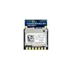


 工商网监
湘ICP备2023018690号
工商网监
湘ICP备2023018690号
