802.15.4
ATSAMR21G18-MR210UA
DATASHEET PRELIMINARY
Description
The ATSAMR21G18-MR210UA is a 20mm x 19mm wireless module with a
solder mount footprint. It integrates an ATSAMR21G18 IC together with a
serial flash and a crypto authentication device.
Features
•
•
•
•
•
•
•
•
•
•
ATSAMR21G18 system in package
®
®
– Single-chip ARM Cortex -M0+ based 32-bit Microcontroller
– Low power 2.4GHz transceiver for IEEE 802.15.4 and ZigBee
applications
– 256KB Flash
– Maximum Operating Frequency: 48 MHz
– 128-bit AES crypto engine
– 32-bit MAC symbol counter
– Temperature sensor
– Automatic transmission modes
AT45DB041E 4-Mbit DataFlash
ATECC508A CryptoAuthentication Device
– Secure Hardware-based Key Storage
– Performs High-Speed Public Key Algorithms
– NIST Standard P256 Elliptic Curve Support
– SHA-256 Hash Algorithm with HMAC Option
– Guaranteed Unique 72-bit Serial Number
– High-quality FIPS Random Number Generator (RNG)
– Intrusion Latch for External Tamper Switch
Single 1.8V - 3.6V supply
Radio module with a link budget of 103dBm
FCC / ETSI compliant RF front end with harmonic filter
Three SERCOM units left for external applications
32.768kHz crystal oscillator
High precision 16MHz crystal oscillator
12-bit, 350ksps Analog-to-Digital Converter (ADC)
Atmel-42475B-ATSAMR21G18-MR210UA_Datasheet_Preliminary-09/2015
�•
•
•
•
I2C up to 3.4MHz
Full-speed (12Mbps) Universal Serial Bus (USB) 2.0 interface
17 external GPIO lines
One GPIO for ATECC508A intrusion latch
Atmel ATSAMR21G18-MR210UA [DATASHEET]
Atmel-42475B-ATSAMR21G18-MR210UA_Datasheet_Preliminary-09/2015
2
�Table of Contents
Description.......................................................................................................................1
Features.......................................................................................................................... 1
1. Integrated Devices and Block Diagram..................................................................... 4
1.1.
1.2.
Module Block Diagram................................................................................................................. 4
Integrated Peripherals.................................................................................................................. 4
1.3.
RF Front End Control................................................................................................................... 5
2. Mechanical Description..............................................................................................7
2.1.
2.2.
Mechanical Dimensions................................................................................................................7
Footprint and Layout Recommendation....................................................................................... 7
3. I/O Pin Assignment.................................................................................................... 9
4. Electrical Characteristics..........................................................................................11
4.1.
4.2.
4.3.
Absolute Maximum Ratings........................................................................................................ 11
Recommended Operating Ratings............................................................................................. 11
Module Performance Data..........................................................................................................11
5. Non-Volatile Memory Information............................................................................ 13
6. Radio Certification................................................................................................... 14
6.1.
6.2.
6.3.
6.4.
United States (FCC)................................................................................................................... 14
Europe (ETSI).............................................................................................................................14
Industry Canada (IC) Compliance Statements...........................................................................15
Approved Antennas....................................................................................................................16
7. Boot Loader............................................................................................................. 17
8. Ordering Information................................................................................................18
9. References.............................................................................................................. 19
10. Revision History.......................................................................................................20
�1.
Integrated Devices and Block Diagram
1.1.
Module Block Diagram
Figure 1-1 Module Block Diagram
ATSAMR21G18-MR210UA
AT45DB041E
U.Fl
50Ohm
SPI
4-Mbit DataFlash
ATSAMR21G18
ARM® Cortex®-M0+
Balun &
Harmonic Filter
Antenna Diversity
Switch
ATECC508
CryptoAuthentication
Device
U.Fl
50Ohm
SWI
17 GPIO
1 GPIO
1.2.
Integrated Peripherals
1.2.1.
Serial Flash Interconnection
Table 1-1 Serial Flash Interconnection
DataFlash Signal
MCU Function
MCU Pin Port and SERCOM Configuration
SO
MISO
37
PA22 SERCOM5 PAD[2] DIPO=0x2
SI
MOSI
38
PA23 SERCOM5 PAD[3] DOPO=0x2
SCK
SCK
48
PB03 SERCOM5 PAD[1] DOPO=0x2
#CS
GPIO
47
PB02 to be set low in software before SPI access
The signals in this table are not available as module I/O. More information about the FLASH IC can be
found in its related datasheet [ADESTO].
1.2.2.
UART with Hardware Flow Control (RTS/CTS)
For an Application where the ADC is not in use, SERCOM0 can be multiplexed as shown in the table
below.
Table 1-2 UART with Hardware Flow Control (RTS/CTS)
Module Pin
MCU Function
MCU Pin
Port and SERCOM Configuration
14
UART TX
15
SERCOM0; MUX=C; PAD[0] TXPO=0x2
25
UART RX
10
SERCOM0; MUX=D; PAD[1] RXPO=0x1
Atmel ATSAMR21G18-MR210UA [DATASHEET]
Atmel-42475B-ATSAMR21G18-MR210UA_Datasheet_Preliminary-09/2015
4
�Module Pin
MCU Function
MCU Pin
Port and SERCOM Configuration
26
UART RTS
11
SERCOM0; MUX=D; PAD[2] TXPO=0x2
13
UART CTS
12
SERCOM0; MUX=D; PAD[3] TXPO=0x2
The signals in this table are not available as module IO. More information about the FLASH IC can be
found in its related datasheet. (ADESTO)
1.2.3.
32kHz Crystal
PA00 and PA01 are used for the 32kHz crystal. This pins are not available as module IO.
1.2.4.
SAM R21 USB Availability
The USB pins are made available as differential pair routed GPIO’s. A base board with the required
connection hardware can support an USB interface.
Table 1-3 SAM R21 USB Availability
Module Pin
Function
MCU Pin
Port Configuration or Xplain Function
19
GPIO or USB_D+
33
PA24: For USB MUX=G
20
SPIO or USB_D-
34
PA25: For USB MUX=G
The module power supply can’t be operated directly from a 5V USB source. The module base board has
to implement the required voltage regulator.
1.3.
RF Front End Control
The antenna diversity signals ANT_DIV_P/N are used to control the diversity switch U4. The signal
ANT_DIV_P is available at the IO ring pin 18 to indicate the antenna currently in use.
In addition at pin 17, the RX_TX indicator signal is available to indicate if the module is currently in
transmit mode.
Atmel ATSAMR21G18-MR210UA [DATASHEET]
Atmel-42475B-ATSAMR21G18-MR210UA_Datasheet_Preliminary-09/2015
5
�Table 1-4 RF Front End Control
RF Front End Signal
MCU Function
MCU Pin
ANT_DIV_P
FECTRL2
21
Port and SERCOM
Configuration
PA12; MUX=F;
F3CFG=DIG1
Available at module pin
18
ANT_DIV_N
FECTRL1
16
PA09; MUX=F;
F1CFG=DIG2
FEM_RX_TX
FECTRL3
22
PA13; MUX=F;
F0CFG=DIG3 for High
active TX indication
F0CFG=DIG4 for Low
active TX indication
Available at module pin
17
Atmel ATSAMR21G18-MR210UA [DATASHEET]
Atmel-42475B-ATSAMR21G18-MR210UA_Datasheet_Preliminary-09/2015
6
�2.
Mechanical Description
2.1.
Mechanical Dimensions
Dimensions are in mm. The module pins are arranged with a 1mm pitch distance. The module is
designed in a symmetric way.
Figure 2-1 Module Bottom Dimensions ( Seen from a CAD top perspective )
The module can be mounted to a base board with a soldered RF connection. For this case one or both
U.Fl connectors are left unconnected and the RF pads on the bottom side are used to feed an antenna
located on the base board.
2.2.
Footprint and Layout Recommendation
Since the module does not contain an antenna, the module does not set any limits for the base board
material selection or the board stack-up construction. The module does also not require a certain
positioning on the board in relation to the board edge. The module must be placed away from interference
sources on the base board like clock oscillators or step converters. The area underneath the module must
be filled with a grounded copper plane. The RF-Pad area needs special attention. The following sections
provide more information on that.
A typical design is supposed to connect the I/O ring to the base board while the antenna feeds are using
the U.Fl connectors. Using the antennas in Approved Antennas on page 16, the modular approval for
the final product can be used without re-certification.
2.2.1.
Design without RF-Pads
For a design without U.Fl connected antennas, the base board design has to have no copper fill within the
RF-Pad area (*!). All layers with less than 0.5mm distance from top shall not be filled with copper
underneath the RF-Pad area.
Atmel ATSAMR21G18-MR210UA [DATASHEET]
Atmel-42475B-ATSAMR21G18-MR210UA_Datasheet_Preliminary-09/2015
7
�For all other I/O pads the geometry in below figure should be used.
Figure 2-2 Recommended Base Board Layout
2.2.2.
Design without RF-Pads
For applications where the antenna is implemented on the base PCB, the RF-Pads can be used to
connect the RF signals. The pad layout is available in Figure 2-2 Recommended Base Board Layout on
page 8. The base board traces shall be designed with a line impedance of 50Ohm. Depending on the
base board stack construction a microstrip or a grounded coplanar design can be implemented. The best
choice will be the line type with the best match in between line width and the 0.8mm pad width.
For all other IO pads the geometry in Figure 2-2 Recommended Base Board Layout on page 8 should be
used.
Atmel ATSAMR21G18-MR210UA [DATASHEET]
Atmel-42475B-ATSAMR21G18-MR210UA_Datasheet_Preliminary-09/2015
8
�3.
I/O Pin Assignment
The module pin assignment is shown in below table. The Column "MCU pin" is referring to the
ATSAMR21G18 datasheet [SAMR21]. The column “Port Configuration” is intended to help determine the
required SAMR21 port configuration..
Table 3-1 RF Front End Control
Module Pin
Function
MCU Pin Port Configuration
1
GND
2
GND
3
VCC
4
VCC
5
RSTN
40
6
SPI_CS
26
SERCOM1; MUX=C; DOPO=0x1; Master PAD1
7
SPI_MOSI
27
SERCOM1; MUX=C; DOPO=0x1 Master PAD2
For slave operation this pin is MISO
8
SPI_MISO
25
SERCOM1; MUX=C; DIPO=0x0 Master PAD0
For slave operation this pin is MOSI
9
SPI_SCLK
28
SERCOM1; MUX=C; DOPO=0x1 Master PAD3
10
GPIO
41
PA28 (Yellow LED; low active)
11
-
12
GND
13
RXD1
Not connected
12
SERCOM0; MUX=D; PAD[3] RXPO=0x3
Can be used for UART with RTS/CTS
14
TXD1
15
SERCOM0; MUX=C; PAD[0] TXPO=0x0
Can be used for UART with RTS/CTS
15
-
Not connected
16
-
Not connected
17
FEM_RX_TX
22
PA13; MUX=F; FECTRL3 (LED red)
18
ANT_DIV_P
21
PA12; MUX=F; FECTRL2 (LED green)
19
GPIO/USB_DM
33
PA24 for USB MUX=G
20
GPIO/USB_DP
34
PA25 for USB MUX=G
21
-
22
RXD0
24
SERCOM2; MUX=C; PAD[3]; RXPO=0x3
23
TXD0
23
SERCOM2; MUX=C; PAD[2]; TXPO=0x1
Not connected
Atmel ATSAMR21G18-MR210UA [DATASHEET]
Atmel-42475B-ATSAMR21G18-MR210UA_Datasheet_Preliminary-09/2015
9
�Module Pin
Function
MCU Pin Port Configuration
24
AREF
9
MUX=B; disable digital
25
ADC0
10
MUX=B; AIN[1]; disable digital
Can be used for UART with RTS/CTS
26
ADC1
11
MUX=B; AIN[2]¸ disable digital
Can be used for UART with RTS/CTS
27
-
Not connected
28
-
Not connected
29
GND
30
SWCLK
45
Programming interface
31
SWDIO
46
Programming interface
32
-
33
ATECC508 GPIO
34
-
Not connected
35
-
Not connected
36
I2C SCL
32
SERCOM3 PAD1 MUX=C
37
I2C SDA
31
SERCOM3 PAD0 MUX=C
38
-
Not connected
39
-
Not connected
40
-
Not connected
41
GND
42
GND
Not connected
Crypto IC GPIO with intrusion detection feature
Atmel ATSAMR21G18-MR210UA [DATASHEET]
Atmel-42475B-ATSAMR21G18-MR210UA_Datasheet_Preliminary-09/2015
10
�4.
Electrical Characteristics
This section will outline the main parameters required to build applications. The module characteristics
are determined by the implemented parts. See References on page 19 for required datasheet
references.
4.1.
Absolute Maximum Ratings
Table 4-1 Absolute Maximum Ratings
Symbol Parameter
Min.
Typ. Max.
Unit
TSTOR
Storage temperature
-40
+125
VPIN
Pin voltage with
respect to GND and
VDD
GND-0.3V
VDD+0.3V V
VESD
ESD robustness
PRF
4.2.
Condition
Modules I/O's
routed to SAM
R21
Human Body
Model
°C
4
kV
Charged
550
Device Model
V
Input RF level
+10
dBm
Recommended Operating Ratings
Table 4-2 Recommended Operating Ratings
4.3.
Symbol
Parameter
Condition
TOP
Operating temperature range
VDD
Supply voltage
Min.
Typ.
Max.
Unit
-40
85
°C
1.8
3.6
V
Module Performance Data
If not otherwise stated the measurements are done with VDD=3.3V at 25°C.
Table 4-3 Module Performance Data
Symbol
Parameter
Condition
Min. Typ. Max. Unit
IDD
Supply current
MCU at TBD MHz(1)
4
With transceiver in RX_ON state
10
With transceiver in TX state
10
PRF
RF transmit power
U.Fl interface
Pemit
Radiated transmit power Using antenna ANT-24G-S21-P5FL(2)
Using antenna
2
M07-FL(3)
mA
3.5
3.5
dBm
8
8
Atmel ATSAMR21G18-MR210UA [DATASHEET]
Atmel-42475B-ATSAMR21G18-MR210UA_Datasheet_Preliminary-09/2015
dBm
EIRP
11
�Symbol
Parameter
Condition
Min. Typ. Max. Unit
PSPUR_TX Transmitter spurious
emissions
U.Fl connector, conducted, >2.5GHz
PSENS
Receiver sensitivity
U.Fl interface
-98
dBm
dod
Outdoor range
Using antenna ANT-24G-S21-P5FL
TBD
m
ANT-24G-S21-P5FL in Ch26(2)
TBD
Using antenna M07-FL
TBD
M07-FL in Ch26(3)
TBD
fRef_0
-50
Reference crystal
deviation
T = 25°C default XTAL_TRIM setting
T = 25°C NV memory XTAL_TRIM setting -5
+5
fRef_T
Reference crystal drift
over temperature
-40°C
ATSAMR21G18-MR210UA 价格&库存
很抱歉,暂时无法提供与“ATSAMR21G18-MR210UA”相匹配的价格&库存,您可以联系我们找货
免费人工找货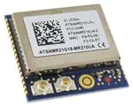


 工商网监
湘ICP备2023018690号
工商网监
湘ICP备2023018690号
