Features
• High-performance, Low-power AVR® 8-bit Microcontroller
• RISC Architecture
•
•
•
•
•
•
•
– 118 Powerful Instructions – Most Single Clock Cycle Execution
– 32 x 8 General Purpose Working Registers
– Fully Static Operation
– Up to 16 MIPS Throughput at 16 MHz
Data and Non-volatile Program Memory
– 2K Bytes of In-System Programmable Program Memory Flash
Endurance: 10,000 Write/Erase Cycles
– 128 Bytes of In-System Programmable EEPROM
Endurance: 100,000 Write/Erase Cycles
– 128 Bytes Internal SRAM
– Programming Lock for Flash Program and EEPROM Data Security
Peripheral Features
– 8-bit Timer/Counter with Separate Prescaler
– 8-bit High-speed Timer with Separate Prescaler
2 High Frequency PWM Outputs with Separate Output Compare Registers
Non-overlapping Inverted PWM Output Pins
– Universal Serial Interface with Start Condition Detector
– 10-bit ADC
11 Single Ended Channels
8 Differential ADC Channels
7 Differential ADC Channel Pairs with Programmable Gain (1x, 20x)
– On-chip Analog Comparator
– External Interrupt
– Pin Change Interrupt on 11 Pins
– Programmable Watchdog Timer with Separate On-chip Oscillator
Special Microcontroller Features
– Low Power Idle, Noise Reduction, and Power-down Modes
– Power-on Reset and Programmable Brown-out Detection
– External and Internal Interrupt Sources
– In-System Programmable via SPI Port
– Internal Calibrated RC Oscillator
I/O and Packages
– 20-lead PDIP/SOIC: 16 Programmable I/O Lines
– 32-lead QFN/MLF: 16 programmable I/O Lines
Operating Voltages
– 2.7V - 5.5V for ATtiny26L
– 4.5V - 5.5V for ATtiny26
Speed Grades
– 0 - 8 MHz for ATtiny26L
– 0 - 16 MHz for ATtiny26
Power Consumption at 1 MHz, 3V and 25°C for ATtiny26L
– Active 16 MHz, 5V and 25°C: Typ 15 mA
– Active 1 MHz, 3V and 25°C: 0.70 mA
– Idle Mode 1 MHz, 3V and 25°C: 0.18 mA
– Power-down Mode: < 1 µA
8-bit
Microcontroller
with 2K Bytes
Flash
ATtiny26
ATtiny26L
Not recommended for new
designs
1477J–AVR–06/07
�Pin Configuration
PDIP/SOIC
(MOSI/DI/SDA/OC1A) PB0
(MISO/DO/OC1A) PB1
(SCK/SCL/OC1B) PB2
(OC1B) PB3
VCC
GND
(ADC7/XTAL1) PB4
(ADC8/XTAL2) PB5
(ADC9/INT0/T0) PB6
(ADC10/RESET) PB7
1
2
3
4
5
6
7
8
9
10
20
19
18
17
16
15
14
13
12
11
PA0 (ADC0)
PA1 (ADC1)
PA2 (ADC2)
PA3 (AREF)
GND
AVCC
PA4 (ADC3)
PA5 (ADC4)
PA6 (ADC5/AIN0)
PA7 (ADC6/AIN1)
32
31
30
29
28
27
26
25
PB2 (SCK/SCL/OC1B)
PB1 (MISO/DO/OC1A)
PB0 (MOSI/DI/SDA/OC1A)
NC
NC
NC
PA0 (ADC0)
PA1 (ADC1)
MLF Top View
24
23
22
21
20
19
18
17
1
2
3
4
5
6
7
8
NC
PA2 (ADC2)
PA3 (AREF)
GND
NC
NC
AVCC
PA4 (ADC3)
NC
(ADC9/INT0/T0) PB6
(ADC10/RESET) PB7
NC
(ADC6/AIN1) PA7
(ADC5/AIN0) PA6
(ADC4) PA5
NC
9
10
11
12
13
14
15
16
NC
(OC1B) PB3
NC
VCC
GND
NC
(ADC7/XTAL1) PB4
(ADC8/XTAL2) PB5
Note:
2
The bottom pad under the QFN/MLF package should be soldered to ground.
ATtiny26(L)
1477J–AVR–06/07
�ATtiny26(L)
Description
The ATtiny26(L) is a low-power CMOS 8-bit microcontroller based on the AVR
enhanced RISC architecture. By executing powerful instructions in a single clock cycle,
the ATtiny26(L) achieves throughputs approaching 1 MIPS per MHz allowing the system
designer to optimize power consumption versus processing speed.
The AVR core combines a rich instruction set with 32 general purpose working registers.
All the 32 registers are directly connected to the Arithmetic Logic Unit (ALU), allowing
two independent registers to be accessed in one single instruction executed in one clock
cycle. The resulting architecture is more code efficient while achieving throughputs up to
ten times faster than conventional CISC microcontrollers. The ATtiny26(L) has a high
precision ADC with up to 11 single ended channels and 8 differential channels. Seven
differential channels have an optional gain of 20x. Four out of the seven differential
channels, which have the optional gain, can be used at the same time. The ATtiny26(L)
also has a high frequency 8-bit PWM module with two independent outputs. Two of the
PWM outputs have inverted non-overlapping output pins ideal for synchronous rectification. The Universal Serial Interface of the ATtiny26(L) allows efficient software
implementation of TWI (Two-wire Serial Interface) or SM-bus interface. These features
allow for highly integrated battery charger and lighting ballast applications, low-end thermostats, and firedetectors, among other applications.
The ATtiny26(L) provides 2K bytes of Flash, 128 bytes EEPROM, 128 bytes SRAM, up
to 16 general purpose I/O lines, 32 general purpose working registers, two 8-bit
Timer/Counters, one with PWM outputs, internal and external Oscillators, internal and
external interrupts, programmable Watchdog Timer, 11-channel, 10-bit Analog to Digital
Converter with two differential voltage input gain stages, and four software selectable
power saving modes. The Idle mode stops the CPU while allowing the Timer/Counters
and interrupt system to continue functioning. The ATtiny26(L) also has a dedicated ADC
Noise Reduction mode for reducing the noise in ADC conversion. In this sleep mode,
only the ADC is functioning. The Power-down mode saves the register contents but
freezes the oscillators, disabling all other chip functions until the next interrupt or hardware reset. The Standby mode is the same as the Power-down mode, but external
oscillators are enabled. The wakeup or interrupt on pin change features enable the
ATtiny26(L) to be highly responsive to external events, still featuring the lowest power
consumption while in the Power-down mode.
The device is manufactured using Atmel’s high density non-volatile memory technology.
By combining an enhanced RISC 8-bit CPU with Flash on a monolithic chip, the
ATtiny26(L) is a powerful microcontroller that provides a highly flexible and cost effective solution to many embedded control applications.
The ATtiny26(L) AVR is supported with a full suite of program and system development
tools including: Macro assemblers, program debugger/simulators, In-circuit emulators,
and evaluation kits.
3
1477J–AVR–06/07
�Block Diagram
Figure 1. The ATtiny26(L) Block Diagram
VCC
8-BIT DATA BUS
INTERNAL
OSCILLATOR
INTERNAL
CALIBRATED
OSCILLATOR
TIMING AND
CONTROL
GND
PROGRAM
COUNTER
STACK
POINTER
WATCHDOG
TIMER
PROGRAM
FLASH
SRAM
MCU CONTROL
REGISTER
AVCC
INSTRUCTION
REGISTER
MCU STATUS
REGISTER
GENERAL
PURPOSE
REGISTERS
TIMER/
COUNTER0
X
Y
Z
INSTRUCTION
DECODER
TIMER/
COUNTER1
CONTROL
LINES
ALU
UNIVERSAL
SERIAL
INTERFACE
STATUS
REGISTER
INTERRUPT
UNIT
ANALOG
COMPARATOR
+
-
PROGRAMMING
LOGIC
DATA REGISTER
PORT A
DATA DIR.
REG.PORT A
PORT A DRIVERS
PA0-PA7
4
EEPROM
ISP INTERFACE
ADC
OSCILLATORS
DATA REGISTER
PORT B
DATA DIR.
REG.PORT B
PORT B DRIVERS
PB0-PB7
ATtiny26(L)
1477J–AVR–06/07
�ATtiny26(L)
Pin Descriptions
VCC
Digital supply voltage pin.
GND
Digital ground pin.
AVCC
AVCC is the supply voltage pin for Port A and the A/D Converter (ADC). It should be
externally connected to VCC, even if the ADC is not used. If the ADC is used, it should be
connected to VCC through a low-pass filter. See page 96 for details on operating of the
ADC.
Port A (PA7..PA0)
Port A is an 8-bit general purpose I/O port. PA7..PA0 are all I/O pins that can provide
internal pull-ups (selected for each bit). Port A has alternate functions as analog inputs
for the ADC and analog comparator and pin change interrupt as described in “Alternate
Port Functions” on page 48.
Port B (PB7..PB0)
Port B is an 8-bit general purpose I/O port. PB6..0 are all I/O pins that can provide internal pull-ups (selected for each bit). PB7 is an I/O pin if not used as the reset. To use pin
PB7 as an I/O pin, instead of RESET pin, program (“0”) RSTDISBL Fuse. Port B has
alternate functions for the ADC, clocking, timer counters, USI, SPI programming, and
pin change interrupt as described in “Alternate Port Functions” on page 48.
An External Reset is generated by a low level on the PB7/RESET pin. Reset pulses
longer than 50 ns will generate a reset, even if the clock is not running. Shorter pulses
are not guaranteed to generate a reset.
XTAL1
Input to the inverting oscillator amplifier and input to the internal clock operating circuit.
XTAL2
Output from the inverting oscillator amplifier.
5
1477J–AVR–06/07
�Resources
6
A comprehensive set of development tools, application notes and datasheets are available for download on http://www.atmel.com/avr.
ATtiny26(L)
1477J–AVR–06/07
�ATtiny26(L)
About Code
Examples
This datasheet contains simple code examples that briefly show how to use various
parts of the device. These code examples assume that the part specific header file is
included before compilation. Be aware that not all C compiler vendors include bit definitions in the header files and interrupt handling in C is compiler dependent. Please
confirm with the C compiler documentation for more details.
7
1477J–AVR–06/07
�AVR CPU Core
Architectural Overview
The fast-access Register File concept contains 32 x 8-bit general purpose working registers with a single clock cycle access time. This means that during one single clock
cycle, one ALU (Arithmetic Logic Unit) operation is executed. Two operands are output
from the Register File, the operation is executed, and the result is stored back in the
Register File – in one clock cycle.
Six of the 32 registers can be used as 16-bit pointers for indirect memory access. These
pointers are called the X-, Y-, and Z-pointers, and they can address the Register File
and the Flash program memory.
Figure 2. The ATtiny26(L) AVR Enhanced RISC Architecture
8-bit Data Bus
Control
Registers
1024 x 16
Program
FLASH
Program
Counter
Status
and Test
32 x 8
General
Purpose
Registers
Instruction
Register
Interrupt
Unit
Universal
Serial Interface
Control Lines
Indirect Addressing
Instruction
Decoder
Direct Addressing
ISP Unit
2 x 8-bit
Timer/Counter
ALU
Watchdog
Timer
128 x 8
SRAM
128 byte
EEPROM
ADC
Analog
Comparator
I/O Lines
The ALU supports arithmetic and logic functions between registers or between a constant and a register. Single register operations are also executed in the ALU. Figure 2
shows the ATtiny26(L) AVR Enhanced RISC microcontroller architecture. In addition to
the register operation, the conventional memory addressing modes can be used on the
Register File as well. This is enabled by the fact that the Register File is assigned the 32
lowermost Data Space addresses ($00 - $1F), allowing them to be accessed as though
they were ordinary memory locations.
The I/O memory space contains 64 addresses for CPU peripheral functions as Control
Registers, Timer/Counters, A/D Converters, and other I/O functions. The I/O Memory
can be accessed directly, or as the Data Space locations following those of the Register
File, $20 - $5F.
8
ATtiny26(L)
1477J–AVR–06/07
�ATtiny26(L)
The AVR uses a Harvard architecture concept with separate memories and buses for
program and data memories. The program memory is accessed with a two stage
pipelining. While one instruction is being executed, the next instruction is pre-fetched
from the program memory. This concept enables instructions to be executed in every
clock cycle. The program memory is In-System programmable Flash memory.
With the relative jump and relative call instructions, the whole address space is directly
accessed. All AVR instructions have a single 16-bit word format, meaning that every
program memory address contains a single 16-bit instruction.
During interrupts and subroutine calls, the return address program counter (PC) is
stored on the Stack. The Stack is effectively allocated in the general data SRAM, and
consequently the stack size is only limited by the total SRAM size and the usage of the
SRAM. All user programs must initialize the SP in the reset routine (before subroutines
or interrupts are executed). The 8-bit Stack Pointer SP is read/write accessible in the I/O
space. For programs written in C, the stack size must be declared in the linker file. Refer
to the C user guide for more information.
The 128 bytes data SRAM can be easily accessed through the five different addressing
modes supported in the AVR architecture.
The memory spaces in the AVR architecture are all linear and regular memory maps.
The I/O memory space contains 64 addresses for CPU peripheral functions as Control
Registers, Timer/Counters, and other I/O functions. The memory spaces in the AVR
architecture are all linear and regular memory maps.
A flexible interrupt module has its control registers in the I/O space with an additional
Global Interrupt Enable bit in the Status Register. All the different interrupts have a separate Interrupt Vector in the Interrupt Vector table at the beginning of the program
memory. The different interrupts have priority in accordance with their Interrupt Vector
position. The lower the Interrupt Vector address, the higher the priority.
General Purpose
Register File
Figure 3 shows the structure of the 32 general purpose working registers in the CPU.
Figure 3. AVR CPU General Purpose Working Registers
7
0
Addr.
R0
$00
R1
$01
R2
$02
…
R13
$0D
General
R14
$0E
Purpose
R15
$0F
Working
R16
$10
Registers
R17
$11
…
R26
$1A
X-register Low Byte
R27
$1B
X-register High Byte
R28
$1C
Y-register Low Byte
R29
$1D
Y-register High Byte
R30
$1E
Z-register Low Byte
R31
$1F
Z-register High Byte
9
1477J–AVR–06/07
�All of the register operating instructions in the instruction set have direct and single cycle
access to all registers. The only exceptions are the five constant arithmetic and logic
instructions SBCI, SUBI, CPI, ANDI, and ORI between a constant and a register, and
the LDI instruction for load immediate constant data. These instructions apply to the
second half of the registers in the Register File – R16..R31. The general SBC, SUB, CP,
AND, and OR, and all other operations between two registers or on a single register
apply to the entire Register File.
As shown in Figure 3, each register is also assigned a data memory address, mapping
them directly into the first 32 locations of the user Data Space. Although not being physically implemented as SRAM locations, this memory organization provides flexibility in
access of the registers, as the X-, Y-, and Z-registers can be set to index any register in
the file.
X-register, Y-register, and Zregister
The registers R26..R31 have some added functions to their general purpose usage.
These registers are address pointers for indirect addressing of the Data Space. The
three indirect address registers X, Y, and Z are defined as:
Figure 4. X-, Y-, and Z-register
15
X-register
7
0
0
R27 ($1B)
7
15
Y-register
7
0
0
R29 ($1D)
7
7
R31 ($1F)
0
R28 ($1C)
15
Z-register
0
R26 ($1A)
0
0
7
0
R30 ($1E)
In the different addressing modes, these address registers have functions as fixed displacement, automatic increment and decrement (see the descriptions for the different
instructions).
ALU – Arithmetic Logic
Unit
10
The high-performance AVR ALU operates in direct connection with all 32 general purpose working registers. Within a single clock cycle, ALU operations between registers in
the Register File are executed. The ALU operations are divided into three main categories – Arithmetic, Logical, and Bit-functions.
ATtiny26(L)
1477J–AVR–06/07
�ATtiny26(L)
Status Register – SREG
The AVR Status Register – SREG – at I/O space location $3F is defined as:
Bit
7
6
5
4
3
2
1
0
$3F ($5F)
I
T
H
S
V
N
Z
C
Read/Write
R/W
R/W
R/W
R/W
R/W
R/W
R/W
R/W
Initial Value
0
0
0
0
0
0
0
0
SREG
• Bit 7 – I: Global Interrupt Enable
The Global Interrupt Enable bit must be set (one) for the interrupts to be enabled. The
individual interrupt enable control is then performed in the Interrupt Mask Registers –
GIMSK and TIMSK. If the Global Interrupt Enable Register is cleared (zero), none of the
interrupts are enabled independent of the GIMSK and TIMSK values. The I-bit is cleared
by hardware after an interrupt has occurred, and is set by the RETI instruction to enable
subsequent interrupts. The I-bit can also be set and cleared by the application with the
SEI and CLI instructions, as described in the instruction set reference.
• Bit 6 – T: Bit Copy Storage
The Bit Copy instructions BLD (Bit LoaD) and BST (Bit STore) use the T-bit as source
and destination for the operated bit. A bit from a register in the Register File can be copied into T by the BST instruction, and a bit in T can be copied into a bit in a register in the
Register File by the BLD instruction.
• Bit 5 – H: Half Carry Flag
The Half Carry Flag H indicates a Half Carry in some arithmetic operations. See the
Instruction Set Description for detailed information.
• Bit 4 – S: Sign Bit, S = N ⊕ V
The S-bit is always an exclusive or between the Negative Flag N and the Two’s Complement Overflow Flag V. See the Instruction Set Description for detailed information.
• Bit 3 – V: Two’s Complement Overflow Flag
The Two’s Complement Overflow Flag V supports two’s complement arithmetics. See
the Instruction Set Description for detailed information.
• Bit 2 – N: Negative Flag
The Negative Flag N indicates a negative result after the different arithmetic and logic
operations. See the Instruction Set Description for detailed information.
• Bit 1 – Z: Zero Flag
The Zero Flag Z indicates a zero result after the different arithmetic and logic operations. See the Instruction Set Description for detailed information.
• Bit 0 – C: Carry Flag
The Carry Flag C indicates a carry in an arithmetic or logic operation. See the Instruction
Set Description for detailed information.
11
1477J–AVR–06/07
�Stack Pointer – SP
The ATtiny26(L) Stack Pointer is implemented as an 8-bit register in the I/O space location $3D ($5D). As the ATtiny26(L) data memory has 224 ($E0) locations, eight bits are
used.
Bit
7
6
5
4
3
2
1
0
$3D ($5D)
SP7
SP6
SP5
SP4
SP3
SP2
SP1
SP0
Read/Write
R/W
R/W
R/W
R/W
R/W
R/W
R/W
R/W
Initial Value
0
0
0
0
0
0
0
0
SP
The Stack Pointer points to the data SRAM stack area where the Subroutine and Interrupt Stacks are located. This Stack space in the data SRAM must be defined by the
program before any subroutine calls are executed or interrupts are enabled. The Stack
Pointer must be set to point above $60. The Stack Pointer is decremented by one when
data is pushed onto the Stack with the PUSH instruction, and it is decremented by two
when an address is pushed onto the Stack with subroutine calls and interrupts. The
Stack Pointer is incremented by one when data is popped from the Stack with the POP
instruction, and it is incremented by two when an address is popped from the Stack with
return from subroutine RET or return from interrupt RETI.
Program and Data
Addressing Modes
The ATtiny26(L) AVR Enhanced RISC microcontroller supports powerful and efficient
addressing modes for access to the Flash program memory, SRAM, Register File, and
I/O Data memory. This section describes the different addressing modes supported by
the AVR architecture. In the figures, OP means the operation code part of the instruction
word. To simplify, not all figures show the exact location of the addressing bits.
Register Direct, Single
Register Rd
Figure 5. Direct Single Register Addressing
The operand is contained in register d (Rd).
12
ATtiny26(L)
1477J–AVR–06/07
�ATtiny26(L)
Register Direct, Two Registers
Rd and Rr
Figure 6. Direct Register Addressing, Two Registers
Operands are contained in register r (Rr) and d (Rd). The result is stored in register d
(Rd).
I/O Direct
Figure 7. I/O Direct Addressing
Operand address is contained in 6 bits of the instruction word. n is the destination or
source register address.
Data Direct
Figure 8. Direct Data Addressing
Data Space
20 19
31
OP
16
$0000
Rr/Rd
16 LSBs
15
0
$00DF
13
1477J–AVR–06/07
�A 16-bit Data Address is contained in the 16 LSBs of a two-word instruction. Rd/Rr
specify the destination or source register.
Data Indirect with
Displacement
Figure 9. Data Indirect with Displacement
Data Space
$0000
15
0
Y OR Z - REGISTER
15
10
OP
6 5
n
0
a
$00DF
Operand address is the result of the Y- or Z-register contents added to the address contained in 6 bits of the instruction word.
Data Indirect
Figure 10. Data Indirect Addressing
Data Space
$0000
15
0
X-, Y-, OR Z-REGISTER
$00DF
Operand address is the contents of the X-, Y-, or the Z-register.
Data Indirect with Predecrement
Figure 11. Data Indirect Addressing with Pre-decrement
Data Space
$0000
15
0
X-, Y-, OR Z-REGISTER
-1
$00DF
14
ATtiny26(L)
1477J–AVR–06/07
�ATtiny26(L)
The X-, Y-, or Z-register is decremented before the operation. Operand address is the
decremented contents of the X-, Y-, or Z-register.
Data Indirect with Postincrement
Figure 12. Data Indirect Addressing with Post-increment
Data Space
$0000
15
0
X-, Y-, OR Z-REGISTER
1
$00DF
The X-, Y-, or Z-register is incremented after the operation. Operand address is the content of the X-, Y-, or Z-register prior to incrementing.
Constant Addressing Using
the LPM Instruction
Figure 13. Code Memory Constant Addressing
PROGRAM MEMORY
$000
$3FF
Constant byte address is specified by the Z-register contents. The 15 MSBs select word
address (0 - 1K), the LSB selects low byte if cleared (LSB = 0) or high byte if set
(LSB = 1).
15
1477J–AVR–06/07
�Indirect Program Addressing,
IJMP and ICALL
Figure 14. Indirect Program Memory Addressing
PROGRAM MEMORY
$000
$3FF
Program execution continues at address contained by the Z-register (i.e., the PC is
loaded with the contents of the Z-register).
Relative Program Addressing,
RJMP and RCALL
Figure 15. Relative Program Memory Addressing
PROGRAM MEMORY
$000
+1
$3FF
Program execution continues at address PC + k + 1. The relative address k is from
-2048 to 2047.
16
ATtiny26(L)
1477J–AVR–06/07
�ATtiny26(L)
Memories
The AVR CPU is driven by the System Clock Ø, directly generated from the external
clock crystal for the chip. No internal clock division is used.
Figure 16 shows the parallel instruction fetches and instruction executions enabled by
the Harvard architecture and the fast-access Register File concept. This is the basic
pipelining concept to obtain up to 1 MIPS per MHz with the corresponding unique results
for functions per cost, functions per clocks, and functions per power-unit.
Figure 16. The Parallel Instruction Fetches and Instruction Executions
T1
T2
T3
T4
System Clock Ø
1st Instruction Fetch
1st Instruction Execute
2nd Instruction Fetch
2nd Instruction Execute
3rd Instruction Fetch
3rd Instruction Execute
4th Instruction Fetch
Figure 17 shows the internal timing concept for the Register File. In a single clock cycle
an ALU operation using two register operands is executed, and the result is stored back
to the destination register.
Figure 17. Single Cycle ALU Operation
T1
T2
T3
T4
System Clock Ø
Total Execution Time
Register Operands Fetch
ALU Operation Execute
Result Write Back
The internal data SRAM access is performed in two System Clock cycles as described
in Figure 18.
17
1477J–AVR–06/07
�Figure 18. On-chip Data SRAM Access Cycles
T1
T2
T3
T4
System Clock Ø
Address
Prev. Address
Address
Write
Data
WR
Read
Data
RD
In-System Programmable The ATtiny26(L) contains 2K bytes On-chip In-System Programmable Flash memory for
program storage. Since all instructions are 16- or 32-bit words, the Flash is organized as
Flash Program Memory
1K x 16. The Flash memory has an endurance of at least 10,000 write/erase cycles. The
ATtiny26(L) Program Counter – PC – is 10 bits wide, thus addressing the 1024 program
memory addresses, see “Memory Programming” on page 109 for a detailed description
on Flash data downloading. See “Program and Data Addressing Modes” on page 12 for
the different program memory addressing modes.
Figure 19. SRAM Organization
Register File
Data Address Space
R0
$0000
R1
$0001
R2
$0002
...
...
R29
$001D
R30
$001E
R31
$001F
I/O Registers
$00
$0020
$01
$0021
$02
$0022
…
…
$3D
$005D
$3E
$005E
$3F
$005F
Internal SRAM
$0060
$0061
...
$00DE
$00DF
SRAM Data Memory
Figure 19 above shows how the ATtiny26(L) SRAM Memory is organized.
The lower 224 Data Memory locations address the Register File, the I/O Memory and
the internal data SRAM. The first 96 locations address the Register File and I/O Memory, and the next 128 locations address the internal data SRAM.
18
ATtiny26(L)
1477J–AVR–06/07
�ATtiny26(L)
The five different addressing modes for the data memory cover: Direct, Indirect with Displacement, Indirect, Indirect with Pre-decrement, and Indirect with Post-increment. In
the Register File, registers R26 to R31 feature the indirect addressing pointer registers.
The direct addressing reaches the entire data space. The Indirect with Displacement
mode features a 63 address locations reach from the base address given by the Y- or Zregister.
When using register indirect addressing modes with automatic pre-decrement and postincrement, the address registers X, Y, and Z are decremented and incremented.
The 32 general purpose working registers, 64 I/O Registers and the 128 bytes of internal data SRAM in the ATtiny26(L) are all accessible through all these addressing
modes.
See “Program and Data Addressing Modes” on page 12 for a detailed description of the
different addressing modes.
EEPROM Data Memory
The ATtiny26(L) contains 128 bytes of data EEPROM memory. It is organized as a separate data space, in which single bytes can be read and written (see “Memory
Programming” on page 109). The EEPROM has an endurance of at least 100,000
write/erase cycles per location.
EEPROM Read/Write Access
The EEPROM Access Registers are accessible in the I/O space.
The write access time is typically 8.3 ms. A self-timing function lets the user software
detect when the next byte can be written. A special EEPROM Ready Interrupt can be
set to trigger when the EEPROM is ready to accept new data.
An ongoing EEPROM write operation will complete even if a reset condition occurs.
In order to prevent unintentional EEPROM writes, a two state write procedure must be
followed. Refer to the description of the EEPROM Control Register for details on this.
When the EEPROM is written, the CPU is halted for two clock cycles before the next
instruction is executed.
When the EEPROM is read, the CPU is halted for four clock cycles before the next
instruction is executed.
EEPROM Address Register –
EEAR
Bit
7
6
5
4
3
2
1
0
$1E ($3E)
–
EEAR6
EEAR5
EEAR4
EEAR3
EEAR2
EEAR1
EEAR0
Read/Write
R
R/W
R/W
R/W
R/W
R/W
R/W
R/W
Initial Value
0
X
X
X
X
X
X
X
EEAR
• Bit 7 – RES: Reserved Bits
This bit are reserved bit in the ATtiny26(L) and will always read as zero.
• Bit 6..0 – EEAR6..0: EEPROM Address
The EEPROM Address Register – EEAR – specifies the EEPROM address in the 128
bytes EEPROM space. The EEPROM data bytes are addressed linearly between 0 and
127. The initial value of EEAR is undefined. A proper value must be written before the
EEPROM may be accessed.
19
1477J–AVR–06/07
�EEPROM Data Register –
EEDR
Bit
7
6
5
4
3
2
1
0
$1D ($3D)
MSB
LSB
Read/Write
R/W
R/W
R/W
R/W
R/W
R/W
R/W
R/W
Initial Value
0
0
0
0
0
0
0
0
EEDR
• Bit 7..0 – EEDR7..0: EEPROM Data
For the EEPROM write operation, the EEDR Register contains the data to be written to
the EEPROM in the address given by the EEAR Register. For the EEPROM read operation, the EEDR contains the data read out from the EEPROM at the address given by
EEAR.
EEPROM Control Register –
EECR
Bit
7
6
5
4
3
2
1
0
$1C ($3C)
–
–
–
–
EERIE
EEMWE
EEWE
EERE
Read/Write
R
R
R
R
R/W
R/W
R/W
R/W
Initial Value
0
0
0
0
0
0
0
0
EECR
• Bit 7..4 – RES: Reserved Bits
These bits are reserved bits in the ATtiny26(L) and will always read as zero.
• Bit 3 – EERIE: EEPROM Ready Interrupt Enable
When the I-bit in SREG and EERIE are set (one), the EEPROM Ready Interrupt is
enabled. When cleared (zero), the interrupt is disabled. The EEPROM Ready Interrupt
generates a constant interrupt when EEWE is cleared (zero).
• Bit 2 – EEMWE: EEPROM Master Write Enable
The EEMWE bit determines whether setting EEWE to one causes the EEPROM to be
written. When EEMWE is set (one), setting EEWE will write data to the EEPROM at the
selected address. If EEMWE is zero, setting EEWE will have no effect. When EEMWE
has been set (one) by software, hardware clears the bit to zero after four clock cycles.
See the description of the EEWE bit for an EEPROM write procedure.
• Bit 1 – EEWE: EEPROM Write Enable
The EEPROM Write Enable Signal – EEWE – is the write strobe to the EEPROM. When
address and data are correctly set up, the EEWE bit must be set to write the value in to
the EEPROM. The EEMWE bit must be set when the logical one is written to EEWE,
otherwise no EEPROM write takes place. The following procedure should be followed
when writing the EEPROM (the order of steps 2 and 3 is unessential):
1. Wait until EEWE becomes zero.
2. Write new EEPROM address to EEAR (optional).
3. Write new EEPROM data to EEDR (optional).
4. Write a logical one to the EEMWE bit in EECR.
5. Within four clock cycles after setting EEMWE, write a logical one to EEWE.
Caution: An interrupt between step 4 and step 5 will make the write cycle fail, since the
EEPROM Master Write Enable will time-out. If an interrupt routine accessing the
EEPROM is interrupting another EEPROM access, the EEAR or EEDR Register will be
modified, causing the interrupted EEPROM access to fail. It is recommended to have
the Global Interrupt Flag cleared during all the steps to avoid these problems.
When the access time (typically 8.3 ms) has elapsed, the EEWE bit is cleared (zero) by
hardware. The user software can poll this bit and wait for a zero before writing the next
byte. When EEWE has been set, the CPU is halted for two cycles before the next
instruction is executed.
20
ATtiny26(L)
1477J–AVR–06/07
�ATtiny26(L)
• Bit 0 – EERE: EEPROM Read Enable
The EEPROM Read Enable Signal – EERE – is the read strobe to the EEPROM. When
the correct address is set up in the EEAR Register, the EERE bit must be set. When the
EERE bit is cleared (zero) by hardware, requested data is found in the EEDR Register.
The EEPROM read access takes one instruction and there is no need to poll the EERE
bit. When EERE has been set, the CPU is halted for four cycles before the next instruction is executed.
The user should poll the EEWE bit before starting the read operation. If a write operation
is in progress when new data or address is written to the EEPROM I/O Registers, the
write operation will be interrupted, and the result is undefined.
Table 1. EEPROM Programming Time
Symbol
EEPROM Write (from CPU)
Note:
Number of Calibrated RC
Oscillator Cycles(1)
Typical Programming
Time
8448
8.5 ms
1. Uses 1 MHz clock, independent of CKSEL-Fuse settings.
EEPROM Write During Powerdown Sleep Mode
When entering Power-down sleep mode while an EEPROM write operation is active, the
EEPROM write operation will continue, and will complete before the write access time
has passed. However, when the write operation is completed, the crystal Oscillator continues running, and as a consequence, the device does not enter Power-down entirely.
It is therefore recommended to verify that the EEPROM write operation is completed
before entering Power-down.
Preventing EEPROM
Corruption
During periods of low VCC, the EEPROM data can be corrupted because the supply voltage is too low for the CPU and the EEPROM to operate properly. These issues are the
same as for board level systems using the EEPROM, and the same design solutions
should be applied.
An EEPROM data corruption can be caused by two situations when the voltage is too
low. First, a regular write sequence to the EEPROM requires a minimum voltage to
operate correctly. Secondly, the CPU itself can execute instructions incorrectly, if the
supply voltage for executing instructions is too low.
EEPROM data corruption can easily be avoided by following these design recommendations (one is sufficient):
1. Keep the AVR RESET active (low) during periods of insufficient power supply
voltage. This can be done by enabling the internal Brown-out Detector (BOD) if
the operating voltage matches the detection level. If not, an external Brown-out
Reset Protection circuit can be applied.
2. Keep the AVR core in Power-down Sleep mode during periods of low VCC. This
will prevent the CPU from attempting to decode and execute instructions, effectively protecting the EEPROM Registers from unintentional writes.
Store constants in Flash memory if the ability to change memory contents from software
is not required. Flash memory can not be updated by the CPU, and will not be subject to
corruption.
21
1477J–AVR–06/07
�I/O Memory
The I/O space definition of the ATtiny26(L) is shown in Table 2
Table 2. ATtiny26(L) I/O Space(1)
22
Address Hex
Name
Function
$3F ($5F)
SREG
Status Register
$3D ($5D)
SP
$3B ($5B)
GIMSK
General Interrupt Mask Register
$3A ($5A)
GIFR
General Interrupt Flag Register
$39 ($59)
TIMSK
Timer/Counter Interrupt Mask Register
$38 ($58)
TIFR
Timer/Counter Interrupt Flag Register
$35 ($55)
MCUCR
MCU Control Register
$34 ($54)
MCUSR
MCU Status Register
$33 ($53)
TCCR0
Timer/Counter0 Control Register
$32 ($52)
TCNT0
Timer/Counter0 (8-bit)
$31 ($51)
OSCCAL
Oscillator Calibration Register
$30 ($50)
TCCR1A
Timer/Counter1 Control Register A
$2F ($4F)
TCCR1B
Timer/Counter1 Control Register B
$2E ($4E)
TCNT1
Timer/Counter1 (8-bit)
$2D ($4D)
OCR1A
Timer/Counter1 Output Compare Register A
$2C ($4C)
OCR1B
Timer/Counter1 Output Compare Register B
$2B ($4B)
OCR1C
Timer/Counter1 Output Compare Register C
$29 ($29)
PLLCSR
PLL Control and Status Register
$21 ($41)
WDTCR
Watchdog Timer Control Register
$1E ($3E)
EEAR
EEPROM Address Register
$1D ($3D)
EEDR
EEPROM Data Register
$1C ($3C)
EECR
EEPROM Control Register
$1B ($3B)
PORTA
Data Register, Port A
$1A ($3A)
DDRA
Data Direction Register, Port A
$19 ($39)
PINA
Input Pins, Port A
$18 ($38)
PORTB
Data Register, Port B
$17 ($37)
DDRB
Data Direction Register, Port B
$16 ($36)
PINB
Input Pins, Port B
$0F ($2F)
USIDR
Universal Serial Interface Data Register
$0E ($2E)
USISR
Universal Serial Interface Status Register
$0D ($2D)
USICR
Universal Serial Interface Control Register
$08 ($28)
ACSR
Analog Comparator Control and Status Register
$07 ($27)
ADMUX
Stack Pointer
ADC Multiplexer Select Register
ATtiny26(L)
1477J–AVR–06/07
�ATtiny26(L)
Table 2. ATtiny26(L) I/O Space(1) (Continued)
Address Hex
Name
$06($26)
ADCSR
$05($25)
ADCH
ADC Data Register High
$04($24)
ADCL
ADC Data Register Low
Note:
Function
ADC Control and Status Register
1. Reserved and unused locations are not shown in the table.
All ATtiny26(L) I/O and peripheral registers are placed in the I/O space. The I/O locations are accessed by the IN and OUT instructions transferring data between the 32
general purpose working registers and the I/O space. I/O Registers within the address
range $00 - $1F are directly bit-accessible using the SBI and CBI instructions. In these
registers, the value of single bits can be checked by using the SBIS and SBIC instructions. Refer to the instruction set chapter for more details. For compatibility with future
devices, reserved bits should be written zero if accessed. Reserved I/O memory
addresses should never be written.
23
1477J–AVR–06/07
�System Clock and
Clock Options
Clock Systems and their
Distribution
Figure 20 presents the principal clock systems in the AVR and their distribution. All of
the clocks need not be active at a given time. In order to reduce power consumption, the
clocks to modules not being used can be halted by using different sleep modes, as
described in “Power Management and Sleep Modes” on page 38. The clock systems
are detailed below.
Figure 20. Clock Distribution
Timer/Counter1
General I/O
modules
ADC
CPU Core
Flash and
EEPROM
RAM
clkADC
clkI/O
AVR Clock
Control Unit
clkCPU
clkFLASH
Reset Logic
Source clock
Watchdog clock
Clock
Multiplexer
clkPCK
Watchdog Timer
Watchdog
Oscillator
clkPLL
PLL
External RC
Oscillator
External clock
Crystal
Oscillator
Low-Frequency
Crystal Oscillator
Calibrated RC
Oscillator
CPU Clock – clkCPU
The CPU clock is routed to parts of the system concerned with operation of the AVR
core. Examples of such modules are the General Purpose Register File, the Status Register and the data memory holding the Stack Pointer. Halting the CPU clock inhibits the
core from performing general operations and calculations.
I/O Clock – clkI/O
The I/O clock is used by the majority of the I/O modules, like Timer/Counters, and USI.
The I/O clock is also used by the External Interrupt module, but note that some external
interrupts are detected by asynchronous logic, allowing such interrupts to be detected
even if the I/O clock is halted.
Flash Clock – clkFLASH
The Flash clock controls operation of the Flash interface. The Flash clock is usually
active simultaneously with the CPU clock.
ADC Clock – clkADC
The ADC is provided with a dedicated clock domain. This allows halting the CPU and
I/O clocks in order to reduce noise generated by digital circuitry. This gives more accurate ADC conversion results.
24
ATtiny26(L)
1477J–AVR–06/07
�ATtiny26(L)
Internal PLL for Fast
Peripheral Clock Generation –
clkPCK
The internal PLL in ATtiny26(L) generates a clock frequency that is 64x multiplied from
nominally 1 MHz input. The source of the 1 MHz PLL input clock is the output of the
internal RC Oscillator which is automatically divided down to 1 MHz, if needed. See the
Figure 21 on page 25. When the PLL reference frequency is the nominal 1 MHz, the fast
peripheral clock is 64 MHz. The fast peripheral clock, or a clock prescaled from that, can
be selected as the clock source for Timer/Counter1.
The PLL is locked on the RC Oscillator and adjusting the RC Oscillator via OSCCAL
Register will adjust the fast peripheral clock at the same time. However, even if the possibly divided RC Oscillator is taken to a higher frequency than 1 MHz, the fast peripheral
clock frequency saturates at 70 MHz (worst case) and remains oscillating at the maximum frequency. It should be noted that the PLL in this case is not locked any more with
the RC Oscillator clock.
Therefore it is recommended not to take the OSCCAL adjustments to a higher frequency than 1 MHz in order to keep the PLL in the correct operating range. The internal
PLL is enabled only when the PLLE bit in the register PLLCSR is set or the PLLCK Fuse
is programmed (“0”). The bit PLOCK from the register PLLCSR is set when PLL is
locked.
Both internal 1 MHz RC Oscillator and PLL are switched off in Power-down and Standby
sleep modes.
Figure 21. PCK Clocking System
PLLE
PLLCK &
CKSEL
FUSES
OSCCAL
PLOCK
Lock
Detector
1
RC OSCILLATOR 2
4
8 MHz
DIVIDE
TO 1 MHz
PCK
PLL
64x
DIVIDE
BY 4
CK
XTAL1
XTAL2
OSCILLATORS
25
1477J–AVR–06/07
�Clock Sources
The device has the following clock source options, selectable by Flash Fuse bits as
shown below on Table 3. The clock from the selected source is input to the AVR clock
generator, and routed to the appropriate modules.The use of pins PB5 (XTAL2), and
PB4 (XTAL1) as I/O pins is limited depending on clock settings, as shown below in
Table 4.
Table 3. Device Clocking Options Select
Device Clocking Option
PLLCK
CKSEL3..0
External Crystal/Ceramic Resonator
1
1111 - 1010
External Low-frequency Crystal
1
1001
External RC Oscillator
1
1000 - 0101
Calibrated Internal RC Oscillator
1
0100 - 0001
External Clock
1
0000
PLL Clock
0
0001
Table 4. PB5, and PB4 Functionality vs. Device Clocking Options(1)
Device Clocking Option
PLLCK
CKSEL [3:0]
PB4
PB5
External Clock
1
0000
XTAL1
I/O
Internal RC Oscillator
1
0001
I/O
I/O
Internal RC Oscillator
1
0010
I/O
I/O
Internal RC Oscillator
1
0011
I/O
I/O
Internal RC Oscillator
1
0100
I/O
I/O
External RC Oscillator
1
0101
XTAL1
I/O
External RC Oscillator
1
0110
XTAL1
I/O
External RC Oscillator
1
0111
XTAL1
I/O
External RC Oscillator
1
1000
XTAL1
I/O
External Low-frequency Oscillator
1
1001
XTAL1
XTAL2
External Crystal/Resonator Oscillator
1
1010
XTAL1
XTAL2
External Crystal/Resonator Oscillator
1
1011
XTAL1
XTAL2
External Crystal/Resonator Oscillator
1
1100
XTAL1
XTAL2
External Crystal/Resonator Oscillator
1
1101
XTAL1
XTAL2
External Crystal/Resonator Oscillator
1
1110
XTAL1
XTAL2
External Crystal/Resonator Oscillator
1
1111
XTAL1
XTAL2
PLL
0
0001
I/O
I/O
Note:
1. For all fuses “1” means unprogrammed while “0” means programmed.
The various choices for each clocking option is given in the following sections. When the
CPU wakes up from Power-down, the selected clock source is used to time the start-up,
ensuring stable oscillator operation before instruction execution starts. When the CPU
starts from Reset, there is as an additional delay allowing the power to reach a stable
level before commencing normal operation. The Watchdog Oscillator is used for timing
this real-time part of the start-up time. The number of WDT Oscillator cycles used for
26
ATtiny26(L)
1477J–AVR–06/07
�ATtiny26(L)
each time-out is shown in Table 5. The frequency of the Watchdog Oscillator is voltage
dependent as shown in the Electrical Characteristics section.
Table 5. Number of Watchdog Oscillator Cycles
Typ Time-out (VCC = 5.0V)
Typ Time-out (VCC = 3.0V)
Number of Cycles
4.1 ms
4.3 ms
4K (4,096)
65 ms
69 ms
64K (65,536)
Default Clock Source
The deviced is shipped with CKSEL = “0001”, SUT = “10”, and PLLCK unprogrammed.
The default clock source setting is therefore the internal RC Oscillator with longest startup time. This default setting ensures that all users can make their desired clock source
setting using an In-System or Parallel Programmer.
Crystal Oscillator
XTAL1 and XTAL2 are input and output, respectively, of an inverting amplifier which can
be configured for use as an On-chip Oscillator, as shown in Figure 22. Either a quartz
crystal or a ceramic resonator may be used. The maximum frequency for resonators is
12 MHz. The CKOPT Fuse should always be unprogrammed when using this clock
option. C1 and C2 should always be equal. The optimal value of the capacitors depends
on the crystal or resonator in use, the amount of stray capacitance, and the electromagnetic noise of the environment. Some initial guidelines for choosing capacitors for use
with crystals are given in Table 6. For ceramic resonators, the capacitor values given by
the manufacturer should be used.
Figure 22. Crystal Oscillator Connections
C2
XTAL2
C1
XTAL1
GND
The Oscillator can operate in three different modes, each optimized for a specific frequency range. The operating mode is selected by the fuses CKSEL3..1 as shown in
Table 6.
Table 6. Crystal Oscillator Operating Modes
CKSEL3..1
Frequency
Range (MHz)
Recommended Range for Capacitors C1 and
C2 for Use with Crystals (pF)
101(1)
0.4 - 0.9
–
110
0.9 - 3.0
12 - 22
3.0 - 16
12 - 22
16 -
12 - 15
111
Note:
1. This option should not be used with crystals, only with ceramic resonators.
27
1477J–AVR–06/07
�The CKSEL0 Fuse together with the SUT1..0 Fuses select the start-up times as shown
in Table 7.
Table 7. Start-up Times for the Crystal Oscillator Clock Selection
CKSEL0
SUT1..0
Start-up Time
from Power-down
Additional Delay from
Reset (VCC = 5.0V)
0
00
258 CK(1)
4.1 ms
Ceramic resonator,
fast rising power
0
01
258 CK(1)
65 ms
Ceramic resonator,
slowly rising power
0
10
1K CK(2)
–
Ceramic resonator,
BOD enabled
0
11
1K CK(2)
4.1 ms
Ceramic resonator,
fast rising power
1
00
1K CK(2)
65 ms
Ceramic resonator,
slowly rising power
1
01
16K CK
–
1
10
16K CK
4.1 ms
Crystal Oscillator, fast
rising power
1
11
16K CK
65 ms
Crystal Oscillator,
slowly rising power
Notes:
Low-frequency Crystal
Oscillator
Recommended
Usage
Crystal Oscillator,
BOD enabled
1. These options should only be used when not operating close to the maximum frequency of the device, and only if frequency stability at start-up is not important for the
application.
2. These options are intended for use with ceramic resonators and will ensure frequency stability at start-up. They can also be used with crystals when not operating
close to the maximum frequency of the device, and if frequency stability at start-up is
not important for the application.
To use a 32.768 kHz watch crystal as the clock source for the device, the Low-frequency Crystal Oscillator must be selected by setting the PLLCK to “1” and CKSEL
Fuses to “1001”. The crystal should be connected as shown in Figure 22. By programming the CKOPT Fuse, the user can enable internal capacitors on XTAL1 and XTAL2,
thereby removing the need for external capacitors. The internal capacitors have a nominal value of 36 pF.
When this oscillator is selected, start-up times are determined by the SUT Fuses as
shown in Table 8.
Table 8. Start-up Times for the Low-frequency Crystal Oscillator Clock Selection
SUT1..0
Additional Delay from
Reset (VCC = 5.0V)
Recommended Usage
(1)
4.1 ms
Fast rising power or BOD enabled
01
(1)
1K CK
65 ms
Slowly rising power
10
32K CK
65 ms
Stable frequency at start-up
00
11
Note:
28
Start-up Time
from Power-down
1K CK
Reserved
1. These options should only be used if frequency stability at start-up is not important
for the application.
ATtiny26(L)
1477J–AVR–06/07
�ATtiny26(L)
External RC Oscillator
For timing insensitive applications, the external RC configuration shown in Figure 23
can be used. The frequency is roughly estimated by the equation f = 1/(3RC). C should
be at least 22 pF. By programming the CKOPT Fuse, the user can enable an internal
36 pF capacitor between XTAL1 and GND, thereby removing the need for an external
capacitor.
Figure 23. External RC Configuration
VCC
PB5 (XTAL2)
R
XTAL1
C
GND
The oscillator can operate in four different modes, each optimized for a specific frequency range. The operating mode is selected by the fuses CKSEL3..0 as shown in
Table 9.
Table 9. External RC Oscillator Operating Modes
CKSEL3..0
Frequency Range (MHz)
0101
0.1 - 0.9
0110
0.9 - 3.0
0111
3.0 - 8.0
1000
8.0 - 12.0
When this oscillator is selected, start-up times are determined by the SUT Fuses as
shown in Table 10.
Table 10. Start-up Times for the External RC Oscillator Clock Selection
SUT1..0
Start-up Time
from Power-down
Additional Delay from
Reset (VCC = 5.0V)
00
18 CK
–
01
18 CK
4.1 ms
Fast rising power
10
18 CK
65 ms
Slowly rising power
11
(1)
4.1 ms
Fast rising power or BOD enabled
Notes:
6 CK
Recommended Usage
BOD enabled
1. This option should not be used when operating close to the maximum frequency of
the device.
29
1477J–AVR–06/07
�Calibrated Internal RC
Oscillator
The calibrated internal RC Oscillator provides a fixed 1.0, 2.0, 4.0, or 8.0 MHz clock. All
frequencies are nominal values at 5V and 25°C. This clock may be selected as the system clock by programming the CKSEL Fuses as shown in Table 11. If selected, it will
operate with no external components. The CKOPT Fuse should always be unprogrammed when using this clock option. During Reset, hardware loads the calibration
byte into the OSCCAL Register and thereby automatically calibrates the RC Oscillator.
At 5V, 25°C and 1.0 MHz Oscillator frequency selected, this calibration gives a frequency within ± 3% of the nominal frequency. Using run-time calibration methods as
described in application notes available at www.atmel.com/avr it is possible to achieve ±
1% accuracy at any given VCC and Temperature. When this oscillator is used as the chip
clock, the Watchdog Oscillator will still be used for the Watchdog Timer and for the reset
time-out. For more information on the pre-programmed calibration value, see the section
“Calibration Byte” on page 111.
Table 11. Internal Calibrated RC Oscillator Operating Modes
CKSEL3..0
Nominal Frequency (MHz)
(1)
1.0
0001
Note:
0010
2.0
0011
4.0
0100
8.0
1. The device is shipped with this option selected.
When this oscillator is selected, start-up times are determined by the SUT Fuses as
shown in Table 12. PB4 (XTAL1) and PB5 (XTAL2) can be used as general I/O ports.
Table 12. Start-up Times for the Internal Calibrated RC Oscillator Clock Selection
SUT1..0
Start-up Time from
Power-down
Additional Delay from
Reset (VCC = 5.0V)
00
6 CK
–
01
6 CK
4.1 ms
Fast rising power
6 CK
65 ms
Slowly rising power
(1)
10
11
Note:
Oscillator Calibration Register
– OSCCAL
Recommended Usage
BOD enabled
Reserved
1. The device is shipped with this option selected.
Bit
$31 ($51)
Read/Write
Initial Value
7
6
5
4
3
2
1
0
CAL7
CAL6
CAL5
CAL4
CAL3
CAL2
CAL1
CAL0
R/W
R/W
R/W
R/W
R/W
R/W
R/W
R/W
OSCCAL
Device Specific Calibration Value
• Bits 7..0 – CAL7..0: Oscillator Calibration Value
Writing the calibration byte to this address will trim the internal oscillator to remove process variations from the oscillator frequency. During Reset, the 1 MHz calibration value
which is located in the signature row high byte (address 0x00) is automatically loaded
into the OSCCAL Register. If the internal RC is used at other frequencies, the calibration
value must be loaded manually. This can be done by first reading the signature row by a
programmer, and then store the calibration values in the Flash or EEPROM. Then the
value can be read by software and loaded into the OSCCAl Register. When OSCCAL is
zero, the lowest available frequency is chosen. Writing non-zero values to this register
30
ATtiny26(L)
1477J–AVR–06/07
�ATtiny26(L)
will increase the frequency of the internal oscillator. Writing $FF to the register gives the
highest available frequency. The calibrated Oscillator is used to time EEPROM and
Flash access. If EEPROM or Flash is written, do not calibrate to more than 10% above
the nominal frequency. Otherwise, the EEPROM or Flash write may fail. Note that the
oscillator is intended for calibration to 1.0, 2.0, 4.0, or 8.0 MHz. Tuning to other values is
not guaranteed, as indicated in Table 13.
Table 13. Internal RC Oscillator Frequency Range.
External Clock
OSCCAL Value
Min Frequency in Percentage of
Nominal Frequency
Max Frequency in Percentage of
Nominal Frequency
$00
50%
100%
$7F
75%
150%
$FF
100%
200%
To drive the device from an external clock source, XTAL1 should be driven as shown in
Figure 24. To run the device on an external clock, the CKSEL Fuses must be programmed to “0000” and PLLCK to “1”. By programming the CKOPT Fuse, the user can
enable an internal 36 pF capacitor between XTAL1 and GND.
Figure 24. External Clock Drive Configuration
PB5 (XTAL2)
EXTERNAL
CLOCK
SIGNAL
XTAL1
GND
When this clock source is selected, start-up times are determined by the SUT Fuses as
shown in Table 14.
Table 14. Start-up Times for the External Clock Selection
SUT1..0
Start-up Time from
Power-down
Additional Delay from
Reset (VCC = 5.0V)
00
6 CK
–
01
6 CK
4.1 ms
Fast rising power
10
6 CK
65 ms
Slowly rising power
11
Recommended Usage
BOD enabled
Reserved
When applying an external clock, it is required to avoid sudden changes in the applied
clock frequency to ensure stable operation of the MCU. A variation in frequency of more
than 2% from one clock cycle to the next can lead to unpredictable behaviour. It is
required to ensure that the MCU is kept in reset during such changes in the clock
frequency.
31
1477J–AVR–06/07
�High Frequency PLL
Clock – PLLCLK
There is an internal PLL that provides nominally 64 MHz clock rate locked to the RC
Oscillator for the use of the Peripheral Timer/Counter1 and for the system clock source.
When selected as a system clock source, by programming (“0”) the fuse PLLCK, it is
divided by four. When this option is used, the CKSEL3..0 must be set to “0001”. This
clocking option can be used only when operating between 4.5 - 5.5V to guaratee safe
operation. The system clock frequency will be 16 MHz (64 MHz/4). When using this
clock option, start-up times are determined by the SUT Fuses as shown in Table 15.
See also “PCK Clocking System” on page 25.
Table 15. Start-up Times for the PLLCK
32
SUT1..0
Start-up Time from
Power-down
Additional Delay from
Reset (VCC = 5.0V)
00
1K CK
–
01
1K CK
4.1 ms
Fast rising power
10
1K CK
65 ms
Slowly rising power
11
16K CK
–
Slowly rising power
Recommended Usage
BOD enabled
ATtiny26(L)
1477J–AVR–06/07
�ATtiny26(L)
System Control and
Reset
The ATtiny26(L) provides four sources of reset:
• Power-on Reset. The MCU is reset when the supply voltage is below the Power-on Reset
threshold (VPOT).
• External Reset. To use the PB7/RESET pin as an External Reset, instead of I/O pin,
unprogram (“1”) the RSTDISBL Fuse. The MCU is reset when a low level is present on the
RESET pin for more than 500 ns.
• Watchdog Reset. The MCU is reset when the Watchdog timer period expires and the
Watchdog is enabled.
• Brown-out Reset. The MCU is reset when the supply voltage VCC is below the Brown-out
Reset threshold (VBOT).
During reset, all I/O Registers are then set to their initial values, and the program starts
execution from address $000. The instruction placed in address $000 must be an RJMP
– Relative Jump – instruction to the reset handling routine. If the program never enables
an interrupt source, the interrupt vectors are not used, and regular program code can be
placed at these locations. Figure 25 shows the reset logic for the ATtiny26(L). Table 16
shows the timing and electrical parameters of the reset circuitry for ATtiny26(L).
Figure 25. Reset Logic for the ATtiny26(L)
DATA BUS
PORF
BORF
EXTRF
WDRF
MCU Status
Register (MCUSR)
BODEN
BODLEVEL
Brown-Out
Reset Circuit
Clock
Generator
CK
Delay Counters
TIMEOUT
CKSEL[3:0]
33
1477J–AVR–06/07
�Table 16. Reset Characteristics
Symbol
VPOT
Parameter
Condition
Min
Typ
Max
Units
Power-on Reset Threshold
Voltage (rising)
1.4
2.3
V
Power-on Reset Threshold
Voltage (falling)(1)
1.3
2.3
V
0.9
VCC
1.5
µs
VRST
RESET Pin Threshold Voltage
tRST
Minimum pulse width on
RESET Pin
Brown-out Reset Threshold
Voltage(2)
BODLEVEL = 1
2.4
2.7
2.9
VBOT
BODLEVEL = 0
3.7
4.0
4.5
Minimum low voltage period for
Brown-out Detection
BODLEVEL = 1
2
µs
tBOD
BODLEVEL = 0
2
µs
VHYST
Brown-out Detector hysteresis
130
mV
Notes:
0.2
V
1. The Power-on Reset will not work unless the supply voltage has been below VPOT
(falling)
2. VBOT may be below nominal minimum operating voltage for some devices. For
devices where this is the case, the device is tested down to VCC = VBOT during the
production test. This guarantees that a Brown-out Reset will occur before VCC drops
to a voltage where correct operation of the microcontroller is no longer guaranteed.
The test is performed using BODLEVEL=1 for ATtiny26L and BODLEVEL=0 for
ATtiny26. BODLEVEL=1 is not applicable for ATtiny26.
See start-up times from reset from “System Clock and Clock Options” on page 24.
When the CPU wakes up from Power-down, only the clock counting part of the start-up
time is used. The Watchdog Oscillator is used for timing the real-time part of the start-up
time.
Power-on Reset
A Power-on Reset (POR) pulse is generated by an On-chip Detection circuit. The detection level is defined in Table 16 The POR is activated whenever V CC is below the
detection level. The POR circuit can be used to trigger the Start-up Reset, as well as
detect a failure in supply voltage.
The Power-on Reset (POR) circuit ensures that the device is reset from Power-on.
Reaching the Power-on Reset threshold voltage invokes a delay counter, which determines the delay, for which the device is kept in RESET after V CC rise. The time-out
period of the delay counter can be defined by the user through the CKSEL Fuses. The
different selections for the delay period are presented in “System Clock and Clock
Options” on page 24. The RESET signal is activated again, without any delay, when the
VCC decreases below detection level.
34
ATtiny26(L)
1477J–AVR–06/07
�ATtiny26(L)
Figure 26. MCU Start-up, RESET Tied to VCC
VCC
RESET
VPOT
VRST
tTOUT
TIME-OUT
INTERNAL
RESET
Figure 27. MCU Start-up, RESET Controlled Externally
VCC
VPOT
VRST
RESET
tTOUT
TIME-OUT
INTERNAL
RESET
External Reset
An External Reset is generated by a low level on the RESET pin. Reset pulses longer
than 500 ns will generate a reset, even if the clock is not running. Shorter pulses are not
guaranteed to generate a reset. When the applied signal reaches the Reset Threshold
Voltage – VRST – on its positive edge, the delay timer starts the MCU after the Time-out
period tTOUT has expired.
Figure 28. External Reset During Operation
VCC
RESET
VRST
t TOUT
TIME-OUT
INTERNAL
RESET
35
1477J–AVR–06/07
�Brown-out Detection
ATtiny26(L) has an On-chip Brown-out Detection (BOD) circuit for monitoring the VCC
level during the operation. The BOD circuit can be enabled/disabled by the fuse
BODEN. When the BOD is enabled (BODEN programmed), and VCC decreases below
the trigger level, the Brown-out Reset is immediately activated. When VCC increases
above the trigger level, the Brown-out Reset is deactivated after a delay. The delay is
defined by the user in the same way as the delay of POR signal, in Table 29. The trigger
level for the BOD can be selected by the fuse BODLEVEL to be 2.7V (BODLEVEL
unprogrammed), or 4.0V (BODLEVEL programmed). The trigger level has a hysteresis
of 50 mV to ensure spike free Brown-out Detection.
The BOD circuit will only detect a drop in VCC if the voltage stays below the trigger level
for longer than tBOD given in Table 16.
Figure 29. Brown-out Reset During Operation
VCC
VBOT-
VBOT+
RESET
tTOUT
TIME-OUT
INTERNAL
RESET
Watchdog Reset
When the Watchdog times out, it will generate a short reset pulse of one CK cycle duration. On the falling edge of this pulse, the delay timer starts counting the Time-out period
tTOUT. Refer to page 80 for details on operation of the Watchdog.
Figure 30. Watchdog Time-out
1 CK Cycle
36
ATtiny26(L)
1477J–AVR–06/07
�ATtiny26(L)
MCU Status Register –
MCUSR
Bit
7
6
5
4
3
2
1
0
$34 ($54)
–
–
–
–
WDRF
BORF
EXTRF
PORF
Read/Write
R
R
R
R
R/W
R/W
R/W
R/W
Initial Value
0
0
0
0
MCUSR
See Bit Description
• Bit 7..4 – Res: Reserved Bits
These bits are reserved bits in the ATtiny26(L) and always read as zero.
• Bit 3 – WDRF: Watchdog Reset Flag
This bit is set (one) if a Watchdog Reset occurs. The bit is reset (zero) by a Power-on
Reset, or by writing a logic zero to the flag.
• Bit 2 – BORF: Brown-out Reset Flag
This bit is set (one) if a Brown-out Reset occurs. The bit is reset (zero) by a Power-on
Reset, or by writing a logic zero to the flag.
• Bit 1 – EXTRF: External Reset Flag
This bit is set (one) if an External Reset occurs. The bit is reset (zero) by a Power-on
Reset, or by writing a logic zero to the flag.
• Bit 0 – PORF: Power-on Reset Flag
This bit is set (one) if a Power-on Reset occurs. The bit is reset (zero) by writing a logic
zero to the flag.
To make use of the reset flags to identify a reset condition, the user should read and
then reset (zero) the MCUSR as early as possible in the program. If the register is
cleared before another reset occurs, the source of the reset can be found by examining
the reset flags.
37
1477J–AVR–06/07
�Power Management
and Sleep Modes
Sleep modes enable the application to shut down unused modules in the MCU, thereby
saving power. The AVR provides various sleep modes allowing the user to tailor the
power consumption to the application’s requirements.
To enter any of the four sleep modes, the SE bit in MCUCR must be written to logic one
and a SLEEP instruction must be executed. The SM1, and SM0 bits in the MCUCR
Register select which sleep mode (Idle, ADC Noise Reduction, Power Down, or Standby) will be activated by the SLEEP instruction. See Table 17 for a summary. If an
enabled interrupt occurs while the MCU is in a sleep mode, the MCU wakes up. The
MCU is then halted for four cycles in addition to the start-up time, it executes the interrupt routine, and resumes execution from the instruction following SLEEP. The contents
of the Register File and SRAM are unaltered when the device wakes up from sleep. If a
Reset occurs during sleep mode, the MCU wakes up and executes from the Reset
Vector.
Table 19 on page 40 presents the different clock systems in the ATtiny26, and their distribution. The figure is helpful in selecting an appropriate sleep mode.
MCU Control Register –
MCUCR
The MCU Control Register contains control bits for general MCU functions.
Bit
7
6
5
4
3
2
1
0
$35 ($55)
–
PUD
SE
SM1
SM0
–
ISC01
ISC00
Read/Write
R
R/W
R/W
R/W
R/W
R
R/W
R/W
Initial Value
0
0
0
0
0
0
0
0
MCUCR
• Bits 7 – Res: Reserved Bit
This bit is a reserved bit in the ATtiny26(L) and always reads as zero.
• Bit 6 – PUD: Pull-up Disable
When this bit is set (one), the pull-ups in the I/O ports are disabled even if the DDxn and
PORTxn Registers are configured to enable the pull-ups ({DDxn, PORTxn} = 0b01). See
“Configuring the Pin” on page 44 for more details about this feature.
• Bit 5 – SE: Sleep Enable
The SE bit must be set (one) to make the MCU enter the Sleep mode when the SLEEP
instruction is executed. To avoid the MCU entering the Sleep mode unless it is the programmers purpose, it is recommended to set the Sleep Enable SE bit just before the
execution of the SLEEP instruction.
• Bits 4,3 – SM1/SM0: Sleep Mode Select Bits 1 and 0
These bits select between the four available Sleep modes, as shown in the following
table.
Table 17. Sleep Modes
SM1
SM0
Sleep Mode
0
0
Idle mode
0
1
ADC Noise Reduction mode
1
0
Power-down mode
1
1
Standby mode
For details, refer to the paragraph “Sleep Modes” below.
• Bit 2 – Res: Reserved Bit
This bit is a reserved bit in the ATtiny26(L) and always reads as zero.
38
ATtiny26(L)
1477J–AVR–06/07
�ATtiny26(L)
• Bits 1, 0 – ISC01, ISC00: Interrupt Sense Control 0 Bit 1 and Bit 0
The External Interrupt 0 is activated by the external pin INT0 if the SREG I-flag and the
corresponding interrupt mask is set (one). The activity on the external INT0 pin that activates the interrupt is defined in the following table.
Table 18. Interrupt 0 Sense Control(1)
ISC01
ISC00
0
0
The low level of INT0 generates an interrupt request.
0
1
Any change on INT0 generates an interrupt request.
1
0
The falling edge of INT0 generates an interrupt request.
1
1
The rising edge of INT0 generates an interrupt request.
Note:
Idle Mode
Description
1. When changing the ISC10/ISC00 bits, INT0 must be disabled by clearing its Interrupt
Enable bit in the GIMSK Register. Otherwise an interrupt can occur when the bits are
changed.
When the SM1..0 bits are written to “00”, the SLEEP instruction makes the MCU enter
Idle mode, stopping the CPU but allowing Analog Comparator, ADC, USI,
Timer/Counters, Watchdog, and the interrupt system to continue operating. This sleep
mode basically halts clkCPU and clkFLASH, while allowing the other clocks to run.
Idle mode enables the MCU to wake up from external triggered interrupts as well as
internal ones like the Timer Overflow and USI Start and Overflow interrupts. If wake-up
from the Analog Comparator interrupt is not required, the Analog Comparator can be
powered down by setting the ACD bit in the Analog Comparator Control and Status
Register – ACSR. This will reduce power consumption in Idle mode. If the ADC is
enabled, a conversion starts automatically when this mode is entered.
ADC Noise Reduction
Mode
When the SM1..0 bits are written to “01”, the SLEEP instruction makes the MCU enter
ADC Noise Reduction mode, stopping the CPU but allowing the ADC, the External Interrupts, the USI start condition detection, and the Watchdog to continue operating (if
enabled). This sleep mode basically halts clkI/O, clkCPU, and clkFLASH, while allowing the
other clocks to run.
This improves the noise environment for the ADC, enabling higher resolution measurements. If the ADC is enabled, a conversion starts automatically when this mode is
entered. Apart form the ADC Conversion Complete interrupt, only an External Reset, a
Watchdog Reset, a Brown-out Reset, USI start condition interrupt, an EEPROM ready
interrupt, an External Level Interrupt on INT0, or a pin change interrupt can wake up the
MCU from ADC Noise Reduction mode.
Power-down Mode
When the SM1..0 bits are written to “10”, the SLEEP instruction makes the MCU enter
Power-down mode. In this mode, the External Oscillator is stopped, while the External
Interrupts, the USI start condition detection, and the Watchdog continue operating (if
enabled). Only an External Reset, a Watchdog Reset, a Brown-out Reset, USI start condition interrupt, an External Level Interrupt on INT0, or a pin change interrupt can wake
up the MCU. This sleep mode basically halts all generated clocks, allowing operation of
asynchronous modules only.
When waking up from Power-down mode, there is a delay from the wake-up condition
occurs until the wake-up becomes effective. This allows the clock to restart and become
stable after having been stopped. The wake-up period is defined by the same CKSEL
Fuses that define the reset time-out period, as described in “Clock Sources” on page 26.
39
1477J–AVR–06/07
�Note that if a level triggered external interrupt or pin change interrupt is used from
Power-down mode, the changed level must be held for some time to wake up the MCU.
This makes the MCU less sensitive to noise.
If the wake-up condition disappears before the MCU wakes up and starts to execute,
e.g., a low level on INT0 is not held long enough, the interrupt causing the wake-up will
not be executed.
Standby Mode
When the SM1..0 bits are “11” and an External Crystal/Resonator clock option is
selected, the SLEEP instruction forces the MCU into the Standby mode. This mode is
identical to Power-down with the exception that the Oscillator is kept running. From
Standby mode, the device wakes up in only six clock cycles.
Table 19. Active Clock Domains and Wake-up Sources in the different Sleep Modes.
Active Clock domains
Sleep Mode
clkCPU
clkFLASH
Idle
ADC Noise
Reduction
Oscillators
clkIO
clkADC
Main Clock
Source Enabled
INT0, and Pin
Change
USI Start
Condition
EEPROM
Ready
ADC
Other I/O
X
X
X
X
X
X
X
X
X
X
X(2)
X
X
X
(2)
X
X
X(2)
X
Power-down
Standby(1)
Notes:
40
Wake-up Sources
X
1. Only recommended with external crystal or resonator selected as clock source.
2. Only level interrupt INT0.
ATtiny26(L)
1477J–AVR–06/07
�ATtiny26(L)
Minimizing Power
Consumption
There are several issues to consider when trying to minimize the power consumption in
an AVR controlled system. In general, sleep modes should be used as much as possible, and the sleep mode should be selected so that as few as possible of the device’s
functions are operating. All functions not needed should be disabled. In particular, the
following modules may need special consideration when trying to achieve the lowest
possible power consumption.
Analog to Digital Converter
If enabled, the ADC will be enabled in all sleep modes. To save power, the ADC should
be disabled before entering any sleep mode. When the ADC is turned off and on again,
the next conversion will be an extended conversion. Refer to “Analog to Digital Converter” on page 96 for details on ADC operation.
Analog Comparator
When entering Idle mode, the Analog Comparator should be disabled if not used. When
entering ADC Noise Reduction mode, the Analog Comparator should be disabled. In the
other sleep modes, the Analog Comparator is automatically disabled. However, if the
Analog Comparator is set up to use the Internal Voltage Reference as input, the Analog
Comparator should be disabled in all sleep modes. Otherwise, the Internal Voltage Reference will be enabled, independent of sleep mode. Refer to “Analog Comparator” on
page 93 for details on how to configure the Analog Comparator.
Brown-out Detector
If the Brown-out Detector is not needed in the application, this module should be turned
off. If the Brown-out Detector is enabled by the BODEN Fuse, it will be enabled in all
sleep modes, and hence, always consume power. In the deeper sleep modes, this will
contribute significantly to the total current consumption. Refer to “Brown-out Detection”
on page 36 for details on how to configure the Brown-out Detector.
Internal Voltage Reference
The Internal Voltage Reference (see Table 20) will be enabled when needed by the
Brown-out Detector, the Analog Comparator or the ADC. If these modules are disabled
as described in the sections above, the Internal Voltage Reference will be disabled and
it will not be consuming power. When turned on again, the user must allow the reference
to start up before the output is used. If the reference is kept on in sleep mode, the output
can be used immediately.
Table 20. Internal Voltage Reference
Symbol
Parameter
Min
Typ
Max
Units
VBG
Bandgap reference voltage
1.15
1.18
1.40
V
tBG
Bandgap reference start-up time
40
70
µs
IBG
Bandgap reference current consumption
10
µA
Watchdog Timer
If the Watchdog Timer is not needed in the application, this module should be turned off.
If the Watchdog Timer is enabled, it will be enabled in all sleep modes, and hence,
always consume power. In the deeper sleep modes, this will contribute significantly to
the total current consumption. Refer to “Watchdog Timer” on page 80 for details on how
to configure the Watchdog Timer.
Port Pins
When entering a sleep mode, all port pins should be configured to use minimum power.
The most important thing is then to ensure that no pins drive resistive loads. In sleep
modes where the both the I/O clock (clkI/O) and the ADC clock (clkADC) are stopped, the
input buffers of the device will be disabled. This ensures that no power is consumed by
the input logic when not needed. In some cases, the input logic is needed for detecting
wake-up conditions, and it will then be enabled. Refer to “Digital Input Enable and Sleep
Modes” on page 47 for details on which pins are enabled. If the input buffer is enabled
41
1477J–AVR–06/07
�and the input signal is left floating or have an analog signal level close to VCC/2, the
input buffer will use excessive power.
42
ATtiny26(L)
1477J–AVR–06/07
�ATtiny26(L)
I/O Ports
Introduction
All AVR ports have true Read-Modify-Write functionality when used as general digital
I/O ports. This means that the direction of one port pin can be changed without unintentionally changing the direction of any other pin with the SBI and CBI instructions. The
same applies when changing drive value (if configured as output) or enabling/disabling
of pull-up resistors (if configured as input). Each output buffer, except reset, has symmetrical drive characteristics with both high sink and source capability. The pin driver is
strong enough to drive LED displays directly. All port pins have individually selectable
pull-up resistors with a supply-voltage invariant resistance. All I/O pins have protection
diodes to both VCC and Ground as indicated in Figure 31.
Figure 31. I/O Pin Equivalent Schematic
Rpu
Logic
Pxn
Cpin
See Figure
"General Digital I/O" for
Details
All registers and bit references in this section are written in general form. A lower case
“x” represents the numbering letter for the port, and a lower case “n” represents the bit
number. However, when using the register or bit defines in a program, the precise form
must be used. For example, PORTB3 for bit no. 3 in Port B, here documented generally
as PORTxn. The physical I/O Registers and bit locations are listed in “Register Description for I/O Ports” on page 58.
Three I/O memory address locations are allocated for each port, one each for the Data
Register – PORTx, Data Direction Register – DDRx, and the Port Input Pins – PINx. The
Port Input Pins I/O location is read only, while the Data Register and the Data Direction
Register are read/write. In addition, the Pull-up Disable – PUD bit in MCUCR disables
the pull-up function for all pins in all ports when set.
Using the I/O port as General Digital I/O is described in “Ports as General Digital I/O” on
page 44. Most port pins are multiplexed with alternate functions for the peripheral features on the device. How each alternate function interferes with the port pin is described
in “Alternate Port Functions” on page 48. Refer to the individual module sections for a
full description of the alternate functions.
Note that enabling the alternate function of some of the port pins does not affect the use
of the other pins in the port as general digital I/O.
43
1477J–AVR–06/07
�Ports as General Digital
I/O
The ports are bi-directional I/O ports with optional internal pull-ups. Figure 32 shows a
functional description of one I/O-port pin, here generically called Pxn.
Figure 32. General Digital I/O(1)
PUD
Q
D
DDxn
Q CLR
RESET
WDx
Q
Pxn
D
PORTxn
Q CLR
WPx
DATA BUS
RDx
RESET
RRx
SLEEP
SYNCHRONIZER
D
Q
L
Q
D
RPx
Q
PINxn
Q
clk I/O
PUD:
SLEEP:
clkI/O:
Note:
Configuring the Pin
PULLUP DISABLE
SLEEP CONTROL
I/O CLOCK
WDx:
RDx:
WPx:
RRx:
RPx:
WRITE DDRx
READ DDRx
WRITE PORTx
READ PORTx REGISTER
READ PORTx PIN
1. WPx, WDx, RRx, RPx, and RDx are common to all pins within the same port. clkI/O,
SLEEP, and PUD are common to all ports.
Each port pin consists of 3 Register bits: DDxn, PORTxn, and PINxn. As shown in “Register Description for I/O Ports” on page 58, the DDxn bits are accessed at the DDRx I/O
address, the PORTxn bits at the PORTx I/O address, and the PINxn bits at the PINx I/O
address.
The DDxn bit in the DDRx Register selects the direction of this pin. If DDxn is written
logic one, Pxn is configured as an output pin. If DDxn is written logic zero, Pxn is configured as an input pin.
If PORTxn is written logic one when the pin is configured as an input pin, the pull-up
resistor is activated. To switch the pull-up resistor off, PORTxn has to be written logic
zero or the pin has to be configured as an output pin. The port pins are tri-stated when a
reset condition becomes active, even if no clocks are running.
If PORTxn is written logic one when the pin is configured as an output pin, the port pin is
driven high (one). If PORTxn is written logic zero when the pin is configured as an output pin, the port pin is driven low (zero).
When switching between tri-state ({DDxn, PORTxn} = 0b00) and output high ({DDxn,
PORTxn} = 0b11), an intermediate state with either pull-up enabled ({DDxn, PORTxn} =
0b01) or output low ({DDxn, PORTxn} = 0b10) must occur. Normally, the pull-up
enabled state is fully acceptable, as a high-impedant environment will not notice the
44
ATtiny26(L)
1477J–AVR–06/07
�ATtiny26(L)
difference between a strong high driver and a pull-up. If this is not the case, the PUD bit
in the MCUCR Register can be set to disable all pull-ups in all ports.
Switching between input with pull-up and output low generates the same problem. The
user must use either the tri-state ({DDxn, PORTxn} = 0b00) or the output high state
({DDxn, PORTxn} = 0b11) as an intermediate step.
Table 21 summarizes the control signals for the pin value.
Table 21. Port Pin Configurations
Reading the Pin Value
DDxn
PORTxn
PUD
(in MCUCR)
I/O
Pull-up
0
0
X
Input
No
Tri-state (Hi-Z)
0
1
0
Input
Yes
Pxn will source current if ext. pulled
low
0
1
1
Input
No
Tri-state (Hi-Z)
1
0
X
Output
No
Output Low (Sink)
1
1
X
Output
No
Output High (Source)
Comment
Independent of the setting of Data Direction bit DDxn, the port pin can be read through
the PINxn Register Bit. As shown in Figure 32, the PINxn Register bit and the preceding
latch constitute a synchronizer. This is needed to avoid metastability if the physical pin
changes value near the edge of the internal clock, but it also introduces a delay. Figure
33 shows a timing diagram of the synchronization when reading an externally applied
pin value. The maximum and minimum propagation delays are denoted tpd,max and tpd,min
respectively.
Figure 33. Synchronization when Reading an Externally Applied Pin Value
SYSTEM CLK
INSTRUCTIONS
XXX
XXX
in r17, PINx
SYNC LATCH
PINxn
r17
0x00
0xFF
t pd, max
t pd, min
Consider the clock period starting shortly after the first falling edge of the system clock.
The latch is closed when the clock is low, and goes transparent when the clock is high,
as indicated by the shaded region of the “SYNC LATCH” signal. The signal value is
latched when the system clock goes low. It is clocked into the PINxn Register at the succeeding positive clock edge. As indicated by the two arrows tpd,max and tpd,min, a single
45
1477J–AVR–06/07
�signal transition on the pin will be delayed between ½ and 1½ system clock period
depending upon the time of assertion.
When reading back a software assigned pin value, a nop instruction must be inserted as
indicated in Figure 34. The out instruction sets the “SYNC LATCH” signal at the positive
edge of the clock. In this case, the delay tpd through the synchronizer is one system
clock period.
Figure 34. Synchronization when Reading a Software Assigned Pin Value
SYSTEM CLK
r16
INSTRUCTIONS
0xFF
out PORTx, r16
nop
in r17, PINx
SYNC LATCH
PINxn
r17
0x00
0xFF
t pd
46
ATtiny26(L)
1477J–AVR–06/07
�ATtiny26(L)
The following code example shows how to set port B pins 0 and 1 high, 2 and 3 low, and
define the port pins from 4 to 7 as input with pull-ups assigned to port pins 6 and 7. The
resulting pin values are read back again, but as previously discussed, a nop instruction
is included to be able to read back the value recently assigned to some of the pins.
Assembly Code Example(1)
...
; Define pull-ups and set outputs high
; Define directions for port pins
ldi
r16,(1
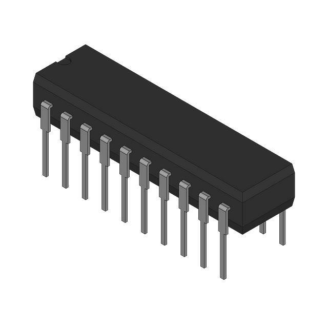


 工商网监
湘ICP备2023018690号
工商网监
湘ICP备2023018690号
