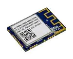
ATWINC1500-MR210PB1172 数据手册
ATWINC15x0
ATWINC15x0-MR210xB IEEE® 802.11 b/g/n SmartConnect
IoT Module
Introduction
The ATWINC15x0-MR210xB is a low power consumption 802.11 b/g/n IoT (Internet of Things) module, specifically
optimized for low power IoT applications. The module integrates Power Amplifier (PA), Low-Noise Amplifier (LNA),
Switch, Power Management and a printed antenna or a micro co-ax (U.FL) connector for an external antenna
resulting in a small form factor (21.7 x 14.7 x 2.1 mm) design. It is interoperable with various vendors’ 802.11 b/g/n
access points. This module provides Serial Peripheral Interface (SPI) ports to interface with a host controller.
The references to the ATWINC15x0-MR210xB module include the module devices listed in the following:
• ATWINC1500-MR210PB
• ATWINC1500-MR210UB
• ATWINC1510-MR210PB
• ATWINC1510-MR210UB
Features
•
•
•
•
•
•
•
•
•
•
•
•
•
•
•
•
•
•
•
IEEE® 802.11 b/g/n 20 MHz (1x1) solution
Single spatial stream in 2.4 GHz ISM band
Integrated Transmit/Receive switch
Integrated PCB antenna or U.FL micro co-ax connector for external antenna
Superior sensitivity and range via advanced PHY signal processing
Advanced equalization and channel estimation
Advanced carrier and timing synchronization
Wi-Fi® Direct (supported till firmware release 19.5.2)
Soft-AP support
Supports IEEE 802.11 WEP, WPA, WPA2 security
Support Enterprise security with WPA/WPA2 (802.1X)(1)
– EAP-TLS
– EAP-PEAPv0/1 with TLS
– EAP-TTLSv0 with MSCHAPv2
– EAP-PEAPv0/1 with MSCHAPv2
Superior MAC throughput via hardware accelerated two-level A-MSDU/A-MPDU frame aggregation and block
acknowledgment
On-chip memory management engine to reduce host load
SPI host interface
Operating temperature range from -40°C to +85°C. RF performance at room temperature of 25oC with a 2-3 dB
change at boundary conditions
Power supply for I/O (VDDIO) rages from 2.7V to 3.6V
Power supply for DC/DC converter (VBAT) ranges from 3.0V to 4.2V
Built-in 26 MHz crystal
Integrated Flash memory for system software
© 2015-2021 Microchip Technology Inc.
Datasheet
DS70005304E-page 1
�ATWINC15x0
•
•
•
•
•
•
•
Power Save modes
– 4 µA Power-Down mode typical at 3.3V I/O
– 380 µA Doze mode with chip settings preserved (used for beacon monitoring) (2)
– On-chip low power sleep oscillator
– Fast host wake-up from Doze mode by a pin or SPI transaction
Fast Boot options
– On-chip boot ROM (Firmware instant boot)
– SPI flash boot
– Low-leakage on-chip memory for state variables
– Fast AP re-association (150 ms)
On-chip Network stack to offload MCU
– Network features TCP, UDP, DHCP, ARP, HTTP, TLS and DNS
– Hardware accelerators for Wi-Fi and TLS security to improve connection time
Hardware accelerator for IP checksum
Hardware accelerators for OTA security
Small footprint host driver
Wi-Fi Alliance® certifications for Connectivity and Optimizations
– ID: WFA61069
Notes:
1. For more information on the software features, refer to the Wi-Fi Network Controller Software Design Guide at
ww1.microchip.com/downloads/en/DeviceDoc/00002389A.pdf.
2. For more information on the module power modes, refer to 7. Power Consumption.
© 2015-2021 Microchip Technology Inc.
Datasheet
DS70005304E-page 2
�ATWINC15x0
Table of Contents
1.
Ordering Information and Module Marking..............................................................................................5
2.
Functional Overview................................................................................................................................6
2.1.
2.2.
3.
Electrical Specifications.......................................................................................................................... 9
3.1.
3.2.
3.3.
3.4.
3.5.
3.6.
4.
Description of Device States...................................................................................................... 24
Current Consumption in Various Device States......................................................................... 24
Restrictions for Power States..................................................................................................... 25
Power-up/down Sequence......................................................................................................... 25
Digital I/O Pin Behavior During Power-up Sequences............................................................... 26
Module Reset............................................................................................................................. 26
Notes On Interfacing to the ATWINC15x0-MR210xB............................................................................27
8.1.
9.
Interfacing with the Host Microcontroller.................................................................................... 20
SPI Client Interface.................................................................................................................... 21
UART Interface ..........................................................................................................................22
GPIO Pins.................................................................................................................................. 22
Power Consumption..............................................................................................................................24
7.1.
7.2.
7.3.
7.4.
7.5.
7.6.
8.
MAC........................................................................................................................................... 17
PHY............................................................................................................................................ 18
Radio.......................................................................................................................................... 18
External Interfaces................................................................................................................................ 20
6.1.
6.2.
6.3.
6.4.
7.
Processor................................................................................................................................... 15
Memory Subsystem....................................................................................................................15
Nonvolatile Memory (eFuse)...................................................................................................... 15
WLAN Subsystem................................................................................................................................. 17
5.1.
5.2.
5.3.
6.
Absolute Maximum Ratings..........................................................................................................9
Recommended Operating Conditions.......................................................................................... 9
DC Electrical Characteristics........................................................................................................9
Receiver Performance................................................................................................................10
Transmitter Performance............................................................................................................12
SPI Timing Characteristics......................................................................................................... 13
CPU and Memory Subsystems............................................................................................................. 15
4.1.
4.2.
4.3.
5.
Block Diagram.............................................................................................................................. 6
Pin Description............................................................................................................................. 6
Programmable Pull-Up Resistors............................................................................................... 27
Schematic Design Information.............................................................................................................. 28
9.1.
Application Schematic................................................................................................................ 28
10. Module Drawing.................................................................................................................................... 29
10.1. Module Footprint........................................................................................................................ 30
11. Design Considerations.......................................................................................................................... 31
© 2015-2021 Microchip Technology Inc.
Datasheet
DS70005304E-page 3
�ATWINC15x0
11.1.
11.2.
11.3.
11.4.
11.5.
11.6.
11.7.
ATWINC15x0-MR210PB Placement and Routing Guidelines....................................................31
Printed PCB Antenna Performance of ATWINC15x0-MR210PB............................................... 32
ATWINC15x0-MR210UB Placement and Routing Guidelines................................................... 35
Recommended External Antenna for ATWINC15x0-MR210UB.................................................36
Module Assembly Considerations.............................................................................................. 37
Conformal Coating..................................................................................................................... 38
Reflow Profile Information.......................................................................................................... 38
12. Regulatory Approval..............................................................................................................................39
12.1.
12.2.
12.3.
12.4.
12.5.
12.6.
12.7.
12.8.
12.9.
United States..............................................................................................................................40
Canada.......................................................................................................................................42
Europe........................................................................................................................................44
Japan..........................................................................................................................................45
Korea..........................................................................................................................................46
Taiwan........................................................................................................................................ 46
China.......................................................................................................................................... 47
Brazil.......................................................................................................................................... 47
Other Regulatory Information..................................................................................................... 49
13. Reference Documentation and Support................................................................................................50
13.1. Reference Documentation..........................................................................................................50
14. Document Revision History...................................................................................................................51
The Microchip Website.................................................................................................................................55
Product Change Notification Service............................................................................................................55
Customer Support........................................................................................................................................ 55
Microchip Devices Code Protection Feature................................................................................................ 55
Legal Notice................................................................................................................................................. 56
Trademarks.................................................................................................................................................. 56
Quality Management System....................................................................................................................... 57
Worldwide Sales and Service.......................................................................................................................58
© 2015-2021 Microchip Technology Inc.
Datasheet
DS70005304E-page 4
�ATWINC15x0
Ordering Information and Module Marking
1.
Ordering Information and Module Marking
The following table provides the ordering information for the ATWINC15x0-MR210xB modules.
Table 1-1. Ordering Information
Model Number
Ordering
Code(1)
Package Dimension No.
of
Pins
Description
Regulatory
Certification
ATWINC1500MR210PB
ATWINC1500MR210PBXXXX
21.7 x 14.7 x 2.1 mm 28
Certified Module with
ATWINC1500B chip (4Mb
Flash) and PCB printed
antenna
FCC, ISED, CE,
MIC, KCC,
NCC, SRRC,
ANATEL
ATWINC1500MR210UB
ATWINC1500MR210UBXXXX
21.7 x 14.7 x 2.1 mm 28
Certified Module with
FCC, ISED, CE,
ATWINC1500B chip (4Mb ANATEL
Flash) and U.FL connector
ATWINC1510MR210PB
ATWINC1510MR210PBXXXX
21.7 x 14.7 x 2.1 mm 28
Certified Module with
ATWINC1510B chip (8Mb
Flash) and PCB printed
antenna
ATWINC1510MR210UB
ATWINC1510MR210UBXXXX
21.7 x 14.7 x 2.1 mm 28
Certified Module with
FCC, ISED, CE,
ATWINC1510B chip (8Mb ANATEL
Flash) and U.FL connector
FCC, ISED, CE,
MIC, KCC,
NCC, SRRC,
ANATEL
Note:
1. XXXX in the Ordering Code represents the Firmware version of the product. For more details, refer to the
Software Release Notes available on the Microchip web page.
The following figure illustrates the ATWINC15x0-MR210xB modules’ marking information.
Figure 1-1. Marking Information
ATWINC15x0 ATWINC1500: 4Mb Flash
ATWINC1510: 8Mb Flash
MR
2
1
0
P
Blank: Tray Packing
T: Tape and Reel
Reserved
1 0
MR Industrial
2: OTA with shield
P: PCB Antenna
U: uFL Connector
Software Version
Module Revision Letter
© 2015-2021 Microchip Technology Inc.
Datasheet
DS70005304E-page 5
�ATWINC15x0
Functional Overview
2.
Functional Overview
2.1
Block Diagram
The following figure illustrates the ATWINC15x0 block diagram.
Figure 2-1. ATWINC15x0-MR210xB Module Block Diagram
Printed 2.4 GHz Antenna
or
U.FL 2.4 GHz External
Antenna Connector
VBAT
VDDIO
Matching
Network
SPI_CFG
SPI
RX/TX
BAL UN
Wi-Fi ®
ATWINC15x0
SoC
GPIO 3
GPIO 4
GPIO 5
GPIO 6
IRQN
Chip_EN
WAKE
26 MHz crystal
RESET
UART
GN D
2.2
I2C
Pin Description
The following figure illustrates the ATWINC15x0-MR210xB module pin out. This module has an exposed ground pad
that must be connected to the system board ground.
© 2015-2021 Microchip Technology Inc.
Datasheet
DS70005304E-page 6
�ATWINC15x0
Functional Overview
Figure 2-2. Pin Diagram
ATWINC15x0-MR210
9
8
SPI_CFG
10
11
WAKE
29
PADDLE
GND
(Bottom)
GND_1
7
NC
NC
6
NC
5
NC
12
UART_TXD
SPI_MOSI
14
15
SPI_SSN
16
SPI_MISO
17
4
RESET_N
SPI_SCK
18
19
3
2
1
I2C_SCL
GPIO_3
GPIO_4
GPIO_6
GND_3
23
VDDIO
1P3V_TP
I2C_SDA
28
22
GPIO_5
21
GPIO_1
CHIP_EN
24
25
26
20
UART_RXD
VBATT
13
27
GND_2
IRQN
Table 2-1. ATWINC15x0-MR210xB Pin Description
Pin
#
Name
Type
Description
1
GPIO_6
I/O
General purpose I/O(1).
Yes
2
I2C_SCL
I/O
I2C Client Clock. Currently used only for development
debugging. Leave unconnected. It is recommended to add
Test Point to this pin.
Yes
3
I2C_SDA
I/O
I2C Client Data. Currently used only for development
debugging. Leave unconnected. It is recommended to add
Test Point to this pin.
Yes
4
RESET_N
I
Active-Low Hard Reset. When this pin is asserted low, the
module is set to the reset state. When this pin is asserted
high, the module comes out of reset and functions normally.
Connect to a host output that defaults low at power up. If
the host output is tri-stated, add a 1 MΩ pull-down resistor
to ensure a low level at power-up.
No
5
NC
—
No connect.
—
6
NC
—
No connect.
—
7
NC
—
No connect.
—
© 2015-2021 Microchip Technology Inc.
Programmable
Pull Up Resistor
Datasheet
DS70005304E-page 7
�ATWINC15x0
Functional Overview
...........continued
Pin
#
Name
Type
Description
Programmable
Pull Up Resistor
8
NC
—
No connect.
—
9
GND_1
—
GND.
—
10
SPI_CFG
I
Tie to VDDIO through a 1 MΩ resistor to enable the SPI
interface.
No
11
WAKE
I
Host Wake control. Can be used to wake up the module
from Doze mode. Current FW implementation makes use of
IRQ to wake up the host.
Yes
12
GND_2
—
GND.
13
IRQN
O
ATWINC15x0-MR210xB Device Interrupt output. Connect
to host interrupt input pin.
Yes
14
UART_TXD
O
UART Transmit Output from ATWINC15x0-MR210xB.
Added for debugging and testing only.
Yes
15
SPI_MOSI
I
SPI MOSI (Host Out, Client In) pin.
Yes
16
SPI_SSN
I
SPI Client Select. Active-low.
Yes
17
SPI_MISO
O
SPI MISO (Host In, Client Out) pin.
Yes
18
SPI_SCK
I
SPI Clock.
Yes
19
UART_RXD
I
UART Receive input to ATWINC15x0-MR210xB.
Added for debugging and testing only.
Yes
20
VBATT
—
Battery power supply.
21
GPIO_1
I
General Purpose I/O(1).
Yes
22
CHIP_EN
I
Module enable. High level enables the module; low level
places the module in Power-Down mode. Connect to a host
output that defaults low at power-up. If the host output is
tri-stated, add a 1 MΩ pull-down resistor to ensure a low
level at power-up.
No
23
VDDIO
—
I/O Power Supply. Must match the host I/O voltage.
—
24
1P3V_TP
—
1.3V VDD Core Test Point. Decouple with the 10 µF and
0.01 µF to the GND. Close to the pin.
—
25
GPIO_3
I/O
General purpose I/O(1).
Yes
26
GPIO_4
I/O
General purpose I/O(1).
Yes
27
GPIO_5
I/O
General purpose I/O(1).
Yes
28
GND_3
—
GND.
—
29
PADDLE GND
—
GND.
—
—
—
Note:
1. Usage of the GPIO functionality is not supported by the WINC15x0 FW. The datasheet will be updated once
the support for this feature is added.
© 2015-2021 Microchip Technology Inc.
Datasheet
DS70005304E-page 8
�ATWINC15x0
Electrical Specifications
3.
Electrical Specifications
3.1
Absolute Maximum Ratings
Absolute maximum ratings for the ATWINC15x0-MR210xB modules are listed below.
Table 3-1. Conditions
Symbol
Description
Min.
Max.
Unit
VBATT
Input supply voltage
-0.3
5.0
V
VDDIO
I/O voltage
-0.3
5.0
V
Operating Temperature
—
-40
+85
oC
CAUTION
3.2
Stresses listed under "Absolute Maximum Ratings" may cause permanent damage to the device. This
is a stress rating only. The functional operation of the device at those or any other conditions above those
indicated in the operation listings of this specification is not implied. Exposure to the maximum rating
conditions for extended periods may affect the device’s reliability.
Recommended Operating Conditions
Table 3-2. Recommended Operating Conditions
3.3
Symbol
Min.
Typ.
Max.
Unit
VBATT
3.0
3.3
4.2
V
VDDIO
2.7
3.3
3.6
V
DC Electrical Characteristics
The following table provides the DC characteristics for the ATWINC15x0-MR210xB digital pads.
Table 3-3. ATWINC15x0-MR210xB Electrical Characteristics
Characteristic
Min.
Typ.
Max.
Input low voltage (VIL)
-0.30
—
0.65
Input high voltage (VIH)
VDDIO-0.60
—
VDDIO+0.30
Output low voltage (VOL)
—
—
0.45
Output high voltage (VOH)
VDDIO-0.50
—
—
Output loading
—
—
20
Digital input load
—
—
6
Pad drive strength (regular pads(1))
8
13.5
—
Pad drive strength (high-drive pads(1))
16
27
—
Unit
V
pF
mA
Note:
1. The I2C_SCL and I2C_SDA are high-drive pads and all other pads are regular.
© 2015-2021 Microchip Technology Inc.
Datasheet
DS70005304E-page 9
�ATWINC15x0
Electrical Specifications
3.3.1
Current Consumption in Various Device States
The following table provides the current consumption of ATWINC15x0-MR210xB in various device states.
Table 3-4. ATWINC15x0-MR210xB Current Consumption
Device State
Code Rate
Output
Current Consumption (1)
Power, dBm
IVBATT
IVDDIO
802.11b 1 Mbps
17.5
268 mA
22 mA
802.11b 11 Mbps
18.5
264 mA
22 mA
802.11g 6 Mbps
17.5
269 mA
22 mA
802.11g 54 Mbps
16.0
266 mA
22 mA
802.11n MCS 0
17.0
268 mA
22 mA
802.11n MCS 7
14.5
265 mA
22 mA
802.11b 1 Mbps
N/A
61 mA
22 mA
802.11b 11 Mbps
N/A
61 mA
22 mA
802.11g 6 Mbps
N/A
61 mA
22 mA
802.11g 54 Mbps
N/A
61 mA
22 mA
802.11n MCS 0
N/A
61 mA
22 mA
802.11n MCS 7
N/A
61 mA
22 mA
ON_Doze
N/A
N/A
380 µA
ATWINC1500-MR210PB1172 价格&库存
很抱歉,暂时无法提供与“ATWINC1500-MR210PB1172”相匹配的价格&库存,您可以联系我们找货
免费人工找货- 国内价格
- 1+77.80320
- 200+30.11040
- 500+29.05200
- 1000+28.53360