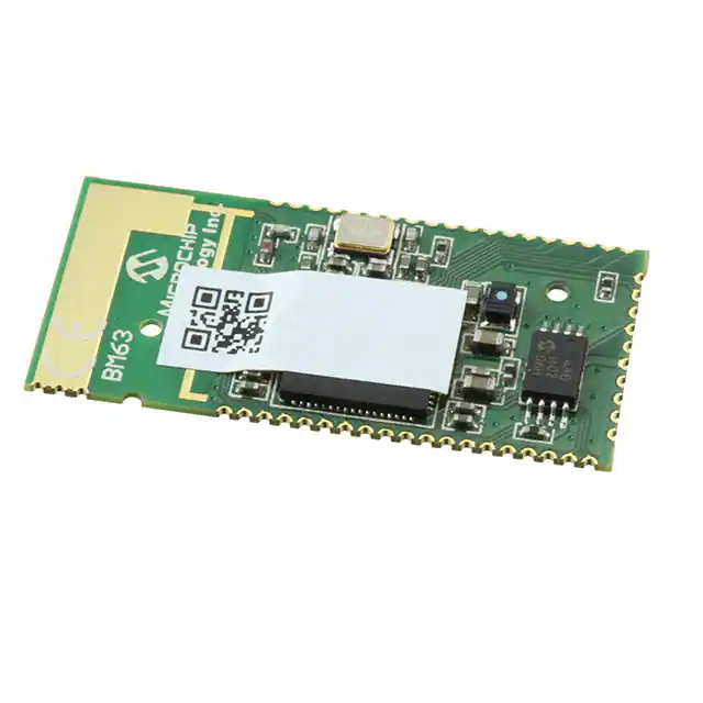
BM63
Bluetooth® 4.2 Stereo Audio Module
FIGURE 1:
Features
• Qualified for Bluetooth v4.2 specifications
• Supports HFP 1.6, HSP 1.2, A2DP 1.3, SPP 1.2
and AVRCP 1.6
• Supports Bluetooth 4.2 dual-mode (BDR/EDR/
BLE) specifications (FW dependent)
• Stand-alone module with on-board PCB antenna
and Bluetooth stack
• Supports high resolution up to 24-bit, 96 kHz
audio data format
• Supports to connect two hosts with HFP/A2DP
profiles simultaneously
• Supports to connect one host with SPP/BTLE
• Transparent UART mode for seamless serial data
over UART interface
• Easy to configure with Windows® GUI or directly
by external MCU
• Supports firmware field upgrade
• Supports one microphone
• Castellated surface mount pads for easy and reliable host PCB mounting
• RoHS compliant
• Ideal for portable battery operated devices
• Internal battery regulator circuitry
DSP Audio Processing
• Supports 64 kbps A-Law, -Law PCM format/
Continuous Variable Slope Delta (CVSD)
modulation for SCO channel operation
• Supports 8/16 kHz noise suppression
• Supports 8/16 kHz echo cancellation
• Supports Modified Sub-Band Coding (MSBC)
decoder for wide band speech
• Built-in High Definition Clean Audio (HCA) algorithms for both narrow band and wide band
speech processing
• Packet loss concealment (PLC)
• Built-in audio effect algorithms to enhance audio
streaming
• Supports Serial Copy Management System
(SCMS-T) content protection
2016-2017 Microchip Technology Inc.
BM63 MODULE
Audio Codec
• Sub-band Coding (SBC) and optional Advanced
Audio Coding (AAC) decoding
• 20-bit digital-to-analog converter (DAC) with
98 dB SNR
• 16-bit analog-to-digital converter (ADC) with
92 dB SNR
• Supports up to 24-bit, 96 kHz I2S digital audio
Peripherals
• Built-in lithium-ion and lithium-polymer battery
charger (up to 350 mA)
• Integrated 1.8V and 3V configurable switching
regulator and low-dropout (LDO) regulator
• Built-in ADC for battery voltage sense
• An AUX-In port for external audio input
• Three LED drivers
• Multiple I/O pins for control and status
Preliminary
DS60001431B-Page 1
�BM63
RF/Analog
Description
• Frequency spectrum: 2.402 GHz to 2.480 GHz
• Receive sensitivity: -90 dBm (2 Mbps EDR)
• Class 2 output power (+2 dBm typical)
The BM63 module is a fully qualified Bluetooth v4.2
dual-mode (BDR/EDR/BLE) module for designers to
add wireless audio and voice applications to their
products. The BM63 module is a Bluetooth Special
Interest Group (SIG) certified module that provides a
complete wireless solution with a Bluetooth stack and
an integrated PCB antenna in a compact surfacemount package.
HCI Interface
• High-speed HCI-UART interface (supports up to
921,600 bps)
MAC/Baseband Processor
• Supports Bluetooth 4.2 dual-mode (FW
dependent)
- BDR/EDR transport for audio, voice and SPP
data exchange
- BLE transport for proprietary transparent
service and Apple Notification Center Service
(ANCS) data exchange
The BM63 module has an integrated lithium-ion and
lithium-polymer battery charger, and a digital audio
interface. The module supports HSP, HFP, SPP, A2DP
and AVRCP profiles, and AAC and SBC codecs.
Operating Condition
• Operating voltage: 3.2V to 4.2V
• Operating temperature: -20°C to +70°C
Compliance
• Bluetooth SIG QDID: 83345
Applications
• Soundbar and Subwoofer (FW dependent)
• Bluetooth portable speaker phone
• Multi-speaker (FW dependent)
DS60001431B-Page 2
Preliminary
2016-2017 Microchip Technology Inc.
�BM63
Table of Contents
1.0 Device Overview ....................................................................................................................................................... 5
2.0 Audio ....................................................................................................................................................................... 13
3.0 Transceiver ............................................................................................................................................................. 17
4.0 Power Management Unit ........................................................................................................................................ 19
5.0 Application Information ........................................................................................................................................... 21
6.0 Printed Antenna Information ................................................................................................................................... 33
7.0 Physical Dimensions ............................................................................................................................................... 37
8.0 Electrical Characteristics......................................................................................................................................... 39
9.0 Soldering Recommendations .................................................................................................................................. 47
10.0 Ordering Information ............................................................................................................................................. 49
Appendix A: Revision History........................................................................................................................................ 51
TO OUR VALUED CUSTOMERS
It is our intention to provide our valued customers with the best documentation possible to ensure successful use of your Microchip
products. To this end, we will continue to improve our publications to better suit your needs. Our publications will be refined and
enhanced as new volumes and updates are introduced.
If you have any questions or comments regarding this publication, please contact the Marketing Communications Department via
E-mail at docerrorsmicrochip.com or fax the Reader Response Form in the back of this data sheet to (480) 792-4150. We welcome your feedback.
Most Current Data Sheet
To obtain the most up-to-date version of this data sheet, please register at our Worldwide Web site at:
http://www.microchip.com
You can determine the version of a data sheet by examining its literature number found on the bottom outside corner of any page.
The last character of the literature number is the version number, (e.g., DS30000000A is version A of document DS30000000).
Errata
An errata sheet, describing minor operational differences from the data sheet and recommended workarounds, may exist for current
devices. As device/documentation issues become known to us, we will publish an errata sheet. The errata will specify the revision
of silicon and revision of document to which it applies.
To determine if an errata sheet exists for a particular device, please check with one of the following:
• Microchip’s Worldwide Web site; http://www.microchip.com
• Your local Microchip sales office (see last page)
When contacting a sales office, please specify which device, revision of silicon and data sheet (include literature number) you are
using.
Customer Notification System
Register on our web site at www.microchip.com to receive the most current information on all of our products.
2016-2017 Microchip Technology Inc.
Preliminary
DS60001431B-Page 3
�BM63
NOTES:
DS60001431B-Page 4
Preliminary
2016-2017 Microchip Technology Inc.
�BM63
1.0
DEVICE OVERVIEW
The BM63 module is built around Microchip
Technology IS2063 SoC. The IS2063 SoC integrates
the Bluetooth 4.2 dual-mode radio transceiver, Power
Management Unit (PMU), crystal and DSP. Users can
configure the BM63 module by using the UI tool and
DSP tool, a Windows-based utility.
FIGURE 1-1:
Note:
The UI and DSP tools are available for
download from the Microchip web site at:
www.microchip.com/BM63.
Figure 1-1 illustrates a typical example of the
BM63 module which is connected to an external MCU
and a DSP/codec.
APPLICATION USING BM63 MODULE
2016-2017 Microchip Technology Inc.
Preliminary
DS60001431B-Page 5
�FIGURE 1-2:
SOUNDBAR AND SUBWOOFER APPLICATIONS USING BM63 MODULE
Preliminary
Figure 1-3 illustrates the Soundbar and Subwoofer applications using the BM63 module and smartphone.
FIGURE 1-3:
SOUNDBAR AND SUBWOOFER APPLICATIONS USING BM63 MODULE AND SMARTPHONE
BM63
DS60001431B-Page 6
Figure 1-2 illustrates the Soundbar and Subwoofer applications using the BM63 module.
2016-2017 Microchip Technology Inc.
� 2016-2017 Microchip Technology Inc.
Figure 1-4 illustrates the Multi-speaker application using the BM63 module.
FIGURE 1-4:
MULTI-SPEAKER APPLICATION USING BM63 MODULE
Preliminary
BM63
DS60001431B-Page 7
�BM63
Table 1-1 provides the key features of the BM63 module.
TABLE 1-1:
BM63 KEY FEATURES
Feature
BM63
Application
Multi-speaker/Soundbar/Subwoofer
Stereo/mono
Stereo
Pin count
48
Dimensions (mm2)
15 x 32
PCB antenna
Yes
Tx power (typical)
2 dBm
Audio DAC output
2 Channel
DAC (single-ended) SNR at 2.8V (dB)
-98
DAC (capless) SNR at 2.8V (dB)
-98
ADC SNR at 2.8V (dB)
-92
I
2S
digital interface
Yes
Analog AUX-In
Yes
Mono MIC
1
External audio amplifier interface
Yes
UART
Yes
USB
Yes
LED driver
3
Internal DC-DC step down regulator
Yes
DC 5V adapter input
Yes
Battery charger (350 mA max)
Yes
ADC for thermal charger protection
No
Undervoltage protection (UVP)
No
GPIO
15
Button support
6
NFC (triggered by external NFC)
Yes
EEPROM
Yes
Voice prompt (FW dependent)
8K Sampling Rate, stored in EEPROM with
approximately 800 bytes/second
Multi-tone
Yes
DSP sound effect
Yes
BLE
Yes
Bluetooth profiles
HFP
1.6
AVRCP
1.6
A2DP
1.3
HSP
1.2
SPP
1.2
DS60001431B-Page 8
Preliminary
2016-2017 Microchip Technology Inc.
�BM63
Figure 1-5 illustrates the pin diagram of the BM63
module.
FIGURE 1-5:
BM63 MODULE PIN DIAGRAM
2016-2017 Microchip Technology Inc.
Preliminary
DS60001431B-Page 9
�BM63
Table 1-2 provides the pin description of the BM63
module.
TABLE 1-2:
BM63 MODULE PIN DESCRIPTION
Pin No
Pin Type
Name
1
I
DR0
I2S interface: digital left/right data
Description
2
I/O
RFS0
I2S interface: left/right clock
3
I/O
SCLK0
4
O
DT0
5
O
AOHPR
6
O
AOHPM
Headphone common mode output/sense input
7
O
AOHPL
Left-channel, analog headphone output
8
I
MIC_N1
MIC1 mono differential analog negative input
9
I
MIC_P1
MIC1 mono differential analog positive input
10
P
MIC_BIAS
11
I
AIR
I2S interface: bit clock
I2S interface: digital left/right data
Right-channel, analog headphone output
Electric microphone biasing voltage
Right-channel, single-ended analog input
12
I
AIL
13
I/O
P1_2
EEPROM clock SCL
14
I/O
P1_3
EEPROM data SDA
15
I
RST_N
16
I/O
P0_1
Configurable control or indication pin
(Internally pulled-up if configured as an input)
• FWD key when Class 2 RF (default), active-low
• Class 1 Tx control signal for external RF Tx/Rx switch,
active-high
17
I/O
P2_4
System configuration pin along with P2_0 and EAN
pins used to set the module in any one of these modes:
• Application mode (for normal operation)
• Test mode (to change EEPROM values)
• Write Flash mode (to load a new firmware into the module), refer to Table 5-1
18
I/O
P0_4
Configurable control or indication pin
(Internally pulled-up if configured as an input)
• NFC detection pin, active-low
• Out_Ind_1
19
I/O
P1_5
Configurable control or indication pin
(Internally pulled-up if configured as an input)
• NFC detection pin, active-low
• Slide switch detector, active-high
• Out_Ind_1
• Multi-SPK Master/Slave mode control (FW dependent)
20
I
HCI_RXD
21
O
HCI_TXD
22
P
CODEC_VO
23
P
VDD_IO
I/O positive supply. Do not connect, for internal use only
24
P
ADAP_IN
5V power adapter input
DS60001431B-Page 10
Left-channel, single-ended analog input
System Reset (active-low)
HCI-UART data input
HCI-UART data output
Power supply/reference voltage for codec. Do not connect, for
internal use only
Preliminary
2016-2017 Microchip Technology Inc.
�BM63
TABLE 1-2:
BM63 MODULE PIN DESCRIPTION (CONTINUED)
Pin No
Pin Type
Name
25
P
BAT_IN
Battery input.
Voltage range: 3.2V to 4.2V. When an external power supply
is connected to the ADAP_IN pin, the BAT_IN pin can be left
open if battery is not connected.
26
P
ADC_IN
Analog input
27
P
SYS_PWR
28
I
MFB
• Multi-Function Button and power-on key
• UART RX_IND, active-high (used by host MCU to
wakeup the Bluetooth system)
29
I
LED3
LED driver 3
30
I
LED2
LED driver 2
31
I
LED1
LED driver 1
32
P
GND
Ground reference
33
I/O
P3_7
Configurable control or indication pin
(Internally pulled-up if configured as an input)
UART TX_IND, active-low (used by Bluetooth system to
wakeup the host MCU)
34
I/O
P3_5
Configurable control or indication pin
(Internally pulled-up, if configured as an input)
• Slide switch detector, active-high
35
I/O
P0_0
Configurable control or indication pin
(Internally pulled-up if configured as an input)
• Slide switch detector, active-high, Out_Ind_0
36
I/O
P0_3
Configurable control or indication pin
(Internally pulled-up if configured as an input)
• REV key (default), active-low
• Buzzer signal output
• Out_Ind_2
• Class 1 Rx Control signal of external RF Tx/Rx switch,
active-high
37
I
EAN
External address bus negative; must be pulled-down with
4.7 kOhm to GND
System configuration pin along with P2_0 and P2_4 pins,
used to set the module in any one of these modes:
• Application mode (for normal operation)
• Test mode (to change EEPROM values)
• Write Flash mode (to load a new firmware into the module), refer to Table 5-1
38
I/O
DM
Differential data-minus USB
39
I/O
DP
Differential data-plus USB
40
I/O
P3_6
Configurable control or indication pin
(Internally pulled-up if configured as an input)
Multi-SPK Master/Slave mode control (FW dependent)
41
I/O
P3_3
Configurable control or indication pin
(Internally pulled-up if configured as an input)
FWD key (default), active-low
42
I/O
P3_1
Configurable control or indication pin
(Internally pulled-up if configured as an input)
REV key (default), active-low
2016-2017 Microchip Technology Inc.
Description
System power output derived from ADAP_IN or BAT_IN
Preliminary
DS60001431B-Page 11
�BM63
TABLE 1-2:
BM63 MODULE PIN DESCRIPTION (CONTINUED)
Pin No
Pin Type
Name
43
I/O
P0_2
Configurable control or indication pin
(Internally pulled-up if configured as an input)
Play/Pause key (default)
44
I/O
P2_0
System configuration pin along with P2_4 and EAN pins used
to set the module in one of these modes:
• Application mode (for normal operation)
• Test mode (to change EEPROM values)
• Write Flash mode (to load a new firmware into the module), refer to Table 5-1
• Pulse/PWM signal output
45
I/O
P2_7
Configurable control or indication pin
(Internally pulled-up if configured as an input)
Volume-up key (default), active-low
46
I/O
P3_0
Configurable control or indication pin
(Internally pulled-up if configured as an input)
AUX-In detector, active-low
47
I/O
P0_5
Configurable control or indication pin
(Internally pulled-up if configured as an input)
Volume-down key (default), active-low
48
Legend:
Note:
P
I= Input pin
Description
GND
Ground reference
O= Output pin
I/O= Input/Output pin
P= Power pin
All I/O pins can be configured using the UI tool, a Windows utility.
DS60001431B-Page 12
Preliminary
2016-2017 Microchip Technology Inc.
�BM63
2.0
AUDIO
The input and output audios have different stages and
each stage can be programmed to vary the
characteristics of the gain response. For microphones,
both single-ended inputs and differential inputs are
supported. To maintain a high quality signal, a stable
bias voltage source to the condenser microphone’s
FET is provided. The DC blocking capacitors can be
used at both positive and negative sides of a input.
Internally, this analog signal is converted to 16-bit, 8/16
kHz linear PCM data.
2.1
Digital Signal Processor
A Digital Signal Processor (DSP) is used to perform
speech and audio processing. The advanced speech
features, such as acoustic echo cancellation and noise
reduction are inbuilt. To reduce nonlinear distortion and
to help echo cancellation, an outgoing signal level to
FIGURE 2-1:
SPEECH SIGNAL PROCESSING
FIGURE 2-2:
AUDIO SIGNAL PROCESSING
2016-2017 Microchip Technology Inc.
the speaker is monitored and adjusted to avoid saturation of speaker output or microphone input. Adaptive filtering is also applied to track the echo path impulse in
response to provide echo free and full-duplex user
experience.
The embedded noise reduction algorithm helps to
extract clean speech signals from the noisy input captured by the microphones, and improves mutual understanding in communication.
The advanced audio features, such as multi-band
dynamic range control, parametric multi-band
equalizer, audio widening and virtual bass are inbuilt.
The audio effect algorithms improve the user’s audio
listening experience in terms of better audio quality
after audio signal processing.
Figure 2-1 and Figure 2-2 illustrate the processing flow
of speaker-phone applications for speech and audio
signal processing.
Preliminary
DS60001431B-Page 13
�BM63
Users can configure DSP parameters using the DSP
tool. For additional information on the DSP tool, refer to
the “IS206X DSP Application Note”.
Note:
The DSP tool and “IS206X DSP Application Note” document, are available for
download from the Microchip web site at:
www.microchip.com/BM63.
FIGURE 2-3:
Note:
Codec
The built-in codec has a high signal-to-noise ratio
(SNR) performance and it consists of an ADC, a DAC
and an additional analog circuitry.
Figure 2-3 through Figure 2-6 illustrate the dynamic
range and frequency response of the codec.
CODEC DAC DYNAMIC RANGE
The data corresponds to the 16 Ohm load with 2.8V operating voltage at +25°C room temperature.
FIGURE 2-4:
Note:
2.2
CODEC DAC THD+N VERSUS INPUT POWER
The data corresponds to the 16 Ohm load with 2.8V operating voltage at +25°C room temperature.
DS60001431B-Page 14
Preliminary
2016-2017 Microchip Technology Inc.
�BM63
FIGURE 2-5:
CODEC DAC FREQUENCY RESPONSE (CAPLESS MODE)
FIGURE 2-6:
CODEC DAC FREQUENCY RESPONSE (SINGLE-ENDED MODE)
Note:
The DAC frequency response corresponds to single-ended mode with a 47 μF DC block capacitor.
2016-2017 Microchip Technology Inc.
Preliminary
DS60001431B-Page 15
�BM63
2.3
Auxiliary Port
2.4
The BM63 module supports analog (line-in) signals
from the external audio source. The analog (line-in) signal can be processed by the DSP to generate different
sound effects (Multi-band dynamic range compression
and audio widening), which can be configured by using
the DSP tool.
Analog Speaker Output
The BM63 module supports the following analog
speaker output modes:
• Capless mode – Recommended for headphone
applications in which capless output connection
helps to save the BOM cost by avoiding a large
DC blocking capacitor. Figure 2-7 illustrates the
analog speaker output capless mode
• Single-ended mode – Used for driving an external
audio amplifier where a DC blocking capacitor is
required. Figure 2-8 illustrates the analog speaker
output single-ended mode
FIGURE 2-7:
ANALOG SPEAKER OUTPUT CAPLESS MODE
FIGURE 2-8:
ANALOG SPEAKER OUTPUT SINGLE-ENDED MODE
DS60001431B-Page 16
Preliminary
2016-2017 Microchip Technology Inc.
�BM63
3.0
TRANSCEIVER
3.3
The BM63 module is designed and optimized for Bluetooth 2.4 GHz system. It contains a complete radio frequency transmitter/receiver section. An internal
synthesizer generates a stable clock for synchronizing
with another device.
3.1
Transmitter
The internal power amplifier (PA) has a maximum output power of +4 dBm. This is applied for Class 2 or
Class 3 radios without an external RF PA.
The transmitter performs the IQ conversion to minimize
the frequency drift.
3.2
Receiver
The low-noise amplifier (LNA) operates with TR-combined mode for single port application. It can save a pin
on the package without having an external Tx/Rx
switch.
The ADC can sample the input analog signal and convert it into a digital signal for demodulator analysis. A
channel filter has been integrated into receiver channel
before the ADC, which is used to reduce the external
component count and increase the anti-interference
capability.
The image rejection filter is used to reject the image
frequency for low-IF architecture. This filter for low-IF
architecture is intended to reduce external Band Pass
Filter (BPF) component for a super heterodyne
architecture.
Synthesizer
A synthesizer generates a clock for radio transceiver
operation. There is a VCO inside, with a tunable
internal LC tank that can reduce variation for
components. A crystal oscillator with an internal digital
trimming circuit provides a stable clock for the
synthesizer.
3.4
Modem
For Bluetooth 1.2 specification and below, 1 Mbps was
the standard data rate based on the Gaussian Frequency Shift Keying (GFSK) modulation scheme. This
basic rate modem meets Basic Data Rate (BDR)
requirements of Bluetooth 2.0 with Enhanced Data
Rate (EDR) specifications.
For Bluetooth 2.0 and above specifications, EDR has
been introduced to provide the data rates of
1/2/3 Mbps. For baseband, both BDR and EDR utilize
the same 1 MHz symbol rate and 1.6 kHz slot rate. For
BDR, symbol 1 represents 1-bit. However, each symbol in the payload part of EDR packets represents
2/3 bits. This is achieved by using two different modulations, π/4 DQPSK and 8 DPSK.
3.5
Adaptive Frequency Hopping
(AFH)
The BM63 module has an AFH function to avoid RF
interference. It has an algorithm to check the nearby
interference and to choose clear channel for transceiver Bluetooth signal.
The Received Signal Strength Indicator (RSSI) signal
feedback to the processor is used to control the RF
output power to make a good trade-off for effective
distance and current consumption.
2016-2017 Microchip Technology Inc.
Preliminary
DS60001431B-Page 17
�BM63
NOTES:
DS60001431B-Page 18
Preliminary
2016-2017 Microchip Technology Inc.
�BM63
4.0
POWER MANAGEMENT UNIT
The on-chip Power Management Unit (PMU) has two
main features: lithium-ion and lithium-polymer battery
charger, and voltage regulator. A power switch is used
to switch over the power source between the battery
and an adapter. Also, the PMU provides current to
drive three LEDs.
4.1
Charging a Battery
The BM63 module has a built-in battery charger which
is optimized for lithium-ion and lithium-polymer batteries.
The battery charger includes a current sensor for
charging control, user programmable current
regulation and high accuracy voltage regulation.
The charging current parameters are configured by the
UI tool. Reviving, pre-charging, constant current and
constant voltage modes and re-charging functions are
included. The maximum charging current is 350 mA.
Figure 4-1 illustrates the charging curve of a battery.
FIGURE 4-1:
4.2
BATTERY CHARGING CURVE
Voltage Monitoring
4.3
A 10-bit successive approximation register ADC (SAR
ADC) provides a dedicated channel for battery voltage
level detection. The warning level can be programmed
by using the UI tool. The ADC provides a granular resolution to enable the external MCU to take control over
the charging process.
2016-2017 Microchip Technology Inc.
LED Driver
Three dedicated LED drivers control the LEDs. They
provide enough sink current (16 step control and
0.35 mA for each step), thus LEDs can be connected
with the BM63 module. The LED settings can be configured using the UI tool.
Preliminary
DS60001431B-Page 19
�BM63
Figure 4-2 illustrates the LED drivers in the BM63
module.
FIGURE 4-2:
4.4
LED DRIVER
Under Voltage Protection
When the voltage of the SYS_PWR pin drops below the
voltage level of 2.9V, the system will shutdown automatically.
DS60001431B-Page 20
Preliminary
2016-2017 Microchip Technology Inc.
�BM63
5.0
APPLICATION INFORMATION
5.1
Host MCU Interface
The BM63 module supports UART commands. The
UART commands enable an external MCU to control
the BM63 module. Figure 5-1 illustrates the UART
interface between the BM63 module and an external
MCU.
FIGURE 5-1:
HOST MCU INTERFACE OVER UART
An external MCU can control the BM63 module over
the UART interface and wakeup the module with the
MFB and P3_7 pins.
Refer to the “UART_CommandSet” document for a list
of functions the BM63 module supports and how to use
the UI tool to configure the UART and UART Command
Set tool.
Note:
The UART Command set tool (SPKCommandSetTool v160.xx) and “UART_CommandSet” document are available for
download from the Microchip web site at:
www.microchip.com/BM63.
2016-2017 Microchip Technology Inc.
Preliminary
DS60001431B-Page 21
�FIGURE 5-2:
POWER-ON/OFF SEQUENCE
BM63
DS60001431B-Page 22
Figure 5-2 through Figure 5-6 illustrate the timing sequences of various UART
control signals.
Preliminary
2016-2017 Microchip Technology Inc.
�BM63
FIGURE 5-3:
TIMING SEQUENCE OF RX INDICATION AFTER POWER-ON STATE
FIGURE 5-4:
TIMING SEQUENCE OF POWER-OFF STATE
Note 1: EEPROM clock = 100 kHz.
2: For a byte write: 0.01 ms x 32 clock x 2 = 640 μs.
3: It is recommended to have a ramp-down time more than 640 μs during the power-off sequence to
ensure safe operation of the device.
2016-2017 Microchip Technology Inc.
Preliminary
DS60001431B-Page 23
�BM63
FIGURE 5-5:
TIMING SEQUENCE OF POWER-ON (NACK)
FIGURE 5-6:
RESET TIMING SEQUENCE IN CASE OF NO RESPONSE FROM MODULE TO
HOST MCU
Note:
When the host MCU sends a UART command and the BM63 module does not respond, the MCU
resends the UART command. If the BM63 module does not respond within 5 secs, the MCU will force
the system to Reset.
DS60001431B-Page 24
Preliminary
2016-2017 Microchip Technology Inc.
�BM63
5.2
I2S Mode Application
The BM63 module provides an I2S digital audio output
interface to connect with an external codec/DSP. It provides 8, 16, 44.1, 48, 88.2 and 96 kHz sampling rates
for 16-bit and 24-bit data formats. The I2S setting can
be configured using the UI and DSP tools.
Figure 5-7 and Figure 5-8 illustrate the I2S signal connection between the BM63 module and an external
DSP. Use the DSP tool to configure the BM63 module
as a Master/Slave.
For additional information on timing specifications,
refer to 8.2 “Timing specifications”.
FIGURE 5-7:
BM63 MODULE IN I2S MASTER MODE
FIGURE 5-8:
BM63 MODULE IN I2S SLAVE MODE
5.3
Reset
The BM63 module provides a watchdog timer (WDT) to
reset the chip. It has an integrated Power-on Reset
(POR) circuit that resets all circuits to a known
Power-on state. This action can be driven by an external Reset signal which is used to control the device
externally by forcing it into a POR state. The RST_N
signal input is active-low and no connection is required
in most of the applications.
2016-2017 Microchip Technology Inc.
Preliminary
DS60001431B-Page 25
�BM63
5.4
External Configuration and
Programming
The BM63 module can be configured by using an external configuration tool (EEPROM tool) and the firmware
is programmed by using a programming tool (Flash
tool).
Note:
The EEPROM and Flash tools are available for download from the Microchip web
site at: www.microchip.com/BM63.
Figure 5-9 illustrates the configuration and firmware
programming interface on the BM63 module. It is
recommended to include a header pin on the main PCB
for development.
FIGURE 5-9:
EXTERNAL PROGRAMMING HEADER CONNECTIONS
Configuration and firmware programming modes are
entered according to the system configuration I/O pins.
The P2_0, P2_4 and EAN pins have internal pull up.
TABLE 5-1:
Table 5-1 provides the system configuration settings.
SYSTEM CONFIGURATION I/O PINSETTINGS
Pins
Operating Mode
P2_0
P2_4
EAN
High
High
Low (Flash), High (ROM)
APP mode (Normal operation)
Low
High
Low (Flash), High (ROM)
Test mode (Write EEPROM)
Low
Low
High
Write Flash
DS60001431B-Page 26
Preliminary
2016-2017 Microchip Technology Inc.
� 2016-2017 Microchip Technology Inc.
5.5
Reference Circuit
Figure 5-10 through Figure 5-14 illustrate the BM63 module reference circuit for
a stereo headset applications.
FIGURE 5-10:
BM63 REFERENCE CIRCUIT FOR STEREO HEADSET APPLICATIONS
Preliminary
BM63
DS60001431B-Page 27
�BM63
BM63 REFERENCE CIRCUIT FOR STEREO HEADSET APPLICATIONS
DS60001431B-Page 28
FIGURE 5-11:
Preliminary
2016-2017 Microchip Technology Inc.
�BM63 REFERENCE CIRCUIT FOR STEREO HEADSET APPLICATIONS
2016-2017 Microchip Technology Inc.
FIGURE 5-12:
Preliminary
BM63
DS60001431B-Page 29
�BM63
BM63 REFERENCE CIRCUIT FOR STEREO HEADSET APPLICATIONS
DS60001431B-Page 30
FIGURE 5-13:
Preliminary
2016-2017 Microchip Technology Inc.
�BM63
FIGURE 5-14:
BM63 REFERENCE CIRCUIT FOR STEREO HEADSET APPLICATIONS
2016-2017 Microchip Technology Inc.
Preliminary
DS60001431B-Page 31
�BM63
NOTES:
DS60001431B-Page 32
Preliminary
2016-2017 Microchip Technology Inc.
�BM63
6.0
PRINTED ANTENNA
INFORMATION
6.1
Antenna Radiation Pattern
The BM63 module is integrated with one PCB printed
antenna, see Figure 6-1.
FIGURE 6-1:
RECOMMENDED KEEPOUT AREA FOR PCB ANTENNA
2016-2017 Microchip Technology Inc.
Preliminary
DS60001431B-Page 33
�BM63
Figure 6-2 illustrates the 3D radiation pattern of the
PCB printed antenna at 2441 MHz.
FIGURE 6-2:
PCB ANTENNA 3D RADIATION PATTERN AT 2441 MHZ
Table 6-1 provides the PCB Antenna characteristics of
BM63 module.
TABLE 6-1:
BM63 PCB ANTENNA
CHARACTERISTICS
Parameter
Values
Frequency
2400 MHz to 2480 MHz
Peak Gain
1.927 dBi
Efficiency
73.41%
6.2
Module Placement Guidelines
For Bluetooth-enabled products, the antenna placement
affects the overall performance of the system. The
antenna requires free space to radiate RF signals and it
must not be surrounded by the ground plane. Microchip
recommends that the area underneath the antenna on the
host PCB must not contain copper on the top, inner, or
bottom layers, as illustrated in Figure 6-1.
A low-impedance ground plane will ensure the best radio
performance (best range, lowest noise). The ground
plane can be extended beyond the minimum recommendation, as required for the main PCB EMC noise reduction. For the best range performance, keep all external
metal at least 15 mm away from the on-board PCB trace
antenna.
DS60001431B-Page 34
Preliminary
2016-2017 Microchip Technology Inc.
�BM63
Figure 6-3 and Figure 6-4 illustrate the examples of good
and poor placement of the BM63 module on a host board
with GND plane.
FIGURE 6-3:
BM63 MODULE PLACEMENT GUIDELINES
FIGURE 6-4:
GND PLANE ON MAIN APPLICATION BOARD
2016-2017 Microchip Technology Inc.
Preliminary
DS60001431B-Page 35
�BM63
NOTES:
DS60001431B-Page 36
Preliminary
2016-2017 Microchip Technology Inc.
�BM63
7.0
PHYSICAL DIMENSIONS
Figure 7-1 illustrates the PCB dimensions of the BM63
module.
FIGURE 7-1:
Note:
BM63 MODULE PCB DIMENSIONS
PCB dimensions: X: 15.0 mm, Y: 32.0 mm and tolerances: 0.25 mm
2016-2017 Microchip Technology Inc.
Preliminary
DS60001431B-Page 37
�BM63
Figure 7-2 illustrates the recommended PCB footprint
of the BM63 module
FIGURE 7-2:
RECOMMENDED BM63 MODULE PCB FOOTPRINT
Note 1: The keep-out area is reserved to keep the RF test point away from GND plane.
2: All metal keep-out is used to isolate the PCB antenna.
DS60001431B-Page 38
Preliminary
2016-2017 Microchip Technology Inc.
�BM63
8.0
ELECTRICAL CHARACTERISTICS
This section provides an overview of the BM63 module electrical characteristics. Additional information will be
provided in future revisions of this document as it becomes available.
Absolute maximum ratings for the BM63 module are listed below. Exposure to these maximum rating conditions for
extended periods may affect device reliability. Functional operation of the device at these or any other conditions, above
the parameters indicated in the operation listings of this specification, is not implied.
8.1
Absolute Maximum Ratings
Ambient temperature under bias.............................................................................................................. .-20°C to +70°C
Storage temperature ...............................................................................................................................-40°C to +125°C
Voltage on VDD with respect to VSS ......................................................................................................... -0.3V to +3.6V
Maximum output current sink by any I/O pin..........................................................................................................12 mA
Maximum output current sourced by any I/O pin....................................................................................................12 mA
Note:
Stresses listed under “Absolute Maximum Ratings” may cause permanent damage to the device. This
is a stress rating only. The functional operation of the device at those or any other conditions and those
indicated in the operation listings of this specification, is not implied. Exposure to maximum rating conditions for extended periods may affect device reliability.
2016-2017 Microchip Technology Inc.
Preliminary
DS60001431B-Page 39
�BM63
Table 8-1 through Table 8-10 provide the recommended operating conditions and the electrical specifications of the BM63 module.
TABLE 8-1:
RECOMMENDED OPERATING CONDITION
Symbol
Parameter
Min.
Typ.
Max.
Unit
BAT_IN
Input voltage for battery
3.2
3.8
4.2
V
ADAP_IN
Input voltage for adapter
4.5
5
5.5
V
Operation temperature
-20
+25
+70
ºC
TOPERATION
Note:
The absolute and recommended operating condition tables reflect a typical voltage usage for the device.
TABLE 8-2:
I/O AND RESET LEVEL
Parameter
Min.
Typ.
Max.
Unit
3.0
3.3
3.6
V
VIL input logic levels low
0
–
0.8
V
VIH input logic levels high
2.0
–
3.6
V
VOL output logic levels low
–
–
0.4
V
VOH output logic levels high
2.4
–
–
V
–
0.8
–
V
Min.
Typ.
Max.
Unit
4.5
5.0
5.5
V
I/O Supply Voltage (VDD_IO)
I/O Voltage Levels
RST_N
Threshold voltage
Note:
These parameters are characterized, but not tested in manufacturing.
TABLE 8-3:
BATTERY CHARGER
Parameter
ADAP_IN Input Voltage
Supply current to charger only
–
3
4.5
mA
Maximum Battery
Fast Charge Current
Headroom > 0.7V
(ADAP_IN = 5V)
–
350
–
mA
Headroom = 0.3V to 0.7V
(ADAP_IN = 4.5V)
–
175(2)
–
mA
Trickle Charge Voltage Threshold
–
3
–
V
Battery Charge Termination Current,
(% of Fast Charge Current)
–
10
–
%
Note 1: Headroom = VADAP_IN – VBAT
2: When VADAP_IN – VBAT > 2V, the maximum fast charge current is 175 mA for thermal protection.
3: These parameters are characterized, but not tested in manufacturing.
DS60001431B-Page 40
Preliminary
2016-2017 Microchip Technology Inc.
�BM63
TABLE 8-4:
LED DRIVER
Min.
Typ.
Max.
Unit
Open-drain Voltage
Parameter
–
–
3.6
V
Programmable Current Range
0
–
5.25
mA
Intensity Control
–
16
–
step
Current Step
–
0.35
–
mA
Power Down Open-drain Current
–
–
1
μA
Shutdown Current
–
–
1
μA
Min.
Typ.
Max.
Unit
Resolution
–
–
16
Bit
Output Sample Rate
8
–
48
kHz
Signal to Noise Ratio (Note 1)
(SNR at MIC or Line-in mode)
–
92
–
dB
Note 1: Test condition: BK_OUT = 1.8V with +25ºC temperature.
2: These parameters are characterized, but not tested in manufacturing.
TABLE 8-5:
T=
25oC,
AUDIO CODEC ANALOG TO DIGITAL CONVERTER
VDD = 2.8V, 1 kHz sine wave input, Bandwidth = 20 Hz to 20 kHz
Parameter (Condition)
Digital Gain
-54
–
4.85
dB
Digital Gain Resolution
–
2 to 6
–
dB
MIC Boost Gain
–
20
–
dB
Analog Gain
–
–
60
dB
Analog Gain Resolution
–
2.0
–
dB
Input full-scale at maximum gain (differential)
–
4
–
mV/rms
Input full-scale at minimum gain (differential)
–
800
–
mV/rms
3 dB bandwidth
–
20
–
kHz
Microphone mode (input impedance)
–
24
–
kOhm
THD+N (microphone input) at 30 mV/rms input
–
0.02
–
%
Note 1: fIN = 1 kHz, B/W = 20 Hz to 20 kHz, A-weighted, THD+N < 1%, 150 mVPP input.
2: These parameters are characterized, but not tested in manufacturing.
2016-2017 Microchip Technology Inc.
Preliminary
DS60001431B-Page 41
�BM63
TABLE 8-6:
AUDIO CODEC DIGITAL TO ANALOG CONVERTER
T = 25oC, VDD = 2.8V, 1 kHz sine wave input, Bandwidth = 20 Hz to 20 kHz
Parameter (Condition)
Min.
Typ.
Max.
Unit
Over-sampling rate
–
128
–
fs
Resolution
16
–
20
Bit
Output Sample Rate
8
–
48
kHz
Signal to Noise Ratio (Note 1)
(SNR at capless mode) for 48 kHz
–
98
–
dB
Signal to Noise Ratio (Note 1)
(SNR at single-ended mode) for 48 kHz
–
98
–
dB
-54
–
4.85
dB
–
2 to 6
–
dB
Digital Gain
Digital Gain Resolution
Analog Gain
-28
–
3
dB
–
1
–
dB
495
742.5
–
mV/rms
–
34.5
–
mW
Analog Gain Resolution
Output Voltage Full-scale Swing (AVDD = 2.8V)
Maximum Output Power (16 Ohm load)
Maximum Output Power (32 Ohm load)
–
17.2
–
mW
Resistive
–
16
O.C.
Ohm
Capacitive
–
–
500
pF
THD+N (16 Ohm load) (Note 2)
–
0.05
–
%
Signal to Noise Ratio (SNR at 16 Ohm load) (Note 3)
–
98
–
dB
Allowed Load
Note 1: fIN = 1 kHz, B/W = 20 Hz to 20 kHz, A-weighted, THD+N < 0.01%, 0 dBFS signal, Load = 100 kOhm
2: fIN = 1 kHz, B/W = 20 Hz to 20 kHz, A-weighted, -1 dBFS signal, Load = 16 Ohm
3: fIN = 1 kHz, B/W = 20 Hz to 20 kHz, A-weighted, THD+N < 0.05%, 0 dBFS signal, Load = 16 Ohm
4: These parameters are characterized but not tested in manufacturing.
TABLE 8-7:
TRANSMITTER SECTION FOR BDR AND EDR
Min.
Typ.
Max.
Bluetooth
specification
Unit
RF transmit power
–
2
–
-6 to 4
dBm
EDR/BDR Relative transmit power
-4
-1.8
1
-4 to 1
dB
Parameter
Note 1: The RF Tx power is modulation value.
2: The RF Transmit power is calibrated during the production by using the MP tool software and MT8852 Bluetooth Test equipment.
3: Test condition: VCC_RF = 1.28V, temperature +25ºC.
DS60001431B-Page 42
Preliminary
2016-2017 Microchip Technology Inc.
�BM63
TABLE 8-8:
RECEIVER SECTION FOR BDR AND EDR
Modulation
Min.
Typ.
Max.
Bluetooth
specification
Unit
Sensitivity at 0.1% BER
GFSK
–
-89
–
≤-70
dBm
Sensitivity at 0.01% BER
π/4 DQPSK
–
-90
–
≤-70
dBm
8 DPSK
–
-83
–
≤-70
dBm
Note 1: Test condition: VCC_RF = 1.28V with temperature +25ºC.
2: These parameters are characterized, but not tested in manufacturing.
TABLE 8-9:
BM63 SYSTEM CURRENT CONSUMPTION
Typ.(1)
Max.
Unit
–
10
μA
Standby mode
0.57
–
mA
Link mode
0.5
–
mA
ESCO link
15.1
–
mA
14.3
–
mA
Standby mode
0.6
–
mA
Link mode
0.6
–
mA
SCO link
15.3
–
mA
A2DP link
15.4
–
mA
System Status
System-Off mode
Stop advertising (Samsung S5 (SM-G900I)/Android™ 4.4.2)
A2DP link
Stop advertising
(iPhone®
6/iOS 8.4)
Note 1: The measurement data corresponds to Firmware v1.0.
2: Mode definition:
Standby mode: Power-on without Bluetooth link;
Link mode: With Bluetooth link in Low-power mode.
3: The current consumption values are measured with the BM63 EVB as a test platform, with BAT_IN = 3.8V.
The distance between the smartphone and BM63 EVB is 30 cm, and the speaker is without loading.
2016-2017 Microchip Technology Inc.
Preliminary
DS60001431B-Page 43
�BM63
8.2
Timing specifications
Figure 8-1 and Figure 8-2 illustrate the timing diagram
of the BM63 module in I2S and PCM modes.
FIGURE 8-1:
TIMING DIAGRAM FOR I2S MODES (MASTER/SLAVE)
FIGURE 8-2:
TIMING DIAGRAM FOR PCM MODES (MASTER/SLAVE)
Note 1: fs: 8,16, 32, 44.1, 48, 88.2 and 96 kHz.
2: SCLK0: 64*fs/256*fs.
3: Word length: 16-bit and 24-bit.
DS60001431B-Page 44
Preliminary
2016-2017 Microchip Technology Inc.
�BM63
Figure 8-3 illustrates the timing diagram of the audio
interface.
FIGURE 8-3:
AUDIO INTERFACE TIMING DIAGRAM
Table 8-10 provides the timing specifications of the
audio interface.
TABLE 8-10:
AUDIO INTERFACE TIMING SPECIFICATIONS
Parameter
Symbol
Min.
Typ.
Max.
Units
dSCLK
–
50
–
%
SCLK0 cycle time
tSCLKCY
50
–
–
ns
SCLK0 pulse width high
tSCLKCH
20
–
–
ns
SCLK0 pulse width low
tSCLKCL
20
–
–
ns
RFS0 Setup time to SCLK0 rising edge
tRFSSU
10
–
–
ns
RFS0 hold time from SCLK0 rising edge
tRFSH
10
–
–
ns
DR0 hold time from SCLK0 rising edge
tDH
10
–
–
ns
SCLK0 duty ratio
Note:
Test Conditions: Slave mode, fs = 48 kHz, 24-bit data and SCLK0 period = 256 fs.
2016-2017 Microchip Technology Inc.
Preliminary
DS60001431B-Page 45
�BM63
NOTES:
DS60001431B-Page 46
Preliminary
2016-2017 Microchip Technology Inc.
�BM63
9.0
SOLDERING RECOMMENDATIONS
The BM63 module is assembled using a standard
lead-free reflow profile, IPC/JEDEC J-STD-020. The
BM63 module can be soldered to the main PCB using a
standard leaded and lead-free solder reflow profiles.
To avoid the damage to the module, follow these recommendations:
• Refer to the “AN233 Solder Reflow Recommendation” (DS00233) document for the soldering reflow
recommendations
• The peak temperature (TP) must not exceed
+260ºC
• Refer to the “Solder Paste” data sheet for specific
reflow profile recommendations
FIGURE 9-1:
• Use no-clean flux solder paste
• Do not wash the module as moisture can be
trapped under the shield
• Use only one flow. If the PCB requires multiple
flows, apply the module on the final flow.
Figure 9-1 illustrates the reflow profile of the
BM63 module.
REFLOW PROFILE
2016-2017 Microchip Technology Inc.
Preliminary
DS60001431B-Page 47
�BM63
NOTES:
DS60001431B-Page 48
Preliminary
2016-2017 Microchip Technology Inc.
�BM63
10.0
ORDERING INFORMATION
Table 10-1 provides the ordering information of the
BM63 module.
TABLE 10-1:
Module
BM63
Note:
BM63 MODULE ORDERING INFORMATION
Microchip IC
IS2063GM
Description
Part No
2
Bluetooth 4.2 Stereo Audio with BLE, I S, Flash, Class 2,
no shield, built-in antenna
BM63SPKA1MC2
The BM63 module can be purchased through a Microchip representative.
Go to Microchip website www.microchip.com for the current pricing and a list of distributors for the product.
2016-2017 Microchip Technology Inc.
Preliminary
DS60001431B-Page 49
�BM63
NOTES:
DS60001431B-Page 50
Preliminary
2016-2017 Microchip Technology Inc.
�BM63
APPENDIX A:
REVISION HISTORY
Revision A (June 2016)
This is the initial released version of this document.
Revision B (January 2017)
This revision includes the following changes and minor
updates to text and formatting which were incorporated
throughout the document.
TABLE B-1:
MAJOR SECTION UPDATES
Section
Update Description
1.0 "Device Overview"
Added USB and updated the voice prompt details in Table 1-1.
Updated Table 1-2 with correct pin descriptions.
7.0 "Physical Dimensions"
Added Note to Figure 7-2.
2016-2017 Microchip Technology Inc.
Preliminary
DS60001431B-Page 51
�BM63
NOTES:
DS60001431B-Page 52
Preliminary
2016-2017 Microchip Technology Inc.
�BM63
THE MICROCHIP WEB SITE
CUSTOMER SUPPORT
Microchip provides online support via our WWW site at
www.microchip.com. This web site is used as a means
to make files and information easily available to
customers. Accessible by using your favorite Internet
browser, the web site contains the following
information:
Users of Microchip products can receive assistance
through several channels:
• Product Support – Data sheets and errata,
application notes and sample programs, design
resources, user’s guides and hardware support
documents, latest software releases and archived
software
• General Technical Support – Frequently Asked
Questions (FAQ), technical support requests,
online discussion groups, Microchip consultant
program member listing
• Business of Microchip – Product selector and
ordering guides, latest Microchip press releases,
listing of seminars and events, listings of
Microchip sales offices, distributors and factory
representatives
•
•
•
•
Distributor or Representative
Local Sales Office
Field Application Engineer (FAE)
Technical Support
Customers
should
contact
their
distributor,
representative or Field Application Engineer (FAE) for
support. Local sales offices are also available to help
customers. A listing of sales offices and locations is
included in the back of this document.
Technical support is available through the web site
at: http://microchip.com/support.
CUSTOMER CHANGE NOTIFICATION
SERVICE
Microchip’s customer notification service helps keep
customers current on Microchip products. Subscribers
will receive e-mail notification whenever there are
changes, updates, revisions or errata related to a
specified product family or development tool of interest.
To register, access the Microchip web site at
www.microchip.com. Under “Support”, click on
“Customer Change Notification” and follow the
registration instructions.
2016-2017 Microchip Technology Inc.
Preliminary
DS60001431B-Page 53
�BM63
NOTES:
DS60001431B-Page 54
Preliminary
2016-2017 Microchip Technology Inc.
�Note the following details of the code protection feature on Microchip devices:
•
Microchip products meet the specification contained in their particular Microchip Data Sheet.
•
Microchip believes that its family of products is one of the most secure families of its kind on the market today, when used in the
intended manner and under normal conditions.
•
There are dishonest and possibly illegal methods used to breach the code protection feature. All of these methods, to our
knowledge, require using the Microchip products in a manner outside the operating specifications contained in Microchip’s Data
Sheets. Most likely, the person doing so is engaged in theft of intellectual property.
•
Microchip is willing to work with the customer who is concerned about the integrity of their code.
•
Neither Microchip nor any other semiconductor manufacturer can guarantee the security of their code. Code protection does not
mean that we are guaranteeing the product as “unbreakable.”
Code protection is constantly evolving. We at Microchip are committed to continuously improving the code protection features of our
products. Attempts to break Microchip’s code protection feature may be a violation of the Digital Millennium Copyright Act. If such acts
allow unauthorized access to your software or other copyrighted work, you may have a right to sue for relief under that Act.
Information contained in this publication regarding device
applications and the like is provided only for your convenience
and may be superseded by updates. It is your responsibility to
ensure that your application meets with your specifications.
MICROCHIP MAKES NO REPRESENTATIONS OR
WARRANTIES OF ANY KIND WHETHER EXPRESS OR
IMPLIED, WRITTEN OR ORAL, STATUTORY OR
OTHERWISE, RELATED TO THE INFORMATION,
INCLUDING BUT NOT LIMITED TO ITS CONDITION,
QUALITY, PERFORMANCE, MERCHANTABILITY OR
FITNESS FOR PURPOSE. Microchip disclaims all liability
arising from this information and its use. Use of Microchip
devices in life support and/or safety applications is entirely at
the buyer’s risk, and the buyer agrees to defend, indemnify and
hold harmless Microchip from any and all damages, claims,
suits, or expenses resulting from such use. No licenses are
conveyed, implicitly or otherwise, under any Microchip
intellectual property rights unless otherwise stated.
Microchip received ISO/TS-16949:2009 certification for its worldwide
headquarters, design and wafer fabrication facilities in Chandler and
Tempe, Arizona; Gresham, Oregon and design centers in California
and India. The Company’s quality system processes and procedures
are for its PIC® MCUs and dsPIC® DSCs, KEELOQ® code hopping
devices, Serial EEPROMs, microperipherals, nonvolatile memory and
analog products. In addition, Microchip’s quality system for the design
and manufacture of development systems is ISO 9001:2000 certified.
QUALITY MANAGEMENT SYSTEM
CERTIFIED BY DNV
== ISO/TS 16949 ==
2016-2017 Microchip Technology Inc.
Trademarks
The Microchip name and logo, the Microchip logo, AnyRate, AVR,
AVR logo, AVR Freaks, BeaconThings, BitCloud, CryptoMemory,
CryptoRF, dsPIC, FlashFlex, flexPWR, Heldo, JukeBlox, KEELOQ,
KEELOQ logo, Kleer, LANCheck, LINK MD, maXStylus,
maXTouch, MediaLB, megaAVR, MOST, MOST logo, MPLAB,
OptoLyzer, PIC, picoPower, PICSTART, PIC32 logo, Prochip
Designer, QTouch, RightTouch, SAM-BA, SpyNIC, SST, SST
Logo, SuperFlash, tinyAVR, UNI/O, and XMEGA are registered
trademarks of Microchip Technology Incorporated in the U.S.A.
and other countries.
ClockWorks, The Embedded Control Solutions Company,
EtherSynch, Hyper Speed Control, HyperLight Load, IntelliMOS,
mTouch, Precision Edge, and Quiet-Wire are registered
trademarks of Microchip Technology Incorporated in the U.S.A.
Adjacent Key Suppression, AKS, Analog-for-the-Digital Age, Any
Capacitor, AnyIn, AnyOut, BodyCom, chipKIT, chipKIT logo,
CodeGuard, CryptoAuthentication, CryptoCompanion,
CryptoController, dsPICDEM, dsPICDEM.net, Dynamic Average
Matching, DAM, ECAN, EtherGREEN, In-Circuit Serial
Programming, ICSP, Inter-Chip Connectivity, JitterBlocker,
KleerNet, KleerNet logo, Mindi, MiWi, motorBench, MPASM, MPF,
MPLAB Certified logo, MPLIB, MPLINK, MultiTRAK, NetDetach,
Omniscient Code Generation, PICDEM, PICDEM.net, PICkit,
PICtail, PureSilicon, QMatrix, RightTouch logo, REAL ICE, Ripple
Blocker, SAM-ICE, Serial Quad I/O, SMART-I.S., SQI,
SuperSwitcher, SuperSwitcher II, Total Endurance, TSHARC,
USBCheck, VariSense, ViewSpan, WiperLock, Wireless DNA, and
ZENA are trademarks of Microchip Technology Incorporated in the
U.S.A. and other countries.
SQTP is a service mark of Microchip Technology Incorporated in
the U.S.A.
Silicon Storage Technology is a registered trademark of Microchip
Technology Inc. in other countries.
GestIC is a registered trademark of Microchip Technology
Germany II GmbH & Co. KG, a subsidiary of Microchip Technology
Inc., in other countries.
All other trademarks mentioned herein are property of their
respective companies.
© 2016-2017, Microchip Technology Incorporated, All Rights
Reserved.
ISBN: 978-1-5224-1256-4
Preliminary
DS60001431B-Page 55
�Worldwide Sales and Service
AMERICAS
ASIA/PACIFIC
ASIA/PACIFIC
EUROPE
Corporate Office
2355 West Chandler Blvd.
Chandler, AZ 85224-6199
Tel: 480-792-7200
Fax: 480-792-7277
Technical Support:
http://www.microchip.com/
support
Web Address:
www.microchip.com
Asia Pacific Office
Suites 3707-14, 37th Floor
Tower 6, The Gateway
Harbour City, Kowloon
China - Xiamen
Tel: 86-592-2388138
Fax: 86-592-2388130
Austria - Wels
Tel: 43-7242-2244-39
Fax: 43-7242-2244-393
China - Zhuhai
Tel: 86-756-3210040
Fax: 86-756-3210049
Denmark - Copenhagen
Tel: 45-4450-2828
Fax: 45-4485-2829
India - Bangalore
Tel: 91-80-3090-4444
Fax: 91-80-3090-4123
Finland - Espoo
Tel: 358-9-4520-820
Atlanta
Duluth, GA
Tel: 678-957-9614
Fax: 678-957-1455
Hong Kong
Tel: 852-2943-5100
Fax: 852-2401-3431
Australia - Sydney
Tel: 61-2-9868-6733
Fax: 61-2-9868-6755
China - Beijing
Tel: 86-10-8569-7000
Fax: 86-10-8528-2104
Austin, TX
Tel: 512-257-3370
China - Chengdu
Tel: 86-28-8665-5511
Fax: 86-28-8665-7889
Boston
Westborough, MA
Tel: 774-760-0087
Fax: 774-760-0088
China - Chongqing
Tel: 86-23-8980-9588
Fax: 86-23-8980-9500
Chicago
Itasca, IL
Tel: 630-285-0071
Fax: 630-285-0075
Dallas
Addison, TX
Tel: 972-818-7423
Fax: 972-818-2924
Detroit
Novi, MI
Tel: 248-848-4000
Houston, TX
Tel: 281-894-5983
Indianapolis
Noblesville, IN
Tel: 317-773-8323
Fax: 317-773-5453
Tel: 317-536-2380
Los Angeles
Mission Viejo, CA
Tel: 949-462-9523
Fax: 949-462-9608
Tel: 951-273-7800
Raleigh, NC
Tel: 919-844-7510
New York, NY
Tel: 631-435-6000
San Jose, CA
Tel: 408-735-9110
Tel: 408-436-4270
Canada - Toronto
Tel: 905-695-1980
Fax: 905-695-2078
DS60001431B-Page 56
France - Paris
Tel: 33-1-69-53-63-20
Fax: 33-1-69-30-90-79
India - New Delhi
Tel: 91-11-4160-8631
Fax: 91-11-4160-8632
France - Saint Cloud
Tel: 33-1-30-60-70-00
India - Pune
Tel: 91-20-3019-1500
Germany - Garching
Tel: 49-8931-9700
Germany - Haan
Tel: 49-2129-3766400
Japan - Osaka
Tel: 81-6-6152-7160
Fax: 81-6-6152-9310
China - Dongguan
Tel: 86-769-8702-9880
China - Guangzhou
Tel: 86-20-8755-8029
China - Hangzhou
Tel: 86-571-8792-8115
Fax: 86-571-8792-8116
China - Hong Kong SAR
Tel: 852-2943-5100
Fax: 852-2401-3431
China - Nanjing
Tel: 86-25-8473-2460
Fax: 86-25-8473-2470
China - Qingdao
Tel: 86-532-8502-7355
Fax: 86-532-8502-7205
China - Shanghai
Tel: 86-21-3326-8000
Fax: 86-21-3326-8021
China - Shenzhen
Tel: 86-755-8864-2200
Fax: 86-755-8203-1760
Germany - Karlsruhe
Tel: 49-721-625370
Korea - Daegu
Tel: 82-53-744-4301
Fax: 82-53-744-4302
Germany - Munich
Tel: 49-89-627-144-0
Fax: 49-89-627-144-44
Korea - Seoul
Tel: 82-2-554-7200
Fax: 82-2-558-5932 or
82-2-558-5934
Germany - Rosenheim
Tel: 49-8031-354-560
Malaysia - Kuala Lumpur
Tel: 60-3-6201-9857
Fax: 60-3-6201-9859
Malaysia - Penang
Tel: 60-4-227-8870
Fax: 60-4-227-4068
Philippines - Manila
Tel: 63-2-634-9065
Fax: 63-2-634-9069
Singapore
Tel: 65-6334-8870
Fax: 65-6334-8850
China - Shenyang
Tel: 86-24-2334-2829
Fax: 86-24-2334-2393
Germany - Heilbronn
Tel: 49-7131-67-3636
Japan - Tokyo
Tel: 81-3-6880- 3770
Fax: 81-3-6880-3771
Taiwan - Hsin Chu
Tel: 886-3-5778-366
Fax: 886-3-5770-955
Taiwan - Kaohsiung
Tel: 886-7-213-7830
China - Wuhan
Tel: 86-27-5980-5300
Fax: 86-27-5980-5118
Taiwan - Taipei
Tel: 886-2-2508-8600
Fax: 886-2-2508-0102
China - Xian
Tel: 86-29-8833-7252
Fax: 86-29-8833-7256
Thailand - Bangkok
Tel: 66-2-694-1351
Fax: 66-2-694-1350
Israel - Ra’anana
Tel: 972-9-744-7705
Italy - Milan
Tel: 39-0331-742611
Fax: 39-0331-466781
Italy - Padova
Tel: 39-049-7625286
Netherlands - Drunen
Tel: 31-416-690399
Fax: 31-416-690340
Norway - Trondheim
Tel: 47-7289-7561
Poland - Warsaw
Tel: 48-22-3325737
Romania - Bucharest
Tel: 40-21-407-87-50
Spain - Madrid
Tel: 34-91-708-08-90
Fax: 34-91-708-08-91
Sweden - Gothenberg
Tel: 46-31-704-60-40
Sweden - Stockholm
Tel: 46-8-5090-4654
UK - Wokingham
Tel: 44-118-921-5800
Fax: 44-118-921-5820
Preliminary
2016-2017 Microchip Technology Inc.
11/07/16
�