Supertex inc.
CL520
Linear, Fixed Constant Current
LED Driver
General Description
Features
The CL520 is a fixed, linear current regulator designed for
driving LEDs at 20mA. With a maximum rating of 90V, it is able
to withstand transients without the need for additional transient
protection circuitry. It is ideally suited for applications employing
single or multiple LEDs.
►► 20mA ±10% constant current drive
►► 1.0V dropout
►► 90V rating for transient immunity
►► Temperature compensated
►► 4.75 - 90V supply range
The minimum dropout voltage of 1.0V accomodates extra
LEDs, permits lower supply voltages, and provides more
efficient operation.
Applications
►► Specialty lighting
►► Low voltage signage
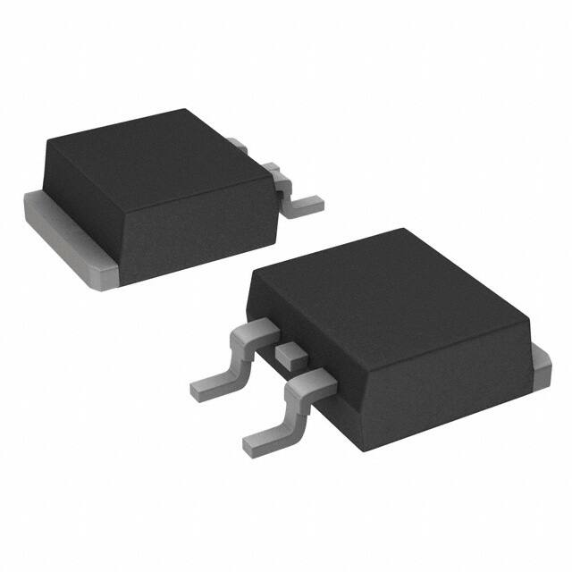
The CL520 is offered in TO-252(D-PAK) and TO-92 packages.
Typical Application Circuit
VIN
4.75 – 90V
100nF
20mA
OUT
VDD
Control
CL520
Doc.# DSFP-CL520
A052013
20mA
GND
Supertex inc.
www.supertex.com
�CL520
Pin Configurations
Ordering Information
Part Number
Package Options
Packing
CL520K4-G
TO-252 (D-PAK)
2000/Reel
CL520N3-G
TO-92
1000/Bag
CL520N3-G P002
TO-92
2000/Reel
CL520N3-G P003
TO-92
2000/Reel
CL520N3-G P005
TO-92
2000/Reel
CL520N3-G P013
TO-92
2000/Reel
CL520N3-G P014
TO-92
2000/Reel
GND
OUT
VDD
Package may or may not include the following marks: Si or
Value
Output voltage, VOUT
-0.5V to +100V
Operating junction temperature
-40°C to +125°C
Storage temperature
-65°C to +150°C
YY = Year Sealed
WW = Week Sealed
L = Lot Number
= “Green” Packaging
Si YYWW
CL520K4
LLLLLLL
Absolute Maximum Ratings
-0.5V to +100V
TO-92
Product Marking
Refer to ‘P0xx’ Tape & Reel Specs for P002, P003, P005, P013, and P014
TO-92 Taping Specifications and Winding Styles
Supply voltage, VDD
OUT
TO-252 (D-PAK)
-G denotes a lead (Pb)-free / RoHS compliant package
Parameter
GND
VDD
TO-252 (D-PAK)
Si C L
5 2 0
YYWW
Absolute Maximum Ratings are those values beyond which damage to the
device may occur. Functional operation under these conditions is not implied.
Continuous operation of the device at the absolute rating level may affect
device reliability. All voltages are referenced to device ground..
YY = Year Sealed
WW = Week Sealed
= “Green” Packaging
Package may or may not include the following marks: Si or
TO-92
Typical Thermal Resistance
Package
θja
TO-252 (D-PAK)
81OC/W*
TO-92
132OC/W*
* Mounted on JEDEC test PCB (2s 2p)
Recommended Operating Conditions (all voltages with respect to GND pin)
Sym
Parameter
Min
Typ
Max
Units
VDD
Supply voltage
4.75
-
90
V
---
VOUT
Voltage at OUT pin1
1.0
-
90
V
---
TJ
Junction temperature
-40
-
125
C
---
CDD
VDD bypass capacitor
100
-
-
Doc.# DSFP-CL520
A052013
2
o
Conditions
nF
Supertex inc.
www.supertex.com
�CL520
Electrical Characteristics
(Over recommended operating conditions. TA = 25OC unless otherwise specified. All voltages with respect to GND pin)
Sym
Parameter
IDD
Current into VDD pin
IOUT
Current into OUT pin
Min
Typ
Max
-
-
1.0
18
20
22
-
-
22
Units Conditions
mA
mA
--1.0V < VOUT < 90V
VOUT
很抱歉,暂时无法提供与“CL520K4-G”相匹配的价格&库存,您可以联系我们找货
免费人工找货- 国内价格
- 1+7.43040
- 10+7.23600
- 30+7.11720
- 国内价格 香港价格
- 2000+6.211482000+0.80401
- 国内价格 香港价格
- 1+8.098851+1.04831
- 25+6.8417825+0.88560
- 100+6.74882100+0.87357