Digital Power
Development Board
User’s Guide
2018 Microchip Technology Inc.
DS50002814A
�Note the following details of the code protection feature on Microchip devices:
•
Microchip products meet the specification contained in their particular Microchip Data Sheet.
•
Microchip believes that its family of products is one of the most secure families of its kind on the market today, when used in the
intended manner and under normal conditions.
•
There are dishonest and possibly illegal methods used to breach the code protection feature. All of these methods, to our
knowledge, require using the Microchip products in a manner outside the operating specifications contained in Microchip’s Data
Sheets. Most likely, the person doing so is engaged in theft of intellectual property.
•
Microchip is willing to work with the customer who is concerned about the integrity of their code.
•
Neither Microchip nor any other semiconductor manufacturer can guarantee the security of their code. Code protection does not
mean that we are guaranteeing the product as “unbreakable.”
Code protection is constantly evolving. We at Microchip are committed to continuously improving the code protection features of our
products. Attempts to break Microchip’s code protection feature may be a violation of the Digital Millennium Copyright Act. If such acts
allow unauthorized access to your software or other copyrighted work, you may have a right to sue for relief under that Act.
Information contained in this publication regarding device
applications and the like is provided only for your convenience
and may be superseded by updates. It is your responsibility to
ensure that your application meets with your specifications.
MICROCHIP MAKES NO REPRESENTATIONS OR
WARRANTIES OF ANY KIND WHETHER EXPRESS OR
IMPLIED, WRITTEN OR ORAL, STATUTORY OR
OTHERWISE, RELATED TO THE INFORMATION,
INCLUDING BUT NOT LIMITED TO ITS CONDITION,
QUALITY, PERFORMANCE, MERCHANTABILITY OR
FITNESS FOR PURPOSE. Microchip disclaims all liability
arising from this information and its use. Use of Microchip
devices in life support and/or safety applications is entirely at
the buyer’s risk, and the buyer agrees to defend, indemnify and
hold harmless Microchip from any and all damages, claims,
suits, or expenses resulting from such use. No licenses are
conveyed, implicitly or otherwise, under any Microchip
intellectual property rights unless otherwise stated.
Microchip received ISO/TS-16949:2009 certification for its worldwide
headquarters, design and wafer fabrication facilities in Chandler and
Tempe, Arizona; Gresham, Oregon and design centers in California
and India. The Company’s quality system processes and procedures
are for its PIC® MCUs and dsPIC® DSCs, KEELOQ® code hopping
devices, Serial EEPROMs, microperipherals, nonvolatile memory and
analog products. In addition, Microchip’s quality system for the design
and manufacture of development systems is ISO 9001:2000 certified.
QUALITY MANAGEMENT SYSTEM
CERTIFIED BY DNV
== ISO/TS 16949 ==
DS50002814A-page 2
Trademarks
The Microchip name and logo, the Microchip logo, AnyRate, AVR,
AVR logo, AVR Freaks, BitCloud, chipKIT, chipKIT logo,
CryptoMemory, CryptoRF, dsPIC, FlashFlex, flexPWR, Heldo,
JukeBlox, KeeLoq, Kleer, LANCheck, LINK MD, maXStylus,
maXTouch, MediaLB, megaAVR, MOST, MOST logo, MPLAB,
OptoLyzer, PIC, picoPower, PICSTART, PIC32 logo, Prochip
Designer, QTouch, SAM-BA, SpyNIC, SST, SST Logo,
SuperFlash, tinyAVR, UNI/O, and XMEGA are registered
trademarks of Microchip Technology Incorporated in the U.S.A.
and other countries.
ClockWorks, The Embedded Control Solutions Company,
EtherSynch, Hyper Speed Control, HyperLight Load, IntelliMOS,
mTouch, Precision Edge, and Quiet-Wire are registered
trademarks of Microchip Technology Incorporated in the U.S.A.
Adjacent Key Suppression, AKS, Analog-for-the-Digital Age, Any
Capacitor, AnyIn, AnyOut, BodyCom, CodeGuard,
CryptoAuthentication, CryptoAutomotive, CryptoCompanion,
CryptoController, dsPICDEM, dsPICDEM.net, Dynamic Average
Matching, DAM, ECAN, EtherGREEN, In-Circuit Serial
Programming, ICSP, INICnet, Inter-Chip Connectivity,
JitterBlocker, KleerNet, KleerNet logo, memBrain, Mindi, MiWi,
motorBench, MPASM, MPF, MPLAB Certified logo, MPLIB,
MPLINK, MultiTRAK, NetDetach, Omniscient Code Generation,
PICDEM, PICDEM.net, PICkit, PICtail, PowerSmart, PureSilicon,
QMatrix, REAL ICE, Ripple Blocker, SAM-ICE, Serial Quad I/O,
SMART-I.S., SQI, SuperSwitcher, SuperSwitcher II, Total
Endurance, TSHARC, USBCheck, VariSense, ViewSpan,
WiperLock, Wireless DNA, and ZENA are trademarks of
Microchip Technology Incorporated in the U.S.A. and other
countries.
SQTP is a service mark of Microchip Technology Incorporated in
the U.S.A.
Silicon Storage Technology is a registered trademark of
Microchip Technology Inc. in other countries.
GestIC is a registered trademark of Microchip Technology
Germany II GmbH & Co. KG, a subsidiary of Microchip
Technology Inc., in other countries.
All other trademarks mentioned herein are property of their
respective companies.
© 2018, Microchip Technology Incorporated, All Rights
Reserved.
ISBN: 978-1-5224-3762-8
2018 Microchip Technology Inc.
�DIGITAL POWER DEVELOPMENT
BOARD USER’S GUIDE
Table of Contents
Preface ........................................................................................................................... 5
Chapter 1. Overview....................................................................................................... 9
1.1 Introduction ..................................................................................................... 9
1.2 Features ......................................................................................................... 9
1.2.1 Socket for DP PIM Boards ........................................................................ 10
1.2.2 Test Points ................................................................................................ 10
1.2.3 Grounding System ..................................................................................... 11
1.2.4 External Analog Signal Input ..................................................................... 11
1.2.5 DC Level Insertion ..................................................................................... 11
1.2.6 Analog Input Connection Jumpers ............................................................ 11
1.2.7 Push Buttons ............................................................................................. 11
1.2.8 MikroBUS™ Socket ................................................................................... 11
1.2.9 ICSP™ Programming Port ........................................................................ 12
1.2.10 General Purpose Soldering Pad Area ..................................................... 12
1.2.11 Solder Pad for Ground Connection ......................................................... 12
1.2.12 USB Connector ....................................................................................... 12
1.2.13 On-Board LDO ........................................................................................ 12
1.2.14 Power Indicator LED ............................................................................... 12
1.2.15 User LEDs ............................................................................................... 12
1.3 Electrical Characteristics .............................................................................. 12
Appendix A. Board Layout and Schematics.............................................................. 13
A.1 Pinout ........................................................................................................... 13
A.2 Board Schematic .......................................................................................... 14
A.3 PCB Layout .................................................................................................. 15
Appendix B. Bill of Materials (BOM)........................................................................... 19
B.1 Bill of Materials ............................................................................................. 19
Worldwide Sales and Service .................................................................................... 22
2018 Microchip Technology Inc.
DS50002814A-page 3
�Digital Power Development Board User’s Guide
NOTES:
DS50002814A-page 4
2018 Microchip Technology Inc.
�DIGITAL POWER DEVELOPMENT
BOARD USER’S GUIDE
Preface
NOTICE TO CUSTOMERS
All documentation becomes dated, and this manual is no exception. Microchip tools and
documentation are constantly evolving to meet customer needs, so some actual dialogs
and/or tool descriptions may differ from those in this document. Please refer to our website
(www.microchip.com) to obtain the latest documentation available.
Documents are identified with a “DS” number. This number is located on the bottom of each
page, in front of the page number. The numbering convention for the DS number is
“DSXXXXXXXXA”, where “XXXXXXXX” is the document number and “A” is the revision level
of the document.
For the most up-to-date information on development tools, see the MPLAB® IDE online help.
Select the Help menu, and then Topics to open a list of available online help files.
INTRODUCTION
This chapter contains general information that will be useful to know before using the
Digital Power Development Board. Items discussed in this chapter include:
•
•
•
•
•
•
•
Document Layout
Conventions Used in this Guide
Recommended Reading
The Microchip Website
Product Change Notification Service
Customer Support
Document Revision History
DOCUMENT LAYOUT
This document describes how to use the Digital Power Development Board User’s
Guide as a demonstration tool to provide a measurement platform for the Microchip
dsPIC33 devices’ Digital Power Plug-In Modules. The document is organized as
follows:
• Chapter 1. “Overview” — This chapter introduces the Digital Power Development
Board and provides a brief overview of its various features.
• Appendix A. “Board Layout and Schematics” — This appendix presents the schematics and the board layouts for the Digital Power Development Board.
• Appendix B. “Bill of Materials (BOM)” — This appendix presents the Bill of Materials for the Digital Power Development Board.
2018 Microchip Technology Inc.
DS50002814A-page 5
�Digital Power Development Board User’s Guide
CONVENTIONS USED IN THIS GUIDE
This manual uses the following documentation conventions:
DOCUMENTATION CONVENTIONS
Description
Arial font:
Italic characters
Initial caps
Quotes
Underlined, italic text with
right angle bracket
Bold characters
N‘Rnnnn
Text in angle brackets < >
Courier New font:
Plain Courier New
Represents
Referenced books
Emphasized text
A window
A dialog
A menu selection
A field name in a window or
dialog
A menu path
MPLAB® IDE User’s Guide
...is the only compiler...
the Output window
the Settings dialog
select Enable Programmer
“Save project before build”
A dialog button
A tab
A number in verilog format,
where N is the total number of
digits, R is the radix and n is a
digit.
A key on the keyboard
Click OK
Click the Power tab
4‘b0010, 2‘hF1
Italic Courier New
Sample source code
Filenames
File paths
Keywords
Command-line options
Bit values
Constants
A variable argument
Square brackets [ ]
Optional arguments
Curly brackets and pipe
character: { | }
Ellipses...
Choice of mutually exclusive
arguments; an OR selection
Replaces repeated text
Represents code supplied by
user
DS50002814A-page 6
Examples
File>Save
Press ,
#define START
autoexec.bat
c:\mcc18\h
_asm, _endasm, static
-Opa+, -Opa0, 1
0xFF, ‘A’
file.o, where file can be
any valid filename
mcc18 [options] file
[options]
errorlevel {0|1}
var_name [,
var_name...]
void main (void)
{ ...
}
2018 Microchip Technology Inc.
�Preface
RECOMMENDED READING
This user’s guide describes how to use the Digital Power Development Board. Other
useful document(s) are listed below. The following Microchip document(s) are
recommended as supplemental reference resources.
• dsPIC33 Family Digital Power PIM User’s Guides are available for download
from the Microchip website (www.microchip.com)
THE MICROCHIP WEBSITE
Microchip provides online support via our website at www.microchip.com. This website
is used as a means to make files and information easily available to customers.
Accessible by using your favorite Internet browser, the website contains the following
information:
• Product Support – Data sheets and errata, application notes and sample
programs, design resources, user’s guides and hardware support documents,
latest software releases and archived software
• General Technical Support – Frequently Asked Questions (FAQs), technical
support requests, online discussion groups, Microchip consultant program
member listing
• Business of Microchip – Product selector and ordering guides, latest Microchip
press releases, listing of seminars and events; and listings of Microchip sales
offices, distributors and factory representatives
PRODUCT CHANGE NOTIFICATION SERVICE
Microchip’s customer notification service helps keep customers current on Microchip
products. Subscribers will receive e-mail notification whenever there are changes,
updates, revisions or errata related to a specified product family or development tool of
interest.
To register, access the Microchip website at www.microchip.com, click on Product
Change Notification and follow the registration instructions.
CUSTOMER SUPPORT
Users of Microchip products can receive assistance through several channels:
•
•
•
•
Distributor or Representative
Local Sales Office
Corporate Application Engineer (CAE)
Embedded Solutions Engineer (ESE)
Customers should contact their distributor, representative or Embedded Solutions
Engineer (ESE) for support. Local sales offices are also available to help customers.
A listing of sales offices and locations is included in the back of this document.
Technical support is available through the website at:
http://www.microchip.com/support.
DOCUMENT REVISION HISTORY
Revision A (October 2018)
This is the initial version of this document.
2018 Microchip Technology Inc.
DS50002814A-page 7
�Digital Power Development Board User’s Guide
NOTES:
DS50002814A-page 8
2018 Microchip Technology Inc.
�DIGITAL POWER DEVELOPMENT
BOARD USER’S GUIDE
Chapter 1. Overview
1.1
INTRODUCTION
The Digital Power Development Board is a demonstration board that provides the user
with a flexible measurement platform for all compatible Microchip dsPIC33 Digital
Power Plug-In Modules (DP PIMs). DP PIMs can be inserted into the mating socket J1
in the middle of the Digital Power Development Board. All pins of the DP PIM are
accessible via test loops or pin headers. The on-board micro USB connector provides
a DC power input to all circuitry. In addition, a mikroBUS™ socket is provided to extend
functionality.
This chapter provides an overview of the features of the Digital Power Development
Board. The topics covered include:
• Features
• Electrical Characteristics
1.2
FEATURES
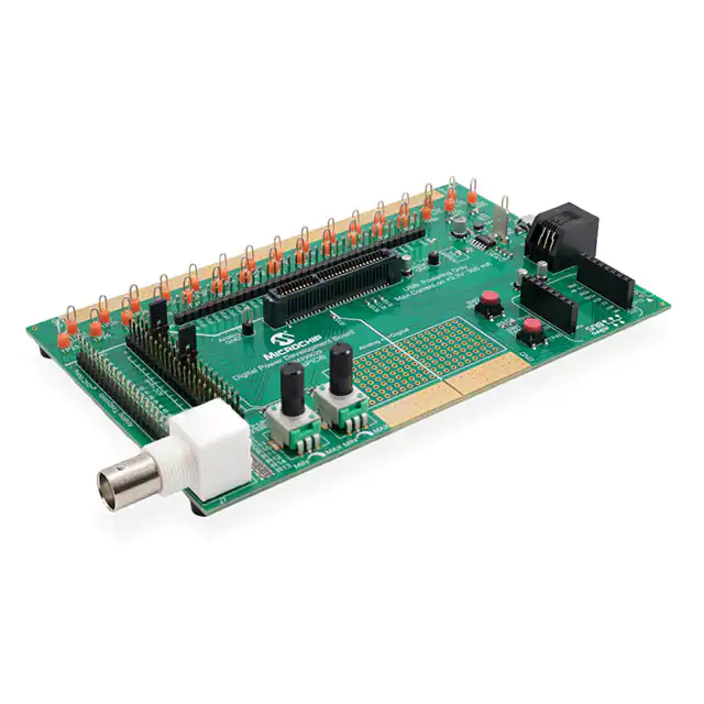
The Digital Power Development Board has the following features, as shown in Figure 1-1.
FIGURE 1-1:
DIGITAL POWER DEVELOPMENT BOARD
14
2
18
16
1
15
17
7
3
12
9
13
5
10
6
11
8
4
14
1.
2.
3.
4.
5.
Socket for DP PIM boards.
Digital GPIO test points. Pin header with connection to the digital test points.
ADC and DAC test points.
External analog signal input.
Potentiometer for DC level insertion from GND to +3.3V; it can be connected to
the lower half of the ADC inputs.
2018 Microchip Technology Inc.
DS50002814A-page 9
�Digital Power Development Board User’s Guide
6. Potentiometer for DC level insertion from GND to +3.3V; it can be connected to
the upper half of the ADC inputs.
7. Analog input connection jumpers.
8. User push button.
9. Reset push button.
10. mikroBUS socket.
11. ICSP™ header to program the on-board MCU (6-pin, 2.54 mm header).
12. ICSP header to program the on-board MCU (RJ25 connector).
13. General purpose soldering pad area.
14. Solder pads for ground connection.
15. USB connector.
16. On-board LDO with Power Good (PG) function.
17. Power indicator LED (Green).
18. User LEDs (Red and Green).
Board dimensions are: 160 mm (length) x 100 mm (height).
1.2.1
Socket for DP PIM Boards
Insert the DP PIM board under test into the socket located in the middle of the Digital
Power Development Board. Socket J1 has a slot that defines the DP PIM board
direction. Be careful not to break the slot when inserting the DP PIM board into
the socket.
1.2.2
Test Points
The Digital Power Development Board ensures good signal integrity and provides
access to all pins of a DP PIM board. Each signal line is named after the DP PIM edge
connector pin number, with a “TP” (Test Point) prefix on the schematic diagram, which
is similarly marked on the silkscreen. These signals are divided into two main sections:
Analog and Digital (see Figure 1-1). For a detailed pinout, refer to the User’s Guide of
the DP PIM under test.
1. Analog Section
The analog section is located at the left connector side (smaller sector of the
socket). It consists of 18 signal lines, all referenced to analog ground. These lines
are split into two subsections:
• ADC inputs
• DAC output
2. Digital Section
The digital section is located at the right connector side (larger sector of the
socket). It consists of 31 lines, all referenced to digital ground. These lines
support all the digital lines of the DP PIMs. Some of them have dedicated
functions, such as:
• High-speed PWM outputs
• Medium speed GPIO
• Communication lines (SPI, I2C, UART)
• User push button and LEDs
DS50002814A-page 10
2018 Microchip Technology Inc.
�Overview
1.2.3
Grounding System
The entire board ground potential is connected together and forms one galvanically
common domain. The labels, “Analog” and “Digital”, indicate the geometrical domain.
The copper pour connected to the ground potential is split into two geometrical
domains, but the two geometrical domains are jointed together under the PIM socket,
thus improving the signal integrity and keeping noise confined to near their sources.
1.2.4
External Analog Signal Input
It is possible to insert an analog signal to any ADC input from a signal generator via a
standard BNC connector. The input impedance is 50. Input signals between the
ground and +3.3V are accepted. An overvoltage protection is implemented on this input
with a series resistor, and a pair of parallel diodes between the ground and the positive
supply rail.
1.2.5
DC Level Insertion
Two on-board potentiometers are connected between the ground and the +3.3V supply
rail to provide two stable DC levels. The two DC levels can be set independently with
potentiometers: P1 and P2. These DC signals can be used as an input signal to any
ADC input. The DC level set by P1 can be connected to the upper half, while P2 can
be connected to the lower half of the ADC inputs, at the analog input connection
jumpers.
1.2.6
Analog Input Connection Jumpers
The ADC inputs of the DP PIM board can be accessed directly from the pin header (J3)
located at the left side of the board. These inputs can also be connected to either the
external analog signal input (J7) or to the DC level insertion, respectively. The
three-row pin header matrix, J4, J5, J6 (No. 7 in Figure 1-1), forms a three-pin selection
jumper for each ADC input. When placing a jumper over the left, or over the right and
the middle pins, the corresponding ADC input can be connected to the extra input as
indicated on the silkscreen. The left side pins connect the external analog signal input,
while the right side pins connect the DC level insertion to the given ADC input. Two
positions on the DAC outputs are not connected. The pins on those positions are just
placeholders to keep the pin order. Three pins are connected to GND at both ends of
the jumper row. Jumpers can be stored on those pins if not needed. Two jumpers are
provided in the kit.
1.2.7
Push Buttons
There are two push buttons on the board: SW1 and SW2. Push button SW2, which is
directly connected to the RESET pin of the DP PIM board, is for the system Reset. For
dual core devices, this RESET is connected to the Master core Reset line. Push button
SW1 is a general purpose user interface connected to the TP27 test point and the
corresponding pin on the DP PIM.
1.2.8
MikroBUS™ Socket
A standard extension socket (J10) is provided on the board for mikroBUS
click boards™. The functionality of the board can be easily extended by using this
feature. The DP PIM board communicates with the mikroBUS socket via dedicated SPI
lines and the I2C bus. Both +5V and +3.3V supply rails are connected to the
corresponding pins of the mikroBUS socket. The Reset button is connected to the
mikroBUS socket RESET pin.
2018 Microchip Technology Inc.
DS50002814A-page 11
�Digital Power Development Board User’s Guide
1.2.9
ICSP™ Programming Port
Dedicated lines for programming the MCU device on the inserted DP PIM board are
accessible via an RJ-25 modular connector or on a 6-pin header.
1.2.10
General Purpose Soldering Pad Area
The soldering point matrix on the bottom of the board with Plated-Through-Hole (PTH)
pads can be used to assemble any small extension circuitry needed for testing or
prototyping.
1.2.11
Solder Pad for Ground Connection
A bare gold-plated copper area is located on the upper and the bottom edges of the
board. These areas can either be used for soldering a solid ground connection or for
attaching alligator clips to connect instrument ground.
1.2.12
USB Connector
The Digital Power Development Board can be powered via the micro USB connector,
J2, at the right side of the board. The DP PIM board supply input and the +5V power
rail for the mikroBUS click board are directly connected to the positive supply line of the
USB. This connector is only for powering. The input voltage must be in the range of
3.6V to 6.3V. The mikroBUS click board can tighten this constraint; please refer to the
specifications before powering. Communication is not possible via this USB connector.
1.2.13
On-Board LDO
The +3.3V power rail for the mikroBUS click board is supplied by the on-board LDO
(Microchip’s MCP1755), connected to the +5V supply rail coming from the USB. The
total load for the mikroBUS click board supply current and the additional load caused
by its active GPIO lines should not exceed 300 mA. The DC level insertion
potentiometer and the pull-up resistor of the user push button are also connected to this
line. The Power Good output drives the Reset line of the board, ensuring stable
performance.
1.2.14
Power Indicator LED
The green LED (LD1) is on when the supply voltage is applied on the +5V supply rail.
1.2.15
User LEDs
The Digital Power Development Board has two user-programmable on-board LEDs.
The red LED is connected to TP52, while the green LED is connected to TP54. Logic
level high drives the LEDs.
1.3
ELECTRICAL CHARACTERISTICS
Table 1-1 shows the electrical characteristics of the Digital Power Development Board.
TABLE 1-1:
ELECTRICAL CHARACTERISTICS
Parameter
Input Voltage Range
DS50002814A-page 12
Value
3.6 VDC to 6.3 VDC
Current Consumption