ABRIDGED DATA SHEET
19-5256; Rev 1; 11/10
DS31400
8-Input, 14-Output, Dual DPLL Timing IC
with Sub-ps Output Jitter
General Description
The DS31400 is a flexible, high-performance timing IC
for diverse frequency conversion and frequency
synthesis applications. On each of its eight input clocks
and 14 output clocks, the device can accept or generate
nearly any frequency between 2kHz and 750MHz. The
device offers two independent DPLLs to serve two
independent clock-generation paths.
The input clocks are divided down, fractionally scaled as
needed, and continuously monitored for activity and
frequency accuracy. The best input clock is selected,
manually or automatically, as the reference clock for
each of the two flexible, high-performance digital PLLs.
Each DPLL lock to the selected reference and provides
programmable bandwidth, very high-resolution holdover
capability and truly hitless switching between input
clocks. The digital PLLs are followed by a clock
synthesis subsystem that has seven fully programmable
digital frequency synthesis blocks, three high-speed
low-jitter APLLs, and 14 output clocks, each with its own
32-bit divider and phase adjustment. The APLLs provide
fractional scaling and output jitter less than 1ps RMS.
For telecom systems, the device has all required
features and functions to serve as a central timing
function or as a line card timing IC. With a suitable
oscillator the device meets the requirements of Stratum
2, 3E, 3, 4E and 4; G.812 Types I–IV; G.813; and
G.8262.
Features
Eight Input Clocks
Differential or CMOS/TTL Format
Any Frequency from 2kHz to 750MHz
Fractional Scaling for 64B/66B and FEC Scaling (e.g.,
64/66, 237/255, 238/255) or Any Other
Downscaling Requirement
Continuous Input Clock Quality Monitoring
Automatic or Manual Clock Selection
Three 2/4/8kHz Frame Sync Inputs
Two High-Performance DPLLs
Hitless Reference Switching on Loss of Input
Automatic or Manual Phase Build-Out
Holdover on Loss of All Inputs
Programmable Bandwidth, 0.5mHz to 400Hz
Seven Digital Frequency Synthesizers
Each Can Slave to Either DPLL
Produce Any 2kHz Multiple Up to 77.76MHz
Per-DFS Clock Phase Adjust
Three Output APLLs
Output Frequencies to 750MHz
High Resolution Fractional Scaling for FEC and
64B/66B (e.g., 255/237, 255/238, 66/64) or Any
Other Scaling Requirement
Less than 1ps RMS Output Jitter
Simultaneously Produce Three Low-Jitter Rates from
the Same Reference (e.g., 622.08MHz for SONET,
255/237 x 622.08MHz for OTU2, and 156.25MHz
for 10GE)
14 Output Clocks in Seven Groups
Nearly Any Frequency from < 1Hz to 750MHz
Each Group Slaves to a DFS Clock, Any APLL Clock,
or Any Input Clock (Divided and Scaled)
Each Has a Differential Output (Three CML, Four LVDS/
LVPECL) and Separate CMOS/TTL Output
32-Bit Frequency Divider per Output
Two Sync Pulse Outputs: 8kHz and 2kHz
General Features
Suitable Line Card IC or Timing Card IC for Stratum
2/3E/3/4E/4, SMC, SEC/EEC, or SSU
Accepts and Produces Nearly Any Frequency Up to
750MHz, Including 1Hz, 2kHz, 8kHz, NxDS1,
NxE1, DS2/J2, DS3, E3, 2.5MHz, 25MHz, 125MHz,
156.25MHz, and Nx19.44MHz Up to 622.08MHz
Internal Compensation for Local Oscillator Frequency
Error
SPI™ Processor Interface
1.8V Operation with 3.3V I/O (5V Tolerant)
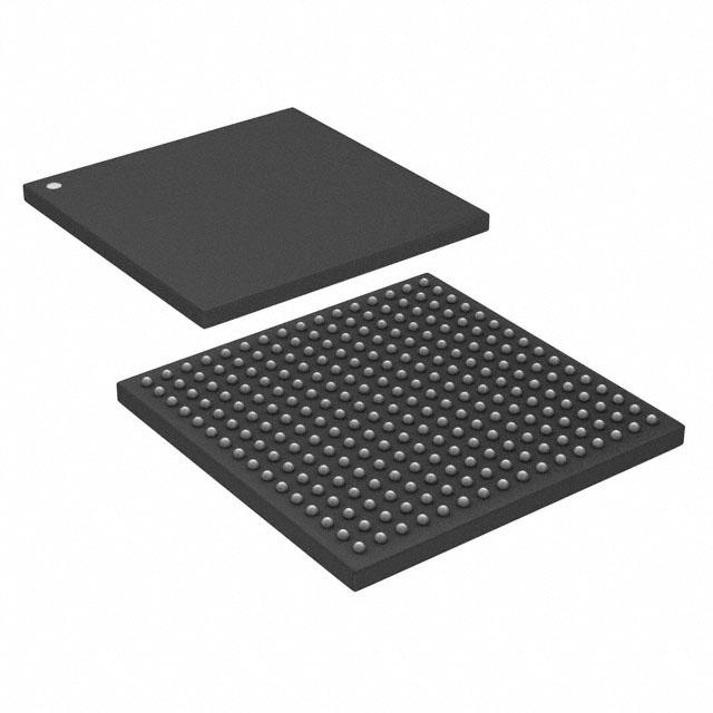
17mm x 17mm CSBGA Package
Applications
Frequency Conversion Applications in a Wide Variety of
Equipment Types
Telecom Line Cards or Timing Cards with Any Mix of
SONET/SDH, Synchronous Ethernet, and/or
OTN Ports in WAN Equipment Including MSPPs,
Ethernet Switches, Routers, DSLAMs, and Base
Stations
Ordering Information
PART
TEMP RANGE
PIN-PACKAGE
DS31400GN
DS31400GN+
-40C to +85C
-40C to +85C
256 CSBGA
256 CSBGA
+Denotes a lead(Pb)-free/RoHS-compliant package.
SPI is a trademark of Motorola, Inc.
Maxim Integrated Products 1
Some revisions of this device may incorporate deviations from published specifications known as errata. Multiple
revisions of any device may be simultaneously available through various sales channels. For information about device
errata, go to: www.maxim-ic.com/errata. For pricing, delivery, and ordering information, please contact Maxim Direct at
1-888-629-4642, or visit Maxim’s website at www.maxim-ic.com.
�ABRIDGED DATA SHEET
DS31400
Application Example: Timing Card
activity and frequency
monitoring, select highest priority
valid input for each DPLL
create derived DS1 or E1/2048kHz
clock locked to selected clock
Timing Card (1 of 2)
Backplane
DS1, E1 or
2048 kHz
DS31400
BITS
Tx
DPLL1
APLL and
divider
DPLL2
APLL,
divider and
fanout
Monitor,
Divider,
Selector
TCXO or
OCXO
from BITS/SSU
BITS
Rx
N
clock/data recovery,
equalizer, framer,
extract SSMs
to BITS/SSU
processor
N
typically 19.44MHz,
25MHz or 8kHz,
point-to-point
or multidrop buses
N
Stratum 2, 3E or 3:
jitter/wander filtering,
hitless switching,
phase adjust,
holdover
Timing Card (2 of 2)
Identical to Timing Card 1
N
Line Card
Timing IC
(see Fig 2-2)
Line Card (1 of N)
from port SERDES
to port SERDES
selects best system
clock, best recovered line
clock. hitless switching,
frequency conversion,
jitter cleanup
Line Card (N of N)
Application Example: Line Card
clock monitoring and selection,
hitless switching, holdover, frequency
conversion, fractional scaling,
jitter attenuation
19.44MHz, 38.88MHz,
25MHz, etc.
DS31400
system timing
from master and slave
timing cards
line timing
to master and slave
timing cards
IC1
IC2
DPLL1 Path
n
DPLL2 Path
n
OC1 to OC5
SONET/SDH, 1GE, 10GE, OTN, FC, etc.
3 unrelated frequencies simultaneously at